US10147757B2 - Image sensor structures for fingerprint sensing - Google Patents
Image sensor structures for fingerprint sensingDownload PDFInfo
- Publication number
- US10147757B2 US10147757B2US15/087,481US201615087481AUS10147757B2US 10147757 B2US10147757 B2US 10147757B2US 201615087481 AUS201615087481 AUS 201615087481AUS 10147757 B2US10147757 B2US 10147757B2
- Authority
- US
- United States
- Prior art keywords
- wafer
- image sensor
- light
- collimator filter
- collimator
- Prior art date
- Legal status (The legal status is an assumption and is not a legal conclusion. Google has not performed a legal analysis and makes no representation as to the accuracy of the status listed.)
- Active, expires
Links
Images


Classifications
- H01L27/14685—
- H—ELECTRICITY
- H10—SEMICONDUCTOR DEVICES; ELECTRIC SOLID-STATE DEVICES NOT OTHERWISE PROVIDED FOR
- H10F—INORGANIC SEMICONDUCTOR DEVICES SENSITIVE TO INFRARED RADIATION, LIGHT, ELECTROMAGNETIC RADIATION OF SHORTER WAVELENGTH OR CORPUSCULAR RADIATION
- H10F39/00—Integrated devices, or assemblies of multiple devices, comprising at least one element covered by group H10F30/00, e.g. radiation detectors comprising photodiode arrays
- H10F39/011—Manufacture or treatment of image sensors covered by group H10F39/12
- H10F39/024—Manufacture or treatment of image sensors covered by group H10F39/12 of coatings or optical elements
- G—PHYSICS
- G02—OPTICS
- G02B—OPTICAL ELEMENTS, SYSTEMS OR APPARATUS
- G02B27/00—Optical systems or apparatus not provided for by any of the groups G02B1/00 - G02B26/00, G02B30/00
- G02B27/30—Collimators
- G06K9/0004—
- G—PHYSICS
- G06—COMPUTING OR CALCULATING; COUNTING
- G06V—IMAGE OR VIDEO RECOGNITION OR UNDERSTANDING
- G06V40/00—Recognition of biometric, human-related or animal-related patterns in image or video data
- G06V40/10—Human or animal bodies, e.g. vehicle occupants or pedestrians; Body parts, e.g. hands
- G06V40/12—Fingerprints or palmprints
- G06V40/13—Sensors therefor
- G06V40/1318—Sensors therefor using electro-optical elements or layers, e.g. electroluminescent sensing
- H01L27/14625—
- H01L27/14632—
- H01L27/14687—
- H—ELECTRICITY
- H10—SEMICONDUCTOR DEVICES; ELECTRIC SOLID-STATE DEVICES NOT OTHERWISE PROVIDED FOR
- H10F—INORGANIC SEMICONDUCTOR DEVICES SENSITIVE TO INFRARED RADIATION, LIGHT, ELECTROMAGNETIC RADIATION OF SHORTER WAVELENGTH OR CORPUSCULAR RADIATION
- H10F39/00—Integrated devices, or assemblies of multiple devices, comprising at least one element covered by group H10F30/00, e.g. radiation detectors comprising photodiode arrays
- H10F39/011—Manufacture or treatment of image sensors covered by group H10F39/12
- H10F39/026—Wafer-level processing
- H—ELECTRICITY
- H10—SEMICONDUCTOR DEVICES; ELECTRIC SOLID-STATE DEVICES NOT OTHERWISE PROVIDED FOR
- H10F—INORGANIC SEMICONDUCTOR DEVICES SENSITIVE TO INFRARED RADIATION, LIGHT, ELECTROMAGNETIC RADIATION OF SHORTER WAVELENGTH OR CORPUSCULAR RADIATION
- H10F39/00—Integrated devices, or assemblies of multiple devices, comprising at least one element covered by group H10F30/00, e.g. radiation detectors comprising photodiode arrays
- H10F39/80—Constructional details of image sensors
- H10F39/806—Optical elements or arrangements associated with the image sensors
- G—PHYSICS
- G02—OPTICS
- G02B—OPTICAL ELEMENTS, SYSTEMS OR APPARATUS
- G02B5/00—Optical elements other than lenses
- G02B5/20—Filters
- G02B5/201—Filters in the form of arrays
- G—PHYSICS
- G02—OPTICS
- G02B—OPTICAL ELEMENTS, SYSTEMS OR APPARATUS
- G02B6/00—Light guides; Structural details of arrangements comprising light guides and other optical elements, e.g. couplings
- G02B6/04—Light guides; Structural details of arrangements comprising light guides and other optical elements, e.g. couplings formed by bundles of fibres
- G02B6/06—Light guides; Structural details of arrangements comprising light guides and other optical elements, e.g. couplings formed by bundles of fibres the relative position of the fibres being the same at both ends, e.g. for transporting images
- G02B6/08—Light guides; Structural details of arrangements comprising light guides and other optical elements, e.g. couplings formed by bundles of fibres the relative position of the fibres being the same at both ends, e.g. for transporting images with fibre bundle in form of plate
- H—ELECTRICITY
- H01—ELECTRIC ELEMENTS
- H01L—SEMICONDUCTOR DEVICES NOT COVERED BY CLASS H10
- H01L2224/00—Indexing scheme for arrangements for connecting or disconnecting semiconductor or solid-state bodies and methods related thereto as covered by H01L24/00
- H01L2224/01—Means for bonding being attached to, or being formed on, the surface to be connected, e.g. chip-to-package, die-attach, "first-level" interconnects; Manufacturing methods related thereto
- H01L2224/42—Wire connectors; Manufacturing methods related thereto
- H01L2224/47—Structure, shape, material or disposition of the wire connectors after the connecting process
- H01L2224/48—Structure, shape, material or disposition of the wire connectors after the connecting process of an individual wire connector
- H01L2224/4805—Shape
- H01L2224/4809—Loop shape
- H01L2224/48091—Arched
Definitions
- This disclosuregenerally relates to optical sensors, and more particularly to an optical sensor using a collimator.
- biometric recognition systemsimage biometric objects for authenticating and/or verifying users of devices incorporating the recognition systems.
- Biometric imagingprovides a reliable, non-intrusive way to verify individual identity for recognition purposes.
- Various types of sensorsmay be used for biometric imaging.
- Fingerprintslike various other biometric characteristics, are based on distinctive personal characteristics and thus provide a reliable mechanism to recognize an individual.
- fingerprint sensorshave many potential applications.
- fingerprint sensorsmay be used to provide access control in stationary applications, such as security checkpoints.
- Fingerprint sensorsmay also be used to provide access control in mobile devices, such as cell phones, wearable smart devices (e.g., smart watches and activity trackers), tablet computers, personal data assistants (PDAs), navigation devices, and portable gaming devices. Accordingly, some applications, in particular applications related to mobile devices, may require recognition systems that are both small in size and highly reliable.
- fingerprint sensors in most mobile devicesare capacitive sensors having a sensing array configured to sense ridge and valley features of a fingerprint.
- these fingerprint sensorseither detect absolute capacitance (sometimes known as “self-capacitance”) or trans-capacitance (sometimes known as “mutual capacitance”). In either case, capacitance at each sensing element in the array varies depending on whether a ridge or valley is present, and these variations are electrically detected to form an image of the fingerprint.
- capacitive fingerprint sensorsprovide certain advantages, most commercially available capacitive fingerprint sensors have difficulty sensing fine ridge and valley features through large distances, requiring the fingerprint to contact a sensing surface that is close to the sensing array. It remains a significant challenge for a capacitive sensor to detect fingerprints through thick layers, such as the thick cover glass (sometimes referred to herein as a “cover lens”) that protects the display of many smart phones and other mobile devices.
- a cutoutis often formed in the cover glass in an area beside the display, and a discrete capacitive fingerprint sensor (often integrated with a mechanical button) is placed in the cutout area so that it can detect fingerprints without having to sense through the cover glass.
- a discrete capacitive fingerprint sensoris placed in the cutout area so that it can detect fingerprints without having to sense through the cover glass.
- the need for a cutoutmakes it difficult to form a flush surface on the face of device, detracting from the user experience, and complicating the manufacture.
- the existence of mechanical buttonsalso takes up valuable
- Embodiments of the disclosureprovide methods and systems for integrating image sensor structures with collimator filters, including manufacturing methods and associated structures for forming collimator filters at the wafer level for integration with image sensor semiconductor wafers.
- a method of making an optical biometric sensortypically includes forming a collimator filter layer on an image sensor wafer, wherein a plurality of light collimating apertures in the collimator filter layer are aligned with a plurality of light sensing elements in the image sensor wafer, and after forming the collimator filter layer on the image sensor wafer, singulating the image sensor wafer into a plurality of individual optical sensors.
- forming the collimator filter layerincludes forming the plurality of light collimating apertures and routing circuitry for light sensing elements of the image sensor wafer in one or more redistribution layers disposed on a front side of the image sensor wafer.
- forming the plurality of collimator filter layercomprises forming the light collimating apertures into a back side of the image sensor wafer, wherein a front side of the image sensor wafer includes one or more redistribution layers.
- forming the collimator filter layer on the image sensor waferincludes forming a collimator filter wafer having the plurality of light collimating apertures, and attaching the collimator filter wafer to the image sensor wafer.
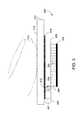
- FIG. 1is a block diagram of an example of a system that includes an optical sensor and a processing system, according to an embodiment of the disclosure.
- FIG. 2illustrates an example of a mobile device that includes an optical sensor according to an embodiment of the disclosure.
- FIG. 3illustrates an example of an optical sensor with a collimator filter layer according to an embodiment of the disclosure.
- FIG. 4illustrates an example of light interacting with an optical sensor having a collimator filter layer according to an embodiment of the disclosure.
- FIG. 5illustrates an alternative embodiment of a collimator filter layer according to an embodiment of the disclosure.
- FIG. 6illustrates a method of imaging an input object according to an embodiment of the disclosure.
- FIG. 7depicts an image sensor structure in accordance with the present disclosure.
- FIG. 8depicts another image sensor structure in accordance with the present disclosure. More specifically, FIG. 8 depicts a front-side illuminated CMOS detector, with a collimator filter etched into the RDL layer.
- FIG. 9depicts another image sensor structure in accordance with the present disclosure. More specifically, FIG. 9 depicts a front-side illuminated CMOS detector, with a collimator filter etched into the RDL layer, and with photo detectors that discriminate the angle of light.
- FIG. 10depicts another image sensor structure in accordance with the present disclosure. More specifically, FIG. 10 depicts a CMOS detector (sensor ASIC), with a collimator filter, and with a second ASIC (digital ASIC) mounted to it.
- CMOS detectorsensor ASIC
- collimator filtercollimator filter
- second ASICdigital ASIC
- FIG. 11depicts another image sensor structure in accordance with the present disclosure. More specifically, FIG. 11 depicts a Back-side illumination image sensor with TSV substrate mount
- FIG. 12depicts another image sensor structure in accordance with the present disclosure.
- FIG. 1Silicon collimator filter bonded to an image sensor
- FIG. 13depicts a process flow for forming an image sensor structure with a collimator filter in accordance with an embodiment of the present disclosure.
- FIG. 14depicts, on the LEFT: Wafer with etch mask attached to UV release tape, and on the RIGHT: Cross-section of unfinished collimator vias.
- FIG. 15depicts alignment of collimator filter to an image sensor.
- FIG. 16depicts wafer-to wafer bonding and removal of Si on top of bond pads (The dotted lines indicate scribe lines).
- FIG. 17depicts another process flow for an alternate way of forming an image sensor structure with a collimator filter in accordance with an embodiment of the present disclosure.
- FIG. 18depicts another process flow for an alternate way of forming an image sensor structure with a collimator filter in accordance with an embodiment of the present disclosure.
- an optical sensorincludes a collimator filter layer which operates as a light conditioning layer, interposed between a sensing region and an image sensor array.
- a collimator filter layerwhich operates as a light conditioning layer, interposed between a sensing region and an image sensor array.
- Light from a sensing regionis filtered by the collimator filter layer such that only certain of the reflected light beams reach optical sensing elements (also “sensing pixels” or “light sensing elements”) in the image sensor array.
- collimator filter layer of the present disclosureprevents blurring while allowing for a lower-profile image sensor, such as a fingerprint sensor, than is possible with purely lens-based or pinhole camera-based imaging sensors.
- the image sensorcan be made thin for use in mobile devices such as cell phones. Placing individual collimator apertures over each optical sensing element, or group of elements, provides better sensitivity than purely pinhole based imagers by transmitting more light to the optical sensing elements.
- the present disclosuredescribes the use of the collimator filter layer to enable optical sensing through a large range of thicknesses of cover layers.
- Embodiments of the disclosurealso provide methods and systems for integrating image sensor structures with collimator filters, including manufacturing methods and associated structures for forming collimator filters at the wafer level for integration with image sensor semiconductor wafers.
- FIG. 1is a block diagram of an example of an electronic system 100 that includes an optical sensor device 102 and a processing system 104 , according to an embodiment of the disclosure.
- the processing system 104includes processor(s) 106 , a memory 108 , a template storage 110 , an operating system (OS) 112 , and a power source 114 .
- processor(s) 106 , the memory 108 , the template storage 110 , and the operating system 112are interconnected physically, communicatively, and/or operatively for inter-component communications.
- the power source 114is interconnected to the various system components to provide electrical power as necessary.
- processor(s) 106are configured to implement functionality and/or process instructions for execution within electronic device 100 and the processing system 104 .
- processor(s) 106execute instructions stored in memory 108 or instructions stored on template storage 110 to identify a biometric object or determine whether a biometric authentication attempt is successful or unsuccessful.
- Memory 108which may be a non-transitory, computer-readable storage medium, is configured to store information within electronic device 100 during operation.
- memory 108includes a temporary memory, an area for information not to be maintained when the electronic device 100 is turned off. Examples of such temporary memory include volatile memories such as random access memories (RAM), dynamic random access memories (DRAM), and static random access memories (SRAM).
- RAMrandom access memories
- DRAMdynamic random access memories
- SRAMstatic random access memories
- Template storage 110comprises one or more non-transitory computer-readable storage media.
- the template storage 110is generally configured to store enrollment views for fingerprint images for a user's fingerprint or other enrollment information. More generally, the template storage 110 may be used to store information about an object. The template storage 110 may further be configured for long-term storage of information.
- the template storage 110includes non-volatile storage elements. Non-limiting examples of non-volatile storage elements include magnetic hard discs, solid-state drives (SSD), optical discs, floppy discs, flash memories, or forms of electrically programmable memories (EPROM) or electrically erasable and programmable (EEPROM) memories, among others.
- SSDsolid-state drives
- EPROMelectrically programmable memories
- EEPROMelectrically erasable and programmable
- the processing system 104also hosts an operating system (OS) 112 .
- the operating system 112controls operations of the components of the processing system 104 .
- the operating system 112facilitates the interaction of the processor(s) 106 , memory 108 and template storage 110 .
- the processor(s) 106implement hardware and/or software to obtain data describing an image of an input object.
- the processor(s) 106may also align two images and compare the aligned images to one another to determine whether there is a match.
- the processor(s) 106may also operate to reconstruct a larger image from a series of smaller partial images or sub-images, such as fingerprint images when multiple partial fingerprint images are collected during a biometric process, such as an enrollment or matching process for verification or identification.
- the processing system 104includes a power source 114 (or one or more power sources) to provide power to the electronic device 100 .
- a power source 114or one or more power sources
- the power source 114include single-use power sources, rechargeable power sources, and/or power sources developed from nickel-cadmium, lithium-ion, or other suitable material as well as power cords and/or adapters which are in turn connected to electrical power.
- Optical sensor 102can be implemented as a physical part of the electronic system 100 , or can be physically separate from the electronic system 100 . As appropriate, the optical sensor 102 may communicate with parts of the electronic system 100 using any one or more of the following: buses, networks, and other wired or wireless interconnections. In some embodiments, optical sensor 102 is implemented as a fingerprint sensor to capture a fingerprint image of a user. In accordance with the disclosure, the optical sensor 102 uses optical sensing for the purpose of object imaging including imaging biometrics such as fingerprints. The optical sensor 102 can be incorporated as part of a display, for example, or may be a discrete sensor.
- electronic systems 100include personal computers of all sizes and shapes, such as desktop computers, laptop computers, netbook computers, tablets, web browsers, e-book readers, and personal digital assistants (PDAs). Additional exemplary electronic systems 100 include composite input devices, such as physical keyboards and separate joysticks or key switches. Further exemplary electronic systems 100 include peripherals such as data input devices (including remote controls and mice) and data output devices (including display screens and printers). Other examples include remote terminals, kiosks, video game machines (e.g., video game consoles, portable gaming devices, and the like), communication devices (including cellular phones, such as smart phones), and media devices (including recorders, editors, and players such as televisions, set-top boxes, music players, digital photo frames, and digital cameras).
- PDAspersonal digital assistants
- Additional exemplary electronic systems 100include composite input devices, such as physical keyboards and separate joysticks or key switches. Further exemplary electronic systems 100 include peripherals such as data input devices (including remote controls and mice) and data output devices (including display screens and printers). Other examples include
- the optical sensor 102may provide illumination to the sensing region. Reflections from the sensing region in the illumination wavelength(s) are detected to determine input information corresponding to the input object.
- the optical sensor 102may utilize principles of direct illumination of the input object, which may or may not be in contact with a sensing surface of the sensing region depending on the configuration.
- One or more light sources and/or light guiding structuresmay be used to direct light to the sensing region. When an input object is present, this light is reflected from surfaces of the input object, which reflections can be detected by the optical sensing elements and used to determine information about the input object.
- the optical sensor 102may also utilize principles of internal reflection to detect input objects in contact with a sensing surface.
- One or more light sourcesmay be used to direct light in a light guiding element at an angle at which it is internally reflected at the sensing surface of the sensing region, due to different refractive indices at opposing sides of the boundary defined by the sensing surface.
- Contact of the sensing surface by the input objectcauses the refractive index to change across this boundary, which alters the internal reflection characteristics at the sensing surface, causing light reflected from the input object to be weaker at portions where it is in contact with the sensing surface.
- Higher contrast signalscan often be achieved if principles of frustrated total internal reflection (FTIR) are used to detect the input object.
- FTIRfrustrated total internal reflection
- the lightmay be directed to the sensing surface at an angle of incidence at which it is totally internally reflected, except where the input object is in contact with the sensing surface and causes the light to partially transmit across this interface.
- An example of thisis presence of a finger introduced to an input surface defined by a glass to air interface.
- the higher refractive index of human skin compared to aircauses light incident at the sensing surface at the critical angle of the interface to air to be partially transmitted through the finger, where it would otherwise be totally internally reflected at the glass to air interface.
- This optical responsecan be detected by the system and used to determine spatial information. In some embodiments, this can be used to image small scale fingerprint features, where the internal reflectivity of the incident light differs depending on whether a ridge or valley is in contact with that portion of the sensing surface.
- FIG. 2illustrates an example of an electronic device 116 , such as a mobile phone, which includes cover glass (or cover lens) 118 over a display 120 .
- the disclosed method and systemmay be implemented by using the display 120 as the optical sensor to image an input object.
- a separate discrete component 122provides the optical sensing capabilities.
- a separate discrete component 122 that provides optical sensing capabilitiescan be located under display 120 .
- FIG. 3illustrates an example of a stack-up for an optical image sensor device 200 used to image an object 216 , such as a fingerprint.
- the sensor 200includes an image sensor array 202 , a light collimator filter layer or light conditioning layer 204 disposed above the image sensor array 202 , an illumination layer 207 disposed above the collimator filter layer 204 , a light source 208 , and a cover layer 210 .
- a blocking layer 214may also be provided.
- the cover layer 210protects the inner components of the sensor 200 such as the image sensor array 202 .
- the cover layer 210may include a cover glass or cover lens that protects inner components of a display in addition to the sensor 200 .
- a sensing region for the input objectis defined above the cover layer 210 .
- a top surface 218 of the cover layer 210may form a sensing surface, which provides a contact area for the input object 216 (e.g., fingerprint).
- the cover layer 210is made of any material such as glass, transparent polymeric materials and the like.
- the input object 216is any object to be imaged.
- the object 216will have various features.
- the object 216has ridges and valleys. Due to their protruding nature, the ridges contact the sensing surface 218 of the cover 210 layer. In contrast, the valleys do not contact the sensing surface 218 and instead form an air gap between the input object 216 and the sensing surface 218 .
- the object 216may have other features such as stain, ink and the like that do not create significant structural differences in portions of the input object 216 , but which affect its optical properties.
- the methods and systems disclosed hereinare suitable for imaging such structural and non-structural features of the input object 216 .
- the illumination layer 207includes a light source 208 and/or a light guiding element 206 that directs illumination to the sensing region in order to image the input object.
- the light source 208transmits beams or rays of light 212 into the light guiding element 206 , and the transmitted light propagates through the light guiding element 206 .
- the light guiding elementmay utilize total internal reflection, or may include reflecting surfaces that extract light up towards the sensing region. Some of the light in the illumination layer may become incident at the sensing surface 218 in an area that is in contact with the input object 216 . The incident light is in turn reflected back towards the collimator filter layer 204 .
- the light source 208is disposed adjacent to the light guiding element 206 .
- the light source 208may be positioned anywhere within the sensor 200 provided that the emitted light reaches the light guiding element 206 .
- the light source 208may be disposed below the image sensor array 202 .
- a separate light guiding element 206is not required.
- the light transmitted from the light source 208can be transmitted directly into the cover layer 210 in which case the cover layer 210 also serves as the light guiding element.
- the light transmitted from the light source 208can be transmitted directly to the sensing region, in which case the light source 208 itself serves as the illumination layer.
- a discrete light sourceis also not required.
- the method and systemcontemplate using the light provided by a display or the backlighting from an LCD as suitable light sources.
- the light provided by the illumination layer 207 to image the object 216may be in near infrared (NIR) or visible.
- the lightcan have a narrow band of wavelengths, a broad band of wavelengths, or operate in several bands.
- the image sensor array 202detects light passing through the light collimator filter layer 204 .
- suitable sensor arraysare complementary metal oxide semiconductor (CMOS) and charge coupled device (CCD) sensor arrays.
- CMOScomplementary metal oxide semiconductor
- CCDcharge coupled device
- the sensor array 202includes a plurality of individual optical sensing elements capable of detecting the intensity of incident light.
- light reflected from the fingerprintis conditioned by the light collimator filter layer 204 so that the light reaching a sensing element in the image sensor array 202 comes only from a small spot on the input object 216 directly above the sensor element.
- any light arriving at a sensing element from a region on the object far away from the optical sensing elementscontributes to image blurring.
- the collimator filter layer 204is provided with an array of apertures (also referred to herein as collimator holes, or collimator filter holes or collimator vias, or simply holes) 220 with each aperture being directly above one or more optical sensing elements on the image sensor array 202 .
- the apertures 220are formed using any suitable technique, such as laser drilling, etching and the like. It should be understood that the apertures (collimator holes, or collimator filter holes or collimator vias, or holes) of the present disclosure define regions or hole structures in the wafer or substrate that may be free of conductive material.
- the holesmay be made of an optically clear material, or they may be devoid of material (e.g., physical voids in the material in which the hole is formed).
- the collimator filter layer 204only allows light rays reflected from the input object 216 (e.g., finger) at normal or near normal incidence to the collimator filter layer 204 to pass and reach the optical sensing elements of the image sensor array 204 .
- the collimator filter layer 204is an opaque layer with array of holes 220 .
- the collimator filter layer 204is laminated, stacked, or built directly above the image sensor array 202 .
- the collimator filter layer 204may be made of plastic materials, such as polycarbonate, PET, or polyimide, carbon black, inorganic insulating or metallic materials, silicon, or SU-8. In certain embodiments, the collimator filter layer 204 is monolithic.
- blocking layer 214is a semitransparent or opaque layer that may be disposed above the collimator filter layer 204 .
- the blocking layermay be disposed between the cover layer 210 and the illumination layer 207 , as shown in FIG. 3 .
- the blocking layer 214may be disposed between the illumination layer 207 and the collimator filter layer 204 .
- the blocking layer 214obscures components of the sensor 200 , such as the apertures in the collimator filter layer, from ambient light illumination, while still allowing the sensor 200 to operate.
- the blocking layer 214may include of a number of different materials or sub-layers.
- a thin metal or electron conducting layermay be used where the layer thickness is less than the skin depth of light penetration in the visible spectrum.
- the blocking layer 214may include a dye and/or pigment or several dyes and/or pigments that absorb light, for example, in the visible spectrum.
- the blocking layer 214may include several sub-layers or nano-sized features designed to cause interference with certain wavelengths, such as visible light for example, so as to selectively absorb or reflect different wavelengths of light.
- the light absorption profile of the blocking layer 214may be formulated to give a particular appearance of color, texture, or reflective quality thereby allowing for particular aesthetic matching or contrasting with the device into which the optical sensor 200 is integrated. If visible illumination wavelengths are used, a semitransparent layer may be used to allow sufficient light to pass through the blocking layer to the sensing region, while still sufficiently obscuring components below.
- FIG. 4illustrates a closer view of the collimator filter layer 204 disposed between the illumination layer 207 and the image sensor array 202 and interaction of light within the sensor 200 .
- Portions 226 of the cover layer 210are in contact with ridges of the input object 216 and portion 228 of the cover layer 210 is in contact with air due to the presence of a valley of object 216 .
- Image sensor array 202includes optical sensing elements 230 , 232 , 234 and 236 disposed below apertures or holes 220 of the collimator filter layer 204 .
- light rays 238reflect from the cover layer 210 at portions occupied by ridges or valleys of the object 216 . Because the light rays 238 are above collimator apertures 220 and are relatively near normal, the light rays 238 pass through the apertures 220 in the collimator filter layer 204 and become incident on optical sensing elements 232 and 236 , for example. The optical sensing elements can then be used to measure the intensity of light and convert the measured intensity into image data of the input object 216 .
- light beams 240 and 242which have a larger angle from normal, strike the collimator filter layer 204 , either on its top surface or at surface within the aperture (e.g., aperture sidewall) and are blocked and prevented from reaching optical sensing elements in the image sensor array 202 .
- a useful metric of the collimator filter layer 204is an aspect ratio of the apertures or holes 220 .
- the aspect ratiois the height of the holes (h) 244 in the collimator filter layer 204 divided by hole diameter (d) 246 .
- the aspect ratioshould be sufficiently large to prevent “stray” light from reaching the optical sensing elements directly under each collimator hole.
- An example of stray lightis light ray 242 reflected from portion 228 of the cover layer 210 (e.g., a valley), which would reach sensing elements underneath a ridge in the absence of the collimator filter layer. Larger aspect ratios restrict the light acceptance cone to smaller angles, improving the optical resolution of the system.
- the minimum aspect ratiocan be estimated using a ratio of the distance from the collimator filter layer 204 to the object being imaged (e.g., finger) divided by the desired optical resolution of the finger.
- the collimator apertures 220are cylindrical or conical in shape.
- the sidewalls of the collimator apertures 220may include grooves or other structures to prevent stray light from reflecting off the walls and reaching the optical sensing elements.
- the effective aspect ratiois determined by the average hole diameter along the height (or length) of the collimator holes. Examples of suitable aspect ratios are ratios in the range of about 3:1 to 100:1 and more typically in the range of about 5:1 to 20:1.
- the height 244 of the collimator apertures 220is generally desirable to make the height 244 of the collimator apertures 220 as thin as possible to provide the most flexibility for fabricating the collimator filter layer 204 and integrating it with the underlying image sensor array 202 , such as a CMOS or CCD image sensor.
- a small aperture diameter 246may be used to maintain the desired collimator aspect ratio. However, if the aperture is made too small (less than a few times the wavelength of light being used), diffraction effects can contribute to additional blurring as the light rays exiting the collimator apertures 220 diverge.
- Such diffraction effectscan be mitigated by placing the collimator filter layer 204 as close to the image sensor array 202 as possible, ideally much closer than the Fraunhofer far field distance (r ⁇ 2/lambda, where r is the aperture radius and lambda is the light wavelength).
- the image sensor array 202is a CCD or CMOS image sensor, where the optical sensing element pitch (distance between elements) may be smaller than the collimator hole pitch (distance between holes), the light passing through a single collimator aperture 220 may illuminate more than one optical sensing element.
- the processing systemFIG. 1
- the resulting fingerprint image after processing raw data from the image sensor array 202may have a resolution corresponding to the array of collimator apertures.
- the arrangement of apertures 220 in the collimator filter layer 204may result in some optical sensing elements in the sensor array 202 going unused.
- Examples of unused optical sensing elementsare sensing elements 240 . Because optical sensing elements 240 are not underneath a collimator hole, reflected rays will be blocked before reaching them. Image processing may remove the unused sensor elements and scale the image appropriately before the data is used in image reconstruction or image matching, for example.
- the imaging resolution (in dpi) of the optical sensor 200is defined by the resolution of the apertures 220 in the collimation filter layer 204 whereas the pitch is the distance between each aperture.
- each aperture 220 in the collimator filter layer 204corresponds to a sample of a feature of the object 216 being imaged, such as a sample from a ridge or valley within a fingerprint.
- the sampling density(which is equal to the aperture density) should be large enough such that multiple samples are taken of each feature of interest.
- the pitchmay be on the order of 50 to 100 microns since the pitch of the ridges themselves is on the order of 150 to 250 microns. If it desired to capture more granular features, such as pores in a fingerprint, a smaller pitch such as 25 microns would be appropriate. Conversely, a larger pitch can be used to capture larger features of the input object.
- the optical sensor 200performs similarly over a wide range of distances between the collimator filter layer 204 and the sensing surface 220 because the filtering of reflected light is generally thickness independent, as long as the aspect ratio of the holes in the collimator filter layer 204 is chosen to support the desired optical resolution.
- FIG. 5shows an alternative embodiment of the collimator filter layer 204 .
- the collimator filter layer 204is made of light-absorbing materials and includes an array of apertures 220 .
- the top surface of the collimator filter layer 204further includes a reflecting layer 250 .
- the reflecting layer 250allows light beams which would normally be absorbed by the collimator filter layer 204 to be reflected back upwards towards the sensing region. Redirecting the light back to the sensing region allows the reflected light to be recycled so that some of the recycled light can be reflected off the input object to be imaged and transmitted through the collimator filter layer apertures.
- the reflecting layer 250minimizes light loss by reflecting the stray light back to the input object 216 without requiring a high level of illumination in the overall sensor package.
- the top of the light-absorbing collimator filter layer bodymay be roughened up using various texturizing techniques, including but not limited to, sandblasting, coating with fillers, UV embossing or dry etching. This roughened-up top may then covered with a thin layer of metal, which creates a surface that is multifaceted in a randomized fashion.
- the reflecting layer 250may be made of any suitable material that will reflect light such as aluminum, chromium, and silver to name a few examples.
- the method and system disclosedcontemplate various ways to include the collimator filter layer 204 into the overall structure of the optical sensor 200 .
- the collimator filter layer 204may be a pre-patterned structure that is laminated or stacked onto the image sensor array 202 , as generally depicted in FIGS. 3-4 .
- Alternative embodimentsare contemplated by the present disclosure as will be described in more detail below.
- one alternative embodimentis to pattern or create the collimator filter layer 204 directly onto a, image sensor die or wafer, e.g., CMOS die or wafer, as generally depicted in FIG. 5 . Further examples are depicted beginning with FIG. 7 .
- a wafer-level collimator layermay be formed by micro-fabrication. Instead of placing a separate collimator filter layer 204 on top of the image sensor array 202 , back-end processes are added to image sensor array fabrication. With this technique, no separate manufacturing of the collimator filter layer is required.
- liquid-type polymer resin with light-absorbing dyessuch as carbon black may be coated first then cured to form the collimator filter layer body. After the polymer resin is cured, metal may be optionally sputtered onto the cured resin top to act as a reflective layer.
- the aperture patternmay be made through photolithography and etching of the metal and the polymer layer underneath subsequently to create the apertures. As a final step, the metal layer can be roughened up to create a reflecting/diffusing layer.
- FIG. 6shows a method 600 of imaging in accordance with the present disclosure.
- the sensing regionis illuminated using an illumination layer having a light source and/or light guiding element. As previously described, this may be done by using a light source directing light into a separate light guiding element or by transmitting light directly into the cover layer. The transmitted light is directed towards a sensing region above the cover layer and reflected from the object towards the light collimator layer.
- step 604some of the reflected light is blocked at the collimator filter layer while other light passes through apertures in the collimator filter layer.
- light rays at relatively near normal incidence to the collimator filter layerwill pass through the apertures while light rays further from normal incidence will be blocked.
- Lightmay be blocked by the top surface of the collimator layer, an intermediate layer of the collimator, a bottom layer of the collimator, or sidewalls of the collimator aperture.
- the light which passes through the collimator filter layerbecomes incident on one or more optical sensing elements on the sensor array below the light collimator layer.
- the detected light at the sensing elementsmay be averaged or otherwise combined.
- the image datamay be adjusted to account for sensing elements that are not below an aperture.
- step 608the detected light at the image sensor array is processed to form an image or a partial image of the input object.
- processingmay include, for example, stitching partial images together, relating various partial images to one another in a template, and/or comparing captured image data to previously stored image data as part of an identification or verification process.
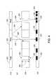
- FIGS. 7-11depict various embodiments of silicon image optical sensors that include features to enable high performance for use as a fingerprint sensor. These features include any of: 1) collimator filter structures above the light sensor elements (also referred to herein as optical sensor elements or sensing pixels) to restrict the acceptance angle of the incoming light (to facilitate precise imaging through thicknesses of material); 2) non-sense devices/circuit elements dispersed within the same layers as the optical sensing pixels to economize the silicon usage; 3) Light absorbing materials/coatings to reduce large angle light; 4) use of through silicon via (TSV) to connect the image sensor die and facilitate the use of back-side-illuminated (BSI) orientation; 5) optical sensing elements located to discriminate between low-angle and high-angle light; 6) use of two ASICS to enable modularity of features.
- TSVthrough silicon via
- BSIback-side-illuminated
- FIG. 7depicts an image sensor structure in accordance with the present disclosure.
- the sensor structure in FIG. 7is a CMOS optical fingerprint sensor including: wafer-scale integrated collimator filters ( 1 ); non-sense devices and circuit elements ( 2 ) co-planar with light sensing pixels or optical sensing elements ( 5 ) disposed in the area between the collimator apertures (behind a blocking portion of the collimator filter); light absorbing materials or coatings ( 3 ) to reduce large-angle light; through silicon via connection (TSV) ( 4 ) to facilitate a backside illumination (BSI) orientation for the image sensor; re-distribution layers ( 6 ); and an illustration of large angle ( ⁇ ) and low angle ( ⁇ ) light.
- TSVsilicon via connection
- BSIbackside illumination
- 6re-distribution layers
- collimator filterOne option for creating a collimator filter is to laser drill holes through a black mylar film, then place this film directly on top of the pixel sensor array of a CCD image sensor. When images are taken with the collimator filter in place, the raw images may require considerable reconstruction to convert them into the resolved images for the desired application. There are some drawbacks to this approach that make it less desirable for a practical consumer fingerprint sensor. For example, building the collimator filter as a separate film and attaching it creates the potential for many defects (e.g., misalignments, banding and/or missing pixels). It would be beneficial if these filters can be created using wafer-level processes to lower fabrication costs and reduce the possibilities for defects.
- the collimator filtermay only transmit light to a small fraction of the pixels in the image sensor. For example, with a 1000 dpi setup for the sensing pixels, a sense area of approximately 10 um in diameter for every 25 um, or roughly only 13% of the total area of the image sensor may be needed. This could result inefficient use of processed silicon or higher silicon fabrication costs than desired.
- FIGS. 7-17illustrate embodiments using backside illuminated (BSI) structures.
- FIGS. 8 and 9illustrate embodiments using frontside illuminated (FSI) structures.
- CMOS sensors todaythere are several constructions for ordinary image sensing applications.
- One such constructionis to form light pipes through the RDLs.
- FSIfront-side-illuminated
- the light detected by the image sensoris introduced on the RDL side and reaches the sensors through these light pipes.
- These light pipeshave many features that enhance the ability to collect all light at as large a range of angles as possible and efficiently deliver the photons to the sensor, including improving reflection on the side walls of the light pipes, and microlenses that are configured as converging optical elements.
- Another constructionis the Back-side-illuminated (BSI) construction, where light is introduced from the side opposite the RDLs.
- BSIBack-side-illuminated
- RDLsare built up on the front side as before, but without light pipes on this RDL side. Instead, the sensing pixels/optical sensing elements of the image sensor are exposed from the backside by thinning the wafer from the backside opposite the RDLs.
- Embodiments of this disclosureinclude image sensor structures that differ from ordinary image sensors in many respects to facilitate biometric feature (e.g., fingerprint) sensing.
- a “front side illuminated” (FSI) construction of the present disclosureas illustrated in FIGS. 8 and 9 , collimator filter apertures may be formed directly through redistribution layers (RDLs) built up on the front side of the image sensor.
- RDLsredistribution layers
- the collimator filter aperturesmay be fabricated directly into the bulk silicon. In FIGS. 7 and 11 , this is shown as selective etching of the backside of the image sensor wafer to form the collimator apertures, thus only exposing some of the pixels to the backside while leaving behind some of the image sensor wafer to act as a light blocking portion of the collimator filter.
- the sensing side (e.g., sensing region side) of the image sensor structurecorresponds to the side having the collimator apertures or holes.
- the sensing region (e.g., for a fingerprint input) for the image sensor structure in FIGS. 7 and 11corresponds to the bottom of these drawing sheets, while the sensing region for the image sensor structure in FIGS. 8 and 9 corresponds to the top of these drawing sheets.
- a BSI construction using through silicon viascan be used to connect an image sensor ASIC to a packaging substrate (PCB, etc.).
- a BSI constructioncan also use TSV to mount an image sensor ASIC to a second ASIC.
- This second ASICcould contain digital capability such as image processing, encryption, fingerprint matching capability, memory, etc.
- devices and circuitry ( 2 )can be added in the sensor layer of the image sensor die/wafer that is not needed for capturing incoming light. This can be added in the area of the image sensor blocked by the collimator filter.
- light which exits the collimator filtermay have a different radial distance from the center which will depend on the entrance angle of the light. It may be useful to segregate the pixel(s) under each hole to discriminate between light of a large angle from that of a small angle, (e.g., Diode Detector ( 2 ) and Diode Detector ( 1 ), respectively, as shown in FIG. 9 ).
- This disclosurealso describes various additional ways to fabricate a collimator layer with silicon (Si) wafers.
- Sisilicon
- thesemay be formed at the wafer level by attaching a collimator filter wafer to an image sensor wafer, as described below.
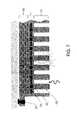
- FIG. 12An exemplary optical image sensor structure 1200 with a collimator filter layer 1205 , having an array of collimator filter apertures or holes, bonded to an image sensor layer 1210 is shown in FIG. 12 and general process steps for fabricating the same according to certain embodiments are shown in the FIGS. 13-18 .
- FIG. 13illustrates a process 1300 for fabricating a collimator filter layer 1205 according to an embodiment.
- a mask layer 1302is added to the polished side of a wafer substrate 1304 , e.g., single-side polished Si wafer.
- the mask layer 1302includes a mask material that should have significantly slower etch rate, compared to the wafer substrate (e.g., Si) etch rate.
- the mask layer 1302is patterned to form an etch mask 1306 defining a collimator hole pattern.
- photoresiste.g., a soft mask
- patterningcan be done with traditional lithography processes such as spin-coating, baking, exposure and development.
- other mask materialse.g., hard masks
- an additional layer of photoresistshould be applied on top of the hard mask to create patterns/holes in the mask layer with traditional lithography processes, followed by wet or dry etching of exposed areas in the etch mask.
- etch mask 1306 including the hole patternis created, in step 1330 ( FIG. 13C ), the frontside (F) of the wafer substrate 1304 is attached to a support structure 1308 1 (e.g., a UV tape) and thinned down from the backside (B) using conventional wafer thinning techniques.
- the target thicknessshould be determined based on the desired collimator filter hole size and the pitch.
- the target thickness(and hence the desired length or depth of the collimator holes) is generally between about 30 ⁇ m and about 300 ⁇ m, where an initial thickness of the wafer substrate is greater than about 500 ⁇ m, e.g., from about 500 ⁇ m up to about 1 mm or 2 mm.
- the wafer substrateis removed or detached from the support structure (e.g., UV tape) and, in step 1340 ( FIG. 13D ), attached to another support structure 1308 2 (e.g., a UV tape) on the backside (B), revealing the frontside (F) where the etch mask 1306 is located.
- the support structuree.g., UV tape
- step 1340FIG. 13D
- another support structure 1308 2e.g., a UV tape
- FIG. 14AAn example of a thinned-down wafer substrate attached to a UV tape 1308 2 (attached wafer substrate) is shown in FIG. 14A .
- the attached wafer substrateis etched to form collimator filter holes or vias in the wafer substrate 1304 .
- the attached wafer substratemay be placed in a Si DRIE (deep reactive ion etching, also known as “Bosch” process) equipment chamber to go through Si etching to make the holes or vias.
- the etchershould be equipped to handle the UV tape.
- One such etcheris the MicroDie SingulatorTM from Plasma-Therm, LLC.
- the vias from this DRIE stepcan be created straight down (see FIG.
- step 1360FIG. 13F
- the collimator filter wafercan be detached from the support structure 1308 2 .
- the detached collimator filter waferis then aligned with and attached (e.g., adhesive bonded) to an image sensor wafer to form an optical sensor wafer having a plurality of light collimating apertures or holes in the collimator filter layer aligned with a plurality of light sensing elements or pixels in the image sensor wafer.
- the image sensor waferis singulated to form a plurality of individual optical image sensor structures 1200 (e.g., individual optical biometric sensors), each having a plurality of light collimating apertures or holes in the collimator filter layer aligned with a plurality of light sensing elements or pixels.
- individual optical image sensor structures 1200e.g., individual optical biometric sensors
- Alignment marksshould exist on both the collimator filter wafer and the image sensor wafer. Based on the alignment marks on the image sensor wafer, new sets of alignment marks may be created when the collimator wafers are processed. In one embodiment, such fiduciary marks are created on the frontside of the wafer substrate as part of the etch mask patterning step 1320 and/or during the etching step 1350 .
- Wafer bonding systemshave several alignment techniques, and one of the alignment techniques that may be applied according to an embodiment is called “inter-substrate” alignment as shown in FIG. 15 .
- the camera(s)locate between the wafers and observe the alignment marks on the bottom of the upper wafer and on the top of the lower wafer. When it is confirmed that both wafers are aligned, the wafers are locked in place and ready for bonding. With this technique, 3D stacking such as die-to-wafer or wafer-to-wafer bonding becomes possible.
- Attachment of a collimator filter wafer to an image sensor wafercan be done, e.g., using wafer bonders from Suss MicroTec, EVG, Ayumi, etc., after alignment is completed. Both heat and pressure help to bond the wafers together. There are several bonding types (metal, oxide, eutectic, direct, etc.), and adhesive bonding is advantageous since no high temperature ( ⁇ 200 deg C.) is used, and no strict requirement exists regarding smoothness of the bonding surface.
- the image sensor waferis coated with adhesive and patterned to only cover the areas between the edge of the image sensor pixel area and the bond pads. The bond pads should not have anything on top to make wire bonding possible, unless TSV (through silicon via) is used to make connections between the image sensor and the PCB underneath.
- FIG. 16shows different scribe lines 1610 for the collimator filter wafer and the image sensor useful to remove substrate material (e.g., silicon) on top of bond pads 1618 of the image sensor.
- forming the collimator filter waferincludes forming a plurality of scribe line pairs 1616 , where each scribe line pair 1616 defines a removal region 1612 therebetween in the collimator filter wafer.
- the image sensor waferalso includes a pair of bond pads 1618 under each removal region 1612 of the collimator filter wafer.
- singulating the image sensor waferincludes removing each removal region 1616 in the collimator filter wafer between each scribe line pair 1616 , e.g., by half-cut dicing or by etching, to thereby expose each pair of bond pads 1618 (and scribe lines 1620 ) in the image sensor wafer. Singulating further includes dicing the image sensor wafer at the scribe line 1620 between each bond pad 1618 of each bond pad pair. If TSV is applied, removal of wafer substrate material above the image sensor scribe lines 1620 may not be needed and the same scribe line 1620 can be shared by both the collimator filter wafer and the image sensor wafer.
- a carrier wafermay also be used for mechanical stability and to preserve precise registration across a wafer.
- the individual per-die collimator hole fiduciary or alignment marksare etched using the same etch that is used for forming the collimator holes. This results in individual collimator filter layers (i.e. one collimator filter layer per image sensor die, with each collimator filter layer having an array of apertures), but the individual collimator filters may be attached to a carrier wafer that all may be bonded to the image sensor wafer in a wafer-wafer bond process.
- the collimator filter wafermay be partially etched during the etching, e.g. Si DRIE step, and thinning may occur after bonding to the image sensor wafer is completed, as illustrated in process 1700 of FIG. 17 .
- This alternate methodwill eliminate one support structure (e.g., UV tape) bonding step from the previously described process.
- a mask layer 1702is added to the polished side of a wafer substrate 1704 , e.g., single-side polished Si wafer.
- the mask layer 1702includes a mask material that should have significantly slower etch rate, compared to the wafer substrate (e.g., Si) etch rate.
- the mask layer 1702is patterned to form an etch mask 1706 defining the pattern of collimator holes.
- photoresiste.g., a soft mask
- patterningcan be done with traditional lithography processes such as spin-coating, baking, exposure and development.
- other mask materialse.g., hard masks
- an additional layer of photoresistshould be applied on top of the hard mask to create patterns/holes with traditional lithography processes, followed by wet or dry etching of exposed areas in the etch mask.
- etch mask 1706 including the hole patternis created, the backside (B) of the wafer substrate 1704 is attached to a support structure 1708 , e.g., a UV tape, (attached wafer substrate).
- support structure 1708is not needed and is not used (e.g., depending on the etcher tool used).
- the wafer substratee.g., attached wafer substrate
- the wafer substrateis partially etched to form collimator filter holes or vias extending partially through the wafer substrate 1704 to a target depth less than the thickness of the substrate wafer.
- the wafer substratemay be placed in a Si DRIE (deep reactive ion etching, also known as “Bosch” process) equipment chamber to go through Si etching to make the partial holes or vias.
- a Si DRIEdeep reactive ion etching, also known as “Bosch” process
- the etchershould be equipped to handle the UV tape.
- One such etcheris the MicroDie SingulatorTM from Plasma-Therm, LLC.
- the target thicknessshould be determined based on the desired collimator filter hole size and the pitch.
- the desired length or depth of the collimator holes to be formedis between about 30 ⁇ m and about 300 ⁇ m, so the target depth of the partially etched collimator holes should be at least the same as or greater than the desired length or depth of the collimator holes to be formed.
- the initial thickness of the wafer substrateis greater than about 500 ⁇ m, e.g., from about 500 ⁇ m up to about 1 mm or 2 mm.
- the partially etched wafer substrateis detached from the support structure 1708 .
- the frontside of the wafer substrate(including partially etched collimator holes) is aligned with and attached (e.g., adhesive bonded) to an image sensor wafer. Examples of alignment and bonding techniques are discussed above.
- the mask layer 1706may be kept or removed prior to bonding to the image sensor wafer.
- step 1750( FIG. 17D ).
- the backside (B)is thinned down using conventional wafer thinning techniques to expose the plurality of partially etched holes or vias to form a collimator filter layer on the image sensor wafer, wherein the exposed holes or vias correspond to the plurality of light collimating apertures or holes.
- the resulting wafer structure, including a collimator filter layer on the image sensor wafer,may be singulated to produce a plurality of optical biometric sensor devices.
- FIG. 18depicts another process 1800 of forming an image sensor wafer structure with a collimator filter layer in accordance with an embodiment.
- a wafer substrateis bonded to a carrier wafer, or carrier substrate, and then thinned to a desired thickness in step 1820 ( FIG. 18B ).
- the carrier waferprovides additional structural support to enhance processing capabilities of the substrate wafer (e.g., a thinner wafer) using various wafer processing tools.
- a mask layeris added to the exposed side of the wafer substrate.
- the mask layerincludes a mask material that should have significantly slower etch rate, compared to the wafer substrate (e.g., Si) etch rate.
- the mask layeris patterned to form an etch mask defining the collimator holes pattern.
- photoresiste.g., a soft mask
- patterningcan be done with traditional lithography processes such as spin-coating, baking, exposure and development.
- other mask materialse.g., hard masks
- an additional layer of photoresistshould be applied on top of the hard mask to create patterns/holes with traditional lithography processes, followed by wet or dry etching of exposed areas in the etch mask.
- the collimator holesare formed by etching all-the-way through the wafer substrate. Additionally, the dicing of individual collimator die structures can be achieved during this etch step in one embodiment.
- the maske.g., hard mask
- the wafer substrate, including the etched collimator holesis bonded to an image sensor wafer, e.g., CMOS wafer, using a wafer-to-wafer bonding process as discussed above.
- the carrier waferis released from the (collimator) wafer substrate to reveal individual collimators precisely bonded to the image sensors, e.g., CMOS image sensors.
- this inventiondescribes optical object imaging in the context of fingerprint image sensing, the method and system may be used to image other objects as well.
- a high resolution image of a palm or handmay be acquired by placing the hand directly on the cover layer. Imaging of non-biometric objects is also with the scope of this disclosure.
- collimatorin the text of collimator filter holes or hole structures does not imply that light rays entering a collimator filter hole are actively collimated (e.g., made parallel).
- the collimator filter holesgenerally allow light rays entering to pass through without deviation or alteration (unless a light ray interacts with a sidewall of the collimator filter hole, in which case the light ray may be reflected or absorbed, partially or entirely, depending on the characteristics of the sidewall).
Landscapes
- Physics & Mathematics (AREA)
- Engineering & Computer Science (AREA)
- General Physics & Mathematics (AREA)
- Optics & Photonics (AREA)
- Human Computer Interaction (AREA)
- Multimedia (AREA)
- Theoretical Computer Science (AREA)
- Image Input (AREA)
- Solid State Image Pick-Up Elements (AREA)
Abstract
Description
Claims (17)
Priority Applications (6)
| Application Number | Priority Date | Filing Date | Title |
|---|---|---|---|
| US15/087,481US10147757B2 (en) | 2015-02-02 | 2016-03-31 | Image sensor structures for fingerprint sensing |
| KR1020187012976AKR102439203B1 (en) | 2015-10-07 | 2016-10-05 | Image sensor structures for fingerprint sensing |
| PCT/US2016/055574WO2017062506A1 (en) | 2015-10-07 | 2016-10-05 | Image sensor structures for fingerprint sensing |
| CN201680065199.3ACN108352396B (en) | 2015-10-07 | 2016-10-05 | Image sensor structure for fingerprint sensing |
| EP16854251.2AEP3360162B1 (en) | 2015-10-07 | 2016-10-05 | Image sensor structures for fingerprint sensing |
| JP2018517294AJP2018537845A (en) | 2015-10-07 | 2016-10-05 | Image sensor structure for fingerprint detection |
Applications Claiming Priority (4)
| Application Number | Priority Date | Filing Date | Title |
|---|---|---|---|
| US201562111012P | 2015-02-02 | 2015-02-02 | |
| US14/871,810US9829614B2 (en) | 2015-02-02 | 2015-09-30 | Optical sensor using collimator |
| US201562238603P | 2015-10-07 | 2015-10-07 | |
| US15/087,481US10147757B2 (en) | 2015-02-02 | 2016-03-31 | Image sensor structures for fingerprint sensing |
Related Parent Applications (1)
| Application Number | Title | Priority Date | Filing Date |
|---|---|---|---|
| US14/871,810Continuation-In-PartUS9829614B2 (en) | 2015-02-02 | 2015-09-30 | Optical sensor using collimator |
Publications (2)
| Publication Number | Publication Date |
|---|---|
| US20160254312A1 US20160254312A1 (en) | 2016-09-01 |
| US10147757B2true US10147757B2 (en) | 2018-12-04 |
Family
ID=56798393
Family Applications (1)
| Application Number | Title | Priority Date | Filing Date |
|---|---|---|---|
| US15/087,481Active2035-11-25US10147757B2 (en) | 2015-02-02 | 2016-03-31 | Image sensor structures for fingerprint sensing |
Country Status (1)
| Country | Link |
|---|---|
| US (1) | US10147757B2 (en) |
Cited By (14)
| Publication number | Priority date | Publication date | Assignee | Title |
|---|---|---|---|---|
| US20190087627A1 (en)* | 2016-03-16 | 2019-03-21 | Shanghai Oxi Technology Co., Ltd. | Optical Fingerprint Module |
| US20190122025A1 (en)* | 2017-10-20 | 2019-04-25 | Synaptics Incorporated | Optical biometric sensor with automatic gain and exposure control |
| CN109993149A (en)* | 2019-04-12 | 2019-07-09 | 京东方科技集团股份有限公司 | Terminals, display panels and fingerprint recognition modules |
| US10360432B1 (en)* | 2018-02-23 | 2019-07-23 | Shenzhen GOODIX Technology Co., Ltd. | Optical imaging via imaging lens and imaging pinhole in under-screen optical sensor module for on-screen fingerprint sensing in devices having organic light emitting diode (OLED) screens or other screens |
| CN110133892A (en)* | 2019-05-31 | 2019-08-16 | 厦门天马微电子有限公司 | The manufacturing method of display panel, display device and display panel |
| US20190303638A1 (en)* | 2018-03-28 | 2019-10-03 | Shanghai Tianma Micro-electronics Co., Ltd. | Display Panel And Display Device |
| US10628656B2 (en)* | 2015-07-09 | 2020-04-21 | Gingy Technology Inc. | Image capture apparatus |
| US10691914B2 (en)* | 2017-09-28 | 2020-06-23 | Primax Electronics Ltd | Optical fingerprint sensing unit and manufacturing method thereof |
| US10726240B2 (en)* | 2015-07-09 | 2020-07-28 | Gingy Technology Inc. | Image capturing apparatus |
| US10789443B2 (en)* | 2018-01-03 | 2020-09-29 | Boe Technology Group Co., Ltd. | Recognition device, fingerprint recognition device and fingerprint recognition apparatus |
| US20200393313A1 (en)* | 2019-06-17 | 2020-12-17 | The Hong Kong University Of Science And Technology | Tactile sensors and methods |
| US11048306B2 (en)* | 2018-01-08 | 2021-06-29 | Samsung Electronics Co., Ltd. | Electronic device including sensor for generating image data using incident light through opening formed in display |
| US20230351798A1 (en)* | 2022-04-27 | 2023-11-02 | Omnivision Technologies, Inc. | Fingerprint sensor with wafer-bonded microlens array |
| US12261970B2 (en) | 2019-02-19 | 2025-03-25 | Samsung Electronics Co., Ltd. | Method for manufacturing display module comprising sensor, and electronic device comprising display module |
Families Citing this family (65)
| Publication number | Priority date | Publication date | Assignee | Title |
|---|---|---|---|---|
| US8906320B1 (en) | 2012-04-16 | 2014-12-09 | Illumina, Inc. | Biosensors for biological or chemical analysis and systems and methods for same |
| US9606068B2 (en)* | 2014-08-27 | 2017-03-28 | Pacific Biosciences Of California, Inc. | Arrays of integrated analytical devices |
| US10732771B2 (en) | 2014-11-12 | 2020-08-04 | Shenzhen GOODIX Technology Co., Ltd. | Fingerprint sensors having in-pixel optical sensors |
| TW201640418A (en) | 2015-05-04 | 2016-11-16 | 曦威科技股份有限公司 | Fingerprint detecting device, mobile device using the same, and manufacturing method thereof |
| US10437974B2 (en) | 2015-06-18 | 2019-10-08 | Shenzhen GOODIX Technology Co., Ltd. | Optical sensing performance of under-screen optical sensor module for on-screen fingerprint sensing |
| CN107580709B (en) | 2015-06-18 | 2021-02-12 | 深圳市汇顶科技股份有限公司 | Multifunctional fingerprint sensor with optical sensing capability |
| CN107004130B (en) | 2015-06-18 | 2020-08-28 | 深圳市汇顶科技股份有限公司 | Optical sensor module under screen for sensing fingerprint on screen |
| US10410037B2 (en) | 2015-06-18 | 2019-09-10 | Shenzhen GOODIX Technology Co., Ltd. | Under-screen optical sensor module for on-screen fingerprint sensing implementing imaging lens, extra illumination or optical collimator array |
| US10410033B2 (en) | 2015-06-18 | 2019-09-10 | Shenzhen GOODIX Technology Co., Ltd. | Under-LCD screen optical sensor module for on-screen fingerprint sensing |
| CN107004126A (en) | 2015-11-02 | 2017-08-01 | 深圳市汇顶科技股份有限公司 | Multifunctional fingerprint sensor with anti-fingerprint spoofing optical sensing |
| CN107203737A (en)* | 2016-03-17 | 2017-09-26 | 台瀚科技股份有限公司 | Thin fingerprint identification device with optical film |
| US20180039811A1 (en)* | 2016-08-05 | 2018-02-08 | Gingy Technology Inc. | Biometric apparatus |
| US10332929B2 (en)* | 2016-09-07 | 2019-06-25 | Mei-Yen Lee | Integrated sensing module and integrated sensing assembly using the same |
| CN109983369B (en)* | 2016-11-22 | 2022-03-08 | 3M创新有限公司 | Angle and Spectral Selective Detector and Light Source System |
| US10055637B2 (en)* | 2016-12-07 | 2018-08-21 | Synaptics Incorporated | Optical sensor with substrate light filter |
| FR3060811A1 (en) | 2016-12-19 | 2018-06-22 | New Imaging Technologies | DEVICE FOR ACQUIRING DIGITAL IMPRESSIONS |
| CN108241828A (en)* | 2016-12-23 | 2018-07-03 | 创智能科技股份有限公司 | Biometric identification device |
| EP3440594A4 (en)* | 2017-01-04 | 2019-09-25 | Shenzhen Goodix Technology Co., Ltd. | ENHANCING OPTICAL DETECTION PERFORMANCE OF OPTICAL SENSOR MODULE SUB-SCREEN FOR DIGITAL FOOTPRINT DETECTION ON SCREEN |
| CN106886753B (en)* | 2017-01-16 | 2020-12-15 | 业泓科技(成都)有限公司 | Electronic device using acoustic wave type fingerprint identification device |
| WO2018133768A1 (en)* | 2017-01-17 | 2018-07-26 | 苏州晶方半导体科技股份有限公司 | Packaging structure and packaging method for fingerprint recognition chip |
| US10388689B2 (en) | 2017-02-13 | 2019-08-20 | Egis Technology Inc. | Fingerprint identification system, sensing method and manufacturing method |
| CN106886767B (en)* | 2017-02-23 | 2019-07-05 | 京东方科技集团股份有限公司 | A kind of optical fingerprint identification device and display panel |
| US10614283B2 (en) | 2017-03-07 | 2020-04-07 | Shenzhen GOODIX Technology Co., Ltd. | Devices with peripheral task bar display zone and under-LCD screen optical sensor module for on-screen fingerprint sensing |
| WO2018164634A1 (en)* | 2017-03-10 | 2018-09-13 | Fingerprint Cards Ab | Fingerprint sensor module and a method for manufacturing such a fingerprint sensor module |
| EP3425557B1 (en)* | 2017-04-06 | 2021-03-31 | Shenzhen Goodix Technology Co., Ltd. | Manufacturing method of a fingerprint identification device |
| CN110096928B (en)* | 2018-01-30 | 2021-08-06 | 京东方科技集团股份有限公司 | Fingerprint identification device and display device |
| US11373386B2 (en)* | 2017-04-17 | 2022-06-28 | Boe Technology Group Co., Ltd. | Pattern identification device and display apparatus |
| CN107092311B (en)* | 2017-04-27 | 2020-03-03 | Oppo广东移动通信有限公司 | Display screen, display device and mobile terminal |
| DE202018006696U1 (en)* | 2017-05-15 | 2022-04-01 | Ouster, Inc. | Optical image transmitter with brightness improvement |
| TWI639022B (en) | 2017-05-18 | 2018-10-21 | 吳志彥 | Optical element fabrication method and optical sensing device |
| CN107103307B (en)* | 2017-05-23 | 2020-05-22 | 京东方科技集团股份有限公司 | Touch Panels and Display Devices |
| CN107222592A (en)* | 2017-05-25 | 2017-09-29 | 维沃移动通信有限公司 | A kind of control method of mobile terminal and mobile terminal |
| CN108684207A (en) | 2017-06-13 | 2018-10-19 | 深圳市汇顶科技股份有限公司 | Optical bio identifies module, display device and electronic equipment |
| CN109145702A (en) | 2017-06-15 | 2019-01-04 | 神盾股份有限公司 | Optical fingerprint sensor |
| WO2018227514A1 (en)* | 2017-06-16 | 2018-12-20 | 深圳市汇顶科技股份有限公司 | Fingerprint image processing method, optical fingerprint recognition system, and electronic device |
| KR102400628B1 (en)* | 2017-08-17 | 2022-05-23 | 삼성전자주식회사 | Electronic device and display for reducing leakage current |
| CN107958196B (en)* | 2017-08-17 | 2021-06-22 | 深圳信炜科技有限公司 | Photosensitive chips and electronic equipment |
| CN209803814U (en)* | 2017-08-17 | 2019-12-17 | 深圳信炜科技有限公司 | photosensitive chip and electronic equipment |
| DE102017119983B3 (en)* | 2017-08-31 | 2018-09-27 | JENETRIC GmbH | Apparatus for contact-based simultaneous recording of autopod impressions |
| CN107655565A (en)* | 2017-09-19 | 2018-02-02 | 京东方科技集团股份有限公司 | Determine the method, apparatus and equipment of intensity of illumination |
| US10395620B2 (en)* | 2017-09-22 | 2019-08-27 | Apple Inc. | Electronic devices having ambient light sensors with light collimators |
| KR102403015B1 (en)* | 2017-09-29 | 2022-05-27 | 삼성전자주식회사 | Electronic device with fingerprint scan sensor |
| US10796128B2 (en)* | 2017-12-12 | 2020-10-06 | Fingerprint Cards Ab | Optical sensor with ambient light filter |
| US10861829B2 (en)* | 2017-12-26 | 2020-12-08 | Illumina, Inc. | Sensor system |
| TWI667802B (en)* | 2018-02-05 | 2019-08-01 | 世界先進積體電路股份有限公司 | Optical sensor and the manufacturing method thereof |
| CN110164882B (en)* | 2018-02-11 | 2021-11-12 | 世界先进积体电路股份有限公司 | Optical sensor and method for manufacturing the same |
| US10303921B1 (en)* | 2018-02-26 | 2019-05-28 | Shenzhen GOODIX Technology Co., Ltd. | On-LCD screen optical fingerprint sensing based on optical imaging with lens-pinhole module and other optical designs |
| CN108399392B (en)* | 2018-03-07 | 2021-01-26 | 京东方科技集团股份有限公司 | Fingerprint identification structure and display device |
| EP3766003A4 (en) | 2018-03-15 | 2021-05-12 | Fingerprint Cards AB | Biometric imaging device and method for manufacturing a biometric imaging device |
| DE102018208650A1 (en)* | 2018-05-30 | 2019-12-05 | Infineon Technologies Dresden Gmbh | SENSOR ARRANGEMENT, PARTICLE SENSOR AND METHOD FOR MANUFACTURING A SENSOR ARRANGEMENT |
| CN108960208B (en)* | 2018-08-09 | 2021-03-02 | 京东方科技集团股份有限公司 | Light collimation structure and manufacturing method thereof and optical fingerprint identification device |
| TWI677079B (en)* | 2018-08-30 | 2019-11-11 | 精材科技股份有限公司 | Chip package and manufacturing method thereof |
| WO2020118620A1 (en) | 2018-12-13 | 2020-06-18 | 深圳市汇顶科技股份有限公司 | Fingerprint recognition apparatus and method, and electronic device |
| KR102808360B1 (en)* | 2019-01-04 | 2025-05-19 | 삼성디스플레이 주식회사 | Fingerprint sensor and display device including the same |
| CN208848221U (en)* | 2019-04-10 | 2019-05-10 | 深圳市汇顶科技股份有限公司 | Optical fingerprint identification devices and electronic equipment |
| WO2020215292A1 (en)* | 2019-04-25 | 2020-10-29 | 深圳市汇顶科技股份有限公司 | Optical fingerprint recognition apparatus, electronic device and fingerprint recognition method |
| CN110321832B (en)* | 2019-06-28 | 2021-05-18 | 维沃移动通信有限公司 | Optical module and mobile terminal |
| CN112699866B (en)* | 2019-10-22 | 2025-01-07 | 世界先进积体电路股份有限公司 | Semiconductor device and method of forming the same |
| EP3839808B1 (en)* | 2019-11-01 | 2023-09-20 | Shenzhen Goodix Technology Co., Ltd. | Fingerprint detection apparatus and electronic device |
| CN211857087U (en)* | 2020-02-24 | 2020-11-03 | 宁波激智科技股份有限公司 | Interference reducing collimation film |
| JP7365964B2 (en)* | 2020-05-21 | 2023-10-20 | 株式会社ジャパンディスプレイ | Detection device and display device |
| CN113707678B (en)* | 2020-05-22 | 2023-09-22 | 格科微电子(上海)有限公司 | Optical fingerprint device and manufacturing method thereof |
| KR20220083915A (en) | 2020-12-11 | 2022-06-21 | 삼성디스플레이 주식회사 | Display appatus inculding the detection sensor and method for manufacturing the detection sensor |
| US12266208B2 (en)* | 2021-07-07 | 2025-04-01 | Tianjin Jiiov Technology Co., Ltd. | Biometric information recognition module and electronic device |
| WO2024117969A1 (en)* | 2022-12-02 | 2024-06-06 | Advanced Micro Foundry Pte. Ltd. | Optical beam receiver assembly |
Citations (89)
| Publication number | Priority date | Publication date | Assignee | Title |
|---|---|---|---|---|
| US5446290A (en) | 1993-05-13 | 1995-08-29 | Nec Corporation | Fingerprint image input device having an image sensor with openings |
| US5726443A (en) | 1996-01-18 | 1998-03-10 | Chapman Glenn H | Vision system and proximity detector |
| US5991467A (en) | 1996-07-18 | 1999-11-23 | Alps Electric Co., Ltd. | Image reading apparatus containing light receiving transistors and switching transistors |
| US6128399A (en) | 1996-03-28 | 2000-10-03 | Sagem Sa | Fingerprint sensor device |
| US20020054394A1 (en) | 1998-03-12 | 2002-05-09 | Casio Computer Co., Ltd | Reading apparatus for reading fingerprint |
| US20030090650A1 (en)* | 2001-11-09 | 2003-05-15 | Nec Corporation | Fingerprint input devices and electronic devices provided with the same |
| CN1451205A (en) | 1999-12-18 | 2003-10-22 | 株式会社利真 | Information terminal with buil t-in fingerprint recognizer |
| US20040252867A1 (en) | 2000-01-05 | 2004-12-16 | Je-Hsiung Lan | Biometric sensor |
| US20060113622A1 (en)* | 2004-11-30 | 2006-06-01 | International Business Machines Corporation | A damascene copper wiring image sensor |
| US20060152615A1 (en) | 2005-01-07 | 2006-07-13 | Yong-Chai Kwon | Image sensor chip having plate, wafer assembly and manufacturing method for the same |
| US20070290284A1 (en)* | 2006-06-19 | 2007-12-20 | Jamie Lyn Shaffer | Incident light angle detector for light sensitive integrated circuit |
| US20080121442A1 (en) | 2006-11-27 | 2008-05-29 | Microsoft Corporation | Infrared sensor integrated in a touch panel |
| US20080237766A1 (en)* | 2005-02-02 | 2008-10-02 | Ki-Hong Kim | Image sensing devices including image sensor chips, image sensor package modules employing the image sensing devices, electronic products employing the image sensor package modules, and methods of fabricating the same |
| US7465914B2 (en) | 2003-09-12 | 2008-12-16 | Flatfrog Laboratories Ab | System and method of determining a position of a radiation scattering/reflecting element |
| US20090080709A1 (en)* | 2006-07-19 | 2009-03-26 | Lumidigm, Inc. | Whole-Hand Multispectral Biometric Imaging |
| US7535468B2 (en) | 2004-06-21 | 2009-05-19 | Apple Inc. | Integrated sensing display |
| US20100067757A1 (en)* | 2008-09-16 | 2010-03-18 | Shinichi Arai | Image acquisition apparatus and biometric information acquisition apparatus |
| US7697053B2 (en) | 2006-11-02 | 2010-04-13 | Eastman Kodak Company | Integrated display having multiple capture devices |
| US7728959B2 (en) | 2003-06-21 | 2010-06-01 | Aprilis, Inc. | Acquisition of high resolution biometric images |
| US20100172552A1 (en) | 2009-01-07 | 2010-07-08 | Jen-Chieh Wu | Fingerprint indentifying system |
| US20100183200A1 (en) | 2009-01-16 | 2010-07-22 | Jen-Chieh Wu | Fingerprint Input Module |
| US20100204064A1 (en)* | 2009-02-11 | 2010-08-12 | Samsung Electronics Co., Ltd. | Integrated bio-chip and method of fabricating the integrated bio-chip |
| US20100208952A1 (en) | 2009-02-19 | 2010-08-19 | Jew-Chieh Wu | Fingerprint indentifying system |
| US20100208954A1 (en) | 2009-02-19 | 2010-08-19 | Jen-Chieh Wu | Fingerprint identifying system |
| CN101814126A (en) | 2009-02-25 | 2010-08-25 | 金佶科技有限公司 | Optical fingerprint identification system |
| CN101814125A (en) | 2009-02-25 | 2010-08-25 | 金佶科技有限公司 | Optical fingerprint identification system |
| US20100283756A1 (en) | 2009-05-06 | 2010-11-11 | Ja-Seung Ku | Method and apparatus for recognizing touch |
| US7920130B2 (en) | 2007-07-18 | 2011-04-05 | Quanta Computer Inc. | Electronic apparatus equipped with touch panel capable of identifying fingerprint |
| TW201115479A (en) | 2009-10-23 | 2011-05-01 | Gingy Technology Inc | Light guide module for increasing image contrast |
| CN102073860A (en) | 2010-12-06 | 2011-05-25 | 清华大学 | Optical fingerprint acquisition device, optical fingerprint identification system and method |
| US20110122071A1 (en) | 2009-11-24 | 2011-05-26 | Microsoft Corporation | Angularly-selective sensor-in-pixel image detection |
| US20110233383A1 (en) | 2010-03-24 | 2011-09-29 | Hitachi Displays, Ltd. | Imaging apparatus |
| US20120076370A1 (en) | 2010-09-29 | 2012-03-29 | Lei Chih-Chi | Sectional image recognition method and zonal recognition device thereof |
| EP2447883A1 (en) | 2010-10-28 | 2012-05-02 | Gingy Technology, Inc. | Optical fingerprint recognition system |
| JP3177550U (en) | 2011-08-05 | 2012-08-09 | 金佶科技股▲ふん▼有限公司 | Finger rest |
| TWM435680U (en) | 2012-02-15 | 2012-08-11 | Gingy Technology Inc | Object motion detector |
| CN102682280A (en) | 2009-02-25 | 2012-09-19 | 金佶科技股份有限公司 | Optical fingerprint identification system |
| US8311514B2 (en) | 2010-09-16 | 2012-11-13 | Microsoft Corporation | Prevention of accidental device activation |
| US20120321149A1 (en) | 2011-05-17 | 2012-12-20 | Carver John F | Fingerprint sensors |
| CN202632318U (en) | 2012-03-19 | 2012-12-26 | 金佶科技股份有限公司 | fingerprint acquisition device |
| CN102842026A (en) | 2011-06-24 | 2012-12-26 | 金佶科技股份有限公司 | Fingerprint identification device |
| EP2562683A1 (en) | 2011-08-24 | 2013-02-27 | Gingy Technology, Inc. | Substrate for fingerprint contact |
| US20130120760A1 (en) | 2011-11-11 | 2013-05-16 | Daniel H. Raguin | Ambient light rejection for non-imaging contact sensors |
| US20130119237A1 (en) | 2011-11-12 | 2013-05-16 | Daniel H. Raguin | Ambient light illumination for non-imaging contact sensors |
| US20130169780A1 (en) | 2012-01-04 | 2013-07-04 | Gingy Technology Inc. | Method and device for dual lens fingerprint identification |
| US20130222282A1 (en) | 2012-02-29 | 2013-08-29 | Far Eastern New Century Corporation | Structure of Wet-coating Transparent Conductive Film and the Application Thereof |
| US8570303B2 (en) | 2008-09-04 | 2013-10-29 | Au Optronics Corporation | Display module |
| US20140125788A1 (en) | 2012-11-02 | 2014-05-08 | Gingy Technology Inc. | Fingerprint image capturing system |
| US8782775B2 (en) | 2007-09-24 | 2014-07-15 | Apple Inc. | Embedded authentication systems in an electronic device |
| CN103942537A (en) | 2014-04-04 | 2014-07-23 | 王曙光 | Liquid crystal terminal device, fingerprint image collection method and fingerprint collector |
| US20140218327A1 (en) | 2012-04-29 | 2014-08-07 | Weidong Shi | Method and Apparatuses of Transparent Fingerprint Imager Integrated with Touch Display Device |
| CN104035620A (en) | 2014-06-20 | 2014-09-10 | 深圳印象认知技术有限公司 | Optical sensing key, touch screen, fingerprint collecting device and electronic device |
| CN203838722U (en) | 2014-04-04 | 2014-09-17 | 深圳印象认知技术有限公司 | Liquid crystal terminal equipment and fingerprint acquisition device |
| TW201441940A (en) | 2013-04-24 | 2014-11-01 | Gingy Technology Inc | Fingerprint image capturing device |
| CN104182727A (en) | 2014-05-16 | 2014-12-03 | 深圳印象认知技术有限公司 | Ultra-thin fingerprint and palm print collection device, and fingerprint and palm print collection method |
| US20140355846A1 (en) | 2014-06-05 | 2014-12-04 | Secugen Corporation | Fingerprint Sensing Apparatus |
| CN204028936U (en) | 2014-05-16 | 2014-12-17 | 深圳印象认知技术有限公司 | Ultrathin fingerprint acquisition device, the display device of fingerprint can be gathered |
| US8921473B1 (en) | 2004-04-30 | 2014-12-30 | Sydney Hyman | Image making medium |
| TW201506807A (en) | 2013-08-15 | 2015-02-16 | Gingy Technology Inc | Identification method and identification device for authentic fingerprint |
| US20150062088A1 (en) | 2009-06-18 | 2015-03-05 | Au Optronics Corp. | Optical touch device and method of forming photo sensor |
| US20150078633A1 (en) | 2013-09-17 | 2015-03-19 | Gingy Technology Inc. | Method for determining fingerprint authenticity and device for the same |
| CN104463074A (en) | 2013-09-12 | 2015-03-25 | 金佶科技股份有限公司 | Method and device for identifying authenticity of fingerprint |
| WO2015041459A1 (en) | 2013-09-17 | 2015-03-26 | 실리콘 디스플레이 (주) | Optical fingerprint sensor |
| US20150109214A1 (en) | 2013-10-22 | 2015-04-23 | Weidong Shi | Methods and Apparatuses of touch-fingerprinting Display |
| US20150187827A1 (en) | 2013-12-26 | 2015-07-02 | Taiwan Semiconductor Manufacturing Company Ltd. | Semiconductor device and manufacturing method thereof |
| WO2015140600A1 (en) | 2014-03-21 | 2015-09-24 | Sony Corporation | Electronic device with display-based fingerprint reader |
| US9177190B1 (en) | 2014-05-30 | 2015-11-03 | Cheng Uei Precision Industry Co., Ltd. | Fingerprint sensor module |
| US20150331508A1 (en) | 2014-05-16 | 2015-11-19 | Apple Inc. | Integrated silicon-oled display and touch sensor panel |
| US20150347812A1 (en) | 2014-05-30 | 2015-12-03 | Egis Technology Inc. | Electronic device and fingerprint recognition method |
| US20150347813A1 (en) | 2014-05-28 | 2015-12-03 | Pacing Technology Co., Ltd. | Fingerprint image capturing device and fingerprint image capturing module thereof |
| US9208394B2 (en) | 2005-09-05 | 2015-12-08 | Alpvision S.A. | Authentication of an article of manufacture using an image of the microstructure of it surface |
| US20150371074A1 (en) | 2014-06-23 | 2015-12-24 | Shanghai Oxi Technology Co., Ltd. | Integrated optical sensor and methods for manufacturing and using the same |
| US20150371075A1 (en) | 2014-06-23 | 2015-12-24 | Shanghai Oxi Technology Co., Ltd | Array sensor apparatus and forming method thereof |
| US20150369661A1 (en) | 2014-06-23 | 2015-12-24 | Shanghai Oxi Technology Co., Ltd | Multi-purpose Thin Film Optoelectric Sensor |
| US20160092717A1 (en) | 2014-09-29 | 2016-03-31 | Shanghai Oxi Technology Co., Ltd | Information Detection and Display Apparatus, and Detecting Method and Displaying Method Thereof |
| US20160132712A1 (en)* | 2014-11-12 | 2016-05-12 | Shenzhen Huiding Technology Co., Ltd. | Fingerprint sensors having in-pixel optical sensors |
| WO2016119492A1 (en) | 2015-01-29 | 2016-08-04 | 深圳印象认知技术有限公司 | Fingerprint and palm print image collector with honeycomb structure, and terminal device |
| US20160247010A1 (en) | 2015-02-22 | 2016-08-25 | Microsoft Technology Licensing, Llc | Fingerprint Detection with Transparent Cover |
| US20160246396A1 (en) | 2015-02-20 | 2016-08-25 | Qualcomm Incorporated | Interactive touchscreen and sensor array |
| US9437132B2 (en) | 2011-11-30 | 2016-09-06 | Apple Inc. | Devices and methods for providing access to internal component |
| WO2016154378A1 (en) | 2015-03-25 | 2016-09-29 | Cressputi Research Llc | Electronic device including pin hole array mask above optical image sensor and related methods |
| US20160328595A1 (en)* | 2015-05-04 | 2016-11-10 | Eosmem Corporation | Fingerprint Detection Apparatus, Mobile Device Using the Same and Manufacturing Method Thereof |
| US9754150B2 (en) | 2015-07-09 | 2017-09-05 | Gingy Technology Inc. | Fingerprint identification module |
| US20170257534A1 (en) | 2016-03-07 | 2017-09-07 | Microsoft Technology Licensing, Llc | Pixel having a photoemitter and a photodetector triggered by a pixel selector signal bus |
| US20170279948A1 (en) | 2016-03-24 | 2017-09-28 | Motorola Mobility Llc | Embedded active matrix organic light emitting diode (amoled) fingerprint sensor |
| US20170300736A1 (en) | 2016-04-19 | 2017-10-19 | Samsung Electronics Co., Ltd. | Electronic device supporting fingerprint verification and method for operating the same |
| US20170316250A1 (en) | 2016-04-27 | 2017-11-02 | Samsung Electronics Co., Ltd. | Fingerprint verification method and electronic device for performing the same |
| US9818017B2 (en) | 2015-07-09 | 2017-11-14 | Gingy Technology Inc. | Fingerprint identification module |
| WO2017202323A1 (en) | 2016-05-25 | 2017-11-30 | 深圳印象认知技术有限公司 | Photosensitive image element, image collector, fingerprint collection device, and display device |
- 2016
- 2016-03-31USUS15/087,481patent/US10147757B2/enactiveActive
Patent Citations (145)
| Publication number | Priority date | Publication date | Assignee | Title |
|---|---|---|---|---|
| US5446290A (en) | 1993-05-13 | 1995-08-29 | Nec Corporation | Fingerprint image input device having an image sensor with openings |
| US5726443A (en) | 1996-01-18 | 1998-03-10 | Chapman Glenn H | Vision system and proximity detector |
| US6128399A (en) | 1996-03-28 | 2000-10-03 | Sagem Sa | Fingerprint sensor device |
| US5991467A (en) | 1996-07-18 | 1999-11-23 | Alps Electric Co., Ltd. | Image reading apparatus containing light receiving transistors and switching transistors |
| US20020054394A1 (en) | 1998-03-12 | 2002-05-09 | Casio Computer Co., Ltd | Reading apparatus for reading fingerprint |
| CN1451205A (en) | 1999-12-18 | 2003-10-22 | 株式会社利真 | Information terminal with buil t-in fingerprint recognizer |
| US20040252867A1 (en) | 2000-01-05 | 2004-12-16 | Je-Hsiung Lan | Biometric sensor |
| US20030090650A1 (en)* | 2001-11-09 | 2003-05-15 | Nec Corporation | Fingerprint input devices and electronic devices provided with the same |
| US7728959B2 (en) | 2003-06-21 | 2010-06-01 | Aprilis, Inc. | Acquisition of high resolution biometric images |
| US7465914B2 (en) | 2003-09-12 | 2008-12-16 | Flatfrog Laboratories Ab | System and method of determining a position of a radiation scattering/reflecting element |
| US8921473B1 (en) | 2004-04-30 | 2014-12-30 | Sydney Hyman | Image making medium |
| US7535468B2 (en) | 2004-06-21 | 2009-05-19 | Apple Inc. | Integrated sensing display |
| US20060113622A1 (en)* | 2004-11-30 | 2006-06-01 | International Business Machines Corporation | A damascene copper wiring image sensor |
| US20060152615A1 (en) | 2005-01-07 | 2006-07-13 | Yong-Chai Kwon | Image sensor chip having plate, wafer assembly and manufacturing method for the same |
| US20080237766A1 (en)* | 2005-02-02 | 2008-10-02 | Ki-Hong Kim | Image sensing devices including image sensor chips, image sensor package modules employing the image sensing devices, electronic products employing the image sensor package modules, and methods of fabricating the same |
| US9208394B2 (en) | 2005-09-05 | 2015-12-08 | Alpvision S.A. | Authentication of an article of manufacture using an image of the microstructure of it surface |
| US20070290284A1 (en)* | 2006-06-19 | 2007-12-20 | Jamie Lyn Shaffer | Incident light angle detector for light sensitive integrated circuit |
| US20090080709A1 (en)* | 2006-07-19 | 2009-03-26 | Lumidigm, Inc. | Whole-Hand Multispectral Biometric Imaging |
| US7697053B2 (en) | 2006-11-02 | 2010-04-13 | Eastman Kodak Company | Integrated display having multiple capture devices |
| US20080121442A1 (en) | 2006-11-27 | 2008-05-29 | Microsoft Corporation | Infrared sensor integrated in a touch panel |
| US7920130B2 (en) | 2007-07-18 | 2011-04-05 | Quanta Computer Inc. | Electronic apparatus equipped with touch panel capable of identifying fingerprint |
| US8782775B2 (en) | 2007-09-24 | 2014-07-15 | Apple Inc. | Embedded authentication systems in an electronic device |
| US8570303B2 (en) | 2008-09-04 | 2013-10-29 | Au Optronics Corporation | Display module |
| US20100067757A1 (en)* | 2008-09-16 | 2010-03-18 | Shinichi Arai | Image acquisition apparatus and biometric information acquisition apparatus |
| US8903140B2 (en) | 2009-01-07 | 2014-12-02 | Jen-Chieh Wu | Fingerprint indentifying system |
| US20100172552A1 (en) | 2009-01-07 | 2010-07-08 | Jen-Chieh Wu | Fingerprint indentifying system |
| TW201027436A (en) | 2009-01-07 | 2010-07-16 | Gingy Technology Inc | Light-guide module of optical fingerprint identifying system |
| TWI382349B (en) | 2009-01-07 | 2013-01-11 | Gingy Technology Inc | Optical light guide module for optical fingerprint identification system |
| US8204283B2 (en) | 2009-01-16 | 2012-06-19 | Gingy Technology Inc. | Fingerprint input module |
| US20100183200A1 (en) | 2009-01-16 | 2010-07-22 | Jen-Chieh Wu | Fingerprint Input Module |
| US20100204064A1 (en)* | 2009-02-11 | 2010-08-12 | Samsung Electronics Co., Ltd. | Integrated bio-chip and method of fabricating the integrated bio-chip |
| US20100208954A1 (en) | 2009-02-19 | 2010-08-19 | Jen-Chieh Wu | Fingerprint identifying system |
| US8391569B2 (en) | 2009-02-19 | 2013-03-05 | Gingy Technology Inc. | Fingerprint identifying system |
| US20100208952A1 (en) | 2009-02-19 | 2010-08-19 | Jew-Chieh Wu | Fingerprint indentifying system |
| TWI382350B (en) | 2009-02-19 | 2013-01-11 | Gingy Technology Inc | Optical Fingerprint Identification System |
| TW201032145A (en) | 2009-02-19 | 2010-09-01 | Gingy Technology Inc | Optical fingerprint recognition system |
| US8204284B2 (en) | 2009-02-19 | 2012-06-19 | Gingy Technology Inc. | Fingerprint identifying system using a set of microstructure layers formed on one of top and bottom faces of light-transmissive finger press plate |
| CN101814126B (en) | 2009-02-25 | 2013-04-24 | 金佶科技股份有限公司 | Optical fingerprint identification system |
| CN102682280B (en) | 2009-02-25 | 2013-06-05 | 金佶科技股份有限公司 | Optical fingerprint identification system |
| CN102682280A (en) | 2009-02-25 | 2012-09-19 | 金佶科技股份有限公司 | Optical fingerprint identification system |
| CN101814126A (en) | 2009-02-25 | 2010-08-25 | 金佶科技有限公司 | Optical fingerprint identification system |
| CN101814125A (en) | 2009-02-25 | 2010-08-25 | 金佶科技有限公司 | Optical fingerprint identification system |
| US20100283756A1 (en) | 2009-05-06 | 2010-11-11 | Ja-Seung Ku | Method and apparatus for recognizing touch |
| US20150062088A1 (en) | 2009-06-18 | 2015-03-05 | Au Optronics Corp. | Optical touch device and method of forming photo sensor |
| TWI448973B (en) | 2009-10-23 | 2014-08-11 | Gingy Technology Inc | A light guide module that improves image contrast |
| TW201115479A (en) | 2009-10-23 | 2011-05-01 | Gingy Technology Inc | Light guide module for increasing image contrast |
| US20110122071A1 (en) | 2009-11-24 | 2011-05-26 | Microsoft Corporation | Angularly-selective sensor-in-pixel image detection |
| US20110233383A1 (en) | 2010-03-24 | 2011-09-29 | Hitachi Displays, Ltd. | Imaging apparatus |
| US8311514B2 (en) | 2010-09-16 | 2012-11-13 | Microsoft Corporation | Prevention of accidental device activation |
| TWI457842B (en) | 2010-09-29 | 2014-10-21 | Gingy Technology Inc | A segmented image recognition method and a region identification device thereof |
| EP2437201A2 (en) | 2010-09-29 | 2012-04-04 | Gingy Technology, Inc. | Sectional image recognition method and zonal recognition device thereof |
| TW201214303A (en) | 2010-09-29 | 2012-04-01 | Gingy Technology Inc | Sectional image recognition method and regional recognition device thereof |
| EP2437201A3 (en) | 2010-09-29 | 2015-04-08 | Gingy Technology, Inc. | Sectional image recognition method and zonal recognition device thereof |
| US20120076370A1 (en) | 2010-09-29 | 2012-03-29 | Lei Chih-Chi | Sectional image recognition method and zonal recognition device thereof |
| US8798337B2 (en) | 2010-09-29 | 2014-08-05 | Gingy Technology, Inc. | Sectional image recognition method and zonal recognition device thereof |
| KR200462271Y1 (en) | 2010-10-28 | 2012-09-03 | 징이 테크놀러지 아이엔씨. | Optical fingerprint recognition system |
| US8259168B2 (en) | 2010-10-28 | 2012-09-04 | Gingy Technology Inc. | Optical fingerprint recognition system |
| EP2447883A1 (en) | 2010-10-28 | 2012-05-02 | Gingy Technology, Inc. | Optical fingerprint recognition system |
| US20120105614A1 (en) | 2010-10-28 | 2012-05-03 | Gingy Technology Inc. | Optical fingerprint recognition system |
| KR20120003165U (en) | 2010-10-28 | 2012-05-08 | 징이 테크놀러지 아이엔씨. | Optical fingerprint recognition system |
| CN102467660B (en) | 2010-10-28 | 2013-11-06 | 金佶科技股份有限公司 | Optical Fingerprint Recognition System |
| CN102467660A (en) | 2010-10-28 | 2012-05-23 | 金佶科技股份有限公司 | Optical Fingerprint Recognition System |
| CN102073860A (en) | 2010-12-06 | 2011-05-25 | 清华大学 | Optical fingerprint acquisition device, optical fingerprint identification system and method |
| US20120321149A1 (en) | 2011-05-17 | 2012-12-20 | Carver John F | Fingerprint sensors |
| CN102842026B (en) | 2011-06-24 | 2015-09-16 | 金佶科技股份有限公司 | Fingerprint identification device |
| US20120328170A1 (en) | 2011-06-24 | 2012-12-27 | GIingy Technology Co., LTD | Fingerprint recognition device |
| TWI444904B (en) | 2011-06-24 | 2014-07-11 | Gingy Technology Inc | Finger print identification device |
| US8520912B2 (en) | 2011-06-24 | 2013-08-27 | Gingy Technology Inc. | Fingerprint recognition device |
| CN102842026A (en) | 2011-06-24 | 2012-12-26 | 金佶科技股份有限公司 | Fingerprint identification device |
| TW201301144A (en) | 2011-06-24 | 2013-01-01 | Gingy Technology Inc | Finger print identification device |
| KR20130016023A (en) | 2011-08-05 | 2013-02-14 | 징이 테크놀러지 아이엔씨. | Finger board |
| TW201308215A (en) | 2011-08-05 | 2013-02-16 | Gingy Technology Inc | Finger board |
| KR101259310B1 (en) | 2011-08-05 | 2013-05-06 | 징이 테크놀러지 아이엔씨. | Finger board |
| CN102915430B (en) | 2011-08-05 | 2015-08-05 | 金佶科技股份有限公司 | Finger-pressure plate |
| EP2555137A1 (en) | 2011-08-05 | 2013-02-06 | Gingy Technology, Inc. | Finger acquisition substrate |
| TWI450201B (en) | 2011-08-05 | 2014-08-21 | Gingy Technology Inc | Finger board |
| CN102915430A (en) | 2011-08-05 | 2013-02-06 | 金佶科技股份有限公司 | Finger-pressure plate |
| JP3177550U (en) | 2011-08-05 | 2012-08-09 | 金佶科技股▲ふん▼有限公司 | Finger rest |
| US20130034274A1 (en) | 2011-08-05 | 2013-02-07 | Gingy Technology Inc. | Finger board |
| US20130051635A1 (en) | 2011-08-24 | 2013-02-28 | Gingy Technology Inc. | Substrate for fingerprint contact |
| EP2562683A1 (en) | 2011-08-24 | 2013-02-27 | Gingy Technology, Inc. | Substrate for fingerprint contact |
| US8649001B2 (en) | 2011-08-24 | 2014-02-11 | Gingy Technology Inc. | Substrate for fingerprint contact |
| TW201310353A (en) | 2011-08-24 | 2013-03-01 | Gingy Technology Inc | Fingerprint touch panel |
| KR101307002B1 (en) | 2011-08-24 | 2013-09-11 | 징이 테크놀러지 아이엔씨. | Substrate for fingerprint contact |
| TWI456510B (en) | 2011-08-24 | 2014-10-11 | Gingy Technology Inc | Fingerprint touch panel |
| CN102955936A (en) | 2011-08-24 | 2013-03-06 | 金佶科技股份有限公司 | Panel for fingerprint contact |
| KR20130022364A (en) | 2011-08-24 | 2013-03-06 | 징이 테크놀러지 아이엔씨. | Fingerprint contact board |
| CN102955936B (en) | 2011-08-24 | 2015-09-16 | 金佶科技股份有限公司 | Panel for fingerprint contact |
| US20130120760A1 (en) | 2011-11-11 | 2013-05-16 | Daniel H. Raguin | Ambient light rejection for non-imaging contact sensors |
| US20130119237A1 (en) | 2011-11-12 | 2013-05-16 | Daniel H. Raguin | Ambient light illumination for non-imaging contact sensors |
| US9437132B2 (en) | 2011-11-30 | 2016-09-06 | Apple Inc. | Devices and methods for providing access to internal component |
| TW201329872A (en) | 2012-01-04 | 2013-07-16 | Gingy Technology Co Ltd | Method for fingerprint recognition using dual camera and device thereof |
| US20130169780A1 (en) | 2012-01-04 | 2013-07-04 | Gingy Technology Inc. | Method and device for dual lens fingerprint identification |
| CN103198289A (en) | 2012-01-04 | 2013-07-10 | 金佶科技股份有限公司 | Dual-lens fingerprint identification method and device thereof |
| TWM435680U (en) | 2012-02-15 | 2012-08-11 | Gingy Technology Inc | Object motion detector |
| CN202443032U (en) | 2012-02-15 | 2012-09-19 | 金佶科技股份有限公司 | Object movement detector |
| US20130222282A1 (en) | 2012-02-29 | 2013-08-29 | Far Eastern New Century Corporation | Structure of Wet-coating Transparent Conductive Film and the Application Thereof |
| CN202632318U (en) | 2012-03-19 | 2012-12-26 | 金佶科技股份有限公司 | fingerprint acquisition device |
| US20140218327A1 (en) | 2012-04-29 | 2014-08-07 | Weidong Shi | Method and Apparatuses of Transparent Fingerprint Imager Integrated with Touch Display Device |
| US8994690B2 (en) | 2012-04-29 | 2015-03-31 | Weidong Shi | Method and apparatuses of transparent fingerprint imager integrated with touch display device |
| CN103810483A (en) | 2012-11-02 | 2014-05-21 | 金佶科技股份有限公司 | Fingerprint image capturing system |
| TW201419165A (en) | 2012-11-02 | 2014-05-16 | Gingy Technology Inc | Fingerprint image capturing device |
| US20140125788A1 (en) | 2012-11-02 | 2014-05-08 | Gingy Technology Inc. | Fingerprint image capturing system |
| TW201441940A (en) | 2013-04-24 | 2014-11-01 | Gingy Technology Inc | Fingerprint image capturing device |
| TW201506807A (en) | 2013-08-15 | 2015-02-16 | Gingy Technology Inc | Identification method and identification device for authentic fingerprint |
| CN104463074A (en) | 2013-09-12 | 2015-03-25 | 金佶科技股份有限公司 | Method and device for identifying authenticity of fingerprint |
| US20150078633A1 (en) | 2013-09-17 | 2015-03-19 | Gingy Technology Inc. | Method for determining fingerprint authenticity and device for the same |
| WO2015041459A1 (en) | 2013-09-17 | 2015-03-26 | 실리콘 디스플레이 (주) | Optical fingerprint sensor |
| US20150109214A1 (en) | 2013-10-22 | 2015-04-23 | Weidong Shi | Methods and Apparatuses of touch-fingerprinting Display |
| US20150187827A1 (en) | 2013-12-26 | 2015-07-02 | Taiwan Semiconductor Manufacturing Company Ltd. | Semiconductor device and manufacturing method thereof |
| WO2015140600A1 (en) | 2014-03-21 | 2015-09-24 | Sony Corporation | Electronic device with display-based fingerprint reader |
| US20160283772A1 (en) | 2014-03-21 | 2016-09-29 | Sony Corporation | Electronic device with display-based fingerprint reader |
| CN104063704A (en) | 2014-04-04 | 2014-09-24 | 深圳印象认知技术有限公司 | Image collection device, liquid crystal terminal device and fingerprint and image collection method |
| CN203838722U (en) | 2014-04-04 | 2014-09-17 | 深圳印象认知技术有限公司 | Liquid crystal terminal equipment and fingerprint acquisition device |
| CN103942537A (en) | 2014-04-04 | 2014-07-23 | 王曙光 | Liquid crystal terminal device, fingerprint image collection method and fingerprint collector |
| CN204028936U (en) | 2014-05-16 | 2014-12-17 | 深圳印象认知技术有限公司 | Ultrathin fingerprint acquisition device, the display device of fingerprint can be gathered |
| CN104182727A (en) | 2014-05-16 | 2014-12-03 | 深圳印象认知技术有限公司 | Ultra-thin fingerprint and palm print collection device, and fingerprint and palm print collection method |
| US9836165B2 (en) | 2014-05-16 | 2017-12-05 | Apple Inc. | Integrated silicon-OLED display and touch sensor panel |
| US20150331508A1 (en) | 2014-05-16 | 2015-11-19 | Apple Inc. | Integrated silicon-oled display and touch sensor panel |
| US20150347813A1 (en) | 2014-05-28 | 2015-12-03 | Pacing Technology Co., Ltd. | Fingerprint image capturing device and fingerprint image capturing module thereof |
| US20150347812A1 (en) | 2014-05-30 | 2015-12-03 | Egis Technology Inc. | Electronic device and fingerprint recognition method |
| US9177190B1 (en) | 2014-05-30 | 2015-11-03 | Cheng Uei Precision Industry Co., Ltd. | Fingerprint sensor module |
| US8917387B1 (en) | 2014-06-05 | 2014-12-23 | Secugen Corporation | Fingerprint sensing apparatus |
| US20140355846A1 (en) | 2014-06-05 | 2014-12-04 | Secugen Corporation | Fingerprint Sensing Apparatus |
| CN104035620A (en) | 2014-06-20 | 2014-09-10 | 深圳印象认知技术有限公司 | Optical sensing key, touch screen, fingerprint collecting device and electronic device |
| US20150371074A1 (en) | 2014-06-23 | 2015-12-24 | Shanghai Oxi Technology Co., Ltd. | Integrated optical sensor and methods for manufacturing and using the same |
| US20150371075A1 (en) | 2014-06-23 | 2015-12-24 | Shanghai Oxi Technology Co., Ltd | Array sensor apparatus and forming method thereof |
| US20150369661A1 (en) | 2014-06-23 | 2015-12-24 | Shanghai Oxi Technology Co., Ltd | Multi-purpose Thin Film Optoelectric Sensor |
| US20160092717A1 (en) | 2014-09-29 | 2016-03-31 | Shanghai Oxi Technology Co., Ltd | Information Detection and Display Apparatus, and Detecting Method and Displaying Method Thereof |
| US20160132712A1 (en)* | 2014-11-12 | 2016-05-12 | Shenzhen Huiding Technology Co., Ltd. | Fingerprint sensors having in-pixel optical sensors |
| WO2016119492A1 (en) | 2015-01-29 | 2016-08-04 | 深圳印象认知技术有限公司 | Fingerprint and palm print image collector with honeycomb structure, and terminal device |
| CN105989325A (en) | 2015-01-29 | 2016-10-05 | 深圳印象认知技术有限公司 | Fingerprint palm print image collector of honeycomb structure and terminal device |
| US20160246396A1 (en) | 2015-02-20 | 2016-08-25 | Qualcomm Incorporated | Interactive touchscreen and sensor array |
| US20160247010A1 (en) | 2015-02-22 | 2016-08-25 | Microsoft Technology Licensing, Llc | Fingerprint Detection with Transparent Cover |
| WO2016154378A1 (en) | 2015-03-25 | 2016-09-29 | Cressputi Research Llc | Electronic device including pin hole array mask above optical image sensor and related methods |
| US20160328595A1 (en)* | 2015-05-04 | 2016-11-10 | Eosmem Corporation | Fingerprint Detection Apparatus, Mobile Device Using the Same and Manufacturing Method Thereof |
| US9818017B2 (en) | 2015-07-09 | 2017-11-14 | Gingy Technology Inc. | Fingerprint identification module |
| US9754150B2 (en) | 2015-07-09 | 2017-09-05 | Gingy Technology Inc. | Fingerprint identification module |
| US20170257534A1 (en) | 2016-03-07 | 2017-09-07 | Microsoft Technology Licensing, Llc | Pixel having a photoemitter and a photodetector triggered by a pixel selector signal bus |
| US20170279948A1 (en) | 2016-03-24 | 2017-09-28 | Motorola Mobility Llc | Embedded active matrix organic light emitting diode (amoled) fingerprint sensor |
| WO2017183910A2 (en) | 2016-04-19 | 2017-10-26 | Samsung Electronics Co., Ltd. | Electronic device supporting fingerprint verification and method for operating the same |
| US20170300736A1 (en) | 2016-04-19 | 2017-10-19 | Samsung Electronics Co., Ltd. | Electronic device supporting fingerprint verification and method for operating the same |
| US20170316250A1 (en) | 2016-04-27 | 2017-11-02 | Samsung Electronics Co., Ltd. | Fingerprint verification method and electronic device for performing the same |
| KR20170122386A (en) | 2016-04-27 | 2017-11-06 | 삼성전자주식회사 | Fingerprint verification method and electronic device performing thereof |
| WO2017202323A1 (en) | 2016-05-25 | 2017-11-30 | 深圳印象认知技术有限公司 | Photosensitive image element, image collector, fingerprint collection device, and display device |
Non-Patent Citations (16)
| Title |
|---|
| Atpina Technology White Paper "An Objective Look at FSI and BSI" May 18, 2010, 6 pages. |
| Brown, et al., "A Continuous-Grain Silicon-System LCD With Optical Input Function" IEEE Journal of Solid-State Circuits, Dec. 12, 2007, vol. 42. |
| Cho, et al, "Embedded Nano-Si Optical Sensor in TFT-LCDs Technology and Integrated as Touch-Input Display" Digest of Technical Papers. vol. 42, No. 1., 2011, pp. 1818-1821. |
| Durini, "High Performance Silicon Imaging: Fundamentals and Applications of CMOS and CCD Sensors" Woodhead Publishing Series in Electronic and Optical Materials 1st edition; May 8, 2014, pp. 98-107. |
| International Search Report and Written Opinion of the International Searching Authority for PCT/US2016/055574 dated Jan. 10, 2017. |
| Rowe et al. "Multispectral Fingerprint Image Acquisition" Springer, New York, USA, 2008 pp. 3-23. |
| U.S. Appl. No. 62/078,427, filed Nov. 12, 2014. |
| U.S. Appl. No. 62/138,107, filed Mar. 25, 2015. |
| U.S. Appl. No. 62/156,758, filed May 4, 2015. |
| U.S. Appl. No. 62/190,267, filed Jul. 9, 2015. |
| U.S. Appl. No. 62/249,832, filed Nov. 2, 2015. |
| U.S. Appl. No. 62/289,328, filed Jan. 31, 2016. |
| U.S. Appl. No. 62/330,833, filed May 2, 2016. |
| U.S. Appl. No. 62/347,073, filed Jun. 7, 2016. |
| Vikansee, "UTFIS Revolutionary fingerprint sensing technology", Jan. 14, 2015. |
| Vkansee Presentation prior to Sep. 30, 2015. |
Cited By (21)
| Publication number | Priority date | Publication date | Assignee | Title |
|---|---|---|---|---|
| US10628656B2 (en)* | 2015-07-09 | 2020-04-21 | Gingy Technology Inc. | Image capture apparatus |
| US10726240B2 (en)* | 2015-07-09 | 2020-07-28 | Gingy Technology Inc. | Image capturing apparatus |
| US10832028B2 (en)* | 2016-03-16 | 2020-11-10 | Shanghai Oxi Technology Co., Ltd | Optical fingerprint module |
| US20190087627A1 (en)* | 2016-03-16 | 2019-03-21 | Shanghai Oxi Technology Co., Ltd. | Optical Fingerprint Module |
| US10691914B2 (en)* | 2017-09-28 | 2020-06-23 | Primax Electronics Ltd | Optical fingerprint sensing unit and manufacturing method thereof |
| US20190122025A1 (en)* | 2017-10-20 | 2019-04-25 | Synaptics Incorporated | Optical biometric sensor with automatic gain and exposure control |
| US10789450B2 (en)* | 2017-10-20 | 2020-09-29 | Synaptics Incorporated | Optical biometric sensor with automatic gain and exposure control |
| US10789443B2 (en)* | 2018-01-03 | 2020-09-29 | Boe Technology Group Co., Ltd. | Recognition device, fingerprint recognition device and fingerprint recognition apparatus |
| US11429154B2 (en) | 2018-01-08 | 2022-08-30 | Samsung Electronics Co., Ltd. | Electronic device including sensor for generating image data using incident light through opening formed in display |
| US11048306B2 (en)* | 2018-01-08 | 2021-06-29 | Samsung Electronics Co., Ltd. | Electronic device including sensor for generating image data using incident light through opening formed in display |
| US10360432B1 (en)* | 2018-02-23 | 2019-07-23 | Shenzhen GOODIX Technology Co., Ltd. | Optical imaging via imaging lens and imaging pinhole in under-screen optical sensor module for on-screen fingerprint sensing in devices having organic light emitting diode (OLED) screens or other screens |
| US20190303638A1 (en)* | 2018-03-28 | 2019-10-03 | Shanghai Tianma Micro-electronics Co., Ltd. | Display Panel And Display Device |
| US10803284B2 (en)* | 2018-03-28 | 2020-10-13 | Shanghai Tianma Micro-electronics Co., Ltd. | Display panel with fingerprint recognition function and display device |
| US12261970B2 (en) | 2019-02-19 | 2025-03-25 | Samsung Electronics Co., Ltd. | Method for manufacturing display module comprising sensor, and electronic device comprising display module |
| CN109993149B (en)* | 2019-04-12 | 2021-10-26 | 京东方科技集团股份有限公司 | Terminal, display panel and fingerprint identification module |
| CN109993149A (en)* | 2019-04-12 | 2019-07-09 | 京东方科技集团股份有限公司 | Terminals, display panels and fingerprint recognition modules |
| CN110133892A (en)* | 2019-05-31 | 2019-08-16 | 厦门天马微电子有限公司 | The manufacturing method of display panel, display device and display panel |
| CN110133892B (en)* | 2019-05-31 | 2022-04-08 | 厦门天马微电子有限公司 | Display panel, display device, and method for manufacturing display panel |
| US20200393313A1 (en)* | 2019-06-17 | 2020-12-17 | The Hong Kong University Of Science And Technology | Tactile sensors and methods |
| US11604108B2 (en)* | 2019-06-17 | 2023-03-14 | The Hong Kong University Of Science And Technology | Tactile sensors and methods |
| US20230351798A1 (en)* | 2022-04-27 | 2023-11-02 | Omnivision Technologies, Inc. | Fingerprint sensor with wafer-bonded microlens array |
Also Published As
| Publication number | Publication date |
|---|---|
| US20160254312A1 (en) | 2016-09-01 |
Similar Documents
| Publication | Publication Date | Title |
|---|---|---|
| US10147757B2 (en) | Image sensor structures for fingerprint sensing | |
| EP3360162B1 (en) | Image sensor structures for fingerprint sensing | |
| US11372143B2 (en) | Optical fingerprint sensor | |
| US10108841B2 (en) | Biometric sensor with diverging optical element | |
| US11281336B2 (en) | Optical sensor having apertures | |
| US10181070B2 (en) | Low profile illumination in an optical fingerprint sensor | |
| US10891460B2 (en) | Systems and methods for optical sensing with angled filters | |
| EP3889827B1 (en) | Fingerprint detection apparatus and electronic device | |
| CN110945524B (en) | Fingerprint identification method, fingerprint identification device and electronic equipment | |
| CN108292361B (en) | Display integrated optical fingerprint sensor with angle limiting reflector | |
| US11210491B2 (en) | Fingerprint sensor under a display module with tilted receiving optics | |
| CN210864747U (en) | Fingerprint detection device and electronic equipment | |
| WO2018064563A1 (en) | Low profile illumination in an optical fingerprint sensor | |
| CN113627227B (en) | Optical imaging device | |
| CN114072859B (en) | Biometric imaging device comprising collimating structure and method of imaging in biometric imaging device | |
| KR102629153B1 (en) | Flat Panel Display Having Optical Imaging Sensor | |
| US20160344985A1 (en) | Solid-state imaging device and camera module |
Legal Events
| Date | Code | Title | Description |
|---|---|---|---|
| AS | Assignment | Owner name:SYNAPTICS INCORPORATED, CALIFORNIA Free format text:ASSIGNMENT OF ASSIGNORS INTEREST;ASSIGNORS:LEE, YOUNG SEEN;WICKBOLDT, PAUL;SMITH, PATRICK;AND OTHERS;SIGNING DATES FROM 20160422 TO 20160426;REEL/FRAME:038651/0969 | |
| AS | Assignment | Owner name:WELLS FARGO BANK, NATIONAL ASSOCIATION, NORTH CAROLINA Free format text:SECURITY INTEREST;ASSIGNOR:SYNAPTICS INCORPORATED;REEL/FRAME:044037/0896 Effective date:20170927 Owner name:WELLS FARGO BANK, NATIONAL ASSOCIATION, NORTH CARO Free format text:SECURITY INTEREST;ASSIGNOR:SYNAPTICS INCORPORATED;REEL/FRAME:044037/0896 Effective date:20170927 | |
| STCF | Information on status: patent grant | Free format text:PATENTED CASE | |
| AS | Assignment | Owner name:SYNAPTICS INCORPORATED, CALIFORNIA Free format text:SECURITY INTEREST;ASSIGNOR:WELLS FARGO BANK, NATIONAL ASSOCIATION;REEL/FRAME:051363/0669 Effective date:20191220 | |
| AS | Assignment | Owner name:OMNIVISION TECHNOLOGIES, INC., CALIFORNIA Free format text:ASSIGNMENT OF ASSIGNORS INTEREST;ASSIGNOR:SYNAPTICS INCORPORATED;REEL/FRAME:051572/0691 Effective date:20191220 | |
| AS | Assignment | Owner name:WILL SEMICONDUCTOR (SHANGHAI) CO. LTD., CHINA Free format text:ASSIGNMENT OF ASSIGNORS INTEREST;ASSIGNOR:OMNIVISION TECHNOLOGIES, INC.;REEL/FRAME:052276/0691 Effective date:20200320 | |
| AS | Assignment | Owner name:KNOWROADS, LLC, TENNESSEE Free format text:ASSIGNMENT OF ASSIGNORS INTEREST;ASSIGNOR:GAITER, FELIX ROSS;REEL/FRAME:055690/0204 Effective date:20210323 | |
| MAFP | Maintenance fee payment | Free format text:PAYMENT OF MAINTENANCE FEE, 4TH YEAR, LARGE ENTITY (ORIGINAL EVENT CODE: M1551); ENTITY STATUS OF PATENT OWNER: LARGE ENTITY Year of fee payment:4 | |
| AS | Assignment | Owner name:BEIJING JIIOV TECHNOLOGY CO., LTD, CHINA Free format text:ASSIGNMENT OF ASSIGNORS INTEREST;ASSIGNOR:WILL SEMICONDUCTOR (SHANGHAI) CO., LTD;REEL/FRAME:060426/0640 Effective date:20220607 |