US10146719B2 - Semiconductor layered device with data bus - Google Patents
Semiconductor layered device with data busDownload PDFInfo
- Publication number
- US10146719B2 US10146719B2US15/468,742US201715468742AUS10146719B2US 10146719 B2US10146719 B2US 10146719B2US 201715468742 AUS201715468742 AUS 201715468742AUS 10146719 B2US10146719 B2US 10146719B2
- Authority
- US
- United States
- Prior art keywords
- data
- dbi
- tsv
- signal
- core
- Prior art date
- Legal status (The legal status is an assumption and is not a legal conclusion. Google has not performed a legal analysis and makes no representation as to the accuracy of the status listed.)
- Active, expires
Links
Images


Classifications
- G—PHYSICS
- G06—COMPUTING OR CALCULATING; COUNTING
- G06F—ELECTRIC DIGITAL DATA PROCESSING
- G06F13/00—Interconnection of, or transfer of information or other signals between, memories, input/output devices or central processing units
- G06F13/38—Information transfer, e.g. on bus
- G06F13/40—Bus structure
- G06F13/4004—Coupling between buses
- G06F13/4022—Coupling between buses using switching circuits, e.g. switching matrix, connection or expansion network
- G—PHYSICS
- G11—INFORMATION STORAGE
- G11C—STATIC STORES
- G11C11/00—Digital stores characterised by the use of particular electric or magnetic storage elements; Storage elements therefor
- G11C11/21—Digital stores characterised by the use of particular electric or magnetic storage elements; Storage elements therefor using electric elements
- G11C11/34—Digital stores characterised by the use of particular electric or magnetic storage elements; Storage elements therefor using electric elements using semiconductor devices
- G11C11/40—Digital stores characterised by the use of particular electric or magnetic storage elements; Storage elements therefor using electric elements using semiconductor devices using transistors
- G11C11/401—Digital stores characterised by the use of particular electric or magnetic storage elements; Storage elements therefor using electric elements using semiconductor devices using transistors forming cells needing refreshing or charge regeneration, i.e. dynamic cells
- G11C11/4063—Auxiliary circuits, e.g. for addressing, decoding, driving, writing, sensing or timing
- G11C11/407—Auxiliary circuits, e.g. for addressing, decoding, driving, writing, sensing or timing for memory cells of the field-effect type
- G11C11/409—Read-write [R-W] circuits
- G11C11/4096—Input/output [I/O] data management or control circuits, e.g. reading or writing circuits, I/O drivers or bit-line switches
- G—PHYSICS
- G11—INFORMATION STORAGE
- G11C—STATIC STORES
- G11C29/00—Checking stores for correct operation ; Subsequent repair; Testing stores during standby or offline operation
- G11C29/02—Detection or location of defective auxiliary circuits, e.g. defective refresh counters
- G11C29/025—Detection or location of defective auxiliary circuits, e.g. defective refresh counters in signal lines
- G—PHYSICS
- G11—INFORMATION STORAGE
- G11C—STATIC STORES
- G11C29/00—Checking stores for correct operation ; Subsequent repair; Testing stores during standby or offline operation
- G11C29/04—Detection or location of defective memory elements, e.g. cell constructio details, timing of test signals
- G11C29/08—Functional testing, e.g. testing during refresh, power-on self testing [POST] or distributed testing
- G11C29/12—Built-in arrangements for testing, e.g. built-in self testing [BIST] or interconnection details
- G11C29/12015—Built-in arrangements for testing, e.g. built-in self testing [BIST] or interconnection details comprising clock generation or timing circuitry
- G—PHYSICS
- G11—INFORMATION STORAGE
- G11C—STATIC STORES
- G11C29/00—Checking stores for correct operation ; Subsequent repair; Testing stores during standby or offline operation
- G11C29/04—Detection or location of defective memory elements, e.g. cell constructio details, timing of test signals
- G11C29/08—Functional testing, e.g. testing during refresh, power-on self testing [POST] or distributed testing
- G11C29/12—Built-in arrangements for testing, e.g. built-in self testing [BIST] or interconnection details
- G11C29/36—Data generation devices, e.g. data inverters
- G—PHYSICS
- G11—INFORMATION STORAGE
- G11C—STATIC STORES
- G11C7/00—Arrangements for writing information into, or reading information out from, a digital store
- G11C7/02—Arrangements for writing information into, or reading information out from, a digital store with means for avoiding parasitic signals
- G—PHYSICS
- G11—INFORMATION STORAGE
- G11C—STATIC STORES
- G11C7/00—Arrangements for writing information into, or reading information out from, a digital store
- G11C7/10—Input/output [I/O] data interface arrangements, e.g. I/O data control circuits, I/O data buffers
- G11C7/1006—Data managing, e.g. manipulating data before writing or reading out, data bus switches or control circuits therefor
- G—PHYSICS
- G11—INFORMATION STORAGE
- G11C—STATIC STORES
- G11C7/00—Arrangements for writing information into, or reading information out from, a digital store
- G11C7/10—Input/output [I/O] data interface arrangements, e.g. I/O data control circuits, I/O data buffers
- G11C7/1051—Data output circuits, e.g. read-out amplifiers, data output buffers, data output registers, data output level conversion circuits
- G11C7/1069—I/O lines read out arrangements
- G—PHYSICS
- G11—INFORMATION STORAGE
- G11C—STATIC STORES
- G11C7/00—Arrangements for writing information into, or reading information out from, a digital store
- G11C7/10—Input/output [I/O] data interface arrangements, e.g. I/O data control circuits, I/O data buffers
- G11C7/1078—Data input circuits, e.g. write amplifiers, data input buffers, data input registers, data input level conversion circuits
- G11C7/1096—Write circuits, e.g. I/O line write drivers
- H—ELECTRICITY
- H03—ELECTRONIC CIRCUITRY
- H03M—CODING; DECODING; CODE CONVERSION IN GENERAL
- H03M13/00—Coding, decoding or code conversion, for error detection or error correction; Coding theory basic assumptions; Coding bounds; Error probability evaluation methods; Channel models; Simulation or testing of codes
- H03M13/29—Coding, decoding or code conversion, for error detection or error correction; Coding theory basic assumptions; Coding bounds; Error probability evaluation methods; Channel models; Simulation or testing of codes combining two or more codes or code structures, e.g. product codes, generalised product codes, concatenated codes, inner and outer codes
- G—PHYSICS
- G11—INFORMATION STORAGE
- G11C—STATIC STORES
- G11C29/00—Checking stores for correct operation ; Subsequent repair; Testing stores during standby or offline operation
- G11C29/04—Detection or location of defective memory elements, e.g. cell constructio details, timing of test signals
- G11C29/08—Functional testing, e.g. testing during refresh, power-on self testing [POST] or distributed testing
- G11C29/12—Built-in arrangements for testing, e.g. built-in self testing [BIST] or interconnection details
- G11C2029/1202—Word line control
- G—PHYSICS
- G11—INFORMATION STORAGE
- G11C—STATIC STORES
- G11C5/00—Details of stores covered by group G11C11/00
- G11C5/06—Arrangements for interconnecting storage elements electrically, e.g. by wiring
- G11C5/063—Voltage and signal distribution in integrated semi-conductor memory access lines, e.g. word-line, bit-line, cross-over resistance, propagation delay
- Y—GENERAL TAGGING OF NEW TECHNOLOGICAL DEVELOPMENTS; GENERAL TAGGING OF CROSS-SECTIONAL TECHNOLOGIES SPANNING OVER SEVERAL SECTIONS OF THE IPC; TECHNICAL SUBJECTS COVERED BY FORMER USPC CROSS-REFERENCE ART COLLECTIONS [XRACs] AND DIGESTS
- Y02—TECHNOLOGIES OR APPLICATIONS FOR MITIGATION OR ADAPTATION AGAINST CLIMATE CHANGE
- Y02D—CLIMATE CHANGE MITIGATION TECHNOLOGIES IN INFORMATION AND COMMUNICATION TECHNOLOGIES [ICT], I.E. INFORMATION AND COMMUNICATION TECHNOLOGIES AIMING AT THE REDUCTION OF THEIR OWN ENERGY USE
- Y02D10/00—Energy efficient computing, e.g. low power processors, power management or thermal management
Definitions
- 3D memory deviceshave been introduced. Some 3D memory devices are formed by stacking chips (e.g., dies) vertically and interconnecting the chips using through substrate vias (TSVs). Benefits of the 3D memory devices include shorter interconnects which reduce circuit delays and power consumption, a large number of vertical vias between layers which allow wide bandwidth buses between functional blocks in different layers, and a considerably smaller footprint. Thus, the 3D memory devices contribute to higher memory access speed, lower power consumption and chip size reduction.
- Example 3D memory devicesinclude Hybrid Memory Cube (HMC), High Bandwidth Memory (HBM), and a wide-I/O dynamic random access memory (DRAM).
- HMCHybrid Memory Cube
- HBMHigh Bandwidth Memory
- DRAMwide-I/O dynamic random access memory
- High Bandwidth Memoryis a type of memory including a high-performance DRAM interface chip and vertically stacked DRAM chips.
- a typical HBM stack of four DRAM chipse.g., core chips
- An interface (IF) chip of the HBMprovides an interface with the eight input/output channels, which function independently of each other.
- data transmission between chipse.g., between an interface chip and core chips
- TSVssubstrate vias
- 3D memory devicessupport data bus inversion during write and read operation for reducing currents in data transmission between a host controller and chips (e.g., dies).
- a data bus inversion (“DBI”) encoder in a 3D memory deviceencodes write data using a DBI algorithm and transmits DBI bit or bits indicating whether the write data from a host device to a memory device chip have been inverted.
- DBIdata bus inversion
- the DBI encodercompares current data bits Di on a data bus with previous data bits Dn- 1 on the data bus and minimizes a number of data bits that simultaneously transition between the previous data bits and the current data bits by transmitting the data bits Do after inversion when the number of data bits that simultaneously transition is more than half of the number of the data bits, as shown in FIG. 1 B.
- the data bus inversiondecreases a number of data bits with transition on the data bus and reduces currents due to transition of the data bits.
- one DBI bit DBIois added to the data bits.
- the DBI encoding operationis activated responsive to the assertion of a DBI enable signal EN.
- a number of DBI bits to support DBIincreases and the number of TSVs increases accordingly.
- the output data bits Do and the DBI bit DBIo from the DBI encoder in FIG. 1Aare supplied to a DBI decoder as input data bits Do and input DBI bit DBIi as shown in FIG. 2A , so that the encoded DBI bits are decoded to the original data bits as shown in FIG. 2B .
- the DBI decoding operationis also activated responsive to the assertion of the DBI enable signal commonly provided to the DBI encoder and the DBI decoder.
- TSVsdefects in connection
- problems in connectione.g., TSVs
- TSVsdefects in connection
- This type of defects in connectionsmay exacerbate a yield of devices.
- a redundant TSV and a domino circuitare provided in each die, as shown in FIG. 3 .
- the detailed operations of the domino circuit using the redundant TSVwill be omitted as being well known in the art.
- FIG. 1Ais a schematic diagram of a DBI encoder according to the prior art.
- FIG. 1Bis a truth table indicative of an operation of the DBI encoder according to the prior art.
- FIG. 2Ais a schematic diagram of a DBI decoder according to the prior art.
- FIG. 2Bis a truth table indicative of an operation of the DBI decoder according to the prior art.
- FIG. 3Ais a schematic diagram of a domino circuit according to the prior art.
- FIG. 3Bis a truth table indicative of an operation of the domino circuit according to the prior art.
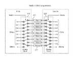
- FIG. 4Ais a block diagram of a host device and a memory device including an IF chip and a core chip in accordance with an embodiment of the present disclosure.
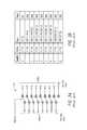
- FIG. 4Bis a truth table of mode register setting and enable inputs of the IF chip and the core chip of FIG. 4A , in accordance with an embodiment of the present disclosure.
- FIG. 4Cis a truth table of mode register setting and enable inputs of the IF chip and the core chip of FIG. 4A , in accordance with an embodiment of the present disclosure.
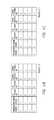
- FIG. 4Dis a schematic diagram of data bus coupling in a domino circuit in a memory chip in accordance with an embodiment of the present disclosure.
- FIG. 4Eis a truth table of data bus coupling in the domino circuit in accordance with an embodiment of the present disclosure.
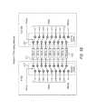
- FIGS. 5A to 5Iare schematic diagrams of data bus coupling between an IF domino circuit and a core domino circuit in a memory chip in accordance with an embodiment of the present disclosure.
- FIG. 4Ais a block diagram of a host device 2 and a memory device 1 including an IF chip 11 and a core chip 12 in accordance with an embodiment of the present disclosure.
- the memory device 1may include the IF chip 11 and a core chip 12 that are stacked with each other. In some embodiments, one or more other core chips may further be stacked with one another over the core chip 12 .
- the host device 2 and the memory device 1may communicate DBI data which has been converted (e.g., encoded, decoded, etc.) using a DBI algorithm.
- the host device 2may include a host DBI encoder 21 .
- the host DBI encoder 21may receive current data bits (Dcur) after receiving previous data bits (Dpre) at a data input node (Di).
- the host DBI encoder 21may encode Dcur with the DBI encoding, when a number of bits that transition in a voltage or logic level (e.g., from a logic high level to a logic low level, or the logic low level to the logic high level) from Dpre to Dcur is more than a half of the number of the data bits in Dcur.
- the host DBI encoder 21may provide Dcur without inversion to an output buffer 211 coupled to data nodes 261 from a data output node (Do) and may further provide a DBI bit “ 0 ” indicative of “no DBI encoding” to an output buffer 212 coupled to a DBI node 262 from a DBI output node (DBIo), if the number of the data bits which transition from Dpre to Dcur is fewer than a half of the number of the data bits to be transmitted.
- Dodata output node
- DBIoDBI output node
- the host DBI encoder 21may provide data Dcur which are inverted to the output buffer 211 coupled to the data nodes 261 and may further provide the DBI bit “ 1 ” indicative of “DBI encoding” to the output buffer 212 coupled to the DBI node 262 , if the number of the data bits which transition from Dpre to Dcur is equal to or more than a half of the number of the data bits to be transmitted.
- the IF chip 11 in the memory device 1may include an IF DBI decoder 23 .
- the IF DBI decoder 23may receive the data bits on the data nodes 261 at an input buffer 231 and may further receive the DBI bit on the DBI node 262 at a DBI input buffer 232 .
- the IF DBI decoder 23may include a Di node that receives the data bits from the input buffer 231 and a DBI input node (DBIi) node that receives the DBI bit from the DRI input buffer 232 .
- the IF DBI decoder 23may be activated by IFDecoderEn signal received at an enable (EN) input of the IF DBI decoder 23 .
- the IF DBI decoder 23determines that the data bits are not subject to DBI-encoding and provides the data bits from a Do node to a TSV data bus 27 coupled to the core chip 12 via an output buffer 234 , if the IFDecoderEn signal is inactive (e.g., the logic low level). The IF DBI decoder 23 determines that data is subject to DBI-encoding, if the IFDecoderEn signal is active (e.g., the logic high level). The IF DBI decoder 23 may further examine if the DBI bit received at the DBIi node is active while the IFDecoderEn signal is active.
- the IF DBI decoder 23may decode the data bits at the Di node and provide the decoded data bits to the Do node. If the DBI bit is inactive (e.g., “0”), the IF DBI decoder 23 may provide the data bits at the Di node to the Do node without data inversion
- the IF chip 11 in the memory device 1may include a DRI encoder 24 .
- the IF DBI encoder 24may include a Di node that receives data bits.
- the IF DBI encoder 24may be activated by IFEncoderEn signal received at an enable (EN) input of the IF DBI encoder 24 .
- the IF DBI encoder 24determines that the current data bits are not subject to DBI-encoding and provides the current data bits from a Do node to the data nodes 261 coupled to the host device 2 . via an output buffer 241 , if the IFEncoderEn signal is inactive (e.g., the logic low level).
- the IF DBI encoder 24determines that the current data bits are subject to DBI-encoding, if the IFEncoderEn signal is active (e.g., the logic high level). For example, the IF DBI encoder 24 may provide the current data bits (e.g., without inversion) from the Do node to the output buffer 241 coupled to the data nodes 261 and may further provide a DBI bit “ 0 ” indicative of “no DBI encoding” from a DBI output node (DBIo) via a multiplexer 243 to an output buffer 242 coupled to the DBI node 262 , if the number of the data bits which transition from previous data bits read from the array 25 to the current data bits is fewer than a half of the number of the data bits to be transmitted.
- DBIoDBI output node
- the IF DBI encoder 24may provide data bits which are the current data bits after inversion to the output buffer 241 coupled to the data nodes 261 and further provide the DBI bit “ 1 ” indicative of “DM encoding” via the multiplexer 243 to the output buffer 242 coupled to the DBI node 262 , if the number of the data bits which transition from the previous data bits to the current data bits is equal to or more than a half of the number of the data bits to be transmitted.
- the multiplexer 243may select the DBIo of the encoder 24 when the IFEncoderEn signal is active (e.g., the logic high level).
- the multiplexer 243may select the output of a DBI input buffer 244 coupled to a DBIchip node of an IF domino circuit 210 that will be described later.
- the host device 2may include a host DBI decoder 22 .
- the host DBI decoder 22may receive the data bits from the data nodes 261 via an input buffer 221 at a data input node (Di) and the DBI bit from the DBI node 262 via an input buffer 222 at a DBI input node (DBIi).
- the IF chip 11 and the core chip 12may include the IF domino circuit 210 and a core domino circuit 220 , respectively.
- the IF domino circuit 210may be located between the output node of the output buffer 234 (or the input node of the DM input buffer 244 ) and a set of TSV data nodes 271 .
- the IF domino circuit 210may further include a Dred node coupled to a redundant TSV node 272 .
- the core domino circuit 220may be located between an input node of an input buffer 281 (or an output node of an output buffer 291 ) and the set of TSV data node 271 .
- the core domino circuit 220may further include a Died node coupled to the redundant TSV node 272 . Description of components corresponding to the domino circuit 130 in FIGS. 3A and 3B will not be repeated.
- the core chip 12may include a core DBI encoder 29 and a core DBI decoder 28 , and the DBI bit may be transmitted to the core chip 12 through the redundant TSV 272 .
- the core DBI decoder 28may perform the same operations as the IF DBI decoder circuit 23 responsive to a COREDecoderEn signal.
- the core DBI encoder 29may perform the same operations as the IF DM encoder circuit 24 responsive to a COREEncoderEn signal.
- FIG. 4Dis a schematic diagram of data bus coupling in a domino circuit in a memory chip in accordance with an embodiment of the present disclosure.
- FIG. 4Eis a truth table of data bus coupling in the domino circuit in accordance with an embodiment of the present disclosure.
- the domino circuit 330 shown FIG. 4Dmay be used as the IF domino circuit 210 and the core domino circuit 220 of FIG. 4A .
- the domino circuit 330may include chip data ports Dchip [ 0 :(x- 1 )] (x: a number of bits of data) coupled to a data node in a chip and TSV data ports Dtsv[ 0 :x] and/or a data redundancy port Dred.
- the domino circuit 330may further include a DBIchip port that may be coupled to the data redundancy port Dred.
- a via coupled to a TSV data port [k](k: a positive integer smaller than (x- 1 )) is defective and the redundancy enable signal RedEN is greater than “0”
- a defective viamay be decoupled (kept in a high-impedance state HiZ) from data transmission paths while the bit data to be transmitted on the defective via may be detoured.
- DBI encoding and decodingmay be executed in the IF chip 11 , responsive to the redundancy enable signal RedEN being greater than “0”.
- the redundancy enable signal RedENis equal to “0” indicating that there is no redundancy bit usage due to a defective via.
- All the chip data ports Dchip[ 7 : 0 ]may be coupled to all the TSV data ports Dtsv[ 7 : 0 ] and the DBI bit may be transmitted to the data redundancy port Dred and DBI encoding and decoding may be executed in the core chip 12 .
- the IF DBI decoder 23may be activated by IFDecoderEn signal received at an enable (EN) input of the IF DBI decoder 23 from a selector 41 a.
- the selector 41 amay receive the RedEn signal and a signal from a mode register 20 a and may provide the IFDecoderEn signal responsive to the RedEn signal and the signal from the mode register 20 a.
- FIG. 4Bis a truth table of mode register setting and enable inputs of the IF chip 11 and the core chip 12 of FIG.
- the selector 41 amay provide the IFDecoderEn and IFEncoderEn signals in an inactive state (e.g., “0”) responsive to the RedEn signal being indicative of no defective via on the TSV data node 271 .
- TSV data nodes 271may be used for transmitting DBI-encoded data, and a redundant TSV node 272 may transmit the DBI bit from the data redundancy port Dred of the IF domino circuit 210 to the data redundancy port Dred of the core domino circuit 220 .
- the selector 41 amay provide the IFDecoderEn and IFEncoderEn signals with the signal of the mode register 20 a as shown in FIG. 4C .
- the IF DBI decoder 23may decode the DBI-encoded data from the input buffer 231 responsive to the DBI bit received from the DBI input buffer 232 , if the IFDecoderEn signal is in the active state.
- the IF DBI decoder 23may provide the data after decoding the DBI-encoding to the output buffer 234 that may be transmitted to the core chip 12 through the IF domino circuit 210 and the TSV data nodes 271 (except the defective via) and the redundant TSV node 272 (in place of the defective via), and the DBI bit may not be transmitted to the core chip 12 via the redundant TSV node 272 .
- a selector 41 bmay receive the RedEn signal and a signal from a mode register 20 b and may provide the COREDecoderEn signal responsive to the RedEn signal and the signal from the mode register 20 b.
- the selector 41 bmay provide the COREDecoderEn signal in an active state (e.g., “1”) responsive to the write DBI enable bit (MR-WDBI enable) in an active state (e.g., “1”) while the RedEn signal is indicative of no defective via on the TSV data node 271 , as shown in FIG. 4B .
- the input buffer 281may receive the data from the Dchip ports of the core domino circuit 220 , when the TSV data ports Dtsv of the core domino circuit 220 receives the data from the TSV data node 271 and the DBI input buffer 282 may receive the DBI bit from the DBIchip port of the core domino circuit 220 , when the data redundancy port Dred of the core domino circuit 220 receives the DBI bit from the redundant TSV node 272 .
- the core DBI decoder 28may be activated by COREDecoderEn signal received at an enable (EN) input of the core DBI decoder 28 from the selector 41 b.
- the core DBI decoder 28may decode the DBI-encoded data from the input buffer 281 responsive to the DBI bit received from the DBI input buffer 282 , if the signal of the mode register 20 b is in the active state.
- the core DBI decoder 28may provide the data after decoding the DBI-encoding to the memory array 25 .
- the selector 41 bmay provide the COREDecoderEn signal in an inactive state (e.g., “0”) as shown in FIG. 4C , responsive to the RedEn signal being equal to or greater than “1”, indicative of the location of the defective via on the TSV data node 271 , and the core DBI decoder 28 and core DBI encoder 29 may be deactivated.
- the TSV data ports Dtsv and the redundant port Dred of the core domino circuit 220may receive the data from the IF domino circuit 210 through the TSV data nodes 271 and the redundant TSV node 272 with detouring the defective via.
- the core domino circuit 220may provide the data to the input buffer 281 and the DBI input buffer 282 from the Dchip and DBIchip ports, respectively.
- the core DBI decoder 28may execute no DBI-decoding operation on the received data and may provide the received data to the array 25 as it is.
- datamay be read from the array 25 and provided to a core DBI encoder 29 in the core chip 12 .
- the core DBI encoder 29may be activated by COREEncoderEn signal received at an enable (EN) input of the core DBI encoder 29 from the selector 41 b.
- the selector 41 bmay receive the RedEn signal and the signal from the mode register 20 b and may provide the COREEncoderEn signal responsive to the RedEn signal and the signal from the mode register 20 b.
- the selector 41 bmay provide the COREEncoderEn signal in an active state (e.g., “1”) responsive to the read DBI enable bit (MR-RDBI enable) in an active state (e.g., “1”) while the RedEn signal is being “0”, indicative of no defective via on the TSV data node 271 , as shown in FIG. 4B .
- an active statee.g., “1”
- MR-RDBI enableread DBI enable bit
- the TSV data node 271may be used for transmitting DBI-encoded data from the TSV data ports Dtsv of the core domino circuit 220 to the TSV data ports Dtsv of the IF domino circuit 210 , and a redundant TSV node 272 may transmit the DBI bit from the data redundancy port Dred of the core domino circuit 220 to the data redundancy port Dred of the IF domino circuit 210 .
- the selector 41 bmay provide the COREEncoderEn signal in an inactive state (e.g., “0”) as shown in FIG. 4C , responsive to the RedEn signal being equal to or greater than “1”, indicative of a location of the defective via on the TSV data node 271 .
- the core DBI encoder 29may encode the data from the array 25 with the DBI algorithm responsive to the active COREEncoderEn signal and may provide the data to the output buffer 291 and an active DBI bit to a DBI output buffer 292 , respectively. If the COREEncoderEn signal in an inactive state (e.g., “0”), the core DBI encoder 29 may not apply DBI encoding and the data is provided to the core domino circuit 220 via the output buffer 291 .
- the core domino circuit 220may receive the data and the DBI bit at the Dchip ports and the DBI chip port from the output buffer 291 and the DBI output buffer 292 , respectively.
- the core domino circuit 220may transmit the data and the DBI bit to the IF chip 11 through the TSV data node 271 and the redundant TSV node 272 from the TSV data ports Dtsv and the data redundancy port Dred, respectively, if the RedEn signal is equal to “0” indicative of no defective via on the TSV data node 271 .
- the TSV data ports Dtsv and the redundant port Dred of the core domino circuit 220may provide the data from the core domino circuit 220 through the TSV data node 271 and the redundant TSV node 272 with detouring the defective via, if the RedEn signal is equal to or greater than “1”, indicative of the location of the defective via on the TSV data node 271 .
- the IF domino circuit 210may receive the data through the TSV data node 271 and the redundant TSV node 272 at the TSV data ports Dtsv and the data redundancy port Dred with detouring the defective via, if the RedEn signal is equal to or greater than “1”.
- the IF DBI encoder 24may be activated by IFencoderEn signal received at an enable (EN) input of the IF DBI encoder 24 from the selector 41 a.
- the selector 41 amay receive the RedEn signal and the signal from the mode register 20 a and may provide the IFEncoderEn signal responsive to the RedEn signal and the signal from the mode register 20 a.
- the selector 41 amay provide the IFEncoderEn signal in an active state (e.g., “1”) responsive to the read DBI enable bit (MR-RDBI enable) in an active state (e.g., “1”) while the RedEn signal is equal to or greater than “1”, indicative of the defective via on the TSV data node 271 , as shown in FIG. 4C .
- the IF DBI encoder 24may encode the data from the IF domino circuit 210 via an input buffer 245 with the DBI algorithm responsive to the active IFEncoderEn signal and may provide the DM-encoded data to an output buffer 241 and an active DBI bit to a multiplexer 243 , respectively.
- the IF domino circuit 210may receive the data and the DBI bit through the TSV data node 271 and the redundant TSV node 272 at the TSV data ports Dtsv and the data redundancy port Dred, respectively, if the RedEn signal is equal to “0” indicative of no defective via on the TSV data node 271 .
- the IF domino circuit 210may provide the data to an input buffer 245 and the DBI bit to the DBI input buffer 244 .
- the selector 41 amay provide the IFEncoderEn signal in an inactive state (e.g., “0”) responsive to the RedEn signal being “0” as shown in FIG. 4B .
- the IF DBI encoder 24may provide the data from the input buffer 245 as provided from the input buffer 245 to the output buffer 241 responsive to the inactive IFEncoderEn signal.
- the DBI input buffer 244may provide the DBI bit to the multiplexer 243 .
- the multiplexer 243may provide the DBI bit that is from either the IF DBI encoder 24 or the core DBI encoder 29 via the DBI input buffer 244 , responsive to the IFEncoderEn signal.
- the multiplexer 243may provide the DBI bit from the DBI input buffer 244 to a DBI output buffer 242 , if the DBI-encoding is performed in the core DBI encoder 29 and the multiplexer 243 may provide the DBI bit from the IF DBI encoder 24 to the DBI output buffer 242 , if the DBI-encoding is executed in the IF DBI encoder 24 or no DBI-encoding is executed (then the DBI bit may be in an inactive state “0”).
- the core DBI decoder 28 and the core DBI encoder 29may perform DBI-decoding and DBI-encoding responsive to the DBI bit when the redundancy enable signal RedEN is equal to “0” indicative of no defective via in the TSV data node 271 .
- the redundant TSV node 272may transmit the DBI bit and DBI-encoded signals are transmitted on vias the TSV data node 271 to reduce currents on the vias of the TSV data node 271 .
- the IF DBI decoder 23 and the IF DBI encoder 24may perform DBI-decoding and DBI-encoding responsive to the DBI bit when the RedEN signal is greater than “0” indicative of a location of a defective via in the TSV data node and the redundant TSV node 272 may transmit a bit of the data while the defective via is disabled.
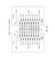
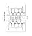
- FIGS. 5A to 5Iare schematic diagrams of data bus coupling between an IF domino circuit 510 and a core domino circuit 520 in a memory chip in accordance with an embodiment of the present disclosure.
- the IF domino circuit 510 and the core domino circuit 520may be the IF domino circuit 210 and the core domino circuit 220 in FIG. 4A .
- a number of data bitsare eight and there are chip data ports Dchip[ 0 : 7 ] in the IF domino circuit 510 and the core domino circuit 520 .
- a number of data bitsmay not be limited to eight, and the data bus coupling may be applicable for any plurality of data bits.
- chip data ports Dchip[ 0 : 7 ] in the IF domino circuit 510 and chip data ports Dchip[ 0 : 7 ] in the core domino circuit 520may be coupled by corresponding vias 571 (TSV- 0 to TSV- 7 ), respectively.
- a DBIchip port of the IF domino circuit 510 and a DBIchip port of the core domino circuit 520may be coupled by a redundancy via 572 (TSV-red).
- the vias 571may include a defective via TSV- 0 .
- the IF domino circuit 510may couple a chip data port Dchip[ 0 ] to the redundancy via 572 (TSV-red) responsive to the RedEn signal equal to “1”.
- the core domino circuit 520may couple a chip data port Dchip[ 0 ] to the redundancy via 572 (TSV-red) responsive to the RedEn signal equal to “1” indicative of the TSV- 0 being defective.
- TSV-redredundancy via 572
- the vias 571may include a defective via TSV- 1 .
- the IF domino circuit 510may couple chip data ports Dchip[ 0 : 1 ] to the redundancy via 572 (TSV-red) and the via 571 (TSV- 0 ) responsive to the RedEn signal equal to “2” indicative of the TSV- 1 being defective.
- the core domino circuit 520may couple chip data ports Dchip[ 0 : 1 ] to the redundancy via 572 (TSV-red) and the via 571 (TSV- 0 ) responsive to the RedEn signal equal to “2”.
- the Dchip[ 0 : 1 ] ports of the IF domino circuit 510 and the core Domino circuit 520may be coupled by the redundancy via 572 (TSV-red) and the via 571 (TSV- 0 ).
- the vias 571may include a defective via TSV- 2 .
- the IF domino circuit 510may couple chip data ports Dchip[ 0 : 2 ] to the redundancy via 572 (TSV-red) and the vias 571 (TSV- 0 and TSV- 1 ) responsive to the RedEn signal equal to “3” indicative of the TSV- 2 being defective.
- the core domino circuit 520may couple chip data ports Dchip[ 0 : 2 ] to the redundancy via 572 (TSV-red) and the vias 571 (TSV- 0 and TSV- 1 ) responsive to the RedEn signal equal to “3”.
- the Dchip[ 0 : 2 ] ports of the IF domino circuit 510 and the core Domino circuit 520may be coupled by the redundancy via 572 (TSV-red) and the vias 571 (TSV- 0 and TSV- 1 ).
- the vias 571may include a detective via TSV- 3 .
- the IF domino circuit 510may couple chip data ports Dchip[ 0 : 3 ] to the redundancy via 572 (NV-red) and the vias 571 (TSV- 0 to TSV- 2 ) responsive to the RedEn signal equal to “4” indicative of the TSV- 3 being defective.
- the core domino circuit 520may couple chip data ports Dchip[ 0 : 3 ] to the redundancy via 572 (TSV-red) and the vias 571 (TSV- 0 to TSV- 2 ) responsive to the RedEn signal equal to “4”.
- the Dchip[ 0 : 1 ] ports of the IF domino circuit 510 and the core Domino circuit 520may be coupled by the redundancy via 572 (TSV-red) and the vias 571 (TSV- 0 to TSV- 2 ).
- the vias 571may include a defective via TSV- 4 .
- the IF domino circuit 510may couple chip data ports Dchip[ 0 : 4 ] to the redundancy via 572 (TSV-red) and the vias 571 (TSV- 0 to TSV- 3 ) responsive to the RedEn signal equal to “5” indicative of the TSV- 4 being defective.
- the core domino circuit 520may couple chip data ports Dchip[ 0 : 4 ] to the redundancy via 572 (TSV-red) and the vias 571 (TSV- 0 to TSV- 3 ) responsive to the RedEn signal equal to “5”.
- the Dchip[ 0 : 4 ] ports of the IF domino circuit 510 and the core Domino circuit 520may be coupled by the redundancy via 572 (TSV-red) and the vias 571 (TSV- 0 to TSV- 3 ).
- the vias 571may include a defective via TSV- 5 .
- the IF domino circuit 510may couple chip data ports Dchip[ 0 : 5 ] to the redundancy via 572 (TSV-red) and the vias 571 (TSV- 0 to TSV- 4 ) responsive to the RedEn signal equal to “6” indicative of the TSV- 5 being defective.
- the core domino circuit 520may couple chip data ports Dchip[ 0 : 5 ] to the redundancy via 572 (TSV-red) and the vias 571 (TSV- 0 to TSV- 4 ) responsive to the RedEn signal equal to “6”.
- the Dchip[ 0 : 5 ] ports of the IF domino circuit 510 and the core Domino circuit 520may be coupled by the redundancy via 572 (TSV-red) and the vias 571 (TSV- 0 to TSV- 4 ).
- the vias 571may include a defective via. TSV- 6 .
- the IF domino circuit 510may couple chip data ports Dchip[ 0 : 6 ] to the redundancy via 572 (TSV-red) and the vias 571 (TSV- 0 to TSV- 5 ) responsive to the RedEn signal equal to “7” indicative of the TSV- 6 being defective.
- the core domino circuit 520may couple chip data ports Dchip[ 0 : 6 ] to the redundancy via 572 (TSV-red) and the vias 571 (TSV- 0 to TSV- 5 ) responsive to the RedEn signal equal to “7”.
- the Dchip[ 0 : 6 ] ports of the IF domino circuit 510 and the core Domino circuit 520may be coupled by the redundancy via 572 (TSV-red) and the vias 571 (TSV- 0 to TSV- 5 ).
- the vias 571may include a defective via TSV- 7 .
- the IF domino circuit 510may couple chip data ports Dchip[ 0 : 7 ] to the redundancy via 572 (TSV-red) and the vias 571 (TSV- 0 to TSV- 6 ) responsive to the RedEn signal equal to “8” indicative of the TSV- 7 being defective.
- the core domino circuit 520may couple chip data ports Dchip[ 0 : 7 ] to the redundancy via 572 (TSV-red) and the vias 571 (TSV- 0 to TSV- 6 ) responsive to the RedEn signal equal to “8”.
- the Dchip[ 0 : 7 ] ports of the IF domino circuit 510 and the core Domino circuit 520may be coupled by the redundancy via 572 (TSV-red) and the vias 571 (TSV- 0 to TSV- 6 ).
- the DBI bitmay not be transmitted through the redundancy via 572 (TSV-red) and DBI-encoding and DM-decoding may be performed in the IF die, because the redundancy via 572 (TSV-red) may be used for repairing the defective via in the vias 571 instead.
- Logic levels of signals used in the embodiments described the aboveare merely examples. However, in other embodiments, combinations of the logic levels of signals other than those specifically described in the present disclosure may be used without departing from the scope of the present disclosure.
Landscapes
- Engineering & Computer Science (AREA)
- Theoretical Computer Science (AREA)
- Physics & Mathematics (AREA)
- General Engineering & Computer Science (AREA)
- Computer Hardware Design (AREA)
- General Physics & Mathematics (AREA)
- Mathematical Physics (AREA)
- Databases & Information Systems (AREA)
- Microelectronics & Electronic Packaging (AREA)
- Static Random-Access Memory (AREA)
- Dram (AREA)
- Probability & Statistics with Applications (AREA)
- For Increasing The Reliability Of Semiconductor Memories (AREA)
Abstract
Description
Claims (10)
Priority Applications (6)
| Application Number | Priority Date | Filing Date | Title |
|---|---|---|---|
| US15/468,742US10146719B2 (en) | 2017-03-24 | 2017-03-24 | Semiconductor layered device with data bus |
| KR1020217036464AKR20210137246A (en) | 2017-03-24 | 2018-03-21 | Semiconductor layered device with data bus |
| CN201880019564.6ACN110462736B (en) | 2017-03-24 | 2018-03-21 | Semiconductor hierarchical device with data bus |
| PCT/US2018/023629WO2018175634A1 (en) | 2017-03-24 | 2018-03-21 | Semiconductor layered device with data bus |
| KR1020197030919AKR20190122875A (en) | 2017-03-24 | 2018-03-21 | Semiconductor layered device with data bus |
| US16/150,505US10635623B2 (en) | 2017-03-24 | 2018-10-03 | Semiconductor layered device with data bus |
Applications Claiming Priority (1)
| Application Number | Priority Date | Filing Date | Title |
|---|---|---|---|
| US15/468,742US10146719B2 (en) | 2017-03-24 | 2017-03-24 | Semiconductor layered device with data bus |
Related Child Applications (1)
| Application Number | Title | Priority Date | Filing Date |
|---|---|---|---|
| US16/150,505DivisionUS10635623B2 (en) | 2017-03-24 | 2018-10-03 | Semiconductor layered device with data bus |
Publications (2)
| Publication Number | Publication Date |
|---|---|
| US20180277175A1 US20180277175A1 (en) | 2018-09-27 |
| US10146719B2true US10146719B2 (en) | 2018-12-04 |
Family
ID=63583553
Family Applications (2)
| Application Number | Title | Priority Date | Filing Date |
|---|---|---|---|
| US15/468,742Active2037-05-10US10146719B2 (en) | 2017-03-24 | 2017-03-24 | Semiconductor layered device with data bus |
| US16/150,505ActiveUS10635623B2 (en) | 2017-03-24 | 2018-10-03 | Semiconductor layered device with data bus |
Family Applications After (1)
| Application Number | Title | Priority Date | Filing Date |
|---|---|---|---|
| US16/150,505ActiveUS10635623B2 (en) | 2017-03-24 | 2018-10-03 | Semiconductor layered device with data bus |
Country Status (4)
| Country | Link |
|---|---|
| US (2) | US10146719B2 (en) |
| KR (2) | KR20190122875A (en) |
| CN (1) | CN110462736B (en) |
| WO (1) | WO2018175634A1 (en) |
Cited By (6)
| Publication number | Priority date | Publication date | Assignee | Title |
|---|---|---|---|---|
| US10635623B2 (en) | 2017-03-24 | 2020-04-28 | Micron Technology, Inc. | Semiconductor layered device with data bus |
| US10903191B2 (en)* | 2019-05-02 | 2021-01-26 | SK Hynix Inc. | Semiconductor chip for repairing through electrode |
| US10922262B2 (en) | 2018-05-23 | 2021-02-16 | Micron Technology, Inc. | Semiconductor layered device with data bus inversion |
| US10964702B2 (en) | 2018-10-17 | 2021-03-30 | Micron Technology, Inc. | Semiconductor device with first-in-first-out circuit |
| US20220083435A1 (en)* | 2018-12-29 | 2022-03-17 | Xi'an Uniic Semiconductors Co., Ltd. | Data backup and recovery method for nvdimm, nvdimm controller and nvdimm |
| US20240193114A1 (en)* | 2022-12-12 | 2024-06-13 | Global Unichip Corporation | Dbi encoding device and dbi encoding method |
Families Citing this family (9)
| Publication number | Priority date | Publication date | Assignee | Title |
|---|---|---|---|---|
| US9922686B2 (en) | 2016-05-19 | 2018-03-20 | Micron Technology, Inc. | Apparatuses and methods for performing intra-module databus inversion operations |
| KR20190029227A (en)* | 2017-09-12 | 2019-03-20 | 에스케이하이닉스 주식회사 | Data transmission circuit, semiconductor apparatus and semiconductor system using the same |
| KR102639154B1 (en)* | 2018-04-16 | 2024-02-22 | 에스케이하이닉스 주식회사 | Memory device and operation method of the same |
| US20200183622A1 (en)* | 2018-12-07 | 2020-06-11 | Micron Technology, Inc. | Memory circuit package with adjustable active channel count |
| JP6994649B2 (en)* | 2019-07-09 | 2022-01-14 | パナソニックIpマネジメント株式会社 | Semiconductor memory device, error notification method |
| WO2021087498A1 (en) | 2020-02-05 | 2021-05-06 | Zeku, Inc. | Power saving techniques for bb-rf interface |
| US11705429B2 (en)* | 2020-09-04 | 2023-07-18 | Micron Technology, Inc. | Redundant through-silicon vias |
| US11494126B1 (en)* | 2021-05-07 | 2022-11-08 | Western Digital Technologies, Inc. | Toggle mode (TM) coding with circuit bounded array memory |
| CN115842013B (en)* | 2023-02-13 | 2023-06-09 | 浙江力积存储科技有限公司 | A three-dimensional stack memory and its data processing method |
Citations (55)
| Publication number | Priority date | Publication date | Assignee | Title |
|---|---|---|---|---|
| US4365247A (en)* | 1980-01-11 | 1982-12-21 | Societe Anonyme De Telecommunications | End station digital transmission link relieving system |
| US5331320A (en) | 1991-11-21 | 1994-07-19 | International Business Machines Corporation | Coding method and apparatus using quaternary codes |
| JPH11283396A (en) | 1998-03-27 | 1999-10-15 | Sony Corp | Memory device |
| US6032248A (en) | 1998-04-29 | 2000-02-29 | Atmel Corporation | Microcontroller including a single memory module having a data memory sector and a code memory sector and supporting simultaneous read/write access to both sectors |
| US6115301A (en)* | 1998-03-03 | 2000-09-05 | Kabushiki Kaisha Toshiba | Semiconductor memory device having defect relieving system using data line shift method |
| US6333915B1 (en)* | 1997-07-03 | 2001-12-25 | Nec Corparation | On-line line monitor system |
| US20020156953A1 (en) | 2001-02-28 | 2002-10-24 | Beiley Mark A. | Dynamic bus inversion method |
| US6518893B1 (en) | 2001-08-24 | 2003-02-11 | Xilinx, Inc. | Method and apparatus for multilevel signal operation |
| US6584526B1 (en) | 2000-09-21 | 2003-06-24 | Intel Corporation | Inserting bus inversion scheme in bus path without increased access latency |
| US20030170020A1 (en)* | 1999-12-16 | 2003-09-11 | At&T Corp. | Method and apparatus for capacity-efficient restoration in an optical communication system |
| US6741190B2 (en) | 2001-02-01 | 2004-05-25 | Nec Corporation | Method and apparatus for adaptive bus coding for low power deep sub-micron designs |
| US20040109509A1 (en) | 2002-12-10 | 2004-06-10 | William Stonecypher | Technique for improving the quality of digital signals in a multi-level signaling system |
| US20040135709A1 (en) | 2000-12-27 | 2004-07-15 | Cornelius William P. | Methods and apparatus for constant-weight encoding and decoding |
| US20050288642A1 (en) | 2002-07-25 | 2005-12-29 | Uni-Charm Corporation | Top sheet of hygroscopic article, hygrosocopic article using the top sheet, and selection and evaluation method for top sheet |
| US20050289435A1 (en) | 2004-06-29 | 2005-12-29 | Mulla Dean A | Fast approximate DINV calculation in parallel with coupled ECC generation or correction |
| US20070008008A1 (en) | 2005-07-06 | 2007-01-11 | Hynix Semiconductor Inc. | Data Output Device and Method of Semiconductor Device |
| US20070096950A1 (en) | 2005-10-31 | 2007-05-03 | Seagate Technology Llc | Structured set partitioning and multilevel coding for partial response channels |
| US7280412B2 (en) | 2005-11-21 | 2007-10-09 | Samsung Electronics Co., Ltd. | Circuits and methods for data bus inversion in a semiconductor memory |
| US7405981B2 (en) | 2005-03-11 | 2008-07-29 | Infineon Technologies Ag | Circuit for data bit inversion |
| US7405984B2 (en) | 2006-09-19 | 2008-07-29 | Lsi Corporation | System and method for providing programmable delay read data strobe gating with voltage and temperature compensation |
| US20080225603A1 (en) | 2007-03-15 | 2008-09-18 | Thomas Hein | Circuit |
| US7501963B1 (en) | 2007-10-17 | 2009-03-10 | Micron Technology, Inc. | Balanced data bus inversion |
| US20090182918A1 (en) | 2008-01-16 | 2009-07-16 | Micron Technology, Inc. | Data bus inversion apparatus, systems, and methods |
| US20090190690A1 (en) | 2008-01-30 | 2009-07-30 | Fujitsu Limited | Communication system |
| US20090238300A1 (en) | 2008-03-21 | 2009-09-24 | Micron Technology, Inc. | Multi-level signaling for low power, short channel applications |
| US20090274245A1 (en) | 2008-05-02 | 2009-11-05 | Micron Technology, Inc. | Apparatus and methods having majority bit detection |
| US20090313521A1 (en)* | 2008-06-11 | 2009-12-17 | Micron Technology, Inc. | Data bus inversion usable in a memory system |
| US20100027989A1 (en)* | 2006-06-01 | 2010-02-04 | Polatis Limited | Network Protection Switching Mechanisms and Methods of Network Protection |
| US20100042889A1 (en) | 2008-08-15 | 2010-02-18 | Micron Technology, Inc. | Memory system and method using a memory device die stacked with a logic die using data encoding, and system using the memory system |
| US20100199017A1 (en) | 2009-02-05 | 2010-08-05 | Micron Technology, Inc. | Data Encoding Using Spare Channels in a Memory System |
| US20110018517A1 (en) | 2008-08-04 | 2011-01-27 | Candage Anthony B | Multi-level signaling |
| US20110116786A1 (en)* | 2009-11-13 | 2011-05-19 | Verizon Patent And Licensing Inc. | Hot-swapping in-line optical amplifiers in an optical network |
| US8014196B2 (en) | 2008-08-28 | 2011-09-06 | Agere Systems Inc. | Reduced-power programming of multi-level cell (MLC) memory |
| US20110222623A1 (en)* | 2010-03-10 | 2011-09-15 | Micron Technology, Inc. | Communication Interface With Configurable Encoding Based on Channel Termination |
| US20110252171A1 (en) | 2010-04-12 | 2011-10-13 | Dearth Glenn A | Reducing simultaneous switching outputs using data bus inversion signaling |
| US20120131244A1 (en)* | 2009-07-13 | 2012-05-24 | Rambus Inc. | Encoding Data Using Combined Data Mask and Data Bus Inversion |
| US8207796B2 (en) | 2009-10-20 | 2012-06-26 | Delphi Technologies, Inc. | Stripline termination circuit having resonators |
| US20120195131A1 (en) | 2007-11-29 | 2012-08-02 | George Pax | Memory register encoding apparatus and methods |
| US20120206280A1 (en)* | 2010-01-20 | 2012-08-16 | Rambus Inc. | Multiple Word Data Bus Inversion |
| US20130091327A1 (en) | 2011-09-29 | 2013-04-11 | Elpida Memory, Inc. | Semiconductor device performing burst order control and data bus inversion |
| US20130307708A1 (en) | 2012-05-18 | 2013-11-21 | Micron Technology, Inc. | Methods and apparatuses for low-power multi-level encoded signals |
| US8762813B2 (en) | 2010-05-17 | 2014-06-24 | Skymedi Corporation | Configurable coding system and method of multiple ECCS |
| US20140281075A1 (en)* | 2013-03-15 | 2014-09-18 | Qualcomm Incorporated | Data bus inversion (dbi) encoding based on the speed of operation |
| US20140289440A1 (en) | 2013-03-15 | 2014-09-25 | Gsi Technology, Inc. | Systems and methods involving data bus inversion memory circuitry, configuration and/or operation |
| US20140289460A1 (en) | 2013-03-15 | 2014-09-25 | Gsi Technology, Inc. | Systems and methods involving data bus inversion memory circuitry, configuration and/or operation including data signals grouped into 10 bits and/or other features |
| WO2014151637A1 (en) | 2013-03-15 | 2014-09-25 | Qualcomm Incorporated | Memory interface offset signaling |
| US9025409B2 (en) | 2011-08-05 | 2015-05-05 | Rambus Inc. | Memory buffers and modules supporting dynamic point-to-point connections |
| US9091727B1 (en) | 2012-10-16 | 2015-07-28 | Xilinx, Inc. | Configuration and testing of multiple-die integrated circuits |
| US20150229325A1 (en) | 2014-02-07 | 2015-08-13 | Qualcomm Incorporated | Encoding for partitioned data bus |
| US20150227417A1 (en) | 2014-02-10 | 2015-08-13 | SK Hynix Inc. | Semiconductor memory apparatus and operating method thereof |
| US20150287446A1 (en) | 2014-04-03 | 2015-10-08 | SK Hynix Inc. | Semiconductor memory apparatus and system using the same |
| US20150356047A1 (en) | 2014-06-06 | 2015-12-10 | Micron Technology, Inc. | Apparatuses and methods for performing a databus inversion operation |
| US9268719B2 (en) | 2011-08-05 | 2016-02-23 | Rambus Inc. | Memory signal buffers and modules supporting variable access granularity |
| US20160173128A1 (en)* | 2014-12-10 | 2016-06-16 | Rambus Inc. | Memory controller and method of data bus inversion using an error detection correction code |
| US20170337951A1 (en) | 2016-05-19 | 2017-11-23 | Micron Technology, Inc. | Apparatuses and methods for performing intra-module databus inversion operations |
Family Cites Families (17)
| Publication number | Priority date | Publication date | Assignee | Title |
|---|---|---|---|---|
| US5274593A (en)* | 1990-09-28 | 1993-12-28 | Intergraph Corporation | High speed redundant rows and columns for semiconductor memories |
| JPH04301290A (en) | 1991-03-28 | 1992-10-23 | Nec Corp | Pushup memory circuit |
| JPH11176158A (en) | 1997-12-10 | 1999-07-02 | Fujitsu Ltd | Latch circuit, data output circuit, and semiconductor device having the same |
| US6367027B1 (en) | 1999-03-22 | 2002-04-02 | Infineon Technologies Ag | Skew pointer generation |
| KR100345285B1 (en) | 1999-08-07 | 2002-07-25 | 한국과학기술원 | Digital driving circuit for LCD |
| JP3799197B2 (en)* | 1999-08-26 | 2006-07-19 | 株式会社東芝 | Semiconductor memory device |
| KR100666320B1 (en) | 2000-07-18 | 2007-01-09 | 삼성전자주식회사 | Shift register and driving circuit of liquid crystal display device employing the same |
| US6696854B2 (en) | 2001-09-17 | 2004-02-24 | Broadcom Corporation | Methods and circuitry for implementing first-in first-out structure |
| US7454559B2 (en) | 2006-03-22 | 2008-11-18 | Infineon Technologies Ag | Filtering bit position in a memory |
| US8552891B2 (en) | 2006-05-27 | 2013-10-08 | Samsung Electronics Co., Ltd. | Method and apparatus for parallel data interfacing using combined coding and recording medium therefor |
| CN101042637A (en) | 2007-04-06 | 2007-09-26 | 威盛电子股份有限公司 | FIFO buffer unit and FIFO buffer method |
| US8706958B2 (en)* | 2011-09-01 | 2014-04-22 | Thomas Hein | Data mask encoding in data bit inversion scheme |
| US10001948B2 (en) | 2013-05-13 | 2018-06-19 | Rambus Inc. | Buffer circuit with data bit inversion |
| KR101692857B1 (en) | 2013-11-26 | 2017-01-05 | 한국전자통신연구원 | Digital serial-to-parallel converter and GaAs MMIC using the same |
| KR102357899B1 (en)* | 2014-01-29 | 2022-02-03 | 마벨 아시아 피티이 엘티디. | Method and apparatus for valid encoding |
| US10373657B2 (en) | 2016-08-10 | 2019-08-06 | Micron Technology, Inc. | Semiconductor layered device with data bus |
| US10146719B2 (en) | 2017-03-24 | 2018-12-04 | Micron Technology, Inc. | Semiconductor layered device with data bus |
- 2017
- 2017-03-24USUS15/468,742patent/US10146719B2/enactiveActive
- 2018
- 2018-03-21CNCN201880019564.6Apatent/CN110462736B/enactiveActive
- 2018-03-21KRKR1020197030919Apatent/KR20190122875A/ennot_activeCeased
- 2018-03-21KRKR1020217036464Apatent/KR20210137246A/ennot_activeAbandoned
- 2018-03-21WOPCT/US2018/023629patent/WO2018175634A1/ennot_activeCeased
- 2018-10-03USUS16/150,505patent/US10635623B2/enactiveActive
Patent Citations (81)
| Publication number | Priority date | Publication date | Assignee | Title |
|---|---|---|---|---|
| US4365247A (en)* | 1980-01-11 | 1982-12-21 | Societe Anonyme De Telecommunications | End station digital transmission link relieving system |
| US5331320A (en) | 1991-11-21 | 1994-07-19 | International Business Machines Corporation | Coding method and apparatus using quaternary codes |
| US6333915B1 (en)* | 1997-07-03 | 2001-12-25 | Nec Corparation | On-line line monitor system |
| US6115301A (en)* | 1998-03-03 | 2000-09-05 | Kabushiki Kaisha Toshiba | Semiconductor memory device having defect relieving system using data line shift method |
| JPH11283396A (en) | 1998-03-27 | 1999-10-15 | Sony Corp | Memory device |
| US6032248A (en) | 1998-04-29 | 2000-02-29 | Atmel Corporation | Microcontroller including a single memory module having a data memory sector and a code memory sector and supporting simultaneous read/write access to both sectors |
| US20030170020A1 (en)* | 1999-12-16 | 2003-09-11 | At&T Corp. | Method and apparatus for capacity-efficient restoration in an optical communication system |
| US6584526B1 (en) | 2000-09-21 | 2003-06-24 | Intel Corporation | Inserting bus inversion scheme in bus path without increased access latency |
| US20040135709A1 (en) | 2000-12-27 | 2004-07-15 | Cornelius William P. | Methods and apparatus for constant-weight encoding and decoding |
| US6844833B2 (en) | 2000-12-27 | 2005-01-18 | Apple Computer, Inc. | Methods and apparatus for constant-weight encoding and decoding |
| US6741190B2 (en) | 2001-02-01 | 2004-05-25 | Nec Corporation | Method and apparatus for adaptive bus coding for low power deep sub-micron designs |
| US20020156953A1 (en) | 2001-02-28 | 2002-10-24 | Beiley Mark A. | Dynamic bus inversion method |
| US6518893B1 (en) | 2001-08-24 | 2003-02-11 | Xilinx, Inc. | Method and apparatus for multilevel signal operation |
| US20050288642A1 (en) | 2002-07-25 | 2005-12-29 | Uni-Charm Corporation | Top sheet of hygroscopic article, hygrosocopic article using the top sheet, and selection and evaluation method for top sheet |
| US20040109509A1 (en) | 2002-12-10 | 2004-06-10 | William Stonecypher | Technique for improving the quality of digital signals in a multi-level signaling system |
| US7113550B2 (en) | 2002-12-10 | 2006-09-26 | Rambus Inc. | Technique for improving the quality of digital signals in a multi-level signaling system |
| US20050289435A1 (en) | 2004-06-29 | 2005-12-29 | Mulla Dean A | Fast approximate DINV calculation in parallel with coupled ECC generation or correction |
| US7405981B2 (en) | 2005-03-11 | 2008-07-29 | Infineon Technologies Ag | Circuit for data bit inversion |
| US20070008008A1 (en) | 2005-07-06 | 2007-01-11 | Hynix Semiconductor Inc. | Data Output Device and Method of Semiconductor Device |
| US20070096950A1 (en) | 2005-10-31 | 2007-05-03 | Seagate Technology Llc | Structured set partitioning and multilevel coding for partial response channels |
| US7280412B2 (en) | 2005-11-21 | 2007-10-09 | Samsung Electronics Co., Ltd. | Circuits and methods for data bus inversion in a semiconductor memory |
| US20080019451A1 (en) | 2005-11-21 | 2008-01-24 | Seong-Jin Jang | Circuits and methods for data bus inversion in a semiconductor memory |
| US20100027989A1 (en)* | 2006-06-01 | 2010-02-04 | Polatis Limited | Network Protection Switching Mechanisms and Methods of Network Protection |
| US7405984B2 (en) | 2006-09-19 | 2008-07-29 | Lsi Corporation | System and method for providing programmable delay read data strobe gating with voltage and temperature compensation |
| US20080225603A1 (en) | 2007-03-15 | 2008-09-18 | Thomas Hein | Circuit |
| US8207976B2 (en) | 2007-03-15 | 2012-06-26 | Qimonda Ag | Circuit |
| US7501963B1 (en) | 2007-10-17 | 2009-03-10 | Micron Technology, Inc. | Balanced data bus inversion |
| US20090179782A1 (en) | 2007-10-17 | 2009-07-16 | Micron Technology, Inc. | Balanced Data Bus Inversion |
| US7701368B2 (en) | 2007-10-17 | 2010-04-20 | Round Rock Research, Llc | Balanced data bus inversion |
| US8018358B2 (en) | 2007-10-17 | 2011-09-13 | Round Rock Research, Llc | Balanced data bus inversion |
| US20120195131A1 (en) | 2007-11-29 | 2012-08-02 | George Pax | Memory register encoding apparatus and methods |
| US9048856B2 (en) | 2008-01-16 | 2015-06-02 | Micron Technology, Inc. | Data bus inversion apparatus, systems, and methods |
| US8094045B2 (en) | 2008-01-16 | 2012-01-10 | Micron Technology, Inc. | Data bus inversion apparatus, systems, and methods |
| US7616133B2 (en) | 2008-01-16 | 2009-11-10 | Micron Technology, Inc. | Data bus inversion apparatus, systems, and methods |
| US8766828B2 (en) | 2008-01-16 | 2014-07-01 | Micron Technology, Inc. | Data bus inversion apparatus, systems, and methods |
| US20100026533A1 (en) | 2008-01-16 | 2010-02-04 | Micron Technology, Inc. | Data Bus Inversion Apparatus, Systems, and Methods |
| US20090182918A1 (en) | 2008-01-16 | 2009-07-16 | Micron Technology, Inc. | Data bus inversion apparatus, systems, and methods |
| US20090190690A1 (en) | 2008-01-30 | 2009-07-30 | Fujitsu Limited | Communication system |
| US8026740B2 (en) | 2008-03-21 | 2011-09-27 | Micron Technology, Inc. | Multi-level signaling for low power, short channel applications |
| US20110316726A1 (en) | 2008-03-21 | 2011-12-29 | Micron Technology, Inc. | Low power multi-level signaling |
| US20090238300A1 (en) | 2008-03-21 | 2009-09-24 | Micron Technology, Inc. | Multi-level signaling for low power, short channel applications |
| US20090274245A1 (en) | 2008-05-02 | 2009-11-05 | Micron Technology, Inc. | Apparatus and methods having majority bit detection |
| US9116828B2 (en) | 2008-06-11 | 2015-08-25 | Micron Technology, Inc. | Data bus inversion usable in a memory system |
| US20090313521A1 (en)* | 2008-06-11 | 2009-12-17 | Micron Technology, Inc. | Data bus inversion usable in a memory system |
| US20110018517A1 (en) | 2008-08-04 | 2011-01-27 | Candage Anthony B | Multi-level signaling |
| US8826101B2 (en) | 2008-08-15 | 2014-09-02 | Micron Technology, Inc. | Memory system and method using a memory device die stacked with a logic die using data encoding, and system using the memory system |
| US20100042889A1 (en) | 2008-08-15 | 2010-02-18 | Micron Technology, Inc. | Memory system and method using a memory device die stacked with a logic die using data encoding, and system using the memory system |
| US20140053040A1 (en) | 2008-08-15 | 2014-02-20 | Micron Technology, Inc. | Memory system and method using a memory device die stacked with a logic die using data encoding, and system using the memory system |
| US8014196B2 (en) | 2008-08-28 | 2011-09-06 | Agere Systems Inc. | Reduced-power programming of multi-level cell (MLC) memory |
| US20100199017A1 (en) | 2009-02-05 | 2010-08-05 | Micron Technology, Inc. | Data Encoding Using Spare Channels in a Memory System |
| US20120131244A1 (en)* | 2009-07-13 | 2012-05-24 | Rambus Inc. | Encoding Data Using Combined Data Mask and Data Bus Inversion |
| US8207796B2 (en) | 2009-10-20 | 2012-06-26 | Delphi Technologies, Inc. | Stripline termination circuit having resonators |
| US20110116786A1 (en)* | 2009-11-13 | 2011-05-19 | Verizon Patent And Licensing Inc. | Hot-swapping in-line optical amplifiers in an optical network |
| US20120206280A1 (en)* | 2010-01-20 | 2012-08-16 | Rambus Inc. | Multiple Word Data Bus Inversion |
| US8879654B2 (en) | 2010-03-10 | 2014-11-04 | Micron Technology, Inc. | Communication interface with configurable encoding based on channel termination |
| US20110222623A1 (en)* | 2010-03-10 | 2011-09-15 | Micron Technology, Inc. | Communication Interface With Configurable Encoding Based on Channel Termination |
| US20110252171A1 (en) | 2010-04-12 | 2011-10-13 | Dearth Glenn A | Reducing simultaneous switching outputs using data bus inversion signaling |
| US8762813B2 (en) | 2010-05-17 | 2014-06-24 | Skymedi Corporation | Configurable coding system and method of multiple ECCS |
| US9268719B2 (en) | 2011-08-05 | 2016-02-23 | Rambus Inc. | Memory signal buffers and modules supporting variable access granularity |
| US9025409B2 (en) | 2011-08-05 | 2015-05-05 | Rambus Inc. | Memory buffers and modules supporting dynamic point-to-point connections |
| US20130091327A1 (en) | 2011-09-29 | 2013-04-11 | Elpida Memory, Inc. | Semiconductor device performing burst order control and data bus inversion |
| US20130307708A1 (en) | 2012-05-18 | 2013-11-21 | Micron Technology, Inc. | Methods and apparatuses for low-power multi-level encoded signals |
| US9148170B2 (en) | 2012-05-18 | 2015-09-29 | Micron Technology, Inc. | Methods and apparatuses for low-power multi-level encoded signals |
| US20150022383A1 (en) | 2012-05-18 | 2015-01-22 | Micron Technology, Inc. | Methods and apparatuses for low-power multi-level encoded signals |
| US8854236B2 (en) | 2012-05-18 | 2014-10-07 | Micron Technology, Inc. | Methods and apparatuses for low-power multi-level encoded signals |
| US9091727B1 (en) | 2012-10-16 | 2015-07-28 | Xilinx, Inc. | Configuration and testing of multiple-die integrated circuits |
| US9798693B2 (en)* | 2013-03-15 | 2017-10-24 | Qualcomm Incorporated | Data bus inversion (DBI) encoding based on the speed of operation |
| US20140289460A1 (en) | 2013-03-15 | 2014-09-25 | Gsi Technology, Inc. | Systems and methods involving data bus inversion memory circuitry, configuration and/or operation including data signals grouped into 10 bits and/or other features |
| US20140281075A1 (en)* | 2013-03-15 | 2014-09-18 | Qualcomm Incorporated | Data bus inversion (dbi) encoding based on the speed of operation |
| US20140289440A1 (en) | 2013-03-15 | 2014-09-25 | Gsi Technology, Inc. | Systems and methods involving data bus inversion memory circuitry, configuration and/or operation |
| WO2014151637A1 (en) | 2013-03-15 | 2014-09-25 | Qualcomm Incorporated | Memory interface offset signaling |
| US20150229325A1 (en) | 2014-02-07 | 2015-08-13 | Qualcomm Incorporated | Encoding for partitioned data bus |
| US20150227417A1 (en) | 2014-02-10 | 2015-08-13 | SK Hynix Inc. | Semiconductor memory apparatus and operating method thereof |
| US20150287446A1 (en) | 2014-04-03 | 2015-10-08 | SK Hynix Inc. | Semiconductor memory apparatus and system using the same |
| US20150356047A1 (en) | 2014-06-06 | 2015-12-10 | Micron Technology, Inc. | Apparatuses and methods for performing a databus inversion operation |
| US9405721B2 (en) | 2014-06-06 | 2016-08-02 | Micron Technology, Inc. | Apparatuses and methods for performing a databus inversion operation |
| US20160173128A1 (en)* | 2014-12-10 | 2016-06-16 | Rambus Inc. | Memory controller and method of data bus inversion using an error detection correction code |
| US20170337951A1 (en) | 2016-05-19 | 2017-11-23 | Micron Technology, Inc. | Apparatuses and methods for performing intra-module databus inversion operations |
| WO2017200820A2 (en) | 2016-05-19 | 2017-11-23 | Micron Technology, Inc. | Apparatuses and methods for performing intra-module databus inversion operations |
| US20180005671A1 (en) | 2016-05-19 | 2018-01-04 | Micron Technology, Inc. | Apparatuses and methods for performing intra-module databus inversion operations |
| US9922686B2 (en) | 2016-05-19 | 2018-03-20 | Micron Technology, Inc. | Apparatuses and methods for performing intra-module databus inversion operations |
Non-Patent Citations (10)
| Title |
|---|
| Cheng, et al., ""Memory bus encoding for low power: a tutorial"", Quality Electronic Design, 2001 International Symposium on Mar. 26-28, 2001, Piscataway, NJ, USA, IEEE Mar. 26, 2001, pp. 199-204. |
| Hollis, , "Data Bus Inversion in High-Speed Memory Applications", IEEE Transactions on Circuits and Systems-II Express Briefs vol. 56, No. 4, Apr. 2009. |
| Hollis, , "Data Bus Inversion in High-Speed Memory Applications", IEEE Transactions on Circuits and Systems—II Express Briefs vol. 56, No. 4, Apr. 2009. |
| International Search Report and Written Opinion dated Jul. 9, 2018 for PCT Application No. PCT/US2018/023629, 13 pages. |
| Rokhani, et al., "Low-Power Bus Transform Coding for Multilevel Signals", IEEE Asia Pacific Conference on Circuits and Systems, Dec. 2006, 1272-1275. |
| Shin, Youngsoo et al., "Partial Bus-Invert Coding for Power Optimization of Application-Specific Systems", IEEE Transactions on Very Large Scale Integration (VLSI) Systems, vol. 9, No. 2, Apr. 2001. |
| Stan, et al., "Bus-Invert Coding for Low-Power I/O", IEEE Transactions on Very Large Scale Integration vol. 3, No. 1, Mar. 1995, 49-58. |
| U.S. Appl. No. 15/703,365, entitled "Apparatuses and Methods for Performing Intra-Module Databus Inversion Operations", filed Sep. 13, 2017, pp. all. |
| U.S. Appl. No. 16/163,471, titled "Semiconductor Device With First-In-First-Out Circuit", filed Oct. 17, 2018. |
| Unpublished U.S. Appl. No. 15/233,821, filed Aug. 10, 2016. |
Cited By (9)
| Publication number | Priority date | Publication date | Assignee | Title |
|---|---|---|---|---|
| US10635623B2 (en) | 2017-03-24 | 2020-04-28 | Micron Technology, Inc. | Semiconductor layered device with data bus |
| US10922262B2 (en) | 2018-05-23 | 2021-02-16 | Micron Technology, Inc. | Semiconductor layered device with data bus inversion |
| US10964702B2 (en) | 2018-10-17 | 2021-03-30 | Micron Technology, Inc. | Semiconductor device with first-in-first-out circuit |
| US11805638B2 (en) | 2018-10-17 | 2023-10-31 | Micron Technology, Inc. | Semiconductor device with first-in-first-out circuit |
| US20220083435A1 (en)* | 2018-12-29 | 2022-03-17 | Xi'an Uniic Semiconductors Co., Ltd. | Data backup and recovery method for nvdimm, nvdimm controller and nvdimm |
| US11914484B2 (en)* | 2018-12-29 | 2024-02-27 | Xi'an Uniic Semiconductors Co., Ltd. | Data backup and recovery method for NVDIMM, NVDIMM controller and NVDIMM |
| US10903191B2 (en)* | 2019-05-02 | 2021-01-26 | SK Hynix Inc. | Semiconductor chip for repairing through electrode |
| US20240193114A1 (en)* | 2022-12-12 | 2024-06-13 | Global Unichip Corporation | Dbi encoding device and dbi encoding method |
| US12093202B2 (en)* | 2022-12-12 | 2024-09-17 | Global Unichip Corporation | DBI encoding device and DBI encoding method |
Also Published As
| Publication number | Publication date |
|---|---|
| US20180277175A1 (en) | 2018-09-27 |
| CN110462736B (en) | 2023-04-18 |
| KR20190122875A (en) | 2019-10-30 |
| US20190034370A1 (en) | 2019-01-31 |
| WO2018175634A1 (en) | 2018-09-27 |
| KR20210137246A (en) | 2021-11-17 |
| CN110462736A (en) | 2019-11-15 |
| US10635623B2 (en) | 2020-04-28 |
Similar Documents
| Publication | Publication Date | Title |
|---|---|---|
| US10146719B2 (en) | Semiconductor layered device with data bus | |
| US11120849B2 (en) | Semiconductor layered device with data bus | |
| US10854310B2 (en) | Shared error detection and correction memory | |
| US11829267B2 (en) | Data encoding using spare channels in a memory system | |
| US10468078B2 (en) | Methods and systems for pin-efficient memory controller interface using vector signaling codes for chip-to-chip communication | |
| US10714206B2 (en) | Selectors on interface die for memory device | |
| US8339879B2 (en) | Repair circuit and semiconductor apparatus including the same | |
| US9773569B2 (en) | Stack type semiconductor memory and semiconductor system using the same | |
| US10964702B2 (en) | Semiconductor device with first-in-first-out circuit | |
| US10185652B2 (en) | Stack access control for memory device | |
| US10332829B2 (en) | Stacked semiconductor apparatus and semiconductor system | |
| US9343438B1 (en) | Semiconductor apparatus having multiple channels | |
| WO2014196410A1 (en) | Semiconductor device |
Legal Events
| Date | Code | Title | Description |
|---|---|---|---|
| AS | Assignment | Owner name:MICRON TECHNOLOGY, INC., IDAHO Free format text:ASSIGNMENT OF ASSIGNORS INTEREST;ASSIGNORS:KONDO, CHIKARA;FUNAHASHI, AKINORI;REEL/FRAME:041727/0592 Effective date:20170324 | |
| AS | Assignment | Owner name:MORGAN STANLEY SENIOR FUNDING, INC., MARYLAND Free format text:SUPPLEMENT NO. 4 TO PATENT SECURITY AGREEMENT;ASSIGNOR:MICRON TECHNOLOGY, INC.;REEL/FRAME:042405/0909 Effective date:20170425 | |
| AS | Assignment | Owner name:JPMORGAN CHASE BANK, N.A., AS COLLATERAL AGENT, ILLINOIS Free format text:SECURITY INTEREST;ASSIGNORS:MICRON TECHNOLOGY, INC.;MICRON SEMICONDUCTOR PRODUCTS, INC.;REEL/FRAME:047540/0001 Effective date:20180703 Owner name:JPMORGAN CHASE BANK, N.A., AS COLLATERAL AGENT, IL Free format text:SECURITY INTEREST;ASSIGNORS:MICRON TECHNOLOGY, INC.;MICRON SEMICONDUCTOR PRODUCTS, INC.;REEL/FRAME:047540/0001 Effective date:20180703 | |
| STCF | Information on status: patent grant | Free format text:PATENTED CASE | |
| AS | Assignment | Owner name:MICRON TECHNOLOGY, INC., IDAHO Free format text:RELEASE BY SECURED PARTY;ASSIGNOR:MORGAN STANLEY SENIOR FUNDING, INC., AS COLLATERAL AGENT;REEL/FRAME:050702/0451 Effective date:20190731 | |
| AS | Assignment | Owner name:MICRON TECHNOLOGY, INC., IDAHO Free format text:RELEASE BY SECURED PARTY;ASSIGNOR:JPMORGAN CHASE BANK, N.A., AS COLLATERAL AGENT;REEL/FRAME:051028/0001 Effective date:20190731 Owner name:MICRON SEMICONDUCTOR PRODUCTS, INC., IDAHO Free format text:RELEASE BY SECURED PARTY;ASSIGNOR:JPMORGAN CHASE BANK, N.A., AS COLLATERAL AGENT;REEL/FRAME:051028/0001 Effective date:20190731 | |
| MAFP | Maintenance fee payment | Free format text:PAYMENT OF MAINTENANCE FEE, 4TH YEAR, LARGE ENTITY (ORIGINAL EVENT CODE: M1551); ENTITY STATUS OF PATENT OWNER: LARGE ENTITY Year of fee payment:4 |