US10146382B2 - Touchscreen electrode arrangement - Google Patents
Touchscreen electrode arrangementDownload PDFInfo
- Publication number
- US10146382B2 US10146382B2US15/185,659US201615185659AUS10146382B2US 10146382 B2US10146382 B2US 10146382B2US 201615185659 AUS201615185659 AUS 201615185659AUS 10146382 B2US10146382 B2US 10146382B2
- Authority
- US
- United States
- Prior art keywords
- electrodes
- touchscreen
- assembly
- array
- active area
- Prior art date
- Legal status (The legal status is an assumption and is not a legal conclusion. Google has not performed a legal analysis and makes no representation as to the accuracy of the status listed.)
- Active, expires
Links
Images


Classifications
- G—PHYSICS
- G06—COMPUTING OR CALCULATING; COUNTING
- G06F—ELECTRIC DIGITAL DATA PROCESSING
- G06F3/00—Input arrangements for transferring data to be processed into a form capable of being handled by the computer; Output arrangements for transferring data from processing unit to output unit, e.g. interface arrangements
- G06F3/01—Input arrangements or combined input and output arrangements for interaction between user and computer
- G06F3/03—Arrangements for converting the position or the displacement of a member into a coded form
- G06F3/041—Digitisers, e.g. for touch screens or touch pads, characterised by the transducing means
- G06F3/044—Digitisers, e.g. for touch screens or touch pads, characterised by the transducing means by capacitive means
- G06F3/0446—Digitisers, e.g. for touch screens or touch pads, characterised by the transducing means by capacitive means using a grid-like structure of electrodes in at least two directions, e.g. using row and column electrodes
- G—PHYSICS
- G06—COMPUTING OR CALCULATING; COUNTING
- G06F—ELECTRIC DIGITAL DATA PROCESSING
- G06F3/00—Input arrangements for transferring data to be processed into a form capable of being handled by the computer; Output arrangements for transferring data from processing unit to output unit, e.g. interface arrangements
- G06F3/01—Input arrangements or combined input and output arrangements for interaction between user and computer
- G06F3/03—Arrangements for converting the position or the displacement of a member into a coded form
- G06F3/041—Digitisers, e.g. for touch screens or touch pads, characterised by the transducing means
- G06F3/044—Digitisers, e.g. for touch screens or touch pads, characterised by the transducing means by capacitive means
- G—PHYSICS
- G06—COMPUTING OR CALCULATING; COUNTING
- G06F—ELECTRIC DIGITAL DATA PROCESSING
- G06F3/00—Input arrangements for transferring data to be processed into a form capable of being handled by the computer; Output arrangements for transferring data from processing unit to output unit, e.g. interface arrangements
- G06F3/01—Input arrangements or combined input and output arrangements for interaction between user and computer
- G06F3/03—Arrangements for converting the position or the displacement of a member into a coded form
- G06F3/041—Digitisers, e.g. for touch screens or touch pads, characterised by the transducing means
- G06F3/0416—Control or interface arrangements specially adapted for digitisers
- G—PHYSICS
- G06—COMPUTING OR CALCULATING; COUNTING
- G06F—ELECTRIC DIGITAL DATA PROCESSING
- G06F3/00—Input arrangements for transferring data to be processed into a form capable of being handled by the computer; Output arrangements for transferring data from processing unit to output unit, e.g. interface arrangements
- G06F3/01—Input arrangements or combined input and output arrangements for interaction between user and computer
- G06F3/03—Arrangements for converting the position or the displacement of a member into a coded form
- G06F3/041—Digitisers, e.g. for touch screens or touch pads, characterised by the transducing means
- G06F3/044—Digitisers, e.g. for touch screens or touch pads, characterised by the transducing means by capacitive means
- G06F3/0443—Digitisers, e.g. for touch screens or touch pads, characterised by the transducing means by capacitive means using a single layer of sensing electrodes
- G—PHYSICS
- G06—COMPUTING OR CALCULATING; COUNTING
- G06F—ELECTRIC DIGITAL DATA PROCESSING
- G06F3/00—Input arrangements for transferring data to be processed into a form capable of being handled by the computer; Output arrangements for transferring data from processing unit to output unit, e.g. interface arrangements
- G06F3/01—Input arrangements or combined input and output arrangements for interaction between user and computer
- G06F3/03—Arrangements for converting the position or the displacement of a member into a coded form
- G06F3/041—Digitisers, e.g. for touch screens or touch pads, characterised by the transducing means
- G06F3/044—Digitisers, e.g. for touch screens or touch pads, characterised by the transducing means by capacitive means
- G06F3/0445—Digitisers, e.g. for touch screens or touch pads, characterised by the transducing means by capacitive means using two or more layers of sensing electrodes, e.g. using two layers of electrodes separated by a dielectric layer
- G—PHYSICS
- G06—COMPUTING OR CALCULATING; COUNTING
- G06F—ELECTRIC DIGITAL DATA PROCESSING
- G06F2203/00—Indexing scheme relating to G06F3/00 - G06F3/048
- G06F2203/041—Indexing scheme relating to G06F3/041 - G06F3/045
- G06F2203/04103—Manufacturing, i.e. details related to manufacturing processes specially suited for touch sensitive devices
Definitions
- Touchscreen displaysare able to detect a person's touch within the active or display area, such as detecting whether a finger is present pressing a fixed-image touchscreen button or detecting the presence and position of a finger on a larger touchscreen display. Some touchscreens can also detect the presence of elements other than a finger, such as a stylus used to generate a digital signature, select objects, or perform other functions on a touchscreen display.
- Touchscreensare often used as interfaces on electronic devices, appliances, and other such electronic systems because the display behind the touchscreen can be easily adapted to provide instruction to the user and to receive various types of input, thereby providing an intuitive interface that requires very little user training to use effectively.
- Inexpensive and efficient touchscreen technologiesenable incorporation of touchscreens into inexpensive commercial devices, but these inexpensive technologies should also desirably be durable and have relatively high immunity to noise, moisture or dirt, or other unintended operation to ensure reliability and longevity of the touchscreen assembly. These desirable attributes also largely apply to other input devices such as trackpads and pen entry tablets.
- Touchscreenscan therefore provide an effective user interface for cell phones, GPS devices, personal digital assistants (PDAs), computers, ATM machines, and other such devices.
- PDAspersonal digital assistants
- Touchscreensuse various technologies to sense touch from a finger or stylus, such as resistive, capacitive, infrared, and acoustic sensors. Resistive sensors rely on touch to cause two resistive elements overlaying the display to contact one another completing a resistive circuit, while capacitive sensors rely on the capacitance of a finger changing the capacitance detected by an array of elements overlaying the display device. Infrared and acoustic touchscreens similarly rely on a finger or stylus to interrupt infrared or acoustic waves across the screen, indicating the presence and position of a touch.
- Minimizing process steps to produce the touchscreen overlay and minimizing external wiring connectionsfurther reduce the cost of producing such a touchscreen display, and makes interfacing the display with electronic control circuitry more straightforward and reliable. Reducing wiring density and number also reduces the number of pins required on a controller chip used to drive the electrode array, which can result in significant space and cost savings. Additionally, it is desirable to reduce the layer count of the touchscreen assembly to reduce cost, reduce light absorption or other optical effects (in applications where this is important), and to increase production yields.
- Various methodshave been proposed and implemented in prior designs to simplify electrode wiring requirements, but often at the expense of other design compromises such as reduced touch resolution or added complexity or cost in other areas.
- Capacitive and resistive touchscreensoften use transparent conductors such as indium tin oxide (ITO) or transparent conductive polymers to form an array over the display image, so that the display image can be seen through the conductive elements used to sense touch.
- ITOindium tin oxide
- the size, shape, and pattern of circuitryhave an effect on the accuracy of the touchscreen, as well as on the visibility of the circuitry overlaying the display.
- a single layer of most suitable conductive elementsis difficult to see when overlaying a display, multiple layers can be easier to see, and circuitry patterns that align closely with patterns on the display can form visible interference or moiré patterns.
- more complex patterns of touchscreen elementscan require more complex routing of lines connecting the elements to external circuitry used to sense touch, such as external circuitry that drives various touchscreen elements and that detects capacitance between multiple touchscreen elements.
- a touchscreen assemblyincludes an array of pairs of electrode elements distributed across an active area of the touchscreen display assembly, such that the density of elements varies to create a sensing gradient.
- the position of an input on the touchscreencan be determined by the proportion of density of the pairs of elements in the area of the input.
- FIG. 1shows a touchscreen assembly using a resistor network coupling touchscreen elements, consistent with the prior art.
- FIG. 2shows first and second drive electrode arrays having electrode densities that progressively vary in distribution proportion according to an example embodiment.
- FIG. 3illustrates electric fields emanating from electrodes in a self-capacitance touchscreen according to an example embodiment.
- FIG. 4shows a simple mutual capacitance touch sensing system according to an example embodiment.
- FIG. 5shows the simple mutual capacitance touch sensing system of FIG. 4 with a finger present according to an example embodiment.
- FIG. 6illustrates a two-dimensional array of distribution modulated touchscreen electrodes according to an example embodiment.
- FIG. 7illustrates finger interaction with capacitive touchscreen electrodes according to an example embodiment.
- FIG. 8illustrates an example touchscreen electrode sequence of five unique drive electrodes in groupings of five according to an example embodiment.
- FIG. 9illustrates an example touchscreen electrode sequence of four unique drive electrodes in groupings of seven according to an example embodiment.
- FIG. 10illustrates first and second drive electrode arrays having electrode densities that vary in proportion progressively in the vertical direction according to an example embodiment.
- FIG. 11illustrates a three-connection receive electrode configuration for a touchscreen display according to an example embodiment.
- FIG. 12illustrates a touchscreen display assembly comprising drive elements such as in FIG. 10 with receive elements such as in FIG. 11 so that the elements do not overlap in the touchscreen active area according to an example embodiment.
- FIG. 13shows a single layer touchscreen assembly overlaying a LCD display panel according to an example embodiment.
- FIG. 14shows an exploded view of a dual layer touchscreen assembly overlaying a LCD display panel according to an example embodiment.
- FIG. 15shows the assembled dual layer touchscreen assembly of FIG. 14 according to an example embodiment.
- FIG. 16shows a cellular telephone having a touchscreen display according to an example embodiment.
- Touchscreensinclude a wide variety of one-dimensional and two-dimensional geometries as may be used to form a slider, wheel, trackpad, tablet, or touchscreen, whether opaque, translucent or transparent, and can be used with a finger, stylus, pen, or other actuation method or device.
- the word ‘touchscreen’will here be used to include any of the foregoing types of geometries or characteristics.
- Capacitive touchscreensare able to detect a person's touch within an active area, and report to a host device the location of one or more touches with good accuracy and resolution. Some capacitive systems can also detect the presence of objects other than a finger, such as a stylus used to perform various functions.
- Touchscreenscan therefore provide an effective user interface for cell phones, GPS devices, personal digital assistants (PDAs), personal computers and notebooks, ATM machines, and other such devices.
- PDAspersonal digital assistants
- ATM machinesATM machines, and other such devices.
- Touchscreensuse various technologies to sense touch from a finger or stylus, such as resistive, capacitive, infrared, and acoustic sensors. Resistive sensors rely on touch to cause two resistive elements overlaying the display to contact one another completing a resistive circuit, while capacitive sensors rely on the capacitance of a finger changing the capacitance detected by an array of electrode elements overlaying the display device. Infrared and acoustic touchscreens similarly rely on a finger or stylus to interrupt infrared or acoustic waves across the screen, indicating the presence and position of a touch.
- Capacitive and resistive touchscreensoften use transparent conductors such as indium tin oxide (ITO) or transparent conductive polymers to form an array over the display image, so that the display image can be seen through the conductive elements used to sense touch.
- ITOindium tin oxide
- the size, shape, density, and pattern of circuitryhave an effect on the resolution and accuracy of the touchscreen, as well as on the optical characteristics of the electrode elements overlaying the display.
- optical propertiesare not important, for example in trackpads that do not overlay a display.
- FIG. 1shows a typical example of such a single-layer mutual capacitance touchscreen display, consistent with the prior art.
- the capacitance between drive electrodes denoted with an “X” and various receive or sense electrodes designated with a “Y”is monitored, and a change in mutual capacitance between the electrodes indicates the presence and position of an input such as a finger or other object.
- the Y electrodesare driven electrodes and the X electrodes are receive electrodes; the pattern is fully reversible, however throughout this patent the convention of X as drive and Y as receive will be used to simplify discussion.
- Mutual capacitance sensor circuitrymeasures the capacitance between the X electrodes and the Y electrodes, which are covered by a dielectric overlay material that provides a sealed housing.
- the X drive signals X 1 , X 2 , and X 3are here extended to various touchscreen drive elements using a resistor divider network chain of resistors 101 , linking the elements between the X or drive electrodes and resulting in electrical interpolation of signals from the electrodes across the various X elements of the touchscreen.
- the X element just below the X 1 connectionwill receive a much stronger X 1 drive signal than an X 2 drive signal, and the proportion of X 1 and X 2 drive signal strengths that couple with the Y electrodes will indicate the relative vertical position of a finger on the display assembly shown.
- a finger placed in the lower half of the display assembly of FIG. 1will impact capacitive coupling between one of the X electrodes having some proportion of X 2 and X 3 drive signals, where the proportion indicates which X element is nearest the finger.
- the X drive electrodesare driven using different series of pulses in one embodiment, such that a suitable number of pulses create an electric field that capacitively couples to the receiving Y electrode.
- the number of pulses neededis dependent on the geometry of the touchscreen electrodes, the dielectric front panel overlaying the electrodes, and other such performance and design characteristics. If each X drive electrode uses a different series of pulses, or is pulsed at different times, the presence and vertical position of a finger can be determined by observing which X drive signals have their capacitive coupling to the Y elements attenuated, and in what proportion the signals are attenuated.
- the Y elements of FIG. 1are similarly split into three regions and have a tapered geometry, such that a finger's presence on the far left side of the touchscreen will affect capacitive coupling between X electrodes and a Y 1 sense electrode, a touch near the center of the touchscreen will affect capacitive coupling between X electrodes and a Y 2 sense electrode, and a touch near the right side of the touchscreen will affect capacitive coupling between X electrodes and a Y 3 sense electrode.
- Touches somewhere between the center and sides of the touchscreenwill affect capacitive coupling in proportion to the area of the tapered Y electrodes under the finger, making horizontal estimation of the finger's position determinable by evaluating the proportion of Y 1 , Y 2 , and Y 3 capacitive coupling that is disrupted due to the finger's presence.
- the touchscreen of FIG. 1relies on the presence of resistors 101 to interpolate the X drive signals between the various X elements of the touchscreen, requiring not only that various conductive traces be laid down to form the touchscreen, but that the X element conductive traces also be electrically coupled to a network of resistors or resistive material having resistances that are reasonably well controlled as to matching tolerance.
- Thisadds extra steps, and considerable cost and complexity to the production process, additionally it also compromises the performance of the sensing circuit, since the resistors introduce an elevated RC time-constant which requires more time to charge and discharge fully, thereby slowing down the acquisition process and potentially introducing other side effects such as increased noise susceptibility. While this design does in fact reduce wiring count thereby reducing space and some cost aspects, it introduces new problems and increases costs in other aspects.
- One example touchscreen embodimenttherefore uses capacitive touchscreen elements in progressively varying electrode densities or proportions across at least one dimension to provide varying field or sense proportional intensities across the touchscreen display.
- FIG. 2shows in plan view a linear capacitive touch slider 201 , wherein two self-capacitance electrode sets A and B are configured with varying distributions along the long axis to effect a sensing gradient which can be interpreted by suitable capacitance sensing circuitry to report the centroid of finger touch 202 (in outline) along the long axis.
- a and B electrodescan be conveniently organized into subgroups or zones, each zone having a varying ratio of A versus B electrode types.
- the ratiois 5:0 of A:B, i.e., there are five A electrodes in this space versus zero B electrodes.
- the ratiois 4:1, and so on until zone 6 is reached where the ratio is 0:5.
- FIG. 3shows the fields emanating from electrodes A of FIG. 2 in cross section along the area of touch 202 (but with no finger present).
- the electric fields 301propagate outwards from the electrodes 302 in all directions; only field lines propagating into the panel are shown diagrammatically for clarity in FIG. 3 .
- Ctis only approximation, since the above formula does not include effects from fringe fields, human skin thickness and moisture content, human body to sensor return path coupling, and the like. Substantial variability in Ct may be observed over a broad range of parametric conditions, nevertheless the formula nevertheless represents a good first order approximation.
- Sensing circuitry 304has two channels, A and B, to drive the respective electrodes 302 .
- the capacitive sensing circuitry 304can be of any style known or unknown to the art, and is not important in understanding the invention.
- FIG. 4shows the field lines associated with electrodes with mutual capacitive coupling.
- field lines from a driven electrode 401(shown as X) operated by a driver 402 and a receive electrode 403 (shown as Y) coupled to a receiver 404 , the fields penetrating through panel 405 .
- a portion of the emitted field 406escapes into free space or other parts of the panel as shown, however we are here primarily concerned with the part of the field which arcs from the X electrode to the Y electrode.
- FIG. 5shows the electrode configuration and circuit of FIG. 4 where the panel is touched by a finger.
- the finger 501causes field lines 502 normally coupling from drive electrode 503 to receive electrode 504 as shown at 506 to be absorbed by the finger 501 .
- the result of this actionis a very detectable decrease in signal level by receiver 505 .
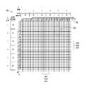
- FIG. 6shows a 2-dimensional sensor array such as a touchscreen, wherein electrodes are arrayed along both the horizontal and vertical axes in a fashion similar to what is shown in FIG. 2 .
- the touchscreen shown at 600can be extended by adding more drive and receive channels, and the size of the panel is not limited to what is shown here.
- Crossovers 601facilitate wiring along the periphery of the active area.
- a touch 602creates signal changes on the XA, XB, YA, and YB electrodes so as to provide sufficient information to signal sensing and processing circuitry to locate the centroid of touch with good accuracy along both axes.
- the electrodes XA and XBoperate identically to YA and YB but are rotated, and use the same circuitry for example of type 304 of FIG. 3 .
- the main sensing area of 600 as shownemploys two sensing layers, one for X and one for Y electrode sets, or, employs a single layer with crossovers at each intersection of an X and a Y electrode.
- the electrode array of FIG. 6can also be operated in mutual capacitance mode, similar to that described in conjunction with FIG. 1 .
- the electrodes along one axisfor example those controlled by XA and XB, are driven to cause fields to be emitted into a panel such as 303 of FIG. 3 .
- the other electrode arrayfor example YA plus YB, receive the electric fields from XA and XB; signals from YA and YB are acquired and processed to provide a location of touch along both the horizontal and vertical axis.
- FIG. 7shows use of intrinsic interpolation to achieve a smooth position response using self-capacitance. It should be understood that mutual capacitance uses similar principles, but the field lines arise from and are affected by slightly different principles.
- electrodes 701emit fields into space through the dielectric panel 702 including to a finger 703 , the changes in strength of which can be modeled as a set of discrete ‘disturbance capacitances’. The value of each disturbance capacitance is dependent on the degree of proximity of the finger 703 to each electrode in accordance with the discussion of FIG. 3 .
- each such capacitance 704can be of any intermediate value, the displacement of touch location can be modeled as an interpolation problem where the point-by-point values are added and a ratio taken between the affected sensing channels.
- the weights of all A and B electrodesare separately summed intrinsically in the sensing process to arrive at two numbers, from which a ratiometric position can be derived. Since all A electrodes are connected together to one sensing channel, and all B electrodes are connected together to a second sensing channel, the detection circuitry has no need to know the individual signal deltas for each A or B sub-electrode in order to determine location of touch.
- the ‘core’ area of touchcomprising the values from 15.8 to 17.2 in the example shown in FIG. 7
- the fringe fields between the electrodes and the finger when an airgap existsare also important in locating touch, as these weaker signals contribute strongly in aggregate to the interpolative process, creating a smooth, non-granular positional response relative to the underlying granularity in electrode frequency and distribution.
- These fringe fieldsexhibit a largely Gaussian rolloff response in two dimensions, i.e., around the perimeter of the finger touch area, and exist in both self and mutual capacitance operating modes.
- the electrodeswill exist as send/receive pairs and the signal levels will drop with increasing object proximity, however the interpolative principles are identical to that of self-capacitance including as to fringe-field effects, varying only in matter of degree.
- the position formula shown at 705is only an example used for illustration and is not the only possible method to calculate position. In a 2D sensor array, the equations used to locate position can become quite sophisticated; the formula for computation is not critical, and discussion of the examples presented here do not limit the scope of the invention or claims.
- FIGS. 4 and 5are important to understanding the operation of the interpolative process described in association with FIG. 7 , if FIG. 7 is operated using electrode pairs in a mutual capacitance mode rather than a self-capacitance mode as drawn. As mentioned previously, in a mutual capacitance implementation the electrodes of FIG. 7 would be replaced with alternating drive and receive electrodes from which the fields would arise.
- FIG. 8shows a group sequence of electrode wiring.
- the wiring sequence illustrated herecan apply equally to self and mutual capacitance.
- FIG. 8also shows that more than two electrode types can be used along each axis, for example in this example there are five channels of sensing, A-E. While FIG. 8 uses five groupings of five channels, other arrangements are possible, for example as shown in FIG. 9 , which shows seven groupings of four channels. Arrangements can include any arbitrary number of elements per group and groups per screen axis, according to the needs of a particular design, however a reasonable group size might typically include at least 3 elements per group. It can also be understood from FIG. 8 , that the plan layout of FIGS. 2 and 6 comprise but one zone of FIG. 8 , for example from zone A 1 to zone B 1 . Extensions in length can therefore be accommodated by means of added sensing channels, for example, channels C through E as shown in FIG. 8 , without limit.
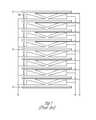
- FIG. 10shows in plan view an electrode layer comprising two channels of mutual or self capacitance, XA and XB, arranged with a vertical split in the middle. Connections for XA and XB exist on the left and right sides, and it should be understood that XA on the left side is the same connection as XA on the right side, and similar for XB. This pattern is similar to FIG. 2 with the exception of the split arrangement as shown at 1003 .
- This electrode layer 1001on its own, can only resolve position along the vertical axis as drawn.
- two drive signals XA and XBdrive two separate but interleaved arrays of horizontal X drive electrodes, as shown generally at 1001 .
- the fingertouches the touchscreen such as at location 1002
- the fingerdesirably interacts with several X drive electrodes, overlaying the XA and XB drive electrodes in proportion to the finger's position on the touchscreen.
- the electrodes coupled to the XA drive signalare in higher proportion near the top of the touchscreen, such that a person who touches the touchscreen in region 1002 intersects with approximately six or seven XA drive electrodes and only one XB drive electrode.
- the relative proportion of XA electrode intersected to XB electrode intersectedsuggests here that the finger is approximately one sixth XB and five sixths XA, or one sixth of the way down from the top of the touchscreen display.
- Fine grain position informationcomes from intrinsic interpolation including from fringe fields as discussed in conjunction with FIG. 7 .
- the electrode spacing and group extent along the vertical axisare typically optimized for smooth performance, for example by making the group extent no more than comparable in dimension to a longitudinal fingerprint chord.
- the vertical extent of the panel 1001can be increased by the use of additional X drive electrodes, for example using an extended and/or enlarged sequence as shown in FIGS. 8 and 9 .
- the drive electrodes of FIG. 10are made of various materials such as indium tin oxide, conductive polymer, metal wire, or fine line metal.
- a more detailed exampleincludes fine line metal electrodes that are approximately 10 micrometers in width or less, and occupy less than 10% of the total screen area, and in a further example less than 5%.
- FIG. 10resolves position only along the vertical axis; the horizontal axis is provided by the plan layout of FIG. 11 , which is interleaved with that of FIG. 10 to compose a single-layer layout shown in FIG. 12 .
- the purpose of gap 1003 of FIG. 10is to allow the spine 1103 of FIG. 11 to fit down the middle as shown in FIG. 12 , to provide for three sensing channels along the horizontal axis.
- three different receive electrodes Y 0 , Y 1 , and Y 2are coupled to the control circuitry, and the three electrodes are coupled to Y elements that are configured in an alternating pattern as shown generally at 1101 such that a the location of a finger touch 1102 covers varying proportions of different Y receive electrodes as it moves from side to side across the touchscreen display.
- a touch in position 1102covering mostly region 4 but also overlapping regions 3 and 5 , covers somewhat more Y 2 element electrodes than Y 1 element electrodes. This indicates that the finger is slightly to the right of the center of region 4 , toward the Y 2 receive element side of the region.
- the Y receive electrodesare therefore able to use interpolation of the finger's impact on capacitive coupling to determine the finger's position with greater accuracy than the five zones laid out in FIG. 11 , much as interpolation or proportional measurements were used in FIG. 10 to determine the finger's position in the vertical axis using X drive electrodes.
- a relatively straightforward array of X drive electrodes as in FIG. 10 and Y receive electrodes as in FIG. 11can therefore be combined to provide a high-performance touchscreen display with very good finger resolution capability along both axes, as is shown in FIG. 12 .
- the composite design of FIG. 12therefore resides in one plane, except for crossovers 1203 on the periphery of the active area.
- the Y electrode layer shown in FIG. 11uses alignment and length-modulation to achieve better interpolation; distribution modulation exists only on layer 10 , as it is difficult to fashion 2-axis distribution modulation in a single layer.
- the design of FIG. 12eliminates the need for resistors 101 of FIG. 1 , yet provides similar resolution and accuracy in a single layer to the design of FIG. 1 , even with one less X channel. Distribution modulation does not suffer from RC time constant problems introduced by the divider resistors of FIG. 1 , thereby allowing for a greater extent of each drive channel than the resistive divider approach, resulting in fewer required drive channels over a given length of screen area.
- the Y receive grid of FIG. 11is laid in between the X drive electrodes of FIG. 10 , such that the X drive electrodes and Y receive electrodes do not overlap in the display region.
- Thisenables formation of the entire electrode set on a substrate using a single process, such as by single pass metal or ITO deposition, resulting in a relatively efficient and inexpensive production process.
- electrodes do not cross within the display regionthere are no regions of the touchscreen display that are more opaque than others, as there are no “stacked” or overlapping electrodes.
- the distribution of electrodes across the touchscreen displayis also generally uniform, resulting in relatively uniform brightness across the touchscreen display.
- a user of touchscreen display 1201places a finger on or near the touchscreen, as shown at 1202 .
- Different series of pulsesare sent via the Xa and Xb drive electrodes, such that the mutual capacitance between the different X drive electrodes and Y conductors can be separately determined, such as by observation of an RC time constant, received pulse amplitude measurement, charge transfer measurement, or another suitable method.
- the presence of a fingerinterrupts the field between the X and Y conductors as in FIG. 5 , a reduction in observed coupling between the drive and receive electrodes is observed.
- the touchscreen display of FIG. 12has several advantages relative to that of FIG. 1 , including the lack of a resistive material coupling the X drive electrodes to interpolate X drive signals between the X drive electrodes. Fewer different materials and process steps are therefore needed to form the touchscreen display of FIG. 12 , and a reduced connection count simplifies connection to external drive and control circuitry.
- FIG. 13shows one physical implementation of a single electrode layer stack over a display such as an LCD.
- the electrodes 1301are printed or otherwise fashioned onto a substrate 1302 , which in some embodiments is a clear plastic sheet such as PET or polycarbonate, or potentially a glass layer.
- Adhesive 1303is used to bond substrate layer 1302 to panel 1304 ; 1303 may be a liquid adhesive, or an adhesive sheet. Assembly may be via a laminating process to provide for an airtight assembly.
- Electrodes 1301may be fashioned from clear ITO, or from ultra fine line metal traces when used with a display. If no display is used, then the optical properties of assembly 1305 are not relevant and any set of suitable materials may be used.
- Gap 1306is an airgap between the display and the assembly 1305 , as is common in the art. In some cases is it advantageous to insert an adhesive layer in this gap and laminate the entire stack to the top of the display.
- FIG. 14shows an assembly stack 1401 which contains two sensing layers, for example as may be used to implement a two-layer version of the design of FIG. 6 .
- Two layers of plastic filmare used, 1402 and 1403 , with respective electrodes 1404 and 1405 fashioned thereon, and assembled with adhesive layers 1406 , 1407 and optionally 1408 via a lamination process to panel 1409 and possibly also to display 1410 .
- FIG. 15shows the layer stack of FIG. 14 as laminated together, but without the adhesive layer 1408 , using instead an airgap 1501 .
- Touchscreensare often used in a variety of applications, from automatic teller machines (ATM machines), home appliances, personal digital assistants and cell phones, and other such devices.
- ATM machinesautomatic teller machines
- FIG. 16One such example cellular telephone or PDA device is illustrated in FIG. 16 .
- the cellular telephone device 1601includes a touchscreen display 1602 comprising a significant portion of the largest surface of the device.
- the large size of the touchscreen 1602enables the touchscreen to present a wide variety of images that can serve along with touchscreen capability to provide input to the device, including a keyboard, a numeric keypad, program or application icons, and various other interfaces as desired.
- the usermay interact with the device by touching with a single finger, such as to select a program for execution or to type a letter on a keyboard displayed on the touchscreen display assembly 1602 , or may use multiple touches such as to zoom in or zoom out when viewing a document or image.
- the displaydoes not change or changes only slightly during device operation, and may recognize only single touches.
- touch sensitive device configurationsare possible and are within the scope of the invention, such as a touchwheel, a linear slider, buttons with reconfigurable displays, and other such configurations.
- Proportionate distribution of drive or receive electrodes coupled to different elements across the touch sensitive devicecan be adapted to any such shape, enabling detection of the region of input on the touchscreen.
- the conductive materialbe either transparent, such as Indium tin oxide or transparent conductive polymer, or be so small as to not significantly interfere with visibility of the display, such as with fine line metal.
- proportional element distribution touchscreen display assembly examples given heregenerally rely on mutual capacitance or self-capacitance to operate, other embodiments of the invention will use other technologies, including other capacitance measures, resistance, or other such sense technologies.
- These example touchscreen assembliesillustrate how a touchscreen can be formed using an array of drive electrodes having a distribution modulation that enables determining an input position by the sensing gradient observed.
- the drive electrodes in a further exampledo not overlap in the active area or field of the touchscreen, eliminating the extra materials, expense, and production steps needed to form resistively-coupled element touchscreens such as that of FIG. 1 .
- image qualityis not degraded, and the relatively uniform electrode density of all electrodes across the touchscreen element avoids causing bright or dark regions in areas of varying electrode density when viewing the display through the touchscreen element.
- Configurations such as the example of FIG. 12provide an efficient system for generating an accurate reading of a finger's location on the touchscreen assembly. These benefits simplify operation of the touchscreen panel, as fewer connections and less filtering and other data processing are needed to ensure reliable touchscreen operation. This in turn leads to lower power consumption in an electronic device incorporating such a touchscreen display assembly, improving power efficiency, increasing battery life, and reducing resource use such as memory and processor consumption.
Landscapes
- Engineering & Computer Science (AREA)
- General Engineering & Computer Science (AREA)
- Theoretical Computer Science (AREA)
- Human Computer Interaction (AREA)
- Physics & Mathematics (AREA)
- General Physics & Mathematics (AREA)
- Position Input By Displaying (AREA)
Abstract
Description
- Ct=the increase in capacitance for one sensing channel due to touch,
- ε=relative permittivity of the panel material,
- A=The intersecting surface area of the electrodes coupled to the sensing channel affected and the finger contact area,
- d=thickness of the dielectric panel
Claims (21)
Priority Applications (1)
| Application Number | Priority Date | Filing Date | Title |
|---|---|---|---|
| US15/185,659US10146382B2 (en) | 2009-10-27 | 2016-06-17 | Touchscreen electrode arrangement |
Applications Claiming Priority (2)
| Application Number | Priority Date | Filing Date | Title |
|---|---|---|---|
| US12/606,934US9372579B2 (en) | 2009-10-27 | 2009-10-27 | Touchscreen electrode arrangement |
| US15/185,659US10146382B2 (en) | 2009-10-27 | 2016-06-17 | Touchscreen electrode arrangement |
Related Parent Applications (1)
| Application Number | Title | Priority Date | Filing Date |
|---|---|---|---|
| US12/606,934ContinuationUS9372579B2 (en) | 2009-10-27 | 2009-10-27 | Touchscreen electrode arrangement |
Publications (2)
| Publication Number | Publication Date |
|---|---|
| US20160299605A1 US20160299605A1 (en) | 2016-10-13 |
| US10146382B2true US10146382B2 (en) | 2018-12-04 |
Family
ID=43897988
Family Applications (2)
| Application Number | Title | Priority Date | Filing Date |
|---|---|---|---|
| US12/606,934Active2034-06-06US9372579B2 (en) | 2009-10-27 | 2009-10-27 | Touchscreen electrode arrangement |
| US15/185,659Active2030-02-24US10146382B2 (en) | 2009-10-27 | 2016-06-17 | Touchscreen electrode arrangement |
Family Applications Before (1)
| Application Number | Title | Priority Date | Filing Date |
|---|---|---|---|
| US12/606,934Active2034-06-06US9372579B2 (en) | 2009-10-27 | 2009-10-27 | Touchscreen electrode arrangement |
Country Status (1)
| Country | Link |
|---|---|
| US (2) | US9372579B2 (en) |
Families Citing this family (58)
| Publication number | Priority date | Publication date | Assignee | Title |
|---|---|---|---|---|
| US9916045B2 (en) | 2009-10-26 | 2018-03-13 | Amtel Corporation | Sense electrode design |
| US9372579B2 (en) | 2009-10-27 | 2016-06-21 | Atmel Corporation | Touchscreen electrode arrangement |
| US8638107B2 (en) | 2009-12-18 | 2014-01-28 | Synaptics Incorporated | Transcapacitive sensor devices with ohmic seams |
| US10268320B2 (en)* | 2010-08-06 | 2019-04-23 | Apple Inc. | Method for disambiguating multiple touches on a projection-scan touch sensor panel |
| US8564314B2 (en) | 2010-11-02 | 2013-10-22 | Atmel Corporation | Capacitive touch sensor for identifying a fingerprint |
| WO2012106424A2 (en)* | 2011-02-02 | 2012-08-09 | 3M Innovative Properties Company | Patterned substrates with darkened mutlilayered conductor traces |
| US8975903B2 (en) | 2011-06-09 | 2015-03-10 | Ford Global Technologies, Llc | Proximity switch having learned sensitivity and method therefor |
| US8928336B2 (en) | 2011-06-09 | 2015-01-06 | Ford Global Technologies, Llc | Proximity switch having sensitivity control and method therefor |
| JP2014515147A (en)* | 2011-06-21 | 2014-06-26 | エンパイア テクノロジー ディベロップメント エルエルシー | Gesture-based user interface for augmented reality |
| US10004286B2 (en) | 2011-08-08 | 2018-06-26 | Ford Global Technologies, Llc | Glove having conductive ink and method of interacting with proximity sensor |
| US9143126B2 (en) | 2011-09-22 | 2015-09-22 | Ford Global Technologies, Llc | Proximity switch having lockout control for controlling movable panel |
| US8994228B2 (en) | 2011-11-03 | 2015-03-31 | Ford Global Technologies, Llc | Proximity switch having wrong touch feedback |
| US10112556B2 (en) | 2011-11-03 | 2018-10-30 | Ford Global Technologies, Llc | Proximity switch having wrong touch adaptive learning and method |
| US8878438B2 (en) | 2011-11-04 | 2014-11-04 | Ford Global Technologies, Llc | Lamp and proximity switch assembly and method |
| US20130127744A1 (en)* | 2011-11-22 | 2013-05-23 | Qualcomm Mems Technologies, Inc. | Wireframe touch sensor design and spatially linearized touch sensor design |
| CN103309522A (en)* | 2012-03-07 | 2013-09-18 | 上海海栎创微电子有限公司 | Real two-point detection algorithm based on self-capacitance technology |
| US9197206B2 (en) | 2012-04-11 | 2015-11-24 | Ford Global Technologies, Llc | Proximity switch having differential contact surface |
| US9944237B2 (en) | 2012-04-11 | 2018-04-17 | Ford Global Technologies, Llc | Proximity switch assembly with signal drift rejection and method |
| US9559688B2 (en) | 2012-04-11 | 2017-01-31 | Ford Global Technologies, Llc | Proximity switch assembly having pliable surface and depression |
| US9065447B2 (en) | 2012-04-11 | 2015-06-23 | Ford Global Technologies, Llc | Proximity switch assembly and method having adaptive time delay |
| US9287864B2 (en) | 2012-04-11 | 2016-03-15 | Ford Global Technologies, Llc | Proximity switch assembly and calibration method therefor |
| US9219472B2 (en) | 2012-04-11 | 2015-12-22 | Ford Global Technologies, Llc | Proximity switch assembly and activation method using rate monitoring |
| US9184745B2 (en) | 2012-04-11 | 2015-11-10 | Ford Global Technologies, Llc | Proximity switch assembly and method of sensing user input based on signal rate of change |
| US9568527B2 (en) | 2012-04-11 | 2017-02-14 | Ford Global Technologies, Llc | Proximity switch assembly and activation method having virtual button mode |
| US9831870B2 (en) | 2012-04-11 | 2017-11-28 | Ford Global Technologies, Llc | Proximity switch assembly and method of tuning same |
| US9520875B2 (en) | 2012-04-11 | 2016-12-13 | Ford Global Technologies, Llc | Pliable proximity switch assembly and activation method |
| US8933708B2 (en) | 2012-04-11 | 2015-01-13 | Ford Global Technologies, Llc | Proximity switch assembly and activation method with exploration mode |
| US9660644B2 (en) | 2012-04-11 | 2017-05-23 | Ford Global Technologies, Llc | Proximity switch assembly and activation method |
| FR2989485B1 (en)* | 2012-04-11 | 2016-02-05 | Commissariat Energie Atomique | TOUCH SENSOR AND METHOD FOR MANUFACTURING SUCH SENSOR |
| US9531379B2 (en) | 2012-04-11 | 2016-12-27 | Ford Global Technologies, Llc | Proximity switch assembly having groove between adjacent proximity sensors |
| US9244572B2 (en)* | 2012-05-04 | 2016-01-26 | Blackberry Limited | Electronic device including touch-sensitive display and method of detecting touches |
| WO2013172829A1 (en)* | 2012-05-16 | 2013-11-21 | Blackberry Limited | Portable electronic device and method of controlling same |
| US9136840B2 (en) | 2012-05-17 | 2015-09-15 | Ford Global Technologies, Llc | Proximity switch assembly having dynamic tuned threshold |
| US8981602B2 (en) | 2012-05-29 | 2015-03-17 | Ford Global Technologies, Llc | Proximity switch assembly having non-switch contact and method |
| US9337832B2 (en) | 2012-06-06 | 2016-05-10 | Ford Global Technologies, Llc | Proximity switch and method of adjusting sensitivity therefor |
| US9641172B2 (en) | 2012-06-27 | 2017-05-02 | Ford Global Technologies, Llc | Proximity switch assembly having varying size electrode fingers |
| US8872764B2 (en) | 2012-06-29 | 2014-10-28 | Qualcomm Mems Technologies, Inc. | Illumination systems incorporating a light guide and a reflective structure and related methods |
| US20140022199A1 (en)* | 2012-07-19 | 2014-01-23 | Texas Instruments Incorporated | Capacitive touch panel having improved response characteristics |
| US9128571B2 (en) | 2012-07-23 | 2015-09-08 | Texas Instruments Incorporated | Capacitive touch panel having improved response characteristics |
| US8922340B2 (en) | 2012-09-11 | 2014-12-30 | Ford Global Technologies, Llc | Proximity switch based door latch release |
| US8796575B2 (en) | 2012-10-31 | 2014-08-05 | Ford Global Technologies, Llc | Proximity switch assembly having ground layer |
| WO2014113983A1 (en) | 2013-01-28 | 2014-07-31 | Texas Instruments Incorporated | Capacitive single layer multi-touch panel having improved response characteristics |
| US9142363B2 (en) | 2013-02-27 | 2015-09-22 | Microchip Technology Germany Gmbh | Method for forming a sensor electrode for a capacitive sensor device |
| US9311204B2 (en) | 2013-03-13 | 2016-04-12 | Ford Global Technologies, Llc | Proximity interface development system having replicator and method |
| US20150226547A1 (en)* | 2014-02-10 | 2015-08-13 | Uni-Pixel Displays, Inc. | Method of aligning transparent substrates using moiré interference |
| JP5852050B2 (en)* | 2013-05-27 | 2016-02-03 | 株式会社ジャパンディスプレイ | Touch detection device, display device with touch detection function, and electronic device |
| US9436324B2 (en) | 2013-11-04 | 2016-09-06 | Blackberry Limited | Electronic device including touch-sensitive display and method of detecting touches |
| US20170024124A1 (en)* | 2014-04-14 | 2017-01-26 | Sharp Kabushiki Kaisha | Input device, and method for controlling input device |
| CN104020908B (en)* | 2014-05-30 | 2017-03-01 | 京东方科技集团股份有限公司 | A kind of driving method of In-cell touch panel, device and display device |
| US10038443B2 (en) | 2014-10-20 | 2018-07-31 | Ford Global Technologies, Llc | Directional proximity switch assembly |
| KR102309163B1 (en)* | 2015-01-07 | 2021-10-06 | 삼성디스플레이 주식회사 | Touch sensor device and display device comprising the same |
| US9654103B2 (en) | 2015-03-18 | 2017-05-16 | Ford Global Technologies, Llc | Proximity switch assembly having haptic feedback and method |
| US10409426B2 (en)* | 2015-04-14 | 2019-09-10 | Ford Global Technologies, Llc | Motion based capacitive sensor system |
| US9548733B2 (en) | 2015-05-20 | 2017-01-17 | Ford Global Technologies, Llc | Proximity sensor assembly having interleaved electrode configuration |
| KR102388590B1 (en)* | 2015-08-13 | 2022-04-21 | 삼성전자주식회사 | Electronic device and method for inputting in electronic device |
| KR102330999B1 (en)* | 2017-08-01 | 2021-11-25 | 삼성전자 주식회사 | Electronic device and method for controlling thereof |
| DE102019209430A1 (en)* | 2019-06-28 | 2020-12-31 | Robert Bosch Gmbh | Sensor device with capacitive sensor |
| CN113179591B (en)* | 2021-04-29 | 2023-05-09 | 深圳市康冠商用科技有限公司 | Capacitive membrane material, manufacturing method thereof and capacitive screen |
Citations (25)
| Publication number | Priority date | Publication date | Assignee | Title |
|---|---|---|---|---|
| US6323846B1 (en) | 1998-01-26 | 2001-11-27 | University Of Delaware | Method and apparatus for integrating manual input |
| US20060032680A1 (en)* | 2004-08-16 | 2006-02-16 | Fingerworks, Inc. | Method of increasing the spatial resolution of touch sensitive devices |
| US20080309635A1 (en) | 2007-06-14 | 2008-12-18 | Epson Imaging Devices Corporation | Capacitive input device |
| US20090315854A1 (en) | 2008-06-18 | 2009-12-24 | Epson Imaging Devices Corporation | Capacitance type input device and display device with input function |
| US7663607B2 (en) | 2004-05-06 | 2010-02-16 | Apple Inc. | Multipoint touchscreen |
| US7864503B2 (en) | 2007-05-11 | 2011-01-04 | Sense Pad Tech Co., Ltd | Capacitive type touch panel |
| US7875814B2 (en) | 2005-07-21 | 2011-01-25 | Tpo Displays Corp. | Electromagnetic digitizer sensor array structure |
| US7920129B2 (en) | 2007-01-03 | 2011-04-05 | Apple Inc. | Double-sided touch-sensitive panel with shield and drive combined layer |
| US20110095997A1 (en) | 2009-10-27 | 2011-04-28 | Qrg Limited | Touchscreen electrode arrangement |
| US20110141051A1 (en)* | 2008-08-14 | 2011-06-16 | Melfas, Inc. | Touch sensing panel including bidirectional adjacent electrodes, and touch sensing apparatus |
| US8031174B2 (en) | 2007-01-03 | 2011-10-04 | Apple Inc. | Multi-touch surface stackup arrangement |
| US8031094B2 (en) | 2009-09-11 | 2011-10-04 | Apple Inc. | Touch controller with improved analog front end |
| US8040326B2 (en) | 2007-06-13 | 2011-10-18 | Apple Inc. | Integrated in-plane switching display and touch sensor |
| US8049732B2 (en) | 2007-01-03 | 2011-11-01 | Apple Inc. | Front-end signal compensation |
| US8179381B2 (en) | 2008-02-28 | 2012-05-15 | 3M Innovative Properties Company | Touch screen sensor |
| US8217902B2 (en) | 2007-04-27 | 2012-07-10 | Tpk Touch Solutions Inc. | Conductor pattern structure of capacitive touch panel |
| US20120243151A1 (en) | 2011-03-21 | 2012-09-27 | Stephen Brian Lynch | Electronic Devices With Convex Displays |
| US20120242592A1 (en) | 2011-03-21 | 2012-09-27 | Rothkopf Fletcher R | Electronic devices with flexible displays |
| WO2012129247A2 (en) | 2011-03-21 | 2012-09-27 | Apple Inc. | Electronic devices with flexible displays |
| US20120243719A1 (en) | 2011-03-21 | 2012-09-27 | Franklin Jeremy C | Display-Based Speaker Structures for Electronic Devices |
| US20120242588A1 (en) | 2011-03-21 | 2012-09-27 | Myers Scott A | Electronic devices with concave displays |
| US20130080755A1 (en) | 2011-09-23 | 2013-03-28 | Wistron Corp. | Method for speeding up the boot time of electric device and electric device using the same |
| US20130076612A1 (en) | 2011-09-26 | 2013-03-28 | Apple Inc. | Electronic device with wrap around display |
| US20130120052A1 (en) | 2011-11-14 | 2013-05-16 | Andrew Siska | Conductive Shield for Shaping an Electric Field of a Conductive Wire |
| US8723824B2 (en) | 2011-09-27 | 2014-05-13 | Apple Inc. | Electronic devices with sidewall displays |
- 2009
- 2009-10-27USUS12/606,934patent/US9372579B2/enactiveActive
- 2016
- 2016-06-17USUS15/185,659patent/US10146382B2/enactiveActive
Patent Citations (26)
| Publication number | Priority date | Publication date | Assignee | Title |
|---|---|---|---|---|
| US6323846B1 (en) | 1998-01-26 | 2001-11-27 | University Of Delaware | Method and apparatus for integrating manual input |
| US7663607B2 (en) | 2004-05-06 | 2010-02-16 | Apple Inc. | Multipoint touchscreen |
| US20060032680A1 (en)* | 2004-08-16 | 2006-02-16 | Fingerworks, Inc. | Method of increasing the spatial resolution of touch sensitive devices |
| US7875814B2 (en) | 2005-07-21 | 2011-01-25 | Tpo Displays Corp. | Electromagnetic digitizer sensor array structure |
| US8031174B2 (en) | 2007-01-03 | 2011-10-04 | Apple Inc. | Multi-touch surface stackup arrangement |
| US8049732B2 (en) | 2007-01-03 | 2011-11-01 | Apple Inc. | Front-end signal compensation |
| US7920129B2 (en) | 2007-01-03 | 2011-04-05 | Apple Inc. | Double-sided touch-sensitive panel with shield and drive combined layer |
| US8217902B2 (en) | 2007-04-27 | 2012-07-10 | Tpk Touch Solutions Inc. | Conductor pattern structure of capacitive touch panel |
| US7864503B2 (en) | 2007-05-11 | 2011-01-04 | Sense Pad Tech Co., Ltd | Capacitive type touch panel |
| US8040326B2 (en) | 2007-06-13 | 2011-10-18 | Apple Inc. | Integrated in-plane switching display and touch sensor |
| US20080309635A1 (en) | 2007-06-14 | 2008-12-18 | Epson Imaging Devices Corporation | Capacitive input device |
| US8179381B2 (en) | 2008-02-28 | 2012-05-15 | 3M Innovative Properties Company | Touch screen sensor |
| US20090315854A1 (en) | 2008-06-18 | 2009-12-24 | Epson Imaging Devices Corporation | Capacitance type input device and display device with input function |
| US20110141051A1 (en)* | 2008-08-14 | 2011-06-16 | Melfas, Inc. | Touch sensing panel including bidirectional adjacent electrodes, and touch sensing apparatus |
| US8031094B2 (en) | 2009-09-11 | 2011-10-04 | Apple Inc. | Touch controller with improved analog front end |
| US20110095997A1 (en) | 2009-10-27 | 2011-04-28 | Qrg Limited | Touchscreen electrode arrangement |
| WO2012129247A2 (en) | 2011-03-21 | 2012-09-27 | Apple Inc. | Electronic devices with flexible displays |
| US20120242592A1 (en) | 2011-03-21 | 2012-09-27 | Rothkopf Fletcher R | Electronic devices with flexible displays |
| US20120243151A1 (en) | 2011-03-21 | 2012-09-27 | Stephen Brian Lynch | Electronic Devices With Convex Displays |
| US20120243719A1 (en) | 2011-03-21 | 2012-09-27 | Franklin Jeremy C | Display-Based Speaker Structures for Electronic Devices |
| US20120242588A1 (en) | 2011-03-21 | 2012-09-27 | Myers Scott A | Electronic devices with concave displays |
| US20130080755A1 (en) | 2011-09-23 | 2013-03-28 | Wistron Corp. | Method for speeding up the boot time of electric device and electric device using the same |
| US20130076612A1 (en) | 2011-09-26 | 2013-03-28 | Apple Inc. | Electronic device with wrap around display |
| US8723824B2 (en) | 2011-09-27 | 2014-05-13 | Apple Inc. | Electronic devices with sidewall displays |
| US20130120052A1 (en) | 2011-11-14 | 2013-05-16 | Andrew Siska | Conductive Shield for Shaping an Electric Field of a Conductive Wire |
| US8786356B2 (en) | 2011-11-14 | 2014-07-22 | Atmel Corporation | Conductive shield for shaping an electric field of a conductive wire |
Non-Patent Citations (13)
| Title |
|---|
| H. Philipp, U.S. Appl. No. 12/606,934, Examiner's Answer to Appeal Brief, Jul. 23, 2013. |
| H. Philipp, U.S. Appl. No. 12/606,934, Final Office Action from U.S. Patent Office, dated Oct. 4, 2012. |
| H. Philipp, U.S. Appl. No. 12/606,934, Non-final Office Action from U.S. Patent Office, dated Apr. 3, 2012. |
| H. Philipp, U.S. Appl. No. 12/606,934, Notice of Allowance, dated Feb. 24, 2016. |
| H. Philipp, U.S. Appl. No. 12/606,934, Patent Board Decision, Examiner Reversed, dated Nov. 19, 2015. |
| H. Philipp, U.S. Appl. No. 12/606,934, Pre-Brief Conference Request and Pre-Brief Appeal Conference Decision, Apr. 3, 2013. |
| H. Philipp, U.S. Appl. No. 12/606,934, Reply Brief, Aug. 19, 2013. |
| H. Philipp, U.S. Appl. No. 12/606,934, Response to Non-final Office Action from U.S. Patent Office, dated Aug. 3, 2012. |
| H. Philipp, U.S. Appl. No. 12/606,934, Second Ex Answer to Appeal Brief Office, Sep. 3, 2013. |
| H. Philipp, U.S. Appl. No. 12/606,934, Supplemental Appeal Brief, Jun. 26, 2013. |
| U.S. Appl. No. 61/454,894, filed Mar. 21, 2011, Rothkopf. |
| U.S. Appl. No. 61/454,936, filed Mar. 21, 2011, Myers. |
| U.S. Appl. No. 61/454,950, filed Mar. 21, 2011, Lynch. |
Also Published As
| Publication number | Publication date |
|---|---|
| US20160299605A1 (en) | 2016-10-13 |
| US20110095997A1 (en) | 2011-04-28 |
| US9372579B2 (en) | 2016-06-21 |
Similar Documents
| Publication | Publication Date | Title |
|---|---|---|
| US10146382B2 (en) | Touchscreen electrode arrangement | |
| US8599161B2 (en) | Dual-substrate-sensor stack with electrodes opposing a display | |
| US8564552B2 (en) | Touchscreen electrode arrangement with varied proportionate density | |
| US6961049B2 (en) | Capacitive touch sensor architecture with unique sensor bar addressing | |
| CN105808026B (en) | Two prong capacitive sensor pattern | |
| US8653834B2 (en) | Input device with floating electrodes having at least one aperture | |
| US8659575B2 (en) | Touch panel device of digital capacitive coupling type with high sensitivity | |
| US9459734B2 (en) | Input device with deflectable electrode | |
| US8654094B2 (en) | Touch location detecting panel having a simple layer structure | |
| US9547031B2 (en) | Flipped cell sensor pattern | |
| US7986152B2 (en) | Capacitive position sensor | |
| US9405408B2 (en) | Trace pattern for touch-sensing application | |
| US8947392B2 (en) | Multi-driver touch panel | |
| US8723818B2 (en) | Touch screen poly layer electrode distribution | |
| US20060278444A1 (en) | Touch technology | |
| JP2007018515A (en) | Two-dimensional position sensor | |
| EP3938875B1 (en) | Force sensing touch panel | |
| US20110102331A1 (en) | Redundant touchscreen electrodes | |
| JP6761432B2 (en) | Sensor design for improved touch decoding and gesture decoding | |
| CN102232208A (en) | Touch sensor panel using regional and local electrodes to increase number of sense locations | |
| CN101251667A (en) | Liquid crystal display device with a light guide plate | |
| US10528178B2 (en) | Capacitive touch sensing with conductivity type determination |
Legal Events
| Date | Code | Title | Description |
|---|---|---|---|
| AS | Assignment | Owner name:QRG LIMITED, UNITED KINGDOM Free format text:ASSIGNMENT OF ASSIGNORS INTEREST;ASSIGNOR:PHILIPP, HARALD;REEL/FRAME:038944/0909 Effective date:20091130 | |
| AS | Assignment | Owner name:ATMEL CORPORATION, CALIFORNIA Free format text:ASSIGNMENT OF ASSIGNORS INTEREST;ASSIGNOR:QRG LIMITED;REEL/FRAME:038959/0952 Effective date:20091211 | |
| AS | Assignment | Owner name:JPMORGAN CHASE BANK, N.A., AS ADMINISTRATIVE AGENT, ILLINOIS Free format text:SECURITY INTEREST;ASSIGNOR:ATMEL CORPORATION;REEL/FRAME:041715/0747 Effective date:20170208 Owner name:JPMORGAN CHASE BANK, N.A., AS ADMINISTRATIVE AGENT Free format text:SECURITY INTEREST;ASSIGNOR:ATMEL CORPORATION;REEL/FRAME:041715/0747 Effective date:20170208 | |
| AS | Assignment | Owner name:JPMORGAN CHASE BANK, N.A., AS ADMINISTRATIVE AGENT, ILLINOIS Free format text:SECURITY INTEREST;ASSIGNORS:MICROCHIP TECHNOLOGY INCORPORATED;SILICON STORAGE TECHNOLOGY, INC.;ATMEL CORPORATION;AND OTHERS;REEL/FRAME:046426/0001 Effective date:20180529 Owner name:JPMORGAN CHASE BANK, N.A., AS ADMINISTRATIVE AGENT Free format text:SECURITY INTEREST;ASSIGNORS:MICROCHIP TECHNOLOGY INCORPORATED;SILICON STORAGE TECHNOLOGY, INC.;ATMEL CORPORATION;AND OTHERS;REEL/FRAME:046426/0001 Effective date:20180529 | |
| AS | Assignment | Owner name:WELLS FARGO BANK, NATIONAL ASSOCIATION, AS NOTES COLLATERAL AGENT, CALIFORNIA Free format text:SECURITY INTEREST;ASSIGNORS:MICROCHIP TECHNOLOGY INCORPORATED;SILICON STORAGE TECHNOLOGY, INC.;ATMEL CORPORATION;AND OTHERS;REEL/FRAME:047103/0206 Effective date:20180914 Owner name:WELLS FARGO BANK, NATIONAL ASSOCIATION, AS NOTES C Free format text:SECURITY INTEREST;ASSIGNORS:MICROCHIP TECHNOLOGY INCORPORATED;SILICON STORAGE TECHNOLOGY, INC.;ATMEL CORPORATION;AND OTHERS;REEL/FRAME:047103/0206 Effective date:20180914 | |
| STCF | Information on status: patent grant | Free format text:PATENTED CASE | |
| AS | Assignment | Owner name:BOE TECHNOLOGY GROUP CO., LTD., CHINA Free format text:ASSIGNMENT OF ASSIGNORS INTEREST;ASSIGNOR:ATMEL CORPORATION;REEL/FRAME:050950/0594 Effective date:20191014 | |
| AS | Assignment | Owner name:ATMEL CORPORATION, ARIZONA Free format text:RELEASE BY SECURED PARTY;ASSIGNOR:JPMORGAN CHASE BANK, N.A., AS ADMINISTRATIVE AGENT;REEL/FRAME:050987/0430 Effective date:20191107 Owner name:ATMEL CORPORATION, ARIZONA Free format text:RELEASE BY SECURED PARTY;ASSIGNOR:WELLS FARGO BANK, NATIONAL ASSOCIATION, AS NOTES COLLATERAL AGENT;REEL/FRAME:050986/0798 Effective date:20191107 Owner name:MICROCHIP TECHNOLOGY INCORPORATED, ARIZONA Free format text:RELEASE BY SECURED PARTY;ASSIGNOR:JPMORGAN CHASE BANK, N.A., AS ADMINISTRATIVE AGENT;REEL/FRAME:050987/0430 Effective date:20191107 Owner name:MICROCHIP TECHNOLOGY INCORPORATED, ARIZONA Free format text:RELEASE BY SECURED PARTY;ASSIGNOR:WELLS FARGO BANK, NATIONAL ASSOCIATION, AS NOTES COLLATERAL AGENT;REEL/FRAME:050986/0798 Effective date:20191107 | |
| AS | Assignment | Owner name:MICROSEMI STORAGE SOLUTIONS, INC., ARIZONA Free format text:RELEASE BY SECURED PARTY;ASSIGNOR:JPMORGAN CHASE BANK, N.A., AS ADMINISTRATIVE AGENT;REEL/FRAME:059333/0222 Effective date:20220218 Owner name:MICROSEMI CORPORATION, ARIZONA Free format text:RELEASE BY SECURED PARTY;ASSIGNOR:JPMORGAN CHASE BANK, N.A., AS ADMINISTRATIVE AGENT;REEL/FRAME:059333/0222 Effective date:20220218 Owner name:ATMEL CORPORATION, ARIZONA Free format text:RELEASE BY SECURED PARTY;ASSIGNOR:JPMORGAN CHASE BANK, N.A., AS ADMINISTRATIVE AGENT;REEL/FRAME:059333/0222 Effective date:20220218 Owner name:SILICON STORAGE TECHNOLOGY, INC., ARIZONA Free format text:RELEASE BY SECURED PARTY;ASSIGNOR:JPMORGAN CHASE BANK, N.A., AS ADMINISTRATIVE AGENT;REEL/FRAME:059333/0222 Effective date:20220218 Owner name:MICROCHIP TECHNOLOGY INCORPORATED, ARIZONA Free format text:RELEASE BY SECURED PARTY;ASSIGNOR:JPMORGAN CHASE BANK, N.A., AS ADMINISTRATIVE AGENT;REEL/FRAME:059333/0222 Effective date:20220218 | |
| AS | Assignment | Owner name:ATMEL CORPORATION, ARIZONA Free format text:RELEASE BY SECURED PARTY;ASSIGNOR:JPMORGAN CHASE BANK, N.A., AS ADMINISTRATIVE AGENT;REEL/FRAME:059262/0105 Effective date:20220218 | |
| AS | Assignment | Owner name:MICROSEMI STORAGE SOLUTIONS, INC., ARIZONA Free format text:RELEASE BY SECURED PARTY;ASSIGNOR:WELLS FARGO BANK, NATIONAL ASSOCIATION, AS NOTES COLLATERAL AGENT;REEL/FRAME:059358/0001 Effective date:20220228 Owner name:MICROSEMI CORPORATION, ARIZONA Free format text:RELEASE BY SECURED PARTY;ASSIGNOR:WELLS FARGO BANK, NATIONAL ASSOCIATION, AS NOTES COLLATERAL AGENT;REEL/FRAME:059358/0001 Effective date:20220228 Owner name:ATMEL CORPORATION, ARIZONA Free format text:RELEASE BY SECURED PARTY;ASSIGNOR:WELLS FARGO BANK, NATIONAL ASSOCIATION, AS NOTES COLLATERAL AGENT;REEL/FRAME:059358/0001 Effective date:20220228 Owner name:SILICON STORAGE TECHNOLOGY, INC., ARIZONA Free format text:RELEASE BY SECURED PARTY;ASSIGNOR:WELLS FARGO BANK, NATIONAL ASSOCIATION, AS NOTES COLLATERAL AGENT;REEL/FRAME:059358/0001 Effective date:20220228 Owner name:MICROCHIP TECHNOLOGY INCORPORATED, ARIZONA Free format text:RELEASE BY SECURED PARTY;ASSIGNOR:WELLS FARGO BANK, NATIONAL ASSOCIATION, AS NOTES COLLATERAL AGENT;REEL/FRAME:059358/0001 Effective date:20220228 | |
| MAFP | Maintenance fee payment | Free format text:PAYMENT OF MAINTENANCE FEE, 4TH YEAR, LARGE ENTITY (ORIGINAL EVENT CODE: M1551); ENTITY STATUS OF PATENT OWNER: LARGE ENTITY Year of fee payment:4 |