US10141930B2 - Three state latch - Google Patents
Three state latchDownload PDFInfo
- Publication number
- US10141930B2 US10141930B2US13/909,981US201313909981AUS10141930B2US 10141930 B2US10141930 B2US 10141930B2US 201313909981 AUS201313909981 AUS 201313909981AUS 10141930 B2US10141930 B2US 10141930B2
- Authority
- US
- United States
- Prior art keywords
- latch
- electronic circuit
- inputs
- state
- gate
- Prior art date
- Legal status (The legal status is an assumption and is not a legal conclusion. Google has not performed a legal analysis and makes no representation as to the accuracy of the status listed.)
- Active, expires
Links
- 230000001934delayEffects0.000claimsabstractdescription8
- 230000000717retained effectEffects0.000claimsabstractdescription5
- 238000000034methodMethods0.000description13
- 230000007704transitionEffects0.000description4
- 238000013461designMethods0.000description3
- 230000000295complement effectEffects0.000description2
- 238000004519manufacturing processMethods0.000description2
- 238000012360testing methodMethods0.000description2
- 238000013459approachMethods0.000description1
- 230000002939deleterious effectEffects0.000description1
- 238000012986modificationMethods0.000description1
- 230000004048modificationEffects0.000description1
Images


Classifications
- H—ELECTRICITY
- H03—ELECTRONIC CIRCUITRY
- H03K—PULSE TECHNIQUE
- H03K19/00—Logic circuits, i.e. having at least two inputs acting on one output; Inverting circuits
- H03K19/0002—Multistate logic
- G—PHYSICS
- G11—INFORMATION STORAGE
- G11C—STATIC STORES
- G11C11/00—Digital stores characterised by the use of particular electric or magnetic storage elements; Storage elements therefor
- G11C11/21—Digital stores characterised by the use of particular electric or magnetic storage elements; Storage elements therefor using electric elements
- G11C11/34—Digital stores characterised by the use of particular electric or magnetic storage elements; Storage elements therefor using electric elements using semiconductor devices
- G11C11/40—Digital stores characterised by the use of particular electric or magnetic storage elements; Storage elements therefor using electric elements using semiconductor devices using transistors
- G11C11/41—Digital stores characterised by the use of particular electric or magnetic storage elements; Storage elements therefor using electric elements using semiconductor devices using transistors forming static cells with positive feedback, i.e. cells not needing refreshing or charge regeneration, e.g. bistable multivibrator or Schmitt trigger
- G11C11/413—Auxiliary circuits, e.g. for addressing, decoding, driving, writing, sensing, timing or power reduction
- G11C11/417—Auxiliary circuits, e.g. for addressing, decoding, driving, writing, sensing, timing or power reduction for memory cells of the field-effect type
- G11C11/419—Read-write [R-W] circuits
- G—PHYSICS
- G11—INFORMATION STORAGE
- G11C—STATIC STORES
- G11C7/00—Arrangements for writing information into, or reading information out from, a digital store
- G11C7/06—Sense amplifiers; Associated circuits, e.g. timing or triggering circuits
- G11C7/065—Differential amplifiers of latching type
- H—ELECTRICITY
- H03—ELECTRONIC CIRCUITRY
- H03K—PULSE TECHNIQUE
- H03K19/00—Logic circuits, i.e. having at least two inputs acting on one output; Inverting circuits
- H03K19/02—Logic circuits, i.e. having at least two inputs acting on one output; Inverting circuits using specified components
- H03K19/08—Logic circuits, i.e. having at least two inputs acting on one output; Inverting circuits using specified components using semiconductor devices
- H03K19/094—Logic circuits, i.e. having at least two inputs acting on one output; Inverting circuits using specified components using semiconductor devices using field-effect transistors
- H03K19/09425—Multistate logic
- H—ELECTRICITY
- H03—ELECTRONIC CIRCUITRY
- H03K—PULSE TECHNIQUE
- H03K3/00—Circuits for generating electric pulses; Monostable, bistable or multistable circuits
- H03K3/02—Generators characterised by the type of circuit or by the means used for producing pulses
- H03K3/027—Generators characterised by the type of circuit or by the means used for producing pulses by the use of logic circuits, with internal or external positive feedback
- H03K3/038—Multistable circuits
Definitions
- Embodiments of the present inventionrelate to the field of integrated circuit design and operation. More specifically, embodiments of the present invention relate to systems and methods for three state latches.
- latchconventionally is used to refer to or to describe an electronic circuit that has two stable states and may be used to store a value, e.g., a single bit of information. Latches may be used for a wide variety of circuit applications, including, for example, in finite state machines, as counters and for synchronizing signals. If more than two states, e.g., more than one bit of information, are required, it is common to combine two or more latches to represent the desired number of states.
- a multiple-latch circuitgenerally requires additional circuitry surrounding the latches to “interpret” the combined state of the latches, and to control the state changes of the multiple latches. Such additional circuitry may slow down the operation of the multiple-latch circuit.
- a multiple-latch circuitis less deterministic than a single latch. For example, while any single latch may be in a known state, a multiple-latch circuit may be in a variety of transitory states. For example, one latch of a multiple-latch circuit may operate faster than another, completing a state transition prior to another latch changing state.
- the state of one latchmay depend on the state of another latch, and thus cannot change until the other latch has completed its transition.
- the state-control logic surrounding the multiple latchesrequires a finite time to command, control and/or report a combined state of the multiple latches, further introducing times at which a state of a multiple-latch circuit is indeterminate.
- an electronic circuitincludes a single latch having three stable states.
- the electronic circuitmay be configured so that all three outputs reflect a change at any one input in not more than three gate delays.
- the electronic circuitmay further be configured so that when all inputs are set to one, a previous state of the latch is retained and output on the outputs.
- an electronic circuitincludes n pairs of cascaded logical gates, wherein each of the n pairs of cascaded logical gates includes a first logical gate comprising n ⁇ 1 first gate inputs and one first gate output, and a second logical gate comprising two second gate inputs and one second gate output. One of the second gate inputs is coupled to the first gate output. The second gate output is cross coupled to one of the first gate inputs of all other pairs of cascaded gates. The value of n is greater than two.
- the pairs of cascaded gatesmay be rendered as a single OR-AND-Invert (OAI) gate.
- OAIOR-AND-Invert
- an electronic circuitincludes a single latch circuit.
- the single latch circuitincludes a first OR-AND-Invert gate having an output coupled to an OR input of a second OAI gate and to an OR input of a third OAI gate.
- the second OR-AND-Invert gatehas an output coupled to an OR input of the first OAI gate and to an OR input of the third OAI gate.
- the third OR-AND-Invert gatehas an output coupled to an OR input of the first OAI gate and to an OR input of the second OAI gate.
- FIG. 1Aillustrates an exemplary three state latch, in accordance with embodiments of the present invention.
- FIG. 1Billustrates an exemplary truth table for a three state latch, in accordance with embodiments of the present invention.
- FIG. 1Cillustrates a logical equivalence between a combination of OR and NAND gates and an OAI gate.
- FIG. 2Aillustrates an exemplary four state latch, in accordance with embodiments of the present invention.
- FIG. 2Billustrates an exemplary truth table for a four state latch, in accordance with embodiments of the present invention.
- Tri-State®a registered trademark of Texas Instruments, Inc., of Dallas, Tex.
- a Tri-State® deviceincludes conventional “high” and “low” outputs, as well as a high impedance, or “hi-Z,” output state.
- Embodiments in accordance with the present inventionstore three (or more) states in a single latch.
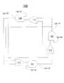
- FIG. 1Aillustrates an exemplary three state latch 100 , in accordance with embodiments of the present invention.
- Three state latch 100comprises three inputs, 131 A, 132 B and 133 C, and three outputs, 121 X, 122 Y and 123 Z.
- Three state latch 100comprises three two-input NAND gates 101 , 102 and 103 , and three two-input OR gates, 111 , 112 and 113 .
- FIG. 1Billustrates an exemplary truth table 150 for three state latch 100 of FIG. 1A , in accordance with embodiments of the present invention.
- Setting input 131 A, 132 B or 133 C to zeroforces the corresponding output 121 X, 122 Y or 123 Z to one.
- setting input 133 C to zeroforces output 123 Z to one.
- setting an input to oneforces the corresponding output to zero if any other input is zero.
- embodiments in accordance with the present inventionoffer several advantages in comparison to a three state circuit based on multiple conventional, e.g., two-state, latches. For example, there are no transitory states.
- embodiments in accordance with the present inventionmay operate asynchronously, e.g., with unclocked handshaking signals.
- embodiments in accordance with the present inventiongenerally require fewer gates, less die area and are thus less expensive in comparison to the conventional art.
- embodiments in accordance with the present inventionwill generally operate faster, e.g., with fewer gate delays, than under the conventional art.
- the worst case delay from input to outputis two gate delays.
- three state latch 100may be constructed from instances of an “OR-AND-INVERT” (“OAI”) gate structure, which is logically (but not physically) equivalent to the illustrated pairs of cascaded gates.
- OAIOR-AND-INVERT
- symbolic gates 111 and 101together represent an OR gate 111 , followed by an AND gate followed by inversion, e.g., NAND gate 101 .
- a three state latchmay be formed from an “AND-OR-INVERT” (“AOI”) gate structure, with inversion of the truth table. Such embodiments are considered within the scope of the present invention.
- Latch 100 of FIG. 1Ais presented schematically as a logical combination of OR and NAND gates.
- Each pair of OR and NAND gatesmay be rendered as a single OR-AND-Invert (OAI) gate with an equivalent logical function.
- FIG. 1Cillustrates a logical equivalence between a combination of OR and NAND gates 198 , e.g., as illustrated in FIG. 1A , and an OAI gate 199 . While logically equivalent, e.g., gates 198 and gate 199 have the same truth table, it is appreciated that there are physical differences between two separate, cascaded gates as illustrated in 198 and a single OAI gate 199 .
- OAI gate 199will generally comprise fewer transistors, less die area, and operate faster and at less power consumption, in comparison to the 198 structure.
- OAI gate 199produces an output in a single gate delay, whereas gates 198 may generally be expected to require two gate delays to propagate a signal.
- embodiments in accordance with the present inventionmay utilize an OAI gate structure, e.g., OAI gate 199 , or an AOI gate structure.
- OAI gate structuree.g., OAI gate 199
- AOI gate structuree.g., OAI gate 199
- the schematic representations presented hereinillustrate the logical function of the separate gates.
- all inputs of OAI gate 199do not have the same logical function, and hence schematics utilizing the logical function of the separate gates represent a preferred approach to illustrate aspects of the present invention.
- inputs A and Bare referred to as OR inputs of the OAI gate 199 , and its schematic equivalent 198 .
- Input Cis referred to as a NAND input.
- latches with an arbitrary number of inputsmay be formed by “widening” the first part of the gate, e.g., the OR gate in the exemplary OAI gate structure.
- the OR gates of FIG. 1Ashould be changed to be three input gates.
- FIG. 2Aillustrates an exemplary four state latch 200 , in accordance with embodiments of the present invention.
- Four state latch 200comprises four inputs, 231 A, 232 B, 233 C and 234 D, and four outputs, 221 X, 222 Y, 223 Z and 224 W.
- Four state latch 200comprises four two-input NAND gates 201 , 202 , 203 and 204 , and four three-input OR gates, 211 , 212 , 213 and 214 .
- FIG. 2Billustrates an exemplary truth table 250 for four state latch 200 of FIG. 2A , in accordance with embodiments of the present invention.
- Setting input 231 A, 232 B, 233 C or 234 D to zeroforces the corresponding output 221 X, 222 Y, 223 Z or 224 W to one.
- setting input 233 C to zeroforces output 223 Z to one.
- outputs 221 X, 222 Y and 223 Zwill be zero, and output 224 W will be set to one.
- output 224 Wwill be set to one.
- outputsare cross coupled to logic accepting the other inputs.
- output 221 Xis coupled to OR gate 212 , a part of the logic accepting input 232 B, is coupled to OR gate 213 , a part of the logic accepting input 233 C, and is coupled to OR gate 214 , a part of the logic accepting input 234 D.
- the first gate of each stageshould have inputs for the number of states (stages) minus one.
- Embodiments in accordance with the present inventionprovide systems and methods for three state latches.
- embodiments in accordance with the present inventionprovide systems and methods for three state latches that store more than two states in a single latch circuit.
- embodiments in accordance with the present inventionprovide systems and methods for three state latches that store more than two states in a single latch circuit in a deterministic manner.
- embodiments in accordance with the present inventionprovide systems and methods for three state latches that store more than two states in a single latch circuit that are compatible and complementary with existing systems and methods of integrated circuit design, manufacturing and test.
Landscapes
- Engineering & Computer Science (AREA)
- Computer Hardware Design (AREA)
- Physics & Mathematics (AREA)
- Computing Systems (AREA)
- General Engineering & Computer Science (AREA)
- Mathematical Physics (AREA)
- Power Engineering (AREA)
- Microelectronics & Electronic Packaging (AREA)
- Logic Circuits (AREA)
Abstract
Description
This application is related to co-pending, commonly owned U.S. patent application Ser. No. 13/910,001, filed Jun. 4, 2013, entitled “Handshaking Sense Amplifier,” to Gotterba and Wang and to U.S. patent application Ser. No. 13/910,038, filed Jun. 4, 2013, entitled “Pipelined One Cycle Throughput for Single-Port 6T RAM,” to Wang and Gotterba. Both applications are hereby incorporated herein by reference in their entireties for all purposes.
Embodiments of the present invention relate to the field of integrated circuit design and operation. More specifically, embodiments of the present invention relate to systems and methods for three state latches.
The term “latch” conventionally is used to refer to or to describe an electronic circuit that has two stable states and may be used to store a value, e.g., a single bit of information. Latches may be used for a wide variety of circuit applications, including, for example, in finite state machines, as counters and for synchronizing signals. If more than two states, e.g., more than one bit of information, are required, it is common to combine two or more latches to represent the desired number of states.
Unfortunately, such multiple-latch circuits suffer from several deleterious drawbacks. For example, a multiple-latch circuit generally requires additional circuitry surrounding the latches to “interpret” the combined state of the latches, and to control the state changes of the multiple latches. Such additional circuitry may slow down the operation of the multiple-latch circuit. In addition, a multiple-latch circuit is less deterministic than a single latch. For example, while any single latch may be in a known state, a multiple-latch circuit may be in a variety of transitory states. For example, one latch of a multiple-latch circuit may operate faster than another, completing a state transition prior to another latch changing state. Additionally, the state of one latch may depend on the state of another latch, and thus cannot change until the other latch has completed its transition. Further, the state-control logic surrounding the multiple latches requires a finite time to command, control and/or report a combined state of the multiple latches, further introducing times at which a state of a multiple-latch circuit is indeterminate.
Therefore, what is needed are systems and methods for three state latches. What is additionally needed are systems and methods for three state latches that store more than two states in a single latch circuit. A further need is for systems and methods for three state latches that store more than two states in a single latch circuit in a deterministic manner. A still further need exists for systems and methods for three state latches that are compatible and complementary with existing systems and methods of integrated circuit design, manufacturing and test. Embodiments of the present invention provide these advantages.
In accordance with a first embodiment of the present invention, an electronic circuit includes a single latch having three stable states. The electronic circuit may be configured so that all three outputs reflect a change at any one input in not more than three gate delays. The electronic circuit may further be configured so that when all inputs are set to one, a previous state of the latch is retained and output on the outputs.
In accordance with another embodiment of the present invention, an electronic circuit includes n pairs of cascaded logical gates, wherein each of the n pairs of cascaded logical gates includes a first logical gate comprising n−1 first gate inputs and one first gate output, and a second logical gate comprising two second gate inputs and one second gate output. One of the second gate inputs is coupled to the first gate output. The second gate output is cross coupled to one of the first gate inputs of all other pairs of cascaded gates. The value of n is greater than two. The pairs of cascaded gates may be rendered as a single OR-AND-Invert (OAI) gate.
In accordance with a further embodiment of the present invention, an electronic circuit includes a single latch circuit. The single latch circuit includes a first OR-AND-Invert gate having an output coupled to an OR input of a second OAI gate and to an OR input of a third OAI gate. The second OR-AND-Invert gate has an output coupled to an OR input of the first OAI gate and to an OR input of the third OAI gate. The third OR-AND-Invert gate has an output coupled to an OR input of the first OAI gate and to an OR input of the second OAI gate.
The accompanying drawings, which are incorporated in and form a part of this specification, illustrate embodiments of the invention and, together with the description, serve to explain the principles of the invention. Unless otherwise noted, the drawings are not drawn to scale.
Reference will now be made in detail to various embodiments of the present invention, examples of which are illustrated in the accompanying drawings. While the invention will be described in conjunction with these embodiments, it is understood that they are not intended to limit the invention to these embodiments. On the contrary, the invention is intended to cover alternatives, modifications and equivalents, which may be included within the spirit and scope of the invention as defined by the appended claims. Furthermore, in the following detailed description of the invention, numerous specific details are set forth in order to provide a thorough understanding of the invention. However, it will be recognized by one of ordinary skill in the art that the invention may be practiced without these specific details. In other instances, well known methods, procedures, components, and circuits have not been described in detail as not to unnecessarily obscure aspects of the invention.
It is to be appreciated that the term “three state” as used herein does not refer to, and is not analogous to the term “Tri-State®,” a registered trademark of Texas Instruments, Inc., of Dallas, Tex. As is known to those of skill in the art, a Tri-State® device includes conventional “high” and “low” outputs, as well as a high impedance, or “hi-Z,” output state. Embodiments in accordance with the present invention store three (or more) states in a single latch.
If all inputs131 A,132 B and133 C are set to one, then the output oflatch 100 will retain the state it had last, as indicated by the last row of truth table150. The “star” notation, e.g., “X*,” indicates previous state of the output signal line. For example, if inputs131 A and132 B are set to one, and input133 C is set to zero, outputs121 X and122 Y will be zero, and output123 Z will be set to one. Changing input133 C from zero to one will result in all inputs set to one, and the outputs will retain their previous state. In this example, outputs121 X and122 Y will be zero, and output123 Z will be set to one. In accordance with embodiments of the present invention, which ever input is the last to transition from zero to one will have its output remain one.
It is appreciated that embodiments in accordance with the present invention offer several advantages in comparison to a three state circuit based on multiple conventional, e.g., two-state, latches. For example, there are no transitory states. In addition, embodiments in accordance with the present invention may operate asynchronously, e.g., with unclocked handshaking signals. Further, further, embodiments in accordance with the present invention generally require fewer gates, less die area and are thus less expensive in comparison to the conventional art. Still further, embodiments in accordance with the present invention will generally operate faster, e.g., with fewer gate delays, than under the conventional art. For example, in accordance with embodiments of the present invention, the worst case delay from input to output is two gate delays.
It is appreciated that three state latch100 (FIG. 1 ) may be constructed from instances of an “OR-AND-INVERT” (“OAI”) gate structure, which is logically (but not physically) equivalent to the illustrated pairs of cascaded gates. For example,symbolic gates gate 111, followed by an AND gate followed by inversion, e.g.,NAND gate 101. In accordance with embodiments of the present invention, a three state latch may be formed from an “AND-OR-INVERT” (“AOI”) gate structure, with inversion of the truth table. Such embodiments are considered within the scope of the present invention.
Latch100 ofFIG. 1A is presented schematically as a logical combination of OR and NAND gates. Each pair of OR and NAND gates may be rendered as a single OR-AND-Invert (OAI) gate with an equivalent logical function.FIG. 1C illustrates a logical equivalence between a combination of OR andNAND gates 198, e.g., as illustrated inFIG. 1A , and anOAI gate 199. While logically equivalent, e.g.,gates 198 andgate 199 have the same truth table, it is appreciated that there are physical differences between two separate, cascaded gates as illustrated in198 and asingle OAI gate 199. For example,OAI gate 199 will generally comprise fewer transistors, less die area, and operate faster and at less power consumption, in comparison to the198 structure. For example,OAI gate 199 produces an output in a single gate delay, whereasgates 198 may generally be expected to require two gate delays to propagate a signal.
Accordingly, embodiments in accordance with the present invention may utilize an OAI gate structure, e.g.,OAI gate 199, or an AOI gate structure. However, the schematic representations presented herein illustrate the logical function of the separate gates. For example, all inputs ofOAI gate 199 do not have the same logical function, and hence schematics utilizing the logical function of the separate gates represent a preferred approach to illustrate aspects of the present invention. With reference toFIG. 1C , inputs A and B are referred to as OR inputs of theOAI gate 199, and itsschematic equivalent 198. Input C is referred to as a NAND input.
In addition, in accordance with embodiments of the present invention, latches with an arbitrary number of inputs may be formed by “widening” the first part of the gate, e.g., the OR gate in the exemplary OAI gate structure. For example, to form a four-input latch, the OR gates ofFIG. 1A should be changed to be three input gates.
If all inputs231 A,232 B,233 C and234 D are set to one, then the output oflatch 200 will retain the state it had last, as indicated by the last row of truth table250. The “star” notation, e.g., “X*,” indicates previous state of the output signal line. For example, if inputs231 A,232 B, and233 C are set to one, and input234 D is set to zero, outputs221 X,222 Y and223 Z will be zero, and output224 W will be set to one. Changing input234 D from zero to one will result in all inputs set to one, and the outputs will retain their previous state. In this example, outputs221 X,222 Y and223 Z will be zero, and output224 W will be set to one. In accordance with embodiments of the present invention, which ever input is the last to transition from zero to one will have its output remain one.
As illustrated in threestate latch 100 ofFIG. 1A and fourstate latch 200 ofFIG. 2A , all outputs are cross coupled to logic accepting the other inputs. For example, with respect to fourstate latch 200 ofFIG. 2A , output221 X is coupled to ORgate 212, a part of the logic accepting input232 B, is coupled to ORgate 213, a part of the logic accepting input233 C, and is coupled to ORgate 214, a part of thelogic accepting input 234 D. Accordingly, the first gate of each stage should have inputs for the number of states (stages) minus one.
Embodiments in accordance with the present invention provide systems and methods for three state latches. In addition, embodiments in accordance with the present invention provide systems and methods for three state latches that store more than two states in a single latch circuit. Further, embodiments in accordance with the present invention provide systems and methods for three state latches that store more than two states in a single latch circuit in a deterministic manner. Still further, embodiments in accordance with the present invention provide systems and methods for three state latches that store more than two states in a single latch circuit that are compatible and complementary with existing systems and methods of integrated circuit design, manufacturing and test.
Various embodiments of the invention are thus described. While the present invention has been described in particular embodiments, it should be appreciated that the invention should not be construed as limited by such embodiments, but rather construed according to the below claims.
Claims (20)
1. An electronic circuit comprising a single latch having three stable states, said latch comprising three inputs and three outputs for indicating said three stable states, and wherein said latch is configured wherein all said three outputs reflect a change at any one of said inputs in not more than two gate delays.
2. The electronic circuit ofclaim 1 wherein the three inputs are for controlling said three stable states.
3. The electronic circuit ofclaim 1 configured wherein a zero on an input forces a corresponding output to one.
4. The electronic circuit ofclaim 1 configured wherein a one on less than all inputs forces a corresponding output to zero.
5. The electronic circuit ofclaim 1 configured wherein when all inputs are set to one, a previous state of the latch is retained and output on said outputs.
6. The electronic circuit ofclaim 1 wherein said single latch circuit is configured to operate without a clock signal.
7. The electronic circuit ofclaim 1 wherein said single latch circuit has no transitory states.
8. The electronic circuit ofclaim 1 wherein said single latch circuit comprises a maximum of 18 transistors.
9. An electronic circuit comprising:
a single latch having 2n−1 stable states, said latch comprising:
n outputs for indicating said 2n−1 stable states,
wherein n is an integer greater than 2.
10. The electronic circuit ofclaim 9 comprising exactly n outputs for indicating said 2n−1 stable states.
11. The electronic circuit ofclaim 9 wherein said latch is configured wherein all said n outputs reflect a change at any one input in not more than two gate delays.
12. The electronic circuit ofclaim 9 further comprising n inputs for controlling said 2n−1 stable states.
13. The electronic circuit ofclaim 12 configured so that a zero on an input forces a corresponding output to one.
14. The electronic circuit ofclaim 12 configured so that a one on less than all inputs forces a corresponding output to zero.
15. The electronic circuit ofclaim 12 configured so that when all inputs are set to one, a previous state of the latch is retained and output on said outputs.
16. An electronic circuit comprising a single latch having n stable states, said latch comprising n outputs for indicating said n stable states, and wherein said latch is configured wherein all said n outputs reflect a change at any one input in not more than two gate delays, wherein n is an integer greater than 3.
17. The electronic circuit ofclaim 16 comprising n inputs for controlling said n stable states.
18. The electronic circuit ofclaim 16 configured wherein a zero on an input forces a corresponding output to one.
19. The electronic circuit ofclaim 16 configured wherein a one on less than all inputs forces a corresponding output to zero.
20. The electronic circuit ofclaim 16 configured wherein when all inputs are set to one, a previous state of the latch is retained and output on said outputs.
Priority Applications (2)
| Application Number | Priority Date | Filing Date | Title |
|---|---|---|---|
| US13/909,981US10141930B2 (en) | 2013-06-04 | 2013-06-04 | Three state latch |
| US15/476,847US10009027B2 (en) | 2013-06-04 | 2017-03-31 | Three state latch |
Applications Claiming Priority (1)
| Application Number | Priority Date | Filing Date | Title |
|---|---|---|---|
| US13/909,981US10141930B2 (en) | 2013-06-04 | 2013-06-04 | Three state latch |
Related Child Applications (1)
| Application Number | Title | Priority Date | Filing Date |
|---|---|---|---|
| US15/476,847DivisionUS10009027B2 (en) | 2013-06-04 | 2017-03-31 | Three state latch |
Publications (2)
| Publication Number | Publication Date |
|---|---|
| US20140354330A1 US20140354330A1 (en) | 2014-12-04 |
| US10141930B2true US10141930B2 (en) | 2018-11-27 |
Family
ID=51984420
Family Applications (2)
| Application Number | Title | Priority Date | Filing Date |
|---|---|---|---|
| US13/909,981Active2034-04-19US10141930B2 (en) | 2013-06-04 | 2013-06-04 | Three state latch |
| US15/476,847ActiveUS10009027B2 (en) | 2013-06-04 | 2017-03-31 | Three state latch |
Family Applications After (1)
| Application Number | Title | Priority Date | Filing Date |
|---|---|---|---|
| US15/476,847ActiveUS10009027B2 (en) | 2013-06-04 | 2017-03-31 | Three state latch |
Country Status (1)
| Country | Link |
|---|---|
| US (2) | US10141930B2 (en) |
Families Citing this family (6)
| Publication number | Priority date | Publication date | Assignee | Title |
|---|---|---|---|---|
| US9911470B2 (en) | 2011-12-15 | 2018-03-06 | Nvidia Corporation | Fast-bypass memory circuit |
| CN103632712A (en) | 2012-08-27 | 2014-03-12 | 辉达公司 | Memory cell and memory |
| US9685207B2 (en) | 2012-12-04 | 2017-06-20 | Nvidia Corporation | Sequential access memory with master-slave latch pairs and method of operating |
| US10141930B2 (en) | 2013-06-04 | 2018-11-27 | Nvidia Corporation | Three state latch |
| US9418730B2 (en) | 2013-06-04 | 2016-08-16 | Nvidia Corporation | Handshaking sense amplifier |
| US9418714B2 (en) | 2013-07-12 | 2016-08-16 | Nvidia Corporation | Sense amplifier with transistor threshold compensation |
Citations (116)
| Publication number | Priority date | Publication date | Assignee | Title |
|---|---|---|---|---|
| US3178590A (en)* | 1962-04-02 | 1965-04-13 | Ibm | Multistate memory circuit employing at least three logic elements |
| US3241122A (en)* | 1961-07-07 | 1966-03-15 | Ibm | Asynchronous data processing circuits |
| US3252004A (en)* | 1962-11-28 | 1966-05-17 | Ibm | Multistate memory circuit |
| US3381232A (en)* | 1964-12-02 | 1968-04-30 | Ibm | Gated latch |
| US3413557A (en)* | 1965-07-02 | 1968-11-26 | Ibm | Gated strobing latch for synchronizing data in an asynchronous system |
| US3444470A (en)* | 1966-01-13 | 1969-05-13 | Ibm | Pulse discriminating latch |
| US3474262A (en)* | 1966-03-30 | 1969-10-21 | Sperry Rand Corp | N-state control circuit |
| US3909634A (en)* | 1971-02-05 | 1975-09-30 | Ibm | Three state latch |
| US4076299A (en)* | 1976-06-18 | 1978-02-28 | Westran Corporation | Detachable truck body |
| US4107549A (en)* | 1977-05-10 | 1978-08-15 | Moufah Hussein T | Ternary logic circuits with CMOS integrated circuits |
| US4256411A (en) | 1978-12-15 | 1981-03-17 | National Blank Book Company, Inc. | File folder with integral loose leaf binder rings |
| US5032708A (en) | 1989-08-10 | 1991-07-16 | International Business Machines Corp. | Write-once-read-once batteryless authentication token |
| US5262973A (en) | 1992-03-13 | 1993-11-16 | Sun Microsystems, Inc. | Method and apparatus for optimizing complex arithmetic units for trivial operands |
| US5305258A (en) | 1990-08-30 | 1994-04-19 | Nippon Steel Corporation | Semiconductor memory and memory cell |
| US5349255A (en) | 1993-03-08 | 1994-09-20 | Altera Corporation | Programmable tco circuit |
| US5422805A (en) | 1992-10-21 | 1995-06-06 | Motorola, Inc. | Method and apparatus for multiplying two numbers using signed arithmetic |
| US5586081A (en) | 1994-06-03 | 1996-12-17 | Intel Corporation | Synchronous address latching for memory arrays |
| US5586069A (en) | 1994-09-30 | 1996-12-17 | Vlsi Technology, Inc. | Arithmetic logic unit with zero sum prediction |
| US5615113A (en) | 1995-06-16 | 1997-03-25 | Cyrix Corporation | Early signaling of no-overflow for nonrestoring twos complement division |
| US5638312A (en) | 1995-03-03 | 1997-06-10 | Hal Computer Systems, Inc. | Method and apparatus for generating a zero bit status flag in a microprocessor |
| US5748515A (en) | 1996-09-23 | 1998-05-05 | Advanced Risc Machines Limited | Data processing condition code flags |
| US5821791A (en) | 1995-10-12 | 1998-10-13 | Sgs-Thomson Microelectronics S.R.L. | Low-consumption and high-density D flip-flop circuit implementation particularly for standard cell libraries |
| US5867443A (en) | 1995-08-17 | 1999-02-02 | The United States Of America As Represented By The Secretary Of The Air Force | Shared bitline heterogeneous memory |
| US5903171A (en) | 1997-05-29 | 1999-05-11 | Winbond Electronics Corporation | Sense amplifier with integrated latch and level shift |
| US5949706A (en) | 1993-03-01 | 1999-09-07 | Motorola, Inc. | Static random access memory cell having a thin film transistor (TFT) pass gate connection to a bit line |
| US6009451A (en) | 1996-11-22 | 1999-12-28 | Lucent Technologies Inc. | Method for generating barrel shifter result flags directly from input data |
| US6041008A (en) | 1998-05-13 | 2000-03-21 | Micron Technology Inc. | Method and apparatus for embedded read only memory in static random access memory |
| US6118304A (en)* | 1997-11-20 | 2000-09-12 | Intrinsity, Inc. | Method and apparatus for logic synchronization |
| US6125064A (en) | 1998-11-13 | 2000-09-26 | Hyundai Micro Electronics Co., Ltd. | CAS latency control circuit |
| US6133754A (en)* | 1998-05-29 | 2000-10-17 | Edo, Llc | Multiple-valued logic circuit architecture; supplementary symmetrical logic circuit structure (SUS-LOC) |
| US6173303B1 (en) | 1998-11-06 | 2001-01-09 | National Semiconductor Corp. | Multiply circuit and method that detects portions of operands whose partial products are superfluous and modifies partial product manipulation accordingly |
| US6300809B1 (en) | 2000-07-14 | 2001-10-09 | International Business Machines Corporation | Double-edge-triggered flip-flop providing two data transitions per clock cycle |
| US6304505B1 (en) | 2000-05-22 | 2001-10-16 | Micron Technology Inc. | Differential correlated double sampling DRAM sense amplifier |
| US6310501B1 (en) | 1998-11-27 | 2001-10-30 | Nec Corporation | Latch circuit for latching data at an edge of a clock signal |
| US6396309B1 (en) | 2001-04-02 | 2002-05-28 | Intel Corporation | Clocked sense amplifier flip flop with keepers to prevent floating nodes |
| US20020089364A1 (en)* | 2000-11-10 | 2002-07-11 | Goldgeisser Leonid B. | MOS latch with three stable operating points |
| US6438024B1 (en) | 2001-01-11 | 2002-08-20 | Sun Microsystems, Inc. | Combining RAM and ROM into a single memory array |
| US6442721B2 (en) | 1996-10-18 | 2002-08-27 | Texas Instruments Incorporated | Accelerating scan test by re-using response data as stimulus data |
| US6452433B1 (en) | 2000-05-31 | 2002-09-17 | Conexant Systems, Inc. | High phase margin low power flip-flop |
| US6472920B1 (en) | 2001-09-17 | 2002-10-29 | Agere Systems Inc. | High speed latch circuit |
| US20020158663A1 (en)* | 2000-05-25 | 2002-10-31 | Eliahu Shemesh | Non-binary digital logic element and circuit design therefor |
| US6501677B1 (en) | 1998-02-25 | 2002-12-31 | Xilinx, Inc. | Configuration memory architecture for FPGA |
| US6580411B1 (en) | 1998-04-28 | 2003-06-17 | Sharp Kabushiki Kaisha | Latch circuit, shift register circuit and image display device operated with a low consumption of power |
| US20030117170A1 (en)* | 2001-12-20 | 2003-06-26 | Sun Microsystems, Inc. | Method and apparatus for performing a hazard-free multi-bit comparsion |
| US20030123320A1 (en) | 1997-04-25 | 2003-07-03 | Wright Jeffrey P. | Synchronous dynamic random access memory device |
| US20030156461A1 (en) | 2000-07-07 | 2003-08-21 | Paul Demone | Method and apparatus for simultaneous differential data sensing and capture in a high speed memory |
| US6630853B1 (en) | 2002-07-23 | 2003-10-07 | Kabushiki Kaisha Toshiba | Semiconductor integrated circuit including conditional clocking flip-flop circuit |
| US6646938B2 (en)* | 2001-07-25 | 2003-11-11 | Fujitsu Limited | Static memory having self-timing circuit |
| US20030210078A1 (en) | 2002-05-08 | 2003-11-13 | University Of Southern California | Current source evaluation sense-amplifier |
| US20040027184A1 (en) | 2002-08-06 | 2004-02-12 | Mitsubishi Denki Kabushiki Kaisha | Master slave flip-flop circuit functioning as edge trigger flip-flop |
| US6747485B1 (en) | 2000-06-28 | 2004-06-08 | Sun Microsystems, Inc. | Sense amplifier type input receiver with improved clk to Q |
| JP2004214997A (en) | 2002-12-27 | 2004-07-29 | Sony Corp | Flip-flop |
| US6771104B2 (en)* | 2002-07-25 | 2004-08-03 | Koninklijke Philips Electronics N.V. | Switching electronic circuit for random number generation |
| US20040160244A1 (en) | 2002-08-07 | 2004-08-19 | Samsung Electronics Co., Ltd | Sense amplifier having synchronous reset or asynchronous reset capability |
| US20040243896A1 (en) | 2003-05-13 | 2004-12-02 | Intel Corporation | Test scan cells |
| US6842059B1 (en) | 2003-04-21 | 2005-01-11 | Pericom Semiconductor Corp. | Muxed-output double-date-rate-2 (DDR2) register with fast propagation delay |
| US20050040856A1 (en) | 2003-08-22 | 2005-02-24 | Ravindraraj Ramaraju | Domino circuitry compatible static latch |
| US20050108604A1 (en) | 2003-11-14 | 2005-05-19 | Wong Tak K. | Scan chain registers that utilize feedback paths within latch units to support toggling of latch unit outputs during enhanced delay fault testing |
| US20050128844A1 (en) | 2003-12-15 | 2005-06-16 | Matsushita Elec. Ind. Co. Ltd. | Semiconductor integrated circuit |
| US6924683B1 (en) | 2003-12-19 | 2005-08-02 | Integrated Device Technology, Inc. | Edge accelerated sense amplifier flip-flop with high fanout drive capability |
| US20050278661A1 (en)* | 2004-06-01 | 2005-12-15 | Peter Lablans | Multi-valued digital information retaining elements and memory devices |
| US20060049852A1 (en) | 2004-09-09 | 2006-03-09 | In-Soo Park | Sense amplifier with low common mode differential input signal |
| US7051169B2 (en) | 2002-02-26 | 2006-05-23 | Kyocera Wireless Corp. | Memory configuration for a wireless communications device |
| US7057421B2 (en) | 2004-04-22 | 2006-06-06 | Winbond Electronics Corp. | Flipflop |
| US7111133B2 (en) | 2001-05-18 | 2006-09-19 | Hitachi, Ltd. | Control apparatus for selectively operating with program data from two memories and having a system controller supplying program data and address for writing the data to the second memory |
| US20070028157A1 (en) | 2005-07-28 | 2007-02-01 | Drake Alan J | Self-resetting, self-correcting latches |
| US7196552B2 (en) | 2005-04-12 | 2007-03-27 | Hewlett-Packard Development Company, L.P. | Comparator circuit with offset cancellation |
| US7227798B2 (en) | 2002-10-07 | 2007-06-05 | Stmicroelectronics Pvt. Ltd. | Latch-type sense amplifier |
| US20070130242A1 (en) | 2005-12-02 | 2007-06-07 | Fujitsu Limited | Arithmetic operation unit, information processing apparatus and arithmetic operation method |
| US20070146033A1 (en) | 2005-12-16 | 2007-06-28 | Infineon Technologies Ag | Circuit arrangement and method for operating a circuit arrangement |
| US7242235B1 (en) | 2005-02-25 | 2007-07-10 | Exar Corporation | Dual data rate flip-flop |
| US20070180006A1 (en) | 2006-01-31 | 2007-08-02 | Renesas Technology Corp. | Parallel operational processing device |
| US20070253263A1 (en) | 2006-04-28 | 2007-11-01 | Nscore Inc. | Nonvolatile memory device with test mechanism |
| US7304903B2 (en) | 2006-01-23 | 2007-12-04 | Purdue Research Foundation | Sense amplifier circuit |
| US7333516B1 (en) | 2000-07-20 | 2008-02-19 | Silicon Graphics, Inc. | Interface for synchronous data transfer between domains clocked at different frequencies |
| US20080086667A1 (en) | 2006-10-05 | 2008-04-10 | Princeton Technology Corporation | Chip testing device and system |
| US7405606B2 (en) | 2006-04-03 | 2008-07-29 | Intellectual Ventures Fund 27 Llc | D flip-flop |
| US7408393B1 (en) | 2007-03-08 | 2008-08-05 | Inphi Corporation | Master-slave flip-flop and clocking scheme |
| US20080195337A1 (en) | 2007-02-09 | 2008-08-14 | Agarwal Kanak B | Scannable Virtual Rail Method and Ring Oscillator Circuit for Measuring Variations in Device Characteristics |
| US20090040848A1 (en) | 2007-08-09 | 2009-02-12 | Tadashi Nitta | Semiconductor memory device |
| US7498850B2 (en) | 2007-06-22 | 2009-03-03 | Intel Corporation | Compensated comparator for use in lower voltage, higher speed non-volatile memory |
| US7499347B2 (en) | 2006-08-09 | 2009-03-03 | Qualcomm Incorporated | Self-timing circuit with programmable delay and programmable accelerator circuits |
| US20090168499A1 (en) | 2007-12-28 | 2009-07-02 | Kabushiki Kaisha Toshiba | Semiconductor memory device |
| US7613030B2 (en) | 2005-11-25 | 2009-11-03 | Semiconductor Energy Laboratory Co., Ltd. | Semiconductor memory device and method for operating the same |
| US20100102890A1 (en) | 2008-10-27 | 2010-04-29 | Asic North, Inc. | Variable-Loop-Path Ring Oscillator Test Circuit and Systems and Methods Utilizing Same |
| US20100109707A1 (en) | 2008-11-03 | 2010-05-06 | Freescale Semiconductror, Inc | Low power, self-gated, pulse triggered clock gating cell |
| US7724606B2 (en) | 2006-08-03 | 2010-05-25 | Renesas Technology Corp. | Interface circuit |
| US7760117B1 (en) | 2009-01-16 | 2010-07-20 | Mediatek Inc. | Flip-flop and pipelined analog-to-digital converter utilizing the same |
| US20100332924A1 (en) | 2009-06-30 | 2010-12-30 | Ziaja Thomas A | At-speed scan testing of memory arrays |
| US20110066904A1 (en) | 2009-09-11 | 2011-03-17 | International Business Machines Corporation | Avoiding race conditions at clock domain crossings in an edge based scan design |
| US20110168875A1 (en) | 2002-12-13 | 2011-07-14 | Renesas Electronics Corporation | Semiconductor integrated circuit and ic card system |
| US8164934B2 (en) | 2006-04-25 | 2012-04-24 | Renesas Electronics Corporation | Content addressable memory |
| US20120147680A1 (en) | 2009-09-02 | 2012-06-14 | Panasonic Corporation | Semiconductor memory device |
| US20120163068A1 (en) | 2009-08-24 | 2012-06-28 | Texas Instruments Incorporated | 10T SRAM Cell with Near Dual Port Functionality |
| US20120182056A1 (en) | 2011-01-18 | 2012-07-19 | Nvidia Corporation | Low energy flip-flops |
| US8330517B1 (en)* | 2010-12-21 | 2012-12-11 | Xilinx, Inc. | Bistable circuit with metastability resistance |
| US8332957B2 (en) | 2007-03-26 | 2012-12-11 | Teac Corporation | Storage device |
| US8352530B2 (en) | 2008-12-08 | 2013-01-08 | International Business Machines Corporation | Residue calculation with built-in correction in a floating point unit positioned at different levels using correction values provided by multiplexer |
| US8363492B2 (en) | 2009-05-27 | 2013-01-29 | Panasonic Corporation | Delay adjustment device and delay adjustment method |
| US8369177B2 (en) | 2010-03-05 | 2013-02-05 | Micron Technology, Inc. | Techniques for reading from and/or writing to a semiconductor memory device |
| US20130080740A1 (en) | 2011-09-28 | 2013-03-28 | Nvidia Corporation | Fast condition code generation for arithmetic logic unit |
| US20130129083A1 (en) | 2010-07-28 | 2013-05-23 | The Ritsumeikan Trust | Tamper-resistant memory integrated circuit and encryption circuit using same |
| US8453096B2 (en) | 2011-01-28 | 2013-05-28 | Lsi Corporation | Non-linear common coarse delay system and method for delaying data strobe |
| US20130155783A1 (en) | 2011-12-15 | 2013-06-20 | Nvidia Corporation | Fast-bypass memory circuit |
| US20130155781A1 (en) | 2011-12-15 | 2013-06-20 | Nvidia Corporation | Fast-bypass memory circuit |
| US8565034B1 (en) | 2011-09-30 | 2013-10-22 | Altera Corporation | Variation compensation circuitry for memory interface |
| US8570818B2 (en) | 2008-03-13 | 2013-10-29 | Qualcomm Incorporated | Address multiplexing in pseudo-dual port memory |
| US20140003160A1 (en)* | 2012-06-28 | 2014-01-02 | Lsi Corporation | High-Speed Sensing Scheme for Memory |
| US20140056050A1 (en) | 2012-08-27 | 2014-02-27 | Jun Yang | Memory cell and memory |
| US8760208B2 (en)* | 2012-03-30 | 2014-06-24 | Intel Corporation | Latch with a feedback circuit |
| US8830766B2 (en)* | 2013-01-23 | 2014-09-09 | Lsi Corporation | Margin free PVT tolerant fast self-timed sense amplifier reset circuit |
| US20140355362A1 (en) | 2013-06-04 | 2014-12-04 | Nvidia Corporation | Pipelined one cycle throughput for single-port 6t ram |
| US8908449B1 (en) | 2013-09-10 | 2014-12-09 | Freescale Semiconductor, Inc. | Master-slave flip-flop with reduced setup time |
| US20150016183A1 (en) | 2013-07-12 | 2015-01-15 | Nvidia Corporation | Sense amplifier with transistor threshold compensation |
| US8964457B2 (en) | 2012-11-30 | 2015-02-24 | Taiwan Semiconductor Manufacturing Company, Ltd. | Methods for operating SRAM cells |
| US20160269002A1 (en) | 2015-03-11 | 2016-09-15 | Nvidia Corporation | Low clocking power flip-flop |
Family Cites Families (128)
| Publication number | Priority date | Publication date | Assignee | Title |
|---|---|---|---|---|
| US3252001A (en) | 1961-11-29 | 1966-05-17 | Westinghouse Electric Corp | Vibration detection apparatus |
| US3421026A (en) | 1964-06-29 | 1969-01-07 | Gen Electric | Memory flip-flop |
| US3444480A (en) | 1967-08-09 | 1969-05-13 | Hewlett Packard Co | High frequency oscillator employing a transmission line having an electrically adjustable section of ground plane |
| US3539938A (en)* | 1968-12-30 | 1970-11-10 | North American Rockwell | Closed loop logic gate multiple phase clock signal generator |
| US3757231A (en)* | 1969-04-16 | 1973-09-04 | Dyad Systems Inc | Asynchronous circuit and system |
| US3760170A (en)* | 1971-03-19 | 1973-09-18 | Cam Technology Inc | Method and apparatus for automatic control |
| US3760167A (en)* | 1972-03-16 | 1973-09-18 | Honeywell Inf Systems | Phase jitter special purpose computer |
| GB2040625A (en)* | 1979-01-23 | 1980-08-28 | Nat Res Dev | Serial data logic circuit |
| US4544851A (en)* | 1981-08-31 | 1985-10-01 | Texas Instruments Incorporated | Synchronizer circuit with dual input |
| US4587480A (en)* | 1982-06-17 | 1986-05-06 | Storage Technology Partners | Delay testing method for CMOS LSI and VLSI integrated circuits |
| US4680484A (en)* | 1984-10-19 | 1987-07-14 | Trw Inc. | Wired-AND FET logic gate |
| US5319453A (en) | 1989-06-22 | 1994-06-07 | Airtrax | Method and apparatus for video signal encoding, decoding and monitoring |
| US5124804A (en) | 1990-09-10 | 1992-06-23 | Ncr Corporation | Programmable resolution video controller |
| US5121003A (en)* | 1990-10-10 | 1992-06-09 | Hal Computer Systems, Inc. | Zero overhead self-timed iterative logic |
| US5124084A (en) | 1991-01-04 | 1992-06-23 | Arctco, Inc. | Carburetor drain apparatus |
| US5140174A (en)* | 1991-01-25 | 1992-08-18 | Hewlett-Packard Co. | Symmetric edge true/complement buffer/inverter and method therefor |
| US5448257A (en) | 1991-07-18 | 1995-09-05 | Chips And Technologies, Inc. | Frame buffer with matched frame rate |
| DE69315010T2 (en)* | 1992-08-20 | 1998-04-16 | Koninkl Philips Electronics Nv | Oscillator with multi-phase outputs |
| US5600598A (en) | 1994-12-14 | 1997-02-04 | Mosaid Technologies Incorporated | Memory cell and wordline driver for embedded DRAM in ASIC process |
| US5696990A (en) | 1995-05-15 | 1997-12-09 | Nvidia Corporation | Method and apparatus for providing improved flow control for input/output operations in a computer system having a FIFO circuit and an overflow storage area |
| US6173306B1 (en) | 1995-07-21 | 2001-01-09 | Emc Corporation | Dynamic load balancing |
| US6265894B1 (en) | 1995-10-13 | 2001-07-24 | Frederic Reblewski | Reconfigurable integrated circuit with integrated debugging facilities for use in an emulation system |
| US5835941A (en) | 1995-11-17 | 1998-11-10 | Micron Technology Inc. | Internally cached static random access memory architecture |
| US6374255B1 (en) | 1996-05-21 | 2002-04-16 | Immersion Corporation | Haptic authoring |
| US6055590A (en) | 1996-06-05 | 2000-04-25 | Compaq Computer Corporation | Bridge circuit comprising independent transaction buffers with control logic adapted to store overflow data in second buffer when transaction size exceeds the first buffer size |
| US6031388A (en)* | 1996-07-19 | 2000-02-29 | The Board Of Trustees Of The Leland Stanford Junior University | Postcharged interconnection speed-up circuit |
| US6005430A (en)* | 1997-02-28 | 1999-12-21 | Texas Instruments Incorporated | Clock skew circuit |
| CA2198839C (en) | 1997-02-28 | 2004-11-02 | Richard C. Foss | Enhanced asic process cell |
| EP0948763B1 (en) | 1997-07-31 | 2003-12-17 | Fujitsu Limited | Shock mount for hard disk drive in a portable computer |
| US6084856A (en) | 1997-12-18 | 2000-07-04 | Advanced Micro Devices, Inc. | Method and apparatus for adjusting overflow buffers and flow control watermark levels |
| GB2346278B (en) | 1997-12-22 | 2000-10-25 | Lsi Logic Corp | Controllable latch/register circuit |
| US9292111B2 (en) | 1998-01-26 | 2016-03-22 | Apple Inc. | Gesturing with a multipoint sensing device |
| US5978311A (en) | 1998-03-03 | 1999-11-02 | Micron Technology, Inc. | Memory with combined synchronous burst and bus efficient functionality |
| US6400735B1 (en) | 1998-06-22 | 2002-06-04 | Xilinx, Inc. | Glitchless delay line using gray code multiplexer |
| JP3336408B2 (en) | 1998-07-17 | 2002-10-21 | 株式会社アドバンスト・ディスプレイ | Liquid crystal display |
| US6263331B1 (en) | 1998-07-30 | 2001-07-17 | Unisys Corporation | Hybrid hash join process |
| US6263410B1 (en) | 1998-09-15 | 2001-07-17 | Industrial Technology Research Institute | Apparatus and method for asynchronous dual port FIFO |
| KR100301059B1 (en) | 1999-07-20 | 2001-11-01 | 윤종용 | Full CMOS SRAM cell |
| US20080209114A1 (en) | 1999-08-04 | 2008-08-28 | Super Talent Electronics, Inc. | Reliability High Endurance Non-Volatile Memory Device with Zone-Based Non-Volatile Memory File System |
| AUPQ555700A0 (en) | 2000-02-11 | 2000-03-02 | Canon Kabushiki Kaisha | Fifo overflow management |
| US7779359B2 (en) | 2000-08-08 | 2010-08-17 | The United States Of America As Represented By The Secretary Of The Army | Multifunction display design tool |
| US6366529B1 (en) | 2000-08-30 | 2002-04-02 | Texas Instruments Incorporated | Fast FiFo memory storage system |
| JP4776824B2 (en) | 2000-09-19 | 2011-09-21 | シャープ株式会社 | Optical recording medium and optical recording / reproducing apparatus |
| US7071994B2 (en) | 2001-01-04 | 2006-07-04 | Telisar Corporation | System and method for nondisruptively embedding an OFDM modulated data signal into a composite video signal |
| JP4040473B2 (en) | 2001-07-12 | 2008-01-30 | 三菱電機株式会社 | Mixer circuit |
| US6987775B1 (en) | 2001-08-15 | 2006-01-17 | Internet Machines Corp. | Variable size First In First Out (FIFO) memory with head and tail caching |
| JP3968499B2 (en) | 2001-10-17 | 2007-08-29 | ソニー株式会社 | Display device |
| WO2003042413A1 (en) | 2001-10-23 | 2003-05-22 | Steen Research, Llc | Method and compositions for processing poultry feathers |
| US6801991B2 (en) | 2001-12-21 | 2004-10-05 | Agere Systems Inc. | Method and apparatus for buffer partitioning without loss of data |
| US7411233B2 (en) | 2002-08-27 | 2008-08-12 | E-Phocus, Inc | Photoconductor-on-active-pixel (POAP) sensor utilizing a multi-layered radiation absorbing structure |
| US6803610B2 (en) | 2002-09-30 | 2004-10-12 | Mosaid Technologies Incorporated | Optimized memory cell physical arrangement |
| US7747917B2 (en) | 2002-10-07 | 2010-06-29 | Cirrus Logic, Inc. | Scan cells with minimized shoot-through and scan chains and integrated circuits using the same |
| US7441233B1 (en) | 2002-12-20 | 2008-10-21 | Borland Software Corporation | System and method providing status indication for long-running modal tasks |
| US6822908B1 (en) | 2003-05-08 | 2004-11-23 | Micron Technology, Inc. | Synchronous up/down address generator for burst mode read |
| US20050171879A1 (en) | 2004-02-02 | 2005-08-04 | Li-Lan Lin | Interactive counter service system for banks and similar finance organizations |
| US7401278B2 (en) | 2004-03-29 | 2008-07-15 | International Business Machines Corporation | Edge-triggered master + LSSD slave binary latch |
| US7026975B1 (en)* | 2004-03-29 | 2006-04-11 | Maxim Integrated Products, Inc. | High speed digital path for successive approximation analog-to-digital converters |
| US7106098B1 (en) | 2004-05-04 | 2006-09-12 | Xilinx, Inc. | Split FIFO configuration of block RAM |
| JP4117275B2 (en)* | 2004-08-17 | 2008-07-16 | エルピーダメモリ株式会社 | Semiconductor integrated circuit |
| US7613969B2 (en) | 2004-10-29 | 2009-11-03 | Cadence Design Systems, Inc. | Method and system for clock skew independent scan register chains |
| US7113048B2 (en)* | 2004-11-12 | 2006-09-26 | International Business Machines Corporation | Ultra high frequency ring oscillator with voltage controlled frequency capabilities |
| US7346861B1 (en) | 2004-12-02 | 2008-03-18 | Altera Corporation | Programmable logic devices with two-phase latch circuitry |
| US7187222B2 (en) | 2004-12-17 | 2007-03-06 | Seiko Epson Corporation | CMOS master/slave flip-flop with integrated multiplexor |
| US7882299B2 (en) | 2004-12-21 | 2011-02-01 | Sandisk Corporation | System and method for use of on-chip non-volatile memory write cache |
| DK1839030T3 (en) | 2005-01-17 | 2010-08-02 | Biophos Ag | Method and apparatus for measuring the dynamic parameters of particles |
| US7283404B2 (en) | 2005-02-11 | 2007-10-16 | International Business Machines Corporation | Content addressable memory including a dual mode cycle boundary latch |
| FR2889212B1 (en) | 2005-07-26 | 2007-09-07 | Seb Sa | IRONING APPARATUS COMPRISING A STEAM GENERATOR CONNECTED TO AN IRON AND A DEFROSTING BRUSH |
| US7630389B1 (en) | 2005-12-14 | 2009-12-08 | Nvidia Corporation | Multi-thread FIFO memory generator |
| US7603246B2 (en) | 2006-03-31 | 2009-10-13 | Nvidia Corporation | Data interface calibration |
| US7543205B2 (en) | 2006-04-27 | 2009-06-02 | Texas Instruments Incorporated | Control signal synchronization of a scannable storage circuit |
| US7992062B2 (en) | 2006-06-22 | 2011-08-02 | Qualcomm Incorporated | Logic device and method supporting scan test |
| US7783911B2 (en) | 2006-06-27 | 2010-08-24 | International Business Machines Corporation | Programmable bus driver launch delay/cycle delay to reduce elastic interface elasticity requirements |
| US7739538B2 (en) | 2006-06-27 | 2010-06-15 | International Business Machines Corporation | Double data rate chaining for synchronous DDR interfaces |
| US7477112B1 (en)* | 2006-08-16 | 2009-01-13 | Xilinx, Inc. | Structure for the main oscillator of a counter-controlled delay line |
| US10313505B2 (en) | 2006-09-06 | 2019-06-04 | Apple Inc. | Portable multifunction device, method, and graphical user interface for configuring and displaying widgets |
| CN101523474B (en) | 2006-09-29 | 2012-01-18 | 夏普株式会社 | Display device |
| US8352815B2 (en) | 2006-10-18 | 2013-01-08 | Arm Limited | Circuit and method operable in functional and diagnostic modes |
| US20080100597A1 (en) | 2006-10-25 | 2008-05-01 | Macrovision Corporation | Method and apparatus to improve playability in overscan areas of a TV display |
| US8094128B2 (en) | 2007-01-03 | 2012-01-10 | Apple Inc. | Channel scan logic |
| US7956847B2 (en) | 2007-01-05 | 2011-06-07 | Apple Inc. | Gestures for controlling, manipulating, and editing of media files using touch sensitive devices |
| WO2008142610A1 (en) | 2007-05-16 | 2008-11-27 | Nxp B.V. | Fifo buffer |
| SG189721A1 (en) | 2007-06-11 | 2013-05-31 | Cameron Int Corp | Gate-coating process |
| US20090119631A1 (en) | 2007-11-06 | 2009-05-07 | Jordi Cortadella | Variability-Aware Asynchronous Scheme for High-Performance Delay Matching |
| US20090164951A1 (en) | 2007-12-19 | 2009-06-25 | Nvidia Corporation | Input architecture for devices with small input areas and executing multiple applications |
| US7863909B2 (en) | 2008-03-04 | 2011-01-04 | Synaptics Incorporated | System and method for measuring a capacitance by transferring charge from a fixed source |
| US8754904B2 (en) | 2011-04-03 | 2014-06-17 | Lucidlogix Software Solutions, Ltd. | Virtualization method of vertical-synchronization in graphics systems |
| US8592697B2 (en) | 2008-09-10 | 2013-11-26 | Apple Inc. | Single-chip multi-stimulus sensor controller |
| JP5275741B2 (en) | 2008-10-14 | 2013-08-28 | 株式会社東海理化電機製作所 | Vehicle electronic key system |
| US8310464B2 (en) | 2008-10-16 | 2012-11-13 | Texas Instruments Incorporated | Simultaneous multiple location touch systems |
| US8497690B2 (en) | 2008-10-27 | 2013-07-30 | Microchip Technology Incorporated | Automated capacitive touch scan |
| TWI412987B (en) | 2008-11-28 | 2013-10-21 | Htc Corp | Portable electronic device and method for waking up the same through touch screen from sleep mode |
| JP2010160653A (en) | 2009-01-07 | 2010-07-22 | Renesas Electronics Corp | Ring buffer circuit and control circuit for the same |
| US8286106B2 (en) | 2009-03-13 | 2012-10-09 | Oracle America, Inc. | System and method for interacting with status information on a touch screen device |
| TWI437469B (en) | 2009-03-17 | 2014-05-11 | Inventec Appliances Corp | Electronic book apparatus and operating method thereof |
| TWI419034B (en) | 2009-04-03 | 2013-12-11 | Novatek Microelectronics Corp | A control method of detecting a touch event for a touch panel and related device |
| WO2011008499A2 (en) | 2009-06-30 | 2011-01-20 | Applied Materials, Inc. | Leak proof pad for cmp endpoint detection |
| US8127057B2 (en) | 2009-08-13 | 2012-02-28 | Advanced Micro Devices, Inc. | Multi-level buffering of transactional data |
| WO2011056997A1 (en) | 2009-11-04 | 2011-05-12 | Fabrus Llc | Methods for affinity maturation-based antibody optimization |
| TWI510979B (en) | 2009-11-23 | 2015-12-01 | Elan Microelectronics Corp | Passive Integrated Circuit Architecture and Its Control Method for Scanning Touch Panel |
| US9528715B2 (en) | 2009-12-02 | 2016-12-27 | Thomas David Aiken | Occupancy-based demand controlled ventilation system |
| US20110181519A1 (en) | 2010-01-26 | 2011-07-28 | Himax Technologies Limited | System and method of driving a touch screen |
| JP2011253292A (en) | 2010-06-01 | 2011-12-15 | Sony Corp | Information processing system, method and program |
| US8799815B2 (en) | 2010-07-30 | 2014-08-05 | Apple Inc. | Device, method, and graphical user interface for activating an item in a folder |
| US20120050206A1 (en) | 2010-08-29 | 2012-03-01 | David Welland | Multi-touch resolve mutual capacitance sensor |
| US20120054379A1 (en) | 2010-08-30 | 2012-03-01 | Kafai Leung | Low power multi-touch scan control system |
| US8941592B2 (en) | 2010-09-24 | 2015-01-27 | Intel Corporation | Techniques to control display activity |
| JP2012129888A (en) | 2010-12-16 | 2012-07-05 | Samsung Electronics Co Ltd | Image encoding apparatus and image encoding method |
| KR20120080049A (en) | 2011-01-06 | 2012-07-16 | 주식회사 팬택 | Touch interface system and method |
| CN102593113B (en) | 2011-01-10 | 2015-04-01 | 展晶科技(深圳)有限公司 | Light emitting diode packaging structure |
| KR20120089980A (en) | 2011-01-12 | 2012-08-16 | 엘지전자 주식회사 | Multimedia devie having operating system able to process multiple graphic data and method for controlling the same |
| US9317158B2 (en) | 2011-03-08 | 2016-04-19 | Synaptics Incorporated | Baseline management for input devices |
| JP5421312B2 (en) | 2011-03-09 | 2014-02-19 | 富士フイルム株式会社 | 3D display device and time-division 3D display system |
| JP5651058B2 (en) | 2011-03-30 | 2015-01-07 | ルネサスエレクトロニクス株式会社 | Scan flip-flop circuit, scan test circuit and control method thereof |
| US8681122B2 (en) | 2011-04-19 | 2014-03-25 | Cypress Semiconductor Corporation | Capacitive sensing with programmable logic for touch sense arrays |
| US20120268414A1 (en) | 2011-04-25 | 2012-10-25 | Motorola Mobility, Inc. | Method and apparatus for exchanging data with a user computer device |
| KR101863332B1 (en) | 2011-08-08 | 2018-06-01 | 삼성디스플레이 주식회사 | Scan driver, display device including the same and driving method thereof |
| US20130069894A1 (en) | 2011-09-16 | 2013-03-21 | Htc Corporation | Electronic device and method for driving a touch sensor thereof |
| US9677493B2 (en) | 2011-09-19 | 2017-06-13 | Honeywell Spol, S.R.O. | Coordinated engine and emissions control system |
| DE102012108810A1 (en) | 2011-09-20 | 2013-03-21 | Beijing Lenovo Software Ltd. | ELECTRONIC DEVICE AND CONDITION CONTROL SYSTEM |
| US8749289B2 (en)* | 2011-12-19 | 2014-06-10 | Intel Corporation | Multi-phase clock generation apparatus and method |
| US9342181B2 (en) | 2012-01-09 | 2016-05-17 | Nvidia Corporation | Touch-screen input/output device touch sensing techniques |
| US8981822B2 (en)* | 2012-09-14 | 2015-03-17 | Intel Corporation | High speed dual modulus divider |
| US20140129745A1 (en) | 2012-11-08 | 2014-05-08 | Nvidia Corporation | Asymmetric fifo memory |
| US20140156891A1 (en) | 2012-12-04 | 2014-06-05 | Nvidia Corporation | Systems and methods for automatically generating master-slave latch structures with fully registered flow control |
| US9281817B2 (en) | 2012-12-31 | 2016-03-08 | Nvidia Corporation | Power conservation using gray-coded address sequencing |
| US20140244921A1 (en) | 2013-02-26 | 2014-08-28 | Nvidia Corporation | Asymmetric multithreaded fifo memory |
| US10141930B2 (en) | 2013-06-04 | 2018-11-27 | Nvidia Corporation | Three state latch |
| US9418730B2 (en) | 2013-06-04 | 2016-08-16 | Nvidia Corporation | Handshaking sense amplifier |
- 2013
- 2013-06-04USUS13/909,981patent/US10141930B2/enactiveActive
- 2017
- 2017-03-31USUS15/476,847patent/US10009027B2/enactiveActive
Patent Citations (125)
| Publication number | Priority date | Publication date | Assignee | Title |
|---|---|---|---|---|
| US3241122A (en)* | 1961-07-07 | 1966-03-15 | Ibm | Asynchronous data processing circuits |
| US3178590A (en)* | 1962-04-02 | 1965-04-13 | Ibm | Multistate memory circuit employing at least three logic elements |
| US3252004A (en)* | 1962-11-28 | 1966-05-17 | Ibm | Multistate memory circuit |
| US3381232A (en)* | 1964-12-02 | 1968-04-30 | Ibm | Gated latch |
| US3413557A (en)* | 1965-07-02 | 1968-11-26 | Ibm | Gated strobing latch for synchronizing data in an asynchronous system |
| US3444470A (en)* | 1966-01-13 | 1969-05-13 | Ibm | Pulse discriminating latch |
| US3474262A (en)* | 1966-03-30 | 1969-10-21 | Sperry Rand Corp | N-state control circuit |
| US3909634A (en)* | 1971-02-05 | 1975-09-30 | Ibm | Three state latch |
| US4076299A (en)* | 1976-06-18 | 1978-02-28 | Westran Corporation | Detachable truck body |
| US4107549A (en)* | 1977-05-10 | 1978-08-15 | Moufah Hussein T | Ternary logic circuits with CMOS integrated circuits |
| US4256411A (en) | 1978-12-15 | 1981-03-17 | National Blank Book Company, Inc. | File folder with integral loose leaf binder rings |
| US5032708A (en) | 1989-08-10 | 1991-07-16 | International Business Machines Corp. | Write-once-read-once batteryless authentication token |
| US5305258A (en) | 1990-08-30 | 1994-04-19 | Nippon Steel Corporation | Semiconductor memory and memory cell |
| US5262973A (en) | 1992-03-13 | 1993-11-16 | Sun Microsystems, Inc. | Method and apparatus for optimizing complex arithmetic units for trivial operands |
| US5422805A (en) | 1992-10-21 | 1995-06-06 | Motorola, Inc. | Method and apparatus for multiplying two numbers using signed arithmetic |
| US5949706A (en) | 1993-03-01 | 1999-09-07 | Motorola, Inc. | Static random access memory cell having a thin film transistor (TFT) pass gate connection to a bit line |
| US5349255A (en) | 1993-03-08 | 1994-09-20 | Altera Corporation | Programmable tco circuit |
| US5586081A (en) | 1994-06-03 | 1996-12-17 | Intel Corporation | Synchronous address latching for memory arrays |
| US5604689A (en) | 1994-09-30 | 1997-02-18 | Vlsi Technology, Inc. | Arithmetic logic unit with zero-result prediction |
| US5586069A (en) | 1994-09-30 | 1996-12-17 | Vlsi Technology, Inc. | Arithmetic logic unit with zero sum prediction |
| US5638312A (en) | 1995-03-03 | 1997-06-10 | Hal Computer Systems, Inc. | Method and apparatus for generating a zero bit status flag in a microprocessor |
| US5615113A (en) | 1995-06-16 | 1997-03-25 | Cyrix Corporation | Early signaling of no-overflow for nonrestoring twos complement division |
| US5867443A (en) | 1995-08-17 | 1999-02-02 | The United States Of America As Represented By The Secretary Of The Air Force | Shared bitline heterogeneous memory |
| US5821791A (en) | 1995-10-12 | 1998-10-13 | Sgs-Thomson Microelectronics S.R.L. | Low-consumption and high-density D flip-flop circuit implementation particularly for standard cell libraries |
| US5748515A (en) | 1996-09-23 | 1998-05-05 | Advanced Risc Machines Limited | Data processing condition code flags |
| US6442721B2 (en) | 1996-10-18 | 2002-08-27 | Texas Instruments Incorporated | Accelerating scan test by re-using response data as stimulus data |
| US6009451A (en) | 1996-11-22 | 1999-12-28 | Lucent Technologies Inc. | Method for generating barrel shifter result flags directly from input data |
| US20030123320A1 (en) | 1997-04-25 | 2003-07-03 | Wright Jeffrey P. | Synchronous dynamic random access memory device |
| US5903171A (en) | 1997-05-29 | 1999-05-11 | Winbond Electronics Corporation | Sense amplifier with integrated latch and level shift |
| US6118304A (en)* | 1997-11-20 | 2000-09-12 | Intrinsity, Inc. | Method and apparatus for logic synchronization |
| US6501677B1 (en) | 1998-02-25 | 2002-12-31 | Xilinx, Inc. | Configuration memory architecture for FPGA |
| US6580411B1 (en) | 1998-04-28 | 2003-06-17 | Sharp Kabushiki Kaisha | Latch circuit, shift register circuit and image display device operated with a low consumption of power |
| US6041008A (en) | 1998-05-13 | 2000-03-21 | Micron Technology Inc. | Method and apparatus for embedded read only memory in static random access memory |
| US6133754A (en)* | 1998-05-29 | 2000-10-17 | Edo, Llc | Multiple-valued logic circuit architecture; supplementary symmetrical logic circuit structure (SUS-LOC) |
| US6173303B1 (en) | 1998-11-06 | 2001-01-09 | National Semiconductor Corp. | Multiply circuit and method that detects portions of operands whose partial products are superfluous and modifies partial product manipulation accordingly |
| US6125064A (en) | 1998-11-13 | 2000-09-26 | Hyundai Micro Electronics Co., Ltd. | CAS latency control circuit |
| US6310501B1 (en) | 1998-11-27 | 2001-10-30 | Nec Corporation | Latch circuit for latching data at an edge of a clock signal |
| US6304505B1 (en) | 2000-05-22 | 2001-10-16 | Micron Technology Inc. | Differential correlated double sampling DRAM sense amplifier |
| US20020158663A1 (en)* | 2000-05-25 | 2002-10-31 | Eliahu Shemesh | Non-binary digital logic element and circuit design therefor |
| US6452433B1 (en) | 2000-05-31 | 2002-09-17 | Conexant Systems, Inc. | High phase margin low power flip-flop |
| US6747485B1 (en) | 2000-06-28 | 2004-06-08 | Sun Microsystems, Inc. | Sense amplifier type input receiver with improved clk to Q |
| US20030156461A1 (en) | 2000-07-07 | 2003-08-21 | Paul Demone | Method and apparatus for simultaneous differential data sensing and capture in a high speed memory |
| US6300809B1 (en) | 2000-07-14 | 2001-10-09 | International Business Machines Corporation | Double-edge-triggered flip-flop providing two data transitions per clock cycle |
| US7333516B1 (en) | 2000-07-20 | 2008-02-19 | Silicon Graphics, Inc. | Interface for synchronous data transfer between domains clocked at different frequencies |
| US20020089364A1 (en)* | 2000-11-10 | 2002-07-11 | Goldgeisser Leonid B. | MOS latch with three stable operating points |
| US6438024B1 (en) | 2001-01-11 | 2002-08-20 | Sun Microsystems, Inc. | Combining RAM and ROM into a single memory array |
| US6396309B1 (en) | 2001-04-02 | 2002-05-28 | Intel Corporation | Clocked sense amplifier flip flop with keepers to prevent floating nodes |
| US7111133B2 (en) | 2001-05-18 | 2006-09-19 | Hitachi, Ltd. | Control apparatus for selectively operating with program data from two memories and having a system controller supplying program data and address for writing the data to the second memory |
| US6646938B2 (en)* | 2001-07-25 | 2003-11-11 | Fujitsu Limited | Static memory having self-timing circuit |
| US6472920B1 (en) | 2001-09-17 | 2002-10-29 | Agere Systems Inc. | High speed latch circuit |
| US20030117170A1 (en)* | 2001-12-20 | 2003-06-26 | Sun Microsystems, Inc. | Method and apparatus for performing a hazard-free multi-bit comparsion |
| US7051169B2 (en) | 2002-02-26 | 2006-05-23 | Kyocera Wireless Corp. | Memory configuration for a wireless communications device |
| US20030210078A1 (en) | 2002-05-08 | 2003-11-13 | University Of Southern California | Current source evaluation sense-amplifier |
| US6630853B1 (en) | 2002-07-23 | 2003-10-07 | Kabushiki Kaisha Toshiba | Semiconductor integrated circuit including conditional clocking flip-flop circuit |
| US6771104B2 (en)* | 2002-07-25 | 2004-08-03 | Koninklijke Philips Electronics N.V. | Switching electronic circuit for random number generation |
| US20040027184A1 (en) | 2002-08-06 | 2004-02-12 | Mitsubishi Denki Kabushiki Kaisha | Master slave flip-flop circuit functioning as edge trigger flip-flop |
| US6714060B2 (en) | 2002-08-06 | 2004-03-30 | Renesas Technology Corp. | Master slave flip-flop circuit functioning as edge trigger flip-flop |
| US20040160244A1 (en) | 2002-08-07 | 2004-08-19 | Samsung Electronics Co., Ltd | Sense amplifier having synchronous reset or asynchronous reset capability |
| US7227798B2 (en) | 2002-10-07 | 2007-06-05 | Stmicroelectronics Pvt. Ltd. | Latch-type sense amplifier |
| US8488360B2 (en) | 2002-12-13 | 2013-07-16 | Renesas Electronics Corporation | Semiconductor integrated circuit including a logic circuit module with a plurality of photodetectors |
| US20110168875A1 (en) | 2002-12-13 | 2011-07-14 | Renesas Electronics Corporation | Semiconductor integrated circuit and ic card system |
| JP2004214997A (en) | 2002-12-27 | 2004-07-29 | Sony Corp | Flip-flop |
| US6842059B1 (en) | 2003-04-21 | 2005-01-11 | Pericom Semiconductor Corp. | Muxed-output double-date-rate-2 (DDR2) register with fast propagation delay |
| US20040243896A1 (en) | 2003-05-13 | 2004-12-02 | Intel Corporation | Test scan cells |
| US20050040856A1 (en) | 2003-08-22 | 2005-02-24 | Ravindraraj Ramaraju | Domino circuitry compatible static latch |
| US20050108604A1 (en) | 2003-11-14 | 2005-05-19 | Wong Tak K. | Scan chain registers that utilize feedback paths within latch units to support toggling of latch unit outputs during enhanced delay fault testing |
| US20050128844A1 (en) | 2003-12-15 | 2005-06-16 | Matsushita Elec. Ind. Co. Ltd. | Semiconductor integrated circuit |
| US6924683B1 (en) | 2003-12-19 | 2005-08-02 | Integrated Device Technology, Inc. | Edge accelerated sense amplifier flip-flop with high fanout drive capability |
| US7057421B2 (en) | 2004-04-22 | 2006-06-06 | Winbond Electronics Corp. | Flipflop |
| US20050278661A1 (en)* | 2004-06-01 | 2005-12-15 | Peter Lablans | Multi-valued digital information retaining elements and memory devices |
| US20060049852A1 (en) | 2004-09-09 | 2006-03-09 | In-Soo Park | Sense amplifier with low common mode differential input signal |
| US7242235B1 (en) | 2005-02-25 | 2007-07-10 | Exar Corporation | Dual data rate flip-flop |
| US7196552B2 (en) | 2005-04-12 | 2007-03-27 | Hewlett-Packard Development Company, L.P. | Comparator circuit with offset cancellation |
| US20080270862A1 (en) | 2005-07-28 | 2008-10-30 | Drake Alan J | Method and apparatus for soft-error immune and self-correcting latches |
| US20070028157A1 (en) | 2005-07-28 | 2007-02-01 | Drake Alan J | Self-resetting, self-correcting latches |
| US7418641B2 (en) | 2005-07-28 | 2008-08-26 | International Business Machines Corporation | Self-resetting, self-correcting latches |
| US7613030B2 (en) | 2005-11-25 | 2009-11-03 | Semiconductor Energy Laboratory Co., Ltd. | Semiconductor memory device and method for operating the same |
| US20070130242A1 (en) | 2005-12-02 | 2007-06-07 | Fujitsu Limited | Arithmetic operation unit, information processing apparatus and arithmetic operation method |
| US20070146033A1 (en) | 2005-12-16 | 2007-06-28 | Infineon Technologies Ag | Circuit arrangement and method for operating a circuit arrangement |
| US7304903B2 (en) | 2006-01-23 | 2007-12-04 | Purdue Research Foundation | Sense amplifier circuit |
| US20070180006A1 (en) | 2006-01-31 | 2007-08-02 | Renesas Technology Corp. | Parallel operational processing device |
| US7405606B2 (en) | 2006-04-03 | 2008-07-29 | Intellectual Ventures Fund 27 Llc | D flip-flop |
| US8164934B2 (en) | 2006-04-25 | 2012-04-24 | Renesas Electronics Corporation | Content addressable memory |
| US7414903B2 (en) | 2006-04-28 | 2008-08-19 | Nscore Inc. | Nonvolatile memory device with test mechanism |
| US20070253263A1 (en) | 2006-04-28 | 2007-11-01 | Nscore Inc. | Nonvolatile memory device with test mechanism |
| US7724606B2 (en) | 2006-08-03 | 2010-05-25 | Renesas Technology Corp. | Interface circuit |
| US7499347B2 (en) | 2006-08-09 | 2009-03-03 | Qualcomm Incorporated | Self-timing circuit with programmable delay and programmable accelerator circuits |
| US20080086667A1 (en) | 2006-10-05 | 2008-04-10 | Princeton Technology Corporation | Chip testing device and system |
| US20080195337A1 (en) | 2007-02-09 | 2008-08-14 | Agarwal Kanak B | Scannable Virtual Rail Method and Ring Oscillator Circuit for Measuring Variations in Device Characteristics |
| US7408393B1 (en) | 2007-03-08 | 2008-08-05 | Inphi Corporation | Master-slave flip-flop and clocking scheme |
| US8332957B2 (en) | 2007-03-26 | 2012-12-11 | Teac Corporation | Storage device |
| US7498850B2 (en) | 2007-06-22 | 2009-03-03 | Intel Corporation | Compensated comparator for use in lower voltage, higher speed non-volatile memory |
| US20090040848A1 (en) | 2007-08-09 | 2009-02-12 | Tadashi Nitta | Semiconductor memory device |
| US20090168499A1 (en) | 2007-12-28 | 2009-07-02 | Kabushiki Kaisha Toshiba | Semiconductor memory device |
| US8570818B2 (en) | 2008-03-13 | 2013-10-29 | Qualcomm Incorporated | Address multiplexing in pseudo-dual port memory |
| US20100102890A1 (en) | 2008-10-27 | 2010-04-29 | Asic North, Inc. | Variable-Loop-Path Ring Oscillator Test Circuit and Systems and Methods Utilizing Same |
| US20100109707A1 (en) | 2008-11-03 | 2010-05-06 | Freescale Semiconductror, Inc | Low power, self-gated, pulse triggered clock gating cell |
| US8352530B2 (en) | 2008-12-08 | 2013-01-08 | International Business Machines Corporation | Residue calculation with built-in correction in a floating point unit positioned at different levels using correction values provided by multiplexer |
| US7760117B1 (en) | 2009-01-16 | 2010-07-20 | Mediatek Inc. | Flip-flop and pipelined analog-to-digital converter utilizing the same |
| US8363492B2 (en) | 2009-05-27 | 2013-01-29 | Panasonic Corporation | Delay adjustment device and delay adjustment method |
| US20100332924A1 (en) | 2009-06-30 | 2010-12-30 | Ziaja Thomas A | At-speed scan testing of memory arrays |
| US20120163068A1 (en) | 2009-08-24 | 2012-06-28 | Texas Instruments Incorporated | 10T SRAM Cell with Near Dual Port Functionality |
| US20120147680A1 (en) | 2009-09-02 | 2012-06-14 | Panasonic Corporation | Semiconductor memory device |
| US20110066904A1 (en) | 2009-09-11 | 2011-03-17 | International Business Machines Corporation | Avoiding race conditions at clock domain crossings in an edge based scan design |
| US8369177B2 (en) | 2010-03-05 | 2013-02-05 | Micron Technology, Inc. | Techniques for reading from and/or writing to a semiconductor memory device |
| US20130129083A1 (en) | 2010-07-28 | 2013-05-23 | The Ritsumeikan Trust | Tamper-resistant memory integrated circuit and encryption circuit using same |
| US8330517B1 (en)* | 2010-12-21 | 2012-12-11 | Xilinx, Inc. | Bistable circuit with metastability resistance |
| US20120182056A1 (en) | 2011-01-18 | 2012-07-19 | Nvidia Corporation | Low energy flip-flops |
| US8742796B2 (en) | 2011-01-18 | 2014-06-03 | Nvidia Corporation | Low energy flip-flops |
| US8453096B2 (en) | 2011-01-28 | 2013-05-28 | Lsi Corporation | Non-linear common coarse delay system and method for delaying data strobe |
| US20130080740A1 (en) | 2011-09-28 | 2013-03-28 | Nvidia Corporation | Fast condition code generation for arithmetic logic unit |
| US20130080491A1 (en) | 2011-09-28 | 2013-03-28 | Nividia Corporation | Fast condition code generation for arithmetic logic unit |
| US8565034B1 (en) | 2011-09-30 | 2013-10-22 | Altera Corporation | Variation compensation circuitry for memory interface |
| US20130155781A1 (en) | 2011-12-15 | 2013-06-20 | Nvidia Corporation | Fast-bypass memory circuit |
| US20130155783A1 (en) | 2011-12-15 | 2013-06-20 | Nvidia Corporation | Fast-bypass memory circuit |
| US8848458B2 (en) | 2011-12-15 | 2014-09-30 | Nvidia Corporation | Fast-bypass memory circuit |
| US8760208B2 (en)* | 2012-03-30 | 2014-06-24 | Intel Corporation | Latch with a feedback circuit |
| US20140003160A1 (en)* | 2012-06-28 | 2014-01-02 | Lsi Corporation | High-Speed Sensing Scheme for Memory |
| US20140056050A1 (en) | 2012-08-27 | 2014-02-27 | Jun Yang | Memory cell and memory |
| US8964457B2 (en) | 2012-11-30 | 2015-02-24 | Taiwan Semiconductor Manufacturing Company, Ltd. | Methods for operating SRAM cells |
| US8830766B2 (en)* | 2013-01-23 | 2014-09-09 | Lsi Corporation | Margin free PVT tolerant fast self-timed sense amplifier reset circuit |
| US20140355362A1 (en) | 2013-06-04 | 2014-12-04 | Nvidia Corporation | Pipelined one cycle throughput for single-port 6t ram |
| US20150016183A1 (en) | 2013-07-12 | 2015-01-15 | Nvidia Corporation | Sense amplifier with transistor threshold compensation |
| US8908449B1 (en) | 2013-09-10 | 2014-12-09 | Freescale Semiconductor, Inc. | Master-slave flip-flop with reduced setup time |
| US20160269002A1 (en) | 2015-03-11 | 2016-09-15 | Nvidia Corporation | Low clocking power flip-flop |
Non-Patent Citations (2)
| Title |
|---|
| Bowman. et al., "Time-Borrowing Multi-Cycle On-Chip Interconnects for Delay Variation Tolerance", Circuit Research Lab, Intel Corporation, Hillsboro, OR, Copyright 2006, ISLPED Oct. 4-6, 2006, pp. 79-84. |
| Neste, Neil H.E., and David Money Harris. CMOS VLSI Design: A Circuits and Systems Perspective. 2011. Addison-Wesley. 4th Ediition. Chapter 1, pp. 1-61. |
Also Published As
| Publication number | Publication date |
|---|---|
| US20140354330A1 (en) | 2014-12-04 |
| US20170207783A1 (en) | 2017-07-20 |
| US10009027B2 (en) | 2018-06-26 |
Similar Documents
| Publication | Publication Date | Title |
|---|---|---|
| US10009027B2 (en) | Three state latch | |
| CN106656108B (en) | Flip-flop circuit | |
| US9331680B2 (en) | Low power clock gated flip-flops | |
| CN104503652B (en) | Touch drive unit as well as driving method and touch drive circuit of touch drive unit | |
| CN101091314B (en) | Semiconductor integrated circuit | |
| EP2608412A1 (en) | Partial reconfiguration circuitry | |
| US9130549B2 (en) | Multiplexer flop | |
| US9418730B2 (en) | Handshaking sense amplifier | |
| US8072252B2 (en) | Compound logic flip-flop having a plurality of input stages | |
| US20120223739A1 (en) | Flip-flop and semiconductor device including the same | |
| CN101197561B (en) | Flip-flop circuit with multiple configurations | |
| US7932745B2 (en) | Inverting flip-flop for use in field programmable gate arrays | |
| EP2582046A1 (en) | Flip-flop circuit, semiconductor device and electronic apparatus | |
| TWI790088B (en) | Processors and Computing Systems | |
| CN114567296B (en) | Circuit units, logic circuits, processors and computing devices | |
| US20080231336A1 (en) | Scan flip-flop circuit with extra hold time margin | |
| CN106341104B (en) | Inverting Clock Generation Circuits and Registers | |
| CN107508592B (en) | Chip input/output pin adjusting circuit | |
| US7242235B1 (en) | Dual data rate flip-flop | |
| US7129755B2 (en) | High-fanin static multiplexer | |
| CN114793114B (en) | Compound logic gate circuits and computing devices | |
| Sudheer et al. | Design and implementation of embedded logic flip-flop for low power applications | |
| US20110316616A1 (en) | Semiconductor integrated circuit for controlling power supply | |
| CN111986725B (en) | Bit data shifter | |
| US9219480B2 (en) | Low tau synchronizer flip-flop with dual loop feedback approach to improve mean time between failure |
Legal Events
| Date | Code | Title | Description |
|---|---|---|---|
| AS | Assignment | Owner name:NVIDIA CORPORATION, CALIFORNIA Free format text:ASSIGNMENT OF ASSIGNORS INTEREST;ASSIGNORS:GOTTERBA, ANDREAS J.;WANG, JESSE S.;REEL/FRAME:030549/0162 Effective date:20130531 | |
| STCF | Information on status: patent grant | Free format text:PATENTED CASE | |
| MAFP | Maintenance fee payment | Free format text:PAYMENT OF MAINTENANCE FEE, 4TH YEAR, LARGE ENTITY (ORIGINAL EVENT CODE: M1551); ENTITY STATUS OF PATENT OWNER: LARGE ENTITY Year of fee payment:4 |