US10134617B2 - Wafer carrier having thermal cover for chemical vapor deposition systems - Google Patents
Wafer carrier having thermal cover for chemical vapor deposition systemsDownload PDFInfo
- Publication number
- US10134617B2 US10134617B2US14/583,346US201414583346AUS10134617B2US 10134617 B2US10134617 B2US 10134617B2US 201414583346 AUS201414583346 AUS 201414583346AUS 10134617 B2US10134617 B2US 10134617B2
- Authority
- US
- United States
- Prior art keywords
- wafers
- top plate
- wafer carrier
- wafer
- base plate
- Prior art date
- Legal status (The legal status is an assumption and is not a legal conclusion. Google has not performed a legal analysis and makes no representation as to the accuracy of the status listed.)
- Expired - Fee Related, expires
Links
Images


Classifications
- H—ELECTRICITY
- H01—ELECTRIC ELEMENTS
- H01L—SEMICONDUCTOR DEVICES NOT COVERED BY CLASS H10
- H01L21/00—Processes or apparatus adapted for the manufacture or treatment of semiconductor or solid state devices or of parts thereof
- H01L21/67—Apparatus specially adapted for handling semiconductor or electric solid state devices during manufacture or treatment thereof; Apparatus specially adapted for handling wafers during manufacture or treatment of semiconductor or electric solid state devices or components ; Apparatus not specifically provided for elsewhere
- H01L21/673—Apparatus specially adapted for handling semiconductor or electric solid state devices during manufacture or treatment thereof; Apparatus specially adapted for handling wafers during manufacture or treatment of semiconductor or electric solid state devices or components ; Apparatus not specifically provided for elsewhere using specially adapted carriers or holders; Fixing the workpieces on such carriers or holders
- H01L21/67333—Trays for chips
- C—CHEMISTRY; METALLURGY
- C23—COATING METALLIC MATERIAL; COATING MATERIAL WITH METALLIC MATERIAL; CHEMICAL SURFACE TREATMENT; DIFFUSION TREATMENT OF METALLIC MATERIAL; COATING BY VACUUM EVAPORATION, BY SPUTTERING, BY ION IMPLANTATION OR BY CHEMICAL VAPOUR DEPOSITION, IN GENERAL; INHIBITING CORROSION OF METALLIC MATERIAL OR INCRUSTATION IN GENERAL
- C23C—COATING METALLIC MATERIAL; COATING MATERIAL WITH METALLIC MATERIAL; SURFACE TREATMENT OF METALLIC MATERIAL BY DIFFUSION INTO THE SURFACE, BY CHEMICAL CONVERSION OR SUBSTITUTION; COATING BY VACUUM EVAPORATION, BY SPUTTERING, BY ION IMPLANTATION OR BY CHEMICAL VAPOUR DEPOSITION, IN GENERAL
- C23C16/00—Chemical coating by decomposition of gaseous compounds, without leaving reaction products of surface material in the coating, i.e. chemical vapour deposition [CVD] processes
- C23C16/44—Chemical coating by decomposition of gaseous compounds, without leaving reaction products of surface material in the coating, i.e. chemical vapour deposition [CVD] processes characterised by the method of coating
- C23C16/458—Chemical coating by decomposition of gaseous compounds, without leaving reaction products of surface material in the coating, i.e. chemical vapour deposition [CVD] processes characterised by the method of coating characterised by the method used for supporting substrates in the reaction chamber
- C23C16/4582—Rigid and flat substrates, e.g. plates or discs
- C23C16/4583—Rigid and flat substrates, e.g. plates or discs the substrate being supported substantially horizontally
- C23C16/4584—Rigid and flat substrates, e.g. plates or discs the substrate being supported substantially horizontally the substrate being rotated
- C—CHEMISTRY; METALLURGY
- C23—COATING METALLIC MATERIAL; COATING MATERIAL WITH METALLIC MATERIAL; CHEMICAL SURFACE TREATMENT; DIFFUSION TREATMENT OF METALLIC MATERIAL; COATING BY VACUUM EVAPORATION, BY SPUTTERING, BY ION IMPLANTATION OR BY CHEMICAL VAPOUR DEPOSITION, IN GENERAL; INHIBITING CORROSION OF METALLIC MATERIAL OR INCRUSTATION IN GENERAL
- C23C—COATING METALLIC MATERIAL; COATING MATERIAL WITH METALLIC MATERIAL; SURFACE TREATMENT OF METALLIC MATERIAL BY DIFFUSION INTO THE SURFACE, BY CHEMICAL CONVERSION OR SUBSTITUTION; COATING BY VACUUM EVAPORATION, BY SPUTTERING, BY ION IMPLANTATION OR BY CHEMICAL VAPOUR DEPOSITION, IN GENERAL
- C23C16/00—Chemical coating by decomposition of gaseous compounds, without leaving reaction products of surface material in the coating, i.e. chemical vapour deposition [CVD] processes
- C23C16/44—Chemical coating by decomposition of gaseous compounds, without leaving reaction products of surface material in the coating, i.e. chemical vapour deposition [CVD] processes characterised by the method of coating
- C23C16/46—Chemical coating by decomposition of gaseous compounds, without leaving reaction products of surface material in the coating, i.e. chemical vapour deposition [CVD] processes characterised by the method of coating characterised by the method used for heating the substrate
- H—ELECTRICITY
- H01—ELECTRIC ELEMENTS
- H01L—SEMICONDUCTOR DEVICES NOT COVERED BY CLASS H10
- H01L21/00—Processes or apparatus adapted for the manufacture or treatment of semiconductor or solid state devices or of parts thereof
- H01L21/67—Apparatus specially adapted for handling semiconductor or electric solid state devices during manufacture or treatment thereof; Apparatus specially adapted for handling wafers during manufacture or treatment of semiconductor or electric solid state devices or components ; Apparatus not specifically provided for elsewhere
- H01L21/683—Apparatus specially adapted for handling semiconductor or electric solid state devices during manufacture or treatment thereof; Apparatus specially adapted for handling wafers during manufacture or treatment of semiconductor or electric solid state devices or components ; Apparatus not specifically provided for elsewhere for supporting or gripping
- H01L21/687—Apparatus specially adapted for handling semiconductor or electric solid state devices during manufacture or treatment thereof; Apparatus specially adapted for handling wafers during manufacture or treatment of semiconductor or electric solid state devices or components ; Apparatus not specifically provided for elsewhere for supporting or gripping using mechanical means, e.g. chucks, clamps or pinches
- H01L21/68714—Apparatus specially adapted for handling semiconductor or electric solid state devices during manufacture or treatment thereof; Apparatus specially adapted for handling wafers during manufacture or treatment of semiconductor or electric solid state devices or components ; Apparatus not specifically provided for elsewhere for supporting or gripping using mechanical means, e.g. chucks, clamps or pinches the wafers being placed on a susceptor, stage or support
- H01L21/68735—Apparatus specially adapted for handling semiconductor or electric solid state devices during manufacture or treatment thereof; Apparatus specially adapted for handling wafers during manufacture or treatment of semiconductor or electric solid state devices or components ; Apparatus not specifically provided for elsewhere for supporting or gripping using mechanical means, e.g. chucks, clamps or pinches the wafers being placed on a susceptor, stage or support characterised by edge profile or support profile
- H—ELECTRICITY
- H01—ELECTRIC ELEMENTS
- H01L—SEMICONDUCTOR DEVICES NOT COVERED BY CLASS H10
- H01L21/00—Processes or apparatus adapted for the manufacture or treatment of semiconductor or solid state devices or of parts thereof
- H01L21/67—Apparatus specially adapted for handling semiconductor or electric solid state devices during manufacture or treatment thereof; Apparatus specially adapted for handling wafers during manufacture or treatment of semiconductor or electric solid state devices or components ; Apparatus not specifically provided for elsewhere
- H01L21/683—Apparatus specially adapted for handling semiconductor or electric solid state devices during manufacture or treatment thereof; Apparatus specially adapted for handling wafers during manufacture or treatment of semiconductor or electric solid state devices or components ; Apparatus not specifically provided for elsewhere for supporting or gripping
- H01L21/687—Apparatus specially adapted for handling semiconductor or electric solid state devices during manufacture or treatment thereof; Apparatus specially adapted for handling wafers during manufacture or treatment of semiconductor or electric solid state devices or components ; Apparatus not specifically provided for elsewhere for supporting or gripping using mechanical means, e.g. chucks, clamps or pinches
- H01L21/68714—Apparatus specially adapted for handling semiconductor or electric solid state devices during manufacture or treatment thereof; Apparatus specially adapted for handling wafers during manufacture or treatment of semiconductor or electric solid state devices or components ; Apparatus not specifically provided for elsewhere for supporting or gripping using mechanical means, e.g. chucks, clamps or pinches the wafers being placed on a susceptor, stage or support
- H01L21/68764—Apparatus specially adapted for handling semiconductor or electric solid state devices during manufacture or treatment thereof; Apparatus specially adapted for handling wafers during manufacture or treatment of semiconductor or electric solid state devices or components ; Apparatus not specifically provided for elsewhere for supporting or gripping using mechanical means, e.g. chucks, clamps or pinches the wafers being placed on a susceptor, stage or support characterised by a movable susceptor, stage or support, others than those only rotating on their own vertical axis, e.g. susceptors on a rotating caroussel
- H—ELECTRICITY
- H01—ELECTRIC ELEMENTS
- H01L—SEMICONDUCTOR DEVICES NOT COVERED BY CLASS H10
- H01L21/00—Processes or apparatus adapted for the manufacture or treatment of semiconductor or solid state devices or of parts thereof
- H01L21/67—Apparatus specially adapted for handling semiconductor or electric solid state devices during manufacture or treatment thereof; Apparatus specially adapted for handling wafers during manufacture or treatment of semiconductor or electric solid state devices or components ; Apparatus not specifically provided for elsewhere
- H01L21/683—Apparatus specially adapted for handling semiconductor or electric solid state devices during manufacture or treatment thereof; Apparatus specially adapted for handling wafers during manufacture or treatment of semiconductor or electric solid state devices or components ; Apparatus not specifically provided for elsewhere for supporting or gripping
- H01L21/687—Apparatus specially adapted for handling semiconductor or electric solid state devices during manufacture or treatment thereof; Apparatus specially adapted for handling wafers during manufacture or treatment of semiconductor or electric solid state devices or components ; Apparatus not specifically provided for elsewhere for supporting or gripping using mechanical means, e.g. chucks, clamps or pinches
- H01L21/68714—Apparatus specially adapted for handling semiconductor or electric solid state devices during manufacture or treatment thereof; Apparatus specially adapted for handling wafers during manufacture or treatment of semiconductor or electric solid state devices or components ; Apparatus not specifically provided for elsewhere for supporting or gripping using mechanical means, e.g. chucks, clamps or pinches the wafers being placed on a susceptor, stage or support
- H01L21/68771—Apparatus specially adapted for handling semiconductor or electric solid state devices during manufacture or treatment thereof; Apparatus specially adapted for handling wafers during manufacture or treatment of semiconductor or electric solid state devices or components ; Apparatus not specifically provided for elsewhere for supporting or gripping using mechanical means, e.g. chucks, clamps or pinches the wafers being placed on a susceptor, stage or support characterised by supporting more than one semiconductor substrate
- Y—GENERAL TAGGING OF NEW TECHNOLOGICAL DEVELOPMENTS; GENERAL TAGGING OF CROSS-SECTIONAL TECHNOLOGIES SPANNING OVER SEVERAL SECTIONS OF THE IPC; TECHNICAL SUBJECTS COVERED BY FORMER USPC CROSS-REFERENCE ART COLLECTIONS [XRACs] AND DIGESTS
- Y10—TECHNICAL SUBJECTS COVERED BY FORMER USPC
- Y10T—TECHNICAL SUBJECTS COVERED BY FORMER US CLASSIFICATION
- Y10T29/00—Metal working
- Y10T29/49—Method of mechanical manufacture
- Y10T29/49826—Assembling or joining
- Y10T29/49833—Punching, piercing or reaming part by surface of second part
- Y10T29/49835—Punching, piercing or reaming part by surface of second part with shaping
- Y10T29/49837—Punching, piercing or reaming part by surface of second part with shaping of first part
Definitions
- the inventionrelates generally to semiconductor fabrication technology and, more particularly, to chemical vapor deposition (CVD) processing and associated apparatus having features for reducing temperature non-uniformities on semiconductor wafer surfaces.
- CVDchemical vapor deposition
- a chemical vapor deposition (CVD) processis typically used to grow a thin film stack structure using materials such as gallium nitride over a sapphire or silicon substrate.
- a CVD toolincludes a process chamber, which is a sealed environment that allows infused gases to be deposited upon the substrate (typically in the form of wafers) to grow the thin film layers.
- An example of a current product line of such manufacturing equipmentis the TurboDisc® family of metal organic chemical vapor deposition (MOCVD) systems, manufactured by Veeco Instruments Inc. of Plainview, N.Y.
- a number of process parametersare controlled, such as temperature, pressure, and gas flow rate, to achieve a desired crystal growth.
- Different layersare grown using varying materials and process parameters.
- devices formed from compound semiconductorssuch as III-V semiconductors are typically formed by growing successive layers of the compound semiconductor using MOCVD.
- MOCVDMOCVD
- the wafersare exposed to a combination of gases, including a metal organic compound as a source of a group III metal, and also including a source of a group V element which flow over the surface of the wafer while the wafer is maintained at an elevated temperature.
- the metal organic compound and group V sourceare combined with a carrier gas, which does not participate appreciably in the reaction as, for example, nitrogen.
- gallium nitridewhich can be formed by reaction of an organo-gallium compound and ammonia on a substrate having a suitable crystal lattice spacing, as for example, a sapphire wafer.
- the waferis usually maintained at a temperature on the order of 1000-1100° C. during deposition of gallium nitride and related compounds.
- the process parametersIn MOCVD processing, where the growth of crystals occurs by chemical reaction on the surface of the substrate, the process parameters must be tightly controlled to ensure that the chemical reaction proceeds under the required conditions. Even small variations in process conditions can adversely affect device quality and production yield. For instance, if a gallium and indium nitride layer is deposited, variations in wafer surface temperature will cause variations in the composition and bandgap of the deposited layer. Because indium has a relatively high vapor pressure, the deposited layer will have a lower proportion of indium and a greater bandgap in those regions of the wafer where the surface temperature is higher. If the deposited layer is an active, light-emitting layer of an LED structure, the emission wavelength of the LEDs formed from the wafer will also vary to an unacceptable degree.
- wafer carriersIn an MOCVD processing chamber, semiconductor wafers on which layers of thin film are to be grown are placed on rapidly-rotating carousels, referred to as wafer carriers, to provide a uniform exposure of their surfaces to the atmosphere within the reactor chamber for the deposition of the semiconductor materials. Rotation speed is on the order of 1,000 RPM.
- the wafer carriersare typically machined out of a highly thermally conductive material such as graphite, and are often coated with a protective layer of a material such as silicon carbide.
- Each wafer carrierhas a set of circular indentations, or pockets, in its top surface in which individual wafers are placed. Typically, the wafers are supported in spaced relationship to the bottom surface of each of the pockets to permit the flow of gas around the edges of the wafer.
- the wafer carrieris supported on a spindle within the reaction chamber so that the top surface of the wafer carrier having the exposed surfaces of the wafers faces upwardly toward a gas distribution device. While the spindle is rotated, the gas is directed downwardly onto the top surface of the wafer carrier and flows across the top surface toward the periphery of the wafer carrier.
- the used gasis evacuated from the reaction chamber through ports disposed below the wafer carrier.
- the wafer carrieris maintained at the desired elevated temperature by heating elements, typically electrical resistive heating elements disposed below the bottom surface of the wafer carrier. These heating elements are maintained at a temperature above the desired temperature of the wafer surfaces, whereas the gas distribution device typically is maintained at a temperature well below the desired reaction temperature so as to prevent premature reaction of the gases.
- heatis transferred from the heating elements to the bottom surface of the wafer carrier and flows upwardly through the wafer carrier to the individual wafers.
- the gas flow over the wafersvaries depending on the radial position of each wafer, with outermost-positioned wafers being subjected to higher flow rates due to their faster velocity during rotation.
- Even each individual wafercan have temperature non-uniformities, i.e., cold spots and hot spots depending upon its geometrical position relative to the other wafers on the carrier.
- the wafer carrieris predominantly heated by radiation, with the radiant energy impinging on the bottom of the carrier.
- a cold-wall CVD reactor designi.e., one that uses non-isothermal heating from the bottom
- the degree of radiative emission from the wafer carrieris determined by the emissivity of the carrier and the surrounding components. Changing the interior components of the reaction chamber such as the cold-plate, confined inlet flange, shutter, and other regions, to a higher emissivity material can result in increased radiative heat transfer. Likewise, reducing the emissivity of the carrier will result in less radiative heat removal from the carrier.
- the degree of convective cooling of the carrier surfaceis driven by the overall gas flow pumping through the chamber, along with the heat capacity of the gas mixture (H2, N2, NH3, OMs, etc.). Additionally, introducing a wafer, such as a sapphire wafer, in a pocket can enhance the transverse component of the thermal streamlines, resulting in a “blanketing” effect. This phenomenon results in a radial thermal profile at the pocket floor that is hotter in the center and lower towards the outer radius of the pocket.
- a wafer carrierhas a body formed symmetrically about a central axis, and including a generally planar top surface that is situated perpendicularly to the central axis.
- a plurality of wafer retention pocketsare recessed in the body from the top surface.
- Each of the wafer retention pocketsincludes a floor surface generally parallel to the top surface; and a peripheral wall surface surrounding the floor surface and defining a periphery of that wafer retention pocket.
- Each wafer retention pockethas a pocket center situated along a corresponding wafer carrier radial axis that is perpendicular to the central axis.
- a wafer carrier for use in a system for growing epitaxial layers on one or more wafers by CVDcan comprise a top plate and a base plate, wherein the top plate covers the areas of the base plate not covered by one or more wafers, and wherein the presence of the top plate reduces temperature variability during CVD processing.
- the top platecan comprise the same material as the plurality of wafers, for example, silicon or sapphire; or the top plate can comprise a similar material as the plurality of wafers, for example, quartz, silicon carbide, solid silicon carbide, or aluminum nitride.
- the base platecan generally be comprised of either silicon carbide or silicon carbide coated graphite.
- temperature non-uniformitiescan be reduced when the top plate and the plurality of wafers are in the same horizontal plane within the wafer carrier. In other embodiments, temperature non-uniformities can be reduced when the top plate and the plurality of wafers are the same distance from the base plate.
- the wafers and the top plate or top platescan rest on tabs or ring structures extending from the base plate, such that the gap distance between the wafers and the top surface of the wafer pocket is the same or similar as the gap distance between the top plates and the top surface of the base plate in the regions not occupied by wafers.
- temperature non-uniformitiescan be reduced when the top plate and the plurality of wafers are the same thickness.
- the top plate and the plurality of waferscan be in the same horizontal plane and be in direct contact, or top plate and the plurality of wafers can be in the same horizontal plane and not in direct contact.
- the base platecan comprise the surface directly beneath the plurality of wafers, or the top plate can comprise the surface directly underneath the plurality of wafers.
- the base platecan comprise the surface directly beneath the plurality of wafers and be in direct contact with the wafers, or the top plate can comprise the surface directly underneath the plurality of wafers and be in direct contact with the wafers.
- the greatest reduction in temperature non-uniformitiescan be obtained when the top plate comprises the same material as the plurality of wafers, when the top plate and the plurality of wafers are the same vertical distance from the base plate, and when the top plate and the plurality of wafers are the same thickness.
- other embodimentscontemplate varying the material selection between the wafers and the top plate. Temperature non-uniformities in this case can be reduced with corresponding variation of relative thickness between the top plate and wafers, relative spacing over the bottom plate between the top plate and wafers, or some combination of these parameters to produce an overall arrangement.
- Other embodimentsinclude a top plate that is arranged at a different vertical spacing relative to the bottom plate than the vertical spacing of the plurality of the wafer relative to the bottom plate.
- the top platecan be comprised of a single piece of material, or the top plate can be comprised of one or more segments. Regardless, the top plate and the base plate can be fastened together, for example, using staples comprising molybdenum or similar materials. When fastened together, the top plate and the base plate can coordinately form a wafer pocket shaped from a compound radius of two or more intersecting arcs, or the top plate and the base plate can coordinately form a wafer pocket shaped from a compound radius of two or more non-intersecting arcs.
- a wafer carrierconfigured of a top plate and a base plate as described herein can reduce temperature variability during CVD processing by a factor of about 2.0, about 2.5, about 3.0, about 3.5, about 4.0, about 4.5, about 5.0, about 5.5, about 6.0, about 6.5, about 7.0, about 7.5, about 8.0, about 8.5, about 9.0, about 9.5, or about 10.
- Embodimentscan also include a method for reducing temperature non-uniformities in a system for growing epitaxial layers on one or more wafers by chemical vapor deposition (CVD).
- the methodcan comprise assembling a wafer carrier comprising a top plate and a base plate, wherein the top plate covers the areas of the base plate not covered by one or more wafers, and wherein the presence of the top plate reduces temperature variability during CVD processing.
- the top plate and the base platecan be configured as described above, with the greatest reduction in temperature non-uniformities obtained when the top plate comprises the same material as the plurality of wafers, when the top plate and the plurality of wafers are the same distance from the base plate, and when the top plate and the plurality of wafers are the same thickness.
- top plate and base platewherein the top plate covers the areas of the base plate not covered by one or more wafers, as described herein, provides better uniformity in the thermal distribution on the surface of a wafer subjected to CVD processing.
- FIG. 1illustrates a chemical vapor deposition apparatus in accordance with one embodiment of the invention.
- FIG. 2is a perspective view diagram illustrating a wafer carrier used with a MOCVD system, according to one embodiment of the invention.
- FIG. 3is a diagram of a cross-sectional view taken along the line shown, detailing a wafer pocket used with a MOCVD system, according to one embodiment of the invention.
- FIG. 4is a temperature gradient profile, according to one embodiment of the invention.
- FIGS. 5A through 5Eare diagrams of cross-sectional views of a pocket of a wafer carrier comprising a top plate and a base plate, according to one embodiment of the invention.
- FIGS. 6A through 6Care illustrations of a top plate and top plate segments of a wafer carrier, according to one embodiment of the invention.
- FIGS. 7A through 7Care diagrams of cross-sectional views of a pocket of a wafer carrier comprising a top plate and a base plate, according to one embodiment of the invention.
- FIG. 8illustrates and compares two temperature gradient profiles obtained using gallium nitride (GaN) wafers, according to one embodiment of the invention.
- FIGS. 9A and 9Billustrate and compare two temperature gradient profiles obtained using wafers with multiple quantum wells (MQW), according to one embodiment of the invention.
- MQWmultiple quantum wells
- FIG. 1illustrates a chemical vapor deposition apparatus in accordance with one embodiment of the invention.
- Reaction chamber 5defines a process environment space.
- Gas distribution device 10is arranged at one end of the chamber.
- the end having gas distribution device 10is referred to herein as the “top” end of reaction chamber 5 .
- This end of the chambertypically, but not necessarily, is disposed at the top of the chamber in the normal gravitational frame of reference.
- the downward direction as used hereinrefers to the direction away from gas distribution device 10 ; whereas the upward direction refers to the direction within the chamber, toward gas distribution device 10 , regardless of whether these directions are aligned with the gravitational upward and downward directions.
- the “top” and “bottom” surfaces of elementsare described herein with reference to the frame of reference of reaction chamber 5 and gas distribution device 10 .
- Gas distribution device 10is connected to sources 15 , 20 , and 25 for supplying process gases to be used in the wafer treatment process, such as a carrier gas and reactant gases, such as a metalorganic compound and a source of a group V metal.
- Gas distribution device 10is arranged to receive the various gases and direct a flow of process gasses generally in the downward direction.
- Gas distribution device 10desirably is also connected to coolant system 30 arranged to circulate a liquid through gas distribution device 10 so as to maintain the temperature of the gas distribution device at a desired temperature during operation.
- a similar coolant arrangement(not shown) can be provided for cooling the walls of reaction chamber 5 .
- Reaction chamber 5is also equipped with exhaust system 35 arranged to remove spent gases from the interior of the chamber through ports (not shown) at or near the bottom of the chamber so as to permit continuous flow of gas in the downward direction from gas distribution device 10 .
- Spindle 40is arranged within the chamber so that the central axis 45 of spindle 40 extends in the upward and downward directions.
- Spindle 40is mounted to the chamber by a conventional rotary pass-through device 50 incorporating bearings and seals (not shown) so that spindle 40 can rotate about central axis 45 , while maintaining a seal between spindle 40 and the wall of reaction chamber 5 .
- the spindlehas fitting 55 at its top end, i.e., at the end of the spindle closest to gas distribution device 10 .
- fitting 55is an example of a wafer carrier retention mechanism adapted to releasably engage a wafer carrier.
- fitting 55is a generally frustoconical element tapering toward the top end of the spindle and terminating at a flat top surface.
- a frustoconical elementis an element having the shape of a frustum of a cone.
- Spindle 40is connected to rotary drive mechanism 60 such as an electric motor drive, which is arranged to rotate spindle 40 about central axis 45 .
- Heating element 65is mounted within the chamber and surrounds spindle 40 below fitting 55 .
- Reaction chamber 5is also provided with entry opening 70 leading to antechamber 75 , and door 80 for closing and opening the entry opening.
- Door 80is depicted only schematically in FIG. 1 , and is shown as movable between the closed position shown in solid lines, in which the door isolates the interior of reaction chamber 5 from antechamber 75 , and an open position shown in broken lines at 80 ′.
- the door 80is equipped with an appropriate control and actuation mechanism for moving it between the open position and closed positions.
- the doormay include a shutter movable in the upward and downward directions as disclosed, for example, in U.S. Pat. No.
- the apparatus depicted in FIG. 1may further include a loading mechanism (not shown) capable of moving a wafer carrier from the antechamber 75 into the chamber and engaging the wafer carrier with spindle 40 in the operative condition, and also capable of moving a wafer carrier off of spindle 40 and into antechamber 75 .
- a loading mechanism(not shown) capable of moving a wafer carrier from the antechamber 75 into the chamber and engaging the wafer carrier with spindle 40 in the operative condition, and also capable of moving a wafer carrier off of spindle 40 and into antechamber 75 .
- the apparatusalso includes a plurality of wafer carriers.
- a first wafer carrier 85is disposed inside reaction chamber 5 in an operative position, whereas a second wafer carrier 90 is disposed within antechamber 75 .
- Each wafer carrierincludes body 95 which is substantially in the form of a circular disc having a central axis (See FIG. 2 ). Body 95 is formed symmetrically about central axis. In the operative position, the central axis of the wafer carrier body is coincident with central axis 45 of spindle 40 . Body 95 may be formed as a single piece or as a composite of plural pieces. For example, as disclosed in U.S. Patent Application Pub. No.
- the wafer carrier bodymay include a hub defining a small region of the body surrounding the central axis and a larger portion defining the remainder of the disc-like body.
- Body 95is desirably formed from materials which do not contaminate the process and which can withstand the temperatures encountered in the process.
- the larger portion of the discmay be formed largely or entirely from materials such as graphite, silicon carbide, or other refractory materials.
- Body 95generally has a planar top surface 100 and a bottom surface 110 extending generally parallel to one another and generally perpendicular to the central axis of the disc.
- Body 95also has one, or a plurality, of wafer-holding features adapted to hold a plurality of wafers.
- wafer 115such as a disc-like wafer formed from sapphire, silicon carbide, or other crystalline substrate, is disposed within each pocket 120 of each wafer carrier.
- wafer 115has a thickness which is small in comparison to the dimensions of its major surfaces. For example, a circular wafer of about 2 inches (50 mm) in diameter may be about 430 ⁇ m thick or less.
- wafer 115is disposed with a top surface facing upwardly, so that the top surface is exposed at the top of the wafer carrier.
- wafer carrier 85carries different quantities of wafers. For instance, in one example embodiment, wafer carrier 85 can be adapted to hold six wafers. In another example embodiment, as shown in FIG. 2 , the wafer carrier holds 12 wafers.
- wafer carrier 85 with wafers loaded thereonis loaded from antechamber 75 into reaction chamber 5 and placed in the operative position shown in FIG. 1 . In this condition, the top surfaces of the wafers face upwardly, towards gas distribution device 10 .
- Heating element 65is actuated, and rotary drive mechanism 60 operates to turn spindle 40 and hence wafer carrier 85 around axis 45 .
- spindle 40is rotated at a rotational speed from about 50-1500 revolutions per minute.
- Process gas supply units 15 , 20 , and 25are actuated to supply gases through gas distribution device 10 .
- the gasespass downwardly toward wafer carrier 85 , over top surface 100 of wafer carrier 85 and wafers 115 , and downwardly around the periphery of the wafer carrier to the outlet and to exhaust system 50 .
- the top surface of the wafer carrier and the top surfaces of wafer 115are exposed to a process gas including a mixture of the various gases supplied by the various process gas supply units.
- the process gas at the top surfaceis predominantly composed of the carrier gas supplied by carrier gas supply unit 20 .
- the carrier gasmay be nitrogen, and hence the process gas at the top surface of the wafer carrier is predominantly composed of nitrogen with some amount of the reactive gas components.
- Heating elements 65transfer heat to the bottom surface 110 of wafer carrier 85 , principally by radiant heat transfer.
- the heat applied to the bottom surface of wafer carrier 85flows upwardly through the body 95 of the wafer carrier to the top surface 100 of the wafer carrier. Heat passing upwardly through the body also passes upwardly through gaps to the bottom surface of each wafer, and upwardly through the wafer to the top surface of wafer 115 .
- Heatis radiated from the top surface 100 of wafer carrier 85 and from the top surfaces of the wafer to the colder elements of the process chamber as, for example, to the walls of the process chamber and to gas distribution device 10 . Heat is also transferred from the top surface 100 of wafer carrier 85 and the top surfaces of the wafers to the process gas passing over these surfaces.
- the systemincludes a number of features designed to determine uniformity of heating of the surfaces of each wafer 115 .
- temperature profiling system 125receives temperature information that can include a temperature and temperature monitoring positional information from temperature monitor 130 .
- temperature profiling system 125receives wafer carrier positional information, which in one embodiment can come from rotary drive mechanism 60 . With this information, temperature profiling system 125 constructs a temperature profile of the wafers 120 on wafer carrier 85 . The temperature profile represents a thermal distribution on the surface of each of the wafers 120 .
- FIGS. 2 and 3illustrate wafer carrier 200 , also referred to as a susceptor, in greater detail.
- Each wafer retention siteis in the form of a generally circular recess, or pocket 205 , extending downwardly into body 210 from the top surface 215 .
- FIG. 3is a cross-sectional view of pocket 205 (demarcated with a horizontal line and two angled arrow in FIG. 2 ).
- the generally circular shapeis made to correspond to the shape of wafer 240 .
- Each wafer carrier 200includes body 210 that is substantially in the form of a circular disc having a central axis 220 . Body 210 is formed symmetrically about central axis 220 .
- each pocket 205has a floor surface 225 disposed below the surrounding portions of top surface 215 .
- Each pocket 205also has a peripheral wall surface 230 surrounding floor surface 225 and defining the periphery of pocket 205 .
- Peripheral wall surface 230extends downwardly from the top surface 215 of body 210 to floor surface 225 .
- peripheral wall surface 230has an undercut where the wall slopes inwards, over at least a portion of the periphery.
- peripheral wall surface 230forms an acute angle relative to floor surface 225 .
- the angle formed between peripheral wall surface 230 and floor surface 225is 80 degrees.
- portions of peripheral wall surface 230have varying degrees of sloping. For instance, in one such embodiment, those portions of peripheral wall surface 230 that are furthest from the central axis 220 of the wafer carrier have a more acute angle.
- the pocket floor surface 225i.e., the top surface of base plate in the wafer pocket region
- the pocket floor surface 225includes standoff features, such as tabs 235 located in certain locations along the periphery of each pocket 205 . Tabs 235 raise wafer 240 off of pocket floor surface 225 , thereby permitting some flow of gas around the edges and below the bottom surface of wafer 240 .
- wafer 240can be raised from pocket floor surface 225 using a ring that fits inside pocket 205 , just underneath peripheral wall surface 230 ; the ring can occupy the position of tabs 235 (i.e., in lieu of tabs), such that the outer periphery of wafer 240 rests on the ring.
- wafer retention sitesare in the form of a circular recess, extending downwardly into the body of a wafer carrier, as shown above in FIGS. 1-3 .
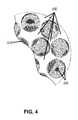
- the temperature profilealso called a thermal profile; see FIG. 4
- the gas streamline pathpasses over both the wafer carrier and wafer regions, and the significant centripetal forces involved during wafer processing.
- the gas streamlinesspiral outward in a generally tangential direction. In one aspect, as shown in FIG.
- exposed portions 400e.g., the area between the wafers
- exposed portions 400are quite hot relative to the other regions of the carrier, as the heat flux streamlines have channeled the streamlines into this region due to the “blanketing” effect.
- the gas pathscreate a tangential gradient in temperature due to the convective cooling, which is hotter at the leading edge (entry of the fluid streamline to the wafer) relative to the trailing edge (exit of the fluid streamline over the wafer). As shown in FIG. 4 , this can result in significant temperature non-uniformities on the surface of the wafer that reduce production yield.
- the center of the wafer surfaceis relatively hotter than other portions of the wafer surface due to the “blanketing” effect, as is the outside portion of the periphery of the wafer that contacts the wafer pocket (subject to centripetal force during rotation), due to the “proximity” effect (region 405 ).
- the inside portion of the periphery of the wafer that is closest to the axis of rotation of the wafer carrieris relatively cooler (region 410 ).
- wafer carriersare constructed to receive a plurality of individual top plates, each of which is sized and shaped to cover a corresponding portion of the top surface of the wafer carrier between the wafer pockets.
- wafer carrier pocket 500comprises base plate 505 and top plate 510 .
- top plate 510 and wafer 515are generally in the same horizontal plane and directly contact each other (e.g., FIGS. 5A, 5C, and 5E ).
- wafer 515is situated to rest on the top surface of tabs 520 located in certain locations along the periphery of each pocket 500 . This arrangement is depicted in FIGS. 5C-5E . Tabs 520 can be included to raise wafer 515 off of pocket floor surface 525 of base plate 505 , thereby permitting some flow of gas around the edges and below the bottom surface of wafer 515 . In related configurations, the distance between base plate 505 and top plate 510 is equal to the distance between base plate 505 and wafer 515 .
- similarly-sized tabs 520can be formed, for example, from extensions of base plate 505 to provide the same or similar spacing between top plate 510 and pocket floor surface 525 of base plate 505 , as that between wafer 515 and pocket floor surface 525 of base plate 505 .
- Embodiments configured as suchgenerally maintain similar heat flux in the wafer carrier body regions not covered by wafers (i.e., beneath the areas in the spaces between the wafers), as those regions covered by wafers (i.e., wafer pockets).
- a ring-shaped stepcan occupy the position of tabs 520 (i.e., in lieu of tabs), such that the entire outer periphery of wafer 515 rests on the ring-step.
- a portion of base plate 505can extend upward and occupy a position around the periphery of wafer 515 , such that top plate 510 is generally in the same horizontal plane as wafer 515 , but may not directly contact wafer 515 .
- the portion of base plate 515 that extends upwardis situated between top plate 510 and wafer 515 .
- the distance between base plate 505 and top plate 510 as well as the distance between base plate 505 and wafer 515can generally be kept equal.
- a wafer carriercan be constructed such that top plate 510 occupies the exposed portions of the wafer carrier (i.e., the areas not occupied by wafers; see FIGS. 4 and 6 ).
- top plate 510can be comprised of the same material as wafer 515 , have the same thickness as wafer 515 , and be the same distance from base plate 505 .
- wafer 515is comprised of sapphire
- top plate 510will also be comprised of sapphire.
- top plate 510will also be comprised of silicon (Si).
- top plate 510will also be 500 microns thick. Additionally, if wafer 515 is 50 microns from base plate 505 , then top plate will also be 50 microns from base plate 505 (see, e.g., FIG. 5E ), or if wafer 515 directly contacts base plate 505 , then top plate will also directly contact base plate 505 (see, e.g., FIGS. 5A and 5B ). With respect to base plate 505 in such embodiments, if wafer 515 and top plate 510 are comprised of silicon or sapphire, for example, base plate 505 can generally be comprised of either solid silicon carbide or silicon carbide-coated graphite.
- the top plateis formed from a ceramic material such as a material selected from among: quartz, solid silicon carbide, aluminum nitride, boron nitride, boron carbide, alumina or another refractory material.
- a ceramic materialsuch as a material selected from among: quartz, solid silicon carbide, aluminum nitride, boron nitride, boron carbide, alumina or another refractory material.
- the selection of ceramic material for the top platecan be made in conjunction with the thickness of the top plate, and geometry of the wafer carrier's bottom plate and pocket geometry to produce a thermal insulating effect that is equivalent to the thermal insulating effect of the wafers situated in their respective pockets, thereby producing a uniform heat blanketing effect over the surface of the wafer carrier in operation.
- a wafer comprising siliconcan be used with a base plate comprising solid silicon carbide or silicon carbide coated graphite, and a top plate comprising silicon carbide or aluminum nitride.
- top plate 510can be constructed from materials that have different thermal properties than wafer 515 . The difference in thermal properties can be based on emissivity, coefficient of thermal expansion (CTE), and/or thermal conductivity.
- top plate 510is constructed and situated to form the peripheral walls of each wafer pocket. These peripheral walls will retain the wafers during processing.
- FIGS. 5B and 5Dillustrate other embodiments, in which the peripheral walls 506 for each wafer pocket are formed by extensions of base plate 505 . This type of structure is illustrated in a perspective view in FIG. 6B .
- top plate or top plates 510occupy the exposed areas of the wafer carrier (i.e., the areas not occupied by wafers), and the peripheral walls 506 of the extensions of base plate 505 will retain wafers 515 during processing. Therefore, in the cross-sectional views of FIGS. 5B and 5D , the peripheral walls 506 of the extensions of base plate 505 are located between wafer 515 and top plate 510 . Exemplary embodiments of such configurations are shown in FIG. 6C , wherein top plate 510 is composed of various segments.
- top plate 600can be comprised of a single piece of material that covers the exposed areas of the wafer carrier but leaves holes 605 for the wafers, as shown in FIG. 6A .
- top plate 600surrounds each wafer, as well as the center and outer periphery of the wafer carrier.
- fastening mechanismscan be used to connect top plate 600 to a base plate.
- top plate 600can be connected to a base plate using wire staples 610 .
- wire staples 610can be comprised of molybdenum, or other suitable metal or alloy.
- the use of staples or other fastening mechanismfacilitates removal of the top plate.
- the top plateis secured to the bottom plate using sintering, a high-temperature adhesive, or other form of permanent bonding.
- top plate 600can be comprised of multiple pieces, each having a shape corresponding to an exposed area of the wafer carrier, as shown in FIG. 6B .
- top plate segments 615can surround the circumference of each wafer, as well as the center and outer periphery of the wafer carrier, but do not physically connect to other top plate segments 615 .
- top plate 600 or top plate segments 615can be comprised of the same material as the wafers, have the same thickness as the wafers, and be the same distance from base plate, in order to reduce temperature non-uniformities.
- the material between the top plate and the wafersis different, while their relative thickness is correspondingly different to produce an equivalent thermal insulating effect.
- a difference between the spacing between the bottom plate and the wafer on the one hand, and the spacing between the bottom plate and the top plate on the other handis compensated by suitable variation in the material, the thickness, or both properties, between the top plate and the wafers, so as to provide a uniform thermal insulation characteristic over the surface of the wafer carrier.
- embodiments of a wafer carriercan comprise a base plate 705 and top plate 710 , such that wafer 715 is not situated to rest on any portion of base plate 705 , including tabs or a ring structure of base plate 705 . Instead, wafer 715 can be situated to rest directly on pocket floor surface 725 of pocket 700 created within top plate 710 , as shown in FIG. 7A . In such configurations, peripheral walls 706 of wafer pocket 700 are provided by top plate 710 . Peripheral walls 706 will retain wafer 715 during processing. In related embodiments, as shown in FIG.
- wafer 715can be situated to rest on the top surface of tabs 720 extending outward from top plate 710 .
- Tabs 720can be located in certain locations along the periphery of each pocket 700 , such that top plate 710 and wafer 715 are generally in the same horizontal plane and directly contact each other.
- Tabs 720raise wafer 715 off pocket floor surface 730 of base plate 705 , thereby permitting some flow of gas around the edges and below the bottom surface of wafer 715 ( FIG. 7B ).
- similarly-sized tabs 720can be formed from extensions of top plate 710 to provide the same or similar spacing between top plate 710 and floor surface 726 of base plate 705 in areas not covered by wafers 715 , as the spacing between pocket floor surface 725 created within top plate 710 in areas covered by wafers 715 ( FIG. 7C ).
- Embodiments configured as suchmaintain similar heat flux in the wafer carrier body regions not covered by wafers (i.e., beneath the areas in the spaces between the wafers), as those regions beneath the wafers (i.e., wafer pockets).
- top plate 700can be comprised of a single piece of material that covers the exposed areas of the wafer carrier but leaves holes for wafers 715 (See FIG. 6A ). In other embodiments, top plate 700 can be comprised of multiple pieces, each having a shape corresponding to an exposed area of the wafer carrier (See FIG. 6B ).
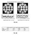
- Tangential temperature gradient profiles obtained during MOCVD processingcan indicate the presence and degree of temperature non-uniformities on the surface of wafers and on the exposed areas of the wafer carrier.
- the tangential temperature gradient profileindicates significant temperature variability on the surface of gallium nitride (GaN) wafers and exposed areas of the wafer carrier (right panels; “standard carrier”).
- GaNgallium nitride
- standard carrierexposed areas of the wafer carrier
- the use of a wafer carrier comprising the top plate and base plate configurations described hereinsignificantly reduces the temperature variability (left panels; “cover carrier”).
- Similar reductions in temperature variabilityare obtained using wafers with multiple quantum wells (MQW), as shown in the tangential temperature gradient profiles in FIG. 9A and the corresponding table summarizing the data in FIG. 9B .
- MQWmultiple quantum wells
- the use of a wafer carriercomprising the top plate and base plate configurations described herein can reduce temperature variability during CVD processing by a factor of about 2.0, 2.5, 3.0, 3.5, 4.0, 4.5, 5.0, 5.5, 6.0, 6.5, 7.0, 7.5, 8.0, 8.5, 9.0, 9.5, or 10.
Landscapes
- Engineering & Computer Science (AREA)
- Chemical & Material Sciences (AREA)
- Manufacturing & Machinery (AREA)
- General Physics & Mathematics (AREA)
- Physics & Mathematics (AREA)
- Computer Hardware Design (AREA)
- Microelectronics & Electronic Packaging (AREA)
- Power Engineering (AREA)
- Condensed Matter Physics & Semiconductors (AREA)
- General Chemical & Material Sciences (AREA)
- Chemical Kinetics & Catalysis (AREA)
- Materials Engineering (AREA)
- Mechanical Engineering (AREA)
- Metallurgy (AREA)
- Organic Chemistry (AREA)
- Chemical Vapour Deposition (AREA)
Abstract
Description
Claims (14)
Priority Applications (2)
| Application Number | Priority Date | Filing Date | Title |
|---|---|---|---|
| US14/583,346US10134617B2 (en) | 2013-12-26 | 2014-12-26 | Wafer carrier having thermal cover for chemical vapor deposition systems |
| US16/191,645US20190157125A1 (en) | 2013-12-26 | 2018-11-15 | Wafer carrier having thermal cover for chemical vapor deposition systems |
Applications Claiming Priority (2)
| Application Number | Priority Date | Filing Date | Title |
|---|---|---|---|
| US201361920943P | 2013-12-26 | 2013-12-26 | |
| US14/583,346US10134617B2 (en) | 2013-12-26 | 2014-12-26 | Wafer carrier having thermal cover for chemical vapor deposition systems |
Related Child Applications (1)
| Application Number | Title | Priority Date | Filing Date |
|---|---|---|---|
| US16/191,645DivisionUS20190157125A1 (en) | 2013-12-26 | 2018-11-15 | Wafer carrier having thermal cover for chemical vapor deposition systems |
Publications (2)
| Publication Number | Publication Date |
|---|---|
| US20150187620A1 US20150187620A1 (en) | 2015-07-02 |
| US10134617B2true US10134617B2 (en) | 2018-11-20 |
Family
ID=53479714
Family Applications (2)
| Application Number | Title | Priority Date | Filing Date |
|---|---|---|---|
| US14/583,346Expired - Fee RelatedUS10134617B2 (en) | 2013-12-26 | 2014-12-26 | Wafer carrier having thermal cover for chemical vapor deposition systems |
| US16/191,645AbandonedUS20190157125A1 (en) | 2013-12-26 | 2018-11-15 | Wafer carrier having thermal cover for chemical vapor deposition systems |
Family Applications After (1)
| Application Number | Title | Priority Date | Filing Date |
|---|---|---|---|
| US16/191,645AbandonedUS20190157125A1 (en) | 2013-12-26 | 2018-11-15 | Wafer carrier having thermal cover for chemical vapor deposition systems |
Country Status (3)
| Country | Link |
|---|---|
| US (2) | US10134617B2 (en) |
| TW (1) | TWI650832B (en) |
| WO (1) | WO2015100437A1 (en) |
Cited By (295)
| Publication number | Priority date | Publication date | Assignee | Title |
|---|---|---|---|---|
| US20170352575A1 (en)* | 2016-06-07 | 2017-12-07 | Applied Materials, Inc. | Contour Pocket And Hybrid Susceptor For Wafer Uniformity |
| US20180350653A1 (en)* | 2017-05-30 | 2018-12-06 | Asm Ip Holding B.V. | Substrate supporting device and substrate processing apparatus including the same |
| US10844484B2 (en) | 2017-09-22 | 2020-11-24 | Asm Ip Holding B.V. | Apparatus for dispensing a vapor phase reactant to a reaction chamber and related methods |
| US10847366B2 (en) | 2018-11-16 | 2020-11-24 | Asm Ip Holding B.V. | Methods for depositing a transition metal chalcogenide film on a substrate by a cyclical deposition process |
| US10844486B2 (en) | 2009-04-06 | 2020-11-24 | Asm Ip Holding B.V. | Semiconductor processing reactor and components thereof |
| US10851456B2 (en) | 2016-04-21 | 2020-12-01 | Asm Ip Holding B.V. | Deposition of metal borides |
| US10858737B2 (en) | 2014-07-28 | 2020-12-08 | Asm Ip Holding B.V. | Showerhead assembly and components thereof |
| US10867788B2 (en) | 2016-12-28 | 2020-12-15 | Asm Ip Holding B.V. | Method of forming a structure on a substrate |
| US10867786B2 (en) | 2018-03-30 | 2020-12-15 | Asm Ip Holding B.V. | Substrate processing method |
| US10883175B2 (en) | 2018-08-09 | 2021-01-05 | Asm Ip Holding B.V. | Vertical furnace for processing substrates and a liner for use therein |
| US10886123B2 (en) | 2017-06-02 | 2021-01-05 | Asm Ip Holding B.V. | Methods for forming low temperature semiconductor layers and related semiconductor device structures |
| US10892156B2 (en) | 2017-05-08 | 2021-01-12 | Asm Ip Holding B.V. | Methods for forming a silicon nitride film on a substrate and related semiconductor device structures |
| US10910262B2 (en) | 2017-11-16 | 2021-02-02 | Asm Ip Holding B.V. | Method of selectively depositing a capping layer structure on a semiconductor device structure |
| US10914004B2 (en) | 2018-06-29 | 2021-02-09 | Asm Ip Holding B.V. | Thin-film deposition method and manufacturing method of semiconductor device |
| US10923344B2 (en) | 2017-10-30 | 2021-02-16 | Asm Ip Holding B.V. | Methods for forming a semiconductor structure and related semiconductor structures |
| US10928731B2 (en) | 2017-09-21 | 2021-02-23 | Asm Ip Holding B.V. | Method of sequential infiltration synthesis treatment of infiltrateable material and structures and devices formed using same |
| US10934619B2 (en) | 2016-11-15 | 2021-03-02 | Asm Ip Holding B.V. | Gas supply unit and substrate processing apparatus including the gas supply unit |
| US10941490B2 (en) | 2014-10-07 | 2021-03-09 | Asm Ip Holding B.V. | Multiple temperature range susceptor, assembly, reactor and system including the susceptor, and methods of using the same |
| US10943771B2 (en) | 2016-10-26 | 2021-03-09 | Asm Ip Holding B.V. | Methods for thermally calibrating reaction chambers |
| US10950432B2 (en) | 2017-04-25 | 2021-03-16 | Asm Ip Holding B.V. | Method of depositing thin film and method of manufacturing semiconductor device |
| USD913980S1 (en) | 2018-02-01 | 2021-03-23 | Asm Ip Holding B.V. | Gas supply plate for semiconductor manufacturing apparatus |
| US10975470B2 (en) | 2018-02-23 | 2021-04-13 | Asm Ip Holding B.V. | Apparatus for detecting or monitoring for a chemical precursor in a high temperature environment |
| US11001925B2 (en) | 2016-12-19 | 2021-05-11 | Asm Ip Holding B.V. | Substrate processing apparatus |
| US11004977B2 (en) | 2017-07-19 | 2021-05-11 | Asm Ip Holding B.V. | Method for depositing a group IV semiconductor and related semiconductor device structures |
| US11015245B2 (en) | 2014-03-19 | 2021-05-25 | Asm Ip Holding B.V. | Gas-phase reactor and system having exhaust plenum and components thereof |
| US11018047B2 (en) | 2018-01-25 | 2021-05-25 | Asm Ip Holding B.V. | Hybrid lift pin |
| US11018002B2 (en) | 2017-07-19 | 2021-05-25 | Asm Ip Holding B.V. | Method for selectively depositing a Group IV semiconductor and related semiconductor device structures |
| US11024523B2 (en) | 2018-09-11 | 2021-06-01 | Asm Ip Holding B.V. | Substrate processing apparatus and method |
| US11022879B2 (en) | 2017-11-24 | 2021-06-01 | Asm Ip Holding B.V. | Method of forming an enhanced unexposed photoresist layer |
| US11031242B2 (en) | 2018-11-07 | 2021-06-08 | Asm Ip Holding B.V. | Methods for depositing a boron doped silicon germanium film |
| USD922229S1 (en) | 2019-06-05 | 2021-06-15 | Asm Ip Holding B.V. | Device for controlling a temperature of a gas supply unit |
| US11049751B2 (en) | 2018-09-14 | 2021-06-29 | Asm Ip Holding B.V. | Cassette supply system to store and handle cassettes and processing apparatus equipped therewith |
| US11056567B2 (en) | 2018-05-11 | 2021-07-06 | Asm Ip Holding B.V. | Method of forming a doped metal carbide film on a substrate and related semiconductor device structures |
| US11053591B2 (en) | 2018-08-06 | 2021-07-06 | Asm Ip Holding B.V. | Multi-port gas injection system and reactor system including same |
| US11056344B2 (en) | 2017-08-30 | 2021-07-06 | Asm Ip Holding B.V. | Layer forming method |
| US11069510B2 (en) | 2017-08-30 | 2021-07-20 | Asm Ip Holding B.V. | Substrate processing apparatus |
| US11081345B2 (en) | 2018-02-06 | 2021-08-03 | Asm Ip Holding B.V. | Method of post-deposition treatment for silicon oxide film |
| US11088002B2 (en) | 2018-03-29 | 2021-08-10 | Asm Ip Holding B.V. | Substrate rack and a substrate processing system and method |
| US11087997B2 (en) | 2018-10-31 | 2021-08-10 | Asm Ip Holding B.V. | Substrate processing apparatus for processing substrates |
| US11094546B2 (en) | 2017-10-05 | 2021-08-17 | Asm Ip Holding B.V. | Method for selectively depositing a metallic film on a substrate |
| US11094582B2 (en) | 2016-07-08 | 2021-08-17 | Asm Ip Holding B.V. | Selective deposition method to form air gaps |
| US11101370B2 (en) | 2016-05-02 | 2021-08-24 | Asm Ip Holding B.V. | Method of forming a germanium oxynitride film |
| US11107676B2 (en) | 2016-07-28 | 2021-08-31 | Asm Ip Holding B.V. | Method and apparatus for filling a gap |
| US11114294B2 (en) | 2019-03-08 | 2021-09-07 | Asm Ip Holding B.V. | Structure including SiOC layer and method of forming same |
| US11114283B2 (en) | 2018-03-16 | 2021-09-07 | Asm Ip Holding B.V. | Reactor, system including the reactor, and methods of manufacturing and using same |
| USD930782S1 (en) | 2019-08-22 | 2021-09-14 | Asm Ip Holding B.V. | Gas distributor |
| US11127617B2 (en) | 2017-11-27 | 2021-09-21 | Asm Ip Holding B.V. | Storage device for storing wafer cassettes for use with a batch furnace |
| US11127589B2 (en) | 2019-02-01 | 2021-09-21 | Asm Ip Holding B.V. | Method of topology-selective film formation of silicon oxide |
| USD931978S1 (en) | 2019-06-27 | 2021-09-28 | Asm Ip Holding B.V. | Showerhead vacuum transport |
| US11139308B2 (en) | 2015-12-29 | 2021-10-05 | Asm Ip Holding B.V. | Atomic layer deposition of III-V compounds to form V-NAND devices |
| US11139191B2 (en) | 2017-08-09 | 2021-10-05 | Asm Ip Holding B.V. | Storage apparatus for storing cassettes for substrates and processing apparatus equipped therewith |
| US11158513B2 (en) | 2018-12-13 | 2021-10-26 | Asm Ip Holding B.V. | Methods for forming a rhenium-containing film on a substrate by a cyclical deposition process and related semiconductor device structures |
| US11164955B2 (en) | 2017-07-18 | 2021-11-02 | Asm Ip Holding B.V. | Methods for forming a semiconductor device structure and related semiconductor device structures |
| USD935572S1 (en) | 2019-05-24 | 2021-11-09 | Asm Ip Holding B.V. | Gas channel plate |
| US11168395B2 (en) | 2018-06-29 | 2021-11-09 | Asm Ip Holding B.V. | Temperature-controlled flange and reactor system including same |
| US11171025B2 (en) | 2019-01-22 | 2021-11-09 | Asm Ip Holding B.V. | Substrate processing device |
| US11205585B2 (en) | 2016-07-28 | 2021-12-21 | Asm Ip Holding B.V. | Substrate processing apparatus and method of operating the same |
| US11217444B2 (en) | 2018-11-30 | 2022-01-04 | Asm Ip Holding B.V. | Method for forming an ultraviolet radiation responsive metal oxide-containing film |
| US11222772B2 (en) | 2016-12-14 | 2022-01-11 | Asm Ip Holding B.V. | Substrate processing apparatus |
| USD940837S1 (en) | 2019-08-22 | 2022-01-11 | Asm Ip Holding B.V. | Electrode |
| US11227782B2 (en) | 2019-07-31 | 2022-01-18 | Asm Ip Holding B.V. | Vertical batch furnace assembly |
| US11227789B2 (en) | 2019-02-20 | 2022-01-18 | Asm Ip Holding B.V. | Method and apparatus for filling a recess formed within a substrate surface |
| US11232963B2 (en) | 2018-10-03 | 2022-01-25 | Asm Ip Holding B.V. | Substrate processing apparatus and method |
| US11233133B2 (en) | 2015-10-21 | 2022-01-25 | Asm Ip Holding B.V. | NbMC layers |
| US11230766B2 (en) | 2018-03-29 | 2022-01-25 | Asm Ip Holding B.V. | Substrate processing apparatus and method |
| US11242598B2 (en) | 2015-06-26 | 2022-02-08 | Asm Ip Holding B.V. | Structures including metal carbide material, devices including the structures, and methods of forming same |
| US11251040B2 (en) | 2019-02-20 | 2022-02-15 | Asm Ip Holding B.V. | Cyclical deposition method including treatment step and apparatus for same |
| US11251068B2 (en) | 2018-10-19 | 2022-02-15 | Asm Ip Holding B.V. | Substrate processing apparatus and substrate processing method |
| US11251035B2 (en) | 2016-12-22 | 2022-02-15 | Asm Ip Holding B.V. | Method of forming a structure on a substrate |
| USD944946S1 (en) | 2019-06-14 | 2022-03-01 | Asm Ip Holding B.V. | Shower plate |
| US11270899B2 (en) | 2018-06-04 | 2022-03-08 | Asm Ip Holding B.V. | Wafer handling chamber with moisture reduction |
| US11274369B2 (en) | 2018-09-11 | 2022-03-15 | Asm Ip Holding B.V. | Thin film deposition method |
| US11282698B2 (en) | 2019-07-19 | 2022-03-22 | Asm Ip Holding B.V. | Method of forming topology-controlled amorphous carbon polymer film |
| US11286562B2 (en) | 2018-06-08 | 2022-03-29 | Asm Ip Holding B.V. | Gas-phase chemical reactor and method of using same |
| US11286558B2 (en) | 2019-08-23 | 2022-03-29 | Asm Ip Holding B.V. | Methods for depositing a molybdenum nitride film on a surface of a substrate by a cyclical deposition process and related semiconductor device structures including a molybdenum nitride film |
| US11289326B2 (en) | 2019-05-07 | 2022-03-29 | Asm Ip Holding B.V. | Method for reforming amorphous carbon polymer film |
| US11295980B2 (en) | 2017-08-30 | 2022-04-05 | Asm Ip Holding B.V. | Methods for depositing a molybdenum metal film over a dielectric surface of a substrate by a cyclical deposition process and related semiconductor device structures |
| US11296189B2 (en) | 2018-06-21 | 2022-04-05 | Asm Ip Holding B.V. | Method for depositing a phosphorus doped silicon arsenide film and related semiconductor device structures |
| USD947913S1 (en) | 2019-05-17 | 2022-04-05 | Asm Ip Holding B.V. | Susceptor shaft |
| USD948463S1 (en) | 2018-10-24 | 2022-04-12 | Asm Ip Holding B.V. | Susceptor for semiconductor substrate supporting apparatus |
| US11306395B2 (en) | 2017-06-28 | 2022-04-19 | Asm Ip Holding B.V. | Methods for depositing a transition metal nitride film on a substrate by atomic layer deposition and related deposition apparatus |
| USD949319S1 (en) | 2019-08-22 | 2022-04-19 | Asm Ip Holding B.V. | Exhaust duct |
| US11315794B2 (en) | 2019-10-21 | 2022-04-26 | Asm Ip Holding B.V. | Apparatus and methods for selectively etching films |
| US11339476B2 (en) | 2019-10-08 | 2022-05-24 | Asm Ip Holding B.V. | Substrate processing device having connection plates, substrate processing method |
| US11342216B2 (en) | 2019-02-20 | 2022-05-24 | Asm Ip Holding B.V. | Cyclical deposition method and apparatus for filling a recess formed within a substrate surface |
| US11345999B2 (en) | 2019-06-06 | 2022-05-31 | Asm Ip Holding B.V. | Method of using a gas-phase reactor system including analyzing exhausted gas |
| US11355338B2 (en) | 2019-05-10 | 2022-06-07 | Asm Ip Holding B.V. | Method of depositing material onto a surface and structure formed according to the method |
| US11361990B2 (en) | 2018-05-28 | 2022-06-14 | Asm Ip Holding B.V. | Substrate processing method and device manufactured by using the same |
| US11374112B2 (en) | 2017-07-19 | 2022-06-28 | Asm Ip Holding B.V. | Method for depositing a group IV semiconductor and related semiconductor device structures |
| US11378337B2 (en) | 2019-03-28 | 2022-07-05 | Asm Ip Holding B.V. | Door opener and substrate processing apparatus provided therewith |
| US11387106B2 (en) | 2018-02-14 | 2022-07-12 | Asm Ip Holding B.V. | Method for depositing a ruthenium-containing film on a substrate by a cyclical deposition process |
| US11387120B2 (en) | 2017-09-28 | 2022-07-12 | Asm Ip Holding B.V. | Chemical dispensing apparatus and methods for dispensing a chemical to a reaction chamber |
| US11390946B2 (en) | 2019-01-17 | 2022-07-19 | Asm Ip Holding B.V. | Methods of forming a transition metal containing film on a substrate by a cyclical deposition process |
| US11390950B2 (en) | 2017-01-10 | 2022-07-19 | Asm Ip Holding B.V. | Reactor system and method to reduce residue buildup during a film deposition process |
| US11390945B2 (en) | 2019-07-03 | 2022-07-19 | Asm Ip Holding B.V. | Temperature control assembly for substrate processing apparatus and method of using same |
| US11393690B2 (en) | 2018-01-19 | 2022-07-19 | Asm Ip Holding B.V. | Deposition method |
| US11398382B2 (en) | 2018-03-27 | 2022-07-26 | Asm Ip Holding B.V. | Method of forming an electrode on a substrate and a semiconductor device structure including an electrode |
| US11401605B2 (en) | 2019-11-26 | 2022-08-02 | Asm Ip Holding B.V. | Substrate processing apparatus |
| US11411088B2 (en) | 2018-11-16 | 2022-08-09 | Asm Ip Holding B.V. | Methods for forming a metal silicate film on a substrate in a reaction chamber and related semiconductor device structures |
| US11410851B2 (en) | 2017-02-15 | 2022-08-09 | Asm Ip Holding B.V. | Methods for forming a metallic film on a substrate by cyclical deposition and related semiconductor device structures |
| US11417545B2 (en) | 2017-08-08 | 2022-08-16 | Asm Ip Holding B.V. | Radiation shield |
| US11414760B2 (en) | 2018-10-08 | 2022-08-16 | Asm Ip Holding B.V. | Substrate support unit, thin film deposition apparatus including the same, and substrate processing apparatus including the same |
| US11424119B2 (en) | 2019-03-08 | 2022-08-23 | Asm Ip Holding B.V. | Method for selective deposition of silicon nitride layer and structure including selectively-deposited silicon nitride layer |
| US11430640B2 (en) | 2019-07-30 | 2022-08-30 | Asm Ip Holding B.V. | Substrate processing apparatus |
| US11430674B2 (en) | 2018-08-22 | 2022-08-30 | Asm Ip Holding B.V. | Sensor array, apparatus for dispensing a vapor phase reactant to a reaction chamber and related methods |
| US11437241B2 (en) | 2020-04-08 | 2022-09-06 | Asm Ip Holding B.V. | Apparatus and methods for selectively etching silicon oxide films |
| US11443926B2 (en) | 2019-07-30 | 2022-09-13 | Asm Ip Holding B.V. | Substrate processing apparatus |
| US11447864B2 (en) | 2019-04-19 | 2022-09-20 | Asm Ip Holding B.V. | Layer forming method and apparatus |
| US11447861B2 (en) | 2016-12-15 | 2022-09-20 | Asm Ip Holding B.V. | Sequential infiltration synthesis apparatus and a method of forming a patterned structure |
| US11447865B2 (en) | 2020-11-17 | 2022-09-20 | Applied Materials, Inc. | Deposition of low-κ films |
| USD965044S1 (en) | 2019-08-19 | 2022-09-27 | Asm Ip Holding B.V. | Susceptor shaft |
| US11453943B2 (en) | 2016-05-25 | 2022-09-27 | Asm Ip Holding B.V. | Method for forming carbon-containing silicon/metal oxide or nitride film by ALD using silicon precursor and hydrocarbon precursor |
| USD965524S1 (en) | 2019-08-19 | 2022-10-04 | Asm Ip Holding B.V. | Susceptor support |
| US11469098B2 (en) | 2018-05-08 | 2022-10-11 | Asm Ip Holding B.V. | Methods for depositing an oxide film on a substrate by a cyclical deposition process and related device structures |
| US11476109B2 (en) | 2019-06-11 | 2022-10-18 | Asm Ip Holding B.V. | Method of forming an electronic structure using reforming gas, system for performing the method, and structure formed using the method |
| US11473195B2 (en) | 2018-03-01 | 2022-10-18 | Asm Ip Holding B.V. | Semiconductor processing apparatus and a method for processing a substrate |
| US11482533B2 (en) | 2019-02-20 | 2022-10-25 | Asm Ip Holding B.V. | Apparatus and methods for plug fill deposition in 3-D NAND applications |
| US11482412B2 (en) | 2018-01-19 | 2022-10-25 | Asm Ip Holding B.V. | Method for depositing a gap-fill layer by plasma-assisted deposition |
| US11482418B2 (en) | 2018-02-20 | 2022-10-25 | Asm Ip Holding B.V. | Substrate processing method and apparatus |
| US11488854B2 (en) | 2020-03-11 | 2022-11-01 | Asm Ip Holding B.V. | Substrate handling device with adjustable joints |
| US11488819B2 (en) | 2018-12-04 | 2022-11-01 | Asm Ip Holding B.V. | Method of cleaning substrate processing apparatus |
| US11492703B2 (en) | 2018-06-27 | 2022-11-08 | Asm Ip Holding B.V. | Cyclic deposition methods for forming metal-containing material and films and structures including the metal-containing material |
| US11495459B2 (en) | 2019-09-04 | 2022-11-08 | Asm Ip Holding B.V. | Methods for selective deposition using a sacrificial capping layer |
| US11501968B2 (en) | 2019-11-15 | 2022-11-15 | Asm Ip Holding B.V. | Method for providing a semiconductor device with silicon filled gaps |
| US11499226B2 (en) | 2018-11-02 | 2022-11-15 | Asm Ip Holding B.V. | Substrate supporting unit and a substrate processing device including the same |
| US11501956B2 (en) | 2012-10-12 | 2022-11-15 | Asm Ip Holding B.V. | Semiconductor reaction chamber showerhead |
| US11501973B2 (en) | 2018-01-16 | 2022-11-15 | Asm Ip Holding B.V. | Method for depositing a material film on a substrate within a reaction chamber by a cyclical deposition process and related device structures |
| US11499222B2 (en) | 2018-06-27 | 2022-11-15 | Asm Ip Holding B.V. | Cyclic deposition methods for forming metal-containing material and films and structures including the metal-containing material |
| US11515188B2 (en) | 2019-05-16 | 2022-11-29 | Asm Ip Holding B.V. | Wafer boat handling device, vertical batch furnace and method |
| US11515187B2 (en) | 2020-05-01 | 2022-11-29 | Asm Ip Holding B.V. | Fast FOUP swapping with a FOUP handler |
| US11521851B2 (en) | 2020-02-03 | 2022-12-06 | Asm Ip Holding B.V. | Method of forming structures including a vanadium or indium layer |
| US11527403B2 (en) | 2019-12-19 | 2022-12-13 | Asm Ip Holding B.V. | Methods for filling a gap feature on a substrate surface and related semiconductor structures |
| US11527400B2 (en) | 2019-08-23 | 2022-12-13 | Asm Ip Holding B.V. | Method for depositing silicon oxide film having improved quality by peald using bis(diethylamino)silane |
| US11532757B2 (en) | 2016-10-27 | 2022-12-20 | Asm Ip Holding B.V. | Deposition of charge trapping layers |
| US11530483B2 (en) | 2018-06-21 | 2022-12-20 | Asm Ip Holding B.V. | Substrate processing system |
| US11530876B2 (en) | 2020-04-24 | 2022-12-20 | Asm Ip Holding B.V. | Vertical batch furnace assembly comprising a cooling gas supply |
| US11551925B2 (en) | 2019-04-01 | 2023-01-10 | Asm Ip Holding B.V. | Method for manufacturing a semiconductor device |
| US11551912B2 (en) | 2020-01-20 | 2023-01-10 | Asm Ip Holding B.V. | Method of forming thin film and method of modifying surface of thin film |
| US11549181B2 (en) | 2013-11-22 | 2023-01-10 | Applied Materials, Inc. | Methods for atomic layer deposition of SiCO(N) using halogenated silylamides |
| USD975665S1 (en) | 2019-05-17 | 2023-01-17 | Asm Ip Holding B.V. | Susceptor shaft |
| US11557474B2 (en) | 2019-07-29 | 2023-01-17 | Asm Ip Holding B.V. | Methods for selective deposition utilizing n-type dopants and/or alternative dopants to achieve high dopant incorporation |
| US11562901B2 (en) | 2019-09-25 | 2023-01-24 | Asm Ip Holding B.V. | Substrate processing method |
| US11572620B2 (en) | 2018-11-06 | 2023-02-07 | Asm Ip Holding B.V. | Methods for selectively depositing an amorphous silicon film on a substrate |
| US11581186B2 (en) | 2016-12-15 | 2023-02-14 | Asm Ip Holding B.V. | Sequential infiltration synthesis apparatus |
| US11587815B2 (en) | 2019-07-31 | 2023-02-21 | Asm Ip Holding B.V. | Vertical batch furnace assembly |
| US11587814B2 (en) | 2019-07-31 | 2023-02-21 | Asm Ip Holding B.V. | Vertical batch furnace assembly |
| US11587821B2 (en) | 2017-08-08 | 2023-02-21 | Asm Ip Holding B.V. | Substrate lift mechanism and reactor including same |
| US11594600B2 (en) | 2019-11-05 | 2023-02-28 | Asm Ip Holding B.V. | Structures with doped semiconductor layers and methods and systems for forming same |
| USD979506S1 (en) | 2019-08-22 | 2023-02-28 | Asm Ip Holding B.V. | Insulator |
| US11594450B2 (en) | 2019-08-22 | 2023-02-28 | Asm Ip Holding B.V. | Method for forming a structure with a hole |
| USD980814S1 (en) | 2021-05-11 | 2023-03-14 | Asm Ip Holding B.V. | Gas distributor for substrate processing apparatus |
| USD980813S1 (en) | 2021-05-11 | 2023-03-14 | Asm Ip Holding B.V. | Gas flow control plate for substrate processing apparatus |
| US11605528B2 (en) | 2019-07-09 | 2023-03-14 | Asm Ip Holding B.V. | Plasma device using coaxial waveguide, and substrate treatment method |
| US11610774B2 (en) | 2019-10-02 | 2023-03-21 | Asm Ip Holding B.V. | Methods for forming a topographically selective silicon oxide film by a cyclical plasma-enhanced deposition process |
| US11610775B2 (en) | 2016-07-28 | 2023-03-21 | Asm Ip Holding B.V. | Method and apparatus for filling a gap |
| USD981973S1 (en) | 2021-05-11 | 2023-03-28 | Asm Ip Holding B.V. | Reactor wall for substrate processing apparatus |
| US11615970B2 (en) | 2019-07-17 | 2023-03-28 | Asm Ip Holding B.V. | Radical assist ignition plasma system and method |
| US11626308B2 (en) | 2020-05-13 | 2023-04-11 | Asm Ip Holding B.V. | Laser alignment fixture for a reactor system |
| US11626316B2 (en) | 2019-11-20 | 2023-04-11 | Asm Ip Holding B.V. | Method of depositing carbon-containing material on a surface of a substrate, structure formed using the method, and system for forming the structure |
| US11629407B2 (en) | 2019-02-22 | 2023-04-18 | Asm Ip Holding B.V. | Substrate processing apparatus and method for processing substrates |
| US11629406B2 (en) | 2018-03-09 | 2023-04-18 | Asm Ip Holding B.V. | Semiconductor processing apparatus comprising one or more pyrometers for measuring a temperature of a substrate during transfer of the substrate |
| US11637014B2 (en) | 2019-10-17 | 2023-04-25 | Asm Ip Holding B.V. | Methods for selective deposition of doped semiconductor material |
| US11637011B2 (en) | 2019-10-16 | 2023-04-25 | Asm Ip Holding B.V. | Method of topology-selective film formation of silicon oxide |
| US11639811B2 (en) | 2017-11-27 | 2023-05-02 | Asm Ip Holding B.V. | Apparatus including a clean mini environment |
| US11639548B2 (en) | 2019-08-21 | 2023-05-02 | Asm Ip Holding B.V. | Film-forming material mixed-gas forming device and film forming device |
| US11644758B2 (en) | 2020-07-17 | 2023-05-09 | Asm Ip Holding B.V. | Structures and methods for use in photolithography |
| US11646205B2 (en) | 2019-10-29 | 2023-05-09 | Asm Ip Holding B.V. | Methods of selectively forming n-type doped material on a surface, systems for selectively forming n-type doped material, and structures formed using same |
| US11643724B2 (en) | 2019-07-18 | 2023-05-09 | Asm Ip Holding B.V. | Method of forming structures using a neutral beam |
| US11646184B2 (en) | 2019-11-29 | 2023-05-09 | Asm Ip Holding B.V. | Substrate processing apparatus |
| US11646204B2 (en) | 2020-06-24 | 2023-05-09 | Asm Ip Holding B.V. | Method for forming a layer provided with silicon |
| US11646197B2 (en) | 2018-07-03 | 2023-05-09 | Asm Ip Holding B.V. | Method for depositing silicon-free carbon-containing film as gap-fill layer by pulse plasma-assisted deposition |
| US11649546B2 (en) | 2016-07-08 | 2023-05-16 | Asm Ip Holding B.V. | Organic reactants for atomic layer deposition |
| US11658030B2 (en) | 2017-03-29 | 2023-05-23 | Asm Ip Holding B.V. | Method for forming doped metal oxide films on a substrate by cyclical deposition and related semiconductor device structures |
| US11658029B2 (en) | 2018-12-14 | 2023-05-23 | Asm Ip Holding B.V. | Method of forming a device structure using selective deposition of gallium nitride and system for same |
| US11658035B2 (en) | 2020-06-30 | 2023-05-23 | Asm Ip Holding B.V. | Substrate processing method |
| US11664199B2 (en) | 2018-10-19 | 2023-05-30 | Asm Ip Holding B.V. | Substrate processing apparatus and substrate processing method |
| US11664245B2 (en) | 2019-07-16 | 2023-05-30 | Asm Ip Holding B.V. | Substrate processing device |
| US11664267B2 (en) | 2019-07-10 | 2023-05-30 | Asm Ip Holding B.V. | Substrate support assembly and substrate processing device including the same |
| US11674220B2 (en) | 2020-07-20 | 2023-06-13 | Asm Ip Holding B.V. | Method for depositing molybdenum layers using an underlayer |
| US11676812B2 (en) | 2016-02-19 | 2023-06-13 | Asm Ip Holding B.V. | Method for forming silicon nitride film selectively on top/bottom portions |
| US11680839B2 (en) | 2019-08-05 | 2023-06-20 | Asm Ip Holding B.V. | Liquid level sensor for a chemical source vessel |
| US11685991B2 (en) | 2018-02-14 | 2023-06-27 | Asm Ip Holding B.V. | Method for depositing a ruthenium-containing film on a substrate by a cyclical deposition process |
| US11688603B2 (en) | 2019-07-17 | 2023-06-27 | Asm Ip Holding B.V. | Methods of forming silicon germanium structures |
| USD990441S1 (en) | 2021-09-07 | 2023-06-27 | Asm Ip Holding B.V. | Gas flow control plate |
| USD990534S1 (en) | 2020-09-11 | 2023-06-27 | Asm Ip Holding B.V. | Weighted lift pin |
| US11705333B2 (en) | 2020-05-21 | 2023-07-18 | Asm Ip Holding B.V. | Structures including multiple carbon layers and methods of forming and using same |
| US11718913B2 (en) | 2018-06-04 | 2023-08-08 | Asm Ip Holding B.V. | Gas distribution system and reactor system including same |
| US11725280B2 (en) | 2020-08-26 | 2023-08-15 | Asm Ip Holding B.V. | Method for forming metal silicon oxide and metal silicon oxynitride layers |
| US11725277B2 (en) | 2011-07-20 | 2023-08-15 | Asm Ip Holding B.V. | Pressure transmitter for a semiconductor processing environment |
| US11735422B2 (en) | 2019-10-10 | 2023-08-22 | Asm Ip Holding B.V. | Method of forming a photoresist underlayer and structure including same |
| US11742198B2 (en) | 2019-03-08 | 2023-08-29 | Asm Ip Holding B.V. | Structure including SiOCN layer and method of forming same |
| US11742189B2 (en) | 2015-03-12 | 2023-08-29 | Asm Ip Holding B.V. | Multi-zone reactor, system including the reactor, and method of using the same |
| US11767589B2 (en) | 2020-05-29 | 2023-09-26 | Asm Ip Holding B.V. | Substrate processing device |
| US11769682B2 (en) | 2017-08-09 | 2023-09-26 | Asm Ip Holding B.V. | Storage apparatus for storing cassettes for substrates and processing apparatus equipped therewith |
| US11776846B2 (en) | 2020-02-07 | 2023-10-03 | Asm Ip Holding B.V. | Methods for depositing gap filling fluids and related systems and devices |
| US11781221B2 (en) | 2019-05-07 | 2023-10-10 | Asm Ip Holding B.V. | Chemical source vessel with dip tube |
| US11781243B2 (en) | 2020-02-17 | 2023-10-10 | Asm Ip Holding B.V. | Method for depositing low temperature phosphorous-doped silicon |
| US11802338B2 (en) | 2017-07-26 | 2023-10-31 | Asm Ip Holding B.V. | Chemical treatment, deposition and/or infiltration apparatus and method for using the same |
| US11804364B2 (en) | 2020-05-19 | 2023-10-31 | Asm Ip Holding B.V. | Substrate processing apparatus |
| US11810788B2 (en) | 2016-11-01 | 2023-11-07 | Asm Ip Holding B.V. | Methods for forming a transition metal niobium nitride film on a substrate by atomic layer deposition and related semiconductor device structures |
| US11814747B2 (en) | 2019-04-24 | 2023-11-14 | Asm Ip Holding B.V. | Gas-phase reactor system-with a reaction chamber, a solid precursor source vessel, a gas distribution system, and a flange assembly |
| US11823876B2 (en) | 2019-09-05 | 2023-11-21 | Asm Ip Holding B.V. | Substrate processing apparatus |
| US11821078B2 (en) | 2020-04-15 | 2023-11-21 | Asm Ip Holding B.V. | Method for forming precoat film and method for forming silicon-containing film |
| US11823866B2 (en) | 2020-04-02 | 2023-11-21 | Asm Ip Holding B.V. | Thin film forming method |
| US11828707B2 (en) | 2020-02-04 | 2023-11-28 | Asm Ip Holding B.V. | Method and apparatus for transmittance measurements of large articles |
| US11827981B2 (en) | 2020-10-14 | 2023-11-28 | Asm Ip Holding B.V. | Method of depositing material on stepped structure |
| US11830730B2 (en) | 2017-08-29 | 2023-11-28 | Asm Ip Holding B.V. | Layer forming method and apparatus |
| US11830738B2 (en) | 2020-04-03 | 2023-11-28 | Asm Ip Holding B.V. | Method for forming barrier layer and method for manufacturing semiconductor device |
| US11840761B2 (en) | 2019-12-04 | 2023-12-12 | Asm Ip Holding B.V. | Substrate processing apparatus |
| US11848200B2 (en) | 2017-05-08 | 2023-12-19 | Asm Ip Holding B.V. | Methods for selectively forming a silicon nitride film on a substrate and related semiconductor device structures |
| US11876356B2 (en) | 2020-03-11 | 2024-01-16 | Asm Ip Holding B.V. | Lockout tagout assembly and system and method of using same |
| US11873557B2 (en) | 2020-10-22 | 2024-01-16 | Asm Ip Holding B.V. | Method of depositing vanadium metal |
| US11887857B2 (en) | 2020-04-24 | 2024-01-30 | Asm Ip Holding B.V. | Methods and systems for depositing a layer comprising vanadium, nitrogen, and a further element |
| USD1012873S1 (en) | 2020-09-24 | 2024-01-30 | Asm Ip Holding B.V. | Electrode for semiconductor processing apparatus |
| US11885013B2 (en) | 2019-12-17 | 2024-01-30 | Asm Ip Holding B.V. | Method of forming vanadium nitride layer and structure including the vanadium nitride layer |
| US11885020B2 (en) | 2020-12-22 | 2024-01-30 | Asm Ip Holding B.V. | Transition metal deposition method |
| US11885023B2 (en) | 2018-10-01 | 2024-01-30 | Asm Ip Holding B.V. | Substrate retaining apparatus, system including the apparatus, and method of using same |
| US11891696B2 (en) | 2020-11-30 | 2024-02-06 | Asm Ip Holding B.V. | Injector configured for arrangement within a reaction chamber of a substrate processing apparatus |
| US11898243B2 (en) | 2020-04-24 | 2024-02-13 | Asm Ip Holding B.V. | Method of forming vanadium nitride-containing layer |
| US11901179B2 (en) | 2020-10-28 | 2024-02-13 | Asm Ip Holding B.V. | Method and device for depositing silicon onto substrates |
| US11915929B2 (en) | 2019-11-26 | 2024-02-27 | Asm Ip Holding B.V. | Methods for selectively forming a target film on a substrate comprising a first dielectric surface and a second metallic surface |
| US11923190B2 (en) | 2018-07-03 | 2024-03-05 | Asm Ip Holding B.V. | Method for depositing silicon-free carbon-containing film as gap-fill layer by pulse plasma-assisted deposition |
| US11923181B2 (en) | 2019-11-29 | 2024-03-05 | Asm Ip Holding B.V. | Substrate processing apparatus for minimizing the effect of a filling gas during substrate processing |
| US11929251B2 (en) | 2019-12-02 | 2024-03-12 | Asm Ip Holding B.V. | Substrate processing apparatus having electrostatic chuck and substrate processing method |
| US11946137B2 (en) | 2020-12-16 | 2024-04-02 | Asm Ip Holding B.V. | Runout and wobble measurement fixtures |
| US11959168B2 (en) | 2020-04-29 | 2024-04-16 | Asm Ip Holding B.V. | Solid source precursor vessel |
| US11961741B2 (en) | 2020-03-12 | 2024-04-16 | Asm Ip Holding B.V. | Method for fabricating layer structure having target topological profile |
| USD1023959S1 (en) | 2021-05-11 | 2024-04-23 | Asm Ip Holding B.V. | Electrode for substrate processing apparatus |
| US11967488B2 (en) | 2013-02-01 | 2024-04-23 | Asm Ip Holding B.V. | Method for treatment of deposition reactor |
| US11976359B2 (en) | 2020-01-06 | 2024-05-07 | Asm Ip Holding B.V. | Gas supply assembly, components thereof, and reactor system including same |
| US11987881B2 (en) | 2020-05-22 | 2024-05-21 | Asm Ip Holding B.V. | Apparatus for depositing thin films using hydrogen peroxide |
| US11986868B2 (en) | 2020-02-28 | 2024-05-21 | Asm Ip Holding B.V. | System dedicated for parts cleaning |
| US11993843B2 (en) | 2017-08-31 | 2024-05-28 | Asm Ip Holding B.V. | Substrate processing apparatus |
| US11993847B2 (en) | 2020-01-08 | 2024-05-28 | Asm Ip Holding B.V. | Injector |
| US11996289B2 (en) | 2020-04-16 | 2024-05-28 | Asm Ip Holding B.V. | Methods of forming structures including silicon germanium and silicon layers, devices formed using the methods, and systems for performing the methods |
| US11996309B2 (en) | 2019-05-16 | 2024-05-28 | Asm Ip Holding B.V. | Wafer boat handling device, vertical batch furnace and method |
| US11996292B2 (en) | 2019-10-25 | 2024-05-28 | Asm Ip Holding B.V. | Methods for filling a gap feature on a substrate surface and related semiconductor structures |
| US12009241B2 (en) | 2019-10-14 | 2024-06-11 | Asm Ip Holding B.V. | Vertical batch furnace assembly with detector to detect cassette |
| US12009224B2 (en) | 2020-09-29 | 2024-06-11 | Asm Ip Holding B.V. | Apparatus and method for etching metal nitrides |
| US12006572B2 (en) | 2019-10-08 | 2024-06-11 | Asm Ip Holding B.V. | Reactor system including a gas distribution assembly for use with activated species and method of using same |
| US12020934B2 (en) | 2020-07-08 | 2024-06-25 | Asm Ip Holding B.V. | Substrate processing method |
| US12025484B2 (en) | 2018-05-08 | 2024-07-02 | Asm Ip Holding B.V. | Thin film forming method |
| US12027365B2 (en) | 2020-11-24 | 2024-07-02 | Asm Ip Holding B.V. | Methods for filling a gap and related systems and devices |
| US12033885B2 (en) | 2020-01-06 | 2024-07-09 | Asm Ip Holding B.V. | Channeled lift pin |
| US12040199B2 (en) | 2018-11-28 | 2024-07-16 | Asm Ip Holding B.V. | Substrate processing apparatus for processing substrates |
| US12040200B2 (en) | 2017-06-20 | 2024-07-16 | Asm Ip Holding B.V. | Semiconductor processing apparatus and methods for calibrating a semiconductor processing apparatus |
| US12040177B2 (en) | 2020-08-18 | 2024-07-16 | Asm Ip Holding B.V. | Methods for forming a laminate film by cyclical plasma-enhanced deposition processes |
| US12051567B2 (en) | 2020-10-07 | 2024-07-30 | Asm Ip Holding B.V. | Gas supply unit and substrate processing apparatus including gas supply unit |
| US12051602B2 (en) | 2020-05-04 | 2024-07-30 | Asm Ip Holding B.V. | Substrate processing system for processing substrates with an electronics module located behind a door in a front wall of the substrate processing system |
| US12057314B2 (en) | 2020-05-15 | 2024-08-06 | Asm Ip Holding B.V. | Methods for silicon germanium uniformity control using multiple precursors |
| US12074022B2 (en) | 2020-08-27 | 2024-08-27 | Asm Ip Holding B.V. | Method and system for forming patterned structures using multiple patterning process |
| US12087586B2 (en) | 2020-04-15 | 2024-09-10 | Asm Ip Holding B.V. | Method of forming chromium nitride layer and structure including the chromium nitride layer |
| US12106944B2 (en) | 2020-06-02 | 2024-10-01 | Asm Ip Holding B.V. | Rotating substrate support |
| US12107005B2 (en) | 2020-10-06 | 2024-10-01 | Asm Ip Holding B.V. | Deposition method and an apparatus for depositing a silicon-containing material |
| US12112940B2 (en) | 2019-07-19 | 2024-10-08 | Asm Ip Holding B.V. | Method of forming topology-controlled amorphous carbon polymer film |
| US12125700B2 (en) | 2020-01-16 | 2024-10-22 | Asm Ip Holding B.V. | Method of forming high aspect ratio features |
| US12131885B2 (en) | 2020-12-22 | 2024-10-29 | Asm Ip Holding B.V. | Plasma treatment device having matching box |
| US12129545B2 (en) | 2020-12-22 | 2024-10-29 | Asm Ip Holding B.V. | Precursor capsule, a vessel and a method |
| US12148609B2 (en) | 2020-09-16 | 2024-11-19 | Asm Ip Holding B.V. | Silicon oxide deposition method |
| US12154824B2 (en) | 2020-08-14 | 2024-11-26 | Asm Ip Holding B.V. | Substrate processing method |
| US12159788B2 (en) | 2020-12-14 | 2024-12-03 | Asm Ip Holding B.V. | Method of forming structures for threshold voltage control |
| US12169361B2 (en) | 2019-07-30 | 2024-12-17 | Asm Ip Holding B.V. | Substrate processing apparatus and method |
| US12173404B2 (en) | 2020-03-17 | 2024-12-24 | Asm Ip Holding B.V. | Method of depositing epitaxial material, structure formed using the method, and system for performing the method |
| US12173402B2 (en) | 2018-02-15 | 2024-12-24 | Asm Ip Holding B.V. | Method of forming a transition metal containing film on a substrate by a cyclical deposition process, a method for supplying a transition metal halide compound to a reaction chamber, and related vapor deposition apparatus |
| US12195852B2 (en) | 2020-11-23 | 2025-01-14 | Asm Ip Holding B.V. | Substrate processing apparatus with an injector |
| US12211742B2 (en) | 2020-09-10 | 2025-01-28 | Asm Ip Holding B.V. | Methods for depositing gap filling fluid |
| US12209308B2 (en) | 2020-11-12 | 2025-01-28 | Asm Ip Holding B.V. | Reactor and related methods |
| US12217954B2 (en) | 2020-08-25 | 2025-02-04 | Asm Ip Holding B.V. | Method of cleaning a surface |
| US12218000B2 (en) | 2020-09-25 | 2025-02-04 | Asm Ip Holding B.V. | Semiconductor processing method |
| US12218269B2 (en) | 2020-02-13 | 2025-02-04 | Asm Ip Holding B.V. | Substrate processing apparatus including light receiving device and calibration method of light receiving device |
| US12217946B2 (en) | 2020-10-15 | 2025-02-04 | Asm Ip Holding B.V. | Method of manufacturing semiconductor device, and substrate treatment apparatus using ether-CAT |
| USD1060598S1 (en) | 2021-12-03 | 2025-02-04 | Asm Ip Holding B.V. | Split showerhead cover |
| US12221357B2 (en) | 2020-04-24 | 2025-02-11 | Asm Ip Holding B.V. | Methods and apparatus for stabilizing vanadium compounds |
| US12230531B2 (en) | 2018-04-09 | 2025-02-18 | Asm Ip Holding B.V. | Substrate supporting apparatus, substrate processing apparatus including the same, and substrate processing method |
| US12243747B2 (en) | 2020-04-24 | 2025-03-04 | Asm Ip Holding B.V. | Methods of forming structures including vanadium boride and vanadium phosphide layers |
| US12240760B2 (en) | 2016-03-18 | 2025-03-04 | Asm Ip Holding B.V. | Aligned carbon nanotubes |
| US12241158B2 (en) | 2020-07-20 | 2025-03-04 | Asm Ip Holding B.V. | Method for forming structures including transition metal layers |
| US12243757B2 (en) | 2020-05-21 | 2025-03-04 | Asm Ip Holding B.V. | Flange and apparatus for processing substrates |
| US12243742B2 (en) | 2020-04-21 | 2025-03-04 | Asm Ip Holding B.V. | Method for processing a substrate |
| US12247286B2 (en) | 2019-08-09 | 2025-03-11 | Asm Ip Holding B.V. | Heater assembly including cooling apparatus and method of using same |
| US12255053B2 (en) | 2020-12-10 | 2025-03-18 | Asm Ip Holding B.V. | Methods and systems for depositing a layer |
| US12252785B2 (en) | 2019-06-10 | 2025-03-18 | Asm Ip Holding B.V. | Method for cleaning quartz epitaxial chambers |
| US12266524B2 (en) | 2020-06-16 | 2025-04-01 | Asm Ip Holding B.V. | Method for depositing boron containing silicon germanium layers |
| US12272527B2 (en) | 2018-05-09 | 2025-04-08 | Asm Ip Holding B.V. | Apparatus for use with hydrogen radicals and method of using same |
| US12276023B2 (en) | 2017-08-04 | 2025-04-15 | Asm Ip Holding B.V. | Showerhead assembly for distributing a gas within a reaction chamber |
| US12278129B2 (en) | 2020-03-04 | 2025-04-15 | Asm Ip Holding B.V. | Alignment fixture for a reactor system |
| US12288710B2 (en) | 2020-12-18 | 2025-04-29 | Asm Ip Holding B.V. | Wafer processing apparatus with a rotatable table |
| US12322591B2 (en) | 2020-07-27 | 2025-06-03 | Asm Ip Holding B.V. | Thin film deposition process |
| US12378665B2 (en) | 2018-10-26 | 2025-08-05 | Asm Ip Holding B.V. | High temperature coatings for a preclean and etch apparatus and related methods |
| US12406846B2 (en) | 2020-05-26 | 2025-09-02 | Asm Ip Holding B.V. | Method for depositing boron and gallium containing silicon germanium layers |
| US12410515B2 (en) | 2020-01-29 | 2025-09-09 | Asm Ip Holding B.V. | Contaminant trap system for a reactor system |
| US12431354B2 (en) | 2020-07-01 | 2025-09-30 | Asm Ip Holding B.V. | Silicon nitride and silicon oxide deposition methods using fluorine inhibitor |
| US12431334B2 (en) | 2020-02-13 | 2025-09-30 | Asm Ip Holding B.V. | Gas distribution assembly |
| US12428726B2 (en) | 2019-10-08 | 2025-09-30 | Asm Ip Holding B.V. | Gas injection system and reactor system including same |
| US12442082B2 (en) | 2021-05-04 | 2025-10-14 | Asm Ip Holding B.V. | Reactor system comprising a tuning circuit |
Families Citing this family (32)
| Publication number | Priority date | Publication date | Assignee | Title |
|---|---|---|---|---|
| TWI650832B (en)* | 2013-12-26 | 2019-02-11 | 維克儀器公司 | Wafer carrier having thermal cover for chemical vapor deposition systems |
| USD793971S1 (en) | 2015-03-27 | 2017-08-08 | Veeco Instruments Inc. | Wafer carrier with a 14-pocket configuration |
| USD793972S1 (en) | 2015-03-27 | 2017-08-08 | Veeco Instruments Inc. | Wafer carrier with a 31-pocket configuration |
| USD778247S1 (en)* | 2015-04-16 | 2017-02-07 | Veeco Instruments Inc. | Wafer carrier with a multi-pocket configuration |
| US20170162411A1 (en)* | 2015-12-03 | 2017-06-08 | Nanya Technology Corporation | Tray |
| CN107435164A (en)* | 2016-05-25 | 2017-12-05 | 上海新昇半导体科技有限公司 | Epitaxial growth equipment |
| DE102016214445A1 (en)* | 2016-08-04 | 2018-02-08 | Meyer Burger (Germany) Ag | Adapter device for substrate carrier |
| LT3422396T (en) | 2017-06-28 | 2021-09-10 | Meyer Burger (Germany) Gmbh | SUBSTRATE TRANSPORTING UNIT, CLEANING UNIT WITH A TRAY ADAPTED TO THE SUBSTRATE HOLDER OF THE ABOVE EQUIPMENT, AND TREATMENT OF THE SUBSTRATE USING THE ABOVE SUBSTRATE TRANSPORTING DEVICE AND THE CLEANING DEVICE |
| USD860146S1 (en)* | 2017-11-30 | 2019-09-17 | Veeco Instruments Inc. | Wafer carrier with a 33-pocket configuration |
| USD858469S1 (en) | 2018-03-26 | 2019-09-03 | Veeco Instruments Inc. | Chemical vapor deposition wafer carrier with thermal cover |
| USD854506S1 (en) | 2018-03-26 | 2019-07-23 | Veeco Instruments Inc. | Chemical vapor deposition wafer carrier with thermal cover |
| USD866491S1 (en) | 2018-03-26 | 2019-11-12 | Veeco Instruments Inc. | Chemical vapor deposition wafer carrier with thermal cover |
| US20190295880A1 (en)* | 2018-03-26 | 2019-09-26 | Veeco Instruments Inc. | Chemical vapor deposition wafer carrier with thermal cover |
| USD860147S1 (en) | 2018-03-26 | 2019-09-17 | Veeco Instruments Inc. | Chemical vapor deposition wafer carrier with thermal cover |
| USD863239S1 (en) | 2018-03-26 | 2019-10-15 | Veeco Instruments Inc. | Chemical vapor deposition wafer carrier with thermal cover |
| KR102535194B1 (en)* | 2018-04-03 | 2023-05-22 | 주성엔지니어링(주) | Apparatus for Processing Substrate |
| DE102018113400A1 (en) | 2018-06-06 | 2019-12-12 | Aixtron Se | CVD reactor with support ring for substrate handling |
| DE102018114208A1 (en)* | 2018-06-14 | 2019-12-19 | Aixtron Se | Cover plate for covering the side of a susceptor of a device for depositing SiC layers facing the process chamber |
| DE102019114249A1 (en)* | 2018-06-19 | 2019-12-19 | Aixtron Se | Arrangement for measuring the surface temperature of a susceptor in a CVD reactor |
| CN111048464A (en)* | 2018-10-15 | 2020-04-21 | 君泰创新(北京)科技有限公司 | Battery silicon wafer bearing mechanism and transportation equipment |
| US20200255941A1 (en)* | 2019-02-11 | 2020-08-13 | Kennametal Inc. | Supports for chemical vapor deposition coating applications |
| KR102724013B1 (en)* | 2019-11-11 | 2024-10-30 | 주성엔지니어링(주) | Apparatus for Processing Substrate |
| KR20250033324A (en) | 2020-02-11 | 2025-03-07 | 램 리써치 코포레이션 | Carrier ring designs for controlling deposition on wafer bevel/edge |
| CN113201727B (en)* | 2021-04-28 | 2023-02-28 | 錼创显示科技股份有限公司 | Semiconductor wafer carrying structure and metalorganic chemical vapor deposition device |
| US20230060609A1 (en)* | 2021-08-31 | 2023-03-02 | Veeco Instruments Inc. | Wafer carrier assembly with pedestal and cover restraint arrangements that control thermal gaps |
| CN114164414B (en)* | 2021-12-17 | 2022-08-23 | 北京沁圆半导体设备有限公司 | Reaction chamber of chemical vapor deposition device and chemical vapor deposition device |
| CN114464553A (en)* | 2021-12-24 | 2022-05-10 | 徐州鑫晶半导体科技有限公司 | Bearing platform for wafer annealing |
| KR20250008782A (en)* | 2022-05-13 | 2025-01-15 | 램 리써치 코포레이션 | Carrier ring with tab |
| TW202414658A (en)* | 2022-09-23 | 2024-04-01 | 美商維克儀器公司 | Wafer carrier assembly with improved temperature uniformity |
| KR20250117369A (en)* | 2022-11-28 | 2025-08-04 | 비코 인스트루먼츠 인코포레이티드 | Multi-disk chemical vapor deposition system using cross-flow gas injection |
| CN115928041A (en)* | 2022-12-12 | 2023-04-07 | 中山德华芯片技术有限公司 | A graphite disk structure |
| NL2033744B1 (en)* | 2022-12-16 | 2024-06-20 | Applied Nanolayers B V | Substrate retainer |
Citations (56)
| Publication number | Priority date | Publication date | Assignee | Title |
|---|---|---|---|---|
| US3895967A (en) | 1973-10-30 | 1975-07-22 | Gen Electric | Semiconductor device production |
| JPS58128724A (en) | 1982-01-27 | 1983-08-01 | Hitachi Ltd | Wafer reversal device |
| JPH04110466A (en) | 1990-08-31 | 1992-04-10 | Oki Electric Ind Co Ltd | Wafer holder |
| US5152842A (en) | 1991-12-05 | 1992-10-06 | Rohm Co., Ltd. | Reactor for epitaxial growth |
| US5242501A (en) | 1982-09-10 | 1993-09-07 | Lam Research Corporation | Susceptor in chemical vapor deposition reactors |
| EP0795624A1 (en) | 1996-03-15 | 1997-09-17 | STMicroelectronics S.A. | Substrate holder for evaporation apparatus |
| US5690742A (en) | 1994-09-06 | 1997-11-25 | Komatsu Electronic Metals Co., Ltd. | Susceptor for an epitaxial growth apparatus |
| JPH10167885A (en) | 1996-12-13 | 1998-06-23 | Toyo Tanso Kk | Susceptor for vapor growth |
| JPH10167886A (en) | 1996-12-13 | 1998-06-23 | Toyo Tanso Kk | Susceptor for vapor growth |
| WO1999018599A2 (en) | 1997-10-03 | 1999-04-15 | Koninklijke Philips Electronics N.V. | Holder for a semiconductor substrate, and method of manufacturing a semiconductor device using such a holder |
| US6001183A (en) | 1996-06-10 | 1999-12-14 | Emcore Corporation | Wafer carriers for epitaxial growth processes |
| EP1096549A2 (en) | 1999-10-29 | 2001-05-02 | The Boc Group, Inc. | Substrates support devices |
| US6436796B1 (en) | 2000-01-31 | 2002-08-20 | Mattson Technology, Inc. | Systems and methods for epitaxial processing of a semiconductor substrate |
| US6492625B1 (en) | 2000-09-27 | 2002-12-10 | Emcore Corporation | Apparatus and method for controlling temperature uniformity of substrates |
| US6506252B2 (en) | 2001-02-07 | 2003-01-14 | Emcore Corporation | Susceptorless reactor for growing epitaxial layers on wafers by chemical vapor deposition |
| WO2003069029A1 (en) | 2002-02-15 | 2003-08-21 | Lpe Spa | A susceptor provided with indentations and an epitaxial reactor which uses the same |
| US6666756B1 (en) | 2000-03-31 | 2003-12-23 | Lam Research Corporation | Wafer carrier head assembly |
| JP2004128271A (en) | 2002-10-03 | 2004-04-22 | Toyo Tanso Kk | Susceptor |
| US20050011436A1 (en) | 2003-07-15 | 2005-01-20 | Heng Liu | Chemical vapor deposition reactor |
| US6902623B2 (en) | 2001-06-07 | 2005-06-07 | Veeco Instruments Inc. | Reactor having a movable shutter |
| US20050274374A1 (en)* | 2004-06-09 | 2005-12-15 | Veeco Instruments Inc. | System and method for increasing the emissivity of a material |
| JP2006066417A (en) | 2004-08-24 | 2006-03-09 | Ulvac Japan Ltd | Electrostatic chuck and substrate transfer tray |
| US7101272B2 (en) | 2005-01-15 | 2006-09-05 | Applied Materials, Inc. | Carrier head for thermal drift compensation |
| US7122844B2 (en) | 2002-05-13 | 2006-10-17 | Cree, Inc. | Susceptor for MOCVD reactor |
| US20070186853A1 (en) | 2006-02-10 | 2007-08-16 | Veeco Instruments Inc. | System and method for varying wafer surface temperature via wafer-carrier temperature offset |
| DE10261362B4 (en) | 2002-12-30 | 2008-05-21 | Osram Opto Semiconductors Gmbh | Substrate holder |
| JP4110466B2 (en) | 2002-09-11 | 2008-07-02 | 東洋紡績株式会社 | High density fabric for airbags |
| KR100854974B1 (en) | 2007-04-25 | 2008-08-28 | (주)리드 | Substrate carrier and apparatus for manufacturing light emitting diode using same |
| KR20090036722A (en) | 2007-10-10 | 2009-04-15 | 주성엔지니어링(주) | Substrate support and thin film deposition apparatus having the same |
| KR20090038606A (en) | 2007-10-16 | 2009-04-21 | 엘지이노텍 주식회사 | Susceptor and semiconductor manufacturing method using same |
| US20090155028A1 (en) | 2007-12-12 | 2009-06-18 | Veeco Instruments Inc. | Wafer carrier with hub |
| US20100055320A1 (en) | 2008-09-04 | 2010-03-04 | Tokyo Electron Limited | Film deposition apparatus, substrate processing apparatus, film deposition method and storage medium |
| US20100055318A1 (en) | 2008-08-29 | 2010-03-04 | Veeco Instruments Inc. | Wafer carrier with varying thermal resistance |
| US20110049779A1 (en) | 2009-08-28 | 2011-03-03 | Applied Materials, Inc. | Substrate carrier design for improved photoluminescence uniformity |
| US20110290175A1 (en)* | 2009-06-07 | 2011-12-01 | Veeco Instruments, Inc. | Multi-Chamber CVD Processing System |
| US20110300297A1 (en) | 2010-06-07 | 2011-12-08 | Veeco Instruments Inc. | Multi-wafer rotating disc reactor with inertial planetary drive |
| US8092599B2 (en) | 2007-07-10 | 2012-01-10 | Veeco Instruments Inc. | Movable injectors in rotating disc gas reactors |
| US8093696B2 (en) | 2008-05-16 | 2012-01-10 | Qimonda Ag | Semiconductor device |
| US20120040097A1 (en) | 2010-08-13 | 2012-02-16 | Veeco Instruments Inc. | Enhanced wafer carrier |
| US20120156374A1 (en)* | 2010-12-15 | 2012-06-21 | Veeco Instruments Inc. | Sectional wafer carrier |
| US20120234229A1 (en) | 2011-03-16 | 2012-09-20 | Applied Materials, Inc. | Substrate support assembly for thin film deposition systems |
| US20120272892A1 (en) | 2011-04-07 | 2012-11-01 | Veeco Instruments Inc. | Metal-Organic Vapor Phase Epitaxy System and Process |
| US8367477B2 (en) | 2009-03-13 | 2013-02-05 | Wen-Cheng Chien | Electronic device package and method for forming the same |
| US8366830B2 (en) | 2003-03-04 | 2013-02-05 | Cree, Inc. | Susceptor apparatus for inverted type MOCVD reactor |
| US20130175005A1 (en) | 2012-01-06 | 2013-07-11 | Keerthi Gowdaru | Adaptive heat transfer methods and systems for uniform heat transfer |
| US8486726B2 (en) | 2009-12-02 | 2013-07-16 | Veeco Instruments Inc. | Method for improving performance of a substrate carrier |
| US8518753B2 (en) | 2011-11-15 | 2013-08-27 | Taiwan Semiconductor Manufacturing Company, Ltd. | Assembly method for three dimensional integrated circuit |
| WO2013123859A1 (en) | 2012-02-22 | 2013-08-29 | 光达光电设备科技(嘉兴)有限公司 | Graphite plate, reaction chamber having same, and method for heating substrate |
| US20130291798A1 (en) | 2011-01-14 | 2013-11-07 | Wonik Ip Co., Ltd. | Thin film deposition apparatus and substrate treatment system including the same |
| US20140110894A1 (en) | 2012-10-22 | 2014-04-24 | Samsung Electronics Co., Ltd. | Wafer Carrier Having Cavity |
| US20140261187A1 (en) | 2013-03-15 | 2014-09-18 | Veeco Instruments, Inc. | Wafer carrier having provisions for improving heating uniformity in chemical vapor deposition systems |
| US20140261698A1 (en)* | 2013-03-14 | 2014-09-18 | Veeco Instruments Inc. | Wafer carrier with temperature distribution control |
| US20140360430A1 (en)* | 2013-06-05 | 2014-12-11 | Veeco Instruments, Inc. | Wafer carrier having thermal uniformity-enhancing features |
| US9017483B2 (en) | 2008-03-21 | 2015-04-28 | Sumco Corporation | Susceptor for vapor phase epitaxial growth device |
| US20150187620A1 (en)* | 2013-12-26 | 2015-07-02 | Veeco Instruments Inc. | Water Carrier Having Thermal Cover for Chemical Vapor Deposition Systems |
| US20160251758A1 (en)* | 2010-12-30 | 2016-09-01 | Veeco Instruments Inc. | Wafer processing with carrier extension |
- 2014
- 2014-12-25TWTW103145394Apatent/TWI650832B/ennot_activeIP Right Cessation
- 2014-12-26USUS14/583,346patent/US10134617B2/ennot_activeExpired - Fee Related
- 2014-12-26WOPCT/US2014/072425patent/WO2015100437A1/enactiveApplication Filing
- 2018
- 2018-11-15USUS16/191,645patent/US20190157125A1/ennot_activeAbandoned
Patent Citations (66)
| Publication number | Priority date | Publication date | Assignee | Title |
|---|---|---|---|---|
| US3895967A (en) | 1973-10-30 | 1975-07-22 | Gen Electric | Semiconductor device production |
| JPS58128724A (en) | 1982-01-27 | 1983-08-01 | Hitachi Ltd | Wafer reversal device |
| US5242501A (en) | 1982-09-10 | 1993-09-07 | Lam Research Corporation | Susceptor in chemical vapor deposition reactors |
| JPH04110466A (en) | 1990-08-31 | 1992-04-10 | Oki Electric Ind Co Ltd | Wafer holder |
| US5152842A (en) | 1991-12-05 | 1992-10-06 | Rohm Co., Ltd. | Reactor for epitaxial growth |
| US5690742A (en) | 1994-09-06 | 1997-11-25 | Komatsu Electronic Metals Co., Ltd. | Susceptor for an epitaxial growth apparatus |
| EP0795624A1 (en) | 1996-03-15 | 1997-09-17 | STMicroelectronics S.A. | Substrate holder for evaporation apparatus |
| US6001183A (en) | 1996-06-10 | 1999-12-14 | Emcore Corporation | Wafer carriers for epitaxial growth processes |
| JPH10167885A (en) | 1996-12-13 | 1998-06-23 | Toyo Tanso Kk | Susceptor for vapor growth |
| JPH10167886A (en) | 1996-12-13 | 1998-06-23 | Toyo Tanso Kk | Susceptor for vapor growth |
| WO1999018599A2 (en) | 1997-10-03 | 1999-04-15 | Koninklijke Philips Electronics N.V. | Holder for a semiconductor substrate, and method of manufacturing a semiconductor device using such a holder |
| EP1096549A2 (en) | 1999-10-29 | 2001-05-02 | The Boc Group, Inc. | Substrates support devices |
| US6436796B1 (en) | 2000-01-31 | 2002-08-20 | Mattson Technology, Inc. | Systems and methods for epitaxial processing of a semiconductor substrate |
| US6666756B1 (en) | 2000-03-31 | 2003-12-23 | Lam Research Corporation | Wafer carrier head assembly |
| US6492625B1 (en) | 2000-09-27 | 2002-12-10 | Emcore Corporation | Apparatus and method for controlling temperature uniformity of substrates |
| US6506252B2 (en) | 2001-02-07 | 2003-01-14 | Emcore Corporation | Susceptorless reactor for growing epitaxial layers on wafers by chemical vapor deposition |
| US7276124B2 (en) | 2001-06-07 | 2007-10-02 | Veeco Instruments Inc. | Reactor having a movable shutter |
| US6902623B2 (en) | 2001-06-07 | 2005-06-07 | Veeco Instruments Inc. | Reactor having a movable shutter |
| WO2003069029A1 (en) | 2002-02-15 | 2003-08-21 | Lpe Spa | A susceptor provided with indentations and an epitaxial reactor which uses the same |
| US7122844B2 (en) | 2002-05-13 | 2006-10-17 | Cree, Inc. | Susceptor for MOCVD reactor |
| US8372204B2 (en) | 2002-05-13 | 2013-02-12 | Cree, Inc. | Susceptor for MOCVD reactor |
| JP4110466B2 (en) | 2002-09-11 | 2008-07-02 | 東洋紡績株式会社 | High density fabric for airbags |
| JP2004128271A (en) | 2002-10-03 | 2004-04-22 | Toyo Tanso Kk | Susceptor |
| DE10261362B4 (en) | 2002-12-30 | 2008-05-21 | Osram Opto Semiconductors Gmbh | Substrate holder |
| US8366830B2 (en) | 2003-03-04 | 2013-02-05 | Cree, Inc. | Susceptor apparatus for inverted type MOCVD reactor |
| US20050011436A1 (en) | 2003-07-15 | 2005-01-20 | Heng Liu | Chemical vapor deposition reactor |
| US20050274374A1 (en)* | 2004-06-09 | 2005-12-15 | Veeco Instruments Inc. | System and method for increasing the emissivity of a material |
| JP2006066417A (en) | 2004-08-24 | 2006-03-09 | Ulvac Japan Ltd | Electrostatic chuck and substrate transfer tray |
| US7101272B2 (en) | 2005-01-15 | 2006-09-05 | Applied Materials, Inc. | Carrier head for thermal drift compensation |
| JP5156240B2 (en) | 2006-02-10 | 2013-03-06 | ビーコ・インストゥルメンツ・インコーポレイテッド | System and method for changing surface temperature of wafer by temperature compensation of wafer carrier |
| US8603248B2 (en) | 2006-02-10 | 2013-12-10 | Veeco Instruments Inc. | System and method for varying wafer surface temperature via wafer-carrier temperature offset |
| US20070186853A1 (en) | 2006-02-10 | 2007-08-16 | Veeco Instruments Inc. | System and method for varying wafer surface temperature via wafer-carrier temperature offset |
| KR100854974B1 (en) | 2007-04-25 | 2008-08-28 | (주)리드 | Substrate carrier and apparatus for manufacturing light emitting diode using same |
| US8092599B2 (en) | 2007-07-10 | 2012-01-10 | Veeco Instruments Inc. | Movable injectors in rotating disc gas reactors |
| KR20090036722A (en) | 2007-10-10 | 2009-04-15 | 주성엔지니어링(주) | Substrate support and thin film deposition apparatus having the same |
| KR20090038606A (en) | 2007-10-16 | 2009-04-21 | 엘지이노텍 주식회사 | Susceptor and semiconductor manufacturing method using same |
| US8021487B2 (en) | 2007-12-12 | 2011-09-20 | Veeco Instruments Inc. | Wafer carrier with hub |
| US20090155028A1 (en) | 2007-12-12 | 2009-06-18 | Veeco Instruments Inc. | Wafer carrier with hub |
| US9017483B2 (en) | 2008-03-21 | 2015-04-28 | Sumco Corporation | Susceptor for vapor phase epitaxial growth device |
| US8093696B2 (en) | 2008-05-16 | 2012-01-10 | Qimonda Ag | Semiconductor device |
| US20100055318A1 (en) | 2008-08-29 | 2010-03-04 | Veeco Instruments Inc. | Wafer carrier with varying thermal resistance |
| US20100055320A1 (en) | 2008-09-04 | 2010-03-04 | Tokyo Electron Limited | Film deposition apparatus, substrate processing apparatus, film deposition method and storage medium |
| US8367477B2 (en) | 2009-03-13 | 2013-02-05 | Wen-Cheng Chien | Electronic device package and method for forming the same |
| US8552547B2 (en) | 2009-03-13 | 2013-10-08 | Xintec Inc. | Electronic device package and method for forming the same |
| US20110290175A1 (en)* | 2009-06-07 | 2011-12-01 | Veeco Instruments, Inc. | Multi-Chamber CVD Processing System |
| US20110049779A1 (en) | 2009-08-28 | 2011-03-03 | Applied Materials, Inc. | Substrate carrier design for improved photoluminescence uniformity |
| US8486726B2 (en) | 2009-12-02 | 2013-07-16 | Veeco Instruments Inc. | Method for improving performance of a substrate carrier |
| US20110300297A1 (en) | 2010-06-07 | 2011-12-08 | Veeco Instruments Inc. | Multi-wafer rotating disc reactor with inertial planetary drive |
| US20120040097A1 (en) | 2010-08-13 | 2012-02-16 | Veeco Instruments Inc. | Enhanced wafer carrier |
| US8535445B2 (en) | 2010-08-13 | 2013-09-17 | Veeco Instruments Inc. | Enhanced wafer carrier |
| WO2012021370A1 (en) | 2010-08-13 | 2012-02-16 | Veeco Instruments Inc. | Enhanced wafer carrier |
| US20120156374A1 (en)* | 2010-12-15 | 2012-06-21 | Veeco Instruments Inc. | Sectional wafer carrier |
| US8562746B2 (en) | 2010-12-15 | 2013-10-22 | Veeco Instruments Inc. | Sectional wafer carrier |
| US20160251758A1 (en)* | 2010-12-30 | 2016-09-01 | Veeco Instruments Inc. | Wafer processing with carrier extension |
| US20130291798A1 (en) | 2011-01-14 | 2013-11-07 | Wonik Ip Co., Ltd. | Thin film deposition apparatus and substrate treatment system including the same |
| US20120234229A1 (en) | 2011-03-16 | 2012-09-20 | Applied Materials, Inc. | Substrate support assembly for thin film deposition systems |
| US20120272892A1 (en) | 2011-04-07 | 2012-11-01 | Veeco Instruments Inc. | Metal-Organic Vapor Phase Epitaxy System and Process |
| US8518753B2 (en) | 2011-11-15 | 2013-08-27 | Taiwan Semiconductor Manufacturing Company, Ltd. | Assembly method for three dimensional integrated circuit |
| US20130175005A1 (en) | 2012-01-06 | 2013-07-11 | Keerthi Gowdaru | Adaptive heat transfer methods and systems for uniform heat transfer |
| WO2013123859A1 (en) | 2012-02-22 | 2013-08-29 | 光达光电设备科技(嘉兴)有限公司 | Graphite plate, reaction chamber having same, and method for heating substrate |
| US20140110894A1 (en) | 2012-10-22 | 2014-04-24 | Samsung Electronics Co., Ltd. | Wafer Carrier Having Cavity |
| US20140261698A1 (en)* | 2013-03-14 | 2014-09-18 | Veeco Instruments Inc. | Wafer carrier with temperature distribution control |
| US20140261187A1 (en) | 2013-03-15 | 2014-09-18 | Veeco Instruments, Inc. | Wafer carrier having provisions for improving heating uniformity in chemical vapor deposition systems |
| US20140360430A1 (en)* | 2013-06-05 | 2014-12-11 | Veeco Instruments, Inc. | Wafer carrier having thermal uniformity-enhancing features |
| US20170121847A1 (en)* | 2013-06-05 | 2017-05-04 | Veeco Instruments Inc. | Wafer carrier having thermal uniformity-enhancing features |
| US20150187620A1 (en)* | 2013-12-26 | 2015-07-02 | Veeco Instruments Inc. | Water Carrier Having Thermal Cover for Chemical Vapor Deposition Systems |
Non-Patent Citations (10)
| Title |
|---|
| Application and file history for related U.S. Appl. No. 14/297,244, filed Jun. 5, 2014, Inventors Armour et al. |
| Application and file history for U.S. Appl. No. 15/403,709, filed Jan. 11, 2017. Inventors: Armour et al. |
| Application No. PCT/US2014/072425, filed Dec. 26, 2014, International Search Report dated Apr. 29, 2015, 3 pages. |
| Application No. PCT/US2014/072425, filed Dec. 26, 2014, Written Opinion dated Apr. 29, 2015, 7 pages. |
| Guary et al. "Investigation of the Wafer Temperature Uniformity in an OMVPE Vertical Rotating Disk Reactor", Journal of Electronic Material, Nov. 1995, vol. 24, Issue 11, Abstract, 1 pg. |
| International Search Report and Written Opinion for International Application No. PCT/US2011061615 dated May 18, 2012. |
| International Search Report and Written Opinion from PCT Application PCT/US2014/041134, dated Oct. 7, 2014, 11 pgs. |
| International Search Report from PCT Application PCT/US2011/0456567, dated Dec. 21, 2011, 6 pgs. |
| Machine Generated English Translation of KR100854974.Published Aug. 28, 2008.* |
| Taiwan Application No. 103145394, Search Report dated Jan. 9, 2018, 9 page. |
Cited By (357)
| Publication number | Priority date | Publication date | Assignee | Title |
|---|---|---|---|---|
| US10844486B2 (en) | 2009-04-06 | 2020-11-24 | Asm Ip Holding B.V. | Semiconductor processing reactor and components thereof |
| US11725277B2 (en) | 2011-07-20 | 2023-08-15 | Asm Ip Holding B.V. | Pressure transmitter for a semiconductor processing environment |
| US11501956B2 (en) | 2012-10-12 | 2022-11-15 | Asm Ip Holding B.V. | Semiconductor reaction chamber showerhead |
| US11967488B2 (en) | 2013-02-01 | 2024-04-23 | Asm Ip Holding B.V. | Method for treatment of deposition reactor |
| US11549181B2 (en) | 2013-11-22 | 2023-01-10 | Applied Materials, Inc. | Methods for atomic layer deposition of SiCO(N) using halogenated silylamides |
| US11015245B2 (en) | 2014-03-19 | 2021-05-25 | Asm Ip Holding B.V. | Gas-phase reactor and system having exhaust plenum and components thereof |
| US10858737B2 (en) | 2014-07-28 | 2020-12-08 | Asm Ip Holding B.V. | Showerhead assembly and components thereof |
| US10941490B2 (en) | 2014-10-07 | 2021-03-09 | Asm Ip Holding B.V. | Multiple temperature range susceptor, assembly, reactor and system including the susceptor, and methods of using the same |
| US11795545B2 (en) | 2014-10-07 | 2023-10-24 | Asm Ip Holding B.V. | Multiple temperature range susceptor, assembly, reactor and system including the susceptor, and methods of using the same |
| US11742189B2 (en) | 2015-03-12 | 2023-08-29 | Asm Ip Holding B.V. | Multi-zone reactor, system including the reactor, and method of using the same |
| US11242598B2 (en) | 2015-06-26 | 2022-02-08 | Asm Ip Holding B.V. | Structures including metal carbide material, devices including the structures, and methods of forming same |
| US11233133B2 (en) | 2015-10-21 | 2022-01-25 | Asm Ip Holding B.V. | NbMC layers |
| US11139308B2 (en) | 2015-12-29 | 2021-10-05 | Asm Ip Holding B.V. | Atomic layer deposition of III-V compounds to form V-NAND devices |
| US11956977B2 (en) | 2015-12-29 | 2024-04-09 | Asm Ip Holding B.V. | Atomic layer deposition of III-V compounds to form V-NAND devices |
| US11676812B2 (en) | 2016-02-19 | 2023-06-13 | Asm Ip Holding B.V. | Method for forming silicon nitride film selectively on top/bottom portions |
| US12240760B2 (en) | 2016-03-18 | 2025-03-04 | Asm Ip Holding B.V. | Aligned carbon nanotubes |
| US10851456B2 (en) | 2016-04-21 | 2020-12-01 | Asm Ip Holding B.V. | Deposition of metal borides |
| US11101370B2 (en) | 2016-05-02 | 2021-08-24 | Asm Ip Holding B.V. | Method of forming a germanium oxynitride film |
| US11453943B2 (en) | 2016-05-25 | 2022-09-27 | Asm Ip Holding B.V. | Method for forming carbon-containing silicon/metal oxide or nitride film by ALD using silicon precursor and hydrocarbon precursor |
| US11557501B2 (en) | 2016-06-07 | 2023-01-17 | Applied Materials, Inc. | Contour pocket and hybrid susceptor for wafer uniformity |
| US11810810B2 (en) | 2016-06-07 | 2023-11-07 | Applied Materials, Inc. | Contour pocket and hybrid susceptor for wafer uniformity |
| US10685864B2 (en)* | 2016-06-07 | 2020-06-16 | Applied Materials, Inc. | Contour pocket and hybrid susceptor for wafer uniformity |
| US20170352575A1 (en)* | 2016-06-07 | 2017-12-07 | Applied Materials, Inc. | Contour Pocket And Hybrid Susceptor For Wafer Uniformity |
| US11649546B2 (en) | 2016-07-08 | 2023-05-16 | Asm Ip Holding B.V. | Organic reactants for atomic layer deposition |
| US11094582B2 (en) | 2016-07-08 | 2021-08-17 | Asm Ip Holding B.V. | Selective deposition method to form air gaps |
| US11749562B2 (en) | 2016-07-08 | 2023-09-05 | Asm Ip Holding B.V. | Selective deposition method to form air gaps |
| US11205585B2 (en) | 2016-07-28 | 2021-12-21 | Asm Ip Holding B.V. | Substrate processing apparatus and method of operating the same |
| US11610775B2 (en) | 2016-07-28 | 2023-03-21 | Asm Ip Holding B.V. | Method and apparatus for filling a gap |
| US11107676B2 (en) | 2016-07-28 | 2021-08-31 | Asm Ip Holding B.V. | Method and apparatus for filling a gap |
| US11694892B2 (en) | 2016-07-28 | 2023-07-04 | Asm Ip Holding B.V. | Method and apparatus for filling a gap |
| US10943771B2 (en) | 2016-10-26 | 2021-03-09 | Asm Ip Holding B.V. | Methods for thermally calibrating reaction chambers |
| US11532757B2 (en) | 2016-10-27 | 2022-12-20 | Asm Ip Holding B.V. | Deposition of charge trapping layers |
| US11810788B2 (en) | 2016-11-01 | 2023-11-07 | Asm Ip Holding B.V. | Methods for forming a transition metal niobium nitride film on a substrate by atomic layer deposition and related semiconductor device structures |
| US10934619B2 (en) | 2016-11-15 | 2021-03-02 | Asm Ip Holding B.V. | Gas supply unit and substrate processing apparatus including the gas supply unit |
| US11396702B2 (en) | 2016-11-15 | 2022-07-26 | Asm Ip Holding B.V. | Gas supply unit and substrate processing apparatus including the gas supply unit |
| US11222772B2 (en) | 2016-12-14 | 2022-01-11 | Asm Ip Holding B.V. | Substrate processing apparatus |
| US11851755B2 (en) | 2016-12-15 | 2023-12-26 | Asm Ip Holding B.V. | Sequential infiltration synthesis apparatus and a method of forming a patterned structure |
| US11970766B2 (en) | 2016-12-15 | 2024-04-30 | Asm Ip Holding B.V. | Sequential infiltration synthesis apparatus |
| US11447861B2 (en) | 2016-12-15 | 2022-09-20 | Asm Ip Holding B.V. | Sequential infiltration synthesis apparatus and a method of forming a patterned structure |
| US12000042B2 (en) | 2016-12-15 | 2024-06-04 | Asm Ip Holding B.V. | Sequential infiltration synthesis apparatus and a method of forming a patterned structure |
| US11581186B2 (en) | 2016-12-15 | 2023-02-14 | Asm Ip Holding B.V. | Sequential infiltration synthesis apparatus |
| US11001925B2 (en) | 2016-12-19 | 2021-05-11 | Asm Ip Holding B.V. | Substrate processing apparatus |
| US11251035B2 (en) | 2016-12-22 | 2022-02-15 | Asm Ip Holding B.V. | Method of forming a structure on a substrate |
| US10867788B2 (en) | 2016-12-28 | 2020-12-15 | Asm Ip Holding B.V. | Method of forming a structure on a substrate |
| US12043899B2 (en) | 2017-01-10 | 2024-07-23 | Asm Ip Holding B.V. | Reactor system and method to reduce residue buildup during a film deposition process |
| US11390950B2 (en) | 2017-01-10 | 2022-07-19 | Asm Ip Holding B.V. | Reactor system and method to reduce residue buildup during a film deposition process |
| US12106965B2 (en) | 2017-02-15 | 2024-10-01 | Asm Ip Holding B.V. | Methods for forming a metallic film on a substrate by cyclical deposition and related semiconductor device structures |
| US11410851B2 (en) | 2017-02-15 | 2022-08-09 | Asm Ip Holding B.V. | Methods for forming a metallic film on a substrate by cyclical deposition and related semiconductor device structures |
| US11658030B2 (en) | 2017-03-29 | 2023-05-23 | Asm Ip Holding B.V. | Method for forming doped metal oxide films on a substrate by cyclical deposition and related semiconductor device structures |
| US10950432B2 (en) | 2017-04-25 | 2021-03-16 | Asm Ip Holding B.V. | Method of depositing thin film and method of manufacturing semiconductor device |
| US10892156B2 (en) | 2017-05-08 | 2021-01-12 | Asm Ip Holding B.V. | Methods for forming a silicon nitride film on a substrate and related semiconductor device structures |
| US11848200B2 (en) | 2017-05-08 | 2023-12-19 | Asm Ip Holding B.V. | Methods for selectively forming a silicon nitride film on a substrate and related semiconductor device structures |
| US20180350653A1 (en)* | 2017-05-30 | 2018-12-06 | Asm Ip Holding B.V. | Substrate supporting device and substrate processing apparatus including the same |
| US10886123B2 (en) | 2017-06-02 | 2021-01-05 | Asm Ip Holding B.V. | Methods for forming low temperature semiconductor layers and related semiconductor device structures |
| US12040200B2 (en) | 2017-06-20 | 2024-07-16 | Asm Ip Holding B.V. | Semiconductor processing apparatus and methods for calibrating a semiconductor processing apparatus |
| US11976361B2 (en) | 2017-06-28 | 2024-05-07 | Asm Ip Holding B.V. | Methods for depositing a transition metal nitride film on a substrate by atomic layer deposition and related deposition apparatus |
| US11306395B2 (en) | 2017-06-28 | 2022-04-19 | Asm Ip Holding B.V. | Methods for depositing a transition metal nitride film on a substrate by atomic layer deposition and related deposition apparatus |
| US11164955B2 (en) | 2017-07-18 | 2021-11-02 | Asm Ip Holding B.V. | Methods for forming a semiconductor device structure and related semiconductor device structures |
| US11695054B2 (en) | 2017-07-18 | 2023-07-04 | Asm Ip Holding B.V. | Methods for forming a semiconductor device structure and related semiconductor device structures |
| US11018002B2 (en) | 2017-07-19 | 2021-05-25 | Asm Ip Holding B.V. | Method for selectively depositing a Group IV semiconductor and related semiconductor device structures |
| US11004977B2 (en) | 2017-07-19 | 2021-05-11 | Asm Ip Holding B.V. | Method for depositing a group IV semiconductor and related semiconductor device structures |
| US12363960B2 (en) | 2017-07-19 | 2025-07-15 | Asm Ip Holding B.V. | Method for depositing a Group IV semiconductor and related semiconductor device structures |
| US11374112B2 (en) | 2017-07-19 | 2022-06-28 | Asm Ip Holding B.V. | Method for depositing a group IV semiconductor and related semiconductor device structures |
| US11802338B2 (en) | 2017-07-26 | 2023-10-31 | Asm Ip Holding B.V. | Chemical treatment, deposition and/or infiltration apparatus and method for using the same |
| US12276023B2 (en) | 2017-08-04 | 2025-04-15 | Asm Ip Holding B.V. | Showerhead assembly for distributing a gas within a reaction chamber |
| US11587821B2 (en) | 2017-08-08 | 2023-02-21 | Asm Ip Holding B.V. | Substrate lift mechanism and reactor including same |
| US11417545B2 (en) | 2017-08-08 | 2022-08-16 | Asm Ip Holding B.V. | Radiation shield |
| US11139191B2 (en) | 2017-08-09 | 2021-10-05 | Asm Ip Holding B.V. | Storage apparatus for storing cassettes for substrates and processing apparatus equipped therewith |
| US11769682B2 (en) | 2017-08-09 | 2023-09-26 | Asm Ip Holding B.V. | Storage apparatus for storing cassettes for substrates and processing apparatus equipped therewith |
| US11830730B2 (en) | 2017-08-29 | 2023-11-28 | Asm Ip Holding B.V. | Layer forming method and apparatus |
| US11056344B2 (en) | 2017-08-30 | 2021-07-06 | Asm Ip Holding B.V. | Layer forming method |
| US11295980B2 (en) | 2017-08-30 | 2022-04-05 | Asm Ip Holding B.V. | Methods for depositing a molybdenum metal film over a dielectric surface of a substrate by a cyclical deposition process and related semiconductor device structures |
| US11581220B2 (en) | 2017-08-30 | 2023-02-14 | Asm Ip Holding B.V. | Methods for depositing a molybdenum metal film over a dielectric surface of a substrate by a cyclical deposition process and related semiconductor device structures |
| US11069510B2 (en) | 2017-08-30 | 2021-07-20 | Asm Ip Holding B.V. | Substrate processing apparatus |
| US11993843B2 (en) | 2017-08-31 | 2024-05-28 | Asm Ip Holding B.V. | Substrate processing apparatus |
| US10928731B2 (en) | 2017-09-21 | 2021-02-23 | Asm Ip Holding B.V. | Method of sequential infiltration synthesis treatment of infiltrateable material and structures and devices formed using same |
| US10844484B2 (en) | 2017-09-22 | 2020-11-24 | Asm Ip Holding B.V. | Apparatus for dispensing a vapor phase reactant to a reaction chamber and related methods |
| US11387120B2 (en) | 2017-09-28 | 2022-07-12 | Asm Ip Holding B.V. | Chemical dispensing apparatus and methods for dispensing a chemical to a reaction chamber |
| US11094546B2 (en) | 2017-10-05 | 2021-08-17 | Asm Ip Holding B.V. | Method for selectively depositing a metallic film on a substrate |
| US12033861B2 (en) | 2017-10-05 | 2024-07-09 | Asm Ip Holding B.V. | Method for selectively depositing a metallic film on a substrate |
| US12040184B2 (en) | 2017-10-30 | 2024-07-16 | Asm Ip Holding B.V. | Methods for forming a semiconductor structure and related semiconductor structures |
| US10923344B2 (en) | 2017-10-30 | 2021-02-16 | Asm Ip Holding B.V. | Methods for forming a semiconductor structure and related semiconductor structures |
| US10910262B2 (en) | 2017-11-16 | 2021-02-02 | Asm Ip Holding B.V. | Method of selectively depositing a capping layer structure on a semiconductor device structure |
| US11022879B2 (en) | 2017-11-24 | 2021-06-01 | Asm Ip Holding B.V. | Method of forming an enhanced unexposed photoresist layer |
| US11682572B2 (en) | 2017-11-27 | 2023-06-20 | Asm Ip Holdings B.V. | Storage device for storing wafer cassettes for use with a batch furnace |
| US11127617B2 (en) | 2017-11-27 | 2021-09-21 | Asm Ip Holding B.V. | Storage device for storing wafer cassettes for use with a batch furnace |
| US11639811B2 (en) | 2017-11-27 | 2023-05-02 | Asm Ip Holding B.V. | Apparatus including a clean mini environment |
| US11501973B2 (en) | 2018-01-16 | 2022-11-15 | Asm Ip Holding B.V. | Method for depositing a material film on a substrate within a reaction chamber by a cyclical deposition process and related device structures |
| US11393690B2 (en) | 2018-01-19 | 2022-07-19 | Asm Ip Holding B.V. | Deposition method |
| US11482412B2 (en) | 2018-01-19 | 2022-10-25 | Asm Ip Holding B.V. | Method for depositing a gap-fill layer by plasma-assisted deposition |
| US11972944B2 (en) | 2018-01-19 | 2024-04-30 | Asm Ip Holding B.V. | Method for depositing a gap-fill layer by plasma-assisted deposition |
| US12119228B2 (en) | 2018-01-19 | 2024-10-15 | Asm Ip Holding B.V. | Deposition method |
| US11018047B2 (en) | 2018-01-25 | 2021-05-25 | Asm Ip Holding B.V. | Hybrid lift pin |
| USD913980S1 (en) | 2018-02-01 | 2021-03-23 | Asm Ip Holding B.V. | Gas supply plate for semiconductor manufacturing apparatus |
| US11081345B2 (en) | 2018-02-06 | 2021-08-03 | Asm Ip Holding B.V. | Method of post-deposition treatment for silicon oxide film |
| US11735414B2 (en) | 2018-02-06 | 2023-08-22 | Asm Ip Holding B.V. | Method of post-deposition treatment for silicon oxide film |
| US11387106B2 (en) | 2018-02-14 | 2022-07-12 | Asm Ip Holding B.V. | Method for depositing a ruthenium-containing film on a substrate by a cyclical deposition process |
| US11685991B2 (en) | 2018-02-14 | 2023-06-27 | Asm Ip Holding B.V. | Method for depositing a ruthenium-containing film on a substrate by a cyclical deposition process |
| US12173402B2 (en) | 2018-02-15 | 2024-12-24 | Asm Ip Holding B.V. | Method of forming a transition metal containing film on a substrate by a cyclical deposition process, a method for supplying a transition metal halide compound to a reaction chamber, and related vapor deposition apparatus |
| US11482418B2 (en) | 2018-02-20 | 2022-10-25 | Asm Ip Holding B.V. | Substrate processing method and apparatus |
| US10975470B2 (en) | 2018-02-23 | 2021-04-13 | Asm Ip Holding B.V. | Apparatus for detecting or monitoring for a chemical precursor in a high temperature environment |
| US11939673B2 (en) | 2018-02-23 | 2024-03-26 | Asm Ip Holding B.V. | Apparatus for detecting or monitoring for a chemical precursor in a high temperature environment |
| US11473195B2 (en) | 2018-03-01 | 2022-10-18 | Asm Ip Holding B.V. | Semiconductor processing apparatus and a method for processing a substrate |
| US11629406B2 (en) | 2018-03-09 | 2023-04-18 | Asm Ip Holding B.V. | Semiconductor processing apparatus comprising one or more pyrometers for measuring a temperature of a substrate during transfer of the substrate |
| US11114283B2 (en) | 2018-03-16 | 2021-09-07 | Asm Ip Holding B.V. | Reactor, system including the reactor, and methods of manufacturing and using same |
| US11398382B2 (en) | 2018-03-27 | 2022-07-26 | Asm Ip Holding B.V. | Method of forming an electrode on a substrate and a semiconductor device structure including an electrode |
| US12020938B2 (en) | 2018-03-27 | 2024-06-25 | Asm Ip Holding B.V. | Method of forming an electrode on a substrate and a semiconductor device structure including an electrode |
| US11088002B2 (en) | 2018-03-29 | 2021-08-10 | Asm Ip Holding B.V. | Substrate rack and a substrate processing system and method |
| US11230766B2 (en) | 2018-03-29 | 2022-01-25 | Asm Ip Holding B.V. | Substrate processing apparatus and method |
| US10867786B2 (en) | 2018-03-30 | 2020-12-15 | Asm Ip Holding B.V. | Substrate processing method |
| US12230531B2 (en) | 2018-04-09 | 2025-02-18 | Asm Ip Holding B.V. | Substrate supporting apparatus, substrate processing apparatus including the same, and substrate processing method |
| US12025484B2 (en) | 2018-05-08 | 2024-07-02 | Asm Ip Holding B.V. | Thin film forming method |
| US11469098B2 (en) | 2018-05-08 | 2022-10-11 | Asm Ip Holding B.V. | Methods for depositing an oxide film on a substrate by a cyclical deposition process and related device structures |
| US12272527B2 (en) | 2018-05-09 | 2025-04-08 | Asm Ip Holding B.V. | Apparatus for use with hydrogen radicals and method of using same |
| US11056567B2 (en) | 2018-05-11 | 2021-07-06 | Asm Ip Holding B.V. | Method of forming a doped metal carbide film on a substrate and related semiconductor device structures |
| US11361990B2 (en) | 2018-05-28 | 2022-06-14 | Asm Ip Holding B.V. | Substrate processing method and device manufactured by using the same |
| US11908733B2 (en) | 2018-05-28 | 2024-02-20 | Asm Ip Holding B.V. | Substrate processing method and device manufactured by using the same |
| US11270899B2 (en) | 2018-06-04 | 2022-03-08 | Asm Ip Holding B.V. | Wafer handling chamber with moisture reduction |
| US11837483B2 (en) | 2018-06-04 | 2023-12-05 | Asm Ip Holding B.V. | Wafer handling chamber with moisture reduction |
| US11718913B2 (en) | 2018-06-04 | 2023-08-08 | Asm Ip Holding B.V. | Gas distribution system and reactor system including same |
| US11286562B2 (en) | 2018-06-08 | 2022-03-29 | Asm Ip Holding B.V. | Gas-phase chemical reactor and method of using same |
| US11530483B2 (en) | 2018-06-21 | 2022-12-20 | Asm Ip Holding B.V. | Substrate processing system |
| US11296189B2 (en) | 2018-06-21 | 2022-04-05 | Asm Ip Holding B.V. | Method for depositing a phosphorus doped silicon arsenide film and related semiconductor device structures |
| US11952658B2 (en) | 2018-06-27 | 2024-04-09 | Asm Ip Holding B.V. | Cyclic deposition methods for forming metal-containing material and films and structures including the metal-containing material |
| US11492703B2 (en) | 2018-06-27 | 2022-11-08 | Asm Ip Holding B.V. | Cyclic deposition methods for forming metal-containing material and films and structures including the metal-containing material |
| US11814715B2 (en) | 2018-06-27 | 2023-11-14 | Asm Ip Holding B.V. | Cyclic deposition methods for forming metal-containing material and films and structures including the metal-containing material |
| US11499222B2 (en) | 2018-06-27 | 2022-11-15 | Asm Ip Holding B.V. | Cyclic deposition methods for forming metal-containing material and films and structures including the metal-containing material |
| US11168395B2 (en) | 2018-06-29 | 2021-11-09 | Asm Ip Holding B.V. | Temperature-controlled flange and reactor system including same |
| US10914004B2 (en) | 2018-06-29 | 2021-02-09 | Asm Ip Holding B.V. | Thin-film deposition method and manufacturing method of semiconductor device |
| US11646197B2 (en) | 2018-07-03 | 2023-05-09 | Asm Ip Holding B.V. | Method for depositing silicon-free carbon-containing film as gap-fill layer by pulse plasma-assisted deposition |
| US11923190B2 (en) | 2018-07-03 | 2024-03-05 | Asm Ip Holding B.V. | Method for depositing silicon-free carbon-containing film as gap-fill layer by pulse plasma-assisted deposition |
| US11053591B2 (en) | 2018-08-06 | 2021-07-06 | Asm Ip Holding B.V. | Multi-port gas injection system and reactor system including same |
| US10883175B2 (en) | 2018-08-09 | 2021-01-05 | Asm Ip Holding B.V. | Vertical furnace for processing substrates and a liner for use therein |
| US11430674B2 (en) | 2018-08-22 | 2022-08-30 | Asm Ip Holding B.V. | Sensor array, apparatus for dispensing a vapor phase reactant to a reaction chamber and related methods |
| US11804388B2 (en) | 2018-09-11 | 2023-10-31 | Asm Ip Holding B.V. | Substrate processing apparatus and method |
| US11024523B2 (en) | 2018-09-11 | 2021-06-01 | Asm Ip Holding B.V. | Substrate processing apparatus and method |
| US11274369B2 (en) | 2018-09-11 | 2022-03-15 | Asm Ip Holding B.V. | Thin film deposition method |
| US11049751B2 (en) | 2018-09-14 | 2021-06-29 | Asm Ip Holding B.V. | Cassette supply system to store and handle cassettes and processing apparatus equipped therewith |
| US11885023B2 (en) | 2018-10-01 | 2024-01-30 | Asm Ip Holding B.V. | Substrate retaining apparatus, system including the apparatus, and method of using same |
| US11232963B2 (en) | 2018-10-03 | 2022-01-25 | Asm Ip Holding B.V. | Substrate processing apparatus and method |
| US11414760B2 (en) | 2018-10-08 | 2022-08-16 | Asm Ip Holding B.V. | Substrate support unit, thin film deposition apparatus including the same, and substrate processing apparatus including the same |
| US11664199B2 (en) | 2018-10-19 | 2023-05-30 | Asm Ip Holding B.V. | Substrate processing apparatus and substrate processing method |
| US11251068B2 (en) | 2018-10-19 | 2022-02-15 | Asm Ip Holding B.V. | Substrate processing apparatus and substrate processing method |
| USD948463S1 (en) | 2018-10-24 | 2022-04-12 | Asm Ip Holding B.V. | Susceptor for semiconductor substrate supporting apparatus |
| US12378665B2 (en) | 2018-10-26 | 2025-08-05 | Asm Ip Holding B.V. | High temperature coatings for a preclean and etch apparatus and related methods |
| US11735445B2 (en) | 2018-10-31 | 2023-08-22 | Asm Ip Holding B.V. | Substrate processing apparatus for processing substrates |
| US11087997B2 (en) | 2018-10-31 | 2021-08-10 | Asm Ip Holding B.V. | Substrate processing apparatus for processing substrates |
| US11499226B2 (en) | 2018-11-02 | 2022-11-15 | Asm Ip Holding B.V. | Substrate supporting unit and a substrate processing device including the same |
| US11866823B2 (en) | 2018-11-02 | 2024-01-09 | Asm Ip Holding B.V. | Substrate supporting unit and a substrate processing device including the same |
| US11572620B2 (en) | 2018-11-06 | 2023-02-07 | Asm Ip Holding B.V. | Methods for selectively depositing an amorphous silicon film on a substrate |
| US11031242B2 (en) | 2018-11-07 | 2021-06-08 | Asm Ip Holding B.V. | Methods for depositing a boron doped silicon germanium film |
| US11411088B2 (en) | 2018-11-16 | 2022-08-09 | Asm Ip Holding B.V. | Methods for forming a metal silicate film on a substrate in a reaction chamber and related semiconductor device structures |
| US10847366B2 (en) | 2018-11-16 | 2020-11-24 | Asm Ip Holding B.V. | Methods for depositing a transition metal chalcogenide film on a substrate by a cyclical deposition process |
| US11244825B2 (en) | 2018-11-16 | 2022-02-08 | Asm Ip Holding B.V. | Methods for depositing a transition metal chalcogenide film on a substrate by a cyclical deposition process |
| US11798999B2 (en) | 2018-11-16 | 2023-10-24 | Asm Ip Holding B.V. | Methods for forming a metal silicate film on a substrate in a reaction chamber and related semiconductor device structures |
| US12040199B2 (en) | 2018-11-28 | 2024-07-16 | Asm Ip Holding B.V. | Substrate processing apparatus for processing substrates |
| US11217444B2 (en) | 2018-11-30 | 2022-01-04 | Asm Ip Holding B.V. | Method for forming an ultraviolet radiation responsive metal oxide-containing film |
| US11488819B2 (en) | 2018-12-04 | 2022-11-01 | Asm Ip Holding B.V. | Method of cleaning substrate processing apparatus |
| US11158513B2 (en) | 2018-12-13 | 2021-10-26 | Asm Ip Holding B.V. | Methods for forming a rhenium-containing film on a substrate by a cyclical deposition process and related semiconductor device structures |
| US11769670B2 (en) | 2018-12-13 | 2023-09-26 | Asm Ip Holding B.V. | Methods for forming a rhenium-containing film on a substrate by a cyclical deposition process and related semiconductor device structures |
| US11658029B2 (en) | 2018-12-14 | 2023-05-23 | Asm Ip Holding B.V. | Method of forming a device structure using selective deposition of gallium nitride and system for same |
| US11390946B2 (en) | 2019-01-17 | 2022-07-19 | Asm Ip Holding B.V. | Methods of forming a transition metal containing film on a substrate by a cyclical deposition process |
| US11959171B2 (en) | 2019-01-17 | 2024-04-16 | Asm Ip Holding B.V. | Methods of forming a transition metal containing film on a substrate by a cyclical deposition process |
| US11171025B2 (en) | 2019-01-22 | 2021-11-09 | Asm Ip Holding B.V. | Substrate processing device |
| US11127589B2 (en) | 2019-02-01 | 2021-09-21 | Asm Ip Holding B.V. | Method of topology-selective film formation of silicon oxide |
| US11251040B2 (en) | 2019-02-20 | 2022-02-15 | Asm Ip Holding B.V. | Cyclical deposition method including treatment step and apparatus for same |
| US11342216B2 (en) | 2019-02-20 | 2022-05-24 | Asm Ip Holding B.V. | Cyclical deposition method and apparatus for filling a recess formed within a substrate surface |
| US11227789B2 (en) | 2019-02-20 | 2022-01-18 | Asm Ip Holding B.V. | Method and apparatus for filling a recess formed within a substrate surface |
| US11798834B2 (en) | 2019-02-20 | 2023-10-24 | Asm Ip Holding B.V. | Cyclical deposition method and apparatus for filling a recess formed within a substrate surface |
| US12176243B2 (en) | 2019-02-20 | 2024-12-24 | Asm Ip Holding B.V. | Method and apparatus for filling a recess formed within a substrate surface |
| US11482533B2 (en) | 2019-02-20 | 2022-10-25 | Asm Ip Holding B.V. | Apparatus and methods for plug fill deposition in 3-D NAND applications |
| US11615980B2 (en) | 2019-02-20 | 2023-03-28 | Asm Ip Holding B.V. | Method and apparatus for filling a recess formed within a substrate surface |
| US11629407B2 (en) | 2019-02-22 | 2023-04-18 | Asm Ip Holding B.V. | Substrate processing apparatus and method for processing substrates |
| US12410522B2 (en) | 2019-02-22 | 2025-09-09 | Asm Ip Holding B.V. | Substrate processing apparatus and method for processing substrates |
| US11742198B2 (en) | 2019-03-08 | 2023-08-29 | Asm Ip Holding B.V. | Structure including SiOCN layer and method of forming same |
| US11901175B2 (en) | 2019-03-08 | 2024-02-13 | Asm Ip Holding B.V. | Method for selective deposition of silicon nitride layer and structure including selectively-deposited silicon nitride layer |
| US11424119B2 (en) | 2019-03-08 | 2022-08-23 | Asm Ip Holding B.V. | Method for selective deposition of silicon nitride layer and structure including selectively-deposited silicon nitride layer |
| US11114294B2 (en) | 2019-03-08 | 2021-09-07 | Asm Ip Holding B.V. | Structure including SiOC layer and method of forming same |
| US11378337B2 (en) | 2019-03-28 | 2022-07-05 | Asm Ip Holding B.V. | Door opener and substrate processing apparatus provided therewith |
| US11551925B2 (en) | 2019-04-01 | 2023-01-10 | Asm Ip Holding B.V. | Method for manufacturing a semiconductor device |
| US11447864B2 (en) | 2019-04-19 | 2022-09-20 | Asm Ip Holding B.V. | Layer forming method and apparatus |
| US11814747B2 (en) | 2019-04-24 | 2023-11-14 | Asm Ip Holding B.V. | Gas-phase reactor system-with a reaction chamber, a solid precursor source vessel, a gas distribution system, and a flange assembly |
| US11781221B2 (en) | 2019-05-07 | 2023-10-10 | Asm Ip Holding B.V. | Chemical source vessel with dip tube |
| US11289326B2 (en) | 2019-05-07 | 2022-03-29 | Asm Ip Holding B.V. | Method for reforming amorphous carbon polymer film |
| US11355338B2 (en) | 2019-05-10 | 2022-06-07 | Asm Ip Holding B.V. | Method of depositing material onto a surface and structure formed according to the method |
| US11996309B2 (en) | 2019-05-16 | 2024-05-28 | Asm Ip Holding B.V. | Wafer boat handling device, vertical batch furnace and method |
| US11515188B2 (en) | 2019-05-16 | 2022-11-29 | Asm Ip Holding B.V. | Wafer boat handling device, vertical batch furnace and method |
| USD975665S1 (en) | 2019-05-17 | 2023-01-17 | Asm Ip Holding B.V. | Susceptor shaft |
| USD947913S1 (en) | 2019-05-17 | 2022-04-05 | Asm Ip Holding B.V. | Susceptor shaft |
| USD935572S1 (en) | 2019-05-24 | 2021-11-09 | Asm Ip Holding B.V. | Gas channel plate |
| USD922229S1 (en) | 2019-06-05 | 2021-06-15 | Asm Ip Holding B.V. | Device for controlling a temperature of a gas supply unit |
| US12195855B2 (en) | 2019-06-06 | 2025-01-14 | Asm Ip Holding B.V. | Gas-phase reactor system including a gas detector |
| US11453946B2 (en) | 2019-06-06 | 2022-09-27 | Asm Ip Holding B.V. | Gas-phase reactor system including a gas detector |
| US11345999B2 (en) | 2019-06-06 | 2022-05-31 | Asm Ip Holding B.V. | Method of using a gas-phase reactor system including analyzing exhausted gas |
| US12252785B2 (en) | 2019-06-10 | 2025-03-18 | Asm Ip Holding B.V. | Method for cleaning quartz epitaxial chambers |
| US11908684B2 (en) | 2019-06-11 | 2024-02-20 | Asm Ip Holding B.V. | Method of forming an electronic structure using reforming gas, system for performing the method, and structure formed using the method |
| US11476109B2 (en) | 2019-06-11 | 2022-10-18 | Asm Ip Holding B.V. | Method of forming an electronic structure using reforming gas, system for performing the method, and structure formed using the method |
| USD944946S1 (en) | 2019-06-14 | 2022-03-01 | Asm Ip Holding B.V. | Shower plate |
| USD931978S1 (en) | 2019-06-27 | 2021-09-28 | Asm Ip Holding B.V. | Showerhead vacuum transport |
| US11390945B2 (en) | 2019-07-03 | 2022-07-19 | Asm Ip Holding B.V. | Temperature control assembly for substrate processing apparatus and method of using same |
| US11746414B2 (en) | 2019-07-03 | 2023-09-05 | Asm Ip Holding B.V. | Temperature control assembly for substrate processing apparatus and method of using same |
| US11605528B2 (en) | 2019-07-09 | 2023-03-14 | Asm Ip Holding B.V. | Plasma device using coaxial waveguide, and substrate treatment method |
| US11664267B2 (en) | 2019-07-10 | 2023-05-30 | Asm Ip Holding B.V. | Substrate support assembly and substrate processing device including the same |
| US12107000B2 (en) | 2019-07-10 | 2024-10-01 | Asm Ip Holding B.V. | Substrate support assembly and substrate processing device including the same |
| US11664245B2 (en) | 2019-07-16 | 2023-05-30 | Asm Ip Holding B.V. | Substrate processing device |
| US11996304B2 (en) | 2019-07-16 | 2024-05-28 | Asm Ip Holding B.V. | Substrate processing device |
| US11615970B2 (en) | 2019-07-17 | 2023-03-28 | Asm Ip Holding B.V. | Radical assist ignition plasma system and method |
| US11688603B2 (en) | 2019-07-17 | 2023-06-27 | Asm Ip Holding B.V. | Methods of forming silicon germanium structures |
| US12129548B2 (en) | 2019-07-18 | 2024-10-29 | Asm Ip Holding B.V. | Method of forming structures using a neutral beam |
| US11643724B2 (en) | 2019-07-18 | 2023-05-09 | Asm Ip Holding B.V. | Method of forming structures using a neutral beam |
| US12112940B2 (en) | 2019-07-19 | 2024-10-08 | Asm Ip Holding B.V. | Method of forming topology-controlled amorphous carbon polymer film |
| US11282698B2 (en) | 2019-07-19 | 2022-03-22 | Asm Ip Holding B.V. | Method of forming topology-controlled amorphous carbon polymer film |
| US11557474B2 (en) | 2019-07-29 | 2023-01-17 | Asm Ip Holding B.V. | Methods for selective deposition utilizing n-type dopants and/or alternative dopants to achieve high dopant incorporation |
| US12169361B2 (en) | 2019-07-30 | 2024-12-17 | Asm Ip Holding B.V. | Substrate processing apparatus and method |
| US11430640B2 (en) | 2019-07-30 | 2022-08-30 | Asm Ip Holding B.V. | Substrate processing apparatus |
| US11443926B2 (en) | 2019-07-30 | 2022-09-13 | Asm Ip Holding B.V. | Substrate processing apparatus |
| US11587814B2 (en) | 2019-07-31 | 2023-02-21 | Asm Ip Holding B.V. | Vertical batch furnace assembly |
| US11587815B2 (en) | 2019-07-31 | 2023-02-21 | Asm Ip Holding B.V. | Vertical batch furnace assembly |
| US11227782B2 (en) | 2019-07-31 | 2022-01-18 | Asm Ip Holding B.V. | Vertical batch furnace assembly |
| US11876008B2 (en) | 2019-07-31 | 2024-01-16 | Asm Ip Holding B.V. | Vertical batch furnace assembly |
| US11680839B2 (en) | 2019-08-05 | 2023-06-20 | Asm Ip Holding B.V. | Liquid level sensor for a chemical source vessel |
| US12247286B2 (en) | 2019-08-09 | 2025-03-11 | Asm Ip Holding B.V. | Heater assembly including cooling apparatus and method of using same |
| USD965044S1 (en) | 2019-08-19 | 2022-09-27 | Asm Ip Holding B.V. | Susceptor shaft |
| USD965524S1 (en) | 2019-08-19 | 2022-10-04 | Asm Ip Holding B.V. | Susceptor support |
| US11639548B2 (en) | 2019-08-21 | 2023-05-02 | Asm Ip Holding B.V. | Film-forming material mixed-gas forming device and film forming device |
| US12040229B2 (en) | 2019-08-22 | 2024-07-16 | Asm Ip Holding B.V. | Method for forming a structure with a hole |
| USD930782S1 (en) | 2019-08-22 | 2021-09-14 | Asm Ip Holding B.V. | Gas distributor |
| US11594450B2 (en) | 2019-08-22 | 2023-02-28 | Asm Ip Holding B.V. | Method for forming a structure with a hole |
| USD979506S1 (en) | 2019-08-22 | 2023-02-28 | Asm Ip Holding B.V. | Insulator |
| USD940837S1 (en) | 2019-08-22 | 2022-01-11 | Asm Ip Holding B.V. | Electrode |
| USD949319S1 (en) | 2019-08-22 | 2022-04-19 | Asm Ip Holding B.V. | Exhaust duct |
| US11827978B2 (en) | 2019-08-23 | 2023-11-28 | Asm Ip Holding B.V. | Methods for depositing a molybdenum nitride film on a surface of a substrate by a cyclical deposition process and related semiconductor device structures including a molybdenum nitride film |
| US11286558B2 (en) | 2019-08-23 | 2022-03-29 | Asm Ip Holding B.V. | Methods for depositing a molybdenum nitride film on a surface of a substrate by a cyclical deposition process and related semiconductor device structures including a molybdenum nitride film |
| US11898242B2 (en) | 2019-08-23 | 2024-02-13 | Asm Ip Holding B.V. | Methods for forming a polycrystalline molybdenum film over a surface of a substrate and related structures including a polycrystalline molybdenum film |
| US12033849B2 (en) | 2019-08-23 | 2024-07-09 | Asm Ip Holding B.V. | Method for depositing silicon oxide film having improved quality by PEALD using bis(diethylamino)silane |
| US11527400B2 (en) | 2019-08-23 | 2022-12-13 | Asm Ip Holding B.V. | Method for depositing silicon oxide film having improved quality by peald using bis(diethylamino)silane |
| US11495459B2 (en) | 2019-09-04 | 2022-11-08 | Asm Ip Holding B.V. | Methods for selective deposition using a sacrificial capping layer |
| US11823876B2 (en) | 2019-09-05 | 2023-11-21 | Asm Ip Holding B.V. | Substrate processing apparatus |
| US11562901B2 (en) | 2019-09-25 | 2023-01-24 | Asm Ip Holding B.V. | Substrate processing method |
| US11610774B2 (en) | 2019-10-02 | 2023-03-21 | Asm Ip Holding B.V. | Methods for forming a topographically selective silicon oxide film by a cyclical plasma-enhanced deposition process |
| US12230497B2 (en) | 2019-10-02 | 2025-02-18 | Asm Ip Holding B.V. | Methods for forming a topographically selective silicon oxide film by a cyclical plasma-enhanced deposition process |
| US12006572B2 (en) | 2019-10-08 | 2024-06-11 | Asm Ip Holding B.V. | Reactor system including a gas distribution assembly for use with activated species and method of using same |
| US12428726B2 (en) | 2019-10-08 | 2025-09-30 | Asm Ip Holding B.V. | Gas injection system and reactor system including same |
| US11339476B2 (en) | 2019-10-08 | 2022-05-24 | Asm Ip Holding B.V. | Substrate processing device having connection plates, substrate processing method |
| US11735422B2 (en) | 2019-10-10 | 2023-08-22 | Asm Ip Holding B.V. | Method of forming a photoresist underlayer and structure including same |
| US12009241B2 (en) | 2019-10-14 | 2024-06-11 | Asm Ip Holding B.V. | Vertical batch furnace assembly with detector to detect cassette |
| US11637011B2 (en) | 2019-10-16 | 2023-04-25 | Asm Ip Holding B.V. | Method of topology-selective film formation of silicon oxide |
| US11637014B2 (en) | 2019-10-17 | 2023-04-25 | Asm Ip Holding B.V. | Methods for selective deposition of doped semiconductor material |
| US11315794B2 (en) | 2019-10-21 | 2022-04-26 | Asm Ip Holding B.V. | Apparatus and methods for selectively etching films |
| US11996292B2 (en) | 2019-10-25 | 2024-05-28 | Asm Ip Holding B.V. | Methods for filling a gap feature on a substrate surface and related semiconductor structures |
| US11646205B2 (en) | 2019-10-29 | 2023-05-09 | Asm Ip Holding B.V. | Methods of selectively forming n-type doped material on a surface, systems for selectively forming n-type doped material, and structures formed using same |
| US12266695B2 (en) | 2019-11-05 | 2025-04-01 | Asm Ip Holding B.V. | Structures with doped semiconductor layers and methods and systems for forming same |
| US11594600B2 (en) | 2019-11-05 | 2023-02-28 | Asm Ip Holding B.V. | Structures with doped semiconductor layers and methods and systems for forming same |
| US11501968B2 (en) | 2019-11-15 | 2022-11-15 | Asm Ip Holding B.V. | Method for providing a semiconductor device with silicon filled gaps |
| US11626316B2 (en) | 2019-11-20 | 2023-04-11 | Asm Ip Holding B.V. | Method of depositing carbon-containing material on a surface of a substrate, structure formed using the method, and system for forming the structure |
| US11915929B2 (en) | 2019-11-26 | 2024-02-27 | Asm Ip Holding B.V. | Methods for selectively forming a target film on a substrate comprising a first dielectric surface and a second metallic surface |
| US11401605B2 (en) | 2019-11-26 | 2022-08-02 | Asm Ip Holding B.V. | Substrate processing apparatus |
| US11646184B2 (en) | 2019-11-29 | 2023-05-09 | Asm Ip Holding B.V. | Substrate processing apparatus |
| US11923181B2 (en) | 2019-11-29 | 2024-03-05 | Asm Ip Holding B.V. | Substrate processing apparatus for minimizing the effect of a filling gas during substrate processing |
| US11929251B2 (en) | 2019-12-02 | 2024-03-12 | Asm Ip Holding B.V. | Substrate processing apparatus having electrostatic chuck and substrate processing method |
| US11840761B2 (en) | 2019-12-04 | 2023-12-12 | Asm Ip Holding B.V. | Substrate processing apparatus |
| US11885013B2 (en) | 2019-12-17 | 2024-01-30 | Asm Ip Holding B.V. | Method of forming vanadium nitride layer and structure including the vanadium nitride layer |
| US12119220B2 (en) | 2019-12-19 | 2024-10-15 | Asm Ip Holding B.V. | Methods for filling a gap feature on a substrate surface and related semiconductor structures |
| US11527403B2 (en) | 2019-12-19 | 2022-12-13 | Asm Ip Holding B.V. | Methods for filling a gap feature on a substrate surface and related semiconductor structures |
| US12033885B2 (en) | 2020-01-06 | 2024-07-09 | Asm Ip Holding B.V. | Channeled lift pin |
| US11976359B2 (en) | 2020-01-06 | 2024-05-07 | Asm Ip Holding B.V. | Gas supply assembly, components thereof, and reactor system including same |
| US11993847B2 (en) | 2020-01-08 | 2024-05-28 | Asm Ip Holding B.V. | Injector |
| US12125700B2 (en) | 2020-01-16 | 2024-10-22 | Asm Ip Holding B.V. | Method of forming high aspect ratio features |
| US11551912B2 (en) | 2020-01-20 | 2023-01-10 | Asm Ip Holding B.V. | Method of forming thin film and method of modifying surface of thin film |
| US12410515B2 (en) | 2020-01-29 | 2025-09-09 | Asm Ip Holding B.V. | Contaminant trap system for a reactor system |
| US11521851B2 (en) | 2020-02-03 | 2022-12-06 | Asm Ip Holding B.V. | Method of forming structures including a vanadium or indium layer |
| US11828707B2 (en) | 2020-02-04 | 2023-11-28 | Asm Ip Holding B.V. | Method and apparatus for transmittance measurements of large articles |
| US11776846B2 (en) | 2020-02-07 | 2023-10-03 | Asm Ip Holding B.V. | Methods for depositing gap filling fluids and related systems and devices |
| US12218269B2 (en) | 2020-02-13 | 2025-02-04 | Asm Ip Holding B.V. | Substrate processing apparatus including light receiving device and calibration method of light receiving device |
| US12431334B2 (en) | 2020-02-13 | 2025-09-30 | Asm Ip Holding B.V. | Gas distribution assembly |
| US11781243B2 (en) | 2020-02-17 | 2023-10-10 | Asm Ip Holding B.V. | Method for depositing low temperature phosphorous-doped silicon |
| US11986868B2 (en) | 2020-02-28 | 2024-05-21 | Asm Ip Holding B.V. | System dedicated for parts cleaning |
| US12278129B2 (en) | 2020-03-04 | 2025-04-15 | Asm Ip Holding B.V. | Alignment fixture for a reactor system |
| US11837494B2 (en) | 2020-03-11 | 2023-12-05 | Asm Ip Holding B.V. | Substrate handling device with adjustable joints |
| US11876356B2 (en) | 2020-03-11 | 2024-01-16 | Asm Ip Holding B.V. | Lockout tagout assembly and system and method of using same |
| US11488854B2 (en) | 2020-03-11 | 2022-11-01 | Asm Ip Holding B.V. | Substrate handling device with adjustable joints |
| US11961741B2 (en) | 2020-03-12 | 2024-04-16 | Asm Ip Holding B.V. | Method for fabricating layer structure having target topological profile |
| US12173404B2 (en) | 2020-03-17 | 2024-12-24 | Asm Ip Holding B.V. | Method of depositing epitaxial material, structure formed using the method, and system for performing the method |
| US11823866B2 (en) | 2020-04-02 | 2023-11-21 | Asm Ip Holding B.V. | Thin film forming method |
| US11830738B2 (en) | 2020-04-03 | 2023-11-28 | Asm Ip Holding B.V. | Method for forming barrier layer and method for manufacturing semiconductor device |
| US11437241B2 (en) | 2020-04-08 | 2022-09-06 | Asm Ip Holding B.V. | Apparatus and methods for selectively etching silicon oxide films |
| US11821078B2 (en) | 2020-04-15 | 2023-11-21 | Asm Ip Holding B.V. | Method for forming precoat film and method for forming silicon-containing film |
| US12087586B2 (en) | 2020-04-15 | 2024-09-10 | Asm Ip Holding B.V. | Method of forming chromium nitride layer and structure including the chromium nitride layer |
| US11996289B2 (en) | 2020-04-16 | 2024-05-28 | Asm Ip Holding B.V. | Methods of forming structures including silicon germanium and silicon layers, devices formed using the methods, and systems for performing the methods |
| US12243742B2 (en) | 2020-04-21 | 2025-03-04 | Asm Ip Holding B.V. | Method for processing a substrate |
| US12221357B2 (en) | 2020-04-24 | 2025-02-11 | Asm Ip Holding B.V. | Methods and apparatus for stabilizing vanadium compounds |
| US11887857B2 (en) | 2020-04-24 | 2024-01-30 | Asm Ip Holding B.V. | Methods and systems for depositing a layer comprising vanadium, nitrogen, and a further element |
| US12243747B2 (en) | 2020-04-24 | 2025-03-04 | Asm Ip Holding B.V. | Methods of forming structures including vanadium boride and vanadium phosphide layers |
| US11898243B2 (en) | 2020-04-24 | 2024-02-13 | Asm Ip Holding B.V. | Method of forming vanadium nitride-containing layer |
| US12130084B2 (en) | 2020-04-24 | 2024-10-29 | Asm Ip Holding B.V. | Vertical batch furnace assembly comprising a cooling gas supply |
| US11530876B2 (en) | 2020-04-24 | 2022-12-20 | Asm Ip Holding B.V. | Vertical batch furnace assembly comprising a cooling gas supply |
| US11959168B2 (en) | 2020-04-29 | 2024-04-16 | Asm Ip Holding B.V. | Solid source precursor vessel |
| US11798830B2 (en) | 2020-05-01 | 2023-10-24 | Asm Ip Holding B.V. | Fast FOUP swapping with a FOUP handler |
| US11515187B2 (en) | 2020-05-01 | 2022-11-29 | Asm Ip Holding B.V. | Fast FOUP swapping with a FOUP handler |
| US12051602B2 (en) | 2020-05-04 | 2024-07-30 | Asm Ip Holding B.V. | Substrate processing system for processing substrates with an electronics module located behind a door in a front wall of the substrate processing system |
| US11626308B2 (en) | 2020-05-13 | 2023-04-11 | Asm Ip Holding B.V. | Laser alignment fixture for a reactor system |
| US12057314B2 (en) | 2020-05-15 | 2024-08-06 | Asm Ip Holding B.V. | Methods for silicon germanium uniformity control using multiple precursors |
| US11804364B2 (en) | 2020-05-19 | 2023-10-31 | Asm Ip Holding B.V. | Substrate processing apparatus |
| US11705333B2 (en) | 2020-05-21 | 2023-07-18 | Asm Ip Holding B.V. | Structures including multiple carbon layers and methods of forming and using same |
| US12243757B2 (en) | 2020-05-21 | 2025-03-04 | Asm Ip Holding B.V. | Flange and apparatus for processing substrates |
| US11987881B2 (en) | 2020-05-22 | 2024-05-21 | Asm Ip Holding B.V. | Apparatus for depositing thin films using hydrogen peroxide |
| US12406846B2 (en) | 2020-05-26 | 2025-09-02 | Asm Ip Holding B.V. | Method for depositing boron and gallium containing silicon germanium layers |
| US11767589B2 (en) | 2020-05-29 | 2023-09-26 | Asm Ip Holding B.V. | Substrate processing device |
| US12106944B2 (en) | 2020-06-02 | 2024-10-01 | Asm Ip Holding B.V. | Rotating substrate support |
| US12266524B2 (en) | 2020-06-16 | 2025-04-01 | Asm Ip Holding B.V. | Method for depositing boron containing silicon germanium layers |
| US11646204B2 (en) | 2020-06-24 | 2023-05-09 | Asm Ip Holding B.V. | Method for forming a layer provided with silicon |
| US11658035B2 (en) | 2020-06-30 | 2023-05-23 | Asm Ip Holding B.V. | Substrate processing method |
| US12431354B2 (en) | 2020-07-01 | 2025-09-30 | Asm Ip Holding B.V. | Silicon nitride and silicon oxide deposition methods using fluorine inhibitor |
| US12020934B2 (en) | 2020-07-08 | 2024-06-25 | Asm Ip Holding B.V. | Substrate processing method |
| US11644758B2 (en) | 2020-07-17 | 2023-05-09 | Asm Ip Holding B.V. | Structures and methods for use in photolithography |
| US12055863B2 (en) | 2020-07-17 | 2024-08-06 | Asm Ip Holding B.V. | Structures and methods for use in photolithography |
| US12241158B2 (en) | 2020-07-20 | 2025-03-04 | Asm Ip Holding B.V. | Method for forming structures including transition metal layers |
| US11674220B2 (en) | 2020-07-20 | 2023-06-13 | Asm Ip Holding B.V. | Method for depositing molybdenum layers using an underlayer |
| US12322591B2 (en) | 2020-07-27 | 2025-06-03 | Asm Ip Holding B.V. | Thin film deposition process |
| US12154824B2 (en) | 2020-08-14 | 2024-11-26 | Asm Ip Holding B.V. | Substrate processing method |
| US12040177B2 (en) | 2020-08-18 | 2024-07-16 | Asm Ip Holding B.V. | Methods for forming a laminate film by cyclical plasma-enhanced deposition processes |
| US12217954B2 (en) | 2020-08-25 | 2025-02-04 | Asm Ip Holding B.V. | Method of cleaning a surface |
| US11725280B2 (en) | 2020-08-26 | 2023-08-15 | Asm Ip Holding B.V. | Method for forming metal silicon oxide and metal silicon oxynitride layers |
| US12074022B2 (en) | 2020-08-27 | 2024-08-27 | Asm Ip Holding B.V. | Method and system for forming patterned structures using multiple patterning process |
| US12211742B2 (en) | 2020-09-10 | 2025-01-28 | Asm Ip Holding B.V. | Methods for depositing gap filling fluid |
| USD990534S1 (en) | 2020-09-11 | 2023-06-27 | Asm Ip Holding B.V. | Weighted lift pin |
| US12148609B2 (en) | 2020-09-16 | 2024-11-19 | Asm Ip Holding B.V. | Silicon oxide deposition method |
| USD1012873S1 (en) | 2020-09-24 | 2024-01-30 | Asm Ip Holding B.V. | Electrode for semiconductor processing apparatus |
| US12218000B2 (en) | 2020-09-25 | 2025-02-04 | Asm Ip Holding B.V. | Semiconductor processing method |
| US12009224B2 (en) | 2020-09-29 | 2024-06-11 | Asm Ip Holding B.V. | Apparatus and method for etching metal nitrides |
| US12107005B2 (en) | 2020-10-06 | 2024-10-01 | Asm Ip Holding B.V. | Deposition method and an apparatus for depositing a silicon-containing material |
| US12051567B2 (en) | 2020-10-07 | 2024-07-30 | Asm Ip Holding B.V. | Gas supply unit and substrate processing apparatus including gas supply unit |
| US11827981B2 (en) | 2020-10-14 | 2023-11-28 | Asm Ip Holding B.V. | Method of depositing material on stepped structure |
| US12217946B2 (en) | 2020-10-15 | 2025-02-04 | Asm Ip Holding B.V. | Method of manufacturing semiconductor device, and substrate treatment apparatus using ether-CAT |
| US11873557B2 (en) | 2020-10-22 | 2024-01-16 | Asm Ip Holding B.V. | Method of depositing vanadium metal |
| US11901179B2 (en) | 2020-10-28 | 2024-02-13 | Asm Ip Holding B.V. | Method and device for depositing silicon onto substrates |
| US12209308B2 (en) | 2020-11-12 | 2025-01-28 | Asm Ip Holding B.V. | Reactor and related methods |
| US11970777B2 (en) | 2020-11-17 | 2024-04-30 | Applied Materials, Inc. | Deposition of low-k films |
| US11447865B2 (en) | 2020-11-17 | 2022-09-20 | Applied Materials, Inc. | Deposition of low-κ films |
| US12195852B2 (en) | 2020-11-23 | 2025-01-14 | Asm Ip Holding B.V. | Substrate processing apparatus with an injector |
| US12027365B2 (en) | 2020-11-24 | 2024-07-02 | Asm Ip Holding B.V. | Methods for filling a gap and related systems and devices |
| US11891696B2 (en) | 2020-11-30 | 2024-02-06 | Asm Ip Holding B.V. | Injector configured for arrangement within a reaction chamber of a substrate processing apparatus |
| US12255053B2 (en) | 2020-12-10 | 2025-03-18 | Asm Ip Holding B.V. | Methods and systems for depositing a layer |
| US12159788B2 (en) | 2020-12-14 | 2024-12-03 | Asm Ip Holding B.V. | Method of forming structures for threshold voltage control |
| US11946137B2 (en) | 2020-12-16 | 2024-04-02 | Asm Ip Holding B.V. | Runout and wobble measurement fixtures |
| US12288710B2 (en) | 2020-12-18 | 2025-04-29 | Asm Ip Holding B.V. | Wafer processing apparatus with a rotatable table |
| US12129545B2 (en) | 2020-12-22 | 2024-10-29 | Asm Ip Holding B.V. | Precursor capsule, a vessel and a method |
| US11885020B2 (en) | 2020-12-22 | 2024-01-30 | Asm Ip Holding B.V. | Transition metal deposition method |
| US12131885B2 (en) | 2020-12-22 | 2024-10-29 | Asm Ip Holding B.V. | Plasma treatment device having matching box |
| US12442082B2 (en) | 2021-05-04 | 2025-10-14 | Asm Ip Holding B.V. | Reactor system comprising a tuning circuit |
| USD980813S1 (en) | 2021-05-11 | 2023-03-14 | Asm Ip Holding B.V. | Gas flow control plate for substrate processing apparatus |
| USD981973S1 (en) | 2021-05-11 | 2023-03-28 | Asm Ip Holding B.V. | Reactor wall for substrate processing apparatus |
| USD980814S1 (en) | 2021-05-11 | 2023-03-14 | Asm Ip Holding B.V. | Gas distributor for substrate processing apparatus |
| USD1023959S1 (en) | 2021-05-11 | 2024-04-23 | Asm Ip Holding B.V. | Electrode for substrate processing apparatus |
| USD990441S1 (en) | 2021-09-07 | 2023-06-27 | Asm Ip Holding B.V. | Gas flow control plate |
| USD1060598S1 (en) | 2021-12-03 | 2025-02-04 | Asm Ip Holding B.V. | Split showerhead cover |
| US12444599B2 (en) | 2021-12-08 | 2025-10-14 | Asm Ip Holding B.V. | Method for forming an ultraviolet radiation responsive metal oxide-containing film |
Also Published As
| Publication number | Publication date |
|---|---|
| TW201530690A (en) | 2015-08-01 |
| TWI650832B (en) | 2019-02-11 |
| US20190157125A1 (en) | 2019-05-23 |
| US20150187620A1 (en) | 2015-07-02 |
| WO2015100437A1 (en) | 2015-07-02 |
Similar Documents
| Publication | Publication Date | Title |
|---|---|---|
| US10134617B2 (en) | Wafer carrier having thermal cover for chemical vapor deposition systems | |
| US10167571B2 (en) | Wafer carrier having provisions for improving heating uniformity in chemical vapor deposition systems | |
| US11248295B2 (en) | Wafer carrier having retention pockets with compound radii for chemical vapor deposition systems | |
| US10316412B2 (en) | Wafter carrier for chemical vapor deposition systems | |
| US20170121847A1 (en) | Wafer carrier having thermal uniformity-enhancing features | |
| TWI488258B (en) | Enhanced wafer carrier | |
| KR20160003441U (en) | Wafer carrier with a 31-pocket configuration | |
| US20120171377A1 (en) | Wafer carrier with selective control of emissivity | |
| EP2543063B1 (en) | Wafer carrier with sloped edge | |
| KR20160003442U (en) | Wafer carrier with a 14-pocket configuration | |
| WO2012082323A1 (en) | Sectional wafer carrier | |
| US20190295880A1 (en) | Chemical vapor deposition wafer carrier with thermal cover | |
| KR20160003714U (en) | Wafer carrier having a multi-pocket configuration | |
| CN209798102U (en) | Heating wire intermediate spacer and heating subsystem for chemical vapor deposition | |
| KR20190001371U (en) | Wafer carrier with a 33-pocket configuration | |
| TWM586870U (en) | Mid-filament spacer | |
| TWM538237U (en) | Wafer carrier with a 31-pocket configuration |
Legal Events
| Date | Code | Title | Description |
|---|---|---|---|
| AS | Assignment | Owner name:VEECO INSTRUMENTS, INC., NEW YORK Free format text:ASSIGNMENT OF ASSIGNORS INTEREST;ASSIGNORS:GURARY, ALEXANDER I.;ARMOUR, ERIC;SIGNING DATES FROM 20150115 TO 20150119;REEL/FRAME:035161/0865 | |
| STCF | Information on status: patent grant | Free format text:PATENTED CASE | |
| AS | Assignment | Owner name:HSBC BANK USA, NATIONAL ASSOCIATION, AS COLLATERAL AGENT, NEW YORK Free format text:PATENT SECURITY AGREEMENT;ASSIGNOR:VEECO INSTRUMENTS INC.;REEL/FRAME:058533/0321 Effective date:20211216 | |
| FEPP | Fee payment procedure | Free format text:MAINTENANCE FEE REMINDER MAILED (ORIGINAL EVENT CODE: REM.); ENTITY STATUS OF PATENT OWNER: LARGE ENTITY | |
| LAPS | Lapse for failure to pay maintenance fees | Free format text:PATENT EXPIRED FOR FAILURE TO PAY MAINTENANCE FEES (ORIGINAL EVENT CODE: EXP.); ENTITY STATUS OF PATENT OWNER: LARGE ENTITY | |
| STCH | Information on status: patent discontinuation | Free format text:PATENT EXPIRED DUE TO NONPAYMENT OF MAINTENANCE FEES UNDER 37 CFR 1.362 | |
| FP | Lapsed due to failure to pay maintenance fee | Effective date:20221120 | |
| AS | Assignment | Owner name:HSBC BANK USA, NATIONAL ASSOCIATION, NEW YORK Free format text:SECURITY INTEREST;ASSIGNOR:VEECO INSTRUMENTS INC.;REEL/FRAME:071649/0225 Effective date:20250616 |