US10134597B2 - Apparatuses including memory cells with gaps comprising low dielectric constant materials - Google Patents
Apparatuses including memory cells with gaps comprising low dielectric constant materialsDownload PDFInfo
- Publication number
- US10134597B2 US10134597B2US15/620,458US201715620458AUS10134597B2US 10134597 B2US10134597 B2US 10134597B2US 201715620458 AUS201715620458 AUS 201715620458AUS 10134597 B2US10134597 B2US 10134597B2
- Authority
- US
- United States
- Prior art keywords
- dielectric
- dielectric material
- charge storage
- storage element
- gap
- Prior art date
- Legal status (The legal status is an assumption and is not a legal conclusion. Google has not performed a legal analysis and makes no representation as to the accuracy of the status listed.)
- Active
Links
- 239000000463materialSubstances0.000titleclaimsdescription88
- 239000003989dielectric materialSubstances0.000claimsabstractdescription155
- 238000007667floatingMethods0.000claimsabstractdescription39
- 239000004020conductorSubstances0.000claimsabstractdescription33
- 238000003860storageMethods0.000claimsabstractdescription32
- VYPSYNLAJGMNEJ-UHFFFAOYSA-NSilicium dioxideChemical compoundO=[Si]=OVYPSYNLAJGMNEJ-UHFFFAOYSA-N0.000claimsdescription49
- 239000004065semiconductorSubstances0.000claimsdescription33
- 239000000377silicon dioxideSubstances0.000claimsdescription25
- 235000012239silicon dioxideNutrition0.000claimsdescription24
- 230000003071parasitic effectEffects0.000claimsdescription15
- 229910052581Si3N4Inorganic materials0.000claimsdescription13
- HQVNEWCFYHHQES-UHFFFAOYSA-Nsilicon nitrideChemical compoundN12[Si]34N5[Si]62N3[Si]51N64HQVNEWCFYHHQES-UHFFFAOYSA-N0.000claimsdescription13
- 239000011232storage materialSubstances0.000claims3
- 238000000034methodMethods0.000abstractdescription40
- 239000000758substrateSubstances0.000description24
- 230000008569processEffects0.000description21
- 238000004519manufacturing processMethods0.000description14
- 230000000694effectsEffects0.000description13
- KWYUFKZDYYNOTN-UHFFFAOYSA-MPotassium hydroxideChemical compound[OH-].[K+]KWYUFKZDYYNOTN-UHFFFAOYSA-M0.000description10
- WGTYBPLFGIVFAS-UHFFFAOYSA-Mtetramethylammonium hydroxideChemical compound[OH-].C[N+](C)(C)CWGTYBPLFGIVFAS-UHFFFAOYSA-M0.000description10
- XUIMIQQOPSSXEZ-UHFFFAOYSA-NSiliconChemical compound[Si]XUIMIQQOPSSXEZ-UHFFFAOYSA-N0.000description7
- 229910052710siliconInorganic materials0.000description7
- 239000010703siliconSubstances0.000description7
- 239000000126substanceSubstances0.000description7
- 238000010586diagramMethods0.000description6
- 230000008901benefitEffects0.000description3
- 230000015572biosynthetic processEffects0.000description3
- 230000001413cellular effectEffects0.000description3
- 238000004891communicationMethods0.000description3
- 150000001875compoundsChemical class0.000description3
- 238000005530etchingMethods0.000description3
- 235000012431wafersNutrition0.000description3
- 101100191136Arabidopsis thaliana PCMP-A2 geneProteins0.000description2
- 101100421142Mus musculus Selenon geneProteins0.000description2
- 101100048260Saccharomyces cerevisiae (strain ATCC 204508 / S288c) UBX2 geneProteins0.000description2
- 230000015556catabolic processEffects0.000description2
- 239000013078crystalSubstances0.000description2
- 238000006731degradation reactionMethods0.000description2
- 238000000151depositionMethods0.000description2
- 230000008021depositionEffects0.000description2
- 238000013461designMethods0.000description2
- 239000010432diamondSubstances0.000description2
- 238000005516engineering processMethods0.000description2
- 239000010408filmSubstances0.000description2
- 238000004518low pressure chemical vapour depositionMethods0.000description2
- 238000012986modificationMethods0.000description2
- 230000004048modificationEffects0.000description2
- TWNQGVIAIRXVLR-UHFFFAOYSA-Noxo(oxoalumanyloxy)alumaneChemical compoundO=[Al]O[Al]=OTWNQGVIAIRXVLR-UHFFFAOYSA-N0.000description2
- BPUBBGLMJRNUCC-UHFFFAOYSA-Noxygen(2-);tantalum(5+)Chemical compound[O-2].[O-2].[O-2].[O-2].[O-2].[Ta+5].[Ta+5]BPUBBGLMJRNUCC-UHFFFAOYSA-N0.000description2
- 229910021420polycrystalline siliconInorganic materials0.000description2
- 229920000139polyethylene terephthalatePolymers0.000description2
- 239000005020polyethylene terephthalateSubstances0.000description2
- 229920005591polysiliconPolymers0.000description2
- PBCFLUZVCVVTBY-UHFFFAOYSA-Ntantalum pentoxideInorganic materialsO=[Ta](=O)O[Ta](=O)=OPBCFLUZVCVVTBY-UHFFFAOYSA-N0.000description2
- 238000012546transferMethods0.000description2
- OKTJSMMVPCPJKN-UHFFFAOYSA-NCarbonChemical compound[C]OKTJSMMVPCPJKN-UHFFFAOYSA-N0.000description1
- ZLMJMSJWJFRBEC-UHFFFAOYSA-NPotassiumChemical compound[K]ZLMJMSJWJFRBEC-UHFFFAOYSA-N0.000description1
- BLRPTPMANUNPDV-UHFFFAOYSA-NSilaneChemical compound[SiH4]BLRPTPMANUNPDV-UHFFFAOYSA-N0.000description1
- 229910020776SixNyInorganic materials0.000description1
- 239000002253acidSubstances0.000description1
- 238000000137annealingMethods0.000description1
- 238000000429assemblyMethods0.000description1
- 230000000712assemblyEffects0.000description1
- 230000004888barrier functionEffects0.000description1
- 230000036772blood pressureEffects0.000description1
- 229910052799carbonInorganic materials0.000description1
- 238000003486chemical etchingMethods0.000description1
- 238000001311chemical methods and processMethods0.000description1
- 238000010276constructionMethods0.000description1
- 238000011109contaminationMethods0.000description1
- 239000002178crystalline materialSubstances0.000description1
- 230000000593degrading effectEffects0.000description1
- 230000001419dependent effectEffects0.000description1
- 230000001627detrimental effectEffects0.000description1
- 230000002708enhancing effectEffects0.000description1
- CJNBYAVZURUTKZ-UHFFFAOYSA-Nhafnium(iv) oxideChemical compoundO=[Hf]=OCJNBYAVZURUTKZ-UHFFFAOYSA-N0.000description1
- 229910010272inorganic materialInorganic materials0.000description1
- 239000011147inorganic materialSubstances0.000description1
- 150000002500ionsChemical class0.000description1
- 238000000608laser ablationMethods0.000description1
- 238000005224laser annealingMethods0.000description1
- 239000000203mixtureSubstances0.000description1
- 239000011368organic materialSubstances0.000description1
- 229920000620organic polymerPolymers0.000description1
- 230000003647oxidationEffects0.000description1
- 238000007254oxidation reactionMethods0.000description1
- 229910021426porous siliconInorganic materials0.000description1
- 229910052700potassiumInorganic materials0.000description1
- 239000011591potassiumSubstances0.000description1
- 238000012545processingMethods0.000description1
- 238000000197pyrolysisMethods0.000description1
- 230000009467reductionEffects0.000description1
- 230000004044responseEffects0.000description1
- 229910000077silaneInorganic materials0.000description1
- 229910000679solderInorganic materials0.000description1
- 238000004544sputter depositionMethods0.000description1
- 238000000992sputter etchingMethods0.000description1
- 230000003068static effectEffects0.000description1
- 238000005979thermal decomposition reactionMethods0.000description1
- 239000010409thin filmSubstances0.000description1
Images


Classifications
- H01L21/28273—
- H—ELECTRICITY
- H10—SEMICONDUCTOR DEVICES; ELECTRIC SOLID-STATE DEVICES NOT OTHERWISE PROVIDED FOR
- H10D—INORGANIC ELECTRIC SEMICONDUCTOR DEVICES
- H10D64/00—Electrodes of devices having potential barriers
- H10D64/01—Manufacture or treatment
- H10D64/031—Manufacture or treatment of data-storage electrodes
- H10D64/035—Manufacture or treatment of data-storage electrodes comprising conductor-insulator-conductor-insulator-semiconductor structures
- H01L21/28282—
- H—ELECTRICITY
- H01—ELECTRIC ELEMENTS
- H01L—SEMICONDUCTOR DEVICES NOT COVERED BY CLASS H10
- H01L21/00—Processes or apparatus adapted for the manufacture or treatment of semiconductor or solid state devices or of parts thereof
- H01L21/70—Manufacture or treatment of devices consisting of a plurality of solid state components formed in or on a common substrate or of parts thereof; Manufacture of integrated circuit devices or of parts thereof
- H01L21/71—Manufacture of specific parts of devices defined in group H01L21/70
- H01L21/76—Making of isolation regions between components
- H01L21/764—Air gaps
- H01L27/11519—
- H01L27/11556—
- H01L27/11565—
- H01L27/11582—
- H01L29/42324—
- H01L29/4234—
- H01L29/66825—
- H01L29/7889—
- H—ELECTRICITY
- H10—SEMICONDUCTOR DEVICES; ELECTRIC SOLID-STATE DEVICES NOT OTHERWISE PROVIDED FOR
- H10B—ELECTRONIC MEMORY DEVICES
- H10B41/00—Electrically erasable-and-programmable ROM [EEPROM] devices comprising floating gates
- H10B41/10—Electrically erasable-and-programmable ROM [EEPROM] devices comprising floating gates characterised by the top-view layout
- H—ELECTRICITY
- H10—SEMICONDUCTOR DEVICES; ELECTRIC SOLID-STATE DEVICES NOT OTHERWISE PROVIDED FOR
- H10B—ELECTRONIC MEMORY DEVICES
- H10B41/00—Electrically erasable-and-programmable ROM [EEPROM] devices comprising floating gates
- H10B41/20—Electrically erasable-and-programmable ROM [EEPROM] devices comprising floating gates characterised by three-dimensional arrangements, e.g. with cells on different height levels
- H10B41/23—Electrically erasable-and-programmable ROM [EEPROM] devices comprising floating gates characterised by three-dimensional arrangements, e.g. with cells on different height levels with source and drain on different levels, e.g. with sloping channels
- H10B41/27—Electrically erasable-and-programmable ROM [EEPROM] devices comprising floating gates characterised by three-dimensional arrangements, e.g. with cells on different height levels with source and drain on different levels, e.g. with sloping channels the channels comprising vertical portions, e.g. U-shaped channels
- H—ELECTRICITY
- H10—SEMICONDUCTOR DEVICES; ELECTRIC SOLID-STATE DEVICES NOT OTHERWISE PROVIDED FOR
- H10B—ELECTRONIC MEMORY DEVICES
- H10B43/00—EEPROM devices comprising charge-trapping gate insulators
- H10B43/10—EEPROM devices comprising charge-trapping gate insulators characterised by the top-view layout
- H—ELECTRICITY
- H10—SEMICONDUCTOR DEVICES; ELECTRIC SOLID-STATE DEVICES NOT OTHERWISE PROVIDED FOR
- H10B—ELECTRONIC MEMORY DEVICES
- H10B43/00—EEPROM devices comprising charge-trapping gate insulators
- H10B43/20—EEPROM devices comprising charge-trapping gate insulators characterised by three-dimensional arrangements, e.g. with cells on different height levels
- H10B43/23—EEPROM devices comprising charge-trapping gate insulators characterised by three-dimensional arrangements, e.g. with cells on different height levels with source and drain on different levels, e.g. with sloping channels
- H10B43/27—EEPROM devices comprising charge-trapping gate insulators characterised by three-dimensional arrangements, e.g. with cells on different height levels with source and drain on different levels, e.g. with sloping channels the channels comprising vertical portions, e.g. U-shaped channels
- H—ELECTRICITY
- H10—SEMICONDUCTOR DEVICES; ELECTRIC SOLID-STATE DEVICES NOT OTHERWISE PROVIDED FOR
- H10D—INORGANIC ELECTRIC SEMICONDUCTOR DEVICES
- H10D30/00—Field-effect transistors [FET]
- H10D30/01—Manufacture or treatment
- H10D30/021—Manufacture or treatment of FETs having insulated gates [IGFET]
- H10D30/0411—Manufacture or treatment of FETs having insulated gates [IGFET] of FETs having floating gates
- H—ELECTRICITY
- H10—SEMICONDUCTOR DEVICES; ELECTRIC SOLID-STATE DEVICES NOT OTHERWISE PROVIDED FOR
- H10D—INORGANIC ELECTRIC SEMICONDUCTOR DEVICES
- H10D30/00—Field-effect transistors [FET]
- H10D30/60—Insulated-gate field-effect transistors [IGFET]
- H10D30/68—Floating-gate IGFETs
- H10D30/689—Vertical floating-gate IGFETs
- H—ELECTRICITY
- H10—SEMICONDUCTOR DEVICES; ELECTRIC SOLID-STATE DEVICES NOT OTHERWISE PROVIDED FOR
- H10D—INORGANIC ELECTRIC SEMICONDUCTOR DEVICES
- H10D30/00—Field-effect transistors [FET]
- H10D30/60—Insulated-gate field-effect transistors [IGFET]
- H10D30/68—Floating-gate IGFETs
- H10D30/6891—Floating-gate IGFETs characterised by the shapes, relative sizes or dispositions of the floating gate electrode
- H—ELECTRICITY
- H10—SEMICONDUCTOR DEVICES; ELECTRIC SOLID-STATE DEVICES NOT OTHERWISE PROVIDED FOR
- H10D—INORGANIC ELECTRIC SEMICONDUCTOR DEVICES
- H10D30/00—Field-effect transistors [FET]
- H10D30/60—Insulated-gate field-effect transistors [IGFET]
- H10D30/69—IGFETs having charge trapping gate insulators, e.g. MNOS transistors
- H10D30/694—IGFETs having charge trapping gate insulators, e.g. MNOS transistors characterised by the shapes, relative sizes or dispositions of the gate electrodes
- H—ELECTRICITY
- H10—SEMICONDUCTOR DEVICES; ELECTRIC SOLID-STATE DEVICES NOT OTHERWISE PROVIDED FOR
- H10D—INORGANIC ELECTRIC SEMICONDUCTOR DEVICES
- H10D64/00—Electrodes of devices having potential barriers
- H10D64/01—Manufacture or treatment
- H10D64/031—Manufacture or treatment of data-storage electrodes
- H10D64/037—Manufacture or treatment of data-storage electrodes comprising charge-trapping insulators
Definitions
- Apparatuses in the form of computers and other electronic productsfor example, digital televisions, digital cameras, and cellular phones, often use one or more memory devices to store information.
- the performance of some memory devicescan be degraded by internal parasitic capacitance. In some cases, however, producing the memory devices with reduced internal parasitic capacitance may pose challenges.
- FIG. 1shows a block diagram of a memory device having a memory array with memory cells, according to an embodiment
- FIG. 2shows a partial block diagram of a memory device having a memory array including memory cells with access components and memory elements, according to an embodiment
- FIGS. 3A through 3Hshow various portions of a fabrication process to form at least a portion of a memory cell, according to an embodiment.
- FIG. 4shows a block diagram of a system embodiment, including a memory device.
- the term “or”may be construed in an inclusive or exclusive sense. Additionally, although various exemplary embodiments discussed below may primarily focus on NAND memory devices including air gaps, the embodiments are merely given for clarity in disclosure, and thus, are not limited to apparatuses in the form of NAND memory devices or even to memory devices in general. As an introduction to the subject, a few embodiments will be described briefly and generally in the following paragraphs, and then a more detailed description, with reference to the figures, will ensue.
- a disclosed example method, and a resulting apparatus fabricated by the methodaddresses memory cell-to-memory cell interference caused by parasitic capacitance in three-dimensional memory devices.
- high dielectric constant materialse.g., silicon dioxide and silicon nitride.
- a person of ordinary skill in the artwould consider a high dielectric constant to have a value of K greater than about 3.5. Due to the high dielectric constant, parasitic capacitance exacerbates cell-to-cell interference, without enhancing programming performance. In one or more of the embodiments disclosed herein, these otherwise detrimental dielectric films are replaced with, for example, an air gap (or other low dielectric constant material) to reduce the cell-to-cell interference.
- Such an air gap or other low dielectric constant materialcan reduce parasitic capacitance since an air gap, for example, has a much lower dielectric constant than the dielectric materials it replaces. Since parasitic capacitance within these devices is often a root-cause problem of cell interference during, for example, program, erase, and read operations of memory devices, operational performance may be significantly improved.
- an apparatusin various embodiments, includes a first dielectric material, a second dielectric material, a conductive material between the first dielectric material and the second dielectric material, and a charge storage element between the first dielectric material and the second dielectric material.
- the charge storage elementis adjacent to the conductive material.
- the charge storage elementhas a first surface and a second surface that are substantially separated from the first dielectric material and the second dielectric material, respectively, by a first air gap and a second air gap.
- a third dielectric materialis between the conductive material and the charge storage element.
- Some embodimentsfurther include a tunnel dielectric separating the first air gap and the second air gap from a semiconductor material.
- an apparatusin various embodiments, includes a first dielectric material, a second dielectric material, a conductive material between the first dielectric material and the second dielectric material, and a charge storage element between the first dielectric material and the second dielectric material.
- the charge storage elementis adjacent to the conductive material.
- the charge storage elementhas a first surface and a second surface with the first surface being substantially separated from the first dielectric material by a low dielectric constant material.
- the second surfaceis substantially separated from the second dielectric material by the low dielectric constant material.
- the low dielectric constant materialhas a dielectric constant less than about 3.5.
- the low dielectric constant materialcomprises air. In some embodiments, the low dielectric constant material is formed substantially without carbon.
- an apparatusin various embodiments, includes a pair of dielectric materials substantially parallel to one another and to a surface of a substrate.
- a floating gateis between the pair of dielectric materials.
- the floating gatehas a first surface and an opposing second surface. The first surface and the second surface are substantially parallel to and separated from each of the pair of dielectric materials by a first air gap and a second air gap, respectively.
- a tunnel dielectricseparates the floating gate, the first air gap, and the second air gap from a semiconductor material.
- a methodin various embodiments, includes forming a first dielectric material, forming a second dielectric material, forming a conductive material between the first dielectric material and the second dielectric material, and forming an opening through the first dielectric material, the second dielectric material, and the conductive material.
- the conductive materialis recessed laterally from the opening to form a recessed control gate and to expose portions of the first dielectric material and the second dielectric material.
- Portions of a third dielectric materialare formed over the exposed portions of the first dielectric material and the second dielectric material.
- a charge storage elementis formed between the portions of the third dielectric material and adjacent to the recessed control gate. Portions of the third dielectric material are substantially removed.
- the methodfurther comprises forming portions of a fourth dielectric material over the portions of the third dielectric material.
- Forming the charge storage element between the portions of the third dielectric materialcomprises forming the charge storage element between the portions of the third dielectric material and the fourth dielectric material.
- Substantially removing the portions of the third dielectric materialcomprises substantially removing the portions of the third dielectric material and the fourth dielectric material.
- a methodin various embodiments, includes forming a pair of dielectric materials substantially parallel to one another and to a surface of a substrate, forming a conductive material between the pair of dielectric materials, and forming an opening through the pair of dielectric materials and the conductive material.
- the conductive materialis recessed laterally from the opening to form a recessed control gate.
- a floating gateis formed between and spaced apart from the pair of dielectric materials by a low dielectric constant material.
- the low dielectric constant materialhas a dielectric constant less than about 3.5.
- the memory device 101includes a memory array 102 having a number (e.g., one or more) of memory cells 100 according to an embodiment.
- the memory cells 100can be arranged in rows and columns along with access lines 104 (e.g., wordlines to conduct signals WL 0 through WLm) and first data lines 106 (e.g., bit lines to conduct signals BL 0 through BLn).
- the memory device 101can use the access lines 104 and the first data lines 106 to transfer information to and from the memory cells 100 .
- a row decoder 107 and a column decoder 108decode address signals A 0 through AX on address lines 109 to determine which ones of the memory cells 100 are to be accessed.
- Sense circuitrysuch as a sense amplifier circuit 110 , operates to determine the value of information read from the memory cells 100 in the form of signals on the first data lines 106 .
- the sense amplifier circuit 110can also use the signals on the first data lines 106 to determine values of information to be written to the memory cells 100 .
- the memory device 101is further shown to include circuitry 112 to transfer information between the memory array 102 and input/output (I/O) lines 105 .
- Signals DQ 0 through DQN on the I/O lines 105can represent information read from or to be written into the memory cells 100 .
- the I/O lines 105can include nodes within the memory device 101 (or alternatively, pins, solder balls, or other interconnect technologies such as controlled collapse chip connection (C4), or flip chip attach (FCA)) on a package where the memory device 101 resides.
- Other devices external to the memory device 101e.g., a memory controller or a processor, not shown in FIG. 1
- the memory device 101can perform memory operations, such as a read operation, to read information from selected ones of the memory cells 100 and a programming operation (also referred to as a write operation) to program (e.g., to write) information into selected ones of the memory cells 100 .
- the memory device 101can also perform a memory erase operation to clear information from some or all of the memory cells 100 .
- a memory control unit 118controls memory operations based on signals on the control lines 120 .
- Examples of the signals on the control lines 120can include one or more clock signals and other signals to indicate which operation (e.g., a programming or read operation) the memory device 101 can or should perform.
- Other devices external to the memory device 101e.g., a processor or a memory controller
- Specific combinations of values of the signals on the control lines 120can produce a command (e.g., a programming or read command) that can cause the memory device 101 to perform a corresponding memory operation (e.g., a program, read, or erase operation).
- Each of the memory cells 100can be programmed to a different one of at least two data states to represent, for example, a value of a single bit or the value of multiple bits such as two, three, four, or a higher number of bits.
- each of the memory cells 100can be programmed to one of two data states to represent a binary value of “0” or “1” in a single hit. Such a cell is sometimes called a single level cell.
- each of the memory cells 100can be programmed to one of more than two data states to represent a value of, for example, multiple bits, such as one of four possible values “00,” “01,” “10,” and “11” for two bits, one of eight possible values “000,” “001,” “010,” “011,” “100,” “101,” “110,” and “111” for three bits, or one of another set of values for larger numbers of multiple bits.
- a cell that can be programmed to more than two data statesis sometimes referred to as a multi-level cell (or multi-state cell).
- Various operations on these types of cellsare discussed in more detail, below.
- the memory device 101can receive a supply voltage, including supply voltage signals V cc and V ss , on a first supply line 130 and a second supply line 132 , respectively.
- Supply voltage signal V sscan, for example, be at a ground potential (e.g., having a value of approximately zero volts).
- Supply voltage signal V cccan include an external voltage supplied to the memory device 101 from an external power source such as a battery or alternating-current to direct-current (AC-DC) converter circuitry (not shown in FIG. 1 ).
- the circuitry 112 of the memory device 101is further shown to include a select circuit 115 and an input/output (I/O) circuit 116 .
- the select circuit 115can respond to signals SEL 1 through SELn to select signals on the first data lines 106 and the second data lines 113 that can represent the information read from or to be programmed into the memory cells 100 .
- the column decoder 108can selectively activate the SEL 1 through SELn signals based on the A 0 through AX address signals on the address lines 109 .
- the select circuit 115can select the signals on the first data lines 106 and the second data lines 113 to provide communication between the memory array 102 and the I/O circuit 116 during read and programming operations.
- the memory device 101may comprise a non-volatile memory device and the memory cells 100 can include non-volatile memory cells such that the memory cells 100 can retain information stored therein when power (e.g., V cc , V ss , or both) is disconnected from the memory device 101 .
- powere.g., V cc , V ss , or both
- Each of the memory cells 100can include a memory element having material, at least a portion of which can be programmed to a desired data state (e.g., by storing a corresponding amount of charge on a charge storage element, such as a floating gate or charge trap, or by being programmed to a corresponding resistance value).
- a desired data statee.g., by storing a corresponding amount of charge on a charge storage element, such as a floating gate or charge trap, or by being programmed to a corresponding resistance value.
- Different data statescan thus represent different values of information programmed into each of the memory cells 100 .
- the memory device 101can perform a programming operation when it receives (e.g., from an external processor or a memory controller) a programming command and a value of information to be programmed into one or more selected memory cells 100 . Based on the value of the information, the memory device 101 can program the selected memory cells to appropriate data states to represent the values of the information to be stored therein.
- the memory device 101may include other components, at least some of which are discussed herein. However, several of these components are not necessarily shown in the figure, so as not to obscure the various embodiments described.
- the memory device 101may include devices and memory cells, and operate using memory operations (e.g., programming and erase operations) similar to or identical to those described below with reference to various other figures and embodiments discussed herein.
- FIG. 2a partial block diagram of an apparatus in the form of a memory device 201 is shown to include a memory array 202 , including memory cells 200 with access components 211 and memory elements 222 , according to an example embodiment.
- the memory array 202may be similar or identical to the memory array 102 of FIG. 1 .
- the memory cells 200are shown to be arranged in a number of rows 230 , 231 , 232 , along with access lines, for example word lines, to conduct signals such as signals WL 0 , WL 1 , and WL 2 .
- the memory cellsare also shown to be arranged in a number of columns 240 , 241 , 242 along with data lines, for example bit lines, to conduct signals such as signals BL 0 , BL 1 , and BL 2 .
- the access components 211can turn on (e.g., by using appropriate values of signals WL 0 , WL 1 , and WL 2 ) to allow access to the memory elements 222 , such as to operate the memory elements as pass elements, or to read information from or program write) information into the memory elements 222 .
- Programming information into the memory elements 222can include causing the memory elements 222 to have specific resistance values or, alternatively, to store specific amounts of charge.
- reading information from a memory cell 200can include, for example, determining a resistance value of the memory element 222 or determining whether the memory cell 200 is placed in a conductive state in response to a specific voltage being applied to its access component 211 .
- a determining actmay involve sensing a current (or absence of current) flowing through the memory cell 200 (e.g., by sensing a current of a bit line electrically coupled to the memory cell). Based on a measured value of the current (including, in some examples, whether a current is detected at all), a corresponding value of the information stored in the memory can be determined.
- the value of information stored in a memory cell 200can be determined in still other ways, such as by sensing a voltage of a bit line electrically coupled to the memory cell.
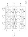
- FIGS. 3A through 3Hshow various portions of a fabrication process to form at least a portion of a memory cell, according to an embodiment.
- the techniques and fabrication processes described hereincan be extended to a number of different apparatuses (e.g., devices).
- fabrication of memory cellswill be described below to retain clarity in the discussions that follow.
- fabrication of floating gate cellsare specifically discussed herein, a person of ordinary skill in the art will recognize, based on the discussions presented herein, that a different charge storage element (e.g., a charge trap) may be fabricated along with or as a substitute for the floating gate.
- FIGS. 3A through 3Hshow both a plan view and a cross-sectional view for additional clarity in understanding the inventive subject matter disclosed herein.
- the process belowdescribes only one memory cell being fabricated, the same process can readily be adapted to any number of memory cells formed atop one another in, for example, a stack (e.g., either on top of a substrate or in a trench).
- a memory devicecan be formed having a high aspect ratio of feature depth to opening of about 30 to 1 or more.
- the process belowdiscloses a substantially toroidal-shaped floating gate, a person of ordinary skill in the art can readily adapt this process to a number of feature types upon reading and understanding the disclosure and figures provided herein.
- the charge storage elementcan take on a number of different shapes and geometries including substantially square, substantially rectangular, and trench-like structures.
- a plan view 300illustrates a first dielectric material 307 with an opening 309 A etched or otherwise formed therethrough.
- Various types or material removal processesare known independently in the art to form the opening 309 A and may include chemical etchants, ion milling (e.g., a reactive ion etch (RIE), laser ablation, and a number of other processes.
- RIEreactive ion etch
- the various removal processescan be used independently of one another, or combined in one or more process activities.
- a cross-sectional view 302is shown to include a substrate 301 , a second dielectric material 303 , and a conductive material 305 A.
- the first dielectric material 307 and the second dielectric material 303are formed substantially parallel to one another and to a surface of the substrate 301 .
- the first dielectric material 307 and the second dielectric material 303can each be the same or similar materials in various embodiments. In other embodiments, the first dielectric material 307 and the second dielectric material 303 can be different materials.
- the various dielectric materialsmay comprise silicon dioxide (SiO 2 ), silicon nitride (Si x N y ), aluminum oxide (Al 2 O 3 ), tantalum pentoxide (Ta 2 O 5 ), hafnium oxide (HfO 2 ), or a variety of other organic or inorganic materials.
- silicon dioxideSiO 2
- silicon nitrideSi x N y
- aluminum oxideAl 2 O 3
- tantalum pentoxideTi 2 O 5
- hafnium oxideHfO 2
- one or more of the various materialsmay include more than one material type.
- the substrate 301can include, for example, any of various substrate types used in the semiconductor and allied industries, which are hereinafter referred to as “semiconductor substrates.”
- substrate typesmay therefore include, but are not limited to, silicon wafers, compound wafers, thin film head assemblies, polyethylene-terephthalate (PET) films deposited or otherwise formed with a semiconducting layer (followed by an annealing activity, such as excimer laser annealing (ELA) in some embodiments), or numerous other types of substrates known independently in the art.
- the substrate 301may comprise a region of a semiconductor material formed over a non-semiconductor material, or vice-versa.
- the substrate 301may be considered to be a silicon wafer.
- the disclosure provided hereina person of ordinary skill in the art will understand how to modify the fabrication activities to account for other types of materials and apparatuses.
- the conductive material 305 Amay be, for example, any of a number of types of conductively doped single-crystal or amorphous semiconductor materials.
- the conductive material 305 Amay be a conductively doped epitaxial deposition of silicon, other elemental semiconductor, or compound semiconductor.
- the conductive material 305 Amay be a conductively doped polysilicon material formed by, for example, thermal decomposition or pyrolysis of silane such a low-pressure chemical vapor deposition (LPCVD) process.
- LPCVDlow-pressure chemical vapor deposition
- Other techniques known independently in the art, such as DC sputtering, followed by a post-anneal activity in some embodiments,may also be utilized.
- the conductive material 305 Ais used to form a control gate of a memory cell.
- a width of the opening 309 Ae.g., a diameter, d 1 , of the opening, may be about 60 nm.
- a thickness, t 1 , of the first dielectric material 307 and a thickness, t 3 , of the second dielectric material 303may be about 200 ⁇ each, and a thickness, t 2 , of the conductive material 305 A can be about 300 ⁇ .
- a ratio of the thickness, t 2 , of the conductive material 305 A to the thickness, t 1 or t 2 , of the first dielectric material 307 or the second dielectric material 303may be about 1.5 to 1.
- a ratio of the width (e.g., diameter, d 1 ) of the opening 309 A to the thickness, t 2 , of the conductive material 305 Amay be about 2 to 1.
- the dimensions and ratios provided throughout this disclosureare by way of example only and are merely provided as an aid in further describing the fabrication process. Each of the dimensions can be varied considerably from the examples given depending upon factors such as the apparatus being fabricated or the design rules employed.
- a plan view 304illustrates an undercut region 311 .
- the cross-sectional view 306illustrates how the conductive material 305 A ( FIG. 3A ) has been recessed (e.g., etched or otherwise stepped back) laterally (e.g., radially) from the opening 309 A to form a recessed control gate 305 B and to expose portions of the first dielectric material 307 and the second dielectric material 303 .
- the conductive material 305 Amay be recessed (e.g., stepped back) by various means such as an anisotropic or isotropic wet etch.
- the recessed control gate 305 Bmay be formed by various types of chemical anisotropic etchants (e.g., tetramethyl ammonium hydroxide (TMAH)). If potassium contamination is not a concern for a particular device type being fabricated, etchants such as such as potassium hydroxide (KOH) may be used as well. Additionally, other chemical etchants may be used for an anisotropic silicon etch. In addition to TMAH and KOH, ethylene-diamene-pyrocatechol (EDP) may also be an effective etchant. As noted, isotropic etchants may also be employed for various types of devices. For example, a hydrofluoric/nitric/acetic (HNA) acid chemical etchant may be used for certain apparatuses or design rules.
- HNAhydrofluoric/nitric/acetic
- the substratecan be protected in various ways such as, for example, forming a barrier region over the substrate 301 prior to forming the second dielectric material.
- a silicon nitride regionmay first be formed over the substrate 301 .
- a selective etchantcan be chosen that etches silicon dioxide faster than silicon nitride. Consequently, formation of the opening 309 A may use the silicon nitride material formed over the substrate 301 as an etch stop.
- the substrate 301may also have a lattice orientation that is more resistant to chemical etching by TMAH, KOH, or other chemical etchants.
- TMAHTMAH
- KOHTMAH
- other chemical etchantsfor example, using a silicon substrate with a ⁇ 110> or ⁇ 101> lattice orientation results in relatively low etch rates with these etchants.
- a silicon dioxide material 313is thermally grown, the formation of which partially consumes exposed portions of the recessed control gate 305 B. Also, assuming the substrate 301 comprises silicon, the silicon dioxide material 313 also partially consumes exposed portions of the substrate 301 . Although a person of ordinary skill in the art will recognize that other types of dielectric material can be substituted for the silicon dioxide material 313 , thermally growing the silicon dioxide material 313 readily forms a dielectric layer over the exposed portions of the recessed control gate 305 B.
- a third dielectric material 315 Ais then formed in the opening 309 A over exposed portions of the first dielectric material 307 and the second dielectric material 303 , followed by forming a fourth dielectric material 317 A in the opening 309 A and over the third dielectric material 315 A.
- the third dielectric material 315 A and the fourth dielectric material 317 Amay comprise the same material, there may be advantages to the third dielectric material 315 A and the fourth dielectric material 317 A being different materials.
- One advantagemay be realized in forming the material as discussed in more detail, by way of example, below with reference to FIG. 3F .
- Another advantagemay arise during less rigorous material removal (e.g., etching) activities that follow.
- the third dielectric material 315 Acan act as an etch stop for the fourth dielectric material 317 A. Therefore, there may be fewer, if any, critical timing activities involved in the fabrication process. Additionally, in some embodiments, the third dielectric material 315 A comprises one or more different materials than the first dielectric material 307 and the second dielectric material 303 , such as for at least the same reasons as discussed above with reference to material selection of the third dielectric material 315 A and the fourth dielectric material 317 A.
- the third dielectric material 315 Amay be silicon nitride and the fourth dielectric material 317 A may be silicon dioxide.
- the third dielectric material 315 Amay, for example, be a conformally deposited silicon nitride.
- the fourth dielectric material 317 Amay, for example, be a thermally grown silicon dioxide material formed over the silicon nitride.
- the silicon dioxide material 313 and the third dielectric material 315 Amay each be formed to a thickness, t 4 , of about 80 ⁇ .
- the fourth dielectric material 317 Amay be formed to a thickness, t 5 , of about 90 ⁇ .
- these dimensionsare by way of example only, used as an aid in understanding the fabrication processes described herein.
- a plan view 312 and a cross-sectional view 314are both shown to include a charge storage element material, such as a semiconductor material 319 A, formed in the opening 309 A.
- the semiconductor material 319 Aat least partially fills the opening 309 A ( FIGS. 3A through 3C ).
- the semiconductor material 319 Ais shown to fill the opening 309 A, a person of ordinary skill in the art will recognize, upon reading and understanding the information disclosed herein, that the semiconductor material 319 A may only partially fill the opening 309 A. Additionally, the semiconductor material 319 A may overfill the opening 309 A.
- the semiconductor material 319 Amay comprise, for example, any of a number of types of single-crystal or amorphous semiconductor materials.
- the semiconductor material 319 Amay be an epitaxial deposition of silicon, other elemental semiconductors, or compound semiconductors.
- the semiconductor material 319 Amay be a conductively-doped polysilicon material.
- a selection of materialmay be partially dependent upon chosen removal (e.g., etching) activities that follow. Further discussion on a choice of material is given below, by way of example, with reference to FIG. 3E .
- a plan view 316illustrates that at least a portion of the semiconductor material 319 A ( FIG. 3D ) has been removed to form a second opening.
- the cross-sectional view 318provides additional detail on the second opening.
- the semiconductor material 319 Ahas been partially removed, forming a floating gate 319 B between portions of the third dielectric material 315 A (and in some cases, such as in the embodiment illustrated in FIG. 3E , portions of the fourth dielectric) covering portions of the first dielectric material 307 and the second dielectric materials 303 that had been exposed during the formation of the recessed control gate 305 B.
- the floating gate 319 Bis shown in FIG.
- the removed portion of the semiconductor material 319 Amay have been, for example, etched by one or more of the various processes discussed above. For example, if the semiconductor material 319 A is a single crystalline material, the removed portion may have been etched by TMAH or KOH, depending upon an orientation of the lattice structure (e.g., ⁇ 100> or ⁇ 111>). If the semiconductor material 319 A is an amorphous semiconductor material, a substantially vertical sidewall etch can be performed by an RIE process.
- a thickness, t 6 , of the floating gate 319 Bmay be about 140 ⁇ .
- a toroidal-shaped featuremay resemble a self-enclosing or doughnut-shaped object.
- the annular shape of a toroidmay be generated by revolving a plane geometrical figure about an axis external to the geometrical figure, where the axis is parallel to the plane of the figure and does not intersect the figure. For example, when a rectangle is rotated around an axis parallel and separated from one of the edges of the rectangle, then a hollow ring-shaped feature, having a rectangular cross-section, is formed.
- the floating gate 319 Bis a toroidal-shaped feature having a substantially rectangular cross-section.
- the floating gate 319 Bfabricated in this example to resemble a toroid with a rectangular cross-sectional, can take on a variety of shapes.
- the cross-sectionmay be circular, ovoid, square, stadium-shaped, or elliptical.
- the fabrication techniques disclosed hereincan also be used to fabricate non-enclosing features.
- a circular, rectangular, or square featurecan be considered to be an enclosing feature since it may be bounded on all sides.
- a trenchmay, in some embodiments, be open on two ends (e.g., an aspect ratio of the length to width of the trench may be high such that the ends are effectively open or the ends may actually be open).
- a trenchmay formed having air gaps.
- a plan view 320illustrates that portions of the third dielectric material 315 A and the fourth dielectric material 317 A have been substantially removed (which, in at least some embodiments, may mean that the portions have been completely removed). Consequently, the floating gate 319 B is now visible from the plan view 320 . Also, the plan view 320 of FIG. 3F is shown to now include a third opening 309 B. An outer periphery of the third opening 309 B is defined by an area surrounded by the floating gate 3199 .
- the third dielectric material 315 A and the fourth dielectric material 317 Amay each have a high dielectric constant. If the removed portions were left in place, the high dielectric constant may cause device performance degradation due to parasitic capacitances of these dielectric materials. Further, in typical floating gate memory cell construction, the floating gate memory cells may have an interference effect from neighboring cells, also caused by the parasitic capacitances.
- portions of the third dielectric material 315 A and the fourth dielectric material 317 A on either side of the floating gate 319 Bparasitic capacitance effects, and the resulting device degradation, can be reduced or eliminated.
- Portions of the third dielectric material 315 A and the fourth dielectric material 317 Amay be removed by, for example, any of the dielectric etchant chemicals discussed, above.
- the third dielectric material 315 A and the fourth dielectric material 317 Awere comprised of silicon nitride and silicon dioxide, respectively, then a silicon dioxide etchant may be used to remove portions of the fourth dielectric material 317 A.
- a silicon nitride etchantmay be used to remove portions of the third dielectric material 315 A. Since each of these dielectric material etchants are generally highly selective with reference to dielectric to semiconductor etching rates, neither etchant should appreciably affect the floating gate 319 B.
- the floating gate 319 Bis toroidal-shaped (e.g., a toroidal-shaped floating gate)
- a remaining portion of the third dielectric material 315 Ai.e., a first dielectric base portion 315 B
- a remaining portion of the fourth dielectric material 317 Ai.e., a second dielectric base portion 317 B
- the floating gate 319 Bis toroidal-shaped (e.g., a toroidal-shaped floating gate)
- a remaining portion of the third dielectric material 315 Ai.e., a first dielectric base portion 315 B
- a remaining portion of the fourth dielectric material 317 Ai.e., a second dielectric base portion 317 B
- the first dielectric base portion 315 B and the second dielectric base portion 317 Bmay serve to, at least in part, secure the floating gate 319 B to the recessed control gate 305 B (e.g., to otherwise prevent toppling of the floating gate 319 B).
- a plan view 324is shown to include a tunnel dielectric 321 and a fourth opening 309 C.
- the fourth opening 309 Chas a reduced width (e.g., diameter) relative to the third opening ( FIG. 3F ) due to the tunnel dielectric 321 being formed in the third opening 309 B and therefore over a sidewall of the floating gate 319 B.
- An outer periphery of the fourth opening 309 Cis defined by an area surrounded by the tunnel dielectric 321 .
- the tunnel dielectric 321is formed over exposed portions of the substrate 301 , and sidewalk of the first dielectric material 307 , the second dielectric material 303 , and the floating gate 319 B. However, as illustrated, the tunnel dielectric 321 is generally unable to fill the gaps left by removed portions of the third dielectric material 315 A and the fourth dielectric material 317 A (see FIG. 3E ). Thus, a first air gap 325 is formed separating a first surface 327 of the floating gate 319 B from the first dielectric material 307 , and a second air gap 329 is formed separating a second surface 331 of the floating gate 319 B from the second dielectric material 303 . As illustrated, the first surface 327 and the second surface 331 may be opposing surfaces.
- the first surface 327 and the second surface 331may also be substantially parallel to surfaces of the first dielectric material 307 and the second dielectric material 303 , respectively.
- the tunnel dielectric 321may be considered to be formed over the first air gap 325 and the second air gap 329 .
- the tunnel dielectric 321may be deposited or otherwise formed to have a thickness, t 7 , of about 30 ⁇ to about 70 ⁇ .
- a ratio of the thickness, t 2 , of the conductive material 305 A ( FIG. 3A ) to the thickness, t 7 , of the tunnel dielectric 321may be from about 10 to 1 to about 4 to 1, or in some embodiments, about 10 to 1 to about 4.2 to 1.
- the tunnel dielectric 321may be a silicon dioxide material, for example, deposited by a number of techniques known independently by a person of ordinary skill in the art such as, for example, high temperature oxidation (HTO) techniques.
- HTOhigh temperature oxidation
- a plan view 328 and a cross-sectional view 330is shown to include a semiconductor material 333 that may then be formed in the fourth opening 309 C ( FIG. 3G ).
- the semiconductor material 333may be used as a channel for a string of memory cells, including the memory cell that includes the depicted charge storage element (e.g., the floating gate 319 B).
- the tunnel dielectric 321may separate the semiconductor material front the charge storage element (e.g., the floating gate 319 B).
- the tunnel dielectric 321may also separate the first air gap 325 and the second air gap 329 from the semiconductor material 333 .
- the dielectric constant of airis substantially less than most dielectric materials, an overall parasitic capacitance level of air is less than most dielectric materials.
- the dielectric constant of silicon dioxideat about 3.9, is considered to be a high dielectric constant (high-k) material.
- the dielectric constant of silicon dioxideis about four times higher than the dielectric constant of air (the dielectric constant of air is about 1.0005). Consequently, the likelihood of degrading parasitic capacitance effects within various memory structures is much higher when silicon dioxide is used, rather than with air.
- parasitic capacitancesare a major source of cell-to-cell interference during program, erase, and read operations of memory cells.
- a low dielectric constant materialmay comprise a material having a dielectric constant less than about 3.5.
- Low-k materialsare known independently to a person of ordinary skill in the art and may include materials such as fluorine-doped silicon dioxide, carbon-doped silicon dioxide, porous silicon dioxide, and various spin-on organic polymer dielectric materials. However, each of these materials only provides an approximately 10% to 45% reduction from the dielectric constant of silicon dioxide.
- one carbon-doped silicon dioxide used in industryis known as Black Diamond® 3 material and has a dielectric constant of about 2.2. Black Diamond® 3 material is produced by Applied Materials, Inc. of Santa Clara, Calif., U.S.A. Consequently, each of these materials will still exhibit a higher parasitic capacitance level than air, due to the higher dielectric constant.
- process activitiesmay refer to particular dielectric materials, such as silicon dioxide, silicon nitride, or others, a person of ordinary skill in the art, after reading this disclosure, will recognize that other dielectric materials may be substituted and still be within a scope of the inventive subject matter.
- dielectric materialssuch as silicon dioxide, silicon nitride, or others
- FIG. 4a block diagram of an illustrative embodiment of an apparatus in the form of a system 407 including one or more memory devices (e.g., the memory device 101 of FIG. 1 ) is shown.
- the system 407may be used in devices such as, for example, a personal digital assistant (PDA), a laptop or portable computer with or without wireless capability, a web tablet, a wireless telephone, a pager, an instant messaging device, a digital music player, a digital camera, or other devices that may be adapted to transmit or receive information either wirelessly or over a wired connection.
- PDApersonal digital assistant
- the system 407may be used in any of the following systems: a wireless local area network (WLAN) system, a wireless personal area network (WPAN) system, or a cellular network.
- WLANwireless local area network
- WPANwireless personal area network
- the system 407 of FIG. 4is shown to include a controller 403 , an input/output (I/O) device 415 (e.g., a keypad, a touchscreen, or a display), the memory device 101 of FIG. 1 , a wireless interface 411 , and a static random access memory (SRAM) device 401 coupled to each other via a bus 409 .
- I/Oinput/output
- a battery 405may supply power to the system 407 in one embodiment.
- the memory device 101may include a NAND memory, a flash memory, a NOR memory, a combination of these, or the like.
- the controller 403may include, for example, one or more microprocessors, digital signal processors, micro-controllers, or the like.
- the memory device 101may be used to store messages transmitted to or by the system 407 .
- the memory device 101may optionally also be used to store instructions that are executed by the controller 403 during operation of the system 407 and may be used to store user data either generated, collected, or received by the system 407 (such as image data).
- the instructionsmay be stored as digital information and the user data, as disclosed herein, may be stored in one section of the memory as digital data and in another section as analog memory. As another example, a given section at one time may be labeled to store digital information and then later may be relabeled and reconfigured to store analog information.
- the I/O device 415may be used to generate a message.
- the system 407may use the wireless interface 411 to transmit and receive messages to and from a wireless communication network with a radio frequency (RF) signal.
- Examples of the wireless interface 411may include an antenna, or a wireless transceiver, such as a dipole antenna.
- the I/O device 415may deliver a voltage reflecting what is stored as either a digital output (if digital information was stored), or as analog information (if analog information was stored). While an example in a wireless application is provided above, embodiments of the inventive subject matter disclosed herein may also be used in non-wireless applications as well.
- FIGS. 5 through 5KThe various illustrations of apparatus (e.g., the memory device 101 and examples of the various fabrication stages illustrated with reference FIGS. 5 through 5K ) are intended to provide a general understanding of the structure of various embodiments and are not intended to provide a complete description of all the elements and features of the apparatus that might make use of the structures, features, and materials described herein.
- the apparatus of the various embodimentsmay include or be included in, for example, electronic circuitry used in high-speed computers, communication and signal processing circuitry, single or multi-processor modules, single or multiple embedded processors, multi-core processors, data switches, and application-specific modules including multilayer, multi-chip modules, or the like.
- Such apparatusesmay further be included as sub-components within a variety of electronic systems, such as televisions, cellular telephones, personal computers (e.g., laptop computers, desktop computers, handheld computers, tablet computers, etc.), workstations, radios, video players, audio players, vehicles, medical devices (e.g., heart monitors, blood pressure monitors, etc.), set top boxes, and various other electronic systems.
Landscapes
- Engineering & Computer Science (AREA)
- Physics & Mathematics (AREA)
- Condensed Matter Physics & Semiconductors (AREA)
- General Physics & Mathematics (AREA)
- Manufacturing & Machinery (AREA)
- Computer Hardware Design (AREA)
- Microelectronics & Electronic Packaging (AREA)
- Power Engineering (AREA)
- Non-Volatile Memory (AREA)
- Semiconductor Memories (AREA)
Abstract
Description
Claims (20)
Priority Applications (3)
| Application Number | Priority Date | Filing Date | Title |
|---|---|---|---|
| US15/620,458US10134597B2 (en) | 2011-08-31 | 2017-06-12 | Apparatuses including memory cells with gaps comprising low dielectric constant materials |
| US16/168,470US10651282B2 (en) | 2011-08-31 | 2018-10-23 | Apparatuses including memory cells with gaps comprising low dielectric constant materials |
| US16/871,600US10985251B2 (en) | 2011-08-31 | 2020-05-11 | Apparatuses including memory cells with gaps comprising low dielectric constant materials |
Applications Claiming Priority (4)
| Application Number | Priority Date | Filing Date | Title |
|---|---|---|---|
| US13/222,367US9136128B2 (en) | 2011-08-31 | 2011-08-31 | Methods and apparatuses including memory cells with air gaps and other low dielectric constant materials |
| US14/825,947US9343316B2 (en) | 2011-08-31 | 2015-08-13 | Methods of forming memory cells with air gaps and other low dielectric constant materials |
| US15/154,467US9679778B2 (en) | 2011-08-31 | 2016-05-13 | Methods of forming memory cells with air gaps and other low dielectric constant materials |
| US15/620,458US10134597B2 (en) | 2011-08-31 | 2017-06-12 | Apparatuses including memory cells with gaps comprising low dielectric constant materials |
Related Parent Applications (1)
| Application Number | Title | Priority Date | Filing Date |
|---|---|---|---|
| US15/154,467ContinuationUS9679778B2 (en) | 2011-08-31 | 2016-05-13 | Methods of forming memory cells with air gaps and other low dielectric constant materials |
Related Child Applications (1)
| Application Number | Title | Priority Date | Filing Date |
|---|---|---|---|
| US16/168,470ContinuationUS10651282B2 (en) | 2011-08-31 | 2018-10-23 | Apparatuses including memory cells with gaps comprising low dielectric constant materials |
Publications (2)
| Publication Number | Publication Date |
|---|---|
| US20170287719A1 US20170287719A1 (en) | 2017-10-05 |
| US10134597B2true US10134597B2 (en) | 2018-11-20 |
Family
ID=47742398
Family Applications (6)
| Application Number | Title | Priority Date | Filing Date |
|---|---|---|---|
| US13/222,367Active2032-04-02US9136128B2 (en) | 2011-08-31 | 2011-08-31 | Methods and apparatuses including memory cells with air gaps and other low dielectric constant materials |
| US14/825,947ActiveUS9343316B2 (en) | 2011-08-31 | 2015-08-13 | Methods of forming memory cells with air gaps and other low dielectric constant materials |
| US15/154,467ActiveUS9679778B2 (en) | 2011-08-31 | 2016-05-13 | Methods of forming memory cells with air gaps and other low dielectric constant materials |
| US15/620,458ActiveUS10134597B2 (en) | 2011-08-31 | 2017-06-12 | Apparatuses including memory cells with gaps comprising low dielectric constant materials |
| US16/168,470ActiveUS10651282B2 (en) | 2011-08-31 | 2018-10-23 | Apparatuses including memory cells with gaps comprising low dielectric constant materials |
| US16/871,600ActiveUS10985251B2 (en) | 2011-08-31 | 2020-05-11 | Apparatuses including memory cells with gaps comprising low dielectric constant materials |
Family Applications Before (3)
| Application Number | Title | Priority Date | Filing Date |
|---|---|---|---|
| US13/222,367Active2032-04-02US9136128B2 (en) | 2011-08-31 | 2011-08-31 | Methods and apparatuses including memory cells with air gaps and other low dielectric constant materials |
| US14/825,947ActiveUS9343316B2 (en) | 2011-08-31 | 2015-08-13 | Methods of forming memory cells with air gaps and other low dielectric constant materials |
| US15/154,467ActiveUS9679778B2 (en) | 2011-08-31 | 2016-05-13 | Methods of forming memory cells with air gaps and other low dielectric constant materials |
Family Applications After (2)
| Application Number | Title | Priority Date | Filing Date |
|---|---|---|---|
| US16/168,470ActiveUS10651282B2 (en) | 2011-08-31 | 2018-10-23 | Apparatuses including memory cells with gaps comprising low dielectric constant materials |
| US16/871,600ActiveUS10985251B2 (en) | 2011-08-31 | 2020-05-11 | Apparatuses including memory cells with gaps comprising low dielectric constant materials |
Country Status (1)
| Country | Link |
|---|---|
| US (6) | US9136128B2 (en) |
Cited By (5)
| Publication number | Priority date | Publication date | Assignee | Title |
|---|---|---|---|---|
| US10446572B2 (en) | 2017-08-11 | 2019-10-15 | Micron Technology, Inc. | Void formation for charge trap structures |
| US10453855B2 (en) | 2017-08-11 | 2019-10-22 | Micron Technology, Inc. | Void formation in charge trap structures |
| US10644105B2 (en) | 2017-08-11 | 2020-05-05 | Micron Technology, Inc. | Memory device including voids between control gates |
| US10651282B2 (en) | 2011-08-31 | 2020-05-12 | Micron Technology, Inc. | Apparatuses including memory cells with gaps comprising low dielectric constant materials |
| US10680006B2 (en) | 2017-08-11 | 2020-06-09 | Micron Technology, Inc. | Charge trap structure with barrier to blocking region |
Families Citing this family (6)
| Publication number | Priority date | Publication date | Assignee | Title |
|---|---|---|---|---|
| KR101094523B1 (en)* | 2010-10-13 | 2011-12-19 | 주식회사 하이닉스반도체 | 3D structure nonvolatile memory device and method of manufacturing same |
| US9793124B2 (en)* | 2014-10-07 | 2017-10-17 | Micron Technology, Inc. | Semiconductor structures |
| US20180261620A1 (en)* | 2017-03-09 | 2018-09-13 | Macronix International Co., Ltd. | Three dimensional memory device and method for fabricating the same |
| US10217794B2 (en) | 2017-05-24 | 2019-02-26 | Globalfoundries Singapore Pte. Ltd. | Integrated circuits with vertical capacitors and methods for producing the same |
| US11711989B2 (en) | 2021-03-23 | 2023-07-25 | International Business Machines Corporation | Phase change memory |
| US12310263B2 (en) | 2021-11-17 | 2025-05-20 | International Business Machines Corporation | Phase change memory gaps |
Citations (31)
| Publication number | Priority date | Publication date | Assignee | Title |
|---|---|---|---|---|
| TW486773B (en) | 2001-05-02 | 2002-05-11 | Taiwan Semiconductor Mfg | Method for forming air gap in bit line structure |
| US7052967B2 (en) | 1999-09-27 | 2006-05-30 | Samsung Electronics Co., Ltd. | Method for fabricating capacitor array preventing crosstalk between adjacent capacitors in semiconductor device |
| US20070184615A1 (en) | 2005-12-30 | 2007-08-09 | Stmicroelectronics S.R.L. | Process for Manufacturing a Non-Volatile Memory Electronic Device Integrated on a Semiconductor Substrate and Corresponding Device |
| US20070257305A1 (en) | 2006-05-01 | 2007-11-08 | Yoshitaka Sasago | Nonvolatile semiconductor memory device and manufacturing method thereof |
| US20070296016A1 (en) | 2006-06-27 | 2007-12-27 | Kabushiki Kaisha Toshiba | Semiconductor device and method of manufacturing the same |
| US20080012061A1 (en) | 2006-04-24 | 2008-01-17 | Masayuki Ichige | Nonvolatile semiconductor memory |
| US20080054341A1 (en) | 2006-08-22 | 2008-03-06 | Katsuaki Natori | Semiconductor memory device and method for manufacturing same |
| US20080197403A1 (en) | 2007-02-07 | 2008-08-21 | Yoshio Ozawa | Semiconductor device |
| US20080283898A1 (en) | 2007-05-14 | 2008-11-20 | Kabushiki Kaisha Toshiba | Non-volatile semiconductor memory device and method of manufacturing the same |
| US20090101883A1 (en) | 2006-10-24 | 2009-04-23 | Macronix International Co., Ltd. | Method for manufacturing a resistor random access memory with a self-aligned air gap insulator |
| US20090302367A1 (en) | 2008-06-10 | 2009-12-10 | Kabushiki Kaisha Toshiba | Method of fabricating semiconductor device and semiconductor device fabricated by the method |
| US20100003795A1 (en) | 2008-07-07 | 2010-01-07 | Hynix Semiconductor, Inc. | Method for Fabricating Flash Memory Device Having Vertical Floating Gate |
| US20100019311A1 (en) | 2008-07-22 | 2010-01-28 | Kabushiki Kaisha Toshiba | Semiconductor memory device and manufacturing method thereof |
| US20100044772A1 (en) | 2005-04-15 | 2010-02-25 | Renesas Technology Corp. | Nonvolatile semiconductor device and method of manufacturing nonvolatile semiconductor device |
| US20100176368A1 (en) | 2009-01-14 | 2010-07-15 | Ko Nikka | Method of manufacturing semiconductor memory device, and semiconductor memory device |
| US20100187593A1 (en) | 2009-01-27 | 2010-07-29 | Kabushiki Kaisha Toshiba | Nand flash memory and method for manufacturing the same |
| US20100295113A1 (en) | 2005-10-31 | 2010-11-25 | Samsung Electronics Co., Ltd. | Semiconductor devices comprising a plurality of gate structures |
| US20110097887A1 (en) | 2008-03-03 | 2011-04-28 | Kabushiki Kaisha Toshiba | Semiconductor storage device and method for manufacturing the same |
| US20110193153A1 (en) | 2010-02-08 | 2011-08-11 | Kabushiki Kaisha Toshiba | Nonvolatile semiconductor memory device |
| US8034693B2 (en) | 2007-11-12 | 2011-10-11 | Panasonic Corporation | Method for fabricating semiconductor device |
| US20110298013A1 (en) | 2010-06-07 | 2011-12-08 | Samsung Electronics Co., Ltd. | Vertical Structure Semiconductor Memory Devices And Methods Of Manufacturing The Same |
| US20110303967A1 (en) | 2010-06-11 | 2011-12-15 | Eli Harari | Non-Volatile Memory With Air Gaps |
| US20110309430A1 (en) | 2010-06-19 | 2011-12-22 | Vinod Robert Purayath | Non-Volatile Memory With Flat Cell Structures And Air Gap Isolation |
| US20110309426A1 (en) | 2010-06-20 | 2011-12-22 | Vinod Robert Purayath | Metal Control Gate Structures And Air Gap Isolation In Non-Volatile Memory |
| US20110309425A1 (en) | 2010-06-19 | 2011-12-22 | Vinod Robert Purayath | Air Gap Isolation In Non-Volatile Memory |
| US20120001252A1 (en)* | 2010-06-30 | 2012-01-05 | Sandisk Corporation | Ultrahigh density vertical nand memory device and method of making thereof |
| US8148789B2 (en) | 2007-10-29 | 2012-04-03 | Kabushiki Kaisha Toshiba | Non-volatile semiconductor storage device and method of manufacturing the same |
| US20120126302A1 (en) | 2010-11-18 | 2012-05-24 | Mitsuhiko Noda | Nonvolatile semiconductor memory device and manufacturing method of the same |
| US20120213006A1 (en) | 2011-02-21 | 2012-08-23 | Kabushiki Kaisha Toshiba | Semiconductor storage device and manufacturing method of semiconductor storage device |
| US20120256247A1 (en)* | 2011-04-11 | 2012-10-11 | Sandisk Corporation | 3D Vertical NAND and Method of Making Thereof by Front and Back Side Processing |
| US20130049093A1 (en) | 2011-08-31 | 2013-02-28 | Minsoo Lee | Methods and apparatuses including memory cells with air gaps and other low dielectric constant materials |
Family Cites Families (49)
| Publication number | Priority date | Publication date | Assignee | Title |
|---|---|---|---|---|
| US5292677A (en) | 1992-09-18 | 1994-03-08 | Micron Technology, Inc. | Reduced mask CMOS process for fabricating stacked capacitor multi-megabit dynamic random access memories utilizing single etch stop layer for contacts |
| TW497120B (en) | 2000-03-06 | 2002-08-01 | Toshiba Corp | Transistor, semiconductor device and manufacturing method of semiconductor device |
| US7253467B2 (en) | 2001-06-28 | 2007-08-07 | Samsung Electronics Co., Ltd. | Non-volatile semiconductor memory devices |
| US6674138B1 (en) | 2001-12-31 | 2004-01-06 | Advanced Micro Devices, Inc. | Use of high-k dielectric materials in modified ONO structure for semiconductor devices |
| US6794764B1 (en) | 2003-03-05 | 2004-09-21 | Advanced Micro Devices, Inc. | Charge-trapping memory arrays resistant to damage from contact hole information |
| KR100855993B1 (en) | 2007-04-03 | 2008-09-02 | 삼성전자주식회사 | Charge trap flash memory device and manufacturing method thereof |
| US20100078758A1 (en) | 2008-09-29 | 2010-04-01 | Sekar Deepak C | Miim diodes |
| JP5515281B2 (en) | 2008-12-03 | 2014-06-11 | ソニー株式会社 | THIN FILM TRANSISTOR, DISPLAY DEVICE, ELECTRONIC DEVICE, AND METHOD FOR PRODUCING THIN FILM TRANSISTOR |
| US8860124B2 (en) | 2009-01-15 | 2014-10-14 | Macronix International Co., Ltd. | Depletion-mode charge-trapping flash device |
| JP5395460B2 (en) | 2009-02-25 | 2014-01-22 | 株式会社東芝 | Nonvolatile semiconductor memory device and manufacturing method thereof |
| US8258034B2 (en) | 2009-08-26 | 2012-09-04 | Micron Technology, Inc. | Charge-trap based memory |
| KR101603731B1 (en) | 2009-09-29 | 2016-03-16 | 삼성전자주식회사 | Vertical nand charge trap flash memory device and method for manufacturing same |
| KR20120007838A (en) | 2010-07-15 | 2012-01-25 | 삼성전자주식회사 | Vertical nonvolatile memory device and manufacturing method thereof |
| KR101699515B1 (en) | 2010-09-01 | 2017-02-14 | 삼성전자주식회사 | Three Dimensional Semiconductor Memory Device And Method Of Fabricating The Same |
| JP5570953B2 (en) | 2010-11-18 | 2014-08-13 | 株式会社東芝 | Nonvolatile semiconductor memory device and method of manufacturing nonvolatile semiconductor memory device |
| JP2012234980A (en) | 2011-05-02 | 2012-11-29 | Toshiba Corp | Nonvolatile semiconductor storage device and manufacturing method of the same |
| KR20120007838U (en) | 2011-05-04 | 2012-11-14 | 김종섭 | Automatic Water Circulation Briquette Boiler |
| JP2013055131A (en) | 2011-09-01 | 2013-03-21 | Toshiba Corp | Nonvolatile semiconductor memory device |
| KR102031182B1 (en) | 2011-11-29 | 2019-10-14 | 삼성전자주식회사 | Semiconductor memory devices and methods for fabricating the same |
| KR20130116607A (en) | 2012-04-16 | 2013-10-24 | 삼성전자주식회사 | Three dimensional semiconductor memory device and method of fabricating the same |
| US8658499B2 (en) | 2012-07-09 | 2014-02-25 | Sandisk Technologies Inc. | Three dimensional NAND device and method of charge trap layer separation and floating gate formation in the NAND device |
| KR101933116B1 (en) | 2012-09-13 | 2018-12-27 | 삼성전자주식회사 | Vertical memory devices and methods of manufacturing the same |
| US8637817B1 (en) | 2013-03-01 | 2014-01-28 | The Rockefeller University | Multi-pole ion trap for mass spectrometry |
| US20150137062A1 (en) | 2013-03-14 | 2015-05-21 | Intermolecular Inc. | Mimcaps with quantum wells as selector elements for crossbar memory arrays |
| KR102190647B1 (en) | 2014-02-24 | 2020-12-14 | 삼성전자주식회사 | Semiconductor Memory Device And Method of Fabricating The Same |
| KR102248205B1 (en) | 2014-06-25 | 2021-05-04 | 삼성전자주식회사 | Semiconductor device having vertical channel and air gap |
| US9177966B1 (en) | 2014-07-08 | 2015-11-03 | Sandisk Technologies Inc. | Three dimensional NAND devices with air gap or low-k core |
| US9666593B2 (en) | 2014-09-29 | 2017-05-30 | Sandisk Technologies Llc | Alternating refractive index in charge-trapping film in three-dimensional memory |
| KR102263121B1 (en) | 2014-12-22 | 2021-06-09 | 에이에스엠 아이피 홀딩 비.브이. | Semiconductor device and manufacuring method thereof |
| US20160343657A1 (en) | 2015-05-22 | 2016-11-24 | Kabushiki Kaisha Toshiba | Semiconductor device and method for manufacturing the same |
| KR102357992B1 (en) | 2015-05-26 | 2022-02-04 | 삼성전자주식회사 | Semiconductor device |
| JP6343256B2 (en) | 2015-05-29 | 2018-06-13 | 東芝メモリ株式会社 | Semiconductor device and manufacturing method thereof |
| US9455261B1 (en) | 2015-07-10 | 2016-09-27 | Micron Technology, Inc. | Integrated structures |
| TWI627733B (en) | 2015-07-24 | 2018-06-21 | 旺宏電子股份有限公司 | Memory device and method for fabricating the same |
| KR102509915B1 (en) | 2015-08-31 | 2023-03-15 | 삼성전자주식회사 | Semiconductor memory device |
| KR102413766B1 (en) | 2015-09-08 | 2022-06-27 | 삼성전자주식회사 | Non-volatile memory device and method for fabricating the same |
| US9997533B2 (en) | 2015-10-06 | 2018-06-12 | Toshiba Memory Corporation | Semiconductor device and method for manufacturing same |
| KR102435524B1 (en) | 2015-10-21 | 2022-08-23 | 삼성전자주식회사 | Semiconductor memory device |
| US9646989B1 (en) | 2015-11-18 | 2017-05-09 | Kabushiki Kaisha Toshiba | Three-dimensional memory device |
| US9570464B1 (en) | 2015-12-15 | 2017-02-14 | Kabushiki Kaisha Toshiba | Method for manufacturing semiconductor device |
| US9865616B2 (en) | 2016-02-09 | 2018-01-09 | Toshiba Memory Corporation | Semiconductor memory device and method for manufacturing same |
| US9679907B1 (en) | 2016-02-29 | 2017-06-13 | Sandisk Technologies Llc | Three-dimensional memory device with charge-trapping-free gate dielectric for top select gate electrode and method of making thereof |
| US20170278851A1 (en) | 2016-03-23 | 2017-09-28 | Kabushiki Kaisha Toshiba | Semiconductor memory device |
| US9748262B1 (en) | 2016-04-13 | 2017-08-29 | Macronix International Co., Ltd. | Memory structure and manufacturing method of the same |
| US9859298B1 (en) | 2016-06-23 | 2018-01-02 | Sandisk Technologies Llc | Amorphous silicon layer in memory device which reduces neighboring word line interference |
| US10453855B2 (en) | 2017-08-11 | 2019-10-22 | Micron Technology, Inc. | Void formation in charge trap structures |
| US10164009B1 (en) | 2017-08-11 | 2018-12-25 | Micron Technology, Inc. | Memory device including voids between control gates |
| US10446572B2 (en) | 2017-08-11 | 2019-10-15 | Micron Technology, Inc. | Void formation for charge trap structures |
| US10680006B2 (en) | 2017-08-11 | 2020-06-09 | Micron Technology, Inc. | Charge trap structure with barrier to blocking region |
- 2011
- 2011-08-31USUS13/222,367patent/US9136128B2/enactiveActive
- 2015
- 2015-08-13USUS14/825,947patent/US9343316B2/enactiveActive
- 2016
- 2016-05-13USUS15/154,467patent/US9679778B2/enactiveActive
- 2017
- 2017-06-12USUS15/620,458patent/US10134597B2/enactiveActive
- 2018
- 2018-10-23USUS16/168,470patent/US10651282B2/enactiveActive
- 2020
- 2020-05-11USUS16/871,600patent/US10985251B2/enactiveActive
Patent Citations (41)
| Publication number | Priority date | Publication date | Assignee | Title |
|---|---|---|---|---|
| US7052967B2 (en) | 1999-09-27 | 2006-05-30 | Samsung Electronics Co., Ltd. | Method for fabricating capacitor array preventing crosstalk between adjacent capacitors in semiconductor device |
| TW486773B (en) | 2001-05-02 | 2002-05-11 | Taiwan Semiconductor Mfg | Method for forming air gap in bit line structure |
| US20100044772A1 (en) | 2005-04-15 | 2010-02-25 | Renesas Technology Corp. | Nonvolatile semiconductor device and method of manufacturing nonvolatile semiconductor device |
| US20100190330A1 (en)* | 2005-04-15 | 2010-07-29 | Renesas Technology Corp. | Nonvolatile semiconductor device and method of manufacturing nonvolatile semiconductor device |
| US20100295113A1 (en) | 2005-10-31 | 2010-11-25 | Samsung Electronics Co., Ltd. | Semiconductor devices comprising a plurality of gate structures |
| US20070184615A1 (en) | 2005-12-30 | 2007-08-09 | Stmicroelectronics S.R.L. | Process for Manufacturing a Non-Volatile Memory Electronic Device Integrated on a Semiconductor Substrate and Corresponding Device |
| US20080012061A1 (en) | 2006-04-24 | 2008-01-17 | Masayuki Ichige | Nonvolatile semiconductor memory |
| US20110108905A1 (en)* | 2006-04-24 | 2011-05-12 | Masayuki Ichige | Nonvolatile semiconductor memory |
| US20070257305A1 (en) | 2006-05-01 | 2007-11-08 | Yoshitaka Sasago | Nonvolatile semiconductor memory device and manufacturing method thereof |
| US20070296016A1 (en) | 2006-06-27 | 2007-12-27 | Kabushiki Kaisha Toshiba | Semiconductor device and method of manufacturing the same |
| US20080054341A1 (en) | 2006-08-22 | 2008-03-06 | Katsuaki Natori | Semiconductor memory device and method for manufacturing same |
| US20090101883A1 (en) | 2006-10-24 | 2009-04-23 | Macronix International Co., Ltd. | Method for manufacturing a resistor random access memory with a self-aligned air gap insulator |
| US20080197403A1 (en) | 2007-02-07 | 2008-08-21 | Yoshio Ozawa | Semiconductor device |
| US7999304B2 (en)* | 2007-02-07 | 2011-08-16 | Kabushiki Kaisha Toshiba | Semiconductor device |
| US20080283898A1 (en) | 2007-05-14 | 2008-11-20 | Kabushiki Kaisha Toshiba | Non-volatile semiconductor memory device and method of manufacturing the same |
| US8148789B2 (en) | 2007-10-29 | 2012-04-03 | Kabushiki Kaisha Toshiba | Non-volatile semiconductor storage device and method of manufacturing the same |
| US8034693B2 (en) | 2007-11-12 | 2011-10-11 | Panasonic Corporation | Method for fabricating semiconductor device |
| US20110097887A1 (en) | 2008-03-03 | 2011-04-28 | Kabushiki Kaisha Toshiba | Semiconductor storage device and method for manufacturing the same |
| US20090302367A1 (en) | 2008-06-10 | 2009-12-10 | Kabushiki Kaisha Toshiba | Method of fabricating semiconductor device and semiconductor device fabricated by the method |
| US20110104883A1 (en)* | 2008-06-10 | 2011-05-05 | Kabushiki Kaisha Toshiba | Method of fabricating semiconductor device |
| US20100003795A1 (en) | 2008-07-07 | 2010-01-07 | Hynix Semiconductor, Inc. | Method for Fabricating Flash Memory Device Having Vertical Floating Gate |
| US20100019311A1 (en) | 2008-07-22 | 2010-01-28 | Kabushiki Kaisha Toshiba | Semiconductor memory device and manufacturing method thereof |
| US20110300703A1 (en)* | 2008-07-22 | 2011-12-08 | Kabushiki Kaisha Toshiba | Semiconductor memory device and manufacturing method thereof |
| US20100176368A1 (en) | 2009-01-14 | 2010-07-15 | Ko Nikka | Method of manufacturing semiconductor memory device, and semiconductor memory device |
| US20100187593A1 (en) | 2009-01-27 | 2010-07-29 | Kabushiki Kaisha Toshiba | Nand flash memory and method for manufacturing the same |
| US20110193153A1 (en) | 2010-02-08 | 2011-08-11 | Kabushiki Kaisha Toshiba | Nonvolatile semiconductor memory device |
| US20110298013A1 (en) | 2010-06-07 | 2011-12-08 | Samsung Electronics Co., Ltd. | Vertical Structure Semiconductor Memory Devices And Methods Of Manufacturing The Same |
| US20110303967A1 (en) | 2010-06-11 | 2011-12-15 | Eli Harari | Non-Volatile Memory With Air Gaps |
| US20110309425A1 (en) | 2010-06-19 | 2011-12-22 | Vinod Robert Purayath | Air Gap Isolation In Non-Volatile Memory |
| US20110309430A1 (en) | 2010-06-19 | 2011-12-22 | Vinod Robert Purayath | Non-Volatile Memory With Flat Cell Structures And Air Gap Isolation |
| US20110309426A1 (en) | 2010-06-20 | 2011-12-22 | Vinod Robert Purayath | Metal Control Gate Structures And Air Gap Isolation In Non-Volatile Memory |
| US20120001252A1 (en)* | 2010-06-30 | 2012-01-05 | Sandisk Corporation | Ultrahigh density vertical nand memory device and method of making thereof |
| US20120126302A1 (en) | 2010-11-18 | 2012-05-24 | Mitsuhiko Noda | Nonvolatile semiconductor memory device and manufacturing method of the same |
| US20120213006A1 (en) | 2011-02-21 | 2012-08-23 | Kabushiki Kaisha Toshiba | Semiconductor storage device and manufacturing method of semiconductor storage device |
| US20120256247A1 (en)* | 2011-04-11 | 2012-10-11 | Sandisk Corporation | 3D Vertical NAND and Method of Making Thereof by Front and Back Side Processing |
| US20130049093A1 (en) | 2011-08-31 | 2013-02-28 | Minsoo Lee | Methods and apparatuses including memory cells with air gaps and other low dielectric constant materials |
| US9136128B2 (en) | 2011-08-31 | 2015-09-15 | Micron Technology, Inc. | Methods and apparatuses including memory cells with air gaps and other low dielectric constant materials |
| US20150348790A1 (en) | 2011-08-31 | 2015-12-03 | Micron Technology, Inc. | Methods and apparatuses including memory cells with air gaps and other low dielectric constant materials |
| US9343316B2 (en) | 2011-08-31 | 2016-05-17 | Micron Technology, Inc. | Methods of forming memory cells with air gaps and other low dielectric constant materials |
| US20160254159A1 (en) | 2011-08-31 | 2016-09-01 | Micron Technology, Inc. | Methods of forming memory cells with air gaps and other low dielectric constant materials |
| US9679778B2 (en) | 2011-08-31 | 2017-06-13 | Micron Technology, Inc. | Methods of forming memory cells with air gaps and other low dielectric constant materials |
Non-Patent Citations (1)
| Title |
|---|
| Tsukamoto, Keisuke, et al., "Advanced Air Gap Process for Multi-Level-Cell Flash Memories Reducing Threshold Voltage Interference and Realizing High Reliability", Jpn. J. Appl. Phys. 46, (2007), 1. |
Cited By (14)
| Publication number | Priority date | Publication date | Assignee | Title |
|---|---|---|---|---|
| US10985251B2 (en) | 2011-08-31 | 2021-04-20 | Micron Technology, Inc. | Apparatuses including memory cells with gaps comprising low dielectric constant materials |
| US10651282B2 (en) | 2011-08-31 | 2020-05-12 | Micron Technology, Inc. | Apparatuses including memory cells with gaps comprising low dielectric constant materials |
| US11923407B2 (en) | 2017-08-11 | 2024-03-05 | Micron Technology, Inc. | Memory device including voids between control gates |
| US10644105B2 (en) | 2017-08-11 | 2020-05-05 | Micron Technology, Inc. | Memory device including voids between control gates |
| US10680006B2 (en) | 2017-08-11 | 2020-06-09 | Micron Technology, Inc. | Charge trap structure with barrier to blocking region |
| US10937802B2 (en) | 2017-08-11 | 2021-03-02 | Micron Technology, Inc. | Void formation for charge trap structures |
| US11329127B2 (en) | 2017-08-11 | 2022-05-10 | Micron Technology, Inc. | Memory device including voids between control gates |
| US10446572B2 (en) | 2017-08-11 | 2019-10-15 | Micron Technology, Inc. | Void formation for charge trap structures |
| US10453855B2 (en) | 2017-08-11 | 2019-10-22 | Micron Technology, Inc. | Void formation in charge trap structures |
| US11393843B2 (en) | 2017-08-11 | 2022-07-19 | Micron Technology, Inc. | Charge trap structure with barrier to blocking region |
| US11569255B2 (en) | 2017-08-11 | 2023-01-31 | Micron Technology, Inc. | Void formation in charge trap structures |
| US11765903B2 (en) | 2017-08-11 | 2023-09-19 | Micron Technology, Inc. | Charge trap structure with barrier to blocking region |
| US11037951B2 (en) | 2017-08-11 | 2021-06-15 | Micron Technology, Inc. | Void formation in charge trap structures |
| US11943924B2 (en) | 2017-08-11 | 2024-03-26 | Micron Technology, Inc. | Void formation for charge trap structures |
Also Published As
| Publication number | Publication date |
|---|---|
| US20190157092A1 (en) | 2019-05-23 |
| US20200279928A1 (en) | 2020-09-03 |
| US9343316B2 (en) | 2016-05-17 |
| US20170287719A1 (en) | 2017-10-05 |
| US20150348790A1 (en) | 2015-12-03 |
| US20130049093A1 (en) | 2013-02-28 |
| US10985251B2 (en) | 2021-04-20 |
| US9136128B2 (en) | 2015-09-15 |
| US20160254159A1 (en) | 2016-09-01 |
| US9679778B2 (en) | 2017-06-13 |
| US10651282B2 (en) | 2020-05-12 |
Similar Documents
| Publication | Publication Date | Title |
|---|---|---|
| US10985251B2 (en) | Apparatuses including memory cells with gaps comprising low dielectric constant materials | |
| US11018135B2 (en) | Three-dimensional devices having reduced contact length | |
| US11244725B2 (en) | Apparatuses and methods of forming apparatuses using a partial deck-by-deck process flow | |
| US8912589B2 (en) | Methods and apparatuses including strings of memory cells formed along levels of semiconductor material | |
| US8643084B2 (en) | Vertical non-volatile memory device | |
| WO2021155557A1 (en) | Varying channel width in three-dimensional memory array | |
| US11322388B2 (en) | Semiconductor structure formation | |
| US11469103B2 (en) | Semiconductor structure formation | |
| US20240407173A1 (en) | Semiconductor memory devices and methods of manufacturing thereof | |
| US20230354585A1 (en) | Digit line and cell contact isolation | |
| US11910601B2 (en) | Microelectronic devices with source region vertically between tiered decks, and related methods and systems | |
| TWI544579B (en) | Memory unit with isolated charge portion and method of manufacturing same | |
| US20240064962A1 (en) | Doped dielectric material |
Legal Events
| Date | Code | Title | Description |
|---|---|---|---|
| AS | Assignment | Owner name:MORGAN STANLEY SENIOR FUNDING, INC., AS COLLATERAL Free format text:SUPPLEMENT NO. 6 TO PATENT SECURITY AGREEMENT;ASSIGNOR:MICRON TECHNOLOGY, INC.;REEL/FRAME:044653/0333 3 Effective date:20171023 Owner name:U.S. BANK NATIONAL ASSOCIATION, AS COLLATERAL AGEN Free format text:SUPPLEMENT NO. 6 TO PATENT SECURITY AGREEMENT;ASSIGNOR:MICRON TECHNOLOGY, INC.;REEL/FRAME:044348/0253 3 Effective date:20171023 Owner name:U.S. BANK NATIONAL ASSOCIATION, AS COLLATERAL AGENT, MINNESOTA Free format text:SUPPLEMENT NO. 6 TO PATENT SECURITY AGREEMENT;ASSIGNOR:MICRON TECHNOLOGY, INC.;REEL/FRAME:044348/0253 Effective date:20171023 Owner name:MORGAN STANLEY SENIOR FUNDING, INC., AS COLLATERAL AGENT, MARYLAND Free format text:SUPPLEMENT NO. 6 TO PATENT SECURITY AGREEMENT;ASSIGNOR:MICRON TECHNOLOGY, INC.;REEL/FRAME:044653/0333 Effective date:20171023 Owner name:U.S. BANK NATIONAL ASSOCIATION, AS COLLATERAL AGEN Free format text:SUPPLEMENT NO. 6 TO PATENT SECURITY AGREEMENT;ASSIGNOR:MICRON TECHNOLOGY, INC.;REEL/FRAME:044348/0253 Effective date:20171023 Owner name:MORGAN STANLEY SENIOR FUNDING, INC., AS COLLATERAL Free format text:SUPPLEMENT NO. 6 TO PATENT SECURITY AGREEMENT;ASSIGNOR:MICRON TECHNOLOGY, INC.;REEL/FRAME:044653/0333 Effective date:20171023 | |
| AS | Assignment | Owner name:JPMORGAN CHASE BANK, N.A., AS COLLATERAL AGENT, ILLINOIS Free format text:SECURITY INTEREST;ASSIGNORS:MICRON TECHNOLOGY, INC.;MICRON SEMICONDUCTOR PRODUCTS, INC.;REEL/FRAME:047540/0001 Effective date:20180703 Owner name:JPMORGAN CHASE BANK, N.A., AS COLLATERAL AGENT, IL Free format text:SECURITY INTEREST;ASSIGNORS:MICRON TECHNOLOGY, INC.;MICRON SEMICONDUCTOR PRODUCTS, INC.;REEL/FRAME:047540/0001 Effective date:20180703 | |
| AS | Assignment | Owner name:MICRON TECHNOLOGY, INC., IDAHO Free format text:RELEASE BY SECURED PARTY;ASSIGNOR:U.S. BANK NATIONAL ASSOCIATION, AS AGENT;REEL/FRAME:046597/0333 Effective date:20180629 | |
| STCF | Information on status: patent grant | Free format text:PATENTED CASE | |
| AS | Assignment | Owner name:MICRON TECHNOLOGY, INC., CALIFORNIA Free format text:RELEASE BY SECURED PARTY;ASSIGNOR:MORGAN STANLEY SENIOR FUNDING, INC., AS COLLATERAL AGENT;REEL/FRAME:050709/0838 Effective date:20190731 | |
| AS | Assignment | Owner name:MICRON SEMICONDUCTOR PRODUCTS, INC., IDAHO Free format text:RELEASE BY SECURED PARTY;ASSIGNOR:JPMORGAN CHASE BANK, N.A., AS COLLATERAL AGENT;REEL/FRAME:051028/0001 Effective date:20190731 Owner name:MICRON TECHNOLOGY, INC., IDAHO Free format text:RELEASE BY SECURED PARTY;ASSIGNOR:JPMORGAN CHASE BANK, N.A., AS COLLATERAL AGENT;REEL/FRAME:051028/0001 Effective date:20190731 | |
| MAFP | Maintenance fee payment | Free format text:PAYMENT OF MAINTENANCE FEE, 4TH YEAR, LARGE ENTITY (ORIGINAL EVENT CODE: M1551); ENTITY STATUS OF PATENT OWNER: LARGE ENTITY Year of fee payment:4 |