US10121539B2 - Memory systems and memory programming methods - Google Patents
Memory systems and memory programming methodsDownload PDFInfo
- Publication number
- US10121539B2 US10121539B2US15/495,808US201715495808AUS10121539B2US 10121539 B2US10121539 B2US 10121539B2US 201715495808 AUS201715495808 AUS 201715495808AUS 10121539 B2US10121539 B2US 10121539B2
- Authority
- US
- United States
- Prior art keywords
- memory
- memory cell
- program
- different
- state
- Prior art date
- Legal status (The legal status is an assumption and is not a legal conclusion. Google has not performed a legal analysis and makes no representation as to the accuracy of the status listed.)
- Active
Links
- 230000015654memoryEffects0.000titleclaimsabstractdescription504
- 238000000034methodMethods0.000titleclaimsabstractdescription19
- 238000001514detection methodMethods0.000claimsabstractdescription17
- 239000003989dielectric materialSubstances0.000claimsdescription9
- 239000000463materialSubstances0.000description4
- 238000012795verificationMethods0.000description4
- 239000010949copperSubstances0.000description3
- 230000000717retained effectEffects0.000description3
- 230000015572biosynthetic processEffects0.000description2
- 239000004020conductorSubstances0.000description2
- 238000010586diagramMethods0.000description2
- 150000002500ionsChemical class0.000description2
- 229910017107AlOxInorganic materials0.000description1
- RYGMFSIKBFXOCR-UHFFFAOYSA-NCopperChemical compound[Cu]RYGMFSIKBFXOCR-UHFFFAOYSA-N0.000description1
- 229910002531CuTeInorganic materials0.000description1
- -1HfOxInorganic materials0.000description1
- NRTOMJZYCJJWKI-UHFFFAOYSA-NTitanium nitrideChemical compound[Ti]#NNRTOMJZYCJJWKI-UHFFFAOYSA-N0.000description1
- 229910003134ZrOxInorganic materials0.000description1
- 230000000295complement effectEffects0.000description1
- 229910052802copperInorganic materials0.000description1
- 230000003247decreasing effectEffects0.000description1
- 230000000977initiatory effectEffects0.000description1
- 230000000630rising effectEffects0.000description1
- 238000010408sweepingMethods0.000description1
- 210000003813thumbAnatomy0.000description1
Images


Classifications
- G—PHYSICS
- G11—INFORMATION STORAGE
- G11C—STATIC STORES
- G11C13/00—Digital stores characterised by the use of storage elements not covered by groups G11C11/00, G11C23/00, or G11C25/00
- G11C13/0002—Digital stores characterised by the use of storage elements not covered by groups G11C11/00, G11C23/00, or G11C25/00 using resistive RAM [RRAM] elements
- G11C13/0021—Auxiliary circuits
- G11C13/0069—Writing or programming circuits or methods
- G—PHYSICS
- G11—INFORMATION STORAGE
- G11C—STATIC STORES
- G11C11/00—Digital stores characterised by the use of particular electric or magnetic storage elements; Storage elements therefor
- G11C11/02—Digital stores characterised by the use of particular electric or magnetic storage elements; Storage elements therefor using magnetic elements
- G11C11/16—Digital stores characterised by the use of particular electric or magnetic storage elements; Storage elements therefor using magnetic elements using elements in which the storage effect is based on magnetic spin effect
- G—PHYSICS
- G11—INFORMATION STORAGE
- G11C—STATIC STORES
- G11C13/00—Digital stores characterised by the use of storage elements not covered by groups G11C11/00, G11C23/00, or G11C25/00
- G11C13/0002—Digital stores characterised by the use of storage elements not covered by groups G11C11/00, G11C23/00, or G11C25/00 using resistive RAM [RRAM] elements
- G11C13/0009—RRAM elements whose operation depends upon chemical change
- G11C13/0011—RRAM elements whose operation depends upon chemical change comprising conductive bridging RAM [CBRAM] or programming metallization cells [PMCs]
- G—PHYSICS
- G11—INFORMATION STORAGE
- G11C—STATIC STORES
- G11C13/00—Digital stores characterised by the use of storage elements not covered by groups G11C11/00, G11C23/00, or G11C25/00
- G11C13/0002—Digital stores characterised by the use of storage elements not covered by groups G11C11/00, G11C23/00, or G11C25/00 using resistive RAM [RRAM] elements
- G11C13/0021—Auxiliary circuits
- G11C13/004—Reading or sensing circuits or methods
- G—PHYSICS
- G11—INFORMATION STORAGE
- G11C—STATIC STORES
- G11C13/00—Digital stores characterised by the use of storage elements not covered by groups G11C11/00, G11C23/00, or G11C25/00
- G11C13/0002—Digital stores characterised by the use of storage elements not covered by groups G11C11/00, G11C23/00, or G11C25/00 using resistive RAM [RRAM] elements
- G11C13/0021—Auxiliary circuits
- G11C13/0064—Verifying circuits or methods
- G—PHYSICS
- G11—INFORMATION STORAGE
- G11C—STATIC STORES
- G11C13/00—Digital stores characterised by the use of storage elements not covered by groups G11C11/00, G11C23/00, or G11C25/00
- G11C13/0002—Digital stores characterised by the use of storage elements not covered by groups G11C11/00, G11C23/00, or G11C25/00 using resistive RAM [RRAM] elements
- G11C13/0021—Auxiliary circuits
- G11C13/004—Reading or sensing circuits or methods
- G11C2013/0054—Read is performed on a reference element, e.g. cell, and the reference sensed value is used to compare the sensed value of the selected cell
- G—PHYSICS
- G11—INFORMATION STORAGE
- G11C—STATIC STORES
- G11C13/00—Digital stores characterised by the use of storage elements not covered by groups G11C11/00, G11C23/00, or G11C25/00
- G11C13/0002—Digital stores characterised by the use of storage elements not covered by groups G11C11/00, G11C23/00, or G11C25/00 using resistive RAM [RRAM] elements
- G11C13/0021—Auxiliary circuits
- G11C13/0064—Verifying circuits or methods
- G11C2013/0066—Verify correct writing whilst writing is in progress, e.g. by detecting onset or cessation of current flow in cell and using the detector output to terminate writing
- G—PHYSICS
- G11—INFORMATION STORAGE
- G11C—STATIC STORES
- G11C13/00—Digital stores characterised by the use of storage elements not covered by groups G11C11/00, G11C23/00, or G11C25/00
- G11C13/0002—Digital stores characterised by the use of storage elements not covered by groups G11C11/00, G11C23/00, or G11C25/00 using resistive RAM [RRAM] elements
- G11C13/0021—Auxiliary circuits
- G11C13/0069—Writing or programming circuits or methods
- G11C2013/0071—Write using write potential applied to access device gate
- G—PHYSICS
- G11—INFORMATION STORAGE
- G11C—STATIC STORES
- G11C13/00—Digital stores characterised by the use of storage elements not covered by groups G11C11/00, G11C23/00, or G11C25/00
- G11C13/0002—Digital stores characterised by the use of storage elements not covered by groups G11C11/00, G11C23/00, or G11C25/00 using resistive RAM [RRAM] elements
- G11C13/0021—Auxiliary circuits
- G11C13/0069—Writing or programming circuits or methods
- G11C2013/0076—Write operation performed depending on read result
- G—PHYSICS
- G11—INFORMATION STORAGE
- G11C—STATIC STORES
- G11C13/00—Digital stores characterised by the use of storage elements not covered by groups G11C11/00, G11C23/00, or G11C25/00
- G11C13/0002—Digital stores characterised by the use of storage elements not covered by groups G11C11/00, G11C23/00, or G11C25/00 using resistive RAM [RRAM] elements
- G11C13/0021—Auxiliary circuits
- G11C13/0069—Writing or programming circuits or methods
- G11C2013/0078—Write using current through the cell
- G—PHYSICS
- G11—INFORMATION STORAGE
- G11C—STATIC STORES
- G11C13/00—Digital stores characterised by the use of storage elements not covered by groups G11C11/00, G11C23/00, or G11C25/00
- G11C13/0002—Digital stores characterised by the use of storage elements not covered by groups G11C11/00, G11C23/00, or G11C25/00 using resistive RAM [RRAM] elements
- G11C13/0021—Auxiliary circuits
- G11C13/0069—Writing or programming circuits or methods
- G11C2013/0092—Write characterized by the shape, e.g. form, length, amplitude of the write pulse
- G—PHYSICS
- G11—INFORMATION STORAGE
- G11C—STATIC STORES
- G11C2213/00—Indexing scheme relating to G11C13/00 for features not covered by this group
- G11C2213/30—Resistive cell, memory material aspects
- G11C2213/34—Material includes an oxide or a nitride
- G—PHYSICS
- G11—INFORMATION STORAGE
- G11C—STATIC STORES
- G11C2213/00—Indexing scheme relating to G11C13/00 for features not covered by this group
- G11C2213/50—Resistive cell structure aspects
- G11C2213/55—Structure including two electrodes, a memory active layer and at least two other layers which can be a passive or source or reservoir layer or a less doped memory active layer
- G—PHYSICS
- G11—INFORMATION STORAGE
- G11C—STATIC STORES
- G11C2213/00—Indexing scheme relating to G11C13/00 for features not covered by this group
- G11C2213/70—Resistive array aspects
- G11C2213/79—Array wherein the access device being a transistor
Definitions
- Embodiments disclosed hereinpertain to memory systems and memory programming methods.
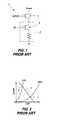
- a conventional memory circuit 1 including a memory cell 2is shown in FIG. 1 .
- the illustrated memory circuit 1performs programming of the memory cell 2 including programming the memory cell to set and reset memory states.
- a transistor 3applies signals to the memory cell 2 to program the memory cell 2 to the different memory states.
- a voltage potentialmay be applied to the memory cell 2 to program the memory cell 2 from a set to a reset state.
- Vcellcell current and cell voltage
- LRSlow electrical resistance state
- HRShigh electrical resistance state
- a plurality of operation points 6 , 7are provided at intersections of a load line 5 of the circuitry of FIG. 1 with the LRS and HRS curves of the memory cell.
- the memory cell 2changes from the low electrical resistance state to the high electrical resistance state.
- the current or voltageis initially controlled at the beginning of the programming between the low to high resistance states, then the current or voltage is at operation point 7 when the cell 2 is in the high resistance state and which may not be controlled. Likewise, if the current or voltage is controlled when the cell 2 is in the high resistance state, then the current or voltage is at operation point 6 when the cell 2 is in the low resistance state and which may not be controlled.
- At least some embodimentsare directed towards memories, memory systems and memory programming methods which provide increased flexibility of memory cell programming compared with some conventional arrangements.
- FIG. 1is a schematic representation of conventional memory circuitry.
- FIG. 2is a graphical representation of characteristics of the conventional memory cell of FIG. 1 in different memory states.
- FIG. 3is a functional block diagram of a memory system according to one embodiment.
- FIG. 4is an illustrative representation of a memory cell according to one embodiment.
- FIG. 5is a graphical representation of plural memory states of a memory cell according to one embodiment.
- FIG. 6is a schematic representation of a plurality of memory cells in an array according to one embodiment.
- FIG. 7is an illustrative representation of a tile of a memory chip according to one embodiment.
- FIG. 8is a schematic representation of program circuitry and a memory cell according to one embodiment.
- FIG. 9is a graphical representation of electrical characteristics of the memory cell of FIG. 8 according to one embodiment.
- FIG. 10is a schematic representation of program circuitry and a memory cell according to one embodiment.
- FIG. 11is a schematic representation of sense amplifier and write driver circuitry according to one embodiment.
- At least some embodimentsdisclose memories, memory systems and methods of programming memories from one memory state to another memory state.
- One more specific embodimentpertains to programming resistive non-volatile memory where individual memory cells have different electrical resistances corresponding to different memory states.
- a plurality of different program signalsmay be applied to a memory cell during a single programming operation to change the programming of the memory cell from one resistive state (e.g., low electrical resistance) to another resistive state (e.g., high electrical resistance).
- the different program signalsindependently control programming parameters, such as current through the memory cell or voltage across the memory cell, during initial and subsequent programming of the memory cell to implement the single programming operation between the different memory states. Additional details of these and further embodiments are described below.
- FIG. 3a functional block diagram of a memory system 10 is shown according to one embodiment.
- the illustrated memory system 10includes a controller 12 , access circuitry 14 , and memory 16 .
- Memory system 10may be implemented within or with respect to various associated devices (not shown), such as computers, cameras, media players, and thumb drives, in some examples.
- Memory system 10stores data generated or utilized by the associated devices in the described examples.
- Other embodiments of memory system 10are possible and may include more, less and/or alternative components or circuitry.
- Controller 12controls operations of writing, reading and re-writing data of memory 16 as well as interfacing with other components or circuitry, such as sources of data to be stored within memory 16 .
- Controller 12may access and process commands with respect to memory 16 during operations of an associated device.
- Example commandsinstruct the generation of program reset and set voltage potentials which are applied to memory 16 in one embodiment.
- the reset and set operationsare used to write data to memory 16 (i.e., program the memory) and are both referred to as write operations in one embodiment.
- Controller 12may also control the application of read and verify pulses to memory 16 to read and verify stored data in one embodiment.
- controller 12is configured to process data, control data access and storage, issue commands, and control other desired operations.
- Controller 12may comprise processing circuitry configured to execute programming provided by appropriate computer-readable storage media (e.g., memory) in at least one embodiment.
- the controller 12may be implemented as one or more microcontroller(s), processor(s) and/or other structure configured to execute executable instructions including, for example, software and/or firmware instructions.
- Other example embodiments of controller 12may include hardware logic, PGA, FPGA, ASIC, state machines, and/or other structures alone or in combination with one or more processor(s). These examples of controller 12 are for illustration and other configurations are possible.
- Access circuitry 14is coupled with controller 12 and memory 16 and is configured to implement addressing (selection of columns and rows of memory 16 ), writing, reading, verifying and re-writing operations with respect to memory cells of memory 16 in one embodiment.
- access circuitry 14may receive instructions from controller 12 to select a specific block, page, word or byte of the memory 16 as well as to implement writing, reading, verifying and re-writing with respect to a plurality of cells of the selected block, page, word or byte.
- the access circuitry 14may apply electrical voltage potentials to the memory 16 to perform write, read and verification operations in one embodiment.
- Memory 16includes a plurality of memory cells configured to store data, conductors electrically connected with the memory cells, and perhaps additional circuitry, for example circuits of the access circuitry 14 . At least some of the memory cells are individually capable of being programmed to a plurality of different memory states at a plurality of moments in time. Memory 16 is accessible to the user and/or associated device for storage of digital information.
- the memory cellsmay be configured as non-volatile cells in some implementations and may have different electrical resistances corresponding to different memory states.
- memory 16is implemented as conductive-bridge random access memory (CBRAM) and the memory cells are conductive-bridge memory cells.
- CBRAMconductive-bridge random access memory
- Memory 16may be implemented in different arrangements in different embodiments.
- the memory 16may be implemented within a memory device, such as a chip, a portion of the chip (e.g., tiles and/or sub-tiles discussed below) or other arrangements.
- the memory devicemay also include controller 12 and/or access circuitry 14 or portions thereof.
- the illustrated example memory cell 20is a one transistor/one resistor (1T1R) CBRAM memory cell.
- Other types of memory cellsmay be utilized in other embodiments, such as other types of resistive memory in one example.
- the example memory cell 20includes a top electrode 22 , memory element 21 and bottom electrode 24 .
- Top and bottom electrodes 22 , 24comprise electrically conductive material and may also be referred to as first and second electrodes (or vice versa) of the memory cell 20 in one embodiment.
- the illustrated embodiment of memory element 21includes an electrically conductive source member or layer 26 and a dielectric layer 28 intermediate the electrodes 22 , 24 .
- the source layer 26is a Cu+ source layer (e.g., CuTe)
- example materials of the dielectric layer 28include AlOx, HfOx, and ZrOx
- the bottom electrode 24is titanium nitride (TiN).
- Top electrode 22may be coupled with or part of a conductive common source line or plate.
- the memory cell 20 shown in FIG. 4includes one or more conductive structures 29 (e.g., filaments) in a low resistance state which may correspond to one of a plurality of different memory states (e.g., a “one” or “zero” in an example binary application) of the memory cell 20 .
- the memory cell 20may also be programmed to a high resistance state where the conductive structures 29 are dissolved or otherwise removed and not present and which may correspond to another of the different memory states.
- Different write voltage potentialsmay be applied across top and bottom electrodes 22 , 24 to change the resistance (and memory state) of the memory cell 20 .
- a set programming operationmay be performed by the application of a voltage potential/bias to the top electrode 22 which is more positive than the voltage potential/bias applied to the bottom electrode 24 .
- the application of these signalscauses inducement of Cu ions into dielectric layer 28 and formation of one or more electrically conductive structures 29 (e.g., filaments) through dielectric layer 28 and between conductive source layer 26 and bottom electrode 24 .
- the formation of the structures 29provides the memory cell 20 in a low resistance (set) state.
- the structures 29comprise material (e.g., copper) from the source layer 26 .
- a memory cell 20 having the conductive structures 29may be programmed in a reset operation to a high resistance state by the application of a voltage potential/bias to the bottom electrode 24 which is more positive than the voltage potential/bias applied to the top electrode 22 .
- the application of these signalscause Cu ions to return into source layer 26 and dissolves any electrically conductive structures 29 within dielectric layer 28 , thereby increasing the electrical resistance of the memory element 21 between the electrodes 22 , 24 and providing the memory cell 20 in a high resistance (reset) state.
- Memory cell 20being may be repeatedly written between the high and low resistance states at different moments in time to store different data values corresponding to the different memory (e.g., resistive) states.
- a currentis passed through the memory cell 22 and sense circuitry may measure the current to determine the resistance and memory state of the memory cell 20 .
- FIG. 4also illustrates an access transistor 30 (e.g., NMOS) having a gate 32 coupled with a word line 34 and plural terminals coupled with bottom electrode 24 and a bit line 36 .
- Word line 34is used to select the memory cell 20 for reading/writing/verification and bit line 36 is used to conduct appropriate program signals for the reading/writing/verification of the memory cell 20 .
- FIG. 5illustrates an IV curve of an example 50 nm CBRAM memory cell 20 in a voltage sweeping mode wherein the voltage polarity across the cell in a set/reset operation is defined as plus/minus, respectively.
- the memory cell 20is provided in a high resistive state (HRS) during a reset operation and is provided in a low resistive state (LRS) during a set operation.
- HRShigh resistive state
- LRSlow resistive state
- a plurality of memory cells 20are coupled with a plurality of bit lines 36 , word lines 34 , and plate electrode 22 .
- Other arrangements of the memory cells 20are possible.
- the memory devicemay comprise a memory chip in one embodiment and which may include a plurality of tiles 40 (e.g., 16 tiles in the illustrated example).
- the depicted tile 40includes a memory array 42 of a plurality of memory cells 20 which may be individually addressed by WL drivers 44 and Y-MUX circuitry 45 .
- the tile 40additionally includes an LIO controller 46 , plate driver 47 , write driver 49 and a sense amplifier 50 in the illustrated embodiment.
- Tile 40includes sixty-four of individual circuits 49 , 50 to interface with a plurality of memory cells 20 of array 42 in parallel in one embodiment.
- LIO controller 46provides interfacing of the sense amplifiers 50 of a given bank of the tile 40 to a databus (not shown) which is shared between multiple banks and also interfaces with an I/O block of the memory chip.
- Plate driver 47drives the plate voltage to the various voltage values utilized for reading and writing.
- the write driver 49drives the bit line voltage to the various voltage values utilized for writing.
- Sense amplifiers 50sense the memory states of memory cells 20 during read and verification operations.
- FIG. 8a single reset programming operation with respect to memory cell 20 is described according to one embodiment which programs the memory cell from a low resistance state to a high resistance state.
- different program signalsare applied to memory cell 20 to properly program the memory cell 20 according to characteristics of the memory cell 20 including independently controlling at least one programming parameter of the memory cell 20 during initial programming when the memory cell 20 is in the low resistance state as well as when the memory cell 20 has a high electrical resistance.
- a first program signalis used during initial programming to change the resistance of the memory cell 20 and a second program signal is used during subsequent programming to complete programming of the memory cell 20 within the high resistance state such that the high resistance state is retained after programming including after the application of the program signals and which high resistance state may be subsequently read from the memory cell 20 or subsequently written over.
- the initial program signalcontrols current within the memory cell 20 and the subsequent program signal controls voltage across the memory cell 20 .
- controlling the voltage across the memory cell 20controls the voltage across the memory element 21 of the memory cell 20 (with biasing of the access transistor 30 ) and completes the programming of the memory cell 20 to the high resistance state.
- Sufficient currente.g., greater than 35 uA in one example based upon cell material
- an appropriate voltagee.g., greater than 1.5V and less than 3V in one example based upon cell material
- a plurality of different voltage potentialsare used to generate the respective initial and subsequent program signals.
- the first (initial) and second (subsequent or final) program signalsmay be separate signals or pulses having different characteristics or different portions of a common program signal or pulse which have different characteristics (the common signal is altered to provide the different first and second different signals) in example embodiments.
- FIG. 8illustrates program circuitry configured to program memory states of the memory cell 20 and includes driver circuitry 70 , detection circuitry 60 , switching circuitry 66 and a plurality of voltage sources 67 , 68 (i.e., Vgreset_b and Vgreset_e, respectively) in the illustrated example embodiment.
- a single programming operation from the low resistance state to the high resistance stateis controlled such that the memory cell 20 retains the new high resistance state (e.g., reset) following the programming operation where the new programmed state is retained and can be subsequently read as well as to assure that the memory cell 20 can then again be reprogrammed back to a previous memory state (e.g., set) using one or more appropriate set program signals.
- the initial programming and subsequent programmingalso referred to as final programming in some embodiments
- the initial programming and subsequent programmingis independently controlled, for example, using different program signals during the initial and subsequent programming.
- Driver circuitry 70 of the program circuitryis configured to provide electrical energy from voltage supply 61 to memory cell 20 via bit line 36 during the single programming operation in one embodiment.
- the program circuitrygenerates and applies different program signals during the initial and subsequent programming of the memory cell 20 to independently control at least one programming parameter during each of the initial and subsequent programming in one embodiment.
- use of the different voltage sources 67 , 68alters an operational characteristic (e.g., impedance or load line) of the program circuitry to provide the different program signals as described further below.
- the different initial and subsequent program signalsare configured to independently control a programming parameter of the memory cell 20 (e.g., current through the cell, voltage cross the cell) at different moments in time in one embodiment.
- an initial program signalcontrols current through the memory cell 20 when the memory cell 20 is in the low resistance state and a subsequent or final program signal controls voltage across the memory cell 20 when the memory cell 20 is in the high resistance state.
- the programming of the memory cell 20 using the initial and subsequent program signalsis a single programming operation from the low to high resistance states of the memory cell 20 in one embodiment.
- the initial and subsequent program signalsmay control other respective parameters in other embodiments.
- the memory cell 20is in a low resistance state at the beginning of the described reset programming operation to program the memory cell to a high resistance state.
- the first voltage source 67is coupled via switching circuitry 66 to provide a first bias to a gate 77 of a driver transistor 71 of the driver circuitry 70 .
- the application of the first biasresults in the driver transistor 71 controlling a first voltage signal which is applied via bit line 36 to access transistor 30 .
- the word line 34is selected and the access transistor 30 provides the initial/first program signal to memory element 21 to initially program the memory cell 20 from the low to high resistance state.
- the application of the first program signalincreases the resistance of the memory element 21 by dissolving any electrically conductive structures therein.
- the change of the memory element 21 from the low to high resistance statesresults in reduced current through the cell. This reduction in current is detected by detection circuitry 60 and is used to control switching circuitry 66 in one embodiment.
- Switching circuitry 66selects voltage source 67 to provide the bias signal to driver transistor 71 as a result of this input voltage being less than the reference voltage and for generation of the first program signals to initially control a programming parameter (e.g., current) of the memory cell 20 .
- a programming parametere.g., current
- Switching circuitry 66selects voltage source 68 to provide the bias signal to gate 77 of driver transistor 71 as a result of this input voltage being greater than the reference voltage and for generation of second program signals to subsequently control a programming parameter (e.g., voltage) through the memory cell 20 .
- a programming parametere.g., voltage
- programming parameters of the memory cell 20may be independently controlled during initial and subsequent programming of the memory cell 20 using the different initial and subsequent program signals in one embodiment.
- the initial program signalis configured to control current through the memory cell 20 and the subsequent program signal is configured to control voltage across the memory cell 20 in one embodiment.
- the programming parametersmay be independently controlled during initial and subsequent programming by application of different voltages to gate 77 in the embodiment of FIG. 8 or use of different source voltages of driver 70 a of bit line 36 as discussed further below with respect to the embodiment FIG. 10 .
- Other parametersmay be controlled during the initial and subsequent programming and the parameters may be controlled using other circuitry in other embodiments.
- Line 72represents a load line of a source follower amplifier which includes access transistor 30 and driver transistor 71 and which results from use of voltage source 67 to bias driver transistor 71 .
- the source follow amplifierprovides the first and second program signals to the bit line 36 for programming the memory cell 20 .
- Line 76is a characteristic curve of the memory cell 20 in the low resistance state and line 78 is a characteristic curve of the memory cell 20 in the high resistance state. As shown in FIG. 9 , decreased current is conducted through memory cell 20 as the voltage Vcell across the cell increases due to the rising Vgs in the access transistor 30 .
- the program signalscontrol parameters which are utilized to program memory cell 20 , and accordingly, the voltage Vgreset_b of voltage source 67 is selected to provide a desired initial program signal to control an initial parameter (e.g., current) through the memory cell 20 during initial programming.
- an initial parametere.g., current
- memory cell 20is in a high resistance state upon initiation of programming in the described example.
- the bias applied to gate 77 of driver transistor 71(also referred to as the gate of the source follower amplifier) is selected such that the load line 72 intersects line 76 at operational point 73 to provide a desired corresponding current to the memory cell 20 .
- the application of this initial program signalprovides the memory cell in the high resistance state which is detected using the detection circuitry 60 .
- the program circuitryis reconfigured to provide a second or subsequent program signal to the memory cell 20 to complete the programming of the memory cell 20 to the low resistance state.
- a parameter of the subsequent programminge.g., voltage across the memory cell 20
- the application of the second program signal and independent of the initial programmingis controlled with the application of the second program signal and independent of the initial programming.
- the switching circuitry 66provides the voltage Vgreset_e from voltage source 68 to the gate 77 of driver transistor 71 .
- This reconfiguration of the program circuitry to use of different voltages at different moments in timechanges an operational characteristic of the program circuitry (e.g., impedance of the driver transistor 71 ) which changes the impedance and load line characteristic of the source follower amplifier from line 72 corresponding to the initial programming to another desired load line, such as 72 a or 72 b , to provide control of a parameter during the subsequent programming of the memory cell 20 .
- the load line 72would remain the same and the voltage across the memory cell 20 would be fixed by the intersection of the load line 72 with the line 78 corresponding to the high resistance state of the memory cell 20 .
- the voltage of voltage source 68is selected for the second program signal to control the parameter comprising voltage across memory cell 20 .
- voltage Vgreset_emay be selected to change the impedance of the program circuitry as represented by load line 72 a and providing voltage at operational point 74 a .
- voltage Vgreset_emay be selected to change the impedance of the program circuitry as represented by load line 72 b providing an increased voltage at operational point 74 b.
- the application of the second program signal to the memory cell 20 after the reconfiguration of the program circuitrycontrols the voltage across the memory cell 20 in one embodiment and the final programming of the memory cell 20 to the high resistance state wherein the high resistance state is retained following disabling of the second program signal.
- voltage sources 67 a , 68 aprovide appropriate different source voltages to driver circuitry 70 a at appropriate different times and which results in electrical energy of different voltages being applied to bit line 36 for application as the first and second program signals to the memory cell 20 (e.g., to initially control current through the memory cell 20 and subsequently control voltage across the memory cell 20 in one illustrative embodiment).
- the voltages of voltage sources 67 a , 68 aare selected corresponding to resistances of the memory cell 20 as described above to provide appropriate voltages for generation of appropriate first and second program signals for initial and subsequent programming of the memory cell from the low resistance state to the high resistance state in a single programming operation.
- sense amplifier and write driver circuitry 80configured to selectively read and write data with respect to a memory cell 20 is shown.
- a plurality of the circuits 80may be provided to read and write data in parallel with respective ones of the bit lines 36 .
- the different voltage sources 67 , 68may be used to apply appropriate source follower biases (e.g., Vgreset_b, Vgreset_e) to the gate of driver transistor 71 to provide the different initial and subsequent program signals to program the memory cell 20 to the reset state.
- appropriate source follower biasese.g., Vgreset_b, Vgreset_e
- Additional signals shown in FIG. 11include LIO corresponding to a local 10 bus that is local to a contiguous sector of memory elements, such as a bank of a memory chip.
- LatchEnis a signal that captures LIO information into the latch 82 corresponding to bit line 36 .
- BLEQ and /BLEQare bit line and complimentary bit line equalization signals which equalize the bit line 36 and complimentary bit line 84 to the same voltage level when the circuitry is not sensing and to remove noises while sensing and equalize internal nodes of the sense amplifier circuitry.
- VBIASis a voltage bias (e.g., DC bias) for sense amplifier circuitry.
- READENis a read enable signal which selectively connects bit line 36 to sense amplifier and WRTEN and /WRTEN are write enable and write enable bar signals which prepare the bit line 36 and complementary bit line 84 for writing of data from latch 83 .
- REFWLis a reference word line control signal.
- Direct sense in program (DSIP) operationsare enabled by the /DSIPEN signal where the voltage of the bit line 36 is controlled by VBIAS when /DSIPEN is high and READEN is high, and the voltage of bit line 36 is controlled by VGRESET when /DSIPEN is low and READEN is low.
- Example parameters which may be independently controlled during initial and subsequent programminginclude current or voltage of the memory cell 20 .
- controlling parameters differently at the beginning and end of programmingis not possible due to the impedance of write circuitry, such as a source follower.
- the reconfiguration of program circuitrysuch as altering the impedance discussed herein according to example embodiments, enables independent control of the same or different parameters during initial and subsequent programming of the memory cell 20 (e.g., initially controlling current and subsequently controlling current in one embodiment).
- At least some embodiments described hereinprovide greater flexibility in programming operations of the memory cells including use of program signals tuned to cell characteristics of the memory cells. As a result, reliability of the memory array may be improved as memory cells are less likely to be damaged by programming and the memory cells are able to retain the programmed data.
- a memory systemcomprises program circuitry configured to provide a program signal to a memory cell to program the memory cell from a first memory state to a second memory state, detection circuitry configured to detect the memory cell changing from the first memory state to the second memory state during the provision of the program signal to the memory cell to program the memory cell, and wherein the program circuitry is configured to alter the program signal as a result of the detection and to provide the altered program signal to the memory cell to continue to program the memory cell from the first memory state to the second memory state.
- a memory systemcomprises a memory cell comprising a plurality of electrodes, and a memory element comprising a dielectric material intermediate the electrodes, wherein the memory element is configured to have different electrical resistances corresponding to different memory states of the memory cell, and wherein an electrically conductive structure electrically couples the electrodes with one another through the dielectric material corresponding to a low resistance state of the memory cell, and program circuitry configured to program the memory cell from the low resistance state to a high resistance state wherein an initial program signal is applied to the memory cell to remove the electrically conductive structure and a subsequent program signal which is different than the initial program signal is applied to the memory cell after the removal of the electrically conductive structure to continue programming of the memory cell to the high resistance state.
- a memory systemcomprises a memory cell configured to have different memory states at different moments in time; and program circuitry configured to apply a plurality of program signals to the memory cell at a plurality of different moments in time to program the memory cell from a first of the memory states to a second of the memory states, wherein the program circuitry is configured to operate according to a first operational characteristic during the application of a first of the program signals to the memory cell and to operate according to a second operational characteristic during the application of a second of the program signals to the memory cell.
- a memory systemcomprises a memory array comprising a plurality of memory cells, a plurality of word lines configured to select different ones of the memory cells, a plurality of bit lines configured to apply a plurality of program signals to the selected memory cells to program the selected memory cells from first memory states to second memory states which are different than the first memory states, and a plurality of program circuits configured to generate initial ones of the program signals to independently control programming of the memory cells during initial programming of the memory cells and subsequent ones of the program signals, after the initial program signals, to independently control programming of the memory cells during subsequent programming of the memory cells after the initial programming.
- a memory programming methodcomprises applying a program signal to a memory cell to program the memory cell into a low resistance state, and after the applying, programming the memory cell from the low resistance state into a high resistance state comprising initially controlling current through the memory cell and subsequently controlling voltage across the memory cell.
- a memory programming methodcomprises first applying a program signal to a memory cell to program the memory cell from a first memory state to a second memory state, during the first applying, changing the memory cell from the first memory state to a second memory state, altering the program signal as a result of the changing, and after the altering, second applying the altered program signal to the memory cell to continue to program the memory cell to the second memory state.
- a memory programming methodcomprises using a first voltage, applying a first program signal to a memory cell to program the memory cell from a first memory state to a second memory state, during the applying, changing an electrical resistance of the memory cell from a low electrical resistance to a high electrical resistance, the low and high electrical resistances corresponding to respective ones of the first and second memory states of the memory cell, and using a second voltage, applying a second program signal to the memory cell after the changing to continue to program the memory cell to the second memory state.
Landscapes
- Engineering & Computer Science (AREA)
- Computer Hardware Design (AREA)
- Semiconductor Memories (AREA)
- Read Only Memory (AREA)
Abstract
Description
Claims (34)
Priority Applications (2)
| Application Number | Priority Date | Filing Date | Title |
|---|---|---|---|
| US15/495,808US10121539B2 (en) | 2013-11-22 | 2017-04-24 | Memory systems and memory programming methods |
| US16/174,044US10937493B2 (en) | 2013-11-22 | 2018-10-29 | Memory systems and memory programming methods |
Applications Claiming Priority (3)
| Application Number | Priority Date | Filing Date | Title |
|---|---|---|---|
| US14/088,046US9123414B2 (en) | 2013-11-22 | 2013-11-22 | Memory systems and memory programming methods |
| US14/841,028US9633728B2 (en) | 2013-11-22 | 2015-08-31 | Memory systems and memory programming methods |
| US15/495,808US10121539B2 (en) | 2013-11-22 | 2017-04-24 | Memory systems and memory programming methods |
Related Parent Applications (1)
| Application Number | Title | Priority Date | Filing Date |
|---|---|---|---|
| US14/841,028ContinuationUS9633728B2 (en) | 2013-11-22 | 2015-08-31 | Memory systems and memory programming methods |
Related Child Applications (1)
| Application Number | Title | Priority Date | Filing Date |
|---|---|---|---|
| US16/174,044ContinuationUS10937493B2 (en) | 2013-11-22 | 2018-10-29 | Memory systems and memory programming methods |
Publications (2)
| Publication Number | Publication Date |
|---|---|
| US20170229175A1 US20170229175A1 (en) | 2017-08-10 |
| US10121539B2true US10121539B2 (en) | 2018-11-06 |
Family
ID=53182556
Family Applications (4)
| Application Number | Title | Priority Date | Filing Date |
|---|---|---|---|
| US14/088,046ActiveUS9123414B2 (en) | 2013-11-22 | 2013-11-22 | Memory systems and memory programming methods |
| US14/841,028ActiveUS9633728B2 (en) | 2013-11-22 | 2015-08-31 | Memory systems and memory programming methods |
| US15/495,808ActiveUS10121539B2 (en) | 2013-11-22 | 2017-04-24 | Memory systems and memory programming methods |
| US16/174,044ActiveUS10937493B2 (en) | 2013-11-22 | 2018-10-29 | Memory systems and memory programming methods |
Family Applications Before (2)
| Application Number | Title | Priority Date | Filing Date |
|---|---|---|---|
| US14/088,046ActiveUS9123414B2 (en) | 2013-11-22 | 2013-11-22 | Memory systems and memory programming methods |
| US14/841,028ActiveUS9633728B2 (en) | 2013-11-22 | 2015-08-31 | Memory systems and memory programming methods |
Family Applications After (1)
| Application Number | Title | Priority Date | Filing Date |
|---|---|---|---|
| US16/174,044ActiveUS10937493B2 (en) | 2013-11-22 | 2018-10-29 | Memory systems and memory programming methods |
Country Status (1)
| Country | Link |
|---|---|
| US (4) | US9123414B2 (en) |
Cited By (5)
| Publication number | Priority date | Publication date | Assignee | Title |
|---|---|---|---|---|
| US10770143B2 (en) | 2013-12-20 | 2020-09-08 | Micron Technology, Inc. | Memory systems and memory programming methods |
| US10937493B2 (en) | 2013-11-22 | 2021-03-02 | Micron Technology, Inc. | Memory systems and memory programming methods |
| US10991427B2 (en) | 2012-10-23 | 2021-04-27 | Micron Technology, Inc. | Memory programming methods and memory systems |
| US11011229B2 (en) | 2013-12-16 | 2021-05-18 | Micron Technology, Inc. | Memory systems and memory programming methods |
| US11024378B2 (en) | 2014-01-09 | 2021-06-01 | Micron Technology , Inc. | Memory systems and memory programming methods |
Families Citing this family (8)
| Publication number | Priority date | Publication date | Assignee | Title |
|---|---|---|---|---|
| US20180033960A1 (en)* | 2013-03-15 | 2018-02-01 | Adesto Technologies Corporation | Nonvolatile memory elements having conductive structures with semimetals and/or semiconductors |
| US9514814B1 (en)* | 2015-08-13 | 2016-12-06 | Arm Ltd. | Memory write driver, method and system |
| US10096361B2 (en) | 2015-08-13 | 2018-10-09 | Arm Ltd. | Method, system and device for non-volatile memory device operation |
| TWI600009B (en) | 2016-11-04 | 2017-09-21 | 財團法人工業技術研究院 | Variable-resistance memory and writing method thereof |
| US10572190B2 (en)* | 2017-05-17 | 2020-02-25 | Winbond Electronics Corp. | Physical unclonable function code providing apparatus and providing method thereof |
| US11487464B2 (en)* | 2019-07-03 | 2022-11-01 | Micron Technology, Inc. | Neural network memory |
| US11024355B1 (en) | 2020-01-31 | 2021-06-01 | International Business Machines Corporation | MRAM bit line write control with source follower |
| US11837269B2 (en)* | 2021-08-31 | 2023-12-05 | Micron Technology, Inc. | Deck-level signal development cascodes |
Citations (91)
| Publication number | Priority date | Publication date | Assignee | Title |
|---|---|---|---|---|
| US5341329A (en)* | 1988-12-28 | 1994-08-23 | Kabushiki Kaisha Toshiba | Nonvolatile semiconductor memory device capable of preventing read error caused by overerase state and method therefor |
| US5519656A (en)* | 1993-12-31 | 1996-05-21 | Sgs-Thomson Microelectronics S.R.L. | Voltage regulator for programming non-volatile and electrically programmable memory cells |
| US5712815A (en)* | 1996-04-22 | 1998-01-27 | Advanced Micro Devices, Inc. | Multiple bits per-cell flash EEPROM capable of concurrently programming and verifying memory cells and reference cells |
| US5742541A (en)* | 1995-03-24 | 1998-04-21 | Sharp Kabushiki Kaisha | Writing method for nonvolatile semiconductor memory with soft-write repair for over-erased cells |
| US5748535A (en)* | 1994-10-26 | 1998-05-05 | Macronix International Co., Ltd. | Advanced program verify for page mode flash memory |
| US5764572A (en)* | 1994-11-15 | 1998-06-09 | Sgs-Thomson Microelectronics Limited | Integrated circuit memory device |
| US5768191A (en)* | 1995-12-07 | 1998-06-16 | Samsung Electronics Co., Ltd. | Methods of programming multi-state integrated circuit memory devices |
| US5818753A (en)* | 1995-07-31 | 1998-10-06 | Nkk Corporation | Electrically-erasable and programmable ROM with pulse-driven memory cell |
| US6381670B1 (en)* | 1997-01-07 | 2002-04-30 | Aplus Flash Technology, Inc. | Flash memory array having maximum and minimum threshold voltage detection for eliminating over-erasure problem and enhancing write operation |
| US6392916B1 (en)* | 1999-10-01 | 2002-05-21 | Samsung Electronics Co., Ltd. | Circuit for providing an adjustable reference voltage for long-life ferroelectric random access memory device |
| US6671040B2 (en)* | 2001-09-18 | 2003-12-30 | Kilopass Technologies, Inc. | Programming methods and circuits for semiconductor memory cell and memory array using a breakdown phenomena in an ultra-thin dielectric |
| US6781889B2 (en)* | 2001-09-19 | 2004-08-24 | Infineon Technologies Ag | Method for operating a semiconductor memory and semiconductor memory |
| US20040255090A1 (en)* | 2003-06-13 | 2004-12-16 | Guterman Daniel C. | Tracking cells for a memory system |
| US6879525B2 (en) | 2001-10-31 | 2005-04-12 | Hewlett-Packard Development Company, L.P. | Feedback write method for programmable memory |
| US6975535B2 (en)* | 2003-08-14 | 2005-12-13 | Mosel Vitelic, Inc. | Electronic memory, such as flash EPROM, with bitwise-adjusted writing current or/and voltage |
| US6975544B2 (en)* | 2004-02-17 | 2005-12-13 | Promos Technologites, Inc. | Voltage discharge technique for controlling threshold-voltage characteristics of floating-gate transistor in circuitry such as flash EPROM |
| US7006384B2 (en)* | 1995-02-27 | 2006-02-28 | Btg International Inc. | Memory apparatus including programmable non-volatile multi-bit memory cell, and apparatus and method for demarcating memory states of the cell |
| US7016219B1 (en) | 2003-12-16 | 2006-03-21 | Xilinx, Inc. | Single transistor non-volatile memory system, design, and operation |
| US7193880B2 (en)* | 2004-06-14 | 2007-03-20 | Texas Instruments Incorporated | Plateline voltage pulsing to reduce storage node disturbance in ferroelectric memory |
| US7219271B2 (en) | 2001-12-14 | 2007-05-15 | Sandisk 3D Llc | Memory device and method for redundancy/self-repair |
| US7274597B2 (en) | 2005-05-31 | 2007-09-25 | Infineon Technologies Flash Gmbh & Co. Kg | Method of programming of a non-volatile memory cell comprising steps of applying constant voltage and then constant current |
| US20080080238A1 (en)* | 2006-09-28 | 2008-04-03 | Okielectric Industry Co., Ltd. | Method of programming a semiconductor nonvolatile memory cell and memory with multiple charge traps |
| US7362604B2 (en)* | 2005-07-11 | 2008-04-22 | Sandisk 3D Llc | Apparatus and method for programming an array of nonvolatile memory cells including switchable resistor memory elements |
| US20080239806A1 (en)* | 2007-03-27 | 2008-10-02 | Micron Technology, Inc. | Non-volatile multilevel memory cell programming |
| US20090027961A1 (en)* | 2007-07-25 | 2009-01-29 | Samsung Electronics Co., Ltd. | Non-volatile memory cell programming method |
| US20090190408A1 (en)* | 2008-01-28 | 2009-07-30 | Andreas Kux | Method of Operating an Integrated Circuit, Integrated Circuit and Method to Determine an Operating Point |
| US20090207657A1 (en)* | 2008-02-15 | 2009-08-20 | Satoru Tamada | Multi level inhibit scheme |
| US20100149880A1 (en)* | 2008-12-17 | 2010-06-17 | Po Chou Chen | Window enlargement by selective erase of non-volatile memory cells |
| US7751245B2 (en)* | 2007-10-10 | 2010-07-06 | Micron Technology, Inc. | Programming sequence in NAND memory |
| US7768845B2 (en)* | 2006-03-27 | 2010-08-03 | Hideaki Miyamoto | Memory having circuitry to directly change voltages applied to bit lines and word lines in response to transitions between a read operation, first rewrite operation, and second rewrite operation |
| US7855912B2 (en)* | 2007-02-26 | 2010-12-21 | Aplus Flash Technology, Inc. | Circuit and method for multiple-level programming, reading, and erasing dual-sided nonvolatile memory cell |
| US7916543B2 (en)* | 2007-10-22 | 2011-03-29 | Micron Technology, Inc. | Memory cell operation |
| US7952914B2 (en) | 2007-01-30 | 2011-05-31 | Samsung Electronics Co., Ltd. | Memory devices including multi-bit memory cells having magnetic and resistive memory elements and related methods |
| US7974117B2 (en) | 2008-10-30 | 2011-07-05 | Seagate Technology Llc | Non-volatile memory cell with programmable unipolar switching element |
| US8027194B2 (en)* | 1988-06-13 | 2011-09-27 | Samsung Electronics Co., Ltd. | Memory system and method of accessing a semiconductor memory device |
| US8050077B2 (en) | 2009-02-25 | 2011-11-01 | Advanced Micro Devices, Inc. | Semiconductor device with transistor-based fuses and related programming method |
| US20110283081A1 (en)* | 2010-05-13 | 2011-11-17 | Gerald Barkley | Staggered programming for resistive memories |
| US8094481B2 (en)* | 2007-03-13 | 2012-01-10 | Panasonic Corporation | Resistance variable memory apparatus |
| US8130549B2 (en) | 1996-10-24 | 2012-03-06 | Round Rock Research, Llc | Apparatus and method for detecting over-programming condition in multistate memory device |
| US8154904B2 (en) | 2009-06-19 | 2012-04-10 | Sandisk 3D Llc | Programming reversible resistance switching elements |
| US8169847B2 (en)* | 2009-04-14 | 2012-05-01 | Hynix Semiconductor Inc. | Semiconductor memory apparatus and refresh control method of the same |
| US8264887B2 (en) | 2009-05-29 | 2012-09-11 | Hynix Semiconductor Inc. | Nonvolatile memory device and method of programming the same |
| US20120230085A1 (en) | 2010-09-28 | 2012-09-13 | Ken Kawai | Forming method of performing forming on variable resistance nonvolatile memory element, and variable resistance nonvolatile memory device |
| US8289749B2 (en) | 2009-10-08 | 2012-10-16 | Sandisk 3D Llc | Soft forming reversible resistivity-switching element for bipolar switching |
| US8395925B2 (en)* | 2009-06-08 | 2013-03-12 | Panasonic Corporation | Forming method for variable resistance nonvolatile memory element, and variable resistance nonvolatile memory device |
| US20130077398A1 (en)* | 2011-09-27 | 2013-03-28 | Lapis Semiconductor Co., Ltd. | Nonvolatile semiconductor memory device and programming method |
| US20130148409A1 (en) | 2011-02-14 | 2013-06-13 | Shine C. Chung | Circuit and system of using finfet for building programmable resistive devices |
| US8467226B2 (en)* | 2011-01-14 | 2013-06-18 | Micron Technology, Inc. | Programming an array of resistance random access memory cells using unipolar pulses |
| US8472256B2 (en) | 2010-05-12 | 2013-06-25 | Micron Technology, Inc. | Non-volatile memory programming |
| US20130188426A1 (en)* | 2012-01-19 | 2013-07-25 | Il Han Park | Nonvolatile memory device, nonvolatile memory system, program method thereof, and operation method of controller controlling the same |
| US20130201750A1 (en) | 2012-02-08 | 2013-08-08 | Samsung Electronics Co., Ltd. | Variable resistance memory device and related method of operation |
| US20130250654A1 (en) | 2012-03-26 | 2013-09-26 | Kabushiki Kaisha Toshiba | Non-volatile semiconductor memory device |
| US8565004B2 (en) | 2010-06-29 | 2013-10-22 | Panasonic Corporation | Nonvolatile memory device and method for programming the same |
| US8565038B2 (en)* | 2006-09-27 | 2013-10-22 | Silicon Storage Technology, Inc. | Power line compensation for flash memory sense amplifiers |
| US8576607B1 (en)* | 2010-07-02 | 2013-11-05 | Farid Nemati | Hybrid memory cell array and operations thereof |
| US8593853B2 (en)* | 2010-03-30 | 2013-11-26 | Panasonic Corporation | Nonvolatile storage device and method for writing into the same |
| US8625331B1 (en)* | 2008-07-28 | 2014-01-07 | Adesto Technologies Corporation | Methods of programming and erasing programmable metallization cells (PMCs) |
| US8699258B2 (en) | 2011-01-21 | 2014-04-15 | Macronix International Co., Ltd. | Verification algorithm for metal-oxide resistive memory |
| US20140112054A1 (en) | 2011-12-07 | 2014-04-24 | Panasonic Corporation | Crosspoint nonvolatile memory device and forming method thereof |
| US8806284B2 (en)* | 2012-05-02 | 2014-08-12 | Avalanche Technology Inc. | Method for bit-error rate testing of resistance-based RAM cells using a reflected signal |
| US8817521B2 (en) | 2009-11-24 | 2014-08-26 | Industrial Technology Research Institute | Control method for memory cell |
| US20140254238A1 (en) | 2013-03-11 | 2014-09-11 | Adesto Technologies Corporation | Sensing data in resistive switching memory devices |
| US20140268992A1 (en) | 2013-03-15 | 2014-09-18 | Micron Technology, Inc. | Memory Cells, Memory Systems, and Memory Programming Methods |
| US8848421B2 (en) | 2010-03-30 | 2014-09-30 | Panasonic Corporation | Forming method of performing forming on variable resistance nonvolatile memory element, and variable resistance nonvolatile memory device |
| US8861259B2 (en) | 2010-10-29 | 2014-10-14 | Rambus Inc. | Resistance change memory cell circuits and methods |
| US8917544B2 (en)* | 2011-12-15 | 2014-12-23 | SK Hynix Inc. | Phase change memory device, operation method thereof, and data storage device having the same |
| US8923056B2 (en) | 2011-10-05 | 2014-12-30 | SK Hynix Inc. | Non-volatile memory device for reducing operating time and method of operating the same |
| US8933500B2 (en)* | 2010-09-15 | 2015-01-13 | Aplus Flash Technology, Inc. | EEPROM-based, data-oriented combo NVM design |
| US8934292B2 (en) | 2011-03-18 | 2015-01-13 | Sandisk 3D Llc | Balanced method for programming multi-layer cell memories |
| US8971088B1 (en) | 2012-03-22 | 2015-03-03 | Crossbar, Inc. | Multi-level cell operation using zinc oxide switching material in non-volatile memory device |
| US8988116B2 (en)* | 2011-12-23 | 2015-03-24 | Semiconductor Energy Laboratory Co., Ltd. | Method for driving semiconductor device |
| US9001557B2 (en)* | 2011-12-02 | 2015-04-07 | Panasonic Intellectual Property Management Co., Ltd. | Variable resistance nonvolatile memory element writing method and variable resistance nonvolatile memory device |
| US9030875B2 (en)* | 2011-12-16 | 2015-05-12 | Samsung Electronics Co., Ltd. | Non-volatile memory device |
| US9036424B2 (en)* | 2012-05-25 | 2015-05-19 | SK Hynix Inc. | Memory device and method for verifying the same |
| US9036416B2 (en)* | 2011-11-18 | 2015-05-19 | Sandisk Technologies Inc. | Non-volatile storage with broken word line screen and data recovery |
| US9042153B2 (en)* | 2010-08-20 | 2015-05-26 | Shine C. Chung | Programmable resistive memory unit with multiple cells to improve yield and reliability |
| US20150146472A1 (en) | 2013-11-22 | 2015-05-28 | Micron Technology, Inc. | Memory Systems and Memory Programming Methods |
| US20150170740A1 (en) | 2013-12-16 | 2015-06-18 | Micron Technology, Inc. | Memory Systems and Memory Programming Methods |
| US9070424B2 (en)* | 2012-06-29 | 2015-06-30 | Samsung Electronics Co., Ltd. | Sense amplifier circuitry for resistive type memory |
| US9135964B2 (en)* | 2011-04-26 | 2015-09-15 | Soitec | Differential sense amplifier without switch transistors |
| US9171612B2 (en) | 2006-12-29 | 2015-10-27 | Cypress Semiconductor Corporation | Resistive changing memory cell architecture having a select transistor coupled to a resistance changing memory element |
| US9230685B2 (en) | 2012-10-23 | 2016-01-05 | Micron Technology, Inc. | Memory programming methods and memory systems |
| US9236097B2 (en)* | 2011-09-20 | 2016-01-12 | Socionext Inc. | Semiconductor memory device and data reading method |
| US9245610B2 (en)* | 2012-09-13 | 2016-01-26 | Qualcomm Incorporated | OTP cell with reversed MTJ connection |
| US9269432B2 (en) | 2014-01-09 | 2016-02-23 | Micron Technology, Inc. | Memory systems and memory programming methods |
| US9293195B2 (en)* | 2012-06-28 | 2016-03-22 | Sandisk Technologies Inc. | Compact high speed sense amplifier for non-volatile memory |
| US9349456B2 (en)* | 2011-06-01 | 2016-05-24 | SK Hynix Inc. | Method of operating non-volatile memory device |
| US9374091B2 (en)* | 2010-12-22 | 2016-06-21 | Ams Ag | Input circuit arrangement, output circuit arrangement, and system having an input circuit arrangement and an output circuit arrangement |
| US9378788B2 (en)* | 2012-03-15 | 2016-06-28 | Intel Corporation | Negative bitline write assist circuit and method for operating the same |
| US9378817B2 (en)* | 2011-03-25 | 2016-06-28 | Panasonic Intellectual Property Management Co., Ltd. | Variable resistance nonvolatile memory element writing method and variable resistance nonvolatile memory device |
| US9810723B2 (en)* | 2012-09-27 | 2017-11-07 | Sandisk Technologies Llc | Charge pump based over-sampling ADC for current detection |
Family Cites Families (47)
| Publication number | Priority date | Publication date | Assignee | Title |
|---|---|---|---|---|
| US5268863A (en)* | 1992-07-06 | 1993-12-07 | Motorola, Inc. | Memory having a write enable controlled word line |
| US5841695A (en)* | 1997-05-29 | 1998-11-24 | Lsi Logic Corporation | Memory system using multiple storage mechanisms to enable storage and retrieval of more than two states in a memory cell |
| US6714457B1 (en)* | 2001-09-19 | 2004-03-30 | Aplus Flash Technology, Inc. | Parallel channel programming scheme for MLC flash memory |
| US6773842B2 (en)* | 2002-03-26 | 2004-08-10 | Nanotek Instruments, Inc. | Metal-air battery with an extended service life |
| US7042045B2 (en)* | 2002-06-04 | 2006-05-09 | Samsung Electronics Co., Ltd. | Non-volatile memory cell having a silicon-oxide nitride-oxide-silicon gate structure |
| JP4245437B2 (en)* | 2003-08-08 | 2009-03-25 | シャープ株式会社 | Writing method for nonvolatile semiconductor memory device |
| US7206225B2 (en) | 2005-01-25 | 2007-04-17 | Macronix International Co., Ltd. | Method of dynamically controlling program verify levels in multilevel memory cells |
| JP4427464B2 (en)* | 2005-02-02 | 2010-03-10 | シャープ株式会社 | Nonvolatile semiconductor memory device and operation method thereof |
| US7227783B2 (en) | 2005-04-28 | 2007-06-05 | Freescale Semiconductor, Inc. | Memory structure and method of programming |
| US9911743B2 (en)* | 2005-05-09 | 2018-03-06 | Nantero, Inc. | Nonvolatile nanotube diodes and nonvolatile nanotube blocks and systems using same and methods of making same |
| US7656710B1 (en)* | 2005-07-14 | 2010-02-02 | Sau Ching Wong | Adaptive operations for nonvolatile memories |
| US7433226B2 (en)* | 2007-01-09 | 2008-10-07 | Macronix International Co., Ltd. | Method, apparatus and computer program product for read before programming process on multiple programmable resistive memory cell |
| JP5032148B2 (en)* | 2007-02-20 | 2012-09-26 | 株式会社東芝 | Semiconductor memory device |
| US8850102B2 (en)* | 2007-08-23 | 2014-09-30 | Nokia Corporation | Flash memory with small data programming capability |
| US7830718B2 (en)* | 2007-11-21 | 2010-11-09 | Micron Technology, Inc. | Mitigation of data corruption from back pattern and program disturb in a non-volatile memory device |
| KR101448851B1 (en)* | 2008-02-26 | 2014-10-13 | 삼성전자주식회사 | Programming method of Non-volatile memory device |
| US7787314B2 (en)* | 2008-09-11 | 2010-08-31 | Altera Corporation | Dynamic real-time delay characterization and configuration |
| US7944730B2 (en)* | 2008-10-31 | 2011-05-17 | Seagate Technology Llc | Write method with voltage line tuning |
| US8279675B2 (en)* | 2008-11-19 | 2012-10-02 | Hynix Semiconductor Inc. | Nonvolatile memory device and method of programming the same |
| US8304755B2 (en)* | 2009-02-18 | 2012-11-06 | Macronix International Co., Ltd. | Three-dimensional semiconductor structure |
| US8344445B2 (en)* | 2009-07-30 | 2013-01-01 | Ememory Technology Inc. | Non-volatile semiconductor memory cell with dual functions |
| US8836004B2 (en)* | 2010-03-15 | 2014-09-16 | Macronix International Co., Ltd. | Memory device |
| US8233324B2 (en)* | 2010-03-25 | 2012-07-31 | Sandisk Il Ltd. | Simultaneous multi-state read or verify in non-volatile storage |
| KR101134240B1 (en)* | 2010-04-29 | 2012-04-09 | 주식회사 하이닉스반도체 | Method for operating a semiconductor memory apparatus |
| TW201225088A (en)* | 2010-07-21 | 2012-06-16 | Mosaid Technologies Inc | Multipage program scheme for flash memory |
| KR101735586B1 (en) | 2010-07-29 | 2017-05-15 | 삼성전자 주식회사 | Non-volatile memory device, program method thereof, and memory system including the same |
| US9025357B2 (en)* | 2010-08-20 | 2015-05-05 | Shine C. Chung | Programmable resistive memory unit with data and reference cells |
| KR20120126436A (en)* | 2011-05-11 | 2012-11-21 | 에스케이하이닉스 주식회사 | Semiconductor memory device and method of programming the semiconductor memory device |
| US8750042B2 (en)* | 2011-07-28 | 2014-06-10 | Sandisk Technologies Inc. | Combined simultaneous sensing of multiple wordlines in a post-write read (PWR) and detection of NAND failures |
| KR101845509B1 (en)* | 2011-10-05 | 2018-04-05 | 삼성전자주식회사 | Nonvolatile memory device and programming method of the same |
| US8854872B2 (en) | 2011-12-22 | 2014-10-07 | International Business Machines Corporation | Drift mitigation for multi-bits phase change memory |
| US8605497B2 (en) | 2011-12-22 | 2013-12-10 | International Business Machines Corporation | Parallel programming scheme in multi-bit phase change memory |
| US8902659B2 (en) | 2012-03-26 | 2014-12-02 | SanDisk Technologies, Inc. | Shared-bit-line bit line setup scheme |
| KR101984796B1 (en)* | 2012-05-03 | 2019-06-03 | 에스케이하이닉스 주식회사 | Semiconductor memory device, memory system including the same and operating method thereof |
| KR20130139598A (en)* | 2012-06-13 | 2013-12-23 | 에스케이하이닉스 주식회사 | Semiconductor memory device and method of operating the same |
| US10176868B2 (en) | 2013-12-20 | 2019-01-08 | Micron Technology, Inc. | Memory systems and memory programming methods |
| US9767894B2 (en)* | 2014-06-09 | 2017-09-19 | Micron Technology, Inc. | Programming memories with stepped programming pulses |
| US9299430B1 (en)* | 2015-01-22 | 2016-03-29 | Nantero Inc. | Methods for reading and programming 1-R resistive change element arrays |
| US10153022B1 (en)* | 2017-06-09 | 2018-12-11 | Micron Technology, Inc | Time-based access of a memory cell |
| US10424728B2 (en)* | 2017-08-25 | 2019-09-24 | Micron Technology, Inc. | Self-selecting memory cell with dielectric barrier |
| JP2019057345A (en)* | 2017-09-20 | 2019-04-11 | 東芝メモリ株式会社 | Semiconductor memory device |
| US10509747B2 (en)* | 2018-05-17 | 2019-12-17 | Seagate Technology Llc | Memory access operation suspend/resume |
| US10535673B2 (en)* | 2018-06-04 | 2020-01-14 | Macronix International Co., Ltd. | High-density flash memory device and method of manufacturing the same |
| US10755781B2 (en)* | 2018-06-06 | 2020-08-25 | Micron Technology, Inc. | Techniques for programming multi-level self-selecting memory cell |
| US10559338B2 (en)* | 2018-07-06 | 2020-02-11 | Spin Memory, Inc. | Multi-bit cell read-out techniques |
| US10528643B1 (en)* | 2018-08-01 | 2020-01-07 | Sandisk Technologies Llc | Vector-matrix multiplication using non-volatile memory cells |
| US10586592B1 (en)* | 2018-08-23 | 2020-03-10 | Micron Technology, Inc. | Disturb management based on write times |
- 2013
- 2013-11-22USUS14/088,046patent/US9123414B2/enactiveActive
- 2015
- 2015-08-31USUS14/841,028patent/US9633728B2/enactiveActive
- 2017
- 2017-04-24USUS15/495,808patent/US10121539B2/enactiveActive
- 2018
- 2018-10-29USUS16/174,044patent/US10937493B2/enactiveActive
Patent Citations (102)
| Publication number | Priority date | Publication date | Assignee | Title |
|---|---|---|---|---|
| US8027194B2 (en)* | 1988-06-13 | 2011-09-27 | Samsung Electronics Co., Ltd. | Memory system and method of accessing a semiconductor memory device |
| US5341329A (en)* | 1988-12-28 | 1994-08-23 | Kabushiki Kaisha Toshiba | Nonvolatile semiconductor memory device capable of preventing read error caused by overerase state and method therefor |
| US5519656A (en)* | 1993-12-31 | 1996-05-21 | Sgs-Thomson Microelectronics S.R.L. | Voltage regulator for programming non-volatile and electrically programmable memory cells |
| US5748535A (en)* | 1994-10-26 | 1998-05-05 | Macronix International Co., Ltd. | Advanced program verify for page mode flash memory |
| US5764572A (en)* | 1994-11-15 | 1998-06-09 | Sgs-Thomson Microelectronics Limited | Integrated circuit memory device |
| US7006384B2 (en)* | 1995-02-27 | 2006-02-28 | Btg International Inc. | Memory apparatus including programmable non-volatile multi-bit memory cell, and apparatus and method for demarcating memory states of the cell |
| US5742541A (en)* | 1995-03-24 | 1998-04-21 | Sharp Kabushiki Kaisha | Writing method for nonvolatile semiconductor memory with soft-write repair for over-erased cells |
| US5818753A (en)* | 1995-07-31 | 1998-10-06 | Nkk Corporation | Electrically-erasable and programmable ROM with pulse-driven memory cell |
| US5768191A (en)* | 1995-12-07 | 1998-06-16 | Samsung Electronics Co., Ltd. | Methods of programming multi-state integrated circuit memory devices |
| US5712815A (en)* | 1996-04-22 | 1998-01-27 | Advanced Micro Devices, Inc. | Multiple bits per-cell flash EEPROM capable of concurrently programming and verifying memory cells and reference cells |
| US8130549B2 (en) | 1996-10-24 | 2012-03-06 | Round Rock Research, Llc | Apparatus and method for detecting over-programming condition in multistate memory device |
| US6381670B1 (en)* | 1997-01-07 | 2002-04-30 | Aplus Flash Technology, Inc. | Flash memory array having maximum and minimum threshold voltage detection for eliminating over-erasure problem and enhancing write operation |
| US6392916B1 (en)* | 1999-10-01 | 2002-05-21 | Samsung Electronics Co., Ltd. | Circuit for providing an adjustable reference voltage for long-life ferroelectric random access memory device |
| US6671040B2 (en)* | 2001-09-18 | 2003-12-30 | Kilopass Technologies, Inc. | Programming methods and circuits for semiconductor memory cell and memory array using a breakdown phenomena in an ultra-thin dielectric |
| US6781889B2 (en)* | 2001-09-19 | 2004-08-24 | Infineon Technologies Ag | Method for operating a semiconductor memory and semiconductor memory |
| US6879525B2 (en) | 2001-10-31 | 2005-04-12 | Hewlett-Packard Development Company, L.P. | Feedback write method for programmable memory |
| US7219271B2 (en) | 2001-12-14 | 2007-05-15 | Sandisk 3D Llc | Memory device and method for redundancy/self-repair |
| US20040255090A1 (en)* | 2003-06-13 | 2004-12-16 | Guterman Daniel C. | Tracking cells for a memory system |
| US6975535B2 (en)* | 2003-08-14 | 2005-12-13 | Mosel Vitelic, Inc. | Electronic memory, such as flash EPROM, with bitwise-adjusted writing current or/and voltage |
| US7016219B1 (en) | 2003-12-16 | 2006-03-21 | Xilinx, Inc. | Single transistor non-volatile memory system, design, and operation |
| US6975544B2 (en)* | 2004-02-17 | 2005-12-13 | Promos Technologites, Inc. | Voltage discharge technique for controlling threshold-voltage characteristics of floating-gate transistor in circuitry such as flash EPROM |
| US7193880B2 (en)* | 2004-06-14 | 2007-03-20 | Texas Instruments Incorporated | Plateline voltage pulsing to reduce storage node disturbance in ferroelectric memory |
| US7274597B2 (en) | 2005-05-31 | 2007-09-25 | Infineon Technologies Flash Gmbh & Co. Kg | Method of programming of a non-volatile memory cell comprising steps of applying constant voltage and then constant current |
| US7362604B2 (en)* | 2005-07-11 | 2008-04-22 | Sandisk 3D Llc | Apparatus and method for programming an array of nonvolatile memory cells including switchable resistor memory elements |
| US7768845B2 (en)* | 2006-03-27 | 2010-08-03 | Hideaki Miyamoto | Memory having circuitry to directly change voltages applied to bit lines and word lines in response to transitions between a read operation, first rewrite operation, and second rewrite operation |
| US8565038B2 (en)* | 2006-09-27 | 2013-10-22 | Silicon Storage Technology, Inc. | Power line compensation for flash memory sense amplifiers |
| US20080080238A1 (en)* | 2006-09-28 | 2008-04-03 | Okielectric Industry Co., Ltd. | Method of programming a semiconductor nonvolatile memory cell and memory with multiple charge traps |
| US9171612B2 (en) | 2006-12-29 | 2015-10-27 | Cypress Semiconductor Corporation | Resistive changing memory cell architecture having a select transistor coupled to a resistance changing memory element |
| US8174875B2 (en) | 2007-01-30 | 2012-05-08 | Samsung Electronics Co., Ltd. | Memory devices including multi-bit memory cells having magnetic and resistive memory elements and related methods |
| US7952914B2 (en) | 2007-01-30 | 2011-05-31 | Samsung Electronics Co., Ltd. | Memory devices including multi-bit memory cells having magnetic and resistive memory elements and related methods |
| US7855912B2 (en)* | 2007-02-26 | 2010-12-21 | Aplus Flash Technology, Inc. | Circuit and method for multiple-level programming, reading, and erasing dual-sided nonvolatile memory cell |
| US8094481B2 (en)* | 2007-03-13 | 2012-01-10 | Panasonic Corporation | Resistance variable memory apparatus |
| US20080239806A1 (en)* | 2007-03-27 | 2008-10-02 | Micron Technology, Inc. | Non-volatile multilevel memory cell programming |
| US20090027961A1 (en)* | 2007-07-25 | 2009-01-29 | Samsung Electronics Co., Ltd. | Non-volatile memory cell programming method |
| US7751245B2 (en)* | 2007-10-10 | 2010-07-06 | Micron Technology, Inc. | Programming sequence in NAND memory |
| US7916543B2 (en)* | 2007-10-22 | 2011-03-29 | Micron Technology, Inc. | Memory cell operation |
| US8787090B2 (en) | 2007-10-22 | 2014-07-22 | Micron Technology, Inc. | Memory cell operation |
| US20090190408A1 (en)* | 2008-01-28 | 2009-07-30 | Andreas Kux | Method of Operating an Integrated Circuit, Integrated Circuit and Method to Determine an Operating Point |
| US20090207657A1 (en)* | 2008-02-15 | 2009-08-20 | Satoru Tamada | Multi level inhibit scheme |
| US8625331B1 (en)* | 2008-07-28 | 2014-01-07 | Adesto Technologies Corporation | Methods of programming and erasing programmable metallization cells (PMCs) |
| US7974117B2 (en) | 2008-10-30 | 2011-07-05 | Seagate Technology Llc | Non-volatile memory cell with programmable unipolar switching element |
| US20100149880A1 (en)* | 2008-12-17 | 2010-06-17 | Po Chou Chen | Window enlargement by selective erase of non-volatile memory cells |
| US8050077B2 (en) | 2009-02-25 | 2011-11-01 | Advanced Micro Devices, Inc. | Semiconductor device with transistor-based fuses and related programming method |
| US8169847B2 (en)* | 2009-04-14 | 2012-05-01 | Hynix Semiconductor Inc. | Semiconductor memory apparatus and refresh control method of the same |
| US8264887B2 (en) | 2009-05-29 | 2012-09-11 | Hynix Semiconductor Inc. | Nonvolatile memory device and method of programming the same |
| US8395925B2 (en)* | 2009-06-08 | 2013-03-12 | Panasonic Corporation | Forming method for variable resistance nonvolatile memory element, and variable resistance nonvolatile memory device |
| US8154904B2 (en) | 2009-06-19 | 2012-04-10 | Sandisk 3D Llc | Programming reversible resistance switching elements |
| US8289749B2 (en) | 2009-10-08 | 2012-10-16 | Sandisk 3D Llc | Soft forming reversible resistivity-switching element for bipolar switching |
| US8817521B2 (en) | 2009-11-24 | 2014-08-26 | Industrial Technology Research Institute | Control method for memory cell |
| US8848421B2 (en) | 2010-03-30 | 2014-09-30 | Panasonic Corporation | Forming method of performing forming on variable resistance nonvolatile memory element, and variable resistance nonvolatile memory device |
| US8593853B2 (en)* | 2010-03-30 | 2013-11-26 | Panasonic Corporation | Nonvolatile storage device and method for writing into the same |
| US8472256B2 (en) | 2010-05-12 | 2013-06-25 | Micron Technology, Inc. | Non-volatile memory programming |
| US20110283081A1 (en)* | 2010-05-13 | 2011-11-17 | Gerald Barkley | Staggered programming for resistive memories |
| US8565004B2 (en) | 2010-06-29 | 2013-10-22 | Panasonic Corporation | Nonvolatile memory device and method for programming the same |
| US8576607B1 (en)* | 2010-07-02 | 2013-11-05 | Farid Nemati | Hybrid memory cell array and operations thereof |
| US9042153B2 (en)* | 2010-08-20 | 2015-05-26 | Shine C. Chung | Programmable resistive memory unit with multiple cells to improve yield and reliability |
| US8933500B2 (en)* | 2010-09-15 | 2015-01-13 | Aplus Flash Technology, Inc. | EEPROM-based, data-oriented combo NVM design |
| US20120230085A1 (en) | 2010-09-28 | 2012-09-13 | Ken Kawai | Forming method of performing forming on variable resistance nonvolatile memory element, and variable resistance nonvolatile memory device |
| US8861259B2 (en) | 2010-10-29 | 2014-10-14 | Rambus Inc. | Resistance change memory cell circuits and methods |
| US9374091B2 (en)* | 2010-12-22 | 2016-06-21 | Ams Ag | Input circuit arrangement, output circuit arrangement, and system having an input circuit arrangement and an output circuit arrangement |
| US8467226B2 (en)* | 2011-01-14 | 2013-06-18 | Micron Technology, Inc. | Programming an array of resistance random access memory cells using unipolar pulses |
| US8699258B2 (en) | 2011-01-21 | 2014-04-15 | Macronix International Co., Ltd. | Verification algorithm for metal-oxide resistive memory |
| US20130148409A1 (en) | 2011-02-14 | 2013-06-13 | Shine C. Chung | Circuit and system of using finfet for building programmable resistive devices |
| US8934292B2 (en) | 2011-03-18 | 2015-01-13 | Sandisk 3D Llc | Balanced method for programming multi-layer cell memories |
| US9378817B2 (en)* | 2011-03-25 | 2016-06-28 | Panasonic Intellectual Property Management Co., Ltd. | Variable resistance nonvolatile memory element writing method and variable resistance nonvolatile memory device |
| US9135964B2 (en)* | 2011-04-26 | 2015-09-15 | Soitec | Differential sense amplifier without switch transistors |
| US9349456B2 (en)* | 2011-06-01 | 2016-05-24 | SK Hynix Inc. | Method of operating non-volatile memory device |
| US9236097B2 (en)* | 2011-09-20 | 2016-01-12 | Socionext Inc. | Semiconductor memory device and data reading method |
| US20130077398A1 (en)* | 2011-09-27 | 2013-03-28 | Lapis Semiconductor Co., Ltd. | Nonvolatile semiconductor memory device and programming method |
| US8923056B2 (en) | 2011-10-05 | 2014-12-30 | SK Hynix Inc. | Non-volatile memory device for reducing operating time and method of operating the same |
| US9036416B2 (en)* | 2011-11-18 | 2015-05-19 | Sandisk Technologies Inc. | Non-volatile storage with broken word line screen and data recovery |
| US9001557B2 (en)* | 2011-12-02 | 2015-04-07 | Panasonic Intellectual Property Management Co., Ltd. | Variable resistance nonvolatile memory element writing method and variable resistance nonvolatile memory device |
| US20140112054A1 (en) | 2011-12-07 | 2014-04-24 | Panasonic Corporation | Crosspoint nonvolatile memory device and forming method thereof |
| US8917544B2 (en)* | 2011-12-15 | 2014-12-23 | SK Hynix Inc. | Phase change memory device, operation method thereof, and data storage device having the same |
| US9030875B2 (en)* | 2011-12-16 | 2015-05-12 | Samsung Electronics Co., Ltd. | Non-volatile memory device |
| US8988116B2 (en)* | 2011-12-23 | 2015-03-24 | Semiconductor Energy Laboratory Co., Ltd. | Method for driving semiconductor device |
| US20130188426A1 (en)* | 2012-01-19 | 2013-07-25 | Il Han Park | Nonvolatile memory device, nonvolatile memory system, program method thereof, and operation method of controller controlling the same |
| US8917535B2 (en)* | 2012-02-08 | 2014-12-23 | Samsung Electronics Co., Ltd. | Variable resistance memory device and related method of operation |
| US20130201750A1 (en) | 2012-02-08 | 2013-08-08 | Samsung Electronics Co., Ltd. | Variable resistance memory device and related method of operation |
| US9378788B2 (en)* | 2012-03-15 | 2016-06-28 | Intel Corporation | Negative bitline write assist circuit and method for operating the same |
| US8971088B1 (en) | 2012-03-22 | 2015-03-03 | Crossbar, Inc. | Multi-level cell operation using zinc oxide switching material in non-volatile memory device |
| US20130250654A1 (en) | 2012-03-26 | 2013-09-26 | Kabushiki Kaisha Toshiba | Non-volatile semiconductor memory device |
| US8806284B2 (en)* | 2012-05-02 | 2014-08-12 | Avalanche Technology Inc. | Method for bit-error rate testing of resistance-based RAM cells using a reflected signal |
| US9036424B2 (en)* | 2012-05-25 | 2015-05-19 | SK Hynix Inc. | Memory device and method for verifying the same |
| US9293195B2 (en)* | 2012-06-28 | 2016-03-22 | Sandisk Technologies Inc. | Compact high speed sense amplifier for non-volatile memory |
| US9070424B2 (en)* | 2012-06-29 | 2015-06-30 | Samsung Electronics Co., Ltd. | Sense amplifier circuitry for resistive type memory |
| US9245610B2 (en)* | 2012-09-13 | 2016-01-26 | Qualcomm Incorporated | OTP cell with reversed MTJ connection |
| US9810723B2 (en)* | 2012-09-27 | 2017-11-07 | Sandisk Technologies Llc | Charge pump based over-sampling ADC for current detection |
| US9230685B2 (en) | 2012-10-23 | 2016-01-05 | Micron Technology, Inc. | Memory programming methods and memory systems |
| US9773551B2 (en) | 2012-10-23 | 2017-09-26 | Micron Technology, Inc. | Memory programming methods and memory systems |
| US20140254238A1 (en) | 2013-03-11 | 2014-09-11 | Adesto Technologies Corporation | Sensing data in resistive switching memory devices |
| US20140268992A1 (en) | 2013-03-15 | 2014-09-18 | Micron Technology, Inc. | Memory Cells, Memory Systems, and Memory Programming Methods |
| US9123414B2 (en) | 2013-11-22 | 2015-09-01 | Micron Technology, Inc. | Memory systems and memory programming methods |
| US20150146472A1 (en) | 2013-11-22 | 2015-05-28 | Micron Technology, Inc. | Memory Systems and Memory Programming Methods |
| US9633728B2 (en) | 2013-11-22 | 2017-04-25 | Micron Technology, Inc. | Memory systems and memory programming methods |
| US20150371706A1 (en) | 2013-11-22 | 2015-12-24 | Micron Technology, Inc. | Memory Systems and Memory Programming Methods |
| US20150170740A1 (en) | 2013-12-16 | 2015-06-18 | Micron Technology, Inc. | Memory Systems and Memory Programming Methods |
| US9336875B2 (en) | 2013-12-16 | 2016-05-10 | Micron Technology, Inc. | Memory systems and memory programming methods |
| US20160254051A1 (en) | 2013-12-16 | 2016-09-01 | Micron Technology, Inc. | Memory Systems and Memory Programming Methods |
| US9837151B2 (en) | 2013-12-16 | 2017-12-05 | Micron Technology, Inc. | Memory systems and memory programming methods |
| US20180090206A1 (en) | 2013-12-16 | 2018-03-29 | Micron Technology, Inc. | Memory Systems and Memory Programming Methods |
| US9269432B2 (en) | 2014-01-09 | 2016-02-23 | Micron Technology, Inc. | Memory systems and memory programming methods |
Non-Patent Citations (1)
| Title |
|---|
| Fackenthal, et al., U.S. Appl. No. 15/831,096, filed Dec. 4, 2017, titled "Memory Systems and Memory Programming Methods", 44 pages. |
Cited By (6)
| Publication number | Priority date | Publication date | Assignee | Title |
|---|---|---|---|---|
| US10991427B2 (en) | 2012-10-23 | 2021-04-27 | Micron Technology, Inc. | Memory programming methods and memory systems |
| US10937493B2 (en) | 2013-11-22 | 2021-03-02 | Micron Technology, Inc. | Memory systems and memory programming methods |
| US11011229B2 (en) | 2013-12-16 | 2021-05-18 | Micron Technology, Inc. | Memory systems and memory programming methods |
| US10770143B2 (en) | 2013-12-20 | 2020-09-08 | Micron Technology, Inc. | Memory systems and memory programming methods |
| US11817147B2 (en) | 2013-12-20 | 2023-11-14 | Micron Technology, Inc. | Memory systems and memory programming methods |
| US11024378B2 (en) | 2014-01-09 | 2021-06-01 | Micron Technology , Inc. | Memory systems and memory programming methods |
Also Published As
| Publication number | Publication date |
|---|---|
| US9633728B2 (en) | 2017-04-25 |
| US20150371706A1 (en) | 2015-12-24 |
| US9123414B2 (en) | 2015-09-01 |
| US20170229175A1 (en) | 2017-08-10 |
| US20190066784A1 (en) | 2019-02-28 |
| US20150146472A1 (en) | 2015-05-28 |
| US10937493B2 (en) | 2021-03-02 |
Similar Documents
| Publication | Publication Date | Title |
|---|---|---|
| US10937493B2 (en) | Memory systems and memory programming methods | |
| US11024378B2 (en) | Memory systems and memory programming methods | |
| US11817147B2 (en) | Memory systems and memory programming methods | |
| US10991427B2 (en) | Memory programming methods and memory systems | |
| US11011229B2 (en) | Memory systems and memory programming methods | |
| US10748613B2 (en) | Memory sense amplifiers and memory verification methods | |
| US7911824B2 (en) | Nonvolatile memory apparatus | |
| US20190311767A1 (en) | Memory Cells, Memory Systems, and Memory Programming Methods |
Legal Events
| Date | Code | Title | Description |
|---|---|---|---|
| AS | Assignment | Owner name:MORGAN STANLEY SENIOR FUNDING, INC., MARYLAND Free format text:SUPPLEMENT NO. 5 TO PATENT SECURITY AGREEMENT;ASSIGNOR:MICRON TECHNOLOGY, INC.;REEL/FRAME:043482/0776 Effective date:20170721 Owner name:U.S. BANK NATIONAL ASSOCIATION, MINNESOTA Free format text:SUPPLEMENT NO. 5 TO PATENT SECURITY AGREEMENT;ASSIGNOR:MICRON TECHNOLOGY, INC.;REEL/FRAME:043483/0686 Effective date:20170721 | |
| AS | Assignment | Owner name:JPMORGAN CHASE BANK, N.A., AS COLLATERAL AGENT, ILLINOIS Free format text:SECURITY INTEREST;ASSIGNORS:MICRON TECHNOLOGY, INC.;MICRON SEMICONDUCTOR PRODUCTS, INC.;REEL/FRAME:047540/0001 Effective date:20180703 Owner name:JPMORGAN CHASE BANK, N.A., AS COLLATERAL AGENT, IL Free format text:SECURITY INTEREST;ASSIGNORS:MICRON TECHNOLOGY, INC.;MICRON SEMICONDUCTOR PRODUCTS, INC.;REEL/FRAME:047540/0001 Effective date:20180703 | |
| AS | Assignment | Owner name:MICRON TECHNOLOGY, INC., IDAHO Free format text:RELEASE BY SECURED PARTY;ASSIGNOR:U.S. BANK NATIONAL ASSOCIATION, AS AGENT;REEL/FRAME:046597/0393 Effective date:20180629 | |
| STCF | Information on status: patent grant | Free format text:PATENTED CASE | |
| AS | Assignment | Owner name:MICRON TECHNOLOGY, INC., IDAHO Free format text:RELEASE BY SECURED PARTY;ASSIGNOR:MORGAN STANLEY SENIOR FUNDING, INC., AS COLLATERAL AGENT;REEL/FRAME:050700/0535 Effective date:20190731 | |
| AS | Assignment | Owner name:MICRON SEMICONDUCTOR PRODUCTS, INC., IDAHO Free format text:RELEASE BY SECURED PARTY;ASSIGNOR:JPMORGAN CHASE BANK, N.A., AS COLLATERAL AGENT;REEL/FRAME:051028/0001 Effective date:20190731 Owner name:MICRON TECHNOLOGY, INC., IDAHO Free format text:RELEASE BY SECURED PARTY;ASSIGNOR:JPMORGAN CHASE BANK, N.A., AS COLLATERAL AGENT;REEL/FRAME:051028/0001 Effective date:20190731 | |
| MAFP | Maintenance fee payment | Free format text:PAYMENT OF MAINTENANCE FEE, 4TH YEAR, LARGE ENTITY (ORIGINAL EVENT CODE: M1551); ENTITY STATUS OF PATENT OWNER: LARGE ENTITY Year of fee payment:4 |