US10109534B2 - Multi-threshold voltage (Vt) workfunction metal by selective atomic layer deposition (ALD) - Google Patents
Multi-threshold voltage (Vt) workfunction metal by selective atomic layer deposition (ALD)Download PDFInfo
- Publication number
- US10109534B2 US10109534B2US14/627,861US201514627861AUS10109534B2US 10109534 B2US10109534 B2US 10109534B2US 201514627861 AUS201514627861 AUS 201514627861AUS 10109534 B2US10109534 B2US 10109534B2
- Authority
- US
- United States
- Prior art keywords
- layer
- feature
- work function
- atop
- substrate
- Prior art date
- Legal status (The legal status is an assumption and is not a legal conclusion. Google has not performed a legal analysis and makes no representation as to the accuracy of the status listed.)
- Expired - Fee Related
Links
Images


Classifications
- H01L21/823842—
- H01L29/66545—
- H01L29/66606—
- H01L29/7833—
- H—ELECTRICITY
- H10—SEMICONDUCTOR DEVICES; ELECTRIC SOLID-STATE DEVICES NOT OTHERWISE PROVIDED FOR
- H10D—INORGANIC ELECTRIC SEMICONDUCTOR DEVICES
- H10D30/00—Field-effect transistors [FET]
- H10D30/01—Manufacture or treatment
- H10D30/021—Manufacture or treatment of FETs having insulated gates [IGFET]
- H10D30/024—Manufacture or treatment of FETs having insulated gates [IGFET] of fin field-effect transistors [FinFET]
- H—ELECTRICITY
- H10—SEMICONDUCTOR DEVICES; ELECTRIC SOLID-STATE DEVICES NOT OTHERWISE PROVIDED FOR
- H10D—INORGANIC ELECTRIC SEMICONDUCTOR DEVICES
- H10D30/00—Field-effect transistors [FET]
- H10D30/01—Manufacture or treatment
- H10D30/021—Manufacture or treatment of FETs having insulated gates [IGFET]
- H10D30/027—Manufacture or treatment of FETs having insulated gates [IGFET] of lateral single-gate IGFETs
- H10D30/0273—Manufacture or treatment of FETs having insulated gates [IGFET] of lateral single-gate IGFETs forming final gates or dummy gates after forming source and drain electrodes, e.g. contact first technology
- H—ELECTRICITY
- H10—SEMICONDUCTOR DEVICES; ELECTRIC SOLID-STATE DEVICES NOT OTHERWISE PROVIDED FOR
- H10D—INORGANIC ELECTRIC SEMICONDUCTOR DEVICES
- H10D30/00—Field-effect transistors [FET]
- H10D30/60—Insulated-gate field-effect transistors [IGFET]
- H10D30/601—Insulated-gate field-effect transistors [IGFET] having lightly-doped drain or source extensions, e.g. LDD IGFETs or DDD IGFETs
- H—ELECTRICITY
- H10—SEMICONDUCTOR DEVICES; ELECTRIC SOLID-STATE DEVICES NOT OTHERWISE PROVIDED FOR
- H10D—INORGANIC ELECTRIC SEMICONDUCTOR DEVICES
- H10D30/00—Field-effect transistors [FET]
- H10D30/60—Insulated-gate field-effect transistors [IGFET]
- H10D30/62—Fin field-effect transistors [FinFET]
- H—ELECTRICITY
- H10—SEMICONDUCTOR DEVICES; ELECTRIC SOLID-STATE DEVICES NOT OTHERWISE PROVIDED FOR
- H10D—INORGANIC ELECTRIC SEMICONDUCTOR DEVICES
- H10D30/00—Field-effect transistors [FET]
- H10D30/60—Insulated-gate field-effect transistors [IGFET]
- H10D30/67—Thin-film transistors [TFT]
- H10D30/6729—Thin-film transistors [TFT] characterised by the electrodes
- H10D30/673—Thin-film transistors [TFT] characterised by the electrodes characterised by the shapes, relative sizes or dispositions of the gate electrodes
- H10D30/6735—Thin-film transistors [TFT] characterised by the electrodes characterised by the shapes, relative sizes or dispositions of the gate electrodes having gates fully surrounding the channels, e.g. gate-all-around
- H—ELECTRICITY
- H10—SEMICONDUCTOR DEVICES; ELECTRIC SOLID-STATE DEVICES NOT OTHERWISE PROVIDED FOR
- H10D—INORGANIC ELECTRIC SEMICONDUCTOR DEVICES
- H10D30/00—Field-effect transistors [FET]
- H10D30/60—Insulated-gate field-effect transistors [IGFET]
- H10D30/67—Thin-film transistors [TFT]
- H10D30/6757—Thin-film transistors [TFT] characterised by the structure of the channel, e.g. transverse or longitudinal shape or doping profile
- H—ELECTRICITY
- H10—SEMICONDUCTOR DEVICES; ELECTRIC SOLID-STATE DEVICES NOT OTHERWISE PROVIDED FOR
- H10D—INORGANIC ELECTRIC SEMICONDUCTOR DEVICES
- H10D64/00—Electrodes of devices having potential barriers
- H10D64/01—Manufacture or treatment
- H10D64/017—Manufacture or treatment using dummy gates in processes wherein at least parts of the final gates are self-aligned to the dummy gates, i.e. replacement gate processes
- H—ELECTRICITY
- H10—SEMICONDUCTOR DEVICES; ELECTRIC SOLID-STATE DEVICES NOT OTHERWISE PROVIDED FOR
- H10D—INORGANIC ELECTRIC SEMICONDUCTOR DEVICES
- H10D84/00—Integrated devices formed in or on semiconductor substrates that comprise only semiconducting layers, e.g. on Si wafers or on GaAs-on-Si wafers
- H10D84/01—Manufacture or treatment
- H10D84/0123—Integrating together multiple components covered by H10D12/00 or H10D30/00, e.g. integrating multiple IGBTs
- H10D84/0126—Integrating together multiple components covered by H10D12/00 or H10D30/00, e.g. integrating multiple IGBTs the components including insulated gates, e.g. IGFETs
- H10D84/0165—Integrating together multiple components covered by H10D12/00 or H10D30/00, e.g. integrating multiple IGBTs the components including insulated gates, e.g. IGFETs the components including complementary IGFETs, e.g. CMOS devices
- H10D84/0172—Manufacturing their gate conductors
- H10D84/0177—Manufacturing their gate conductors the gate conductors having different materials or different implants
- H—ELECTRICITY
- H10—SEMICONDUCTOR DEVICES; ELECTRIC SOLID-STATE DEVICES NOT OTHERWISE PROVIDED FOR
- H10D—INORGANIC ELECTRIC SEMICONDUCTOR DEVICES
- H10D84/00—Integrated devices formed in or on semiconductor substrates that comprise only semiconducting layers, e.g. on Si wafers or on GaAs-on-Si wafers
- H10D84/01—Manufacture or treatment
- H10D84/02—Manufacture or treatment characterised by using material-based technologies
- H10D84/03—Manufacture or treatment characterised by using material-based technologies using Group IV technology, e.g. silicon technology or silicon-carbide [SiC] technology
- H10D84/038—Manufacture or treatment characterised by using material-based technologies using Group IV technology, e.g. silicon technology or silicon-carbide [SiC] technology using silicon technology, e.g. SiGe
Definitions
- Embodiments of the present disclosuregenerally relate to methods of forming semiconductor devices.
- CMOScomplementary metal-oxide-semiconductor
- Different threshold voltages in a selected CMOS devicemay be achieved by changing the material and/or layer thickness of the metal gate stack to achieve the selected threshold voltage in each device.
- the current method of achieving multiple threshold voltagesis a hybrid of selective well and halo implants and spatial control of the metal gate stack. While photo-patterning of well and halo implants is effective, continued fin width reduction is reducing the effectiveness of the well and halo implants, while the process remains intrinsically variable due to random dopant fluctuations.
- Spatial control of a metal gate stackcan be achieved through a combination of photopatterning and etching in order to differentiate between n-type metal oxide semiconductor (NMOS) devices and p-type metal oxide semiconductor (PMOS) devices.
- NMOSn-type metal oxide semiconductor
- PMOSp-type metal oxide semiconductor
- the selective etching of the spatial control processuses an added etch stop layer, which consumes critical space in short gate length devices.
- the higher aspect ratio metal gate structures for future CMOS deviceswill utilize very high selectivity for removal of unwanted metal gate layers, which may render current methods impractical.
- the inventorshave developed improved methods of forming semiconductor devices.
- a method of forming a multi-threshold voltage deviceincludes: (a) providing a substrate having a first layer disposed thereon, wherein the substrate comprises a first feature and a second feature disposed within the first layer; (b) depositing a blocking layer atop the substrate; (c) selectively removing a portion of the blocking layer from atop the substrate to expose the first feature; (d) selectively depositing a first work function layer atop the first feature; (e) removing a remainder of the blocking layer to expose the second feature; and (f) depositing a second work function layer atop the first work function layer and the second feature.
- a method of forming a multi-threshold voltage deviceincludes: (a) providing a substrate having a first layer disposed thereon, wherein the substrate comprises a first feature and a second feature disposed within the first layer; (b) depositing a carbon-containing layer atop the substrate via a spin-on process, wherein the carbon-containing layer has a thickness of about 5 to about 200 nm; (c) selectively removing a portion of the carbon-containing layer from atop the substrate to expose the first feature; (d) selectively depositing a first work function layer atop the first feature via an atomic layer deposition process, wherein the first work function layer has a thickness of about 0.5 nm to about 4 nm; (e) removing a remainder of the carbon-containing layer to expose the second feature; and (f) depositing a second work function layer atop the first work function layer and the second feature via an atomic layer deposition process, wherein the second work function layer has a thickness of about 0.5
- a computer readable mediumhaving instructions stored thereon that, when executed, cause a method to be performed for forming a multi-threshold voltage device.
- the methodmay include any of the embodiments disclosed herein.
- FIG. 1depicts a flow chart for a method of forming a device in accordance with some embodiments of the present disclosure.
- FIGS. 2A-Gdepicts the stages of fabrication of a device in accordance with some embodiments of the present disclosure.
- FIG. 3depicts a cluster tool suitable for performing portions of the present disclosure in accordance with some embodiments of the present disclosure.
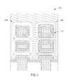
- FIG. 4depicts a gate-all-around device structure in accordance with some embodiments of the present disclosure.
- the inventive methodsmay advantageously be used provide multi-threshold voltage control in different device structures, including, for example, a complementary metal oxide semiconductor (CMOS) FinFet device, a planar CMOS device, and a Gate-All-Around (GAA) CMOS device.
- CMOScomplementary metal oxide semiconductor
- GAAGate-All-Around
- the inventive methodsmay facilitate one or more of increased process throughput by reducing the number of process steps (i.e. eliminating the need for an etch stop layer), reduced etch selectivity concerns, and more precise layer thickness control as compared to conventional processes.
- the inventive methodsmay allow thinner layers to be used to facilitate the further scaling down of the device structures (e.g., reduction in size).
- FIG. 1depicts a method 100 for forming a semiconductor device in accordance with some embodiments of the present disclosure. The method 100 is described below in accordance with the stages of fabrication of a semiconductor device (device 200 ) depicted in FIGS. 2A-2G .
- the method 100begins at 102 , by providing a substrate 202 , as depicted in FIG. 2A having a first layer 204 disposed thereon.
- the substrate 202may be any suitable substrate, such as a silicon substrate, a III-V compound substrate, a silicon germanium (SiGe) substrate, an epi-substrate, a silicon-on-insulator (SOI) substrate, a display substrate such as a liquid crystal display (LCD), a plasma display, an electro luminescence (EL) lamp display, a light emitting diode (LED) substrate, a solar cell array, solar panel, or the like.
- a silicon substratesuch as a silicon substrate, a III-V compound substrate, a silicon germanium (SiGe) substrate, an epi-substrate, a silicon-on-insulator (SOI) substrate, a display substrate such as a liquid crystal display (LCD), a plasma display, an electro luminescence (EL) lamp display, a light emitting diode (
- the substrate 202may be a semiconductor wafer (e.g., a 200 mm, 300 mm, or the like silicon wafer), such as a doped or undoped polysilicon wafer, a doped or undoped silicon wafer, a patterned or non-patterned wafer, or the like.
- the first layer 204may comprise an oxide layer.
- the substrate 202comprises a p-type conductivity well 206 and/or an n-type conductivity well 208 and respective source/drain regions 210 , 212 .
- a plurality of field isolation regionsmay be formed in the substrate 202 to isolate conductivity wells having different conductivity types (e.g., n-type or p-type) and/or to isolate adjacent transistors.
- the field isolation regionsmay be shallow trench isolation (STI) structures formed, for example, by etching a trench into the substrate 202 and then filling the trench with a suitable insulator, such as silicon oxide (oxide), silicon nitride (nitride), or the like.
- STIshallow trench isolation
- the first layer 204comprises a first feature 226 formed in the first layer 204 defining a first device 214 formed atop the p-type conductivity well 206 and a second feature 228 formed within the first layer 204 defining a second device 216 formed atop the n-type conductivity well 208 .
- the first feature 226 and second feature 228may be a trench or a via.
- the first feature 226 and second feature 228may have a height of about 100 nm and a width of about 5 nm to about 20 nm.
- the first and second devices 214 , 216each comprise a dielectric layer 218 , and a barrier layer 220 disposed atop the dielectric layer 218 .
- the dielectric layer 218may be formed from a single deposited layer that is subsequently patterned, or that is simultaneously deposited into a patterned region, to define the dielectric layer 218 .
- the dielectric layer 218may comprise a dielectric material having a dielectric constant of about 3.9.
- the dielectric layer 218may include one or more dielectric materials, such as at least one of silicon dioxide (SiO 2 ) silicon oxynitride (SiON), or other suitable dielectric materials.
- the dielectric layer 218may comprise a high-k material, such as a material having a dielectric constant greater than about 3.9.
- the high-K dielectric materialmay be hafnium oxide (HfO2), hafnium silicon oxide (HfSiOx), hafnium silicon oxynitride (HfSiNOx), or the like.
- the barrier layer 220may comprise for example tantalum nitride (TaN) or titanium nitride (TiN) having any suitable thickness for use in a device 200 , for example a thickness of up to about 40 angstroms.
- the first and second devices 214 , 216each comprise a polycrystalline material (not shown), for example polycrystalline silicon, disposed atop the barrier layer 220 .
- the polycrystalline materialis etched via any suitable etching process, such as a plasma etching process, to expose the upper surface of the barrier layer 220 , as shown in FIG. 2B .
- the polycrystalline materialmay be etched to expose the upper surface of the barrier layer 220 disposed atop the p-type conductivity well 206 and the upper surface of the barrier layer 220 disposed atop the n-type conductivity well 208 .
- the substrate 202may be exposed to a process gas comprising fluorine (F) or chlorine (Cl) to facilitate etching the polycrystalline material.
- a plasmamay be formed from the process gas. Ions from the plasma may be directed toward the substrate 202 to etch the polycrystalline material.
- a blocking layer 224is deposited atop the first and second feature 226 , 228 of the substrate 202 .
- the blocking layer 224has a thickness of about 1 nm to about 200 nm.
- the blocking layer 224may fill the first and second feature 226 , 228 .
- the blocking layer 224is composed of any material suitable for preventing or delaying the formation of a subsequently deposited work function layer thereon, as described at 108 below.
- the blocking layer 224is a carbon-containing layer.
- the carbon-containing layeris, for example, an amorphous carbon hard mask layer.
- the carbon-containing layermay be deposited via any process suitable to deposit a carbon-containing layer having the selected characteristics (e.g., composition, uniformity, or the like).
- the carbon-containing layermay be deposited via a spin-on coating process, a chemical vapor deposition (CVD) process, or an atomic layer deposition (ALD) process.
- exemplary spin on carbon films with a high decomposition temperature used in patterning and planarizationmay be used.
- An example of a suitable CVD deposited carbon filmincludes APFTM, from Applied Materials, Inc. of Santa Clara, Calif.
- the blocking layer 224is an oxygen-containing layer for example, a silicon oxide (SiO x ) layer or a silicon oxynitride (SiON) layer.
- the oxygen-containing layermay be deposited via any process suitable to deposit an oxygen-containing layer having the selected characteristics (e.g., composition, uniformity, or the like).
- the oxygen-containing layermay be deposited via a chemical vapor deposition or atomic layer deposition process.
- the blocking layer 224is a silicon (Si) layer, or a silicon nitride (SiN) layer, an aluminum nitride (AlN) layer, or the like.
- a portion of the blocking layer 224is selectively removed from atop the substrate to expose the first feature 226 .
- the blocking layer 224is a carbon-containing layer
- the blocking layermay be removed using conventional techniques to remove carbon-containing films from substrates, for example ashing techniques or etching techniques.
- the blocking layer 224may be etched using an suitable oxygen containing plasma (e.g., O 2 , CO 2 , or the like), a suitable hydrogen-containing plasma (e.g., H 2 , NH 3 , or the like), a suitable nitrogen-containing plasma (e.g., N 2 , NH 3 , or the like), combinations thereof (e.g., H 2 /N 2 , or the like), or the like.
- a patterned layersuch as a mask layer or anti-reflective coating (ARC) may be deposited atop the blocking layer 224 to create a pattern for selective etching.
- Such masking materialsmay include, for example, one or more of a photoresist, silicon nitride (Si 3 N 4 ), or silicon oxide (SiO 2 ).
- a first work function layer 230is selectively deposited atop the first feature 226 .
- the first work function layer 230may comprise any suitable metal, metal alloy or metal-containing material capable of functioning with the device 200 to produce a chosen threshold voltage of the device.
- Exemplary metals, metal alloys or metal-containing materials that may comprise the first work function layer 230may include one or more titanium nitride (TiN), titanium aluminum (TiAl), titanium aluminum carbide (TiAlC), tantalum aluminum (TaAl), tantalum nitride (TaN), tantalum aluminum carbide (TaAlC), tungsten (W), or cobalt (Co).
- the first work function layer 230has a thickness of about 0.5 nm to about 4 nm.
- the first work function layer 230is deposited via a CVD (Chemical Vapor Deposition) or an ALD (atomic layer deposition process).
- the substrate 202is exposed to a precursor gas that selectively deposits the first work function layer 230 atop the first portion of the substrate but not atop the blocking layer 224 .
- the precursor gasis a metal organic compound or metal inorganic compound with a vapor pressure of greater than about 0.1 mTorr at about 200 degrees Celsius and comprising one of, or at least one of, tungsten (W), molybdenum (Mo), niobium (Nb), cobalt (Co), nickel (Ni), vanadium (V), aluminum (Al), or ruthenium (Ru).
- the precursor gasis one of WCl 5 , Cp′ 2 WH 2 , Cp′W(CO) 3 H, Cp′W(CO) 2 NO, (RN) 2 (R′ 2 N) 2 W, WOCl 4 , Cp′ 2 MoH 2 , Cp′Mo(CO) 3 H, Cp′Mo(CO) 2 NO, (RN) 2 (R′ 2 N) 2 Mo, MoOCl 4 , (RN)(R′ 2 N) 3 Nb, NbCl 5 , Cp 2 NbH 3 , CpNb(CO) 4 H, Cp(allyl)Nb(CO), where R and R′ are each independently selected from H, alkyl (2-5) and where Cp′ is R 1 R 2 R 3 R 4 R 5 Cp where each R is independently selected from H, alkyl, alkene, or the like.
- suitable precursor gasesmay include cobalt carbonyl complexes, cobalt amidinate compounds, cobaltocene compounds (Co(C 5 H 5 ) 2 ), cobalt dienyl complexes, cobalt nitrosyl complexes, derivatives thereof, complexes thereof, plasmas thereof, or combinations thereof.
- dicobalt hexacarbonyl acetyl compoundsmay be used as a precursor to form a cobalt work function layer.
- a suitable precursor gasmay include tungsten hexafluoride (WF 6 ), tungsten hexachloride (WCl 6 ), tungsten carbonyl (W(CO) 6 ), bis(cyclopentadienyl)tungsten dichloride (Cp 2 WCl 2 ), mesitylene tungsten tricarbonyl (C 9 H 12 W(CO) 3 ), or derivatives thereof.
- WF 6tungsten hexafluoride
- WCl 6tungsten hexachloride
- W(CO) 6tungsten carbonyl
- Cp 2 WCl 2bis(cyclopentadienyl)tungsten dichloride
- mesitylene tungsten tricarbonylC 9 H 12 W(CO) 3
- a suitable precursor gasmay include nickel carbonyl complexes, nickel am idinate compounds, nickelocene compounds (Ni(C 5 H 5 ) 2 ), nickel dienyl complexes, nickel nitrosyl complexes, derivatives thereof, complexes thereof, plasmas thereof, or combinations thereof.
- a suitable precursor gasmay include ruthenium carbonyl complexes, ruthenium amidinate compounds, ruthenium ocene compounds (Ru(C 5 H 5 ) 2 ), ruthenium dienyl complexes, ruthenium nitrosyl complexes derivatives thereof, complexes thereof, plasmas thereof, or combinations thereof.
- ruthenium carbonyl complexesruthenium amidinate compounds
- ruthenium ocene compoundsRu(C 5 H 5 ) 2
- ruthenium dienyl complexesruthenium nitrosyl complexes derivatives thereof, complexes thereof, plasmas thereof, or combinations thereof.
- ruthenium nitrosyl complexes derivatives thereofcomplexes thereof, plasmas thereof, or combinations thereof.
- the blocking layer 224is removed to expose the second feature 228 .
- the blocking layermay be removed using conventional techniques to remove carbon-containing films from substrates, for example ashing techniques or etching techniques.
- the blocking layer 224may be etched using an oxygen containing plasma (e.g., O 2 , CO 2 , or the like), a hydrogen-containing plasma (e.g., H 2 , NH 3 , or the like), combinations thereof, or the like.
- an oxygen containing plasmae.g., O 2 , CO 2 , or the like
- a hydrogen-containing plasmae.g., H 2 , NH 3 , or the like
- a thin layer of the first work function layer 230may form atop the portion of the blocking layer 224 covering the second feature 228 .
- the portion of the first work function layer 230 formed atop the portion of the blocking layer 224 covering the second feature 228may be etched, for example using conventional plasma etching techniques, prior to etching the portion of the blocking layer 224 covering the second feature 228 .
- a second work function layer 232is deposited atop the first work function layer 230 and the second feature 228 .
- the second work function layer 232may comprise any suitable metal, metal alloy or metal-containing material capable of functioning with the device 200 to produce a chosen threshold voltage of the device.
- Exemplary metals, metal alloys or metal-containing materials that may comprise the first work function layer 230 or the second work function layer 232may include one or more titanium nitride (TiN), titanium aluminum (TiAl), titanium aluminum carbide (TiAlC), tantalum aluminum (TaAl), tantalum nitride (TaN), tantalum aluminum carbide (TaAlC), tungsten (W), or cobalt (Co).
- the second work function layer 232has a thickness of about 0.5 nm to about 4 nm, or about 0.5 nm to about 10 nm.
- the second work function layer 232is different from the first work function layer 230 (e.g., the first work function layer 230 may be TiN and the second work function layer may be TaAl).
- the second work function layer 232may be deposited via an atomic layer deposition process.
- the substrate 202may be exposed to a precursor gas selected to deposit the second work function layer 232 atop the first work function layer 230 and the second feature 228 of the first portion of the substrate 202 .
- the second precursor gasis a metal organic compound or metal inorganic compound with a vapor pressure of greater than about 0.1 mTorr at about 200 degrees Celsius and comprising one of, or at least one of, tungsten (W), molybdenum (Mo), niobium (Nb), cobalt (Co), nickel (Ni), vanadium (V), aluminum (Al), or ruthenium (Ru).
- the precursor gasis one of WCl5, Cp′ 2 WH 2 , Cp′W(CO) 3 H, Cp′W(CO) 2 NO, (RN) 2 (R′ 2 N) 2 W, WOCl 4 , Cp′ 2 MoH 2 , Cp′Mo(CO) 3 H, Cp′Mo(CO) 2 NO, (RN) 2 (R′ 2 N) 2 Mo, MoCl 4 , (RN)(R′ 2 N) 3 Nb, NbCl 5 , Cp 2 NbH 3 , CpNb(CO) 4 H, Cp(allyl)Nb(CO), where R and R′ are each independently selected from H, alkyl (2-5) and where Cp′ is R 1 R 2 R 3 R 4 R 5 Cp where each R is independently selected from H, alkyl, alkene, or the like.
- suitable precursor gasesmay include cobalt carbonyl complexes, cobalt amidinate compounds, cobaltocene compounds (Co(C 5 H 5 ) 2 ), cobalt dienyl complexes, cobalt nitrosyl complexes, derivatives thereof, complexes thereof, plasmas thereof, or combinations thereof.
- dicobalt hexacarbonyl acetyl compoundsmay be used as a precursor to form a cobalt work function layer.
- a suitable precursor gasmay include tungsten hexafluoride (WF 6 ), tungsten hexachloride (WCl 6 ), tungsten carbonyl (W(CO) 6 ), bis(cyclopentadienyl)tungsten dichloride (Cp 2 WCl 2 ), mesitylene tungsten tricarbonyl (C 9 H 12 W(CO) 3 ), or derivatives thereof.
- WF 6tungsten hexafluoride
- WCl 6tungsten hexachloride
- W(CO) 6tungsten carbonyl
- Cp 2 WCl 2bis(cyclopentadienyl)tungsten dichloride
- mesitylene tungsten tricarbonylC 9 H 12 W(CO) 3
- a suitable precursor gasmay include nickel carbonyl complexes, nickel am idinate compounds, nickelocene compounds (Ni(C 5 H 5 ) 2 ), nickel dienyl complexes, nickel nitrosyl complexes, derivatives thereof, complexes thereof, plasmas thereof, or combinations thereof.
- a suitable precursor gasmay include ruthenium carbonyl complexes, ruthenium amidinate compounds, ruthenium ocene compounds (Ru(C 5 H 5 ) 2 ), ruthenium dienyl complexes, ruthenium nitrosyl complexes derivatives thereof, complexes thereof, plasmas thereof, or combinations thereof.
- the precursor gasmay be a combination of a metal chloride, such as tungsten chloride (WCl 5 ) or tantalum chloride (TaCl), and a silicon containing gas, such as silane (SiH 4 ).
- the second work function layer 232has a thickness of about 0.5 nm to about 4 nm, or about 0.5 nm to about 10 nm. Additional work function layers may be also deposited to meet a selected threshold voltage of the device.
- a work function cap layer 234composed of for example TiN, may be deposited within the features 226 , 228 to prevent oxidation of the work function layers 230 , 232 .
- a fill layer 236may be deposited in the features 226 , 228 .
- the fill layermay be a conductive material, such as aluminum (Al), titanium aluminum (TiAl), cobalt aluminum (CoAl), tungsten (W) or the like.
- the final device 200is a planar FinFet structure.
- the method 100may be used to form a suitable Gate-All-Around (GAA) device structure known in the art, for example a Gate-All-Around (GAA) device structure 400 as depicted in FIG. 4 , having a first feature 402 and a second feature 404 , where the first feature 402 has a first selected work function metal layer 406 .
- GAAGate-All-Around
- FIG. 3depicts a cluster tool suitable for performing portions of the methods of the present disclosure.
- the cluster toolis a modular system comprising multiple chambers (e.g., process chambers 390 A-D, service chambers 391 A-B, or the like) which perform various functions including substrate cleaning, substrate center-finding and orientation, degassing, annealing, deposition and/or etching.
- the cluster toolmay include at least an etching apparatus and an atomic layer deposition or chemical vapor deposition apparatus configured to perform the method 100 of forming a multi-threshold voltage device as described above.
- the multiple chambers of the cluster toolare mounted to a central transfer chamber which houses a robot adapted to shuttle substrates between the chambers.
- the transfer chamberis typically maintained at a vacuum condition and provides an intermediate stage for shuttling substrates from one chamber to another and/or to a load lock chamber positioned at a front end of the cluster tool.
- the cluster tool 380generally comprises a plurality of chambers and robots and is preferably equipped with a microprocessor controller 381 programmed to carry out the various processing methods performed in the cluster tool 380 .
- a front-end environment 383is shown positioned in selective communication with a pair of load lock chambers 384 .
- a pod loader 385 disposed in the front-end environment 383is capable of linear and rotational movement (arrows 382 ) to shuttle cassettes of substrates between the load locks 384 and a plurality of pods 387 which are mounted on the front-end environment 383 .
- the load locks 384provide a first vacuum interface between the front-end environment 383 and a transfer chamber 388 .
- Two load locks 384are provided to increase throughput by alternatively communicating with the transfer chamber 388 and the front-end environment 383 .
- a robot 389is centrally disposed in the transfer chamber 388 to transfer substrates from the load locks 384 to one of the various processing chambers 390 A-D and service chambers 391 A-B.
- the method 100 of forming a multi-threshold voltage device as described abovemay be performed within one or more of the processing chambers 390 A-D.
- At least one of the processing chambers(for example, 390 A) may be an atomic layer deposition or chemical vapor deposition apparatus that performs a process on a substrate leading to deposition of the blocking layer 224 and/or the deposition of a work function layer 230 , 232 .
- At least one of the processing chambers(for example, 390 B) may be a plasma etch chamber that performs a process on a substrate leading to removal of some or all of the blocking layer 224 .
Landscapes
- Engineering & Computer Science (AREA)
- Physics & Mathematics (AREA)
- Electrodes Of Semiconductors (AREA)
- Computer Hardware Design (AREA)
- Condensed Matter Physics & Semiconductors (AREA)
- General Physics & Mathematics (AREA)
- Manufacturing & Machinery (AREA)
- Microelectronics & Electronic Packaging (AREA)
- Power Engineering (AREA)
- General Chemical & Material Sciences (AREA)
- Chemical Kinetics & Catalysis (AREA)
- Chemical & Material Sciences (AREA)
- Plasma & Fusion (AREA)
Abstract
Description
This application claims benefit of U.S. provisional patent application Ser. No. 61/953,332, filed Mar. 14, 2014, which is herein incorporated by reference in its entirety.
Embodiments of the present disclosure generally relate to methods of forming semiconductor devices.
Current complementary metal-oxide-semiconductor (CMOS) devices typically use metal gate materials to control transistor threshold voltage through the effective work function of a multi-layer metal stack. Different threshold voltages in a selected CMOS device may be achieved by changing the material and/or layer thickness of the metal gate stack to achieve the selected threshold voltage in each device. The current method of achieving multiple threshold voltages is a hybrid of selective well and halo implants and spatial control of the metal gate stack. While photo-patterning of well and halo implants is effective, continued fin width reduction is reducing the effectiveness of the well and halo implants, while the process remains intrinsically variable due to random dopant fluctuations. Spatial control of a metal gate stack can be achieved through a combination of photopatterning and etching in order to differentiate between n-type metal oxide semiconductor (NMOS) devices and p-type metal oxide semiconductor (PMOS) devices. However, the selective etching of the spatial control process uses an added etch stop layer, which consumes critical space in short gate length devices. Furthermore, the higher aspect ratio metal gate structures for future CMOS devices will utilize very high selectivity for removal of unwanted metal gate layers, which may render current methods impractical.
Accordingly, the inventors have developed improved methods of forming semiconductor devices.
Methods and apparatus for forming a multi-threshold voltage device on a substrate are provided herein. In some embodiments, a method of forming a multi-threshold voltage device includes: (a) providing a substrate having a first layer disposed thereon, wherein the substrate comprises a first feature and a second feature disposed within the first layer; (b) depositing a blocking layer atop the substrate; (c) selectively removing a portion of the blocking layer from atop the substrate to expose the first feature; (d) selectively depositing a first work function layer atop the first feature; (e) removing a remainder of the blocking layer to expose the second feature; and (f) depositing a second work function layer atop the first work function layer and the second feature.
In some embodiments, a method of forming a multi-threshold voltage device includes: (a) providing a substrate having a first layer disposed thereon, wherein the substrate comprises a first feature and a second feature disposed within the first layer; (b) depositing a carbon-containing layer atop the substrate via a spin-on process, wherein the carbon-containing layer has a thickness of about 5 to about 200 nm; (c) selectively removing a portion of the carbon-containing layer from atop the substrate to expose the first feature; (d) selectively depositing a first work function layer atop the first feature via an atomic layer deposition process, wherein the first work function layer has a thickness of about 0.5 nm to about 4 nm; (e) removing a remainder of the carbon-containing layer to expose the second feature; and (f) depositing a second work function layer atop the first work function layer and the second feature via an atomic layer deposition process, wherein the second work function layer has a thickness of about 0.5 nm to about 4 nm.
In some embodiments, a computer readable medium is provided having instructions stored thereon that, when executed, cause a method to be performed for forming a multi-threshold voltage device. The method may include any of the embodiments disclosed herein.
Other and further embodiments of the present disclosure are described below.
Embodiments of the present disclosure, briefly summarized above and discussed in greater detail below, can be understood by reference to the illustrative embodiments of the disclosure depicted in the appended drawings. It is to be noted, however, that the appended drawings illustrate only typical embodiments of this disclosure and are therefore not to be considered limiting of its scope, for the disclosure may admit to other equally effective embodiments.
To facilitate understanding, identical reference numerals have been used, where possible, to designate identical elements that are common to the figures. The figures are not drawn to scale and may be simplified for clarity. It is contemplated that elements and features of one embodiment may be beneficially incorporated in other embodiments without further recitation.
Methods for forming semiconductor devices on substrates are disclosed herein. In some embodiments, the inventive methods may advantageously be used provide multi-threshold voltage control in different device structures, including, for example, a complementary metal oxide semiconductor (CMOS) FinFet device, a planar CMOS device, and a Gate-All-Around (GAA) CMOS device. In some embodiments, the inventive methods may facilitate one or more of increased process throughput by reducing the number of process steps (i.e. eliminating the need for an etch stop layer), reduced etch selectivity concerns, and more precise layer thickness control as compared to conventional processes. In addition, the inventive methods may allow thinner layers to be used to facilitate the further scaling down of the device structures (e.g., reduction in size).
Themethod 100 begins at102, by providing asubstrate 202, as depicted inFIG. 2A having afirst layer 204 disposed thereon. Thesubstrate 202 may be any suitable substrate, such as a silicon substrate, a III-V compound substrate, a silicon germanium (SiGe) substrate, an epi-substrate, a silicon-on-insulator (SOI) substrate, a display substrate such as a liquid crystal display (LCD), a plasma display, an electro luminescence (EL) lamp display, a light emitting diode (LED) substrate, a solar cell array, solar panel, or the like. In some embodiments, thesubstrate 202 may be a semiconductor wafer (e.g., a 200 mm, 300 mm, or the like silicon wafer), such as a doped or undoped polysilicon wafer, a doped or undoped silicon wafer, a patterned or non-patterned wafer, or the like. In some embodiments, thefirst layer 204 may comprise an oxide layer. In some embodiments, thesubstrate 202 comprises a p-type conductivity well206 and/or an n-type conductivity well208 and respective source/drain regions
In some embodiments, such as where one or more devices are to be formed on thesubstrate 202, a plurality of field isolation regions (not shown) may be formed in thesubstrate 202 to isolate conductivity wells having different conductivity types (e.g., n-type or p-type) and/or to isolate adjacent transistors. The field isolation regions may be shallow trench isolation (STI) structures formed, for example, by etching a trench into thesubstrate 202 and then filling the trench with a suitable insulator, such as silicon oxide (oxide), silicon nitride (nitride), or the like.
Thefirst layer 204 comprises afirst feature 226 formed in thefirst layer 204 defining afirst device 214 formed atop the p-type conductivity well206 and asecond feature 228 formed within thefirst layer 204 defining asecond device 216 formed atop the n-type conductivity well208. In some embodiments, thefirst feature 226 andsecond feature 228 may be a trench or a via. In some embodiments, thefirst feature 226 andsecond feature 228 may have a height of about 100 nm and a width of about 5 nm to about 20 nm. In some embodiments, the first andsecond devices dielectric layer 218, and abarrier layer 220 disposed atop thedielectric layer 218.
In some embodiments, thedielectric layer 218 may be formed from a single deposited layer that is subsequently patterned, or that is simultaneously deposited into a patterned region, to define thedielectric layer 218. In some embodiments, thedielectric layer 218 may comprise a dielectric material having a dielectric constant of about 3.9. In some embodiments, thedielectric layer 218 may include one or more dielectric materials, such as at least one of silicon dioxide (SiO2) silicon oxynitride (SiON), or other suitable dielectric materials. In some embodiments thedielectric layer 218 may comprise a high-k material, such as a material having a dielectric constant greater than about 3.9. For example, the high-K dielectric material may be hafnium oxide (HfO2), hafnium silicon oxide (HfSiOx), hafnium silicon oxynitride (HfSiNOx), or the like.
In some embodiments, thebarrier layer 220 may comprise for example tantalum nitride (TaN) or titanium nitride (TiN) having any suitable thickness for use in adevice 200, for example a thickness of up to about 40 angstroms. In some embodiments, the first andsecond devices barrier layer 220. The polycrystalline material is etched via any suitable etching process, such as a plasma etching process, to expose the upper surface of thebarrier layer 220, as shown inFIG. 2B . The polycrystalline material may be etched to expose the upper surface of thebarrier layer 220 disposed atop the p-type conductivity well206 and the upper surface of thebarrier layer 220 disposed atop the n-type conductivity well208.
In some embodiments, thesubstrate 202 may be exposed to a process gas comprising fluorine (F) or chlorine (Cl) to facilitate etching the polycrystalline material. In some embodiments, a plasma may be formed from the process gas. Ions from the plasma may be directed toward thesubstrate 202 to etch the polycrystalline material.
At104, and as depicted inFIG. 2B , ablocking layer 224 is deposited atop the first andsecond feature substrate 202. In some embodiments, theblocking layer 224 has a thickness of about 1 nm to about 200 nm. In some embodiments, theblocking layer 224 may fill the first andsecond feature blocking layer 224 is composed of any material suitable for preventing or delaying the formation of a subsequently deposited work function layer thereon, as described at108 below. In some embodiments, theblocking layer 224 is a carbon-containing layer. In some embodiments, the carbon-containing layer is, for example, an amorphous carbon hard mask layer. The carbon-containing layer may be deposited via any process suitable to deposit a carbon-containing layer having the selected characteristics (e.g., composition, uniformity, or the like). For example, the carbon-containing layer may be deposited via a spin-on coating process, a chemical vapor deposition (CVD) process, or an atomic layer deposition (ALD) process. Exemplary spin on carbon films with a high decomposition temperature used in patterning and planarization may be used. An example of a suitable CVD deposited carbon film includes APF™, from Applied Materials, Inc. of Santa Clara, Calif. Alternatively, in some embodiments, theblocking layer 224 is an oxygen-containing layer for example, a silicon oxide (SiOx) layer or a silicon oxynitride (SiON) layer. The oxygen-containing layer may be deposited via any process suitable to deposit an oxygen-containing layer having the selected characteristics (e.g., composition, uniformity, or the like). For example, the oxygen-containing layer may be deposited via a chemical vapor deposition or atomic layer deposition process. In some embodiments, theblocking layer 224 is a silicon (Si) layer, or a silicon nitride (SiN) layer, an aluminum nitride (AlN) layer, or the like.
At106, and as depicted inFIG. 2C , a portion of theblocking layer 224 is selectively removed from atop the substrate to expose thefirst feature 226. In embodiments, where theblocking layer 224 is a carbon-containing layer, the blocking layer may be removed using conventional techniques to remove carbon-containing films from substrates, for example ashing techniques or etching techniques. In some embodiments, theblocking layer 224 may be etched using an suitable oxygen containing plasma (e.g., O2, CO2, or the like), a suitable hydrogen-containing plasma (e.g., H2, NH3, or the like), a suitable nitrogen-containing plasma (e.g., N2, NH3, or the like), combinations thereof (e.g., H2/N2, or the like), or the like. In some embodiments a patterned layer such as a mask layer or anti-reflective coating (ARC) may be deposited atop theblocking layer 224 to create a pattern for selective etching. Such masking materials may include, for example, one or more of a photoresist, silicon nitride (Si3N4), or silicon oxide (SiO2).
At108, as depicted inFIG. 2D , a firstwork function layer 230 is selectively deposited atop thefirst feature 226. The firstwork function layer 230 may comprise any suitable metal, metal alloy or metal-containing material capable of functioning with thedevice 200 to produce a chosen threshold voltage of the device. Exemplary metals, metal alloys or metal-containing materials that may comprise the firstwork function layer 230 may include one or more titanium nitride (TiN), titanium aluminum (TiAl), titanium aluminum carbide (TiAlC), tantalum aluminum (TaAl), tantalum nitride (TaN), tantalum aluminum carbide (TaAlC), tungsten (W), or cobalt (Co). In some embodiments, the firstwork function layer 230 has a thickness of about 0.5 nm to about 4 nm.
In some embodiments, the firstwork function layer 230 is deposited via a CVD (Chemical Vapor Deposition) or an ALD (atomic layer deposition process). Thesubstrate 202 is exposed to a precursor gas that selectively deposits the firstwork function layer 230 atop the first portion of the substrate but not atop theblocking layer 224. In some embodiments, the precursor gas is a metal organic compound or metal inorganic compound with a vapor pressure of greater than about 0.1 mTorr at about 200 degrees Celsius and comprising one of, or at least one of, tungsten (W), molybdenum (Mo), niobium (Nb), cobalt (Co), nickel (Ni), vanadium (V), aluminum (Al), or ruthenium (Ru). For example, in some embodiments, the precursor gas is one of WCl5, Cp′2WH2, Cp′W(CO)3H, Cp′W(CO)2NO, (RN)2(R′2N)2W, WOCl4, Cp′2MoH2, Cp′Mo(CO)3H, Cp′Mo(CO)2NO, (RN)2(R′2N)2Mo, MoOCl4, (RN)(R′2N)3Nb, NbCl5, Cp2NbH3, CpNb(CO)4H, Cp(allyl)Nb(CO), where R and R′ are each independently selected from H, alkyl (2-5) and where Cp′ is R1R2R3R4R5Cp where each R is independently selected from H, alkyl, alkene, or the like. For example, in some embodiments, where the first work function layer is cobalt, suitable precursor gases may include cobalt carbonyl complexes, cobalt amidinate compounds, cobaltocene compounds (Co(C5H5)2), cobalt dienyl complexes, cobalt nitrosyl complexes, derivatives thereof, complexes thereof, plasmas thereof, or combinations thereof. For example, in some embodiments, dicobalt hexacarbonyl acetyl compounds may be used as a precursor to form a cobalt work function layer. Alternatively, in some embodiments where the first work function layer is tungsten a suitable precursor gas may include tungsten hexafluoride (WF6), tungsten hexachloride (WCl6), tungsten carbonyl (W(CO)6), bis(cyclopentadienyl)tungsten dichloride (Cp2WCl2), mesitylene tungsten tricarbonyl (C9H12W(CO)3), or derivatives thereof. Alternatively, in some embodiments where the first work function layer is nickel a suitable precursor gas may include nickel carbonyl complexes, nickel am idinate compounds, nickelocene compounds (Ni(C5H5)2), nickel dienyl complexes, nickel nitrosyl complexes, derivatives thereof, complexes thereof, plasmas thereof, or combinations thereof. Alternatively, in some embodiments where the first work function layer is ruthenium a suitable precursor gas may include ruthenium carbonyl complexes, ruthenium amidinate compounds, ruthenium ocene compounds (Ru(C5H5)2), ruthenium dienyl complexes, ruthenium nitrosyl complexes derivatives thereof, complexes thereof, plasmas thereof, or combinations thereof. In some embodiments, for example when depositing a work function layer using a chloride precursor, the addition of a hydrogen chloride gas can inhibit deposition of the work function layer atop the blocking layer.
At110, as depicted inFIG. 2E , the remainder of theblocking layer 224 is removed to expose thesecond feature 228. As described above, the blocking layer may be removed using conventional techniques to remove carbon-containing films from substrates, for example ashing techniques or etching techniques. In some embodiments, theblocking layer 224 may be etched using an oxygen containing plasma (e.g., O2, CO2, or the like), a hydrogen-containing plasma (e.g., H2, NH3, or the like), combinations thereof, or the like. In some embodiments, during deposition of the firstwork function layer 230 at108, a thin layer of the firstwork function layer 230 may form atop the portion of theblocking layer 224 covering thesecond feature 228. In such embodiments, the portion of the firstwork function layer 230 formed atop the portion of theblocking layer 224 covering thesecond feature 228 may be etched, for example using conventional plasma etching techniques, prior to etching the portion of theblocking layer 224 covering thesecond feature 228.
At112, and as depicted inFIG. 2F , a secondwork function layer 232 is deposited atop the firstwork function layer 230 and thesecond feature 228. The secondwork function layer 232 may comprise any suitable metal, metal alloy or metal-containing material capable of functioning with thedevice 200 to produce a chosen threshold voltage of the device. Exemplary metals, metal alloys or metal-containing materials that may comprise the firstwork function layer 230 or the secondwork function layer 232 may include one or more titanium nitride (TiN), titanium aluminum (TiAl), titanium aluminum carbide (TiAlC), tantalum aluminum (TaAl), tantalum nitride (TaN), tantalum aluminum carbide (TaAlC), tungsten (W), or cobalt (Co). In some embodiments, the secondwork function layer 232 has a thickness of about 0.5 nm to about 4 nm, or about 0.5 nm to about 10 nm. The secondwork function layer 232 is different from the first work function layer230 (e.g., the firstwork function layer 230 may be TiN and the second work function layer may be TaAl).
In some embodiments, the secondwork function layer 232 may be deposited via an atomic layer deposition process. For example, thesubstrate 202 may be exposed to a precursor gas selected to deposit the secondwork function layer 232 atop the firstwork function layer 230 and thesecond feature 228 of the first portion of thesubstrate 202. In some embodiments, the second precursor gas is a metal organic compound or metal inorganic compound with a vapor pressure of greater than about 0.1 mTorr at about 200 degrees Celsius and comprising one of, or at least one of, tungsten (W), molybdenum (Mo), niobium (Nb), cobalt (Co), nickel (Ni), vanadium (V), aluminum (Al), or ruthenium (Ru). For example, in some embodiments, the precursor gas is one of WCl5, Cp′2WH2, Cp′W(CO)3H, Cp′W(CO)2NO, (RN)2(R′2N)2W, WOCl4, Cp′2MoH2, Cp′Mo(CO)3H, Cp′Mo(CO)2NO, (RN)2(R′2N)2Mo, MoCl4, (RN)(R′2N)3Nb, NbCl5, Cp2NbH3, CpNb(CO)4H, Cp(allyl)Nb(CO), where R and R′ are each independently selected from H, alkyl (2-5) and where Cp′ is R1R2R3R4R5Cp where each R is independently selected from H, alkyl, alkene, or the like. For example, where the secondwork function layer 232 is cobalt, suitable precursor gases may include cobalt carbonyl complexes, cobalt amidinate compounds, cobaltocene compounds (Co(C5H5)2), cobalt dienyl complexes, cobalt nitrosyl complexes, derivatives thereof, complexes thereof, plasmas thereof, or combinations thereof. For example, in some embodiments, dicobalt hexacarbonyl acetyl compounds may be used as a precursor to form a cobalt work function layer. Alternatively, where the secondwork function layer 232 is tungsten a suitable precursor gas may include tungsten hexafluoride (WF6), tungsten hexachloride (WCl6), tungsten carbonyl (W(CO)6), bis(cyclopentadienyl)tungsten dichloride (Cp2WCl2), mesitylene tungsten tricarbonyl (C9H12W(CO)3), or derivatives thereof. Alternatively, in some embodiments where the second work function layer is nickel a suitable precursor gas may include nickel carbonyl complexes, nickel am idinate compounds, nickelocene compounds (Ni(C5H5)2), nickel dienyl complexes, nickel nitrosyl complexes, derivatives thereof, complexes thereof, plasmas thereof, or combinations thereof. Alternatively, in some embodiments where the second work function layer is ruthenium a suitable precursor gas may include ruthenium carbonyl complexes, ruthenium amidinate compounds, ruthenium ocene compounds (Ru(C5H5)2), ruthenium dienyl complexes, ruthenium nitrosyl complexes derivatives thereof, complexes thereof, plasmas thereof, or combinations thereof. In some embodiments, the precursor gas may be a combination of a metal chloride, such as tungsten chloride (WCl5) or tantalum chloride (TaCl), and a silicon containing gas, such as silane (SiH4). In some embodiments, the secondwork function layer 232 has a thickness of about 0.5 nm to about 4 nm, or about 0.5 nm to about 10 nm. Additional work function layers may be also deposited to meet a selected threshold voltage of the device.
104 to110 ofmethod 100 may be repeated as necessary to obtain a first selected work function in the first feature and a second selected work function in the second feature. Following formation of the work function layers230,232 having the selected work functions, additional layers may deposited as necessary within thefeatures device 200. For example, as depicted inFIG. 2G , a workfunction cap layer 234, composed of for example TiN, may be deposited within thefeatures fill layer 236 may be deposited in thefeatures
In some embodiments, thefinal device 200, as depicted inFIG. 2G is a planar FinFet structure. In some embodiments, themethod 100 may be used to form a suitable Gate-All-Around (GAA) device structure known in the art, for example a Gate-All-Around (GAA)device structure 400 as depicted inFIG. 4 , having afirst feature 402 and asecond feature 404, where thefirst feature 402 has a first selected workfunction metal layer 406.
By way of illustration, aparticular cluster tool 380 is shown in a plan view inFIG. 3 . Thecluster tool 380 generally comprises a plurality of chambers and robots and is preferably equipped with amicroprocessor controller 381 programmed to carry out the various processing methods performed in thecluster tool 380. A front-end environment 383 is shown positioned in selective communication with a pair ofload lock chambers 384. Apod loader 385 disposed in the front-end environment 383 is capable of linear and rotational movement (arrows382) to shuttle cassettes of substrates between the load locks384 and a plurality ofpods 387 which are mounted on the front-end environment 383. The load locks384 provide a first vacuum interface between the front-end environment 383 and atransfer chamber 388. Twoload locks 384 are provided to increase throughput by alternatively communicating with thetransfer chamber 388 and the front-end environment 383. Thus, while oneload lock 384 communicates with thetransfer chamber 388, asecond load lock 384 communicates with the front-end environment 383. Arobot 389 is centrally disposed in thetransfer chamber 388 to transfer substrates from the load locks384 to one of thevarious processing chambers 390A-D andservice chambers 391A-B.
In some embodiments, themethod 100 of forming a multi-threshold voltage device as described above may be performed within one or more of theprocessing chambers 390A-D. At least one of the processing chambers (for example,390A) may be an atomic layer deposition or chemical vapor deposition apparatus that performs a process on a substrate leading to deposition of theblocking layer 224 and/or the deposition of awork function layer blocking layer 224.
While the foregoing is directed to embodiments of the present disclosure, other and further embodiments may be devised without departing from the basic scope thereof.
Claims (20)
1. A method of forming a multi-threshold voltage device, comprising:
(a) providing a substrate having a first layer disposed thereon, wherein the substrate comprises a first feature and a second feature disposed within the first layer;
(b) depositing a blocking layer atop the substrate, the first feature, and the second feature;
(c) selectively removing a portion of the blocking layer from atop the substrate to expose the first feature;
(d) subsequently, selectively depositing a first work function layer atop the first feature but not atop a remainder of the blocking layer;
(e) removing the remainder of the blocking layer to expose the second feature; and
(f) depositing a second work function layer atop the first work function layer and the second feature.
2. The method ofclaim 1 , wherein the blocking layer is one of a carbon-containing layer or an oxygen-containing layer.
3. The method ofclaim 2 , wherein the carbon-containing layer is an amorphous carbon hard mask layer.
4. The method ofclaim 2 , wherein the carbon-containing layer is deposited via one of a spin-on coating process, chemical vapor deposition process, or atomic layer deposition process.
5. The method ofclaim 1 , wherein the blocking layer has a thickness of about 5 to about 200 nm.
6. The method ofclaim 1 , wherein the first work function layer has a thickness of about 0.5 nm to about 10 nm, and wherein the second work function layer has a thickness of about 0.5 nm to about 10 nm.
7. The method ofclaim 1 , wherein removing a portion of the blocking layer further comprises patterning the blocking layer using a plasma formed from one of an oxygen containing gas or a hydrogen containing gas.
8. The method ofclaim 1 , further comprising depositing the first work function layer via an atomic layer deposition process.
9. The method ofclaim 8 , further comprising exposing the substrate to one or more precursor gases to selectively deposit the first work function layer atop the first feature.
10. The method ofclaim 9 , further comprising exposing the blocking layer to a first gas that delays formation of the first work function layer atop the blocking layer.
11. The method ofclaim 10 , wherein the first gas is hydrogen chloride.
12. The method ofclaim 9 , wherein the precursor gas comprises one of tungsten, molybdenum, niobium, cobalt, nickel, vanadium, aluminum, or ruthenium.
13. The method ofclaim 1 , wherein depositing the second work function layer further comprises exposing the substrate to a second precursor gas.
14. The method ofclaim 13 , wherein the second precursor gas comprises one of tungsten, molybdenum, niobium, cobalt, nickel, vanadium, aluminum, or ruthenium.
15. The method ofclaim 1 , repeating (b)-(f) to obtain a first selected work function in the first feature and a second selected work function in the second feature.
16. The method ofclaim 1 , wherein the first feature and second feature are each formed atop a first conductivity well and a second conductivity well.
17. A method of forming a multi-threshold voltage device, comprising:
(a) providing a substrate having a first layer disposed thereon, wherein the substrate comprises a first feature and a second feature disposed within the first layer;
(b) depositing one of a carbon-containing layer or an oxygen-containing layer atop the substrate, the first feature, and the second feature, wherein the carbon-containing layer or the oxygen-containing layer has a thickness of about 1 to about 200 nm;
(c) selectively removing a portion of the carbon-containing layer or oxygen-containing layer from atop the substrate to expose the first feature;
(d) selectively depositing a first work function layer atop the first feature, but not atop a remainder of the carbon-containing layer or oxygen-containing layer, via an atomic layer deposition process, wherein the first work function layer has a thickness of about 0.5 nm to about 4 nm;
(e) removing the remainder of the carbon-containing layer or oxygen-containing layer to expose the second feature; and
(f) depositing a second work function layer atop the first work function layer and the second feature via an atomic layer deposition process, wherein the second work function layer has a thickness of about 0.5 nm to about 4 nm.
18. The method ofclaim 1 , wherein the second work function layer is deposited directly atop the first work function layer and the second feature.
19. The method ofclaim 17 , wherein the second work function layer is deposited directly atop the first work function layer and the second feature.
20. A non-transitory computer readable medium having instructions stored thereon that, when executed, cause a method for forming a multi-threshold voltage device, the method comprising:
(a) providing a substrate having a first layer disposed thereon, wherein the substrate comprises a first feature and a second feature disposed within the first layer;
(b) depositing a blocking layer atop the substrate, the first feature, and the second feature;
(c) selectively removing a portion of the blocking layer from atop the substrate to expose the first feature;
(d) subsequently, selectively depositing a first work function layer atop the first feature but not atop a remainder of the blocking layer;
(e) removing the remainder of the blocking layer to expose the second feature; and
(f) depositing a second work function layer atop the first work function layer and the second feature.
Priority Applications (3)
| Application Number | Priority Date | Filing Date | Title |
|---|---|---|---|
| US14/627,861US10109534B2 (en) | 2014-03-14 | 2015-02-20 | Multi-threshold voltage (Vt) workfunction metal by selective atomic layer deposition (ALD) |
| TW104105892ATWI663640B (en) | 2014-03-14 | 2015-02-24 | Multi-threshold voltage (vt) workfunction metal by selective atomic layer deposition (ald) |
| PCT/US2015/018262WO2015138176A1 (en) | 2014-03-14 | 2015-03-02 | MULTI-THRESHOLD VOLTAGE (Vt) WORKFUNCTION METAL BY SELECTIVE ATOMIC LAYER DEPOSITION (ALD) |
Applications Claiming Priority (2)
| Application Number | Priority Date | Filing Date | Title |
|---|---|---|---|
| US201461953332P | 2014-03-14 | 2014-03-14 | |
| US14/627,861US10109534B2 (en) | 2014-03-14 | 2015-02-20 | Multi-threshold voltage (Vt) workfunction metal by selective atomic layer deposition (ALD) |
Publications (2)
| Publication Number | Publication Date |
|---|---|
| US20150262828A1 US20150262828A1 (en) | 2015-09-17 |
| US10109534B2true US10109534B2 (en) | 2018-10-23 |
Family
ID=54069635
Family Applications (1)
| Application Number | Title | Priority Date | Filing Date |
|---|---|---|---|
| US14/627,861Expired - Fee RelatedUS10109534B2 (en) | 2014-03-14 | 2015-02-20 | Multi-threshold voltage (Vt) workfunction metal by selective atomic layer deposition (ALD) |
Country Status (3)
| Country | Link |
|---|---|
| US (1) | US10109534B2 (en) |
| TW (1) | TWI663640B (en) |
| WO (1) | WO2015138176A1 (en) |
Cited By (4)
| Publication number | Priority date | Publication date | Assignee | Title |
|---|---|---|---|---|
| US20210126018A1 (en)* | 2018-04-06 | 2021-04-29 | International Business Machines Corporation | Gate stack quality for gate-all-around field-effect transistors |
| US11075276B2 (en) | 2018-10-08 | 2021-07-27 | Applied Materials, Inc. | Methods and apparatus for n-type metal oxide semiconductor (NMOS) metal gate materials using atomic layer deposition (ALD) processes with metal based precursors |
| US12068387B2 (en) | 2021-10-19 | 2024-08-20 | International Business Machines Corporation | Multiple threshold voltage scheme in complementary metal oxide semiconductor transistors |
| US12119228B2 (en) | 2018-01-19 | 2024-10-15 | Asm Ip Holding B.V. | Deposition method |
Families Citing this family (359)
| Publication number | Priority date | Publication date | Assignee | Title |
|---|---|---|---|---|
| US9394608B2 (en) | 2009-04-06 | 2016-07-19 | Asm America, Inc. | Semiconductor processing reactor and components thereof |
| US8802201B2 (en) | 2009-08-14 | 2014-08-12 | Asm America, Inc. | Systems and methods for thin-film deposition of metal oxides using excited nitrogen-oxygen species |
| US9312155B2 (en) | 2011-06-06 | 2016-04-12 | Asm Japan K.K. | High-throughput semiconductor-processing apparatus equipped with multiple dual-chamber modules |
| US10854498B2 (en) | 2011-07-15 | 2020-12-01 | Asm Ip Holding B.V. | Wafer-supporting device and method for producing same |
| US20130023129A1 (en) | 2011-07-20 | 2013-01-24 | Asm America, Inc. | Pressure transmitter for a semiconductor processing environment |
| US9017481B1 (en) | 2011-10-28 | 2015-04-28 | Asm America, Inc. | Process feed management for semiconductor substrate processing |
| US10714315B2 (en) | 2012-10-12 | 2020-07-14 | Asm Ip Holdings B.V. | Semiconductor reaction chamber showerhead |
| US20160376700A1 (en) | 2013-02-01 | 2016-12-29 | Asm Ip Holding B.V. | System for treatment of deposition reactor |
| US9637819B2 (en) | 2013-11-18 | 2017-05-02 | Applied Materials, Inc. | Methods for preferential growth of cobalt within substrate features |
| US10683571B2 (en) | 2014-02-25 | 2020-06-16 | Asm Ip Holding B.V. | Gas supply manifold and method of supplying gases to chamber using same |
| US10167557B2 (en) | 2014-03-18 | 2019-01-01 | Asm Ip Holding B.V. | Gas distribution system, reactor including the system, and methods of using the same |
| US11015245B2 (en) | 2014-03-19 | 2021-05-25 | Asm Ip Holding B.V. | Gas-phase reactor and system having exhaust plenum and components thereof |
| US10858737B2 (en) | 2014-07-28 | 2020-12-08 | Asm Ip Holding B.V. | Showerhead assembly and components thereof |
| US10094023B2 (en) | 2014-08-01 | 2018-10-09 | Applied Materials, Inc. | Methods and apparatus for chemical vapor deposition of a cobalt layer |
| US9890456B2 (en) | 2014-08-21 | 2018-02-13 | Asm Ip Holding B.V. | Method and system for in situ formation of gas-phase compounds |
| US10941490B2 (en) | 2014-10-07 | 2021-03-09 | Asm Ip Holding B.V. | Multiple temperature range susceptor, assembly, reactor and system including the susceptor, and methods of using the same |
| US9657845B2 (en) | 2014-10-07 | 2017-05-23 | Asm Ip Holding B.V. | Variable conductance gas distribution apparatus and method |
| US10043709B2 (en) | 2014-11-07 | 2018-08-07 | Applied Materials, Inc. | Methods for thermally forming a selective cobalt layer |
| US10276355B2 (en) | 2015-03-12 | 2019-04-30 | Asm Ip Holding B.V. | Multi-zone reactor, system including the reactor, and method of using the same |
| US10458018B2 (en)* | 2015-06-26 | 2019-10-29 | Asm Ip Holding B.V. | Structures including metal carbide material, devices including the structures, and methods of forming same |
| US10600673B2 (en) | 2015-07-07 | 2020-03-24 | Asm Ip Holding B.V. | Magnetic susceptor to baseplate seal |
| US10211308B2 (en) | 2015-10-21 | 2019-02-19 | Asm Ip Holding B.V. | NbMC layers |
| US9583486B1 (en)* | 2015-11-19 | 2017-02-28 | International Business Machines Corporation | Stable work function for narrow-pitch devices |
| KR102434993B1 (en) | 2015-12-09 | 2022-08-24 | 삼성전자주식회사 | Semiconductor device |
| US11139308B2 (en) | 2015-12-29 | 2021-10-05 | Asm Ip Holding B.V. | Atomic layer deposition of III-V compounds to form V-NAND devices |
| US9859169B2 (en) | 2016-01-15 | 2018-01-02 | International Business Machines Corporation | Field effect transistor stack with tunable work function |
| US9583400B1 (en) | 2016-01-15 | 2017-02-28 | International Business Machines Corporation | Gate stack with tunable work function |
| US9559016B1 (en) | 2016-01-15 | 2017-01-31 | International Business Machines Corporation | Semiconductor device having a gate stack with tunable work function |
| US10079182B2 (en) | 2016-01-15 | 2018-09-18 | International Business Machines Corporation | Field effect transistor gate stack |
| US10529554B2 (en) | 2016-02-19 | 2020-01-07 | Asm Ip Holding B.V. | Method for forming silicon nitride film selectively on sidewalls or flat surfaces of trenches |
| US10343920B2 (en) | 2016-03-18 | 2019-07-09 | Asm Ip Holding B.V. | Aligned carbon nanotubes |
| US10249501B2 (en) | 2016-03-28 | 2019-04-02 | International Business Machines Corporation | Single process for liner and metal fill |
| US10190213B2 (en) | 2016-04-21 | 2019-01-29 | Asm Ip Holding B.V. | Deposition of metal borides |
| US10865475B2 (en) | 2016-04-21 | 2020-12-15 | Asm Ip Holding B.V. | Deposition of metal borides and silicides |
| US10367080B2 (en) | 2016-05-02 | 2019-07-30 | Asm Ip Holding B.V. | Method of forming a germanium oxynitride film |
| US10032628B2 (en) | 2016-05-02 | 2018-07-24 | Asm Ip Holding B.V. | Source/drain performance through conformal solid state doping |
| US11453943B2 (en) | 2016-05-25 | 2022-09-27 | Asm Ip Holding B.V. | Method for forming carbon-containing silicon/metal oxide or nitride film by ALD using silicon precursor and hydrocarbon precursor |
| US9859151B1 (en) | 2016-07-08 | 2018-01-02 | Asm Ip Holding B.V. | Selective film deposition method to form air gaps |
| US10612137B2 (en) | 2016-07-08 | 2020-04-07 | Asm Ip Holdings B.V. | Organic reactants for atomic layer deposition |
| JP6793243B2 (en)* | 2016-07-14 | 2020-12-02 | インテグリス・インコーポレーテッド | CVD Mo deposition by using MoOCl4 |
| US10714385B2 (en) | 2016-07-19 | 2020-07-14 | Asm Ip Holding B.V. | Selective deposition of tungsten |
| KR102532607B1 (en) | 2016-07-28 | 2023-05-15 | 에이에스엠 아이피 홀딩 비.브이. | Substrate processing apparatus and method of operating the same |
| US9887082B1 (en) | 2016-07-28 | 2018-02-06 | Asm Ip Holding B.V. | Method and apparatus for filling a gap |
| US9812320B1 (en) | 2016-07-28 | 2017-11-07 | Asm Ip Holding B.V. | Method and apparatus for filling a gap |
| US10026652B2 (en) | 2016-08-17 | 2018-07-17 | Samsung Electronics Co., Ltd. | Horizontal nanosheet FETs and method of manufacturing the same |
| US9947594B2 (en)* | 2016-09-19 | 2018-04-17 | Taiwan Semiconductor Manufacturing Co., Ltd. | Semiconductor device and manufacturing method thereof |
| US10643826B2 (en) | 2016-10-26 | 2020-05-05 | Asm Ip Holdings B.V. | Methods for thermally calibrating reaction chambers |
| US11532757B2 (en) | 2016-10-27 | 2022-12-20 | Asm Ip Holding B.V. | Deposition of charge trapping layers |
| US10714350B2 (en) | 2016-11-01 | 2020-07-14 | ASM IP Holdings, B.V. | Methods for forming a transition metal niobium nitride film on a substrate by atomic layer deposition and related semiconductor device structures |
| US10229833B2 (en) | 2016-11-01 | 2019-03-12 | Asm Ip Holding B.V. | Methods for forming a transition metal nitride film on a substrate by atomic layer deposition and related semiconductor device structures |
| US10643904B2 (en) | 2016-11-01 | 2020-05-05 | Asm Ip Holdings B.V. | Methods for forming a semiconductor device and related semiconductor device structures |
| US10134757B2 (en) | 2016-11-07 | 2018-11-20 | Asm Ip Holding B.V. | Method of processing a substrate and a device manufactured by using the method |
| KR102546317B1 (en) | 2016-11-15 | 2023-06-21 | 에이에스엠 아이피 홀딩 비.브이. | Gas supply unit and substrate processing apparatus including the same |
| US10453744B2 (en)* | 2016-11-23 | 2019-10-22 | Entegris, Inc. | Low temperature molybdenum film deposition utilizing boron nucleation layers |
| KR102762543B1 (en) | 2016-12-14 | 2025-02-05 | 에이에스엠 아이피 홀딩 비.브이. | Substrate processing apparatus |
| US11581186B2 (en) | 2016-12-15 | 2023-02-14 | Asm Ip Holding B.V. | Sequential infiltration synthesis apparatus |
| US11447861B2 (en) | 2016-12-15 | 2022-09-20 | Asm Ip Holding B.V. | Sequential infiltration synthesis apparatus and a method of forming a patterned structure |
| KR102700194B1 (en) | 2016-12-19 | 2024-08-28 | 에이에스엠 아이피 홀딩 비.브이. | Substrate processing apparatus |
| US10269558B2 (en) | 2016-12-22 | 2019-04-23 | Asm Ip Holding B.V. | Method of forming a structure on a substrate |
| US10867788B2 (en) | 2016-12-28 | 2020-12-15 | Asm Ip Holding B.V. | Method of forming a structure on a substrate |
| US11390950B2 (en) | 2017-01-10 | 2022-07-19 | Asm Ip Holding B.V. | Reactor system and method to reduce residue buildup during a film deposition process |
| US10297598B2 (en) | 2017-01-16 | 2019-05-21 | International Business Machines Corporation | Formation of full metal gate to suppress interficial layer growth |
| US10655221B2 (en) | 2017-02-09 | 2020-05-19 | Asm Ip Holding B.V. | Method for depositing oxide film by thermal ALD and PEALD |
| US10468261B2 (en) | 2017-02-15 | 2019-11-05 | Asm Ip Holding B.V. | Methods for forming a metallic film on a substrate by cyclical deposition and related semiconductor device structures |
| US10529563B2 (en) | 2017-03-29 | 2020-01-07 | Asm Ip Holdings B.V. | Method for forming doped metal oxide films on a substrate by cyclical deposition and related semiconductor device structures |
| USD876504S1 (en) | 2017-04-03 | 2020-02-25 | Asm Ip Holding B.V. | Exhaust flow control ring for semiconductor deposition apparatus |
| US10002791B1 (en) | 2017-04-06 | 2018-06-19 | International Business Machines Corporation | Multi-layer work function metal gates with similar gate thickness to achieve multi-Vt for vFETS |
| KR102457289B1 (en) | 2017-04-25 | 2022-10-21 | 에이에스엠 아이피 홀딩 비.브이. | Method for depositing a thin film and manufacturing a semiconductor device |
| CN108807158B (en)* | 2017-04-26 | 2020-10-09 | 中芯国际集成电路制造(上海)有限公司 | Semiconductor structure and forming method thereof |
| US10566245B2 (en)* | 2017-04-26 | 2020-02-18 | Samsung Electronics Co., Ltd. | Method of fabricating gate all around semiconductor device |
| US10770286B2 (en) | 2017-05-08 | 2020-09-08 | Asm Ip Holdings B.V. | Methods for selectively forming a silicon nitride film on a substrate and related semiconductor device structures |
| US10892156B2 (en) | 2017-05-08 | 2021-01-12 | Asm Ip Holding B.V. | Methods for forming a silicon nitride film on a substrate and related semiconductor device structures |
| US10164056B2 (en) | 2017-05-17 | 2018-12-25 | International Business Machines Corporation | Vertical field effect transistors with uniform threshold voltage |
| US10325824B2 (en) | 2017-06-13 | 2019-06-18 | Globalfoundries Inc. | Methods, apparatus and system for threshold voltage control in FinFET devices |
| US12040200B2 (en) | 2017-06-20 | 2024-07-16 | Asm Ip Holding B.V. | Semiconductor processing apparatus and methods for calibrating a semiconductor processing apparatus |
| US11306395B2 (en) | 2017-06-28 | 2022-04-19 | Asm Ip Holding B.V. | Methods for depositing a transition metal nitride film on a substrate by atomic layer deposition and related deposition apparatus |
| US10685834B2 (en) | 2017-07-05 | 2020-06-16 | Asm Ip Holdings B.V. | Methods for forming a silicon germanium tin layer and related semiconductor device structures |
| KR20190009245A (en) | 2017-07-18 | 2019-01-28 | 에이에스엠 아이피 홀딩 비.브이. | Methods for forming a semiconductor device structure and related semiconductor device structures |
| US11374112B2 (en) | 2017-07-19 | 2022-06-28 | Asm Ip Holding B.V. | Method for depositing a group IV semiconductor and related semiconductor device structures |
| US10541333B2 (en) | 2017-07-19 | 2020-01-21 | Asm Ip Holding B.V. | Method for depositing a group IV semiconductor and related semiconductor device structures |
| US11018002B2 (en) | 2017-07-19 | 2021-05-25 | Asm Ip Holding B.V. | Method for selectively depositing a Group IV semiconductor and related semiconductor device structures |
| US10590535B2 (en) | 2017-07-26 | 2020-03-17 | Asm Ip Holdings B.V. | Chemical treatment, deposition and/or infiltration apparatus and method for using the same |
| TWI815813B (en) | 2017-08-04 | 2023-09-21 | 荷蘭商Asm智慧財產控股公司 | Showerhead assembly for distributing a gas within a reaction chamber |
| US10692741B2 (en) | 2017-08-08 | 2020-06-23 | Asm Ip Holdings B.V. | Radiation shield |
| US10770336B2 (en) | 2017-08-08 | 2020-09-08 | Asm Ip Holding B.V. | Substrate lift mechanism and reactor including same |
| US10249524B2 (en) | 2017-08-09 | 2019-04-02 | Asm Ip Holding B.V. | Cassette holder assembly for a substrate cassette and holding member for use in such assembly |
| US11139191B2 (en) | 2017-08-09 | 2021-10-05 | Asm Ip Holding B.V. | Storage apparatus for storing cassettes for substrates and processing apparatus equipped therewith |
| US11769682B2 (en) | 2017-08-09 | 2023-09-26 | Asm Ip Holding B.V. | Storage apparatus for storing cassettes for substrates and processing apparatus equipped therewith |
| USD900036S1 (en) | 2017-08-24 | 2020-10-27 | Asm Ip Holding B.V. | Heater electrical connector and adapter |
| US11830730B2 (en) | 2017-08-29 | 2023-11-28 | Asm Ip Holding B.V. | Layer forming method and apparatus |
| KR102491945B1 (en) | 2017-08-30 | 2023-01-26 | 에이에스엠 아이피 홀딩 비.브이. | Substrate processing apparatus |
| US11056344B2 (en) | 2017-08-30 | 2021-07-06 | Asm Ip Holding B.V. | Layer forming method |
| US20190067003A1 (en)* | 2017-08-30 | 2019-02-28 | Asm Ip Holding B.V. | Methods for depositing a molybdenum metal film on a dielectric surface of a substrate and related semiconductor device structures |
| TWI839906B (en)* | 2017-08-30 | 2024-04-21 | 荷蘭商Asm Ip私人控股有限公司 | Layer forming method |
| US11295980B2 (en) | 2017-08-30 | 2022-04-05 | Asm Ip Holding B.V. | Methods for depositing a molybdenum metal film over a dielectric surface of a substrate by a cyclical deposition process and related semiconductor device structures |
| KR102401446B1 (en) | 2017-08-31 | 2022-05-24 | 에이에스엠 아이피 홀딩 비.브이. | Substrate processing apparatus |
| KR102341721B1 (en) | 2017-09-08 | 2021-12-23 | 삼성전자주식회사 | Semiconductor device |
| KR102316293B1 (en) | 2017-09-18 | 2021-10-22 | 삼성전자주식회사 | Semiconductor devices |
| KR102630301B1 (en) | 2017-09-21 | 2024-01-29 | 에이에스엠 아이피 홀딩 비.브이. | Method of sequential infiltration synthesis treatment of infiltrateable material and structures and devices formed using same |
| US10844484B2 (en) | 2017-09-22 | 2020-11-24 | Asm Ip Holding B.V. | Apparatus for dispensing a vapor phase reactant to a reaction chamber and related methods |
| US10658205B2 (en) | 2017-09-28 | 2020-05-19 | Asm Ip Holdings B.V. | Chemical dispensing apparatus and methods for dispensing a chemical to a reaction chamber |
| US10403504B2 (en) | 2017-10-05 | 2019-09-03 | Asm Ip Holding B.V. | Method for selectively depositing a metallic film on a substrate |
| US10319588B2 (en) | 2017-10-10 | 2019-06-11 | Asm Ip Holding B.V. | Method for depositing a metal chalcogenide on a substrate by cyclical deposition |
| US10923344B2 (en) | 2017-10-30 | 2021-02-16 | Asm Ip Holding B.V. | Methods for forming a semiconductor structure and related semiconductor structures |
| US10910262B2 (en) | 2017-11-16 | 2021-02-02 | Asm Ip Holding B.V. | Method of selectively depositing a capping layer structure on a semiconductor device structure |
| KR102443047B1 (en) | 2017-11-16 | 2022-09-14 | 에이에스엠 아이피 홀딩 비.브이. | Method of processing a substrate and a device manufactured by the same |
| KR102481476B1 (en) | 2017-11-17 | 2022-12-26 | 삼성전자 주식회사 | Semiconductor device |
| US11022879B2 (en) | 2017-11-24 | 2021-06-01 | Asm Ip Holding B.V. | Method of forming an enhanced unexposed photoresist layer |
| CN111344522B (en) | 2017-11-27 | 2022-04-12 | 阿斯莫Ip控股公司 | Including clean mini-environment device |
| WO2019103613A1 (en) | 2017-11-27 | 2019-05-31 | Asm Ip Holding B.V. | A storage device for storing wafer cassettes for use with a batch furnace |
| US10872771B2 (en) | 2018-01-16 | 2020-12-22 | Asm Ip Holding B. V. | Method for depositing a material film on a substrate within a reaction chamber by a cyclical deposition process and related device structures |
| KR102695659B1 (en) | 2018-01-19 | 2024-08-14 | 에이에스엠 아이피 홀딩 비.브이. | Method for depositing a gap filling layer by plasma assisted deposition |
| USD903477S1 (en) | 2018-01-24 | 2020-12-01 | Asm Ip Holdings B.V. | Metal clamp |
| US11018047B2 (en) | 2018-01-25 | 2021-05-25 | Asm Ip Holding B.V. | Hybrid lift pin |
| USD880437S1 (en) | 2018-02-01 | 2020-04-07 | Asm Ip Holding B.V. | Gas supply plate for semiconductor manufacturing apparatus |
| US11081345B2 (en) | 2018-02-06 | 2021-08-03 | Asm Ip Holding B.V. | Method of post-deposition treatment for silicon oxide film |
| WO2019158960A1 (en) | 2018-02-14 | 2019-08-22 | Asm Ip Holding B.V. | A method for depositing a ruthenium-containing film on a substrate by a cyclical deposition process |
| US10896820B2 (en) | 2018-02-14 | 2021-01-19 | Asm Ip Holding B.V. | Method for depositing a ruthenium-containing film on a substrate by a cyclical deposition process |
| US10731249B2 (en) | 2018-02-15 | 2020-08-04 | Asm Ip Holding B.V. | Method of forming a transition metal containing film on a substrate by a cyclical deposition process, a method for supplying a transition metal halide compound to a reaction chamber, and related vapor deposition apparatus |
| US10658181B2 (en) | 2018-02-20 | 2020-05-19 | Asm Ip Holding B.V. | Method of spacer-defined direct patterning in semiconductor fabrication |
| KR102636427B1 (en) | 2018-02-20 | 2024-02-13 | 에이에스엠 아이피 홀딩 비.브이. | Substrate processing method and apparatus |
| US10975470B2 (en) | 2018-02-23 | 2021-04-13 | Asm Ip Holding B.V. | Apparatus for detecting or monitoring for a chemical precursor in a high temperature environment |
| US11473195B2 (en) | 2018-03-01 | 2022-10-18 | Asm Ip Holding B.V. | Semiconductor processing apparatus and a method for processing a substrate |
| US11629406B2 (en) | 2018-03-09 | 2023-04-18 | Asm Ip Holding B.V. | Semiconductor processing apparatus comprising one or more pyrometers for measuring a temperature of a substrate during transfer of the substrate |
| US11114283B2 (en) | 2018-03-16 | 2021-09-07 | Asm Ip Holding B.V. | Reactor, system including the reactor, and methods of manufacturing and using same |
| KR102646467B1 (en) | 2018-03-27 | 2024-03-11 | 에이에스엠 아이피 홀딩 비.브이. | Method of forming an electrode on a substrate and a semiconductor device structure including an electrode |
| US11088002B2 (en) | 2018-03-29 | 2021-08-10 | Asm Ip Holding B.V. | Substrate rack and a substrate processing system and method |
| US11230766B2 (en) | 2018-03-29 | 2022-01-25 | Asm Ip Holding B.V. | Substrate processing apparatus and method |
| KR102501472B1 (en) | 2018-03-30 | 2023-02-20 | 에이에스엠 아이피 홀딩 비.브이. | Substrate processing method |
| KR102600229B1 (en) | 2018-04-09 | 2023-11-10 | 에이에스엠 아이피 홀딩 비.브이. | Substrate supporting device, substrate processing apparatus including the same and substrate processing method |
| JP7425744B2 (en)* | 2018-04-20 | 2024-01-31 | インテグリス・インコーポレーテッド | Low-temperature molybdenum film deposition using boron nucleation layer |
| US12025484B2 (en) | 2018-05-08 | 2024-07-02 | Asm Ip Holding B.V. | Thin film forming method |
| TWI811348B (en) | 2018-05-08 | 2023-08-11 | 荷蘭商Asm 智慧財產控股公司 | Methods for depositing an oxide film on a substrate by a cyclical deposition process and related device structures |
| US12272527B2 (en) | 2018-05-09 | 2025-04-08 | Asm Ip Holding B.V. | Apparatus for use with hydrogen radicals and method of using same |
| KR20190129718A (en) | 2018-05-11 | 2019-11-20 | 에이에스엠 아이피 홀딩 비.브이. | Methods for forming a doped metal carbide film on a substrate and related semiconductor device structures |
| KR102596988B1 (en) | 2018-05-28 | 2023-10-31 | 에이에스엠 아이피 홀딩 비.브이. | Method of processing a substrate and a device manufactured by the same |
| US11718913B2 (en) | 2018-06-04 | 2023-08-08 | Asm Ip Holding B.V. | Gas distribution system and reactor system including same |
| TWI840362B (en) | 2018-06-04 | 2024-05-01 | 荷蘭商Asm Ip私人控股有限公司 | Wafer handling chamber with moisture reduction |
| US11286562B2 (en) | 2018-06-08 | 2022-03-29 | Asm Ip Holding B.V. | Gas-phase chemical reactor and method of using same |
| KR102568797B1 (en) | 2018-06-21 | 2023-08-21 | 에이에스엠 아이피 홀딩 비.브이. | Substrate processing system |
| US10797133B2 (en) | 2018-06-21 | 2020-10-06 | Asm Ip Holding B.V. | Method for depositing a phosphorus doped silicon arsenide film and related semiconductor device structures |
| TWI873894B (en) | 2018-06-27 | 2025-02-21 | 荷蘭商Asm Ip私人控股有限公司 | Cyclic deposition methods for forming metal-containing material and films and structures including the metal-containing material |
| KR102854019B1 (en) | 2018-06-27 | 2025-09-02 | 에이에스엠 아이피 홀딩 비.브이. | Periodic deposition method for forming a metal-containing material and films and structures comprising the metal-containing material |
| US10612136B2 (en) | 2018-06-29 | 2020-04-07 | ASM IP Holding, B.V. | Temperature-controlled flange and reactor system including same |
| KR102686758B1 (en) | 2018-06-29 | 2024-07-18 | 에이에스엠 아이피 홀딩 비.브이. | Method for depositing a thin film and manufacturing a semiconductor device |
| US10388513B1 (en) | 2018-07-03 | 2019-08-20 | Asm Ip Holding B.V. | Method for depositing silicon-free carbon-containing film as gap-fill layer by pulse plasma-assisted deposition |
| US10755922B2 (en) | 2018-07-03 | 2020-08-25 | Asm Ip Holding B.V. | Method for depositing silicon-free carbon-containing film as gap-fill layer by pulse plasma-assisted deposition |
| US10767789B2 (en) | 2018-07-16 | 2020-09-08 | Asm Ip Holding B.V. | Diaphragm valves, valve components, and methods for forming valve components |
| US11053591B2 (en) | 2018-08-06 | 2021-07-06 | Asm Ip Holding B.V. | Multi-port gas injection system and reactor system including same |
| US10883175B2 (en) | 2018-08-09 | 2021-01-05 | Asm Ip Holding B.V. | Vertical furnace for processing substrates and a liner for use therein |
| US10829852B2 (en) | 2018-08-16 | 2020-11-10 | Asm Ip Holding B.V. | Gas distribution device for a wafer processing apparatus |
| US11430674B2 (en) | 2018-08-22 | 2022-08-30 | Asm Ip Holding B.V. | Sensor array, apparatus for dispensing a vapor phase reactant to a reaction chamber and related methods |
| KR102707956B1 (en) | 2018-09-11 | 2024-09-19 | 에이에스엠 아이피 홀딩 비.브이. | Method for deposition of a thin film |
| US11024523B2 (en) | 2018-09-11 | 2021-06-01 | Asm Ip Holding B.V. | Substrate processing apparatus and method |
| US11049751B2 (en) | 2018-09-14 | 2021-06-29 | Asm Ip Holding B.V. | Cassette supply system to store and handle cassettes and processing apparatus equipped therewith |
| CN110970344B (en) | 2018-10-01 | 2024-10-25 | Asmip控股有限公司 | Substrate holding apparatus, system comprising the same and method of using the same |
| US11232963B2 (en) | 2018-10-03 | 2022-01-25 | Asm Ip Holding B.V. | Substrate processing apparatus and method |
| KR102592699B1 (en) | 2018-10-08 | 2023-10-23 | 에이에스엠 아이피 홀딩 비.브이. | Substrate support unit and apparatuses for depositing thin film and processing the substrate including the same |
| US10847365B2 (en) | 2018-10-11 | 2020-11-24 | Asm Ip Holding B.V. | Method of forming conformal silicon carbide film by cyclic CVD |
| US10985075B2 (en) | 2018-10-11 | 2021-04-20 | International Business Machines Corporation | Gate formation scheme for n-type and p-type transistors having separately tuned threshold voltages |
| US10811256B2 (en) | 2018-10-16 | 2020-10-20 | Asm Ip Holding B.V. | Method for etching a carbon-containing feature |
| KR102546322B1 (en) | 2018-10-19 | 2023-06-21 | 에이에스엠 아이피 홀딩 비.브이. | Substrate processing apparatus and substrate processing method |
| KR102605121B1 (en) | 2018-10-19 | 2023-11-23 | 에이에스엠 아이피 홀딩 비.브이. | Substrate processing apparatus and substrate processing method |
| USD948463S1 (en) | 2018-10-24 | 2022-04-12 | Asm Ip Holding B.V. | Susceptor for semiconductor substrate supporting apparatus |
| US12378665B2 (en) | 2018-10-26 | 2025-08-05 | Asm Ip Holding B.V. | High temperature coatings for a preclean and etch apparatus and related methods |
| US11087997B2 (en) | 2018-10-31 | 2021-08-10 | Asm Ip Holding B.V. | Substrate processing apparatus for processing substrates |
| KR102748291B1 (en) | 2018-11-02 | 2024-12-31 | 에이에스엠 아이피 홀딩 비.브이. | Substrate support unit and substrate processing apparatus including the same |
| US11572620B2 (en) | 2018-11-06 | 2023-02-07 | Asm Ip Holding B.V. | Methods for selectively depositing an amorphous silicon film on a substrate |
| US11031242B2 (en) | 2018-11-07 | 2021-06-08 | Asm Ip Holding B.V. | Methods for depositing a boron doped silicon germanium film |
| US10847366B2 (en) | 2018-11-16 | 2020-11-24 | Asm Ip Holding B.V. | Methods for depositing a transition metal chalcogenide film on a substrate by a cyclical deposition process |
| US10818758B2 (en) | 2018-11-16 | 2020-10-27 | Asm Ip Holding B.V. | Methods for forming a metal silicate film on a substrate in a reaction chamber and related semiconductor device structures |
| US10559458B1 (en) | 2018-11-26 | 2020-02-11 | Asm Ip Holding B.V. | Method of forming oxynitride film |
| US12040199B2 (en) | 2018-11-28 | 2024-07-16 | Asm Ip Holding B.V. | Substrate processing apparatus for processing substrates |
| US11217444B2 (en) | 2018-11-30 | 2022-01-04 | Asm Ip Holding B.V. | Method for forming an ultraviolet radiation responsive metal oxide-containing film |
| KR102636428B1 (en) | 2018-12-04 | 2024-02-13 | 에이에스엠 아이피 홀딩 비.브이. | A method for cleaning a substrate processing apparatus |
| US11158513B2 (en) | 2018-12-13 | 2021-10-26 | Asm Ip Holding B.V. | Methods for forming a rhenium-containing film on a substrate by a cyclical deposition process and related semiconductor device structures |
| TWI874340B (en) | 2018-12-14 | 2025-03-01 | 荷蘭商Asm Ip私人控股有限公司 | Method of forming device structure, structure formed by the method and system for performing the method |
| TWI866480B (en) | 2019-01-17 | 2024-12-11 | 荷蘭商Asm Ip 私人控股有限公司 | Methods of forming a transition metal containing film on a substrate by a cyclical deposition process |
| KR102727227B1 (en) | 2019-01-22 | 2024-11-07 | 에이에스엠 아이피 홀딩 비.브이. | Semiconductor processing device |
| CN111524788B (en) | 2019-02-01 | 2023-11-24 | Asm Ip私人控股有限公司 | Method for forming topologically selective films of silicon oxide |
| TWI845607B (en) | 2019-02-20 | 2024-06-21 | 荷蘭商Asm Ip私人控股有限公司 | Cyclical deposition method and apparatus for filling a recess formed within a substrate surface |
| TWI838458B (en) | 2019-02-20 | 2024-04-11 | 荷蘭商Asm Ip私人控股有限公司 | Apparatus and methods for plug fill deposition in 3-d nand applications |
| TWI873122B (en) | 2019-02-20 | 2025-02-21 | 荷蘭商Asm Ip私人控股有限公司 | Method of filling a recess formed within a surface of a substrate, semiconductor structure formed according to the method, and semiconductor processing apparatus |
| KR102626263B1 (en) | 2019-02-20 | 2024-01-16 | 에이에스엠 아이피 홀딩 비.브이. | Cyclical deposition method including treatment step and apparatus for same |
| TWI842826B (en) | 2019-02-22 | 2024-05-21 | 荷蘭商Asm Ip私人控股有限公司 | Substrate processing apparatus and method for processing substrate |
| US11742198B2 (en) | 2019-03-08 | 2023-08-29 | Asm Ip Holding B.V. | Structure including SiOCN layer and method of forming same |
| KR102782593B1 (en) | 2019-03-08 | 2025-03-14 | 에이에스엠 아이피 홀딩 비.브이. | Structure Including SiOC Layer and Method of Forming Same |
| KR102858005B1 (en) | 2019-03-08 | 2025-09-09 | 에이에스엠 아이피 홀딩 비.브이. | Method for Selective Deposition of Silicon Nitride Layer and Structure Including Selectively-Deposited Silicon Nitride Layer |
| JP2020167398A (en) | 2019-03-28 | 2020-10-08 | エーエスエム・アイピー・ホールディング・ベー・フェー | Door openers and substrate processing equipment provided with door openers |
| KR102809999B1 (en) | 2019-04-01 | 2025-05-19 | 에이에스엠 아이피 홀딩 비.브이. | Method of manufacturing semiconductor device |
| KR20200123380A (en) | 2019-04-19 | 2020-10-29 | 에이에스엠 아이피 홀딩 비.브이. | Layer forming method and apparatus |
| KR20200125453A (en) | 2019-04-24 | 2020-11-04 | 에이에스엠 아이피 홀딩 비.브이. | Gas-phase reactor system and method of using same |
| KR20200130121A (en) | 2019-05-07 | 2020-11-18 | 에이에스엠 아이피 홀딩 비.브이. | Chemical source vessel with dip tube |
| US11289326B2 (en) | 2019-05-07 | 2022-03-29 | Asm Ip Holding B.V. | Method for reforming amorphous carbon polymer film |
| KR20200130652A (en) | 2019-05-10 | 2020-11-19 | 에이에스엠 아이피 홀딩 비.브이. | Method of depositing material onto a surface and structure formed according to the method |
| JP7598201B2 (en) | 2019-05-16 | 2024-12-11 | エーエスエム・アイピー・ホールディング・ベー・フェー | Wafer boat handling apparatus, vertical batch furnace and method |
| JP7612342B2 (en) | 2019-05-16 | 2025-01-14 | エーエスエム・アイピー・ホールディング・ベー・フェー | Wafer boat handling apparatus, vertical batch furnace and method |
| USD947913S1 (en) | 2019-05-17 | 2022-04-05 | Asm Ip Holding B.V. | Susceptor shaft |
| USD975665S1 (en) | 2019-05-17 | 2023-01-17 | Asm Ip Holding B.V. | Susceptor shaft |
| USD935572S1 (en) | 2019-05-24 | 2021-11-09 | Asm Ip Holding B.V. | Gas channel plate |
| KR102759882B1 (en)* | 2019-05-29 | 2025-02-04 | 삼성전자주식회사 | Semiconductor device and a method for manufacturing the same |
| USD922229S1 (en) | 2019-06-05 | 2021-06-15 | Asm Ip Holding B.V. | Device for controlling a temperature of a gas supply unit |
| KR20200141002A (en) | 2019-06-06 | 2020-12-17 | 에이에스엠 아이피 홀딩 비.브이. | Method of using a gas-phase reactor system including analyzing exhausted gas |
| KR20200141931A (en) | 2019-06-10 | 2020-12-21 | 에이에스엠 아이피 홀딩 비.브이. | Method for cleaning quartz epitaxial chambers |
| KR20200143254A (en) | 2019-06-11 | 2020-12-23 | 에이에스엠 아이피 홀딩 비.브이. | Method of forming an electronic structure using an reforming gas, system for performing the method, and structure formed using the method |
| USD944946S1 (en) | 2019-06-14 | 2022-03-01 | Asm Ip Holding B.V. | Shower plate |
| USD931978S1 (en) | 2019-06-27 | 2021-09-28 | Asm Ip Holding B.V. | Showerhead vacuum transport |
| KR20210005515A (en) | 2019-07-03 | 2021-01-14 | 에이에스엠 아이피 홀딩 비.브이. | Temperature control assembly for substrate processing apparatus and method of using same |
| JP7499079B2 (en) | 2019-07-09 | 2024-06-13 | エーエスエム・アイピー・ホールディング・ベー・フェー | Plasma device using coaxial waveguide and substrate processing method |
| CN112216646A (en) | 2019-07-10 | 2021-01-12 | Asm Ip私人控股有限公司 | Substrate supporting assembly and substrate processing device comprising same |
| KR20210010307A (en) | 2019-07-16 | 2021-01-27 | 에이에스엠 아이피 홀딩 비.브이. | Substrate processing apparatus |
| KR102860110B1 (en) | 2019-07-17 | 2025-09-16 | 에이에스엠 아이피 홀딩 비.브이. | Methods of forming silicon germanium structures |
| KR20210010816A (en) | 2019-07-17 | 2021-01-28 | 에이에스엠 아이피 홀딩 비.브이. | Radical assist ignition plasma system and method |
| US11643724B2 (en) | 2019-07-18 | 2023-05-09 | Asm Ip Holding B.V. | Method of forming structures using a neutral beam |
| TWI839544B (en) | 2019-07-19 | 2024-04-21 | 荷蘭商Asm Ip私人控股有限公司 | Method of forming topology-controlled amorphous carbon polymer film |
| KR20210010817A (en) | 2019-07-19 | 2021-01-28 | 에이에스엠 아이피 홀딩 비.브이. | Method of Forming Topology-Controlled Amorphous Carbon Polymer Film |
| TWI851767B (en) | 2019-07-29 | 2024-08-11 | 荷蘭商Asm Ip私人控股有限公司 | Methods for selective deposition utilizing n-type dopants and/or alternative dopants to achieve high dopant incorporation |
| CN112309899A (en) | 2019-07-30 | 2021-02-02 | Asm Ip私人控股有限公司 | Substrate processing apparatus |
| US12169361B2 (en) | 2019-07-30 | 2024-12-17 | Asm Ip Holding B.V. | Substrate processing apparatus and method |
| CN112309900A (en) | 2019-07-30 | 2021-02-02 | Asm Ip私人控股有限公司 | Substrate processing apparatus |
| US11227782B2 (en) | 2019-07-31 | 2022-01-18 | Asm Ip Holding B.V. | Vertical batch furnace assembly |
| US11587815B2 (en) | 2019-07-31 | 2023-02-21 | Asm Ip Holding B.V. | Vertical batch furnace assembly |
| US11411112B2 (en)* | 2019-07-31 | 2022-08-09 | Taiwan Semiconductor Manufacturing Company, Ltd. | Gate structure, method of forming the same, and semiconductor device having the same |
| US11587814B2 (en) | 2019-07-31 | 2023-02-21 | Asm Ip Holding B.V. | Vertical batch furnace assembly |
| CN112323048B (en) | 2019-08-05 | 2024-02-09 | Asm Ip私人控股有限公司 | Liquid level sensor for chemical source container |
| CN112342526A (en) | 2019-08-09 | 2021-02-09 | Asm Ip私人控股有限公司 | Heater assembly including cooling device and method of using same |
| USD965524S1 (en) | 2019-08-19 | 2022-10-04 | Asm Ip Holding B.V. | Susceptor support |
| USD965044S1 (en) | 2019-08-19 | 2022-09-27 | Asm Ip Holding B.V. | Susceptor shaft |
| JP2021031769A (en) | 2019-08-21 | 2021-03-01 | エーエスエム アイピー ホールディング ビー.ブイ. | Production apparatus of mixed gas of film deposition raw material and film deposition apparatus |
| USD930782S1 (en) | 2019-08-22 | 2021-09-14 | Asm Ip Holding B.V. | Gas distributor |
| USD949319S1 (en) | 2019-08-22 | 2022-04-19 | Asm Ip Holding B.V. | Exhaust duct |
| USD940837S1 (en) | 2019-08-22 | 2022-01-11 | Asm Ip Holding B.V. | Electrode |
| USD979506S1 (en) | 2019-08-22 | 2023-02-28 | Asm Ip Holding B.V. | Insulator |
| KR20210024423A (en) | 2019-08-22 | 2021-03-05 | 에이에스엠 아이피 홀딩 비.브이. | Method for forming a structure with a hole |
| US11286558B2 (en) | 2019-08-23 | 2022-03-29 | Asm Ip Holding B.V. | Methods for depositing a molybdenum nitride film on a surface of a substrate by a cyclical deposition process and related semiconductor device structures including a molybdenum nitride film |
| KR20210024420A (en) | 2019-08-23 | 2021-03-05 | 에이에스엠 아이피 홀딩 비.브이. | Method for depositing silicon oxide film having improved quality by peald using bis(diethylamino)silane |
| US11508735B2 (en) | 2019-08-28 | 2022-11-22 | Taiwan Semiconductor Manufacturing Company, Ltd. | Cell manufacturing |
| KR102806450B1 (en) | 2019-09-04 | 2025-05-12 | 에이에스엠 아이피 홀딩 비.브이. | Methods for selective deposition using a sacrificial capping layer |
| KR102733104B1 (en) | 2019-09-05 | 2024-11-22 | 에이에스엠 아이피 홀딩 비.브이. | Substrate processing apparatus |
| US11562901B2 (en) | 2019-09-25 | 2023-01-24 | Asm Ip Holding B.V. | Substrate processing method |
| CN112593212B (en) | 2019-10-02 | 2023-12-22 | Asm Ip私人控股有限公司 | Method for forming topologically selective silicon oxide film by cyclic plasma enhanced deposition process |
| TW202128273A (en) | 2019-10-08 | 2021-08-01 | 荷蘭商Asm Ip私人控股有限公司 | Gas injection system, reactor system, and method of depositing material on surface of substratewithin reaction chamber |
| KR20210042810A (en) | 2019-10-08 | 2021-04-20 | 에이에스엠 아이피 홀딩 비.브이. | Reactor system including a gas distribution assembly for use with activated species and method of using same |
| TWI846953B (en) | 2019-10-08 | 2024-07-01 | 荷蘭商Asm Ip私人控股有限公司 | Substrate processing device |
| TWI846966B (en) | 2019-10-10 | 2024-07-01 | 荷蘭商Asm Ip私人控股有限公司 | Method of forming a photoresist underlayer and structure including same |
| US12009241B2 (en) | 2019-10-14 | 2024-06-11 | Asm Ip Holding B.V. | Vertical batch furnace assembly with detector to detect cassette |
| TWI834919B (en) | 2019-10-16 | 2024-03-11 | 荷蘭商Asm Ip私人控股有限公司 | Method of topology-selective film formation of silicon oxide |
| US11637014B2 (en) | 2019-10-17 | 2023-04-25 | Asm Ip Holding B.V. | Methods for selective deposition of doped semiconductor material |
| KR102845724B1 (en) | 2019-10-21 | 2025-08-13 | 에이에스엠 아이피 홀딩 비.브이. | Apparatus and methods for selectively etching films |
| KR20210050453A (en) | 2019-10-25 | 2021-05-07 | 에이에스엠 아이피 홀딩 비.브이. | Methods for filling a gap feature on a substrate surface and related semiconductor structures |
| US11646205B2 (en) | 2019-10-29 | 2023-05-09 | Asm Ip Holding B.V. | Methods of selectively forming n-type doped material on a surface, systems for selectively forming n-type doped material, and structures formed using same |
| KR20210054983A (en) | 2019-11-05 | 2021-05-14 | 에이에스엠 아이피 홀딩 비.브이. | Structures with doped semiconductor layers and methods and systems for forming same |
| US11501968B2 (en) | 2019-11-15 | 2022-11-15 | Asm Ip Holding B.V. | Method for providing a semiconductor device with silicon filled gaps |
| KR102861314B1 (en) | 2019-11-20 | 2025-09-17 | 에이에스엠 아이피 홀딩 비.브이. | Method of depositing carbon-containing material on a surface of a substrate, structure formed using the method, and system for forming the structure |
| US11450529B2 (en) | 2019-11-26 | 2022-09-20 | Asm Ip Holding B.V. | Methods for selectively forming a target film on a substrate comprising a first dielectric surface and a second metallic surface |
| CN112951697B (en) | 2019-11-26 | 2025-07-29 | Asmip私人控股有限公司 | Substrate processing apparatus |
| CN120432376A (en) | 2019-11-29 | 2025-08-05 | Asm Ip私人控股有限公司 | Substrate processing apparatus |
| CN112885692B (en) | 2019-11-29 | 2025-08-15 | Asmip私人控股有限公司 | Substrate processing apparatus |
| JP7527928B2 (en) | 2019-12-02 | 2024-08-05 | エーエスエム・アイピー・ホールディング・ベー・フェー | Substrate processing apparatus and substrate processing method |
| KR20210070898A (en) | 2019-12-04 | 2021-06-15 | 에이에스엠 아이피 홀딩 비.브이. | Substrate processing apparatus |
| KR20210078405A (en) | 2019-12-17 | 2021-06-28 | 에이에스엠 아이피 홀딩 비.브이. | Method of forming vanadium nitride layer and structure including the vanadium nitride layer |
| KR20210080214A (en) | 2019-12-19 | 2021-06-30 | 에이에스엠 아이피 홀딩 비.브이. | Methods for filling a gap feature on a substrate and related semiconductor structures |
| JP7636892B2 (en) | 2020-01-06 | 2025-02-27 | エーエスエム・アイピー・ホールディング・ベー・フェー | Channeled Lift Pins |
| JP7730637B2 (en) | 2020-01-06 | 2025-08-28 | エーエスエム・アイピー・ホールディング・ベー・フェー | Gas delivery assembly, components thereof, and reactor system including same |
| US11993847B2 (en) | 2020-01-08 | 2024-05-28 | Asm Ip Holding B.V. | Injector |
| KR20210093163A (en) | 2020-01-16 | 2021-07-27 | 에이에스엠 아이피 홀딩 비.브이. | Method of forming high aspect ratio features |
| KR102675856B1 (en) | 2020-01-20 | 2024-06-17 | 에이에스엠 아이피 홀딩 비.브이. | Method of forming thin film and method of modifying surface of thin film |
| TWI889744B (en) | 2020-01-29 | 2025-07-11 | 荷蘭商Asm Ip私人控股有限公司 | Contaminant trap system, and baffle plate stack |
| TW202513845A (en) | 2020-02-03 | 2025-04-01 | 荷蘭商Asm Ip私人控股有限公司 | Semiconductor structures and methods for forming the same |
| KR20210100010A (en) | 2020-02-04 | 2021-08-13 | 에이에스엠 아이피 홀딩 비.브이. | Method and apparatus for transmittance measurements of large articles |
| US11776846B2 (en) | 2020-02-07 | 2023-10-03 | Asm Ip Holding B.V. | Methods for depositing gap filling fluids and related systems and devices |
| TW202146691A (en) | 2020-02-13 | 2021-12-16 | 荷蘭商Asm Ip私人控股有限公司 | Gas distribution assembly, shower plate assembly, and method of adjusting conductance of gas to reaction chamber |
| KR20210103956A (en) | 2020-02-13 | 2021-08-24 | 에이에스엠 아이피 홀딩 비.브이. | Substrate processing apparatus including light receiving device and calibration method of light receiving device |
| TWI855223B (en) | 2020-02-17 | 2024-09-11 | 荷蘭商Asm Ip私人控股有限公司 | Method for growing phosphorous-doped silicon layer |
| CN113410160A (en) | 2020-02-28 | 2021-09-17 | Asm Ip私人控股有限公司 | System specially used for cleaning parts |
| KR20210113043A (en) | 2020-03-04 | 2021-09-15 | 에이에스엠 아이피 홀딩 비.브이. | Alignment fixture for a reactor system |
| US11876356B2 (en) | 2020-03-11 | 2024-01-16 | Asm Ip Holding B.V. | Lockout tagout assembly and system and method of using same |
| KR20210116240A (en) | 2020-03-11 | 2021-09-27 | 에이에스엠 아이피 홀딩 비.브이. | Substrate handling device with adjustable joints |
| KR102775390B1 (en) | 2020-03-12 | 2025-02-28 | 에이에스엠 아이피 홀딩 비.브이. | Method for Fabricating Layer Structure Having Target Topological Profile |
| US12173404B2 (en) | 2020-03-17 | 2024-12-24 | Asm Ip Holding B.V. | Method of depositing epitaxial material, structure formed using the method, and system for performing the method |
| KR102755229B1 (en) | 2020-04-02 | 2025-01-14 | 에이에스엠 아이피 홀딩 비.브이. | Thin film forming method |
| TWI887376B (en) | 2020-04-03 | 2025-06-21 | 荷蘭商Asm Ip私人控股有限公司 | Method for manufacturing semiconductor device |
| TWI888525B (en) | 2020-04-08 | 2025-07-01 | 荷蘭商Asm Ip私人控股有限公司 | Apparatus and methods for selectively etching silcon oxide films |
| US11821078B2 (en) | 2020-04-15 | 2023-11-21 | Asm Ip Holding B.V. | Method for forming precoat film and method for forming silicon-containing film |
| KR20210128343A (en) | 2020-04-15 | 2021-10-26 | 에이에스엠 아이피 홀딩 비.브이. | Method of forming chromium nitride layer and structure including the chromium nitride layer |
| US11996289B2 (en) | 2020-04-16 | 2024-05-28 | Asm Ip Holding B.V. | Methods of forming structures including silicon germanium and silicon layers, devices formed using the methods, and systems for performing the methods |
| KR20210130646A (en) | 2020-04-21 | 2021-11-01 | 에이에스엠 아이피 홀딩 비.브이. | Method for processing a substrate |
| KR20210132612A (en) | 2020-04-24 | 2021-11-04 | 에이에스엠 아이피 홀딩 비.브이. | Methods and apparatus for stabilizing vanadium compounds |
| TW202208671A (en) | 2020-04-24 | 2022-03-01 | 荷蘭商Asm Ip私人控股有限公司 | Methods of forming structures including vanadium boride and vanadium phosphide layers |
| KR102866804B1 (en) | 2020-04-24 | 2025-09-30 | 에이에스엠 아이피 홀딩 비.브이. | Vertical batch furnace assembly comprising a cooling gas supply |
| CN113555279A (en) | 2020-04-24 | 2021-10-26 | Asm Ip私人控股有限公司 | Methods of forming vanadium nitride-containing layers and structures comprising the same |
| KR20210132600A (en) | 2020-04-24 | 2021-11-04 | 에이에스엠 아이피 홀딩 비.브이. | Methods and systems for depositing a layer comprising vanadium, nitrogen, and a further element |
| US11309185B2 (en)* | 2020-04-27 | 2022-04-19 | Taiwan Semiconductor Manufacturing Company Limited | Fin field-effect transistor and method of forming the same |
| KR102783898B1 (en) | 2020-04-29 | 2025-03-18 | 에이에스엠 아이피 홀딩 비.브이. | Solid source precursor vessel |
| KR20210134869A (en) | 2020-05-01 | 2021-11-11 | 에이에스엠 아이피 홀딩 비.브이. | Fast FOUP swapping with a FOUP handler |
| JP7726664B2 (en) | 2020-05-04 | 2025-08-20 | エーエスエム・アイピー・ホールディング・ベー・フェー | Substrate processing system for processing a substrate |
| KR102788543B1 (en) | 2020-05-13 | 2025-03-27 | 에이에스엠 아이피 홀딩 비.브이. | Laser alignment fixture for a reactor system |
| TW202146699A (en) | 2020-05-15 | 2021-12-16 | 荷蘭商Asm Ip私人控股有限公司 | Method of forming a silicon germanium layer, semiconductor structure, semiconductor device, method of forming a deposition layer, and deposition system |
| KR20210143653A (en) | 2020-05-19 | 2021-11-29 | 에이에스엠 아이피 홀딩 비.브이. | Substrate processing apparatus |
| KR20210145079A (en) | 2020-05-21 | 2021-12-01 | 에이에스엠 아이피 홀딩 비.브이. | Flange and apparatus for processing substrates |
| KR102795476B1 (en) | 2020-05-21 | 2025-04-11 | 에이에스엠 아이피 홀딩 비.브이. | Structures including multiple carbon layers and methods of forming and using same |
| TWI873343B (en) | 2020-05-22 | 2025-02-21 | 荷蘭商Asm Ip私人控股有限公司 | Reaction system for forming thin film on substrate |
| KR20210146802A (en) | 2020-05-26 | 2021-12-06 | 에이에스엠 아이피 홀딩 비.브이. | Method for depositing boron and gallium containing silicon germanium layers |
| TWI876048B (en) | 2020-05-29 | 2025-03-11 | 荷蘭商Asm Ip私人控股有限公司 | Substrate processing device |
| TW202212620A (en) | 2020-06-02 | 2022-04-01 | 荷蘭商Asm Ip私人控股有限公司 | Apparatus for processing substrate, method of forming film, and method of controlling apparatus for processing substrate |
| TW202208659A (en) | 2020-06-16 | 2022-03-01 | 荷蘭商Asm Ip私人控股有限公司 | Method for depositing boron containing silicon germanium layers |
| TW202218133A (en) | 2020-06-24 | 2022-05-01 | 荷蘭商Asm Ip私人控股有限公司 | Method for forming a layer provided with silicon |
| TWI873359B (en) | 2020-06-30 | 2025-02-21 | 荷蘭商Asm Ip私人控股有限公司 | Substrate processing method |
| US12431354B2 (en) | 2020-07-01 | 2025-09-30 | Asm Ip Holding B.V. | Silicon nitride and silicon oxide deposition methods using fluorine inhibitor |
| TW202202649A (en) | 2020-07-08 | 2022-01-16 | 荷蘭商Asm Ip私人控股有限公司 | Substrate processing method |
| KR20220010438A (en) | 2020-07-17 | 2022-01-25 | 에이에스엠 아이피 홀딩 비.브이. | Structures and methods for use in photolithography |
| TWI878570B (en) | 2020-07-20 | 2025-04-01 | 荷蘭商Asm Ip私人控股有限公司 | Method and system for depositing molybdenum layers |
| KR20220011092A (en) | 2020-07-20 | 2022-01-27 | 에이에스엠 아이피 홀딩 비.브이. | Method and system for forming structures including transition metal layers |
| US12322591B2 (en) | 2020-07-27 | 2025-06-03 | Asm Ip Holding B.V. | Thin film deposition process |
| US11527621B2 (en)* | 2020-08-05 | 2022-12-13 | Taiwan Semiconductor Manufacturing Co., Ltd. | Gate electrode deposition and structure formed thereby |
| KR20220020210A (en)* | 2020-08-11 | 2022-02-18 | 에이에스엠 아이피 홀딩 비.브이. | Methods for Depositing a Titinum Aluminun Carbide Film Structuru on a Substrate and Releated Semiconductor Structures |
| KR20220021863A (en) | 2020-08-14 | 2022-02-22 | 에이에스엠 아이피 홀딩 비.브이. | Method for processing a substrate |
| US11437474B2 (en) | 2020-08-17 | 2022-09-06 | Taiwan Semiconductor Manufacturing Co., Ltd. | Gate structures in transistors and method of forming same |
| US12040177B2 (en) | 2020-08-18 | 2024-07-16 | Asm Ip Holding B.V. | Methods for forming a laminate film by cyclical plasma-enhanced deposition processes |
| TW202228863A (en) | 2020-08-25 | 2022-08-01 | 荷蘭商Asm Ip私人控股有限公司 | Method for cleaning a substrate, method for selectively depositing, and reaction system |
| US11725280B2 (en) | 2020-08-26 | 2023-08-15 | Asm Ip Holding B.V. | Method for forming metal silicon oxide and metal silicon oxynitride layers |
| TW202229601A (en) | 2020-08-27 | 2022-08-01 | 荷蘭商Asm Ip私人控股有限公司 | Method of forming patterned structures, method of manipulating mechanical property, device structure, and substrate processing system |
| TW202217045A (en) | 2020-09-10 | 2022-05-01 | 荷蘭商Asm Ip私人控股有限公司 | Methods for depositing gap filing fluids and related systems and devices |
| USD990534S1 (en) | 2020-09-11 | 2023-06-27 | Asm Ip Holding B.V. | Weighted lift pin |
| KR20220036866A (en) | 2020-09-16 | 2022-03-23 | 에이에스엠 아이피 홀딩 비.브이. | Silicon oxide deposition method |
| USD1012873S1 (en) | 2020-09-24 | 2024-01-30 | Asm Ip Holding B.V. | Electrode for semiconductor processing apparatus |
| TWI889903B (en) | 2020-09-25 | 2025-07-11 | 荷蘭商Asm Ip私人控股有限公司 | Semiconductor processing method |
| US12009224B2 (en) | 2020-09-29 | 2024-06-11 | Asm Ip Holding B.V. | Apparatus and method for etching metal nitrides |
| KR20220045900A (en) | 2020-10-06 | 2022-04-13 | 에이에스엠 아이피 홀딩 비.브이. | Deposition method and an apparatus for depositing a silicon-containing material |
| CN114293174A (en) | 2020-10-07 | 2022-04-08 | Asm Ip私人控股有限公司 | Gas supply unit and substrate processing apparatus including the same |
| TW202229613A (en) | 2020-10-14 | 2022-08-01 | 荷蘭商Asm Ip私人控股有限公司 | Method of depositing material on stepped structure |
| TW202232565A (en) | 2020-10-15 | 2022-08-16 | 荷蘭商Asm Ip私人控股有限公司 | Method of manufacturing semiconductor device, and substrate treatment apparatus using ether-cat |
| TW202217037A (en) | 2020-10-22 | 2022-05-01 | 荷蘭商Asm Ip私人控股有限公司 | Method of depositing vanadium metal, structure, device and a deposition assembly |
| TW202223136A (en) | 2020-10-28 | 2022-06-16 | 荷蘭商Asm Ip私人控股有限公司 | Method for forming layer on substrate, and semiconductor processing system |
| TW202229620A (en) | 2020-11-12 | 2022-08-01 | 特文特大學 | Deposition system, method for controlling reaction condition, method for depositing |
| TW202229795A (en) | 2020-11-23 | 2022-08-01 | 荷蘭商Asm Ip私人控股有限公司 | A substrate processing apparatus with an injector |
| TW202235649A (en) | 2020-11-24 | 2022-09-16 | 荷蘭商Asm Ip私人控股有限公司 | Methods for filling a gap and related systems and devices |
| TW202235675A (en) | 2020-11-30 | 2022-09-16 | 荷蘭商Asm Ip私人控股有限公司 | Injector, and substrate processing apparatus |
| US12255053B2 (en) | 2020-12-10 | 2025-03-18 | Asm Ip Holding B.V. | Methods and systems for depositing a layer |
| TW202233884A (en) | 2020-12-14 | 2022-09-01 | 荷蘭商Asm Ip私人控股有限公司 | Method of forming structures for threshold voltage control |
| US11946137B2 (en) | 2020-12-16 | 2024-04-02 | Asm Ip Holding B.V. | Runout and wobble measurement fixtures |
| TW202232639A (en) | 2020-12-18 | 2022-08-16 | 荷蘭商Asm Ip私人控股有限公司 | Wafer processing apparatus with a rotatable table |
| TW202231903A (en) | 2020-12-22 | 2022-08-16 | 荷蘭商Asm Ip私人控股有限公司 | Transition metal deposition method, transition metal layer, and deposition assembly for depositing transition metal on substrate |
| TW202242184A (en) | 2020-12-22 | 2022-11-01 | 荷蘭商Asm Ip私人控股有限公司 | Precursor capsule, precursor vessel, vapor deposition assembly, and method of loading solid precursor into precursor vessel |
| TW202226899A (en) | 2020-12-22 | 2022-07-01 | 荷蘭商Asm Ip私人控股有限公司 | Plasma treatment device having matching box |
| US12087587B2 (en) | 2021-03-04 | 2024-09-10 | Taiwan Semiconductor Manufacturing Co., Ltd. | Gate structures in transistors and method of forming same |
| USD1023959S1 (en) | 2021-05-11 | 2024-04-23 | Asm Ip Holding B.V. | Electrode for substrate processing apparatus |
| USD981973S1 (en) | 2021-05-11 | 2023-03-28 | Asm Ip Holding B.V. | Reactor wall for substrate processing apparatus |
| USD980814S1 (en) | 2021-05-11 | 2023-03-14 | Asm Ip Holding B.V. | Gas distributor for substrate processing apparatus |
| USD980813S1 (en) | 2021-05-11 | 2023-03-14 | Asm Ip Holding B.V. | Gas flow control plate for substrate processing apparatus |
| US20230002888A1 (en)* | 2021-07-01 | 2023-01-05 | Applied Materials, Inc. | Method of depositing metal films |
| USD990441S1 (en) | 2021-09-07 | 2023-06-27 | Asm Ip Holding B.V. | Gas flow control plate |
| KR102787982B1 (en)* | 2021-11-26 | 2025-03-31 | 한국과학기술원 | 2D Lateral Superlattice Template and Method for Deposition using the same |
| USD1060598S1 (en) | 2021-12-03 | 2025-02-04 | Asm Ip Holding B.V. | Split showerhead cover |
| US20230209795A1 (en)* | 2021-12-23 | 2023-06-29 | Globalfoundries U.S. Inc. | Sram bit cells |
| CN114695538A (en)* | 2022-02-21 | 2022-07-01 | 上海华力集成电路制造有限公司 | MOS transistor with HKMG and manufacturing method thereof |
| US12308250B2 (en)* | 2022-05-12 | 2025-05-20 | Tokyo Electron Limited | Pre-etch treatment for metal etch |
| CN115116836A (en)* | 2022-06-22 | 2022-09-27 | 上海华力集成电路制造有限公司 | Manufacturing method of metal gate transistor |
| US20230420538A1 (en)* | 2022-06-24 | 2023-12-28 | Taiwan Semiconductor Manufacturing Company, Ltd. | Device with modified work function layer and method of forming the same |
Citations (12)
| Publication number | Priority date | Publication date | Assignee | Title |
|---|---|---|---|---|
| US20090309164A1 (en)* | 2008-06-16 | 2009-12-17 | International Business Machines Corporation | Structure and method to integrate dual silicide with dual stress liner to improve cmos performance |
| US20100013090A1 (en)* | 2006-09-29 | 2010-01-21 | Nxp, B.V. | Silicide formation on a wafer |
| US20100219484A1 (en) | 2005-12-14 | 2010-09-02 | Hong-Jyh Li | Semiconductor Devices and Methods of Manufacture Thereof |
| US20100270627A1 (en)* | 2009-04-22 | 2010-10-28 | Taiwan Semiconductor Manufacturing Company, Ltd. | Method for protecting a gate structure during contact formation |
| US20100320545A1 (en) | 2009-06-18 | 2010-12-23 | International Business Machines Corporation | Planar and non-planar cmos devices with multiple tuned threshold voltages |
| US20100330810A1 (en) | 2009-06-24 | 2010-12-30 | International Business Machines Corporation | Method for removing threshold voltage adjusting layer with external acid diffusion process |
| US20110248351A1 (en) | 2010-04-09 | 2011-10-13 | Taiwan Semiconductor Manufacturing Company, Ltd. | Multi-threshold voltage device and method of making same |
| US20130075827A1 (en)* | 2011-09-26 | 2013-03-28 | Taiwan Semiconductor Manufacturing Company, Ltd., ("Tsmc") | Replacement gate semiconductor device |
| US20130082332A1 (en) | 2011-09-30 | 2013-04-04 | Globalfoundries Singapore Pte. Ltd. | Method for forming n-type and p-type metal-oxide-semiconductor gates separately |
| CN103094213A (en) | 2011-11-02 | 2013-05-08 | 中芯国际集成电路制造(上海)有限公司 | Manufacturing method for metal gate electrode of complementary metal oxide semiconductor (CMOS) device |
| US20130341722A1 (en)* | 2012-06-22 | 2013-12-26 | Globalfoundries Inc. | Ultrathin body fully depleted silicon-on-insulator integrated circuits and methods for fabricating same |
| US20140001570A1 (en) | 2012-06-29 | 2014-01-02 | Globalfoundries Inc. | Composite high-k gate dielectric stack for reducing gate leakage |
- 2015
- 2015-02-20USUS14/627,861patent/US10109534B2/ennot_activeExpired - Fee Related
- 2015-02-24TWTW104105892Apatent/TWI663640B/ennot_activeIP Right Cessation
- 2015-03-02WOPCT/US2015/018262patent/WO2015138176A1/enactiveApplication Filing
Patent Citations (12)
| Publication number | Priority date | Publication date | Assignee | Title |
|---|---|---|---|---|
| US20100219484A1 (en) | 2005-12-14 | 2010-09-02 | Hong-Jyh Li | Semiconductor Devices and Methods of Manufacture Thereof |
| US20100013090A1 (en)* | 2006-09-29 | 2010-01-21 | Nxp, B.V. | Silicide formation on a wafer |
| US20090309164A1 (en)* | 2008-06-16 | 2009-12-17 | International Business Machines Corporation | Structure and method to integrate dual silicide with dual stress liner to improve cmos performance |
| US20100270627A1 (en)* | 2009-04-22 | 2010-10-28 | Taiwan Semiconductor Manufacturing Company, Ltd. | Method for protecting a gate structure during contact formation |
| US20100320545A1 (en) | 2009-06-18 | 2010-12-23 | International Business Machines Corporation | Planar and non-planar cmos devices with multiple tuned threshold voltages |
| US20100330810A1 (en) | 2009-06-24 | 2010-12-30 | International Business Machines Corporation | Method for removing threshold voltage adjusting layer with external acid diffusion process |
| US20110248351A1 (en) | 2010-04-09 | 2011-10-13 | Taiwan Semiconductor Manufacturing Company, Ltd. | Multi-threshold voltage device and method of making same |
| US20130075827A1 (en)* | 2011-09-26 | 2013-03-28 | Taiwan Semiconductor Manufacturing Company, Ltd., ("Tsmc") | Replacement gate semiconductor device |
| US20130082332A1 (en) | 2011-09-30 | 2013-04-04 | Globalfoundries Singapore Pte. Ltd. | Method for forming n-type and p-type metal-oxide-semiconductor gates separately |
| CN103094213A (en) | 2011-11-02 | 2013-05-08 | 中芯国际集成电路制造(上海)有限公司 | Manufacturing method for metal gate electrode of complementary metal oxide semiconductor (CMOS) device |
| US20130341722A1 (en)* | 2012-06-22 | 2013-12-26 | Globalfoundries Inc. | Ultrathin body fully depleted silicon-on-insulator integrated circuits and methods for fabricating same |
| US20140001570A1 (en) | 2012-06-29 | 2014-01-02 | Globalfoundries Inc. | Composite high-k gate dielectric stack for reducing gate leakage |
Non-Patent Citations (4)
| Title |
|---|
| Auth, C., et al. "A 22nm high performance and low-power CMOS technology featuring fully-depleted tri-gate transistors, self-aligned contacts and high density MIM capacitors." VLSI Technology (VLSIT), 2012 Symposium on. IEEE, 2012. |
| International Search Report and Written Opinion dated May 29, 2015 for PCT Application No. PCT/US2015/018262. |
| Lin, C-H., et al. "Channel doping impact on FinFETs for 22nm and beyond." VLSI Technology (VLSIT), 2012 Symposium on. IEEE, 2012. |
| Search Report for Taiwan Invention Patent Application No. 104105892 dated Jun. 5, 2018. |
Cited By (5)
| Publication number | Priority date | Publication date | Assignee | Title |
|---|---|---|---|---|
| US12119228B2 (en) | 2018-01-19 | 2024-10-15 | Asm Ip Holding B.V. | Deposition method |
| US20210126018A1 (en)* | 2018-04-06 | 2021-04-29 | International Business Machines Corporation | Gate stack quality for gate-all-around field-effect transistors |
| US12408431B2 (en)* | 2018-04-06 | 2025-09-02 | International Business Machines Corporation | Gate stack quality for gate-all-around field-effect transistors |
| US11075276B2 (en) | 2018-10-08 | 2021-07-27 | Applied Materials, Inc. | Methods and apparatus for n-type metal oxide semiconductor (NMOS) metal gate materials using atomic layer deposition (ALD) processes with metal based precursors |
| US12068387B2 (en) | 2021-10-19 | 2024-08-20 | International Business Machines Corporation | Multiple threshold voltage scheme in complementary metal oxide semiconductor transistors |
Also Published As
| Publication number | Publication date |
|---|---|
| WO2015138176A1 (en) | 2015-09-17 |
| US20150262828A1 (en) | 2015-09-17 |
| TWI663640B (en) | 2019-06-21 |
| TW201611106A (en) | 2016-03-16 |
Similar Documents
| Publication | Publication Date | Title |
|---|---|---|
| US10109534B2 (en) | Multi-threshold voltage (Vt) workfunction metal by selective atomic layer deposition (ALD) | |
| US10957545B2 (en) | Method for manufacturing semiconductor device | |
| KR20200135724A (en) | Gate structures for semiconductor devices | |
| US11569125B2 (en) | Etch profile control of interconnect structures | |
| US9852947B1 (en) | Forming sidewall spacers using isotropic etch | |
| US11049945B2 (en) | Semiconductor device structure and method for forming the same | |
| KR20180060944A (en) | Semiconductor device and methods of manufacture | |
| TW201727761A (en) | Method for manufacturing fin field effect transistor | |
| US12062695B2 (en) | Transistor gate structures and methods of forming the same | |
| US20220278197A1 (en) | Semiconductor device and method | |
| US11901362B2 (en) | Semiconductor device and method | |
| KR20220043834A (en) | Integrated circuit structure and manufacturing method thereof | |
| US20220293731A1 (en) | Semiconductor Device and Method | |
| CN113140453A (en) | Method for manufacturing semiconductor structure | |
| TWI511205B (en) | Method for forming semiconductor integrated circuit | |
| US20230163191A1 (en) | Semiconductor Device and Method of Forming the Same | |
| US11901436B2 (en) | Formation of transistor gates | |
| US20240371630A1 (en) | Semiconductor device structure and manufacturing method thereof | |
| US12009391B2 (en) | Nanosheet field-effect transistor device and method of forming |
Legal Events
| Date | Code | Title | Description |
|---|---|---|---|
| AS | Assignment | Owner name:APPLIED MATERIALS, INC., CALIFORNIA Free format text:ASSIGNMENT OF ASSIGNORS INTEREST;ASSIGNORS:BRAND, ADAM;YOSHIDA, NAOMI;GANGULI, SESHADRI;AND OTHERS;REEL/FRAME:035275/0121 Effective date:20150225 | |
| STCF | Information on status: patent grant | Free format text:PATENTED CASE | |
| CC | Certificate of correction | ||
| FEPP | Fee payment procedure | Free format text:MAINTENANCE FEE REMINDER MAILED (ORIGINAL EVENT CODE: REM.); ENTITY STATUS OF PATENT OWNER: LARGE ENTITY | |
| LAPS | Lapse for failure to pay maintenance fees | Free format text:PATENT EXPIRED FOR FAILURE TO PAY MAINTENANCE FEES (ORIGINAL EVENT CODE: EXP.); ENTITY STATUS OF PATENT OWNER: LARGE ENTITY | |
| STCH | Information on status: patent discontinuation | Free format text:PATENT EXPIRED DUE TO NONPAYMENT OF MAINTENANCE FEES UNDER 37 CFR 1.362 | |
| FP | Lapsed due to failure to pay maintenance fee | Effective date:20221023 |