US10102138B2 - Division of data storage in single-storage device architecture - Google Patents
Division of data storage in single-storage device architectureDownload PDFInfo
- Publication number
- US10102138B2 US10102138B2US14/920,834US201514920834AUS10102138B2US 10102138 B2US10102138 B2US 10102138B2US 201514920834 AUS201514920834 AUS 201514920834AUS 10102138 B2US10102138 B2US 10102138B2
- Authority
- US
- United States
- Prior art keywords
- lun
- lba
- lbas
- data storage
- storage device
- Prior art date
- Legal status (The legal status is an assumption and is not a legal conclusion. Google has not performed a legal analysis and makes no representation as to the accuracy of the status listed.)
- Active, expires
Links
Images


Classifications
- G—PHYSICS
- G06—COMPUTING OR CALCULATING; COUNTING
- G06F—ELECTRIC DIGITAL DATA PROCESSING
- G06F12/00—Accessing, addressing or allocating within memory systems or architectures
- G06F12/02—Addressing or allocation; Relocation
- G06F12/08—Addressing or allocation; Relocation in hierarchically structured memory systems, e.g. virtual memory systems
- G06F12/10—Address translation
- G—PHYSICS
- G06—COMPUTING OR CALCULATING; COUNTING
- G06F—ELECTRIC DIGITAL DATA PROCESSING
- G06F12/00—Accessing, addressing or allocating within memory systems or architectures
- G06F12/02—Addressing or allocation; Relocation
- G06F12/0223—User address space allocation, e.g. contiguous or non contiguous base addressing
- G06F12/023—Free address space management
- G06F12/0238—Memory management in non-volatile memory, e.g. resistive RAM or ferroelectric memory
- G06F12/0246—Memory management in non-volatile memory, e.g. resistive RAM or ferroelectric memory in block erasable memory, e.g. flash memory
- G—PHYSICS
- G06—COMPUTING OR CALCULATING; COUNTING
- G06F—ELECTRIC DIGITAL DATA PROCESSING
- G06F9/00—Arrangements for program control, e.g. control units
- G06F9/06—Arrangements for program control, e.g. control units using stored programs, i.e. using an internal store of processing equipment to receive or retain programs
- G06F9/44—Arrangements for executing specific programs
- G06F9/4401—Bootstrapping
- G06F9/4406—Loading of operating system
- G06F9/441—Multiboot arrangements, i.e. selecting an operating system to be loaded
- G—PHYSICS
- G06—COMPUTING OR CALCULATING; COUNTING
- G06F—ELECTRIC DIGITAL DATA PROCESSING
- G06F2212/00—Indexing scheme relating to accessing, addressing or allocation within memory systems or architectures
- G06F2212/10—Providing a specific technical effect
- G06F2212/1016—Performance improvement
- G06F2212/1024—Latency reduction
- G—PHYSICS
- G06—COMPUTING OR CALCULATING; COUNTING
- G06F—ELECTRIC DIGITAL DATA PROCESSING
- G06F2212/00—Indexing scheme relating to accessing, addressing or allocation within memory systems or architectures
- G06F2212/10—Providing a specific technical effect
- G06F2212/1041—Resource optimization
- G—PHYSICS
- G06—COMPUTING OR CALCULATING; COUNTING
- G06F—ELECTRIC DIGITAL DATA PROCESSING
- G06F2212/00—Indexing scheme relating to accessing, addressing or allocation within memory systems or architectures
- G06F2212/65—Details of virtual memory and virtual address translation
- G—PHYSICS
- G06—COMPUTING OR CALCULATING; COUNTING
- G06F—ELECTRIC DIGITAL DATA PROCESSING
- G06F2212/00—Indexing scheme relating to accessing, addressing or allocation within memory systems or architectures
- G06F2212/72—Details relating to flash memory management
- G06F2212/7201—Logical to physical mapping or translation of blocks or pages
Definitions
- Computing systemscan utilize a plurality of data storage drives for storing user data, and the like.
- the use of multiple data storage drivescan present various system complexities.
- FIG. 1is a block diagram representing a data storage system according to an embodiment.
- FIG. 2is a block diagram representing a data storage system according to an embodiment.
- FIG. 3is a block diagram representing a data storage system according to an embodiment.
- FIG. 4is a block diagram illustrating a range of logical addresses of non-volatile storage in accordance with one or more embodiments.
- FIG. 5is a flow diagram illustrating a process 500 for managing data storage according to one or more embodiments.
- the present disclosureprovides systems and methods for designating data storage addresses in a single data storage device or drive to separate logical unit numbers (LUNs), which may be managed according to any desirable or practical storage management scheme.
- LUNslogical unit numbers
- the utilization of multiple physically and/or logically distinct data storage devices by a single hostmay be desirable for various purposes.
- Such devices/drivesmay be managed according to any of various redundancy and/or non-redundancy schemes.
- management of multiple devices/drives according to a JBOD (“just a bunch of disks”) schememay be desirable, wherein each of the multiple devices/drives may represent a separate logical volume.
- JBODjust a bunch of disks
- data storage drive and “data storage device”are used herein according to their broad and ordinary meaning, and may be used substantially interchangeably in certain contexts in the present disclosure to refer to a data storage device, module, enclosure, and/or associated components and/or devices.
- Connection of a single host to multiple data storage devices/modulesmay be advantageous for various purposes, such as to provide the ability to load separate operating systems from each of the devices/modules.
- the host device/systemis coupled to a plurality of storage devices and is configured to use a single power bus to supply operational power thereto (e.g., over a Universal Serial Bus (USB) port/connection)
- the power burden on the hostmay be undesirably high, particularly with respect to hard disk storage drives that may require power to spin-up magnetic disk(s) and/or operate head/gimbal circuitry and components.
- each operating systemwhen booting from, for example, external data storage devices/drives, each operating system may be required to provide its own boot partition that is guaranteed to boot, substantially irrespective of the relevant firmware interface (e.g., BIOS, UEFI).
- the boot partitionmay be incapable of loading operating systems other than its own.
- Certain embodiments disclosed hereinprovide systems and methods for managing multiple logical volumes of storage in a single data storage device/drive, such as a hard disk drive (HDD).
- the separate logical volumesmay be designated separate subsets of logical block addresses (LBAs) used to map to physical addresses of the single storage device, such as in an interleaved and/or alternating scheme.
- the external data storage device/drivemay be a direct-attached storage drive (DAS), network-attached storage drive (NAS), or other type of device/drive.
- DASdirect-attached storage drive
- NASnetwork-attached storage drive
- Embodiments disclosed hereinmay provide for utilization of multiple logical volumes of storage with an at least partially reduced power requirement compared to other systems utilizing separate physical storage drives, such as dual-HDD systems.
- systems disclosed hereinmay provide a DAS JBOD drive that uses only a single HDD (e.g., 2.5′′ disk drive) that may allow for booting separate operating systems (e.g., OSX and/or Windows) externally without having to go through a firmware process to jump from a first operating system to the next.
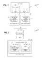
- FIG. 1is a block diagram of a system including a host device 110 that is communicatively coupled to one or more data storage devices, such as “data storage device A” 120 and/or “data storage device B” 125 .
- the host device 110may be coupled to the data storage device(s) over any suitable or desirable communications interface, such as a wired or wireless communication interface.
- the host device 110is coupled to the data storage devices over separate physical interface ports, shown as “port A” 114 and “port B” 115 .
- the ports 114 , 115may be universal serial bus (USB) ports, or the like.
- USBuniversal serial bus
- the data storage devices 120 , 125may each comprise non-volatile storage, illustrated as blocks 140 and 145 , respectively.
- each of the data storage devices 120 , 125is configured to store an operating system.
- data storage device A ( 120 )may store a first operating system 142
- data storage device B ( 125 )may store a second operating system 147 , wherein the first operating system and the second operating system may be different types of operating systems in certain embodiments.
- operating system A ( 142 )may be a Windows, Linux, Mac OS, or other type of Unix-based or other operating system
- operating system B ( 147 )may be a different one of such possible operating systems.
- the non-volatile storage 140 , 145may comprise any type of non-volatile data storage media.
- the non-volatile storagemay comprise magnetic disk media, solid-state media, optical media, or other type of non-volatile storage.
- one or more of the data storage devices 120 , 125may be configured to receive operational power from the host device 110 over a respective port of the host device.
- the host device 110may include one or more power sources 112 , which may be configured to provide power that one or more voltage levels to either or both of the ports 114 , 115 .
- the host device 110may provide bus power for powering rotating disk media associated with the data storage devices 120 , 125 .
- FIG. 2is a block diagram illustrating a system 200 including a host device 210 communicatively coupled to a data storage device 220 .
- the host device 210may be coupled to the data storage device 220 over a communications interface via a communication port 214 of the host device 210 .
- the host device 210is configured to provide power to the data storage device 220 via the port 214 .
- the powermay be provided by a power source 212 of the host device 210 .
- the non-volatile storage 240 of the data storage device 220is partitioned (e.g., using multi-boot utility software/firmware), wherein separate logical containers (“partitions”) are used to house separate filesystems, where operating systems, applications and/or data may be stored.
- each partition of the storageis associated with a separate logical unit number (LUN).
- LUNlogical unit number
- the non-volatile storage 240may be divided into a first partition 241 and a second partition 245 .
- the first partition(e.g., primary partition), or “partition A,” may include a first LUN 244 , identified as “LUN A,” whereas the second partition, or “partition B,” may include a second LUN, identified as “LUN B.”
- LUN A ( 244 )may include a boot record 243 including system data related to booting procedures of the host device 210 and/or data storage device 220 .
- the operating system 242 of the first LUN 244is generally booted up first.
- the host device 210may be configured to boot from the data storage device 220 by loading operating system A ( 242 ) at start-up.
- the host device 210may locate operating system A ( 242 ) on LUN A in the primary partition 241 .
- the host devicemay implement a boot manager program to boot operating system B ( 247 ).
- the partition scheme illustrated in FIG. 2may enable the loading of the second operating system 247 from the second LUN 246 once the first operating system has been booted.
- the host device 210may be configured to execute software that effects the transition from the first operating system 242 to the second operating system 247 .
- the partitions of the non-volatile storage 240may be created by the host 210 using a multi-boot utility program (e.g., “Boot Camp,” by Apple Inc.), which may provide for non-destructive disk partitioning of the non-volatile storage 240 .
- a multi-boot utility programe.g., “Boot Camp,” by Apple Inc.
- disk partitioningmay result in a media in which one partition is substantially susceptible to corruption from corruption of another partition of the media. Such corruption may result in loss of mapping and/or other system data, thereby rendering the filesystem(s) of the non-volatile storage 240 effectively unusable.
- Certain embodiments disclosed hereinallow for the utilization by a host device/system of at least two physically and/or logically separate storage devices/drives for data storage. Connectability of two or more data storage devices/drives may be desirable in a number of situations, such as where the ability to boot from two separate operating systems is desirable. Furthermore, because the connection of physically separate drives can lead to power concerns, as described above, certain embodiments herein advantageously provide two or more separate data storage device/drive connectability in a single physical device/drive, where the host sees two or more separate disks through connection with a single device/drive that requires only enough power for a single drive.
- the host device/system firmwaremay identify each of the physical disks independently. For example, the host may view the separate LUNs as physically different storage devices/drives according to, for example, a JBOD storage management scheme.
- FIG. 3is a block diagram illustrating a system 300 comprising a host device 310 communicatively coupled to a data storage device 320 via a port 314 of the host device 310 .
- the host device 310may be configured to boot from the data storage device 320 .
- the data storage device 320may comprise a single non-volatile storage module 340 (e.g., disk media)
- the host device firmwaremay view the non-volatile storage as two or more separate LUNs ( 344 , 346 ), such as in a JBOD configuration/relationship. With separate JBOD LUNs, the non-volatile storage 340 may provide improved storage features over a partitioned storage, as described above.
- accessmay be provided to a host to only one of the LUNs, or access may be limited to one or more LUNs. Because each LUN ( 344 , 346 ) is viewed as a separate physical disk by the host, corruption of the filesystem of one LUN may not substantially affect the other LUN(s).
- the data storage deviceincludes a controller 330 , which may comprise one or more processors and/or memory modules for directing operation of the data storage device 320 .
- the controller 330may be configured to receive data commands from the host 310 and execute such commands in the non-volatile storage 340 . Such commands may include data read/write commands, and the like.
- the controller 330may be configured to receive data commands from a storage interface (e.g., a device driver) residing on the host 310 .
- Data commandsmay specify a logical block address (LBA) in the data storage device 120 ; data may be accessed/transferred based on such commands.
- LBAlogical block address
- the data access commandsmay also specify a particular LUN among a plurality of LUNs.
- the non-volatile storage 340may comprise magnetic disk storage, for example.
- the non-volatile storage 340may be used to store the plurality of LUN's.
- the plurality of LUNsmay be stored in interleaved manner with respect to logical addressing of the non-volatile storage 340 .
- the data storage device 320can store data received from the host 310 such that the data storage device 320 acts as data storage for the host 310 .
- the controller 330may implement a logical interface for presenting to the host 310 each of the LUNs of the non-volatile storage 340 as a set of logical addresses (e.g., sequential/contiguous addresses) where data can be stored. Internally, the controller 330 can map LUN-specific logical addresses to translated comprehensive LBAs, and further map the translated LBAs to various physical memory addresses in the non-volatile storage 340 .
- mapping dataindicating the mapping of LUN-specific logical addresses to translated comprehensive LBAs, and from translated comprehensive LBAs to physical memory addresses, may be maintained in the data storage device 320 .
- mapping table datamay be stored in non-volatile storage 340 in order to allow for recreation of mapping tables following a power cycle.
- Certain embodiments disclosed hereinprovide for JBOD management of a plurality of LUNs using a single data storage device, wherein non-volatile media of the data storage device is logically and/or physically divided to achieve the same.
- the data storage mediamay be divided in such a way as to substantially equally distributed the LUNs in the inner-diameter and outer-diameter. Such a distribution mechanism may allow substantially equal performance on the plurality of disk LUNs.
- the controller 330may include one or more memory modules (not shown), such as non-volatile memory (e.g., ROM) and/or volatile memory (e.g., RAM, such as DRAM).
- the controller 330may be configured to store information, including, for example, operating system(s) code, application code, system tables and/or other data, in the non-volatile solid-state storage 340 .
- the controller 330may be configured to load such data for use in operation of the data storage device.
- the controller 330 illustrated in FIG. 3may represent a device controller associated with the data storage device 320 and/or a bridge device, wherein address mapping and/or other functionality disclosed herein may be implemented at least in part by the controller/bridge 330 , such as through execution of firmware associated therewith.
- bridge circuitrymay sit between the device controller and the host device 310 , such that the bridge circuitry presents to the device controller the translated comprehensive LBA(s) associated with the host command.
- the controller 330comprises a USB bridge module or device configured to implement certain features disclosed herein.
- the controller/bridge 330may receive data storage commands from the host 310 that include a logical address (LBA) associated with one of the LUNs of the non-volatile storage; that is, the LBA may identify an LUN as well as an LBA of the identified LUN.
- the controller/bridge 330may be configured to take the LUN-specific LBA and translate it to a translated LBA associated with a comprehensive, contiguous range of LBAs of the non-volatile storage that may include all of the LUNs of the non-volatile storage 340 .
- Controller circuitry of the data storage device 320may further map the translated LBA to a physical address associated with the storage media for storage therein.
- the non-volatile storage 340comprises a comprehensive range of LBAs that is sub-divided among the separate LUNs of the storage according to some address division scheme; that is, some or each of the comprehensive LBAs may be associated with a LUN-specific LBA associated with one of the LUNs.
- subsets of contiguous addresses of the comprehensive LBAsare each associated with one of the LUNs. For example, alternating subsets may be associated with the respective LUNs (see, e.g., FIG. 4 ).
- control circuitry 330may be configured to generate a plurality of data storage access commands, one for each of the subsets of LBAs associated with the translated host data addresses.
- the data storage device 320may comprise a single direct-attached storage device (DAS) that is viewed by the host device 310 as a plurality of drives.
- each of the LUNs of the non-volatile storage 340may store a separate operating system ( 342 , 347 ).
- a first LUN 344may include a first operating system 342 and a second LUN 346 may include a second operating system 347 .
- the hostmanages the separate LUNs according to a JBOD scheme. Therefore, operating system A ( 342 ) and operating system B ( 347 ) may not operate on the same partition table.
- each of the LUNsmay be separately partitionable.
- each LUNmay have its own independent boot record, as shown.
- the host device 310 and/or control circuitry 330may be configured to implement firmware that maps a first portion (e.g., approximately half) of the LBAs of the non-volatile storage to LUN A ( 344 ), and a second portion to LUN B ( 346 ).
- firmwaremaps a first portion (e.g., approximately half) of the LBAs of the non-volatile storage to LUN A ( 344 ), and a second portion to LUN B ( 346 ).
- the non-volatile storagecomprises a disk storage module
- chunks of LBAs assigned to respective LUNsare approximately 1 Mb in size. However, chunks of any size or comprising any number of LBAs may be implemented in accordance with embodiments disclosed herein.
- the host device 310may boot from the data storage device 320 at least in part by loading either of the operating systems 342 , 347 . That is, in certain embodiments, it may not be necessary for the host device 310 to initially load a primary operating system prior to loading a secondary operating system. Because each of the operating systems 342 , 347 may be loaded independently of one another, each of the LUN's 344 , 346 may include a separate boot record ( 343 , 348 ). During start-up, the host device system 310 may see two separate LUNs, as well as two separate boot records. Therefore, the host 310 may boot either of the operating systems independently of the other.
- LBAsmay advantageously be divided in such a manner as to promote similar performance between separate LUNs.
- performancemay be at least partially different with respect to physical addresses in a region near an outer diameter of the disk compared to physical addresses in a region near an inner diameter of the disk. Therefore, interleaved, alternating chunks of contiguous LBAs may be implemented to promote evenness of LUN representation across the media.
- such uneven performance concernsmay be less relevant, and therefore certain embodiments may simply assign a first-half portion of the comprehensive LBAs to a first LUN, and a second-half portion to a second LUN.
- FIG. 4is a block diagram illustrating a comprehensive range of logical addresses of non-volatile storage in accordance with one or more embodiments.
- different subsets, or chunks, of contiguous LBAs of a comprehensive range of contiguous LBAsmay be assigned to different LUNs.
- alternating subsets of M contiguous LBAsmay be assigned to different LUNs.
- the subset(s) associated with a first LUN, LUN Aare represented in the diagram of FIG.
- LBA A XLBA A X
- LUN-specific LBA#LBA sub-numbering scheme
- LBA B XLBA sub-numbering scheme
- the collective LBAsprovide a comprehensive contiguous numbering scheme (“comprehensive LBA#) across both LUN A and LUN B.
- the various subsets/chunks of the respective LUNsmay have any number of LBAs, as desired.
- a first half of the comprehensive LBAs of the storagemay be associated with a first LUN, whereas a second half of the LBAs may be associated with the second LUN.
- alternating chunksare associated with the separate LUNs, respectively.
- the performance associated with servicing data access commandsmay be at least partly affected by the size of chunk used, as leap-frogging of chunks for storing/reading data may be required with increased frequency as chunk size is reduced.
- a large enough chunk sizemay be selected such that the vast majority of data access commands may require access to only a single chunk.
- chunk sizesmay correspond to 64 kB, 512 kB, 1 MB, or other value.
- the LBA division scheme implementedmay determine how mapping from LUN-specific LBAs to comprehensive LBAs may be performed.
- LBALUN-specific LBA
- TLBAtranslated comprehensive LBAs
- Such translated command(s)may be provided to a storage device controller (e.g., SATA controller) associated with a non-volatile storage module.
- SATA controllere.g., SATA controller
- Such translationmay be performed at least in part by a bridge controller.
- generation of translated storage access command(s)may involve determining that the address range associated with a host command crosses a boundary of the alternating subsets of LBAs.
- a LUN-specific LBA A 18is received in association with a host command and associated host data
- the data associated with the commandwhen stored in contiguous LUN-specific addresses, crosses over the chunk boundary that ends at comprehensive LBA # 35 , LUN-specific LBA #A 19
- at least a first translated commandmay be generated to access the chunk 401 associated with comprehensive LBA #A 18 , as well as a second translated command to access the next chunk 402 associated with LUN A.
- the second translated commandmay specify the starting address of the chunk 402 (i.e., comprehensive LBA # 40 , LUN-specific LBA #A 20 ). Additional translated command(s) may further be required when the host data spans across additional LUN-specific chunk boundaries.
- the translated storage access command(s)may be provided to non-volatile storage control circuitry configured to map the translated address(es) to physical address(es) and execute the command(s) in the non-volatile storage.
- Determining whether the storage access command crosses a chunk boundarymay be performed in any desirable or practical manner. For example, certain embodiments involve identifying a position of the translated LBA within the chunk associated with the LUN-specific LBA and determining whether an address range associated with the command indicates overlap of a chunk boundary.
- a modulo operationis implemented on each of the LUN-specific LBA#'s or comprehensive LBA#'s associated with the host command using the number of LBAs per chunk (“M”) as the divisor. The remainder of the modulo operation may indicate whether an LBA is at the beginning or end of a chunk, thereby possibly indicating chunk overlap.
- any address of the range of LBAs(LUN-specific or comprehensive), other than the first LBA of the command, is associated with a modulo remainder equal to zero, it may be determined that chunk overlap occurs, and therefore more than one translated storage access command may be necessary.
- generating a second storage access command when multiple translated commands are necessarymay involve identifying a first overlapping LBA within the address range that crosses the boundary of the first LUN-specific chunk associated with the host command, wherein the second storage access command includes a first LBA of the next LUN-specific chunk, data associated with the first overlapping LBA, and a tail address range that comprises a subset of the address range that overlaps the boundary of the first chunk.
- TLBAstranslated LBAs
- LBAsLUN-specific
- ‘M’represents the number of LBAs in a chunk
- ‘/’is a quotient operator
- ‘%’is a modulo operator
- each of the represented LUNsmay be alternatingly assigned to subsets of the comprehensive addressing scheme.
- FIG. 5is a flow diagram illustrating a process 500 for managing data storage according to one or more embodiments.
- the process 500involves receiving a storage access request including an LBA. For example, such request may be received from a host coupled to a data storage device.
- the process 500involves mapping the LBA to a translated LBA based on a LUN identifier associated with the host command. For example, where the received LBA is associated with a first LUN, the LBA may be translated to a first-LUN-specific LBA.
- the process 500involves mapping the translated LBA to a physical block address (PBA).
- PBAphysical block address
- a block 508the process 500 involves accessing the map to PBA.
- the process 500may allow for a relatively easy and/or reliable mechanism for booting multiple different operating systems substantially independently.
- the process 500may be performed at least partially under the control of control circuitry of a data storage device.
- non-volatile solid-state memorymay refer to solid-state memory such as NAND flash.
- Solid-state memorymay comprise a wide variety of technologies, such as flash integrated circuits, Phase Change Memory (PC-RAM or PRAM), Programmable Metallization Cell RAM (PMC-RAM or PMCm), Ovonic Unified Memory (OUM), Resistance RAM (RRAM), NAND memory, NOR memory, EEPROM, Ferroelectric Memory (FeRAM), MRAM, or other discrete NVM (non-volatile solid-state memory) chips.
- PC-RAM or PRAMPhase Change Memory
- PMC-RAM or PMCmProgrammable Metallization Cell RAM
- OFUMOvonic Unified Memory
- RRAMResistance RAM
- NAND memoryNOR memory
- EEPROMFerroelectric Memory
- FeRAMFerroelectric Memory
- MRAMor other discrete NVM (non-volatile solid-state memory) chips.
- non-volatile solid-state memory arrays or storage devicesmay be physically divided into planes, blocks, pages, and sectors, as is known in the art.
- Other forms of storagee.g., battery backed-up volatile DRAM or SRAM devices, magnetic disk drives, etc. may additionally or alternatively be used.
- All of the processes described abovemay be embodied in, and fully automated via, software code modules executed by one or more general purpose or special purpose computers or processors.
- the code modulesmay be stored on any type of computer-readable medium or other computer storage device or collection of storage devices. Some or all of the methods may alternatively be embodied in specialized computer hardware.
Landscapes
- Engineering & Computer Science (AREA)
- Theoretical Computer Science (AREA)
- Software Systems (AREA)
- Physics & Mathematics (AREA)
- General Engineering & Computer Science (AREA)
- General Physics & Mathematics (AREA)
- Computer Security & Cryptography (AREA)
- Techniques For Improving Reliability Of Storages (AREA)
Abstract
Description
TLBA=((LBA/M)×2M)+(LBA%M);
TLBA=((LBA/M)×2M)+(LBA%M)+M; or
TLBA=((LBA/M)×2M)+(LBA%M)−M;
Claims (20)
TLBA=((LBA/M)×2M)+(LBA%M),
TLBA=((LBA/M)×2M)+(LBA%M)+M,
TLBA=((LBA/M)×2M)+(LBA%M),
TLBA=((LBA/M)×2M)+(LBA%M)+M,
Priority Applications (2)
| Application Number | Priority Date | Filing Date | Title |
|---|---|---|---|
| US14/920,834US10102138B2 (en) | 2015-10-22 | 2015-10-22 | Division of data storage in single-storage device architecture |
| PCT/US2016/057713WO2017070217A1 (en) | 2015-10-22 | 2016-10-19 | Division of data storage in single-storage device architecture |
Applications Claiming Priority (1)
| Application Number | Priority Date | Filing Date | Title |
|---|---|---|---|
| US14/920,834US10102138B2 (en) | 2015-10-22 | 2015-10-22 | Division of data storage in single-storage device architecture |
Publications (2)
| Publication Number | Publication Date |
|---|---|
| US20170116131A1 US20170116131A1 (en) | 2017-04-27 |
| US10102138B2true US10102138B2 (en) | 2018-10-16 |
Family
ID=58557788
Family Applications (1)
| Application Number | Title | Priority Date | Filing Date |
|---|---|---|---|
| US14/920,834Active2036-12-09US10102138B2 (en) | 2015-10-22 | 2015-10-22 | Division of data storage in single-storage device architecture |
Country Status (2)
| Country | Link |
|---|---|
| US (1) | US10102138B2 (en) |
| WO (1) | WO2017070217A1 (en) |
Cited By (2)
| Publication number | Priority date | Publication date | Assignee | Title |
|---|---|---|---|---|
| US20200065258A1 (en)* | 2018-08-22 | 2020-02-27 | Western Digital Technologies, Inc. | Logical and physical address field size reduction by alignment-constrained writing technique |
| US20230297282A1 (en)* | 2022-03-16 | 2023-09-21 | Innogrit Technologies Co., Ltd. | Data writing method and apparatus, and storage medium |
Families Citing this family (6)
| Publication number | Priority date | Publication date | Assignee | Title |
|---|---|---|---|---|
| JP6785205B2 (en) | 2017-09-21 | 2020-11-18 | キオクシア株式会社 | Memory system and control method |
| JP7292291B2 (en)* | 2017-10-26 | 2023-06-16 | ユー・アール・フラッシュ エル・エル・シー | Media storage device with multiple partitions |
| JP2019079464A (en) | 2017-10-27 | 2019-05-23 | 東芝メモリ株式会社 | Memory system and control method |
| JP6982468B2 (en) | 2017-10-27 | 2021-12-17 | キオクシア株式会社 | Memory system and control method |
| US10585795B2 (en)* | 2018-05-31 | 2020-03-10 | Micron Technology, Inc. | Data relocation in memory having two portions of data |
| KR20230040114A (en)* | 2021-09-15 | 2023-03-22 | 에스케이하이닉스 주식회사 | Storage device and operating method thereof |
Citations (39)
| Publication number | Priority date | Publication date | Assignee | Title |
|---|---|---|---|---|
| US6499054B1 (en) | 1999-12-02 | 2002-12-24 | Senvid, Inc. | Control and observation of physical devices, equipment and processes by multiple users over computer networks |
| US20030065925A1 (en)* | 2001-10-03 | 2003-04-03 | Tomoyuki Shindo | Information recording apparatus having function of encrypting information |
| US20050144200A1 (en) | 1999-12-02 | 2005-06-30 | Lambertus Hesselink | Managed peer-to-peer applications, systems and methods for distributed data access and storage |
| US20050144195A1 (en) | 1999-12-02 | 2005-06-30 | Lambertus Hesselink | Managed peer-to-peer applications, systems and methods for distributed data access and storage |
| US20060064568A1 (en) | 2004-09-21 | 2006-03-23 | Pak-Lung Seto | Integrated circuit capable of mapping logical block address data across multiple domains |
| US7111121B2 (en) | 2002-05-29 | 2006-09-19 | Hagiwara Sys-Com Co., Ltd. | USB storage device and program |
| US7120692B2 (en) | 1999-12-02 | 2006-10-10 | Senvid, Inc. | Access and control system for network-enabled devices |
| US20070204128A1 (en) | 2003-09-10 | 2007-08-30 | Super Talent Electronics Inc. | Two-Level RAM Lookup Table for Block and Page Allocation and Wear-Leveling in Limited-Write Flash-Memories |
| US20070282951A1 (en)* | 2006-02-10 | 2007-12-06 | Selimis Nikolas A | Cross-domain solution (CDS) collaborate-access-browse (CAB) and assured file transfer (AFT) |
| US7454443B2 (en) | 2003-08-26 | 2008-11-18 | Tamir Ram | Method, system, and program for personal data management using content-based replication |
| US7546353B2 (en) | 1999-12-02 | 2009-06-09 | Western Digital Technologies, Inc. | Managed peer-to-peer applications, systems and methods for distributed data access and storage |
| US20090222496A1 (en)* | 2005-06-24 | 2009-09-03 | Syncsort Incorporated | System and Method for Virtualizing Backup Images |
| US7587467B2 (en) | 1999-12-02 | 2009-09-08 | Western Digital Technologies, Inc. | Managed peer-to-peer applications, systems and methods for distributed data access and storage |
| US7917628B2 (en) | 1999-12-02 | 2011-03-29 | Western Digital Technologies, Inc. | Managed peer-to-peer applications, systems and methods for distributed data access and storage |
| US7934251B2 (en) | 1999-12-02 | 2011-04-26 | Western Digital Technologies, Inc. | Managed peer-to-peer applications, systems and methods for distributed data access and storage |
| US7949564B1 (en) | 2000-05-31 | 2011-05-24 | Western Digital Technologies, Inc. | System and method of receiving advertisement content from advertisers and distributing the advertising content to a network of personal computers |
| US8004791B2 (en) | 2008-02-22 | 2011-08-23 | Western Digital Technologies, Inc. | Information storage device with a bridge controller and a plurality of electrically coupled conductive shields |
| US20120036041A1 (en) | 2010-08-09 | 2012-02-09 | Western Digital Technologies, Inc. | Methods and systems for a personal multimedia content archive |
| US8255661B2 (en) | 2009-11-13 | 2012-08-28 | Western Digital Technologies, Inc. | Data storage system comprising a mapping bridge for aligning host block size with physical block size of a data storage device |
| US8285965B2 (en) | 2009-11-20 | 2012-10-09 | Western Digital Technologies, Inc. | Aligning data storage device partition to boundary of physical data sector |
| US8352567B2 (en) | 1999-12-02 | 2013-01-08 | Western Digital Technologies, Inc. | VCR webification |
| US20130179626A1 (en) | 2012-01-06 | 2013-07-11 | Phison Electronics Corp. | Data processing method, memory controller and memory storage apparatus |
| US20130212401A1 (en) | 2012-02-14 | 2013-08-15 | Western Digital Technologies, Inc. | Methods and devices for authentication and data encryption |
| US8526798B2 (en) | 2009-12-23 | 2013-09-03 | Western Digital Technologies, Inc. | Portable content container displaying A/V files in response to a command received from a consumer device |
| US20130268771A1 (en) | 2012-04-10 | 2013-10-10 | Western Digital Technologies, Inc. | Digital rights management system and methods for accessingcontent from an intelligent storag |
| US20130268759A1 (en) | 2012-04-10 | 2013-10-10 | Western Digital Technologies, Inc. | Digital rights management system transfer of content and distribution |
| US8631284B2 (en) | 2010-04-30 | 2014-01-14 | Western Digital Technologies, Inc. | Method for providing asynchronous event notification in systems |
| US8646054B1 (en) | 2012-03-23 | 2014-02-04 | Western Digital Technologies, Inc. | Mechanism to manage access to user data area with bridged direct-attached storage devices |
| US20140084850A1 (en)* | 2012-09-24 | 2014-03-27 | Samsung Electronics Co., Ltd. | Host apparatus, user terminal apparatus, method of controlling charger, and method of communication using the same |
| US8688797B2 (en) | 1999-12-02 | 2014-04-01 | Western Digital Technologies, Inc. | Managed peer-to-peer applications, systems and methods for distributed data access and storage |
| US20140095439A1 (en) | 2012-10-01 | 2014-04-03 | Western Digital Technologies, Inc. | Optimizing data block size for deduplication |
| US8713265B1 (en) | 2010-09-21 | 2014-04-29 | Western Digital Technologies, Inc. | Visual indicator of online backup |
| US20140169921A1 (en) | 2012-12-19 | 2014-06-19 | Mark Carey | Cargo carrier |
| US20140173215A1 (en) | 2012-12-13 | 2014-06-19 | Western Digital Technologies, Inc. | Methods and systems for provisioning a bootable image on to an external drive |
| US8762682B1 (en) | 2010-07-02 | 2014-06-24 | Western Digital Technologies, Inc. | Data storage apparatus providing host full duplex operations using half duplex storage devices |
| US8780004B1 (en) | 2012-01-31 | 2014-07-15 | Western Digital Technologies, Inc. | Dual configuration enclosure with optional shielding |
| US8838892B2 (en) | 2012-12-28 | 2014-09-16 | Huawei Technologies Co., Ltd. | Data storage method and storage device |
| US20140281312A1 (en) | 2013-03-15 | 2014-09-18 | Skyera, Inc. | Apparatus and method for translation from multi-dimensional tolinear address space in storage |
| US9547459B1 (en)* | 2013-06-27 | 2017-01-17 | EMC IP Holding Company LLC | Techniques for data relocation based on access patterns |
Family Cites Families (1)
| Publication number | Priority date | Publication date | Assignee | Title |
|---|---|---|---|---|
| US7743214B2 (en)* | 2005-08-16 | 2010-06-22 | Mark Adams | Generating storage system commands |
- 2015
- 2015-10-22USUS14/920,834patent/US10102138B2/enactiveActive
- 2016
- 2016-10-19WOPCT/US2016/057713patent/WO2017070217A1/ennot_activeCeased
Patent Citations (50)
| Publication number | Priority date | Publication date | Assignee | Title |
|---|---|---|---|---|
| US8352567B2 (en) | 1999-12-02 | 2013-01-08 | Western Digital Technologies, Inc. | VCR webification |
| US6499054B1 (en) | 1999-12-02 | 2002-12-24 | Senvid, Inc. | Control and observation of physical devices, equipment and processes by multiple users over computer networks |
| US6732158B1 (en) | 1999-12-02 | 2004-05-04 | Senvid, Inc. | VCR webification |
| US20050144200A1 (en) | 1999-12-02 | 2005-06-30 | Lambertus Hesselink | Managed peer-to-peer applications, systems and methods for distributed data access and storage |
| US20050144195A1 (en) | 1999-12-02 | 2005-06-30 | Lambertus Hesselink | Managed peer-to-peer applications, systems and methods for distributed data access and storage |
| US8793374B2 (en) | 1999-12-02 | 2014-07-29 | Western Digital Technologies, Inc. | Managed peer-to-peer applications, systems and methods for distributed data access and storage |
| US7934251B2 (en) | 1999-12-02 | 2011-04-26 | Western Digital Technologies, Inc. | Managed peer-to-peer applications, systems and methods for distributed data access and storage |
| US7120692B2 (en) | 1999-12-02 | 2006-10-10 | Senvid, Inc. | Access and control system for network-enabled devices |
| US8661507B1 (en) | 1999-12-02 | 2014-02-25 | Western Digital Technologies, Inc. | Managed peer-to-peer applications, systems and methods for distributed data access and storage |
| US7917628B2 (en) | 1999-12-02 | 2011-03-29 | Western Digital Technologies, Inc. | Managed peer-to-peer applications, systems and methods for distributed data access and storage |
| US7546353B2 (en) | 1999-12-02 | 2009-06-09 | Western Digital Technologies, Inc. | Managed peer-to-peer applications, systems and methods for distributed data access and storage |
| US7467187B2 (en) | 1999-12-02 | 2008-12-16 | Western Digital Technologies, Inc. | Control and observation of physical devices, equipment and processes by multiple users over computer networks |
| US8341275B1 (en) | 1999-12-02 | 2012-12-25 | Western Digital Technologies, Inc. | Access and control system for network-enabled devices |
| US8688797B2 (en) | 1999-12-02 | 2014-04-01 | Western Digital Technologies, Inc. | Managed peer-to-peer applications, systems and methods for distributed data access and storage |
| US7587467B2 (en) | 1999-12-02 | 2009-09-08 | Western Digital Technologies, Inc. | Managed peer-to-peer applications, systems and methods for distributed data access and storage |
| US7600036B2 (en) | 1999-12-02 | 2009-10-06 | Western Digital Technologies, Inc. | Access and control system for network-enabled devices |
| US7788404B2 (en) | 1999-12-02 | 2010-08-31 | Western Digital Technologies, Inc. | Access and control system for network-enabled devices |
| US7949564B1 (en) | 2000-05-31 | 2011-05-24 | Western Digital Technologies, Inc. | System and method of receiving advertisement content from advertisers and distributing the advertising content to a network of personal computers |
| US20030065925A1 (en)* | 2001-10-03 | 2003-04-03 | Tomoyuki Shindo | Information recording apparatus having function of encrypting information |
| US7111121B2 (en) | 2002-05-29 | 2006-09-19 | Hagiwara Sys-Com Co., Ltd. | USB storage device and program |
| US8341117B2 (en) | 2003-08-26 | 2012-12-25 | Arkeia Software, Inc. | Method, system, and program for personal data management using content-based replication |
| US7454443B2 (en) | 2003-08-26 | 2008-11-18 | Tamir Ram | Method, system, and program for personal data management using content-based replication |
| US20070204128A1 (en) | 2003-09-10 | 2007-08-30 | Super Talent Electronics Inc. | Two-Level RAM Lookup Table for Block and Page Allocation and Wear-Leveling in Limited-Write Flash-Memories |
| US20060064568A1 (en) | 2004-09-21 | 2006-03-23 | Pak-Lung Seto | Integrated circuit capable of mapping logical block address data across multiple domains |
| US20090222496A1 (en)* | 2005-06-24 | 2009-09-03 | Syncsort Incorporated | System and Method for Virtualizing Backup Images |
| US20070282951A1 (en)* | 2006-02-10 | 2007-12-06 | Selimis Nikolas A | Cross-domain solution (CDS) collaborate-access-browse (CAB) and assured file transfer (AFT) |
| US8004791B2 (en) | 2008-02-22 | 2011-08-23 | Western Digital Technologies, Inc. | Information storage device with a bridge controller and a plurality of electrically coupled conductive shields |
| US8255661B2 (en) | 2009-11-13 | 2012-08-28 | Western Digital Technologies, Inc. | Data storage system comprising a mapping bridge for aligning host block size with physical block size of a data storage device |
| US8285965B2 (en) | 2009-11-20 | 2012-10-09 | Western Digital Technologies, Inc. | Aligning data storage device partition to boundary of physical data sector |
| US8526798B2 (en) | 2009-12-23 | 2013-09-03 | Western Digital Technologies, Inc. | Portable content container displaying A/V files in response to a command received from a consumer device |
| US8631284B2 (en) | 2010-04-30 | 2014-01-14 | Western Digital Technologies, Inc. | Method for providing asynchronous event notification in systems |
| US8762682B1 (en) | 2010-07-02 | 2014-06-24 | Western Digital Technologies, Inc. | Data storage apparatus providing host full duplex operations using half duplex storage devices |
| US20120036041A1 (en) | 2010-08-09 | 2012-02-09 | Western Digital Technologies, Inc. | Methods and systems for a personal multimedia content archive |
| US8713265B1 (en) | 2010-09-21 | 2014-04-29 | Western Digital Technologies, Inc. | Visual indicator of online backup |
| US20130179626A1 (en) | 2012-01-06 | 2013-07-11 | Phison Electronics Corp. | Data processing method, memory controller and memory storage apparatus |
| US8780004B1 (en) | 2012-01-31 | 2014-07-15 | Western Digital Technologies, Inc. | Dual configuration enclosure with optional shielding |
| US8819443B2 (en) | 2012-02-14 | 2014-08-26 | Western Digital Technologies, Inc. | Methods and devices for authentication and data encryption |
| US20130212401A1 (en) | 2012-02-14 | 2013-08-15 | Western Digital Technologies, Inc. | Methods and devices for authentication and data encryption |
| US8646054B1 (en) | 2012-03-23 | 2014-02-04 | Western Digital Technologies, Inc. | Mechanism to manage access to user data area with bridged direct-attached storage devices |
| US20130266137A1 (en) | 2012-04-10 | 2013-10-10 | Western Digital Technologies, Inc. | Digital rights managment system, devices, and methods for binding content to an intelligent storage device |
| US20130268759A1 (en) | 2012-04-10 | 2013-10-10 | Western Digital Technologies, Inc. | Digital rights management system transfer of content and distribution |
| US20130268749A1 (en) | 2012-04-10 | 2013-10-10 | Western Digital Technologies, Inc. | Digital rights management system and methods for provisioning content to an intelligent storage |
| US20130268771A1 (en) | 2012-04-10 | 2013-10-10 | Western Digital Technologies, Inc. | Digital rights management system and methods for accessingcontent from an intelligent storag |
| US20140084850A1 (en)* | 2012-09-24 | 2014-03-27 | Samsung Electronics Co., Ltd. | Host apparatus, user terminal apparatus, method of controlling charger, and method of communication using the same |
| US20140095439A1 (en) | 2012-10-01 | 2014-04-03 | Western Digital Technologies, Inc. | Optimizing data block size for deduplication |
| US20140173215A1 (en) | 2012-12-13 | 2014-06-19 | Western Digital Technologies, Inc. | Methods and systems for provisioning a bootable image on to an external drive |
| US20140169921A1 (en) | 2012-12-19 | 2014-06-19 | Mark Carey | Cargo carrier |
| US8838892B2 (en) | 2012-12-28 | 2014-09-16 | Huawei Technologies Co., Ltd. | Data storage method and storage device |
| US20140281312A1 (en) | 2013-03-15 | 2014-09-18 | Skyera, Inc. | Apparatus and method for translation from multi-dimensional tolinear address space in storage |
| US9547459B1 (en)* | 2013-06-27 | 2017-01-17 | EMC IP Holding Company LLC | Techniques for data relocation based on access patterns |
Non-Patent Citations (1)
| Title |
|---|
| International Search Report and Written Opinion for PCT/US2016/057713 dated Feb. 2, 2017. |
Cited By (5)
| Publication number | Priority date | Publication date | Assignee | Title |
|---|---|---|---|---|
| US20200065258A1 (en)* | 2018-08-22 | 2020-02-27 | Western Digital Technologies, Inc. | Logical and physical address field size reduction by alignment-constrained writing technique |
| US10725931B2 (en)* | 2018-08-22 | 2020-07-28 | Western Digital Technologies, Inc. | Logical and physical address field size reduction by alignment-constrained writing technique |
| US11288204B2 (en) | 2018-08-22 | 2022-03-29 | Western Digital Technologies, Inc. | Logical and physical address field size reduction by alignment-constrained writing technique |
| US20230297282A1 (en)* | 2022-03-16 | 2023-09-21 | Innogrit Technologies Co., Ltd. | Data writing method and apparatus, and storage medium |
| US12159060B2 (en)* | 2022-03-16 | 2024-12-03 | Innogrit Technologies Co., Ltd. | Data writing method and apparatus, and storage medium |
Also Published As
| Publication number | Publication date |
|---|---|
| US20170116131A1 (en) | 2017-04-27 |
| WO2017070217A1 (en) | 2017-04-27 |
Similar Documents
| Publication | Publication Date | Title |
|---|---|---|
| US10102138B2 (en) | Division of data storage in single-storage device architecture | |
| US12216931B1 (en) | Techniques for directed data migration | |
| US8054686B2 (en) | Flash memory storage apparatus, flash memory controller, and switching method thereof | |
| US8930671B2 (en) | Logical address offset in response to detecting a memory formatting operation | |
| US8312554B2 (en) | Method of hiding file at data protecting mode for non-volatile memory module, memory controller and portable memory storage apparatus | |
| CN107908571B (en) | Data writing method, flash memory device and storage equipment | |
| US10089023B2 (en) | Data management for object based storage | |
| US20180004559A1 (en) | Controlling access to namespaces of a storage device | |
| CN107632939A (en) | Mapping table for storage device | |
| US8914608B2 (en) | Data storage device and computing system including the same | |
| WO2017066601A1 (en) | Method and apparatus for providing hybrid mode to access ssd drive | |
| US11010079B2 (en) | Concept for storing file system metadata within solid-stage storage devices | |
| KR102585883B1 (en) | Operating method of memory system and memory system | |
| KR20130064521A (en) | Data storage device and data management method thereof | |
| TWI479505B (en) | Data management method, memory controller and memory storage apparatus | |
| US20170010810A1 (en) | Method and Apparatus for Providing Wear Leveling to Non-Volatile Memory with Limited Program Cycles Using Flash Translation Layer | |
| US20130275655A1 (en) | Memory management method and memory controller and memory storage device using the same | |
| US20150234595A1 (en) | Storage device | |
| US10126987B2 (en) | Storage devices and methods for controlling a storage device | |
| US8954692B2 (en) | File protecting method and system, and memory controller and memory storage apparatus thereof | |
| US9158678B2 (en) | Memory address management system and method | |
| US12079635B2 (en) | Data storage device and method for storage-class-memory-accelerated boot partition optimization | |
| TWI741296B (en) | Method and apparatuse and computer program product for handling sudden power off recovery | |
| US20170277474A1 (en) | Data processing system including data storage device | |
| TW202147126A (en) | Method and apparatuse and computer program product for handling sudden power off recovery |
Legal Events
| Date | Code | Title | Description |
|---|---|---|---|
| AS | Assignment | Owner name:WESTERN DIGITAL TECHNOLOGIES, INC., CALIFORNIA Free format text:ASSIGNMENT OF ASSIGNORS INTEREST;ASSIGNOR:LIN, TINO;REEL/FRAME:036936/0159 Effective date:20151030 | |
| AS | Assignment | Owner name:JPMORGAN CHASE BANK, N.A., AS COLLATERAL AGENT, IL Free format text:SECURITY AGREEMENT;ASSIGNOR:WESTERN DIGITAL TECHNOLOGIES, INC.;REEL/FRAME:038722/0229 Effective date:20160512 Owner name:JPMORGAN CHASE BANK, N.A., AS COLLATERAL AGENT, IL Free format text:SECURITY AGREEMENT;ASSIGNOR:WESTERN DIGITAL TECHNOLOGIES, INC.;REEL/FRAME:038744/0481 Effective date:20160512 Owner name:U.S. BANK NATIONAL ASSOCIATION, AS COLLATERAL AGEN Free format text:SECURITY AGREEMENT;ASSIGNOR:WESTERN DIGITAL TECHNOLOGIES, INC.;REEL/FRAME:038744/0281 Effective date:20160512 Owner name:JPMORGAN CHASE BANK, N.A., AS COLLATERAL AGENT, ILLINOIS Free format text:SECURITY AGREEMENT;ASSIGNOR:WESTERN DIGITAL TECHNOLOGIES, INC.;REEL/FRAME:038722/0229 Effective date:20160512 Owner name:JPMORGAN CHASE BANK, N.A., AS COLLATERAL AGENT, ILLINOIS Free format text:SECURITY AGREEMENT;ASSIGNOR:WESTERN DIGITAL TECHNOLOGIES, INC.;REEL/FRAME:038744/0481 Effective date:20160512 Owner name:U.S. BANK NATIONAL ASSOCIATION, AS COLLATERAL AGENT, CALIFORNIA Free format text:SECURITY AGREEMENT;ASSIGNOR:WESTERN DIGITAL TECHNOLOGIES, INC.;REEL/FRAME:038744/0281 Effective date:20160512 | |
| AS | Assignment | Owner name:WESTERN DIGITAL TECHNOLOGIES, INC., CALIFORNIA Free format text:RELEASE BY SECURED PARTY;ASSIGNOR:U.S. BANK NATIONAL ASSOCIATION, AS COLLATERAL AGENT;REEL/FRAME:045501/0714 Effective date:20180227 | |
| STCF | Information on status: patent grant | Free format text:PATENTED CASE | |
| AS | Assignment | Owner name:WESTERN DIGITAL TECHNOLOGIES, INC., CALIFORNIA Free format text:RELEASE OF SECURITY INTEREST AT REEL 038744 FRAME 0481;ASSIGNOR:JPMORGAN CHASE BANK, N.A.;REEL/FRAME:058982/0556 Effective date:20220203 | |
| MAFP | Maintenance fee payment | Free format text:PAYMENT OF MAINTENANCE FEE, 4TH YEAR, LARGE ENTITY (ORIGINAL EVENT CODE: M1551); ENTITY STATUS OF PATENT OWNER: LARGE ENTITY Year of fee payment:4 | |
| AS | Assignment | Owner name:JPMORGAN CHASE BANK, N.A., ILLINOIS Free format text:PATENT COLLATERAL AGREEMENT - A&R LOAN AGREEMENT;ASSIGNOR:WESTERN DIGITAL TECHNOLOGIES, INC.;REEL/FRAME:064715/0001 Effective date:20230818 Owner name:JPMORGAN CHASE BANK, N.A., ILLINOIS Free format text:PATENT COLLATERAL AGREEMENT - DDTL LOAN AGREEMENT;ASSIGNOR:WESTERN DIGITAL TECHNOLOGIES, INC.;REEL/FRAME:067045/0156 Effective date:20230818 |