US10101373B2 - Capacitive imaging device with active pixels and method - Google Patents
Capacitive imaging device with active pixels and methodDownload PDFInfo
- Publication number
- US10101373B2 US10101373B2US14/257,566US201414257566AUS10101373B2US 10101373 B2US10101373 B2US 10101373B2US 201414257566 AUS201414257566 AUS 201414257566AUS 10101373 B2US10101373 B2US 10101373B2
- Authority
- US
- United States
- Prior art keywords
- source follower
- capacitive image
- transistor
- follower transistor
- pixel
- Prior art date
- Legal status (The legal status is an assumption and is not a legal conclusion. Google has not performed a legal analysis and makes no representation as to the accuracy of the status listed.)
- Active, expires
Links
Images


Classifications
- G—PHYSICS
- G06—COMPUTING OR CALCULATING; COUNTING
- G06V—IMAGE OR VIDEO RECOGNITION OR UNDERSTANDING
- G06V40/00—Recognition of biometric, human-related or animal-related patterns in image or video data
- G06V40/10—Human or animal bodies, e.g. vehicle occupants or pedestrians; Body parts, e.g. hands
- G06V40/12—Fingerprints or palmprints
- G06V40/13—Sensors therefor
- G06V40/1306—Sensors therefor non-optical, e.g. ultrasonic or capacitive sensing
- G—PHYSICS
- G01—MEASURING; TESTING
- G01R—MEASURING ELECTRIC VARIABLES; MEASURING MAGNETIC VARIABLES
- G01R27/00—Arrangements for measuring resistance, reactance, impedance, or electric characteristics derived therefrom
- G01R27/02—Measuring real or complex resistance, reactance, impedance, or other two-pole characteristics derived therefrom, e.g. time constant
- G01R27/26—Measuring inductance or capacitance; Measuring quality factor, e.g. by using the resonance method; Measuring loss factor; Measuring dielectric constants ; Measuring impedance or related variables
- G01R27/2605—Measuring capacitance
- G—PHYSICS
- G06—COMPUTING OR CALCULATING; COUNTING
- G06F—ELECTRIC DIGITAL DATA PROCESSING
- G06F3/00—Input arrangements for transferring data to be processed into a form capable of being handled by the computer; Output arrangements for transferring data from processing unit to output unit, e.g. interface arrangements
- G06F3/01—Input arrangements or combined input and output arrangements for interaction between user and computer
- G06F3/03—Arrangements for converting the position or the displacement of a member into a coded form
- G06F3/041—Digitisers, e.g. for touch screens or touch pads, characterised by the transducing means
- G06F3/0416—Control or interface arrangements specially adapted for digitisers
- G—PHYSICS
- G06—COMPUTING OR CALCULATING; COUNTING
- G06F—ELECTRIC DIGITAL DATA PROCESSING
- G06F3/00—Input arrangements for transferring data to be processed into a form capable of being handled by the computer; Output arrangements for transferring data from processing unit to output unit, e.g. interface arrangements
- G06F3/01—Input arrangements or combined input and output arrangements for interaction between user and computer
- G06F3/03—Arrangements for converting the position or the displacement of a member into a coded form
- G06F3/041—Digitisers, e.g. for touch screens or touch pads, characterised by the transducing means
- G06F3/044—Digitisers, e.g. for touch screens or touch pads, characterised by the transducing means by capacitive means
- G06K9/0002—
Definitions
- the present disclosurerelates to electronic imaging technology and, more particularly, to a capacitive image sensor utilizing capacitive image pixels that have a two-transistor configuration.
- Imaging modalitiesThere are many imaging modalities routinely used today for various types of filmless x-rays and fingerprint sensing. Examples include optical imaging, which is the predominant imaging technique for fingerprints, ultrasonic imaging, and capacitive imaging. For each of the specific imaging techniques there are pros and cons.
- Optical imagingproduces a pattern of light and dark that makes up a visual impression of a fingerprint with components that are easily obtained and inexpensive.
- that visual image produced under optical imagingcan be tainted by stray light or surface contamination of the imaging plate.
- Ultrasonic imagingenables the user to see beneath the skin providing more information as a biometric measure.
- ultrasonic imagingis slow, expensive, bulky, and data intensive.
- Capacitive imagingis widely used for small size finger print sensors, e.g., line scanners or single finger areas, because of its simple structure.
- large area finger print scannersi.e., those having a so-called 4-4-1 format
- capacitive imaging techniqueshas proven difficult due to unreasonable component costs and difficulties in meeting an optimal signal-to-noise ratio.
- a capacitive image sensor of an example embodimentincludes a sensor array having capacitive image pixels. Each pixel has a two-transistor configuration including a pixel selection transistor and a source follower transistor. The pixel selection transistor activates the source follower transistor. The source follower is coupled to a variable capacitance that affects an input impedance of the source follower. An AC current source is used to interrogate the activated source follower to determine an output impedance of the source follower. The output impedance is a function of the input impedance and is representative of the nearness of an object. The combination of all output impedances from all pixels is used to create an image of the object.
- the variable capacitancevaries in accordance with the nearness of the object which is affective in altering capacitance.
- the sensor and/or pixelmay further include a DC current source that is used to set a working bias point for the pixel circuit.
- the AC current sourceprovides a known amplitude and frequency, and may provide a sinusoidal signal or a square-wave signal.
- the sensor and/or pixelmay be implemented with thin film technology. The sensor may provide a resolution of up to about 1000 ppi (pixels per inch).
- a method to obtain an impedance readout from the capacitive image pixelincludes activating the source follower transistor with the pixel selection transistor, interrogating the source follower transistor by applying an AC current source to the source follower transistor, and determining an output impedance of the source follower transistor based on the interrogation.
- the output impedanceis a function of the input impedance and, as such, is representative of the nearness of an object that is capable of affecting the variable capacitance.
- the methodmay additionally include measuring the voltage output of the source follower transistor wherein the voltage output correlates to the output impedance.
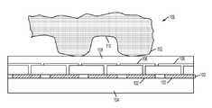
- FIG. 1is a cross-sectional view of a capacitive touch pattern sensor according to an example embodiment.
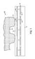
- FIG. 2is a block diagram illustrating details of a sensor array according to an example embodiment.
- FIG. 3is a schematic diagram illustrating an active pixel circuit disclosed in an earlier-filed disclosure (PRIOR ART).
- FIG. 4is a schematic diagram illustrating an active pixel circuit according to an example embodiment.
- FIG. 5is a schematic of a source follower circuit, a standard equivalent of the source follower circuit and the derived output impedance of the source follower circuit.
- FIG. 6is a graph illustrating results of a SPICE simulation of a pixel configured as shown in FIG. 4 .
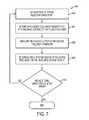
- FIG. 7is a flowchart illustrating a procedure according to an example embodiment.
- the present disclosurerelates to touch/proximity pattern sensors such as fingerprint sensors.
- fingerprintsand similar patterns, e.g., on hands and feet
- computer scanned hand/fingerprint imagescan be used for purposes such as authentication.
- a scanning sensormay include a flat surface against which to place the finger (or any scanned object).
- the sensorIn response to the contact, the sensor generates an image of the texture/contours of the scanned object.
- Pattern recognition softwarecan compare metrics of the scanned image to stored metrics, and confirm identity based on a match of the metrics.
- a fingerprint imagecan be obtained, such as using optical sensors.
- Embodiments described belowuse capacitive sensing.
- an object that touches a sensing surfacewill affect the local electrical capacitance of the surface wherever there is contact.
- capacitive touch input sensingis widely used to determine coarse indications of contact location (e.g., touchscreens, touchpads)
- the sensors described hereinmay be capable of much higher resolution (e.g., on the order of 1000 dpi) than a conventional touch input sensor.
- devicessuch as non-destructive testing imagers may obtain an image based on portions of an object that touch and/or are in relatively close proximity to a contact sensing element.
- FIG. 1a cross-sectional view illustrates a capacitive touch pattern sensor according to an example embodiment.
- a sensor array 102is built on top of a substrate 104 (e.g., glass).
- the sensor array 102includes a plurality of active pixels 100 , an example of which will be described further below.
- each pixel 100is electrically coupled to sensing pads 106 .
- the pads 106are electrically conductive and covered by an insulator layer 108 .
- the insulator layer 108may be made from a protecting coating polymer such as Parylene.
- a conductive object 109 contacting the insulating layer 108changes a local capacitance at the pads 106 .
- a fingerprint ridge 112that is different than another pad 106 directly below fingerprint valley 110 .
- the capacitancemay vary not only based on contact versus non-contact, but may also vary depending on the relative proximity of non-contacting portions. For example, different fingerprint valleys may cause different capacitance due to different distances from a surface of the insulating layer 108 .
- FIG. 2a block diagram illustrates details of a sensor array 102 according to an example embodiment.
- the sensor array 102includes a number of individual active pixel elements 100 . Each of these elements 100 are associated with one of a row line 204 and a column line 206 .
- each of the row lines 204may be activated in sequence. Activating a row line 204 causes all elements 100 in the rows to become active (e.g., switching on an enabling transistor).
- each of the column lines (e.g., data lines) 206is scanned to read the individual elements 100 in the currently activated row. Alternate methods of scanning the elements 100 are known in the art, and the embodiments need not be limited to what is shown in FIG. 2 .
- each column line 206may involve applying to each column line 206 a first voltage level for a first period of time, then switching to a second, lower voltage level for a second period of time.
- the first voltage levelcharges the currently read element 100 and the second voltage level causes a current flow via the column line that indicates a sensed capacitance of the element 100 .
- FIG. 3a schematic diagram illustrates an active pixel 100 according to a previously disclosed, prior art embodiment which may be found in U.S. Pat. No. 8,618,865.
- the active pixel 100is generally configured as a three-transistor sensor, sometimes abbreviated as a 3 T sensor pixel.
- the three transistors M 1 , M 2 , M 3 in this diagramare n-type, low-temperature, polycrystalline silicon (Poly-si) thin film transistors (TFTs) although it may be possible to use other types of transistor devices such as metal oxide semiconductor, field-effect transistors (MOSFETs).
- Transistor M 2is configured as a reset transistor in response to reset signal G n+1 .
- M 2When G n+1 is activated, M 2 shorts out high frequency rectifying/detection diode D 1 , allowing sensing junction J 1 to be tied to the biasing voltage of D 1 .
- the reset transistor M 2By tying the reset transistor M 2 to the enable line of the following row (G n+1 ), the active pixels 100 can be reset without using a separate set of reset lines. In other configurations, M 2 may be reset by another line, such as the preceding row enable (G n+1 ), a separate reset line, a data line Dn of an adjacent column, etc.
- the C p componentis a parasitic capacitor, having one end coupled to the sensing junction J 1 and the other end at ground.
- the C f componentmodels the sensed capacitance of the pads and insulating layer (see sensing pads 106 and insulating layer 108 in FIG. 1 ).
- the effective value of C fmay vary from zero (or near zero) to some maximum value (in this example on the order of 10 fF) depending on whether or not an object (e.g., fingerprint ridge) is contacting the insulating layer.
- the sensed capacitancecan be found based on a ratio of gate capacitance of M 1 (C M1 ) and the sum of C f , C p , and C M1 .
- the M 1 transistoris configured as a source follower having its gate tied to the sensing junction J 1 .
- the output of M 1is tied to data line Dn when enabling transistor M 3 is switched on in response to enable signal Gn.
- the transistor M 1also acts as a charge pump to charge up capacitors C f and C p . This charging occurs during the operation cycle of the pixel 100 , when M 3 is enabled. In one prior art embodiment, the operation cycle is between 50-50 ⁇ s.
- the charge accumulated on the gate of M 1 during charging intervalwill be redistributed among C p , C f , and C M1 .
- the final voltage (V sense ) at the sensing junction J 1 at the end of the sensing intervalbecomes the input of the source follower M 1 , and the output of M 1 at this interval can be read out on Dn.
- the difference ⁇ V between the V charge and V sense potentialscan be expressed as ⁇ V is approximately proportional to C M1 /(C f +C p +C M1 ).
- the capacitance C fmay be determined by measuring current flow through Dn during the sensing interval.
- the active pixel 100provides a good signal-to-noise ratio
- three transistors and a diodeare required to form the active pixel 100 .
- the resultis a scanner that could provide a pixel density of approximately 500 ppi.
- technology requirementsare ever-expanding and there is a desire to produce an active pixel with up to double the pixel density, i.e. 1000 ppi.
- a 1000 ppi pixel densityis difficult to achieve using the above-described prior art design without using design rules that would exceed most TFT manufacturer's capabilities.
- a pixel design for an active pixelwherein only two transistors are required yet a desired 1000 ppi pixel density is substantially achieved and manufacturability is eased.
- an active pixel 300 of an example embodimentis disclosed.
- the design of active pixel 300has been streamlined from that of FIG. 3 to eliminate the diode D 1 and the reset transistor M 2 .
- the remaining transistorscomprise a source follower transistor M 1 and a pixel selection transistor M 3 .
- a series capacitancecomprising C 3 and C f is connected to junction J 1 as is capacitor C p .
- C prepresents the parasitic capacitance of the pixel 300 while C f models the sensed capacitance of the pads and insulating layer (see sensing pads 106 and insulating layer 108 in FIG. 1 ).
- the series capacitance of C f and C 3which itself has a value of C x , has a combined capacitive value that may vary from zero (or near zero) to some maximum value, e.g., on the order of about 13.3 fF, depending on whether or not an object (e.g., fingerprint ridge) is contacting or near the insulating layer 108 .
- the value of C xis essentially the object to imager platen, i.e., substrate 104 , capacitance.
- the M 1 transistor of FIG. 4is configured as a source follower having its gate tied to the sensing junction J 1 .
- Resistor R 1provides this path.
- Resistor R 1may comprise a semi-insulative layer covering all of the pixels 300 and is tied to supply voltage V cc . In a simulation of the pixel 300 a value of 1e13 Ohms was used for R 1 , however, R 1 may be any value as long as the value is much greater than the impedance of C p at a probing frequency, described further below, of the readout process.
- I 1 and I 2are DC and AC current sources, respectively, that either are implemented at the peripheral of substrate 104 using TFT technology or provided by a readout chip.
- I 1is the DC source operating to ensure that a correct working bias point is set.
- I 2is the “probing” AC source operating to provide a known amplitude and frequency current to the pixel 300 .
- the output impedance of the source follower M 1is interrogated by injecting the AC current I 2 and measuring the voltage response which thereby enables a determination of the output impedance of M 1 as a function of its input impedance.
- the input impedancevaries in accordance with the distance of an object from the insulating layer 108 .
- a standard source follower circuit, equivalent circuit, and the derived output impedance as a function of input impedanceare shown in FIG. 5 .
- a plurality of pixels 300are substituted for pixels 100 and incorporated into an array 102 of pixels such as that shown in FIG. 2 .
- an array 102 of pixelssuch as that shown in FIG. 2 .
- a flowchartillustrates a method according to an example embodiment. Specifically, the flowchart depicts a procedure 400 for obtaining an impedance readout of an active pixel sensor within an array of pixels in accordance with the pixel 300 described above.
- a pixelis activated with a pixel selection transistor, per block 402 .
- the source follower transistorwhich is coupled to a variable capacitance, is then interrogated by applying an AC current source to the source follower transistor, per block 404 .
- the voltage output of the source follower transistoris measured, per block 406 .
- the output impedance of the active pixelis determined based on the measured voltage output, per block 408 . If there are any additional unread pixels, the above-described process is repeated, per decision block 410 , until all pixels have provided a readout from which an image can be formed. If all pixels have provided a readout, the process is terminated.
- Systems, devices or methods disclosed hereinmay include one or more of the features structures, methods, or combination thereof described herein.
- a device or methodmay be implemented to include one or more of the features and/or processes above. It is intended that such device or method need not include all of the features and/or processes described herein, but may be implemented to include selected features and/or processes that provide useful structures and/or functionality.
Landscapes
- Engineering & Computer Science (AREA)
- Physics & Mathematics (AREA)
- General Physics & Mathematics (AREA)
- Theoretical Computer Science (AREA)
- Human Computer Interaction (AREA)
- General Engineering & Computer Science (AREA)
- Multimedia (AREA)
- Image Input (AREA)
- Measurement Of The Respiration, Hearing Ability, Form, And Blood Characteristics Of Living Organisms (AREA)
Abstract
Description
Claims (20)
Priority Applications (1)
| Application Number | Priority Date | Filing Date | Title |
|---|---|---|---|
| US14/257,566US10101373B2 (en) | 2014-04-21 | 2014-04-21 | Capacitive imaging device with active pixels and method |
Applications Claiming Priority (1)
| Application Number | Priority Date | Filing Date | Title |
|---|---|---|---|
| US14/257,566US10101373B2 (en) | 2014-04-21 | 2014-04-21 | Capacitive imaging device with active pixels and method |
Publications (2)
| Publication Number | Publication Date |
|---|---|
| US20150300799A1 US20150300799A1 (en) | 2015-10-22 |
| US10101373B2true US10101373B2 (en) | 2018-10-16 |
Family
ID=54321766
Family Applications (1)
| Application Number | Title | Priority Date | Filing Date |
|---|---|---|---|
| US14/257,566Active2035-07-12US10101373B2 (en) | 2014-04-21 | 2014-04-21 | Capacitive imaging device with active pixels and method |
Country Status (1)
| Country | Link |
|---|---|
| US (1) | US10101373B2 (en) |
Families Citing this family (3)
| Publication number | Priority date | Publication date | Assignee | Title |
|---|---|---|---|---|
| US9684812B2 (en)* | 2015-09-29 | 2017-06-20 | Fingerprint Cards Ab | Fingerprint sensing device with common mode suppression |
| US10078776B2 (en)* | 2016-12-16 | 2018-09-18 | Sunasic Technologies Inc. | Noise reduced capacitive fingerprint sensor and capacitive sensing unit included therein |
| CN111272060B (en)* | 2018-12-05 | 2021-08-31 | 中国石油大学(华东) | A method for quantifying the size of opening defects in the width direction of non-conductive materials based on single-pair electrode capacitance imaging detection technology |
Citations (73)
| Publication number | Priority date | Publication date | Assignee | Title |
|---|---|---|---|---|
| US4112365A (en) | 1977-02-15 | 1978-09-05 | Eaton Corporation | Position detecting system |
| US4254345A (en)* | 1979-05-21 | 1981-03-03 | Itt Industries, Inc. | Output circuit for bucket-brigade devices |
| US4323846A (en)* | 1979-06-21 | 1982-04-06 | Rockwell International Corporation | Radiation hardened MOS voltage generator circuit |
| US4359756A (en) | 1981-06-29 | 1982-11-16 | Rca Corporation | Chrominance signal limiter |
| US5083016A (en) | 1990-03-27 | 1992-01-21 | Hughes Aircraft Company | 3-transistor source follower-per-detector unit cell for 2-dimensional focal plane arrays |
| US5325442A (en) | 1990-05-18 | 1994-06-28 | U.S. Philips Corporation | Fingerprint sensing device and recognition system having predetermined electrode activation |
| US5940526A (en) | 1997-05-16 | 1999-08-17 | Harris Corporation | Electric field fingerprint sensor having enhanced features and related methods |
| US6191593B1 (en) | 1997-12-17 | 2001-02-20 | Stmicroelectronics, Inc. | Method for the non-invasive sensing of physical matter on the detection surface of a capacitive sensor |
| US6201270B1 (en)* | 1997-04-07 | 2001-03-13 | Pao-Jung Chen | High speed CMOS photodetectors with wide range operating region and fixed pattern noise reduction |
| US6246043B1 (en) | 1998-09-22 | 2001-06-12 | Foveon, Inc. | Method and apparatus for biasing a CMOS active pixel sensor above the nominal voltage maximums for an IC process |
| US6410899B1 (en) | 1998-06-17 | 2002-06-25 | Foveon, Inc. | Active pixel sensor with bootstrap amplification and reduced leakage during readout |
| US6437341B1 (en) | 1999-11-02 | 2002-08-20 | Sharp Kabushiki Kaisha | Active-matrix substrate, two-dimensional image detector having the same, and pixel defect correcting method of two-dimensional image detector |
| US20030151572A1 (en)* | 2002-02-08 | 2003-08-14 | Kouji Kumada | Display device, drive circuit for the same, and driving method for the same |
| US20040000632A1 (en)* | 2002-06-26 | 2004-01-01 | Xerox Corporation | Low noise charge gain hybrid imager |
| US6681033B1 (en) | 1998-11-16 | 2004-01-20 | Sony Corporation | Capacitance detecting apparatus and its inspecting method and fingerprint checking apparatus |
| US20040155973A1 (en) | 2003-01-13 | 2004-08-12 | Chang-Min Bea | Image sensor having clamp circuit |
| US20040251917A1 (en)* | 2003-06-10 | 2004-12-16 | Blanchard Richard A. | Capacitive sensor device with electrically configurable pixels |
| US20050079386A1 (en)* | 2003-10-01 | 2005-04-14 | Board Of Regents, The University Of Texas System | Compositions, methods and systems for making and using electronic paper |
| US20050094855A1 (en) | 2003-10-29 | 2005-05-05 | Proano Cesar H. | Fingerprint imaging using a flat panel detector |
| US6974971B2 (en) | 2001-04-03 | 2005-12-13 | Koninklijke Philips Electronics N.V. | Matrix array devices with flexible substrates |
| US7006078B2 (en) | 2002-05-07 | 2006-02-28 | Mcquint, Inc. | Apparatus and method for sensing the degree and touch strength of a human body on a sensor |
| US20060101281A1 (en) | 2004-04-29 | 2006-05-11 | Microsoft Corporation | Finger ID based actions in interactive user interface |
| US20070024546A1 (en) | 2005-07-27 | 2007-02-01 | Jin Jang | Unevenness detecting apparatus for compensating for threshold voltage and method thereof |
| US20070052829A1 (en) | 2003-05-23 | 2007-03-08 | Atmel Grenoble | Matrix image recorder using cmos technology |
| US20070187724A1 (en) | 2004-03-31 | 2007-08-16 | Rolf Kaufmann | Image sensor with large-area, high-sensitivity and high-speed pixels |
| US20070216657A1 (en)* | 2006-03-17 | 2007-09-20 | Konicek Jeffrey C | Flat panel display screen operable for touch position determination system and methods |
| US7280167B2 (en)* | 2003-11-04 | 2007-10-09 | Samsung Electronics Co., Ltd. | Liquid crystal display device having touch screen function and method of fabricating the same |
| US20080055447A1 (en)* | 1999-04-20 | 2008-03-06 | Thomas Bellingrath | Circuit for processing a time-discrete analog signal and image sensor |
| US20080062140A1 (en) | 2006-06-09 | 2008-03-13 | Apple Inc. | Touch screen liquid crystal display |
| US20080246539A1 (en)* | 2007-04-04 | 2008-10-09 | Zadeh Ali E | Capacitor multipler circuits and the applications thereof to attenuate row-wise temporal noise in image sensors |
| US20080283886A1 (en) | 2007-05-14 | 2008-11-20 | Magnachip Semiconductor, Ltd. | Small pixel for image sensors with JFET and vertically integrated reset diode |
| US20080283885A1 (en) | 2007-05-14 | 2008-11-20 | Magnachip Semiconductor, Ltd. | Small pixel for CMOS image sensors with vertically integrated set and reset diodes |
| US20080297878A1 (en)* | 2003-10-01 | 2008-12-04 | Board Of Regents, The University Of Texas System | Compositions, methods and systems for making and using electronic paper |
| US20090027352A1 (en) | 2007-07-12 | 2009-01-29 | Stmicroelectronics Sa | Microelectronic pressure sensor |
| US20090166627A1 (en) | 2007-12-27 | 2009-07-02 | Chang-Hun Han | Image sensor and method for manufacturing the same |
| US20090212197A1 (en) | 2004-08-04 | 2009-08-27 | Bernhard Buttgen | Large -area pixel for use in an image sensor |
| US20090224343A1 (en) | 2008-03-06 | 2009-09-10 | Micron Technology, Inc. | Methods of forming imager devices, imager devices configured for back side illumination, and systems including the same |
| US20090224351A1 (en) | 2002-08-27 | 2009-09-10 | E-Phocus, Inc | CMOS sensor with approximately equal potential photodiodes |
| US7616786B2 (en) | 2003-09-24 | 2009-11-10 | Authentec, Inc. | Finger biometric sensor with sensor electronics distributed over thin film and monocrystalline substrates and related methods |
| US20090321613A1 (en) | 2008-06-30 | 2009-12-31 | Veeder Kenton T | Differential Source Follower Source Leader Addressable Node Readout Circuit |
| US20100079178A1 (en) | 2005-12-08 | 2010-04-01 | Electronics And Telecommunications Research Institute | Image sensor and method of driving transfer transistor of image sensor |
| US20100079406A1 (en) | 2008-09-30 | 2010-04-01 | Po-Yang Chen | In-cell capacitive touch panel |
| JP2010517250A (en) | 2007-02-07 | 2010-05-20 | シャープ株式会社 | Light detection system |
| US7755369B2 (en) | 2008-02-20 | 2010-07-13 | Himax Technologies Limited | Capacitive fingerprint sensor and the panel thereof |
| US20100194697A1 (en)* | 2009-02-02 | 2010-08-05 | Steven Porter Hotelling | Integrated Touch Screen |
| US20100292945A1 (en)* | 2009-05-13 | 2010-11-18 | Joseph Kurth Reynolds | Capacitive sensor device |
| US20110001860A1 (en)* | 2009-07-01 | 2011-01-06 | Taruki Hisayuki | Solid-state imaging device |
| US20110025635A1 (en)* | 2008-04-22 | 2011-02-03 | Atlab Inc. | Touch and proximity sensitive display panel, display device and touch and proximity sensing method using the same |
| CN102017147A (en) | 2007-04-18 | 2011-04-13 | 因维萨热技术公司 | Materials, systems and methods for optoelectronic devices |
| GB2475055A (en) | 2009-11-03 | 2011-05-11 | Sharp Kk | Touch sensor circuits with pre-charging input |
| US20110204461A1 (en)* | 2010-02-24 | 2011-08-25 | Samsung Electronics Co., Ltd. | Stack-type image sensor |
| US20120075168A1 (en) | 2010-09-14 | 2012-03-29 | Osterhout Group, Inc. | Eyepiece with uniformly illuminated reflective display |
| US20120112047A1 (en) | 2009-06-30 | 2012-05-10 | Sharp Kabushiki Kaisha | Sensor circuit and display apparatus |
| US20120144920A1 (en) | 2010-12-10 | 2012-06-14 | Palo Alto Research Center Incorporated | Ultrasonic imaging using thin film transistor backplane |
| US20120256077A1 (en)* | 2011-04-08 | 2012-10-11 | PixArt Imaging Incorporation, R.O.C. | High dynamic range imager circuit and method for reading high dynamic range image |
| US8447077B2 (en)* | 2006-09-11 | 2013-05-21 | Validity Sensors, Inc. | Method and apparatus for fingerprint motion tracking using an in-line array |
| US20130135277A1 (en)* | 2011-11-29 | 2013-05-30 | Semiconductor Energy Laboratory Co., Ltd. | Display device and electronic device |
| US20130200907A1 (en) | 2012-02-06 | 2013-08-08 | Ultra-Scan Corporation | System And Method Of Using An Electric Field Device |
| US8519320B2 (en) | 2009-07-09 | 2013-08-27 | Hitachi Displays, Ltd. | Optical sensor circuit or array including optical sensor element having a light dependent variable resistance element |
| US8618865B1 (en) | 2012-11-02 | 2013-12-31 | Palo Alto Research Center Incorporated | Capacitive imaging device with active pixels |
| US20140266262A1 (en)* | 2013-03-14 | 2014-09-18 | Perkinelmer Holdings, Inc. | High resolution fingerprint imaging device |
| US8888004B2 (en)* | 2010-10-08 | 2014-11-18 | Authentec, Inc. | Finger sensing device including differential measurement circuitry and related methods |
| US20150030217A1 (en)* | 2010-10-28 | 2015-01-29 | Synaptics Incorporated | Signal strength enhancement in a biometric sensor array |
| US8970537B1 (en)* | 2013-09-30 | 2015-03-03 | Synaptics Incorporated | Matrix sensor for image touch sensing |
| US9035906B2 (en)* | 2013-03-13 | 2015-05-19 | Synaptics Incorporated | Proximity sensing |
| US9081453B2 (en)* | 2012-01-12 | 2015-07-14 | Synaptics Incorporated | Single layer capacitive imaging sensors |
| US9081457B2 (en)* | 2013-10-30 | 2015-07-14 | Synaptics Incorporated | Single-layer muti-touch capacitive imaging sensor |
| US9160331B2 (en)* | 2011-10-28 | 2015-10-13 | Atmel Corporation | Capacitive and inductive sensing |
| US9176597B2 (en)* | 2012-07-02 | 2015-11-03 | Stmicroelectronics Asia Pacific Pte Ltd | Directional capacitive proximity sensor with bootstrapping |
| US9214911B2 (en)* | 2012-08-30 | 2015-12-15 | Infineon Technologies Ag | System and method for adjusting the sensitivity of a capacitive signal source |
| US20170060150A1 (en)* | 2015-08-26 | 2017-03-02 | Google Inc. | Thermostat with multiple sensing systems integrated therein |
| US20180036740A1 (en)* | 2016-08-08 | 2018-02-08 | Bradley Nelson | Ion plasma disintegrator |
| US20180059176A1 (en)* | 2016-08-26 | 2018-03-01 | Delta Design, Inc. | Offline vision assist method and apparatus for integrated circuit device vision alignment |
- 2014
- 2014-04-21USUS14/257,566patent/US10101373B2/enactiveActive
Patent Citations (76)
| Publication number | Priority date | Publication date | Assignee | Title |
|---|---|---|---|---|
| US4112365A (en) | 1977-02-15 | 1978-09-05 | Eaton Corporation | Position detecting system |
| US4254345A (en)* | 1979-05-21 | 1981-03-03 | Itt Industries, Inc. | Output circuit for bucket-brigade devices |
| US4323846A (en)* | 1979-06-21 | 1982-04-06 | Rockwell International Corporation | Radiation hardened MOS voltage generator circuit |
| US4359756A (en) | 1981-06-29 | 1982-11-16 | Rca Corporation | Chrominance signal limiter |
| US5083016A (en) | 1990-03-27 | 1992-01-21 | Hughes Aircraft Company | 3-transistor source follower-per-detector unit cell for 2-dimensional focal plane arrays |
| US5325442A (en) | 1990-05-18 | 1994-06-28 | U.S. Philips Corporation | Fingerprint sensing device and recognition system having predetermined electrode activation |
| US6201270B1 (en)* | 1997-04-07 | 2001-03-13 | Pao-Jung Chen | High speed CMOS photodetectors with wide range operating region and fixed pattern noise reduction |
| US5940526A (en) | 1997-05-16 | 1999-08-17 | Harris Corporation | Electric field fingerprint sensor having enhanced features and related methods |
| US6191593B1 (en) | 1997-12-17 | 2001-02-20 | Stmicroelectronics, Inc. | Method for the non-invasive sensing of physical matter on the detection surface of a capacitive sensor |
| US6410899B1 (en) | 1998-06-17 | 2002-06-25 | Foveon, Inc. | Active pixel sensor with bootstrap amplification and reduced leakage during readout |
| US6246043B1 (en) | 1998-09-22 | 2001-06-12 | Foveon, Inc. | Method and apparatus for biasing a CMOS active pixel sensor above the nominal voltage maximums for an IC process |
| US6681033B1 (en) | 1998-11-16 | 2004-01-20 | Sony Corporation | Capacitance detecting apparatus and its inspecting method and fingerprint checking apparatus |
| US20080055447A1 (en)* | 1999-04-20 | 2008-03-06 | Thomas Bellingrath | Circuit for processing a time-discrete analog signal and image sensor |
| US6437341B1 (en) | 1999-11-02 | 2002-08-20 | Sharp Kabushiki Kaisha | Active-matrix substrate, two-dimensional image detector having the same, and pixel defect correcting method of two-dimensional image detector |
| US6974971B2 (en) | 2001-04-03 | 2005-12-13 | Koninklijke Philips Electronics N.V. | Matrix array devices with flexible substrates |
| US20030151572A1 (en)* | 2002-02-08 | 2003-08-14 | Kouji Kumada | Display device, drive circuit for the same, and driving method for the same |
| US7006078B2 (en) | 2002-05-07 | 2006-02-28 | Mcquint, Inc. | Apparatus and method for sensing the degree and touch strength of a human body on a sensor |
| US20040000632A1 (en)* | 2002-06-26 | 2004-01-01 | Xerox Corporation | Low noise charge gain hybrid imager |
| US20090224351A1 (en) | 2002-08-27 | 2009-09-10 | E-Phocus, Inc | CMOS sensor with approximately equal potential photodiodes |
| US20040155973A1 (en) | 2003-01-13 | 2004-08-12 | Chang-Min Bea | Image sensor having clamp circuit |
| US20070052829A1 (en) | 2003-05-23 | 2007-03-08 | Atmel Grenoble | Matrix image recorder using cmos technology |
| US20040251917A1 (en)* | 2003-06-10 | 2004-12-16 | Blanchard Richard A. | Capacitive sensor device with electrically configurable pixels |
| US7616786B2 (en) | 2003-09-24 | 2009-11-10 | Authentec, Inc. | Finger biometric sensor with sensor electronics distributed over thin film and monocrystalline substrates and related methods |
| US20050079386A1 (en)* | 2003-10-01 | 2005-04-14 | Board Of Regents, The University Of Texas System | Compositions, methods and systems for making and using electronic paper |
| US20080297878A1 (en)* | 2003-10-01 | 2008-12-04 | Board Of Regents, The University Of Texas System | Compositions, methods and systems for making and using electronic paper |
| US20050094855A1 (en) | 2003-10-29 | 2005-05-05 | Proano Cesar H. | Fingerprint imaging using a flat panel detector |
| US7280167B2 (en)* | 2003-11-04 | 2007-10-09 | Samsung Electronics Co., Ltd. | Liquid crystal display device having touch screen function and method of fabricating the same |
| US20070187724A1 (en) | 2004-03-31 | 2007-08-16 | Rolf Kaufmann | Image sensor with large-area, high-sensitivity and high-speed pixels |
| US20060101281A1 (en) | 2004-04-29 | 2006-05-11 | Microsoft Corporation | Finger ID based actions in interactive user interface |
| US20090212197A1 (en) | 2004-08-04 | 2009-08-27 | Bernhard Buttgen | Large -area pixel for use in an image sensor |
| US20070024546A1 (en) | 2005-07-27 | 2007-02-01 | Jin Jang | Unevenness detecting apparatus for compensating for threshold voltage and method thereof |
| US20100079178A1 (en) | 2005-12-08 | 2010-04-01 | Electronics And Telecommunications Research Institute | Image sensor and method of driving transfer transistor of image sensor |
| US20070216657A1 (en)* | 2006-03-17 | 2007-09-20 | Konicek Jeffrey C | Flat panel display screen operable for touch position determination system and methods |
| US20080062140A1 (en) | 2006-06-09 | 2008-03-13 | Apple Inc. | Touch screen liquid crystal display |
| US8447077B2 (en)* | 2006-09-11 | 2013-05-21 | Validity Sensors, Inc. | Method and apparatus for fingerprint motion tracking using an in-line array |
| JP2010517250A (en) | 2007-02-07 | 2010-05-20 | シャープ株式会社 | Light detection system |
| US20080246539A1 (en)* | 2007-04-04 | 2008-10-09 | Zadeh Ali E | Capacitor multipler circuits and the applications thereof to attenuate row-wise temporal noise in image sensors |
| CN102017147A (en) | 2007-04-18 | 2011-04-13 | 因维萨热技术公司 | Materials, systems and methods for optoelectronic devices |
| US20080283886A1 (en) | 2007-05-14 | 2008-11-20 | Magnachip Semiconductor, Ltd. | Small pixel for image sensors with JFET and vertically integrated reset diode |
| US20080283885A1 (en) | 2007-05-14 | 2008-11-20 | Magnachip Semiconductor, Ltd. | Small pixel for CMOS image sensors with vertically integrated set and reset diodes |
| US20090027352A1 (en) | 2007-07-12 | 2009-01-29 | Stmicroelectronics Sa | Microelectronic pressure sensor |
| US20090166627A1 (en) | 2007-12-27 | 2009-07-02 | Chang-Hun Han | Image sensor and method for manufacturing the same |
| US7755369B2 (en) | 2008-02-20 | 2010-07-13 | Himax Technologies Limited | Capacitive fingerprint sensor and the panel thereof |
| US20090224343A1 (en) | 2008-03-06 | 2009-09-10 | Micron Technology, Inc. | Methods of forming imager devices, imager devices configured for back side illumination, and systems including the same |
| US20110025635A1 (en)* | 2008-04-22 | 2011-02-03 | Atlab Inc. | Touch and proximity sensitive display panel, display device and touch and proximity sensing method using the same |
| US20090321613A1 (en) | 2008-06-30 | 2009-12-31 | Veeder Kenton T | Differential Source Follower Source Leader Addressable Node Readout Circuit |
| US20100079406A1 (en) | 2008-09-30 | 2010-04-01 | Po-Yang Chen | In-cell capacitive touch panel |
| US8441459B2 (en) | 2008-09-30 | 2013-05-14 | Hannstar Display Corporation | In-cell capacitive touch panel |
| US20100194697A1 (en)* | 2009-02-02 | 2010-08-05 | Steven Porter Hotelling | Integrated Touch Screen |
| US20100292945A1 (en)* | 2009-05-13 | 2010-11-18 | Joseph Kurth Reynolds | Capacitive sensor device |
| US20120112047A1 (en) | 2009-06-30 | 2012-05-10 | Sharp Kabushiki Kaisha | Sensor circuit and display apparatus |
| US20110001860A1 (en)* | 2009-07-01 | 2011-01-06 | Taruki Hisayuki | Solid-state imaging device |
| US8519320B2 (en) | 2009-07-09 | 2013-08-27 | Hitachi Displays, Ltd. | Optical sensor circuit or array including optical sensor element having a light dependent variable resistance element |
| GB2475055A (en) | 2009-11-03 | 2011-05-11 | Sharp Kk | Touch sensor circuits with pre-charging input |
| US20120206408A1 (en) | 2009-11-03 | 2012-08-16 | Sharp Kabushiki Kaisha | Liquid crystal device comprising array of sensor circuits using a pre-charge operation |
| US20110204461A1 (en)* | 2010-02-24 | 2011-08-25 | Samsung Electronics Co., Ltd. | Stack-type image sensor |
| US20120075168A1 (en) | 2010-09-14 | 2012-03-29 | Osterhout Group, Inc. | Eyepiece with uniformly illuminated reflective display |
| US8888004B2 (en)* | 2010-10-08 | 2014-11-18 | Authentec, Inc. | Finger sensing device including differential measurement circuitry and related methods |
| US20150030217A1 (en)* | 2010-10-28 | 2015-01-29 | Synaptics Incorporated | Signal strength enhancement in a biometric sensor array |
| US20120144920A1 (en) | 2010-12-10 | 2012-06-14 | Palo Alto Research Center Incorporated | Ultrasonic imaging using thin film transistor backplane |
| US20120256077A1 (en)* | 2011-04-08 | 2012-10-11 | PixArt Imaging Incorporation, R.O.C. | High dynamic range imager circuit and method for reading high dynamic range image |
| US9160331B2 (en)* | 2011-10-28 | 2015-10-13 | Atmel Corporation | Capacitive and inductive sensing |
| US20130135277A1 (en)* | 2011-11-29 | 2013-05-30 | Semiconductor Energy Laboratory Co., Ltd. | Display device and electronic device |
| US9081453B2 (en)* | 2012-01-12 | 2015-07-14 | Synaptics Incorporated | Single layer capacitive imaging sensors |
| US20130200907A1 (en) | 2012-02-06 | 2013-08-08 | Ultra-Scan Corporation | System And Method Of Using An Electric Field Device |
| US9176597B2 (en)* | 2012-07-02 | 2015-11-03 | Stmicroelectronics Asia Pacific Pte Ltd | Directional capacitive proximity sensor with bootstrapping |
| US9214911B2 (en)* | 2012-08-30 | 2015-12-15 | Infineon Technologies Ag | System and method for adjusting the sensitivity of a capacitive signal source |
| US20140159746A1 (en)* | 2012-11-02 | 2014-06-12 | Palo Alto Research Center Incorporated | Capacitive imaging device with active pixels |
| US8618865B1 (en) | 2012-11-02 | 2013-12-31 | Palo Alto Research Center Incorporated | Capacitive imaging device with active pixels |
| US9035906B2 (en)* | 2013-03-13 | 2015-05-19 | Synaptics Incorporated | Proximity sensing |
| US20140266262A1 (en)* | 2013-03-14 | 2014-09-18 | Perkinelmer Holdings, Inc. | High resolution fingerprint imaging device |
| US8970537B1 (en)* | 2013-09-30 | 2015-03-03 | Synaptics Incorporated | Matrix sensor for image touch sensing |
| US9081457B2 (en)* | 2013-10-30 | 2015-07-14 | Synaptics Incorporated | Single-layer muti-touch capacitive imaging sensor |
| US20170060150A1 (en)* | 2015-08-26 | 2017-03-02 | Google Inc. | Thermostat with multiple sensing systems integrated therein |
| US20180036740A1 (en)* | 2016-08-08 | 2018-02-08 | Bradley Nelson | Ion plasma disintegrator |
| US20180059176A1 (en)* | 2016-08-26 | 2018-03-01 | Delta Design, Inc. | Offline vision assist method and apparatus for integrated circuit device vision alignment |
Non-Patent Citations (6)
| Title |
|---|
| File History for EP App. No. 13191016.8 as retrieved from the EP Electronic File System on Aug. 5, 2016, 90 pages. |
| File History for U.S. Appl. No. 14/139,129. |
| File History for U.S. Appl. No. 14/257,571. |
| Hong, "On-chip Spatial Image Processing with CMOS Active Pixel Sensors", 2001, 234 pages. |
| Kanda et al., "Integrated Active Matrix Capacitive Sensors for Touch Panel LTPS-TFT LCDs", International Symposium, Society for Information Display, May 18, 2008, 4 pages. |
| U.S. Appl. No. 14/139,129, filed Dec. 23, 2013, Lu. |
Also Published As
| Publication number | Publication date |
|---|---|
| US20150300799A1 (en) | 2015-10-22 |
Similar Documents
| Publication | Publication Date | Title |
|---|---|---|
| US8618865B1 (en) | Capacitive imaging device with active pixels | |
| US9740911B2 (en) | System and method of using an electric field device | |
| KR101773031B1 (en) | Capacitive fingerprint sensor with improved sensing element | |
| JP6668365B2 (en) | Capacitive fingerprint sensing device with current reading from sensing element | |
| US6333989B1 (en) | Contact imaging device | |
| JP2000514227A (en) | Fingerprint sensing device and system incorporating the same | |
| WO2017059725A1 (en) | Optical fingerprint/palm print identification apparatus, touch-sensitive display panel and display device | |
| TW202101188A (en) | High resolution touch sensor apparatus and method | |
| US9842245B1 (en) | Fingerprint sensing system with liveness detection | |
| US10101373B2 (en) | Capacitive imaging device with active pixels and method | |
| CN109690560B (en) | Fingerprint Sensing with Different Capacitive Configurations | |
| US20050094855A1 (en) | Fingerprint imaging using a flat panel detector | |
| US20130214801A1 (en) | Pressure-based Fingerprint Authentication Device | |
| CN108701222B (en) | Fingerprint sensing using measurement structures having different main directions of extension | |
| KR100417726B1 (en) | Method and device for capacitively acquiring images | |
| US12032669B2 (en) | Biometric skin contact sensing apparatus and method | |
| CN108475333B (en) | Finger sensing system, method and electronic device for determining physical characteristics of a finger | |
| KR20160109258A (en) | Fingerprint detecting apparatus and driving method thereof | |
| KR100302869B1 (en) | Two-dimensional image sensing device using capacitor array structure |
Legal Events
| Date | Code | Title | Description |
|---|---|---|---|
| AS | Assignment | Owner name:PALO ALTO RESEARCH CENTER INCORPORATED, CALIFORNIA Free format text:ASSIGNMENT OF ASSIGNORS INTEREST;ASSIGNOR:LU, JENGPING;REEL/FRAME:032721/0789 Effective date:20140411 | |
| STCF | Information on status: patent grant | Free format text:PATENTED CASE | |
| MAFP | Maintenance fee payment | Free format text:PAYMENT OF MAINTENANCE FEE, 4TH YEAR, LARGE ENTITY (ORIGINAL EVENT CODE: M1551); ENTITY STATUS OF PATENT OWNER: LARGE ENTITY Year of fee payment:4 | |
| AS | Assignment | Owner name:XEROX CORPORATION, CONNECTICUT Free format text:ASSIGNMENT OF ASSIGNORS INTEREST;ASSIGNOR:PALO ALTO RESEARCH CENTER INCORPORATED;REEL/FRAME:064038/0001 Effective date:20230416 | |
| AS | Assignment | Owner name:CITIBANK, N.A., AS COLLATERAL AGENT, NEW YORK Free format text:SECURITY INTEREST;ASSIGNOR:XEROX CORPORATION;REEL/FRAME:064760/0389 Effective date:20230621 | |
| AS | Assignment | Owner name:XEROX CORPORATION, CONNECTICUT Free format text:CORRECTIVE ASSIGNMENT TO CORRECT THE REMOVAL OF US PATENTS 9356603, 10026651, 10626048 AND INCLUSION OF US PATENT 7167871 PREVIOUSLY RECORDED ON REEL 064038 FRAME 0001. ASSIGNOR(S) HEREBY CONFIRMS THE ASSIGNMENT;ASSIGNOR:PALO ALTO RESEARCH CENTER INCORPORATED;REEL/FRAME:064161/0001 Effective date:20230416 | |
| AS | Assignment | Owner name:JEFFERIES FINANCE LLC, AS COLLATERAL AGENT, NEW YORK Free format text:SECURITY INTEREST;ASSIGNOR:XEROX CORPORATION;REEL/FRAME:065628/0019 Effective date:20231117 | |
| AS | Assignment | Owner name:XEROX CORPORATION, CONNECTICUT Free format text:TERMINATION AND RELEASE OF SECURITY INTEREST IN PATENTS RECORDED AT RF 064760/0389;ASSIGNOR:CITIBANK, N.A., AS COLLATERAL AGENT;REEL/FRAME:068261/0001 Effective date:20240206 Owner name:CITIBANK, N.A., AS COLLATERAL AGENT, NEW YORK Free format text:SECURITY INTEREST;ASSIGNOR:XEROX CORPORATION;REEL/FRAME:066741/0001 Effective date:20240206 | |
| AS | Assignment | Owner name:U.S. BANK TRUST COMPANY, NATIONAL ASSOCIATION, AS COLLATERAL AGENT, CONNECTICUT Free format text:FIRST LIEN NOTES PATENT SECURITY AGREEMENT;ASSIGNOR:XEROX CORPORATION;REEL/FRAME:070824/0001 Effective date:20250411 | |
| AS | Assignment | Owner name:U.S. BANK TRUST COMPANY, NATIONAL ASSOCIATION, AS COLLATERAL AGENT, CONNECTICUT Free format text:SECOND LIEN NOTES PATENT SECURITY AGREEMENT;ASSIGNOR:XEROX CORPORATION;REEL/FRAME:071785/0550 Effective date:20250701 |