US10090339B2 - Radio frequency (RF) switch - Google Patents
Radio frequency (RF) switchDownload PDFInfo
- Publication number
- US10090339B2 US10090339B2US15/789,107US201715789107AUS10090339B2US 10090339 B2US10090339 B2US 10090339B2US 201715789107 AUS201715789107 AUS 201715789107AUS 10090339 B2US10090339 B2US 10090339B2
- Authority
- US
- United States
- Prior art keywords
- elongated
- regions
- switch
- resistor
- diffusion regions
- Prior art date
- Legal status (The legal status is an assumption and is not a legal conclusion. Google has not performed a legal analysis and makes no representation as to the accuracy of the status listed.)
- Active
Links
Images


Classifications
- H—ELECTRICITY
- H10—SEMICONDUCTOR DEVICES; ELECTRIC SOLID-STATE DEVICES NOT OTHERWISE PROVIDED FOR
- H10D—INORGANIC ELECTRIC SEMICONDUCTOR DEVICES
- H10D86/00—Integrated devices formed in or on insulating or conducting substrates, e.g. formed in silicon-on-insulator [SOI] substrates or on stainless steel or glass substrates
- H10D86/80—Integrated devices formed in or on insulating or conducting substrates, e.g. formed in silicon-on-insulator [SOI] substrates or on stainless steel or glass substrates characterised by multiple passive components, e.g. resistors, capacitors or inductors
- H01L27/13—
- H—ELECTRICITY
- H01—ELECTRIC ELEMENTS
- H01L—SEMICONDUCTOR DEVICES NOT COVERED BY CLASS H10
- H01L23/00—Details of semiconductor or other solid state devices
- H01L23/48—Arrangements for conducting electric current to or from the solid state body in operation, e.g. leads, terminal arrangements ; Selection of materials therefor
- H01L23/482—Arrangements for conducting electric current to or from the solid state body in operation, e.g. leads, terminal arrangements ; Selection of materials therefor consisting of lead-in layers inseparably applied to the semiconductor body (electrodes)
- H01L23/4824—Pads with extended contours, e.g. grid structure, branch structure, finger structure
- H—ELECTRICITY
- H01—ELECTRIC ELEMENTS
- H01L—SEMICONDUCTOR DEVICES NOT COVERED BY CLASS H10
- H01L23/00—Details of semiconductor or other solid state devices
- H01L23/52—Arrangements for conducting electric current within the device in operation from one component to another, i.e. interconnections, e.g. wires, lead frames
- H01L23/522—Arrangements for conducting electric current within the device in operation from one component to another, i.e. interconnections, e.g. wires, lead frames including external interconnections consisting of a multilayer structure of conductive and insulating layers inseparably formed on the semiconductor body
- H01L23/5226—Via connections in a multilevel interconnection structure
- H—ELECTRICITY
- H01—ELECTRIC ELEMENTS
- H01L—SEMICONDUCTOR DEVICES NOT COVERED BY CLASS H10
- H01L23/00—Details of semiconductor or other solid state devices
- H01L23/52—Arrangements for conducting electric current within the device in operation from one component to another, i.e. interconnections, e.g. wires, lead frames
- H01L23/522—Arrangements for conducting electric current within the device in operation from one component to another, i.e. interconnections, e.g. wires, lead frames including external interconnections consisting of a multilayer structure of conductive and insulating layers inseparably formed on the semiconductor body
- H01L23/528—Layout of the interconnection structure
- H01L27/1255—
- H01L29/0847—
- H01L29/458—
- H—ELECTRICITY
- H10—SEMICONDUCTOR DEVICES; ELECTRIC SOLID-STATE DEVICES NOT OTHERWISE PROVIDED FOR
- H10D—INORGANIC ELECTRIC SEMICONDUCTOR DEVICES
- H10D30/00—Field-effect transistors [FET]
- H10D30/60—Insulated-gate field-effect transistors [IGFET]
- H10D30/67—Thin-film transistors [TFT]
- H10D30/6729—Thin-film transistors [TFT] characterised by the electrodes
- H10D30/6737—Thin-film transistors [TFT] characterised by the electrodes characterised by the electrode materials
- H—ELECTRICITY
- H10—SEMICONDUCTOR DEVICES; ELECTRIC SOLID-STATE DEVICES NOT OTHERWISE PROVIDED FOR
- H10D—INORGANIC ELECTRIC SEMICONDUCTOR DEVICES
- H10D30/00—Field-effect transistors [FET]
- H10D30/60—Insulated-gate field-effect transistors [IGFET]
- H10D30/67—Thin-film transistors [TFT]
- H10D30/674—Thin-film transistors [TFT] characterised by the active materials
- H10D30/6741—Group IV materials, e.g. germanium or silicon carbide
- H10D30/6743—Silicon
- H—ELECTRICITY
- H10—SEMICONDUCTOR DEVICES; ELECTRIC SOLID-STATE DEVICES NOT OTHERWISE PROVIDED FOR
- H10D—INORGANIC ELECTRIC SEMICONDUCTOR DEVICES
- H10D62/00—Semiconductor bodies, or regions thereof, of devices having potential barriers
- H10D62/10—Shapes, relative sizes or dispositions of the regions of the semiconductor bodies; Shapes of the semiconductor bodies
- H10D62/13—Semiconductor regions connected to electrodes carrying current to be rectified, amplified or switched, e.g. source or drain regions
- H10D62/149—Source or drain regions of field-effect devices
- H10D62/151—Source or drain regions of field-effect devices of IGFETs
- H—ELECTRICITY
- H10—SEMICONDUCTOR DEVICES; ELECTRIC SOLID-STATE DEVICES NOT OTHERWISE PROVIDED FOR
- H10D—INORGANIC ELECTRIC SEMICONDUCTOR DEVICES
- H10D86/00—Integrated devices formed in or on insulating or conducting substrates, e.g. formed in silicon-on-insulator [SOI] substrates or on stainless steel or glass substrates
- H10D86/201—Integrated devices formed in or on insulating or conducting substrates, e.g. formed in silicon-on-insulator [SOI] substrates or on stainless steel or glass substrates the substrates comprising an insulating layer on a semiconductor body, e.g. SOI
- H—ELECTRICITY
- H10—SEMICONDUCTOR DEVICES; ELECTRIC SOLID-STATE DEVICES NOT OTHERWISE PROVIDED FOR
- H10D—INORGANIC ELECTRIC SEMICONDUCTOR DEVICES
- H10D86/00—Integrated devices formed in or on insulating or conducting substrates, e.g. formed in silicon-on-insulator [SOI] substrates or on stainless steel or glass substrates
- H10D86/40—Integrated devices formed in or on insulating or conducting substrates, e.g. formed in silicon-on-insulator [SOI] substrates or on stainless steel or glass substrates characterised by multiple TFTs
- H10D86/481—Integrated devices formed in or on insulating or conducting substrates, e.g. formed in silicon-on-insulator [SOI] substrates or on stainless steel or glass substrates characterised by multiple TFTs integrated with passive devices, e.g. auxiliary capacitors
- H—ELECTRICITY
- H10—SEMICONDUCTOR DEVICES; ELECTRIC SOLID-STATE DEVICES NOT OTHERWISE PROVIDED FOR
- H10D—INORGANIC ELECTRIC SEMICONDUCTOR DEVICES
- H10D86/00—Integrated devices formed in or on insulating or conducting substrates, e.g. formed in silicon-on-insulator [SOI] substrates or on stainless steel or glass substrates
- H10D86/40—Integrated devices formed in or on insulating or conducting substrates, e.g. formed in silicon-on-insulator [SOI] substrates or on stainless steel or glass substrates characterised by multiple TFTs
- H10D86/60—Integrated devices formed in or on insulating or conducting substrates, e.g. formed in silicon-on-insulator [SOI] substrates or on stainless steel or glass substrates characterised by multiple TFTs wherein the TFTs are in active matrices
- H01L28/20—
- H—ELECTRICITY
- H10—SEMICONDUCTOR DEVICES; ELECTRIC SOLID-STATE DEVICES NOT OTHERWISE PROVIDED FOR
- H10D—INORGANIC ELECTRIC SEMICONDUCTOR DEVICES
- H10D1/00—Resistors, capacitors or inductors
- H10D1/40—Resistors
- H10D1/47—Resistors having no potential barriers
Definitions
- Embodiments of the present disclosurerelate to semiconductor and silicon-on-insulator technologies and semiconductor-based radio frequency switches, both of which can be used in radio frequency communications circuits.
- wireless communications devicessuch as smart phones, wireless capable computers, or the like
- Such wireless communications devicesrely on semiconductor technologies, such as silicon-based technologies, which are evolving toward smaller circuit geometries, lower power consumption, higher operating speeds, and increased complexity.
- Complementary metal oxide semiconductor technologyis an example of a silicon-based technology.
- wireless communications devicesmay need to support multiple communications bands, multiple communications modes, multiple communications protocols, and the like.
- wireless communications devicesmay need multiple radio frequency (RF) switches to select between different RF circuits depending on which communications bands, modes, and protocols are in use.
- RFradio frequency
- RF switches having semiconductor-based switching elementshave a trade-off between insertion loss and isolation.
- RF switches that must handle high power levelsrequire low insertion losses.
- the size of circuit elements within an RF switchcan be relatively large.
- such large circuit elementsare associated with relatively large capacitances, which decreases isolation.
- multiple large capacitanceshave non-linearities, which degrade linearity of the RF switch.
- the performance of an RF switchis in part related to a figure of merit that is equal to the RF switch's ON state resistance R ON multiplied by the RF switch's OFF state capacitance C OFF .
- a radio frequency (RF) switchthat includes a substrate and a plurality of elongated drain/source (D/S) diffusion regions laterally disposed in parallel with one another and separated by a plurality of elongated channel regions.
- D/Sdrain/source
- a plurality of elongated D/S resistor regionsextends between an adjacent pair of plurality of elongated D/S diffusion regions, and a plurality of elongated gate structures reside over corresponding ones of the elongated channel regions.
- a silicide layerresides over a majority of top surfaces of the plurality of the elongated D/S diffusion regions and the plurality of elongated gate structures, wherein less than a majority of each of the plurality of elongated D/S resistor regions is covered by the silicide layer.
- the RF switchfurther includes a plurality of body regions wherein each of the plurality of the body regions extends between ends of adjacent pairs of the plurality of elongated D/S diffusion regions.
- a plurality of body resistor regionsextends between an adjacent pair of the plurality of body regions.
- FIG. 1is a circuit schematic of a related-art radio frequency (RF) switch having source-to-drain resistors along with tree-connected gate bias and body bias resistor networks.
- RFradio frequency
- FIG. 2is a circuit schematic of a related-art RF switch having source-to-drain resistors along with series connected gate bias and body bias networks.
- FIG. 3is a plan view of a first embodiment of an RF switch layout that is in accordance with the present disclosure.
- FIG. 4is a cross-sectional view of the RF switch along a cut-line depicted in FIG. 3 .
- FIG. 5is a plan view of a second embodiment of an RF switch layout that is in accordance with the present disclosure.
- FIG. 6is a plan view diagram that illustrates an undesirable aspect for the RF switch that is due to merged drain/source diffusions combined with elimination of inner contacts and inner metallization.
- FIG. 7is a plan view diagram of a layout that restores a desirable aspect ratio in accordance with the present disclosure.
- FIG. 1is a circuit schematic of a related-art radio frequency (RF) switch having source-to-drain resistors R SD1 through R SDN along with tree-connected gate bias and body bias resistor networks.
- RFradio frequency
- a first common resistor R C1 in series with parallel coupled gate resistors R G1 through R GNmake up a gate bias resistor network that provides proper gate bias to field-effect transistors (FETs) M 1 through MN that are stacked in series, wherein N is a finite counting number.
- the number of N transistorsis determined by a maximum RF voltage across the FETs M 1 through MN expected for reliable operation.
- a typical range for Nis between 10 and 20 for smartphone transmit power levels.
- a gate control voltageis applied to a gate control terminal at a free end of the first common resistor R C1 .
- a second common resistor R C2 in series with parallel body resistors R B1 through R BNmakes up a body bias resistor network.
- a body control voltageis applied to a body control terminal at a free end of the second common resistor R C2 . Biasing the bodies of the FETs M 1 through MN provides benefits of lowering resistance of the RF switch when in the ON state and reducing capacitance of the RF switch when in the OFF state.
- a first RF signal terminal RF 1is coupled to a drain of the first FET M 1 and a second RF signal terminal RF 2 is coupled at a source of the Nth FET MN.
- An RF signal applied to either of the first RF signal terminal RF 1 or the second RF signal terminal RF 2is prevented from passing between the first RF signal terminal RF 1 and the second RF signal terminal RF 2 when the RF switch is in an OFF state.
- a ground level or negative potentialis applied to the gate control terminal, the FETs M 1 through MN that are stacked in series are in the OFF state.
- Vthpositive threshold voltage
- An RF signal applied to either of the first RF signal terminal RF 1 or the second RF signal terminal RF 2passes between the first RF signal terminal RF 1 and the second RF signal terminal RF 2 when each of the FETs M 1 through MN is in an ON state.
- the source-to-drain resistors R SD1 through R SDNare coupled across each of the FETs M 1 through MN from source to drain to help balance drain-to-source voltages when the FETs M 1 through MN are in the OFF state.
- FIG. 2is a circuit schematic of another related-art RF switch.
- the RF switch of FIG. 2also includes the source-to-drain resistors R SD1 through R SDN .
- the gate bias resistor and body bias resistor networkshave series-connected resistor strings made up of gate resistors R G1 through R GN and body resistors R B1 through R BN , respectively.
- the operation of the related-art RF switch of FIG. 2is similar to the operation of the related-art RF switch of FIG. 1 in that a ground level or negative potential applied to a gate control terminal places FETs M 1 through MN in an OFF state.
- a positive threshold voltage (Vth) applied to the gate control terminalplaces the FETs M 1 through MN in an ON state.
- An RF signal applied to either of the first RF signal terminal RF 1 or the second RF signal terminal RF 2passes between the first RF signal terminal RF 1 and the second RF signal terminal RF 2 .
- a physical layout for either of the RF switches schematically depicted in FIGS. 1 and 2requires connections to be made using relatively long and relatively thin metal traces within metal layers referred to in industry as Metal 1 and Metal 2 layers. As such, these metal layers along with contacts and vias are populated among each FET M 1 through M 2 making up the RF switch. As a result, parasitic resistances and parasitic capacitances due to the metal layers, contacts, and vias accumulate to undesirably high values that are detrimental to the figure of merit (FOM) of the RF switches.
- FOMfigure of merit
- the long thin traces of the Metal 1 layerforce electrical current traveling horizontally through the long thin traces to encounter a total resistance that is relatively high compared with electrical current flowing vertically through a thicker trace over a shorter distance.
- the structures of the present disclosure depicted in FIGS. 3, 4 , and 5eliminate the metal contacts directly over the drain and source diffusion regions of interior FETs M 2 through MN ⁇ 1.
- the presently disclosed structuresalso eliminate traces of the Metal 1 layer that typically carry electrical current to and from the metal contacts directly over the diffusion regions.
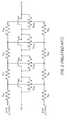
- FIG. 3is a plan view of a first embodiment of a layout for an RF switch 10 that is in accordance with the present disclosure.
- FIG. 3is a plan view of structures that realizes the topology of the related-art RF switch of FIG. 2 without employing metal contacts directly over the drain and source diffusion regions of interior FETs M 2 through MN ⁇ 1.
- the FOMwhich is equal to the RF switch's ON state resistance R ON multiplied by the RF switch's OFF state capacitance C OFF , is greatly improved.
- FIG. 4is a cross-sectional view of the RF switch 10 along a cut-line A-A′ depicted in FIG. 3 .
- the RF switch 10includes a substrate 12 over which a plurality of elongated drain/source (D/S) diffusion regions 14 are laterally disposed in parallel with one another and are separated by a plurality of elongated channel regions 16 .
- the substrate 12is made of a polymeric material such as a thermoplastic or epoxy.
- embodiments of the present disclosureremain functional on typical high-resistance semiconductor substrates such as silicon.
- polymeric materialhas electrical properties that provide superior isolation during operation and prevent harmonics from being generated within the substrate 12 .
- additivessuch as nanopowders may be included in the polymeric material to increase thermal conductivity of the RF switch 10 .
- Semiconductor substratesmay be replaced with polymeric substrates using techniques disclosed in U.S. Patent Publication Nos.
- a plurality of elongated D/S resistor regions 18makes up the source-to-drain resistors R SD1 through R SDN that are depicted in the topologies of FIG. 1 and FIG. 2 .
- Each of the plurality of elongated D/S resistor regions 18extends between an adjacent pair of the plurality of elongated D/S diffusion regions 14 .
- the RF switch 10further includes a plurality of elongated gate structures 20 .
- Each of the plurality of elongated gate structures 20resides over corresponding ones of the plurality of elongated channel regions 16 .
- a gate dielectric layer 22separates the plurality of elongated gate structures 20 from the plurality of elongated channel regions 16 .
- the plurality of elongated gate structures 20is made of polysilicon, and the gate dielectric layer 22 is made of silicon dioxide.
- a silicide layer 24is disposed over a majority of at least top surfaces of the plurality of elongated D/S diffusion regions 14 and the plurality of elongated gate structures 20 , whereas less than a majority of each of the plurality of elongated D/S resistor regions 18 are covered by the silicide layer 24 .
- the silicide layer 24covers 100% of the at least top surfaces of the plurality of the elongated D/S diffusion regions 14 and the plurality of elongated gate structures 20 .
- the silicide layer 24covers between 80% and 90% of the at least top surfaces of the plurality of the elongated D/S diffusion regions 14 and the plurality of elongated gate structures 20 . Moreover, in at least some embodiments, the silicide layer 24 covers between 0% and less than 50% of the plurality of elongated D/S resistor regions 18 .
- the plurality of elongated D/S diffusion regions 14extends from a silicide region 26 into a first non-silicide region 28 .
- the first non-silicide region 28is referred to by some in the semiconductor industry as the silicide block region.
- each of the plurality of elongated D/S resistor regions 18is U-shaped, which allows a portion of each of the plurality of elongated gate structures 20 to extend between corresponding ones of the plurality of elongated D/S resistor regions 18 .
- a plurality of gate contacts 30is disposed over the portion of each of the plurality of elongated gate structures 20 that extends between corresponding ones of the plurality of elongated D/S resistor regions 18 .
- a plurality of shallow trench isolation (STI) regions 32is formed between the extended portions of the plurality of elongated gate structures 20 and an interior of the U-shaped plurality of elongated D/S resistor regions 18 .
- STIshallow trench isolation
- the RF switch 10also includes an elongated source diffusion region 34 having a plurality of source contacts 36 coupled to a first metal trace 38 , which in turn is coupled to a first RF signal terminal RF 1 . Further included is an elongated drain diffusion region 40 having a plurality of drain contacts 42 coupled to a second metal trace 44 , which is coupled to a second RF signal terminal RF 2 .
- the elongated source diffusion region 34 and the elongated drain diffusion region 40both reside in the silicide region 26 and are covered by the silicide layer 24 .
- the elongated source diffusion region 34 , an adjacent one of the plurality of elongated gate structures 20 , and an adjacent one of the plurality of elongated D/S diffusion regions 14make up a first FET M 1 .
- the elongated drain diffusion region 40 , an adjacent one of the plurality of elongated gate structures 20 , and an adjacent one of the plurality of elongated D/S diffusion regions 14make up a last FET MN.
- the remaining plurality of elongated D/S diffusion regions 14 and remaining plurality of elongated gate structures 20make up interior FETs M 2 through MN ⁇ 1.
- the RF switch 10has the benefit of not having typical metallization within the interior of the silicide region 26 between the elongated source diffusion region 34 and the elongated drain diffusion region 40 .
- an ON state resistance R ON and an OFF state capacitance C OFFare significantly reduced, which provides a significantly improved FOM.
- FIG. 3 and FIG. 4is fabricated with silicon-on-insulator (SOI) technology.
- a buried oxide (BOX) layer 46separates the substrate 12 from an active device layer 48 that includes the plurality of elongated D/S diffusion regions 14 and the plurality of elongated D/S resistor regions 18 .
- the plurality of elongated D/S diffusion regions 14 and the plurality of elongated D/S resistor regions 18reside within a common plane.
- the plurality of elongated D/S resistor regions 18forms active well resistors.
- the plurality of elongated D/S resistor regions 18is made of polysilicon.
- each of the plurality of elongated D/S resistor regions 18provides at least between 100 ohms ( ⁇ ) and 10,000 ⁇ of resistance between the adjacent pair of the plurality of elongated D/S diffusion regions 14 . In other exemplary embodiments, each of the plurality of the elongated D/S resistor regions 18 provides at least between 750 ⁇ and 1,250 ⁇ of resistance between the adjacent pair of the plurality of elongated D/S diffusion regions 14 . In particular exemplary embodiments, each of the plurality of elongated D/S resistor regions 18 provides at least 1,000 ⁇ 10% of resistance between the adjacent pair of the plurality of elongated D/S diffusion regions 14 .
- the RF switch 10also includes a plurality of body diffusion regions 50 wherein each of the plurality of body diffusion regions 50 extends between ends of adjacent pairs of the plurality of elongated D/S diffusion regions 14 and is included with the silicide region 26 . As such, in this exemplary embodiment, top surfaces of the plurality of body diffusion regions 50 are covered by the silicide layer 24 .
- the RF switch 10further includes a second non-silicide region 52 that is opposite the first non-silicide region 28 with the silicide region 26 in between.
- a plurality of body resistor regions 54extends between an adjacent pair of the plurality of body diffusion regions 50 and in this exemplary embodiment extends into the second non-silicide region 52 .
- each of the plurality of body resistor regions 54is not covered by the silicide layer 24 in the exemplary embodiment of FIG. 3 . In other embodiments, less than a majority of each of plurality of body resistor regions 54 are covered by the silicide layer 24 . In some exemplary embodiments, each of the plurality of body resistor regions 54 provides at least between 100 ⁇ and 10,000 ⁇ of resistance between the adjacent pair of the plurality of body regions. In other exemplary embodiments, each of the plurality of body resistor regions 54 provides at least between 750 ⁇ and 1,250 ⁇ of resistance between the adjacent pair of the plurality of body diffusion regions 50 .
- each of the plurality of body resistor regions 54provides at least 1,000 ⁇ 10% of resistance between the adjacent pair of the plurality of body diffusion regions 50 .
- the body resistor regions 54comprise active well resistors.
- each of the plurality of body resistor regions 54is U-shaped.
- a plurality of STI regions 56extends within rectangular interiors of the plurality of body resistor regions 54 that are U-shaped. The plurality of body resistor regions 54 makes up the resistors R B1 through R BN depicted in FIG. 2 .
- FIG. 5is a plan view of a second embodiment of an RF switch layout that is in accordance with the present disclosure.
- FIG. 5is a plan view of structures that realizes the topology of the related-art RF switch of FIG. 1 without employing metal contacts directly over the drain and source diffusion regions of interior FETs M 2 through MN ⁇ 1.
- a plurality of body resistor regions 58is coupled between corresponding ones of the plurality of body diffusion regions 50 and a bias node 60 .
- the plurality of body resistor regions 58extends into the second non-silicide region 52 .
- the plurality of body resistor regions 58is not covered by the silicide layer 24 in the exemplary embodiment of FIG. 5 . In other embodiments, less than a majority of each of the plurality of body resistor regions 58 are covered by the silicide layer 24 .
- each of the plurality of body resistor regions 58provides at least between 100 ⁇ and 10,000 ⁇ of resistance between the plurality of body diffusion regions 50 and the bias node 60 . In other exemplary embodiments, each of the plurality of body resistor regions 58 provides at least between 750 ⁇ and 1,250 ⁇ of resistance between the plurality of body diffusion regions 50 and the bias node 60 . In yet other embodiments, each of the plurality of body resistor regions 58 provides at least 1,000 ⁇ 10% of resistance between the plurality of body diffusion regions 50 and the bias node 60 . In exemplary embodiments, the plurality of body resistor regions 58 is formed from active well resistors. In the exemplary embodiment of FIG. 5 , the plurality of body resistor regions 58 is serpentine-shaped.
- FIG. 6is a simplified plan view diagram that illustrates an undesirable aspect of the RF switch 10 that is due to merged drain/source diffusions combined with elimination of inner contacts and inner metallization.
- FIG. 7is a plan view diagram of a layout that restores a desirable aspect ratio for the RF switch 10 in accordance with the present disclosure.
- the RF switch 10may be divided into four sections as designated by three dotted lines and rearranged as shown in FIG. 7 .
- the four sectionscoupled together with river routing using a source metal 62 and a drain metal 64 .
- the plurality of elongated gates structures 20is coupled using a gate metallization that is not shown.
- the plurality of elongated D/S diffusion regions 14is divided into coupled segments such that a width-to-length aspect ratio of the RF switch is between 1:1.5 and 1:3.5.
Landscapes
- Physics & Mathematics (AREA)
- Condensed Matter Physics & Semiconductors (AREA)
- General Physics & Mathematics (AREA)
- Engineering & Computer Science (AREA)
- Computer Hardware Design (AREA)
- Microelectronics & Electronic Packaging (AREA)
- Power Engineering (AREA)
- Geometry (AREA)
- Semiconductor Integrated Circuits (AREA)
- Electronic Switches (AREA)
Abstract
Description
This application claims the benefit of provisional patent application Ser. No. 62/410,965, filed Oct. 21, 2016, the disclosure of which is hereby incorporated herein by reference in its entirety.
Embodiments of the present disclosure relate to semiconductor and silicon-on-insulator technologies and semiconductor-based radio frequency switches, both of which can be used in radio frequency communications circuits.
As technology progresses, wireless communications devices, such as smart phones, wireless capable computers, or the like, are becoming increasingly integrated, feature rich, and complex. Such wireless communications devices rely on semiconductor technologies, such as silicon-based technologies, which are evolving toward smaller circuit geometries, lower power consumption, higher operating speeds, and increased complexity. Complementary metal oxide semiconductor technology is an example of a silicon-based technology. Further, wireless communications devices may need to support multiple communications bands, multiple communications modes, multiple communications protocols, and the like. As such, wireless communications devices may need multiple radio frequency (RF) switches to select between different RF circuits depending on which communications bands, modes, and protocols are in use. Such complex RF systems may place strict linearity, insertion loss, and isolation demands on the RF switches.
In general, RF switches having semiconductor-based switching elements have a trade-off between insertion loss and isolation. RF switches that must handle high power levels require low insertion losses. To achieve low insertion loss and high power handling capability, the size of circuit elements within an RF switch can be relatively large. However, such large circuit elements are associated with relatively large capacitances, which decreases isolation. Further, multiple large capacitances have non-linearities, which degrade linearity of the RF switch. In particular, the performance of an RF switch is in part related to a figure of merit that is equal to the RF switch's ON state resistance RONmultiplied by the RF switch's OFF state capacitance COFF. Thus, there is a need for an RF switch that improves the figure of merit and the trade-off between insertion loss and isolation and has improved linearity performance.
Disclosed is a radio frequency (RF) switch that includes a substrate and a plurality of elongated drain/source (D/S) diffusion regions laterally disposed in parallel with one another and separated by a plurality of elongated channel regions. A plurality of elongated D/S resistor regions extends between an adjacent pair of plurality of elongated D/S diffusion regions, and a plurality of elongated gate structures reside over corresponding ones of the elongated channel regions. A silicide layer resides over a majority of top surfaces of the plurality of the elongated D/S diffusion regions and the plurality of elongated gate structures, wherein less than a majority of each of the plurality of elongated D/S resistor regions is covered by the silicide layer.
In at least one exemplary embodiment, the RF switch further includes a plurality of body regions wherein each of the plurality of the body regions extends between ends of adjacent pairs of the plurality of elongated D/S diffusion regions. A plurality of body resistor regions extends between an adjacent pair of the plurality of body regions.
Those skilled in the art will appreciate the scope of the present disclosure and realize additional aspects thereof after reading the following detailed description of the preferred embodiments in association with the accompanying drawing figures.
The accompanying drawing figures incorporated in and forming a part of this specification illustrate several aspects of the disclosure and, together with the description, serve to explain the principles of the disclosure.
The embodiments set forth below represent the necessary information to enable those skilled in the art to practice the embodiments and illustrate the best mode of practicing the embodiments. Upon reading the following description in light of the accompanying drawing figures, those skilled in the art will understand the concepts of the disclosure and will recognize applications of these concepts not particularly addressed herein. It should be understood that these concepts and applications fall within the scope of the disclosure and the accompanying claims.
It will be understood that, although the terms first, second, etc. may be used herein to describe various elements, these elements should not be limited by these terms. These terms are only used to distinguish one element from another. For example, a first element could be termed a second element, and, similarly, a second element could be termed a first element, without departing from the scope of the present disclosure. As used herein, the term “and/or” includes any and all combinations of one or more of the associated listed items.
It will be understood that when an element such as a layer, region, or substrate is referred to as being “on” or extending “onto” another element, it can be directly on or extend directly onto the other element or intervening elements may also be present. In contrast, when an element is referred to as being “directly on” or extending “directly onto” another element, there are no intervening elements present. Likewise, it will be understood that when an element such as a layer, region, or substrate is referred to as being “over” or extending “over” another element, it can be directly over or extend directly over the other element or intervening elements may also be present. In contrast, when an element is referred to as being “directly over” or extending “directly over” another element, there are no intervening elements present. It will also be understood that when an element is referred to as being “connected” or “coupled” to another element, it can be directly connected or coupled to the other element or intervening elements may be present. In contrast, when an element is referred to as being “directly connected” or “directly coupled” to another element, there are no intervening elements present.
Relative terms such as “below” or “above” or “upper” or “lower” or “horizontal” or “vertical” may be used herein to describe a relationship of one element, layer, or region to another element, layer, or region as illustrated in the Figures. It will be understood that these terms and those discussed above are intended to encompass different orientations of the device in addition to the orientation depicted in the Figures.
The terminology used herein is for the purpose of describing particular embodiments only and is not intended to be limiting of the disclosure. As used herein, the singular forms “a,” “an,” and “the” are intended to include the plural forms as well, unless the context clearly indicates otherwise. It will be further understood that the terms “comprises,” “comprising,” “includes,” and/or “including” when used herein specify the presence of stated features, integers, steps, operations, elements, and/or components, but do not preclude the presence or addition of one or more other features, integers, steps, operations, elements, components, and/or groups thereof.
Unless otherwise defined, all terms (including technical and scientific terms) used herein have the same meaning as commonly understood by one of ordinary skill in the art to which this disclosure belongs. It will be further understood that terms used herein should be interpreted as having a meaning that is consistent with their meaning in the context of this specification and the relevant art and will not be interpreted in an idealized or overly formal sense unless expressly so defined herein.
A first RF signal terminal RF1 is coupled to a drain of the first FET M1 and a second RF signal terminal RF2 is coupled at a source of the Nth FET MN. An RF signal applied to either of the first RF signal terminal RF1 or the second RF signal terminal RF2 is prevented from passing between the first RF signal terminal RF1 and the second RF signal terminal RF2 when the RF switch is in an OFF state. When a ground level or negative potential is applied to the gate control terminal, the FETs M1 through MN that are stacked in series are in the OFF state. In contrast, when a gate voltage that is above a positive threshold voltage (Vth) is applied to the gate control terminal, the FETs M1 through MN are in an ON state. An RF signal applied to either of the first RF signal terminal RF1 or the second RF signal terminal RF2 passes between the first RF signal terminal RF1 and the second RF signal terminal RF2 when each of the FETs M1 through MN is in an ON state. The source-to-drain resistors RSD1through RSDNare coupled across each of the FETs M1 through MN from source to drain to help balance drain-to-source voltages when the FETs M1 through MN are in the OFF state.
Typically, a physical layout for either of the RF switches schematically depicted inFIGS. 1 and 2 requires connections to be made using relatively long and relatively thin metal traces within metal layers referred to in industry as Metal 1 and Metal 2 layers. As such, these metal layers along with contacts and vias are populated among each FET M1 through M2 making up the RF switch. As a result, parasitic resistances and parasitic capacitances due to the metal layers, contacts, and vias accumulate to undesirably high values that are detrimental to the figure of merit (FOM) of the RF switches. For example, the long thin traces of the Metal 1 layer force electrical current traveling horizontally through the long thin traces to encounter a total resistance that is relatively high compared with electrical current flowing vertically through a thicker trace over a shorter distance. Moreover, in a typical layout there are metal contacts directly over diffusion regions making up the drain and source of each of the FETs M1 through MN. Due to close spacing relative to one another, the metal contacts directly over the diffusion regions accumulate a relatively large and undesirable capacitance. The structures of the present disclosure depicted inFIGS. 3, 4 , and5 eliminate the metal contacts directly over the drain and source diffusion regions of interior FETs M2 through MN−1. Moreover, the presently disclosed structures also eliminate traces of the Metal 1 layer that typically carry electrical current to and from the metal contacts directly over the diffusion regions.
A plurality of elongated D/S resistor regions 18 makes up the source-to-drain resistors RSD1through RSDNthat are depicted in the topologies ofFIG. 1 andFIG. 2 . Each of the plurality of elongated D/S resistor regions 18 extends between an adjacent pair of the plurality of elongated D/S diffusion regions 14. TheRF switch 10 further includes a plurality ofelongated gate structures 20. Each of the plurality ofelongated gate structures 20 resides over corresponding ones of the plurality ofelongated channel regions 16. Agate dielectric layer 22 separates the plurality ofelongated gate structures 20 from the plurality ofelongated channel regions 16. In an exemplary embodiment, the plurality ofelongated gate structures 20 is made of polysilicon, and thegate dielectric layer 22 is made of silicon dioxide. Asilicide layer 24 is disposed over a majority of at least top surfaces of the plurality of elongated D/S diffusion regions 14 and the plurality ofelongated gate structures 20, whereas less than a majority of each of the plurality of elongated D/S resistor regions 18 are covered by thesilicide layer 24. In the exemplary embodiment ofFIG. 3 andFIG. 4 , thesilicide layer 24 covers 100% of the at least top surfaces of the plurality of the elongated D/S diffusion regions 14 and the plurality ofelongated gate structures 20. In other exemplary embodiments, thesilicide layer 24 covers between 80% and 90% of the at least top surfaces of the plurality of the elongated D/S diffusion regions 14 and the plurality ofelongated gate structures 20. Moreover, in at least some embodiments, thesilicide layer 24 covers between 0% and less than 50% of the plurality of elongated D/S resistor regions 18.
In the exemplary embodiment ofFIG. 3 andFIG. 4 , the plurality of elongated D/S diffusion regions 14 extends from asilicide region 26 into a firstnon-silicide region 28. The firstnon-silicide region 28 is referred to by some in the semiconductor industry as the silicide block region. As depicted inFIG. 3 , each of the plurality of elongated D/S resistor regions 18 is U-shaped, which allows a portion of each of the plurality ofelongated gate structures 20 to extend between corresponding ones of the plurality of elongated D/S resistor regions 18. A plurality ofgate contacts 30, one for each of the plurality ofelongated gate structures 20, is disposed over the portion of each of the plurality ofelongated gate structures 20 that extends between corresponding ones of the plurality of elongated D/S resistor regions 18. Moreover, in the exemplary embodiment ofFIG. 3 , a plurality of shallow trench isolation (STI)regions 32 is formed between the extended portions of the plurality ofelongated gate structures 20 and an interior of the U-shaped plurality of elongated D/S resistor regions 18.
TheRF switch 10 also includes an elongatedsource diffusion region 34 having a plurality ofsource contacts 36 coupled to afirst metal trace 38, which in turn is coupled to a first RF signal terminal RF1. Further included is an elongateddrain diffusion region 40 having a plurality ofdrain contacts 42 coupled to asecond metal trace 44, which is coupled to a second RF signal terminal RF2. In the exemplary embodiment ofFIG. 3 , the elongatedsource diffusion region 34 and the elongateddrain diffusion region 40 both reside in thesilicide region 26 and are covered by thesilicide layer 24. The elongatedsource diffusion region 34, an adjacent one of the plurality ofelongated gate structures 20, and an adjacent one of the plurality of elongated D/S diffusion regions 14 make up a first FET M1. The elongateddrain diffusion region 40, an adjacent one of the plurality ofelongated gate structures 20, and an adjacent one of the plurality of elongated D/S diffusion regions 14 make up a last FET MN. The remaining plurality of elongated D/S diffusion regions 14 and remaining plurality ofelongated gate structures 20 make up interior FETs M2 through MN−1.
In particular reference toFIG. 4 , note that there are no metal contacts directly over the plurality of elongated D/S diffusion regions 14 that are coupled to thesilicide layer 24. Thus, theRF switch 10 has the benefit of not having typical metallization within the interior of thesilicide region 26 between the elongatedsource diffusion region 34 and the elongateddrain diffusion region 40. As a result of this lack of metallization, an ON state resistance RONand an OFF state capacitance COFFare significantly reduced, which provides a significantly improved FOM.
The exemplary embodiment ofFIG. 3 andFIG. 4 is fabricated with silicon-on-insulator (SOI) technology. As such, a buried oxide (BOX)layer 46 separates thesubstrate 12 from anactive device layer 48 that includes the plurality of elongated D/S diffusion regions 14 and the plurality of elongated D/S resistor regions 18. As such, the plurality of elongated D/S diffusion regions 14 and the plurality of elongated D/S resistor regions 18 reside within a common plane. Moreover, the plurality of elongated D/S resistor regions 18 forms active well resistors. In at least one exemplary embodiment, the plurality of elongated D/S resistor regions 18 is made of polysilicon.
In exemplary embodiments, each of the plurality of elongated D/S resistor regions 18 provides at least between 100 ohms (Ω) and 10,000Ω of resistance between the adjacent pair of the plurality of elongated D/S diffusion regions 14. In other exemplary embodiments, each of the plurality of the elongated D/S resistor regions 18 provides at least between 750Ω and 1,250Ω of resistance between the adjacent pair of the plurality of elongated D/S diffusion regions 14. In particular exemplary embodiments, each of the plurality of elongated D/S resistor regions 18 provides at least 1,000Ω±10% of resistance between the adjacent pair of the plurality of elongated D/S diffusion regions 14.
As best seen inFIG. 3 , theRF switch 10 also includes a plurality of body diffusion regions50 wherein each of the plurality of body diffusion regions50 extends between ends of adjacent pairs of the plurality of elongated D/S diffusion regions 14 and is included with thesilicide region 26. As such, in this exemplary embodiment, top surfaces of the plurality of body diffusion regions50 are covered by thesilicide layer 24. TheRF switch 10 further includes a secondnon-silicide region 52 that is opposite the firstnon-silicide region 28 with thesilicide region 26 in between. A plurality ofbody resistor regions 54 extends between an adjacent pair of the plurality of body diffusion regions50 and in this exemplary embodiment extends into the secondnon-silicide region 52. As such, the plurality ofbody resistor regions 54 is not covered by thesilicide layer 24 in the exemplary embodiment ofFIG. 3 . In other embodiments, less than a majority of each of plurality ofbody resistor regions 54 are covered by thesilicide layer 24. In some exemplary embodiments, each of the plurality ofbody resistor regions 54 provides at least between 100Ω and 10,000Ω of resistance between the adjacent pair of the plurality of body regions. In other exemplary embodiments, each of the plurality ofbody resistor regions 54 provides at least between 750Ω and 1,250Ω of resistance between the adjacent pair of the plurality of body diffusion regions50. In yet other embodiments, each of the plurality ofbody resistor regions 54 provides at least 1,000Ω±10% of resistance between the adjacent pair of the plurality of body diffusion regions50. In exemplary embodiments, thebody resistor regions 54 comprise active well resistors. In the exemplary embodiment ofFIG. 3 , each of the plurality ofbody resistor regions 54 is U-shaped. A plurality ofSTI regions 56 extends within rectangular interiors of the plurality ofbody resistor regions 54 that are U-shaped. The plurality ofbody resistor regions 54 makes up the resistors RB1through RBNdepicted inFIG. 2 .
In some exemplary embodiments, each of the plurality ofbody resistor regions 58 provides at least between 100Ω and 10,000Ω of resistance between the plurality of body diffusion regions50 and thebias node 60. In other exemplary embodiments, each of the plurality ofbody resistor regions 58 provides at least between 750Ω and 1,250Ω of resistance between the plurality of body diffusion regions50 and thebias node 60. In yet other embodiments, each of the plurality ofbody resistor regions 58 provides at least 1,000Ω±10% of resistance between the plurality of body diffusion regions50 and thebias node 60. In exemplary embodiments, the plurality ofbody resistor regions 58 is formed from active well resistors. In the exemplary embodiment ofFIG. 5 , the plurality ofbody resistor regions 58 is serpentine-shaped.
Those skilled in the art will recognize improvements and modifications to the preferred embodiments of the present disclosure. All such improvements and modifications are considered within the scope of the concepts disclosed herein and the claims that follow.
Claims (23)
1. A radio frequency (RF) switch comprising:
a substrate;
a plurality of elongated drain/source (D/S) diffusion regions laterally disposed in parallel with one another and separated by a plurality of elongated channel regions;
a plurality of elongated D/S resistor regions wherein each of the plurality of elongated D/S resistor regions extends between an adjacent pair of the plurality of elongated D/S diffusion regions;
a plurality of elongated gate structures wherein each of the plurality of elongated gate structures resides over corresponding ones of the plurality of elongated channel regions; and
a silicide layer over a majority of at least top surfaces of the plurality of elongated D/S diffusion regions and the plurality of elongated gate structures, wherein less than a majority of each of the plurality of elongated D/S resistor regions are covered by the silicide layer.
2. The RF switch ofclaim 1 wherein the plurality of elongated D/S diffusion regions and the plurality of elongated D/S resistor regions reside within a common plane.
3. The RF switch ofclaim 1 wherein the silicide layer covers between 80% and 90% of the at least top surfaces of the plurality of elongated D/S diffusion regions and the plurality of elongated gate structures.
4. The RF switch ofclaim 1 wherein the silicide layer covers 100% of the at least top surfaces of the plurality of the elongated D/S diffusion regions and the plurality of elongated gate structures.
5. The RF switch ofclaim 1 wherein the silicide layer covers between 0% and less than 50% of the plurality of elongated D/S resistor regions.
6. The RF switch ofclaim 1 wherein each of the plurality of elongated D/S resistor regions provides at least between 100 ohms (Ω) and 10,000Ω of resistance between the adjacent pair of the plurality of elongated D/S diffusion regions.
7. The RF switch ofclaim 1 wherein each of the plurality of elongated D/S resistor regions provides at least between 750Ω and 1,250Ω of resistance between the adjacent pair of the plurality of elongated D/S diffusion regions.
8. The RF switch ofclaim 1 wherein each of the plurality of elongated D/S resistor regions provides at least 1,000Ω±10% of resistance between the adjacent pair of the plurality of elongated D/S diffusion regions.
9. The RF switch ofclaim 1 wherein the plurality of elongated D/S resistor regions comprises active well resistors.
10. The RF switch ofclaim 9 wherein the plurality of elongated gate structures includes gate contacts that reside between the plurality of elongated D/S resistor regions.
11. The RF switch ofclaim 1 wherein each of the plurality of elongated D/S resistor regions is U-shaped.
12. The RF switch ofclaim 1 wherein the substrate is made of a polymeric material.
13. The RF switch ofclaim 1 wherein there are no metal contacts directly over the plurality of elongated D/S diffusion regions that are coupled to the silicide layer.
14. The RF switch ofclaim 1 further including a buried oxide (BOX) layer sandwiched between the substrate and the plurality of elongated D/S diffusion regions.
15. The RF switch ofclaim 1 further comprising:
a plurality of body regions wherein each of the plurality of body regions extends between ends of adjacent pairs of the plurality of elongated D/S diffusion regions; and
a plurality of body resistor regions, wherein each of the plurality of body resistor regions extends between an adjacent pair of the plurality of body regions.
16. The RF switch ofclaim 15 wherein each of the plurality of body resistor regions provides at least between 100Ω and 10,000Ω of resistance between the adjacent pair of the plurality of body regions.
17. The RF switch ofclaim 15 wherein each of the plurality of body resistor regions provides at least between 750Ω and 1,250Ω of resistance between the adjacent pair of the plurality of body diffusion regions.
18. The RF switch ofclaim 15 wherein each of the plurality of body resistor regions provides at least 1,000Ω±10% of resistance between the adjacent pair of the plurality of body diffusion regions.
19. The RF switch ofclaim 15 wherein the plurality of body resistor regions comprises active well resistors.
20. The RF switch ofclaim 15 wherein each of the plurality of body resistor regions is U-shaped.
21. The RF switch ofclaim 15 wherein plurality of elongated D/S diffusion regions is divided into coupled segments such that a width-to-length aspect ratio of the RF switch is between 1:1.5 and 1:3.5.
22. The RF switch ofclaim 1 further comprising:
a plurality of body regions wherein each of the plurality of body regions extends between ends of adjacent pairs of the plurality of elongated D/S diffusion regions; and
a plurality of body resistor regions, wherein each of the plurality of body resistor regions extends between a bias node and corresponding ones of the plurality of body regions.
23. The RF switch ofclaim 22 wherein each of the plurality of body resistors is serpentine-shaped.
Priority Applications (1)
| Application Number | Priority Date | Filing Date | Title |
|---|---|---|---|
| US15/789,107US10090339B2 (en) | 2016-10-21 | 2017-10-20 | Radio frequency (RF) switch |
Applications Claiming Priority (2)
| Application Number | Priority Date | Filing Date | Title |
|---|---|---|---|
| US201662410965P | 2016-10-21 | 2016-10-21 | |
| US15/789,107US10090339B2 (en) | 2016-10-21 | 2017-10-20 | Radio frequency (RF) switch |
Publications (2)
| Publication Number | Publication Date |
|---|---|
| US20180114801A1 US20180114801A1 (en) | 2018-04-26 |
| US10090339B2true US10090339B2 (en) | 2018-10-02 |
Family
ID=61969899
Family Applications (1)
| Application Number | Title | Priority Date | Filing Date |
|---|---|---|---|
| US15/789,107ActiveUS10090339B2 (en) | 2016-10-21 | 2017-10-20 | Radio frequency (RF) switch |
Country Status (1)
| Country | Link |
|---|---|
| US (1) | US10090339B2 (en) |
Cited By (2)
| Publication number | Priority date | Publication date | Assignee | Title |
|---|---|---|---|---|
| US11418183B2 (en)* | 2018-03-28 | 2022-08-16 | Psemi Corporation | AC coupling modules for bias ladders |
| US11863227B2 (en) | 2021-10-25 | 2024-01-02 | Analog Devices International Unlimited Company | Radio frequency switches with fast switching speed |
Families Citing this family (16)
| Publication number | Priority date | Publication date | Assignee | Title |
|---|---|---|---|---|
| US9024700B2 (en) | 2008-02-28 | 2015-05-05 | Peregrine Semiconductor Corporation | Method and apparatus for use in digitally tuning a capacitor in an integrated circuit device |
| US9948281B2 (en) | 2016-09-02 | 2018-04-17 | Peregrine Semiconductor Corporation | Positive logic digitally tunable capacitor |
| US10672885B2 (en)* | 2017-10-19 | 2020-06-02 | Newport Fab, Llc | Silicide block isolation for reducing off-capacitance of a radio frequency (RF) switch |
| US10325833B1 (en) | 2018-02-20 | 2019-06-18 | Newport Fab, Llc | Bent polysilicon gate structure for small footprint radio frequency (RF) switch |
| US10586870B2 (en) | 2018-02-20 | 2020-03-10 | Newport Fab, Llc | Wide contact structure for small footprint radio frequency (RF) switch |
| US10886911B2 (en) | 2018-03-28 | 2021-01-05 | Psemi Corporation | Stacked FET switch bias ladders |
| US10505530B2 (en)* | 2018-03-28 | 2019-12-10 | Psemi Corporation | Positive logic switch with selectable DC blocking circuit |
| US10523195B1 (en) | 2018-08-02 | 2019-12-31 | Psemi Corporation | Mixed style bias network for RF switch FET stacks |
| US11430749B2 (en)* | 2018-10-31 | 2022-08-30 | Infineon Technologies Ag | ESD protection in an electronic device |
| US10707866B1 (en)* | 2018-12-21 | 2020-07-07 | Qualcomm Incorporated | Capacitance balance in dual sided contact switch |
| TWI747292B (en)* | 2019-07-12 | 2021-11-21 | 台灣積體電路製造股份有限公司 | Semiconductor device |
| US11296688B2 (en) | 2019-12-18 | 2022-04-05 | Skyworks Solutions, Inc. | Switching time reduction of an RF switch |
| US11476849B2 (en) | 2020-01-06 | 2022-10-18 | Psemi Corporation | High power positive logic switch |
| US12160229B2 (en) | 2021-12-28 | 2024-12-03 | Skyworks Solutions, Inc. | Switching time reduction of an RF switch |
| US12199594B2 (en) | 2022-01-06 | 2025-01-14 | Skyworks Solutions, Inc. | Switching time reduction of an RF switch |
| US20250185376A1 (en)* | 2023-12-01 | 2025-06-05 | Globalfoundries U.S. Inc. | Fully depleted semiconductor-on-insulator switch with built-in electrostatic discharge protection |
Citations (173)
| Publication number | Priority date | Publication date | Assignee | Title |
|---|---|---|---|---|
| US4093562A (en) | 1976-02-20 | 1978-06-06 | Matsushita Electric Industrial Co., Ltd. | Polymeric compositions for manufacture of secondary electron multiplier tubes and method for manufacture thereof |
| US4366202A (en) | 1981-06-19 | 1982-12-28 | Kimberly-Clark Corporation | Ceramic/organic web |
| US5061663A (en) | 1986-09-04 | 1991-10-29 | E. I. Du Pont De Nemours And Company | AlN and AlN-containing composites |
| US5069626A (en) | 1987-07-01 | 1991-12-03 | Western Digital Corporation | Plated plastic castellated interconnect for electrical components |
| US5391257A (en) | 1993-12-10 | 1995-02-21 | Rockwell International Corporation | Method of transferring a thin film to an alternate substrate |
| US5459368A (en) | 1993-08-06 | 1995-10-17 | Matsushita Electric Industrial Co., Ltd. | Surface acoustic wave device mounted module |
| US5646432A (en) | 1992-05-14 | 1997-07-08 | Seiko Instruments Inc. | Semiconductor thin film formed on a supporting substrate |
| US5648013A (en) | 1992-12-24 | 1997-07-15 | Canon Kabushiki Kaisha | Plastic additive, plastic composition containing the additive and plastic molding containing the additive |
| US5699027A (en) | 1995-03-28 | 1997-12-16 | Matsushita Electric Industrial Co., Ltd. | Surface acoustic wave devices having a guard layer |
| US5709960A (en) | 1996-06-21 | 1998-01-20 | Motorola, Inc. | Mold compound |
| US5831369A (en) | 1994-05-02 | 1998-11-03 | Siemens Matsushita Components Gmbh & Co. Kg | Encapsulation for electronic components and method for producing the encapsulation |
| US5920142A (en) | 1996-03-08 | 1999-07-06 | Matsushita Electric Industrial Co., Ltd. | Electronic part and a method of production thereof |
| US6072557A (en) | 1998-07-31 | 2000-06-06 | Sharp Kabushiki Kaisha | Color liquid crystal display apparatus and method for producing the same |
| US6084284A (en) | 1994-11-18 | 2000-07-04 | Adamic, Jr.; Fred W. | Integrated circuit including inverted dielectric isolation |
| US6154366A (en) | 1999-11-23 | 2000-11-28 | Intel Corporation | Structures and processes for fabricating moisture resistant chip-on-flex packages |
| US6154372A (en) | 1993-09-02 | 2000-11-28 | Siemens Aktiengesellschaft | Multichip module for surface mounting on printed circuit boards |
| US6236061B1 (en) | 1999-01-08 | 2001-05-22 | Lakshaman Mahinda Walpita | Semiconductor crystallization on composite polymer substrates |
| US6235554B1 (en) | 1995-11-27 | 2001-05-22 | Micron Technology, Inc. | Method for fabricating stackable chip scale semiconductor package |
| US20010004131A1 (en) | 1999-12-17 | 2001-06-21 | Tobita Masayuki | Adhesion method and electronic component |
| US6268654B1 (en) | 1997-04-18 | 2001-07-31 | Ankor Technology, Inc. | Integrated circuit package having adhesive bead supporting planar lid above planar substrate |
| US6271469B1 (en) | 1999-11-12 | 2001-08-07 | Intel Corporation | Direct build-up layer on an encapsulated die package |
| US20020070443A1 (en) | 2000-12-08 | 2002-06-13 | Xiao-Chun Mu | Microelectronic package having an integrated heat sink and build-up layers |
| US20020074641A1 (en) | 2000-12-15 | 2002-06-20 | Steven Towle | Microelectronic package having a bumpless laminated interconnection layer |
| US6423570B1 (en) | 2000-10-18 | 2002-07-23 | Intel Corporation | Method to protect an encapsulated die package during back grinding with a solder metallization layer and devices formed thereby |
| US6426559B1 (en) | 2000-06-29 | 2002-07-30 | National Semiconductor Corporation | Miniature 3D multi-chip module |
| US20020137263A1 (en) | 2001-03-26 | 2002-09-26 | Steven Towle | Dispensing process for fabrication of microelectronic packages |
| US20020185675A1 (en) | 2001-06-06 | 2002-12-12 | International Business Machines Corporation | SOI device with reduced junction capacitance |
| US6578458B1 (en) | 1996-11-12 | 2003-06-17 | Micron Technology, Inc. | Method for sawing wafers employing multiple indexing techniques for multiple die dimensions |
| US20030207515A1 (en) | 2002-01-09 | 2003-11-06 | Micron Technology, Inc., Boise, Id | Stacked die in die BGA package |
| US6713859B1 (en) | 2000-09-13 | 2004-03-30 | Intel Corporation | Direct build-up layer on an encapsulated die package having a moisture barrier structure |
| US20040166642A1 (en) | 2003-02-20 | 2004-08-26 | Hao-Yu Chen | Semiconductor nano-rod devices |
| US20040164367A1 (en) | 2003-02-21 | 2004-08-26 | Jae-Yeong Park | Duplexer filter having film bulk acoustic resonator and semiconductor package thereof |
| US20040219765A1 (en) | 2002-12-31 | 2004-11-04 | Rafael Reif | Method of forming a multi-layer semiconductor structure incorporating a processing handle member |
| US6841413B2 (en) | 2002-01-07 | 2005-01-11 | Intel Corporation | Thinned die integrated circuit package |
| US20050037595A1 (en) | 2003-08-11 | 2005-02-17 | Sumitomo Electric Industries, Ltd | Method of recovering and reproducing substrates and method of producing semiconductor wafers |
| US6864156B1 (en) | 2003-04-04 | 2005-03-08 | Xilinx, Inc. | Semiconductor wafer with well contacts on back side |
| US20050079686A1 (en) | 2002-02-19 | 2005-04-14 | Infineon Technologies Ag | Method for producing a cover, method for producing a packaged device |
| US6943429B1 (en) | 2001-03-08 | 2005-09-13 | Amkor Technology, Inc. | Wafer having alignment marks extending from a first to a second surface of the wafer |
| US20050212419A1 (en) | 2004-03-23 | 2005-09-29 | Eastman Kodak Company | Encapsulating oled devices |
| JP2006005025A (en) | 2004-06-15 | 2006-01-05 | Sharp Corp | Manufacturing method of semiconductor wafer provided with lid and manufacturing method of semiconductor device |
| US6992400B2 (en) | 2004-01-30 | 2006-01-31 | Nokia Corporation | Encapsulated electronics device with improved heat dissipation |
| US20060057782A1 (en) | 2004-09-14 | 2006-03-16 | Stmicroelectronics Sa | Thin glass chip for an electronic component and manufacturing method |
| US7042072B1 (en) | 2002-08-02 | 2006-05-09 | Amkor Technology, Inc. | Semiconductor package and method of manufacturing the same which reduces warpage |
| US20060105496A1 (en) | 2004-11-16 | 2006-05-18 | Chen Howard H | Device and method for fabricating double-sided SOI wafer scale package with through via connections |
| US7049692B2 (en) | 2003-03-11 | 2006-05-23 | Fujitsu Limited | Stacked semiconductor device |
| US20060108585A1 (en) | 2004-11-22 | 2006-05-25 | Au Optronics Corp. | Thin film transistors and fabrication methods thereof |
| US7109635B1 (en) | 2003-06-11 | 2006-09-19 | Sawtek, Inc. | Wafer level packaging of materials with different coefficients of thermal expansion |
| US20060261446A1 (en) | 2005-05-19 | 2006-11-23 | Micron Technology, Inc. | Backside method and system for fabricating semiconductor components with conductive interconnects |
| US20070020807A1 (en) | 2004-11-09 | 2007-01-25 | Geefay Frank S | Protective structures and methods of fabricating protective structures over wafers |
| US7183172B2 (en) | 2002-05-22 | 2007-02-27 | Samsung Electronics Co., Ltd. | Method of forming silicon-on-insulator (SOI) semiconductor substrate and SOI semiconductor substrate formed thereby |
| US20070069393A1 (en) | 2003-07-24 | 2007-03-29 | Toshiyuki Asahi | Wiring board embedded with spherical semiconductor element |
| US20070075317A1 (en) | 2005-09-30 | 2007-04-05 | Seiko Epson Corporation | Semiconductor device and semiconductor device manufacturing method |
| US20070121326A1 (en) | 2005-11-29 | 2007-05-31 | Gelcore, Llc | LED lighting assemblies with thermal overmolding |
| WO2007074651A1 (en) | 2005-12-26 | 2007-07-05 | Sharp Kabushiki Kaisha | Solid state imaging element module fabrication method |
| US20070158746A1 (en)* | 2006-01-12 | 2007-07-12 | Tatsuya Ohguro | Semiconductor device having SOI substrate |
| US20070181992A1 (en) | 2006-02-06 | 2007-08-09 | Micron Technology, Inc. | Microelectronic devices and methods for manufacturing microelectronic devices |
| US20070190747A1 (en) | 2006-01-23 | 2007-08-16 | Tessera Technologies Hungary Kft. | Wafer level packaging to lidded chips |
| JP2007227439A (en) | 2006-02-21 | 2007-09-06 | Denso Corp | Method and apparatus of manufacturing semiconductor device |
| US20070252481A1 (en) | 2005-06-16 | 2007-11-01 | Murata Manufacturing Co., Ltd. | Piezoelectric device and method for producing same |
| US20070276092A1 (en) | 2003-12-25 | 2007-11-29 | Jsr Corporation | Thermoplastic Elastomer Composition, Method for Producing Same and Formed Article |
| US20080050901A1 (en) | 2006-08-23 | 2008-02-28 | Micron Technology, Inc. | Packaged microelectronic devices and methods for manufacturing packaged microelectronic devices |
| US20080050852A1 (en) | 2006-08-23 | 2008-02-28 | Tae-Hyung Hwang | Manufacturing of flexible display device panel |
| US20080164528A1 (en) | 2007-01-10 | 2008-07-10 | International Business Machines Corporation | Self-aligned metal-semiconductor alloy and metallization for sub-lithographic source and drain contacts |
| JP2008235490A (en) | 2007-03-19 | 2008-10-02 | Sumitomo Bakelite Co Ltd | Hollow structure and manufacturing method therefor |
| US20080272497A1 (en) | 2007-05-04 | 2008-11-06 | Micron Technology, Inc. | Methods of forming conductive vias through substrates, and structures and assemblies resulting therefrom |
| JP2008279567A (en) | 2007-05-11 | 2008-11-20 | Denso Corp | Manufacturing method of semi-conductor apparatus |
| US20080315372A1 (en) | 2007-06-20 | 2008-12-25 | Stats Chippac, Ltd. | Wafer Level Integration Package |
| US20090008714A1 (en) | 2007-07-06 | 2009-01-08 | Hee-Il Chae | Semiconductor devices and methods of forming the same |
| US20090010056A1 (en) | 2002-11-20 | 2009-01-08 | The Regents Of The University Of California | Method and apparatus for capacitorless double-gate storage |
| US20090014856A1 (en) | 2007-07-10 | 2009-01-15 | International Business Machine Corporation | Microbump seal |
| JP2009026880A (en) | 2007-07-18 | 2009-02-05 | Denso Corp | Method of manufacturing semiconductor apparatus |
| US20090179266A1 (en) | 2008-01-11 | 2009-07-16 | International Business Machines Corporation | Device structures for a metal-oxide-semiconductor field effect transistor and methods of fabricating such device structures |
| JP2009530823A (en) | 2006-03-17 | 2009-08-27 | マイクロケム コーポレイション | MEMS device packaging |
| US7596849B1 (en) | 2003-06-11 | 2009-10-06 | Triquint Semiconductor, Inc. | Method of assembling a wafer-level package filter |
| US7619347B1 (en) | 2005-05-24 | 2009-11-17 | Rf Micro Devices, Inc. | Layer acoustic wave device and method of making the same |
| US20100012354A1 (en) | 2008-07-14 | 2010-01-21 | Logan Brook Hedin | Thermally conductive polymer based printed circuit board |
| US20100029045A1 (en) | 2008-08-01 | 2010-02-04 | Freescale Semiconductor, Inc. | Packaging an integrated circuit die with backside metallization |
| US20100045145A1 (en) | 2008-08-19 | 2010-02-25 | Nihon Dempa Kogyo Co., Ltd. | Piezoelectric component and manufacturing method thereof |
| US20100081232A1 (en) | 2007-05-10 | 2010-04-01 | International Business Machines Corporation | Layer transfer process and functionally enhanced integrated circuits produced thereby |
| US20100081237A1 (en) | 2008-09-30 | 2010-04-01 | Avago Technologies Fiber Ip (Singapore) Pte. Ltd. | Integrated Circuit Assemblies and Methods for Encapsulating a Semiconductor Device |
| US20100109122A1 (en) | 2008-11-05 | 2010-05-06 | Stmicroelectronics Inc. | Method to reduce metal fuse thickness without extra mask |
| US7714535B2 (en) | 2006-07-28 | 2010-05-11 | Semiconductor Energy Laboratory Co., Ltd. | Power storage device |
| US20100127340A1 (en) | 2008-11-21 | 2010-05-27 | Kabushiki Kaisha Toshiba | Mems package and method of manufacturing the mems package |
| US20100173436A1 (en) | 2009-01-05 | 2010-07-08 | Dalsa Semiconductor Inc. | Method of making biomems devices |
| US20100200919A1 (en) | 2009-02-06 | 2010-08-12 | Sony Corporation | Semiconductor device |
| US20110003433A1 (en) | 2009-07-01 | 2011-01-06 | Shinko Electric Industries Co., Ltd. | Manufacturing method of semiconductor device |
| US7868419B1 (en) | 2007-10-18 | 2011-01-11 | Rf Micro Devices, Inc. | Linearity improvements of semiconductor substrate based radio frequency devices |
| US20110026232A1 (en) | 2009-07-30 | 2011-02-03 | Megica Corporation | System-in packages |
| US20110036400A1 (en) | 2009-08-17 | 2011-02-17 | First Solar, Inc. | Barrier layer |
| US20110062549A1 (en) | 2009-09-11 | 2011-03-17 | Stats Chippac, Ltd. | Semiconductor Device and Method of Forming Integrated Passive Device |
| US20110068433A1 (en) | 2009-09-24 | 2011-03-24 | Qualcomm Incorporated | Forming radio frequency integrated circuits |
| US20110102002A1 (en) | 2008-04-09 | 2011-05-05 | Riehl Bill L | Electrode and sensor having carbon nanostructures |
| US7960218B2 (en) | 2006-09-08 | 2011-06-14 | Wisconsin Alumni Research Foundation | Method for fabricating high-speed thin-film transistors |
| US20110171792A1 (en) | 2010-01-08 | 2011-07-14 | International Business Machines Corporation | Back-gated fully depleted soi transistor |
| US20110272824A1 (en) | 2010-05-04 | 2011-11-10 | Stats Chippac, Ltd. | Semiconductor Device and Method of Forming Channels in Back Surface of FO-WLCSP for Heat Dissipation |
| US20110272800A1 (en) | 2010-05-10 | 2011-11-10 | Shinko Electric Industries Co,Ltd. | Semiconductor package and method of manufacturing same |
| US20110294244A1 (en) | 2010-05-26 | 2011-12-01 | Panasonic Liquid Crystal Display Co., Ltd. | Method for manufacturing display device |
| US20120003813A1 (en) | 2010-06-30 | 2012-01-05 | Ta Ko Chuang | Oxygen plasma conversion process for preparing a surface for bonding |
| US20120068276A1 (en) | 2010-09-21 | 2012-03-22 | Taiwan Semiconductor Manufacturing Company, Ltd. | Microstructure with an enhanced anchor |
| US20120094418A1 (en) | 2010-10-18 | 2012-04-19 | Triquint Semiconductor, Inc. | Wafer Level Package and Manufacturing Method Using Photodefinable Polymer for Enclosing Acoustic Devices |
| US20120098074A1 (en) | 2010-10-21 | 2012-04-26 | Taiwan Semiconductor Manufacturing Company, Ltd. | Mems device with release aperture |
| US20120104495A1 (en) | 2010-10-27 | 2012-05-03 | Institute of Microelectronics, Chinese Academy of Sciences | Semiconductor structure and method for manufacturing the same |
| US20120119346A1 (en) | 2010-11-17 | 2012-05-17 | Yunhyeok Im | Semiconductor package and method of forming the same |
| US20120153393A1 (en) | 2010-12-17 | 2012-06-21 | Institute of Microelectronics, Chinese Academy of Sciences | Transistor, Semiconductor Device Comprising the Transistor and Method for Manufacturing the Same |
| US20120168863A1 (en) | 2010-12-31 | 2012-07-05 | Institute of Microelectronics, Chinese Academy of Sciences | Semiconductor Structure and Method for Manufacturing the Same |
| US20120256260A1 (en) | 2011-04-08 | 2012-10-11 | International Business Machines Corporation | Dual-depth self-aligned isolation structure for a back gate electrode |
| US20120292700A1 (en) | 2011-05-16 | 2012-11-22 | International Business Machines Corporation | Extremely Thin Semiconductor-On-Insulator (ETSOI) FET With A Back Gate and Reduced Parasitic Capacitance And Method of Forming The Same |
| US20120299105A1 (en) | 2011-05-24 | 2012-11-29 | International Business Machines Corporation | ETSOI CMOS with Back Gates |
| US20130001665A1 (en) | 2011-06-23 | 2013-01-03 | Huilong Zhu | Mosfet and method for manufacturing the same |
| US20130015429A1 (en) | 2011-07-12 | 2013-01-17 | The Regents Of The University Of California | All graphene flash memory device |
| US20130049205A1 (en) | 2011-08-25 | 2013-02-28 | Intel Mobile Communications GmbH | Semiconductor Device and Method of Manufacturing a Semiconductor Device Including Grinding Steps |
| US8420447B2 (en) | 2011-03-23 | 2013-04-16 | Stats Chippac Ltd. | Integrated circuit packaging system with flipchip leadframe and method of manufacture thereof |
| US20130099315A1 (en) | 2011-09-16 | 2013-04-25 | Huilong Zhu | Mosfet and method for manufacturing the same |
| US20130105966A1 (en) | 2011-10-26 | 2013-05-02 | Maxim Integrated Products, Inc. | Three-dimensional chip-to-wafer integration |
| US20130147009A1 (en) | 2011-12-08 | 2013-06-13 | SK Hynix Inc. | Semiconductor device and method for manufacturing the same |
| US20130196483A1 (en) | 2012-01-26 | 2013-08-01 | International Business Machines Corporation | Soi structures including a buried boron nitride dielectric |
| US20130200456A1 (en) | 2011-09-07 | 2013-08-08 | Huilong Zhu | Semiconductor Substrate, Integrated Circuit Having the Semiconductor Substrate, and Methods of Manufacturing the Same |
| US20130280826A1 (en) | 2010-02-16 | 2013-10-24 | Deca Technologies Inc. | Adaptive patterning for panelized packaging |
| US20130299871A1 (en) | 2012-05-14 | 2013-11-14 | Anton Mauder | Lateral transistor on polymer |
| US8643148B2 (en) | 2011-11-30 | 2014-02-04 | Taiwan Semiconductor Manufacturing Company, Ltd. | Chip-on-Wafer structures and methods for forming the same |
| US20140035129A1 (en) | 2009-07-15 | 2014-02-06 | Io Semiconductor, Inc. | Thin integrated circuit chip-on-board assembly and method of making |
| US8658475B1 (en) | 2009-07-29 | 2014-02-25 | Rf Micro Devices, Inc. | Stacked body-contacted field effect transistor |
| US8664044B2 (en) | 2011-11-02 | 2014-03-04 | Stmicroelectronics Pte Ltd. | Method of fabricating land grid array semiconductor package |
| US20140134803A1 (en) | 2012-11-15 | 2014-05-15 | Michael G. Kelly | Method And System For A Semiconductor Device Package With A Die-To-Die First Bond |
| CN103811474A (en) | 2012-11-07 | 2014-05-21 | 索尼公司 | Semiconductor device, method of manufacturing semiconductor device, and antenna switch module |
| US20140168014A1 (en) | 2012-12-13 | 2014-06-19 | Taiwan Semiconductor Manufacturing Company, Ltd. | Antenna Apparatus and Method |
| US20140197530A1 (en) | 2013-01-11 | 2014-07-17 | Intel Mobile Communications GmbH | Semiconductor device with chip having low-k-layers |
| US8791532B2 (en) | 2009-11-18 | 2014-07-29 | Sensirion Ag | Sensor mounted in flip-chip technology on a substrate |
| US20140210314A1 (en) | 2007-08-31 | 2014-07-31 | Rf Micro Devices, Inc. | Mems vibrating structure using an orientation dependent single-crystal piezoelectric thin film layer |
| US8802495B2 (en) | 2012-08-03 | 2014-08-12 | Samsung Electronics Co., Ltd. | Semiconductor packages, methods of manufacturing the same, and semiconductor package structures including the same |
| US8816407B2 (en) | 2012-02-28 | 2014-08-26 | Samsung Electronics Co., Ltd. | Semiconductor package |
| US20140252566A1 (en) | 2013-03-06 | 2014-09-11 | Rf Micro Devices, Inc. | Silicon-on-dual plastic (sodp) technology and methods of manufacturing the same |
| US20140252567A1 (en) | 2013-03-06 | 2014-09-11 | Rf Micro Devices, Inc. | Patterned silicon-on-plastic (sop) technology and methods of manufacturing the same |
| US20140264818A1 (en) | 2013-03-15 | 2014-09-18 | Randall D. Lowe, JR. | Polymer thermal interface material having enhanced thermal conductivity |
| US20140264813A1 (en) | 2013-03-13 | 2014-09-18 | Taiwan Semiconductor Manufacturing Company, Ltd. | Semiconductor Device Package and Method |
| US20140306324A1 (en) | 2013-03-06 | 2014-10-16 | Rf Micro Devices, Inc. | Semiconductor device with a polymer substrate and methods of manufacturing the same |
| US20140327150A1 (en) | 2012-08-03 | 2014-11-06 | Deok-Young Jung | Semiconductor packages, methods of manufacturing the same, and semiconductor package structures including the same |
| US20140327003A1 (en) | 2013-05-03 | 2014-11-06 | Infineon Technologies Ag | Removable indicator structure in electronic chips of a common substrate for process adjustment |
| US20140346573A1 (en) | 2013-05-23 | 2014-11-27 | International Business Machines Corporation | Semiconductor device including embedded crystalline back-gate bias planes, related design structure and method of fabrication |
| US8906755B1 (en) | 2013-07-24 | 2014-12-09 | International Business Machines Corporation | Active matrix using hybrid integrated circuit and bipolar transistor |
| US8921990B2 (en) | 2012-12-18 | 2014-12-30 | Samsung Electronics Co., Ltd. | Semiconductor package |
| US8927968B2 (en) | 2012-12-18 | 2015-01-06 | International Business Machines Corporation | Accurate control of distance between suspended semiconductor nanowires and substrate surface |
| US8963321B2 (en) | 2011-09-12 | 2015-02-24 | Infineon Technologies Ag | Semiconductor device including cladded base plate |
| US20150115416A1 (en) | 2013-10-31 | 2015-04-30 | Rf Micro Devices, Inc. | Silicon-on-plastic semiconductor device and method of making the same |
| US20150130045A1 (en) | 2013-11-08 | 2015-05-14 | Taiwan Semiconductor Manufacturing Company, Ltd | Thermally conductive structure for heat dissipation in semiconductor packages |
| US20150235990A1 (en) | 2014-02-14 | 2015-08-20 | Taiwan Semiconductor Manufacturing Company, Ltd. | Substrate design for semiconductor packages and method of forming same |
| US20150235993A1 (en) | 2014-02-14 | 2015-08-20 | Taiwan Semiconductor Manufacturing Company, Ltd. | Thermal Performance Structure for Semiconductor Packages and Method of Forming Same |
| US20150243881A1 (en) | 2013-10-15 | 2015-08-27 | Robert L. Sankman | Magnetic shielded integrated circuit package |
| US20150255368A1 (en) | 2013-03-06 | 2015-09-10 | Rf Micro Devices, Inc. | Silicon-on-plastic semiconductor device with interfacial adhesion layer |
| US20150279789A1 (en) | 2014-03-28 | 2015-10-01 | Ravindranath V. Mahajan | Electromagnetic interference shield for semiconductor chip packages |
| US9165793B1 (en) | 2014-05-02 | 2015-10-20 | Invensas Corporation | Making electrical components in handle wafers of integrated circuit packages |
| US20150311132A1 (en) | 2014-04-28 | 2015-10-29 | Taiwan Semiconductor Manufacturing Company, Ltd. | Scribe line structure and method of forming same |
| US20150364344A1 (en) | 2014-06-13 | 2015-12-17 | Taiwan Semiconductor Manufacturing Company, Ltd. | Integrated Circuit Packages and Methods of Forming Same |
| US20150380523A1 (en) | 2014-06-30 | 2015-12-31 | International Business Machines Corporation | Thin-film ambipolar logic |
| US20160002510A1 (en) | 2013-03-22 | 2016-01-07 | Henkel IP & Holding GmbH | Diene/dienophile couples and thermosetting resin compositions having reworkability |
| EP2996143A1 (en) | 2014-09-12 | 2016-03-16 | RF Micro Devices, Inc. | Printed circuit module having semiconductor device with a polymer substrate and methods of manufacturing the same |
| US20160093580A1 (en) | 2011-12-30 | 2016-03-31 | Deca Technologies Inc. | Semiconductor device and method comprising redistribution layers |
| US20160100489A1 (en) | 2014-10-01 | 2016-04-07 | Rf Micro Devices, Inc. | Method for manufacturing an integrated circuit package |
| US20160126111A1 (en) | 2014-11-03 | 2016-05-05 | Rf Micro Devices, Inc. | Methods of manufacturing a printed circuit module having a semiconductor device with a protective layer in place of a low-resistivity handle layer |
| US20160155706A1 (en) | 2014-11-28 | 2016-06-02 | Mitsubishi Electric Corporation | Semiconductor module and power converter |
| US9368429B2 (en) | 2011-10-25 | 2016-06-14 | Intel Corporation | Interposer for hermetic sealing of sensor chips and for their integration with integrated circuit chips |
| US20160284570A1 (en) | 2015-03-25 | 2016-09-29 | Rf Micro Devices, Inc. | Encapsulated dies with enhanced thermal performance |
| US9461001B1 (en) | 2015-07-22 | 2016-10-04 | Advanced Semiconductor Engineering, Inc. | Semiconductor device package integrated with coil for wireless charging and electromagnetic interference shielding, and method of manufacturing the same |
| US20160343604A1 (en) | 2015-05-22 | 2016-11-24 | Rf Micro Devices, Inc. | Substrate structure with embedded layer for post-processing silicon handle elimination |
| US20160343592A1 (en) | 2015-03-25 | 2016-11-24 | Qorvo Us, Inc. | Flip chip module with enhanced properties |
| US20170077028A1 (en) | 2015-09-11 | 2017-03-16 | Qorvo Us, Inc. | Backside semiconductor die trimming |
| US20170190572A1 (en) | 2015-12-31 | 2017-07-06 | Taiwan Semiconductor Manufacturing Company, Ltd. | Integrated Circuit Package and Method of Forming Same |
| US20170323804A1 (en) | 2016-05-09 | 2017-11-09 | Qorvo Us, Inc. | Microelectronics package with inductive element and magnetically enhanced mold compound component |
| US20170334710A1 (en) | 2016-05-20 | 2017-11-23 | Qorvo Us, Inc. | Wafer-level package with enhanced performance |
| US20170358511A1 (en) | 2016-06-10 | 2017-12-14 | Qorvo Us, Inc. | Thermally enhanced semiconductor package with thermal additive and process for making the same |
| US9859254B1 (en) | 2016-06-30 | 2018-01-02 | Taiwan Semiconductor Manufacturing Company Ltd. | Semiconductor structure and a manufacturing method thereof |
| US20180019185A1 (en) | 2016-07-18 | 2018-01-18 | Qorvo Us, Inc. | Thermally enhanced semiconductor package having field effect transistors with back-gate feature |
| US9941245B2 (en) | 2007-09-25 | 2018-04-10 | Intel Corporation | Integrated circuit packages including high density bump-less build up layers and a lesser density core or coreless substrate |
- 2017
- 2017-10-20USUS15/789,107patent/US10090339B2/enactiveActive
Patent Citations (207)
| Publication number | Priority date | Publication date | Assignee | Title |
|---|---|---|---|---|
| US4093562A (en) | 1976-02-20 | 1978-06-06 | Matsushita Electric Industrial Co., Ltd. | Polymeric compositions for manufacture of secondary electron multiplier tubes and method for manufacture thereof |
| US4366202A (en) | 1981-06-19 | 1982-12-28 | Kimberly-Clark Corporation | Ceramic/organic web |
| US5061663A (en) | 1986-09-04 | 1991-10-29 | E. I. Du Pont De Nemours And Company | AlN and AlN-containing composites |
| US5069626A (en) | 1987-07-01 | 1991-12-03 | Western Digital Corporation | Plated plastic castellated interconnect for electrical components |
| US5646432A (en) | 1992-05-14 | 1997-07-08 | Seiko Instruments Inc. | Semiconductor thin film formed on a supporting substrate |
| US5648013A (en) | 1992-12-24 | 1997-07-15 | Canon Kabushiki Kaisha | Plastic additive, plastic composition containing the additive and plastic molding containing the additive |
| US5459368A (en) | 1993-08-06 | 1995-10-17 | Matsushita Electric Industrial Co., Ltd. | Surface acoustic wave device mounted module |
| US6154372A (en) | 1993-09-02 | 2000-11-28 | Siemens Aktiengesellschaft | Multichip module for surface mounting on printed circuit boards |
| US5391257A (en) | 1993-12-10 | 1995-02-21 | Rockwell International Corporation | Method of transferring a thin film to an alternate substrate |
| US6446316B1 (en) | 1994-05-02 | 2002-09-10 | Siemens Matsushita Components Gmbh & Co. Kg | Method for producing an encapsulation for a SAW component operating with surface acoustic waves |
| US5831369A (en) | 1994-05-02 | 1998-11-03 | Siemens Matsushita Components Gmbh & Co. Kg | Encapsulation for electronic components and method for producing the encapsulation |
| US6084284A (en) | 1994-11-18 | 2000-07-04 | Adamic, Jr.; Fred W. | Integrated circuit including inverted dielectric isolation |
| US5699027A (en) | 1995-03-28 | 1997-12-16 | Matsushita Electric Industrial Co., Ltd. | Surface acoustic wave devices having a guard layer |
| US6235554B1 (en) | 1995-11-27 | 2001-05-22 | Micron Technology, Inc. | Method for fabricating stackable chip scale semiconductor package |
| US5920142A (en) | 1996-03-08 | 1999-07-06 | Matsushita Electric Industrial Co., Ltd. | Electronic part and a method of production thereof |
| US5709960A (en) | 1996-06-21 | 1998-01-20 | Motorola, Inc. | Mold compound |
| US6578458B1 (en) | 1996-11-12 | 2003-06-17 | Micron Technology, Inc. | Method for sawing wafers employing multiple indexing techniques for multiple die dimensions |
| US6268654B1 (en) | 1997-04-18 | 2001-07-31 | Ankor Technology, Inc. | Integrated circuit package having adhesive bead supporting planar lid above planar substrate |
| US6072557A (en) | 1998-07-31 | 2000-06-06 | Sharp Kabushiki Kaisha | Color liquid crystal display apparatus and method for producing the same |
| US6236061B1 (en) | 1999-01-08 | 2001-05-22 | Lakshaman Mahinda Walpita | Semiconductor crystallization on composite polymer substrates |
| US6271469B1 (en) | 1999-11-12 | 2001-08-07 | Intel Corporation | Direct build-up layer on an encapsulated die package |
| US6154366A (en) | 1999-11-23 | 2000-11-28 | Intel Corporation | Structures and processes for fabricating moisture resistant chip-on-flex packages |
| US6649012B2 (en) | 1999-12-17 | 2003-11-18 | Polymatech Co., Ltd. | Adhesion method and electronic component |
| US20010004131A1 (en) | 1999-12-17 | 2001-06-21 | Tobita Masayuki | Adhesion method and electronic component |
| US6426559B1 (en) | 2000-06-29 | 2002-07-30 | National Semiconductor Corporation | Miniature 3D multi-chip module |
| US6713859B1 (en) | 2000-09-13 | 2004-03-30 | Intel Corporation | Direct build-up layer on an encapsulated die package having a moisture barrier structure |
| US20020127780A1 (en) | 2000-10-18 | 2002-09-12 | Qing Ma | Method to protect an encapsulated die package during back grinding with a solder metallization layer and devices formed thereby |
| US20020127769A1 (en) | 2000-10-18 | 2002-09-12 | Qing Ma | Method to protect an encapsulated die package during back grinding with a solder metallization layer and devices formed thereby |
| US6423570B1 (en) | 2000-10-18 | 2002-07-23 | Intel Corporation | Method to protect an encapsulated die package during back grinding with a solder metallization layer and devices formed thereby |
| US6964889B2 (en) | 2000-10-18 | 2005-11-15 | Intel Corporation | Method to protect an encapsulated die package during back grinding with a solder metallization layer and devices formed thereby |
| US6902950B2 (en) | 2000-10-18 | 2005-06-07 | Intel Corporation | Method to protect an encapsulated die package during back grinding with a solder metallization layer and devices formed thereby |
| US20020070443A1 (en) | 2000-12-08 | 2002-06-13 | Xiao-Chun Mu | Microelectronic package having an integrated heat sink and build-up layers |
| US20020074641A1 (en) | 2000-12-15 | 2002-06-20 | Steven Towle | Microelectronic package having a bumpless laminated interconnection layer |
| US6943429B1 (en) | 2001-03-08 | 2005-09-13 | Amkor Technology, Inc. | Wafer having alignment marks extending from a first to a second surface of the wafer |
| US20020137263A1 (en) | 2001-03-26 | 2002-09-26 | Steven Towle | Dispensing process for fabrication of microelectronic packages |
| US20020185675A1 (en) | 2001-06-06 | 2002-12-12 | International Business Machines Corporation | SOI device with reduced junction capacitance |
| US6841413B2 (en) | 2002-01-07 | 2005-01-11 | Intel Corporation | Thinned die integrated circuit package |
| US20030207515A1 (en) | 2002-01-09 | 2003-11-06 | Micron Technology, Inc., Boise, Id | Stacked die in die BGA package |
| US20050079686A1 (en) | 2002-02-19 | 2005-04-14 | Infineon Technologies Ag | Method for producing a cover, method for producing a packaged device |
| US7288435B2 (en) | 2002-02-19 | 2007-10-30 | Infineon Technologies Ag | Method for producing a cover, method for producing a packaged device |
| US7183172B2 (en) | 2002-05-22 | 2007-02-27 | Samsung Electronics Co., Ltd. | Method of forming silicon-on-insulator (SOI) semiconductor substrate and SOI semiconductor substrate formed thereby |
| US7042072B1 (en) | 2002-08-02 | 2006-05-09 | Amkor Technology, Inc. | Semiconductor package and method of manufacturing the same which reduces warpage |
| US20090010056A1 (en) | 2002-11-20 | 2009-01-08 | The Regents Of The University Of California | Method and apparatus for capacitorless double-gate storage |
| US7307003B2 (en) | 2002-12-31 | 2007-12-11 | Massachusetts Institute Of Technology | Method of forming a multi-layer semiconductor structure incorporating a processing handle member |
| US20040219765A1 (en) | 2002-12-31 | 2004-11-04 | Rafael Reif | Method of forming a multi-layer semiconductor structure incorporating a processing handle member |
| US20040166642A1 (en) | 2003-02-20 | 2004-08-26 | Hao-Yu Chen | Semiconductor nano-rod devices |
| US20040164367A1 (en) | 2003-02-21 | 2004-08-26 | Jae-Yeong Park | Duplexer filter having film bulk acoustic resonator and semiconductor package thereof |
| US7049692B2 (en) | 2003-03-11 | 2006-05-23 | Fujitsu Limited | Stacked semiconductor device |
| US6864156B1 (en) | 2003-04-04 | 2005-03-08 | Xilinx, Inc. | Semiconductor wafer with well contacts on back side |
| US7109635B1 (en) | 2003-06-11 | 2006-09-19 | Sawtek, Inc. | Wafer level packaging of materials with different coefficients of thermal expansion |
| US7635636B2 (en) | 2003-06-11 | 2009-12-22 | Triquint Semiconductor, Inc. | Wafer level packaging of materials with different coefficients of thermal expansion |
| US7596849B1 (en) | 2003-06-11 | 2009-10-06 | Triquint Semiconductor, Inc. | Method of assembling a wafer-level package filter |
| US20070069393A1 (en) | 2003-07-24 | 2007-03-29 | Toshiyuki Asahi | Wiring board embedded with spherical semiconductor element |
| US20050037595A1 (en) | 2003-08-11 | 2005-02-17 | Sumitomo Electric Industries, Ltd | Method of recovering and reproducing substrates and method of producing semiconductor wafers |
| US20070276092A1 (en) | 2003-12-25 | 2007-11-29 | Jsr Corporation | Thermoplastic Elastomer Composition, Method for Producing Same and Formed Article |
| US6992400B2 (en) | 2004-01-30 | 2006-01-31 | Nokia Corporation | Encapsulated electronics device with improved heat dissipation |
| US20050212419A1 (en) | 2004-03-23 | 2005-09-29 | Eastman Kodak Company | Encapsulating oled devices |
| JP2006005025A (en) | 2004-06-15 | 2006-01-05 | Sharp Corp | Manufacturing method of semiconductor wafer provided with lid and manufacturing method of semiconductor device |
| US20060057782A1 (en) | 2004-09-14 | 2006-03-16 | Stmicroelectronics Sa | Thin glass chip for an electronic component and manufacturing method |
| US20070020807A1 (en) | 2004-11-09 | 2007-01-25 | Geefay Frank S | Protective structures and methods of fabricating protective structures over wafers |
| US20060105496A1 (en) | 2004-11-16 | 2006-05-18 | Chen Howard H | Device and method for fabricating double-sided SOI wafer scale package with through via connections |
| US20060108585A1 (en) | 2004-11-22 | 2006-05-25 | Au Optronics Corp. | Thin film transistors and fabrication methods thereof |
| US7393770B2 (en) | 2005-05-19 | 2008-07-01 | Micron Technology, Inc. | Backside method for fabricating semiconductor components with conductive interconnects |
| US20060261446A1 (en) | 2005-05-19 | 2006-11-23 | Micron Technology, Inc. | Backside method and system for fabricating semiconductor components with conductive interconnects |
| US7619347B1 (en) | 2005-05-24 | 2009-11-17 | Rf Micro Devices, Inc. | Layer acoustic wave device and method of making the same |
| US7427824B2 (en) | 2005-06-16 | 2008-09-23 | Murata Manufacturing Co., Ltd. | Piezoelectric device and method for producing same |
| US20070252481A1 (en) | 2005-06-16 | 2007-11-01 | Murata Manufacturing Co., Ltd. | Piezoelectric device and method for producing same |
| US20070075317A1 (en) | 2005-09-30 | 2007-04-05 | Seiko Epson Corporation | Semiconductor device and semiconductor device manufacturing method |
| US20070121326A1 (en) | 2005-11-29 | 2007-05-31 | Gelcore, Llc | LED lighting assemblies with thermal overmolding |
| US20130155681A1 (en) | 2005-11-29 | 2013-06-20 | Ge Lighting Solutions Llc | Led lighting assemblies with thermal overmolding |
| WO2007074651A1 (en) | 2005-12-26 | 2007-07-05 | Sharp Kabushiki Kaisha | Solid state imaging element module fabrication method |
| US20070158746A1 (en)* | 2006-01-12 | 2007-07-12 | Tatsuya Ohguro | Semiconductor device having SOI substrate |
| US20070190747A1 (en) | 2006-01-23 | 2007-08-16 | Tessera Technologies Hungary Kft. | Wafer level packaging to lidded chips |
| US20070181992A1 (en) | 2006-02-06 | 2007-08-09 | Micron Technology, Inc. | Microelectronic devices and methods for manufacturing microelectronic devices |
| JP2007227439A (en) | 2006-02-21 | 2007-09-06 | Denso Corp | Method and apparatus of manufacturing semiconductor device |
| JP2009530823A (en) | 2006-03-17 | 2009-08-27 | マイクロケム コーポレイション | MEMS device packaging |
| US7714535B2 (en) | 2006-07-28 | 2010-05-11 | Semiconductor Energy Laboratory Co., Ltd. | Power storage device |
| US7749882B2 (en) | 2006-08-23 | 2010-07-06 | Micron Technology, Inc. | Packaged microelectronic devices and methods for manufacturing packaged microelectronic devices |
| US20080050852A1 (en) | 2006-08-23 | 2008-02-28 | Tae-Hyung Hwang | Manufacturing of flexible display device panel |
| US20080050901A1 (en) | 2006-08-23 | 2008-02-28 | Micron Technology, Inc. | Packaged microelectronic devices and methods for manufacturing packaged microelectronic devices |
| US7960218B2 (en) | 2006-09-08 | 2011-06-14 | Wisconsin Alumni Research Foundation | Method for fabricating high-speed thin-film transistors |
| US20080164528A1 (en) | 2007-01-10 | 2008-07-10 | International Business Machines Corporation | Self-aligned metal-semiconductor alloy and metallization for sub-lithographic source and drain contacts |
| JP2008235490A (en) | 2007-03-19 | 2008-10-02 | Sumitomo Bakelite Co Ltd | Hollow structure and manufacturing method therefor |
| US8183151B2 (en) | 2007-05-04 | 2012-05-22 | Micron Technology, Inc. | Methods of forming conductive vias through substrates, and structures and assemblies resulting therefrom |
| US20080272497A1 (en) | 2007-05-04 | 2008-11-06 | Micron Technology, Inc. | Methods of forming conductive vias through substrates, and structures and assemblies resulting therefrom |
| US20100081232A1 (en) | 2007-05-10 | 2010-04-01 | International Business Machines Corporation | Layer transfer process and functionally enhanced integrated circuits produced thereby |
| US7855101B2 (en) | 2007-05-10 | 2010-12-21 | International Business Machines Corporation | Layer transfer process and functionally enhanced integrated circuits produced thereby |
| JP2008279567A (en) | 2007-05-11 | 2008-11-20 | Denso Corp | Manufacturing method of semi-conductor apparatus |
| US20080315372A1 (en) | 2007-06-20 | 2008-12-25 | Stats Chippac, Ltd. | Wafer Level Integration Package |
| US20090261460A1 (en) | 2007-06-20 | 2009-10-22 | Stats Chippac, Ltd. | Wafer Level Integration Package |
| US20090008714A1 (en) | 2007-07-06 | 2009-01-08 | Hee-Il Chae | Semiconductor devices and methods of forming the same |
| US20090014856A1 (en) | 2007-07-10 | 2009-01-15 | International Business Machine Corporation | Microbump seal |
| JP2009026880A (en) | 2007-07-18 | 2009-02-05 | Denso Corp | Method of manufacturing semiconductor apparatus |
| US20140210314A1 (en) | 2007-08-31 | 2014-07-31 | Rf Micro Devices, Inc. | Mems vibrating structure using an orientation dependent single-crystal piezoelectric thin film layer |
| US9941245B2 (en) | 2007-09-25 | 2018-04-10 | Intel Corporation | Integrated circuit packages including high density bump-less build up layers and a lesser density core or coreless substrate |
| US7868419B1 (en) | 2007-10-18 | 2011-01-11 | Rf Micro Devices, Inc. | Linearity improvements of semiconductor substrate based radio frequency devices |
| US20090179266A1 (en) | 2008-01-11 | 2009-07-16 | International Business Machines Corporation | Device structures for a metal-oxide-semiconductor field effect transistor and methods of fabricating such device structures |
| US7790543B2 (en) | 2008-01-11 | 2010-09-07 | International Business Machines Corporation | Device structures for a metal-oxide-semiconductor field effect transistor and methods of fabricating such device structures |
| US20110102002A1 (en) | 2008-04-09 | 2011-05-05 | Riehl Bill L | Electrode and sensor having carbon nanostructures |
| US20100012354A1 (en) | 2008-07-14 | 2010-01-21 | Logan Brook Hedin | Thermally conductive polymer based printed circuit board |
| US20100029045A1 (en) | 2008-08-01 | 2010-02-04 | Freescale Semiconductor, Inc. | Packaging an integrated circuit die with backside metallization |
| US20100045145A1 (en) | 2008-08-19 | 2010-02-25 | Nihon Dempa Kogyo Co., Ltd. | Piezoelectric component and manufacturing method thereof |
| US20100081237A1 (en) | 2008-09-30 | 2010-04-01 | Avago Technologies Fiber Ip (Singapore) Pte. Ltd. | Integrated Circuit Assemblies and Methods for Encapsulating a Semiconductor Device |
| US20100109122A1 (en) | 2008-11-05 | 2010-05-06 | Stmicroelectronics Inc. | Method to reduce metal fuse thickness without extra mask |
| US20100127340A1 (en) | 2008-11-21 | 2010-05-27 | Kabushiki Kaisha Toshiba | Mems package and method of manufacturing the mems package |
| US20100173436A1 (en) | 2009-01-05 | 2010-07-08 | Dalsa Semiconductor Inc. | Method of making biomems devices |
| US20100200919A1 (en) | 2009-02-06 | 2010-08-12 | Sony Corporation | Semiconductor device |
| US20110003433A1 (en) | 2009-07-01 | 2011-01-06 | Shinko Electric Industries Co., Ltd. | Manufacturing method of semiconductor device |
| US20140035129A1 (en) | 2009-07-15 | 2014-02-06 | Io Semiconductor, Inc. | Thin integrated circuit chip-on-board assembly and method of making |
| US8658475B1 (en) | 2009-07-29 | 2014-02-25 | Rf Micro Devices, Inc. | Stacked body-contacted field effect transistor |
| US20110026232A1 (en) | 2009-07-30 | 2011-02-03 | Megica Corporation | System-in packages |
| US8503186B2 (en) | 2009-07-30 | 2013-08-06 | Megica Corporation | System-in packages |
| US20110036400A1 (en) | 2009-08-17 | 2011-02-17 | First Solar, Inc. | Barrier layer |
| US20110062549A1 (en) | 2009-09-11 | 2011-03-17 | Stats Chippac, Ltd. | Semiconductor Device and Method of Forming Integrated Passive Device |
| US20110068433A1 (en) | 2009-09-24 | 2011-03-24 | Qualcomm Incorporated | Forming radio frequency integrated circuits |
| US8791532B2 (en) | 2009-11-18 | 2014-07-29 | Sensirion Ag | Sensor mounted in flip-chip technology on a substrate |
| US20110171792A1 (en) | 2010-01-08 | 2011-07-14 | International Business Machines Corporation | Back-gated fully depleted soi transistor |
| US20130280826A1 (en) | 2010-02-16 | 2013-10-24 | Deca Technologies Inc. | Adaptive patterning for panelized packaging |
| US20110272824A1 (en) | 2010-05-04 | 2011-11-10 | Stats Chippac, Ltd. | Semiconductor Device and Method of Forming Channels in Back Surface of FO-WLCSP for Heat Dissipation |
| US20110272800A1 (en) | 2010-05-10 | 2011-11-10 | Shinko Electric Industries Co,Ltd. | Semiconductor package and method of manufacturing same |
| US20110294244A1 (en) | 2010-05-26 | 2011-12-01 | Panasonic Liquid Crystal Display Co., Ltd. | Method for manufacturing display device |
| US20120003813A1 (en) | 2010-06-30 | 2012-01-05 | Ta Ko Chuang | Oxygen plasma conversion process for preparing a surface for bonding |
| US20120068276A1 (en) | 2010-09-21 | 2012-03-22 | Taiwan Semiconductor Manufacturing Company, Ltd. | Microstructure with an enhanced anchor |
| US20120094418A1 (en) | 2010-10-18 | 2012-04-19 | Triquint Semiconductor, Inc. | Wafer Level Package and Manufacturing Method Using Photodefinable Polymer for Enclosing Acoustic Devices |
| US20120098074A1 (en) | 2010-10-21 | 2012-04-26 | Taiwan Semiconductor Manufacturing Company, Ltd. | Mems device with release aperture |
| US20120104495A1 (en) | 2010-10-27 | 2012-05-03 | Institute of Microelectronics, Chinese Academy of Sciences | Semiconductor structure and method for manufacturing the same |
| US20120119346A1 (en) | 2010-11-17 | 2012-05-17 | Yunhyeok Im | Semiconductor package and method of forming the same |
| US20120153393A1 (en) | 2010-12-17 | 2012-06-21 | Institute of Microelectronics, Chinese Academy of Sciences | Transistor, Semiconductor Device Comprising the Transistor and Method for Manufacturing the Same |
| US20120168863A1 (en) | 2010-12-31 | 2012-07-05 | Institute of Microelectronics, Chinese Academy of Sciences | Semiconductor Structure and Method for Manufacturing the Same |
| US8420447B2 (en) | 2011-03-23 | 2013-04-16 | Stats Chippac Ltd. | Integrated circuit packaging system with flipchip leadframe and method of manufacture thereof |
| US20120256260A1 (en) | 2011-04-08 | 2012-10-11 | International Business Machines Corporation | Dual-depth self-aligned isolation structure for a back gate electrode |
| US20120292700A1 (en) | 2011-05-16 | 2012-11-22 | International Business Machines Corporation | Extremely Thin Semiconductor-On-Insulator (ETSOI) FET With A Back Gate and Reduced Parasitic Capacitance And Method of Forming The Same |
| US20120299105A1 (en) | 2011-05-24 | 2012-11-29 | International Business Machines Corporation | ETSOI CMOS with Back Gates |
| US20130001665A1 (en) | 2011-06-23 | 2013-01-03 | Huilong Zhu | Mosfet and method for manufacturing the same |
| US20130015429A1 (en) | 2011-07-12 | 2013-01-17 | The Regents Of The University Of California | All graphene flash memory device |
| US8772853B2 (en) | 2011-07-12 | 2014-07-08 | The Regents Of The University Of California | All graphene flash memory device |
| US20150262844A1 (en) | 2011-08-25 | 2015-09-17 | Intel Mobile Communications GmbH | Semiconductor device and method of manufacturing a semiconductor device including grinding sets |
| US20130049205A1 (en) | 2011-08-25 | 2013-02-28 | Intel Mobile Communications GmbH | Semiconductor Device and Method of Manufacturing a Semiconductor Device Including Grinding Steps |
| US9646856B2 (en) | 2011-08-25 | 2017-05-09 | Intel Deutschland Gmbh | Method of manufacturing a semiconductor device including removing a relief layer from back surface of semiconductor chip |
| US20130200456A1 (en) | 2011-09-07 | 2013-08-08 | Huilong Zhu | Semiconductor Substrate, Integrated Circuit Having the Semiconductor Substrate, and Methods of Manufacturing the Same |
| US8963321B2 (en) | 2011-09-12 | 2015-02-24 | Infineon Technologies Ag | Semiconductor device including cladded base plate |
| US20130099315A1 (en) | 2011-09-16 | 2013-04-25 | Huilong Zhu | Mosfet and method for manufacturing the same |
| US9368429B2 (en) | 2011-10-25 | 2016-06-14 | Intel Corporation | Interposer for hermetic sealing of sensor chips and for their integration with integrated circuit chips |
| US20130105966A1 (en) | 2011-10-26 | 2013-05-02 | Maxim Integrated Products, Inc. | Three-dimensional chip-to-wafer integration |
| US8664044B2 (en) | 2011-11-02 | 2014-03-04 | Stmicroelectronics Pte Ltd. | Method of fabricating land grid array semiconductor package |
| US8643148B2 (en) | 2011-11-30 | 2014-02-04 | Taiwan Semiconductor Manufacturing Company, Ltd. | Chip-on-Wafer structures and methods for forming the same |
| US20130147009A1 (en) | 2011-12-08 | 2013-06-13 | SK Hynix Inc. | Semiconductor device and method for manufacturing the same |
| US20160093580A1 (en) | 2011-12-30 | 2016-03-31 | Deca Technologies Inc. | Semiconductor device and method comprising redistribution layers |
| US20130196483A1 (en) | 2012-01-26 | 2013-08-01 | International Business Machines Corporation | Soi structures including a buried boron nitride dielectric |
| US8816407B2 (en) | 2012-02-28 | 2014-08-26 | Samsung Electronics Co., Ltd. | Semiconductor package |
| US20130299871A1 (en) | 2012-05-14 | 2013-11-14 | Anton Mauder | Lateral transistor on polymer |
| US8835978B2 (en) | 2012-05-14 | 2014-09-16 | Infineon Technologies Ag | Lateral transistor on polymer |
| US8802495B2 (en) | 2012-08-03 | 2014-08-12 | Samsung Electronics Co., Ltd. | Semiconductor packages, methods of manufacturing the same, and semiconductor package structures including the same |
| US20140327150A1 (en) | 2012-08-03 | 2014-11-06 | Deok-Young Jung | Semiconductor packages, methods of manufacturing the same, and semiconductor package structures including the same |
| CN103811474A (en) | 2012-11-07 | 2014-05-21 | 索尼公司 | Semiconductor device, method of manufacturing semiconductor device, and antenna switch module |
| US20140134803A1 (en) | 2012-11-15 | 2014-05-15 | Michael G. Kelly | Method And System For A Semiconductor Device Package With A Die-To-Die First Bond |
| US20140168014A1 (en) | 2012-12-13 | 2014-06-19 | Taiwan Semiconductor Manufacturing Company, Ltd. | Antenna Apparatus and Method |
| US8921990B2 (en) | 2012-12-18 | 2014-12-30 | Samsung Electronics Co., Ltd. | Semiconductor package |
| US8927968B2 (en) | 2012-12-18 | 2015-01-06 | International Business Machines Corporation | Accurate control of distance between suspended semiconductor nanowires and substrate surface |
| US20140197530A1 (en) | 2013-01-11 | 2014-07-17 | Intel Mobile Communications GmbH | Semiconductor device with chip having low-k-layers |
| US20140252566A1 (en) | 2013-03-06 | 2014-09-11 | Rf Micro Devices, Inc. | Silicon-on-dual plastic (sodp) technology and methods of manufacturing the same |
| US20140252567A1 (en) | 2013-03-06 | 2014-09-11 | Rf Micro Devices, Inc. | Patterned silicon-on-plastic (sop) technology and methods of manufacturing the same |
| US20140306324A1 (en) | 2013-03-06 | 2014-10-16 | Rf Micro Devices, Inc. | Semiconductor device with a polymer substrate and methods of manufacturing the same |
| US20170271200A1 (en) | 2013-03-06 | 2017-09-21 | Qorvo Us, Inc. | Silicon-on-plastic semiconductor device with interfacial adhesion layer |
| US9214337B2 (en) | 2013-03-06 | 2015-12-15 | Rf Micro Devices, Inc. | Patterned silicon-on-plastic (SOP) technology and methods of manufacturing the same |
| US20150255368A1 (en) | 2013-03-06 | 2015-09-10 | Rf Micro Devices, Inc. | Silicon-on-plastic semiconductor device with interfacial adhesion layer |
| US8941248B2 (en) | 2013-03-13 | 2015-01-27 | Taiwan Semiconductor Manufacturing Company, Ltd. | Semiconductor device package and method |
| US20140264813A1 (en) | 2013-03-13 | 2014-09-18 | Taiwan Semiconductor Manufacturing Company, Ltd. | Semiconductor Device Package and Method |
| US20140264818A1 (en) | 2013-03-15 | 2014-09-18 | Randall D. Lowe, JR. | Polymer thermal interface material having enhanced thermal conductivity |
| US20160002510A1 (en) | 2013-03-22 | 2016-01-07 | Henkel IP & Holding GmbH | Diene/dienophile couples and thermosetting resin compositions having reworkability |
| US20140327003A1 (en) | 2013-05-03 | 2014-11-06 | Infineon Technologies Ag | Removable indicator structure in electronic chips of a common substrate for process adjustment |
| US20140346573A1 (en) | 2013-05-23 | 2014-11-27 | International Business Machines Corporation | Semiconductor device including embedded crystalline back-gate bias planes, related design structure and method of fabrication |
| US8906755B1 (en) | 2013-07-24 | 2014-12-09 | International Business Machines Corporation | Active matrix using hybrid integrated circuit and bipolar transistor |
| US20150243881A1 (en) | 2013-10-15 | 2015-08-27 | Robert L. Sankman | Magnetic shielded integrated circuit package |
| US20150115416A1 (en) | 2013-10-31 | 2015-04-30 | Rf Micro Devices, Inc. | Silicon-on-plastic semiconductor device and method of making the same |
| US20170032957A1 (en) | 2013-10-31 | 2017-02-02 | Qorvo Us, Inc. | Method of manufacture for a semiconductor device |
| US20150130045A1 (en) | 2013-11-08 | 2015-05-14 | Taiwan Semiconductor Manufacturing Company, Ltd | Thermally conductive structure for heat dissipation in semiconductor packages |
| US20150235993A1 (en) | 2014-02-14 | 2015-08-20 | Taiwan Semiconductor Manufacturing Company, Ltd. | Thermal Performance Structure for Semiconductor Packages and Method of Forming Same |
| US20150235990A1 (en) | 2014-02-14 | 2015-08-20 | Taiwan Semiconductor Manufacturing Company, Ltd. | Substrate design for semiconductor packages and method of forming same |
| US20150279789A1 (en) | 2014-03-28 | 2015-10-01 | Ravindranath V. Mahajan | Electromagnetic interference shield for semiconductor chip packages |
| US20150311132A1 (en) | 2014-04-28 | 2015-10-29 | Taiwan Semiconductor Manufacturing Company, Ltd. | Scribe line structure and method of forming same |
| US9165793B1 (en) | 2014-05-02 | 2015-10-20 | Invensas Corporation | Making electrical components in handle wafers of integrated circuit packages |
| US20150364344A1 (en) | 2014-06-13 | 2015-12-17 | Taiwan Semiconductor Manufacturing Company, Ltd. | Integrated Circuit Packages and Methods of Forming Same |
| US20150380523A1 (en) | 2014-06-30 | 2015-12-31 | International Business Machines Corporation | Thin-film ambipolar logic |
| US20160079137A1 (en) | 2014-09-12 | 2016-03-17 | Rf Micro Devices, Inc. | Printed circuit module having semiconductor device with a polymer substrate and methods of manufacturing the same |
| EP2996143A1 (en) | 2014-09-12 | 2016-03-16 | RF Micro Devices, Inc. | Printed circuit module having semiconductor device with a polymer substrate and methods of manufacturing the same |
| US20160100489A1 (en) | 2014-10-01 | 2016-04-07 | Rf Micro Devices, Inc. | Method for manufacturing an integrated circuit package |
| US20160126111A1 (en) | 2014-11-03 | 2016-05-05 | Rf Micro Devices, Inc. | Methods of manufacturing a printed circuit module having a semiconductor device with a protective layer in place of a low-resistivity handle layer |
| US20160126196A1 (en) | 2014-11-03 | 2016-05-05 | Rf Micro Devices, Inc. | Printed circuit module having a semiconductor device with a protective layer in place of a low-resistivity handle layer |
| US9530709B2 (en) | 2014-11-03 | 2016-12-27 | Qorvo Us, Inc. | Methods of manufacturing a printed circuit module having a semiconductor device with a protective layer in place of a low-resistivity handle layer |
| US20170098587A1 (en) | 2014-11-03 | 2017-04-06 | Qorvo Us, Inc. | Methods of manufacturing a printed circuit module having a semiconductor device with a protective layer in place of a low-resistivity handle layer |
| US20160155706A1 (en) | 2014-11-28 | 2016-06-02 | Mitsubishi Electric Corporation | Semiconductor module and power converter |
| US20160284570A1 (en) | 2015-03-25 | 2016-09-29 | Rf Micro Devices, Inc. | Encapsulated dies with enhanced thermal performance |
| US20160284568A1 (en) | 2015-03-25 | 2016-09-29 | Rf Micro Devices, Inc. | Encapsulated dies with enhanced thermal performance |
| US20160343592A1 (en) | 2015-03-25 | 2016-11-24 | Qorvo Us, Inc. | Flip chip module with enhanced properties |
| US9613831B2 (en) | 2015-03-25 | 2017-04-04 | Qorvo Us, Inc. | Encapsulated dies with enhanced thermal performance |
| US20160343604A1 (en) | 2015-05-22 | 2016-11-24 | Rf Micro Devices, Inc. | Substrate structure with embedded layer for post-processing silicon handle elimination |
| US9461001B1 (en) | 2015-07-22 | 2016-10-04 | Advanced Semiconductor Engineering, Inc. | Semiconductor device package integrated with coil for wireless charging and electromagnetic interference shielding, and method of manufacturing the same |
| US20170077028A1 (en) | 2015-09-11 | 2017-03-16 | Qorvo Us, Inc. | Backside semiconductor die trimming |
| US20170190572A1 (en) | 2015-12-31 | 2017-07-06 | Taiwan Semiconductor Manufacturing Company, Ltd. | Integrated Circuit Package and Method of Forming Same |
| US20170323804A1 (en) | 2016-05-09 | 2017-11-09 | Qorvo Us, Inc. | Microelectronics package with inductive element and magnetically enhanced mold compound component |
| US20170323860A1 (en) | 2016-05-09 | 2017-11-09 | Qorvo Us, Inc. | Microelectronics package with inductive element and magnetically enhanced mold compound component |
| US20170334710A1 (en) | 2016-05-20 | 2017-11-23 | Qorvo Us, Inc. | Wafer-level package with enhanced performance |
| US20170358511A1 (en) | 2016-06-10 | 2017-12-14 | Qorvo Us, Inc. | Thermally enhanced semiconductor package with thermal additive and process for making the same |
| US9859254B1 (en) | 2016-06-30 | 2018-01-02 | Taiwan Semiconductor Manufacturing Company Ltd. | Semiconductor structure and a manufacturing method thereof |
| US20180019185A1 (en) | 2016-07-18 | 2018-01-18 | Qorvo Us, Inc. | Thermally enhanced semiconductor package having field effect transistors with back-gate feature |
| US20180019184A1 (en) | 2016-07-18 | 2018-01-18 | Qorvo Us, Inc. | Thermally enhanced semiconductor package having field effect transistors with back-gate feature |
Non-Patent Citations (155)
| Title |
|---|
| Advisory Action and Applicant-Initiated Interview Summary for U.S. Appl. No. 15/262,457, dated Feb. 28, 2018, 5 pages. |
| Advisory Action for U.S. Appl. No. 13/852,648, dated Mar. 7, 2014, 4 pages. |
| Advisory Action for U.S. Appl. No. 14/315,765, dated Jul. 22, 2015, 3 pages. |
| Advisory Action for U.S. Appl. No. 14/715,830, dated Oct. 31, 2016, 6 pages. |
| Advisory Action for U.S. Appl. No. 14/885,202, dated Nov. 29, 2016, 3 pages. |
| Advisory Action for U.S. Appl. No. 15/173,037, dated Jul. 20, 2017, 3 pages. |
| Ali, K. Ben et al., "RF SOI CMOS Technology on Commercial Trap-Rich High Resistivity SOI Wafer," 2012 IEEE International SOI Conference (SOI), Oct. 1-4, 2012, Napa, California, IEEE, 2 pages. |
| Anderson, D.R., "Thermal Conductivity of Polymers," Sandia Corporation, Mar. 8, 1966, pp. 677-690. |
| Applicant-Initiated Interview Summary for U.S. Appl. No. 13/852,648, dated Jan. 27, 2014, 4 pages. |
| Author Unknown, "96% Alumina, thick-film, as fired," MatWeb, Date Unknown, date accessed Apr. 6, 2016, 2 pages, http://www.matweb.com/search/DataSheet.aspx?MatGUID=3996a734395a4870a9739076918c4297&ckck=1. |
| Author Unknown, "CoolPoly D5108 Thermally Conductive Polyphenylene Sulfide (PPS)," Cool Polymers, Inc., Aug. 8, 2007, 2 pages. |
| Author Unknown, "CoolPoly D5506 Thermally Conductive Liquid Crystalline Polymer (LCP)," Cool Polymers, Inc., Dec. 12, 2013, 2 pages. |
| Author Unknown, "CoolPoly D-Series-Thermally Conductive Dielectric Plastics," Cool Polymers, Retrieved Jun. 24, 2013, http://coolpolymerscom/dseries.asp, 1 page. |
| Author Unknown, "CoolPoly E2 Thermally Conductive Liquid Crystalline Polymer (LCP)," Cool Polymers, Inc., Aug. 8, 2007, http://www.coolpolymers.com/Files/DS/Datasheet_e2.pdf, 1 page. |
| Author Unknown, "CoolPoly E3605 Thermally Conductive Polyamide 4,6 (PA 4,6)," Cool Polymers, Inc., Aug. 4, 2007, 1 page, http://www.coolpolymers.com/Files/DS/Datasheet_e3605.pdf. |
| Author Unknown, "CoolPoly E5101 Thermally Conductive Polyphenylene Sulfide (PPS)," Cool Polymers, Inc., Aug. 27, 2007, 1 page, http://www.coolpolymers.com/Files/DS/Datasheet_e5101.pdf. |
| Author Unknown, "CoolPoly E5107 Thermally Conductive Polyphenylene Sulfide (PPS)," Cool Polymers, Inc., Aug. 8, 2007, 1 page, http://coolpolymers.com/Files/DS/Datasheet_e5107.pdf. |
| Author Unknown, "CoolPoly Selection Tool," Cool Polymers, Inc., 2006, 1 page, http://www.coolpolymers.com/select.asp?Application=Substrates+%26+Electcronic_Packaging. |
| Author Unknown, "CoolPoly Thermally Conductive Plastics for Dielectric Heat Plates," Cool Polymers, Inc., 2006, 2 pages, http://www.coolpolymers.com/heatplate.asp. |
| Author Unknown, "CoolPoly Thermally Conductive Plastics for Substrates and Electronic Packaging," Cool Polymers, Inc., 2005, 1 page. |
| Author Unknown, "Electrical Properties of Plastic Materials," Professional Plastics, Oct. 28, 2011, http://www.professionalplastics.com/professionalplastics/ElectricalPropertiesofPlastics.pdf, accessed Dec. 18, 2014, 4 pages. |
| Author Unknown, "Fully Sintered Ferrite Powders," Powder Processing and Technology, LLC, Date Unknown, 1 page. |
| Author Unknown, "Heat Transfer," Cool Polymers, Inc., 2006, http://www.coolpolymers.com/heattrans.html, 2 pages. |
| Author Unknown, "Hysol UF3808," Henkel Corporation, Technical Data Sheet, May 2013, 2 pages. |
| Author Unknown, "PolyOne Therma-Tech™ LC-5000C TC LCP," MatWeb, Date Unknown, date accessed Apr. 6, 2016, 2 pages, http://www.matweb.com/search/datasheettext.aspx?matguid=89754e8bb26148d083c5ebb05a0cbff1. |
| Author Unknown, "Sapphire Substrate," from CRC Handbook of Chemistry and Physics, Date Unknown, 1 page. |
| Author Unknown, "The Technology: AKHAN's Approach and Solution: The Miraj Diamond™ Platform," 2015, accessed Oct. 9, 2016, http://www.akhansemi.com/technology.html#the-miraj-diamond-platform, 5 pages. |
| Author Unknown, "Thermal Properties of Plastic Materials," Professional Plastics, Aug. 21, 2010, http://www.professionalplastics.com/professionalplastics/ThermalPropertiesofPlasticMaterials.pdf, accessed Dec. 18, 2014, 4 pages. |
| Author Unknown, "Thermal Properties of Solids," PowerPoint Presentation, No Date, 28 slides, http://www.phys.huji.ac.il/Phys_Hug/Lectures/77602/PHONONS_2_thermal_pdf. |
| Author Unknown, "Thermal Resistance & Thermal Conductance," C-Therm Technologies Ltd., accessed Sep. 19, 2013, 4 pages, http://www.ctherm.com/products/tci_thermal_conductivity/helpful_links_tools/thermal_resistance_thermal_conductance/. |
| Author Unknown, "CoolPoly D-Series—Thermally Conductive Dielectric Plastics," Cool Polymers, Retrieved Jun. 24, 2013, http://coolpolymerscom/dseries.asp, 1 page. |
| Beck, D., et al., "CMOS on FZ-High Resistivity Substrate for Monolithic Integration of SiGe-RF-Circuitry and Readout Electronics," IEEE Transactions on Electron Devices, vol. 44, No. 7, Jul. 1997, pp. 1091-1101. |
| Bernheim et al., "Chapter 9: Lamination," Tools and Manufacturing Engineers Handbook (book), Apr. 1, 1996, Society of Manufacturing Engineers, p. 9-1. |
| Botula, A., et al., "A Thin-Film SOI 180nm CMOS RF Switch Technology," IEEE Topical Meeting on Silicon Monolithic Integrated Circuits in RF Systems, (SiRF '09), Jan. 2009, pp. 1-4. |
| Carroll, M., et al., "High-Resistivity SOI CMOS Cellular Antenna Switches," Annual IEEE Compound Semiconductor Integrated Circuit Symposium, (CISC 2009), Oct. 2009, pp. 1-4. |
| Colinge, J.P., et al., "A Low-Voltage, Low-Power Microwave SOI MOSFET," Proceedings of 1996 IEEE International SOI Conference, Oct. 1996, pp. 128-129. |
| Corrected Notice of Allowability for U.S. Appl. No. 14/261,029, dated Nov. 17, 2015, 5 pages. |
| Corrected Notice of Allowability for U.S. Appl. No. 14/851,652, dated Oct. 20, 2017, 5 pages. |
| Corrected Notice of Allowability for U.S. Appl. No. 15/287,273, dated Jul. 21, 2017, 5 pages. |
| Corrected Notice of Allowance for U.S. Appl. No. 14/851,652, dated Jul. 24, 2017, 6 pages. |
| Corrected Notice of Allowance for U.S. Appl. No. 14/851,652, dated Sep. 6, 2017, 5 pages. |
| Costa, J. et al., "Integrated MEMS Switch Technology on SOI-CMOS," Proceedings of Hilton Head Workshop: A Solid-State Sensors, Actuators and Microsystems Workshop, Jun. 1-5, 2008, Hilton Head Island, SC, IEEE, pp. 900-903. |
| Costa, J. et al., "Silicon RFCMOS SOI Technology with Above-IC MEMS Integration for Front End Wireless Applications," Bipolar/BiCMOS Circuits and Technology Meeting, 2008, BCTM 2008, IEEE, pp. 204-207. |
| Costa, J., "RFCMOS SOI Technology for 4G Reconfigurable RF Solutions," Session WEC1-2, Proceedings of the 2013 IEEE International Microwave Symposium, 4 pages. |
| Esfeh, Babak Kazemi et al., "RF Non-Linearities from Si-Based Substrates," 2014 International Workshop on Integrated Nonlinear Microwave and Millimetre-wave Circuits (INMMiC), Apr. 2-4, 2014, IEEE, 3 pages. |
| Extended European Search Report for European Patent Application No. 15184861.1, dated Jan. 25, 2016, 6 pages. |
| Fillion R. et al., "Development of a Plastic Encapsulated Multichip Technology for High Volume, Low Cost Commercial Electronics," Electronic Components and Technology Conference, vol. 1, May 1994, IEEE, 5 pages. |
| Final Office Action for U.S. Appl. No. 13/852,648, dated Jul. 20, 2016, 14 pages. |
| Final Office Action for U.S. Appl. No. 13/852,648, dated Nov. 26, 2013, 21 pages. |
| Final Office Action for U.S. Appl. No. 13/852,648, dated Oct. 22, 2015, 20 pages. |
| Final Office Action for U.S. Appl. No. 14/260,909, dated Aug. 12, 2015, 18 pages. |
| Final Office Action for U.S. Appl. No. 14/315,765, dated May 11, 2015, 17 pages. |
| Final Office Action for U.S. Appl. No. 14/715,830, dated Sep. 6, 2016, 13 pages. |
| Final Office Action for U.S. Appl. No. 14/885,202, dated Sep. 27, 2016, 7 pages. |
| Final Office Action for U.S. Appl. No. 15/173,037, dated May 2, 2017, 13 pages. |
| Final Office Action for U.S. Appl. No. 15/262,457, dated Dec. 19, 2017, 12 pages. |
| Final Office Action for U.S. Appl. No. 15/387,855, dated May 24, 2018, 9 pages. |
| Final Office Action for U.S. Appl. No. 15/616,109, dated Apr. 19, 2018, 18 pages. |
| Final Rejection for Japanese Patent Application No. 2011-229152, drafted Oct. 25, 2013, 2 pages. |
| Finne, R. M. et al., "A Water-Amine-Complexing Agent System for Etching Silicon," Journal of The Electrochemical Society, vol. 114, No. 9, Sep. 1967, pp. 965-970. |
| Gamble, H. S. et al., "Low-Loss CPW Lines on Surface Stabilized High-Resistivity Silicon," IEEE Microwave and Guided Wave Letters, vol. 9, No. 10, Oct. 1999, pp. 395-397. |
| Henawy, Mahmoud Al et al., "New Thermoplastic Polymer Substrate for Microstrip Antennas at 60 GHz," German Microwave Conference, Mar. 15-17, 2010, Berlin, Germany, IEEE, pp. 5-8. |
| Huang, Xingyi, et al., "A Review of Dielectric Polymer Composites with High Thermal Conductivity," IEEE Electrical Insulation Magazine, vol. 27, No. 4, Jul./Aug. 2011, pp. 8-16. |
| International Preliminary Report on Patentability for PCT/US2016/045809, dated Feb. 22, 2018, 8 pages. |
| International Search Report and Written Opinion for PCT/US2016/045809, dated Oct. 7, 2016, 11 pages. |
| International Search Report and Written Opinion for PCT/US2017/046744, dated Nov. 27, 2017, 17 pages. |
| International Search Report and Written Opinion for PCT/US2017/046758, dated Nov. 16, 2017, 19 pages. |
| International Search Report and Written Opinion for PCT/US2017/046779, dated Nov. 29, 2017, 17 pages. |
| Joshi, V. et al., "MEMS Solutions in RF Applications," 2013 IEEE SOI-3D-Subthreshold Microelectronics Technology Unified Conference (S3S), Oct. 2013, IEEE, 2 pages. |
| Jung, Boo Yang, et al., "Study of FCMBGA with Low CTE Core Substrate," 2009 Electronic Components and Technology Conference, May 2009, pp. 301-304. |
| Kerr, D.C., et al., "Identification of RF Harmonic Distortion on Si Substrates and Its Reduction Using a Trap-Rich Layer," IEEE Topical Meeting on Silicon Monolithic Integrated Circuits in RF Systems, (SiRF 2008), Jan. 2008, pp. 151-154. |
| Lederer, D., et al., "New Substrate Passivation Method Dedicated to HR SOI Wafer Fabrication with Increased Substrate Resistivity," IEEE Electron Device Letters, vol. 26, No. 11, Nov. 2005, pp. 805-807. |
| Lederer, Dimitri et al., "Substrate loss mechanisms for microstrip and CPW transmission lines on lossy silicon wafers," Solid-State Electronics, vol. 47, No. 11, Nov. 2003, pp. 1927-1936. |
| Lee, Kwang Hong et al., "Integration of III-V materials and Si-CMOS through double layer transfer process," Japanese Journal of Applied Physics, vol. 54, Jan. 2015, pp. 030209-1 to 030209-5. |
| Lee, Kwang Hong et al., "Integration of III—V materials and Si-CMOS through double layer transfer process," Japanese Journal of Applied Physics, vol. 54, Jan. 2015, pp. 030209-1 to 030209-5. |
| Lee, Tzung-Yin, et al., "Modeling of SOI FET for RF Switch Applications," IEEE Radio Frequency Integrated Circuits Symposium, May 23-25, 2010, Anaheim, CA, IEEE, pp. 479-482. |
| Lu J.Q., et al., "Evaluation Procedures for Wafer Bonding and Thinning of Interconnect Test Structures for 3D ICs," Proceedings of the IEEE 2003 International Interconnect Technology Conference, Jun. 2-4, 2003, pp. 74-76. |
| Mamunya, Ye.P., et al., "Electrical and Thermal Conductivity of Polymers Filled with Metal Powders," European Polymer Journal, vol. 38, 2002, pp. 1887-1897. |
| Mansour, Raafat R., "RF MEMS-CMOS Device Integration," IEEE Microwave Magazine, vol. 14, No. 1, Jan. 2013, pp. 39-56. |
| Mazuré, C. et al., "Advanced SOI Substrate Manufacturing," 2004 IEEE International Conference on Integrated Circuit Design and Technology, 2004, IEEE, pp. 105-111. |
| Micak, R. et al., "Photo-Assisted Electrochemical Machining of Micromechanical Structures," Proceedings of Micro Electro Mechanical Systems, Feb. 7-10, 1993, Fort Lauderdale, FL, IEEE, pp. 225-229. |
| Morris, Art, "Monolithic Integration of RF-MEMS within CMOS," 2015 International Symposium on VLSI Technology, Systems and Application (VLSI-TSA), Apr. 27-29, 2015, IEEE, 2 pages. |
| Niklaus, F., et al., "Adhesive Wafer Bonding," Journal of Applied Physics, vol. 99, No. 3, 031101 (2006), 28 pages. |
| Non-Final Office Action for U.S. Appl. No. 12/906,689, dated May 27, 2011, 13 pages. |
| Non-Final Office Action for U.S. Appl. No. 12/906,689, dated Nov. 4, 2011, 20 pages. |
| Non-Final Office Action for U.S. Appl. No. 13/852,648, dated Feb. 19, 2016, 12 pages. |
| Non-Final Office Action for U.S. Appl. No. 13/852,648, dated Jul. 18, 2013, 20 pages. |
| Non-Final Office Action for U.S. Appl. No. 13/852,648, dated Jun. 24, 2015, 20 pages. |
| Non-Final Office Action for U.S. Appl. No. 14/260,909, dated Mar. 20, 2015, 20 pages. |
| Non-Final Office Action for U.S. Appl. No. 14/261,029, dated Dec. 5, 2014, 15 pages. |
| Non-Final Office Action for U.S. Appl. No. 14/315,765, dated Jan. 2, 2015, 6 pages. |
| Non-Final Office Action for U.S. Appl. No. 14/529,870, dated Feb. 12, 2016, 14 pages. |
| Non-Final Office Action for U.S. Appl. No. 14/715,830, dated Apr. 13, 2016, 16 pages. |
| Non-Final Office Action for U.S. Appl. No. 14/851,652, dated Oct. 7, 2016, 10 pages. |
| Non-Final Office Action for U.S. Appl. No. 14/885,202, dated Apr. 14, 2016, 5 pages. |
| Non-Final Office Action for U.S. Appl. No. 15/085,185, dated Feb. 15, 2017, 10 pages. |
| Non-Final Office Action for U.S. Appl. No. 15/085,185, dated Jun. 6, 2017, 5 pages. |
| Non-Final Office Action for U.S. Appl. No. 15/173,037, dated Jan. 10, 2017, 8 pages. |
| Non-Final Office Action for U.S. Appl. No. 15/229,780, dated Jun. 30, 2017, 12 pages. |
| Non-Final Office Action for U.S. Appl. No. 15/262,457, dated Apr. 19, 2018, 10 pages. |
| Non-Final Office Action for U.S. Appl. No. 15/262,457, dated Aug. 7, 2017, 10 pages. |
| Non-Final Office Action for U.S. Appl. No. 15/293,947, dated Apr. 7, 2017, 12 pages. |
| Non-Final Office Action for U.S. Appl. No. 15/353,346, dated May 23, 2017, 15 pages. |
| Non-Final Office Action for U.S. Appl. No. 15/387,855, dated Jan. 16, 2018, 7 pages. |
| Non-Final Office Action for U.S. Appl. No. 15/491,064, dated Jan. 2, 2018, 9 pages. |
| Non-Final Office Action for U.S. Appl. No. 15/601,858, dated Jun. 26, 2018, 12 pages. |
| Non-Final Office Action for U.S. Appl. No. 15/616,109, dated Oct. 23, 2017, 16 pages. |
| Non-Final Office Action for U.S. Appl. No. 15/652,826, dated Nov. 3, 2017, 5 pages. |
| Non-Final Office Action for U.S. Appl. No. 15/652,867, dated Oct. 10, 2017, 5 pages. |
| Non-Final Office Action for U.S. Appl. No. 15/676,415, dated Mar. 27, 2018, 14 pages. |
| Non-Final Office Action for U.S. Appl. No. 15/676,621, dated Mar. 26, 2018, 16 pages. |
| Non-Final Office Action for U.S. Appl. No. 15/676,693, dated May 3, 2018, 14 pages. |
| Non-Final Office Action for U.S. Appl. No. 15/795,915, dated Feb. 23, 2018, 6 pages. |
| Notice of Allowance for U.S. Appl. No. 13/852,648, dated Jan. 22, 2015, 8 pages. |
| Notice of Allowance for U.S. Appl. No. 13/852,648, dated Jun. 16, 2014, 9 pages. |
| Notice of Allowance for U.S. Appl. No. 13/852,648, dated Sep. 26, 2014, 8 pages. |
| Notice of Allowance for U.S. Appl. No. 14/261,029, dated Apr. 27, 2015, 10 pages. |
| Notice of Allowance for U.S. Appl. No. 14/529,870, dated Jul. 15, 2016, 8 pages. |
| Notice of Allowance for U.S. Appl. No. 14/715,830, dated Feb. 10, 2017, 8 pages. |
| Notice of Allowance for U.S. Appl. No. 14/715,830, dated Mar. 2, 2017, 8 pages. |
| Notice of Allowance for U.S. Appl. No. 14/851,652, dated Apr. 11, 2017, 9 pages. |
| Notice of Allowance for U.S. Appl. No. 14/872,910, dated Nov. 17, 2017, 11 pages. |
| Notice of Allowance for U.S. Appl. No. 14/885,202, dated Jan. 27, 2017, 7 pages. |
| Notice of Allowance for U.S. Appl. No. 14/885,202, dated Jul. 24, 2017, 8 pages. |
| Notice of Allowance for U.S. Appl. No. 14/885,243, dated Aug. 31, 2016, 8 pages. |
| Notice of Allowance for U.S. Appl. No. 14/959,129, dated Oct. 11, 2016, 8 pages. |
| Notice of Allowance for U.S. Appl. No. 15/173,037, dated Aug. 9, 2017, 7 pages. |
| Notice of Allowance for U.S. Appl. No. 15/229,780, dated Oct. 3, 2017, 7 pages. |
| Notice of Allowance for U.S. Appl. No. 15/287,202, dated Aug. 25, 2017, 11 pages. |
| Notice of Allowance for U.S. Appl. No. 15/287,273, dated Jun. 30, 2017, 8 pages. |
| Notice of Allowance for U.S. Appl. No. 15/293,947, dated Aug. 14, 2017, 7 pages. |
| Notice of Allowance for U.S. Appl. No. 15/353,346, dated Sep. 25, 2017, 9 pages. |
| Notice of Allowance for U.S. Appl. No. 15/408,560, dated Sep. 25, 2017, 8 pages. |
| Notice of Allowance for U.S. Appl. No. 15/491,064, dated Apr. 30, 2018, 9 pages. |
| Notice of Allowance for U.S. Appl. No. 15/498,040, dated Feb. 20, 2018, 8 pages. |
| Notice of Allowance for U.S. Appl. No. 15/616,109, dated Jul. 2, 2018, 7 pages. |
| Notice of Allowance for U.S. Appl. No. 15/648,082, dated Nov. 29, 2017, 8 pages. |
| Notice of Allowance for U.S. Appl. No. 15/676,621, dated Jun. 5, 2018, 8 pages. |
| Notice of Allowance for U.S. Appl. No. 15/695,629, dated Jul. 11, 2018, 12 pages. |
| Notice of Allowance for U.S. Appl. No. 15/795,915, dated Jun. 15, 2018, 7 pages. |
| Office Action for Japanese Patent Application No. 2011-229152, drafted May 10, 2013, 7 pages. |
| Office Action of the Intellectual Property Office for Taiwanese Patent Application No. 104130224, dated Jun. 15, 2016, 9 pages. |
| Parthasarathy, S., et al., "RF SOI Switch FET Design and Modeling Tradeoffs for GSM Applications," 2010 23rd International Conference on VLSI Design, (VLSID '10), Jan. 2010, pp. 194-199. |
| Raskin, J.P., et al., "Coupling Effects in High-Resistivity SIMOX Substrates for VHF and Microwave Applications," Proceedings of 1995 IEEE International SOI Conference, Oct. 1995, pp. 62-63. |
| Raskin, Jean-Pierre et al., "Substrate Crosstalk Reduction Using SOI Technology," IEEE Transactions on Electron Devices, vol. 44, No. 12, Dec. 1997, pp. 2252-2261. |
| Rong, B., et al., "Surface-Passivated High-Resistivity Silicon Substrates for RFICs," IEEE Electron Device Letters, vol. 25, No. 4, Apr. 2004, pp. 176-178. |
| Search Report for Japanese Patent Application No. 2011-229152, created on Feb. 22, 2013, 58 pages. |
| Sherman, Lilli M., "Plastics that Conduct Heat," Plastics Technology Online, Jun. 2001, Retrieved May 17, 2016, http://www.ptonline.com/articles/plastics-that-conduct-heat, Gardner Business Media, Inc., 5 pages. |
| Supplemental Notice of Allowability and Applicant-Initiated Interview Summary for U.S. Appl. No. 15/287,273, dated Oct. 18, 2017, 6 pages. |
| Supplemental Notice of Allowability for U.S. Appl. No. 15/287,273, dated Feb. 23, 2018, 5 pages. |
| Supplemental Notice of Allowability for U.S. Appl. No. 15/287,273, dated Jan. 17, 2018, 5 pages. |
| Supplemental Notice of Allowability for U.S. Appl. No. 15/287,273, dated Nov. 2, 2017, 5 pages. |
| Supplemental Notice of Allowability for U.S. Appl. No. 15/287,273, dated Sep. 7, 2017, 5 pages. |
| Tombak, A., et al., "High-Efficiency Cellular Power Amplifiers Based on a Modified LDMOS Process on Bulk Silicon and Silicon-On-Insulator Substrates with Integrated Power Management Circuitry," IEEE Transactions on Microwave Theory and Techniques, vol. 60, No. 6, Jun. 2012, pp. 1862-1869. |
| Yamanaka, A., et al., "Thermal Conductivity of High-Strength Polyetheylene Fiber and Applications for Cryogenic Use," International Scholarly Research Network, ISRN Materials Science, vol. 2011, Article ID 718761, May 25, 2011, 10 pages. |
Cited By (3)
| Publication number | Priority date | Publication date | Assignee | Title |
|---|---|---|---|---|
| US11418183B2 (en)* | 2018-03-28 | 2022-08-16 | Psemi Corporation | AC coupling modules for bias ladders |
| US11870431B2 (en) | 2018-03-28 | 2024-01-09 | Psemi Corporation | AC coupling modules for bias ladders |
| US11863227B2 (en) | 2021-10-25 | 2024-01-02 | Analog Devices International Unlimited Company | Radio frequency switches with fast switching speed |
Also Published As
| Publication number | Publication date |
|---|---|
| US20180114801A1 (en) | 2018-04-26 |
Similar Documents
| Publication | Publication Date | Title |
|---|---|---|
| US10090339B2 (en) | Radio frequency (RF) switch | |
| US10749518B2 (en) | Stacked field-effect transistor switch | |
| US10229932B2 (en) | Voltage distribution in transistor stacks using non-uniform transistor dimensions | |
| US9548351B2 (en) | Radio frequency isolation for SOI transistors | |
| US9721936B2 (en) | Field-effect transistor stack voltage compensation | |
| CN105900339B (en) | Circuits and methods for improved figure of merit in stacks of transistors | |
| US11043432B2 (en) | Radio-frequency switching devices having improved voltage handling capability | |
| US11552196B2 (en) | Low noise amplifier transistors with decreased noise figure and leakage in silicon-on-insulator technology | |
| CN107924938A (en) | High Performance RF Switches | |
| US11217581B2 (en) | Devices and methods for layout-dependent voltage handling improvement in switch stacks | |
| US9123796B2 (en) | Semiconductor device | |
| US9831869B2 (en) | Radio frequency switching circuit with distributed switches | |
| US9461643B2 (en) | High freuency semiconductor switch and wireless device | |
| US9978747B2 (en) | Transistors having offset contacts for reduced off capacitance | |
| US12205851B2 (en) | Radio-frequency switching devices having improved voltage handling capability | |
| CN104639135B (en) | Devices and methods relating to radio frequency switches with improved performance | |
| US9614520B2 (en) | Semiconductor switch | |
| US20090189718A1 (en) | Transistor single-pole-single-throw circuit device | |
| US20180358964A1 (en) | Bidirectional switch circuit and switch device | |
| US9035716B2 (en) | High frequency switch | |
| US10530357B1 (en) | Dynamic impedance circuit for uniform voltage distribution in a high power switch branch | |
| US9692410B2 (en) | Semiconductor switch | |
| CN113872581A (en) | RF switch |
Legal Events
| Date | Code | Title | Description |
|---|---|---|---|
| AS | Assignment | Owner name:QORVO US, INC., NORTH CAROLINA Free format text:ASSIGNMENT OF ASSIGNORS INTEREST;ASSIGNORS:LEIPOLD, DIRK ROBERT WALTER;MAXIM, GEORGE;SCOTT, BAKER;AND OTHERS;SIGNING DATES FROM 20171017 TO 20171019;REEL/FRAME:043911/0623 | |
| FEPP | Fee payment procedure | Free format text:ENTITY STATUS SET TO UNDISCOUNTED (ORIGINAL EVENT CODE: BIG.); ENTITY STATUS OF PATENT OWNER: LARGE ENTITY | |
| STCF | Information on status: patent grant | Free format text:PATENTED CASE | |
| MAFP | Maintenance fee payment | Free format text:PAYMENT OF MAINTENANCE FEE, 4TH YEAR, LARGE ENTITY (ORIGINAL EVENT CODE: M1551); ENTITY STATUS OF PATENT OWNER: LARGE ENTITY Year of fee payment:4 |