US10090262B2 - Microelectronics package with inductive element and magnetically enhanced mold compound component - Google Patents
Microelectronics package with inductive element and magnetically enhanced mold compound componentDownload PDFInfo
- Publication number
- US10090262B2 US10090262B2US15/287,202US201615287202AUS10090262B2US 10090262 B2US10090262 B2US 10090262B2US 201615287202 AUS201615287202 AUS 201615287202AUS 10090262 B2US10090262 B2US 10090262B2
- Authority
- US
- United States
- Prior art keywords
- mold compound
- compound component
- surface portion
- magnetically enhanced
- inductive element
- Prior art date
- Legal status (The legal status is an assumption and is not a legal conclusion. Google has not performed a legal analysis and makes no representation as to the accuracy of the status listed.)
- Active, expires
Links
Images


Classifications
- H—ELECTRICITY
- H01—ELECTRIC ELEMENTS
- H01L—SEMICONDUCTOR DEVICES NOT COVERED BY CLASS H10
- H01L23/00—Details of semiconductor or other solid state devices
- H01L23/58—Structural electrical arrangements for semiconductor devices not otherwise provided for, e.g. in combination with batteries
- H01L23/64—Impedance arrangements
- H01L23/645—Inductive arrangements
- H—ELECTRICITY
- H01—ELECTRIC ELEMENTS
- H01L—SEMICONDUCTOR DEVICES NOT COVERED BY CLASS H10
- H01L21/00—Processes or apparatus adapted for the manufacture or treatment of semiconductor or solid state devices or of parts thereof
- H01L21/02—Manufacture or treatment of semiconductor devices or of parts thereof
- H01L21/04—Manufacture or treatment of semiconductor devices or of parts thereof the devices having potential barriers, e.g. a PN junction, depletion layer or carrier concentration layer
- H01L21/18—Manufacture or treatment of semiconductor devices or of parts thereof the devices having potential barriers, e.g. a PN junction, depletion layer or carrier concentration layer the devices having semiconductor bodies comprising elements of Group IV of the Periodic Table or AIIIBV compounds with or without impurities, e.g. doping materials
- H01L21/30—Treatment of semiconductor bodies using processes or apparatus not provided for in groups H01L21/20 - H01L21/26
- H01L21/31—Treatment of semiconductor bodies using processes or apparatus not provided for in groups H01L21/20 - H01L21/26 to form insulating layers thereon, e.g. for masking or by using photolithographic techniques; After treatment of these layers; Selection of materials for these layers
- H01L21/3105—After-treatment
- H01L21/31051—Planarisation of the insulating layers
- H—ELECTRICITY
- H01—ELECTRIC ELEMENTS
- H01L—SEMICONDUCTOR DEVICES NOT COVERED BY CLASS H10
- H01L21/00—Processes or apparatus adapted for the manufacture or treatment of semiconductor or solid state devices or of parts thereof
- H01L21/02—Manufacture or treatment of semiconductor devices or of parts thereof
- H01L21/04—Manufacture or treatment of semiconductor devices or of parts thereof the devices having potential barriers, e.g. a PN junction, depletion layer or carrier concentration layer
- H01L21/50—Assembly of semiconductor devices using processes or apparatus not provided for in a single one of the groups H01L21/18 - H01L21/326 or H10D48/04 - H10D48/07 e.g. sealing of a cap to a base of a container
- H01L21/56—Encapsulations, e.g. encapsulation layers, coatings
- H01L21/565—Moulds
- H—ELECTRICITY
- H01—ELECTRIC ELEMENTS
- H01L—SEMICONDUCTOR DEVICES NOT COVERED BY CLASS H10
- H01L23/00—Details of semiconductor or other solid state devices
- H01L23/16—Fillings or auxiliary members in containers or encapsulations, e.g. centering rings
- H01L23/18—Fillings characterised by the material, its physical or chemical properties, or its arrangement within the complete device
- H—ELECTRICITY
- H01—ELECTRIC ELEMENTS
- H01L—SEMICONDUCTOR DEVICES NOT COVERED BY CLASS H10
- H01L23/00—Details of semiconductor or other solid state devices
- H01L23/28—Encapsulations, e.g. encapsulating layers, coatings, e.g. for protection
- H01L23/29—Encapsulations, e.g. encapsulating layers, coatings, e.g. for protection characterised by the material, e.g. carbon
- H01L23/293—Organic, e.g. plastic
- H01L23/295—Organic, e.g. plastic containing a filler
- H—ELECTRICITY
- H01—ELECTRIC ELEMENTS
- H01L—SEMICONDUCTOR DEVICES NOT COVERED BY CLASS H10
- H01L23/00—Details of semiconductor or other solid state devices
- H01L23/28—Encapsulations, e.g. encapsulating layers, coatings, e.g. for protection
- H01L23/31—Encapsulations, e.g. encapsulating layers, coatings, e.g. for protection characterised by the arrangement or shape
- H01L23/3107—Encapsulations, e.g. encapsulating layers, coatings, e.g. for protection characterised by the arrangement or shape the device being completely enclosed
- H01L23/3114—Encapsulations, e.g. encapsulating layers, coatings, e.g. for protection characterised by the arrangement or shape the device being completely enclosed the device being a chip scale package, e.g. CSP
- H—ELECTRICITY
- H01—ELECTRIC ELEMENTS
- H01L—SEMICONDUCTOR DEVICES NOT COVERED BY CLASS H10
- H01L23/00—Details of semiconductor or other solid state devices
- H01L23/28—Encapsulations, e.g. encapsulating layers, coatings, e.g. for protection
- H01L23/31—Encapsulations, e.g. encapsulating layers, coatings, e.g. for protection characterised by the arrangement or shape
- H01L23/3107—Encapsulations, e.g. encapsulating layers, coatings, e.g. for protection characterised by the arrangement or shape the device being completely enclosed
- H01L23/3121—Encapsulations, e.g. encapsulating layers, coatings, e.g. for protection characterised by the arrangement or shape the device being completely enclosed a substrate forming part of the encapsulation
- H—ELECTRICITY
- H01—ELECTRIC ELEMENTS
- H01L—SEMICONDUCTOR DEVICES NOT COVERED BY CLASS H10
- H01L23/00—Details of semiconductor or other solid state devices
- H01L23/28—Encapsulations, e.g. encapsulating layers, coatings, e.g. for protection
- H01L23/31—Encapsulations, e.g. encapsulating layers, coatings, e.g. for protection characterised by the arrangement or shape
- H01L23/3107—Encapsulations, e.g. encapsulating layers, coatings, e.g. for protection characterised by the arrangement or shape the device being completely enclosed
- H01L23/3135—Double encapsulation or coating and encapsulation
- H—ELECTRICITY
- H01—ELECTRIC ELEMENTS
- H01L—SEMICONDUCTOR DEVICES NOT COVERED BY CLASS H10
- H01L23/00—Details of semiconductor or other solid state devices
- H01L23/58—Structural electrical arrangements for semiconductor devices not otherwise provided for, e.g. in combination with batteries
- H01L23/64—Impedance arrangements
- H01L23/66—High-frequency adaptations
- H—ELECTRICITY
- H01—ELECTRIC ELEMENTS
- H01L—SEMICONDUCTOR DEVICES NOT COVERED BY CLASS H10
- H01L24/00—Arrangements for connecting or disconnecting semiconductor or solid-state bodies; Methods or apparatus related thereto
- H01L24/80—Methods for connecting semiconductor or other solid state bodies using means for bonding being attached to, or being formed on, the surface to be connected
- H01L24/81—Methods for connecting semiconductor or other solid state bodies using means for bonding being attached to, or being formed on, the surface to be connected using a bump connector
- H—ELECTRICITY
- H01—ELECTRIC ELEMENTS
- H01L—SEMICONDUCTOR DEVICES NOT COVERED BY CLASS H10
- H01L2224/00—Indexing scheme for arrangements for connecting or disconnecting semiconductor or solid-state bodies and methods related thereto as covered by H01L24/00
- H01L2224/01—Means for bonding being attached to, or being formed on, the surface to be connected, e.g. chip-to-package, die-attach, "first-level" interconnects; Manufacturing methods related thereto
- H01L2224/10—Bump connectors; Manufacturing methods related thereto
- H01L2224/15—Structure, shape, material or disposition of the bump connectors after the connecting process
- H01L2224/16—Structure, shape, material or disposition of the bump connectors after the connecting process of an individual bump connector
- H01L2224/161—Disposition
- H01L2224/16151—Disposition the bump connector connecting between a semiconductor or solid-state body and an item not being a semiconductor or solid-state body, e.g. chip-to-substrate, chip-to-passive
- H01L2224/16221—Disposition the bump connector connecting between a semiconductor or solid-state body and an item not being a semiconductor or solid-state body, e.g. chip-to-substrate, chip-to-passive the body and the item being stacked
- H01L2224/16225—Disposition the bump connector connecting between a semiconductor or solid-state body and an item not being a semiconductor or solid-state body, e.g. chip-to-substrate, chip-to-passive the body and the item being stacked the item being non-metallic, e.g. insulating substrate with or without metallisation
- H01L2224/16227—Disposition the bump connector connecting between a semiconductor or solid-state body and an item not being a semiconductor or solid-state body, e.g. chip-to-substrate, chip-to-passive the body and the item being stacked the item being non-metallic, e.g. insulating substrate with or without metallisation the bump connector connecting to a bond pad of the item
- H—ELECTRICITY
- H01—ELECTRIC ELEMENTS
- H01L—SEMICONDUCTOR DEVICES NOT COVERED BY CLASS H10
- H01L2224/00—Indexing scheme for arrangements for connecting or disconnecting semiconductor or solid-state bodies and methods related thereto as covered by H01L24/00
- H01L2224/01—Means for bonding being attached to, or being formed on, the surface to be connected, e.g. chip-to-package, die-attach, "first-level" interconnects; Manufacturing methods related thereto
- H01L2224/26—Layer connectors, e.g. plate connectors, solder or adhesive layers; Manufacturing methods related thereto
- H01L2224/28—Structure, shape, material or disposition of the layer connectors prior to the connecting process
- H01L2224/29—Structure, shape, material or disposition of the layer connectors prior to the connecting process of an individual layer connector
- H01L2224/29001—Core members of the layer connector
- H01L2224/29099—Material
- H01L2224/29198—Material with a principal constituent of the material being a combination of two or more materials in the form of a matrix with a filler, i.e. being a hybrid material, e.g. segmented structures, foams
- H01L2224/29199—Material of the matrix
- H01L2224/2929—Material of the matrix with a principal constituent of the material being a polymer, e.g. polyester, phenolic based polymer, epoxy
- H—ELECTRICITY
- H01—ELECTRIC ELEMENTS
- H01L—SEMICONDUCTOR DEVICES NOT COVERED BY CLASS H10
- H01L2224/00—Indexing scheme for arrangements for connecting or disconnecting semiconductor or solid-state bodies and methods related thereto as covered by H01L24/00
- H01L2224/01—Means for bonding being attached to, or being formed on, the surface to be connected, e.g. chip-to-package, die-attach, "first-level" interconnects; Manufacturing methods related thereto
- H01L2224/26—Layer connectors, e.g. plate connectors, solder or adhesive layers; Manufacturing methods related thereto
- H01L2224/28—Structure, shape, material or disposition of the layer connectors prior to the connecting process
- H01L2224/29—Structure, shape, material or disposition of the layer connectors prior to the connecting process of an individual layer connector
- H01L2224/29001—Core members of the layer connector
- H01L2224/29099—Material
- H01L2224/29198—Material with a principal constituent of the material being a combination of two or more materials in the form of a matrix with a filler, i.e. being a hybrid material, e.g. segmented structures, foams
- H01L2224/29298—Fillers
- H01L2224/29299—Base material
- H01L2224/293—Base material with a principal constituent of the material being a metal or a metalloid, e.g. boron [B], silicon [Si], germanium [Ge], arsenic [As], antimony [Sb], tellurium [Te] and polonium [Po], and alloys thereof
- H01L2224/29317—Base material with a principal constituent of the material being a metal or a metalloid, e.g. boron [B], silicon [Si], germanium [Ge], arsenic [As], antimony [Sb], tellurium [Te] and polonium [Po], and alloys thereof the principal constituent melting at a temperature of greater than or equal to 400°C and less than 950°C
- H01L2224/29318—Zinc [Zn] as principal constituent
- H—ELECTRICITY
- H01—ELECTRIC ELEMENTS
- H01L—SEMICONDUCTOR DEVICES NOT COVERED BY CLASS H10
- H01L2224/00—Indexing scheme for arrangements for connecting or disconnecting semiconductor or solid-state bodies and methods related thereto as covered by H01L24/00
- H01L2224/01—Means for bonding being attached to, or being formed on, the surface to be connected, e.g. chip-to-package, die-attach, "first-level" interconnects; Manufacturing methods related thereto
- H01L2224/26—Layer connectors, e.g. plate connectors, solder or adhesive layers; Manufacturing methods related thereto
- H01L2224/28—Structure, shape, material or disposition of the layer connectors prior to the connecting process
- H01L2224/29—Structure, shape, material or disposition of the layer connectors prior to the connecting process of an individual layer connector
- H01L2224/29001—Core members of the layer connector
- H01L2224/29099—Material
- H01L2224/29198—Material with a principal constituent of the material being a combination of two or more materials in the form of a matrix with a filler, i.e. being a hybrid material, e.g. segmented structures, foams
- H01L2224/29298—Fillers
- H01L2224/29299—Base material
- H01L2224/293—Base material with a principal constituent of the material being a metal or a metalloid, e.g. boron [B], silicon [Si], germanium [Ge], arsenic [As], antimony [Sb], tellurium [Te] and polonium [Po], and alloys thereof
- H01L2224/29317—Base material with a principal constituent of the material being a metal or a metalloid, e.g. boron [B], silicon [Si], germanium [Ge], arsenic [As], antimony [Sb], tellurium [Te] and polonium [Po], and alloys thereof the principal constituent melting at a temperature of greater than or equal to 400°C and less than 950°C
- H01L2224/29323—Magnesium [Mg] as principal constituent
- H—ELECTRICITY
- H01—ELECTRIC ELEMENTS
- H01L—SEMICONDUCTOR DEVICES NOT COVERED BY CLASS H10
- H01L2224/00—Indexing scheme for arrangements for connecting or disconnecting semiconductor or solid-state bodies and methods related thereto as covered by H01L24/00
- H01L2224/01—Means for bonding being attached to, or being formed on, the surface to be connected, e.g. chip-to-package, die-attach, "first-level" interconnects; Manufacturing methods related thereto
- H01L2224/26—Layer connectors, e.g. plate connectors, solder or adhesive layers; Manufacturing methods related thereto
- H01L2224/31—Structure, shape, material or disposition of the layer connectors after the connecting process
- H01L2224/32—Structure, shape, material or disposition of the layer connectors after the connecting process of an individual layer connector
- H01L2224/321—Disposition
- H01L2224/32151—Disposition the layer connector connecting between a semiconductor or solid-state body and an item not being a semiconductor or solid-state body, e.g. chip-to-substrate, chip-to-passive
- H01L2224/32221—Disposition the layer connector connecting between a semiconductor or solid-state body and an item not being a semiconductor or solid-state body, e.g. chip-to-substrate, chip-to-passive the body and the item being stacked
- H01L2224/32225—Disposition the layer connector connecting between a semiconductor or solid-state body and an item not being a semiconductor or solid-state body, e.g. chip-to-substrate, chip-to-passive the body and the item being stacked the item being non-metallic, e.g. insulating substrate with or without metallisation
- H—ELECTRICITY
- H01—ELECTRIC ELEMENTS
- H01L—SEMICONDUCTOR DEVICES NOT COVERED BY CLASS H10
- H01L2224/00—Indexing scheme for arrangements for connecting or disconnecting semiconductor or solid-state bodies and methods related thereto as covered by H01L24/00
- H01L2224/73—Means for bonding being of different types provided for in two or more of groups H01L2224/10, H01L2224/18, H01L2224/26, H01L2224/34, H01L2224/42, H01L2224/50, H01L2224/63, H01L2224/71
- H01L2224/732—Location after the connecting process
- H01L2224/73201—Location after the connecting process on the same surface
- H01L2224/73203—Bump and layer connectors
- H01L2224/73204—Bump and layer connectors the bump connector being embedded into the layer connector
- H—ELECTRICITY
- H01—ELECTRIC ELEMENTS
- H01L—SEMICONDUCTOR DEVICES NOT COVERED BY CLASS H10
- H01L24/00—Arrangements for connecting or disconnecting semiconductor or solid-state bodies; Methods or apparatus related thereto
- H01L24/01—Means for bonding being attached to, or being formed on, the surface to be connected, e.g. chip-to-package, die-attach, "first-level" interconnects; Manufacturing methods related thereto
- H01L24/10—Bump connectors ; Manufacturing methods related thereto
- H01L24/15—Structure, shape, material or disposition of the bump connectors after the connecting process
- H01L24/16—Structure, shape, material or disposition of the bump connectors after the connecting process of an individual bump connector
- H—ELECTRICITY
- H01—ELECTRIC ELEMENTS
- H01L—SEMICONDUCTOR DEVICES NOT COVERED BY CLASS H10
- H01L24/00—Arrangements for connecting or disconnecting semiconductor or solid-state bodies; Methods or apparatus related thereto
- H01L24/01—Means for bonding being attached to, or being formed on, the surface to be connected, e.g. chip-to-package, die-attach, "first-level" interconnects; Manufacturing methods related thereto
- H01L24/26—Layer connectors, e.g. plate connectors, solder or adhesive layers; Manufacturing methods related thereto
- H01L24/28—Structure, shape, material or disposition of the layer connectors prior to the connecting process
- H01L24/29—Structure, shape, material or disposition of the layer connectors prior to the connecting process of an individual layer connector
- H—ELECTRICITY
- H01—ELECTRIC ELEMENTS
- H01L—SEMICONDUCTOR DEVICES NOT COVERED BY CLASS H10
- H01L24/00—Arrangements for connecting or disconnecting semiconductor or solid-state bodies; Methods or apparatus related thereto
- H01L24/01—Means for bonding being attached to, or being formed on, the surface to be connected, e.g. chip-to-package, die-attach, "first-level" interconnects; Manufacturing methods related thereto
- H01L24/26—Layer connectors, e.g. plate connectors, solder or adhesive layers; Manufacturing methods related thereto
- H01L24/31—Structure, shape, material or disposition of the layer connectors after the connecting process
- H01L24/32—Structure, shape, material or disposition of the layer connectors after the connecting process of an individual layer connector
- H—ELECTRICITY
- H01—ELECTRIC ELEMENTS
- H01L—SEMICONDUCTOR DEVICES NOT COVERED BY CLASS H10
- H01L2924/00—Indexing scheme for arrangements or methods for connecting or disconnecting semiconductor or solid-state bodies as covered by H01L24/00
- H01L2924/0001—Technical content checked by a classifier
- H01L2924/00014—Technical content checked by a classifier the subject-matter covered by the group, the symbol of which is combined with the symbol of this group, being disclosed without further technical details
- H—ELECTRICITY
- H01—ELECTRIC ELEMENTS
- H01L—SEMICONDUCTOR DEVICES NOT COVERED BY CLASS H10
- H01L2924/00—Indexing scheme for arrangements or methods for connecting or disconnecting semiconductor or solid-state bodies as covered by H01L24/00
- H01L2924/01—Chemical elements
- H01L2924/01012—Magnesium [Mg]
- H—ELECTRICITY
- H01—ELECTRIC ELEMENTS
- H01L—SEMICONDUCTOR DEVICES NOT COVERED BY CLASS H10
- H01L2924/00—Indexing scheme for arrangements or methods for connecting or disconnecting semiconductor or solid-state bodies as covered by H01L24/00
- H01L2924/01—Chemical elements
- H01L2924/0103—Zinc [Zn]
- H—ELECTRICITY
- H01—ELECTRIC ELEMENTS
- H01L—SEMICONDUCTOR DEVICES NOT COVERED BY CLASS H10
- H01L2924/00—Indexing scheme for arrangements or methods for connecting or disconnecting semiconductor or solid-state bodies as covered by H01L24/00
- H01L2924/06—Polymers
- H01L2924/07—Polyamine or polyimide
- H01L2924/07025—Polyimide
- H—ELECTRICITY
- H01—ELECTRIC ELEMENTS
- H01L—SEMICONDUCTOR DEVICES NOT COVERED BY CLASS H10
- H01L2924/00—Indexing scheme for arrangements or methods for connecting or disconnecting semiconductor or solid-state bodies as covered by H01L24/00
- H01L2924/15—Details of package parts other than the semiconductor or other solid state devices to be connected
- H01L2924/181—Encapsulation
- H01L2924/186—Material
- H—ELECTRICITY
- H01—ELECTRIC ELEMENTS
- H01L—SEMICONDUCTOR DEVICES NOT COVERED BY CLASS H10
- H01L2924/00—Indexing scheme for arrangements or methods for connecting or disconnecting semiconductor or solid-state bodies as covered by H01L24/00
- H01L2924/19—Details of hybrid assemblies other than the semiconductor or other solid state devices to be connected
- H01L2924/1901—Structure
- H01L2924/1904—Component type
- H01L2924/19042—Component type being an inductor
- H—ELECTRICITY
- H10—SEMICONDUCTOR DEVICES; ELECTRIC SOLID-STATE DEVICES NOT OTHERWISE PROVIDED FOR
- H10D—INORGANIC ELECTRIC SEMICONDUCTOR DEVICES
- H10D1/00—Resistors, capacitors or inductors
- H10D1/20—Inductors
Definitions
- the present disclosurerelates to a microelectronics package and a process for making the same, and more particularly to a microelectronics package with an inductive element and a magnetically enhanced mold compound component, and a process to form the magnetically enhanced mold compound component over the inductive element.
- Silicon on insulator (SOI) substratesare widely used in forming semiconductor dies due to the low cost of silicon materials, large scale capacity of wafer production, well-established semiconductor design tools, and well-established semiconductor manufacturing techniques.
- harmonic generations and low resistivity values of the SOI substratesseverely limit the SOI's usage in radio-frequency (RF) applications.
- RFradio-frequency
- SOI substratesBy using SOI substrates in RF fabrications, an interface between the silicon handle layer and an adjacent dielectric layer will generate unwanted harmonic and intermodulation products. Such spectrum degradation causes a number of significant system issues such as unwanted generation of signals in other RF bands that the system is attempting to avoid.
- the relatively low resistivity encountered in the silicon handle layerlimits the performance and quality factor of inductive elements embedded in the semiconductor dies, such as inductors, transmission lines and couples, by the generation of unwanted RF current loss in the silicon handle layer.
- high speed and high performance transistorsare more densely integrated on semiconductor dies.
- the amount of heat generated by the semiconductor dieswill increase significantly due to the large number of transistors integrated on the semiconductor dies, the large amount of power passing through the transistors, and the high operation speed of the transistors.
- the present disclosurerelates to a microelectronics package with an inductive element and a magnetically enhanced mold compound component, and a process for making the same.
- the disclosed microelectronics packageincludes a module substrate, a thinned flip-chip die with an upper surface that includes a first surface portion and a second surface portion surrounding the first surface portion, the magnetically enhanced mold compound component, and a mold compound component.
- the thinned flip-chip dieincludes a device layer with the inductive element embedded therein, a number of interconnects extending from a lower surface of the device layer and coupled to the module substrate, and a dielectric layer over an upper surface of the device layer.
- the inductive elementis underlying the first surface portion and not underlying the second surface portion.
- the magnetically enhanced mold compound componentis formed over the first surface portion.
- the mold compound componentis formed over the second surface portion, not over the first surface portion, and surrounding the magnetically enhanced mold compound component.
- a precursor package including a module substrate and a thinned flip-chip dieis provided.
- the thinned flip-chip diehas an upper surface that includes a first surface portion and a second surface portion surrounding the first surface portion.
- the thinned flip-chip dieis attached to the module substrate and includes a device layer with an inductive element that is embedded in the device layer.
- the inductive elementis underlying the first surface portion and not underlying the second surface portion.
- a mold compound componentis provided over the second surface portion such that the mold compound component does not cover the first surface portion.
- a magnetically enhanced mold compound componentis provided over the first surface portion to form a microelectronics package. The magnetically enhanced mold compound component is surrounded by the mold compound component.
- FIGS. 1A-1Bshow an exemplary microelectronics package with an inductive element and a magnetically enhanced mold compound component according to one embodiment of the present disclosure.
- FIG. 2shows an alternative microelectronics package with an inductive element and a magnetically enhanced mold compound component according to one embodiment of the present disclosure.
- FIGS. 3A-3Bshow an exemplary microelectronics package with an inductive element and a magnetically enhanced mold compound component according to one embodiment of the present disclosure.
- FIGS. 4A-4Bshow an exemplary microelectronics package with an inductive element and a magnetically enhanced mold compound component according to one embodiment of the present disclosure.
- FIGS. 5A-5Bshow an exemplary microelectronics package with multiple inductive elements and a magnetically enhanced mold compound component according to one embodiment of the present disclosure.
- FIGS. 6A-6Bshow an exemplary microelectronics package with multiple inductive elements and multiple magnetically enhanced mold compound components according to one embodiment of the present disclosure.
- FIGS. 7-19provide exemplary steps that illustrate a process to fabricate the exemplary microelectronics package shown in FIG. 1A .
- FIGS. 1A-19may not be drawn to scale.
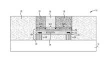
- FIGS. 1A and 1Bprovide an exemplary microelectronics package 10 according to one embodiment of the present disclosure.
- FIG. 1Ashows a cross-sectional view of the exemplary microelectronics package 10
- FIG. 1Bshows a top view of the exemplary microelectronics package 10 .
- the microelectronics package 10includes a module substrate 12 , a thinned flip-chip die 14 , a first magnetically enhanced mold compound component 16 , a first mold compound component 18 , and a second mold compound component 20 .
- the microelectronics package 10may include multiple thinned flip-chip dies.
- the module substrate 12may be formed from a laminate, a wafer level fan out (WLFO) carrier, a lead frame, a ceramic carrier, or the like.
- the thinned flip-chip die 14includes a device layer 22 , a number of interconnects 24 extending from a lower surface of the device layer 22 and coupled to the module substrate 12 , a dielectric layer 26 over an upper surface of the device layer 22 , and essentially no silicon handle layer (not shown) over the dielectric layer 26 .
- essentially no silicon handle layer over the dielectric layer 26refers to at most 2 ⁇ m silicon handle layer over the dielectric layer 26 .
- the thinned flip-chip die 14has an upper surface including a first surface portion SP 1 and a second surface portion SP 2 surrounding the first surface portion SP 1 .
- the upper surface of the thinned flip-chip die 14is an upper surface of the dielectric layer 26 .
- the upper surface of the thinned flip-chip die 14is an upper surface of the thin layer of the silicon handle layer (not shown).
- the device layer 22may be formed of silicon oxide or the like, and the dielectric layer 26 may be formed of silicon oxide or the like, which may serve as an etch stop in a process to remove the silicon handle layer (more details in following discussion).
- an inductor 28 and a number of non-inductive elements 30may be embedded.
- the inductor 28is underlying the first surface portion SP 1 of the thinned flip-chip die 14 and not underlying the second surface portion SP 2 of the thinned flip-chip die 14 .
- the non-inductive elements 30are underlying the second surface portion SP 2 of the thinned flip-chip die 14 .
- the first magnetically enhanced mold compound component 16is formed directly over the first surface portion SP 1 of the thinned flip-chip die 14 , while the first mold compound component 18 is formed directly over the second surface portion SP 2 of the thinned flip-chip die 14 and not over the first surface portion SP 1 of the thinned flip-chip die 14 .
- the first mold compound component 18is surrounding the first magnetically enhanced mold compound component 16 . Consequently, the first magnetically enhanced mold compound component 16 resides over the inductor 28 and the first mold compound component 18 resides over the non-inductive elements 30 .
- the first magnetically enhanced mold compound component 16may significantly increase the inductance value of the inductor 28 and/or improve the quality factor of the inductor 28 .
- an upper surface of the first magnetically enhanced mold compound component 16is coplanar with an upper surface of the first mold compound component 18 .
- the first magnetically enhanced mold compound component 16has a thickness between 1 ⁇ m and 400 ⁇ m.
- the first magnetically enhanced mold compound component 16may be formed from polymer mixed with at least one magnetically enhanced powder, where the at least one magnetically enhanced powder may be a ferro-magnetic material or a ferri-magnetic material.
- One exemplary magnetically enhanced powderis sintered Magnesium-Zinc. Utilizing different magnetically enhanced powders, or with different concentrations of one magnetically enhanced powder, the first magnetically enhanced mold compound component 16 may have 1.1 times to 1000 times improvement in the magnetic permeability.
- the first mold compound component 18may be a high thermal conductivity mold compound component and may be formed from a thermoset or thermoplastic material. Compared to a normal mold compound component having 1 w/m ⁇ k thermal conductivity, a high thermal conductivity mold compound component may have 2.5 w/m ⁇ k ⁇ 50 w/m ⁇ k or greater thermal conductivity, such as Hitachi Chemical Electronic Materials GE-506HT. The higher the thermal conductivity, the better the heat dissipation performance of the microelectronics package 10 .
- the second mold compound component 20resides over the module substrate 12 and encapsulates at least the sides of the first mold compound component 18 and the thinned flip-chip die 14 .
- a portion of the first mold compound component 18may reside over an upper surface of the second mold compound component 20 (not shown).
- the second mold compound component 20may be formed from the same or different material as the first mold compound component 18 .
- the second mold compound component 20does not have a thermal conductivity requirement in higher performing embodiments.
- One exemplary material used to form the second mold compound component 20is an organic epoxy resin system.
- the microelectronics package 10may further include an underfilling layer 32 , as shown in FIG. 2 .
- the underfilling layer 32resides over the upper surface of the module substrate 12 , such that the underfilling layer 32 encapsulates the interconnects 24 and underfills the thinned flip-chip die 14 between the lower surface of the device layer 22 and the upper surface of the module substrate 12 .
- the second mold compound component 20resides over the underfilling layer 32 , and encapsulates at least the sides of the first mold compound component 18 , the sides of the dielectric layer 26 , and the sides of the device layer 22 .
- the underfilling layer 32may be formed from the same or different material as the second mold compound component 20 .
- inductive elementsmay be embedded in the device layer 22 of the thinned flip-chip die 14 .
- a transmission line 28 Tis embedded in the device layer 22 and the first magnetically enhanced mold compound component 16 resides over the transmission line 28 T.
- a coupler 28 Cis embedded in the device layer 22 of the thinned flip-chip die 14 and the first magnetically enhanced mold compound component 16 resides over the coupler 28 C.
- the first magnetically enhanced mold compound component 16may reside over multiple inductors 28 that are embedded in the device layer 22 .
- the first magnetically enhanced mold compound component 16is a contiguous section, which may increase coupling between the adjacent inductors 28 .
- other inductive elementssuch as transmission lines and couplers
- These multiple inductive elements embedded in the device layer 22may be laterally adjacent to each other without overlaps.
- the thinned flip-chip die 14has an upper surface including a first surface portion SP 1 , a second surface portion SP 2 , and a third surface portion SP 3 .
- the second surface portion SP 2is surrounding the first surface portion SP 1 and the third surface portion SP 3 , and the second surface portion SP 2 may separate the first surface portion SP 1 from the third surface portion SP 3 .
- There is a first inductor 28which is embedded in the device layer 22 , underlying the first surface portion SP 1 and not underlying the second surface portion SP 2 .
- a second inductor 28 ′which is embedded in the device layer 22 , underlying the third surface portion SP 3 and not underlying the second surface portion SP 2 .
- the first magnetically enhanced mold compound component 16is formed directly over the first surface portion SP 1 of the thinned flip-chip die 14
- a second magnetically enhanced mold compound component 16 ′is formed directly over the third surface portion SP 3 of the thinned flip-chip die 14
- the first mold compound component 18is formed directly over the second surface portion SP 2 of the thinned flip-chip die 14 and not over the first surface portion SP 1 or the third surface portion SP 3 of the thinned flip-chip die 14 .
- Both the first magnetically enhanced mold compound component 16 and the second magnetically enhanced mold compound component 16 ′are surrounded by the first mold compound component 18 .
- the first magnetically enhanced mold compound component 16may be separated from the second magnetically enhanced mold compound component 16 ′ by the first mold compound component 18 .
- the first magnetically enhanced mold compound component 16 and the second magnetically enhanced mold compound component 16 ′may be formed from an identical material or formed from different materials. By definition, materials are different if they include different elements or have a different element composition. Utilizing different materials or with different concentrations of one magnetically enhanced powder, the first magnetically enhanced mold compound 16 and the second magnetically enhanced mold compound 16 ′ may have different degrees of magnetic enhancement. Further, the first inductor 28 and/or the second inductor 28 ′ may be replaced by other inductive elements (such as transmission lines and couplers).
- FIGS. 7-19provide exemplary steps to fabricate the exemplary microelectronics package 10 shown in FIG. 1A .
- the exemplary stepsare illustrated in a series, the exemplary steps are not necessarily order dependent. Some steps may be done in a different order than that presented. Further, processes within the scope of this disclosure may include fewer or more steps than those illustrated in FIGS. 7-19 .
- a flip-chip die 14 Fis attached to an upper surface of the module substrate 12 as depicted in FIG. 7 .
- the flip-chip die 14 Fincludes the device layer 22 , the interconnects 24 extending from the lower surface of the device layer 22 and coupled to the module substrate 12 , the dielectric layer 26 over the upper surface of the device layer 22 , and a silicon handle layer 34 over the dielectric layer 26 .
- the backside of the silicon handle layer 34will generally be the tallest component after the attaching process.
- the inductor 28 and the non-inductive elements 30may be embedded.
- the device layer 22may have a thickness between 4 ⁇ m and 7 ⁇ m
- the interconnects 24may have a thickness between 15 ⁇ m and 200 ⁇ m
- the dielectric layer 26may have a thickness between 0.2 ⁇ m and 2 ⁇ m
- the silicon handle layer 34may have a thickness between 150 ⁇ m and 500 ⁇ m. It will be clear to those skilled in the art that modifications to these thicknesses may be also considered within the scope of the concepts disclosed herein.
- a second mold compound 20 Mis then applied over the upper surface of the module substrate 12 such that the flip-chip die 14 F is encapsulated by the second mold compound 20 M as illustrated in FIG. 8 .
- the second mold compound 20 Mmay be applied by various procedures, such as sheet molding, overmolding, compression molding, transfer molding, dam fill encapsulation, and screen print encapsulation.
- the second mold compound 20 Mmay be formed from an organic epoxy resin system or the like, such as Hitachi Chemical Electronic Materials GE-100LFC, which can be used as an etchant barrier to protect the flip-chip die 14 F against etching chemistries such as potassium hydroxide (KOH), sodium hydroxide (NaOH), and acetylcholine (ACH).
- KOHpotassium hydroxide
- NaOHsodium hydroxide
- ACHacetylcholine
- a curing process(not shown) is followed to harden the second mold compound 20 M to form the second mold compound component 20 .
- the curing temperaturemay be between
- the final microelectronics package 10includes the underfilling layer 32 , which is formed from a different material to the second mold compound 20 M, there may be extra steps to form the underfilling layer 32 (not shown) before applying the second mold compound 20 M over the upper surface of the module substrate 12 .
- Forming the underfilling layer 32is provided by applying an underfilling material over the upper surface of the module substrate 12 and then curing the underfilling material to form the underfilling layer 32 .
- the underfilling layer 32encapsulates the interconnects 24 and underfills the flip-chip die 14 F between the lower surface of the device layer 22 and the upper surface of the module substrate 12 .
- the second mold compound 20 Mis then applied over the underfilling layer 32 , and encapsulates at least the sides of the silicon handle layer 34 , the sides of the dielectric layer 26 , and the sides of the device layer 22 .
- a curing process(not shown) is followed to harden the second mold compound 20 M to form the second mold compound component 20 .
- the second mold compound component 20is thinned down to expose the backside of the silicon handle layer 34 of the flip-chip die 14 F, as shown in FIG. 9 .
- the thinning proceduremay be done with a mechanical grinding process.
- the following stepis to remove substantially the entire silicon handle layer 34 of the flip-chip die 14 F to provide the thinned flip-chip die 14 that has the upper surface at a bottom of a first cavity 36 , as shown in FIG. 10 .
- removing substantially the entire silicon handle layer 34refers to removal of at least 95% of the entire silicon handle layer 34 , and perhaps a portion of the dielectric layer 26 .
- the thinned flip-chip die 14may refer to a device including a device layer 22 , a dielectric layer 26 over the upper surface of the device layer 22 , and the interconnects 24 extending from the lower surface of the device layer 22 and coupled to the module substrate 12 , where the upper surface of the dielectric layer 26 is the upper surface of the thinned flip-chip die 14 .
- the thinned flip-chip die 14may refer to a device including a device layer 22 , a dielectric layer 26 over an upper surface of the device layer 22 , a thin layer (less than 1 ⁇ m) of the silicon handle layer 34 left over the dielectric layer 26 , and a number of interconnects 24 extending from the lower surface of the device layer 22 and coupled to the module substrate 12 , where the upper surface of the thin layer of the silicon handle layer 34 is the upper surface of the thinned flip-chip die 14 .
- Removing substantially the entire silicon handle layer 34may be provided by an etching process with a wet/dry etchant chemistry, which may be KOH, ACH, NaOH or the like.
- the upper surface of the thinned flip-chip die 14includes the first surface portion SP 1 and the second surface portion SP 2 surrounding the first surface portion SP 1 .
- the inductor 28 embedded in the device layer 22is underlying the first surface portion SP 1 and not underlying the second surface portion SP 2 .
- the non-inductive elements 30 embedded in the device layer 22are underlying the second surface portion SP 2 of the thinned flip-chip die 14 .
- a process for providing a first mold compound component 18 over the second surface portion SP 2 of the thinned flip-chip die 14is illustrated according to one embodiment of the present disclosure.
- a molding block 38is placed within the first cavity 36 and over the first surface portion SP 1 of the thinned flip-chip die 14 , as illustrated in FIG. 11 .
- only the first surface portion SP 1 of the thinned flip-chip die 14is blocked by the molding block 38 , while the second surface portion SP 2 of the thinned flip-chip die 14 is exposed to the first cavity 36 .
- the molding block 38may be formed from a suitable patternable sacrificial material, such as polyimide, with a height between 2 ⁇ m and 300 ⁇ m. Normally, the height of the molding block 34 is no less than a depth of the first cavity 36 .
- a first mold compound 18 Mis applied to substantially fill the first cavity 36 , and directly contacts the second surface portion SP 2 of the thinned flip-chip die 14 , as illustrated in FIG. 12 .
- the first mold compound 18 Mmay encapsulate the molding block 38 and reside over an upper surface of the second mold compound component 20 , but does not directly reside over the first surface portion SP 1 of the thinned flip-chip die 14 .
- the first mold compound 18 Mmay be applied by various procedures, such as sheet molding, overmolding, compression molding, transfer molding, dam fill encapsulation, and screen print encapsulation.
- a curing process(not shown) is followed to harden the first mold compound 18 M in order to form the first mold compound component 18 .
- the curing temperatureis between 125° C. and 300° C. depending on which material is used as the first mold compound 18 M.
- the first mold compound component 18is then thinned to expose an upper surface of the molding block 38 , as illustrated in FIG. 13 .
- the thinning proceduremay be done with a mechanical grinding process.
- the molding block 38is removed to form a second cavity 40 and expose the first surface portion SP 1 of the thinned flip-chip die 14 at a bottom of the second cavity 40 , as illustrated in FIG. 14 .
- the removal of the molding block 38may be provided by a dry or wet selective etching process. If the molding block 38 is formed from polyimide, a hot NaOH or KOH solution may be used in selectively removing the molding block 38 .
- FIGS. 15-17an alternate process for providing the first mold compound component 18 over the second surface portion SP 2 of the thinned flip-chip die 14 is illustrated in FIGS. 15-17 .
- the first mold compound 18 Mis applied to substantially fill the first cavity 36 , and directly contacts the upper surface of the thinned flip-chip die 14 , as illustrated in FIG. 15 .
- the first mold compound 18 Mmay further reside over an upper surface of the second mold compound component 20 .
- the first mold compound 18 Mmay be applied by various procedures, such as sheet molding, overmolding, compression molding, transfer molding, dam fill encapsulation, and screen print encapsulation.
- a curing process(not shown) is followed to harden the first mold compound 18 M to form the first mold compound component 18 .
- the curing temperatureis between 125° C. and 300° C. depending on which material is used as the first mold compound 18 M.
- the upper surface of the first mold compound component 18is then planarized, as illustrated in FIG. 16 .
- a mechanical grinding processmay be used for planarization.
- a portion of the first mold compound component 18is removed to form the second cavity 40 , as illustrated in FIG. 17 .
- the first surface portion SP 1 of the thinned flip-chip die 14is exposed at the bottom of the second cavity 40 and the second surface portion SP 2 of the thinned flip-chip die 14 is not exposed to the second cavity 40 .
- the removal of the portion of the first mold compound component 18 to expose the first surface portion SP 1may be provided by a laser ablation system.
- a process for providing a first magnetically enhanced mold compound component 16 over the first surface portion SP 1 of the thinned flip-chip die 14is illustrated according to one embodiment of the present disclosure.
- the first magnetically enhanced mold compound 16 Mis applied to substantially fill the second cavity 40 and directly contact the first surface portion SP 1 .
- a portion of the first magnetically enhanced mold compound 16 Mmay reside over an upper surface of the first mold compound component 18 .
- the first magnetically enhanced mold compound 16 Mmay be applied by various procedures, such as sheet molding, overmolding, compression molding, transfer molding, dam fill encapsulation, and screen print encapsulation.
- a curing process(not shown) is followed to harden the first magnetically enhanced mold compound 16 M to form the first magnetically enhanced mold compound component 16 .
- the curing temperatureis between 125° C. and 300° C. depending on which material is used as the first magnetically enhanced mold compound 16 M.
- the upper surface of the first magnetically enhanced mold compound component 16is planarized, such that the upper surface of the first magnetically enhanced mold compound component 16 and the upper surface of the first mold compound component 18 may be coplanar, as illustrated in FIG. 19 .
- a mechanical grinding processmay be used for planarization.
- the first magnetically enhanced mold compound component 16is surrounded by the first mold compound component 18 .
Landscapes
- Engineering & Computer Science (AREA)
- Microelectronics & Electronic Packaging (AREA)
- Computer Hardware Design (AREA)
- Power Engineering (AREA)
- Physics & Mathematics (AREA)
- Condensed Matter Physics & Semiconductors (AREA)
- General Physics & Mathematics (AREA)
- Manufacturing & Machinery (AREA)
- Structures Or Materials For Encapsulating Or Coating Semiconductor Devices Or Solid State Devices (AREA)
Abstract
Description
This application claims the benefit of provisional patent application Ser. No. 62/333,317, filed May 9, 2016. This application is related to concurrently filed U.S. patent application Ser. No. 15/287,273, entitled “MICROELECTRONICS PACKAGE WITH INDUCTIVE ELEMENT AND MAGNETICALLY ENHANCED MOLD COMPOUND COMPONENT” the disclosures of which are hereby incorporated herein by reference in their entirety.
The present disclosure relates to a microelectronics package and a process for making the same, and more particularly to a microelectronics package with an inductive element and a magnetically enhanced mold compound component, and a process to form the magnetically enhanced mold compound component over the inductive element.
Silicon on insulator (SOI) substrates are widely used in forming semiconductor dies due to the low cost of silicon materials, large scale capacity of wafer production, well-established semiconductor design tools, and well-established semiconductor manufacturing techniques. However, harmonic generations and low resistivity values of the SOI substrates severely limit the SOI's usage in radio-frequency (RF) applications. By using SOI substrates in RF fabrications, an interface between the silicon handle layer and an adjacent dielectric layer will generate unwanted harmonic and intermodulation products. Such spectrum degradation causes a number of significant system issues such as unwanted generation of signals in other RF bands that the system is attempting to avoid. In addition, the relatively low resistivity encountered in the silicon handle layer limits the performance and quality factor of inductive elements embedded in the semiconductor dies, such as inductors, transmission lines and couples, by the generation of unwanted RF current loss in the silicon handle layer.
Further, with the current popularity of portable communication devices, high speed and high performance transistors are more densely integrated on semiconductor dies. The amount of heat generated by the semiconductor dies will increase significantly due to the large number of transistors integrated on the semiconductor dies, the large amount of power passing through the transistors, and the high operation speed of the transistors.
Accordingly, there remains a need for improved microelectronics package designs that improve the quality factor and inductance value of the inductive elements, and accommodate the increased heat generation of the semiconductor dies. In addition, there is also a need to enhance the performance of the microelectronics package without increasing the package size.
The present disclosure relates to a microelectronics package with an inductive element and a magnetically enhanced mold compound component, and a process for making the same. The disclosed microelectronics package includes a module substrate, a thinned flip-chip die with an upper surface that includes a first surface portion and a second surface portion surrounding the first surface portion, the magnetically enhanced mold compound component, and a mold compound component. The thinned flip-chip die includes a device layer with the inductive element embedded therein, a number of interconnects extending from a lower surface of the device layer and coupled to the module substrate, and a dielectric layer over an upper surface of the device layer. Herein, the inductive element is underlying the first surface portion and not underlying the second surface portion. The magnetically enhanced mold compound component is formed over the first surface portion. The mold compound component is formed over the second surface portion, not over the first surface portion, and surrounding the magnetically enhanced mold compound component.
According to an exemplary process, a precursor package including a module substrate and a thinned flip-chip die is provided. The thinned flip-chip die has an upper surface that includes a first surface portion and a second surface portion surrounding the first surface portion. The thinned flip-chip die is attached to the module substrate and includes a device layer with an inductive element that is embedded in the device layer. Herein, the inductive element is underlying the first surface portion and not underlying the second surface portion. Next, a mold compound component is provided over the second surface portion such that the mold compound component does not cover the first surface portion. Finally, a magnetically enhanced mold compound component is provided over the first surface portion to form a microelectronics package. The magnetically enhanced mold compound component is surrounded by the mold compound component.
Those skilled in the art will appreciate the scope of the present disclosure and realize additional aspects thereof after reading the following detailed description of the preferred embodiments in association with the accompanying drawing figures.
The accompanying drawing figures incorporated in and forming a part of this specification illustrate several aspects of the disclosure, and together with the description serve to explain the principles of the disclosure.
It will be understood that for clear illustrations,FIGS. 1A-19 may not be drawn to scale.
The embodiments set forth below represent the necessary information to enable those skilled in the art to practice the embodiments and illustrate the best mode of practicing the embodiments. Upon reading the following description in light of the accompanying drawing figures, those skilled in the art will understand the concepts of the disclosure and will recognize applications of these concepts not particularly addressed herein. It should be understood that these concepts and applications fall within the scope of the disclosure and the accompanying claims.
It will be understood that, although the terms first, second, etc. may be used herein to describe various elements, these elements should not be limited by these terms. These terms are only used to distinguish one element from another. For example, a first element could be termed a second element, and, similarly, a second element could be termed a first element, without departing from the scope of the present disclosure. As used herein, the term “and/or” includes any and all combinations of one or more of the associated listed items.
It will be understood that when an element such as a layer, region, or substrate is referred to as being “on” or extending “onto” another element, it can be directly on or extend directly onto the other element or intervening elements may also be present. In contrast, when an element is referred to as being “directly on” or extending “directly onto” another element, there are no intervening elements present. Likewise, it will be understood that when an element such as a layer, region, or substrate is referred to as being “over” or extending “over” another element, it can be directly over or extend directly over the other element or intervening elements may also be present. In contrast, when an element is referred to as being “directly over” or extending “directly over” another element, there are no intervening elements present. It will also be understood that when an element is referred to as being “connected” or “coupled” to another element, it can be directly connected or coupled to the other element or intervening elements may be present. In contrast, when an element is referred to as being “directly connected” or “directly coupled” to another element, there are no intervening elements present.
Relative terms such as “below” or “above” or “upper” or “lower” or “horizontal” or “vertical” may be used herein to describe a relationship of one element, layer, or region to another element, layer, or region as illustrated in the Figures. It will be understood that these terms and those discussed above are intended to encompass different orientations of the device in addition to the orientation depicted in the Figures.
The terminology used herein is for the purpose of describing particular embodiments only and is not intended to be limiting of the disclosure. As used herein, the singular forms “a,” “an,” and “the” are intended to include the plural forms as well, unless the context clearly indicates otherwise. It will be further understood that the terms “comprises,” “comprising,” “includes,” and/or “including” when used herein specify the presence of stated features, integers, steps, operations, elements, and/or components, but do not preclude the presence or addition of one or more other features, integers, steps, operations, elements, components, and/or groups thereof.
Unless otherwise defined, all terms (including technical and scientific terms) used herein have the same meaning as commonly understood by one of ordinary skill in the art to which this disclosure belongs. It will be further understood that terms used herein should be interpreted as having a meaning that is consistent with their meaning in the context of this specification and the relevant art and will not be interpreted in an idealized or overly formal sense unless expressly so defined herein.
The present disclosure relates to a microelectronics package having an inductive element and a magnetically enhanced mold compound component, and a process for making the same.FIGS. 1A and 1B provide anexemplary microelectronics package 10 according to one embodiment of the present disclosure.FIG. 1A shows a cross-sectional view of theexemplary microelectronics package 10, andFIG. 1B shows a top view of theexemplary microelectronics package 10. For the purpose of this illustration, themicroelectronics package 10 includes amodule substrate 12, a thinned flip-chip die14, a first magnetically enhancedmold compound component 16, a firstmold compound component 18, and a secondmold compound component 20. In different applications, themicroelectronics package 10 may include multiple thinned flip-chip dies.
In detail, themodule substrate 12 may be formed from a laminate, a wafer level fan out (WLFO) carrier, a lead frame, a ceramic carrier, or the like. The thinned flip-chip die14 includes adevice layer 22, a number ofinterconnects 24 extending from a lower surface of thedevice layer 22 and coupled to themodule substrate 12, adielectric layer 26 over an upper surface of thedevice layer 22, and essentially no silicon handle layer (not shown) over thedielectric layer 26. Herein, essentially no silicon handle layer over thedielectric layer 26 refers to at most 2 μm silicon handle layer over thedielectric layer 26. The thinned flip-chip die14 has an upper surface including a first surface portion SP1 and a second surface portion SP2 surrounding the first surface portion SP1. In some applications, the upper surface of the thinned flip-chip die14 is an upper surface of thedielectric layer 26. For other cases, the upper surface of the thinned flip-chip die14 is an upper surface of the thin layer of the silicon handle layer (not shown). Thedevice layer 22 may be formed of silicon oxide or the like, and thedielectric layer 26 may be formed of silicon oxide or the like, which may serve as an etch stop in a process to remove the silicon handle layer (more details in following discussion). Within thedevice layer 22, aninductor 28 and a number of non-inductive elements30 (such as diodes, transistors, mechanical switches, and resonators) may be embedded. Theinductor 28 is underlying the first surface portion SP1 of the thinned flip-chip die14 and not underlying the second surface portion SP2 of the thinned flip-chip die14. Thenon-inductive elements 30 are underlying the second surface portion SP2 of the thinned flip-chip die14.
The first magnetically enhancedmold compound component 16 is formed directly over the first surface portion SP1 of the thinned flip-chip die14, while the firstmold compound component 18 is formed directly over the second surface portion SP2 of the thinned flip-chip die14 and not over the first surface portion SP1 of the thinned flip-chip die14. The firstmold compound component 18 is surrounding the first magnetically enhancedmold compound component 16. Consequently, the first magnetically enhancedmold compound component 16 resides over theinductor 28 and the firstmold compound component 18 resides over thenon-inductive elements 30. Because the first magnetically enhancedmold compound component 16 is adjacent to theinductor 28 and has a magnetically enhanced feature, the first magnetically enhancedmold compound component 16 may significantly increase the inductance value of theinductor 28 and/or improve the quality factor of theinductor 28. Normally, an upper surface of the first magnetically enhancedmold compound component 16 is coplanar with an upper surface of the firstmold compound component 18. The first magnetically enhancedmold compound component 16 has a thickness between 1 μm and 400 μm.
The first magnetically enhancedmold compound component 16 may be formed from polymer mixed with at least one magnetically enhanced powder, where the at least one magnetically enhanced powder may be a ferro-magnetic material or a ferri-magnetic material. One exemplary magnetically enhanced powder is sintered Magnesium-Zinc. Utilizing different magnetically enhanced powders, or with different concentrations of one magnetically enhanced powder, the first magnetically enhancedmold compound component 16 may have 1.1 times to 1000 times improvement in the magnetic permeability.
The firstmold compound component 18 may be a high thermal conductivity mold compound component and may be formed from a thermoset or thermoplastic material. Compared to a normal mold compound component having 1 w/m·k thermal conductivity, a high thermal conductivity mold compound component may have 2.5 w/m·k˜50 w/m·k or greater thermal conductivity, such as Hitachi Chemical Electronic Materials GE-506HT. The higher the thermal conductivity, the better the heat dissipation performance of themicroelectronics package 10.
In addition, the secondmold compound component 20 resides over themodule substrate 12 and encapsulates at least the sides of the firstmold compound component 18 and the thinned flip-chip die14. In some applications, a portion of the firstmold compound component 18 may reside over an upper surface of the second mold compound component20 (not shown). Herein, the secondmold compound component 20 may be formed from the same or different material as the firstmold compound component 18. However, unlike the firstmold compound component 18, the secondmold compound component 20 does not have a thermal conductivity requirement in higher performing embodiments. One exemplary material used to form the secondmold compound component 20 is an organic epoxy resin system.
In some applications, themicroelectronics package 10 may further include anunderfilling layer 32, as shown inFIG. 2 . Theunderfilling layer 32 resides over the upper surface of themodule substrate 12, such that theunderfilling layer 32 encapsulates theinterconnects 24 and underfills the thinned flip-chip die14 between the lower surface of thedevice layer 22 and the upper surface of themodule substrate 12. Herein, the secondmold compound component 20 resides over theunderfilling layer 32, and encapsulates at least the sides of the firstmold compound component 18, the sides of thedielectric layer 26, and the sides of thedevice layer 22. Theunderfilling layer 32 may be formed from the same or different material as the secondmold compound component 20.
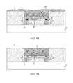
It will be clear to those skilled in the art that other inductive elements may be embedded in thedevice layer 22 of the thinned flip-chip die14. As shown inFIGS. 3A-3B , atransmission line 28T is embedded in thedevice layer 22 and the first magnetically enhancedmold compound component 16 resides over thetransmission line 28T. Further, as shown inFIGS. 4A-4B , a coupler28C is embedded in thedevice layer 22 of the thinned flip-chip die14 and the first magnetically enhancedmold compound component 16 resides over the coupler28C.
In another embodiment, as shown inFIGS. 5A-5B , the first magnetically enhancedmold compound component 16 may reside overmultiple inductors 28 that are embedded in thedevice layer 22. Herein, the first magnetically enhancedmold compound component 16 is a contiguous section, which may increase coupling between theadjacent inductors 28. In different applications, other inductive elements (such as transmission lines and couplers) may also reside under the same contiguous section of the first magnetically enhancedmold compound component 16. These multiple inductive elements embedded in thedevice layer 22 may be laterally adjacent to each other without overlaps.
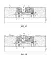
In another embodiment, as shown inFIGS. 6A-6B , the thinned flip-chip die14 has an upper surface including a first surface portion SP1, a second surface portion SP2, and a third surface portion SP3. The second surface portion SP2 is surrounding the first surface portion SP1 and the third surface portion SP3, and the second surface portion SP2 may separate the first surface portion SP1 from the third surface portion SP3. There is afirst inductor 28, which is embedded in thedevice layer 22, underlying the first surface portion SP1 and not underlying the second surface portion SP2. Also, there is asecond inductor 28′, which is embedded in thedevice layer 22, underlying the third surface portion SP3 and not underlying the second surface portion SP2. The first magnetically enhancedmold compound component 16 is formed directly over the first surface portion SP1 of the thinned flip-chip die14, while a second magnetically enhancedmold compound component 16′ is formed directly over the third surface portion SP3 of the thinned flip-chip die14. The firstmold compound component 18 is formed directly over the second surface portion SP2 of the thinned flip-chip die14 and not over the first surface portion SP1 or the third surface portion SP3 of the thinned flip-chip die14. Both the first magnetically enhancedmold compound component 16 and the second magnetically enhancedmold compound component 16′ are surrounded by the firstmold compound component 18. The first magnetically enhancedmold compound component 16 may be separated from the second magnetically enhancedmold compound component 16′ by the firstmold compound component 18. In different applications, the first magnetically enhancedmold compound component 16 and the second magnetically enhancedmold compound component 16′ may be formed from an identical material or formed from different materials. By definition, materials are different if they include different elements or have a different element composition. Utilizing different materials or with different concentrations of one magnetically enhanced powder, the first magnetically enhancedmold compound 16 and the second magnetically enhancedmold compound 16′ may have different degrees of magnetic enhancement. Further, thefirst inductor 28 and/or thesecond inductor 28′ may be replaced by other inductive elements (such as transmission lines and couplers).
Initially, a flip-chip die 14F is attached to an upper surface of themodule substrate 12 as depicted inFIG. 7 . For the purpose of this illustration, the flip-chip die14F includes thedevice layer 22, theinterconnects 24 extending from the lower surface of thedevice layer 22 and coupled to themodule substrate 12, thedielectric layer 26 over the upper surface of thedevice layer 22, and asilicon handle layer 34 over thedielectric layer 26. As such, the backside of thesilicon handle layer 34 will generally be the tallest component after the attaching process. Within thedevice layer 22, theinductor 28 and the non-inductive elements30 (such as diodes, transistors, mechanical switches, and resonators) may be embedded. Thedevice layer 22 may have a thickness between 4 μm and 7 μm, theinterconnects 24 may have a thickness between 15 μm and 200 μm, thedielectric layer 26 may have a thickness between 0.2 μm and 2 μm, and thesilicon handle layer 34 may have a thickness between 150 μm and 500 μm. It will be clear to those skilled in the art that modifications to these thicknesses may be also considered within the scope of the concepts disclosed herein.
Asecond mold compound 20M is then applied over the upper surface of themodule substrate 12 such that the flip-chip die 14F is encapsulated by thesecond mold compound 20M as illustrated inFIG. 8 . Thesecond mold compound 20M may be applied by various procedures, such as sheet molding, overmolding, compression molding, transfer molding, dam fill encapsulation, and screen print encapsulation. Thesecond mold compound 20M may be formed from an organic epoxy resin system or the like, such as Hitachi Chemical Electronic Materials GE-100LFC, which can be used as an etchant barrier to protect the flip-chip die 14F against etching chemistries such as potassium hydroxide (KOH), sodium hydroxide (NaOH), and acetylcholine (ACH). A curing process (not shown) is followed to harden thesecond mold compound 20M to form the secondmold compound component 20. The curing temperature may be between 125° C. and 300° C. depending on which material is used as thesecond mold compound 20M.
Notice that, if thefinal microelectronics package 10 includes theunderfilling layer 32, which is formed from a different material to thesecond mold compound 20M, there may be extra steps to form the underfilling layer32 (not shown) before applying thesecond mold compound 20M over the upper surface of themodule substrate 12. Forming theunderfilling layer 32 is provided by applying an underfilling material over the upper surface of themodule substrate 12 and then curing the underfilling material to form theunderfilling layer 32. Theunderfilling layer 32 encapsulates theinterconnects 24 and underfills the flip-chip die 14F between the lower surface of thedevice layer 22 and the upper surface of themodule substrate 12. Thesecond mold compound 20M is then applied over theunderfilling layer 32, and encapsulates at least the sides of thesilicon handle layer 34, the sides of thedielectric layer 26, and the sides of thedevice layer 22. A curing process (not shown) is followed to harden thesecond mold compound 20M to form the secondmold compound component 20.
Next, the secondmold compound component 20 is thinned down to expose the backside of thesilicon handle layer 34 of the flip-chip die 14F, as shown inFIG. 9 . The thinning procedure may be done with a mechanical grinding process. The following step is to remove substantially the entiresilicon handle layer 34 of the flip-chip die14F to provide the thinned flip-chip die14 that has the upper surface at a bottom of afirst cavity 36, as shown inFIG. 10 . Herein, removing substantially the entiresilicon handle layer 34 refers to removal of at least 95% of the entiresilicon handle layer 34, and perhaps a portion of thedielectric layer 26. As such, in some applications, the thinned flip-chip die14 may refer to a device including adevice layer 22, adielectric layer 26 over the upper surface of thedevice layer 22, and theinterconnects 24 extending from the lower surface of thedevice layer 22 and coupled to themodule substrate 12, where the upper surface of thedielectric layer 26 is the upper surface of the thinned flip-chip die14. For other cases, the thinned flip-chip die14 may refer to a device including adevice layer 22, adielectric layer 26 over an upper surface of thedevice layer 22, a thin layer (less than 1 μm) of thesilicon handle layer 34 left over thedielectric layer 26, and a number ofinterconnects 24 extending from the lower surface of thedevice layer 22 and coupled to themodule substrate 12, where the upper surface of the thin layer of thesilicon handle layer 34 is the upper surface of the thinned flip-chip die14. Removing substantially the entiresilicon handle layer 34 may be provided by an etching process with a wet/dry etchant chemistry, which may be KOH, ACH, NaOH or the like.
Further, the upper surface of the thinned flip-chip die14 includes the first surface portion SP1 and the second surface portion SP2 surrounding the first surface portion SP1. Theinductor 28 embedded in thedevice layer 22 is underlying the first surface portion SP1 and not underlying the second surface portion SP2. Thenon-inductive elements 30 embedded in thedevice layer 22 are underlying the second surface portion SP2 of the thinned flip-chip die14.
With reference toFIGS. 11 through 14 , a process for providing a firstmold compound component 18 over the second surface portion SP2 of the thinned flip-chip die14 is illustrated according to one embodiment of the present disclosure. After the removing step is done, amolding block 38 is placed within thefirst cavity 36 and over the first surface portion SP1 of the thinned flip-chip die14, as illustrated inFIG. 11 . Herein, only the first surface portion SP1 of the thinned flip-chip die14 is blocked by themolding block 38, while the second surface portion SP2 of the thinned flip-chip die14 is exposed to thefirst cavity 36. Themolding block 38 may be formed from a suitable patternable sacrificial material, such as polyimide, with a height between 2 μm and 300 μm. Normally, the height of themolding block 34 is no less than a depth of thefirst cavity 36.
Next, afirst mold compound 18M is applied to substantially fill thefirst cavity 36, and directly contacts the second surface portion SP2 of the thinned flip-chip die14, as illustrated inFIG. 12 . Thefirst mold compound 18M may encapsulate themolding block 38 and reside over an upper surface of the secondmold compound component 20, but does not directly reside over the first surface portion SP1 of the thinned flip-chip die14. Thefirst mold compound 18M may be applied by various procedures, such as sheet molding, overmolding, compression molding, transfer molding, dam fill encapsulation, and screen print encapsulation. A curing process (not shown) is followed to harden thefirst mold compound 18M in order to form the firstmold compound component 18. The curing temperature is between 125° C. and 300° C. depending on which material is used as thefirst mold compound 18M.
The firstmold compound component 18 is then thinned to expose an upper surface of themolding block 38, as illustrated inFIG. 13 . The thinning procedure may be done with a mechanical grinding process. Next, themolding block 38 is removed to form asecond cavity 40 and expose the first surface portion SP1 of the thinned flip-chip die14 at a bottom of thesecond cavity 40, as illustrated inFIG. 14 . The removal of themolding block 38 may be provided by a dry or wet selective etching process. If themolding block 38 is formed from polyimide, a hot NaOH or KOH solution may be used in selectively removing themolding block 38.
In another embodiment, an alternate process for providing the firstmold compound component 18 over the second surface portion SP2 of the thinned flip-chip die14 is illustrated inFIGS. 15-17 . After the removal step is done, thefirst mold compound 18M is applied to substantially fill thefirst cavity 36, and directly contacts the upper surface of the thinned flip-chip die14, as illustrated inFIG. 15 . Thefirst mold compound 18M may further reside over an upper surface of the secondmold compound component 20. Thefirst mold compound 18M may be applied by various procedures, such as sheet molding, overmolding, compression molding, transfer molding, dam fill encapsulation, and screen print encapsulation. A curing process (not shown) is followed to harden thefirst mold compound 18M to form the firstmold compound component 18. The curing temperature is between 125° C. and 300° C. depending on which material is used as thefirst mold compound 18M.
The upper surface of the firstmold compound component 18 is then planarized, as illustrated inFIG. 16 . A mechanical grinding process may be used for planarization. Next, a portion of the firstmold compound component 18 is removed to form thesecond cavity 40, as illustrated inFIG. 17 . Herein, the first surface portion SP1 of the thinned flip-chip die14 is exposed at the bottom of thesecond cavity 40 and the second surface portion SP2 of the thinned flip-chip die14 is not exposed to thesecond cavity 40. The removal of the portion of the firstmold compound component 18 to expose the first surface portion SP1 may be provided by a laser ablation system.
With reference toFIGS. 18 through 19 , a process for providing a first magnetically enhancedmold compound component 16 over the first surface portion SP1 of the thinned flip-chip die14 is illustrated according to one embodiment of the present disclosure. As shown inFIG. 18 , the first magnetically enhancedmold compound 16M is applied to substantially fill thesecond cavity 40 and directly contact the first surface portion SP1. A portion of the first magnetically enhancedmold compound 16M may reside over an upper surface of the firstmold compound component 18. The first magnetically enhancedmold compound 16M may be applied by various procedures, such as sheet molding, overmolding, compression molding, transfer molding, dam fill encapsulation, and screen print encapsulation. A curing process (not shown) is followed to harden the first magnetically enhancedmold compound 16M to form the first magnetically enhancedmold compound component 16. The curing temperature is between 125° C. and 300° C. depending on which material is used as the first magnetically enhancedmold compound 16M.
Finally, the upper surface of the first magnetically enhancedmold compound component 16 is planarized, such that the upper surface of the first magnetically enhancedmold compound component 16 and the upper surface of the firstmold compound component 18 may be coplanar, as illustrated inFIG. 19 . A mechanical grinding process may be used for planarization. Herein, the first magnetically enhancedmold compound component 16 is surrounded by the firstmold compound component 18.
Those skilled in the art will recognize improvements and modifications to the preferred embodiments of the present disclosure. All such improvements and modifications are considered within the scope of the concepts disclosed herein and the claims that follow.
Claims (22)
1. An apparatus comprising:
a module substrate;
a thinned flip-chip die, which has an upper surface including a first surface portion and a second surface portion surrounding the first surface portion, comprising:
a device layer including a first inductive element embedded therein, wherein the first inductive element is underlying the first surface portion and is not underlying the second surface portion;
a dielectric layer over an upper surface of the device layer; and
a plurality of interconnects extending from a lower surface of the device layer and coupled to the module substrate;
a first magnetically enhanced mold compound component formed over the first surface portion; and
a first mold compound component formed over the second surface portion and not over the first surface portion, wherein the first mold compound component is surrounding the first magnetically enhanced mold compound component.
2. The apparatus ofclaim 1 wherein:
the upper surface of the thinned flip-chip die further includes a third surface portion surrounded by the second surface portion;
the device layer further comprises a second inductive element embedded therein, wherein the second inductive element is underlying the third surface portion and not underlying the second surface portion; and
a second magnetically enhanced mold compound component is formed over the third surface portion and surrounded by the first mold compound component.
3. The apparatus ofclaim 2 wherein the first magnetically enhanced mold compound component and the second magnetically enhanced mold compound component are formed of an identical material.
4. The apparatus ofclaim 2 wherein the first magnetically enhanced mold compound component and the second magnetically enhanced mold compound component are formed from different materials.
5. The apparatus ofclaim 1 wherein the device layer further comprises a second inductive element that is underlying the first surface portion such that the first magnetically enhanced mold compound component resides over both the first inductive element and the second inductive element.
6. The apparatus ofclaim 1 wherein the device layer further comprises a second inductive element that is underlying the first surface portion and laterally adjacent to the first inductive element such that the first magnetically enhanced mold compound component resides over both the first inductive element and the second inductive element.
7. The apparatus ofclaim 1 wherein the upper surface of the thinned flip-chip die is an upper surface of the dielectric layer.
8. The apparatus ofclaim 1 wherein the first magnetically enhanced mold compound component is formed from polymer mixed with at least one magnetically enhanced powder.
9. The apparatus ofclaim 8 wherein the at least one magnetically enhanced powder is a ferro-magnetic material or a ferri-magnetic material.
10. The apparatus ofclaim 8 wherein the at least one magnetically enhanced powder is sintered Magnesium-Zinc.
11. The apparatus ofclaim 1 wherein the first mold compound component has a thermal conductivity between 2.5w/m·k and 50w/m·k.
12. The apparatus ofclaim 1 further comprising a second mold compound component that resides between the module substrate and the lower surface of the device layer and encapsulates at least sides of the first mold compound component and the thinned flip-chip die.
13. The apparatus ofclaim 12 wherein the first mold compound component and the second mold compound component are formed from a same material.
14. The apparatus ofclaim 12 wherein the first mold compound component and the second mold compound component are formed from different materials.
15. The apparatus ofclaim 12 wherein the second mold compound component is formed from an organic epoxy resin system.
16. The apparatus ofclaim 12 wherein a portion of the first mold compound component further resides over an upper surface of the second mold compound component.
17. The apparatus ofclaim 1 wherein the dielectric layer is formed of silicon oxide.
18. The apparatus ofclaim 1 wherein the first inductive element is one of a group consisting of inductor, transmission line, and coupler.
19. The apparatus ofclaim 1 wherein the device layer further includes at least one of a group consisting of diodes, transistors, mechanical switches, and resonators.
20. The apparatus ofclaim 1 wherein an upper surface of the first magnetically enhanced mold compound component is coplanar with an upper surface of the first mold compound component.
21. The apparatus ofclaim 1 wherein a thickness of the first magnetically enhanced mold compound component is between 1 μm and 400 μm.
22. The apparatus ofclaim 1 wherein the module substrate is one of a group consisting of a laminate, a wafer level fan out (WLFO) carrier, a lead frame, and a ceramic carrier.
Priority Applications (1)
| Application Number | Priority Date | Filing Date | Title |
|---|---|---|---|
| US15/287,202US10090262B2 (en) | 2016-05-09 | 2016-10-06 | Microelectronics package with inductive element and magnetically enhanced mold compound component |
Applications Claiming Priority (2)
| Application Number | Priority Date | Filing Date | Title |
|---|---|---|---|
| US201662333317P | 2016-05-09 | 2016-05-09 | |
| US15/287,202US10090262B2 (en) | 2016-05-09 | 2016-10-06 | Microelectronics package with inductive element and magnetically enhanced mold compound component |
Publications (2)
| Publication Number | Publication Date |
|---|---|
| US20170323860A1 US20170323860A1 (en) | 2017-11-09 |
| US10090262B2true US10090262B2 (en) | 2018-10-02 |
Family
ID=60244013
Family Applications (2)
| Application Number | Title | Priority Date | Filing Date |
|---|---|---|---|
| US15/287,273Active2036-11-01US10062583B2 (en) | 2016-05-09 | 2016-10-06 | Microelectronics package with inductive element and magnetically enhanced mold compound component |
| US15/287,202Active2036-11-03US10090262B2 (en) | 2016-05-09 | 2016-10-06 | Microelectronics package with inductive element and magnetically enhanced mold compound component |
Family Applications Before (1)
| Application Number | Title | Priority Date | Filing Date |
|---|---|---|---|
| US15/287,273Active2036-11-01US10062583B2 (en) | 2016-05-09 | 2016-10-06 | Microelectronics package with inductive element and magnetically enhanced mold compound component |
Country Status (1)
| Country | Link |
|---|---|
| US (2) | US10062583B2 (en) |
Families Citing this family (42)
| Publication number | Priority date | Publication date | Assignee | Title |
|---|---|---|---|---|
| US10085352B2 (en) | 2014-10-01 | 2018-09-25 | Qorvo Us, Inc. | Method for manufacturing an integrated circuit package |
| US9530709B2 (en) | 2014-11-03 | 2016-12-27 | Qorvo Us, Inc. | Methods of manufacturing a printed circuit module having a semiconductor device with a protective layer in place of a low-resistivity handle layer |
| US10773952B2 (en) | 2016-05-20 | 2020-09-15 | Qorvo Us, Inc. | Wafer-level package with enhanced performance |
| US10784149B2 (en) | 2016-05-20 | 2020-09-22 | Qorvo Us, Inc. | Air-cavity module with enhanced device isolation |
| US10103080B2 (en) | 2016-06-10 | 2018-10-16 | Qorvo Us, Inc. | Thermally enhanced semiconductor package with thermal additive and process for making the same |
| US10186499B2 (en)* | 2016-06-30 | 2019-01-22 | Intel IP Corporation | Integrated circuit package assemblies including a chip recess |
| US10486965B2 (en) | 2016-08-12 | 2019-11-26 | Qorvo Us, Inc. | Wafer-level package with enhanced performance |
| US10109550B2 (en) | 2016-08-12 | 2018-10-23 | Qorvo Us, Inc. | Wafer-level package with enhanced performance |
| SG11201901193UA (en) | 2016-08-12 | 2019-03-28 | Qorvo Us Inc | Wafer-level package with enhanced performance |
| US10109502B2 (en) | 2016-09-12 | 2018-10-23 | Qorvo Us, Inc. | Semiconductor package with reduced parasitic coupling effects and process for making the same |
| US10090339B2 (en) | 2016-10-21 | 2018-10-02 | Qorvo Us, Inc. | Radio frequency (RF) switch |
| US10749518B2 (en) | 2016-11-18 | 2020-08-18 | Qorvo Us, Inc. | Stacked field-effect transistor switch |
| US10068831B2 (en) | 2016-12-09 | 2018-09-04 | Qorvo Us, Inc. | Thermally enhanced semiconductor package and process for making the same |
| US10755992B2 (en) | 2017-07-06 | 2020-08-25 | Qorvo Us, Inc. | Wafer-level packaging for enhanced performance |
| US10622270B2 (en)* | 2017-08-31 | 2020-04-14 | Texas Instruments Incorporated | Integrated circuit package with stress directing material |
| US10553573B2 (en) | 2017-09-01 | 2020-02-04 | Texas Instruments Incorporated | Self-assembly of semiconductor die onto a leadframe using magnetic fields |
| US10784233B2 (en)* | 2017-09-05 | 2020-09-22 | Qorvo Us, Inc. | Microelectronics package with self-aligned stacked-die assembly |
| US10886187B2 (en) | 2017-10-24 | 2021-01-05 | Texas Instruments Incorporated | Thermal management in integrated circuit using phononic bandgap structure |
| US10833648B2 (en)* | 2017-10-24 | 2020-11-10 | Texas Instruments Incorporated | Acoustic management in integrated circuit using phononic bandgap structure |
| US10557754B2 (en) | 2017-10-31 | 2020-02-11 | Texas Instruments Incorporated | Spectrometry in integrated circuit using a photonic bandgap structure |
| US10444432B2 (en) | 2017-10-31 | 2019-10-15 | Texas Instruments Incorporated | Galvanic signal path isolation in an encapsulated package using a photonic structure |
| US10371891B2 (en) | 2017-10-31 | 2019-08-06 | Texas Instruments Incorporated | Integrated circuit with dielectric waveguide connector using photonic bandgap structure |
| US10497651B2 (en) | 2017-10-31 | 2019-12-03 | Texas Instruments Incorporated | Electromagnetic interference shield within integrated circuit encapsulation using photonic bandgap structure |
| US11152363B2 (en) | 2018-03-28 | 2021-10-19 | Qorvo Us, Inc. | Bulk CMOS devices with enhanced performance and methods of forming the same utilizing bulk CMOS process |
| US12062700B2 (en) | 2018-04-04 | 2024-08-13 | Qorvo Us, Inc. | Gallium-nitride-based module with enhanced electrical performance and process for making the same |
| US12046505B2 (en) | 2018-04-20 | 2024-07-23 | Qorvo Us, Inc. | RF devices with enhanced performance and methods of forming the same utilizing localized SOI formation |
| US10804246B2 (en) | 2018-06-11 | 2020-10-13 | Qorvo Us, Inc. | Microelectronics package with vertically stacked dies |
| CN118213279A (en) | 2018-07-02 | 2024-06-18 | Qorvo美国公司 | RF semiconductor device and method for manufacturing the same |
| US10964554B2 (en) | 2018-10-10 | 2021-03-30 | Qorvo Us, Inc. | Wafer-level fan-out package with enhanced performance |
| US11069590B2 (en) | 2018-10-10 | 2021-07-20 | Qorvo Us, Inc. | Wafer-level fan-out package with enhanced performance |
| US11646242B2 (en) | 2018-11-29 | 2023-05-09 | Qorvo Us, Inc. | Thermally enhanced semiconductor package with at least one heat extractor and process for making the same |
| US12046570B2 (en) | 2019-01-23 | 2024-07-23 | Qorvo Us, Inc. | RF devices with enhanced performance and methods of forming the same |
| US12057374B2 (en) | 2019-01-23 | 2024-08-06 | Qorvo Us, Inc. | RF devices with enhanced performance and methods of forming the same |
| US12125825B2 (en) | 2019-01-23 | 2024-10-22 | Qorvo Us, Inc. | RF devices with enhanced performance and methods of forming the same |
| KR20250027591A (en) | 2019-01-23 | 2025-02-26 | 코르보 유에스, 인크. | Rf semiconductor device and manufacturing method thereof |
| US12046483B2 (en) | 2019-01-23 | 2024-07-23 | Qorvo Us, Inc. | RF devices with enhanced performance and methods of forming the same |
| US11387157B2 (en) | 2019-01-23 | 2022-07-12 | Qorvo Us, Inc. | RF devices with enhanced performance and methods of forming the same |
| US12074086B2 (en) | 2019-11-01 | 2024-08-27 | Qorvo Us, Inc. | RF devices with nanotube particles for enhanced performance and methods of forming the same |
| US11646289B2 (en) | 2019-12-02 | 2023-05-09 | Qorvo Us, Inc. | RF devices with enhanced performance and methods of forming the same |
| US11923238B2 (en) | 2019-12-12 | 2024-03-05 | Qorvo Us, Inc. | Method of forming RF devices with enhanced performance including attaching a wafer to a support carrier by a bonding technique without any polymer adhesive |
| US12129168B2 (en) | 2019-12-23 | 2024-10-29 | Qorvo Us, Inc. | Microelectronics package with vertically stacked MEMS device and controller device |
| WO2022186857A1 (en) | 2021-03-05 | 2022-09-09 | Qorvo Us, Inc. | Selective etching process for si-ge and doped epitaxial silicon |
Citations (164)
| Publication number | Priority date | Publication date | Assignee | Title |
|---|---|---|---|---|
| US4093562A (en) | 1976-02-20 | 1978-06-06 | Matsushita Electric Industrial Co., Ltd. | Polymeric compositions for manufacture of secondary electron multiplier tubes and method for manufacture thereof |
| US4366202A (en) | 1981-06-19 | 1982-12-28 | Kimberly-Clark Corporation | Ceramic/organic web |
| US5061663A (en) | 1986-09-04 | 1991-10-29 | E. I. Du Pont De Nemours And Company | AlN and AlN-containing composites |
| US5069626A (en) | 1987-07-01 | 1991-12-03 | Western Digital Corporation | Plated plastic castellated interconnect for electrical components |
| US5391257A (en) | 1993-12-10 | 1995-02-21 | Rockwell International Corporation | Method of transferring a thin film to an alternate substrate |
| US5459368A (en) | 1993-08-06 | 1995-10-17 | Matsushita Electric Industrial Co., Ltd. | Surface acoustic wave device mounted module |
| US5646432A (en) | 1992-05-14 | 1997-07-08 | Seiko Instruments Inc. | Semiconductor thin film formed on a supporting substrate |
| US5648013A (en) | 1992-12-24 | 1997-07-15 | Canon Kabushiki Kaisha | Plastic additive, plastic composition containing the additive and plastic molding containing the additive |
| US5699027A (en) | 1995-03-28 | 1997-12-16 | Matsushita Electric Industrial Co., Ltd. | Surface acoustic wave devices having a guard layer |
| US5709960A (en) | 1996-06-21 | 1998-01-20 | Motorola, Inc. | Mold compound |
| US5831369A (en) | 1994-05-02 | 1998-11-03 | Siemens Matsushita Components Gmbh & Co. Kg | Encapsulation for electronic components and method for producing the encapsulation |
| US5920142A (en) | 1996-03-08 | 1999-07-06 | Matsushita Electric Industrial Co., Ltd. | Electronic part and a method of production thereof |
| US6072557A (en) | 1998-07-31 | 2000-06-06 | Sharp Kabushiki Kaisha | Color liquid crystal display apparatus and method for producing the same |
| US6084284A (en) | 1994-11-18 | 2000-07-04 | Adamic, Jr.; Fred W. | Integrated circuit including inverted dielectric isolation |
| US6154372A (en) | 1993-09-02 | 2000-11-28 | Siemens Aktiengesellschaft | Multichip module for surface mounting on printed circuit boards |
| US6154366A (en) | 1999-11-23 | 2000-11-28 | Intel Corporation | Structures and processes for fabricating moisture resistant chip-on-flex packages |
| US6236061B1 (en) | 1999-01-08 | 2001-05-22 | Lakshaman Mahinda Walpita | Semiconductor crystallization on composite polymer substrates |
| US6235554B1 (en) | 1995-11-27 | 2001-05-22 | Micron Technology, Inc. | Method for fabricating stackable chip scale semiconductor package |
| US20010004131A1 (en) | 1999-12-17 | 2001-06-21 | Tobita Masayuki | Adhesion method and electronic component |
| US6268654B1 (en) | 1997-04-18 | 2001-07-31 | Ankor Technology, Inc. | Integrated circuit package having adhesive bead supporting planar lid above planar substrate |
| US6271469B1 (en) | 1999-11-12 | 2001-08-07 | Intel Corporation | Direct build-up layer on an encapsulated die package |
| US20020070443A1 (en) | 2000-12-08 | 2002-06-13 | Xiao-Chun Mu | Microelectronic package having an integrated heat sink and build-up layers |
| US20020074641A1 (en) | 2000-12-15 | 2002-06-20 | Steven Towle | Microelectronic package having a bumpless laminated interconnection layer |
| US6423570B1 (en) | 2000-10-18 | 2002-07-23 | Intel Corporation | Method to protect an encapsulated die package during back grinding with a solder metallization layer and devices formed thereby |
| US6426559B1 (en) | 2000-06-29 | 2002-07-30 | National Semiconductor Corporation | Miniature 3D multi-chip module |
| US20020137263A1 (en) | 2001-03-26 | 2002-09-26 | Steven Towle | Dispensing process for fabrication of microelectronic packages |
| US20020185675A1 (en) | 2001-06-06 | 2002-12-12 | International Business Machines Corporation | SOI device with reduced junction capacitance |
| US6578458B1 (en) | 1996-11-12 | 2003-06-17 | Micron Technology, Inc. | Method for sawing wafers employing multiple indexing techniques for multiple die dimensions |
| US20030207515A1 (en) | 2002-01-09 | 2003-11-06 | Micron Technology, Inc., Boise, Id | Stacked die in die BGA package |
| US6713859B1 (en) | 2000-09-13 | 2004-03-30 | Intel Corporation | Direct build-up layer on an encapsulated die package having a moisture barrier structure |
| US20040164367A1 (en) | 2003-02-21 | 2004-08-26 | Jae-Yeong Park | Duplexer filter having film bulk acoustic resonator and semiconductor package thereof |
| US20040166642A1 (en) | 2003-02-20 | 2004-08-26 | Hao-Yu Chen | Semiconductor nano-rod devices |
| US20040219765A1 (en) | 2002-12-31 | 2004-11-04 | Rafael Reif | Method of forming a multi-layer semiconductor structure incorporating a processing handle member |
| US6841413B2 (en) | 2002-01-07 | 2005-01-11 | Intel Corporation | Thinned die integrated circuit package |
| US20050037595A1 (en) | 2003-08-11 | 2005-02-17 | Sumitomo Electric Industries, Ltd | Method of recovering and reproducing substrates and method of producing semiconductor wafers |
| US6864156B1 (en) | 2003-04-04 | 2005-03-08 | Xilinx, Inc. | Semiconductor wafer with well contacts on back side |
| US20050079686A1 (en) | 2002-02-19 | 2005-04-14 | Infineon Technologies Ag | Method for producing a cover, method for producing a packaged device |
| US6943429B1 (en) | 2001-03-08 | 2005-09-13 | Amkor Technology, Inc. | Wafer having alignment marks extending from a first to a second surface of the wafer |
| US20050212419A1 (en) | 2004-03-23 | 2005-09-29 | Eastman Kodak Company | Encapsulating oled devices |
| JP2006005025A (en) | 2004-06-15 | 2006-01-05 | Sharp Corp | Manufacturing method of semiconductor wafer provided with lid and manufacturing method of semiconductor device |
| US6992400B2 (en) | 2004-01-30 | 2006-01-31 | Nokia Corporation | Encapsulated electronics device with improved heat dissipation |
| US20060057782A1 (en) | 2004-09-14 | 2006-03-16 | Stmicroelectronics Sa | Thin glass chip for an electronic component and manufacturing method |
| US7042072B1 (en) | 2002-08-02 | 2006-05-09 | Amkor Technology, Inc. | Semiconductor package and method of manufacturing the same which reduces warpage |
| US20060105496A1 (en) | 2004-11-16 | 2006-05-18 | Chen Howard H | Device and method for fabricating double-sided SOI wafer scale package with through via connections |
| US7049692B2 (en) | 2003-03-11 | 2006-05-23 | Fujitsu Limited | Stacked semiconductor device |
| US20060108585A1 (en) | 2004-11-22 | 2006-05-25 | Au Optronics Corp. | Thin film transistors and fabrication methods thereof |
| US7109635B1 (en) | 2003-06-11 | 2006-09-19 | Sawtek, Inc. | Wafer level packaging of materials with different coefficients of thermal expansion |
| US20060261446A1 (en) | 2005-05-19 | 2006-11-23 | Micron Technology, Inc. | Backside method and system for fabricating semiconductor components with conductive interconnects |
| US20070020807A1 (en) | 2004-11-09 | 2007-01-25 | Geefay Frank S | Protective structures and methods of fabricating protective structures over wafers |
| US7183172B2 (en) | 2002-05-22 | 2007-02-27 | Samsung Electronics Co., Ltd. | Method of forming silicon-on-insulator (SOI) semiconductor substrate and SOI semiconductor substrate formed thereby |
| US20070069393A1 (en) | 2003-07-24 | 2007-03-29 | Toshiyuki Asahi | Wiring board embedded with spherical semiconductor element |
| US20070075317A1 (en) | 2005-09-30 | 2007-04-05 | Seiko Epson Corporation | Semiconductor device and semiconductor device manufacturing method |
| US20070121326A1 (en) | 2005-11-29 | 2007-05-31 | Gelcore, Llc | LED lighting assemblies with thermal overmolding |
| WO2007074651A1 (en) | 2005-12-26 | 2007-07-05 | Sharp Kabushiki Kaisha | Solid state imaging element module fabrication method |
| US20070158746A1 (en) | 2006-01-12 | 2007-07-12 | Tatsuya Ohguro | Semiconductor device having SOI substrate |
| US20070181992A1 (en) | 2006-02-06 | 2007-08-09 | Micron Technology, Inc. | Microelectronic devices and methods for manufacturing microelectronic devices |
| US20070190747A1 (en) | 2006-01-23 | 2007-08-16 | Tessera Technologies Hungary Kft. | Wafer level packaging to lidded chips |
| JP2007227439A (en) | 2006-02-21 | 2007-09-06 | Denso Corp | Method and apparatus of manufacturing semiconductor device |
| US20070252481A1 (en) | 2005-06-16 | 2007-11-01 | Murata Manufacturing Co., Ltd. | Piezoelectric device and method for producing same |
| US20070276092A1 (en) | 2003-12-25 | 2007-11-29 | Jsr Corporation | Thermoplastic Elastomer Composition, Method for Producing Same and Formed Article |
| US20080050901A1 (en) | 2006-08-23 | 2008-02-28 | Micron Technology, Inc. | Packaged microelectronic devices and methods for manufacturing packaged microelectronic devices |
| US20080050852A1 (en) | 2006-08-23 | 2008-02-28 | Tae-Hyung Hwang | Manufacturing of flexible display device panel |
| US20080164528A1 (en) | 2007-01-10 | 2008-07-10 | International Business Machines Corporation | Self-aligned metal-semiconductor alloy and metallization for sub-lithographic source and drain contacts |
| JP2008235490A (en) | 2007-03-19 | 2008-10-02 | Sumitomo Bakelite Co Ltd | Hollow structure and manufacturing method therefor |
| US20080272497A1 (en) | 2007-05-04 | 2008-11-06 | Micron Technology, Inc. | Methods of forming conductive vias through substrates, and structures and assemblies resulting therefrom |
| JP2008279567A (en) | 2007-05-11 | 2008-11-20 | Denso Corp | Manufacturing method of semi-conductor apparatus |
| US20080315372A1 (en) | 2007-06-20 | 2008-12-25 | Stats Chippac, Ltd. | Wafer Level Integration Package |
| US20090008714A1 (en) | 2007-07-06 | 2009-01-08 | Hee-Il Chae | Semiconductor devices and methods of forming the same |
| US20090010056A1 (en) | 2002-11-20 | 2009-01-08 | The Regents Of The University Of California | Method and apparatus for capacitorless double-gate storage |
| US20090014856A1 (en) | 2007-07-10 | 2009-01-15 | International Business Machine Corporation | Microbump seal |
| JP2009026880A (en) | 2007-07-18 | 2009-02-05 | Denso Corp | Method of manufacturing semiconductor apparatus |
| US20090179266A1 (en) | 2008-01-11 | 2009-07-16 | International Business Machines Corporation | Device structures for a metal-oxide-semiconductor field effect transistor and methods of fabricating such device structures |
| JP2009530823A (en) | 2006-03-17 | 2009-08-27 | マイクロケム コーポレイション | MEMS device packaging |
| US7596849B1 (en) | 2003-06-11 | 2009-10-06 | Triquint Semiconductor, Inc. | Method of assembling a wafer-level package filter |
| US7619347B1 (en) | 2005-05-24 | 2009-11-17 | Rf Micro Devices, Inc. | Layer acoustic wave device and method of making the same |
| US20100012354A1 (en) | 2008-07-14 | 2010-01-21 | Logan Brook Hedin | Thermally conductive polymer based printed circuit board |
| US20100029045A1 (en) | 2008-08-01 | 2010-02-04 | Freescale Semiconductor, Inc. | Packaging an integrated circuit die with backside metallization |
| US20100045145A1 (en) | 2008-08-19 | 2010-02-25 | Nihon Dempa Kogyo Co., Ltd. | Piezoelectric component and manufacturing method thereof |
| US20100081232A1 (en) | 2007-05-10 | 2010-04-01 | International Business Machines Corporation | Layer transfer process and functionally enhanced integrated circuits produced thereby |
| US20100081237A1 (en) | 2008-09-30 | 2010-04-01 | Avago Technologies Fiber Ip (Singapore) Pte. Ltd. | Integrated Circuit Assemblies and Methods for Encapsulating a Semiconductor Device |
| US20100109122A1 (en) | 2008-11-05 | 2010-05-06 | Stmicroelectronics Inc. | Method to reduce metal fuse thickness without extra mask |
| US7714535B2 (en) | 2006-07-28 | 2010-05-11 | Semiconductor Energy Laboratory Co., Ltd. | Power storage device |
| US20100127340A1 (en) | 2008-11-21 | 2010-05-27 | Kabushiki Kaisha Toshiba | Mems package and method of manufacturing the mems package |
| US20100173436A1 (en) | 2009-01-05 | 2010-07-08 | Dalsa Semiconductor Inc. | Method of making biomems devices |
| US20100200919A1 (en) | 2009-02-06 | 2010-08-12 | Sony Corporation | Semiconductor device |
| US20110003433A1 (en) | 2009-07-01 | 2011-01-06 | Shinko Electric Industries Co., Ltd. | Manufacturing method of semiconductor device |
| US7868419B1 (en) | 2007-10-18 | 2011-01-11 | Rf Micro Devices, Inc. | Linearity improvements of semiconductor substrate based radio frequency devices |
| US20110026232A1 (en) | 2009-07-30 | 2011-02-03 | Megica Corporation | System-in packages |
| US20110036400A1 (en) | 2009-08-17 | 2011-02-17 | First Solar, Inc. | Barrier layer |
| US20110062549A1 (en) | 2009-09-11 | 2011-03-17 | Stats Chippac, Ltd. | Semiconductor Device and Method of Forming Integrated Passive Device |
| US20110068433A1 (en) | 2009-09-24 | 2011-03-24 | Qualcomm Incorporated | Forming radio frequency integrated circuits |
| US20110102002A1 (en) | 2008-04-09 | 2011-05-05 | Riehl Bill L | Electrode and sensor having carbon nanostructures |
| US7960218B2 (en) | 2006-09-08 | 2011-06-14 | Wisconsin Alumni Research Foundation | Method for fabricating high-speed thin-film transistors |
| US20110171792A1 (en) | 2010-01-08 | 2011-07-14 | International Business Machines Corporation | Back-gated fully depleted soi transistor |
| US20110272800A1 (en) | 2010-05-10 | 2011-11-10 | Shinko Electric Industries Co,Ltd. | Semiconductor package and method of manufacturing same |
| US20110272824A1 (en) | 2010-05-04 | 2011-11-10 | Stats Chippac, Ltd. | Semiconductor Device and Method of Forming Channels in Back Surface of FO-WLCSP for Heat Dissipation |
| US20110294244A1 (en) | 2010-05-26 | 2011-12-01 | Panasonic Liquid Crystal Display Co., Ltd. | Method for manufacturing display device |
| US20120003813A1 (en) | 2010-06-30 | 2012-01-05 | Ta Ko Chuang | Oxygen plasma conversion process for preparing a surface for bonding |
| US20120068276A1 (en) | 2010-09-21 | 2012-03-22 | Taiwan Semiconductor Manufacturing Company, Ltd. | Microstructure with an enhanced anchor |
| US20120094418A1 (en) | 2010-10-18 | 2012-04-19 | Triquint Semiconductor, Inc. | Wafer Level Package and Manufacturing Method Using Photodefinable Polymer for Enclosing Acoustic Devices |
| US20120098074A1 (en) | 2010-10-21 | 2012-04-26 | Taiwan Semiconductor Manufacturing Company, Ltd. | Mems device with release aperture |
| US20120104495A1 (en) | 2010-10-27 | 2012-05-03 | Institute of Microelectronics, Chinese Academy of Sciences | Semiconductor structure and method for manufacturing the same |
| US20120119346A1 (en) | 2010-11-17 | 2012-05-17 | Yunhyeok Im | Semiconductor package and method of forming the same |
| US20120153393A1 (en) | 2010-12-17 | 2012-06-21 | Institute of Microelectronics, Chinese Academy of Sciences | Transistor, Semiconductor Device Comprising the Transistor and Method for Manufacturing the Same |
| US20120168863A1 (en) | 2010-12-31 | 2012-07-05 | Institute of Microelectronics, Chinese Academy of Sciences | Semiconductor Structure and Method for Manufacturing the Same |
| US20120256260A1 (en) | 2011-04-08 | 2012-10-11 | International Business Machines Corporation | Dual-depth self-aligned isolation structure for a back gate electrode |
| US20120292700A1 (en) | 2011-05-16 | 2012-11-22 | International Business Machines Corporation | Extremely Thin Semiconductor-On-Insulator (ETSOI) FET With A Back Gate and Reduced Parasitic Capacitance And Method of Forming The Same |
| US20120299105A1 (en) | 2011-05-24 | 2012-11-29 | International Business Machines Corporation | ETSOI CMOS with Back Gates |
| US20130001665A1 (en) | 2011-06-23 | 2013-01-03 | Huilong Zhu | Mosfet and method for manufacturing the same |
| US20130015429A1 (en) | 2011-07-12 | 2013-01-17 | The Regents Of The University Of California | All graphene flash memory device |
| US20130049205A1 (en) | 2011-08-25 | 2013-02-28 | Intel Mobile Communications GmbH | Semiconductor Device and Method of Manufacturing a Semiconductor Device Including Grinding Steps |
| US8420447B2 (en) | 2011-03-23 | 2013-04-16 | Stats Chippac Ltd. | Integrated circuit packaging system with flipchip leadframe and method of manufacture thereof |
| US20130099315A1 (en) | 2011-09-16 | 2013-04-25 | Huilong Zhu | Mosfet and method for manufacturing the same |
| US20130105966A1 (en) | 2011-10-26 | 2013-05-02 | Maxim Integrated Products, Inc. | Three-dimensional chip-to-wafer integration |
| US20130147009A1 (en) | 2011-12-08 | 2013-06-13 | SK Hynix Inc. | Semiconductor device and method for manufacturing the same |
| US20130196483A1 (en) | 2012-01-26 | 2013-08-01 | International Business Machines Corporation | Soi structures including a buried boron nitride dielectric |
| US20130200456A1 (en) | 2011-09-07 | 2013-08-08 | Huilong Zhu | Semiconductor Substrate, Integrated Circuit Having the Semiconductor Substrate, and Methods of Manufacturing the Same |
| US20130280826A1 (en) | 2010-02-16 | 2013-10-24 | Deca Technologies Inc. | Adaptive patterning for panelized packaging |
| US20130299871A1 (en) | 2012-05-14 | 2013-11-14 | Anton Mauder | Lateral transistor on polymer |
| US8643148B2 (en) | 2011-11-30 | 2014-02-04 | Taiwan Semiconductor Manufacturing Company, Ltd. | Chip-on-Wafer structures and methods for forming the same |
| US20140035129A1 (en) | 2009-07-15 | 2014-02-06 | Io Semiconductor, Inc. | Thin integrated circuit chip-on-board assembly and method of making |
| US8664044B2 (en) | 2011-11-02 | 2014-03-04 | Stmicroelectronics Pte Ltd. | Method of fabricating land grid array semiconductor package |
| US20140134803A1 (en) | 2012-11-15 | 2014-05-15 | Michael G. Kelly | Method And System For A Semiconductor Device Package With A Die-To-Die First Bond |
| CN103811474A (en) | 2012-11-07 | 2014-05-21 | 索尼公司 | Semiconductor device, method of manufacturing semiconductor device, and antenna switch module |
| US20140168014A1 (en) | 2012-12-13 | 2014-06-19 | Taiwan Semiconductor Manufacturing Company, Ltd. | Antenna Apparatus and Method |
| US20140197530A1 (en) | 2013-01-11 | 2014-07-17 | Intel Mobile Communications GmbH | Semiconductor device with chip having low-k-layers |
| US8791532B2 (en) | 2009-11-18 | 2014-07-29 | Sensirion Ag | Sensor mounted in flip-chip technology on a substrate |
| US20140210314A1 (en) | 2007-08-31 | 2014-07-31 | Rf Micro Devices, Inc. | Mems vibrating structure using an orientation dependent single-crystal piezoelectric thin film layer |
| US8802495B2 (en) | 2012-08-03 | 2014-08-12 | Samsung Electronics Co., Ltd. | Semiconductor packages, methods of manufacturing the same, and semiconductor package structures including the same |
| US8816407B2 (en) | 2012-02-28 | 2014-08-26 | Samsung Electronics Co., Ltd. | Semiconductor package |
| US20140252566A1 (en) | 2013-03-06 | 2014-09-11 | Rf Micro Devices, Inc. | Silicon-on-dual plastic (sodp) technology and methods of manufacturing the same |
| US20140252567A1 (en) | 2013-03-06 | 2014-09-11 | Rf Micro Devices, Inc. | Patterned silicon-on-plastic (sop) technology and methods of manufacturing the same |
| US20140264813A1 (en) | 2013-03-13 | 2014-09-18 | Taiwan Semiconductor Manufacturing Company, Ltd. | Semiconductor Device Package and Method |
| US20140264818A1 (en) | 2013-03-15 | 2014-09-18 | Randall D. Lowe, JR. | Polymer thermal interface material having enhanced thermal conductivity |
| US20140306324A1 (en) | 2013-03-06 | 2014-10-16 | Rf Micro Devices, Inc. | Semiconductor device with a polymer substrate and methods of manufacturing the same |
| US20140327003A1 (en) | 2013-05-03 | 2014-11-06 | Infineon Technologies Ag | Removable indicator structure in electronic chips of a common substrate for process adjustment |
| US20140327150A1 (en) | 2012-08-03 | 2014-11-06 | Deok-Young Jung | Semiconductor packages, methods of manufacturing the same, and semiconductor package structures including the same |
| US20140346573A1 (en) | 2013-05-23 | 2014-11-27 | International Business Machines Corporation | Semiconductor device including embedded crystalline back-gate bias planes, related design structure and method of fabrication |
| US8906755B1 (en) | 2013-07-24 | 2014-12-09 | International Business Machines Corporation | Active matrix using hybrid integrated circuit and bipolar transistor |
| US8921990B2 (en) | 2012-12-18 | 2014-12-30 | Samsung Electronics Co., Ltd. | Semiconductor package |
| US8927968B2 (en) | 2012-12-18 | 2015-01-06 | International Business Machines Corporation | Accurate control of distance between suspended semiconductor nanowires and substrate surface |
| US8963321B2 (en) | 2011-09-12 | 2015-02-24 | Infineon Technologies Ag | Semiconductor device including cladded base plate |
| US20150115416A1 (en) | 2013-10-31 | 2015-04-30 | Rf Micro Devices, Inc. | Silicon-on-plastic semiconductor device and method of making the same |
| US20150130045A1 (en) | 2013-11-08 | 2015-05-14 | Taiwan Semiconductor Manufacturing Company, Ltd | Thermally conductive structure for heat dissipation in semiconductor packages |
| US20150235990A1 (en) | 2014-02-14 | 2015-08-20 | Taiwan Semiconductor Manufacturing Company, Ltd. | Substrate design for semiconductor packages and method of forming same |
| US20150235993A1 (en) | 2014-02-14 | 2015-08-20 | Taiwan Semiconductor Manufacturing Company, Ltd. | Thermal Performance Structure for Semiconductor Packages and Method of Forming Same |
| US20150243881A1 (en)* | 2013-10-15 | 2015-08-27 | Robert L. Sankman | Magnetic shielded integrated circuit package |
| US20150255368A1 (en) | 2013-03-06 | 2015-09-10 | Rf Micro Devices, Inc. | Silicon-on-plastic semiconductor device with interfacial adhesion layer |
| US20150279789A1 (en)* | 2014-03-28 | 2015-10-01 | Ravindranath V. Mahajan | Electromagnetic interference shield for semiconductor chip packages |
| US9165793B1 (en) | 2014-05-02 | 2015-10-20 | Invensas Corporation | Making electrical components in handle wafers of integrated circuit packages |
| US20150311132A1 (en) | 2014-04-28 | 2015-10-29 | Taiwan Semiconductor Manufacturing Company, Ltd. | Scribe line structure and method of forming same |
| US20150364344A1 (en) | 2014-06-13 | 2015-12-17 | Taiwan Semiconductor Manufacturing Company, Ltd. | Integrated Circuit Packages and Methods of Forming Same |
| US20150380523A1 (en) | 2014-06-30 | 2015-12-31 | International Business Machines Corporation | Thin-film ambipolar logic |
| US20160002510A1 (en) | 2013-03-22 | 2016-01-07 | Henkel IP & Holding GmbH | Diene/dienophile couples and thermosetting resin compositions having reworkability |
| EP2996143A1 (en) | 2014-09-12 | 2016-03-16 | RF Micro Devices, Inc. | Printed circuit module having semiconductor device with a polymer substrate and methods of manufacturing the same |
| US20160093580A1 (en) | 2011-12-30 | 2016-03-31 | Deca Technologies Inc. | Semiconductor device and method comprising redistribution layers |
| US20160155706A1 (en)* | 2014-11-28 | 2016-06-02 | Mitsubishi Electric Corporation | Semiconductor module and power converter |
| US9368429B2 (en) | 2011-10-25 | 2016-06-14 | Intel Corporation | Interposer for hermetic sealing of sensor chips and for their integration with integrated circuit chips |
| US20160284568A1 (en) | 2015-03-25 | 2016-09-29 | Rf Micro Devices, Inc. | Encapsulated dies with enhanced thermal performance |
| US9461001B1 (en)* | 2015-07-22 | 2016-10-04 | Advanced Semiconductor Engineering, Inc. | Semiconductor device package integrated with coil for wireless charging and electromagnetic interference shielding, and method of manufacturing the same |
| US20160343592A1 (en)* | 2015-03-25 | 2016-11-24 | Qorvo Us, Inc. | Flip chip module with enhanced properties |
| US20170190572A1 (en) | 2015-12-31 | 2017-07-06 | Taiwan Semiconductor Manufacturing Company, Ltd. | Integrated Circuit Package and Method of Forming Same |
| US9859254B1 (en) | 2016-06-30 | 2018-01-02 | Taiwan Semiconductor Manufacturing Company Ltd. | Semiconductor structure and a manufacturing method thereof |
| US9941245B2 (en) | 2007-09-25 | 2018-04-10 | Intel Corporation | Integrated circuit packages including high density bump-less build up layers and a lesser density core or coreless substrate |
- 2016
- 2016-10-06USUS15/287,273patent/US10062583B2/enactiveActive
- 2016-10-06USUS15/287,202patent/US10090262B2/enactiveActive
Patent Citations (187)
| Publication number | Priority date | Publication date | Assignee | Title |
|---|---|---|---|---|
| US4093562A (en) | 1976-02-20 | 1978-06-06 | Matsushita Electric Industrial Co., Ltd. | Polymeric compositions for manufacture of secondary electron multiplier tubes and method for manufacture thereof |
| US4366202A (en) | 1981-06-19 | 1982-12-28 | Kimberly-Clark Corporation | Ceramic/organic web |
| US5061663A (en) | 1986-09-04 | 1991-10-29 | E. I. Du Pont De Nemours And Company | AlN and AlN-containing composites |
| US5069626A (en) | 1987-07-01 | 1991-12-03 | Western Digital Corporation | Plated plastic castellated interconnect for electrical components |
| US5646432A (en) | 1992-05-14 | 1997-07-08 | Seiko Instruments Inc. | Semiconductor thin film formed on a supporting substrate |
| US5648013A (en) | 1992-12-24 | 1997-07-15 | Canon Kabushiki Kaisha | Plastic additive, plastic composition containing the additive and plastic molding containing the additive |
| US5459368A (en) | 1993-08-06 | 1995-10-17 | Matsushita Electric Industrial Co., Ltd. | Surface acoustic wave device mounted module |
| US6154372A (en) | 1993-09-02 | 2000-11-28 | Siemens Aktiengesellschaft | Multichip module for surface mounting on printed circuit boards |
| US5391257A (en) | 1993-12-10 | 1995-02-21 | Rockwell International Corporation | Method of transferring a thin film to an alternate substrate |
| US6446316B1 (en) | 1994-05-02 | 2002-09-10 | Siemens Matsushita Components Gmbh & Co. Kg | Method for producing an encapsulation for a SAW component operating with surface acoustic waves |
| US5831369A (en) | 1994-05-02 | 1998-11-03 | Siemens Matsushita Components Gmbh & Co. Kg | Encapsulation for electronic components and method for producing the encapsulation |
| US6084284A (en) | 1994-11-18 | 2000-07-04 | Adamic, Jr.; Fred W. | Integrated circuit including inverted dielectric isolation |
| US5699027A (en) | 1995-03-28 | 1997-12-16 | Matsushita Electric Industrial Co., Ltd. | Surface acoustic wave devices having a guard layer |
| US6235554B1 (en) | 1995-11-27 | 2001-05-22 | Micron Technology, Inc. | Method for fabricating stackable chip scale semiconductor package |
| US5920142A (en) | 1996-03-08 | 1999-07-06 | Matsushita Electric Industrial Co., Ltd. | Electronic part and a method of production thereof |
| US5709960A (en) | 1996-06-21 | 1998-01-20 | Motorola, Inc. | Mold compound |
| US6578458B1 (en) | 1996-11-12 | 2003-06-17 | Micron Technology, Inc. | Method for sawing wafers employing multiple indexing techniques for multiple die dimensions |
| US6268654B1 (en) | 1997-04-18 | 2001-07-31 | Ankor Technology, Inc. | Integrated circuit package having adhesive bead supporting planar lid above planar substrate |
| US6072557A (en) | 1998-07-31 | 2000-06-06 | Sharp Kabushiki Kaisha | Color liquid crystal display apparatus and method for producing the same |
| US6236061B1 (en) | 1999-01-08 | 2001-05-22 | Lakshaman Mahinda Walpita | Semiconductor crystallization on composite polymer substrates |
| US6271469B1 (en) | 1999-11-12 | 2001-08-07 | Intel Corporation | Direct build-up layer on an encapsulated die package |
| US6154366A (en) | 1999-11-23 | 2000-11-28 | Intel Corporation | Structures and processes for fabricating moisture resistant chip-on-flex packages |
| US6649012B2 (en) | 1999-12-17 | 2003-11-18 | Polymatech Co., Ltd. | Adhesion method and electronic component |
| US20010004131A1 (en) | 1999-12-17 | 2001-06-21 | Tobita Masayuki | Adhesion method and electronic component |
| US6426559B1 (en) | 2000-06-29 | 2002-07-30 | National Semiconductor Corporation | Miniature 3D multi-chip module |
| US6713859B1 (en) | 2000-09-13 | 2004-03-30 | Intel Corporation | Direct build-up layer on an encapsulated die package having a moisture barrier structure |
| US20020127769A1 (en) | 2000-10-18 | 2002-09-12 | Qing Ma | Method to protect an encapsulated die package during back grinding with a solder metallization layer and devices formed thereby |
| US20020127780A1 (en) | 2000-10-18 | 2002-09-12 | Qing Ma | Method to protect an encapsulated die package during back grinding with a solder metallization layer and devices formed thereby |
| US6902950B2 (en) | 2000-10-18 | 2005-06-07 | Intel Corporation | Method to protect an encapsulated die package during back grinding with a solder metallization layer and devices formed thereby |
| US6423570B1 (en) | 2000-10-18 | 2002-07-23 | Intel Corporation | Method to protect an encapsulated die package during back grinding with a solder metallization layer and devices formed thereby |
| US6964889B2 (en) | 2000-10-18 | 2005-11-15 | Intel Corporation | Method to protect an encapsulated die package during back grinding with a solder metallization layer and devices formed thereby |
| US20020070443A1 (en) | 2000-12-08 | 2002-06-13 | Xiao-Chun Mu | Microelectronic package having an integrated heat sink and build-up layers |
| US20020074641A1 (en) | 2000-12-15 | 2002-06-20 | Steven Towle | Microelectronic package having a bumpless laminated interconnection layer |
| US6943429B1 (en) | 2001-03-08 | 2005-09-13 | Amkor Technology, Inc. | Wafer having alignment marks extending from a first to a second surface of the wafer |
| US20020137263A1 (en) | 2001-03-26 | 2002-09-26 | Steven Towle | Dispensing process for fabrication of microelectronic packages |
| US20020185675A1 (en) | 2001-06-06 | 2002-12-12 | International Business Machines Corporation | SOI device with reduced junction capacitance |
| US6841413B2 (en) | 2002-01-07 | 2005-01-11 | Intel Corporation | Thinned die integrated circuit package |
| US20030207515A1 (en) | 2002-01-09 | 2003-11-06 | Micron Technology, Inc., Boise, Id | Stacked die in die BGA package |
| US20050079686A1 (en) | 2002-02-19 | 2005-04-14 | Infineon Technologies Ag | Method for producing a cover, method for producing a packaged device |
| US7288435B2 (en) | 2002-02-19 | 2007-10-30 | Infineon Technologies Ag | Method for producing a cover, method for producing a packaged device |
| US7183172B2 (en) | 2002-05-22 | 2007-02-27 | Samsung Electronics Co., Ltd. | Method of forming silicon-on-insulator (SOI) semiconductor substrate and SOI semiconductor substrate formed thereby |
| US7042072B1 (en) | 2002-08-02 | 2006-05-09 | Amkor Technology, Inc. | Semiconductor package and method of manufacturing the same which reduces warpage |
| US20090010056A1 (en) | 2002-11-20 | 2009-01-08 | The Regents Of The University Of California | Method and apparatus for capacitorless double-gate storage |
| US7307003B2 (en) | 2002-12-31 | 2007-12-11 | Massachusetts Institute Of Technology | Method of forming a multi-layer semiconductor structure incorporating a processing handle member |
| US20040219765A1 (en) | 2002-12-31 | 2004-11-04 | Rafael Reif | Method of forming a multi-layer semiconductor structure incorporating a processing handle member |
| US20040166642A1 (en) | 2003-02-20 | 2004-08-26 | Hao-Yu Chen | Semiconductor nano-rod devices |
| US20040164367A1 (en) | 2003-02-21 | 2004-08-26 | Jae-Yeong Park | Duplexer filter having film bulk acoustic resonator and semiconductor package thereof |
| US7049692B2 (en) | 2003-03-11 | 2006-05-23 | Fujitsu Limited | Stacked semiconductor device |
| US6864156B1 (en) | 2003-04-04 | 2005-03-08 | Xilinx, Inc. | Semiconductor wafer with well contacts on back side |
| US7596849B1 (en) | 2003-06-11 | 2009-10-06 | Triquint Semiconductor, Inc. | Method of assembling a wafer-level package filter |
| US7635636B2 (en) | 2003-06-11 | 2009-12-22 | Triquint Semiconductor, Inc. | Wafer level packaging of materials with different coefficients of thermal expansion |
| US7109635B1 (en) | 2003-06-11 | 2006-09-19 | Sawtek, Inc. | Wafer level packaging of materials with different coefficients of thermal expansion |
| US20070069393A1 (en) | 2003-07-24 | 2007-03-29 | Toshiyuki Asahi | Wiring board embedded with spherical semiconductor element |
| US20050037595A1 (en) | 2003-08-11 | 2005-02-17 | Sumitomo Electric Industries, Ltd | Method of recovering and reproducing substrates and method of producing semiconductor wafers |
| US20070276092A1 (en) | 2003-12-25 | 2007-11-29 | Jsr Corporation | Thermoplastic Elastomer Composition, Method for Producing Same and Formed Article |
| US6992400B2 (en) | 2004-01-30 | 2006-01-31 | Nokia Corporation | Encapsulated electronics device with improved heat dissipation |
| US20050212419A1 (en) | 2004-03-23 | 2005-09-29 | Eastman Kodak Company | Encapsulating oled devices |
| JP2006005025A (en) | 2004-06-15 | 2006-01-05 | Sharp Corp | Manufacturing method of semiconductor wafer provided with lid and manufacturing method of semiconductor device |
| US20060057782A1 (en) | 2004-09-14 | 2006-03-16 | Stmicroelectronics Sa | Thin glass chip for an electronic component and manufacturing method |
| US20070020807A1 (en) | 2004-11-09 | 2007-01-25 | Geefay Frank S | Protective structures and methods of fabricating protective structures over wafers |
| US20060105496A1 (en) | 2004-11-16 | 2006-05-18 | Chen Howard H | Device and method for fabricating double-sided SOI wafer scale package with through via connections |
| US20060108585A1 (en) | 2004-11-22 | 2006-05-25 | Au Optronics Corp. | Thin film transistors and fabrication methods thereof |
| US7393770B2 (en) | 2005-05-19 | 2008-07-01 | Micron Technology, Inc. | Backside method for fabricating semiconductor components with conductive interconnects |
| US20060261446A1 (en) | 2005-05-19 | 2006-11-23 | Micron Technology, Inc. | Backside method and system for fabricating semiconductor components with conductive interconnects |
| US7619347B1 (en) | 2005-05-24 | 2009-11-17 | Rf Micro Devices, Inc. | Layer acoustic wave device and method of making the same |
| US20070252481A1 (en) | 2005-06-16 | 2007-11-01 | Murata Manufacturing Co., Ltd. | Piezoelectric device and method for producing same |
| US7427824B2 (en) | 2005-06-16 | 2008-09-23 | Murata Manufacturing Co., Ltd. | Piezoelectric device and method for producing same |
| US20070075317A1 (en) | 2005-09-30 | 2007-04-05 | Seiko Epson Corporation | Semiconductor device and semiconductor device manufacturing method |
| US20070121326A1 (en) | 2005-11-29 | 2007-05-31 | Gelcore, Llc | LED lighting assemblies with thermal overmolding |
| US20130155681A1 (en) | 2005-11-29 | 2013-06-20 | Ge Lighting Solutions Llc | Led lighting assemblies with thermal overmolding |
| WO2007074651A1 (en) | 2005-12-26 | 2007-07-05 | Sharp Kabushiki Kaisha | Solid state imaging element module fabrication method |
| US20070158746A1 (en) | 2006-01-12 | 2007-07-12 | Tatsuya Ohguro | Semiconductor device having SOI substrate |
| US20070190747A1 (en) | 2006-01-23 | 2007-08-16 | Tessera Technologies Hungary Kft. | Wafer level packaging to lidded chips |
| US20070181992A1 (en) | 2006-02-06 | 2007-08-09 | Micron Technology, Inc. | Microelectronic devices and methods for manufacturing microelectronic devices |
| JP2007227439A (en) | 2006-02-21 | 2007-09-06 | Denso Corp | Method and apparatus of manufacturing semiconductor device |
| JP2009530823A (en) | 2006-03-17 | 2009-08-27 | マイクロケム コーポレイション | MEMS device packaging |
| US7714535B2 (en) | 2006-07-28 | 2010-05-11 | Semiconductor Energy Laboratory Co., Ltd. | Power storage device |
| US20080050852A1 (en) | 2006-08-23 | 2008-02-28 | Tae-Hyung Hwang | Manufacturing of flexible display device panel |
| US7749882B2 (en) | 2006-08-23 | 2010-07-06 | Micron Technology, Inc. | Packaged microelectronic devices and methods for manufacturing packaged microelectronic devices |
| US20080050901A1 (en) | 2006-08-23 | 2008-02-28 | Micron Technology, Inc. | Packaged microelectronic devices and methods for manufacturing packaged microelectronic devices |
| US7960218B2 (en) | 2006-09-08 | 2011-06-14 | Wisconsin Alumni Research Foundation | Method for fabricating high-speed thin-film transistors |
| US20080164528A1 (en) | 2007-01-10 | 2008-07-10 | International Business Machines Corporation | Self-aligned metal-semiconductor alloy and metallization for sub-lithographic source and drain contacts |
| JP2008235490A (en) | 2007-03-19 | 2008-10-02 | Sumitomo Bakelite Co Ltd | Hollow structure and manufacturing method therefor |
| US8183151B2 (en) | 2007-05-04 | 2012-05-22 | Micron Technology, Inc. | Methods of forming conductive vias through substrates, and structures and assemblies resulting therefrom |
| US20080272497A1 (en) | 2007-05-04 | 2008-11-06 | Micron Technology, Inc. | Methods of forming conductive vias through substrates, and structures and assemblies resulting therefrom |
| US20100081232A1 (en) | 2007-05-10 | 2010-04-01 | International Business Machines Corporation | Layer transfer process and functionally enhanced integrated circuits produced thereby |
| US7855101B2 (en) | 2007-05-10 | 2010-12-21 | International Business Machines Corporation | Layer transfer process and functionally enhanced integrated circuits produced thereby |
| JP2008279567A (en) | 2007-05-11 | 2008-11-20 | Denso Corp | Manufacturing method of semi-conductor apparatus |
| US20090261460A1 (en) | 2007-06-20 | 2009-10-22 | Stats Chippac, Ltd. | Wafer Level Integration Package |
| US20080315372A1 (en) | 2007-06-20 | 2008-12-25 | Stats Chippac, Ltd. | Wafer Level Integration Package |
| US20090008714A1 (en) | 2007-07-06 | 2009-01-08 | Hee-Il Chae | Semiconductor devices and methods of forming the same |
| US20090014856A1 (en) | 2007-07-10 | 2009-01-15 | International Business Machine Corporation | Microbump seal |
| JP2009026880A (en) | 2007-07-18 | 2009-02-05 | Denso Corp | Method of manufacturing semiconductor apparatus |
| US20140210314A1 (en) | 2007-08-31 | 2014-07-31 | Rf Micro Devices, Inc. | Mems vibrating structure using an orientation dependent single-crystal piezoelectric thin film layer |
| US9941245B2 (en) | 2007-09-25 | 2018-04-10 | Intel Corporation | Integrated circuit packages including high density bump-less build up layers and a lesser density core or coreless substrate |
| US7868419B1 (en) | 2007-10-18 | 2011-01-11 | Rf Micro Devices, Inc. | Linearity improvements of semiconductor substrate based radio frequency devices |
| US20090179266A1 (en) | 2008-01-11 | 2009-07-16 | International Business Machines Corporation | Device structures for a metal-oxide-semiconductor field effect transistor and methods of fabricating such device structures |
| US7790543B2 (en) | 2008-01-11 | 2010-09-07 | International Business Machines Corporation | Device structures for a metal-oxide-semiconductor field effect transistor and methods of fabricating such device structures |
| US20110102002A1 (en) | 2008-04-09 | 2011-05-05 | Riehl Bill L | Electrode and sensor having carbon nanostructures |
| US20100012354A1 (en) | 2008-07-14 | 2010-01-21 | Logan Brook Hedin | Thermally conductive polymer based printed circuit board |
| US20100029045A1 (en) | 2008-08-01 | 2010-02-04 | Freescale Semiconductor, Inc. | Packaging an integrated circuit die with backside metallization |
| US20100045145A1 (en) | 2008-08-19 | 2010-02-25 | Nihon Dempa Kogyo Co., Ltd. | Piezoelectric component and manufacturing method thereof |
| US20100081237A1 (en) | 2008-09-30 | 2010-04-01 | Avago Technologies Fiber Ip (Singapore) Pte. Ltd. | Integrated Circuit Assemblies and Methods for Encapsulating a Semiconductor Device |
| US20100109122A1 (en) | 2008-11-05 | 2010-05-06 | Stmicroelectronics Inc. | Method to reduce metal fuse thickness without extra mask |
| US20100127340A1 (en) | 2008-11-21 | 2010-05-27 | Kabushiki Kaisha Toshiba | Mems package and method of manufacturing the mems package |
| US20100173436A1 (en) | 2009-01-05 | 2010-07-08 | Dalsa Semiconductor Inc. | Method of making biomems devices |
| US20100200919A1 (en) | 2009-02-06 | 2010-08-12 | Sony Corporation | Semiconductor device |
| US20110003433A1 (en) | 2009-07-01 | 2011-01-06 | Shinko Electric Industries Co., Ltd. | Manufacturing method of semiconductor device |
| US20140035129A1 (en) | 2009-07-15 | 2014-02-06 | Io Semiconductor, Inc. | Thin integrated circuit chip-on-board assembly and method of making |
| US8503186B2 (en) | 2009-07-30 | 2013-08-06 | Megica Corporation | System-in packages |
| US20110026232A1 (en) | 2009-07-30 | 2011-02-03 | Megica Corporation | System-in packages |
| US20110036400A1 (en) | 2009-08-17 | 2011-02-17 | First Solar, Inc. | Barrier layer |
| US20110062549A1 (en) | 2009-09-11 | 2011-03-17 | Stats Chippac, Ltd. | Semiconductor Device and Method of Forming Integrated Passive Device |
| US20110068433A1 (en) | 2009-09-24 | 2011-03-24 | Qualcomm Incorporated | Forming radio frequency integrated circuits |
| US8791532B2 (en) | 2009-11-18 | 2014-07-29 | Sensirion Ag | Sensor mounted in flip-chip technology on a substrate |
| US20110171792A1 (en) | 2010-01-08 | 2011-07-14 | International Business Machines Corporation | Back-gated fully depleted soi transistor |
| US20130280826A1 (en) | 2010-02-16 | 2013-10-24 | Deca Technologies Inc. | Adaptive patterning for panelized packaging |
| US20110272824A1 (en) | 2010-05-04 | 2011-11-10 | Stats Chippac, Ltd. | Semiconductor Device and Method of Forming Channels in Back Surface of FO-WLCSP for Heat Dissipation |
| US20110272800A1 (en) | 2010-05-10 | 2011-11-10 | Shinko Electric Industries Co,Ltd. | Semiconductor package and method of manufacturing same |
| US20110294244A1 (en) | 2010-05-26 | 2011-12-01 | Panasonic Liquid Crystal Display Co., Ltd. | Method for manufacturing display device |
| US20120003813A1 (en) | 2010-06-30 | 2012-01-05 | Ta Ko Chuang | Oxygen plasma conversion process for preparing a surface for bonding |
| US20120068276A1 (en) | 2010-09-21 | 2012-03-22 | Taiwan Semiconductor Manufacturing Company, Ltd. | Microstructure with an enhanced anchor |
| US20120094418A1 (en) | 2010-10-18 | 2012-04-19 | Triquint Semiconductor, Inc. | Wafer Level Package and Manufacturing Method Using Photodefinable Polymer for Enclosing Acoustic Devices |
| US20120098074A1 (en) | 2010-10-21 | 2012-04-26 | Taiwan Semiconductor Manufacturing Company, Ltd. | Mems device with release aperture |
| US20120104495A1 (en) | 2010-10-27 | 2012-05-03 | Institute of Microelectronics, Chinese Academy of Sciences | Semiconductor structure and method for manufacturing the same |
| US20120119346A1 (en) | 2010-11-17 | 2012-05-17 | Yunhyeok Im | Semiconductor package and method of forming the same |
| US20120153393A1 (en) | 2010-12-17 | 2012-06-21 | Institute of Microelectronics, Chinese Academy of Sciences | Transistor, Semiconductor Device Comprising the Transistor and Method for Manufacturing the Same |
| US20120168863A1 (en) | 2010-12-31 | 2012-07-05 | Institute of Microelectronics, Chinese Academy of Sciences | Semiconductor Structure and Method for Manufacturing the Same |
| US8420447B2 (en) | 2011-03-23 | 2013-04-16 | Stats Chippac Ltd. | Integrated circuit packaging system with flipchip leadframe and method of manufacture thereof |
| US20120256260A1 (en) | 2011-04-08 | 2012-10-11 | International Business Machines Corporation | Dual-depth self-aligned isolation structure for a back gate electrode |
| US20120292700A1 (en) | 2011-05-16 | 2012-11-22 | International Business Machines Corporation | Extremely Thin Semiconductor-On-Insulator (ETSOI) FET With A Back Gate and Reduced Parasitic Capacitance And Method of Forming The Same |
| US20120299105A1 (en) | 2011-05-24 | 2012-11-29 | International Business Machines Corporation | ETSOI CMOS with Back Gates |
| US20130001665A1 (en) | 2011-06-23 | 2013-01-03 | Huilong Zhu | Mosfet and method for manufacturing the same |
| US8772853B2 (en) | 2011-07-12 | 2014-07-08 | The Regents Of The University Of California | All graphene flash memory device |
| US20130015429A1 (en) | 2011-07-12 | 2013-01-17 | The Regents Of The University Of California | All graphene flash memory device |
| US20150262844A1 (en) | 2011-08-25 | 2015-09-17 | Intel Mobile Communications GmbH | Semiconductor device and method of manufacturing a semiconductor device including grinding sets |
| US9646856B2 (en) | 2011-08-25 | 2017-05-09 | Intel Deutschland Gmbh | Method of manufacturing a semiconductor device including removing a relief layer from back surface of semiconductor chip |
| US20130049205A1 (en) | 2011-08-25 | 2013-02-28 | Intel Mobile Communications GmbH | Semiconductor Device and Method of Manufacturing a Semiconductor Device Including Grinding Steps |
| US20130200456A1 (en) | 2011-09-07 | 2013-08-08 | Huilong Zhu | Semiconductor Substrate, Integrated Circuit Having the Semiconductor Substrate, and Methods of Manufacturing the Same |
| US8963321B2 (en) | 2011-09-12 | 2015-02-24 | Infineon Technologies Ag | Semiconductor device including cladded base plate |
| US20130099315A1 (en) | 2011-09-16 | 2013-04-25 | Huilong Zhu | Mosfet and method for manufacturing the same |
| US9368429B2 (en) | 2011-10-25 | 2016-06-14 | Intel Corporation | Interposer for hermetic sealing of sensor chips and for their integration with integrated circuit chips |
| US20130105966A1 (en) | 2011-10-26 | 2013-05-02 | Maxim Integrated Products, Inc. | Three-dimensional chip-to-wafer integration |
| US8664044B2 (en) | 2011-11-02 | 2014-03-04 | Stmicroelectronics Pte Ltd. | Method of fabricating land grid array semiconductor package |
| US8643148B2 (en) | 2011-11-30 | 2014-02-04 | Taiwan Semiconductor Manufacturing Company, Ltd. | Chip-on-Wafer structures and methods for forming the same |
| US20130147009A1 (en) | 2011-12-08 | 2013-06-13 | SK Hynix Inc. | Semiconductor device and method for manufacturing the same |
| US20160093580A1 (en) | 2011-12-30 | 2016-03-31 | Deca Technologies Inc. | Semiconductor device and method comprising redistribution layers |
| US20130196483A1 (en) | 2012-01-26 | 2013-08-01 | International Business Machines Corporation | Soi structures including a buried boron nitride dielectric |
| US8816407B2 (en) | 2012-02-28 | 2014-08-26 | Samsung Electronics Co., Ltd. | Semiconductor package |
| US8835978B2 (en) | 2012-05-14 | 2014-09-16 | Infineon Technologies Ag | Lateral transistor on polymer |
| US20130299871A1 (en) | 2012-05-14 | 2013-11-14 | Anton Mauder | Lateral transistor on polymer |
| US8802495B2 (en) | 2012-08-03 | 2014-08-12 | Samsung Electronics Co., Ltd. | Semiconductor packages, methods of manufacturing the same, and semiconductor package structures including the same |
| US20140327150A1 (en) | 2012-08-03 | 2014-11-06 | Deok-Young Jung | Semiconductor packages, methods of manufacturing the same, and semiconductor package structures including the same |
| CN103811474A (en) | 2012-11-07 | 2014-05-21 | 索尼公司 | Semiconductor device, method of manufacturing semiconductor device, and antenna switch module |
| US20140134803A1 (en) | 2012-11-15 | 2014-05-15 | Michael G. Kelly | Method And System For A Semiconductor Device Package With A Die-To-Die First Bond |
| US20140168014A1 (en) | 2012-12-13 | 2014-06-19 | Taiwan Semiconductor Manufacturing Company, Ltd. | Antenna Apparatus and Method |
| US8927968B2 (en) | 2012-12-18 | 2015-01-06 | International Business Machines Corporation | Accurate control of distance between suspended semiconductor nanowires and substrate surface |
| US8921990B2 (en) | 2012-12-18 | 2014-12-30 | Samsung Electronics Co., Ltd. | Semiconductor package |
| US20140197530A1 (en) | 2013-01-11 | 2014-07-17 | Intel Mobile Communications GmbH | Semiconductor device with chip having low-k-layers |
| US20140252567A1 (en) | 2013-03-06 | 2014-09-11 | Rf Micro Devices, Inc. | Patterned silicon-on-plastic (sop) technology and methods of manufacturing the same |
| US20140306324A1 (en) | 2013-03-06 | 2014-10-16 | Rf Micro Devices, Inc. | Semiconductor device with a polymer substrate and methods of manufacturing the same |
| US20140252566A1 (en) | 2013-03-06 | 2014-09-11 | Rf Micro Devices, Inc. | Silicon-on-dual plastic (sodp) technology and methods of manufacturing the same |
| US20150255368A1 (en) | 2013-03-06 | 2015-09-10 | Rf Micro Devices, Inc. | Silicon-on-plastic semiconductor device with interfacial adhesion layer |
| US20140264813A1 (en) | 2013-03-13 | 2014-09-18 | Taiwan Semiconductor Manufacturing Company, Ltd. | Semiconductor Device Package and Method |
| US20140264818A1 (en) | 2013-03-15 | 2014-09-18 | Randall D. Lowe, JR. | Polymer thermal interface material having enhanced thermal conductivity |
| US20160002510A1 (en) | 2013-03-22 | 2016-01-07 | Henkel IP & Holding GmbH | Diene/dienophile couples and thermosetting resin compositions having reworkability |
| US20140327003A1 (en) | 2013-05-03 | 2014-11-06 | Infineon Technologies Ag | Removable indicator structure in electronic chips of a common substrate for process adjustment |
| US20140346573A1 (en) | 2013-05-23 | 2014-11-27 | International Business Machines Corporation | Semiconductor device including embedded crystalline back-gate bias planes, related design structure and method of fabrication |
| US8906755B1 (en) | 2013-07-24 | 2014-12-09 | International Business Machines Corporation | Active matrix using hybrid integrated circuit and bipolar transistor |
| US20150243881A1 (en)* | 2013-10-15 | 2015-08-27 | Robert L. Sankman | Magnetic shielded integrated circuit package |
| US20150115416A1 (en) | 2013-10-31 | 2015-04-30 | Rf Micro Devices, Inc. | Silicon-on-plastic semiconductor device and method of making the same |
| US20150130045A1 (en) | 2013-11-08 | 2015-05-14 | Taiwan Semiconductor Manufacturing Company, Ltd | Thermally conductive structure for heat dissipation in semiconductor packages |
| US20150235993A1 (en) | 2014-02-14 | 2015-08-20 | Taiwan Semiconductor Manufacturing Company, Ltd. | Thermal Performance Structure for Semiconductor Packages and Method of Forming Same |
| US20150235990A1 (en) | 2014-02-14 | 2015-08-20 | Taiwan Semiconductor Manufacturing Company, Ltd. | Substrate design for semiconductor packages and method of forming same |
| US20150279789A1 (en)* | 2014-03-28 | 2015-10-01 | Ravindranath V. Mahajan | Electromagnetic interference shield for semiconductor chip packages |
| US20150311132A1 (en) | 2014-04-28 | 2015-10-29 | Taiwan Semiconductor Manufacturing Company, Ltd. | Scribe line structure and method of forming same |
| US9165793B1 (en) | 2014-05-02 | 2015-10-20 | Invensas Corporation | Making electrical components in handle wafers of integrated circuit packages |
| US20150364344A1 (en) | 2014-06-13 | 2015-12-17 | Taiwan Semiconductor Manufacturing Company, Ltd. | Integrated Circuit Packages and Methods of Forming Same |
| US20150380523A1 (en) | 2014-06-30 | 2015-12-31 | International Business Machines Corporation | Thin-film ambipolar logic |
| US20160079137A1 (en) | 2014-09-12 | 2016-03-17 | Rf Micro Devices, Inc. | Printed circuit module having semiconductor device with a polymer substrate and methods of manufacturing the same |
| EP2996143A1 (en) | 2014-09-12 | 2016-03-16 | RF Micro Devices, Inc. | Printed circuit module having semiconductor device with a polymer substrate and methods of manufacturing the same |
| US20160155706A1 (en)* | 2014-11-28 | 2016-06-02 | Mitsubishi Electric Corporation | Semiconductor module and power converter |
| US20160284568A1 (en) | 2015-03-25 | 2016-09-29 | Rf Micro Devices, Inc. | Encapsulated dies with enhanced thermal performance |
| US20160343592A1 (en)* | 2015-03-25 | 2016-11-24 | Qorvo Us, Inc. | Flip chip module with enhanced properties |
| US9461001B1 (en)* | 2015-07-22 | 2016-10-04 | Advanced Semiconductor Engineering, Inc. | Semiconductor device package integrated with coil for wireless charging and electromagnetic interference shielding, and method of manufacturing the same |
| US20170190572A1 (en) | 2015-12-31 | 2017-07-06 | Taiwan Semiconductor Manufacturing Company, Ltd. | Integrated Circuit Package and Method of Forming Same |
| US9859254B1 (en) | 2016-06-30 | 2018-01-02 | Taiwan Semiconductor Manufacturing Company Ltd. | Semiconductor structure and a manufacturing method thereof |
Non-Patent Citations (171)
| Title |
|---|
| Advisory Action and Applicant-Initiated Interview Summary for U.S. Appl. No. 15/262,457, dated Feb. 28, 2018, 5 pages. |
| Advisory Action for U.S. Appl. No. 13/852,648, dated Mar. 7, 2014, 4 pages. |
| Advisory Action for U.S. Appl. No. 14/315,765, dated Jul. 22, 2015, 3 pages. |
| Advisory Action for U.S. Appl. No. 14/715,830, dated Oct. 31, 2016, 6 pages. |
| Advisory Action for U.S. Appl. No. 14/885,202, dated Nov. 29, 2016, 3 pages. |
| Advisory Action for U.S. Appl. No. 15/173,037, dated Jul. 20, 2017, 3 pages. |
| Ali, K. Ben et al., "RF SOI CMOS Technology on Commercial Trap-Rich High Resistivity SOI Wafer," 2012 IEEE International SOI Conference (SOI), Oct. 1-4, 2012, Napa, California, IEEE, 2 pages. |
| Anderson, D.R., "Thermal Conductivity of Polymers," Sandia Corporation, Mar. 8, 1966, pp. 677-690. |
| Applicant-Initiated Interview Summary for U.S. Appl. No. 13/852,648, dated Jan. 27, 2014, 4 pages. |
| Author Unknown, "96% Alumina, thick-film, as fired," MatWeb, Date Unknown, date accessed Apr. 6, 2016, 2 pages, http://www.matweb.com/search/DataSheet.aspx?MatGUID=3996a734395a4870a9739076918c4297&ckck=1. |
| Author Unknown, "CoolPoly D5108 Thermally Conductive Polyphenylene Sulfide (PPS)," Cool Polymers, Inc., Aug. 8, 2007, 2 pages. |
| Author Unknown, "CoolPoly D5506 Thermally Conductive Liquid Crystalline Polymer (LCP)," Cool Polymers, Inc., Dec. 12, 2013, 2 pages. |
| Author Unknown, "CoolPoly D-Series-Thermally Conductive Dielectric Plastics," Cool Polymers, Retrieved Jun. 24, 2013, http://coolpolymers.com/dseries.asp, 1 page. |
| Author Unknown, "CoolPoly E2 Thermally Conductive Liquid Crystalline Polymer (LCP)," Cool Polymers, Inc., Aug. 8, 2007, http://www.coolpolymers.com/Files/DS/Datasheet_e2.pdf, 1 page. |
| Author Unknown, "CoolPoly E3605 Thermally Conductive Polyamide 4,6 (PA 4,6)," Cool Polymers, Inc., Aug. 4, 2007, 1 page, http://www.coolpolymers.com/Files/DS/Datasheet_e3605.pdf. |
| Author Unknown, "CoolPoly E5101 Thermally Conductive Polyphenylene Sulfide (PPS)," Cool Polymers, Inc., Aug. 27, 2007, 1 page, http://www.coolpolymers.com/Files/DS/Datasheet_e5101.pdf. |
| Author Unknown, "CoolPoly E5107 Thermally Conductive Polyphenylene Sulfide (PPS)," Cool Polymers, Inc., Aug. 8, 2007, 1 page, http://coolpolymers.com/Files/DS/Datasheet_e5107.pdf. |
| Author Unknown, "CoolPoly Selection Tool," Cool Polymers, Inc., 2006, 1 page, http://www.coolpolymers.com/select.asp?Application=Substrates+%26+Electcronic_Packaging. |
| Author Unknown, "CoolPoly Thermally Conductive Plastics for Dielectric Heat Plates," Cool Polymers, Inc., 2006, 2 pages, http://www.coolpolymers.com/heatplate.asp. |
| Author Unknown, "CoolPoly Thermally Conductive Plastics for Substrates and Electronic Packaging," Cool Polymers, Inc., 2005, 1 page. |
| Author Unknown, "Electrical Properties of Plastic Materials," Professional Plastics, Oct. 28, 2011, http://www.professionalplastics.com/professionalplastics/ElectricalPropertiesofPlastics.pdf, accessed Dec. 18, 2014, 4 pages. |
| Author Unknown, "Fully Sintered Ferrite Powders," Powder Processing and Technology, LLC, Date Unknown, 1 page. |
| Author Unknown, "Heat Transfer," Cool Polymers, Inc., 2006, http://www.coolpolymers.com/heattrans.html, 2 pages. |
| Author Unknown, "Hysol UF3808," Henkel Corporation, Technical Data Sheet, May 2013, 2 pages. |
| Author Unknown, "Plastics that Conduct Heat," Plastics Technology Online, Jun. 2001, Retrieved Jun. 24, 2013, http://www.ptonline.com/articles/plastics-that-conduct-heat, 4 pages. |
| Author Unknown, "PolyOne Therma-Tech™ LC-5000C TC LCP," MatWeb, Date Unknown, date accessed Apr. 6, 2016, 2 pages, http://www.matweb.com/search/datasheettext.aspx?matguid=89754e8bb26148d083c5ebb05a0cbff1. |
| Author Unknown, "Sapphire Substrate," from CRC Handbook of Chemistry and Physics, Date Unknown, 1 page. |
| Author Unknown, "The Technology: AKHAN's Approach and Solution: The Miraj Diamond™ Platform," 2015, accessed Oct. 9, 2016, http://www.akhansemi.com/technology.html#the-miraj-diamond-platform, 5 pages. |
| Author Unknown, "Thermal Properties of Plastic Materials," Professional Plastics, Aug. 21, 2010, http://www.professionalplastics.com/professionalplastics/ThermalPropertiesofPlasticMaterials.pdf, accessed Dec. 18, 2014, 4 pages. |
| Author Unknown, "Thermal Properties of Solids," PowerPoint Presentation, No Date, 28 slides, http://www.phys.huji.ac.il/Phys_Hug/Lectures/77602/PHONONS_2_thermal.pdf. |
| Author Unknown, "Thermal Resistance & Thermal Conductance," C-Therm Technologies Ltd., accessed Sep. 19, 2013, 4 pages, http://www.ctherm.com/products/tci_thermal_conductivity/helpful_links_tools/thermal_resistance_thermal_conductance/. |
| Author Unknown, "CoolPoly D-Series—Thermally Conductive Dielectric Plastics," Cool Polymers, Retrieved Jun. 24, 2013, http://coolpolymers.com/dseries.asp, 1 page. |
| Beck, D., et al., "CMOS on FZ-High Resistivity Substrate for Monolithic Integration of SiGe-RF-Circuitry and Readout Electronics," IEEE Transactions on Electron Devices, vol. 44, No. 7, Jul. 1997, pp. 1091-1101. |
| Bernheim et al., "Chapter 9: Lamination," Tools and Manufacturing Engineers Handbook (book), Apr. 1, 1996, Society of Manufacturing Engineers, p. 9-1. |
| Botula, A., et al., "A Thin-Film SOI 180nm CMOS RF Switch Technology," IEEE Topical Meeting on Silicon Monolithic Integrated Circuits in RF Systems, (SiRF '09), Jan. 2009, pp. 1-4. |
| Carroll, M., et al., "High-Resistivity SOI CMOS Cellular Antenna Switches," Annual IEEE Compound Semiconductor Integrated Circuit Symposium, (CISC 2009), Oct. 2009, pp. 1-4. |
| Colinge, J.P., et al., "A Low-Voltage, Low-Power Microwave SOI MOSFET," Proceedings of 1996 IEEE International SOI Conference, Oct. 1996, pp. 128-129. |
| Corrected Notice of Allowability for U.S. Appl. No. 14/261,029, dated Nov. 17, 2015, 5 pages. |
| Corrected Notice of Allowability for U.S. Appl. No. 14/851,652, dated Oct. 20, 2017, 5 pages. |
| Corrected Notice of Allowability for U.S. Appl. No. 15/287,273, dated Jul. 21, 2017, 5 pages. |
| Corrected Notice of Allowance for U.S. Appl. No. 14/851,652, dated Jul. 24, 2017, 6 pages. |
| Corrected Notice of Allowance for U.S. Appl. No. 14/851,652, dated Sep. 6, 2017, 5 pages. |
| Costa, J. et al., "Silicon RFCMOS SOI Technology with Above-IC MEMS Integration for Front End Wireless Applications," Bipolar/BiCMOS Circuits and Technology Meeting, 2008, BCTM 2008, IEEE, pp. 204-207. |
| Costa, J., "RFCMOS SOI Technology for 4G Reconfigurable RF Solutions," Session WEC1-2, Proceedings of the 2013 IEEE International Microwave Symposium, 4 pages. |
| Esfeh, Babak Kazemi et al., "RF Non-Linearities from Si-Based Substrates," 2014 International Workshop on Integrated Nonlinear Microwave and Millimetre-wave Circuits (INMMiC), Apr. 2-4, 2014, IEEE, 3 pages. |
| Extended European Search Report for European Patent Application No. 15184861.1, dated Jan. 25, 2016, 6 pages. |
| Fillion R. et al., "Development of a Plastic Encapsulated Multichip Technology for High Volume, Low Cost Commercial Electronics," Electronic Components and Technology Conference, vol. 1, May 1994, IEEE, 5 pages. |
| Final Office Action for U.S. Appl. No. 13/852,648, dated Jul. 20, 2016, 14 pages. |
| Final Office Action for U.S. Appl. No. 13/852,648, dated Nov. 26, 2013, 21 pages. |
| Final Office Action for U.S. Appl. No. 13/852,648, dated Oct. 22, 2015, 20 pages. |
| Final Office Action for U.S. Appl. No. 14/260,909, dated Aug. 12, 2015, 18 pages. |
| Final Office Action for U.S. Appl. No. 14/315,765, dated May 11, 2015, 17 pages. |
| Final Office Action for U.S. Appl. No. 14/715,830, dated Sep. 6, 2016, 13 pages. |
| Final Office Action for U.S. Appl. No. 14/885,202, dated Sep. 27, 2016, 7 pages. |
| Final Office Action for U.S. Appl. No. 15/173,037, dated May 2, 2017, 13 pages. |
| Final Office Action for U.S. Appl. No. 15/262,457, dated Dec. 19, 2017, 12 pages. |
| Final Office Action for U.S. Appl. No. 15/387,855, dated May 24, 2018, 9 pages. |
| Final Office Action for U.S. Appl. No. 15/616,109, dated Apr. 19, 2018, 18 pages. |
| Final Rejection for Japanese Patent Application No. 2011-229152, drafted Oct. 25, 2013, 2 pages. |
| Finne, R. M. et al., "A Water-Amine-Complexing Agent System for Etching Silicon," Journal of the Electrochemical Society, vol. 114, No. 9, Sep. 1967, pp. 965-970. |
| Gamble, H. S. et al., "Low-Loss CPW Lines on Surface Stabilized High-Resistivity Silicon," IEEE Microwave and Guided Wave Letters, vol. 9, No. 10, Oct. 1999, pp. 395-397. |
| Henawy, Mahmoud Al et al., "New Thermoplastic Polymer Substrate for Microstrip Antennas at 60 GHz," German Microwave Conference, Mar. 15-17, 2010, Berlin, Germany, IEEE, pp. 5-8. |
| Huang, Xingyi, et al., "A Review of Dielectric Polymer Composites with High Thermal Conductivity," IEEE Electrical Insulation Magazine, vol. 27, No. 4, Jul./Aug. 2011, pp. 8-16. |
| International Preliminary Report on Patentability for PCT/US2016/045809, dated Feb. 22, 2018, 8 pages. |
| International Search Report and Written Opinion for PCT/US2016/045809, dated Oct. 7, 2016, 11 pages. |
| International Search Report and Written Opinion for PCT/US2017/046744, dated Nov. 27, 2017, 17 pages. |
| International Search Report and Written Opinion for PCT/US2017/046758, dated Nov. 16, 2017, 19 pages. |
| International Search Report and Written Opinion for PCT/US2017/046779, dated Nov. 29, 2017, 17 pages. |
| Joshi, V. et al., "MEMS Solutions in RF Applications," 2013 IEEE SOI-3D-Subthreshold Microelectronics Technology Unified Conference (S3S), Oct. 2013, IEEE, 2 pages. |
| Jung, Boo Yang, et al., "Study of FCMBGA with Low CTE Core Substrate," 2009 Electronic Components and Technology Conference, May 2009, pp. 301-304. |
| Kerr, D.C., et al., "Identification of RF Harmonic Distortion on Si Substrates and Its Reduction Using a Trap-Rich Layer," IEEE Topical Meeting on Silicon Monolithic Integrated Circuits in RF Systems, (SiRF 2008), Jan. 2008, pp. 151-154. |
| Lederer, D., et al., "New Substrate Passivation Method Dedicated to HR SOI Wafer Fabrication with Increased Substrate Resistivity," IEEE Electron Device Letters, vol. 26, No. 11, Nov. 2005, pp. 805-807. |
| Lederer, Dimitri et al., "Substrate loss mechanisms for microstrip and CPW transmission lines on lossy silicon wafers," Solid-State Electronics, vol. 47, No. 11, Nov. 2003, pp. 1927-1936. |
| Lee, Kwang Hong et al., "Integration of III-V materials and Si-CMOS through double layer transfer process," Japanese Journal of Applied Physics, vol. 54, Jan. 2015, pp. 030209-1 to 030209-5. |
| Lee, Tzung-Yin, et al., "Modeling of SOI FET for RF Switch Applications," IEEE Radio Frequency Integrated Circuits Symposium, May 23-25, 2010, Anaheim, CA, IEEE, pp. 479-482. |
| Lu, J.Q., et al., "Evaluation Procedures for Wafer Bonding and Thinning of Interconnect Test Structures for 3D ICs," Proceedings of the IEEE 2003 International Interconnect Technology Conference, Jun. 2-4, 2003, pp. 74-76. |
| Mamunya, YE.P., et al., "Electrical and Thermal Conductivity of Polymers Filled with Metal Powders," European Polymer Journal, vol. 38, 2002, pp. 1887-1897. |
| Mansour, Raafat R., "RF MEMS-CMOS Device Integration," IEEE Microwave Magazine, vol. 14, No. 1, Jan. 2013, pp. 39-56. |
| Mazuré, C. et al., "Advanced SOI Substrate Manufacturing," 2004 IEEE International Conference on Integrated Circuit Design and Technology, 2004, IEEE, pp. 105-111. |
| Micak, R. et al., "Photo-Assisted Electrochemical Machining of Micromechanical Structures," Proceedings of Micro Electro Mechanical Systems, Feb. 7-10, 1993, Fort Lauderdale, FL, IEEE, pp. 225-229. |
| Morris, Art, "Monolithic Integration of RF-MEMS within CMOS," 2015 International Symposium on VLSI Technology, Systems and Application (VLSI-TSA), Apr. 27-29, 2015, IEEE, 2 pages. |
| Niklaus, F., et al., "Adhesive Wafer Bonding," Journal of Applied Physics, vol. 99, No. 3, 031101 (2006), 28 pages. |
| Non-Final Office Action for U.S. Appl. No. 12/906,689, dated May 27, 2011, 13 pages. |
| Non-Final Office Action for U.S. Appl. No. 12/906,689, dated Nov. 4, 2011, 20 pages. |
| Non-Final Office Action for U.S. Appl. No. 13/852,648, dated Feb. 19, 2016, 12 pages. |
| Non-Final Office Action for U.S. Appl. No. 13/852,648, dated Jul. 18, 2013, 20 pages. |
| Non-Final Office Action for U.S. Appl. No. 13/852,648, dated Jun. 24, 2015, 20 pages. |
| Non-Final Office Action for U.S. Appl. No. 14/260,909, dated Mar. 20, 2015, 20 pages. |
| Non-Final Office Action for U.S. Appl. No. 14/261,029, dated Dec. 5, 2014, 15 pages. |
| Non-Final Office Action for U.S. Appl. No. 14/315,765, dated Jan. 2, 2015, 6 pages. |
| Non-Final Office Action for U.S. Appl. No. 14/529,870, dated Feb. 12, 2016, 14 pages. |
| Non-Final Office Action for U.S. Appl. No. 14/715,830, dated Apr. 13, 2016, 16 pages. |
| Non-Final Office Action for U.S. Appl. No. 14/851,652, dated Oct. 7, 2016, 10 pages. |
| Non-Final Office Action for U.S. Appl. No. 14/885,202, dated Apr. 14, 2016, 5 pages. |
| Non-Final Office Action for U.S. Appl. No. 15/085,185, dated Feb. 15, 2017, 10 pages. |
| Non-Final Office Action for U.S. Appl. No. 15/085,185, dated Jun. 6, 2017, 5 pages. |
| Non-Final Office Action for U.S. Appl. No. 15/173,037, dated Jan. 10, 2017, 8 pages. |
| Non-Final Office Action for U.S. Appl. No. 15/229,780, dated Jun. 30, 2017, 12 pages. |
| Non-Final Office Action for U.S. Appl. No. 15/262,457, dated Apr. 19, 2018, 10 pages. |
| Non-Final Office Action for U.S. Appl. No. 15/262,457, dated Aug. 7, 2017, 10 pages. |
| Non-Final Office Action for U.S. Appl. No. 15/293,947, dated Apr. 7, 2017, 12 pages. |
| Non-Final Office Action for U.S. Appl. No. 15/353,346, dated May 23, 2017, 15 pages. |
| Non-Final Office Action for U.S. Appl. No. 15/387,855, dated Jan. 16, 2018, 7 pages. |
| Non-Final Office Action for U.S. Appl. No. 15/491,064, dated Jan. 2, 2018, 9 pages. |
| Non-Final Office Action for U.S. Appl. No. 15/601,858, dated Jun. 26, 2018, 12 pages. |
| Non-Final Office Action for U.S. Appl. No. 15/616,109, dated Oct. 23, 2017, 16 pages. |
| Non-Final Office Action for U.S. Appl. No. 15/652,826, dated Nov. 3, 2017, 5 pages. |
| Non-Final Office Action for U.S. Appl. No. 15/652,867, dated Oct. 10, 2017, 5 pages. |
| Non-Final Office Action for U.S. Appl. No. 15/676,415, dated Mar. 27, 2018, 14 pages. |
| Non-Final Office Action for U.S. Appl. No. 15/676,621, dated Mar. 26, 2018, 16 pages. |
| Non-Final Office Action for U.S. Appl. No. 15/676,693, dated May 3, 2018, 14 pages. |
| Non-Final Office Action for U.S. Appl. No. 15/795,915, dated Feb. 23, 2018, 6 pages. |
| Notice of Allowance for U.S. Appl. No. 13/852,648, dated Jan. 22, 2015, 8 pages. |
| Notice of Allowance for U.S. Appl. No. 13/852,648, dated Jun. 16, 2014, 9 pages. |
| Notice of Allowance for U.S. Appl. No. 13/852,648, dated Sep. 26, 2014, 8 pages. |
| Notice of Allowance for U.S. Appl. No. 14/261,029, dated Apr. 27, 2015, 10 pages. |
| Notice of Allowance for U.S. Appl. No. 14/529,870, dated Jul. 15, 2016, 8 pages. |
| Notice of Allowance for U.S. Appl. No. 14/715,830, dated Feb. 10, 2017, 8 pages. |
| Notice of Allowance for U.S. Appl. No. 14/715,830, dated Mar. 2, 2017, 8 pages. |
| Notice of Allowance for U.S. Appl. No. 14/851,652, dated Apr. 11, 2017, 9 pages. |
| Notice of Allowance for U.S. Appl. No. 14/872,910, dated Nov. 17, 2017, 11 pages. |
| Notice of Allowance for U.S. Appl. No. 14/885,202, dated Jan. 27, 2017, 7 pages. |
| Notice of Allowance for U.S. Appl. No. 14/885,202, dated Jul. 24, 2017, 8 pages. |
| Notice of Allowance for U.S. Appl. No. 14/885,243, dated Aug. 31, 2016, 8 pages. |
| Notice of Allowance for U.S. Appl. No. 14/959,129, dated Oct. 11, 2016, 8 pages. |
| Notice of Allowance for U.S. Appl. No. 15/173,037, dated Aug. 9, 2017, 7 pages. |
| Notice of Allowance for U.S. Appl. No. 15/229,780, dated Oct. 3, 2017, 7 pages. |
| Notice of Allowance for U.S. Appl. No. 15/287,273, dated Jun. 30, 2017, 8 pages. |
| Notice of Allowance for U.S. Appl. No. 15/293,947, dated Aug. 14, 2017, 7 pages. |
| Notice of Allowance for U.S. Appl. No. 15/353,346, dated Sep. 25, 2017, 9 pages. |
| Notice of Allowance for U.S. Appl. No. 15/387,855, dated Aug. 10, 2018, 7 pages. |
| Notice of Allowance for U.S. Appl. No. 15/408,560, dated Sep. 25, 2017, 8 pages. |
| Notice of Allowance for U.S. Appl. No. 15/491,064, dated Apr. 30, 2018, 9 pages. |
| Notice of Allowance for U.S. Appl. No. 15/498,040, dated Feb. 20, 2018, 8 pages. |
| Notice of Allowance for U.S. Appl. No. 15/616,109, dated Jul. 2, 2018, 7 pages. |
| Notice of Allowance for U.S. Appl. No. 15/648,082, dated Nov. 29, 2017, 8 pages. |
| Notice of Allowance for U.S. Appl. No. 15/676,621, dated Jun. 5, 2018, 8 pages. |
| Notice of Allowance for U.S. Appl. No. 15/676,693, dated Jul. 20, 2018, 8 pages. |
| Notice of Allowance for U.S. Appl. No. 15/695,629, dated Jul. 11, 2018, 12 pages. |
| Notice of Allowance for U.S. Appl. No. 15/789,107, dated May 18, 2018, 8 pages. |
| Notice of Allowance for U.S. Appl. No. 15/795,915, dated Jun. 15, 2018, 7 pages. |
| Notice of Allowance for U.S. Appl. No. 15/914,538, dated Aug. 1, 2018, 9 pages. |
| Office Action for Japanese Patent Application No. 2011-229152, drafted May 10, 2013, 7 pages. |
| Office Action of the Intellectual Property Office for Taiwanese Patent Application No. 104130224, dated Jun. 15, 2016, 9 pages. |
| Parthasarathy, S., et al., "RF SOI Switch FET Design and Modeling Tradeoffs for GSM Applications," 2010 23rd International Conference on VLSI Design, (VLSID '10), Jan. 2010, pp. 194-199. |
| Raskin, J.P., et al., "Coupling Effects in High-Resistivity SIMOX Substrates for VHF and Microwave Applications," Proceedings of 1995 IEEE International SOI Conference, Oct. 1995, pp. 62-63. |
| Raskin, Jean-Pierre et al., "Substrate Crosstalk Reduction Using SOI Technology," IEEE Transactions on Electron Devices, vol. 44, No. 12, Dec. 1997, pp. 2252-2261. |
| Rong, B., et al., "Surface-Passivated High-Resistivity Silicon Substrates for RFICs," IEEE Electron Device Letters, vol. 25, No. 4, Apr. 2004, pp. 176-178. |
| Search Report for Japanese Patent Application No. 2011-229152, created on Feb. 22, 2013, 58 pages. |
| Supplemental Notice of Allowability and Applicant-Initiated Interview Summary for U.S. Appl. No. 15/287,273, dated Oct. 18, 2017, 6 pages. |
| Supplemental Notice of Allowability for U.S. Appl. No. 15/287,273, dated Feb. 23, 2018, 5 pages. |
| Supplemental Notice of Allowability for U.S. Appl. No. 15/287,273, dated Jan. 17, 2018, 5 pages. |
| Supplemental Notice of Allowability for U.S. Appl. No. 15/287,273, dated Nov. 2, 2017, 5 pages. |
| Supplemental Notice of Allowability for U.S. Appl. No. 15/287,273, dated Sep. 7, 2017, 5 pages. |
| Tombak, A., et al., "High-Efficiency Cellular Power Amplifiers Based on a Modified LDMOS Process on Bulk Silicon and Silicon-On-Insulator Substrates with Integrated Power Management Circuitry," IEEE Transactions on Microwave Theory and Techniques, vol. 60, No. 6, Jun. 2012, pp. 1862-1869. |
| U.S. Appl. No. 13/852,648, filed Mar. 28, 2013. |
| U.S. Appl. No. 14/260,909, filed Apr. 24, 2014. |
| U.S. Appl. No. 14/261,029 , filed Apr. 24, 2014; now U.S. Pat. No. 9,214,337. |
| U.S. Appl. No. 14/315,765, filed Jun. 26, 2014. |
| U.S. Appl. No. 14/529,870, filed Oct. 31, 2014. |
| U.S. Appl. No. 14/715,830, filed May 19, 2015. |
| U.S. Appl. No. 14/851,652, filed Sep. 11, 2015. |
| U.S. Appl. No. 14/872,910, filed Oct. 1, 2015. |
| U.S. Appl. No. 14/959,129, filed Dec. 4, 2015. |
| U.S. Appl. No. 15/085,185, filed Mar. 30, 2016. |
| U.S. Appl. No. 15/173,037, filed Jun. 3, 2016. |
| U.S. Appl. No. 15/229,780, filed Aug. 5, 2016. |
| U.S. Appl. No. 15/262,457, filed Sep. 12, 2016. |
| U.S. Appl. No. 15/287,273, filed Oct. 6, 2016. |
| U.S. Appl. No. 15/293,947, filed Oct. 14, 2016. |
| Yamanaka, A., et al., "Thermal Conductivity of High-Strength Polyetheylene Fiber and Applications for Cryogenic Use," International Scholarly Research Network, ISRN Materials Science, vol. 2011, Article ID 718761, May 25, 2011, 10 pages. |
Also Published As
| Publication number | Publication date |
|---|---|
| US20170323804A1 (en) | 2017-11-09 |
| US10062583B2 (en) | 2018-08-28 |
| US20170323860A1 (en) | 2017-11-09 |
Similar Documents
| Publication | Publication Date | Title |
|---|---|---|
| US10090262B2 (en) | Microelectronics package with inductive element and magnetically enhanced mold compound component | |
| US10882740B2 (en) | Wafer-level package with enhanced performance and manufacturing method thereof | |
| US10804179B2 (en) | Wafer-level package with enhanced performance | |
| US10262915B2 (en) | Thermally enhanced semiconductor package with thermal additive and process for making the same | |
| US10790216B2 (en) | Thermally enhanced semiconductor package and process for making the same | |
| US10486963B2 (en) | Wafer-level package with enhanced performance | |
| US11069590B2 (en) | Wafer-level fan-out package with enhanced performance | |
| TWI848952B (en) | Rf devices with enhanced performance and methods of forming the same | |
| CN113169081B (en) | Wafer level fan-out package with enhanced performance | |
| US12062623B2 (en) | RF device without silicon handle substrate for enhanced thermal and electrical performance and methods of forming the same | |
| US9613831B2 (en) | Encapsulated dies with enhanced thermal performance |
Legal Events
| Date | Code | Title | Description |
|---|---|---|---|
| AS | Assignment | Owner name:QORVO US, INC., NORTH CAROLINA Free format text:ASSIGNMENT OF ASSIGNORS INTEREST;ASSIGNORS:COSTA, JULIO C.;MAXIM, GEORGE;LEIPOLD, DIRK ROBERT WALTER;AND OTHERS;SIGNING DATES FROM 20160927 TO 20161005;REEL/FRAME:039959/0430 | |
| STCF | Information on status: patent grant | Free format text:PATENTED CASE | |
| MAFP | Maintenance fee payment | Free format text:PAYMENT OF MAINTENANCE FEE, 4TH YEAR, LARGE ENTITY (ORIGINAL EVENT CODE: M1551); ENTITY STATUS OF PATENT OWNER: LARGE ENTITY Year of fee payment:4 |