US10089516B2 - Method and apparatus for contact image sensing - Google Patents
Method and apparatus for contact image sensingDownload PDFInfo
- Publication number
- US10089516B2 US10089516B2US15/670,734US201715670734AUS10089516B2US 10089516 B2US10089516 B2US 10089516B2US 201715670734 AUS201715670734 AUS 201715670734AUS 10089516 B2US10089516 B2US 10089516B2
- Authority
- US
- United States
- Prior art keywords
- light
- sbg
- waveguide
- array
- grating
- Prior art date
- Legal status (The legal status is an assumption and is not a legal conclusion. Google has not performed a legal analysis and makes no representation as to the accuracy of the status listed.)
- Active
Links
Images


Classifications
- G06K9/00046—
- G—PHYSICS
- G06—COMPUTING OR CALCULATING; COUNTING
- G06V—IMAGE OR VIDEO RECOGNITION OR UNDERSTANDING
- G06V40/00—Recognition of biometric, human-related or animal-related patterns in image or video data
- G06V40/10—Human or animal bodies, e.g. vehicle occupants or pedestrians; Body parts, e.g. hands
- G06V40/12—Fingerprints or palmprints
- G06V40/13—Sensors therefor
- G06V40/1324—Sensors therefor by using geometrical optics, e.g. using prisms
- G—PHYSICS
- G02—OPTICS
- G02B—OPTICAL ELEMENTS, SYSTEMS OR APPARATUS
- G02B26/00—Optical devices or arrangements for the control of light using movable or deformable optical elements
- G02B26/08—Optical devices or arrangements for the control of light using movable or deformable optical elements for controlling the direction of light
- G02B26/0808—Optical devices or arrangements for the control of light using movable or deformable optical elements for controlling the direction of light by means of one or more diffracting elements
- G—PHYSICS
- G02—OPTICS
- G02B—OPTICAL ELEMENTS, SYSTEMS OR APPARATUS
- G02B27/00—Optical systems or apparatus not provided for by any of the groups G02B1/00 - G02B26/00, G02B30/00
- G02B27/42—Diffraction optics, i.e. systems including a diffractive element being designed for providing a diffractive effect
- G02B27/4272—Diffraction optics, i.e. systems including a diffractive element being designed for providing a diffractive effect having plural diffractive elements positioned sequentially along the optical path
- G02B27/4277—Diffraction optics, i.e. systems including a diffractive element being designed for providing a diffractive effect having plural diffractive elements positioned sequentially along the optical path being separated by an air space
- G—PHYSICS
- G02—OPTICS
- G02B—OPTICAL ELEMENTS, SYSTEMS OR APPARATUS
- G02B5/00—Optical elements other than lenses
- G02B5/18—Diffraction gratings
- G02B5/1828—Diffraction gratings having means for producing variable diffraction
- G—PHYSICS
- G02—OPTICS
- G02B—OPTICAL ELEMENTS, SYSTEMS OR APPARATUS
- G02B6/00—Light guides; Structural details of arrangements comprising light guides and other optical elements, e.g. couplings
- G02B6/0001—Light guides; Structural details of arrangements comprising light guides and other optical elements, e.g. couplings specially adapted for lighting devices or systems
- G02B6/0011—Light guides; Structural details of arrangements comprising light guides and other optical elements, e.g. couplings specially adapted for lighting devices or systems the light guides being planar or of plate-like form
- G02B6/0013—Means for improving the coupling-in of light from the light source into the light guide
- G02B6/0023—Means for improving the coupling-in of light from the light source into the light guide provided by one optical element, or plurality thereof, placed between the light guide and the light source, or around the light source
- G02B6/0026—Wavelength selective element, sheet or layer, e.g. filter or grating
- G—PHYSICS
- G02—OPTICS
- G02B—OPTICAL ELEMENTS, SYSTEMS OR APPARATUS
- G02B6/00—Light guides; Structural details of arrangements comprising light guides and other optical elements, e.g. couplings
- G02B6/0001—Light guides; Structural details of arrangements comprising light guides and other optical elements, e.g. couplings specially adapted for lighting devices or systems
- G02B6/0011—Light guides; Structural details of arrangements comprising light guides and other optical elements, e.g. couplings specially adapted for lighting devices or systems the light guides being planar or of plate-like form
- G02B6/0075—Arrangements of multiple light guides
- G02B6/0076—Stacked arrangements of multiple light guides of the same or different cross-sectional area
- G—PHYSICS
- G02—OPTICS
- G02B—OPTICAL ELEMENTS, SYSTEMS OR APPARATUS
- G02B6/00—Light guides; Structural details of arrangements comprising light guides and other optical elements, e.g. couplings
- G02B6/24—Coupling light guides
- G02B6/26—Optical coupling means
- G02B6/34—Optical coupling means utilising prism or grating
- G06K9/0004—
- G—PHYSICS
- G06—COMPUTING OR CALCULATING; COUNTING
- G06V—IMAGE OR VIDEO RECOGNITION OR UNDERSTANDING
- G06V40/00—Recognition of biometric, human-related or animal-related patterns in image or video data
- G06V40/10—Human or animal bodies, e.g. vehicle occupants or pedestrians; Body parts, e.g. hands
- G06V40/12—Fingerprints or palmprints
- G06V40/13—Sensors therefor
- G06V40/1318—Sensors therefor using electro-optical elements or layers, e.g. electroluminescent sensing
- H01L27/14678—
- H—ELECTRICITY
- H10—SEMICONDUCTOR DEVICES; ELECTRIC SOLID-STATE DEVICES NOT OTHERWISE PROVIDED FOR
- H10F—INORGANIC SEMICONDUCTOR DEVICES SENSITIVE TO INFRARED RADIATION, LIGHT, ELECTROMAGNETIC RADIATION OF SHORTER WAVELENGTH OR CORPUSCULAR RADIATION
- H10F39/00—Integrated devices, or assemblies of multiple devices, comprising at least one element covered by group H10F30/00, e.g. radiation detectors comprising photodiode arrays
- H10F39/10—Integrated devices
- H10F39/12—Image sensors
- H10F39/198—Contact-type image sensors [CIS]
- G—PHYSICS
- G02—OPTICS
- G02B—OPTICAL ELEMENTS, SYSTEMS OR APPARATUS
- G02B6/00—Light guides; Structural details of arrangements comprising light guides and other optical elements, e.g. couplings
- G02B6/0001—Light guides; Structural details of arrangements comprising light guides and other optical elements, e.g. couplings specially adapted for lighting devices or systems
- G02B6/0011—Light guides; Structural details of arrangements comprising light guides and other optical elements, e.g. couplings specially adapted for lighting devices or systems the light guides being planar or of plate-like form
- G02B6/0033—Means for improving the coupling-out of light from the light guide
- G02B6/0056—Means for improving the coupling-out of light from the light guide for producing polarisation effects, e.g. by a surface with polarizing properties or by an additional polarizing elements
Definitions
- the present inventionrelates to an imaging sensor, and more particularly to a contact image sensor using electrically switchable Bragg gratings.
- a contact image sensoris an integrated module that comprises an illumination system, an optical imaging system and a light-sensing system—all within a single compact component.
- the object to be imagedis place in contact with a transparent outer surface (or platen) of the sensor.
- Well known applications of contact image sensorsinclude document scanners, bar code readers and optical identification technology.
- Another field of applicationis in biometric sensors, where there is growing interest in automatic finger print detection. Fingerprints are a unique marker for a person, even an identical twin, allowing trained personnel or software to detect differences between individuals. Fingerprinting using the traditional method of inking a finger and applying the inked finger to paper can be extremely time-consuming.
- Digital technologyhas advanced the art of fingerprinting by allowing images to be scanned and the image digitized and recorded in a manner that can be searched by computer. Problems can arise due to the quality of inked images. For example, applying too much or too little ink may result in blurred or vague images. Further, the process of scanning an inked image can be time-consuming.
- a better approachis to use “live scanning” in which the fingerprint is scanned directly from the subject's finger. More specifically, live scans are those procedures which capture fingerprint ridge detail in a manner which allows for the immediate processing of the fingerprint image with a computer. Examples of such fingerprinting systems are disclosed in Fishbine et al. (U.S. Pat. Nos. 4,811,414 and 4,933,976); Becker (U.S. Pat.
- a contact image sensorcomprises the following parallel optical layers configured as a stack: an illumination means for providing a collimated beam of first polarisation light; a first SBG array device further comprising first and second transparent substrates sandwiching an array of selectively switchable SBG column elements, and ITO electrodes applied to opposing faces of the substrates and the SBG substrates together providing a first TIR light guide for transmitting light in a first TIR beam direction; an air gap; a transmission grating; a third transparent substrate (low index glue layer); a SBG cover glass; a ITO layer; a second SBG array device comprising an array of selectively switchable SBG column elements; a ITO layer; a barrier film; a waveguiding layer comprising a multiplicity of waveguide cores separated by cladding material having a generally lower refractive index than the cores, the cores being disposed parallel to the first beam direction; an upper clad layer having a generally lower refractive index than the
- the apparatusfurther comprises: means for coupling light from the illumination means into the first TIR light guide; means for coupling light out of the core into an output optical path; and a detector comprising at least one photosensitive element, the photosensitive element being optically coupled to at least one the core.
- ITO electrodesare applied to the opposing faces of the third transparent substrate and the waveguiding layer.
- the column elements of the first and second SBG arrayshave longer dimensions disposed orthogonally to the first TIR beam direction.
- the air gapmay be replaced by a refracting material layer.
- Each SBG element in the first and second SBG arrayshas a diffracting state when no electric field is present across the ITO electrodes and a non-diffracting state when an electric field is present across the ITO electrodes, the SBG elements diffracting only the first polarization light.
- the elements of the second SBG device which are in a non-diffracting statehave a generally lower refractive index than the cores.
- the third transparent substratehas a generally lower refractive index than the cores.
- an active SBG element of the first SBG array in a diffracting statediffracts incident first TIR light upwards into a first beam direction.
- the transmission gratingdiffracts the first beam direction light upwards into a second beam direction.
- contactis made with an external material at a point on the platen a portion of the second beam direction light incident at the point on the platen contacted by said external material is transmitted out of the platen. All other light incident on the outer surface of the platen is reflected downwards in a third optical path, the third optical path traversing the cores.
- An active SBG element of the second SBG array along the third beam directiondiffracts the third angle light downwards into a fourth beam direction.
- the fourth beam direction lightis reflected upwards at the third transparent substrate into a fifth beam direction.
- the fifth beam direction lightexceeds the critical angle set by the core/clad interface and the critical angle set by one of the core/second SBG array or second SBG array/third transparent substrate interfaces, providing a TIR path to the detector.
- the first to fifth beam directionslie in a plane orthogonal to the first SBG array.
- the third transparent substratehas a generally lower refractive index than the element of the second SBG array in its diffracting state.
- the third transparent substratehas a generally lower refractive index than the element of the second SBG array in its non-diffracting state.
- the apparatusfurther comprises a transparent slab of index lower than that of the third substrate disposed between the third substrate and the transmission grating.
- the output from detector array elementis read out in synchronism with the switching of the elements of the first SBG array.
- the apparatusfurther comprises a transparent slab of index lower than that of the third substrate disposed between the third substrate and the transmission grating.
- An active SBG element of the first SBG array in a diffracting statediffracts incident first TIR light upwards into a first optical path in a plane orthogonal to the first SBG array.
- the transmission gratingdiffracts the first optical path light upwards into a second optical path.
- the third optical pathtraverses the core.
- An active SBG element of the second SBG array along the third optical pathdiffracts the third angle light downwards into a fourth optical path.
- the fourth optical path lightis reflected upwards at least one of the third transparent substrate or the slab into a fifth optical path.
- the fifth optical path lightexceeds the critical angle set by the core/clad interface and the critical angle set by one of the core/second SBG array, second SBG array/third substrate or third substrate/slab interfaces, providing a TIR path to the detector.
- the first to fifth optical pathslie in a plane orthogonal to the first SBG array.
- the illumination meanscomprises a laser and a collimator lens.
- the means for coupling light from the illumination means into the first TIR light guideis a grating.
- the means for coupling light from the illumination means into the first TIR light guideis a prismatic element.
- the means for coupling the second TIR light into the waveguideis a grating.
- the means for coupling light out of the waveguideis a grating.
- first and second SBG arrayseach comprise continuous SBG layers and the selectively switchable elements of first and second SBG arrays are defined by configuring at least one of the transparent electrodes as a multiplicity of selectively switchable electrode elements.
- an air gapis provided between the first SBG array and the transmission grating.
- the senorfurther comprises a priming layer between the upper clad layer and the platen.
- At least one of the transparent electrodes and substratessandwiches a barrier layer.
- the transparent substratesare fabricated from plastic.
- the transparent substratesare fabricated from a polycarbonate.
- the waveguide coresare fabricated from an electrically conductive material.
- the waveguide coresare fabricated from CNT.
- the waveguidesare fabricated from CNT using a lift-off stamping process.
- the waveguidesare coupled to linear array of detectors.
- the waveguidesare coupled to a two dimensional detector array.
- the transparent electrodesare fabricated from ITO.
- the transparent electrodesare fabricated from CNT.
- the transparent electrodesare fabricated from PDOT.
- the waveguidesare fabricated from PDOT.
- the waveguide coresare fabricated from a conductive photopolymer the waveguide cores and second SBG array elements being disposed such that only the portions off the SBG array elements lying directly under the waveguide cores are switched.
- the SBG arraysare fabricated using a reverse mode HPDLC.
- the first to fifth optical pathslie in a plane orthogonal to the first SBG array.
- the methodfurther comprises a transparent slab of index lower than the substrate disposed between the substrate and the transmission grating, such that the fourth optical path light is reflected upwards at the substrate into a fifth optical path and the fifth optical path light exceeds the critical angle set by the core/clad interface and the critical angle set by one of the core/second SBG array, second SBG array/third substrate or third substrate/slab interfaces, providing a TIR path to the detector.
- the air gapmay be replaced by a refracting material layer.
- the illumination meanscomprises a multiplicity of laser illumination channels, each said channel comprising a laser and collimating lens system.
- the illumination meansprovides a multiplicity of collimated, abutting beams of rectangular cross section.
- the illumination meanscomprises a laser and a collimator lens.
- the said illumination meansprovides a collimated beam of rectangular cross section.
- the optical wave guiding structurecomprises a multiplicity of parallel strip cores separated by cladding material.
- the optical wave guiding structurecomprises a single layer core.
- the SBG elementsare strips aligned normal to the propagation direction of the TIR light.
- the SBG elementsare switched sequentially across the SBG array and only one SBG element is in its diffracting state at any time.
- the senorfurther comprises a micro lens array disposed between the SBG device and the first cladding layer.
- the means for coupling light from the illumination means into the first TIR light guideis a grating.
- the illumination device of claim the means for coupling light from the illumination means into the first TIR light guideis a prismatic element.
- the means for coupling the second TIR light into the wave-guiding structureis a grating.
- the means for coupling light out of the wave-guiding structureis a grating.
- the output light from the wave guiding deviceis coupled into a linear detector array.
- the output light from the wave guiding deviceis coupled into a two dimensional detector array.
- a contact image sensorfurther comprises a half wave retarder array disposed between the air gap and the transmission grating.
- the half wave retarder arraycomprises an array of column-shaped elements sandwiched by transparent substrates. Each retarder element in the half wave retarder array is switchable between a polarization rotating state in which it rotates the polarization of incident light through ninety degrees and a non polarization rotating state.
- the column elements of the half wave retarder arrayhave longer dimensions disposed parallel the first TIR beam direction.
- Each half wave retarder array elementoverlaps at least one strip element of the first SBG array.
- one element of the first SBG arrayis in a diffracting state and is overlapped by an element of the half wave retarder array in its non-polarization rotating state
- one element of the second SBG arrayis in a diffracting state
- all other elements of the first and second SBG arraysare in a non-diffracting state and all other elements of the half wave retarder array are in their polarization rotating states.
- a contact image sensorcomprising the following parallel optical layers configured as a stack: an illumination means for providing a collimated beam of first polarisation light; a first SBG array device further comprising first and second transparent substrates sandwiching an array of selectively switchable SBG column, and transparent electrodes applied to opposing faces of said substrate, the SBG substrates together providing a first TIR light guide for transmitting light in a first TIR beam direction; a transmission grating; a second SBG array device further comprising third and fourth transparent substrates sandwiching a multiplicity of high index HPDLC regions separated by low index HPDLC regions and patterned transparent electrodes applied to opposing faces of the substrates; and a platen.
- the apparatusand further comprises: means for coupling light from the illumination means into the first TIR light guide; means for coupling light out of the second SBG array device into an output optical path; and a detector comprising at least one photosensitive element.
- the high index regionsprovide waveguiding cores disposed parallel to the first beam direction.
- the low index HPDLC regionsprovide waveguide cladding.
- the third and fourth substrate layershave a generally lower refractive index than the cores.
- the patterned electrodes applied to the third substratecomprise column shaped elements defining a multiplicity of selectively switchable columns of SBG elements which are aligned orthogonally to the waveguiding cores.
- the patterned electrodes applied to the fourth substratecomprise elongate elements overlapping the low index HPDLC regions.
- the detectorcomprises an array of photosensitive elements, each photosensitive element being optically coupled to at least one waveguiding core.
- Each SBG element in the first and second SBG arraysis switchable between a diffracting state and a non-diffracting state with the SBG elements diffracting only first polarization light.
- the diffracting stateexists when an electric field is applied across the SBG element and a non diffracting state exists when no electric field is applied.
- the diffracting stateexists when no electric field is applied across the SBG element and the non diffracting states exists when an electric field is applied.
- one element of the first SBG arrayis in a diffracting state
- one element of the second SBG arrayis in a diffracting state
- all other elements of the first and secondare in a non-diffracting state.
- an active SBG element of the first SBG array in a diffracting statediffracts incident first TIR light upwards into a first beam direction.
- the transmission gratingdiffracts the first beam direction light upwards into a second beam direction.
- a portion of the second beam direction light incident at the point on the platen contacted by the external materialis transmitted out of the platen.
- Light incident on the outer surface of the platen in the absence of external materialis reflected downwards in a third optical path which traverses the cores.
- An active column of the second SBG array along the third beam directiondiffracts the third angle light into a second TIR path down the traversed core towards the detector.
- the first to third optical paths and the first and second TIR pathslie in a common plane.
- the output from detector array elementis read out in synchronism with the switching of the elements of the first SBG array.
- an air gap between the first SBG array and the transmission gratingthere is provided an air gap between the first SBG array and the transmission grating.
- a contact image sensor using a single SBG array layercomprising: an illumination means for providing a collimated beam of first polarisation light; an SBG array device further comprising first and second transparent substrates sandwiching an array of selectively switchable SBG columns, and transparent electrodes applied to opposing faces of the substrates, said SBG substrates together providing a first TIR light guide for transmitting light in a first TIR beam direction; a first transmission grating layer overlaying the lower substrate of the SBG array device; a second transmission grating layer overlaying the upper substrates of the SBG array device; a quarter wavelength retarder layer overlaying the second transmission grating layer; a platen overlaying thy quarter wavelength retarder layer; and a polarization rotating reflecting layer overlaying the first transmission grating layer.
- the apparatusfurther comprises: means for coupling light from said illumination means into said SBG array device; means for coupling light out of the second SBG array device into an output optical path; and a detector comprising at least one photosensitive element
- a contact image sensorcomprises: an illumination means for providing a collimated beam of first polarization light; an illuminator waveguide for propagating light in a first TIR path containing a first array of switchable grating columns; a detector waveguide for propagating light in a second TIR path containing a second array of switchable grating columns; a beam steering means comprising at least one grating disposed between the platen and the detector waveguide; a first waveguide coupler for coupling light from the illumination means into the illuminator waveguide; a second waveguide coupler for coupling light out of the detector waveguide into an output optical path; a detector comprising at least one photosensitive element; and a platen.
- Each switchable grating element in the first and second switchable grating arraysis switchable between a diffracting state and a non-diffracting state.
- the switchable grating elementsdiffract only the first polarization light.
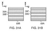
- Each external surface of the detector waveguideis divided into a first grid of strips interspersed with a second grid of strips.
- the first and second gridshave different light-modifying characteristics. Overlapping strips from the first grid of strips on each external surface are operative to waveguide light. Overlapping strips from the second grid of strips on each external surface are operative to absorb light scattered out of regions of the detector waveguide sandwiched by overlapping strips from the first grid of strips on each external surface.
- the stripsare orthogonal to the switchable grating columns.
- first grid of each external waveguide surfaceis one of clear or scattering and the second grid of at least one external waveguide surface is infrared absorbing.
- the beam steering meanscomprises: a first transmission grating layer; a half wavelength retarder layer overlaying the first transmission grating layer; a second transmission grating layer overlaying the half wavelength retarder layer; and a quarter wavelength retarder layer sandwiched by the second transmission grating layer and the platen.
- the external faces of the detector waveguide and the illuminator waveguideabut an air space or a low refractive index material layer.
- the first waveguide couplercouples light from the illumination means into the first TIR path in the illuminator waveguide.
- a switchable grating element of the illuminator waveguide in a diffracting statediffracts the first TIR path light towards the platen into a first beam direction.
- the beam steering meansdeflects the first beam direction light towards the platen in a second beam direction.
- An active column of the second switchable grating array along the third beam directiondiffracts the third angle light into a second TIR path in the detector waveguide.
- the second waveguide couplercouples the second TIR path light into an output optical path towards the detector.
- the first to third optical paths and the first and second TIR pathsare in a common plane.
- the first direction lighttraverses the detector waveguide.
- the second direction lighttraverses the illuminator waveguide.
- first to third optical paths and the first and second TIR pathsare in a common plane.
- FIG. 1is a schematic side elevation view of a contact image sensor in a first embodiment of the invention.
- FIG. 2is a schematic front elevation of the waveguiding structure used in the first embodiment of the invention showing the cross sections of the waveguide cores and cladding.
- FIG. 3Ais a schematic plan view of a first operational state of an SBG device used in a first embodiment of the invention.
- FIG. 3Bis a schematic plan view of a second operational state of an SBG device used in a first embodiment of the invention.
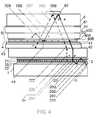
- FIG. 4is a schematic side elevation view of a contact image sensor in a first embodiment of the invention showing the principle ray paths.
- FIG. 5Ais a schematic side elevation view of a detail of the contact image sensor showing the ray propagation through the waveguide core and second SBG array in one embodiment of the invention.
- FIG. 5Bis a schematic side elevation view of a detail of the contact image sensor showing the ray propagation through the waveguide core and second SBG array in one embodiment of the invention.
- FIG. 6is a schematic plan view of a wave-guiding structure and detector module used in one embodiment of the invention.
- FIG. 7is a schematic plan view of a wave-guiding structure and detector module used in one embodiment of the invention.
- FIG. 8is a schematic plan view of a wave-guiding structure and detector module used in one embodiment of the invention.
- FIG. 9is a schematic side elevation view of a detection scheme based on terminating waveguides in the wave-guiding structure with an angled polished facet as used in one embodiment of the invention.
- FIG. 10is a schematic side elevation view of a detection scheme based on applying out coupling gratings to waveguides in the wave-guiding structure as used in one embodiment of the invention.
- FIG. 11is a schematic plan view of a detection scheme based on a two dimensional array used in one embodiment of the invention.
- FIG. 12Ais a schematic side elevation view of an illumination means in one embodiment of the invention.
- FIG. 12Bis a schematic plan view of an illumination means in one embodiment of the invention.
- FIG. 13is a schematic plan view of an illumination means in one embodiment of the invention.
- FIG. 14is a flow chart illustrating a method of making a contact image measurement in one embodiment of the invention.
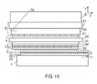
- FIG. 15is a schematic side elevation view of a contact image sensor in one embodiment of the invention.
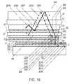
- FIG. 16is a schematic side elevation view of a contact image sensor in one embodiment of the invention showing the principle ray paths.
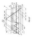
- FIG. 17is a schematic side elevation view of a contact image sensor in one embodiment of the invention.
- FIG. 18is a table showing typical refractive indices and layer thicknesses used in the first embodiment of the invention.
- FIG. 19is a schematic side elevation view of a contact image sensor in one embodiment of the invention.
- FIG. 20is a schematic diagram showing the key components a contact image sensor in one embodiment of the invention.
- FIG. 21is a schematic side elevation view of a detector waveguide in one embodiment of the invention.
- FIG. 22is a schematic side elevation view of a detector waveguide in one embodiment of the invention showing the coupling of signal light via an active element of the SBHG array.
- FIG. 23is a schematic plan view of a wave-guiding structure and detector module used in one embodiment of the invention.
- FIG. 24is a cross-sectional view showing a detail of a detector component using a SBG waveguiding structure in one embodiment of the invention.
- FIG. 25is a plan view of the SBG switching electrodes used in one layer of a detector component based a SBG waveguiding structure in one embodiment of the invention.
- FIG. 26is a plan view of the SBG switching electrodes used in one layer of a detector component based a SBG waveguiding structure in one embodiment of the invention.
- FIG. 27is a side elevation view of a contact image sensor in one embodiment of the invention in which the detector and illuminator components are performed by a single waveguide containing a single SBG array.
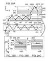
- FIG. 28Ais a side elevation view of a contact image sensor in one embodiment of the invention in which external surfaces of the detector waveguide are divided into interspersed grids of strips having different light-modifying characteristics to provide a multiplicity of parallel waveguiding paths.
- FIG. 28Bis a detail of the embodiment of FIG. 28A showing the interspersed grid of strips on a first external surface.
- FIG. 28Cis a detail of the embodiment of FIG. 28A showing the interspersed grid of strips on a first external surface.
- FIG. 28Dis a detail of the embodiment of FIG. 28A showing a cross section of the detector waveguide with beam cross sections.
- FIG. 29is a side elevation view of the detector waveguide in the embodiment of FIG. 28A showing a side view of the SBG array and the interspersed grids of strips applied to the external surface.
- FIG. 30is a front elevation view of the detector waveguide in the embodiment of FIG. 28A showing a cross section of the SBG array.
- FIG. 31Ashows an alternative configuration of the strips on a first external surface of the detector waveguide of FIG. 28A .
- FIG. 31Bshows an alternative configuration of the strips on a second external surface of the detector waveguide of FIG. 28A .
- FIG. 32shows alternative of strip configurations that may be used on the external surfaces of the detector waveguide of FIG. 28A .
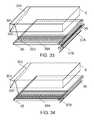
- FIG. 33is a schematic three dimensional view showing the platen and detector waveguide in one embodiment in which the detector waveguide is coupled to the detector by means of a micro lens array.
- FIG. 34is a schematic three dimensional view showing the platen and detector waveguide in one embodiment in which the detector waveguide is directly coupled to the detector.
- FIG. 35is a flow chart illustrating a method of making a contact image measurement using the apparatus of FIG. 28A .
- FIG. 36Ais a side elevation view of a contact image sensor in one embodiment of the invention in which the detector comprises a SBG array and a waveguide array and external surfaces of the waveguide array is divided into interspersed grids of strips having different light-modifying characteristics to provide a multiplicity of parallel waveguiding paths.
- FIG. 36Bis a detail of the embodiment of FIG. 36A showing a plan view of the interspersed grid of strips on the external surface.
- FIG. 36Cis a cross sectional view of the waveguide array in the embodiment of FIG. 36A .
- FIG. 37Ais a plan view of a first operational state of a two dimensional SBG array used in the at least one of the detector and illuminator waveguides in one embodiment.
- FIG. 37Bis a plan view of a second operational state of a two dimensional SBG array used in the at least one of the detector and illuminator waveguides in one embodiment of the invention.
- FIG. 38is a block diagram illustrating the key system modules of a software platform for use with a contact image sensor for finger print sensing in one embodiment of the invention.
- on-axisin relation to a ray or a beam direction refers to propagation parallel to an axis normal to the surfaces of the optical components described in relation to the invention.
- light, ray, beam and directionmay be used interchangeably and in association with each other to indicate the direction of propagation of light energy along rectilinear trajectories.
- gratingwill refer to a Bragg grating.
- switchable gratingwill refer to a Bragg grating that can be electrically switched between an active or diffracting state and an inactive or non-diffractive state.
- the preferred switchable gratingwill be a Switchable Bragg Grating (SBG) recording in a Holographic Polymer Dispersed Liquid Crystal (HPDLC) material.
- SBGSwitchable Bragg Grating
- HPDLCHolographic Polymer Dispersed Liquid Crystal
- a non switchable gratingmay be based on any material or process currently used for fabricating Bragg gratings.
- the gratingmay be recorded in a holographic photopolymer material.
- An SBGcomprises a HPDLC grating layer sandwiched between a pair of transparent substrates to which transparent electrode coatings have been applied.
- the first and second beam deflectorsessentially comprise planar fringe Bragg gratings. Each beam deflector diffracts incident planar light waves through an angle determined by the Bragg equation to provide planar diffracted light waves.
- SBGvolume phase grating
- PDLCpolymer dispersed liquid crystal
- SBG devicesare fabricated by first placing a thin film of a mixture of photopolymerizable monomers and liquid crystal material between parallel glass plates. Techniques for making and filling glass cells are well known in the liquid crystal display industry. One or both glass plates support electrodes, typically transparent indium tin oxide films, for applying an electric field across the PDLC layer. A volume phase grating is then recorded by illuminating the liquid material with two mutually coherent laser beams, which interfere to form the desired grating structure.
- PDLCpolymer dispersed liquid crystal
- the monomerspolymerize and the HPDLC mixture undergoes a phase separation, creating regions densely populated by liquid crystal micro-droplets, interspersed with regions of clear polymer.
- the alternating liquid crystal-rich and liquid crystal-depleted regionsform the fringe planes of the grating.
- the resulting volume phase gratingcan exhibit very high diffraction efficiency, which may be controlled by the magnitude of the electric field applied across the PDLC layer.
- an electric fieldis applied to the hologram via transparent electrodes, the natural orientation of the LC droplets is changed causing the refractive index modulation of the fringes to reduce and the hologram diffraction efficiency to drop to very low levels resulting in for a “non diffracting” state.
- the electrodes and the circuits and drive electronics required to perform switching of the SBG elementsare not illustrated in the Figures.
- Methods for fabricated patterned electrodes suitable for use in the present inventionare disclosed in PCT US2006/043938. Other methods for fabricating electrodes and schemes for switching SBG devices are to be found in the literature.
- the present inventiondoes not rely on any particular method for fabricating transparent switching electrodes or any particular scheme for switching arrays of SBGs.
- the descriptionmakes reference to SBG arrays the invention may be applied using any type of switchable grating.
- a contact image sensoris illustrated in the schematic side elevation view of FIG. 1 .
- the apparatuscomprises the following parallel optical layers configured as a stack: an illumination means 1 for providing a collimated beam of first polarized light; a first SBG array device 2 further comprising first and second transparent substrates 21 , 22 sandwiching an array 20 of selectively switchable SBG column elements, and ITO electrodes 20 A, 20 B applied to opposing faces of the substrates, the SBG substrates together providing a first TIR light guide for transmitting light in a first TIR beam direction; an air gap 23 ; a transmission grating 43 ; a third transparent substrate (low index glue layer 42 ; a low refractive index SBG cover glass 41 ; a ITO layer 40 B; a second SBG array device 4 comprising an array of selectively switchable SBG column elements; a ITO layer 40 B; a barrier film 40 C; a waveguiding layer 50 comprising a multiplicity of waveguide cores separated by cladding material having a generally
- Each core of the waveguide structureis optically couple to an element of a detector array.
- the apparatusfurther comprises: means for coupling light from the illumination means into the first TIR light guide; means for coupling light out of the core into an output optical path; and a detector comprising at least one photosensitive element, the photosensitive element being optically coupled to at least one the core.
- the illumination meansmay further comprise optical stops to eliminate stray light and scatter.
- the first polarized lightmay be either S or P polarized. Since SBGs recorded in the inventors preferred HPDLC material system are P-polarization sensitive that polarization will be assumed for the purposes of describing the invention.
- the transmission grating 43is advantageously a conventional transmission Bragg grating recorded in a holographic photopolymer. However, other equivalent means for providing a transmission grating may be used. Desirably, the contact image sensor uses infrared light from at least one laser. In one embodiment of the invention the light wavelength is 785 nanometers.
- FIG. 2A cross sectional view (in the XZ plane) of the waveguiding structure is shown in FIG. 2 which illustrates the waveguiding structure 40 sandwiched by the barrier film 40 C and the clad layer 51 (or bottom buffer). A core 71 and a region of cladding 72 between adjacent cores is indicted in the drawing.
- the first SBG device 20comprises an array of strips or columns aligned normal to the light propagation direction of the TIR light.
- the second SBG arrayalso comprises an array of strips or columns aligned parallel to the strips in the first SBG device.
- the SBGs in the first and second SBG arraysare recorded as single continuous element in each case.
- Transparent electrodesare applied to the opposing surfaces of the substrates 21 , 22 with at least one electrode being patterned to define the SBG elements.
- each SBG element in the first and second SBG arrayshas a diffracting state when no electric field is present across the ITO electrodes and a non-diffracting state when an electric field is present across the ITO electrodes, the SBG elements diffracting only the first polarization light.
- Transparent electrodesare applied to the opposing faces of the third transparent substrate and the waveguiding layer with at least one electrode being patterned to define the SBG elements.
- the first SBG arrayhas a resolution of 1600 elements.
- the resolution of the second SBG arrayis lower, typically 512 elements.
- the column elements of the first and second SBG arrayshave longer dimensions disposed orthogonally to the first TIR beam direction.
- the elements of the second SBG device which are in a non-diffracting statehave a generally lower refractive index than the waveguide cores.
- the third transparent substratehas a generally lower refractive index than the cores.
- the air gap 23may be replace by a refracting material layer.
- the second SBG array 4acts as the lower cladding layer of the wave guiding structure while the waveguide core 50 and the third transparent substrate 41 act as the containing substrates of the second SBG array device 4 .
- the first and second transparent substrates 21 , 22 sandwiching the first SBG arraytogether provide a first TIR light guide with the TIR occurring in the plane of the drawing.
- the second SBG array device 4is sandwiched by the waveguide core and the third transparent substrate 41 which form a second TIR light guide.
- the contact image sensorfurther comprises a means 11 for coupling light from said illumination means 1 into the first SBG array lightguide.
- the inventiondoes not assume any particular coupling means.
- One particular solution discussed lateris based on prismatic elements.
- the coupling meansmay be based on gratings.
- the contact image sensorfurther comprises a means for coupling light out of the wave-guiding structure into an output optical path leading to a detector.
- the coupling meanswhich schematically represented by the dashed line 52 is advantageously a grating device which will be discussed in more detail later.
- the column elements of the first and second SBG arraysare switched sequentially in scrolling fashion, backwards and forwards.
- the SBG elementsare switched sequentially across the SBG array and only one SBG element in each array is in its diffracting state at any time. The effect is to produce a narrow scanning column of light that sweeps backwards and forwards across the platen.
- FIGS. 3A-3Bwhich provides schematic plan views of the SBG array 20 at two consecutive switching states.
- the SBG element indicated by 25is in its diffracting state and all other SBG elements are in their non diffracting states, allowing TIR light to be transmitted through the arrays without substantial transmission loss or path deviation.
- the SBG element 24is switched to its non-diffracting stated while the adjacent element 25 is switched to its diffracting state.
- Incident light 200 from the illuminator means 1is coupled into the first SBG device 2 by a coupling means indicated by 11 which will be discussed below.
- the lightundergoes TIR in the light guide formed by the substrates 21 , 22 as indicted by the rays 201 - 203 .
- the active (i.e. diffracting) SBG column element 23diffracts light 204 out of the light guide.
- the light 204is now diffracted by the transmission grating into the ray 206 which propagates towards the platen without significant deviation or loss through the intervening optical layers.
- the symbol Pindicates that the light is P-polarized, i.e. it retains the polarization of the input laser light.
- the fingersare placed onto the scanner surface.
- the light incident on the platen outer surfaceis totally internally reflected downwards towards the wave guiding structure 50 and then on to the detector.
- the finger skin touching the platen surfacecauses reflection at the outer surface of the platen to be frustrated such that light leaks out of the platen.
- the parts of the finger skin that touch the platen surfacetherefore becomes the dark part of the finger print image because light never makes it to the detector array.
- the X coordinate of the contacting featureis given by the detector array element providing the dark-level or minimum output signal. The latter will be determined by the noise level of the detector.
- the Y coordinate of the contacting featureis computed from the geometry of the ray path from the last SBG element in the first SBG array that was in a diffracting state just prior to TIR occurring in the platen and a signal from the reflected light being recorded at the detector.
- the ray pathis computed using the diffraction angle and the thicknesses and refractive indices of the optical layers between the SBG element and the platen surface.
- an alternative detection schemeis based on the principle that in the absence of any external pressure art the platen/air interface the incident light is transmitted out of the platen.
- external pressure from a body 62 of refractive index lower than the platencauses the light to be totally internally reflected downwards towards the wave guiding structure 50 .
- the X coordinate of the contacting featureis now given by the detector array element providing the peak output signal.
- the procedure for computing the Y coordinateremains unchanged.
- SBGwhen in the state designated as “non-diffracting” will, in practice, have a very small refractive index modulation and will therefore diffract a small amount of light. This residual diffraction is negligible in most applications of SBGs. However, in applications such as the present invention any residual refractive modulation will result in a small amount of light being diffracted out of the light guide. For example referring to FIG. 4 , SBG elements such as 24 will have a small diffraction efficiency leading to a small portion of TIR light being diffracted upwards into the ray path represented by the dashed lines and the ray directions indicated by 220 - 223 .
- This lightwill follow a parallel oath to the light from the active SBG element (the signal light) and will be reflected off the platen outer surface towards the waveguides. Coupling of this stray light into the waveguides, where it will contribute a background leakage noise to the output signal, is prevented by switching the second SBG array elements in synchronization with the first array elements such that only the element of the first and second SBGs array lying on the signal ray path are in a diffracting state at any time.
- the readout of the signal from detector arrayis in turn synchronized with the switching of the elements of the first and second SBG arrays.
- the wave guiding structure 50 and the SBG array 4together provide the means for coupling light out of the sensor onto a detector array.
- the SBGprovides the lower cladding and the layer 51 provides the upper cladding.
- the coupling of light into the waveguiderelies on the second SBG array which acts as a switchable cladding layer as will be discussed below.
- the second SBG arrayis operated in a similar fashion to the first SBG array with column elements being switched sequentially in scrolling fashion, backwards and forwards. Only one SBG element is in a diffracting state at any time.
- the non active elementsperform the function of a clad material.
- the role of the active SBG elementis to steer incident ray into the TIR angle.
- FIG. 5Ashows a detail of the wave guiding structure including the cladding 51 , core 50 , second SBG array 4 and SBG substrate 41 . Note that in FIGS. 5A-5B the layers 40 A, 40 B, 40 C are not illustrated.
- the SBG gratingis represented by the single Bragg fringe 44 .
- the ray 207 on entering the active SBG element 43 at an incidence angle wis diffracted into the ray 207 A.
- the deflection of the rayis determined by the Bragg diffraction equation. Since the average index of the SBG medium is higher than that of the substrate layer 41 the diffracted ray 207 A undergoes TIR within the SBG medium and the reflected ray 208 propagates into the core at an angle u which is slightly higher than the critical angle of the core/cladding interface.
- the angle uis determined by the slant angles of the Bragg fringes and the incidence angle w.
- the ray 208undergoes TIR to give the downward ray 209 which enters the non diffracting SBG element 45 at the angle u as the ray 210 .
- the ray 210undergoes TIR at the interface of the SBG element/third substrate and re-enters the core as the ray 211 which from reflection symmetry is at angle u. This process is repeated along the waveguide until the light is coupled out towards the detector. Since all of the remaining SBG elements along the waveguide path are in their non diffracting states TIR between the cladding layer and the SBG lower substrate continues until the light is couple out of the waveguide towards the detector.
- the inventionalso covers the case where the SBG substrate abuts a low index slab 42 which has a lower index than the third substrate.
- the layer 42is not essential in all applications of the invention but will in general provide more scope for optimizing the optical performance of the sensor. Referring to FIG. 5B it will be seen that the ray paths are similar to those of FIG. 5A except that the TIR of the diffracted ray 207 A now takes place at the interface between the substrate 41 and the low index slab 42 .
- the diffracted ray 207 Ais transmitted into the substrate 41 as the ray 207 B and undergoes TIR into the ray 207 C at the low index layer after transmission through the substrate 41 and the SBG array 4 the ray now indicated by 208 A propagates into the core at an angle v which is slightly higher than the critical angle of the core/clad interface.
- the ray 208 Aundergoes TIR to give the downward ray 209 A which enters the non activated SBG element 45 as the ray 210 A.
- the ray 210 Aundergoes TIR at the low index layer and re-enters the core as the ray 211 A which from reflection symmetry is at angle v. This process is repeated along the waveguide until the light is coupled out towards the detector. It should be appreciated that in situations where the collimation of the beam is not very tightly controlled it is possible that TIR may occur at the SBG substrate index for some rays and at the low index slab substrate for other rays.
- the third transparent substratehas a generally lower refractive index than an element of the second SBG array in its diffracting state.
- the third transparent substratehas a generally lower refractive index than the element of the second SBG array in its non-diffracting state.
- the cleared SBGwill still have a small residual refractive index modulation which causes a small amount of the incident light to be diffracted.
- the direction of diffractionwill depend on the TIR angle. In some cases the ray may not be at the Bragg angle but may still be sufficiently close to the Bragg angle to be diffracted, but with a lower diffraction efficiency. If not diffracted it may end up in the TIR beam, thereby contributing to the output signal.
- the wave-guiding structure 50which is illustrated in schematic plan view in FIG. 1 and in cross section in FIG. 2 comprises a multiplicity of parallel strip waveguides generally indicated by 70 , the waveguide core element of one of the waveguides and the surrounding cladding being indicated by numerals 71 , 72 .
- the inventiondoes not assume any particular waveguide geometry or material for fabricating the waveguiding layer. It should be apparent to those skilled in the art of integrated optics that a large number of different core/cladding combinations may be used in the invention.
- the corewill have a refractive index of typically between 1.51 to 1.56 or and the cladding layers will have refractive indices in the range from 1.41 to 1.47.
- the coremay be rectangular with cross sectional dimensions of 25-40 microns in depth ⁇ 40 microns in width.
- the coresmay have much larger or much smaller cross sectional dimensions subject to the specifications for coupling efficiency, waveguide crosstalk and other waveguide parameters set by the application.
- the wave-guiding structuremay use a polymer waveguide core of index typically in the range 1.50 to 1.60 with cladding index typically 1.45 to 1.55.
- the inventiondoes not assume any particular waveguide optical materials.
- the waveguide cladding in the waveguiding layer 51 and the cladding layer 51may be fabricated from one material. In some cases it may be advantages to have more than one cladding material in order to provide better control of the guide wave mode structure.
- the highest refractive index UV curable material suitable for use as either core or cladding in a high transparency waveguiding structure of the type required in the inventionis believed to have a refractive index of about 1.56 at 633 nm.
- the indexmight be slightly lower at longer wavelength.
- the problem with index values above about 1.56is that the materials become either colored or slightly metallic and hence lose their transparency. Higher index transparent materials exist but they are not UV curable, which makes them unsuitable for waveguide fabrication using currently available embossing process.
- FIGS. 6-8provides schematic plan views of alternative schemes for coupling the wave guiding structure 50 to the detector 8 .
- the detectorcomprises at least one element.
- a multiplicity of waveguide coresis generally indicated by 70 with a typical core element 71 and the surrounding cladding 71 being indicated in each case. Each core terminates at a coupler linked to a detector element.
- the ray paths from the active SBG element 23 to the waveguide terminationare indicated by 206 , 207 , 213 using the numerals of FIG. 4 .
- the detector 8is a linear array of elements such as 81 .
- a ray path from the waveguide termination to the detectoris indicated by 214 .
- the coresare each terminated by a 45 degree facet with directs light upwards or downwards (relative to the drawing surface) towards the detector along direction 214 which should be read as normal to the plane of the drawing.
- the detector pitchmatches the core spacing.
- a parallel path waveguide routing elementmay be provided between the waveguide termination and the detector. In the embodiment of FIG.
- the output light paths generally indicated by 502 from the waveguidesare converged onto a linear detector array that is much smaller than the width of the platen by means convergent path waveguide routing element 84 A.
- the coresare terminated by a 45 degree facet which directs the light upwards or downwards.
- the output light paths generally indicated by 503 from the waveguidesare converged by means of a convergent path waveguide routing element 85 onto a single element detector 83 .
- the coresare terminated by a 45 degree facet which directs the light upwards or downwards.
- the apparatusmay further comprise a micro lens array disposed between the waveguide ends and the detector array where the micro lens elements overlap detector elements.
- FIG. 9is a schematic side elevation view of one method of coupling light out of the wave-guiding structure in which there is provided a 45 degree facet 86 A terminating each waveguide element in the wave-guiding structure.
- FIG. 9may be a cross section of any of the schemes illustrated above.
- the detector 8 and the waveguide cladding layers 75 , 76 and core 74are illustrated.
- the core 74may be a continuation of one of the cores 70 or a core of material of similar optical properties optically coupled to one of said cores 70 .
- the cladding layermay be a continuation of the cladding layer 51 in FIG. 1 and FIG. 3 or material of similar refractive index.
- the cladding layermay be continuation of the HPDLC material of the SBG array 4 or material of similar refractive index to the SBG array in its non-active state.
- FIG. 10is a schematic side elevation view of another method of coupling light out of the wave-guiding structure in which a grating device 86 B is applied to each waveguide element.
- FIG. 10may be a cross section of any of the schemes illustrated in FIGS. 7-9 .
- the gratingmay be a surface relief structure etched into the waveguide cladding. Alternatively, the grating may be a separate layer in optical contact with one or both of the core or cladding. In one embodiment of the invention the grating may be recorded into a cladding layer as a Bragg grating.
- the detector 8is a linear array.
- the detector elementsare distributed over two dimensions. This avoids some of the alignment problems of coupling waveguide elements to detector elements with a very high resolution linear array.
- the waveguides from the wave-guiding structure generally indicated by 87are fanned out in the waveguide groups 87 A, 87 C.
- the detectorsare generally indicated by 88 .
- the waveguide groups 87 A, 87 Ccontain waveguide cores such as 87 B which overlays the detector 88 B in the detector group 88 A and waveguide 87 D which overlays the detector 88 D in the detector group 88 C.
- the waveguide to detector computingmay employ 45 degrees core terminations, gratings, prisms or any other methods known to those skilled in the art. From consideration of FIG. 11 it should be apparent that many alternative configurations for coupling the waveguiding structure to a two dimensional detector array are possible.
- the beams produced by the illumination meanswill not be perfectly collimated even with small laser die and highly optimized collimating optics. For this reason the interactions of the guided beams with the SBG elements will not occur at the optimum angles for maximum Bragg diffraction efficiency (DE) leading to a small drop in the coupling efficiency into the waveguiding structure.
- DEBragg diffraction efficiency
- the reduction in signal to noise ratio (SNR) resulting from the cumulative depletion of the beam by residual gratings along the TIR path in the output waveguidemay be an issue in certain applications of the invention.
- a trade-offmay be made between the peak and minimum SBG diffraction efficiencies to reduce such out-coupling.
- the inventorshave found that minimum diffraction efficiencies of 0.02% are readily achievable and efficiencies as low as 0.01% are feasible.
- a small amount of diffusion( ⁇ 0.1%) can be encoded into the SBG to provide a broader range of angles ensuring that guided light is not all at the Bragg angle.
- a small amount of diffusionwill be provided by scatter within the HPDLC material itself. Further angular dispersion of the beam may also be provided by etching both the ITO and the substrate glass during the laser etching of the ITO switching electrode.
- the refractive index modulation of second SBG arrayis varied along the length of the array during exposure to provide more uniform coupling along the waveguide length.
- the required variationmay be provided by placing a variable neutral density filter in proximity to the SBG cell during the holographic recording. In any case the power depletion along the waveguide can be calibrated fairly accurately.
- the SBG arraycomprises a continuous grating with the individual elements being defined by the electrode patterning.
- the gaps between the elements of the first SBG arraysshould therefore be made as small as possible to eliminate stray light which might get coupled into the waveguiding layer reducing the SNR of the output signal.
- the gapshould be not greater than 2 micron.
- the noise signal contributed by the gapsis integrated over the area of an active column element of the second SBG array element while the light contributing to the useful signal is integrated over the simultaneously active column element of the first SBG array.
- SNRSNR should be higher than 100.
- the transparent electrodesare fabricated from PDOT (poly ethylenedioxythiophene) conductive polymer.
- PDOTpoly ethylenedioxythiophene
- This materialhas the advantage of being capable of being spin-coated onto plastics.
- PDOT (and CNT)eliminates the requirement for barrier films and low temperature coating when using ITO.
- a PDOT conductive polymercan achieve a resistivity of 100 Ohm/sq.
- PDOTcan be etched using Reactive Ion Etching (RIE) processes.
- RIEReactive Ion Etching
- the first and second SBG arraysare switched by using a common patterned array of column shaped electrodes.
- Each element of the second SBG array, which is of lower resolution than the first SBG arrayuses subgroups of the electrode array.
- the waveguidesare fabricated from PDOT. The inventors believe that such a waveguide will exhibit high signal to noise ratio (SNR).
- the waveguidesare fabricated from CNT using a lift-off stamping process.
- An exemplary CNT material and fabrication processis the one provided by OpTIC (Glyndwr Innovations Ltd., St. Asaph, Wales, and United Kingdom).
- the waveguide coresare conductive photopolymer such as PDOT or CNT. Only the portions of the SBG array lying directly under the waveguide cores are switched. This avoids the problems of crosstalk between adjacent waveguide cores thereby improving the SNR at the detector.
- the TIR angle in the platendepends on the refractive indices of the platen glass and the thin layer of water (perspiration) between the subject's skin and the platen.
- the platenis made from SF11 glass the refractive index at 785 nm is 1.765643, while the index of water at 785 nm is 1.3283.
- the arc-sine of the ratio of these two indices(sin-1 (1.3283/1.76564) gives a critical angle of 48.79°. Allowing for the salt content of perspiration we should assume an index of 1.34, which increases the critical angle to 49.37°.
- the TIR angle at the platenshould be further increased to 50° to provide for alignment tolerances, fabrication tolerances, and water variations as well as collimation tolerances too for less than perfect lenses and placements of these parts.
- other materialsmay be used for the plate. It is certainly not essential to use a high index to achieve moisture discrimination.
- the choice of platen materialwill be influenced by the need to provide as large a bend angle as possible at the SBG stage. The reason for this is that higher diffraction efficiencies occur when the bend angle (i.e. the difference between the input angle at the SBG and the diffracted beam angle) is large. Typically bend angles in the region of 20-25° are required.
- the platenmay be fabricated from a lower refractive material such as Corning Eagle XG glass which has a refractive index of 1.5099.
- This materialhas the benefit of relatively low cost and will allow a sufficiently high TIR angle to enable salty water discrimination. Assuming the above indices for perspiration (salt water) of 1.34 and water of 1.33 the critical angle for salt water is 62.55777° and the critical angle for water of 61.74544°.
- the indices of the SBG substrates and the element 42are all chosen to be 1.65 and the platen index is chosen to be 1.5099.
- the material used in the low index layer 42is equal in index to the SBG substrates, or slightly lower.
- the TIR angle in the SBG layeris 78 degrees. At this index value the diffracted beam angle with respect to the surface normal within the upper SBG substrate will be 55 degrees. For a TIR angle of 78 degrees in the SBG the effective diffraction bend angle is 23 degrees.
- the TIR angle in the platen based on the above prescriptionis 63.5 degrees allowing for typical refractive index tolerances (i.e. a 0.001 refractive index tolerance and 0.3 degree minimum margin for glass tolerances).
- n ⁇ sin (U)constant where n is the refractive index and U is the refraction angle.
- FIG. 1there is an air gap between the first SBG array 2 and the transmission grating.
- Other air gapsmay be provided between other layers in the sensor architecture subject to the restrictions imposed by the Snell invariant and the diffraction bend angle as discussed above.
- the inventionrequires tight control of refractive index and angle tolerances to maintain beam collimation otherwise cross talk between adjacent waveguides may occur leading to output signal ambiguities.
- Index variationsof 0.001 may lead to TIR boundaries shifting by around 0.25° for example.
- Angular tolerancesare typically 0.1° in transmission. At reflection interfaces the angular error increases. In the worst case a ray will experience reflections off five different surfaces.
- the TIR paths used in the sensorcan typically undergo up to 18 bounces.
- the effects of a wedge angle in the substrateswill be cumulative. For example, a 30 seconds of arc wedge may lead to a 0.3° error after 18 bounces. Desirably, the cumulative angular errors should allow a margin for TIR of at least 1°.
- Typical refractive indices and layer thicknesses used in the embodiment of FIG. 1are provided in the table of FIG. 18 .
- FIG. 12illustrates the illumination module of the contact image sensor in one embodiment in more detail.
- FIG. 12Ais a schematic side elevation view showing the illumination means and the SBG device in one embodiment of the invention.
- FIG. 12Bprovides a side elevation view of the same embodiment of the invention.
- the wave guiding structureis not illustrated in FIG. 12A .
- the illumination meanscomprises a multiplicity of lasers indicated by 13 A- 13 D providing separate parallel illumination modules, each module comprising a pair of crossed cylindrical lenses such as 16 A, 16 B a light guide 17 , transparent slabs 12 , 19 and transparent substrate 13 .
- the slabs 12 , 19abut the first SBG array 2 comprising the transparent substrates 21 , 22 sandwiching the SBG layer 20 .
- the lenses 16 A, 16 Bmay be crossed cylindrical lenses such that the first lens 16 A collimates the input light 101 A to provide a first beam 102 A that is collimated in a first plane and the second lens 16 B collimates the beam 102 A in the orthogonal plane to provide a beam 103 A collimated in a second plane orthogonal to the first plane such that the resulting beam in the light guiding element 17 is collimated in both beam planes.
- the lensesare of rectangular cross section.
- the beams from the lasers 13 A- 13 Dare identical and abut to form a continuous rectangular beam extending over an area substantially the same as the first SBG array in plan view.
- the lightguide element 17comprises a transparent slab with a planar input surface orthogonal to the beam direction and a reflecting surface 14 at an angle to the beam direction.
- the surface 14reflects the beam 104 A into the direction 105 A orthogonal to 104 A.
- the slab portions 12 and 19are illustrated as being air separated they may abut.
- the slab 12has a tilted reflecting surface 18 for directing light 106 A into the SBG array device 2 .
- the slab 12has an identical refractive index to the substrates 21 , 22 sandwiching the SBG array 20 .
- the slab 19essentially performs the function of a spacer.
- the slab 13also acts as spacer.
- the slab 13is coated with a polarization selective coating in the region illuminated by the upward propagating light reflected off the mirror surface 14 .
- the refractive index of the slab 19is chosen to ensure that rays such as 106 A, 107 A entering the first SBG array device exceed the critical angles for TIR within the light guide formed by the first SBG array device.
- the reflective surfaces 14 , 18essentially provide the coupling means indicated schematically by the symbol 11 in FIG. 1 . It should be apparent to those skilled in the art of optical design that in other embodiments of the invention other equivalent optical configurations including diffractive optical surfaces may be used to perform the function of the surfaces 14 and 18 .
- the SBG arrayan average refractive index of 1.55 in its non-diffractive state and 1.62 when in a diffracting state.
- the substrates 21 , 22have refractive indices of 1.55.
- the slab 12has an index of typically between 1.5 and 1.7 to match the SBG substrates.
- the slab 19is advantageously a polymer material of refractive index 1.49. The resulting critical angle in the first TIR light guide formed by the first array SBG device is therefore approximate 74 degrees.
- the illumination meanscomprises a single laser 13 E and a collimator lens system comprising the crossed cylindrical lenses 46 a , 46 b .
- the said illumination meansprovides a single collimated beam of rectangular cross section 104 E.
- a sensor according to the principles of the present applicationmay fabricated using the HPDLC material system and processes disclosed in PCT Application No.: PCT/GB2012/000680 entitled IMPROVEMENTS TO HOLOGRAPHIC POLYMER DISPERSED LIQUID CRYSTAL MATERIALS AND DEVICES which is incorporated by reference herein in its entirety.
- the SBG substratesmay fabricated from polycarbonate, which is favored for its low birefringence.
- Two other currently available plastic substrates materialsare a cyclic olefin copolymer (COC) manufactured by TOPAS Advanced Polymers and sold under the trade name TOPAS.
- the otherwas a cyclic olefin polymer (COP) manufactured by ZEON Corporation and sold under the trade names ZEONEX and ZEONOR. These materials combine excellent optical properties (including high transmission and low birefringence) with excellent physical properties (including low specific gravity, low moisture absorption, and relatively high glass transition temperature).
- COPcyclic olefin polymer
- the inventorshave found that an adequate diffraction efficiency (i.e. ⁇ 70%) can be obtained when using plastic substrates.
- the diffraction efficiencycompares favorably with glass.
- the switching time of plastic SBGis also found to be sufficient to produce satisfactory devices.
- Transparent conductive (ITO) coatings applied to the above plasticshave been found to be entirely satisfactory, where satisfactory is defined in terms of resistivity, surface quality, and adhesion. Resistivity values were excellent, typically around 1000/square. Surface quality (i.e., the size, number and distribution of defects) was also excellent. Observable defects are typically smaller than 1 micron in size, relatively few in number, and sparsely distributed. Such imperfections are known to have no impact on overall cell performance. ITO suffers from the problem of its lack of flexibility. Given the rugged conditions under some SBG devices may operate, it is desirable to use a flexible TCC with a plastic substrate. In addition, the growing cost of indium and the expense of the associated deposition process also raise concerns.
- Carbon nanotubesare one possible alternative to ITO. If deposited properly, CNTs are both robust and flexible. They can be applied much faster than ITO coatings, are easier to ablate without damaging the underlying plastic, and exhibit excellent adhesion. At a resistivity of 200 ⁇ /sq, the ITO coatings on TOPAS 5013S exhibit more than 90% transmission. At a resistivity of 230 ⁇ /sq, the CNT coatings deposited on the same substrates material exhibited more than 85% transmission. It is anticipated that better performance will results from improvements to the quality and processing of the CNTs.
- An adhesion layeris required to support the transparent conductive coating.
- the inventorshave found that the adhesion of ITO or CNT directly to plastics such as TOPAS and ZEONEX was poor to marginal. The inventors have found that this problem can be overcome by means of a suitable adhesion layer.
- One exemplary adhesion layeris Hermetic TEC 2000 Hard Coat from the Noxtat Company. This material has been found to yield a clear, mar-resistant film when applied to a suitably prepared plastic substrate. It can be applied by flow, dip, spin, or spray coating. TEC 2000 Hard Coat is designed to give good adhesion to many thermoplastic substrates that are cast, extruded, molded or blow molded.
- TEC 2000When applied to TOPAS, ZEONEX or other compatible plastics, the strength and break resistance provided by TEC 2000 is nearly as scratch and abrasion resistant as glass. Hermetic Hard Coat forms a transparent 3-6 micron film on plastic surfaces. The Refractive index of the coating is 1.4902.
- a sample of TOPAS plastic sheet coated with TEC 2000 Noxtat protective Hard Coatis shown in FIG. 13 .
- the next step in SBG cell production processis applying the TCC (ITO or CNT) to the hard coat.
- FIG. 14shows Noxtat Hard Coat samples with additional ITO and CNT coatings.
- the Hard Coatplays two roles in SBG cell production. One is to increase adhesion of the conductive layer to the plastic and prevent degassing during vacuum coating. The second role is to seal the plastic surface from environmental influence. It was found that TEC 2000 Hard Coat performs very well with TOPAS and ZEONEX materials.
- a fundamental feature of SBGs fabricated using current HPDLC material systemsis that the grating is present when the device is in its passive state. An electric field must be applied across the HPDLC layer to clear the grating.
- An alternative HPDLC material systemthat may be used with the present invention provides a reverse mode SBG in which the grating is clear when in its passive state. A reverse mode SBG will provide lower power consumption. Reverse mode SBG devices are disclosed in PCT Application No.: PCT/GB2012/000680.
- FIG. 14A method of a method of making a contact image measurement in one embodiment of the invention in accordance with the basic principles of the invention is shown in the flow diagram in FIG. 14 . Referring to the flow diagram, we see that the said method comprises the following steps:
- an apparatuscomprising the following parallel optical layers configured as a stack: an illumination means for providing a collimated beam of first polarization light; a first SBG array device further comprising first and second transparent substrates sandwiching an array of selectively switchable SBG column elements, and ITO electrodes applied to opposing faces of the substrates and the SBG substrates together providing a first TIR light guide for transmitting light in a first beam direction; an air gap; a transmission grating; a third transparent substrate (low index glue layer); a SBG cover glass; a ITO layer; a second SBG array device comprising array of selectively switchable SBG column elements; a ITO layer; a barrier film; a waveguiding layer comprising a multiplicity of waveguide cores separated by cladding material having a generally lower refractive index than the cores, the cores being disposed parallel to the first beam direction; an upper clad layer having a generally lower refractive index than the cores (also referred to as the bottom buffer); a prim
- step 502sequentially switching elements of the first SBG array into a diffracting state, all other elements being in their non-diffracting states;
- step 503sequentially switching elements of the second SBG array into a diffracting state, all other elements being in their non-diffracting states;
- step 505the transmission grating diffracting the first optical path light upwards into a second optical path
- step 506a portion of the second optical path light incident at the point on the platen being transmitted out of the platen and light incident on the outer surface of the platen in the absence of said contact with an external material being reflected downwards in a third optical path, said third optical path traversing said cores,
- step 508an active SBG element of the second SBG array along the third optical path diffracting the third angle light downwards into a fourth optical path
- the fourth optical path lightbeing reflected upwards into a fifth optical path at the third substrate, the fifth optical path light exceeding the critical angle set by the core/clad interface and the critical angle set by one of the core/second SBG array or second SBG array/third substrate interfaces, and proceeding along a TIR path to the detector.
- the first to fifth optical paths in the method of FIG. 14lie in a plane orthogonal to the first SBG array.
- the method of FIG. 14further comprises the step of providing a transparent slab of index lower than the third transparent substrate disposed between the third substrate and the transmission grating, such that the fourth optical path light is reflected upwards at the substrate into a fifth optical path and the fifth optical path light exceeds the critical angle set by the core/clad interface and the critical angle set by one of the core/second SBG array, second SBG array/third substrate or third substrate/slab interfaces, providing a TIR path to the detector.
- a contact image sensoris illustrated in the schematic side elevation view of FIG. 15 .
- the apparatusis identical to that of FIG. 1 but further comprises a half wave retarder array 3 disposed between the air gap 15 and the transmission grating 43 .
- the half wave retarder array 3comprises an array of column-shaped elements 30 sandwiched by transparent substrates 31 , 32 .
- Each retarder element in the half wave retarder arrayis switchable between a polarization rotating state in which it rotates the polarization of incident light through ninety degrees and a non polarization rotating state.
- the column elements of the half wave retarder arrayhave longer dimensions disposed parallel to the Y-axis i.e. orthogonally to the first TIR beam direction. Each half wave retarder array element overlaps at least one strip element of the first SBG array. At any time one element of the first SBG array is in a diffracting state and is overlapped by an element of the half wave retarder array in its non-polarization rotating state, one element of the second SBG array is in a diffracting state, all other elements of the first and second SBG arrays are in a non-diffracting state and all other elements of the half wave retarder array are in their polarization rotating states.
- the function of the half wave retarder arrayis to control stray light such as that indicated by the ray 220 which is diffracted by the residual refractive index modulation of the element 24 .
- the switchable half wave retarder arraysolves the problem of background leakage noise by converting unwanted light at source into S-polarized light.
- the active (i.e. diffracting) SBG column element 23diffracts light 204 out of the light guide through the element 33 of the half wave retarder array 30 array as light 205 . Since the element 33 is in its non-polarization rotating state the light 205 remains P-polarized. Note that all other elements of the half wave retarder array are in their polarization rotating states.
- the diffracted ray 220is transmitted through the half wave retarder element 34 which is in its polarization rotating state such that the P-polarized light 220 is converted into S-polarized light 221 .
- the ray 221is next diffracted into the ray 222 by the transmission grating 43 .
- the ray 223is reflected off the platen/air interface into a downwards path as the ray 223 . Since the ray 223 is S-polarized it is not diffracted by the second SBG and is therefore not coupled into the waveguide path to the detector.
- the light 223propagates downwards though the stack of optical layers until it emerges from the bottom of the illuminator means 1 and is absorbed by a light-trapping means which is not illustrated. Typically, the light-trapping means would be an absorber.
- Other means for disposing of light of the type represented by the ray 223will be apparent to those skilled in the art of optical design. The invention does not assume any particular means for disposing of such stra
- FIG. 17there is provided a means for contact imaging of an object that emits light of a second wavelength when illuminated by light of a first wavelength.
- the apparatus of FIG. 17is identical to the sensor FIG. 4 except that in FIG. 15 the rays 237 , 238 , 239 which replace the ray 207 , 208 , 209 of FIG. 4 now correspond to second wavelength light emitted from the object 63 which is in contact with the platen and illuminated by first wavelength light 206 .
- the object 63may be a fluorescent material excited by UV radiation.
- the ray 243 which replaces the ray 223 of FIG. 4again represents a stray light path. It should be noted that the embodiment of FIG.
- FIG. 18is a table of the optical prescriptions of each layer (refractive index at 785 nm. and layer thickness in microns) of a typical implementation of the embodiment of FIG. 1 .
- Each layeris reference by the numerals used in FIG. 1 .
- many other combinations of layer materials and thicknessmay be used.
- the contact sensoressentially comprises three modules: a scanner a detector and the platen. These components are illustrated in FIGS. 19-20 in which FIG. 19 is essentially FIG. 1 with the components comprising the detector layer 9 (that is the second SBG array 4 and the waveguiding 5 ) contained in a dashed line box.
- the platencomprises the illuminator module and the first SBG array device 2 .
- the contact sensorcomprises the following parallel optical layers configured as a stack: an illumination means for providing a collimated beam of first polarization light; a first SBG array device further comprising first and second transparent substrates sandwiching an array of selectively switchable SBG column, and transparent electrodes applied to opposing faces of the SBG substrates together providing a first TIR light guide for transmitting light in a first TIR beam direction; and a transmission grating; and a platen, as illustrated in FIG. 1 but not shown in FIGS. 21-26 .
- the second SBG array devicefurther comprising third and fourth transparent substrates 46 A, 46 B sandwiching the SBG layer which is generally indicated by 48 and will be explained in more detail next.
- the layeressentially consists of a multiplicity of high index HPDLC regions separated by low index HPDLC regions. Patterned transparent electrodes 47 A, 47 B are applied to opposing faces of the substrates.
- the high index regionsprovide waveguiding cores disposed parallel to the first beam direction generally indicated by 250 .
- the low index HPDLC regionsprovide waveguide cladding.
- the waveguide structureis shown in plan view in FIG. 23 which shows a waveguide core 77 and adjoining cladding regions 77 A, 77 B.
- the waveguide structureis shown in cross section in FIG.
- the third and fourth substrate layers 46 A, 46 Bhave a generally lower refractive index than the cores and will typically match the indices of the cladding regions.
- the patterned electrodes applied to the third substratecomprise column shaped elements such as 55 defining a multiplicity of selectively switchable columns of SBG elements such as the one indicted by 26 which are aligned orthogonally to the waveguiding cores shown in FIG. 26 .
- the patterned electrodes applied to the fourth substratecomprise elongate elements such as 56 overlapping the low index HPDLC regions.
- the apparatusfurther comprises: means for coupling light from the illumination means into the first TIR light guide; means for coupling light out of the second SBG array device into an output optical path; and a detector 80 comprising at least one photosensitive element 89 in FIG. 23 .
- the detectorcomprises an array of photosensitive elements, each photosensitive element being optically coupled to at least one waveguiding core.
- Each SBG element in the first and second SBG arraysis switchable between a diffracting state and a non-diffracting state with the SBG elements diffracting only first polarization light.
- the SBGsoperate in reverse mode such that the diffracting state exists when an electric field is applied across the SBG element and a non diffracting state exists when no electric field is applied.
- the SBGsmay operate in forward mode, that is the diffracting state exists when no electric field is applied across the SBG element and a non diffracting states exists when an electric field is applied.
- An air gapmay be provided between first SBG array and the transmission grating.
- a low refractive index materialmay be used for this purpose.
- an active SBG element of the first SBG array in a diffracting statediffracts incident first TIR light upwards into a first beam direction.
- first TIR lightupwards into a first beam direction.
- FIG. 22light incident on the outer surface of the platen in the absence of external material is reflected downwards in a third optical path 275 .
- the third optical pathtraverses the cores.
- An active column 49 of the second SBG array along the third beam directiondiffracts the third angle light into a second TIR path 276 down the traversed core towards the detector.
- the first to third optical paths and the first and second TIR pathsare in a common plane.
- the output from detector array elementis read out in synchronism with the switching of the elements of the first SBG array.
- a contact image sensor using a single SBG array layercomprising: an illumination means 97 for providing a collimated beam of first polarization light; an SBG array device further comprising first and second transparent substrates 27 A, 27 B sandwiching an array of selectively switchable SBG columns 27 , and transparent electrodes (not shown) applied to opposing faces of the substrates, said SBG substrates together providing a first TIR light guide for transmitting light in a first TIR beam direction; a first transmission grating layer 91 B overlaying the lower substrate of the SBG array device; a second transmission grating layer 91 A overlaying the upper substrates of the SBG array device; a quarter wavelength retarder layer 99 overlaying the second transmission grating layer; a platen 6 overlaying the quarter wavelength retarder layer; and a polarization rotating reflecting layer 98 overlaying the first transmission grating layer.
- the apparatusfurther comprises: means 97 for coupling light from said illumination means into said SBG array device; means 96 for coupling light out of the second SBG array device into an output optical path; and a detector (not illustrated) comprising at least one photosensitive element.
- the light path from the illumination means to the platen via a diffracting SBG column 27 Cis illustrated by the solid line.
- the path of the reflected light from the platen to the detector meansis shown as a dashed line.
- the new contact sensor architecturewhich is shown in detail in FIG. 28 retains the key functional elements of scanner detector and platen as already discussed above.
- the waveguidesare formed by means of passive surface coatings which confine the collimated light reflected from the platen to parallel waveguide-like paths leading to the detector.
- a contact image sensorcomprises: an illumination means for providing a collimated beam of first polarization light; an illuminator waveguide for propagating light in a first TIR path containing a first array of switchable grating columns; a detector waveguide for propagating light in a second TIR path containing a second array of switchable grating columns; a beam steering means comprising at least one grating disposed between the platen and the detector waveguide; a first waveguide coupler for coupling light from the illumination means into the illuminator waveguide; a second waveguide coupler for coupling light out of the detector waveguide into an output optical path; a detector comprising at least one photosensitive element; and a platen.
- Each switchable grating element in the first and second switchable grating arraysis switchable between a diffracting state and a non-diffracting state.
- the switchable grating elementsdiffract only the first polarization light.
- Each external surface of the detector waveguideis divided into a first grid of strips interspersed with a second grid of strips.
- the first and second gridshave different light-modifying characteristics. Overlapping strips from the first grid of strips on each external surface are operative to waveguide light. Overlapping strips from the second grid of strips on each external surface are operative to absorb light scattered out of regions of the detector waveguide sandwiched by overlapping strips from the first grid of strips on each external surface.
- the stripsare orthogonal to the switchable grating columns.
- the first grid of each external waveguide surfaceis one of clear or scattering and the second grid of at least one external waveguide surface is infrared absorbing.
- the beam steering meanscomprises: a first transmission grating layer; a half wavelength retarder layer overlaying the first transmission grating layer; a second transmission grating layer overlaying the half wavelength retarder layer; and a quarter wavelength retarder layer sandwiched by the second transmission grating layer and the platen.
- the scanneris an active SBG column array 20 which directs sheets of collimated integrated leaser light upwards the transparent detector layer into the plate by switching the column elements in scrolling fashion.
- the scanning gratingcomprises 1600 48.8 micron wide ITO electrodes etched onto a glass substrate with a 50.8 micron pitch (that is, 500 electrodes per inch).
- the laser source 35emits collimated light 280 which is coupled into the scanner waveguide by a grating coupler 36 into to the TIR path represented by rays 281 - 284 .
- the scannerWhen a potential is applied across one of the transparent electrodes such as 23, light is diffracted out of the scanner waveguide into a direction such as 285 (typically normal the waveguide substrate. When the voltage is removed, diffraction ceases and the light continues to be totally internally reflected between the scanner substrates.
- the TIR light in the scanneris labelled as a being S-polarized (using S-polarization-sensitive SBGs).
- the scannermay use conventional P-polarization-sensitive SBGs with a HWF layer being provided adjacent the scanner to rotate the out-coupled P-polarized light to S.
- S-polarized output lightis required to avoid interaction with the SBGs in the detector layer.
- the first and second TIR pathsare parallel to each other the switchable grating columns are preferentially orthogonal to the TIR paths.
- the first and second switchable grating arraysare switched in cyclic fashion with only one the column element in each array being in a diffracting state at any time.
- the illuminator and detector waveguideseach comprise first and second transparent substrates sandwiching an array of switchable grating columns, and transparent electrodes applied to opposing faces of the substrates.
- the switchable gratingis one of a forward mode SBG, a reverse mode SBG, or a stack of thin switchable gratings.
- the diffracting stateexists when no electric field is applied across the switchable grating element and the non diffracting states exists when an electric field is applied. This situation is reversed for reverse mode SBGs.
- one element of the first switchable grating arrayis in a diffracting state
- one element of the second switchable grating arrayis in a diffracting state
- all other elements of the first and second switchable grating arraysare in a non-diffracting state.
- the output from detector array elementis read out in synchronism with the switching of the elements of the first switchable grating array.
- the scanned lightneeds to be directed onto the platen 6 at a preferred angle. This ensures a clear image capture that is tolerant to the enrollee's hand and finger moisture.
- the tilt gratingsare essentially passive transmission grating recorded in holographic polymer film such as the material manufactured by Bayer Inc.
- a Quarter Wave Film (QWF) 64 Awhich is sandwiched by the upward beam tilt grating and platen converts the upward going S-polarized light 287 into circularly polarized light 287 A.
- the sense of the circular polarized lightis reversed as indicated by the symbol 287 B so that P polarized light 288 is produced after the second pass through the QWF.
- the tilt grating 64 Ddiffracts this light normal to the detector layer in the direction 289 .
- the user's four fingersare placed onto the platen surface. Wherever the skin touches the platen, it “frustrates” the reflection process, causing light to leak out of the platen. Thus, the parts of the skin that touch the platen surface reflect very little light, forming dark pixels in the fingerprint image.
- the imageis built up line by line into a 500 dpi, FBI-approved industry standard picture ready for comparison checking.
- the detector 65comprises an SBG column array 65 A similar to the scanner array sandwiched by substrates 65 B, 65 C. Electrodes (not illustrated) are applied to the opposing surfaces of the substrate with at least one being pattern with ITO columns overlaying the SBG column elements.
- An outcoupling grating 38(or other equivalent optical means such as prism) out couples light 292 from the detector waveguide towards a detector array 37 .
- the TIR path in the waveguide from an active SBG column element 67 to the outcoupling grating 38is represented by 290 .
- the detector and scanner waveguidesmay be air separated. Alternative they may be sandwich a low index material layer which is schematically indicated by the thin layer 68 . Since the scanner waveguide is transparent the out coupled light from the detector waveguide may in an alternative embodiment be transmitted through the detector layer onto a detector array which is disposed alongside the laser source. Other implementations that will result in further compression of the sensor form factor should be apparent to those skilled in the art.
- the illuminationtraverses the detector waveguide on its way to the platen.
- the illuminator waveguidemay be disposed between the detector waveguide and the platen (and beam steering gratings) such that light reflection from the platen traverses the illuminator waveguide on its way to the detector waveguide.
- the ray directions from the source to the detectorlie in a common plane.
- Each external surface of the detector waveguideis divided into a first grid of strips interspersed with a second grid of strips.
- the first and second gridshave different light-modifying characteristics. Overlapping strips from the first grid of strips on each external surface are operative to confine light to a waveguide path. Overlapping strips from the second grid of strips on each external surface are operative to absorb light scattered out of regions of the detector waveguide sandwiched by overlapping strips from the first grid of strips on each external surface.
- the stripsare orthogonal to the switchable grating columns.
- the first grid of each external waveguide surfaceis one of clear or scattering and the second grid of at least one external waveguide surface is infrared absorbing. Essentially, three types of surface strip are required: clear, scattering and light (infrared) absorbing.
- the scattering propertieswill be provided by frosting the surface or applying some computer generated surface relief structure using an etching process. Other methods of providing controlled scatter using diffractive surface structures may also be used.
- the stripesdefine parallel propagation channels terminating at the linear detector array. Typically, the channel widths are 40 micron with gaps of 12 micron give a pitch of 52 micron equivalent to 500 dpi.
- FIG. 28B and FIG. 28Care plan views of the bottom and top of the detector.
- the bottom surface 69 A of the detector(that is, the one nearest the scanner) has alternating clear regions such as 39 A and regions to which a frost etch has been applied such as 39 B.
- the top surface 9 B of the detector(that is, the one nearest the platen has alternating clear regions such as 39 C and regions to which an infrared absorbing thin film has been applied.
- the infrared absorbing coating regions of the top surfaceoverlay the clear regions of the bottom surface.
- FIG. 28Dis a cross section of the detector waveguide showing light spots emerging from the waveguiding structure of FIGS. 28B-28C .
- FIGS. 29-30A cross section of the detector waveguide showing the SBG array, substrates and upper and lower surface coatings are provided in FIGS. 29-30 .
- the SBG arraycomprises the column elements 66 A separated by small gaps 66 D.
- the external faces of the detector waveguide and the illuminator waveguideabut an air space or a low refractive index material layer.
- any forward scattered light or multiple scatter between near neighboring channelswill tend to diminish in intensity with each ray surface interaction and will form a background noise level that can be subtracted from the fingerprint signature by the processing software.
- a variation on the above detector designuses alternating clear regions of IR absorber stripes at the top ( 39 A, 39 B) and bottom ( 39 F, 39 G) of the waveguide instead of the IR absorber/frost etch arrangement of FIGS. 28B-28C .
- the strip combinationsare illustrated schematically by the 5 ⁇ 2 matrices labelled 38 H- 39 N in which the top row represents the strips applied to the upper surface of the detector waveguide and the bottom row represents the strips applied to the bottom surface of the detector waveguide.
- the light-modifying stripsare labelled by characters A (absorbing), F (frosted).
- the matrix cells containing no charactersindicate clear strips.
- a particular strip patternis at the top or bottom of the waveguide is not critical. It is of course necessary to ensure that at least one of the strips on the waveguide surface nearest the platen is transparent to allow light reflected from the platen to enter the detector waveguide.
- the scanner SBGoperates in reverse mode. That is the SBG columns diffract only when an electric field is applied across the ITO electrodes. With normal mode SBGs the noise from diffraction and scatter occurring within the gaps between the electrodes would swamp the optical signal.
- the linear array of photo detectors 37 Bis connected to the detector layer via an array of micro lenses 37 A as shown in the schematic illustration of FIG. 33 .
- the detectormay marry up directly to the frosted surface of the detector layer as shown in FIG. 34 .
- the illumination of the platen outer surface by a light sheet 300 containing the incident ray 301 which is reflected into the ray path 302 and is coupled into a TIR path 303 incised a waveguide region 39 A of the detector waveguide 65is shown.
- the TIR lightis coupled via a microns array 37 A into an element of the detector array 37 B by means of an outcoupling grating 38 .
- the linear detectormay be based on any fast, high resolution array technology.
- One candidate technologywould be CCD.
- An alternative technology that may be usedis the Contact Image Sensors (CIS) which is rapidly replacing CCDs in low cost low power and portable applications such as copiers, flatbed scanners as well as barcode readers and optical identification technology.
- CISContact Image Sensors
- a typical CISwill provide high speed sensing; high speed ADC 12 bit 600 dpi.
- Mitsubishi Electric WC6R305XAt the time of writing an exemplary CIS is Mitsubishi Electric WC6R305X. Current CIS will not have as high sensitivity as the best commercially available CCD arrays. With collimated laser illumination a CIS detector can be highly power efficient, allowing scanners to be powered through the minimal line voltage supplied via a USB connection.
- a CIS contact sensoris smaller and lighter than a CCD line sensor, and allows all the necessary optical elements to be included in a compact module, thus helping to simplify the inner structure of the scanner.
- the CISgreatly simplifies the sensor electronics.
- Many other detector configurationsmay be used with the invention. In one embodiment two linear arrays may be combined. However, such embodiments require complicated waveguiding and electronics routing and output signal stitching.
- a method of making a contact image measurement using the apparatus of FIG. 28comprising the steps of:
- a method of making a contact image measurement in one embodiment of the invention(using the apparatus of FIG. 28 ) in accordance with the basic principles of the invention is shown in the flow diagram in FIG. 35 .
- the said methodcomprises the following steps.
- At step 550provide a light source; a platen; an illuminator waveguide containing a first array of SBG elements; a detector waveguide containing a second array of SBG elements, external surfaces of the detector waveguide being divided into interspersed grids of light-modifying strips, a beam steering grating system; a first coupler for coupling light into the illuminator waveguide; a second coupler for coupling light out of the detector waveguide towards a detector.
- At step 551couple light from light source into TIR path in illuminator waveguide.
- an external material of lower refractive index than said platencontacts a point on the external surface of said platen.
- step 553sequentially switch first SBG array elements into diffracting state.
- step 554sequentially switch elements of second SBG array into a diffracting state, all other elements being in non-diffracting states.
- each diffracting SBG element of first SBG arraydiffracts incident light into a first optical path.
- beam steering grating systemdiffracts first optical path light into second optical path.
- step 557second optical path light incident at said point on platen is reflected in a third optical path.
- step 558active SBG elements of second SBG array along third optical path diffract third angle light into TIR path in detector waveguide.
- At step 558couple light out of detector waveguide towards detector.
- FIG. 36shows a further embodiment of the invention that combines polymer waveguides of the type discussed earlier with the light modifying stripe principle used in the embodiment of FIG. 28 . Since the basic principles of the ray propagation and diffraction by elements of the SBG arrays have already been discussed in some detail in relation to the embodiment of FIG. 28 only an outline description is provided here.
- the platen, beam steering grating layers and illuminator waveguideare identical to the ones illustrated in FIG. 28 .
- the detector waveguidecomprises a polymer waveguide layer 69 C onto which is overlaid a SBG array 65 comprising the SBG array 65 A sandwiched by the substrates 65 B, 65 C to which electrodes are applied as discussed above.
- the upper surface of the substrate 65 B which is labelled 69 D in the plan view of FIG. 36Dhas infrared absorbing stripes 39 A interspersed with clear stripes 39 B.
- the waveguide layer 70comprises waveguide cores 71 in cladding material 72 .
- the design issues relating to the design of waveguides for use with the inventionhave been discussed in detail earlier (see FIGS. 4-11 and the accompanying description).
- the ray path from the source to the detector 37is indicated by the rays 280 - 312 .
- FIG. 37shows two operational states of a two dimension switchable grating array 20 C (for use in one or both of the detector and illumination SBG arrays) containing addressable pixels 20 D.
- a pixel 20 Eis in a diffracting state while in FIG. 37B a neighboring pixel 20 F is in a diffracting state.
- the pixelscould be switched one column at a time.
- the real benefit of two dimensional arrayslies in enabling more sophisticated image sensing strategies, for example area-of-interest-based image acquisition. Such applications of the invention will require fast detectors and fast switching of the grating arrays.
- FIG. 38shows a preliminary software architecture for use in a fingerprint scanning implementation of the invention.
- the preferred software platformwould be a ruggedized computer tablet such as, for example, the Panasonic Android Touchpad. It is expected that Microsoft Windows 8 computer tablet technology will stimulate further product development in these areas. Desirably, any platform should provide an integrated GPS module.
- FIG. 38illustrates one possible implementation.
- the system components implemented on the software platform 520comprise an executive program 521 , biometric software 522 , hardware control 523 , finger print server 524 , fingerprint database 525 , graphical user interface (GUI) 526 and communication interfaces 527 .
- the biometric softwarewill typically provide 1:1 and 1:N comparisons; noise removal, matching algorithms, image enhancement and options for saving images.
- the hardware control moduleincludes software for control the electronics for detector channel switching and readout, illuminator component switching, laser control and basic functions such as an on/off switch. Communication interfaces will typically include LAN, WAN and INTERNET.
- FIG. 38also shows the biometric scanner 530 comprising 512 element detector array, SBG array driver 532 , detector 533 , illuminator component 534 and laser module 535 .
- SDKsSystem Development Kits
- High level SDKsfree the user from needing to understand the parameters involved with fingerprint comparison, how they work, why they are significant, and how data needs to be extracted from an image as well as data type mapping, database management, data synchronization, exception handling.
- the ability to perform 1:N comparison for large databasesis a highly desirable feature important feature; opening a record set from the database and matching one-by-one will not produce fast results.
- high level SDKswill be better at handling poor image quality, bad image acquisition, and unpredictable user input.
- the SDKshould support a variety of development environments including: C++, VB, NET, Delphi, PowerBuilder, Java, Clarion, and web applications.
- High level SDKsavoid the need for development of special DLLs which can consume 6-12 months in development.
- the illumination lightis advantageously in the infrared.
- the laseremits light of wavelength 785 nm.
- the inventionis not limited to any particular illumination wavelength.
- a live scancan include, but is not limited to, a scan of a finger, a finger roll, a flat finger, a slap print of four fingers, a thumb print, a palm print, or a combination of fingers, such as, sets of fingers and/or thumbs from one or more hands or one or more palms disposed on a platen.
- a live scanfor example, one or more fingers or palms from either a left hand or a right hand or both hands are placed on a platen of a scanner. Different types of print images are detected depending upon a particular application.
- a flat printconsists of a fingerprint image of a digit (finger or thumb) pressed flat against the platen.
- a roll printconsists of an image of a digit (finger or thumb) made while the digit (finger or thumb) is rolled from one side of the digit to another side of the digit over the surface of the platen.
- a slap printconsists of an image of four flat fingers pressed flat against the platen.
- a palm printinvolves pressing all or part of a palm upon the platen.
- the present inventionessentially provides a solid state analogue of a mechanical scanner.
- the inventionmay be used in a portable fingerprint system which has the capability for the wireless transmission of fingerprint images captured in the field to a central facility for identity verification using an automated fingerprint identification system.
Landscapes
- Physics & Mathematics (AREA)
- General Physics & Mathematics (AREA)
- Optics & Photonics (AREA)
- Engineering & Computer Science (AREA)
- Human Computer Interaction (AREA)
- Multimedia (AREA)
- Theoretical Computer Science (AREA)
- Optical Integrated Circuits (AREA)
- Solid State Image Pick-Up Elements (AREA)
Abstract
Description
- a) providing an apparatus comprising the following parallel optical layers configured as a stack: an illumination means for providing a collimated beam of first polarisation light; a first SBG array device further comprising first and second transparent substrates sandwiching an array of selectively switchable SBG column elements, and ITO electrodes applied to opposing faces of the substrates and the SBG substrates together providing a first TIR light guide for transmitting light in a first beam direction; an air gap; a transmission grating; a transparent substrate (low index glue); an SBG cover glass; a ITO layer; a second SBG array device comprising array of selectively switchable SBG column elements; a ITO layer; a barrier film; a waveguiding layer comprising a multiplicity of waveguide cores separated by cladding material having a generally lower refractive index than the cores, the cores being disposed parallel to the first beam direction; an upper clad layer having a generally lower refractive index than the cores (which is also referred to as the bottom buffer); a priming layer; a platen; and further comprising: means for coupling light from the illumination means into the first TIR light guide; means for coupling light out of the waveguide into an output optical path; and a detector comprising at least one photosensitive element, wherein ITO electrodes are applied to the opposing faces of the substrate and the waveguide core;
- b) an external material contacting a point on the external surface of the platen;
- c) sequentially switching elements of the first SBG array into a diffracting state, all other elements being in their non-diffracting states;
- d) sequentially switching elements of the second SBG array into a diffracting state, all other elements being in their non-diffracting states;
- e) each diffracting SBG element of the first SBG array diffracting incident first TIR light upwards into a first optical path,
- f) the transmission grating diffracting the first optical path light upwards into a second optical path,
- g) a portion of the second optical path light incident at the point on the platen contacted by said external material being transmitted out of the platen and any other light being reflected downwards in a third optical path, the third optical path traversing one the core,
- h) an active SBG element of the second SBG array along the third optical path diffracting the third angle light downwards into a fourth optical path,
- i) the fourth optical path light being reflected upwards into a fifth optical path at the third substrate, the fifth optical path light exceeding the critical angle set by the core/clad interface and the critical angle set by one of the core/second SBG array or second SBG array/third substrate interfaces, and proceeding along a TIR path to the detector.
- a) providing an apparatus comprising the following parallel optical layers configured as a stack: an illumination means for providing a collimated beam of first polarisation light; a first SBG array device further comprising first and second transparent substrates sandwiching an array of selectively switchable SBG column elements, and transparent electrodes applied to opposing faces of the substrates and the SBG substrates together providing a first TIR light guide for transmitting light in a first beam direction; a transmission grating; a transparent substrate; a second SBG array device further comprising third and fourth substrates sandwiching a multiplicity of high index HPDLC regions separated by low index HPDLC regions and patterned transparent electrodes applied to opposing faces of the substrates; a platen; and a detector; and further comprising: means for coupling light from the illumination means into the first TIR light guide; means for coupling light out of the second SBG array device into an output optical path; and a detector comprising at least one photosensitive element; the high index regions providing waveguiding cores disposed parallel to the first beam direction and the low index HPDLC regions providing waveguide cladding; the substrates layers having a generally lower refractive index than the cores, the patterned electrodes applied to the third substrate defining a multiplicity of selectively switchable columns orthogonal to the waveguiding cores and the patterned electrodes applied to the fourth substrate overlapping the low index HPDLC regions;
- b) an external material contacting a point on the external surface of the platen;
- c) sequentially switching elements of the first SBG array into a diffracting state, all other elements being in their non-diffracting states;
- d) sequentially switching columns of the second SBG array device into a diffracting state, all other columns being in their non-diffracting states;
- e) each diffracting SBG element of the first SBG array diffracting incident first TIR light upwards into a first optical path,
- f) the transmission grating diffracting the first optical path light upwards into a second optical path,
- g) a portion of the second optical path light incident at the point on the platen contacted by the external material being transmitted out of the platen, while portions of said second optical path light not incident at the point are reflected downwards in a third optical path, the third optical path traversing one core,
- h) an active SBG column element of the second SBG array along the third optical path diffracting the third angle light in a second TIR path down the traversed core and proceeding along a TIR path along the core to the detector.
- a) providing an apparatus comprising: an illumination means for providing a collimated beam of first polarisation light; an illuminator waveguide for propagating light in a first TIR beam direction containing a first array of switchable grating columns; a detector waveguide for propagating light in a first TIR beam direction containing a second array of switchable grating columns; a beam steering means comprising at least one grating disposed between the platen and the detector waveguide; a first waveguide coupler for coupling light from the illumination means into the illuminator waveguide; a platen; a second waveguide coupler for coupling light out of the detector waveguide into an output optical path; and a detector comprising at least one photosensitive element. The external surfaces of the detector waveguide comprise interspersed multiplicities of strips with different light modifying characteristics. The strips are orthogonal to the switchable grating columns, each light modifying strip overlapping a clear strip;
- b) coupling light from the illumination means into the illuminator waveguide;
- c) an external material contacting a point on the external surface of the platen;
- d) sequentially switching elements of the first switchable grating array into a diffracting state, all other elements being in their non-diffracting states;
- e) sequentially switching columns of the second switchable grating array into a diffracting state, all other columns being in their non-diffracting states;
- f) each diffracting switchable grating element of the first switchable grating array diffracting incident first TIR light upwards into a first optical path;
- g) the beam steering means deflecting the first optical path light into a second optical path;
- h) a portion of the second optical path light incident at the point on the platen contacted by the external material being transmitted out of the platen, portions of the second optical path light not incident at the point being reflected into a third optical path;
- i) an active switchable grating column element of the second switchable grating array along the third optical path diffracting the third angle light in a second TIR path; and
- j) coupling light out of the detector waveguide towards the detector.
- i) providing an apparatus comprising the following parallel optical layers configured as a stack: an illumination means for providing a collimated beam of first polarization light; a first SBG array device further comprising first and second transparent substrates sandwiching an array of selectively switchable SBG column elements, and transparent electrodes applied to opposing faces of the substrates and the SBG substrates together providing a first TIR light guide for transmitting light in a first beam direction; a transmission grating; a transparent substrate; a second SBG array device further comprising third and fourth substrates sandwiching a multiplicity of high index HPDLC regions separated by low index HPDLC regions and patterned transparent electrodes applied to opposing faces of the substrates; a platen; and a detector; and further comprising: means for coupling light from the illumination means into the first TIR light guide; means for coupling light out of the second SBG array device into an output optical path; and a detector comprising at least one photosensitive element; the high index regions providing waveguiding cores disposed parallel to the first beam direction and the low index HPDLC regions providing waveguide cladding; the substrates layers having a generally lower refractive index than the cores, the patterned electrodes applied to the third substrate defining a multiplicity of selectively switchable columns orthogonal to the waveguiding cores and the patterned electrodes applied to the fourth substrate overlapping the low index HPDLC regions;
- j) an external material contacting a point on the external surface of the platen;
- k) sequentially switching elements of the first SBG array into a diffracting state, all other elements being in their non-diffracting states;
- l) sequentially switching columns of the second SBG array device into a diffracting state, all other columns being in their non-diffracting states;
- m) each diffracting SBG element of the first SBG array diffracting incident first TIR light upwards into a first optical path,
- n) the transmission grating diffracting the first optical path light upwards into a second optical path,
- o) a portion of the second optical path light incident at the point on the platen contacted by the external material being transmitted out of the platen, while portions of said second optical path light not incident at the point are reflected downwards in a third optical path, the third optical path traversing one core,
- p) an active SBG column element of the second SBG array along the third optical path diffracting the third angle light in a second TIR path down the traversed core and proceeding along a TIR path along the core to the detector.
- a) providing an apparatus comprising: an illumination means for providing a collimated beam of first polarization light; an illuminator waveguide for propagating light in a first TIR beam direction containing a first array of switchable grating columns; a detector waveguide for propagating light in a first TIR beam direction containing a second array of switchable grating columns; a beam steering means comprising at least one grating disposed between the platen and the detector waveguide; a first waveguide coupler for coupling light from the illumination means into the illuminator waveguide; a platen; a second waveguide coupler for coupling light out of the detector waveguide into an output optical path; and a detector comprising at least one photosensitive element. The external surfaces of the detector waveguide comprise interspersed multiplicities of strips with different light modifying characteristics. The strips are orthogonal to the switchable grating columns, each light modifying strip overlapping a clear strip;
- b) coupling light from the illumination means into the illuminator waveguide;
- c) an external material contacting a point on the external surface of the platen;
- d) sequentially switching elements of the first switchable grating array into a diffracting state, all other elements being in their non-diffracting states;
- e) sequentially switching columns of the second switchable grating array into a diffracting state, all other columns being in their non-diffracting states;
- f) each diffracting switchable grating element of the first switchable grating array diffracting incident first TIR light upwards into a first optical path;
- g) the beam steering means deflecting the first optical path light into a second optical path;
- h) a portion of the second optical path light incident at the point on the platen contacted by the external material being transmitted out of the platen, portions of the second optical path light not incident at the point being reflected into a third optical path;
- i) an active switchable grating column element of the second switchable grating array along the third optical path diffracting the third angle light in a second TIR path; and
- j) coupling light out of the detector waveguide towards the detector.
Claims (21)
Priority Applications (4)
| Application Number | Priority Date | Filing Date | Title |
|---|---|---|---|
| US15/670,734US10089516B2 (en) | 2013-07-31 | 2017-08-07 | Method and apparatus for contact image sensing |
| US16/148,583US10423813B2 (en) | 2013-07-31 | 2018-10-01 | Method and apparatus for contact image sensing |
| US16/577,607US10747982B2 (en) | 2013-07-31 | 2019-09-20 | Method and apparatus for contact image sensing |
| US16/990,840US11443547B2 (en) | 2013-07-31 | 2020-08-11 | Waveguide device incorporating beam direction selective light absorber |
Applications Claiming Priority (4)
| Application Number | Priority Date | Filing Date | Title |
|---|---|---|---|
| US201361958552P | 2013-07-31 | 2013-07-31 | |
| PCT/GB2014/000295WO2015015138A1 (en) | 2013-07-31 | 2014-07-30 | Method and apparatus for contact image sensing |
| US201614910921A | 2016-02-08 | 2016-02-08 | |
| US15/670,734US10089516B2 (en) | 2013-07-31 | 2017-08-07 | Method and apparatus for contact image sensing |
Related Parent Applications (2)
| Application Number | Title | Priority Date | Filing Date |
|---|---|---|---|
| US14/910,921ContinuationUS9727772B2 (en) | 2013-07-31 | 2014-07-30 | Method and apparatus for contact image sensing |
| PCT/GB2014/000295ContinuationWO2015015138A1 (en) | 2013-07-31 | 2014-07-30 | Method and apparatus for contact image sensing |
Related Child Applications (1)
| Application Number | Title | Priority Date | Filing Date |
|---|---|---|---|
| US16/148,583ContinuationUS10423813B2 (en) | 2013-07-31 | 2018-10-01 | Method and apparatus for contact image sensing |
Publications (2)
| Publication Number | Publication Date |
|---|---|
| US20170357841A1 US20170357841A1 (en) | 2017-12-14 |
| US10089516B2true US10089516B2 (en) | 2018-10-02 |
Family
ID=51492360
Family Applications (5)
| Application Number | Title | Priority Date | Filing Date |
|---|---|---|---|
| US14/910,921Expired - Fee RelatedUS9727772B2 (en) | 2013-07-31 | 2014-07-30 | Method and apparatus for contact image sensing |
| US15/670,734ActiveUS10089516B2 (en) | 2013-07-31 | 2017-08-07 | Method and apparatus for contact image sensing |
| US16/148,583ActiveUS10423813B2 (en) | 2013-07-31 | 2018-10-01 | Method and apparatus for contact image sensing |
| US16/577,607Expired - Fee RelatedUS10747982B2 (en) | 2013-07-31 | 2019-09-20 | Method and apparatus for contact image sensing |
| US16/990,840ActiveUS11443547B2 (en) | 2013-07-31 | 2020-08-11 | Waveguide device incorporating beam direction selective light absorber |
Family Applications Before (1)
| Application Number | Title | Priority Date | Filing Date |
|---|---|---|---|
| US14/910,921Expired - Fee RelatedUS9727772B2 (en) | 2013-07-31 | 2014-07-30 | Method and apparatus for contact image sensing |
Family Applications After (3)
| Application Number | Title | Priority Date | Filing Date |
|---|---|---|---|
| US16/148,583ActiveUS10423813B2 (en) | 2013-07-31 | 2018-10-01 | Method and apparatus for contact image sensing |
| US16/577,607Expired - Fee RelatedUS10747982B2 (en) | 2013-07-31 | 2019-09-20 | Method and apparatus for contact image sensing |
| US16/990,840ActiveUS11443547B2 (en) | 2013-07-31 | 2020-08-11 | Waveguide device incorporating beam direction selective light absorber |
Country Status (2)
| Country | Link |
|---|---|
| US (5) | US9727772B2 (en) |
| WO (1) | WO2015015138A1 (en) |
Cited By (41)
| Publication number | Priority date | Publication date | Assignee | Title |
|---|---|---|---|---|
| US20180188541A1 (en)* | 2016-12-30 | 2018-07-05 | Luminit Llc | Multi-part optical system for light propagation in confined spaces and method of fabrication and use thereof |
| US10216061B2 (en) | 2012-01-06 | 2019-02-26 | Digilens, Inc. | Contact image sensor using switchable bragg gratings |
| US20190086931A1 (en)* | 2012-09-26 | 2019-03-21 | Waymo Llc | Wide-View LIDAR with Areas of Special Attention |
| US10359736B2 (en) | 2014-08-08 | 2019-07-23 | Digilens Inc. | Method for holographic mastering and replication |
| US10423813B2 (en) | 2013-07-31 | 2019-09-24 | Digilens Inc. | Method and apparatus for contact image sensing |
| US10527797B2 (en) | 2015-02-12 | 2020-01-07 | Digilens Inc. | Waveguide grating device |
| US10545346B2 (en) | 2017-01-05 | 2020-01-28 | Digilens Inc. | Wearable heads up displays |
| US10591756B2 (en) | 2015-03-31 | 2020-03-17 | Digilens Inc. | Method and apparatus for contact image sensing |
| US10642058B2 (en) | 2011-08-24 | 2020-05-05 | Digilens Inc. | Wearable data display |
| US10678053B2 (en) | 2009-04-27 | 2020-06-09 | Digilens Inc. | Diffractive projection apparatus |
| US10690916B2 (en) | 2015-10-05 | 2020-06-23 | Digilens Inc. | Apparatus for providing waveguide displays with two-dimensional pupil expansion |
| US10725291B2 (en)* | 2018-10-15 | 2020-07-28 | Facebook Technologies, Llc | Waveguide including volume Bragg gratings |
| US10732569B2 (en) | 2018-01-08 | 2020-08-04 | Digilens Inc. | Systems and methods for high-throughput recording of holographic gratings in waveguide cells |
| US10859768B2 (en) | 2016-03-24 | 2020-12-08 | Digilens Inc. | Method and apparatus for providing a polarization selective holographic waveguide device |
| US10890707B2 (en) | 2016-04-11 | 2021-01-12 | Digilens Inc. | Holographic waveguide apparatus for structured light projection |
| US10914950B2 (en) | 2018-01-08 | 2021-02-09 | Digilens Inc. | Waveguide architectures and related methods of manufacturing |
| WO2021072987A1 (en) | 2019-10-16 | 2021-04-22 | Compass Technology Company Limited | Integrated electro-optical flexible circuit board |
| US11106048B2 (en) | 2014-08-08 | 2021-08-31 | Digilens Inc. | Waveguide laser illuminator incorporating a despeckler |
| US11333895B1 (en) | 2019-01-11 | 2022-05-17 | Facebook Technologies, Llc | Systems and methods for structured light projector operational safety |
| US11378732B2 (en) | 2019-03-12 | 2022-07-05 | DigLens Inc. | Holographic waveguide backlight and related methods of manufacturing |
| US11402801B2 (en) | 2018-07-25 | 2022-08-02 | Digilens Inc. | Systems and methods for fabricating a multilayer optical structure |
| US11442222B2 (en) | 2019-08-29 | 2022-09-13 | Digilens Inc. | Evacuated gratings and methods of manufacturing |
| US11448937B2 (en) | 2012-11-16 | 2022-09-20 | Digilens Inc. | Transparent waveguide display for tiling a display having plural optical powers using overlapping and offset FOV tiles |
| US11487131B2 (en) | 2011-04-07 | 2022-11-01 | Digilens Inc. | Laser despeckler based on angular diversity |
| US11513350B2 (en) | 2016-12-02 | 2022-11-29 | Digilens Inc. | Waveguide device with uniform output illumination |
| US11543594B2 (en) | 2019-02-15 | 2023-01-03 | Digilens Inc. | Methods and apparatuses for providing a holographic waveguide display using integrated gratings |
| US11561409B2 (en) | 2007-07-26 | 2023-01-24 | Digilens Inc. | Laser illumination device |
| US20230071312A1 (en)* | 2021-09-08 | 2023-03-09 | PassiveLogic, Inc. | External Activation of Quiescent Device |
| US11681143B2 (en) | 2019-07-29 | 2023-06-20 | Digilens Inc. | Methods and apparatus for multiplying the image resolution and field-of-view of a pixelated display |
| US11726332B2 (en) | 2009-04-27 | 2023-08-15 | Digilens Inc. | Diffractive projection apparatus |
| US11726323B2 (en) | 2014-09-19 | 2023-08-15 | Digilens Inc. | Method and apparatus for generating input images for holographic waveguide displays |
| US11726329B2 (en) | 2015-01-12 | 2023-08-15 | Digilens Inc. | Environmentally isolated waveguide display |
| US11747568B2 (en) | 2019-06-07 | 2023-09-05 | Digilens Inc. | Waveguides incorporating transmissive and reflective gratings and related methods of manufacturing |
| US12092914B2 (en) | 2018-01-08 | 2024-09-17 | Digilens Inc. | Systems and methods for manufacturing waveguide cells |
| US12140764B2 (en) | 2019-02-15 | 2024-11-12 | Digilens Inc. | Wide angle waveguide display |
| US12158612B2 (en) | 2021-03-05 | 2024-12-03 | Digilens Inc. | Evacuated periodic structures and methods of manufacturing |
| US12210153B2 (en) | 2019-01-14 | 2025-01-28 | Digilens Inc. | Holographic waveguide display with light control layer |
| US12306585B2 (en) | 2018-01-08 | 2025-05-20 | Digilens Inc. | Methods for fabricating optical waveguides |
| US12379815B1 (en)* | 2024-02-29 | 2025-08-05 | Fujifilm Corporation | Touch sensor, touch panel, and image display device |
| US12399326B2 (en) | 2021-01-07 | 2025-08-26 | Digilens Inc. | Grating structures for color waveguides |
| US12397477B2 (en) | 2019-02-05 | 2025-08-26 | Digilens Inc. | Methods for compensating for optical surface nonuniformity |
Families Citing this family (43)
| Publication number | Priority date | Publication date | Assignee | Title |
|---|---|---|---|---|
| GB0522968D0 (en) | 2005-11-11 | 2005-12-21 | Popovich Milan M | Holographic illumination device |
| US11204540B2 (en) | 2009-10-09 | 2021-12-21 | Digilens Inc. | Diffractive waveguide providing a retinal image |
| US20200057353A1 (en) | 2009-10-09 | 2020-02-20 | Digilens Inc. | Compact Edge Illuminated Diffractive Display |
| US10670876B2 (en) | 2011-08-24 | 2020-06-02 | Digilens Inc. | Waveguide laser illuminator incorporating a despeckler |
| CN106125308B (en) | 2012-04-25 | 2019-10-25 | 罗克韦尔柯林斯公司 | Device and method for displaying images |
| WO2013167864A1 (en) | 2012-05-11 | 2013-11-14 | Milan Momcilo Popovich | Apparatus for eye tracking |
| US10209517B2 (en) | 2013-05-20 | 2019-02-19 | Digilens, Inc. | Holographic waveguide eye tracker |
| EP3198192A1 (en) | 2014-09-26 | 2017-08-02 | Milan Momcilo Popovich | Holographic waveguide opticaltracker |
| US20180275402A1 (en) | 2015-01-12 | 2018-09-27 | Digilens, Inc. | Holographic waveguide light field displays |
| EP3248026B1 (en) | 2015-01-20 | 2019-09-04 | DigiLens Inc. | Holographic waveguide lidar |
| WO2016146963A1 (en) | 2015-03-16 | 2016-09-22 | Popovich, Milan, Momcilo | Waveguide device incorporating a light pipe |
| CN109073889B (en) | 2016-02-04 | 2021-04-27 | 迪吉伦斯公司 | Holographic waveguide optical tracker |
| CN105869554B (en)* | 2016-06-17 | 2019-01-22 | 京东方科技集团股份有限公司 | Detection circuit, identification method of structural features, and display substrate |
| RU2627926C1 (en)* | 2016-07-18 | 2017-08-14 | Самсунг Электроникс Ко., Лтд. | Optical system for bioometric user identification |
| GB2552823B (en)* | 2016-08-11 | 2020-10-07 | Intelligent Fingerprinting Ltd | Skinprint analysis method and apparatus |
| KR102646158B1 (en)* | 2016-12-13 | 2024-03-11 | 엘지디스플레이 주식회사 | Flat Panel Display Embedding Optical Imaging Sensor |
| CN108241830A (en)* | 2016-12-23 | 2018-07-03 | 创智能科技股份有限公司 | Biometric feature recognition device |
| CN108241838A (en)* | 2016-12-23 | 2018-07-03 | 创智能科技股份有限公司 | Biometric feature recognition device |
| US10175423B2 (en) | 2017-05-31 | 2019-01-08 | Microsoft Technology Licensing, Llc | Optical waveguide using overlapping optical elements |
| US11131807B2 (en) | 2017-05-31 | 2021-09-28 | Microsoft Technology Licensing, Llc | Pupil expander with improved color uniformity |
| CN117572675A (en) | 2017-06-09 | 2024-02-20 | 欧普有限责任公司 | Data security device with analog component |
| KR102449825B1 (en)* | 2017-07-31 | 2022-10-04 | 삼성전자주식회사 | Display for fingerprint recognition and electronic apparatus |
| WO2019079350A2 (en) | 2017-10-16 | 2019-04-25 | Digilens, Inc. | Systems and methods for multiplying the image resolution of a pixelated display |
| CN107609542B (en)* | 2017-10-24 | 2021-01-26 | 京东方科技集团股份有限公司 | Light sensing device, display device and fingerprint identification method |
| US10515253B2 (en)* | 2017-12-27 | 2019-12-24 | Visera Technologies Company Limited | Optical fingerprint sensor |
| US10690851B2 (en) | 2018-03-16 | 2020-06-23 | Digilens Inc. | Holographic waveguides incorporating birefringence control and methods for their fabrication |
| CN108520240A (en)* | 2018-04-11 | 2018-09-11 | 京东方科技集团股份有限公司 | Fingerprint recognition device and display device |
| US11327330B2 (en)* | 2018-06-04 | 2022-05-10 | The Regents Of The University Of Colorado, A Body Corporate | 3D diffractive optics |
| WO2019237353A1 (en) | 2018-06-15 | 2019-12-19 | 深圳市汇顶科技股份有限公司 | In-screen biological feature recognition apparatus and electronic device |
| US11114483B2 (en)* | 2018-08-10 | 2021-09-07 | Omnivision Technologies, Inc. | Cavityless chip-scale image-sensor package |
| US11914148B2 (en) | 2018-09-07 | 2024-02-27 | Adeia Semiconductor Inc. | Stacked optical waveguides |
| US11107972B2 (en) | 2018-12-11 | 2021-08-31 | Facebook Technologies, Llc | Nanovoided tunable optics |
| CN109491169B (en)* | 2019-01-02 | 2021-05-14 | 京东方科技集团股份有限公司 | An OLED display device and its working method |
| CN110008869B (en)* | 2019-03-25 | 2021-04-30 | 厦门天马微电子有限公司 | Display panel and display device |
| DE102019204875B3 (en) | 2019-04-05 | 2020-06-18 | Audi Ag | Flatbed scanner |
| TWI752511B (en)* | 2019-05-31 | 2022-01-11 | 台灣積體電路製造股份有限公司 | Sensing apparatus, electronic device and method for forming a sensing apparatus |
| US11991900B2 (en)* | 2019-09-02 | 2024-05-21 | Benq Materials Corporation | Organic light emitting diode display |
| US11054566B2 (en)* | 2019-10-25 | 2021-07-06 | Facebook Technologies, Llc | Display waveguide with a high-index layer |
| US11514724B2 (en)* | 2020-07-28 | 2022-11-29 | Electronics And Telecommunications Research Institute | Biometric device and biometric system including the same |
| CN114762013A (en)* | 2020-10-01 | 2022-07-15 | 指纹卡安娜卡敦知识产权有限公司 | Biometric imaging device for infrared imaging comprising a waveguide formed on an image sensor |
| JP2024502255A (en) | 2020-12-21 | 2024-01-18 | ディジレンズ インコーポレイテッド | Eye glow suppression in waveguide-based displays |
| WO2023041146A1 (en)* | 2021-09-14 | 2023-03-23 | SMART Photonics Holding B.V. | Electro-optical modulator |
| JP2023061257A (en)* | 2021-10-19 | 2023-05-01 | パナソニックIpマネジメント株式会社 | light guide sheet |
Citations (725)
| Publication number | Priority date | Publication date | Assignee | Title |
|---|---|---|---|---|
| US1043938A (en) | 1911-08-17 | 1912-11-12 | Friedrich Huttenlocher | Safety device for gas-lamps. |
| US3482498A (en) | 1967-05-09 | 1969-12-09 | Trw Inc | Ridge pattern recording apparatus |
| US3741716A (en) | 1971-03-30 | 1973-06-26 | Hoechst Ag | Heater for use in the manufacture of plastics filaments |
| US3843231A (en) | 1971-04-22 | 1974-10-22 | Commissariat Energie Atomique | Liquid crystal diffraction grating |
| US3965029A (en) | 1974-02-04 | 1976-06-22 | Kent State University | Liquid crystal materials |
| US3975711A (en) | 1974-08-30 | 1976-08-17 | Sperry Rand Corporation | Real time fingerprint recording terminal |
| US4035068A (en) | 1975-06-25 | 1977-07-12 | Xerox Corporation | Speckle minimization in projection displays by reducing spatial coherence of the image light |
| US4066334A (en) | 1975-01-06 | 1978-01-03 | National Research Development Corporation | Liquid crystal light deflector |
| US4248093A (en) | 1979-04-13 | 1981-02-03 | The Boeing Company | Holographic resolution of complex sound fields |
| US4251137A (en) | 1977-09-28 | 1981-02-17 | Rca Corporation | Tunable diffractive subtractive filter |
| US4322163A (en) | 1977-10-25 | 1982-03-30 | Fingermatrix Inc. | Finger identification |
| US4386361A (en) | 1980-09-26 | 1983-05-31 | S.H.E. Corporation | Thin film SQUID with low inductance |
| US4389612A (en) | 1980-06-17 | 1983-06-21 | S.H.E. Corporation | Apparatus for reducing low frequency noise in dc biased SQUIDS |
| US4403189A (en) | 1980-08-25 | 1983-09-06 | S.H.E. Corporation | Superconducting quantum interference device having thin film Josephson junctions |
| US4418993A (en) | 1981-05-07 | 1983-12-06 | Stereographics Corp. | Stereoscopic zoom lens system for three-dimensional motion pictures and television |
| US4472037A (en) | 1981-08-24 | 1984-09-18 | Stereographics Corporation | Additive color means for the calibration of stereoscopic projection |
| GB2140935A (en) | 1981-04-10 | 1984-12-05 | Yissum Res Dev Co | Eye testing system |
| US4523226A (en) | 1982-01-27 | 1985-06-11 | Stereographics Corporation | Stereoscopic television system |
| US4544267A (en) | 1980-11-25 | 1985-10-01 | Fingermatrix, Inc. | Finger identification |
| US4562463A (en) | 1981-05-15 | 1985-12-31 | Stereographics Corp. | Stereoscopic television system with field storage for sequential display of right and left images |
| US4566758A (en) | 1983-05-09 | 1986-01-28 | Tektronix, Inc. | Rapid starting, high-speed liquid crystal variable optical retarder |
| US4583117A (en) | 1984-07-17 | 1986-04-15 | Stereographics Corporation | Stereoscopic video camera |
| US4643515A (en) | 1985-04-01 | 1987-02-17 | Environmental Research Institute Of Michigan | Method and apparatus for recording and displaying edge-illuminated holograms |
| US4688900A (en) | 1984-03-19 | 1987-08-25 | Kent State University | Light modulating material comprising a liquid crystal dispersion in a plastic matrix |
| US4711512A (en) | 1985-07-12 | 1987-12-08 | Environmental Research Institute Of Michigan | Compact head-up display |
| US4728547A (en) | 1985-06-10 | 1988-03-01 | General Motors Corporation | Liquid crystal droplets dispersed in thin films of UV-curable polymers |
| US4729640A (en) | 1984-10-03 | 1988-03-08 | Canon Kabushiki Kaisha | Liquid crystal light modulation device |
| US4765703A (en) | 1985-08-05 | 1988-08-23 | Brother Kogyo Kabushiki Kaisha | Optical deflector |
| US4791788A (en) | 1987-08-24 | 1988-12-20 | Quantum Design, Inc. | Method for obtaining improved temperature regulation when using liquid helium cooling |
| US4792850A (en) | 1987-11-25 | 1988-12-20 | Sterographics Corporation | Method and system employing a push-pull liquid crystal modulator |
| US4811414A (en) | 1987-02-27 | 1989-03-07 | C.F.A. Technologies, Inc. | Methods for digitally noise averaging and illumination equalizing fingerprint images |
| US4848093A (en) | 1987-08-24 | 1989-07-18 | Quantum Design | Apparatus and method for regulating temperature in a cryogenic test chamber |
| US4884876A (en) | 1983-10-30 | 1989-12-05 | Stereographics Corporation | Achromatic liquid crystal shutter for stereoscopic and other applications |
| US4890902A (en) | 1985-09-17 | 1990-01-02 | Kent State University | Liquid crystal light modulating materials with selectable viewing angles |
| US4933976A (en) | 1988-01-25 | 1990-06-12 | C.F.A. Technologies, Inc. | System for generating rolled fingerprint images |
| US4938568A (en) | 1988-01-05 | 1990-07-03 | Hughes Aircraft Company | Polymer dispersed liquid crystal film devices, and method of forming the same |
| JPH02186319A (en) | 1989-01-13 | 1990-07-20 | Fujitsu Ltd | display system |
| US4960311A (en) | 1989-08-31 | 1990-10-02 | Hughes Aircraft Company | Holographic exposure system for computer generated holograms |
| US4964701A (en) | 1988-10-04 | 1990-10-23 | Raytheon Company | Deflector for an optical beam |
| US4967268A (en) | 1989-07-31 | 1990-10-30 | Stereographics | Liquid crystal shutter system for stereoscopic and other applications |
| US4970129A (en) | 1986-12-19 | 1990-11-13 | Polaroid Corporation | Holograms |
| US4971719A (en) | 1989-09-22 | 1990-11-20 | General Motors Corporation | Polymer dispersed liquid crystal films formed by electron beam curing |
| US4994204A (en) | 1988-11-04 | 1991-02-19 | Kent State University | Light modulating materials comprising a liquid crystal phase dispersed in a birefringent polymeric phase |
| US5004323A (en) | 1988-08-30 | 1991-04-02 | Kent State University | Extended temperature range polymer dispersed liquid crystal light shutters |
| US5009483A (en) | 1989-04-12 | 1991-04-23 | Rockwell Iii Marshall A | Optical waveguide display system |
| US5033814A (en) | 1989-04-10 | 1991-07-23 | Nilford Laboratories, Inc. | Line light source |
| US5053834A (en) | 1990-08-31 | 1991-10-01 | Quantum Magnetics, Inc. | High symmetry dc SQUID system |
| JPH03239384A (en) | 1990-02-16 | 1991-10-24 | Fujitsu Ltd | Semiconductor laser protection circuit |
| US5063441A (en) | 1990-10-11 | 1991-11-05 | Stereographics Corporation | Stereoscopic video cameras with image sensors having variable effective position |
| US5096282A (en) | 1988-01-05 | 1992-03-17 | Hughes Aircraft Co. | Polymer dispersed liquid crystal film devices |
| US5099343A (en) | 1989-05-25 | 1992-03-24 | Hughes Aircraft Company | Edge-illuminated liquid crystal display devices |
| US5110034A (en) | 1990-08-30 | 1992-05-05 | Quantum Magnetics, Inc. | Superconducting bonds for thin film devices |
| US5117302A (en) | 1990-04-13 | 1992-05-26 | Stereographics Corporation | High dynamic range electro-optical shutter for steroscopic and other applications |
| US5119454A (en) | 1988-05-23 | 1992-06-02 | Polaroid Corporation | Bulk optic wavelength division multiplexer |
| US5139192A (en) | 1990-08-30 | 1992-08-18 | Quantum Magnetics, Inc. | Superconducting bonds for thin film devices |
| US5142644A (en) | 1991-03-08 | 1992-08-25 | General Motors Corporation | Electrical contacts for polymer dispersed liquid crystal films |
| US5142357A (en) | 1990-10-11 | 1992-08-25 | Stereographics Corp. | Stereoscopic video camera with image sensors having variable effective position |
| US5148302A (en) | 1986-04-10 | 1992-09-15 | Akihiko Nagano | Optical modulation element having two-dimensional phase type diffraction grating |
| US5181133A (en) | 1991-05-15 | 1993-01-19 | Stereographics Corporation | Drive method for twisted nematic liquid crystal shutters for stereoscopic and other applications |
| US5193000A (en) | 1991-08-28 | 1993-03-09 | Stereographics Corporation | Multiplexing technique for stereoscopic video system |
| US5198912A (en) | 1990-01-12 | 1993-03-30 | Polaroid Corporation | Volume phase hologram with liquid crystal in microvoids between fringes |
| US5200861A (en) | 1991-09-27 | 1993-04-06 | U.S. Precision Lens Incorporated | Lens systems |
| US5218480A (en) | 1991-12-03 | 1993-06-08 | U.S. Precision Lens Incorporated | Retrofocus wide angle lens |
| US5224198A (en) | 1991-09-30 | 1993-06-29 | Motorola, Inc. | Waveguide virtual image display |
| US5239372A (en) | 1991-12-31 | 1993-08-24 | Stereographics Corporation | Stereoscopic video projection system |
| US5240636A (en) | 1988-04-11 | 1993-08-31 | Kent State University | Light modulating materials comprising a liquid crystal microdroplets dispersed in a birefringent polymeric matri method of making light modulating materials |
| US5241337A (en) | 1991-05-13 | 1993-08-31 | Eastman Kodak Company | Real image viewfinder requiring no field lens |
| US5242476A (en) | 1990-09-06 | 1993-09-07 | Kabelmetal Electro Gmbh | Process for the preparation of glass fiber optical waveguides with increased tensile strength |
| US5251048A (en) | 1992-05-18 | 1993-10-05 | Kent State University | Method and apparatus for electronic switching of a reflective color display |
| US5264950A (en) | 1992-01-06 | 1993-11-23 | Kent State University | Light modulating device with polarizer and liquid crystal interspersed as spherical or randomly distorted droplets in isotropic polymer |
| US5268792A (en) | 1991-05-20 | 1993-12-07 | Eastman Kodak Company | Zoom lens |
| US5284499A (en) | 1992-05-01 | 1994-02-08 | Corning Incorporated | Method and apparatus for drawing optical fibers |
| US5295208A (en) | 1992-02-26 | 1994-03-15 | The University Of Alabama In Huntsville | Multimode waveguide holograms capable of using non-coherent light |
| US5296967A (en) | 1992-03-02 | 1994-03-22 | U.S. Precision Lens Incorporated | High speed wide angle projection TV lens system |
| US5299289A (en) | 1991-06-11 | 1994-03-29 | Matsushita Electric Industrial Co., Ltd. | Polymer dispersed liquid crystal panel with diffraction grating |
| US5309283A (en) | 1993-03-30 | 1994-05-03 | U.S. Precision Lens Incorporated | Hybrid, color-corrected, projection TV lens system |
| US5313330A (en) | 1992-08-31 | 1994-05-17 | U.S. Precision Lens Incorporated | Zoom projection lens systems |
| US5315324A (en) | 1992-12-09 | 1994-05-24 | Delphax Systems | High precision charge imaging cartridge |
| US5315440A (en) | 1991-11-04 | 1994-05-24 | Eastman Kodak Company | Zoom lens having weak front lens group |
| US5315419A (en) | 1992-05-19 | 1994-05-24 | Kent State University | Method of producing a homogeneously aligned chiral smectic C liquid crystal having homeotropic alignment layers |
| US5327269A (en) | 1992-05-13 | 1994-07-05 | Standish Industries, Inc. | Fast switching 270° twisted nematic liquid crystal device and eyewear incorporating the device |
| US5329363A (en) | 1993-06-15 | 1994-07-12 | U. S. Precision Lens Incorporated | Projection lens systems having reduced spherochromatism |
| US5343147A (en) | 1992-09-08 | 1994-08-30 | Quantum Magnetics, Inc. | Method and apparatus for using stochastic excitation and a superconducting quantum interference device (SAUID) to perform wideband frequency response measurements |
| JPH06294952A (en) | 1993-04-09 | 1994-10-21 | Nippon Telegr & Teleph Corp <Ntt> | Reflective color liquid crystal display |
| US5368770A (en) | 1992-06-01 | 1994-11-29 | Kent State University | Method of preparing thin liquid crystal films |
| US5371626A (en) | 1993-03-09 | 1994-12-06 | Benopcon, Inc. | Wide angle binocular system with variable power capability |
| JPH0798439A (en) | 1993-09-29 | 1995-04-11 | Nippon Telegr & Teleph Corp <Ntt> | 3D stereoscopic display |
| US5416510A (en) | 1991-08-28 | 1995-05-16 | Stereographics Corporation | Camera controller for stereoscopic video system |
| US5418871A (en) | 1993-02-16 | 1995-05-23 | Eastman Kodak Company | Multichannel optical waveguide page scanner with individually addressable electro-optic modulators |
| US5428480A (en) | 1993-02-16 | 1995-06-27 | Eastman Kodak Company | Zoom lens having weak plastic element |
| US5437811A (en) | 1991-05-02 | 1995-08-01 | Kent State University | Liquid crystalline light modulating device and material |
| US5452385A (en) | 1993-03-09 | 1995-09-19 | Sharp Kabushiki Kaisha | Optical scanning device an optical scanning type display and an image data input/output device |
| US5453863A (en) | 1991-05-02 | 1995-09-26 | Kent State University | Multistable chiral nematic displays |
| US5455713A (en) | 1993-06-23 | 1995-10-03 | Kreitzer; Melvyn H. | High performance, thermally-stabilized projection television lens systems |
| US5455693A (en) | 1992-09-24 | 1995-10-03 | Hughes Aircraft Company | Display hologram |
| US5463428A (en) | 1994-02-08 | 1995-10-31 | Stereographics Corporation | Wireless active eyewear for stereoscopic applications |
| US5476611A (en) | 1992-03-31 | 1995-12-19 | Merck Patent Gesellschaft Mit Beschrankter Haftung | Electrooptical liquid crystal system |
| US5481321A (en) | 1991-01-29 | 1996-01-02 | Stereographics Corp. | Stereoscopic motion picture projection system |
| US5485313A (en) | 1993-10-27 | 1996-01-16 | Polaroid Corporation | Zoom lens systems |
| US5493430A (en) | 1994-08-03 | 1996-02-20 | Kent Display Systems, L.P. | Color, reflective liquid crystal displays |
| US5515184A (en) | 1991-11-12 | 1996-05-07 | The University Of Alabama In Huntsville | Waveguide hologram illuminators |
| US5516455A (en) | 1993-05-03 | 1996-05-14 | Loctite Corporation | Polymer dispersed liquid crystals in radiation curable electron-rich alkene-thiol polymer mixtures |
| US5530566A (en) | 1992-09-24 | 1996-06-25 | Kent State University | Polymer dispersed ferroelectric smectic liquid crystal formed by inducing a force during phase separation |
| US5543950A (en) | 1995-05-04 | 1996-08-06 | Kent State University | Liquid crystalline electrooptical device |
| USRE35310E (en) | 1989-09-05 | 1996-08-06 | U.S. Precision Lens Incorporated | Color corrected projection lens |
| US5559637A (en) | 1994-02-04 | 1996-09-24 | Corning Incorporated | Field curvature corrector |
| US5572250A (en) | 1994-10-20 | 1996-11-05 | Stereographics Corporation | Universal electronic stereoscopic display |
| US5585035A (en) | 1993-08-06 | 1996-12-17 | Minnesota Mining And Manufacturing Company | Light modulating device having a silicon-containing matrix |
| WO1997001133A1 (en) | 1995-06-23 | 1997-01-09 | Holoplex | Multiplexed hologram copying system and method |
| US5593615A (en) | 1994-04-29 | 1997-01-14 | Minnesota Mining And Manufacturing Company | Light modulating device having a matrix prepared from acid reactants |
| JPH0990312A (en) | 1995-09-27 | 1997-04-04 | Olympus Optical Co Ltd | Optical device |
| US5619586A (en) | 1990-12-20 | 1997-04-08 | Thorn Emi Plc | Method and apparatus for producing a directly viewable image of a fingerprint |
| US5621529A (en) | 1995-04-05 | 1997-04-15 | Intelligent Automation Systems, Inc. | Apparatus and method for projecting laser pattern with reduced speckle noise |
| US5621552A (en) | 1991-08-29 | 1997-04-15 | Merck Patent Gesellschaft Mit Beschrankter Haftung | Electrooptical liquid crystal system containing dual frequency liquid crystal mixture |
| US5625495A (en) | 1994-12-07 | 1997-04-29 | U.S. Precision Lens Inc. | Telecentric lens systems for forming an image of an object composed of pixels |
| WO1997027519A1 (en) | 1996-01-29 | 1997-07-31 | Foster-Miller, Inc. | Optical components containing complex diffraction gratings and methods for the fabrication thereof |
| US5668614A (en) | 1995-05-01 | 1997-09-16 | Kent State University | Pixelized liquid crystal display materials including chiral material adopted to change its chirality upon photo-irradiation |
| EP0795775A2 (en) | 1996-03-15 | 1997-09-17 | Matsushita Electric Industrial Co., Ltd | Display apparatus and method for forming hologram suitable for the display apparatus |
| US5677797A (en) | 1994-02-04 | 1997-10-14 | U.S. Precision Lens Inc. | Method for correcting field curvature |
| US5680231A (en) | 1995-06-06 | 1997-10-21 | Hughes Aircraft Company | Holographic lenses with wide angular and spectral bandwidths for use in a color display device |
| US5682255A (en) | 1993-02-26 | 1997-10-28 | Yeda Research & Development Co. Ltd. | Holographic optical devices for the transmission of optical signals of a plurality of channels |
| US5686975A (en) | 1993-10-18 | 1997-11-11 | Stereographics Corporation | Polarel panel for stereoscopic displays |
| US5686931A (en) | 1994-11-14 | 1997-11-11 | Rolic Ag | Device for displaying colors produced by controllable cholesteric color filters |
| US5691795A (en) | 1991-05-02 | 1997-11-25 | Kent State University | Polymer stabilized liquid crystalline light modulating device and material |
| US5695682A (en) | 1991-05-02 | 1997-12-09 | Kent State University | Liquid crystalline light modulating device and material |
| US5706136A (en) | 1995-02-28 | 1998-01-06 | Canon Kabushiki Kaisha | Optical system, and image observing apparatus and image pickup apparatus using it |
| US5710645A (en) | 1993-01-29 | 1998-01-20 | Imedge Technology, Inc. | Grazing incidence holograms and system and method for producing the same |
| WO1998004650A1 (en) | 1996-07-12 | 1998-02-05 | Science Applications International Corporation | Switchable volume hologram materials and devices |
| US5724463A (en)* | 1994-09-09 | 1998-03-03 | Deacon Research | Projection display with electrically controlled waveguide-routing |
| US5745266A (en) | 1996-10-02 | 1998-04-28 | Raytheon Company | Quarter-wave film for brightness enhancement of holographic thin taillamp |
| US5745301A (en) | 1994-12-19 | 1998-04-28 | Benopcon, Inc. | Variable power lens systems for producing small images |
| US5748272A (en) | 1993-02-22 | 1998-05-05 | Nippon Telegraph And Telephone Corporation | Method for making an optical device using a laser beam interference pattern |
| US5748277A (en) | 1995-02-17 | 1998-05-05 | Kent State University | Dynamic drive method and apparatus for a bistable liquid crystal display |
| US5757546A (en) | 1993-12-03 | 1998-05-26 | Stereographics Corporation | Electronic stereoscopic viewer |
| US5790314A (en) | 1997-01-31 | 1998-08-04 | Jds Fitel Inc. | Grin lensed optical device |
| US5798641A (en) | 1997-03-17 | 1998-08-25 | Quantum Design, Inc. | Torque magnetometer utilizing integrated piezoresistive levers |
| US5808804A (en) | 1995-09-21 | 1998-09-15 | U.S. Precision Lens Inc. | Projection television lens system |
| US5822089A (en) | 1993-01-29 | 1998-10-13 | Imedge Technology Inc. | Grazing incidence holograms and system and method for producing the same |
| US5825448A (en) | 1995-05-19 | 1998-10-20 | Kent State University | Reflective optically active diffractive device |
| US5831700A (en) | 1995-05-19 | 1998-11-03 | Kent State University | Polymer stabilized four domain twisted nematic liquid crystal display |
| US5835661A (en) | 1994-10-19 | 1998-11-10 | Tai; Ping-Kaung | Light expanding system for producing a linear or planar light beam from a point-like light source |
| US5841587A (en) | 1996-04-29 | 1998-11-24 | U.S. Precision Lens Inc. | LCD projection lens |
| US5856842A (en) | 1996-08-26 | 1999-01-05 | Kaiser Optical Systems Corporation | Apparatus facilitating eye-contact video communications |
| US5867238A (en) | 1991-01-11 | 1999-02-02 | Minnesota Mining And Manufacturing Company | Polymer-dispersed liquid crystal device having an ultraviolet-polymerizable matrix and a variable optical transmission and a method for preparing same |
| US5870228A (en) | 1996-05-24 | 1999-02-09 | U.S. Precision Lens Inc. | Projection lenses having larger back focal length to focal length ratios |
| US5875012A (en) | 1997-01-31 | 1999-02-23 | Xerox Corporation | Broadband reflective display, and methods of forming the same |
| WO1999009440A1 (en) | 1997-08-13 | 1999-02-25 | Foster-Miller, Inc. | Switchable optical components |
| US5877826A (en) | 1997-02-06 | 1999-03-02 | Kent State University | Dual frequency switchable cholesteric liquid crystal light shutter and driving waveform |
| US5892599A (en) | 1995-07-07 | 1999-04-06 | Advanced Precision Technology, Inc. | Miniature fingerprint sensor using a trapezoidal prism and a holographic optical element |
| JPH11109320A (en) | 1997-10-01 | 1999-04-23 | Nec Corp | Liquid crystal display device and its manufacture |
| US5900987A (en) | 1997-02-13 | 1999-05-04 | U.S. Precision Lens Inc | Zoom projection lenses for use with pixelized panels |
| US5900989A (en) | 1996-08-16 | 1999-05-04 | U.S. Precision Lens Inc. | Mini-zoom projection lenses for use with pixelized panels |
| DE19751190A1 (en) | 1997-11-19 | 1999-05-20 | Bosch Gmbh Robert | Laser display device has a polymer-dispersed liquid crystal disk |
| JPH11142806A (en) | 1997-11-13 | 1999-05-28 | Nippon Telegr & Teleph Corp <Ntt> | Optical device |
| US5929960A (en) | 1997-10-17 | 1999-07-27 | Kent State University | Method for forming liquid crystal display cell walls using a patterned electric field |
| US5930433A (en) | 1997-07-23 | 1999-07-27 | Hewlett-Packard Company | Waveguide array document scanner |
| US5937115A (en) | 1997-02-12 | 1999-08-10 | Foster-Miller, Inc. | Switchable optical components/structures and methods for the fabrication thereof |
| US5936776A (en) | 1996-09-27 | 1999-08-10 | U.S. Precision Lens Inc. | Focusable front projection lens systems for use with large screen formats |
| US5949508A (en) | 1997-12-10 | 1999-09-07 | Kent State University | Phase separated composite organic film and methods for the manufacture thereof |
| US5956113A (en) | 1997-01-31 | 1999-09-21 | Xerox Corporation | Bistable reflective display and methods of forming the same |
| US5963375A (en) | 1996-01-31 | 1999-10-05 | U.S. Precision Lens Inc. | Athermal LCD projection lens |
| US5966223A (en) | 1993-02-26 | 1999-10-12 | Yeda Research & Development Co., Ltd. | Planar holographic optical device |
| US5969874A (en) | 1996-05-30 | 1999-10-19 | U.S. Precision Lens Incorporated | Long focal length projection lenses |
| US5973727A (en) | 1997-05-13 | 1999-10-26 | New Light Industries, Ltd. | Video image viewing device and method |
| US5974162A (en) | 1994-02-18 | 1999-10-26 | Imedge Technology, Inc. | Device for forming and detecting fingerprint images with valley and ridge structure |
| US5986746A (en) | 1994-02-18 | 1999-11-16 | Imedge Technology Inc. | Topographical object detection system |
| US5999089A (en) | 1997-05-13 | 1999-12-07 | Carlson; Lance K. | Alarm system |
| US5999282A (en) | 1995-11-08 | 1999-12-07 | Victor Company Of Japan, Ltd. | Color filter and color image display apparatus employing the filter |
| US6014187A (en) | 1995-02-24 | 2000-01-11 | Matsushita Electric Industrial Co., Ltd. | Display device |
| JP2000056259A (en) | 1998-08-10 | 2000-02-25 | Fuji Xerox Co Ltd | Picture display device |
| WO2000016136A1 (en) | 1998-09-14 | 2000-03-23 | Digilens, Inc. | Holographic illumination system and holographic projection system |
| US6046585A (en) | 1997-11-21 | 2000-04-04 | Quantum Design, Inc. | Method and apparatus for making quantitative measurements of localized accumulations of target particles having magnetic particles bound thereto |
| US6052540A (en) | 1992-09-11 | 2000-04-18 | Canon Kabushiki Kaisha | Viewfinder device for displaying photographic information relating to operation of a camera |
| WO2000023830A1 (en) | 1998-10-16 | 2000-04-27 | Digilens Inc. | Autostereoscopic display based on electrically switchable holograms |
| WO2000023847A1 (en) | 1998-10-16 | 2000-04-27 | Digilens, Inc. | Image tiling technique based on electrically switchable holograms |
| US6061463A (en) | 1995-02-21 | 2000-05-09 | Imedge Technology, Inc. | Holographic fingerprint device |
| US6061107A (en) | 1996-05-10 | 2000-05-09 | Kent State University | Bistable polymer dispersed cholesteric liquid crystal displays |
| US6094311A (en) | 1996-04-29 | 2000-07-25 | U.S. Precision Lens Inc. | LCD projection lens |
| US6097551A (en) | 1996-11-29 | 2000-08-01 | U.S. Precision Lens Inc. | Lenses for electronic imaging systems |
| US6104448A (en) | 1991-05-02 | 2000-08-15 | Kent State University | Pressure sensitive liquid crystalline light modulating device and material |
| US6118908A (en)* | 1994-09-09 | 2000-09-12 | Gemfire Corporation | Integrated optical device with phosphor in substrate pit |
| JP2000267042A (en) | 1999-03-17 | 2000-09-29 | Fuji Xerox Co Ltd | Head-mounted type video display device |
| US6128058A (en) | 1997-05-22 | 2000-10-03 | Sharp Kabushiki Kaisha | Liquid crystal device with patterned reactive mesogen alignment layer |
| US6133975A (en) | 1996-05-10 | 2000-10-17 | Kent State University | Bistable liquid crystal display device using polymer stabilization |
| US6133971A (en) | 1997-01-31 | 2000-10-17 | Xerox Corporation | Holographically formed reflective display, liquid crystal display and projection system and methods of forming the same |
| US6141154A (en) | 1997-08-22 | 2000-10-31 | U.S. Precision Lens Inc. | Focusable, color corrected, high performance projection lens systems |
| US6151142A (en) | 1993-01-29 | 2000-11-21 | Imedge Technology, Inc. | Grazing incidence holograms and system and method for producing the same |
| US6154190A (en) | 1995-02-17 | 2000-11-28 | Kent State University | Dynamic drive methods and apparatus for a bistable liquid crystal display |
| US6167169A (en)* | 1994-09-09 | 2000-12-26 | Gemfire Corporation | Scanning method and architecture for display |
| US6169636B1 (en) | 1999-05-04 | 2001-01-02 | U.S. Precision Lens Incorporated | Focus corrector for zoom projection lenses used with pixelized panels |
| US6169594B1 (en) | 1998-08-24 | 2001-01-02 | Physical Optics Corporation | Beam deflector and scanner |
| JP2001027739A (en) | 1999-07-14 | 2001-01-30 | Sony Corp | Virtual image observation optical device |
| US6188462B1 (en) | 1998-09-02 | 2001-02-13 | Kent State University | Diffraction grating with electrically controlled periodicity |
| US6191887B1 (en) | 1999-01-20 | 2001-02-20 | Tropel Corporation | Laser illumination with speckle reduction |
| US6204835B1 (en) | 1998-05-12 | 2001-03-20 | Kent State University | Cumulative two phase drive scheme for bistable cholesteric reflective displays |
| WO2001050200A2 (en) | 1999-12-22 | 2001-07-12 | Science Applications International Corp. | Switchable polymer-dispersed liquid crystal optical elements |
| US6268839B1 (en) | 1998-05-12 | 2001-07-31 | Kent State University | Drive schemes for gray scale bistable cholesteric reflective displays |
| US6269203B1 (en) | 1999-03-17 | 2001-07-31 | Radiant Photonics | Holographic optical devices for transmission of optical signals |
| US6278429B1 (en) | 1998-09-11 | 2001-08-21 | Kent State University | Bistable reflective cholesteric liquid crystal displays utilizing super twisted nematic driver chips |
| US6297860B1 (en) | 1996-04-29 | 2001-10-02 | Corning Precision Lens | Partial color-corrected projection lens system |
| US6301056B1 (en) | 1999-11-08 | 2001-10-09 | Corning Precision Lens | High speed retrofocus projection television lens systems |
| US6301057B1 (en) | 1999-02-02 | 2001-10-09 | Corning Precision Lens | Long focal length projection lenses |
| JP2001296503A (en) | 2000-04-13 | 2001-10-26 | Mitsubishi Heavy Ind Ltd | Device for reducing speckle |
| US6317228B2 (en) | 1999-09-14 | 2001-11-13 | Digilens, Inc. | Holographic illumination system |
| US6320563B1 (en) | 1999-01-21 | 2001-11-20 | Kent State University | Dual frequency cholesteric display and drive scheme |
| US20010043163A1 (en) | 1996-03-15 | 2001-11-22 | Jonathan David Waldern | Method of and apparatus for viewing an image |
| US6324014B1 (en) | 1997-11-13 | 2001-11-27 | Corning Precision Lens | Wide field of view projection lenses for compact projection lens systems employing pixelized panels |
| WO2001090822A1 (en) | 2000-05-24 | 2001-11-29 | Science Applications International Corporation | A system and method for replicating volume holograms |
| US6330109B1 (en) | 1998-05-13 | 2001-12-11 | Olympus Optical Co., Ltd. | Optical system comprising a diffractive optical element, and method of designing the same |
| US20010050756A1 (en) | 2000-06-07 | 2001-12-13 | Lenny Lipton | Software generated color organ for stereoscopic and planar applications |
| US20020003509A1 (en) | 2000-01-20 | 2002-01-10 | Lenny Lipton | Method for eliminating pi-cell artifacts |
| US20020009299A1 (en) | 1999-12-04 | 2002-01-24 | Lenny Lipton | System for the display of stereoscopic photographs |
| US20020011969A1 (en) | 2000-06-07 | 2002-01-31 | Lenny Lipton | Autostereoscopic pixel arrangement techniques |
| JP2002090858A (en) | 2000-09-20 | 2002-03-27 | Olympus Optical Co Ltd | In-finder display device |
| US20020036825A1 (en) | 2000-08-30 | 2002-03-28 | Lenny Lipton | Autostereoscopic lenticular screen |
| US6366281B1 (en) | 1996-12-06 | 2002-04-02 | Stereographics Corporation | Synthetic panoramagram |
| US6377238B1 (en) | 1993-04-28 | 2002-04-23 | Mcpheters Robert Douglas | Holographic control arrangement |
| US6377321B1 (en) | 1997-03-22 | 2002-04-23 | Kent Displays, Inc. | Stacked color liquid crystal display device |
| US20020047837A1 (en) | 1996-01-17 | 2002-04-25 | Nippon Telegraph And Telephone Corporation | Optical device and three-dimensional display device |
| JP2002122906A (en) | 2000-10-17 | 2002-04-26 | Olympus Optical Co Ltd | Display device within finder |
| US6388797B1 (en) | 1998-05-29 | 2002-05-14 | Stereographics Corporation | Electrostereoscopic eyewear |
| JP2002162598A (en) | 2000-11-28 | 2002-06-07 | Olympus Optical Co Ltd | Observation optical system and imaging optical system |
| US6411444B1 (en) | 1998-06-30 | 2002-06-25 | Corning Precision Lens, Incorporated | Lenses for electronic imaging systems having long wavelength filtering properties |
| US6414760B1 (en) | 1998-10-29 | 2002-07-02 | Hewlett-Packard Company | Image scanner with optical waveguide and enhanced optical sampling rate |
| US6417971B1 (en) | 1997-08-05 | 2002-07-09 | U.S. Precision Lens Incorporated | Zoom projection lens having a lens correction unit |
| US20020110077A1 (en) | 1998-06-02 | 2002-08-15 | Saic | Multiple channel scanning device using oversampling and image processing to increase throughput |
| US6437563B1 (en) | 1997-11-21 | 2002-08-20 | Quantum Design, Inc. | Method and apparatus for making measurements of accumulations of magnetically susceptible particles combined with analytes |
| US6445512B1 (en) | 1998-06-24 | 2002-09-03 | U.S. Precision Lens Incorporated | Projection television lens systems having improved modulation transfer functions |
| US20020126332A1 (en) | 1998-09-14 | 2002-09-12 | Popovich Milan M. | System and method for modulating light intesity |
| WO2002082168A1 (en) | 2001-04-07 | 2002-10-17 | Cambridge Flat Projection Displays Limited | Display |
| US6476974B1 (en) | 2001-02-28 | 2002-11-05 | Corning Precision Lens Incorporated | Projection lenses for use with reflective pixelized panels |
| US20020196332A1 (en) | 2001-06-01 | 2002-12-26 | Lenny Lipton | Plano-stereoscopic DVD movie |
| US6504629B1 (en) | 1999-03-23 | 2003-01-07 | Digilens, Inc. | Method and apparatus for illuminating a display |
| US20030007070A1 (en) | 2001-03-29 | 2003-01-09 | Lenny Lipton | Above-and-below stereoscopic format with signifier |
| US6509937B1 (en) | 1997-07-11 | 2003-01-21 | U.S. Precision Lens Incorporated | High performance projection television lens systems |
| US6519088B1 (en) | 2000-01-21 | 2003-02-11 | Stereographics Corporation | Method and apparatus for maximizing the viewing zone of a lenticular stereogram |
| US6518747B2 (en) | 2001-02-16 | 2003-02-11 | Quantum Design, Inc. | Method and apparatus for quantitative determination of accumulations of magnetic particles |
| US20030038912A1 (en) | 2000-12-14 | 2003-02-27 | Broer Dirk Jan | Liquid crystal display laminate and method of manufacturing such |
| US6529336B1 (en) | 1998-11-12 | 2003-03-04 | U.S. Precision Lens Incorporated | Color corrected projection lenses employing diffractive optical surfaces |
| JP2003066428A (en) | 2001-08-23 | 2003-03-05 | Toppan Printing Co Ltd | Projector using holographic polymer dispersed liquid crystal |
| US6534977B1 (en)* | 1998-10-21 | 2003-03-18 | Paul Duncan | Methods and apparatus for optically measuring polarization rotation of optical wavefronts using rare earth iron garnets |
| US20030063884A1 (en)* | 2001-01-04 | 2003-04-03 | Smith Duane D. | Power scalable optical systems for generating, transporting, and delivering high power, high quality, laser beams |
| US20030067685A1 (en) | 2001-10-09 | 2003-04-10 | Planop Planar Optics Ltd. | Optical device |
| US6559813B1 (en) | 1998-07-01 | 2003-05-06 | Deluca Michael | Selective real image obstruction in a virtual reality display apparatus and method |
| US20030086670A1 (en) | 2001-07-30 | 2003-05-08 | Hideya Moridaira | Single mode optical fiber, method of manufacturing the same, and apparatus for manufacturing the same |
| US6563650B2 (en) | 2001-01-17 | 2003-05-13 | 3M Innovative Properties Company | Compact, telecentric projection lenses for use with pixelized panels |
| US6563648B2 (en) | 2000-10-20 | 2003-05-13 | Three-Five Systems, Inc. | Compact wide field of view imaging system |
| US6567573B1 (en) | 1997-02-12 | 2003-05-20 | Digilens, Inc. | Switchable optical components |
| US6577429B1 (en) | 2002-01-15 | 2003-06-10 | Eastman Kodak Company | Laser projection display system |
| US6577411B1 (en) | 1996-11-12 | 2003-06-10 | Planop-Planar Optics Ltd. | Optical system for alternative or simultaneous direction of light originating from two scenes to the eye of a viewer |
| US20030107809A1 (en) | 2001-11-30 | 2003-06-12 | Jianmin Chen | Compensated color management systems and methods |
| US6580529B1 (en) | 1998-04-02 | 2003-06-17 | Elop Electro -Optics Industries Ltd. | Holographic optical devices |
| US6583838B1 (en) | 1996-05-10 | 2003-06-24 | Kent State University | Bistable liquid crystal display device using polymer stabilization |
| US6594090B2 (en) | 2001-08-27 | 2003-07-15 | Eastman Kodak Company | Laser projection display system |
| US6597475B1 (en) | 1999-03-19 | 2003-07-22 | Sony Corporation | Image recording apparatus and image recording method as well as recording medium |
| US6600590B2 (en) | 2001-02-20 | 2003-07-29 | Eastman Kodak Company | Speckle suppressed laser projection system using RF injection |
| US6618104B1 (en) | 1998-07-28 | 2003-09-09 | Nippon Telegraph And Telephone Corporation | Optical device having reverse mode holographic PDLC and front light guide |
| US6625381B2 (en) | 2001-02-20 | 2003-09-23 | Eastman Kodak Company | Speckle suppressed laser projection system with partial beam reflection |
| JP2003270419A (en) | 2002-03-18 | 2003-09-25 | Sony Corp | Diffractive optical element and image display device |
| WO2003081320A1 (en) | 2002-03-21 | 2003-10-02 | Lumus Ltd. | Light guide optical device |
| US20030202247A1 (en) | 2002-04-25 | 2003-10-30 | Planop Planar Optics Ltd. | Optical device having a wide field-of-view for multicolor images |
| US6646772B1 (en) | 1999-09-14 | 2003-11-11 | Digilens, Inc. | Holographic illumination system |
| US20040004767A1 (en) | 2002-05-13 | 2004-01-08 | Samsung Electronics Co., Ltd. | Wearable display system adjusting magnification of an image |
| US6706086B2 (en) | 2000-10-16 | 2004-03-16 | Fibermark Gressner Gmbh & Co. Kg | Dust filter bag including a highly porous backing material ply |
| EP1413972A1 (en) | 2002-10-24 | 2004-04-28 | ZN Vision Technologies AG | Examination of images of persons |
| US6731434B1 (en) | 2001-05-23 | 2004-05-04 | University Of Central Florida | Compact lens assembly for the teleportal augmented reality system |
| US6738105B1 (en) | 2000-11-02 | 2004-05-18 | Intel Corporation | Coherent light despeckling |
| US6747781B2 (en) | 2001-06-25 | 2004-06-08 | Silicon Light Machines, Inc. | Method, apparatus, and diffuser for reducing laser speckle |
| US20040109234A1 (en) | 2002-09-19 | 2004-06-10 | Nokia Corporation | Electrically tunable diffractive grating element |
| US20040112862A1 (en) | 2002-12-12 | 2004-06-17 | Molecular Imprints, Inc. | Planarization composition and method of patterning a substrate using the same |
| US20040141217A1 (en) | 2003-01-22 | 2004-07-22 | Minolta Co., Ltd. | Image display apparatus |
| US6791629B2 (en) | 2000-11-09 | 2004-09-14 | 3M Innovative Properties Company | Lens systems for projection televisions |
| US6791739B2 (en) | 2001-08-08 | 2004-09-14 | Eastman Kodak Company | Electro-optic despeckling modulator and method of use |
| US20040179764A1 (en) | 2003-03-14 | 2004-09-16 | Noureddine Melikechi | Interferometric analog optical modulator for single mode fibers |
| US6805490B2 (en) | 2002-09-30 | 2004-10-19 | Nokia Corporation | Method and system for beam expansion in a display device |
| US6822713B1 (en) | 2000-11-27 | 2004-11-23 | Kent State University | Optical compensation film for liquid crystal display |
| US6821457B1 (en) | 1998-07-29 | 2004-11-23 | Science Applications International Corporation | Electrically switchable polymer-dispersed liquid crystal materials including switchable optical couplers and reconfigurable optical interconnects |
| US6825987B2 (en) | 2002-07-17 | 2004-11-30 | C.R.F. Societa Consortile Per Azioni | Light guide for display devices of the head-mounted or head-up type |
| US6829095B2 (en) | 2000-06-05 | 2004-12-07 | Lumus, Ltd. | Substrate-guided optical beam expander |
| US6830789B2 (en) | 2000-06-09 | 2004-12-14 | Kent Displays, Inc. | Chiral additives for cholesteric displays |
| US20040263969A1 (en) | 2002-11-25 | 2004-12-30 | Lenny Lipton | Lenticular antireflection display |
| US20040263971A1 (en) | 2003-02-12 | 2004-12-30 | Lenny Lipton | Dual mode autosteroscopic lens sheet |
| WO2005001753A1 (en) | 2003-06-21 | 2005-01-06 | Aprilis, Inc. | Acquisition of high resolution boimetric images |
| US20050018304A1 (en) | 2003-04-15 | 2005-01-27 | Lenny Lipton | Neutralizing device for autostereoscopic lens sheet |
| US6850210B1 (en) | 1998-11-12 | 2005-02-01 | Stereographics Corporation | Parallax panoramagram having improved depth and sharpness |
| US6853493B2 (en) | 2003-01-07 | 2005-02-08 | 3M Innovative Properties Company | Folded, telecentric projection lenses for use with pixelized panels |
| WO2005006065A3 (en) | 2003-07-09 | 2005-02-17 | Infm | Holographic diffraction grating, process for its preparation and electro-optical devices including the same |
| US6867888B2 (en) | 1996-07-12 | 2005-03-15 | Science Applications International Corporation | Switchable polymer-dispersed liquid crystal optical elements |
| US20050079663A1 (en) | 2001-12-13 | 2005-04-14 | Akira Masutani | Method of forming a composite |
| EP1526709A2 (en) | 2003-10-22 | 2005-04-27 | Alps Electric Co., Ltd. | Optical image reader |
| US20050105909A1 (en) | 2003-11-18 | 2005-05-19 | Stone Thomas W. | Optical add/drop multiplexing systems |
| US20050122395A1 (en) | 2003-10-02 | 2005-06-09 | Lenny Lipton | Hardware based interdigitation |
| US20050134404A1 (en) | 2003-12-17 | 2005-06-23 | Microsoft Corporation | Transmission line phase shifter |
| US20050141066A1 (en) | 2002-07-26 | 2005-06-30 | Nikon Corporation | Image combiner and image display unit |
| US6927694B1 (en) | 2001-08-20 | 2005-08-09 | Research Foundation Of The University Of Central Florida | Algorithm for monitoring head/eye motion for driver alertness with one camera |
| WO2005073798A1 (en) | 2004-01-29 | 2005-08-11 | Matsushita Electric Industrial Co., Ltd. | Light source device, and two-dimensional image display unit |
| US20050195276A1 (en) | 2003-10-02 | 2005-09-08 | Lenny Lipton | Hardware based interdigitation |
| US6950173B1 (en) | 2003-04-08 | 2005-09-27 | Science Applications International Corporation | Optimizing performance parameters for switchable polymer dispersed liquid crystal optical elements |
| US6952435B2 (en) | 2002-02-11 | 2005-10-04 | Ming Lai | Speckle free laser probe beam |
| US20050232530A1 (en) | 2004-04-01 | 2005-10-20 | Jason Kekas | Electronically controlled volume phase grating devices, systems and fabrication methods |
| US6958868B1 (en) | 2004-03-29 | 2005-10-25 | John George Pender | Motion-free tracking solar concentrator |
| TW200535633A (en) | 2004-03-02 | 2005-11-01 | Microsoft Corp | Key-based advanced navigation techniques |
| US6963454B1 (en) | 2002-03-01 | 2005-11-08 | Research Foundation Of The University Of Central Florida | Head-mounted display by integration of phase-conjugate material |
| US20050265585A1 (en) | 2004-06-01 | 2005-12-01 | Lumidigm, Inc. | Multispectral liveness determination |
| US20050271258A1 (en) | 2004-06-01 | 2005-12-08 | Lumidigm, Inc. | Multispectral imaging biometrics |
| US6975345B1 (en) | 1998-03-27 | 2005-12-13 | Stereographics Corporation | Polarizing modulator for an electronic stereoscopic display |
| US6980365B2 (en) | 2003-03-05 | 2005-12-27 | 3M Innovative Properties Company | Diffractive lens optical design |
| US20050286133A1 (en) | 2003-02-12 | 2005-12-29 | Lenny Lipton | Autostereoscopic lens sheet with planar areas |
| WO2006002870A1 (en) | 2004-06-29 | 2006-01-12 | Fraunhofer-Gesellschaft zur Förderung der angewandten Forschung e.V. | Method for the preparation of high-efficient, tuneable and switchable optical elements based on polymer-liquid crystal composites |
| US20060012878A1 (en) | 2004-04-19 | 2006-01-19 | Lenny Lipton | Method and apparatus for optimizing the viewing distance of a lenticular stereogram |
| US6999239B1 (en) | 2001-05-23 | 2006-02-14 | Research Foundation Of The University Of Central Florida, Inc | Head-mounted display by integration of phase-conjugate material |
| US7002753B2 (en) | 2004-06-02 | 2006-02-21 | 3M Innovative Properties Company | Color-corrected projection lenses for use with pixelized panels |
| US20060043938A1 (en) | 2004-08-24 | 2006-03-02 | O'gorman Patrick A | Automotive electrical system configuration using a two bus structure |
| US7009773B2 (en) | 2001-05-23 | 2006-03-07 | Research Foundation Of The University Of Central Florida, Inc. | Compact microlenslet arrays imager |
| US7018563B1 (en) | 2002-11-26 | 2006-03-28 | Science Applications International Corporation | Tailoring material composition for optimization of application-specific switchable holograms |
| US7021777B2 (en) | 2003-09-10 | 2006-04-04 | Lumus Ltd. | Optical devices particularly for remote viewing applications |
| US7054045B2 (en) | 2003-07-03 | 2006-05-30 | Holotouch, Inc. | Holographic human-machine interfaces |
| US20060119837A1 (en) | 2004-10-16 | 2006-06-08 | Raguin Daniel H | Diffractive imaging system and method for the reading and analysis of skin topology |
| US20060132914A1 (en) | 2003-06-10 | 2006-06-22 | Victor Weiss | Method and system for displaying an informative image against a background image |
| WO2006064334A1 (en) | 2004-12-13 | 2006-06-22 | Nokia Corporation | General diffractive optics method for expanding an exit pupil |
| WO2006064325A1 (en) | 2004-12-13 | 2006-06-22 | Nokia Corporation | Method and system for beam expansion in a display device |
| WO2006064301A1 (en) | 2004-12-13 | 2006-06-22 | Nokia Corporation | System and method for beam expansion with near focus in a display device |
| US20060146422A1 (en) | 2004-10-08 | 2006-07-06 | Pioneer Corporation | Diffractive optical element, objective lens module, optical pickup, and optical information recording and reproducing apparatus |
| US7077984B1 (en) | 1996-07-12 | 2006-07-18 | Science Applications International Corporation | Electrically switchable polymer-dispersed liquid crystal materials |
| US20060171647A1 (en) | 2002-12-18 | 2006-08-03 | The Regents Of The University Of Michigan | Enhancing fiber-optic sensing technique using a dual-core fiber |
| US7088457B1 (en) | 2003-10-01 | 2006-08-08 | University Of Central Florida Research Foundation, Inc. | Iterative least-squares wavefront estimation for general pupil shapes |
| US20060191293A1 (en) | 2005-02-28 | 2006-08-31 | Weatherford/Lamb, Inc. | Furnace and process for drawing radiation resistant optical fiber |
| US7108383B1 (en) | 2004-04-22 | 2006-09-19 | Raytheon Company | Optical system with reflection-angle-selective mirror |
| WO2006102073A2 (en) | 2005-03-18 | 2006-09-28 | Sbg Labs, Inc. | Spatial light modulator |
| US20060215244A1 (en) | 2003-12-02 | 2006-09-28 | Jacob Yosha | Vehicle display system |
| US7119965B1 (en) | 2003-02-24 | 2006-10-10 | University Of Central Florida Research Foundation, Inc. | Head mounted projection display with a wide field of view |
| US20060228073A1 (en) | 2004-03-29 | 2006-10-12 | Hiroshi Mukawa | Optical device and virtual image display device |
| US7123421B1 (en) | 2005-04-22 | 2006-10-17 | Panavision International, L.P. | Compact high performance zoom lens system |
| US7139109B2 (en) | 2001-10-31 | 2006-11-21 | Sony Corporation | Transmission type laminated hologram optical element and image display device comprising this optical element |
| US20060268412A1 (en) | 2004-08-19 | 2006-11-30 | Downing Elizabeth A | Transformable, applicable material and methods for using same for optical effects |
| US20060268104A1 (en) | 2005-05-26 | 2006-11-30 | Real D | Ghost-compensation for improved stereoscopic projection |
| US7145729B2 (en) | 2004-08-04 | 2006-12-05 | 3M Innovative Properties Company | Foldable projection lenses |
| US7149385B2 (en) | 2001-04-12 | 2006-12-12 | Nokia Corporation | Optical coupling arrangement |
| WO2006132614A1 (en) | 2005-06-03 | 2006-12-14 | Nokia Corporation | General diffractive optics method for expanding and exit pupil |
| US20060284974A1 (en) | 2005-04-08 | 2006-12-21 | Lenny Lipton | Autostereoscopic display with planar pass-through |
| US20060285205A1 (en) | 2005-06-07 | 2006-12-21 | Lenny Lipton | Controlling the angular extent of autostereoscopic viewing zones |
| US20060291052A1 (en) | 2005-06-24 | 2006-12-28 | Lenny Lipton | Autostereoscopic display with increased sharpness for non-primary viewing zones |
| US20070012777A1 (en) | 1998-03-24 | 2007-01-18 | Tsikos Constantine J | Planar laser illumination and imaging (PLIIM) systems with integrated despeckling mechanisms provided therein |
| US7167286B2 (en) | 2003-03-10 | 2007-01-23 | Inphase Technologies, Inc. | Polytopic multiplex holography |
| EP1748305A1 (en) | 2004-05-17 | 2007-01-31 | Nikon Corporation | Optical element, combiner optical system, and image display unit |
| WO2007015141A2 (en) | 2005-08-04 | 2007-02-08 | Milan Momcilo Popovich | Laser illuminator |
| US7181108B2 (en) | 2003-05-13 | 2007-02-20 | Nokia Corporation | Method and optical system for coupling light into a waveguide |
| US20070041684A1 (en) | 2003-05-09 | 2007-02-22 | Sbg Labs Inc. A Delaware Corporation | Switchable viewfinder display |
| US7186567B1 (en) | 2002-08-29 | 2007-03-06 | Science Applications International Corporation | Device and method for detection and identification of biological agents |
| WO2007029032A1 (en) | 2005-09-07 | 2007-03-15 | Bae Systems Plc | A projection display with two plate-like, co-planar waveguides including gratings |
| US20070070476A1 (en) | 2005-09-20 | 2007-03-29 | Sony Corporation | Three-dimensional display |
| US20070097502A1 (en) | 2005-10-27 | 2007-05-03 | Lenny Lipton | Temperature compensation for the differential expansion of an autostereoscopic lenticular array and display srceen |
| US20070109401A1 (en) | 2005-11-14 | 2007-05-17 | Real D | Monitor with integral interdigitation |
| US7230770B2 (en) | 2004-08-04 | 2007-06-12 | 3M Innovative Properties Company | Projection lenses having color-correcting rear lens units |
| US20070133089A1 (en) | 2005-12-08 | 2007-06-14 | Real D | Projection screen with virtual compound curvature |
| US20070154153A1 (en) | 2005-12-30 | 2007-07-05 | General Electric Company | System and method for fiber optic bundle-based illumination for imaging system |
| US20070160325A1 (en) | 2006-01-11 | 2007-07-12 | Hyungbin Son | Angle-tunable transmissive grating |
| WO2007085682A1 (en) | 2006-01-26 | 2007-08-02 | Nokia Corporation | Eye tracker device |
| US20070177007A1 (en) | 2006-01-27 | 2007-08-02 | Real D | Multiple mode display device |
| US20070183650A1 (en) | 2002-07-02 | 2007-08-09 | Lenny Lipton | Stereoscopic format converter |
| US20070206155A1 (en) | 2006-03-03 | 2007-09-06 | Real D | Steady state surface mode device for stereoscopic projection |
| US20070237456A1 (en) | 2002-09-25 | 2007-10-11 | Xponent Photonics Inc | Optical assemblies for free-space optical propagation between waveguide(s) and/or fiber(s) |
| US20070236560A1 (en) | 2006-04-07 | 2007-10-11 | Real D | Vertical surround parallax correction |
| US20070247687A1 (en) | 2006-04-24 | 2007-10-25 | Handschy Mark A | Spatial light modulators with changeable phase masks for use in holographic data storage |
| US20070258138A1 (en) | 2005-12-06 | 2007-11-08 | Matt Cowan | Enhanced ZScreen modulator techniques |
| US20070263169A1 (en) | 2006-05-12 | 2007-11-15 | Stereographics Corporation | 3-D eyewear |
| WO2007130130A2 (en) | 2006-04-06 | 2007-11-15 | Sbg Labs Inc. | Method and apparatus for providing a transparent display |
| US7301601B2 (en) | 2004-05-20 | 2007-11-27 | Alps Electric (Usa) Inc. | Optical switching device using holographic polymer dispersed liquid crystals |
| WO2007141589A1 (en) | 2006-06-02 | 2007-12-13 | Nokia Corporation | Stereoscopic exit pupil expander display |
| WO2007141587A1 (en) | 2006-06-02 | 2007-12-13 | Nokia Corporation | Color distribution in exit pupil expanders |
| US7312906B2 (en) | 1996-07-12 | 2007-12-25 | Science Applications International Corporation | Switchable polymer-dispersed liquid crystal optical elements |
| TW200801583A (en) | 2006-06-02 | 2008-01-01 | Nokia Corp | Split exit pupil expander |
| CN101103297A (en) | 2004-12-13 | 2008-01-09 | 诺基亚公司 | A Universal Diffractive Optics Method for Extending the Exit Pupil |
| US20080018851A1 (en) | 2006-07-20 | 2008-01-24 | Lenny Lipton | Low-cost circular polarizing eyewear |
| US20080024598A1 (en) | 2000-07-21 | 2008-01-31 | New York University | Autostereoscopic display |
| US7333685B2 (en) | 2003-11-24 | 2008-02-19 | Avago Technologies Fiber Ip (Singapore) Pte. Ltd. | Variable optical attenuator systems |
| US20080043334A1 (en) | 2006-08-18 | 2008-02-21 | Mirage Innovations Ltd. | Diffractive optical relay and method for manufacturing the same |
| US20080049100A1 (en) | 2006-08-24 | 2008-02-28 | Real D | Algorithmic interaxial reduction |
| US20080062259A1 (en) | 2006-09-12 | 2008-03-13 | Real D; | Shuttering eyewear for use with stereoscopic liquid crystal display |
| US20080106779A1 (en) | 2006-11-02 | 2008-05-08 | Infocus Corporation | Laser Despeckle Device |
| US20080106775A1 (en) | 2003-09-10 | 2008-05-08 | Lumus Ltd. | High brightness optical device |
| US20080117289A1 (en) | 2004-08-06 | 2008-05-22 | Schowengerdt Brian T | Variable Fixation Viewing Distance Scanned Light Displays |
| US20080138013A1 (en) | 2004-04-23 | 2008-06-12 | Parriaux Olivier M | High Efficiency Optical Diffraction Device |
| US20080143964A1 (en) | 2006-10-18 | 2008-06-19 | Real D | Dual ZScreen® projection |
| US20080143965A1 (en) | 2006-10-18 | 2008-06-19 | Real D | Combining P and S rays for bright stereoscopic projection |
| US7391573B2 (en) | 2003-09-10 | 2008-06-24 | Lumus Ltd. | Substrate-guided optical devices |
| US20080151370A1 (en) | 2006-12-21 | 2008-06-26 | Real D | Method of recycling eyewear |
| US20080149517A1 (en) | 2006-12-21 | 2008-06-26 | Real D | Eyewear receptacle |
| US20080186574A1 (en) | 2007-02-01 | 2008-08-07 | Real D | Soft aperture correction for lenticular screens |
| US20080186573A1 (en) | 2007-02-01 | 2008-08-07 | Real D | Aperture correction for lenticular screens |
| US20080198471A1 (en) | 2004-06-17 | 2008-08-21 | Lumus Ltd. | Substrate-Guided Optical Device with Wide Aperture |
| US20080226281A1 (en) | 2007-03-13 | 2008-09-18 | Real D | Business system for three-dimensional snapshots |
| US20080239067A1 (en) | 2007-04-02 | 2008-10-02 | Real D | Optical concatenation for field sequential stereoscpoic displays |
| US20080239068A1 (en) | 2007-04-02 | 2008-10-02 | Real D | Color and polarization timeplexed stereoscopic display apparatus |
| US20080273081A1 (en) | 2007-03-13 | 2008-11-06 | Lenny Lipton | Business system for two and three dimensional snapshots |
| US7453612B2 (en) | 2005-06-17 | 2008-11-18 | Sony Corporation | Optical device, and virtual image display |
| US20080285137A1 (en) | 2005-09-07 | 2008-11-20 | Bae Systems Plc | Projection Display |
| US20080298649A1 (en) | 2004-06-01 | 2008-12-04 | Lumidigm, Inc. | Hygienic biometric sensors |
| US20080297731A1 (en) | 2007-06-01 | 2008-12-04 | Microvision, Inc. | Apparent speckle reduction apparatus and method for mems laser projection system |
| US20080303896A1 (en) | 2007-06-07 | 2008-12-11 | Real D | Stereoplexing for film and video applications |
| US20080304111A1 (en) | 2007-05-10 | 2008-12-11 | L-1 Identity Solutions, Inc | Identification reader |
| US20080303895A1 (en) | 2007-06-07 | 2008-12-11 | Real D | Stereoplexing for video and film applications |
| US20080316303A1 (en) | 2007-06-08 | 2008-12-25 | Joseph Chiu | Display Device |
| US20080316375A1 (en) | 2007-06-20 | 2008-12-25 | Real D | ZScreen® modulator with wire grid polarizer for stereoscopic projection |
| WO2009013597A2 (en) | 2007-07-26 | 2009-01-29 | Milan Momcilo Popovich | Laser illumination device |
| JP2009036955A (en) | 2007-08-01 | 2009-02-19 | Sony Corp | Image display device and drive method therefor |
| US20090052047A1 (en) | 2006-02-14 | 2009-02-26 | Lumus Ltd. | Substrate-guided imaging lens |
| US7499217B2 (en) | 2006-03-03 | 2009-03-03 | University Of Central Florida Research Foundation, Inc. | Imaging systems for eyeglass-based display devices |
| US20090074356A1 (en) | 2004-10-15 | 2009-03-19 | Sanchez Carlos I | Waveguide Comprising an Anisotropic Diffracting Layer |
| US7511891B2 (en) | 2006-09-28 | 2009-03-31 | Grintech Gmbh | Miniaturized optically imaging system with high lateral and axial resolution |
| US7522344B1 (en) | 2005-12-14 | 2009-04-21 | University Of Central Florida Research Foundation, Inc. | Projection-based head-mounted display with eye-tracking capabilities |
| US20090128495A1 (en) | 2007-11-20 | 2009-05-21 | Microsoft Corporation | Optical input device |
| US20090128911A1 (en) | 2005-09-14 | 2009-05-21 | Moti Itzkovitch | Diffraction Grating With a Spatially Varying Duty-Cycle |
| US20090141324A1 (en) | 2007-11-29 | 2009-06-04 | Sony Corporation | Image display device |
| WO2009077803A1 (en) | 2007-12-17 | 2009-06-25 | Nokia Corporation | Exit pupil expanders with spherical and aspheric substrates |
| WO2009077802A1 (en) | 2007-12-18 | 2009-06-25 | Nokia Corporation | Exit pupil expanders with wide field-of-view |
| US7577326B2 (en) | 2004-08-05 | 2009-08-18 | Lumus Ltd. | Optical device for light coupling |
| WO2009101238A1 (en) | 2008-02-14 | 2009-08-20 | Nokia Corporation | Device and method for determining gaze direction |
| US7589901B2 (en) | 2007-07-10 | 2009-09-15 | Microvision, Inc. | Substrate-guided relays for use with scanned beam light sources |
| JP2009211091A (en) | 2001-12-07 | 2009-09-17 | Nokia Corp | Portable multimode display device |
| US20090242021A1 (en) | 2008-03-31 | 2009-10-01 | Noribachi Llc | Solar cell with colorization layer |
| EP2110701A1 (en) | 2008-04-14 | 2009-10-21 | BAE Systems PLC | Improvements in or relating to waveguides |
| JP4367775B2 (en) | 2003-08-30 | 2009-11-18 | シャープ株式会社 | Dual view display |
| US20090296218A1 (en) | 2006-02-27 | 2009-12-03 | Pasi Ryytty | Diffraction Gratings With Tunable Efficiency |
| WO2009155437A1 (en) | 2008-06-18 | 2009-12-23 | L-1 Identity Solutions | Personalizing id document images |
| US7639208B1 (en) | 2004-05-21 | 2009-12-29 | University Of Central Florida Research Foundation, Inc. | Compact optical see-through head-mounted display with occlusion support |
| US20100014312A1 (en) | 2006-10-10 | 2010-01-21 | Microsoft Corporation | Prismatic Film Backlight |
| US20100039796A1 (en) | 2008-08-18 | 2010-02-18 | Sony Corporation | Image display apparatus |
| US7672549B2 (en) | 2007-09-10 | 2010-03-02 | Banyan Energy, Inc. | Solar energy concentrator |
| WO2010023444A1 (en) | 2008-08-27 | 2010-03-04 | Milan Momcilo Popovich | Laser display incorporating speckle reduction |
| US20100053565A1 (en) | 2007-03-19 | 2010-03-04 | Tetsuro Mizushima | Laser illuminating device and image display device |
| US20100079865A1 (en) | 2008-09-26 | 2010-04-01 | Nokia Corporation | Near-to-eye scanning display with exit-pupil expansion |
| US20100086256A1 (en) | 2008-09-30 | 2010-04-08 | Commissariat A L' Energie Atomique | Light coupler between an optical fibre and a waveguide made on an soi substrate |
| US20100097820A1 (en) | 2008-10-17 | 2010-04-22 | Microsoft Corporation | Method and apparatus for directing light around an obstacle using an optical waveguide for uniform lighting of a cylindrical cavity |
| US20100103078A1 (en) | 2008-10-23 | 2010-04-29 | Sony Corporation | Head-mounted display apparatus |
| US7710622B2 (en) | 1999-04-12 | 2010-05-04 | Dai Nippon Printing Co., Ltd. | Color hologram display and its fabrication process |
| WO2010057219A1 (en) | 2008-11-17 | 2010-05-20 | Luminit Llc | Holographic substrate-guided wave-based see-through display |
| US7724443B2 (en) | 2005-02-10 | 2010-05-25 | Lumus Ltd. | Substrate-guided optical device utilizing thin transparent layer |
| US20100134534A1 (en) | 2007-05-04 | 2010-06-03 | Carl Zeiss Ag | Display unit, and displaying method for the binocular representation of a multicolor image |
| WO2010067114A1 (en) | 2008-12-12 | 2010-06-17 | Bae Systems Plc | Improvements in or relating to waveguides |
| US20100149073A1 (en) | 2008-11-02 | 2010-06-17 | David Chaum | Near to Eye Display System and Appliance |
| US7740387B2 (en) | 2006-05-24 | 2010-06-22 | 3M Innovative Properties Company | Backlight wedge with side mounted light source |
| US7751122B2 (en) | 2005-02-10 | 2010-07-06 | Lumus Ltd. | Substrate-guided optical device particularly for vision enhanced optical systems |
| US7751662B2 (en) | 2008-01-24 | 2010-07-06 | Carl Zeiss Ag | Optical display device |
| US7777819B2 (en) | 2005-11-10 | 2010-08-17 | Bae Systems Plc | Display source |
| US20100220293A1 (en) | 2007-09-14 | 2010-09-02 | Tetsuro Mizushima | Projector |
| WO2010104692A2 (en) | 2009-03-13 | 2010-09-16 | Microsoft Corporation | Image display via multiple light guide sections |
| US20100231532A1 (en) | 2009-03-12 | 2010-09-16 | Samsung Electronics Co., Ltd. | Touch sensing system and display apparatus employing the same |
| US20100246004A1 (en) | 2007-12-18 | 2010-09-30 | Bae Systems Plc | display projectors |
| US20100246003A1 (en) | 2007-12-18 | 2010-09-30 | Bae Systems Plc | projection displays |
| EP2244114A1 (en) | 2009-04-20 | 2010-10-27 | BAE Systems PLC | Surface relief grating in an optical waveguide having a reflecting surface and dielectric layer conforming to the surface |
| WO2010122330A1 (en) | 2009-04-20 | 2010-10-28 | Bae Systems Plc | Surface relief grating in an optical waveguide having a reflecting surface and dielectric layer conforming to the surface |
| WO2010125337A2 (en) | 2009-04-27 | 2010-11-04 | Milan Momcilo Popovich | Compact holographic edge illuminated wearable display |
| US20100284085A1 (en) | 2006-09-28 | 2010-11-11 | Nokia Corporation | Beam expansion with three-dimensional diffractive elements |
| US20100284180A1 (en) | 2005-11-11 | 2010-11-11 | Sbg Labs Inc. | Compact holographic illumination device |
| US20100284090A1 (en) | 2007-10-18 | 2010-11-11 | Michael David Simmonds | Improvements in or relating to display systems |
| US7843642B2 (en) | 2006-05-04 | 2010-11-30 | University Of Central Florida Research Foundation | Systems and methods for providing compact illumination in head mounted displays |
| US20100321781A1 (en) | 2006-12-28 | 2010-12-23 | Nokia Corporation | Device for expanding an exit pupil in two dimensions |
| US7866869B2 (en) | 2007-10-26 | 2011-01-11 | Corporation For Laser Optics Research | Laser illuminated backlight for flat panel displays |
| US20110026128A1 (en) | 2008-04-14 | 2011-02-03 | Bae Systems Plc | waveguides |
| US7884593B2 (en) | 2008-03-26 | 2011-02-08 | Quantum Design, Inc. | Differential and symmetrical current source |
| US20110032618A1 (en) | 2008-04-14 | 2011-02-10 | Bae Systems Plc | Lamination of optical substrates |
| US20110032602A1 (en) | 2009-08-07 | 2011-02-10 | Northrop Grumman Space & Mission Systems Corp. | All-fiber integrated high power coherent beam combination |
| US20110032706A1 (en) | 2007-11-29 | 2011-02-10 | Sony Corporation | Image display apparatus |
| US20110063604A1 (en) | 2009-09-11 | 2011-03-17 | Identix Incorporated | Optically based planar scanner |
| WO2011042711A2 (en) | 2009-10-09 | 2011-04-14 | Milan Momcilo Popovich | Compact edge illuminated diffractive display |
| US7936519B2 (en) | 2008-12-19 | 2011-05-03 | Sony Corporation | Head mounted display |
| WO2011051660A1 (en) | 2009-10-27 | 2011-05-05 | Milan Momcilo Popovich | Compact holographic edge illuminated eyeglass display |
| WO2011055109A2 (en) | 2009-11-03 | 2011-05-12 | Milan Momcilo Popovich | Apparatus for reducing laser speckle |
| US7944616B2 (en) | 2008-08-21 | 2011-05-17 | Sony Corporation | Head-mounted display |
| US7949214B2 (en) | 2008-11-06 | 2011-05-24 | Microvision, Inc. | Substrate guided relay with pupil expanding input coupler |
| WO2011073673A1 (en) | 2009-12-17 | 2011-06-23 | Bae Systems Plc | Projector lens assembly |
| US7969657B2 (en) | 2007-10-25 | 2011-06-28 | University Of Central Florida Research Foundation, Inc. | Imaging systems for eyeglass-based display devices |
| US20110187293A1 (en) | 2003-06-06 | 2011-08-04 | Microsoft Corporation | Scanning backlight for flat-panel display |
| US8014050B2 (en) | 2007-04-02 | 2011-09-06 | Vuzix Corporation | Agile holographic optical phased array device and applications |
| WO2011107831A1 (en) | 2010-03-04 | 2011-09-09 | Nokia Corporation | Optical apparatus and method for expanding an exit pupil |
| US8018579B1 (en) | 2005-10-21 | 2011-09-13 | Apple Inc. | Three-dimensional imaging and display system |
| WO2011110821A1 (en) | 2010-03-12 | 2011-09-15 | Milan Momcilo Popovich | Biometric sensor |
| US20110236803A1 (en) | 2010-03-29 | 2011-09-29 | Bayer Materialscience Ag | Photopolymer formulation for producing visible holograms |
| US20110235179A1 (en) | 2008-12-12 | 2011-09-29 | Bae Systems Plc | waveguides |
| US20110242670A1 (en) | 2008-12-12 | 2011-10-06 | Bae Systems Plc | Waveguides |
| US20110249309A1 (en) | 2010-01-07 | 2011-10-13 | Holotouch, Inc. | Compact holograhic human-machine interface |
| WO2011131978A1 (en) | 2010-04-23 | 2011-10-27 | Bae Systems Plc | Optical waveguide and display device |
| US20110274435A1 (en) | 2010-03-10 | 2011-11-10 | Ofs Fitel, Llc. | Multicore fiber transmission systems and methods |
| US8093451B2 (en) | 2003-04-14 | 2012-01-10 | Agriculture Victoria Services Pty Ltd | Chalcone synthase dihydroflavonol 4-reductase and leucoanthocyanidine reductase from clover, medic ryegrass or fescue |
| US8098439B2 (en) | 2004-06-17 | 2012-01-17 | Lumus Ltd. | High brightness optical device |
| US20120027347A1 (en) | 2010-07-29 | 2012-02-02 | Mathai Sagi V | Grating coupled converter |
| US20120033306A1 (en) | 2009-04-14 | 2012-02-09 | Bae Systems Plc | Optical waveguide and display device |
| US20120044572A1 (en) | 2009-04-20 | 2012-02-23 | Bae Systems Plc | Optical waveguides |
| US20120044573A1 (en) | 2009-04-29 | 2012-02-23 | Bae Systems Plc | Head mounted display |
| US8134434B2 (en) | 2007-01-05 | 2012-03-13 | Quantum Design, Inc. | Superconducting quick switch |
| US20120062850A1 (en) | 2010-09-15 | 2012-03-15 | Microsoft Corporation | Laser-scanning virtual image display |
| US20120062998A1 (en) | 2010-09-13 | 2012-03-15 | Vuzix Corporation | Prismatic multiple waveguide for near-eye display |
| US8142016B2 (en) | 2008-09-04 | 2012-03-27 | Innovega, Inc. | Method and apparatus for constructing a contact lens with optics |
| US20120075168A1 (en) | 2010-09-14 | 2012-03-29 | Osterhout Group, Inc. | Eyepiece with uniformly illuminated reflective display |
| US8155489B2 (en) | 2006-11-02 | 2012-04-10 | Nokia Corporation | Method for coupling light into a thin planar waveguide |
| US20120092632A1 (en) | 2010-04-01 | 2012-04-19 | The Regents Of The University Of Colorado, A Body Corporate | Diffraction unlimited photolithography |
| WO2012052352A1 (en) | 2010-10-19 | 2012-04-26 | Bae Systems Plc | Viewing device comprising an image combiner |
| US8167173B1 (en) | 2008-07-21 | 2012-05-01 | 3Habto, Llc | Multi-stream draught beer dispensing system |
| WO2012062658A1 (en) | 2010-11-08 | 2012-05-18 | Bayer Materialscience Ag | Photopolymer formulation for producing holographic media |
| US8194325B2 (en) | 2009-06-30 | 2012-06-05 | Nokia Corporation | Optical apparatus and method |
| US20120162549A1 (en) | 2010-12-24 | 2012-06-28 | Chunyu Gao | Ergonomic Head Mounted Display Device And Optical System |
| US20120183888A1 (en) | 2011-01-19 | 2012-07-19 | Oliveira Sergio Assumpcao | Photopolymer for volume holographic recording and its production process |
| JP2012137616A (en) | 2010-12-27 | 2012-07-19 | Dic Corp | Birefringent lens material for stereoscopic image display device, and manufacturing method of birefringent lens for stereoscopic image display device |
| US8233204B1 (en) | 2009-09-30 | 2012-07-31 | Rockwell Collins, Inc. | Optical displays |
| US20120194420A1 (en) | 2010-02-28 | 2012-08-02 | Osterhout Group, Inc. | Ar glasses with event triggered user action control of ar eyepiece facility |
| US20120200532A1 (en) | 2011-02-03 | 2012-08-09 | Microsoft Corporation | Touch-pressure sensing in a display panel |
| US20120207434A1 (en) | 2006-09-29 | 2012-08-16 | Microsoft Corporation | Flat-panel optical projection apparatus |
| US20120206937A1 (en) | 2009-08-21 | 2012-08-16 | Microsoft Corporation | Efficient collimation of light with optical wedge |
| US20120207432A1 (en) | 2006-10-02 | 2012-08-16 | Microsoft Corporation | Flat-panel optical projection apparatus with reduced distortion |
| US20120214089A1 (en) | 2009-11-03 | 2012-08-23 | Bayer Intellectual Property Gmbh | Method for producing a holographic film |
| US20120214090A1 (en) | 2009-11-03 | 2012-08-23 | Bayer Intellectual Property Gmbh | Method for producing holographic media |
| US20120235886A1 (en) | 2010-02-28 | 2012-09-20 | Osterhout Group, Inc. | See-through near-eye display glasses with a small scale image source |
| US8294749B2 (en) | 2005-09-16 | 2012-10-23 | Light Blue Optics Ltd. | Methods and apparatus for displaying images using holograms |
| US8310327B2 (en) | 2007-06-11 | 2012-11-13 | Moog Limited | Low-profile transformer |
| US20120290973A1 (en) | 2003-02-25 | 2012-11-15 | Microsoft Corporation | System and method that facilitates computer desktop use via scaling of displayed objects |
| WO2012158950A1 (en) | 2011-05-17 | 2012-11-22 | Cross Match Technologies, Inc. | Fingerprint sensors |
| US8320032B2 (en) | 2007-06-04 | 2012-11-27 | Nokia Corporation | Diffractive beam expander and a virtual display based on a diffractive beam expander |
| US20120300311A1 (en) | 2010-01-25 | 2012-11-29 | Bae Systems Plc | Projection display |
| US8325166B2 (en) | 2008-06-10 | 2012-12-04 | Sony Corporation | Optical device and virtual image display device including volume hologram gratings |
| US8329773B2 (en) | 2009-02-17 | 2012-12-11 | Bayer Materialscience Ag | Holographic media and photopolymers |
| WO2012172295A1 (en) | 2011-06-16 | 2012-12-20 | Milan Momcilo Popovich | Holographic beam deflector for autostereoscopic displays |
| US20130016324A1 (en) | 2011-07-11 | 2013-01-17 | Microsoft Corporation | Wide field-of-view projector |
| US20130021392A1 (en) | 2011-07-18 | 2013-01-24 | Microsoft Corporation | Wide field-of-view virtual image projector |
| US20130021586A1 (en) | 2010-12-07 | 2013-01-24 | Laser Light Engines | Frequency Control of Despeckling |
| US20130033485A1 (en) | 2011-08-02 | 2013-02-07 | Microsoft Corporation | Changing between display device viewing modes |
| US20130039619A1 (en) | 2011-08-08 | 2013-02-14 | Richard H. Laughlin | Grin-lensed, tuned wedge waveguide termination and method of reducing back reflection caused thereby |
| US8376548B2 (en) | 2010-09-22 | 2013-02-19 | Vuzix Corporation | Near-eye display with on-axis symmetry |
| US8382293B2 (en) | 2008-05-05 | 2013-02-26 | 3M Innovative Properties Company | Light source module |
| US8384504B2 (en) | 2006-01-06 | 2013-02-26 | Quantum Design International, Inc. | Superconducting quick switch |
| WO2013027006A1 (en) | 2011-08-24 | 2013-02-28 | Milan Momcilo Popovich | Improvements to holographic polymer dispersed liquid crystal materials and devices |
| WO2013027004A1 (en) | 2011-08-24 | 2013-02-28 | Milan Momcilo Popovich | Wearable data display |
| US20130059233A1 (en) | 2009-04-23 | 2013-03-07 | Akonia Holographics, Llc | Photopolymer media with enhanced dynamic range |
| WO2013034879A1 (en) | 2011-09-07 | 2013-03-14 | Milan Momcilo Popovich | Method and apparatus for switching electro optical arrays |
| US20130077049A1 (en) | 2011-09-26 | 2013-03-28 | David D. Bohn | Integrated eye tracking and display system |
| US8432614B2 (en) | 2005-02-10 | 2013-04-30 | Lumus Ltd. | Substrate-guide optical device utilizing polarization beam splitters |
| US20130117377A1 (en) | 2011-10-28 | 2013-05-09 | Samuel A. Miller | System and Method for Augmented and Virtual Reality |
| US8441731B2 (en) | 2008-09-04 | 2013-05-14 | Innovega, Inc. | System and apparatus for pixel matrix see-through display panels |
| US20130125027A1 (en) | 2011-05-06 | 2013-05-16 | Magic Leap, Inc. | Massive simultaneous remote digital presence world |
| US20130128230A1 (en) | 2011-11-23 | 2013-05-23 | John Graham Macnamara | Three dimensional virtual and augmented reality display system |
| US20130143336A1 (en) | 2010-09-10 | 2013-06-06 | VerLASE TECHNOLOGIES LLC | Methods of Fabricating Optoelectronic Devices Using Layers Detached from Semiconductor Donors and Devices Made Thereby |
| US8472120B2 (en) | 2010-02-28 | 2013-06-25 | Osterhout Group, Inc. | See-through near-eye display glasses with a small scale image source |
| US20130163089A1 (en) | 2011-12-23 | 2013-06-27 | David D. Bohn | Reflective array waveguide |
| US8481130B2 (en) | 2003-08-08 | 2013-07-09 | Merck Patent Gmbh | Alignment layer with reactive mesogens for aligning liquid crystal molecules |
| US8482858B2 (en) | 2008-09-04 | 2013-07-09 | Innovega Inc. | System and apparatus for deflection optics |
| US20130176704A1 (en) | 2011-11-29 | 2013-07-11 | Douglas Lanman | Polarization fields for dynamic light field display |
| WO2013102759A2 (en) | 2012-01-06 | 2013-07-11 | Milan Momcilo Popovich | Contact image sensor using switchable bragg gratings |
| US8488246B2 (en) | 2010-02-28 | 2013-07-16 | Osterhout Group, Inc. | See-through near-eye display glasses including a curved polarizing film in the image source, a partially reflective, partially transmitting optical element and an optically flat film |
| US8493662B2 (en) | 2008-09-16 | 2013-07-23 | Bae Systems Plc | Waveguides |
| US20130207887A1 (en) | 2012-02-15 | 2013-08-15 | Google Inc. | Heads-up display including eye tracking |
| US8520309B2 (en) | 2008-09-04 | 2013-08-27 | Innovega Inc. | Method and apparatus to process display and non-display information |
| US20130224634A1 (en) | 2010-11-08 | 2013-08-29 | Bayer Intellectual Property Gmbh | Photopolymer formulation for producing holographic media having highly crosslinked matrix polymers |
| US20130250207A1 (en) | 2012-03-21 | 2013-09-26 | David D. Bohn | Freeform-prism eyepiece with illumination waveguide |
| US20130250431A1 (en) | 2012-03-21 | 2013-09-26 | Steve Robbins | Two-dimensional exit-pupil expansion |
| US20130250430A1 (en) | 2012-03-21 | 2013-09-26 | Steve Robbins | Increasing field of view of reflective waveguide |
| US8548290B2 (en) | 2011-08-23 | 2013-10-01 | Vuzix Corporation | Dynamic apertured waveguide for near-eye display |
| JP5303928B2 (en) | 2006-12-26 | 2013-10-02 | 東レ株式会社 | Reflective polarizing plate, method for producing the same, and liquid crystal display device using the same |
| US20130267309A1 (en) | 2012-04-05 | 2013-10-10 | Microsoft Corporation | Augmented reality and physical games |
| US20130271731A1 (en) | 2012-04-17 | 2013-10-17 | Milan Momcilo Popovich | Compact edge illuminated diffractive display |
| US20130277890A1 (en) | 2010-11-04 | 2013-10-24 | The Regents Of The University Of Colorado, A Body Corporate | Dual-Cure Polymer Systems |
| WO2013167864A1 (en) | 2012-05-11 | 2013-11-14 | Milan Momcilo Popovich | Apparatus for eye tracking |
| US20130312811A1 (en) | 2012-05-02 | 2013-11-28 | Prism Solar Technologies Incorporated | Non-latitude and vertically mounted solar energy concentrators |
| US20130322810A1 (en) | 2012-06-04 | 2013-12-05 | Steven John Robbins | Multiple waveguide imaging structure |
| US20130342525A1 (en) | 2012-06-22 | 2013-12-26 | Microsoft Corporation | Focus guidance within a three-dimensional interface |
| US20140003762A1 (en) | 2012-06-11 | 2014-01-02 | Magic Leap, Inc. | Multiple depth plane three-dimensional display using a wave guide reflector array projector |
| BRPI0720469A2 (en) | 2006-12-21 | 2014-01-14 | Microsoft Corp | VIEWING AND NAVIGATING SEARCH RESULTS |
| US20140024159A1 (en) | 2011-04-06 | 2014-01-23 | VerLASE TECHNOLOGIES LLC | Optoelectronic Device Containing at Least One Active Device Layer Having a Wurtzite Crystal Structure, and Methods of Making Same |
| US8639072B2 (en) | 2011-10-19 | 2014-01-28 | Milan Momcilo Popovich | Compact wearable display |
| US8643948B2 (en) | 2007-04-22 | 2014-02-04 | Lumus Ltd. | Collimating optical device and system |
| US8659826B1 (en) | 2010-02-04 | 2014-02-25 | Rockwell Collins, Inc. | Worn display system and method without requiring real time tracking for boresight precision |
| US20140055845A1 (en) | 2011-05-16 | 2014-02-27 | VerLASE TECHNOLOGIES LLC | Resonator-Enhanced Optoelectronic Devices and Methods of Making Same |
| US20140064655A1 (en) | 2012-08-31 | 2014-03-06 | Ian A. Nguyen | Ned polarization system for wavelength pass-through |
| US20140063055A1 (en) | 2010-02-28 | 2014-03-06 | Osterhout Group, Inc. | Ar glasses specific user interface and control interface based on a connected external device type |
| DE102012108424A1 (en) | 2012-09-10 | 2014-03-13 | Institut für Mess- und Regelungstechnik der Leibniz Universität Hannover | Optical system for endoscopic applications, has image interface that is oriented parallel to object interface with surface geometry and is oriented orthogonally to optical axis of gradient index (GRIN) lens |
| US20140071538A1 (en) | 2012-09-04 | 2014-03-13 | SoliDDD Corp. | Switchable lenticular array for autostereoscopic video display |
| USD701206S1 (en) | 2013-06-04 | 2014-03-18 | Oculus VR, Inc. | Virtual reality headset |
| US20140098010A1 (en) | 2012-10-05 | 2014-04-10 | Microsoft Corporation | Backlight for viewing three-dimensional images from a display from variable viewing angles |
| US8698705B2 (en) | 2009-12-04 | 2014-04-15 | Vuzix Corporation | Compact near eye display with scanned image generation |
| US20140104665A1 (en) | 2012-04-25 | 2014-04-17 | Milan Momcilo Popovich | Holographic wide angle display |
| WO2014064427A1 (en) | 2012-10-24 | 2014-05-01 | Oxford Energy Technologies Limited | Low refractive index particles |
| US20140118647A1 (en) | 2012-10-30 | 2014-05-01 | Kabushiki Kaisha Toshiba | Liquid crystal lens device and method of driving the same |
| US20140130132A1 (en) | 2010-06-07 | 2014-05-08 | Microsoft Corporation | Feature set differentiation by tenant and user |
| US8731350B1 (en) | 2012-09-11 | 2014-05-20 | The United States Of America As Represented By The Secretary Of The Navy | Planar-waveguide Bragg gratings in curved waveguides |
| EP2733517A1 (en) | 2012-11-16 | 2014-05-21 | Rockwell Collins, Inc. | Transparent waveguide display |
| US20140140653A1 (en) | 2012-11-16 | 2014-05-22 | Rockwell Collins, Inc. | Transparent waveguide display |
| US20140146394A1 (en) | 2012-11-28 | 2014-05-29 | Nigel David Tout | Peripheral display for a near-eye display device |
| WO2014080155A1 (en) | 2012-11-20 | 2014-05-30 | Milan Momcilo Popovich | Waveguide device for homogenizing illumination light |
| US8746008B1 (en) | 2009-03-29 | 2014-06-10 | Montana Instruments Corporation | Low vibration cryocooled system for low temperature microscopy and spectroscopy applications |
| GB2508661A (en) | 2012-12-10 | 2014-06-11 | Bae Systems Plc | Improved display |
| US20140160576A1 (en) | 2012-12-12 | 2014-06-12 | Steve J. Robbins | Three piece prism eye-piece |
| WO2014091200A1 (en) | 2012-12-10 | 2014-06-19 | Bae Systems Plc | Display comprising an optical waveguide and switchable diffraction gratings and method of producing the same |
| WO2014093601A1 (en) | 2012-12-13 | 2014-06-19 | Microsoft Corporation | Waveguide spacers within an ned device |
| US20140168783A1 (en) | 2012-07-02 | 2014-06-19 | Nvidia Corporation | Near-eye microlens array displays |
| US20140168735A1 (en) | 2012-12-19 | 2014-06-19 | Sheng Yuan | Multiplexed hologram tiling in a waveguide display |
| WO2014090379A1 (en) | 2012-12-14 | 2014-06-19 | Merck Patent Gmbh | Birefringent rm lens |
| US20140176528A1 (en) | 2012-12-20 | 2014-06-26 | Microsoft Corporation | Auto-stereoscopic augmented reality display |
| US20140177023A1 (en) | 2012-04-05 | 2014-06-26 | Augmented Vision Inc. | Apparatus for optical see-through head mounted display with mutual occlusion and opaqueness control capability |
| GB2509536A (en) | 2013-01-08 | 2014-07-09 | Bae Systems Plc | Diffraction grating |
| EP1573369B1 (en) | 2002-12-16 | 2014-07-09 | Nokia Corporation | Pupil enlarging waveguide device with splitted diffractive grating for balancing diffraction efficiency |
| US20140198128A1 (en) | 2013-01-13 | 2014-07-17 | Qualcomm Incorporated | Dynamic zone plate augmented vision eyeglasses |
| US8786923B2 (en) | 2002-11-22 | 2014-07-22 | Akonia Holographics, Llc | Methods and systems for recording to holographic storage media |
| WO2014113506A1 (en) | 2013-01-15 | 2014-07-24 | Magic Leap, Inc. | Ultra-high resolution scanning fiber display |
| US20140211322A1 (en) | 2013-01-28 | 2014-07-31 | David D. Bohn | Projection optical system for coupling image light to a near-eye display |
| US20140218801A1 (en) | 2011-08-17 | 2014-08-07 | Bae Systems Plc | Projection display |
| US20140232759A1 (en) | 2011-08-26 | 2014-08-21 | Bae Systems Plc | Display |
| US20140240842A1 (en) | 2013-02-22 | 2014-08-28 | Ian Nguyen | Alignment-insensitive image input coupling |
| US20140240834A1 (en) | 2011-10-04 | 2014-08-28 | Bae Systems Plc | Optical waveguide and display device |
| US8824836B2 (en) | 2010-06-10 | 2014-09-02 | Fujitsu Optical Components Limited | Optical waveguide, optical modulator and optical coupler |
| WO2014144526A2 (en) | 2013-03-15 | 2014-09-18 | Magic Leap, Inc. | Display system and method |
| GB2512077A (en) | 2013-03-19 | 2014-09-24 | Univ Erasmus Medical Ct | Intravascular optical imaging system |
| WO2014159621A1 (en) | 2013-03-14 | 2014-10-02 | Microsoft Corporation | Image correction using reconfigurable phase mask |
| US20140300966A1 (en) | 2011-08-29 | 2014-10-09 | Vuzix Corporation | Controllable waveguide for near-eye display applications |
| US20140300947A1 (en) | 2012-04-27 | 2014-10-09 | Leia Inc. | Directional pixel for use in a display screen |
| US20140300960A1 (en) | 2012-05-31 | 2014-10-09 | Leia Inc. | Directional backlight |
| WO2014164901A1 (en) | 2013-03-11 | 2014-10-09 | Magic Leap, Inc. | System and method for augmented and virtual reality |
| US8872435B2 (en) | 2010-02-16 | 2014-10-28 | Midmark Corporation | LED light for examinations and procedures |
| WO2014179632A1 (en) | 2013-05-02 | 2014-11-06 | Microsoft Corporation | Spherical interface for binocular display |
| WO2014176695A1 (en) | 2013-04-30 | 2014-11-06 | Lensvector Inc. | Reprogrammable tuneable liquid crystal lens intraocular implant and methods therefor |
| US20140330159A1 (en) | 2011-09-26 | 2014-11-06 | Beth Israel Deaconess Medical Center, Inc. | Quantitative methods and systems for neurological assessment |
| WO2014188149A1 (en) | 2013-05-20 | 2014-11-27 | Milan Momcilo Popovich | Holographic waveguide eye tracker |
| US8903207B1 (en) | 2011-09-30 | 2014-12-02 | Rockwell Collins, Inc. | System for and method of extending vertical field of view in head up display utilizing a waveguide combiner |
| GB2514658A (en) | 2013-03-28 | 2014-12-03 | Bae Systems Plc | Improvements in and relating to displays |
| KR20140140063A (en) | 2012-03-23 | 2014-12-08 | 마이크로소프트 코포레이션 | Light Guide Display and Field of View |
| US8906088B2 (en) | 2011-12-23 | 2014-12-09 | Johnson & Johnson Vision Care, Inc. | Variable focus ophthalmic device including liquid crystal elements |
| CN104204901A (en) | 2012-03-28 | 2014-12-10 | 微软公司 | Mobile device light guide display |
| KR20140142337A (en) | 2012-03-28 | 2014-12-11 | 마이크로소프트 코포레이션 | Augmented reality light guide display |
| US8913865B1 (en) | 2013-06-27 | 2014-12-16 | Microsoft Corporation | Waveguide including light turning gaps |
| US20140367719A1 (en) | 2011-09-14 | 2014-12-18 | VerLASE TECHNOLOGIES LLC | Phosphors For Use With LEDS and Other Optoelectronic Devices |
| US20140375542A1 (en) | 2013-06-25 | 2014-12-25 | Steve Robbins | Adjusting a near-eye display device |
| US20140375789A1 (en) | 2013-06-25 | 2014-12-25 | Xinye Lou | Eye-tracking system for head-mounted display |
| US20140375790A1 (en) | 2013-06-25 | 2014-12-25 | Steve Robbins | Eye-tracking system for head-mounted display |
| WO2014209733A1 (en) | 2013-06-24 | 2014-12-31 | Microsoft Corporation | Active binocular alignment for near eye displays |
| WO2014210349A1 (en) | 2013-06-28 | 2014-12-31 | Microsoft Corporation | Display efficiency optimization by color filtering |
| US20150001677A1 (en) | 2013-06-28 | 2015-01-01 | Stmicroelectronics S.R.L. | Semiconductor device integrating a voltage divider and process for manufacturing a semiconductor device |
| US20150015946A1 (en) | 2010-10-08 | 2015-01-15 | SoliDDD Corp. | Perceived Image Depth for Autostereoscopic Displays |
| US20150016777A1 (en) | 2012-06-11 | 2015-01-15 | Magic Leap, Inc. | Planar waveguide apparatus with diffraction element(s) and system employing same |
| WO2015006784A2 (en) | 2013-07-12 | 2015-01-15 | Magic Leap, Inc. | Planar waveguide apparatus with diffraction element(s) and system employing same |
| US20150036068A1 (en) | 2013-07-30 | 2015-02-05 | Leia Inc. | Multibeam diffraction grating-based backlighting |
| WO2015017291A1 (en) | 2013-07-30 | 2015-02-05 | Microsoft Corporation | Near-eye optic positioning in display devices |
| WO2015015138A1 (en) | 2013-07-31 | 2015-02-05 | Milan Momcilo Popovich | Method and apparatus for contact image sensing |
| US8964298B2 (en) | 2010-02-28 | 2015-02-24 | Microsoft Corporation | Video display modification based on sensor input for a see-through near-to-eye display |
| US20150058791A1 (en) | 1999-04-06 | 2015-02-26 | Microsoft Corporation | Method and apparatus for providing a three-dimensional task gallery computer interface |
| US20150062675A1 (en) | 2013-01-23 | 2015-03-05 | Akonia Holographics, Llc | Dynamic aperture holography |
| US20150086163A1 (en) | 2012-03-27 | 2015-03-26 | Bae Systems Plc | Optical waveguides |
| US9025253B2 (en) | 2006-08-22 | 2015-05-05 | Lumus Ltd. | Optical device having a light transmitting substrate with external light coupling means |
| US20150125109A1 (en) | 2013-11-06 | 2015-05-07 | Steve J. Robbins | Grating configurations for a tiled waveguide display |
| US20150148728A1 (en) | 2011-09-08 | 2015-05-28 | Children's Medical Center Corporation | Isolated orthosis for thumb actuation |
| WO2015081313A2 (en) | 2013-11-27 | 2015-06-04 | Magic Leap, Inc. | Virtual and augmented reality systems and methods |
| US20150185475A1 (en) | 2013-12-26 | 2015-07-02 | Pasi Saarikko | Eye tracking apparatus, method and system |
| WO2015117039A1 (en) | 2014-01-31 | 2015-08-06 | Magic Leap, Inc. | Multi-focal display system and method |
| US20150235447A1 (en) | 2013-07-12 | 2015-08-20 | Magic Leap, Inc. | Method and system for generating map data from an image |
| US9129295B2 (en) | 2010-02-28 | 2015-09-08 | Microsoft Technology Licensing, Llc | See-through near-eye display glasses with a fast response photochromic film system for quick transition from dark to clear |
| US20150260994A1 (en) | 2014-03-14 | 2015-09-17 | Sony Corporation | Optical device, head mounted display, assembling method for the same, holographic diffraction grating, display device, and alignment device |
| WO2015145119A1 (en) | 2014-03-24 | 2015-10-01 | Wave Optics Ltd | Display system |
| US20150277375A1 (en) | 2014-03-27 | 2015-10-01 | Microsoft Corporation | Optical waveguide including spatially-varying volume hologram |
| US20150288129A1 (en) | 2012-11-28 | 2015-10-08 | VerLASE TECHNOLOGIES LLC | Optically Surface-Pumped Edge-Emitting Devices and Systems and Methods of Making Same |
| EP2929378A1 (en) | 2012-12-10 | 2015-10-14 | BAE Systems PLC | Display comprising an optical waveguide and switchable diffraction gratings and method of producing the same |
| HK1204684A1 (en) | 2013-01-31 | 2015-11-27 | 镭亚股份有限公司 | Multiview 3d wrist watch |
| US9201270B2 (en) | 2012-06-01 | 2015-12-01 | Leia Inc. | Directional backlight with a modulation layer |
| US20150346495A1 (en) | 2014-05-30 | 2015-12-03 | Magic Leap, Inc. | Methods and system for creating focal planes in virtual and augmented reality |
| US20150346490A1 (en) | 2014-05-30 | 2015-12-03 | Magic Leap, Inc. | Methods and systems for generating virtual content display with a virtual or augmented reality apparatus |
| US20150355394A1 (en) | 2013-01-08 | 2015-12-10 | Bae Systems Plc | Diffraction gratings and the manufacture thereof |
| HK1205563A1 (en) | 2012-05-31 | 2015-12-18 | 镭亚股份有限公司 | Directional backlight |
| HK1205793A1 (en) | 2012-06-01 | 2015-12-24 | 镭亚股份有限公司 | Directional backlight with a modulation layer |
| HK1206101A1 (en) | 2012-04-27 | 2015-12-31 | 镭亚股份有限公司 | Directional pixel for use in a display screen |
| TW201600943A (en) | 2014-06-26 | 2016-01-01 | 雷亞有限公司 | Multiview 3D wrist watch |
| US20160003847A1 (en) | 2008-04-11 | 2016-01-07 | Seattle Genetics, Inc. | Detection and Treatment of Pancreatic, Ovarian and Other CD70 Positive Cancers |
| WO2016010289A1 (en) | 2014-07-15 | 2016-01-21 | Samsung Electronics Co., Ltd. | Holographic see-through optical device, stereoscopic imaging system, and multimedia head mounted system |
| US20160026253A1 (en) | 2014-03-11 | 2016-01-28 | Magic Leap, Inc. | Methods and systems for creating virtual and augmented reality |
| TW201604601A (en) | 2014-07-30 | 2016-02-01 | 雷亞有限公司 | Multibeam diffraction grating-based color backlighting |
| US20160033705A1 (en) | 2014-07-30 | 2016-02-04 | Leia Inc. | Multibeam diffraction grating-based color backlighting |
| US20160041387A1 (en) | 2013-03-28 | 2016-02-11 | Bae Systems Plc | Improvements in and relating to displays |
| WO2016020643A1 (en) | 2014-08-03 | 2016-02-11 | Wave Optics Ltd | Exit pupil expanding diffractive optical waveguiding device |
| US20160038992A1 (en) | 2013-03-15 | 2016-02-11 | Station 4 Llc | Devices and Methods for Bending a Tab on a Container |
| WO2016025350A1 (en) | 2014-08-11 | 2016-02-18 | Microsoft Technology Licensing, Llc | Waveguide eye tracking employing volume bragg grating |
| US20160077338A1 (en) | 2014-09-16 | 2016-03-17 | Steven John Robbins | Compact Projection Light Engine For A Diffractive Waveguide Display |
| US20160085300A1 (en) | 2014-09-24 | 2016-03-24 | Steven Robbins | Waveguide eye tracking employing switchable diffraction gratings |
| WO2016046514A1 (en) | 2014-09-26 | 2016-03-31 | LOKOVIC, Kimberly, Sun | Holographic waveguide opticaltracker |
| US20160116739A1 (en) | 2014-09-29 | 2016-04-28 | Magic Leap, Inc. | Architectures and methods for outputting different wavelength light out of waveguides |
| US20160124223A1 (en) | 2014-10-29 | 2016-05-05 | Seiko Epson Corporation | Virtual image display apparatus |
| US20160132025A1 (en) | 2013-01-31 | 2016-05-12 | Leia Inc. | Multiview 3d wrist watch |
| US9366862B2 (en) | 2010-02-28 | 2016-06-14 | Microsoft Technology Licensing, Llc | System and method for delivering content to a group of see-through near eye display eyepieces |
| US9372347B1 (en) | 2015-02-09 | 2016-06-21 | Microsoft Technology Licensing, Llc | Display system |
| WO2016103263A1 (en) | 2014-12-25 | 2016-06-30 | Lumus Ltd. | Method for fabricating a substrate-guided optical device |
| WO2016111709A1 (en) | 2015-01-10 | 2016-07-14 | Leia Inc. | Diffraction grating-based backlighting having controlled diffractive coupling efficiency |
| WO2016111706A1 (en) | 2015-01-10 | 2016-07-14 | Leia Inc. | Polarization-mixing light guide and multibeam grating-based backlighting using same |
| WO2016111708A1 (en) | 2015-01-10 | 2016-07-14 | Leia Inc. | Two-dimensional/three-dimensional (2d/3d) switchable display backlight and electronic display |
| WO2016111707A1 (en) | 2015-01-10 | 2016-07-14 | Leia Inc. | Grating coupled light guide |
| US20160209648A1 (en) | 2010-02-28 | 2016-07-21 | Microsoft Technology Licensing, Llc | Head-worn adaptive display |
| WO2016113534A1 (en) | 2015-01-12 | 2016-07-21 | Milan Momcilo Popovich | Environmentally isolated waveguide display |
| WO2016118107A1 (en) | 2015-01-19 | 2016-07-28 | Leia Inc. | Unidirectional grating-based backlighting employing a reflective island |
| WO2016122679A1 (en) | 2015-01-28 | 2016-08-04 | Leia Inc. | Three-dimensional (3d) electronic display |
| US20160231568A1 (en) | 2015-02-09 | 2016-08-11 | Microsoft Technology Licensing, Llc | Waveguide |
| US20160238772A1 (en) | 2015-02-12 | 2016-08-18 | Digilens Inc. | Waveguide grating device |
| US9423360B1 (en) | 2015-02-09 | 2016-08-23 | Microsoft Technology Licensing, Llc | Optical components |
| US9429692B1 (en) | 2015-02-09 | 2016-08-30 | Microsoft Technology Licensing, Llc | Optical components |
| US20160266398A1 (en) | 2015-03-13 | 2016-09-15 | Yarn Chee Poon | Light engine with lenticular microlenslet arrays |
| US20160274362A1 (en) | 2015-03-20 | 2016-09-22 | Magic Leap, Inc. | Light combiner for augmented reality display systems |
| WO2016156776A1 (en) | 2015-03-31 | 2016-10-06 | Milan Momcilo Popovich | Method and apparatus for contact image sensing |
| US20160299344A1 (en) | 2013-11-22 | 2016-10-13 | Carl Zeiss Smart Optics Gmbh | Imaging optical system as well as display device with such an imaging optical system |
| US20160320536A1 (en) | 2013-12-19 | 2016-11-03 | Bae Systems Plc | Improvements in and relating to waveguides |
| US20160327705A1 (en) | 2013-12-19 | 2016-11-10 | Bae Systems Plc | Improvements in and relating to waveguides |
| US20160341964A1 (en) | 2007-08-03 | 2016-11-24 | Lumus Ltd. | Substrate-guide optical device |
| US9535253B2 (en) | 2015-02-09 | 2017-01-03 | Microsoft Technology Licensing, Llc | Display system |
| US20170003505A1 (en) | 2015-07-02 | 2017-01-05 | Tuomas Vallius | Diffractive optical elements with asymmetric profiles |
| US20170010488A1 (en) | 2015-06-15 | 2017-01-12 | Magic Leap, Inc. | Virtual and augmented reality systems and methods |
| US9551880B2 (en) | 2005-11-08 | 2017-01-24 | Lumus Ltd. | Polarizing optical system |
| US20170034435A1 (en) | 2015-07-30 | 2017-02-02 | Tuomas Vallius | Diffractive optical element using crossed grating for pupil expansion |
| US20170031171A1 (en) | 2015-07-30 | 2017-02-02 | Tuomas Vallius | Diffractive optical elements with varying direction for depth modulation |
| US20170038579A1 (en) | 2015-07-20 | 2017-02-09 | Magic Leap, Inc. | Collimating fiber scanner design with inward pointing angles in virtual/augmented reality system |
| US20170052376A1 (en) | 2005-11-08 | 2017-02-23 | Lumus Ltd. | Polarizing optical system |
| US20170059759A1 (en) | 2015-08-24 | 2017-03-02 | Akonia Holographics, Llc | Skew mirrors, methods of use, and methods of manufacture |
| US20170102543A1 (en) | 2015-10-07 | 2017-04-13 | Tuomas Vallius | Diffractive optical element with integrated in-coupling, exit pupil expansion, and out-coupling |
| WO2017060665A1 (en) | 2015-10-05 | 2017-04-13 | Milan Momcilo Popovich | Waveguide display |
| US20170115487A1 (en) | 2015-10-23 | 2017-04-27 | Microsoft Technology Licensing, Llc | Holographic display |
| US20170123208A1 (en) | 2015-10-29 | 2017-05-04 | Tuomas Vallius | Diffractive optical element with uncoupled grating structures |
| US20170131551A1 (en) | 2015-11-10 | 2017-05-11 | Steven John Robbins | Waveguides with embedded components to improve intensity distributions |
| US20170131460A1 (en) | 2015-11-06 | 2017-05-11 | Magic Leap, Inc. | Metasurfaces for redirecting light and methods for fabricating |
| US20170131546A1 (en) | 2015-11-10 | 2017-05-11 | Scott Woltman | Waveguide gratings to improve intensity distributions |
| US20170180408A1 (en) | 2015-12-21 | 2017-06-22 | Bank Of America Corporation | System for determining effectiveness and allocation of information security technologies |
| US20170180404A1 (en) | 2015-12-22 | 2017-06-22 | Sap Se | Efficient identification of log events in enterprise threat detection |
| US20170219841A1 (en) | 2011-08-24 | 2017-08-03 | Digilens, Inc. | Waveguide laser illuminator incorporating a despeckler |
| WO2017162999A1 (en) | 2016-03-24 | 2017-09-28 | Popovich Milan Momcilo | Method and apparatus for providing a polarization selective holographic waveguide device |
| WO2017180403A1 (en) | 2016-04-13 | 2017-10-19 | Microsoft Technology Licensing, Llc | Waveguides with extended field of view |
| US20170299860A1 (en) | 2016-04-13 | 2017-10-19 | Richard Andrew Wall | Waveguide-Based Displays With Exit Pupil Expander |
Family Cites Families (557)
| Publication number | Priority date | Publication date | Assignee | Title |
|---|---|---|---|---|
| JP2001242411A (en) | 1999-05-10 | 2001-09-07 | Asahi Glass Co Ltd | Hologram display device |
| US2141884A (en) | 1936-11-12 | 1938-12-27 | Zeiss Carl Fa | Photographic objective |
| GB1332433A (en) | 1969-10-24 | 1973-10-03 | Smiths Industries Ltd | Head-up display apparatus |
| US3851303A (en) | 1972-11-17 | 1974-11-26 | Sundstrand Data Control | Head up display and pitch generator |
| US3885095A (en) | 1973-04-30 | 1975-05-20 | Hughes Aircraft Co | Combined head-up multisensor display |
| US4082432A (en) | 1975-01-09 | 1978-04-04 | Sundstrand Data Control, Inc. | Head-up visual display system using on-axis optics with image window at the focal plane of the collimating mirror |
| US3940204A (en) | 1975-01-23 | 1976-02-24 | Hughes Aircraft Company | Optical display systems utilizing holographic lenses |
| GB1525573A (en) | 1975-09-13 | 1978-09-20 | Pilkington Perkin Elmer Ltd | Lenses |
| US4099841A (en) | 1976-06-30 | 1978-07-11 | Elliott Brothers (London) Limited | Head up displays using optical combiner with three or more partially reflective films |
| GB1584268A (en) | 1977-03-28 | 1981-02-11 | Elliott Brothers London Ltd | Head-up displays |
| US4218111A (en) | 1978-07-10 | 1980-08-19 | Hughes Aircraft Company | Holographic head-up displays |
| GB2041562B (en) | 1978-12-21 | 1983-09-01 | Redifon Simulation Ltd | Visual display apparatus |
| DE3000402A1 (en) | 1979-01-19 | 1980-07-31 | Smiths Industries Ltd | DISPLAY DEVICE |
| GB2182159B (en) | 1980-08-21 | 1987-10-14 | Secr Defence | Head-up displays |
| US4743083A (en) | 1985-12-30 | 1988-05-10 | Schimpe Robert M | Cylindrical diffraction grating couplers and distributed feedback resonators for guided wave devices |
| US4647967A (en) | 1986-01-28 | 1987-03-03 | Sundstrand Data Control, Inc. | Head-up display independent test site |
| US4799765A (en) | 1986-03-31 | 1989-01-24 | Hughes Aircraft Company | Integrated head-up and panel display unit |
| DE3751107T2 (en) | 1986-04-11 | 1995-08-17 | Dainippon Printing Co Ltd | IMAGE FORMATION ON OBJECTS. |
| US5707925A (en) | 1986-04-11 | 1998-01-13 | Dai Nippon Insatsu Kabushiki Kaisha | Image formation on objective bodies |
| US4749256A (en) | 1987-02-13 | 1988-06-07 | Gec Avionics, Inc. | Mounting apparatus for head-up display |
| FR2613497B1 (en) | 1987-03-31 | 1991-08-16 | Thomson Csf | BINOCULAR, HOLOGRAPHIC AND LARGE FIELD SIGHT, USED ON HELMET |
| US4775218A (en) | 1987-04-17 | 1988-10-04 | Flight Dynamics, Inc. | Combiner alignment detector for head up display system |
| US20050259302A9 (en) | 1987-09-11 | 2005-11-24 | Metz Michael H | Holographic light panels and flat panel display systems and method and apparatus for making same |
| GB8723050D0 (en) | 1987-10-01 | 1987-11-04 | British Telecomm | Optical filters |
| IL88178A0 (en) | 1987-10-27 | 1989-06-30 | Filipovich Danny | Night vision goggles |
| US4854688A (en) | 1988-04-14 | 1989-08-08 | Honeywell Inc. | Optical arrangement |
| JPH01306886A (en) | 1988-06-03 | 1989-12-11 | Canon Inc | Volume phase type diffraction grating |
| US5150234A (en) | 1988-08-08 | 1992-09-22 | Olympus Optical Co., Ltd. | Imaging apparatus having electrooptic devices comprising a variable focal length lens |
| US5007711A (en) | 1988-11-30 | 1991-04-16 | Flight Dynamics, Inc. | Compact arrangement for head-up display components |
| US4928301A (en) | 1988-12-30 | 1990-05-22 | Bell Communications Research, Inc. | Teleconferencing terminal with camera behind display screen |
| FI82989C (en) | 1989-04-13 | 1991-05-10 | Nokia Oy Ab | FRAMEWORK FOR FRAMING REQUIREMENTS AND INSPECTION. |
| US5183545A (en) | 1989-04-28 | 1993-02-02 | Branca Phillip A | Electrolytic cell with composite, porous diaphragm |
| FR2647556B1 (en) | 1989-05-23 | 1993-10-29 | Thomson Csf | OPTICAL DEVICE FOR INTRODUCING A COLLIMATED IMAGE INTO THE VISUAL FIELD OF AN OBSERVER AND HELMET COMPRISING AT LEAST ONE SUCH DEVICE |
| CA2065368A1 (en) | 1989-08-21 | 1991-02-22 | Carl R. Amos | Methods of and apparatus for manipulating electromagnetic phenomenon |
| US5016953A (en) | 1989-08-31 | 1991-05-21 | Hughes Aircraft Company | Reduction of noise in computer generated holograms |
| US5210624A (en) | 1989-09-19 | 1993-05-11 | Fujitsu Limited | Heads-up display |
| US5109465A (en) | 1990-01-16 | 1992-04-28 | Summit Technology, Inc. | Beam homogenizer |
| US5416616A (en) | 1990-04-06 | 1995-05-16 | University Of Southern California | Incoherent/coherent readout of double angularly multiplexed volume holographic optical elements |
| US5153751A (en) | 1990-04-27 | 1992-10-06 | Central Glass Company, Limited | Holographic display element |
| CA2044932C (en) | 1990-06-29 | 1996-03-26 | Masayuki Kato | Display unit |
| FI86226C (en) | 1990-07-10 | 1992-07-27 | Nokia Oy Ab | FOERFARANDE FOER FRAMSTAELLNING AV LJUSVAOGSLEDARE MEDELST JONBYTESTEKNIK PAO ETT GLASSUBSTRAT. |
| FI86225C (en) | 1990-08-23 | 1992-07-27 | Nokia Oy Ab | ANPASSNINGSELEMENT FOER SAMMANKOPPLING AV OLIKA LJUSVAOGSLEDARE OCH FRAMSTAELLNINGSFOERFARANDE FOER DETSAMMA. |
| US10593092B2 (en) | 1990-12-07 | 2020-03-17 | Dennis J Solomon | Integrated 3D-D2 visual effects display |
| US5416514A (en) | 1990-12-27 | 1995-05-16 | North American Philips Corporation | Single panel color projection video display having control circuitry for synchronizing the color illumination system with reading/writing of the light valve |
| US5410370A (en) | 1990-12-27 | 1995-04-25 | North American Philips Corporation | Single panel color projection video display improved scanning |
| US5159445A (en) | 1990-12-31 | 1992-10-27 | At&T Bell Laboratories | Teleconferencing video display system for improving eye contact |
| US5117285A (en) | 1991-01-15 | 1992-05-26 | Bell Communications Research | Eye contact apparatus for video conferencing |
| US5317405A (en) | 1991-03-08 | 1994-05-31 | Nippon Telegraph And Telephone Corporation | Display and image capture apparatus which enables eye contact |
| JP2873126B2 (en) | 1991-04-17 | 1999-03-24 | 日本ペイント株式会社 | Photosensitive composition for volume hologram recording |
| US5218360A (en) | 1991-05-23 | 1993-06-08 | Trw Inc. | Millimeter-wave aircraft landing and taxing system |
| JPH0728999Y2 (en) | 1991-05-29 | 1995-07-05 | セントラル硝子株式会社 | Glass for multicolor display head-up display |
| FR2677463B1 (en) | 1991-06-04 | 1994-06-17 | Thomson Csf | COLLIMATE VISUAL WITH LARGE HORIZONTAL AND VERTICAL FIELDS, PARTICULARLY FOR SIMULATORS. |
| US5764414A (en) | 1991-08-19 | 1998-06-09 | Hughes Aircraft Company | Biocular display system using binary optics |
| EP0536763B1 (en) | 1991-10-09 | 1999-03-17 | Denso Corporation | Hologram |
| US5726782A (en) | 1991-10-09 | 1998-03-10 | Nippondenso Co., Ltd. | Hologram and method of fabricating |
| US5633100A (en) | 1991-11-27 | 1997-05-27 | E. I. Du Pont De Nemours And Company | Holographic imaging using filters |
| US5303085A (en) | 1992-02-07 | 1994-04-12 | Rallison Richard D | Optically corrected helmet mounted display |
| US6479193B1 (en) | 1992-06-30 | 2002-11-12 | Nippon Sheet Glass Co., Ltd. | Optical recording film and process for production thereof |
| JP2958418B2 (en) | 1992-07-23 | 1999-10-06 | セントラル硝子株式会社 | Display device |
| JP3027065B2 (en) | 1992-07-31 | 2000-03-27 | 日本電信電話株式会社 | Display / imaging device |
| US5243413A (en) | 1992-09-02 | 1993-09-07 | At&T Bell Laboratories | Color parallax-free camera and display |
| EP0585941A3 (en) | 1992-09-03 | 1994-09-21 | Nippon Denso Co | Process for making holograms and holography device |
| US7132200B1 (en) | 1992-11-27 | 2006-11-07 | Dai Nippon Printing Co., Ltd. | Hologram recording sheet, holographic optical element using said sheet, and its production process |
| JP3418985B2 (en) | 1992-12-14 | 2003-06-23 | 株式会社デンソー | Image display device |
| US5341230A (en) | 1992-12-22 | 1994-08-23 | Hughes Aircraft Company | Waveguide holographic telltale display |
| US5418584A (en) | 1992-12-31 | 1995-05-23 | Honeywell Inc. | Retroreflective array virtual image projection screen |
| US5351151A (en) | 1993-02-01 | 1994-09-27 | Levy George S | Optical filter using microlens arrays |
| US5359362A (en) | 1993-03-30 | 1994-10-25 | Nec Usa, Inc. | Videoconference system using a virtual camera image |
| EP0620469B1 (en) | 1993-04-16 | 1997-10-01 | Central Glass Company, Limited | Glass pane with reflectance reducing coating and combiner of head-up display system |
| US5471326A (en) | 1993-04-30 | 1995-11-28 | Northrop Grumman Corporation | Holographic laser scanner and rangefinder |
| US5579026A (en) | 1993-05-14 | 1996-11-26 | Olympus Optical Co., Ltd. | Image display apparatus of head mounted type |
| US5400069A (en) | 1993-06-16 | 1995-03-21 | Bell Communications Research, Inc. | Eye contact video-conferencing system and screen |
| JP3623250B2 (en) | 1993-06-23 | 2005-02-23 | オリンパス株式会社 | Video display device |
| US5537232A (en) | 1993-10-05 | 1996-07-16 | In Focus Systems, Inc. | Reflection hologram multiple-color filter array formed by sequential exposure to a light source |
| US5408346A (en) | 1993-10-20 | 1995-04-18 | Kaiser Electro-Optics, Inc. | Optical collimating device employing cholesteric liquid crystal and a non-transmissive reflector |
| IL107502A (en) | 1993-11-04 | 1999-12-31 | Elbit Systems Ltd | Helmet display mounting system |
| US5991087A (en) | 1993-11-12 | 1999-11-23 | I-O Display System Llc | Non-orthogonal plate in a virtual reality or heads up display |
| US5438357A (en) | 1993-11-23 | 1995-08-01 | Mcnelley; Steve H. | Image manipulating teleconferencing system |
| US5524272A (en) | 1993-12-22 | 1996-06-04 | Gte Airfone Incorporated | Method and apparatus for distributing program material |
| GB2286057A (en) | 1994-01-21 | 1995-08-02 | Sharp Kk | Electrically controllable grating |
| US5631107A (en) | 1994-02-18 | 1997-05-20 | Nippondenso Co., Ltd. | Method for producing optical member |
| JP3453836B2 (en) | 1994-02-18 | 2003-10-06 | 株式会社デンソー | Hologram manufacturing method |
| JPH07270615A (en) | 1994-03-31 | 1995-10-20 | Central Glass Co Ltd | Holographic laminated body |
| ATE219876T1 (en) | 1994-04-15 | 2002-07-15 | Nokia Corp | TRANSPORT NETWORK WITH HIGH TRANSMISSION CAPACITY FOR TELECOMMUNICATIONS |
| US7126583B1 (en) | 1999-12-15 | 2006-10-24 | Automotive Technologies International, Inc. | Interactive vehicle display system |
| US5473222A (en) | 1994-07-05 | 1995-12-05 | Delco Electronics Corporation | Active matrix vacuum fluorescent display with microprocessor integration |
| EP0724174A4 (en) | 1994-07-15 | 1998-12-09 | Matsushita Electric Industrial Co Ltd | 'HEADUP' DISPLAY DEVICE, LIQUID CRYSTAL DISPLAY PANEL AND PRODUCTION METHOD THEREFOR |
| US5612733A (en) | 1994-07-18 | 1997-03-18 | C-Phone Corporation | Optics orienting arrangement for videoconferencing system |
| US5903395A (en) | 1994-08-31 | 1999-05-11 | I-O Display Systems Llc | Personal visual display system |
| US5606433A (en) | 1994-08-31 | 1997-02-25 | Hughes Electronics | Lamination of multilayer photopolymer holograms |
| JPH08129146A (en) | 1994-09-05 | 1996-05-21 | Olympus Optical Co Ltd | Video display device |
| US5727098A (en) | 1994-09-07 | 1998-03-10 | Jacobson; Joseph M. | Oscillating fiber optic display and imager |
| FI98871C (en) | 1994-09-15 | 1997-08-25 | Nokia Telecommunications Oy | Method of tuning a summation network into a base station and a bandpass filter |
| US5572248A (en) | 1994-09-19 | 1996-11-05 | Teleport Corporation | Teleconferencing method and system for providing face-to-face, non-animated teleconference environment |
| US5500671A (en) | 1994-10-25 | 1996-03-19 | At&T Corp. | Video conference system and method of providing parallax correction and a sense of presence |
| US5583795A (en) | 1995-03-17 | 1996-12-10 | The United States Of America As Represented By The Secretary Of The Army | Apparatus for measuring eye gaze and fixation duration, and method therefor |
| US6259559B1 (en) | 1995-03-28 | 2001-07-10 | Central Glass Company, Limited | Glass arrangement including an outside glass plate, a polarization direction changing film and an adhesive layer therebetween, and an inside glass layer |
| US5619254A (en) | 1995-04-11 | 1997-04-08 | Mcnelley; Steve H. | Compact teleconferencing eye contact terminal |
| FI98584C (en) | 1995-05-05 | 1997-07-10 | Nokia Technology Gmbh | Method and apparatus for processing a received signal |
| WO1996036898A2 (en) | 1995-05-15 | 1996-11-21 | He Holdings, Inc., Doing Business As Hughes Electronics | Low-cost light-weight head-mounted virtual-image projection display with low moments of inertia and low center of gravity |
| US5929946A (en) | 1995-05-23 | 1999-07-27 | Colorlink, Inc. | Retarder stack for preconditioning light for a modulator having modulation and isotropic states of polarization |
| US5671035A (en) | 1995-06-07 | 1997-09-23 | Barnes; Elwood E. | Light intensity reduction apparatus and method |
| US5694230A (en) | 1995-06-07 | 1997-12-02 | Digital Optics Corp. | Diffractive optical elements as combiners |
| JPH0933853A (en) | 1995-07-20 | 1997-02-07 | Denso Corp | Hologram display device |
| FI99221C (en) | 1995-08-25 | 1997-10-27 | Nokia Telecommunications Oy | Planar antenna construction |
| US5907436A (en) | 1995-09-29 | 1999-05-25 | The Regents Of The University Of California | Multilayer dielectric diffraction gratings |
| US5612734A (en) | 1995-11-13 | 1997-03-18 | Bell Communications Research, Inc. | Eye contact apparatus employing a directionally transmissive layer for video conferencing |
| US5724189A (en) | 1995-12-15 | 1998-03-03 | Mcdonnell Douglas Corporation | Methods and apparatus for creating an aspheric optical element and the aspheric optical elements formed thereby |
| JP3250782B2 (en) | 1995-12-25 | 2002-01-28 | セントラル硝子株式会社 | Laminate |
| US5668907A (en) | 1996-01-11 | 1997-09-16 | Associated Universities, Inc. | Thin optical display panel |
| US5701132A (en) | 1996-03-29 | 1997-12-23 | University Of Washington | Virtual retinal display with expanded exit pupil |
| GB2312110B (en) | 1996-03-29 | 2000-07-05 | Advanced Saw Prod Sa | Acoustic wave filter |
| GB2312109B (en) | 1996-03-29 | 2000-08-02 | Advanced Saw Prod Sa | Acoustic wave filter |
| US5729242A (en) | 1996-05-08 | 1998-03-17 | Hughes Electronics | Dual PDLC-projection head-up display |
| US6550949B1 (en) | 1996-06-13 | 2003-04-22 | Gentex Corporation | Systems and components for enhancing rear vision from a vehicle |
| US6323989B1 (en) | 1996-07-19 | 2001-11-27 | E Ink Corporation | Electrophoretic displays using nanoparticles |
| GB2315902A (en) | 1996-08-01 | 1998-02-11 | Sharp Kk | LIquid crystal device |
| US5847787A (en) | 1996-08-05 | 1998-12-08 | Motorola, Inc. | Low driving voltage polymer dispersed liquid crystal display device with conductive nanoparticles |
| DE19632111C1 (en) | 1996-08-08 | 1998-02-12 | Pelikan Produktions Ag | Thermal transfer ribbon for luminescent characters |
| US5857043A (en) | 1996-08-12 | 1999-01-05 | Corning Incorporated | Variable period amplitude grating mask and method for use |
| KR100206688B1 (en) | 1996-09-07 | 1999-07-01 | 박원훈 | Color holographic head up display |
| US5886822A (en) | 1996-10-08 | 1999-03-23 | The Microoptical Corporation | Image combining system for eyeglasses and face masks |
| JP4007633B2 (en) | 1996-10-09 | 2007-11-14 | 株式会社島津製作所 | Head up display |
| FR2755530B1 (en) | 1996-11-05 | 1999-01-22 | Thomson Csf | VISUALIZATION DEVICE AND FLAT TELEVISION SCREEN USING THE SAME |
| JPH10148787A (en) | 1996-11-20 | 1998-06-02 | Central Glass Co Ltd | Display |
| US5962147A (en) | 1996-11-26 | 1999-10-05 | General Latex And Chemical Corporation | Method of bonding with a natural rubber latex and laminate produced |
| US6864927B1 (en) | 1996-12-31 | 2005-03-08 | Micron Technology, Inc. | Head up display with adjustable transparency screen |
| US5907416A (en) | 1997-01-27 | 1999-05-25 | Raytheon Company | Wide FOV simulator heads-up display with selective holographic reflector combined |
| FI971850A7 (en) | 1997-04-30 | 1998-10-31 | Nokia Corp | Arrangement for reducing interference in radio frequency signals |
| US5868951A (en) | 1997-05-09 | 1999-02-09 | University Technology Corporation | Electro-optical device and method |
| FI103619B (en) | 1997-05-26 | 1999-07-30 | Nokia Telecommunications Oy | Optical multiplexing and demultiplexing |
| US6608720B1 (en) | 1997-06-02 | 2003-08-19 | Robin John Freeman | Optical instrument and optical element thereof |
| JPH1115358A (en) | 1997-06-25 | 1999-01-22 | Denso Corp | Hologram |
| US7164818B2 (en) | 2001-05-03 | 2007-01-16 | Neophontonics Corporation | Integrated gradient index lenses |
| JPH1167448A (en) | 1997-08-26 | 1999-03-09 | Toyota Central Res & Dev Lab Inc | Display device |
| JP3535710B2 (en) | 1997-09-16 | 2004-06-07 | キヤノン株式会社 | Optical element and optical system using the same |
| US6285813B1 (en) | 1997-10-03 | 2001-09-04 | Georgia Tech Research Corporation | Diffractive grating coupler and method |
| US5903396A (en) | 1997-10-17 | 1999-05-11 | I/O Display Systems, Llc | Intensified visual display |
| US6486997B1 (en) | 1997-10-28 | 2002-11-26 | 3M Innovative Properties Company | Reflective LCD projection system using wide-angle Cartesian polarizing beam splitter |
| US6864861B2 (en) | 1997-12-31 | 2005-03-08 | Brillian Corporation | Image generator having a miniature display device |
| US6195206B1 (en) | 1998-01-13 | 2001-02-27 | Elbit Systems Ltd. | Optical system for day and night use |
| US6176837B1 (en) | 1998-04-17 | 2001-01-23 | Massachusetts Institute Of Technology | Motion tracking system |
| GB2337859B (en) | 1998-05-29 | 2002-12-11 | Nokia Mobile Phones Ltd | Antenna |
| US20030202228A1 (en) | 1998-07-07 | 2003-10-30 | Kenichiro Takada | Hologram screen and a method of producing the same |
| US6137630A (en) | 1998-07-13 | 2000-10-24 | Industrial Technology Research Institute | Thin-film multilayer systems for use in a head-up display |
| US6222971B1 (en) | 1998-07-17 | 2001-04-24 | David Slobodin | Small inlet optical panel and a method of making a small inlet optical panel |
| IL125558A (en) | 1998-07-28 | 2003-06-24 | Elbit Systems Ltd | Non-adjustable helmet mounted optical systems |
| JP3643486B2 (en) | 1998-08-04 | 2005-04-27 | 株式会社東芝 | Optical functional device and optical communication system |
| EP1039784B1 (en) | 1998-09-02 | 2006-03-29 | Seiko Epson Corporation | Light source and display device |
| US20020127497A1 (en) | 1998-09-10 | 2002-09-12 | Brown Daniel J. W. | Large diffraction grating for gas discharge laser |
| JP4052741B2 (en) | 1998-09-30 | 2008-02-27 | セントラル硝子株式会社 | Laminated glass for reflective displays |
| WO2000023832A1 (en) | 1998-10-16 | 2000-04-27 | Digilens Inc. | Holographic display system |
| FI105856B (en) | 1998-10-21 | 2000-10-13 | Nokia Networks Oy | Amplification of optical WDM signal |
| US6567014B1 (en) | 1998-11-05 | 2003-05-20 | Rockwell Collins, Inc. | Aircraft head up display system |
| CA2350748A1 (en) | 1998-11-12 | 2000-05-18 | John J. Storey | Head mounted apparatus for viewing an image |
| US6078427A (en) | 1998-12-01 | 2000-06-20 | Kaiser Electro-Optics, Inc. | Smooth transition device for area of interest head-mounted display |
| US6222675B1 (en) | 1998-12-01 | 2001-04-24 | Kaiser Electro-Optics, Inc. | Area of interest head-mounted display using low resolution, wide angle; high resolution, narrow angle; and see-through views |
| US6744478B1 (en) | 1998-12-28 | 2004-06-01 | Central Glass Company, Limited | Heads-up display system with optical rotation layers |
| US6185016B1 (en) | 1999-01-19 | 2001-02-06 | Digilens, Inc. | System for generating an image |
| JP4089071B2 (en) | 1999-03-10 | 2008-05-21 | ブラザー工業株式会社 | Head mounted camera |
| US6121899A (en) | 1999-04-16 | 2000-09-19 | Rockwell Collins, Inc. | Impending aircraft tail strike warning display symbology |
| US6107943A (en) | 1999-04-16 | 2000-08-22 | Rockwell Collins, Inc. | Display symbology indicating aircraft ground motion deceleration |
| DE19917751C2 (en) | 1999-04-20 | 2001-05-31 | Nokia Networks Oy | Method and monitoring device for monitoring the quality of data transmission over analog lines |
| SE516715C2 (en) | 1999-05-26 | 2002-02-19 | Ericsson Telefon Ab L M | Main mount display |
| FR2796184B1 (en) | 1999-07-09 | 2001-11-02 | Thomson Csf | SECURE DOCUMENT, MANUFACTURING SYSTEM, AND SYSTEM FOR READING THE DOCUMENT |
| FI113581B (en) | 1999-07-09 | 2004-05-14 | Nokia Corp | Process for manufacturing a waveguide in multi-layer ceramic structures and waveguides |
| US20030063042A1 (en) | 1999-07-29 | 2003-04-03 | Asher A. Friesem | Electronic utility devices incorporating a compact virtual image display |
| US6473209B1 (en) | 1999-08-04 | 2002-10-29 | Digilens, Inc. | Apparatus for producing a three-dimensional image |
| GB2353144A (en) | 1999-08-11 | 2001-02-14 | Nokia Telecommunications Oy | Combline filter |
| US6222297B1 (en) | 1999-09-24 | 2001-04-24 | Litton Systems, Inc. | Pressed V-groove pancake slip ring |
| JP2001091715A (en) | 1999-09-27 | 2001-04-06 | Nippon Mitsubishi Oil Corp | Compound diffraction element |
| US6323970B1 (en) | 1999-09-29 | 2001-11-27 | Digilents, Inc. | Method of producing switchable holograms |
| GB2354835A (en) | 1999-09-29 | 2001-04-04 | Marconi Electronic Syst Ltd | Head up displays |
| US6741189B1 (en) | 1999-10-06 | 2004-05-25 | Microsoft Corporation | Keypad having optical waveguides |
| US20010024177A1 (en) | 1999-12-07 | 2001-09-27 | Popovich Milan M. | Holographic display system |
| US6356172B1 (en) | 1999-12-29 | 2002-03-12 | Nokia Networks Oy | Resonator structure embedded in mechanical structure |
| JP4921634B2 (en) | 2000-01-31 | 2012-04-25 | グーグル インコーポレイテッド | Display device |
| GB2360186B (en) | 2000-03-03 | 2003-05-14 | Toshiba Res Europ Ltd | Apparatus and method for investigating a sample |
| US6993223B2 (en) | 2000-03-16 | 2006-01-31 | Lightsmyth Technologies, Inc. | Multiple distributed optical structures in a single optical element |
| US6987911B2 (en) | 2000-03-16 | 2006-01-17 | Lightsmyth Technologies, Inc. | Multimode planar waveguide spectral filter |
| US7245325B2 (en) | 2000-03-17 | 2007-07-17 | Fujifilm Corporation | Photographing device with light quantity adjustment |
| JP4433355B2 (en) | 2000-05-25 | 2010-03-17 | 大日本印刷株式会社 | Production method of transmission hologram |
| KR100865598B1 (en) | 2000-05-29 | 2008-10-27 | 브이케이비 인코포레이티드 | Virtual data input device and method for inputting alphanumeric characters and other data |
| FI114585B (en) | 2000-06-09 | 2004-11-15 | Nokia Corp | Transfer cable in multilayer structures |
| US6598987B1 (en) | 2000-06-15 | 2003-07-29 | Nokia Mobile Phones Limited | Method and apparatus for distributing light to the user interface of an electronic device |
| US6359737B1 (en) | 2000-07-28 | 2002-03-19 | Generals Motors Corporation | Combined head-up display |
| US7003187B2 (en) | 2000-08-07 | 2006-02-21 | Rosemount Inc. | Optical switch with moveable holographic optical element |
| US6470132B1 (en) | 2000-09-05 | 2002-10-22 | Nokia Mobile Phones Ltd. | Optical hinge apparatus |
| US6611253B1 (en) | 2000-09-19 | 2003-08-26 | Harel Cohen | Virtual input environment |
| US6583873B1 (en) | 2000-09-25 | 2003-06-24 | The Carnegie Institution Of Washington | Optical devices having a wavelength-tunable dispersion assembly that has a volume dispersive diffraction grating |
| FI111457B (en) | 2000-10-02 | 2003-07-31 | Nokia Corp | Micromechanical structure |
| US6750968B2 (en) | 2000-10-03 | 2004-06-15 | Accent Optical Technologies, Inc. | Differential numerical aperture methods and device |
| WO2002029923A1 (en) | 2000-10-06 | 2002-04-11 | Nokia Corporation | Self-aligned transition between a transmission line and a module |
| EP1327283B1 (en) | 2000-10-18 | 2004-04-14 | Nokia Corporation | Waveguide to stripline transition |
| JP2002202192A (en)* | 2000-10-24 | 2002-07-19 | Tokyo Electron Ltd | Temperature measurement method, heat treatment apparatus and method, computer program, and radiation thermometer |
| US6552789B1 (en) | 2000-11-22 | 2003-04-22 | Rockwell Collins, Inc. | Alignment detector |
| GB0029340D0 (en) | 2000-11-30 | 2001-01-17 | Cambridge 3D Display Ltd | Flat panel camera |
| US20020093701A1 (en) | 2000-12-29 | 2002-07-18 | Xiaoxiao Zhang | Holographic multifocal lens |
| US20020120916A1 (en) | 2001-01-16 | 2002-08-29 | Snider Albert Monroe | Head-up display system utilizing fluorescent material |
| EP2336825B1 (en) | 2001-02-09 | 2014-05-07 | Dai Nippon Printing Co., Ltd. | Photosensitive composition for volume hologram recording and photosensitive medium for volume hologram recording |
| DE60230599D1 (en) | 2001-03-02 | 2009-02-12 | Innovative Solutions & Support Inc | PICTURE DISPLAYER FOR A HEAD-UP DISPLAY |
| JP2002277732A (en) | 2001-03-14 | 2002-09-25 | Fuji Photo Optical Co Ltd | Diffraction type optical pickup lens and optical pickup device using the same |
| JP2002277816A (en) | 2001-03-21 | 2002-09-25 | Minolta Co Ltd | Video display device |
| US6781701B1 (en) | 2001-04-10 | 2004-08-24 | Intel Corporation | Method and apparatus for measuring optical phase and amplitude |
| CN1520526A (en) | 2001-04-12 | 2004-08-11 | �ź㴫 | High index-contrast fiber waveguide and applications thereof |
| US6844980B2 (en) | 2001-04-23 | 2005-01-18 | Reveo, Inc. | Image display system and electrically actuatable image combiner therefor |
| FI111357B (en) | 2001-05-03 | 2003-07-15 | Nokia Corp | Electrically controllable sheet of varying thickness and method for its formation |
| FI20010917A7 (en) | 2001-05-03 | 2002-11-04 | Nokia Corp | Electrically reconfigurable optical devices and method for forming them |
| JP4414612B2 (en) | 2001-05-31 | 2010-02-10 | 矢崎総業株式会社 | Vehicle display device |
| US7500104B2 (en) | 2001-06-15 | 2009-03-03 | Microsoft Corporation | Networked device branding for secure interaction in trust webs on open networks |
| US6940084B2 (en)* | 2001-07-04 | 2005-09-06 | Fuji Photo Film Co., Ltd. | Solid state radiation detector |
| US7151246B2 (en) | 2001-07-06 | 2006-12-19 | Palantyr Research, Llc | Imaging system and methodology |
| US6750995B2 (en) | 2001-07-09 | 2004-06-15 | Dickson Leroy David | Enhanced volume phase grating with high dispersion, high diffraction efficiency and low polarization sensitivity |
| GB0118866D0 (en) | 2001-08-02 | 2001-09-26 | Cambridge 3D Display Ltd | Shaped taper flat panel display |
| KR20040019098A (en) | 2001-08-03 | 2004-03-04 | 디에스엠 엔.브이 | Curable compositions for display devices |
| US6987908B2 (en) | 2001-08-24 | 2006-01-17 | T-Networks, Inc. | Grating dispersion compensator and method of manufacture |
| JP4155771B2 (en) | 2001-08-27 | 2008-09-24 | 大日本印刷株式会社 | Photosensitive composition for volume hologram recording and photosensitive medium for volume hologram recording using the same |
| US6646810B2 (en) | 2001-09-04 | 2003-11-11 | Delphi Technologies, Inc. | Display backlighting apparatus |
| US7447967B2 (en) | 2001-09-13 | 2008-11-04 | Texas Instruments Incorporated | MIMO hybrid-ARQ using basis hopping |
| US7101048B2 (en) | 2001-09-25 | 2006-09-05 | Cambridge Flat Protection Displays Limited | Flat-panel projection display |
| KR100416548B1 (en) | 2001-10-10 | 2004-02-05 | 삼성전자주식회사 | Three dimensional image displaying apparatus |
| US6806982B2 (en) | 2001-11-30 | 2004-10-19 | Zebra Imaging, Inc. | Pulsed-laser systems and methods for producing holographic stereograms |
| US7903228B2 (en) | 2002-01-10 | 2011-03-08 | Kent State University | Material for liquid crystal cell |
| US6972788B1 (en) | 2002-01-28 | 2005-12-06 | Rockwell Collins | Projection display for a aircraft cockpit environment |
| US6926429B2 (en) | 2002-01-30 | 2005-08-09 | Delphi Technologies, Inc. | Eye tracking/HUD system |
| WO2003069396A2 (en) | 2002-02-15 | 2003-08-21 | Elop Electro-Optics Industries Ltd. | Device and method for varying the reflectance or transmittance of light |
| US20030175004A1 (en) | 2002-02-19 | 2003-09-18 | Garito Anthony F. | Optical polymer nanocomposites |
| US6836369B2 (en) | 2002-03-08 | 2004-12-28 | Denso Corporation | Head-up display |
| US7528385B2 (en) | 2002-03-15 | 2009-05-05 | Pd-Ld, Inc. | Fiber optic devices having volume Bragg grating elements |
| ATE354834T1 (en) | 2002-03-15 | 2007-03-15 | Computer Sciences Corp | METHOD AND DEVICE FOR ANALYZING WRITING IN DOCUMENTS |
| US7027671B2 (en) | 2002-03-18 | 2006-04-11 | Koninklijke Philips Electronics N.V. | Polarized-light-emitting waveguide, illumination arrangement and display device comprising such |
| EP1347641A1 (en) | 2002-03-19 | 2003-09-24 | Siemens Aktiengesellschaft | Free projection display device |
| DE10216279A1 (en) | 2002-04-12 | 2003-10-30 | Siemens Ag | Method for the detection of a control signal in an optical transmission system |
| DE10312405B4 (en) | 2002-04-16 | 2011-12-01 | Merck Patent Gmbh | Liquid crystalline medium with high birefringence and light stability and its use |
| JP3460716B1 (en) | 2002-04-25 | 2003-10-27 | ソニー株式会社 | Image display device |
| FI113719B (en) | 2002-04-26 | 2004-05-31 | Nokia Corp | modulator |
| US20030228019A1 (en) | 2002-06-11 | 2003-12-11 | Elbit Systems Ltd. | Method and system for reducing noise |
| WO2003107087A1 (en) | 2002-06-13 | 2003-12-24 | Nokia Corporation | Enhancement electrode configuration for electrically controlled light modulators |
| US6951393B2 (en) | 2002-07-31 | 2005-10-04 | Canon Kabushiki Kaisha | Projection type image display apparatus and image display system |
| EP1540373B1 (en) | 2002-08-05 | 2008-02-20 | Elbit Systems Ltd. | Vehicle mounted night vision imaging system and method |
| US7872804B2 (en) | 2002-08-20 | 2011-01-18 | Illumina, Inc. | Encoded particle having a grating with variations in the refractive index |
| US8538208B2 (en) | 2002-08-28 | 2013-09-17 | Seng-Tiong Ho | Apparatus for coupling light between input and output waveguides |
| US7259906B1 (en) | 2002-09-03 | 2007-08-21 | Cheetah Omni, Llc | System and method for voice control of medical devices |
| KR20050057161A (en) | 2002-09-03 | 2005-06-16 | 옵트렉스 가부시키가이샤 | Image display system |
| WO2004022637A2 (en) | 2002-09-05 | 2004-03-18 | Nanosys, Inc. | Nanocomposites |
| US6776339B2 (en) | 2002-09-27 | 2004-08-17 | Nokia Corporation | Wireless communication device providing a contactless interface for a smart card reader |
| JP4242138B2 (en) | 2002-11-05 | 2009-03-18 | 日本電信電話株式会社 | Hologram drawing method and hologram |
| US7095026B2 (en) | 2002-11-08 | 2006-08-22 | L-3 Communications Cincinnati Electronics Corporation | Methods and apparatuses for selectively limiting undesired radiation |
| US6853491B1 (en) | 2003-11-26 | 2005-02-08 | Frank Ruhle | Collimating optical member for real world simulation |
| WO2004049319A1 (en) | 2002-11-27 | 2004-06-10 | Nokia Corporation | Read/write device for optical memory and method therefore |
| KR20050089159A (en) | 2002-12-18 | 2005-09-07 | 파워웨이브 테크놀로지스, 인크. | Delay mismatched feed forward amplifier system using penalties and floors for control |
| GB2396484A (en) | 2002-12-19 | 2004-06-23 | Nokia Corp | Reducing coupling between different antennas |
| US6952312B2 (en) | 2002-12-31 | 2005-10-04 | 3M Innovative Properties Company | Head-up display with polarized light source and wide-angle p-polarization reflective polarizer |
| EP1597616A4 (en) | 2003-02-10 | 2008-04-09 | Nanoopto Corp | Universal broadband polarizer, devices incorporating same, and method of making same |
| US7205960B2 (en) | 2003-02-19 | 2007-04-17 | Mirage Innovations Ltd. | Chromatic planar optic display system |
| US20060279662A1 (en) | 2003-03-16 | 2006-12-14 | Explay Ltd. | Projection system and method |
| US7006732B2 (en) | 2003-03-21 | 2006-02-28 | Luxtera, Inc. | Polarization splitting grating couplers |
| TWI329747B (en) | 2003-03-25 | 2010-09-01 | Fujifilm Corp | Center adjustment method of mixed laser, mixed laser light source, and exposure machine |
| DE602004023831D1 (en) | 2003-05-12 | 2009-12-10 | Elbit Systems Ltd | METHOD AND SYSTEM FOR AUDIOVISUAL COMMUNICATION |
| US7401920B1 (en) | 2003-05-20 | 2008-07-22 | Elbit Systems Ltd. | Head mounted eye tracking and display system |
| US7046439B2 (en) | 2003-05-22 | 2006-05-16 | Eastman Kodak Company | Optical element with nanoparticles |
| JP2005011387A (en) | 2003-06-16 | 2005-01-13 | Hitachi Global Storage Technologies Inc | Magnetic disk unit |
| EP1635197B1 (en) | 2003-06-19 | 2010-12-01 | Nikon Corporation | Optical element |
| US7394865B2 (en) | 2003-06-25 | 2008-07-01 | Nokia Corporation | Signal constellations for multi-carrier systems |
| US7158095B2 (en) | 2003-07-17 | 2007-01-02 | Big Buddy Performance, Inc. | Visual display system for displaying virtual images onto a field of vision |
| EP1510862A3 (en) | 2003-08-25 | 2006-08-09 | Fuji Photo Film Co., Ltd. | Hologram recording method and hologram recording material |
| US7567372B2 (en) | 2003-08-29 | 2009-07-28 | Nokia Corporation | Electrical device utilizing charge recycling within a cell |
| US7212175B1 (en) | 2003-09-19 | 2007-05-01 | Rockwell Collins, Inc. | Symbol position monitoring for pixelated heads-up display method and apparatus |
| KR100807440B1 (en) | 2003-11-28 | 2008-02-25 | 오므론 가부시키가이샤 | Multi-channel array waveguide diffraction grating type multiplexer/demultiplexer and method of connecting array waveguide with output waveguides |
| US7273659B2 (en) | 2003-12-18 | 2007-09-25 | Lintec Corporation | Photochromic film material |
| US7557154B2 (en) | 2004-12-23 | 2009-07-07 | Sabic Innovative Plastics Ip B.V. | Polymer compositions, method of manufacture, and articles formed therefrom |
| US7496293B2 (en) | 2004-01-14 | 2009-02-24 | Elbit Systems Ltd. | Versatile camera for various visibility conditions |
| JP4438436B2 (en) | 2004-02-03 | 2010-03-24 | セイコーエプソン株式会社 | Display device |
| FI20040162A7 (en) | 2004-02-03 | 2005-08-04 | Nokia Oyj | Stabilizing the frequency of the reference oscillator |
| JP4682519B2 (en) | 2004-02-03 | 2011-05-11 | セイコーエプソン株式会社 | Display device |
| US7119161B2 (en) | 2004-03-31 | 2006-10-10 | Solaris Nanosciences, Inc. | Anisotropic nanoparticles and anisotropic nanostructures and pixels, displays and inks using them |
| JP3952034B2 (en) | 2004-04-14 | 2007-08-01 | 富士ゼロックス株式会社 | Hologram recording method, hologram recording apparatus, hologram reproducing method, hologram reproducing apparatus, and information holding body |
| US7526103B2 (en) | 2004-04-15 | 2009-04-28 | Donnelly Corporation | Imaging system for vehicle |
| US7339737B2 (en) | 2004-04-23 | 2008-03-04 | Microvision, Inc. | Beam multiplier that can be used as an exit-pupil expander and related system and method |
| JP4373286B2 (en) | 2004-05-06 | 2009-11-25 | オリンパス株式会社 | Head-mounted display device |
| GB2414127A (en) | 2004-05-12 | 2005-11-16 | Sharp Kk | Time sequential colour projection |
| US7482996B2 (en) | 2004-06-28 | 2009-01-27 | Honeywell International Inc. | Head-up display |
| IL162779A (en) | 2004-06-29 | 2010-11-30 | Elbit Systems Ltd | Security systems and methods relating to travelling vehicles |
| JP2006018864A (en) | 2004-06-30 | 2006-01-19 | Sony Corp | Hologram duplication method |
| US7617022B1 (en) | 2004-07-01 | 2009-11-10 | Rockwell Collins, Inc. | Dual wavelength enhanced vision system optimized for visual landing light alignment |
| US7605774B1 (en) | 2004-07-02 | 2009-10-20 | Rockwell Collins, Inc. | Enhanced vision system (EVS) processing window tied to flight path |
| US20060013977A1 (en) | 2004-07-13 | 2006-01-19 | Duke Leslie P | Polymeric ballistic material and method of making |
| US7597447B2 (en) | 2004-07-14 | 2009-10-06 | Honeywell International Inc. | Color correcting contrast enhancement of displays |
| US7285903B2 (en) | 2004-07-15 | 2007-10-23 | Honeywell International, Inc. | Display with bright backlight |
| US7110184B1 (en) | 2004-07-19 | 2006-09-19 | Elbit Systems Ltd. | Method and apparatus for combining an induced image with a scene image |
| JP4841815B2 (en) | 2004-07-23 | 2011-12-21 | 株式会社村上開明堂 | Display device |
| US7492512B2 (en) | 2004-07-23 | 2009-02-17 | Mirage International Ltd. | Wide field-of-view binocular device, system and kit |
| US7689086B2 (en) | 2004-07-30 | 2010-03-30 | University Of Connecticut | Resonant leaky-mode optical devices and associated methods |
| US8938141B2 (en) | 2004-07-30 | 2015-01-20 | University Of Connecticut | Tunable resonant leaky-mode N/MEMS elements and uses in optical devices |
| US7436568B1 (en) | 2004-08-17 | 2008-10-14 | Kuykendall Jr Jacob L | Head mountable video display |
| US8124929B2 (en) | 2004-08-25 | 2012-02-28 | Protarius Filo Ag, L.L.C. | Imager module optical focus and assembly method |
| JP2006318515A (en) | 2004-09-10 | 2006-11-24 | Ricoh Co Ltd | Hologram element, manufacturing method thereof, and optical head device |
| US7619825B1 (en) | 2004-09-27 | 2009-11-17 | Rockwell Collins, Inc. | Compact head up display with wide viewing angle |
| WO2006035737A1 (en) | 2004-09-29 | 2006-04-06 | Brother Kogyo Kabushiki Kaisha | Retina scanning type display |
| JP4649158B2 (en) | 2004-09-30 | 2011-03-09 | 富士フイルム株式会社 | Hologram recording method |
| JP4692489B2 (en) | 2004-10-19 | 2011-06-01 | 旭硝子株式会社 | Liquid crystal diffractive lens element and optical head device |
| IL165190A (en) | 2004-11-14 | 2012-05-31 | Elbit Systems Ltd | System and method for stabilizing an image |
| US20080089073A1 (en) | 2004-11-25 | 2008-04-17 | Koninklijke Philips Electronics, N.V. | Dynamic Liquid Crystal Gel Holograms |
| US7778508B2 (en) | 2004-12-06 | 2010-08-17 | Nikon Corporation | Image display optical system, image display unit, illuminating optical system, and liquid crystal display unit |
| US7466994B2 (en) | 2004-12-31 | 2008-12-16 | Nokia Corporation | Sub-display of a mobile device |
| US7289069B2 (en) | 2005-01-04 | 2007-10-30 | Nokia Corporation | Wireless device antenna |
| WO2006077588A2 (en) | 2005-01-20 | 2006-07-27 | Elbit Systems Electro-Optics Elop Ltd. | Laser obstacle detection and display |
| US8885139B2 (en) | 2005-01-21 | 2014-11-11 | Johnson & Johnson Vision Care | Adaptive electro-active lens with variable focal length |
| ATE492080T1 (en) | 2005-01-26 | 2011-01-15 | Nokia Siemens Networks Gmbh | METHOD FOR OPTICAL TRANSMISSION OF POLARIZATION MULTIPLEX SIGNALS |
| US20080136916A1 (en) | 2005-01-26 | 2008-06-12 | Robin Quincey Wolff | Eye tracker/head tracker/camera tracker controlled camera/weapon positioner control system |
| GB0502453D0 (en) | 2005-02-05 | 2005-03-16 | Cambridge Flat Projection | Flat panel lens |
| US7325928B2 (en) | 2005-02-14 | 2008-02-05 | Intel Corporation | Resolution multiplication technique for projection display systems |
| EP1863328A4 (en) | 2005-03-15 | 2010-01-13 | Fujifilm Corp | Light-transmitting electromagnetic shielding film, optical filter and plasma television |
| EP1861745A2 (en) | 2005-03-22 | 2007-12-05 | MYVU Corporation | Optical system using total internal reflection images |
| JP4612853B2 (en) | 2005-03-29 | 2011-01-12 | キヤノン株式会社 | Pointed position recognition device and information input device having the same |
| US7573640B2 (en) | 2005-04-04 | 2009-08-11 | Mirage Innovations Ltd. | Multi-plane optical apparatus |
| IL168581A (en) | 2005-05-15 | 2010-12-30 | Elbit Systems Electro Optics Elop Ltd | Head-up display system |
| AU2006253723A1 (en) | 2005-05-30 | 2006-12-07 | Elbit Systems Ltd. | Combined head up display |
| JP4862298B2 (en) | 2005-06-30 | 2012-01-25 | ソニー株式会社 | Optical device and virtual image display device |
| KR100972350B1 (en) | 2005-07-07 | 2010-07-26 | 노키아 코포레이션 | Fabrication of Optical Waveguide Using Embossed Grooves by Rolling |
| US8086030B2 (en) | 2005-07-19 | 2011-12-27 | Elbit Systems Electro-Optics Elop Ltd. | Method and system for visually presenting a high dynamic range image |
| US7271960B2 (en) | 2005-07-25 | 2007-09-18 | Stewart Robert J | Universal vehicle head up display (HUD) device and method for using the same |
| US7397606B1 (en) | 2005-08-04 | 2008-07-08 | Rockwell Collins, Inc. | Meniscus head up display combiner |
| US7513668B1 (en) | 2005-08-04 | 2009-04-07 | Rockwell Collins, Inc. | Illumination system for a head up display |
| TWI362213B (en) | 2005-08-09 | 2012-04-11 | Contact image sensor module | |
| CN101253425B (en) | 2005-08-29 | 2012-06-20 | 松下电器产业株式会社 | Diffractive optical element, manufacturing method, and imaging device using diffractive optical element |
| US7666331B2 (en) | 2005-08-31 | 2010-02-23 | Transitions Optical, Inc. | Photochromic article |
| US7434940B2 (en) | 2005-09-06 | 2008-10-14 | Hewlett-Packard Development Company, L.P. | Light coupling system and method |
| IL173361A (en) | 2005-09-12 | 2012-03-29 | Elbit Systems Ltd | Near eye display system |
| CN101263412A (en) | 2005-09-14 | 2008-09-10 | 米拉茨创新有限公司 | Diffractive optical device and system |
| JP4810949B2 (en) | 2005-09-29 | 2011-11-09 | ソニー株式会社 | Optical device and image display device |
| US20070089625A1 (en) | 2005-10-20 | 2007-04-26 | Elbit Vision Systems Ltd. | Method and system for detecting defects during the fabrication of a printing cylinder |
| EP1943556B1 (en) | 2005-11-03 | 2009-02-11 | Mirage Innovations Ltd. | Binocular optical relay device |
| IL179135A (en) | 2005-11-10 | 2010-11-30 | Elbit Systems Electro Optics Elop Ltd | Head up display mechanism |
| US7639911B2 (en) | 2005-12-08 | 2009-12-29 | Electronics And Telecommunications Research Institute | Optical device having optical waveguide including organic Bragg grating sheet |
| JP4668780B2 (en) | 2005-12-08 | 2011-04-13 | 矢崎総業株式会社 | Luminescent display device |
| US20070133983A1 (en) | 2005-12-14 | 2007-06-14 | Matilda Traff | Light-controlling element for a camera |
| US8233154B2 (en) | 2005-12-22 | 2012-07-31 | Board Of Supervisors Of Louisiana State University And Agricultural And Mechanical College | High precision code plates and geophones |
| WO2007071794A2 (en) | 2005-12-22 | 2007-06-28 | Universite Jean-Monnet | Mirror structure and laser device comprising such a mirror structure |
| IL172797A (en) | 2005-12-25 | 2012-09-24 | Elbit Systems Ltd | Real-time image scanning and processing |
| DE102006003785B4 (en) | 2006-01-25 | 2023-02-23 | Adc Automotive Distance Control Systems Gmbh | Sensor with an adjustable dimming device |
| US7928862B1 (en) | 2006-01-30 | 2011-04-19 | Rockwell Collins, Inc. | Display of hover and touchdown symbology on head-up display |
| JP2007219106A (en) | 2006-02-16 | 2007-08-30 | Konica Minolta Holdings Inc | Optical device for expanding diameter of luminous flux, video display device and head mount display |
| JP4572342B2 (en) | 2006-02-21 | 2010-11-04 | セイコーエプソン株式会社 | Electronics |
| IL174170A (en) | 2006-03-08 | 2015-02-26 | Abraham Aharoni | Device and method for binocular alignment |
| US7415173B2 (en) | 2006-06-13 | 2008-08-19 | Nokia Corporation | Position sensor |
| DE102006027415B3 (en) | 2006-06-13 | 2007-10-11 | Siemens Ag | Raman-pump laser activating and deactivating method, involves filtering pulse line with frequency of electrical service-signal from squared signal spectrum, where amplitude of line is evaluated for detection of optical service-signal |
| KR101229019B1 (en) | 2006-06-30 | 2013-02-15 | 엘지디스플레이 주식회사 | Liquid crystal display device and driving circuit of the same |
| JP5005688B2 (en) | 2006-06-30 | 2012-08-22 | Hoya株式会社 | Photochromic film, photochromic lens having the same, and method for producing photochromic lens |
| CN101491044B (en) | 2006-07-14 | 2012-08-22 | 诺基亚西门子通信有限责任两合公司 | Receiver structure and method for demodulating quadrature modulated signal |
| US8502643B2 (en) | 2006-07-18 | 2013-08-06 | L-I Identity Solutions Operating Company | Methods and apparatus for self check-in of items for transportation |
| WO2008023375A1 (en) | 2006-08-23 | 2008-02-28 | Mirage Innovations Ltd. | Diffractive optical relay device with improved color uniformity |
| CN200944140Y (en) | 2006-09-08 | 2007-09-05 | 李伯伦 | Straight waveguide display panel |
| US7525448B1 (en) | 2006-09-28 | 2009-04-28 | Rockwell Collins, Inc. | Enhanced vision system and method for an aircraft |
| US8830143B1 (en) | 2006-09-28 | 2014-09-09 | Rockwell Collins, Inc. | Enhanced vision system and method for an aircraft |
| US8000491B2 (en) | 2006-10-24 | 2011-08-16 | Nokia Corporation | Transducer device and assembly |
| WO2008071830A1 (en) | 2006-12-14 | 2008-06-19 | Nokia Corporation | Display device having two operating modes |
| EP2122329A1 (en) | 2006-12-21 | 2009-11-25 | Koninklijke Philips Electronics N.V. | Wiregrid waveguide |
| US20110002143A1 (en) | 2006-12-28 | 2011-01-06 | Nokia Corporation | Light guide plate and a method of manufacturing thereof |
| US7369911B1 (en) | 2007-01-10 | 2008-05-06 | International Business Machines Corporation | Methods, systems, and computer program products for managing movement of work-in-process materials in an automated manufacturing environment |
| US20080172526A1 (en) | 2007-01-11 | 2008-07-17 | Akshat Verma | Method and System for Placement of Logical Data Stores to Minimize Request Response Time |
| US8022942B2 (en) | 2007-01-25 | 2011-09-20 | Microsoft Corporation | Dynamic projected user interface |
| AU2008216707B2 (en) | 2007-02-12 | 2014-06-19 | E. I. Du Pont De Nemours And Company | Production of arachidonic acid in oilseed plants |
| CN101548259A (en) | 2007-02-23 | 2009-09-30 | 诺基亚公司 | Optical actuators in keypads |
| US20090122413A1 (en) | 2007-02-28 | 2009-05-14 | Joe Hoffman | Systems and methods for aiding situational awareness |
| US7600893B2 (en) | 2007-05-01 | 2009-10-13 | Exalos Ag | Display apparatus, method and light source |
| CN101681056B (en) | 2007-05-20 | 2013-03-27 | 3M创新有限公司 | Backlight and display system using same |
| JP5003291B2 (en) | 2007-05-31 | 2012-08-15 | コニカミノルタホールディングス株式会社 | Video display device |
| IL183637A (en) | 2007-06-04 | 2013-06-27 | Zvi Lapidot | Distributed head-mounted display |
| US20080309586A1 (en) | 2007-06-13 | 2008-12-18 | Anthony Vitale | Viewing System for Augmented Reality Head Mounted Display |
| EP2158518B1 (en) | 2007-06-14 | 2015-01-14 | Nokia Corporation | Displays with integrated backlighting |
| CA2691375C (en) | 2007-07-18 | 2014-05-20 | Elbit Systems Ltd. | Aircraft landing assistance |
| US7733571B1 (en) | 2007-07-24 | 2010-06-08 | Rockwell Collins, Inc. | Phosphor screen and displays systems |
| US7605719B1 (en) | 2007-07-25 | 2009-10-20 | Rockwell Collins, Inc. | System and methods for displaying a partial images and non-overlapping, shared-screen partial images acquired from vision systems |
| TW200919298A (en) | 2007-08-01 | 2009-05-01 | Silverbrook Res Pty Ltd | Interactive handheld scanner |
| IL185130A0 (en) | 2007-08-08 | 2008-01-06 | Semi Conductor Devices An Elbi | Thermal based system and method for detecting counterfeit drugs |
| US7656585B1 (en) | 2008-08-19 | 2010-02-02 | Microvision, Inc. | Embedded relay lens for head-up displays or the like |
| US8403490B2 (en) | 2007-09-26 | 2013-03-26 | Panasonic Corporation | Beam scanning-type display device, method, program and integrated circuit |
| US8491121B2 (en) | 2007-10-09 | 2013-07-23 | Elbit Systems Of America, Llc | Pupil scan apparatus |
| IL195389A (en) | 2008-11-19 | 2013-12-31 | Elbit Systems Ltd | System and method for mapping a magnetic field |
| IL186884A (en) | 2007-10-24 | 2014-04-30 | Elta Systems Ltd | System and method for imaging objects |
| CN101431085A (en) | 2007-11-09 | 2009-05-13 | 鸿富锦精密工业(深圳)有限公司 | Camera module group with automatic exposure function |
| JP5237268B2 (en) | 2007-11-21 | 2013-07-17 | パナソニック株式会社 | Display device |
| US20090136246A1 (en) | 2007-11-26 | 2009-05-28 | Kabushiki Kaisha Toshiba | Image forming apparatus having paper type detection section and paper type confirmation method of the same |
| US8432372B2 (en) | 2007-11-30 | 2013-04-30 | Microsoft Corporation | User input using proximity sensing |
| WO2009073749A1 (en) | 2007-12-03 | 2009-06-11 | Uni-Pixel Displays, Inc. | Light injection system and method for uniform luminosity of waveguide-based displays |
| US8783931B2 (en) | 2007-12-03 | 2014-07-22 | Rambus Delaware Llc | Light injection system and method for uniform luminosity of waveguide-based displays |
| US8132976B2 (en) | 2007-12-05 | 2012-03-13 | Microsoft Corporation | Reduced impact keyboard with cushioned keys |
| US8721149B2 (en) | 2008-01-30 | 2014-05-13 | Qualcomm Mems Technologies, Inc. | Illumination device having a tapered light guide |
| US7742070B2 (en) | 2008-02-21 | 2010-06-22 | Otto Gregory Glatt | Panoramic camera |
| US8786519B2 (en) | 2008-03-04 | 2014-07-22 | Elbit Systems Ltd. | Head up display utilizing an LCD and a diffuser |
| US7589900B1 (en) | 2008-03-11 | 2009-09-15 | Microvision, Inc. | Eyebox shaping through virtual vignetting |
| US8264498B1 (en) | 2008-04-01 | 2012-09-11 | Rockwell Collins, Inc. | System, apparatus, and method for presenting a monochrome image of terrain on a head-up display unit |
| CA2721662C (en) | 2008-04-16 | 2016-06-07 | Elbit Systems Ltd. | Multispectral enhanced vision system and method for aircraft landing in inclement weather conditions |
| US8643691B2 (en) | 2008-05-12 | 2014-02-04 | Microsoft Corporation | Gaze accurate video conferencing |
| US7733572B1 (en) | 2008-06-09 | 2010-06-08 | Rockwell Collins, Inc. | Catadioptric system, apparatus, and method for producing images on a universal, head-up display |
| EP2141833B1 (en) | 2008-07-04 | 2013-10-16 | Nokia Siemens Networks Oy | Optical I-Q-modulator |
| IL193326A (en) | 2008-08-07 | 2013-03-24 | Elbit Systems Electro Optics Elop Ltd | Wide field of view coverage head-up display system |
| US7984884B1 (en) | 2008-08-08 | 2011-07-26 | B.I.G. Ideas, LLC | Artificial christmas tree stand |
| US7969644B2 (en) | 2008-09-02 | 2011-06-28 | Elbit Systems Of America, Llc | System and method for despeckling an image illuminated by a coherent light source |
| US7660047B1 (en) | 2008-09-03 | 2010-02-09 | Microsoft Corporation | Flat panel lens |
| US7961117B1 (en) | 2008-09-16 | 2011-06-14 | Rockwell Collins, Inc. | System, module, and method for creating a variable FOV image presented on a HUD combiner unit |
| EP4325209A3 (en) | 2008-09-16 | 2024-05-01 | Pacific Biosciences Of California, Inc. | Integrated optical device |
| US8552925B2 (en) | 2008-09-24 | 2013-10-08 | Kabushiki Kaisha Toshiba | Stereoscopic image display apparatus |
| US8384730B1 (en) | 2008-09-26 | 2013-02-26 | Rockwell Collins, Inc. | System, module, and method for generating HUD image data from synthetic vision system image data |
| US8188925B2 (en) | 2008-11-07 | 2012-05-29 | Microsoft Corporation | Bent monopole antenna with shared segments |
| JP2010132485A (en) | 2008-12-03 | 2010-06-17 | Keio Gijuku | Method for forming mesoporous silica film, the porous film, anti-reflection coating film and optical element |
| CN102067484B (en) | 2008-12-08 | 2015-11-25 | 骁阳网络有限公司 | The method of the data processing in optical-fiber network and optical-fiber network parts and communication system |
| EP2197018A1 (en) | 2008-12-12 | 2010-06-16 | FEI Company | Method for determining distortions in a particle-optical apparatus |
| EP3798996A1 (en) | 2009-01-07 | 2021-03-31 | IDEMIA Identity & Security Germany AG | Apparatus for a checkpoint |
| US8380749B2 (en) | 2009-01-14 | 2013-02-19 | Bmc Software, Inc. | MDR federation facility for CMDBf |
| IL196923A (en) | 2009-02-05 | 2014-01-30 | Elbit Systems Ltd | Controlling an imaging apparatus over a delayed communication link |
| FI20095197A0 (en) | 2009-02-27 | 2009-02-27 | Epicrystals Oy | Image projector and lightness suitable for use in an image projector |
| IL197417A (en) | 2009-03-05 | 2014-01-30 | Elbit Sys Electro Optics Elop | Imaging device and method for correcting longitudinal and transverse chromatic aberrations |
| US20100232003A1 (en) | 2009-03-13 | 2010-09-16 | Transitions Optical, Inc. | Vision enhancing optical articles |
| US8427439B2 (en) | 2009-04-13 | 2013-04-23 | Microsoft Corporation | Avoiding optical effects of touch on liquid crystal display |
| US8136690B2 (en) | 2009-04-14 | 2012-03-20 | Microsoft Corporation | Sensing the amount of liquid in a vessel |
| US9335604B2 (en) | 2013-12-11 | 2016-05-10 | Milan Momcilo Popovich | Holographic waveguide display |
| US8321810B2 (en) | 2009-04-30 | 2012-11-27 | Microsoft Corporation | Configuring an adaptive input device with selected graphical images |
| GB2539107B (en) | 2009-06-01 | 2017-04-05 | Wilcox Ind Corp | Helmet mount for viewing device |
| US20100322555A1 (en) | 2009-06-22 | 2010-12-23 | Imec | Grating Structures for Simultaneous Coupling to TE and TM Waveguide Modes |
| US20110001895A1 (en) | 2009-07-06 | 2011-01-06 | Dahl Scott R | Driving mechanism for liquid crystal based optical device |
| IL199763B (en) | 2009-07-08 | 2018-07-31 | Elbit Systems Ltd | Automatic video surveillance system and method |
| US9244275B1 (en) | 2009-07-10 | 2016-01-26 | Rockwell Collins, Inc. | Visual display system using multiple image sources and heads-up-display system using the same |
| JP5545076B2 (en) | 2009-07-22 | 2014-07-09 | ソニー株式会社 | Image display device and optical device |
| FR2948775B1 (en) | 2009-07-31 | 2011-12-02 | Horiba Jobin Yvon Sas | PLANAR OPTICAL POLYCHROMATIC IMAGING SYSTEM WITH BROAD FIELD OF VISION |
| US20120224062A1 (en) | 2009-08-07 | 2012-09-06 | Light Blue Optics Ltd | Head up displays |
| US8447365B1 (en) | 2009-08-11 | 2013-05-21 | Howard M. Imanuel | Vehicle communication system |
| US7884992B1 (en) | 2009-08-13 | 2011-02-08 | Darwin Optical Co., Ltd. | Photochromic optical article |
| US8354806B2 (en) | 2009-08-21 | 2013-01-15 | Microsoft Corporation | Scanning collimation of light via flat panel lamp |
| US8120548B1 (en) | 2009-09-29 | 2012-02-21 | Rockwell Collins, Inc. | System, module, and method for illuminating a target on an aircraft windshield |
| CA2776235C (en) | 2009-10-01 | 2018-03-13 | Tornado Medical Systems, Inc. | Optical slicer for improving the spectral resolution of a dispersive spectrograph |
| US8089568B1 (en) | 2009-10-02 | 2012-01-03 | Rockwell Collins, Inc. | Method of and system for providing a head up display (HUD) |
| US8384694B2 (en) | 2009-11-17 | 2013-02-26 | Microsoft Corporation | Infrared vision with liquid crystal display device |
| US8578038B2 (en) | 2009-11-30 | 2013-11-05 | Nokia Corporation | Method and apparatus for providing access to social content |
| JP4865935B2 (en) | 2009-12-28 | 2012-02-01 | キヤノン・コンポーネンツ株式会社 | Contact image sensor unit and image reading apparatus using the same |
| US8982480B2 (en) | 2009-12-29 | 2015-03-17 | Elbit Systems Of America, Llc | System and method for adjusting a projected image |
| US8905547B2 (en) | 2010-01-04 | 2014-12-09 | Elbit Systems Of America, Llc | System and method for efficiently delivering rays from a light source to create an image |
| US8137981B2 (en) | 2010-02-02 | 2012-03-20 | Nokia Corporation | Apparatus and associated methods |
| WO2011106797A1 (en) | 2010-02-28 | 2011-09-01 | Osterhout Group, Inc. | Projection triggering through an external marker in an augmented reality eyepiece |
| US9097890B2 (en) | 2010-02-28 | 2015-08-04 | Microsoft Technology Licensing, Llc | Grating in a light transmissive illumination system for see-through near-eye display glasses |
| US9223134B2 (en) | 2010-02-28 | 2015-12-29 | Microsoft Technology Licensing, Llc | Optical imperfections in a light transmissive illumination system for see-through near-eye display glasses |
| WO2011107956A1 (en) | 2010-03-03 | 2011-09-09 | Elbit Systems Ltd. | System for guiding an aircraft to a reference point in low visibility conditions |
| JP2011216701A (en) | 2010-03-31 | 2011-10-27 | Sony Corp | Solid-state imaging apparatus and electronic device |
| US9028123B2 (en) | 2010-04-16 | 2015-05-12 | Flex Lighting Ii, Llc | Display illumination device with a film-based lightguide having stacked incident surfaces |
| EP2381290A1 (en) | 2010-04-23 | 2011-10-26 | BAE Systems PLC | Optical waveguide and display device |
| US8477261B2 (en) | 2010-05-26 | 2013-07-02 | Microsoft Corporation | Shadow elimination in the backlight for a 3-D display |
| CN101881936B (en) | 2010-06-04 | 2013-12-25 | 江苏慧光电子科技有限公司 | Holographical wave guide display and generation method of holographical image thereof |
| NL2006743A (en) | 2010-06-09 | 2011-12-12 | Asml Netherlands Bv | Position sensor and lithographic apparatus. |
| US8670029B2 (en) | 2010-06-16 | 2014-03-11 | Microsoft Corporation | Depth camera illuminator with superluminescent light-emitting diode |
| US8253914B2 (en) | 2010-06-23 | 2012-08-28 | Microsoft Corporation | Liquid crystal display (LCD) |
| WO2012020636A1 (en) | 2010-08-10 | 2012-02-16 | シャープ株式会社 | Light-controlling element, display device and illumination device |
| TWI435391B (en)* | 2010-09-16 | 2014-04-21 | Dainippon Screen Mfg | Flash lamp annealer |
| US8633786B2 (en) | 2010-09-27 | 2014-01-21 | Nokia Corporation | Apparatus and associated methods |
| US8305577B2 (en) | 2010-11-04 | 2012-11-06 | Nokia Corporation | Method and apparatus for spectrometry |
| JP2012138654A (en) | 2010-12-24 | 2012-07-19 | Sony Corp | Head-mounted display |
| KR101807691B1 (en) | 2011-01-11 | 2017-12-12 | 삼성전자주식회사 | Three-dimensional image display apparatus |
| US8189263B1 (en) | 2011-04-01 | 2012-05-29 | Google Inc. | Image waveguide with mirror arrays |
| WO2012136970A1 (en) | 2011-04-07 | 2012-10-11 | Milan Momcilo Popovich | Laser despeckler based on angular diversity |
| ES2862398T3 (en) | 2011-04-18 | 2021-10-07 | Bae Systems Plc | Projection screen |
| US8693087B2 (en) | 2011-06-30 | 2014-04-08 | Microsoft Corporation | Passive matrix quantum dot display |
| US8767294B2 (en) | 2011-07-05 | 2014-07-01 | Microsoft Corporation | Optic with extruded conic profile |
| JP2014522981A (en) | 2011-07-13 | 2014-09-08 | ファロ テクノロジーズ インコーポレーテッド | Apparatus and method for determining three-dimensional coordinates of an object using a spatial light modulator |
| US10793067B2 (en) | 2011-07-26 | 2020-10-06 | Magna Electronics Inc. | Imaging system for vehicle |
| US8472119B1 (en) | 2011-08-12 | 2013-06-25 | Google Inc. | Image waveguide having a bend |
| US9377852B1 (en) | 2013-08-29 | 2016-06-28 | Rockwell Collins, Inc. | Eye tracking as a method to improve the user interface |
| US8749890B1 (en) | 2011-09-30 | 2014-06-10 | Rockwell Collins, Inc. | Compact head up display (HUD) for cockpits with constrained space envelopes |
| US8937772B1 (en) | 2011-09-30 | 2015-01-20 | Rockwell Collins, Inc. | System for and method of stowing HUD combiners |
| US9366864B1 (en) | 2011-09-30 | 2016-06-14 | Rockwell Collins, Inc. | System for and method of displaying information without need for a combiner alignment detector |
| US9715067B1 (en) | 2011-09-30 | 2017-07-25 | Rockwell Collins, Inc. | Ultra-compact HUD utilizing waveguide pupil expander with surface relief gratings in high refractive index materials |
| US9507150B1 (en) | 2011-09-30 | 2016-11-29 | Rockwell Collins, Inc. | Head up display (HUD) using a bent waveguide assembly |
| US8634139B1 (en) | 2011-09-30 | 2014-01-21 | Rockwell Collins, Inc. | System for and method of catadioptric collimation in a compact head up display (HUD) |
| US20140140091A1 (en) | 2012-11-20 | 2014-05-22 | Sergiy Victorovich Vasylyev | Waveguide illumination system |
| US8638498B2 (en) | 2012-01-04 | 2014-01-28 | David D. Bohn | Eyebox adjustment for interpupillary distance |
| US9278674B2 (en) | 2012-01-18 | 2016-03-08 | Engineered Arresting Systems Corporation | Vehicle operator display and assistive mechanisms |
| US8810600B2 (en) | 2012-01-23 | 2014-08-19 | Microsoft Corporation | Wearable display device calibration |
| US20150107671A1 (en) | 2012-01-24 | 2015-04-23 | AMI Research & Development, LLC | Monolithic broadband energy collector with dichroic filters and mirrors embedded in waveguide |
| US9000615B2 (en) | 2012-02-04 | 2015-04-07 | Sunfield Semiconductor Inc. | Solar power module with safety features and related method of operation |
| US8749886B2 (en) | 2012-03-21 | 2014-06-10 | Google Inc. | Wide-angle wide band polarizing beam splitter |
| US9523852B1 (en) | 2012-03-28 | 2016-12-20 | Rockwell Collins, Inc. | Micro collimator system and method for a head up display (HUD) |
| US8830588B1 (en) | 2012-03-28 | 2014-09-09 | Rockwell Collins, Inc. | Reflector and cover glass for substrate guided HUD |
| JP5994715B2 (en) | 2012-04-10 | 2016-09-21 | パナソニックIpマネジメント株式会社 | Computer generated hologram display |
| JP6001320B2 (en) | 2012-04-23 | 2016-10-05 | 株式会社ダイセル | Photosensitive composition for volume hologram recording, volume hologram recording medium using the same, method for producing the same, and hologram recording method |
| TW201400946A (en) | 2012-05-09 | 2014-01-01 | Sony Corp | Illumination device, and display |
| WO2013176997A1 (en) | 2012-05-19 | 2013-11-28 | Skully Helmets, Inc. | Augmented reality motorcycle helmet |
| US10502876B2 (en) | 2012-05-22 | 2019-12-10 | Microsoft Technology Licensing, Llc | Waveguide optics focus elements |
| EA027806B1 (en) | 2012-05-25 | 2017-09-29 | Джонсон Мэтью Плс | Printing of liquid crystal droplet laser resonators on a wet polymer solution and device made therewith |
| US20130328948A1 (en) | 2012-06-06 | 2013-12-12 | Dolby Laboratories Licensing Corporation | Combined Emissive and Reflective Dual Modulation Display System |
| EP2862026A1 (en) | 2012-06-18 | 2015-04-22 | Milan Momcilo Popovich | Apparatus for copying a hologram |
| US9367036B2 (en) | 2012-07-03 | 2016-06-14 | Samsung Electronics Co., Ltd. | High speed hologram recording apparatus |
| US8816578B1 (en) | 2012-07-16 | 2014-08-26 | Rockwell Collins, Inc. | Display assembly configured for reduced reflection |
| US10111989B2 (en) | 2012-07-26 | 2018-10-30 | Medline Industries, Inc. | Splash-retarding fluid collection system |
| US9175975B2 (en) | 2012-07-30 | 2015-11-03 | RaayonNova LLC | Systems and methods for navigation |
| US8913324B2 (en) | 2012-08-07 | 2014-12-16 | Nokia Corporation | Display illumination light guide |
| JP6291707B2 (en) | 2012-08-10 | 2018-03-14 | 三菱電機株式会社 | Contact image sensor, output correction device for contact image sensor, and output correction method for contact image sensor |
| US8742952B1 (en) | 2012-08-14 | 2014-06-03 | Rockwell Collins, Inc. | Traffic awareness systems and methods |
| EP2929391B1 (en) | 2012-12-10 | 2020-04-15 | BAE SYSTEMS plc | Improvements in and relating to displays |
| US10311609B2 (en) | 2012-12-17 | 2019-06-04 | Clinton B. Smith | Method and system for the making, storage and display of virtual image edits |
| US20160054563A9 (en) | 2013-03-14 | 2016-02-25 | Honda Motor Co., Ltd. | 3-dimensional (3-d) navigation |
| US9674413B1 (en) | 2013-04-17 | 2017-06-06 | Rockwell Collins, Inc. | Vision system and method having improved performance and solar mitigation |
| DE102013209436A1 (en) | 2013-05-22 | 2014-11-27 | Robert Bosch Gmbh | Apparatus and method for generating a lighting pattern |
| US9176324B1 (en) | 2013-06-25 | 2015-11-03 | Rockwell Collins, Inc. | Enhanced-image presentation system, device, and method |
| US9754507B1 (en) | 2013-07-02 | 2017-09-05 | Rockwell Collins, Inc. | Virtual/live hybrid behavior to mitigate range and behavior constraints |
| JP6232863B2 (en) | 2013-09-06 | 2017-11-22 | セイコーエプソン株式会社 | Optical device and image display apparatus |
| US9244281B1 (en) | 2013-09-26 | 2016-01-26 | Rockwell Collins, Inc. | Display system and method using a detached combiner |
| US9785231B1 (en) | 2013-09-26 | 2017-10-10 | Rockwell Collins, Inc. | Head worn display integrity monitor system and methods |
| US20150167868A1 (en) | 2013-12-17 | 2015-06-18 | Scott Boncha | Maple sap vacuum collection systems with chew proof tubing |
| CN105940451B (en) | 2014-01-29 | 2019-05-17 | 日立民用电子株式会社 | Optical information, method for optical information processing |
| US9519089B1 (en) | 2014-01-30 | 2016-12-13 | Rockwell Collins, Inc. | High performance volume phase gratings |
| CN103777282A (en) | 2014-02-26 | 2014-05-07 | 华中科技大学 | Optical grating coupler and optical signal coupling method |
| US9762895B1 (en) | 2014-03-11 | 2017-09-12 | Rockwell Collins, Inc. | Dual simultaneous image presentation for a three-dimensional aviation display |
| JP2015172713A (en) | 2014-03-12 | 2015-10-01 | オリンパス株式会社 | display device |
| US9244280B1 (en) | 2014-03-25 | 2016-01-26 | Rockwell Collins, Inc. | Near eye display system and method for display enhancement or redundancy |
| US10359736B2 (en) | 2014-08-08 | 2019-07-23 | Digilens Inc. | Method for holographic mastering and replication |
| US9678345B1 (en) | 2014-08-15 | 2017-06-13 | Rockwell Collins, Inc. | Dynamic vergence correction in binocular displays |
| US9733475B1 (en) | 2014-09-08 | 2017-08-15 | Rockwell Collins, Inc. | Curved waveguide combiner for head-mounted and helmet-mounted displays (HMDS), a collimated virtual window, or a head up display (HUD) |
| WO2016042283A1 (en) | 2014-09-19 | 2016-03-24 | Milan Momcilo Popovich | Method and apparatus for generating input images for holographic waveguide displays |
| US9715110B1 (en) | 2014-09-25 | 2017-07-25 | Rockwell Collins, Inc. | Automotive head up display (HUD) |
| US20180275402A1 (en) | 2015-01-12 | 2018-09-27 | Digilens, Inc. | Holographic waveguide light field displays |
| EP3248026B1 (en) | 2015-01-20 | 2019-09-04 | DigiLens Inc. | Holographic waveguide lidar |
| US10018844B2 (en) | 2015-02-09 | 2018-07-10 | Microsoft Technology Licensing, Llc | Wearable image display system |
| US20180246354A1 (en) | 2015-02-23 | 2018-08-30 | Digilens, Inc. | Electrically focus-tunable lens |
| WO2016146963A1 (en) | 2015-03-16 | 2016-09-22 | Popovich, Milan, Momcilo | Waveguide device incorporating a light pipe |
| WO2016181108A1 (en) | 2015-05-08 | 2016-11-17 | Bae Systems Plc | Improvements in and relating to displays |
| US20170032166A1 (en) | 2015-05-14 | 2017-02-02 | Cross Match Technologies, Inc. | Handheld biometric scanner device |
| US9541763B1 (en) | 2015-07-29 | 2017-01-10 | Rockwell Collins, Inc. | Active HUD alignment |
| US9791694B1 (en) | 2015-08-07 | 2017-10-17 | Rockwell Collins, Inc. | Transparent film display system for vehicles |
| WO2017094129A1 (en) | 2015-12-02 | 2017-06-08 | 株式会社日立製作所 | Holographic optical information reproducing device |
| US10558043B2 (en) | 2015-12-02 | 2020-02-11 | Rockwell Collins, Inc. | Worn display using a peripheral view |
| US9874931B1 (en) | 2016-02-22 | 2018-01-23 | Rockwell Collins, Inc. | Head-tracking system and method |
| US10540007B2 (en) | 2016-03-04 | 2020-01-21 | Rockwell Collins, Inc. | Systems and methods for delivering imagery to head-worn display systems |
| US10890707B2 (en) | 2016-04-11 | 2021-01-12 | Digilens Inc. | Holographic waveguide apparatus for structured light projection |
| KR102315190B1 (en) | 2016-04-21 | 2021-10-19 | 배 시스템즈 피엘시 | Display with meta-material coated waveguide |
| GB201609026D0 (en) | 2016-05-23 | 2016-07-06 | Bae Systems Plc | Waveguide manufacturing method |
| GB201609027D0 (en) | 2016-05-23 | 2016-07-06 | Bae Systems Plc | Waveguide manufacturing method |
| GB2550958B (en) | 2016-06-03 | 2022-02-23 | Bae Systems Plc | Waveguide structure |
| GB2556938B (en) | 2016-11-28 | 2022-09-07 | Bae Systems Plc | Multiple waveguide structure for colour displays |
| WO2018102834A2 (en) | 2016-12-02 | 2018-06-07 | Digilens, Inc. | Waveguide device with uniform output illumination |
| US10545346B2 (en) | 2017-01-05 | 2020-01-28 | Digilens Inc. | Wearable heads up displays |
| KR20190105576A (en) | 2017-01-26 | 2019-09-17 | 디지렌즈 인코포레이티드 | Waveguide Device with Uniform Output Illumination |
| US10295824B2 (en) | 2017-01-26 | 2019-05-21 | Rockwell Collins, Inc. | Head up display with an angled light pipe |
| WO2018150163A1 (en) | 2017-02-14 | 2018-08-23 | Bae Systems Plc | Waveguide structure |
| WO2019046649A1 (en) | 2017-08-30 | 2019-03-07 | Digilens, Inc. | Methods and apparatus for compensating image distortion and illumination nonuniform ity in a waveguide |
| WO2019079350A2 (en) | 2017-10-16 | 2019-04-25 | Digilens, Inc. | Systems and methods for multiplying the image resolution of a pixelated display |
| KR20250090393A (en) | 2017-10-19 | 2025-06-19 | 스냅 아이엔씨 | An image projection apparatus, and a head up display comprising the same |
| KR102662955B1 (en) | 2017-12-21 | 2024-05-02 | 스냅 아이엔씨 | wearable devices |
| EP3710876A4 (en) | 2018-01-08 | 2022-02-09 | DigiLens Inc. | SYSTEMS AND METHODS OF FABRICATING WAVEGUIDE CELLS |
| US20190212596A1 (en) | 2018-01-08 | 2019-07-11 | Digilens, Inc. | Holographic Material Systems and Waveguides Incorporating Low Functionality Monomers |
| US20190212597A1 (en) | 2018-01-08 | 2019-07-11 | Digilens, Inc. | Low Haze Liquid Crystal Materials |
| EP3710894B1 (en) | 2018-01-08 | 2025-07-30 | Digilens Inc. | Methods for fabricating optical waveguides |
| US10732569B2 (en) | 2018-01-08 | 2020-08-04 | Digilens Inc. | Systems and methods for high-throughput recording of holographic gratings in waveguide cells |
| US20190212589A1 (en) | 2018-01-08 | 2019-07-11 | Digilens, Inc. | Liquid Crystal Materials and Formulations |
| US12038582B2 (en) | 2018-03-07 | 2024-07-16 | Snap Inc. | Waveguide structure for head up displays |
| GB2584537B (en) | 2019-04-18 | 2022-11-16 | Bae Systems Plc | Optical arrangements for displays |
| KR20220045988A (en) | 2019-08-21 | 2022-04-13 | 배 시스템즈 피엘시 | optical waveguide |
| BR112022003132B1 (en) | 2019-08-21 | 2023-10-31 | Bae Systems Plc | Etching method and system for etching a burnt surface relief structure onto a substrate |
| WO2021044121A1 (en) | 2019-09-06 | 2021-03-11 | Bae Systems Plc | Waveguide and method for fabricating a waveguide master grating tool |
- 2014
- 2014-07-30WOPCT/GB2014/000295patent/WO2015015138A1/enactiveApplication Filing
- 2014-07-30USUS14/910,921patent/US9727772B2/ennot_activeExpired - Fee Related
- 2017
- 2017-08-07USUS15/670,734patent/US10089516B2/enactiveActive
- 2018
- 2018-10-01USUS16/148,583patent/US10423813B2/enactiveActive
- 2019
- 2019-09-20USUS16/577,607patent/US10747982B2/ennot_activeExpired - Fee Related
- 2020
- 2020-08-11USUS16/990,840patent/US11443547B2/enactiveActive
Patent Citations (956)
| Publication number | Priority date | Publication date | Assignee | Title |
|---|---|---|---|---|
| US1043938A (en) | 1911-08-17 | 1912-11-12 | Friedrich Huttenlocher | Safety device for gas-lamps. |
| US3482498A (en) | 1967-05-09 | 1969-12-09 | Trw Inc | Ridge pattern recording apparatus |
| US3741716A (en) | 1971-03-30 | 1973-06-26 | Hoechst Ag | Heater for use in the manufacture of plastics filaments |
| US3843231A (en) | 1971-04-22 | 1974-10-22 | Commissariat Energie Atomique | Liquid crystal diffraction grating |
| US3965029A (en) | 1974-02-04 | 1976-06-22 | Kent State University | Liquid crystal materials |
| US3975711A (en) | 1974-08-30 | 1976-08-17 | Sperry Rand Corporation | Real time fingerprint recording terminal |
| US4066334A (en) | 1975-01-06 | 1978-01-03 | National Research Development Corporation | Liquid crystal light deflector |
| US4035068A (en) | 1975-06-25 | 1977-07-12 | Xerox Corporation | Speckle minimization in projection displays by reducing spatial coherence of the image light |
| US4251137A (en) | 1977-09-28 | 1981-02-17 | Rca Corporation | Tunable diffractive subtractive filter |
| US4322163A (en) | 1977-10-25 | 1982-03-30 | Fingermatrix Inc. | Finger identification |
| US4248093A (en) | 1979-04-13 | 1981-02-03 | The Boeing Company | Holographic resolution of complex sound fields |
| US4389612A (en) | 1980-06-17 | 1983-06-21 | S.H.E. Corporation | Apparatus for reducing low frequency noise in dc biased SQUIDS |
| US4403189A (en) | 1980-08-25 | 1983-09-06 | S.H.E. Corporation | Superconducting quantum interference device having thin film Josephson junctions |
| US4386361A (en) | 1980-09-26 | 1983-05-31 | S.H.E. Corporation | Thin film SQUID with low inductance |
| US4544267A (en) | 1980-11-25 | 1985-10-01 | Fingermatrix, Inc. | Finger identification |
| GB2140935A (en) | 1981-04-10 | 1984-12-05 | Yissum Res Dev Co | Eye testing system |
| US4418993A (en) | 1981-05-07 | 1983-12-06 | Stereographics Corp. | Stereoscopic zoom lens system for three-dimensional motion pictures and television |
| US4562463A (en) | 1981-05-15 | 1985-12-31 | Stereographics Corp. | Stereoscopic television system with field storage for sequential display of right and left images |
| US4472037A (en) | 1981-08-24 | 1984-09-18 | Stereographics Corporation | Additive color means for the calibration of stereoscopic projection |
| US4523226A (en) | 1982-01-27 | 1985-06-11 | Stereographics Corporation | Stereoscopic television system |
| US4566758A (en) | 1983-05-09 | 1986-01-28 | Tektronix, Inc. | Rapid starting, high-speed liquid crystal variable optical retarder |
| US4884876A (en) | 1983-10-30 | 1989-12-05 | Stereographics Corporation | Achromatic liquid crystal shutter for stereoscopic and other applications |
| US4688900A (en) | 1984-03-19 | 1987-08-25 | Kent State University | Light modulating material comprising a liquid crystal dispersion in a plastic matrix |
| US4583117A (en) | 1984-07-17 | 1986-04-15 | Stereographics Corporation | Stereoscopic video camera |
| US4729640A (en) | 1984-10-03 | 1988-03-08 | Canon Kabushiki Kaisha | Liquid crystal light modulation device |
| US4643515A (en) | 1985-04-01 | 1987-02-17 | Environmental Research Institute Of Michigan | Method and apparatus for recording and displaying edge-illuminated holograms |
| US4728547A (en) | 1985-06-10 | 1988-03-01 | General Motors Corporation | Liquid crystal droplets dispersed in thin films of UV-curable polymers |
| US4711512A (en) | 1985-07-12 | 1987-12-08 | Environmental Research Institute Of Michigan | Compact head-up display |
| US4765703A (en) | 1985-08-05 | 1988-08-23 | Brother Kogyo Kabushiki Kaisha | Optical deflector |
| US4890902A (en) | 1985-09-17 | 1990-01-02 | Kent State University | Liquid crystal light modulating materials with selectable viewing angles |
| US5148302A (en) | 1986-04-10 | 1992-09-15 | Akihiko Nagano | Optical modulation element having two-dimensional phase type diffraction grating |
| US4970129A (en) | 1986-12-19 | 1990-11-13 | Polaroid Corporation | Holograms |
| US4811414A (en) | 1987-02-27 | 1989-03-07 | C.F.A. Technologies, Inc. | Methods for digitally noise averaging and illumination equalizing fingerprint images |
| US4848093A (en) | 1987-08-24 | 1989-07-18 | Quantum Design | Apparatus and method for regulating temperature in a cryogenic test chamber |
| US4791788A (en) | 1987-08-24 | 1988-12-20 | Quantum Design, Inc. | Method for obtaining improved temperature regulation when using liquid helium cooling |
| US4792850A (en) | 1987-11-25 | 1988-12-20 | Sterographics Corporation | Method and system employing a push-pull liquid crystal modulator |
| US5096282A (en) | 1988-01-05 | 1992-03-17 | Hughes Aircraft Co. | Polymer dispersed liquid crystal film devices |
| US4938568A (en) | 1988-01-05 | 1990-07-03 | Hughes Aircraft Company | Polymer dispersed liquid crystal film devices, and method of forming the same |
| US4933976A (en) | 1988-01-25 | 1990-06-12 | C.F.A. Technologies, Inc. | System for generating rolled fingerprint images |
| US5240636A (en) | 1988-04-11 | 1993-08-31 | Kent State University | Light modulating materials comprising a liquid crystal microdroplets dispersed in a birefringent polymeric matri method of making light modulating materials |
| US5119454A (en) | 1988-05-23 | 1992-06-02 | Polaroid Corporation | Bulk optic wavelength division multiplexer |
| US5004323A (en) | 1988-08-30 | 1991-04-02 | Kent State University | Extended temperature range polymer dispersed liquid crystal light shutters |
| US4964701A (en) | 1988-10-04 | 1990-10-23 | Raytheon Company | Deflector for an optical beam |
| US4994204A (en) | 1988-11-04 | 1991-02-19 | Kent State University | Light modulating materials comprising a liquid crystal phase dispersed in a birefringent polymeric phase |
| JPH02186319A (en) | 1989-01-13 | 1990-07-20 | Fujitsu Ltd | display system |
| US5033814A (en) | 1989-04-10 | 1991-07-23 | Nilford Laboratories, Inc. | Line light source |
| US5009483A (en) | 1989-04-12 | 1991-04-23 | Rockwell Iii Marshall A | Optical waveguide display system |
| US5099343A (en) | 1989-05-25 | 1992-03-24 | Hughes Aircraft Company | Edge-illuminated liquid crystal display devices |
| US4967268A (en) | 1989-07-31 | 1990-10-30 | Stereographics | Liquid crystal shutter system for stereoscopic and other applications |
| US4960311A (en) | 1989-08-31 | 1990-10-02 | Hughes Aircraft Company | Holographic exposure system for computer generated holograms |
| USRE35310E (en) | 1989-09-05 | 1996-08-06 | U.S. Precision Lens Incorporated | Color corrected projection lens |
| US4971719A (en) | 1989-09-22 | 1990-11-20 | General Motors Corporation | Polymer dispersed liquid crystal films formed by electron beam curing |
| US5198912A (en) | 1990-01-12 | 1993-03-30 | Polaroid Corporation | Volume phase hologram with liquid crystal in microvoids between fringes |
| JPH03239384A (en) | 1990-02-16 | 1991-10-24 | Fujitsu Ltd | Semiconductor laser protection circuit |
| US5117302A (en) | 1990-04-13 | 1992-05-26 | Stereographics Corporation | High dynamic range electro-optical shutter for steroscopic and other applications |
| US5139192A (en) | 1990-08-30 | 1992-08-18 | Quantum Magnetics, Inc. | Superconducting bonds for thin film devices |
| US5110034A (en) | 1990-08-30 | 1992-05-05 | Quantum Magnetics, Inc. | Superconducting bonds for thin film devices |
| US5053834A (en) | 1990-08-31 | 1991-10-01 | Quantum Magnetics, Inc. | High symmetry dc SQUID system |
| US5242476A (en) | 1990-09-06 | 1993-09-07 | Kabelmetal Electro Gmbh | Process for the preparation of glass fiber optical waveguides with increased tensile strength |
| US5142357A (en) | 1990-10-11 | 1992-08-25 | Stereographics Corp. | Stereoscopic video camera with image sensors having variable effective position |
| US5063441A (en) | 1990-10-11 | 1991-11-05 | Stereographics Corporation | Stereoscopic video cameras with image sensors having variable effective position |
| US5619586A (en) | 1990-12-20 | 1997-04-08 | Thorn Emi Plc | Method and apparatus for producing a directly viewable image of a fingerprint |
| US5867238A (en) | 1991-01-11 | 1999-02-02 | Minnesota Mining And Manufacturing Company | Polymer-dispersed liquid crystal device having an ultraviolet-polymerizable matrix and a variable optical transmission and a method for preparing same |
| US5481321A (en) | 1991-01-29 | 1996-01-02 | Stereographics Corp. | Stereoscopic motion picture projection system |
| US5142644A (en) | 1991-03-08 | 1992-08-25 | General Motors Corporation | Electrical contacts for polymer dispersed liquid crystal films |
| US5695682A (en) | 1991-05-02 | 1997-12-09 | Kent State University | Liquid crystalline light modulating device and material |
| US5691795A (en) | 1991-05-02 | 1997-11-25 | Kent State University | Polymer stabilized liquid crystalline light modulating device and material |
| US5437811A (en) | 1991-05-02 | 1995-08-01 | Kent State University | Liquid crystalline light modulating device and material |
| US5453863A (en) | 1991-05-02 | 1995-09-26 | Kent State University | Multistable chiral nematic displays |
| US6104448A (en) | 1991-05-02 | 2000-08-15 | Kent State University | Pressure sensitive liquid crystalline light modulating device and material |
| US5241337A (en) | 1991-05-13 | 1993-08-31 | Eastman Kodak Company | Real image viewfinder requiring no field lens |
| US5181133A (en) | 1991-05-15 | 1993-01-19 | Stereographics Corporation | Drive method for twisted nematic liquid crystal shutters for stereoscopic and other applications |
| US5268792A (en) | 1991-05-20 | 1993-12-07 | Eastman Kodak Company | Zoom lens |
| US5299289A (en) | 1991-06-11 | 1994-03-29 | Matsushita Electric Industrial Co., Ltd. | Polymer dispersed liquid crystal panel with diffraction grating |
| US5416510A (en) | 1991-08-28 | 1995-05-16 | Stereographics Corporation | Camera controller for stereoscopic video system |
| US5193000A (en) | 1991-08-28 | 1993-03-09 | Stereographics Corporation | Multiplexing technique for stereoscopic video system |
| US5621552A (en) | 1991-08-29 | 1997-04-15 | Merck Patent Gesellschaft Mit Beschrankter Haftung | Electrooptical liquid crystal system containing dual frequency liquid crystal mixture |
| US5200861A (en) | 1991-09-27 | 1993-04-06 | U.S. Precision Lens Incorporated | Lens systems |
| US5224198A (en) | 1991-09-30 | 1993-06-29 | Motorola, Inc. | Waveguide virtual image display |
| US5493448A (en) | 1991-11-04 | 1996-02-20 | Eastman Kodak Company | Zoom lens having weak front lens group |
| US5315440A (en) | 1991-11-04 | 1994-05-24 | Eastman Kodak Company | Zoom lens having weak front lens group |
| US5515184A (en) | 1991-11-12 | 1996-05-07 | The University Of Alabama In Huntsville | Waveguide hologram illuminators |
| US5218480A (en) | 1991-12-03 | 1993-06-08 | U.S. Precision Lens Incorporated | Retrofocus wide angle lens |
| US5239372A (en) | 1991-12-31 | 1993-08-24 | Stereographics Corporation | Stereoscopic video projection system |
| US5264950A (en) | 1992-01-06 | 1993-11-23 | Kent State University | Light modulating device with polarizer and liquid crystal interspersed as spherical or randomly distorted droplets in isotropic polymer |
| US5465311A (en) | 1992-02-26 | 1995-11-07 | The University Of Alabama In Huntsville | Side illuminated multimode waveguide |
| US5295208A (en) | 1992-02-26 | 1994-03-15 | The University Of Alabama In Huntsville | Multimode waveguide holograms capable of using non-coherent light |
| US5296967A (en) | 1992-03-02 | 1994-03-22 | U.S. Precision Lens Incorporated | High speed wide angle projection TV lens system |
| US5476611A (en) | 1992-03-31 | 1995-12-19 | Merck Patent Gesellschaft Mit Beschrankter Haftung | Electrooptical liquid crystal system |
| US5284499A (en) | 1992-05-01 | 1994-02-08 | Corning Incorporated | Method and apparatus for drawing optical fibers |
| US5327269A (en) | 1992-05-13 | 1994-07-05 | Standish Industries, Inc. | Fast switching 270° twisted nematic liquid crystal device and eyewear incorporating the device |
| US5251048A (en) | 1992-05-18 | 1993-10-05 | Kent State University | Method and apparatus for electronic switching of a reflective color display |
| US5315419A (en) | 1992-05-19 | 1994-05-24 | Kent State University | Method of producing a homogeneously aligned chiral smectic C liquid crystal having homeotropic alignment layers |
| US5368770A (en) | 1992-06-01 | 1994-11-29 | Kent State University | Method of preparing thin liquid crystal films |
| US5313330A (en) | 1992-08-31 | 1994-05-17 | U.S. Precision Lens Incorporated | Zoom projection lens systems |
| US5343147A (en) | 1992-09-08 | 1994-08-30 | Quantum Magnetics, Inc. | Method and apparatus for using stochastic excitation and a superconducting quantum interference device (SAUID) to perform wideband frequency response measurements |
| US6052540A (en) | 1992-09-11 | 2000-04-18 | Canon Kabushiki Kaisha | Viewfinder device for displaying photographic information relating to operation of a camera |
| US5455693A (en) | 1992-09-24 | 1995-10-03 | Hughes Aircraft Company | Display hologram |
| US5530566A (en) | 1992-09-24 | 1996-06-25 | Kent State University | Polymer dispersed ferroelectric smectic liquid crystal formed by inducing a force during phase separation |
| US5315324A (en) | 1992-12-09 | 1994-05-24 | Delphax Systems | High precision charge imaging cartridge |
| US5822089A (en) | 1993-01-29 | 1998-10-13 | Imedge Technology Inc. | Grazing incidence holograms and system and method for producing the same |
| US6151142A (en) | 1993-01-29 | 2000-11-21 | Imedge Technology, Inc. | Grazing incidence holograms and system and method for producing the same |
| US5710645A (en) | 1993-01-29 | 1998-01-20 | Imedge Technology, Inc. | Grazing incidence holograms and system and method for producing the same |
| US5418871A (en) | 1993-02-16 | 1995-05-23 | Eastman Kodak Company | Multichannel optical waveguide page scanner with individually addressable electro-optic modulators |
| US5428480A (en) | 1993-02-16 | 1995-06-27 | Eastman Kodak Company | Zoom lens having weak plastic element |
| US5748272A (en) | 1993-02-22 | 1998-05-05 | Nippon Telegraph And Telephone Corporation | Method for making an optical device using a laser beam interference pattern |
| US5751452A (en) | 1993-02-22 | 1998-05-12 | Nippon Telegraph And Telephone Corporation | Optical devices with high polymer material and method of forming the same |
| US6169613B1 (en) | 1993-02-26 | 2001-01-02 | Yeda Research & Devel Co., Ltd. | Planar holographic optical device for beam expansion and display |
| US5682255A (en) | 1993-02-26 | 1997-10-28 | Yeda Research & Development Co. Ltd. | Holographic optical devices for the transmission of optical signals of a plurality of channels |
| US5966223A (en) | 1993-02-26 | 1999-10-12 | Yeda Research & Development Co., Ltd. | Planar holographic optical device |
| US5371626A (en) | 1993-03-09 | 1994-12-06 | Benopcon, Inc. | Wide angle binocular system with variable power capability |
| US5500769A (en) | 1993-03-09 | 1996-03-19 | Benopcon, Inc. | Wide angle binocular system with variable power capability |
| US5576888A (en) | 1993-03-09 | 1996-11-19 | Benopcon, Inc. | Wide angle binocular system with variable power capability |
| US5452385A (en) | 1993-03-09 | 1995-09-19 | Sharp Kabushiki Kaisha | Optical scanning device an optical scanning type display and an image data input/output device |
| US5532875A (en) | 1993-03-09 | 1996-07-02 | Benopcon, Inc. | Wide angle binocular system with variable power capability |
| US5499140A (en) | 1993-03-09 | 1996-03-12 | Benopcon, Inc. | Wide angle binocular system with variable power capability |
| US5309283A (en) | 1993-03-30 | 1994-05-03 | U.S. Precision Lens Incorporated | Hybrid, color-corrected, projection TV lens system |
| JPH06294952A (en) | 1993-04-09 | 1994-10-21 | Nippon Telegr & Teleph Corp <Ntt> | Reflective color liquid crystal display |
| US6377238B1 (en) | 1993-04-28 | 2002-04-23 | Mcpheters Robert Douglas | Holographic control arrangement |
| US5516455A (en) | 1993-05-03 | 1996-05-14 | Loctite Corporation | Polymer dispersed liquid crystals in radiation curable electron-rich alkene-thiol polymer mixtures |
| US5329363A (en) | 1993-06-15 | 1994-07-12 | U. S. Precision Lens Incorporated | Projection lens systems having reduced spherochromatism |
| US5455713A (en) | 1993-06-23 | 1995-10-03 | Kreitzer; Melvyn H. | High performance, thermally-stabilized projection television lens systems |
| US5585035A (en) | 1993-08-06 | 1996-12-17 | Minnesota Mining And Manufacturing Company | Light modulating device having a silicon-containing matrix |
| JPH0798439A (en) | 1993-09-29 | 1995-04-11 | Nippon Telegr & Teleph Corp <Ntt> | 3D stereoscopic display |
| US5686975A (en) | 1993-10-18 | 1997-11-11 | Stereographics Corporation | Polarel panel for stereoscopic displays |
| US5485313A (en) | 1993-10-27 | 1996-01-16 | Polaroid Corporation | Zoom lens systems |
| US5757546A (en) | 1993-12-03 | 1998-05-26 | Stereographics Corporation | Electronic stereoscopic viewer |
| US5677797A (en) | 1994-02-04 | 1997-10-14 | U.S. Precision Lens Inc. | Method for correcting field curvature |
| US5559637A (en) | 1994-02-04 | 1996-09-24 | Corning Incorporated | Field curvature corrector |
| US5463428A (en) | 1994-02-08 | 1995-10-31 | Stereographics Corporation | Wireless active eyewear for stereoscopic applications |
| US5986746A (en) | 1994-02-18 | 1999-11-16 | Imedge Technology Inc. | Topographical object detection system |
| US5974162A (en) | 1994-02-18 | 1999-10-26 | Imedge Technology, Inc. | Device for forming and detecting fingerprint images with valley and ridge structure |
| US5593615A (en) | 1994-04-29 | 1997-01-14 | Minnesota Mining And Manufacturing Company | Light modulating device having a matrix prepared from acid reactants |
| US5493430A (en) | 1994-08-03 | 1996-02-20 | Kent Display Systems, L.P. | Color, reflective liquid crystal displays |
| US5724463A (en)* | 1994-09-09 | 1998-03-03 | Deacon Research | Projection display with electrically controlled waveguide-routing |
| US6522794B1 (en)* | 1994-09-09 | 2003-02-18 | Gemfire Corporation | Display panel with electrically-controlled waveguide-routing |
| US6167169A (en)* | 1994-09-09 | 2000-12-26 | Gemfire Corporation | Scanning method and architecture for display |
| US6118908A (en)* | 1994-09-09 | 2000-09-12 | Gemfire Corporation | Integrated optical device with phosphor in substrate pit |
| US5835661A (en) | 1994-10-19 | 1998-11-10 | Tai; Ping-Kaung | Light expanding system for producing a linear or planar light beam from a point-like light source |
| US5572250A (en) | 1994-10-20 | 1996-11-05 | Stereographics Corporation | Universal electronic stereoscopic display |
| US5686931A (en) | 1994-11-14 | 1997-11-11 | Rolic Ag | Device for displaying colors produced by controllable cholesteric color filters |
| US5625495A (en) | 1994-12-07 | 1997-04-29 | U.S. Precision Lens Inc. | Telecentric lens systems for forming an image of an object composed of pixels |
| USRE39424E1 (en) | 1994-12-07 | 2006-12-12 | 3M Innovative Properties Company | Telecentric lens systems for forming an image of an object composed of pixels |
| US5745301A (en) | 1994-12-19 | 1998-04-28 | Benopcon, Inc. | Variable power lens systems for producing small images |
| US6154190A (en) | 1995-02-17 | 2000-11-28 | Kent State University | Dynamic drive methods and apparatus for a bistable liquid crystal display |
| US5748277A (en) | 1995-02-17 | 1998-05-05 | Kent State University | Dynamic drive method and apparatus for a bistable liquid crystal display |
| US6061463A (en) | 1995-02-21 | 2000-05-09 | Imedge Technology, Inc. | Holographic fingerprint device |
| US6014187A (en) | 1995-02-24 | 2000-01-11 | Matsushita Electric Industrial Co., Ltd. | Display device |
| US5706136A (en) | 1995-02-28 | 1998-01-06 | Canon Kabushiki Kaisha | Optical system, and image observing apparatus and image pickup apparatus using it |
| US5621529A (en) | 1995-04-05 | 1997-04-15 | Intelligent Automation Systems, Inc. | Apparatus and method for projecting laser pattern with reduced speckle noise |
| US5668614A (en) | 1995-05-01 | 1997-09-16 | Kent State University | Pixelized liquid crystal display materials including chiral material adopted to change its chirality upon photo-irradiation |
| US5543950A (en) | 1995-05-04 | 1996-08-06 | Kent State University | Liquid crystalline electrooptical device |
| US6141074A (en) | 1995-05-19 | 2000-10-31 | Kent State University | Four domain pixel for liquid crystalline light modulating device |
| US5831700A (en) | 1995-05-19 | 1998-11-03 | Kent State University | Polymer stabilized four domain twisted nematic liquid crystal display |
| US5825448A (en) | 1995-05-19 | 1998-10-20 | Kent State University | Reflective optically active diffractive device |
| US5680231A (en) | 1995-06-06 | 1997-10-21 | Hughes Aircraft Company | Holographic lenses with wide angular and spectral bandwidths for use in a color display device |
| WO1997001133A1 (en) | 1995-06-23 | 1997-01-09 | Holoplex | Multiplexed hologram copying system and method |
| US5892599A (en) | 1995-07-07 | 1999-04-06 | Advanced Precision Technology, Inc. | Miniature fingerprint sensor using a trapezoidal prism and a holographic optical element |
| US5808804A (en) | 1995-09-21 | 1998-09-15 | U.S. Precision Lens Inc. | Projection television lens system |
| JPH0990312A (en) | 1995-09-27 | 1997-04-04 | Olympus Optical Co Ltd | Optical device |
| US5999282A (en) | 1995-11-08 | 1999-12-07 | Victor Company Of Japan, Ltd. | Color filter and color image display apparatus employing the filter |
| US20020047837A1 (en) | 1996-01-17 | 2002-04-25 | Nippon Telegraph And Telephone Corporation | Optical device and three-dimensional display device |
| WO1997027519A1 (en) | 1996-01-29 | 1997-07-31 | Foster-Miller, Inc. | Optical components containing complex diffraction gratings and methods for the fabrication thereof |
| US5963375A (en) | 1996-01-31 | 1999-10-05 | U.S. Precision Lens Inc. | Athermal LCD projection lens |
| EP0795775A2 (en) | 1996-03-15 | 1997-09-17 | Matsushita Electric Industrial Co., Ltd | Display apparatus and method for forming hologram suitable for the display apparatus |
| US20010043163A1 (en) | 1996-03-15 | 2001-11-22 | Jonathan David Waldern | Method of and apparatus for viewing an image |
| US6297860B1 (en) | 1996-04-29 | 2001-10-02 | Corning Precision Lens | Partial color-corrected projection lens system |
| US5841587A (en) | 1996-04-29 | 1998-11-24 | U.S. Precision Lens Inc. | LCD projection lens |
| US6094311A (en) | 1996-04-29 | 2000-07-25 | U.S. Precision Lens Inc. | LCD projection lens |
| US6061107A (en) | 1996-05-10 | 2000-05-09 | Kent State University | Bistable polymer dispersed cholesteric liquid crystal displays |
| US6583838B1 (en) | 1996-05-10 | 2003-06-24 | Kent State University | Bistable liquid crystal display device using polymer stabilization |
| US6133975A (en) | 1996-05-10 | 2000-10-17 | Kent State University | Bistable liquid crystal display device using polymer stabilization |
| US5969876A (en) | 1996-05-24 | 1999-10-19 | U.S. Precision Lens Inc. | Projection lenses having large back focal length to focal length ratios |
| US5870228A (en) | 1996-05-24 | 1999-02-09 | U.S. Precision Lens Inc. | Projection lenses having larger back focal length to focal length ratios |
| US5969874A (en) | 1996-05-30 | 1999-10-19 | U.S. Precision Lens Incorporated | Long focal length projection lenses |
| US6692666B2 (en) | 1996-07-12 | 2004-02-17 | Science Applications International Corporation | Switchable volume hologram materials and devices |
| US7256915B2 (en) | 1996-07-12 | 2007-08-14 | Science Applications International Corporation | Switchable polymer-dispersed liquid crystal optical elements |
| US6699407B1 (en) | 1996-07-12 | 2004-03-02 | Science Applications International Corporation | Switchable volume hologram materials and devices |
| US7312906B2 (en) | 1996-07-12 | 2007-12-25 | Science Applications International Corporation | Switchable polymer-dispersed liquid crystal optical elements |
| US6677086B1 (en) | 1996-07-12 | 2004-01-13 | Science Applications International Corporation | Switchable volume hologram materials and devices |
| US7265882B2 (en) | 1996-07-12 | 2007-09-04 | Science Applications International Corporation | Switchable polymer-dispersed liquid crystal optical elements |
| US6878494B2 (en) | 1996-07-12 | 2005-04-12 | Science Applications International Corporation | Switchable volume hologram materials and devices |
| US20040089842A1 (en) | 1996-07-12 | 2004-05-13 | Sutehrland Richard L. | Switchable volume hologram materials and devices |
| US7265903B2 (en) | 1996-07-12 | 2007-09-04 | Science Applications International Corporation | Switchable polymer-dispersed liquid crystal optical elements |
| US7018686B2 (en) | 1996-07-12 | 2006-03-28 | Science Applications International Corporation | Switchable volume hologram materials and devices |
| US6867888B2 (en) | 1996-07-12 | 2005-03-15 | Science Applications International Corporation | Switchable polymer-dispersed liquid crystal optical elements |
| US6706451B1 (en) | 1996-07-12 | 2004-03-16 | Science Applications International Corporation | Switchable volume hologram materials and devices |
| US5942157A (en) | 1996-07-12 | 1999-08-24 | Science Applications International Corporation | Switchable volume hologram materials and devices |
| WO1998004650A1 (en) | 1996-07-12 | 1998-02-05 | Science Applications International Corporation | Switchable volume hologram materials and devices |
| US7583423B2 (en) | 1996-07-12 | 2009-09-01 | Science Applications International Corporation | Switchable polymer-dispersed liquid crystal optical elements |
| US7416818B2 (en) | 1996-07-12 | 2008-08-26 | Science Applications International Corporation | Switchable volume hologram materials and devices |
| US7068405B2 (en) | 1996-07-12 | 2006-06-27 | Science Applications International Corporation | Switchable polymer-dispersed liquid crystal optical elements |
| US20030197157A1 (en) | 1996-07-12 | 2003-10-23 | Richard L. Sutherland | Switchable volume hologram materials and devices |
| US7077984B1 (en) | 1996-07-12 | 2006-07-18 | Science Applications International Corporation | Electrically switchable polymer-dispersed liquid crystal materials |
| US6667134B1 (en) | 1996-07-12 | 2003-12-23 | Science Applications International Corporation | Electrically switchable polymer dispersed liquid crystal materials including transmissive holographic gratings |
| US5900989A (en) | 1996-08-16 | 1999-05-04 | U.S. Precision Lens Inc. | Mini-zoom projection lenses for use with pixelized panels |
| US6023375A (en) | 1996-08-16 | 2000-02-08 | U.S. Precision Lens Inc. | Projection lenses for use with large pixelized panels |
| US5856842A (en) | 1996-08-26 | 1999-01-05 | Kaiser Optical Systems Corporation | Apparatus facilitating eye-contact video communications |
| US5936776A (en) | 1996-09-27 | 1999-08-10 | U.S. Precision Lens Inc. | Focusable front projection lens systems for use with large screen formats |
| US5745266A (en) | 1996-10-02 | 1998-04-28 | Raytheon Company | Quarter-wave film for brightness enhancement of holographic thin taillamp |
| US6577411B1 (en) | 1996-11-12 | 2003-06-10 | Planop-Planar Optics Ltd. | Optical system for alternative or simultaneous direction of light originating from two scenes to the eye of a viewer |
| US6097551A (en) | 1996-11-29 | 2000-08-01 | U.S. Precision Lens Inc. | Lenses for electronic imaging systems |
| US6366281B1 (en) | 1996-12-06 | 2002-04-02 | Stereographics Corporation | Synthetic panoramagram |
| US5790314A (en) | 1997-01-31 | 1998-08-04 | Jds Fitel Inc. | Grin lensed optical device |
| US5956113A (en) | 1997-01-31 | 1999-09-21 | Xerox Corporation | Bistable reflective display and methods of forming the same |
| US5875012A (en) | 1997-01-31 | 1999-02-23 | Xerox Corporation | Broadband reflective display, and methods of forming the same |
| US6133971A (en) | 1997-01-31 | 2000-10-17 | Xerox Corporation | Holographically formed reflective display, liquid crystal display and projection system and methods of forming the same |
| US5877826A (en) | 1997-02-06 | 1999-03-02 | Kent State University | Dual frequency switchable cholesteric liquid crystal light shutter and driving waveform |
| US6567573B1 (en) | 1997-02-12 | 2003-05-20 | Digilens, Inc. | Switchable optical components |
| US5937115A (en) | 1997-02-12 | 1999-08-10 | Foster-Miller, Inc. | Switchable optical components/structures and methods for the fabrication thereof |
| US5900987A (en) | 1997-02-13 | 1999-05-04 | U.S. Precision Lens Inc | Zoom projection lenses for use with pixelized panels |
| US5798641A (en) | 1997-03-17 | 1998-08-25 | Quantum Design, Inc. | Torque magnetometer utilizing integrated piezoresistive levers |
| US6377321B1 (en) | 1997-03-22 | 2002-04-23 | Kent Displays, Inc. | Stacked color liquid crystal display device |
| US5999089A (en) | 1997-05-13 | 1999-12-07 | Carlson; Lance K. | Alarm system |
| US5973727A (en) | 1997-05-13 | 1999-10-26 | New Light Industries, Ltd. | Video image viewing device and method |
| US6128058A (en) | 1997-05-22 | 2000-10-03 | Sharp Kabushiki Kaisha | Liquid crystal device with patterned reactive mesogen alignment layer |
| US6509937B1 (en) | 1997-07-11 | 2003-01-21 | U.S. Precision Lens Incorporated | High performance projection television lens systems |
| US5930433A (en) | 1997-07-23 | 1999-07-27 | Hewlett-Packard Company | Waveguide array document scanner |
| US6417971B1 (en) | 1997-08-05 | 2002-07-09 | U.S. Precision Lens Incorporated | Zoom projection lens having a lens correction unit |
| WO1999009440A1 (en) | 1997-08-13 | 1999-02-25 | Foster-Miller, Inc. | Switchable optical components |
| US6141154A (en) | 1997-08-22 | 2000-10-31 | U.S. Precision Lens Inc. | Focusable, color corrected, high performance projection lens systems |
| JP2953444B2 (en) | 1997-10-01 | 1999-09-27 | 日本電気株式会社 | Liquid crystal display device and manufacturing method thereof |
| JPH11109320A (en) | 1997-10-01 | 1999-04-23 | Nec Corp | Liquid crystal display device and its manufacture |
| US5929960A (en) | 1997-10-17 | 1999-07-27 | Kent State University | Method for forming liquid crystal display cell walls using a patterned electric field |
| US6324014B1 (en) | 1997-11-13 | 2001-11-27 | Corning Precision Lens | Wide field of view projection lenses for compact projection lens systems employing pixelized panels |
| JPH11142806A (en) | 1997-11-13 | 1999-05-28 | Nippon Telegr & Teleph Corp <Ntt> | Optical device |
| USRE39911E1 (en) | 1997-11-13 | 2007-11-06 | 3M Innovative Properties Company | Wide field of view projection lenses for compact projection lens systems employing pixelized panels |
| DE19751190A1 (en) | 1997-11-19 | 1999-05-20 | Bosch Gmbh Robert | Laser display device has a polymer-dispersed liquid crystal disk |
| US6927570B2 (en) | 1997-11-21 | 2005-08-09 | Quantum Design, Inc. | Method and apparatus for making measurements of accumulations of magnetically susceptible particles combined with analytes |
| US6046585A (en) | 1997-11-21 | 2000-04-04 | Quantum Design, Inc. | Method and apparatus for making quantitative measurements of localized accumulations of target particles having magnetic particles bound thereto |
| US6597176B2 (en) | 1997-11-21 | 2003-07-22 | Quantum Design, Inc. | Method and apparatus for making measurements of patterns of magnetic particles in lateral flow membranes and microfluidic systems |
| US6275031B1 (en) | 1997-11-21 | 2001-08-14 | Quantum Design, Inc. | Method and apparatus for making quantitative measurements of localized accumulations of magnetic particles |
| US6483303B2 (en) | 1997-11-21 | 2002-11-19 | Quantum Design, Inc. | Computer program for making measurements of accumulations of magnetic particles |
| US6437563B1 (en) | 1997-11-21 | 2002-08-20 | Quantum Design, Inc. | Method and apparatus for making measurements of accumulations of magnetically susceptible particles combined with analytes |
| US5949508A (en) | 1997-12-10 | 1999-09-07 | Kent State University | Phase separated composite organic film and methods for the manufacture thereof |
| US20070012777A1 (en) | 1998-03-24 | 2007-01-18 | Tsikos Constantine J | Planar laser illumination and imaging (PLIIM) systems with integrated despeckling mechanisms provided therein |
| US6975345B1 (en) | 1998-03-27 | 2005-12-13 | Stereographics Corporation | Polarizing modulator for an electronic stereoscopic display |
| US6580529B1 (en) | 1998-04-02 | 2003-06-17 | Elop Electro -Optics Industries Ltd. | Holographic optical devices |
| US6268839B1 (en) | 1998-05-12 | 2001-07-31 | Kent State University | Drive schemes for gray scale bistable cholesteric reflective displays |
| US6204835B1 (en) | 1998-05-12 | 2001-03-20 | Kent State University | Cumulative two phase drive scheme for bistable cholesteric reflective displays |
| US6330109B1 (en) | 1998-05-13 | 2001-12-11 | Olympus Optical Co., Ltd. | Optical system comprising a diffractive optical element, and method of designing the same |
| US6388797B1 (en) | 1998-05-29 | 2002-05-14 | Stereographics Corporation | Electrostereoscopic eyewear |
| US20020110077A1 (en) | 1998-06-02 | 2002-08-15 | Saic | Multiple channel scanning device using oversampling and image processing to increase throughput |
| US6445512B1 (en) | 1998-06-24 | 2002-09-03 | U.S. Precision Lens Incorporated | Projection television lens systems having improved modulation transfer functions |
| US6411444B1 (en) | 1998-06-30 | 2002-06-25 | Corning Precision Lens, Incorporated | Lenses for electronic imaging systems having long wavelength filtering properties |
| US6559813B1 (en) | 1998-07-01 | 2003-05-06 | Deluca Michael | Selective real image obstruction in a virtual reality display apparatus and method |
| US6618104B1 (en) | 1998-07-28 | 2003-09-09 | Nippon Telegraph And Telephone Corporation | Optical device having reverse mode holographic PDLC and front light guide |
| US7413678B1 (en) | 1998-07-29 | 2008-08-19 | Science Applications International Corporation | Electrically switchable polymer-dispersed liquid crystal materials |
| US7420733B1 (en) | 1998-07-29 | 2008-09-02 | Science Applications International Corporation | Electrically switchable polymer-dispersed liquid crystal materials including switchable optical couplers and reconfigurable optical interconnects |
| US6821457B1 (en) | 1998-07-29 | 2004-11-23 | Science Applications International Corporation | Electrically switchable polymer-dispersed liquid crystal materials including switchable optical couplers and reconfigurable optical interconnects |
| US7198737B2 (en) | 1998-07-29 | 2007-04-03 | Science Applications International Corporation | Electrically switchable polymer-dispersed liquid crystal materials including switchable optical couplers and reconfigurable optical interconnects |
| US7081215B2 (en) | 1998-07-29 | 2006-07-25 | Science Applications International Corporation | Electrically switchable polymer-dispersed liquid crystal materials including switchable optical couplers and reconfigurable optical interconnects |
| JP2000056259A (en) | 1998-08-10 | 2000-02-25 | Fuji Xerox Co Ltd | Picture display device |
| US6169594B1 (en) | 1998-08-24 | 2001-01-02 | Physical Optics Corporation | Beam deflector and scanner |
| JP2002523802A (en) | 1998-08-24 | 2002-07-30 | フィジィカル オプティクス コーポレーション | Beam deflectors and scanners |
| US6188462B1 (en) | 1998-09-02 | 2001-02-13 | Kent State University | Diffraction grating with electrically controlled periodicity |
| US6278429B1 (en) | 1998-09-11 | 2001-08-21 | Kent State University | Bistable reflective cholesteric liquid crystal displays utilizing super twisted nematic driver chips |
| US6211976B1 (en) | 1998-09-14 | 2001-04-03 | Digilens, Inc. | Holographic projection system |
| US6115152A (en) | 1998-09-14 | 2000-09-05 | Digilens, Inc. | Holographic illumination system |
| WO2000016136A1 (en) | 1998-09-14 | 2000-03-23 | Digilens, Inc. | Holographic illumination system and holographic projection system |
| US20020126332A1 (en) | 1998-09-14 | 2002-09-12 | Popovich Milan M. | System and method for modulating light intesity |
| WO2000023847A1 (en) | 1998-10-16 | 2000-04-27 | Digilens, Inc. | Image tiling technique based on electrically switchable holograms |
| WO2000023830A1 (en) | 1998-10-16 | 2000-04-27 | Digilens Inc. | Autostereoscopic display based on electrically switchable holograms |
| US6534977B1 (en)* | 1998-10-21 | 2003-03-18 | Paul Duncan | Methods and apparatus for optically measuring polarization rotation of optical wavefronts using rare earth iron garnets |
| US6414760B1 (en) | 1998-10-29 | 2002-07-02 | Hewlett-Packard Company | Image scanner with optical waveguide and enhanced optical sampling rate |
| US6529336B1 (en) | 1998-11-12 | 2003-03-04 | U.S. Precision Lens Incorporated | Color corrected projection lenses employing diffractive optical surfaces |
| US6850210B1 (en) | 1998-11-12 | 2005-02-01 | Stereographics Corporation | Parallax panoramagram having improved depth and sharpness |
| US6191887B1 (en) | 1999-01-20 | 2001-02-20 | Tropel Corporation | Laser illumination with speckle reduction |
| US6320563B1 (en) | 1999-01-21 | 2001-11-20 | Kent State University | Dual frequency cholesteric display and drive scheme |
| US6301057B1 (en) | 1999-02-02 | 2001-10-09 | Corning Precision Lens | Long focal length projection lenses |
| JP2000267042A (en) | 1999-03-17 | 2000-09-29 | Fuji Xerox Co Ltd | Head-mounted type video display device |
| US6269203B1 (en) | 1999-03-17 | 2001-07-31 | Radiant Photonics | Holographic optical devices for transmission of optical signals |
| US6597475B1 (en) | 1999-03-19 | 2003-07-22 | Sony Corporation | Image recording apparatus and image recording method as well as recording medium |
| US6504629B1 (en) | 1999-03-23 | 2003-01-07 | Digilens, Inc. | Method and apparatus for illuminating a display |
| US20150058791A1 (en) | 1999-04-06 | 2015-02-26 | Microsoft Corporation | Method and apparatus for providing a three-dimensional task gallery computer interface |
| US7710622B2 (en) | 1999-04-12 | 2010-05-04 | Dai Nippon Printing Co., Ltd. | Color hologram display and its fabrication process |
| US6195209B1 (en) | 1999-05-04 | 2001-02-27 | U.S. Precision Lens Incorporated | Projection lenses having reduced lateral color for use with pixelized panels |
| US6169636B1 (en) | 1999-05-04 | 2001-01-02 | U.S. Precision Lens Incorporated | Focus corrector for zoom projection lenses used with pixelized panels |
| JP2001027739A (en) | 1999-07-14 | 2001-01-30 | Sony Corp | Virtual image observation optical device |
| US6646772B1 (en) | 1999-09-14 | 2003-11-11 | Digilens, Inc. | Holographic illumination system |
| US6317228B2 (en) | 1999-09-14 | 2001-11-13 | Digilens, Inc. | Holographic illumination system |
| US6301056B1 (en) | 1999-11-08 | 2001-10-09 | Corning Precision Lens | High speed retrofocus projection television lens systems |
| US20020009299A1 (en) | 1999-12-04 | 2002-01-24 | Lenny Lipton | System for the display of stereoscopic photographs |
| WO2001050200A2 (en) | 1999-12-22 | 2001-07-12 | Science Applications International Corp. | Switchable polymer-dispersed liquid crystal optical elements |
| US20020003509A1 (en) | 2000-01-20 | 2002-01-10 | Lenny Lipton | Method for eliminating pi-cell artifacts |
| US6519088B1 (en) | 2000-01-21 | 2003-02-11 | Stereographics Corporation | Method and apparatus for maximizing the viewing zone of a lenticular stereogram |
| JP2001296503A (en) | 2000-04-13 | 2001-10-26 | Mitsubishi Heavy Ind Ltd | Device for reducing speckle |
| US20040175627A1 (en) | 2000-05-24 | 2004-09-09 | Sutherland Richard L. | System and method for replicating volume holograms |
| WO2001090822A1 (en) | 2000-05-24 | 2001-11-29 | Science Applications International Corporation | A system and method for replicating volume holograms |
| US6730442B1 (en) | 2000-05-24 | 2004-05-04 | Science Applications International Corporation | System and method for replicating volume holograms |
| US6829095B2 (en) | 2000-06-05 | 2004-12-07 | Lumus, Ltd. | Substrate-guided optical beam expander |
| US20020011969A1 (en) | 2000-06-07 | 2002-01-31 | Lenny Lipton | Autostereoscopic pixel arrangement techniques |
| US20010050756A1 (en) | 2000-06-07 | 2001-12-13 | Lenny Lipton | Software generated color organ for stereoscopic and planar applications |
| US6830789B2 (en) | 2000-06-09 | 2004-12-14 | Kent Displays, Inc. | Chiral additives for cholesteric displays |
| US20080024598A1 (en) | 2000-07-21 | 2008-01-31 | New York University | Autostereoscopic display |
| US20020036825A1 (en) | 2000-08-30 | 2002-03-28 | Lenny Lipton | Autostereoscopic lenticular screen |
| US7099080B2 (en) | 2000-08-30 | 2006-08-29 | Stereo Graphics Corporation | Autostereoscopic lenticular screen |
| JP2002090858A (en) | 2000-09-20 | 2002-03-27 | Olympus Optical Co Ltd | In-finder display device |
| US6706086B2 (en) | 2000-10-16 | 2004-03-16 | Fibermark Gressner Gmbh & Co. Kg | Dust filter bag including a highly porous backing material ply |
| JP2002122906A (en) | 2000-10-17 | 2002-04-26 | Olympus Optical Co Ltd | Display device within finder |
| US6563648B2 (en) | 2000-10-20 | 2003-05-13 | Three-Five Systems, Inc. | Compact wide field of view imaging system |
| US6738105B1 (en) | 2000-11-02 | 2004-05-18 | Intel Corporation | Coherent light despeckling |
| US7133084B2 (en) | 2000-11-09 | 2006-11-07 | 3M Innovative Properties Company | Lens systems for projection televisions |
| US7019793B2 (en) | 2000-11-09 | 2006-03-28 | 3M Innovative Properties Company | Lens systems for projection televisions |
| US6791629B2 (en) | 2000-11-09 | 2004-09-14 | 3M Innovative Properties Company | Lens systems for projection televisions |
| US6822713B1 (en) | 2000-11-27 | 2004-11-23 | Kent State University | Optical compensation film for liquid crystal display |
| JP2002162598A (en) | 2000-11-28 | 2002-06-07 | Olympus Optical Co Ltd | Observation optical system and imaging optical system |
| US20030038912A1 (en) | 2000-12-14 | 2003-02-27 | Broer Dirk Jan | Liquid crystal display laminate and method of manufacturing such |
| US20030063884A1 (en)* | 2001-01-04 | 2003-04-03 | Smith Duane D. | Power scalable optical systems for generating, transporting, and delivering high power, high quality, laser beams |
| US6563650B2 (en) | 2001-01-17 | 2003-05-13 | 3M Innovative Properties Company | Compact, telecentric projection lenses for use with pixelized panels |
| US6518747B2 (en) | 2001-02-16 | 2003-02-11 | Quantum Design, Inc. | Method and apparatus for quantitative determination of accumulations of magnetic particles |
| US6625381B2 (en) | 2001-02-20 | 2003-09-23 | Eastman Kodak Company | Speckle suppressed laser projection system with partial beam reflection |
| US6600590B2 (en) | 2001-02-20 | 2003-07-29 | Eastman Kodak Company | Speckle suppressed laser projection system using RF injection |
| US6476974B1 (en) | 2001-02-28 | 2002-11-05 | Corning Precision Lens Incorporated | Projection lenses for use with reflective pixelized panels |
| US20030007070A1 (en) | 2001-03-29 | 2003-01-09 | Lenny Lipton | Above-and-below stereoscopic format with signifier |
| US7184002B2 (en) | 2001-03-29 | 2007-02-27 | Stereographics Corporation | Above-and-below stereoscopic format with signifier |
| US6847488B2 (en) | 2001-04-07 | 2005-01-25 | Cambridge Flat Projection Displays Limited | Far-field display |
| WO2002082168A1 (en) | 2001-04-07 | 2002-10-17 | Cambridge Flat Projection Displays Limited | Display |
| US7149385B2 (en) | 2001-04-12 | 2006-12-12 | Nokia Corporation | Optical coupling arrangement |
| US6731434B1 (en) | 2001-05-23 | 2004-05-04 | University Of Central Florida | Compact lens assembly for the teleportal augmented reality system |
| US7009773B2 (en) | 2001-05-23 | 2006-03-07 | Research Foundation Of The University Of Central Florida, Inc. | Compact microlenslet arrays imager |
| US6999239B1 (en) | 2001-05-23 | 2006-02-14 | Research Foundation Of The University Of Central Florida, Inc | Head-mounted display by integration of phase-conjugate material |
| US6804066B1 (en) | 2001-05-23 | 2004-10-12 | University Of Central Florida | Compact lens assembly for the teleportal augmented reality system |
| US20020196332A1 (en) | 2001-06-01 | 2002-12-26 | Lenny Lipton | Plano-stereoscopic DVD movie |
| US7002618B2 (en) | 2001-06-01 | 2006-02-21 | Stereographics Corporation | Plano-stereoscopic DVD movie |
| US6747781B2 (en) | 2001-06-25 | 2004-06-08 | Silicon Light Machines, Inc. | Method, apparatus, and diffuser for reducing laser speckle |
| US20030086670A1 (en) | 2001-07-30 | 2003-05-08 | Hideya Moridaira | Single mode optical fiber, method of manufacturing the same, and apparatus for manufacturing the same |
| US6791739B2 (en) | 2001-08-08 | 2004-09-14 | Eastman Kodak Company | Electro-optic despeckling modulator and method of use |
| US6927694B1 (en) | 2001-08-20 | 2005-08-09 | Research Foundation Of The University Of Central Florida | Algorithm for monitoring head/eye motion for driver alertness with one camera |
| JP2003066428A (en) | 2001-08-23 | 2003-03-05 | Toppan Printing Co Ltd | Projector using holographic polymer dispersed liquid crystal |
| US6594090B2 (en) | 2001-08-27 | 2003-07-15 | Eastman Kodak Company | Laser projection display system |
| US20030067685A1 (en) | 2001-10-09 | 2003-04-10 | Planop Planar Optics Ltd. | Optical device |
| US6833955B2 (en) | 2001-10-09 | 2004-12-21 | Planop Planar Optics Ltd. | Compact two-plane optical device |
| US7139109B2 (en) | 2001-10-31 | 2006-11-21 | Sony Corporation | Transmission type laminated hologram optical element and image display device comprising this optical element |
| US20030107809A1 (en) | 2001-11-30 | 2003-06-12 | Jianmin Chen | Compensated color management systems and methods |
| JP2009211091A (en) | 2001-12-07 | 2009-09-17 | Nokia Corp | Portable multimode display device |
| US20050079663A1 (en) | 2001-12-13 | 2005-04-14 | Akira Masutani | Method of forming a composite |
| US6577429B1 (en) | 2002-01-15 | 2003-06-10 | Eastman Kodak Company | Laser projection display system |
| US6952435B2 (en) | 2002-02-11 | 2005-10-04 | Ming Lai | Speckle free laser probe beam |
| US6963454B1 (en) | 2002-03-01 | 2005-11-08 | Research Foundation Of The University Of Central Florida | Head-mounted display by integration of phase-conjugate material |
| JP2003270419A (en) | 2002-03-18 | 2003-09-25 | Sony Corp | Diffractive optical element and image display device |
| WO2003081320A1 (en) | 2002-03-21 | 2003-10-02 | Lumus Ltd. | Light guide optical device |
| US20050180687A1 (en) | 2002-03-21 | 2005-08-18 | Yaakov Amitai | Light guide optical device |
| US7457040B2 (en) | 2002-03-21 | 2008-11-25 | Lumus Ltd. | Light guide optical device |
| US20030202247A1 (en) | 2002-04-25 | 2003-10-30 | Planop Planar Optics Ltd. | Optical device having a wide field-of-view for multicolor images |
| US20040004767A1 (en) | 2002-05-13 | 2004-01-08 | Samsung Electronics Co., Ltd. | Wearable display system adjusting magnification of an image |
| US20070183650A1 (en) | 2002-07-02 | 2007-08-09 | Lenny Lipton | Stereoscopic format converter |
| US6825987B2 (en) | 2002-07-17 | 2004-11-30 | C.R.F. Societa Consortile Per Azioni | Light guide for display devices of the head-mounted or head-up type |
| US20050141066A1 (en) | 2002-07-26 | 2005-06-30 | Nikon Corporation | Image combiner and image display unit |
| US7186567B1 (en) | 2002-08-29 | 2007-03-06 | Science Applications International Corporation | Device and method for detection and identification of biological agents |
| US7619739B1 (en) | 2002-08-29 | 2009-11-17 | Science Applications International Corporation | Detection and identification of biological agents using Bragg filters |
| US20040109234A1 (en) | 2002-09-19 | 2004-06-10 | Nokia Corporation | Electrically tunable diffractive grating element |
| US7184615B2 (en) | 2002-09-19 | 2007-02-27 | Nokia Corporation | Electrically tunable diffractive grating element |
| US20070237456A1 (en) | 2002-09-25 | 2007-10-11 | Xponent Photonics Inc | Optical assemblies for free-space optical propagation between waveguide(s) and/or fiber(s) |
| US6805490B2 (en) | 2002-09-30 | 2004-10-19 | Nokia Corporation | Method and system for beam expansion in a display device |
| JP2008112187A (en) | 2002-09-30 | 2008-05-15 | Nokia Corp | Beam light expanding method and system in display device |
| EP1413972A1 (en) | 2002-10-24 | 2004-04-28 | ZN Vision Technologies AG | Examination of images of persons |
| EP1413972B1 (en) | 2002-10-24 | 2008-10-22 | L-1 Identity Solutions AG | Examination of images of persons |
| US8786923B2 (en) | 2002-11-22 | 2014-07-22 | Akonia Holographics, Llc | Methods and systems for recording to holographic storage media |
| US20040263969A1 (en) | 2002-11-25 | 2004-12-30 | Lenny Lipton | Lenticular antireflection display |
| US7018563B1 (en) | 2002-11-26 | 2006-03-28 | Science Applications International Corporation | Tailoring material composition for optimization of application-specific switchable holograms |
| US7175780B1 (en) | 2002-11-26 | 2007-02-13 | Science Applications International Corporation | Tailoring material composition for optimization of application-specific switchable holograms |
| US7413679B1 (en) | 2002-11-26 | 2008-08-19 | Science Applications International Corporation | Tailoring material composition for optimization of application-specific switchable holograms |
| US20040112862A1 (en) | 2002-12-12 | 2004-06-17 | Molecular Imprints, Inc. | Planarization composition and method of patterning a substrate using the same |
| EP1573369B1 (en) | 2002-12-16 | 2014-07-09 | Nokia Corporation | Pupil enlarging waveguide device with splitted diffractive grating for balancing diffraction efficiency |
| US20060171647A1 (en) | 2002-12-18 | 2006-08-03 | The Regents Of The University Of Michigan | Enhancing fiber-optic sensing technique using a dual-core fiber |
| US6853493B2 (en) | 2003-01-07 | 2005-02-08 | 3M Innovative Properties Company | Folded, telecentric projection lenses for use with pixelized panels |
| US20040141217A1 (en) | 2003-01-22 | 2004-07-22 | Minolta Co., Ltd. | Image display apparatus |
| US20050286133A1 (en) | 2003-02-12 | 2005-12-29 | Lenny Lipton | Autostereoscopic lens sheet with planar areas |
| US7088515B2 (en) | 2003-02-12 | 2006-08-08 | Stereographics Corporation | Autostereoscopic lens sheet with planar areas |
| US20040263971A1 (en) | 2003-02-12 | 2004-12-30 | Lenny Lipton | Dual mode autosteroscopic lens sheet |
| US7119965B1 (en) | 2003-02-24 | 2006-10-10 | University Of Central Florida Research Foundation, Inc. | Head mounted projection display with a wide field of view |
| US20120290973A1 (en) | 2003-02-25 | 2012-11-15 | Microsoft Corporation | System and method that facilitates computer desktop use via scaling of displayed objects |
| US6980365B2 (en) | 2003-03-05 | 2005-12-27 | 3M Innovative Properties Company | Diffractive lens optical design |
| US7167286B2 (en) | 2003-03-10 | 2007-01-23 | Inphase Technologies, Inc. | Polytopic multiplex holography |
| US20040179764A1 (en) | 2003-03-14 | 2004-09-16 | Noureddine Melikechi | Interferometric analog optical modulator for single mode fibers |
| US8077274B2 (en) | 2003-04-08 | 2011-12-13 | Science Applications International Corporation | Optimizing performance parameters for switchable polymer dispersed liquid crystal optical elements |
| US7570405B1 (en) | 2003-04-08 | 2009-08-04 | Science Applications International Corporation | Optimizing performance parameters for switchable polymer dispersed liquid crystal optical elements |
| US20110102711A1 (en) | 2003-04-08 | 2011-05-05 | Sutherland Richard L | Optimizing Performance Parameters For Switchable Polymer Dispersed Liquid Crystal Optical Elements |
| US6950173B1 (en) | 2003-04-08 | 2005-09-27 | Science Applications International Corporation | Optimizing performance parameters for switchable polymer dispersed liquid crystal optical elements |
| US7072020B1 (en) | 2003-04-08 | 2006-07-04 | Science Applications International Corporation | Controlling haze in holographically polymerized polymer dispersed liquid crystal optical elements |
| US7605882B1 (en) | 2003-04-08 | 2009-10-20 | Science Applications International Corporation | Optimizing performance parameters for switchable polymer dispersed liquid crystal optical elements |
| US7872707B1 (en) | 2003-04-08 | 2011-01-18 | Science Applications International Corporation | Method for controlling an index modulation of a switchable polymer dispersed liquid crystal optical component |
| US7570322B1 (en) | 2003-04-08 | 2009-08-04 | Science Applications International Corporation | Optimizing performance parameters for switchable polymer dispersed liquid crystal optical elements |
| US8093451B2 (en) | 2003-04-14 | 2012-01-10 | Agriculture Victoria Services Pty Ltd | Chalcone synthase dihydroflavonol 4-reductase and leucoanthocyanidine reductase from clover, medic ryegrass or fescue |
| US6985296B2 (en) | 2003-04-15 | 2006-01-10 | Stereographics Corporation | Neutralizing device for autostereoscopic lens sheet |
| US20050018304A1 (en) | 2003-04-15 | 2005-01-27 | Lenny Lipton | Neutralizing device for autostereoscopic lens sheet |
| US20070041684A1 (en) | 2003-05-09 | 2007-02-22 | Sbg Labs Inc. A Delaware Corporation | Switchable viewfinder display |
| US7181108B2 (en) | 2003-05-13 | 2007-02-20 | Nokia Corporation | Method and optical system for coupling light into a waveguide |
| US20110187293A1 (en) | 2003-06-06 | 2011-08-04 | Microsoft Corporation | Scanning backlight for flat-panel display |
| US20060132914A1 (en) | 2003-06-10 | 2006-06-22 | Victor Weiss | Method and system for displaying an informative image against a background image |
| WO2005001753A1 (en) | 2003-06-21 | 2005-01-06 | Aprilis, Inc. | Acquisition of high resolution boimetric images |
| US7054045B2 (en) | 2003-07-03 | 2006-05-30 | Holotouch, Inc. | Holographic human-machine interfaces |
| WO2005006065A8 (en) | 2003-07-09 | 2005-03-24 | Infm | Holographic diffraction grating, process for its preparation and electro-optical devices including the same |
| US20070019152A1 (en) | 2003-07-09 | 2007-01-25 | Robert Caputo | Holographic diffraction grating, process for its preparation and opto-electronic devices incorporating it |
| WO2005006065A3 (en) | 2003-07-09 | 2005-02-17 | Infm | Holographic diffraction grating, process for its preparation and electro-optical devices including the same |
| US8481130B2 (en) | 2003-08-08 | 2013-07-09 | Merck Patent Gmbh | Alignment layer with reactive mesogens for aligning liquid crystal molecules |
| JP4367775B2 (en) | 2003-08-30 | 2009-11-18 | シャープ株式会社 | Dual view display |
| US7672055B2 (en) | 2003-09-10 | 2010-03-02 | Lumus Ltd. | Substrate-guided optical devices |
| US20080106775A1 (en) | 2003-09-10 | 2008-05-08 | Lumus Ltd. | High brightness optical device |
| US7884985B2 (en) | 2003-09-10 | 2011-02-08 | Lumus Ltd. | High brightness optical device |
| US7391573B2 (en) | 2003-09-10 | 2008-06-24 | Lumus Ltd. | Substrate-guided optical devices |
| US7021777B2 (en) | 2003-09-10 | 2006-04-04 | Lumus Ltd. | Optical devices particularly for remote viewing applications |
| US7088457B1 (en) | 2003-10-01 | 2006-08-08 | University Of Central Florida Research Foundation, Inc. | Iterative least-squares wavefront estimation for general pupil shapes |
| US20050122395A1 (en) | 2003-10-02 | 2005-06-09 | Lenny Lipton | Hardware based interdigitation |
| US20050195276A1 (en) | 2003-10-02 | 2005-09-08 | Lenny Lipton | Hardware based interdigitation |
| EP1526709A2 (en) | 2003-10-22 | 2005-04-27 | Alps Electric Co., Ltd. | Optical image reader |
| US20050105909A1 (en) | 2003-11-18 | 2005-05-19 | Stone Thomas W. | Optical add/drop multiplexing systems |
| US7333685B2 (en) | 2003-11-24 | 2008-02-19 | Avago Technologies Fiber Ip (Singapore) Pte. Ltd. | Variable optical attenuator systems |
| US20060215244A1 (en) | 2003-12-02 | 2006-09-28 | Jacob Yosha | Vehicle display system |
| US20050134404A1 (en) | 2003-12-17 | 2005-06-23 | Microsoft Corporation | Transmission line phase shifter |
| US7026892B2 (en) | 2003-12-17 | 2006-04-11 | Microsoft Corporation | Transmission line phase shifter with controllable high permittivity dielectric element |
| US20100097674A1 (en) | 2004-01-29 | 2010-04-22 | Panasonic Corporation | Light source device, and two-dimensional image display device |
| WO2005073798A1 (en) | 2004-01-29 | 2005-08-11 | Matsushita Electric Industrial Co., Ltd. | Light source device, and two-dimensional image display unit |
| TW200535633A (en) | 2004-03-02 | 2005-11-01 | Microsoft Corp | Key-based advanced navigation techniques |
| US6958868B1 (en) | 2004-03-29 | 2005-10-25 | John George Pender | Motion-free tracking solar concentrator |
| US8023783B2 (en) | 2004-03-29 | 2011-09-20 | Sony Corporation | Optical device, and virtual image display device |
| US20120206811A1 (en) | 2004-03-29 | 2012-08-16 | Sony Corporation | Optical device, and virtual image display device |
| US7747113B2 (en) | 2004-03-29 | 2010-06-29 | Sony Corporation | Optical device and virtual image display device |
| US7418170B2 (en) | 2004-03-29 | 2008-08-26 | Sony Corporation | Optical device and virtual image display device |
| US20060228073A1 (en) | 2004-03-29 | 2006-10-12 | Hiroshi Mukawa | Optical device and virtual image display device |
| US20120081789A1 (en) | 2004-03-29 | 2012-04-05 | Sony Corporation | Optical device, and virtual image display device |
| US8213755B2 (en) | 2004-03-29 | 2012-07-03 | Sony Corporation | Optical device, and virtual image display device |
| US8073296B2 (en) | 2004-03-29 | 2011-12-06 | Sony Corporation | Optical device, and virtual image display device |
| US8396339B2 (en) | 2004-03-29 | 2013-03-12 | Sony Corporation | Optical device, and virtual image display device |
| US20050232530A1 (en) | 2004-04-01 | 2005-10-20 | Jason Kekas | Electronically controlled volume phase grating devices, systems and fabrication methods |
| US7375886B2 (en) | 2004-04-19 | 2008-05-20 | Stereographics Corporation | Method and apparatus for optimizing the viewing distance of a lenticular stereogram |
| US20060012878A1 (en) | 2004-04-19 | 2006-01-19 | Lenny Lipton | Method and apparatus for optimizing the viewing distance of a lenticular stereogram |
| US7108383B1 (en) | 2004-04-22 | 2006-09-19 | Raytheon Company | Optical system with reflection-angle-selective mirror |
| US20080138013A1 (en) | 2004-04-23 | 2008-06-12 | Parriaux Olivier M | High Efficiency Optical Diffraction Device |
| US7454103B2 (en) | 2004-04-23 | 2008-11-18 | Parriaux Olivier M | High efficiency optical diffraction device |
| EP1748305A1 (en) | 2004-05-17 | 2007-01-31 | Nikon Corporation | Optical element, combiner optical system, and image display unit |
| US7301601B2 (en) | 2004-05-20 | 2007-11-27 | Alps Electric (Usa) Inc. | Optical switching device using holographic polymer dispersed liquid crystals |
| US7639208B1 (en) | 2004-05-21 | 2009-12-29 | University Of Central Florida Research Foundation, Inc. | Compact optical see-through head-mounted display with occlusion support |
| US20050265585A1 (en) | 2004-06-01 | 2005-12-01 | Lumidigm, Inc. | Multispectral liveness determination |
| US20050271258A1 (en) | 2004-06-01 | 2005-12-08 | Lumidigm, Inc. | Multispectral imaging biometrics |
| US20080298649A1 (en) | 2004-06-01 | 2008-12-04 | Lumidigm, Inc. | Hygienic biometric sensors |
| US7002753B2 (en) | 2004-06-02 | 2006-02-21 | 3M Innovative Properties Company | Color-corrected projection lenses for use with pixelized panels |
| US7643214B2 (en) | 2004-06-17 | 2010-01-05 | Lumus Ltd. | Substrate-guided optical device with wide aperture |
| US8098439B2 (en) | 2004-06-17 | 2012-01-17 | Lumus Ltd. | High brightness optical device |
| US20080198471A1 (en) | 2004-06-17 | 2008-08-21 | Lumus Ltd. | Substrate-Guided Optical Device with Wide Aperture |
| WO2006002870A1 (en) | 2004-06-29 | 2006-01-12 | Fraunhofer-Gesellschaft zur Förderung der angewandten Forschung e.V. | Method for the preparation of high-efficient, tuneable and switchable optical elements based on polymer-liquid crystal composites |
| US7230770B2 (en) | 2004-08-04 | 2007-06-12 | 3M Innovative Properties Company | Projection lenses having color-correcting rear lens units |
| US7145729B2 (en) | 2004-08-04 | 2006-12-05 | 3M Innovative Properties Company | Foldable projection lenses |
| US7577326B2 (en) | 2004-08-05 | 2009-08-18 | Lumus Ltd. | Optical device for light coupling |
| US20080117289A1 (en) | 2004-08-06 | 2008-05-22 | Schowengerdt Brian T | Variable Fixation Viewing Distance Scanned Light Displays |
| US20060268412A1 (en) | 2004-08-19 | 2006-11-30 | Downing Elizabeth A | Transformable, applicable material and methods for using same for optical effects |
| US20060043938A1 (en) | 2004-08-24 | 2006-03-02 | O'gorman Patrick A | Automotive electrical system configuration using a two bus structure |
| US7075273B2 (en) | 2004-08-24 | 2006-07-11 | Motorola, Inc. | Automotive electrical system configuration using a two bus structure |
| US20060146422A1 (en) | 2004-10-08 | 2006-07-06 | Pioneer Corporation | Diffractive optical element, objective lens module, optical pickup, and optical information recording and reproducing apparatus |
| US20090074356A1 (en) | 2004-10-15 | 2009-03-19 | Sanchez Carlos I | Waveguide Comprising an Anisotropic Diffracting Layer |
| US20060119837A1 (en) | 2004-10-16 | 2006-06-08 | Raguin Daniel H | Diffractive imaging system and method for the reading and analysis of skin topology |
| WO2006064334A1 (en) | 2004-12-13 | 2006-06-22 | Nokia Corporation | General diffractive optics method for expanding an exit pupil |
| US7764413B2 (en) | 2004-12-13 | 2010-07-27 | Nokia Corporation | General diffractive optics method for expanding an exit pupil |
| WO2006064301A1 (en) | 2004-12-13 | 2006-06-22 | Nokia Corporation | System and method for beam expansion with near focus in a display device |
| CN100492099C (en) | 2004-12-13 | 2009-05-27 | 诺基亚公司 | Universal diffractive optics method for expanding exit pupil |
| WO2006064325A1 (en) | 2004-12-13 | 2006-06-22 | Nokia Corporation | Method and system for beam expansion in a display device |
| US7206107B2 (en) | 2004-12-13 | 2007-04-17 | Nokia Corporation | Method and system for beam expansion in a display device |
| CN101103297A (en) | 2004-12-13 | 2008-01-09 | 诺基亚公司 | A Universal Diffractive Optics Method for Extending the Exit Pupil |
| EP1828832B1 (en) | 2004-12-13 | 2013-05-22 | Nokia Corporation | General diffractive optics method for expanding an exit pupil |
| US7724443B2 (en) | 2005-02-10 | 2010-05-25 | Lumus Ltd. | Substrate-guided optical device utilizing thin transparent layer |
| US8873150B2 (en) | 2005-02-10 | 2014-10-28 | Lumus Ltd. | Method of making a substrate-guided optical device utilizing polarization beam splitters |
| US8432614B2 (en) | 2005-02-10 | 2013-04-30 | Lumus Ltd. | Substrate-guide optical device utilizing polarization beam splitters |
| US9551874B2 (en) | 2005-02-10 | 2017-01-24 | Lumus Ltd. | Substrate-guide optical device |
| US7751122B2 (en) | 2005-02-10 | 2010-07-06 | Lumus Ltd. | Substrate-guided optical device particularly for vision enhanced optical systems |
| US20130229717A1 (en) | 2005-02-10 | 2013-09-05 | Lumus Ltd. | Substrate-Guide Optical Device |
| US20060191293A1 (en) | 2005-02-28 | 2006-08-31 | Weatherford/Lamb, Inc. | Furnace and process for drawing radiation resistant optical fiber |
| WO2006102073A3 (en) | 2005-03-18 | 2007-01-04 | Sbg Labs Inc | Spatial light modulator |
| WO2006102073A2 (en) | 2005-03-18 | 2006-09-28 | Sbg Labs, Inc. | Spatial light modulator |
| US20060284974A1 (en) | 2005-04-08 | 2006-12-21 | Lenny Lipton | Autostereoscopic display with planar pass-through |
| US7123421B1 (en) | 2005-04-22 | 2006-10-17 | Panavision International, L.P. | Compact high performance zoom lens system |
| US20060268104A1 (en) | 2005-05-26 | 2006-11-30 | Real D | Ghost-compensation for improved stereoscopic projection |
| US20070188602A1 (en) | 2005-05-26 | 2007-08-16 | Matt Cowan | Projection of stereoscopic images using linearly polarized light |
| US20090303599A1 (en) | 2005-06-03 | 2009-12-10 | Nokia Corporation | General diffractive optics method for expanding an exit pupil |
| WO2006132614A1 (en) | 2005-06-03 | 2006-12-14 | Nokia Corporation | General diffractive optics method for expanding and exit pupil |
| US20060285205A1 (en) | 2005-06-07 | 2006-12-21 | Lenny Lipton | Controlling the angular extent of autostereoscopic viewing zones |
| US7453612B2 (en) | 2005-06-17 | 2008-11-18 | Sony Corporation | Optical device, and virtual image display |
| US20060291052A1 (en) | 2005-06-24 | 2006-12-28 | Lenny Lipton | Autostereoscopic display with increased sharpness for non-primary viewing zones |
| WO2007015141A2 (en) | 2005-08-04 | 2007-02-08 | Milan Momcilo Popovich | Laser illuminator |
| US9081178B2 (en) | 2005-09-07 | 2015-07-14 | Bae Systems Plc | Projection display for displaying an image to a viewer |
| US7907342B2 (en) | 2005-09-07 | 2011-03-15 | Bae Systems Plc | Projection display |
| US20080285137A1 (en) | 2005-09-07 | 2008-11-20 | Bae Systems Plc | Projection Display |
| WO2007029032A1 (en) | 2005-09-07 | 2007-03-15 | Bae Systems Plc | A projection display with two plate-like, co-planar waveguides including gratings |
| US20090190222A1 (en) | 2005-09-07 | 2009-07-30 | Bae Systems Plc | Projection Display |
| US20090128911A1 (en) | 2005-09-14 | 2009-05-21 | Moti Itzkovitch | Diffraction Grating With a Spatially Varying Duty-Cycle |
| US8294749B2 (en) | 2005-09-16 | 2012-10-23 | Light Blue Optics Ltd. | Methods and apparatus for displaying images using holograms |
| US20070070476A1 (en) | 2005-09-20 | 2007-03-29 | Sony Corporation | Three-dimensional display |
| US8018579B1 (en) | 2005-10-21 | 2011-09-13 | Apple Inc. | Three-dimensional imaging and display system |
| US20070097502A1 (en) | 2005-10-27 | 2007-05-03 | Lenny Lipton | Temperature compensation for the differential expansion of an autostereoscopic lenticular array and display srceen |
| US20170052376A1 (en) | 2005-11-08 | 2017-02-23 | Lumus Ltd. | Polarizing optical system |
| US9551880B2 (en) | 2005-11-08 | 2017-01-24 | Lumus Ltd. | Polarizing optical system |
| US7777819B2 (en) | 2005-11-10 | 2010-08-17 | Bae Systems Plc | Display source |
| US20140185286A1 (en) | 2005-11-11 | 2014-07-03 | Sbg Labs Inc. | Apparatus for condensing light from multiple sources using bragg gratings |
| US20170030550A1 (en) | 2005-11-11 | 2017-02-02 | Digilens, Inc. | Compact holographic illumination device |
| US20100284180A1 (en) | 2005-11-11 | 2010-11-11 | Sbg Labs Inc. | Compact holographic illumination device |
| US8634120B2 (en) | 2005-11-11 | 2014-01-21 | Sbg Labs Inc. | Apparatus for condensing light from multiple sources using Bragg gratings |
| US20070109401A1 (en) | 2005-11-14 | 2007-05-17 | Real D | Monitor with integral interdigitation |
| US7477206B2 (en) | 2005-12-06 | 2009-01-13 | Real D | Enhanced ZScreen modulator techniques |
| US20070258138A1 (en) | 2005-12-06 | 2007-11-08 | Matt Cowan | Enhanced ZScreen modulator techniques |
| US20070133089A1 (en) | 2005-12-08 | 2007-06-14 | Real D | Projection screen with virtual compound curvature |
| US7522344B1 (en) | 2005-12-14 | 2009-04-21 | University Of Central Florida Research Foundation, Inc. | Projection-based head-mounted display with eye-tracking capabilities |
| US20070154153A1 (en) | 2005-12-30 | 2007-07-05 | General Electric Company | System and method for fiber optic bundle-based illumination for imaging system |
| US8384504B2 (en) | 2006-01-06 | 2013-02-26 | Quantum Design International, Inc. | Superconducting quick switch |
| US20070160325A1 (en) | 2006-01-11 | 2007-07-12 | Hyungbin Son | Angle-tunable transmissive grating |
| US20110109880A1 (en) | 2006-01-26 | 2011-05-12 | Ville Nummela | Eye Tracker Device |
| WO2007085682A1 (en) | 2006-01-26 | 2007-08-02 | Nokia Corporation | Eye tracker device |
| US20070177007A1 (en) | 2006-01-27 | 2007-08-02 | Real D | Multiple mode display device |
| US8000020B2 (en) | 2006-02-14 | 2011-08-16 | Lumus Ltd. | Substrate-guided imaging lens |
| US20090052047A1 (en) | 2006-02-14 | 2009-02-26 | Lumus Ltd. | Substrate-guided imaging lens |
| US20090296218A1 (en) | 2006-02-27 | 2009-12-03 | Pasi Ryytty | Diffraction Gratings With Tunable Efficiency |
| US7499217B2 (en) | 2006-03-03 | 2009-03-03 | University Of Central Florida Research Foundation, Inc. | Imaging systems for eyeglass-based display devices |
| US20070206155A1 (en) | 2006-03-03 | 2007-09-06 | Real D | Steady state surface mode device for stereoscopic projection |
| WO2007130130A2 (en) | 2006-04-06 | 2007-11-15 | Sbg Labs Inc. | Method and apparatus for providing a transparent display |
| US9746688B2 (en) | 2006-04-06 | 2017-08-29 | Digilens Inc. | Laser illumination device |
| US20070236560A1 (en) | 2006-04-07 | 2007-10-11 | Real D | Vertical surround parallax correction |
| US20070247687A1 (en) | 2006-04-24 | 2007-10-25 | Handschy Mark A | Spatial light modulators with changeable phase masks for use in holographic data storage |
| US7843642B2 (en) | 2006-05-04 | 2010-11-30 | University Of Central Florida Research Foundation | Systems and methods for providing compact illumination in head mounted displays |
| US20070263169A1 (en) | 2006-05-12 | 2007-11-15 | Stereographics Corporation | 3-D eyewear |
| US7740387B2 (en) | 2006-05-24 | 2010-06-22 | 3M Innovative Properties Company | Backlight wedge with side mounted light source |
| US8314993B2 (en) | 2006-06-02 | 2012-11-20 | Nokia Corporation | Split exit pupil expander |
| US8466953B2 (en) | 2006-06-02 | 2013-06-18 | Nokia Corporation | Stereoscopic exit pupil expander display |
| WO2007141589A1 (en) | 2006-06-02 | 2007-12-13 | Nokia Corporation | Stereoscopic exit pupil expander display |
| WO2007141587A1 (en) | 2006-06-02 | 2007-12-13 | Nokia Corporation | Color distribution in exit pupil expanders |
| TW200801583A (en) | 2006-06-02 | 2008-01-01 | Nokia Corp | Split exit pupil expander |
| US8547638B2 (en) | 2006-06-02 | 2013-10-01 | Nokia Corporation | Color distribution in exit pupil expanders |
| US20080018851A1 (en) | 2006-07-20 | 2008-01-24 | Lenny Lipton | Low-cost circular polarizing eyewear |
| US20080043334A1 (en) | 2006-08-18 | 2008-02-21 | Mirage Innovations Ltd. | Diffractive optical relay and method for manufacturing the same |
| US9664910B2 (en) | 2006-08-22 | 2017-05-30 | Lumus Ltd. | Optical device having a light transmitting substrate with external light coupling means |
| US9025253B2 (en) | 2006-08-22 | 2015-05-05 | Lumus Ltd. | Optical device having a light transmitting substrate with external light coupling means |
| US20080049100A1 (en) | 2006-08-24 | 2008-02-28 | Real D | Algorithmic interaxial reduction |
| US20080062259A1 (en) | 2006-09-12 | 2008-03-13 | Real D; | Shuttering eyewear for use with stereoscopic liquid crystal display |
| US8593734B2 (en) | 2006-09-28 | 2013-11-26 | Nokia Corporation | Beam expansion with three-dimensional diffractive elements |
| US7511891B2 (en) | 2006-09-28 | 2009-03-31 | Grintech Gmbh | Miniaturized optically imaging system with high lateral and axial resolution |
| US20100284085A1 (en) | 2006-09-28 | 2010-11-11 | Nokia Corporation | Beam expansion with three-dimensional diffractive elements |
| US8422840B2 (en) | 2006-09-29 | 2013-04-16 | Microsoft Corporation | Flat-panel optical projection apparatus |
| US20120207434A1 (en) | 2006-09-29 | 2012-08-16 | Microsoft Corporation | Flat-panel optical projection apparatus |
| US20120207432A1 (en) | 2006-10-02 | 2012-08-16 | Microsoft Corporation | Flat-panel optical projection apparatus with reduced distortion |
| US8491136B2 (en) | 2006-10-02 | 2013-07-23 | Microsoft Corporation | Flat-panel optical projection apparatus with reduced distortion |
| US20100014312A1 (en) | 2006-10-10 | 2010-01-21 | Microsoft Corporation | Prismatic Film Backlight |
| US8016475B2 (en) | 2006-10-10 | 2011-09-13 | Microsoft Corporation | Prismatic film backlight |
| US20080143965A1 (en) | 2006-10-18 | 2008-06-19 | Real D | Combining P and S rays for bright stereoscopic projection |
| US20080143964A1 (en) | 2006-10-18 | 2008-06-19 | Real D | Dual ZScreen® projection |
| US20080106779A1 (en) | 2006-11-02 | 2008-05-08 | Infocus Corporation | Laser Despeckle Device |
| US8155489B2 (en) | 2006-11-02 | 2012-04-10 | Nokia Corporation | Method for coupling light into a thin planar waveguide |
| US8565560B2 (en) | 2006-11-13 | 2013-10-22 | Sbg Labs, Inc. | Laser illumination device |
| US20080151370A1 (en) | 2006-12-21 | 2008-06-26 | Real D | Method of recycling eyewear |
| US20080149517A1 (en) | 2006-12-21 | 2008-06-26 | Real D | Eyewear receptacle |
| BRPI0720469A2 (en) | 2006-12-21 | 2014-01-14 | Microsoft Corp | VIEWING AND NAVIGATING SEARCH RESULTS |
| JP5303928B2 (en) | 2006-12-26 | 2013-10-02 | 東レ株式会社 | Reflective polarizing plate, method for producing the same, and liquid crystal display device using the same |
| US8160411B2 (en) | 2006-12-28 | 2012-04-17 | Nokia Corporation | Device for expanding an exit pupil in two dimensions |
| US20100321781A1 (en) | 2006-12-28 | 2010-12-23 | Nokia Corporation | Device for expanding an exit pupil in two dimensions |
| US8134434B2 (en) | 2007-01-05 | 2012-03-13 | Quantum Design, Inc. | Superconducting quick switch |
| US20080186573A1 (en) | 2007-02-01 | 2008-08-07 | Real D | Aperture correction for lenticular screens |
| US20080186574A1 (en) | 2007-02-01 | 2008-08-07 | Real D | Soft aperture correction for lenticular screens |
| US20080273081A1 (en) | 2007-03-13 | 2008-11-06 | Lenny Lipton | Business system for two and three dimensional snapshots |
| US20080226281A1 (en) | 2007-03-13 | 2008-09-18 | Real D | Business system for three-dimensional snapshots |
| US20100053565A1 (en) | 2007-03-19 | 2010-03-04 | Tetsuro Mizushima | Laser illuminating device and image display device |
| US20080239067A1 (en) | 2007-04-02 | 2008-10-02 | Real D | Optical concatenation for field sequential stereoscpoic displays |
| US8014050B2 (en) | 2007-04-02 | 2011-09-06 | Vuzix Corporation | Agile holographic optical phased array device and applications |
| US20080239068A1 (en) | 2007-04-02 | 2008-10-02 | Real D | Color and polarization timeplexed stereoscopic display apparatus |
| US8810914B2 (en) | 2007-04-22 | 2014-08-19 | Lumus Ltd. | Collimating optical device and system |
| US8643948B2 (en) | 2007-04-22 | 2014-02-04 | Lumus Ltd. | Collimating optical device and system |
| US20100134534A1 (en) | 2007-05-04 | 2010-06-03 | Carl Zeiss Ag | Display unit, and displaying method for the binocular representation of a multicolor image |
| US20080304111A1 (en) | 2007-05-10 | 2008-12-11 | L-1 Identity Solutions, Inc | Identification reader |
| US20080297731A1 (en) | 2007-06-01 | 2008-12-04 | Microvision, Inc. | Apparent speckle reduction apparatus and method for mems laser projection system |
| US8320032B2 (en) | 2007-06-04 | 2012-11-27 | Nokia Corporation | Diffractive beam expander and a virtual display based on a diffractive beam expander |
| US20080303896A1 (en) | 2007-06-07 | 2008-12-11 | Real D | Stereoplexing for film and video applications |
| US20080303895A1 (en) | 2007-06-07 | 2008-12-11 | Real D | Stereoplexing for video and film applications |
| US20080316303A1 (en) | 2007-06-08 | 2008-12-25 | Joseph Chiu | Display Device |
| US8310327B2 (en) | 2007-06-11 | 2012-11-13 | Moog Limited | Low-profile transformer |
| US20080316375A1 (en) | 2007-06-20 | 2008-12-25 | Real D | ZScreen® modulator with wire grid polarizer for stereoscopic projection |
| US7589901B2 (en) | 2007-07-10 | 2009-09-15 | Microvision, Inc. | Substrate-guided relays for use with scanned beam light sources |
| WO2009013597A2 (en) | 2007-07-26 | 2009-01-29 | Milan Momcilo Popovich | Laser illumination device |
| US8224133B2 (en) | 2007-07-26 | 2012-07-17 | Sbg Labs Inc. | Laser illumination device |
| JP2009036955A (en) | 2007-08-01 | 2009-02-19 | Sony Corp | Image display device and drive method therefor |
| US20160341964A1 (en) | 2007-08-03 | 2016-11-24 | Lumus Ltd. | Substrate-guide optical device |
| US7672549B2 (en) | 2007-09-10 | 2010-03-02 | Banyan Energy, Inc. | Solar energy concentrator |
| US20100220293A1 (en) | 2007-09-14 | 2010-09-02 | Tetsuro Mizushima | Projector |
| US8355610B2 (en) | 2007-10-18 | 2013-01-15 | Bae Systems Plc | Display systems |
| US20100284090A1 (en) | 2007-10-18 | 2010-11-11 | Michael David Simmonds | Improvements in or relating to display systems |
| US7969657B2 (en) | 2007-10-25 | 2011-06-28 | University Of Central Florida Research Foundation, Inc. | Imaging systems for eyeglass-based display devices |
| US7866869B2 (en) | 2007-10-26 | 2011-01-11 | Corporation For Laser Optics Research | Laser illuminated backlight for flat panel displays |
| US20090128495A1 (en) | 2007-11-20 | 2009-05-21 | Microsoft Corporation | Optical input device |
| US8213065B2 (en) | 2007-11-29 | 2012-07-03 | Sony Corporation | Image display device |
| US20110032706A1 (en) | 2007-11-29 | 2011-02-10 | Sony Corporation | Image display apparatus |
| US20090141324A1 (en) | 2007-11-29 | 2009-06-04 | Sony Corporation | Image display device |
| US8220966B2 (en) | 2007-11-29 | 2012-07-17 | Sony Corporation | Image display apparatus |
| KR20100092059A (en) | 2007-12-17 | 2010-08-19 | 노키아 코포레이션 | Exit pupil expanders with spherical and aspheric substrates |
| US8830584B2 (en) | 2007-12-17 | 2014-09-09 | Nokia Corporation | Exit pupil expanders with spherical and aspheric substrates |
| WO2009077803A1 (en) | 2007-12-17 | 2009-06-25 | Nokia Corporation | Exit pupil expanders with spherical and aspheric substrates |
| US20100246003A1 (en) | 2007-12-18 | 2010-09-30 | Bae Systems Plc | projection displays |
| US8107023B2 (en) | 2007-12-18 | 2012-01-31 | Bae Systems Plc | Projection displays |
| US8107780B2 (en) | 2007-12-18 | 2012-01-31 | Bae Systems Plc | Display projectors |
| US20100246004A1 (en) | 2007-12-18 | 2010-09-30 | Bae Systems Plc | display projectors |
| WO2009077802A1 (en) | 2007-12-18 | 2009-06-25 | Nokia Corporation | Exit pupil expanders with wide field-of-view |
| US7751662B2 (en) | 2008-01-24 | 2010-07-06 | Carl Zeiss Ag | Optical display device |
| WO2009101238A1 (en) | 2008-02-14 | 2009-08-20 | Nokia Corporation | Device and method for determining gaze direction |
| US20110019874A1 (en) | 2008-02-14 | 2011-01-27 | Nokia Corporation | Device and method for determining gaze direction |
| US8494229B2 (en) | 2008-02-14 | 2013-07-23 | Nokia Corporation | Device and method for determining gaze direction |
| US7884593B2 (en) | 2008-03-26 | 2011-02-08 | Quantum Design, Inc. | Differential and symmetrical current source |
| US20090242021A1 (en) | 2008-03-31 | 2009-10-01 | Noribachi Llc | Solar cell with colorization layer |
| US20160003847A1 (en) | 2008-04-11 | 2016-01-07 | Seattle Genetics, Inc. | Detection and Treatment of Pancreatic, Ovarian and Other CD70 Positive Cancers |
| US20110026128A1 (en) | 2008-04-14 | 2011-02-03 | Bae Systems Plc | waveguides |
| US20110032618A1 (en) | 2008-04-14 | 2011-02-10 | Bae Systems Plc | Lamination of optical substrates |
| EP2110701A1 (en) | 2008-04-14 | 2009-10-21 | BAE Systems PLC | Improvements in or relating to waveguides |
| US8369019B2 (en) | 2008-04-14 | 2013-02-05 | Bae Systems Plc | Waveguides |
| US8382293B2 (en) | 2008-05-05 | 2013-02-26 | 3M Innovative Properties Company | Light source module |
| US8325166B2 (en) | 2008-06-10 | 2012-12-04 | Sony Corporation | Optical device and virtual image display device including volume hologram gratings |
| WO2009155437A8 (en) | 2008-06-18 | 2010-03-04 | L-1 Identity Solutions | Personalizing id document images |
| WO2009155437A1 (en) | 2008-06-18 | 2009-12-23 | L-1 Identity Solutions | Personalizing id document images |
| US8167173B1 (en) | 2008-07-21 | 2012-05-01 | 3Habto, Llc | Multi-stream draught beer dispensing system |
| US20100039796A1 (en) | 2008-08-18 | 2010-02-18 | Sony Corporation | Image display apparatus |
| US7944616B2 (en) | 2008-08-21 | 2011-05-17 | Sony Corporation | Head-mounted display |
| WO2010023444A1 (en) | 2008-08-27 | 2010-03-04 | Milan Momcilo Popovich | Laser display incorporating speckle reduction |
| US8482858B2 (en) | 2008-09-04 | 2013-07-09 | Innovega Inc. | System and apparatus for deflection optics |
| US8441731B2 (en) | 2008-09-04 | 2013-05-14 | Innovega, Inc. | System and apparatus for pixel matrix see-through display panels |
| US8520309B2 (en) | 2008-09-04 | 2013-08-27 | Innovega Inc. | Method and apparatus to process display and non-display information |
| US8142016B2 (en) | 2008-09-04 | 2012-03-27 | Innovega, Inc. | Method and apparatus for constructing a contact lens with optics |
| US8493662B2 (en) | 2008-09-16 | 2013-07-23 | Bae Systems Plc | Waveguides |
| EP2326983A1 (en) | 2008-09-26 | 2011-06-01 | Nokia Corporation | Near-to-eye scanning display with exit-pupil expansion |
| US20100079865A1 (en) | 2008-09-26 | 2010-04-01 | Nokia Corporation | Near-to-eye scanning display with exit-pupil expansion |
| US20100086256A1 (en) | 2008-09-30 | 2010-04-08 | Commissariat A L' Energie Atomique | Light coupler between an optical fibre and a waveguide made on an soi substrate |
| US8132948B2 (en) | 2008-10-17 | 2012-03-13 | Microsoft Corporation | Method and apparatus for directing light around an obstacle using an optical waveguide for uniform lighting of a cylindrical cavity |
| US20100097820A1 (en) | 2008-10-17 | 2010-04-22 | Microsoft Corporation | Method and apparatus for directing light around an obstacle using an optical waveguide for uniform lighting of a cylindrical cavity |
| US20100103078A1 (en) | 2008-10-23 | 2010-04-29 | Sony Corporation | Head-mounted display apparatus |
| US20130069850A1 (en) | 2008-10-23 | 2013-03-21 | Sony Corporation | Head-mounted display apparatus |
| US8335040B2 (en) | 2008-10-23 | 2012-12-18 | Sony Corporation | Head-mounted display apparatus |
| US20100149073A1 (en) | 2008-11-02 | 2010-06-17 | David Chaum | Near to Eye Display System and Appliance |
| US7949214B2 (en) | 2008-11-06 | 2011-05-24 | Microvision, Inc. | Substrate guided relay with pupil expanding input coupler |
| WO2010057219A1 (en) | 2008-11-17 | 2010-05-20 | Luminit Llc | Holographic substrate-guided wave-based see-through display |
| US8654420B2 (en) | 2008-12-12 | 2014-02-18 | Bae Systems Plc | Waveguides |
| US20110242670A1 (en) | 2008-12-12 | 2011-10-06 | Bae Systems Plc | Waveguides |
| WO2010067114A1 (en) | 2008-12-12 | 2010-06-17 | Bae Systems Plc | Improvements in or relating to waveguides |
| US8965152B2 (en) | 2008-12-12 | 2015-02-24 | Bae Systems Plc | Waveguides |
| US9465213B2 (en) | 2008-12-12 | 2016-10-11 | Bae Systems Plc | Waveguides |
| US20110242661A1 (en) | 2008-12-12 | 2011-10-06 | Bae Systems Plc | waveguides |
| US20110235179A1 (en) | 2008-12-12 | 2011-09-29 | Bae Systems Plc | waveguides |
| US7936519B2 (en) | 2008-12-19 | 2011-05-03 | Sony Corporation | Head mounted display |
| US8329773B2 (en) | 2009-02-17 | 2012-12-11 | Bayer Materialscience Ag | Holographic media and photopolymers |
| US20100231532A1 (en) | 2009-03-12 | 2010-09-16 | Samsung Electronics Co., Ltd. | Touch sensing system and display apparatus employing the same |
| WO2010104692A2 (en) | 2009-03-13 | 2010-09-16 | Microsoft Corporation | Image display via multiple light guide sections |
| US8746008B1 (en) | 2009-03-29 | 2014-06-10 | Montana Instruments Corporation | Low vibration cryocooled system for low temperature microscopy and spectroscopy applications |
| US20120033306A1 (en) | 2009-04-14 | 2012-02-09 | Bae Systems Plc | Optical waveguide and display device |
| US8611014B2 (en) | 2009-04-14 | 2013-12-17 | Bae Systems Plc | Optical waveguide and display device |
| US20120120493A1 (en) | 2009-04-20 | 2012-05-17 | Bae Systems Plc | Optical waveguides |
| US9329325B2 (en) | 2009-04-20 | 2016-05-03 | Bae Systems Plc | Optical waveguides |
| US20120044572A1 (en) | 2009-04-20 | 2012-02-23 | Bae Systems Plc | Optical waveguides |
| WO2010122330A1 (en) | 2009-04-20 | 2010-10-28 | Bae Systems Plc | Surface relief grating in an optical waveguide having a reflecting surface and dielectric layer conforming to the surface |
| EP2244114A1 (en) | 2009-04-20 | 2010-10-27 | BAE Systems PLC | Surface relief grating in an optical waveguide having a reflecting surface and dielectric layer conforming to the surface |
| US20130059233A1 (en) | 2009-04-23 | 2013-03-07 | Akonia Holographics, Llc | Photopolymer media with enhanced dynamic range |
| WO2010125337A2 (en) | 2009-04-27 | 2010-11-04 | Milan Momcilo Popovich | Compact holographic edge illuminated wearable display |
| US20150062707A1 (en) | 2009-04-29 | 2015-03-05 | Bae Systems Plc | Head mounted display |
| US20120044573A1 (en) | 2009-04-29 | 2012-02-23 | Bae Systems Plc | Head mounted display |
| US8842368B2 (en) | 2009-04-29 | 2014-09-23 | Bae Systems Plc | Head mounted display |
| US8194325B2 (en) | 2009-06-30 | 2012-06-05 | Nokia Corporation | Optical apparatus and method |
| US20110032602A1 (en) | 2009-08-07 | 2011-02-10 | Northrop Grumman Space & Mission Systems Corp. | All-fiber integrated high power coherent beam combination |
| US8351744B2 (en) | 2009-08-21 | 2013-01-08 | Microsoft Corporation | Efficient collimation of light with optical wedge |
| US20120206937A1 (en) | 2009-08-21 | 2012-08-16 | Microsoft Corporation | Efficient collimation of light with optical wedge |
| US20110063604A1 (en) | 2009-09-11 | 2011-03-17 | Identix Incorporated | Optically based planar scanner |
| US8354640B2 (en) | 2009-09-11 | 2013-01-15 | Identix Incorporated | Optically based planar scanner |
| WO2011032005A2 (en) | 2009-09-11 | 2011-03-17 | Identix Corporation | Optically based planar scanner |
| US8817350B1 (en) | 2009-09-30 | 2014-08-26 | Rockwell Collins, Inc. | Optical displays |
| US8233204B1 (en) | 2009-09-30 | 2012-07-31 | Rockwell Collins, Inc. | Optical displays |
| WO2011042711A2 (en) | 2009-10-09 | 2011-04-14 | Milan Momcilo Popovich | Compact edge illuminated diffractive display |
| WO2011051660A1 (en) | 2009-10-27 | 2011-05-05 | Milan Momcilo Popovich | Compact holographic edge illuminated eyeglass display |
| US20120214089A1 (en) | 2009-11-03 | 2012-08-23 | Bayer Intellectual Property Gmbh | Method for producing a holographic film |
| US20120214090A1 (en) | 2009-11-03 | 2012-08-23 | Bayer Intellectual Property Gmbh | Method for producing holographic media |
| WO2011055109A2 (en) | 2009-11-03 | 2011-05-12 | Milan Momcilo Popovich | Apparatus for reducing laser speckle |
| US8698705B2 (en) | 2009-12-04 | 2014-04-15 | Vuzix Corporation | Compact near eye display with scanned image generation |
| WO2011073673A1 (en) | 2009-12-17 | 2011-06-23 | Bae Systems Plc | Projector lens assembly |
| US20110249309A1 (en) | 2010-01-07 | 2011-10-13 | Holotouch, Inc. | Compact holograhic human-machine interface |
| US20120300311A1 (en) | 2010-01-25 | 2012-11-29 | Bae Systems Plc | Projection display |
| US8810913B2 (en) | 2010-01-25 | 2014-08-19 | Bae Systems Plc | Projection display |
| US8659826B1 (en) | 2010-02-04 | 2014-02-25 | Rockwell Collins, Inc. | Worn display system and method without requiring real time tracking for boresight precision |
| US8872435B2 (en) | 2010-02-16 | 2014-10-28 | Midmark Corporation | LED light for examinations and procedures |
| US20160209648A1 (en) | 2010-02-28 | 2016-07-21 | Microsoft Technology Licensing, Llc | Head-worn adaptive display |
| US9366862B2 (en) | 2010-02-28 | 2016-06-14 | Microsoft Technology Licensing, Llc | System and method for delivering content to a group of see-through near eye display eyepieces |
| US20140063055A1 (en) | 2010-02-28 | 2014-03-06 | Osterhout Group, Inc. | Ar glasses specific user interface and control interface based on a connected external device type |
| US20120194420A1 (en) | 2010-02-28 | 2012-08-02 | Osterhout Group, Inc. | Ar glasses with event triggered user action control of ar eyepiece facility |
| US8472120B2 (en) | 2010-02-28 | 2013-06-25 | Osterhout Group, Inc. | See-through near-eye display glasses with a small scale image source |
| US8964298B2 (en) | 2010-02-28 | 2015-02-24 | Microsoft Corporation | Video display modification based on sensor input for a see-through near-to-eye display |
| US20120235886A1 (en) | 2010-02-28 | 2012-09-20 | Osterhout Group, Inc. | See-through near-eye display glasses with a small scale image source |
| US8488246B2 (en) | 2010-02-28 | 2013-07-16 | Osterhout Group, Inc. | See-through near-eye display glasses including a curved polarizing film in the image source, a partially reflective, partially transmitting optical element and an optically flat film |
| US9129295B2 (en) | 2010-02-28 | 2015-09-08 | Microsoft Technology Licensing, Llc | See-through near-eye display glasses with a fast response photochromic film system for quick transition from dark to clear |
| WO2011107831A1 (en) | 2010-03-04 | 2011-09-09 | Nokia Corporation | Optical apparatus and method for expanding an exit pupil |
| US20110274435A1 (en) | 2010-03-10 | 2011-11-10 | Ofs Fitel, Llc. | Multicore fiber transmission systems and methods |
| WO2011110821A1 (en) | 2010-03-12 | 2011-09-15 | Milan Momcilo Popovich | Biometric sensor |
| US20110236803A1 (en) | 2010-03-29 | 2011-09-29 | Bayer Materialscience Ag | Photopolymer formulation for producing visible holograms |
| US20120092632A1 (en) | 2010-04-01 | 2012-04-19 | The Regents Of The University Of Colorado, A Body Corporate | Diffraction unlimited photolithography |
| WO2011131978A1 (en) | 2010-04-23 | 2011-10-27 | Bae Systems Plc | Optical waveguide and display device |
| US20130044376A1 (en) | 2010-04-23 | 2013-02-21 | Bae Systems Plc | Optical waveguide and display device |
| US20140130132A1 (en) | 2010-06-07 | 2014-05-08 | Microsoft Corporation | Feature set differentiation by tenant and user |
| US8824836B2 (en) | 2010-06-10 | 2014-09-02 | Fujitsu Optical Components Limited | Optical waveguide, optical modulator and optical coupler |
| US20120027347A1 (en) | 2010-07-29 | 2012-02-02 | Mathai Sagi V | Grating coupled converter |
| US20130143336A1 (en) | 2010-09-10 | 2013-06-06 | VerLASE TECHNOLOGIES LLC | Methods of Fabricating Optoelectronic Devices Using Layers Detached from Semiconductor Donors and Devices Made Thereby |
| US9269854B2 (en) | 2010-09-10 | 2016-02-23 | VerLASE TECHNOLOGIES LLC | Methods of fabricating optoelectronic devices using layers detached from semiconductor donors and devices made thereby |
| US8649099B2 (en) | 2010-09-13 | 2014-02-11 | Vuzix Corporation | Prismatic multiple waveguide for near-eye display |
| US20120062998A1 (en) | 2010-09-13 | 2012-03-15 | Vuzix Corporation | Prismatic multiple waveguide for near-eye display |
| US20120075168A1 (en) | 2010-09-14 | 2012-03-29 | Osterhout Group, Inc. | Eyepiece with uniformly illuminated reflective display |
| US8582206B2 (en) | 2010-09-15 | 2013-11-12 | Microsoft Corporation | Laser-scanning virtual image display |
| US20120062850A1 (en) | 2010-09-15 | 2012-03-15 | Microsoft Corporation | Laser-scanning virtual image display |
| US8376548B2 (en) | 2010-09-22 | 2013-02-19 | Vuzix Corporation | Near-eye display with on-axis symmetry |
| US20150015946A1 (en) | 2010-10-08 | 2015-01-15 | SoliDDD Corp. | Perceived Image Depth for Autostereoscopic Displays |
| WO2012052352A1 (en) | 2010-10-19 | 2012-04-26 | Bae Systems Plc | Viewing device comprising an image combiner |
| US20130277890A1 (en) | 2010-11-04 | 2013-10-24 | The Regents Of The University Of Colorado, A Body Corporate | Dual-Cure Polymer Systems |
| US20130224634A1 (en) | 2010-11-08 | 2013-08-29 | Bayer Intellectual Property Gmbh | Photopolymer formulation for producing holographic media having highly crosslinked matrix polymers |
| WO2012062658A1 (en) | 2010-11-08 | 2012-05-18 | Bayer Materialscience Ag | Photopolymer formulation for producing holographic media |
| US20130021586A1 (en) | 2010-12-07 | 2013-01-24 | Laser Light Engines | Frequency Control of Despeckling |
| US20120162549A1 (en) | 2010-12-24 | 2012-06-28 | Chunyu Gao | Ergonomic Head Mounted Display Device And Optical System |
| JP2012137616A (en) | 2010-12-27 | 2012-07-19 | Dic Corp | Birefringent lens material for stereoscopic image display device, and manufacturing method of birefringent lens for stereoscopic image display device |
| US20120183888A1 (en) | 2011-01-19 | 2012-07-19 | Oliveira Sergio Assumpcao | Photopolymer for volume holographic recording and its production process |
| US20120200532A1 (en) | 2011-02-03 | 2012-08-09 | Microsoft Corporation | Touch-pressure sensing in a display panel |
| US8859412B2 (en) | 2011-04-06 | 2014-10-14 | VerLASE TECHNOLOGIES LLC | Optoelectronic device containing at least one active device layer having a wurtzite crystal structure, and methods of making same |
| US9431794B2 (en) | 2011-04-06 | 2016-08-30 | VerLASE TECHNOLOGIES LLC | Optoelectronic device containing at least one active device layer having a wurtzite crystal structure, and methods of making same |
| US20140024159A1 (en) | 2011-04-06 | 2014-01-23 | VerLASE TECHNOLOGIES LLC | Optoelectronic Device Containing at Least One Active Device Layer Having a Wurtzite Crystal Structure, and Methods of Making Same |
| US20130125027A1 (en) | 2011-05-06 | 2013-05-16 | Magic Leap, Inc. | Massive simultaneous remote digital presence world |
| US9354366B2 (en) | 2011-05-16 | 2016-05-31 | VerLASE TECHNOLOGIES LLC | Resonator-enhanced optoelectronic devices and methods of making same |
| US20140055845A1 (en) | 2011-05-16 | 2014-02-27 | VerLASE TECHNOLOGIES LLC | Resonator-Enhanced Optoelectronic Devices and Methods of Making Same |
| US9019595B2 (en) | 2011-05-16 | 2015-04-28 | VerLASE TECHNOLOGIES LLC | Resonator-enhanced optoelectronic devices and methods of making same |
| WO2012158950A1 (en) | 2011-05-17 | 2012-11-22 | Cross Match Technologies, Inc. | Fingerprint sensors |
| WO2012172295A1 (en) | 2011-06-16 | 2012-12-20 | Milan Momcilo Popovich | Holographic beam deflector for autostereoscopic displays |
| US20130016324A1 (en) | 2011-07-11 | 2013-01-17 | Microsoft Corporation | Wide field-of-view projector |
| US20130021392A1 (en) | 2011-07-18 | 2013-01-24 | Microsoft Corporation | Wide field-of-view virtual image projector |
| US20130033485A1 (en) | 2011-08-02 | 2013-02-07 | Microsoft Corporation | Changing between display device viewing modes |
| US20130039619A1 (en) | 2011-08-08 | 2013-02-14 | Richard H. Laughlin | Grin-lensed, tuned wedge waveguide termination and method of reducing back reflection caused thereby |
| US20140218801A1 (en) | 2011-08-17 | 2014-08-07 | Bae Systems Plc | Projection display |
| US8548290B2 (en) | 2011-08-23 | 2013-10-01 | Vuzix Corporation | Dynamic apertured waveguide for near-eye display |
| WO2013027006A1 (en) | 2011-08-24 | 2013-02-28 | Milan Momcilo Popovich | Improvements to holographic polymer dispersed liquid crystal materials and devices |
| US20170219841A1 (en) | 2011-08-24 | 2017-08-03 | Digilens, Inc. | Waveguide laser illuminator incorporating a despeckler |
| US20140204455A1 (en) | 2011-08-24 | 2014-07-24 | Milan Momcilo Popovich | Wearable data display |
| EP2995986A1 (en) | 2011-08-24 | 2016-03-16 | Rockwell Collins, Inc. | Data display |
| US20160004090A1 (en) | 2011-08-24 | 2016-01-07 | Milan Momcilo Popovich | Wearable data display |
| WO2013027004A1 (en) | 2011-08-24 | 2013-02-28 | Milan Momcilo Popovich | Wearable data display |
| EP2748670B1 (en) | 2011-08-24 | 2015-11-18 | Rockwell Collins, Inc. | Wearable data display |
| US20140232759A1 (en) | 2011-08-26 | 2014-08-21 | Bae Systems Plc | Display |
| US20140300966A1 (en) | 2011-08-29 | 2014-10-09 | Vuzix Corporation | Controllable waveguide for near-eye display applications |
| US9400395B2 (en) | 2011-08-29 | 2016-07-26 | Vuzix Corporation | Controllable waveguide for near-eye display applications |
| WO2013034879A1 (en) | 2011-09-07 | 2013-03-14 | Milan Momcilo Popovich | Method and apparatus for switching electro optical arrays |
| US20150148728A1 (en) | 2011-09-08 | 2015-05-28 | Children's Medical Center Corporation | Isolated orthosis for thumb actuation |
| US9035344B2 (en) | 2011-09-14 | 2015-05-19 | VerLASE TECHNOLOGIES LLC | Phosphors for use with LEDs and other optoelectronic devices |
| US20140367719A1 (en) | 2011-09-14 | 2014-12-18 | VerLASE TECHNOLOGIES LLC | Phosphors For Use With LEDS and Other Optoelectronic Devices |
| US20130077049A1 (en) | 2011-09-26 | 2013-03-28 | David D. Bohn | Integrated eye tracking and display system |
| WO2013049012A1 (en) | 2011-09-26 | 2013-04-04 | Bohn David D | Integrated eye tracking and display system |
| US20140330159A1 (en) | 2011-09-26 | 2014-11-06 | Beth Israel Deaconess Medical Center, Inc. | Quantitative methods and systems for neurological assessment |
| TW201314263A (en) | 2011-09-26 | 2013-04-01 | Microsoft Corp | Integrated eye tracking and display system |
| US8903207B1 (en) | 2011-09-30 | 2014-12-02 | Rockwell Collins, Inc. | System for and method of extending vertical field of view in head up display utilizing a waveguide combiner |
| US20140240834A1 (en) | 2011-10-04 | 2014-08-28 | Bae Systems Plc | Optical waveguide and display device |
| US8639072B2 (en) | 2011-10-19 | 2014-01-28 | Milan Momcilo Popovich | Compact wearable display |
| US9215293B2 (en) | 2011-10-28 | 2015-12-15 | Magic Leap, Inc. | System and method for augmented and virtual reality |
| US20130117377A1 (en) | 2011-10-28 | 2013-05-09 | Samuel A. Miller | System and Method for Augmented and Virtual Reality |
| US8950867B2 (en) | 2011-11-23 | 2015-02-10 | Magic Leap, Inc. | Three dimensional virtual and augmented reality display system |
| US20130128230A1 (en) | 2011-11-23 | 2013-05-23 | John Graham Macnamara | Three dimensional virtual and augmented reality display system |
| US20130176704A1 (en) | 2011-11-29 | 2013-07-11 | Douglas Lanman | Polarization fields for dynamic light field display |
| US8906088B2 (en) | 2011-12-23 | 2014-12-09 | Johnson & Johnson Vision Care, Inc. | Variable focus ophthalmic device including liquid crystal elements |
| US20130163089A1 (en) | 2011-12-23 | 2013-06-27 | David D. Bohn | Reflective array waveguide |
| US8917453B2 (en) | 2011-12-23 | 2014-12-23 | Microsoft Corporation | Reflective array waveguide |
| US20180120669A1 (en) | 2012-01-06 | 2018-05-03 | Digilens, Inc. | Contact image sensor using switchable bragg gratings |
| WO2013102759A2 (en) | 2012-01-06 | 2013-07-11 | Milan Momcilo Popovich | Contact image sensor using switchable bragg gratings |
| US20150010265A1 (en) | 2012-01-06 | 2015-01-08 | Milan, Momcilo POPOVICH | Contact image sensor using switchable bragg gratings |
| US20130207887A1 (en) | 2012-02-15 | 2013-08-15 | Google Inc. | Heads-up display including eye tracking |
| US8736963B2 (en) | 2012-03-21 | 2014-05-27 | Microsoft Corporation | Two-dimensional exit-pupil expansion |
| US20130250431A1 (en) | 2012-03-21 | 2013-09-26 | Steve Robbins | Two-dimensional exit-pupil expansion |
| US9274338B2 (en) | 2012-03-21 | 2016-03-01 | Microsoft Technology Licensing, Llc | Increasing field of view of reflective waveguide |
| US8985803B2 (en) | 2012-03-21 | 2015-03-24 | Microsoft Technology Licensing, Llc | Freeform-prism eyepiece with illumination waveguide |
| US20130250207A1 (en) | 2012-03-21 | 2013-09-26 | David D. Bohn | Freeform-prism eyepiece with illumination waveguide |
| US20130250430A1 (en) | 2012-03-21 | 2013-09-26 | Steve Robbins | Increasing field of view of reflective waveguide |
| KR20140140063A (en) | 2012-03-23 | 2014-12-08 | 마이크로소프트 코포레이션 | Light Guide Display and Field of View |
| US20150086163A1 (en) | 2012-03-27 | 2015-03-26 | Bae Systems Plc | Optical waveguides |
| US9310566B2 (en) | 2012-03-27 | 2016-04-12 | Bae Systems Plc | Optical waveguides |
| CN104204901A (en) | 2012-03-28 | 2014-12-10 | 微软公司 | Mobile device light guide display |
| KR20140142337A (en) | 2012-03-28 | 2014-12-11 | 마이크로소프트 코포레이션 | Augmented reality light guide display |
| US20130267309A1 (en) | 2012-04-05 | 2013-10-10 | Microsoft Corporation | Augmented reality and physical games |
| US20140177023A1 (en) | 2012-04-05 | 2014-06-26 | Augmented Vision Inc. | Apparatus for optical see-through head mounted display with mutual occlusion and opaqueness control capability |
| US20140218468A1 (en) | 2012-04-05 | 2014-08-07 | Augmented Vision Inc. | Wide-field of view (fov) imaging devices with active foveation capability |
| US9547174B2 (en) | 2012-04-05 | 2017-01-17 | Magic Leap, Inc. | Apparatus for optical see-through head mounted display with mutual occlusion and opaqueness control capability |
| US9075184B2 (en) | 2012-04-17 | 2015-07-07 | Milan Momcilo Popovich | Compact edge illuminated diffractive display |
| US20130271731A1 (en) | 2012-04-17 | 2013-10-17 | Milan Momcilo Popovich | Compact edge illuminated diffractive display |
| US20140104665A1 (en) | 2012-04-25 | 2014-04-17 | Milan Momcilo Popovich | Holographic wide angle display |
| US9341846B2 (en) | 2012-04-25 | 2016-05-17 | Rockwell Collins Inc. | Holographic wide angle display |
| US20140300947A1 (en) | 2012-04-27 | 2014-10-09 | Leia Inc. | Directional pixel for use in a display screen |
| HK1206101A1 (en) | 2012-04-27 | 2015-12-31 | 镭亚股份有限公司 | Directional pixel for use in a display screen |
| US9389415B2 (en) | 2012-04-27 | 2016-07-12 | Leia Inc. | Directional pixel for use in a display screen |
| US20130312811A1 (en) | 2012-05-02 | 2013-11-28 | Prism Solar Technologies Incorporated | Non-latitude and vertically mounted solar energy concentrators |
| US20180113303A1 (en) | 2012-05-11 | 2018-04-26 | Digilens, Inc. | Apparatus for eye tracking |
| WO2013167864A1 (en) | 2012-05-11 | 2013-11-14 | Milan Momcilo Popovich | Apparatus for eye tracking |
| US20140300960A1 (en) | 2012-05-31 | 2014-10-09 | Leia Inc. | Directional backlight |
| HK1205563A1 (en) | 2012-05-31 | 2015-12-18 | 镭亚股份有限公司 | Directional backlight |
| HK1205793A1 (en) | 2012-06-01 | 2015-12-24 | 镭亚股份有限公司 | Directional backlight with a modulation layer |
| US9201270B2 (en) | 2012-06-01 | 2015-12-01 | Leia Inc. | Directional backlight with a modulation layer |
| US20160033706A1 (en) | 2012-06-01 | 2016-02-04 | Leia Inc. | Directional backlight with a modulation layer |
| US20130322810A1 (en) | 2012-06-04 | 2013-12-05 | Steven John Robbins | Multiple waveguide imaging structure |
| US8989535B2 (en) | 2012-06-04 | 2015-03-24 | Microsoft Technology Licensing, Llc | Multiple waveguide imaging structure |
| US20140003762A1 (en) | 2012-06-11 | 2014-01-02 | Magic Leap, Inc. | Multiple depth plane three-dimensional display using a wave guide reflector array projector |
| US20150016777A1 (en) | 2012-06-11 | 2015-01-15 | Magic Leap, Inc. | Planar waveguide apparatus with diffraction element(s) and system employing same |
| US20130342525A1 (en) | 2012-06-22 | 2013-12-26 | Microsoft Corporation | Focus guidance within a three-dimensional interface |
| US20140168783A1 (en) | 2012-07-02 | 2014-06-19 | Nvidia Corporation | Near-eye microlens array displays |
| US20140064655A1 (en) | 2012-08-31 | 2014-03-06 | Ian A. Nguyen | Ned polarization system for wavelength pass-through |
| US8885997B2 (en) | 2012-08-31 | 2014-11-11 | Microsoft Corporation | NED polarization system for wavelength pass-through |
| US20140071538A1 (en) | 2012-09-04 | 2014-03-13 | SoliDDD Corp. | Switchable lenticular array for autostereoscopic video display |
| DE102012108424A1 (en) | 2012-09-10 | 2014-03-13 | Institut für Mess- und Regelungstechnik der Leibniz Universität Hannover | Optical system for endoscopic applications, has image interface that is oriented parallel to object interface with surface geometry and is oriented orthogonally to optical axis of gradient index (GRIN) lens |
| US8731350B1 (en) | 2012-09-11 | 2014-05-20 | The United States Of America As Represented By The Secretary Of The Navy | Planar-waveguide Bragg gratings in curved waveguides |
| US20140098010A1 (en) | 2012-10-05 | 2014-04-10 | Microsoft Corporation | Backlight for viewing three-dimensional images from a display from variable viewing angles |
| WO2014064427A1 (en) | 2012-10-24 | 2014-05-01 | Oxford Energy Technologies Limited | Low refractive index particles |
| US20140118647A1 (en) | 2012-10-30 | 2014-05-01 | Kabushiki Kaisha Toshiba | Liquid crystal lens device and method of driving the same |
| US20140140654A1 (en) | 2012-11-16 | 2014-05-22 | Sbg Labs, Inc. | Transparent waveguide display |
| EP2733517A1 (en) | 2012-11-16 | 2014-05-21 | Rockwell Collins, Inc. | Transparent waveguide display |
| US20140140653A1 (en) | 2012-11-16 | 2014-05-22 | Rockwell Collins, Inc. | Transparent waveguide display |
| WO2014080155A1 (en) | 2012-11-20 | 2014-05-30 | Milan Momcilo Popovich | Waveguide device for homogenizing illumination light |
| CN104956252A (en) | 2012-11-28 | 2015-09-30 | 微软公司 | Peripheral display for a near-eye display device |
| WO2014085734A1 (en) | 2012-11-28 | 2014-06-05 | Microsoft Corporation | Peripheral display for a near-eye display device |
| US20140146394A1 (en) | 2012-11-28 | 2014-05-29 | Nigel David Tout | Peripheral display for a near-eye display device |
| US20150288129A1 (en) | 2012-11-28 | 2015-10-08 | VerLASE TECHNOLOGIES LLC | Optically Surface-Pumped Edge-Emitting Devices and Systems and Methods of Making Same |
| EP2929378A1 (en) | 2012-12-10 | 2015-10-14 | BAE Systems PLC | Display comprising an optical waveguide and switchable diffraction gratings and method of producing the same |
| WO2014091200A1 (en) | 2012-12-10 | 2014-06-19 | Bae Systems Plc | Display comprising an optical waveguide and switchable diffraction gratings and method of producing the same |
| US9664824B2 (en) | 2012-12-10 | 2017-05-30 | Bae Systems Plc | Display comprising an optical waveguide and switchable diffraction gratings and method of producing the same |
| GB2508661A (en) | 2012-12-10 | 2014-06-11 | Bae Systems Plc | Improved display |
| US8937771B2 (en) | 2012-12-12 | 2015-01-20 | Microsoft Corporation | Three piece prism eye-piece |
| CN105074537A (en) | 2012-12-12 | 2015-11-18 | 微软技术许可有限责任公司 | Three piece prism eye-piece |
| US20140160576A1 (en) | 2012-12-12 | 2014-06-12 | Steve J. Robbins | Three piece prism eye-piece |
| WO2014093601A1 (en) | 2012-12-13 | 2014-06-19 | Microsoft Corporation | Waveguide spacers within an ned device |
| WO2014090379A1 (en) | 2012-12-14 | 2014-06-19 | Merck Patent Gmbh | Birefringent rm lens |
| US20140168735A1 (en) | 2012-12-19 | 2014-06-19 | Sheng Yuan | Multiplexed hologram tiling in a waveguide display |
| CN105190407A (en) | 2012-12-19 | 2015-12-23 | 微软技术许可有限责任公司 | Multiplexed hologram tiling in a waveguide display |
| WO2014100182A1 (en) | 2012-12-19 | 2014-06-26 | Microsoft Corporation | Multiplexed hologram tiling in a waveguide display |
| CA2889727A1 (en) | 2012-12-20 | 2014-06-26 | Microsoft Technology Licensing, Llc | Auto-stereoscopic augmented reality display |
| US20140176528A1 (en) | 2012-12-20 | 2014-06-26 | Microsoft Corporation | Auto-stereoscopic augmented reality display |
| GB2509536A (en) | 2013-01-08 | 2014-07-09 | Bae Systems Plc | Diffraction grating |
| US20150355394A1 (en) | 2013-01-08 | 2015-12-10 | Bae Systems Plc | Diffraction gratings and the manufacture thereof |
| US20140198128A1 (en) | 2013-01-13 | 2014-07-17 | Qualcomm Incorporated | Dynamic zone plate augmented vision eyeglasses |
| US20150268415A1 (en) | 2013-01-15 | 2015-09-24 | Magic Leap, Inc. | Ultra-high resolution scanning fiber display |
| WO2014113506A1 (en) | 2013-01-15 | 2014-07-24 | Magic Leap, Inc. | Ultra-high resolution scanning fiber display |
| US20150062675A1 (en) | 2013-01-23 | 2015-03-05 | Akonia Holographics, Llc | Dynamic aperture holography |
| WO2014116615A1 (en) | 2013-01-28 | 2014-07-31 | Microsoft Corporation | Projection optical system for coupling image light to a near-eye display |
| US20140211322A1 (en) | 2013-01-28 | 2014-07-31 | David D. Bohn | Projection optical system for coupling image light to a near-eye display |
| CN105229514A (en) | 2013-01-28 | 2016-01-06 | 微软技术许可有限责任公司 | For image light being coupled to the projection optical system of near-to-eye |
| US8873149B2 (en) | 2013-01-28 | 2014-10-28 | David D. Bohn | Projection optical system for coupling image light to a near-eye display |
| HK1204684A1 (en) | 2013-01-31 | 2015-11-27 | 镭亚股份有限公司 | Multiview 3d wrist watch |
| US20160132025A1 (en) | 2013-01-31 | 2016-05-12 | Leia Inc. | Multiview 3d wrist watch |
| US20140240842A1 (en) | 2013-02-22 | 2014-08-28 | Ian Nguyen | Alignment-insensitive image input coupling |
| WO2014130383A1 (en) | 2013-02-22 | 2014-08-28 | Microsoft Corporation | Alignment-insensitive image input coupling in a near-eye display |
| CN105074539A (en) | 2013-02-22 | 2015-11-18 | 微软公司 | Alignment-insensitive image input coupling in a near-eye display |
| WO2014164901A1 (en) | 2013-03-11 | 2014-10-09 | Magic Leap, Inc. | System and method for augmented and virtual reality |
| WO2014159621A1 (en) | 2013-03-14 | 2014-10-02 | Microsoft Corporation | Image correction using reconfigurable phase mask |
| US20160038992A1 (en) | 2013-03-15 | 2016-02-11 | Station 4 Llc | Devices and Methods for Bending a Tab on a Container |
| US20140267420A1 (en) | 2013-03-15 | 2014-09-18 | Magic Leap, Inc. | Display system and method |
| WO2014144526A2 (en) | 2013-03-15 | 2014-09-18 | Magic Leap, Inc. | Display system and method |
| GB2512077A (en) | 2013-03-19 | 2014-09-24 | Univ Erasmus Medical Ct | Intravascular optical imaging system |
| US20160041387A1 (en) | 2013-03-28 | 2016-02-11 | Bae Systems Plc | Improvements in and relating to displays |
| GB2514658A (en) | 2013-03-28 | 2014-12-03 | Bae Systems Plc | Improvements in and relating to displays |
| WO2014176695A1 (en) | 2013-04-30 | 2014-11-06 | Lensvector Inc. | Reprogrammable tuneable liquid crystal lens intraocular implant and methods therefor |
| CN105408803A (en) | 2013-05-02 | 2016-03-16 | 微软技术许可有限责任公司 | Spherical interface for binocular display |
| WO2014179632A1 (en) | 2013-05-02 | 2014-11-06 | Microsoft Corporation | Spherical interface for binocular display |
| US20140327970A1 (en) | 2013-05-02 | 2014-11-06 | David D. Bohn | Spherical interface for binocular display |
| WO2014188149A1 (en) | 2013-05-20 | 2014-11-27 | Milan Momcilo Popovich | Holographic waveguide eye tracker |
| USD701206S1 (en) | 2013-06-04 | 2014-03-18 | Oculus VR, Inc. | Virtual reality headset |
| US9612403B2 (en) | 2013-06-11 | 2017-04-04 | Magic Leap, Inc. | Planar waveguide apparatus with diffraction element(s) and system employing same |
| WO2014209733A1 (en) | 2013-06-24 | 2014-12-31 | Microsoft Corporation | Active binocular alignment for near eye displays |
| WO2014209820A1 (en) | 2013-06-25 | 2014-12-31 | Microsoft Corporation | Adjusting a near-eye display device |
| US20140375789A1 (en) | 2013-06-25 | 2014-12-25 | Xinye Lou | Eye-tracking system for head-mounted display |
| US20140375790A1 (en) | 2013-06-25 | 2014-12-25 | Steve Robbins | Eye-tracking system for head-mounted display |
| CN105408802A (en) | 2013-06-25 | 2016-03-16 | 微软技术许可有限责任公司 | Eye-tracking system for head-mounted display |
| US20140375542A1 (en) | 2013-06-25 | 2014-12-25 | Steve Robbins | Adjusting a near-eye display device |
| CN105408801A (en) | 2013-06-25 | 2016-03-16 | 微软技术许可有限责任公司 | Eye-tracking system for head-mounted display |
| WO2014209821A1 (en) | 2013-06-25 | 2014-12-31 | Microsoft Corporation | Eye-tracking system for head-mounted display |
| CN105393159A (en) | 2013-06-25 | 2016-03-09 | 微软技术许可有限责任公司 | Adjusting a near-eye display device |
| WO2014209819A1 (en) | 2013-06-25 | 2014-12-31 | Microsoft Corporation | Eye-tracking system for head-mounted display |
| US8913865B1 (en) | 2013-06-27 | 2014-12-16 | Microsoft Corporation | Waveguide including light turning gaps |
| US20150003796A1 (en) | 2013-06-27 | 2015-01-01 | John Grant Bennett | Waveguide including light turning gaps |
| US20150001677A1 (en) | 2013-06-28 | 2015-01-01 | Stmicroelectronics S.R.L. | Semiconductor device integrating a voltage divider and process for manufacturing a semiconductor device |
| WO2014210349A1 (en) | 2013-06-28 | 2014-12-31 | Microsoft Corporation | Display efficiency optimization by color filtering |
| US20150235447A1 (en) | 2013-07-12 | 2015-08-20 | Magic Leap, Inc. | Method and system for generating map data from an image |
| US9651368B2 (en) | 2013-07-12 | 2017-05-16 | Magic Leap, Inc. | Planar waveguide apparatus configured to return light therethrough |
| US9541383B2 (en) | 2013-07-12 | 2017-01-10 | Magic Leap, Inc. | Optical system having a return planar waveguide |
| WO2015006784A2 (en) | 2013-07-12 | 2015-01-15 | Magic Leap, Inc. | Planar waveguide apparatus with diffraction element(s) and system employing same |
| US20160195664A1 (en) | 2013-07-30 | 2016-07-07 | Leia Inc. | Multibeam diffraction grating-based backlighting |
| WO2015017291A1 (en) | 2013-07-30 | 2015-02-05 | Microsoft Corporation | Near-eye optic positioning in display devices |
| CN105531716A (en) | 2013-07-30 | 2016-04-27 | 微软技术许可有限责任公司 | Near-eye optical positioning in display devices |
| US9128226B2 (en) | 2013-07-30 | 2015-09-08 | Leia Inc. | Multibeam diffraction grating-based backlighting |
| US20150036068A1 (en) | 2013-07-30 | 2015-02-05 | Leia Inc. | Multibeam diffraction grating-based backlighting |
| US20150035744A1 (en) | 2013-07-30 | 2015-02-05 | Steve Robbins | Near-eye optic positioning in display devices |
| US9727772B2 (en) | 2013-07-31 | 2017-08-08 | Digilens, Inc. | Method and apparatus for contact image sensing |
| US20160283773A1 (en) | 2013-07-31 | 2016-09-29 | Milan Momcilo Popovich | Method and apparatus for contact image sensing |
| WO2015015138A1 (en) | 2013-07-31 | 2015-02-05 | Milan Momcilo Popovich | Method and apparatus for contact image sensing |
| WO2015069553A1 (en) | 2013-11-06 | 2015-05-14 | Microsoft Technology Licensing, Llc | Grating configurations for a tiled waveguide display |
| US20150125109A1 (en) | 2013-11-06 | 2015-05-07 | Steve J. Robbins | Grating configurations for a tiled waveguide display |
| CN105705981A (en) | 2013-11-06 | 2016-06-22 | 微软技术许可有限责任公司 | Grating configurations for a tiled waveguide display |
| US9164290B2 (en) | 2013-11-06 | 2015-10-20 | Microsoft Corporation | Grating configurations for a tiled waveguide display |
| US20160299344A1 (en) | 2013-11-22 | 2016-10-13 | Carl Zeiss Smart Optics Gmbh | Imaging optical system as well as display device with such an imaging optical system |
| US20150235448A1 (en) | 2013-11-27 | 2015-08-20 | Magic Leap, Inc. | Using multiple exit pupils to transmit light into a user's pupil for augmented or virtual reality |
| WO2015081313A2 (en) | 2013-11-27 | 2015-06-04 | Magic Leap, Inc. | Virtual and augmented reality systems and methods |
| US20160327705A1 (en) | 2013-12-19 | 2016-11-10 | Bae Systems Plc | Improvements in and relating to waveguides |
| US20160320536A1 (en) | 2013-12-19 | 2016-11-03 | Bae Systems Plc | Improvements in and relating to waveguides |
| US9459451B2 (en) | 2013-12-26 | 2016-10-04 | Microsoft Technology Licensing, Llc | Eye tracking apparatus, method and system |
| US20150185475A1 (en) | 2013-12-26 | 2015-07-02 | Pasi Saarikko | Eye tracking apparatus, method and system |
| WO2015117039A1 (en) | 2014-01-31 | 2015-08-06 | Magic Leap, Inc. | Multi-focal display system and method |
| US20160026253A1 (en) | 2014-03-11 | 2016-01-28 | Magic Leap, Inc. | Methods and systems for creating virtual and augmented reality |
| US20150260994A1 (en) | 2014-03-14 | 2015-09-17 | Sony Corporation | Optical device, head mounted display, assembling method for the same, holographic diffraction grating, display device, and alignment device |
| WO2015145119A1 (en) | 2014-03-24 | 2015-10-01 | Wave Optics Ltd | Display system |
| US20150277375A1 (en) | 2014-03-27 | 2015-10-01 | Microsoft Corporation | Optical waveguide including spatially-varying volume hologram |
| US20150346490A1 (en) | 2014-05-30 | 2015-12-03 | Magic Leap, Inc. | Methods and systems for generating virtual content display with a virtual or augmented reality apparatus |
| US20150346495A1 (en) | 2014-05-30 | 2015-12-03 | Magic Leap, Inc. | Methods and system for creating focal planes in virtual and augmented reality |
| TW201600943A (en) | 2014-06-26 | 2016-01-01 | 雷亞有限公司 | Multiview 3D wrist watch |
| WO2016010289A1 (en) | 2014-07-15 | 2016-01-21 | Samsung Electronics Co., Ltd. | Holographic see-through optical device, stereoscopic imaging system, and multimedia head mounted system |
| TW201604601A (en) | 2014-07-30 | 2016-02-01 | 雷亞有限公司 | Multibeam diffraction grating-based color backlighting |
| US20160033705A1 (en) | 2014-07-30 | 2016-02-04 | Leia Inc. | Multibeam diffraction grating-based color backlighting |
| WO2016020643A1 (en) | 2014-08-03 | 2016-02-11 | Wave Optics Ltd | Exit pupil expanding diffractive optical waveguiding device |
| WO2016025350A1 (en) | 2014-08-11 | 2016-02-18 | Microsoft Technology Licensing, Llc | Waveguide eye tracking employing volume bragg grating |
| US9377623B2 (en) | 2014-08-11 | 2016-06-28 | Microsoft Technology Licensing, Llc | Waveguide eye tracking employing volume Bragg grating |
| US20160077338A1 (en) | 2014-09-16 | 2016-03-17 | Steven John Robbins | Compact Projection Light Engine For A Diffractive Waveguide Display |
| US20160085300A1 (en) | 2014-09-24 | 2016-03-24 | Steven Robbins | Waveguide eye tracking employing switchable diffraction gratings |
| US9494799B2 (en) | 2014-09-24 | 2016-11-15 | Microsoft Technology Licensing, Llc | Waveguide eye tracking employing switchable diffraction gratings |
| WO2016046514A1 (en) | 2014-09-26 | 2016-03-31 | LOKOVIC, Kimberly, Sun | Holographic waveguide opticaltracker |
| US20160116739A1 (en) | 2014-09-29 | 2016-04-28 | Magic Leap, Inc. | Architectures and methods for outputting different wavelength light out of waveguides |
| US20160124223A1 (en) | 2014-10-29 | 2016-05-05 | Seiko Epson Corporation | Virtual image display apparatus |
| WO2016103263A1 (en) | 2014-12-25 | 2016-06-30 | Lumus Ltd. | Method for fabricating a substrate-guided optical device |
| WO2016111706A1 (en) | 2015-01-10 | 2016-07-14 | Leia Inc. | Polarization-mixing light guide and multibeam grating-based backlighting using same |
| WO2016111709A1 (en) | 2015-01-10 | 2016-07-14 | Leia Inc. | Diffraction grating-based backlighting having controlled diffractive coupling efficiency |
| WO2016111708A1 (en) | 2015-01-10 | 2016-07-14 | Leia Inc. | Two-dimensional/three-dimensional (2d/3d) switchable display backlight and electronic display |
| WO2016111707A1 (en) | 2015-01-10 | 2016-07-14 | Leia Inc. | Grating coupled light guide |
| WO2016113534A1 (en) | 2015-01-12 | 2016-07-21 | Milan Momcilo Popovich | Environmentally isolated waveguide display |
| WO2016118107A1 (en) | 2015-01-19 | 2016-07-28 | Leia Inc. | Unidirectional grating-based backlighting employing a reflective island |
| WO2016122679A1 (en) | 2015-01-28 | 2016-08-04 | Leia Inc. | Three-dimensional (3d) electronic display |
| US20160231568A1 (en) | 2015-02-09 | 2016-08-11 | Microsoft Technology Licensing, Llc | Waveguide |
| US9535253B2 (en) | 2015-02-09 | 2017-01-03 | Microsoft Technology Licensing, Llc | Display system |
| US9429692B1 (en) | 2015-02-09 | 2016-08-30 | Microsoft Technology Licensing, Llc | Optical components |
| US9423360B1 (en) | 2015-02-09 | 2016-08-23 | Microsoft Technology Licensing, Llc | Optical components |
| US9513480B2 (en) | 2015-02-09 | 2016-12-06 | Microsoft Technology Licensing, Llc | Waveguide |
| US9372347B1 (en) | 2015-02-09 | 2016-06-21 | Microsoft Technology Licensing, Llc | Display system |
| US20160238772A1 (en) | 2015-02-12 | 2016-08-18 | Digilens Inc. | Waveguide grating device |
| EP3256888A1 (en) | 2015-02-12 | 2017-12-20 | DigiLens Inc. | Waveguide grating device |
| US20170199333A1 (en) | 2015-02-12 | 2017-07-13 | Digilens Inc. | Waveguide grating device |
| US9823423B2 (en) | 2015-02-12 | 2017-11-21 | Digilens Inc. | Waveguide grating device |
| US9632226B2 (en) | 2015-02-12 | 2017-04-25 | Digilens Inc. | Waveguide grating device |
| CN107466372A (en) | 2015-02-12 | 2017-12-12 | 迪吉伦斯公司 | Waveguide grating device |
| US20160266398A1 (en) | 2015-03-13 | 2016-09-15 | Yarn Chee Poon | Light engine with lenticular microlenslet arrays |
| US20160274362A1 (en) | 2015-03-20 | 2016-09-22 | Magic Leap, Inc. | Light combiner for augmented reality display systems |
| US20180074352A1 (en) | 2015-03-31 | 2018-03-15 | Digilens, Inc. | Method and apparatus for contact image sensing |
| WO2016156776A1 (en) | 2015-03-31 | 2016-10-06 | Milan Momcilo Popovich | Method and apparatus for contact image sensing |
| US20170010488A1 (en) | 2015-06-15 | 2017-01-12 | Magic Leap, Inc. | Virtual and augmented reality systems and methods |
| US20170003505A1 (en) | 2015-07-02 | 2017-01-05 | Tuomas Vallius | Diffractive optical elements with asymmetric profiles |
| US20170038579A1 (en) | 2015-07-20 | 2017-02-09 | Magic Leap, Inc. | Collimating fiber scanner design with inward pointing angles in virtual/augmented reality system |
| US20170034435A1 (en) | 2015-07-30 | 2017-02-02 | Tuomas Vallius | Diffractive optical element using crossed grating for pupil expansion |
| US20170031171A1 (en) | 2015-07-30 | 2017-02-02 | Tuomas Vallius | Diffractive optical elements with varying direction for depth modulation |
| US20170059759A1 (en) | 2015-08-24 | 2017-03-02 | Akonia Holographics, Llc | Skew mirrors, methods of use, and methods of manufacture |
| WO2017060665A1 (en) | 2015-10-05 | 2017-04-13 | Milan Momcilo Popovich | Waveguide display |
| US20170102543A1 (en) | 2015-10-07 | 2017-04-13 | Tuomas Vallius | Diffractive optical element with integrated in-coupling, exit pupil expansion, and out-coupling |
| US20170115487A1 (en) | 2015-10-23 | 2017-04-27 | Microsoft Technology Licensing, Llc | Holographic display |
| US20170123208A1 (en) | 2015-10-29 | 2017-05-04 | Tuomas Vallius | Diffractive optical element with uncoupled grating structures |
| US20170131460A1 (en) | 2015-11-06 | 2017-05-11 | Magic Leap, Inc. | Metasurfaces for redirecting light and methods for fabricating |
| US20170131546A1 (en) | 2015-11-10 | 2017-05-11 | Scott Woltman | Waveguide gratings to improve intensity distributions |
| US20170131551A1 (en) | 2015-11-10 | 2017-05-11 | Steven John Robbins | Waveguides with embedded components to improve intensity distributions |
| US20170180408A1 (en) | 2015-12-21 | 2017-06-22 | Bank Of America Corporation | System for determining effectiveness and allocation of information security technologies |
| US20170180404A1 (en) | 2015-12-22 | 2017-06-22 | Sap Se | Efficient identification of log events in enterprise threat detection |
| WO2017162999A1 (en) | 2016-03-24 | 2017-09-28 | Popovich Milan Momcilo | Method and apparatus for providing a polarization selective holographic waveguide device |
| WO2017180403A1 (en) | 2016-04-13 | 2017-10-19 | Microsoft Technology Licensing, Llc | Waveguides with extended field of view |
| US20170299860A1 (en) | 2016-04-13 | 2017-10-19 | Richard Andrew Wall | Waveguide-Based Displays With Exit Pupil Expander |
Non-Patent Citations (211)
| Title |
|---|
| "Agilent ADNS-2051 Optical Mouse Sensor: Data Sheet", Agilent Technologies, Jan. 9, 2002, 40 pgs. |
| "Application Note AN16: Optical Considerations for Bridgelux LED Arrays", BridgeLux, Jul. 31, 2010, 23 pgs. |
| "Application Note: Variable Attenuator for Lasers", Technology and Applications Center, Newport Corporation, www.newport.com, 2006, DS-08067, 6 pgs. |
| "Application Note—MOXTEK ProFlux Polarizer use with LCOS displays", CRL Opto Limited, http://www.crlopto.com, 2003, 6 pgs. |
| "Bae Systems to Unveil Q-Sight Family of Helmet-Mounted Display at AUSA Symposium", Released on Tuesday, Oct. 9, 2007, 1 pg. |
| "Beam Steering Using Liquid Crystals", Boulder Nonlinear Systems, Inc., info@bnonlinear.com, May 8, 2001, 4 pgs. |
| "BragGrate—Deflector: Transmitting Volume Bragg Grating for angular selection and magnification", 2015, www.OptiGrate.com. |
| "Cree XLamp XP-E LEDs", Cree, Inc., Retrieved from www.cree.com/Xlamp, CLD-DS18 Rev 17, 2013, 17 pgs. |
| "Desmodur N 3900", Bayer MaterialScience AG, Mar. 18, 2013, www.bayercoatings.com, 4 pgs. |
| "Digilens—Innovative Augmented Reality Display and Sensor Solutions for OEMs", Jun. 6, 2017, 31 pgs. |
| "Exotic Optical Components", Building Electro-Optical Systems, Making It All Work, Chapter 7, John Wiley & Sons, Inc., pp. 233-261. |
| "FHS Lenses Series", Fraen Corporation, www.fraen.com, Jun. 16, 2003, 10 pgs. |
| "FLP Lens Series for LUXEONTM Rebel and Rebel ES LEDs", Fraen Corporation, www.fraensrl.com, Aug. 7, 2015, 8 pgs. |
| "Head-up Displays, See-through display for military aviation", BAE Systems, 2016, 3 pgs. |
| "Holder for Luxeon Rebel—Part No. 180", Polymer Optics Ltd., 2008, 12 pgs. |
| "LED 7-Segment Displays", Lumex, uk.digikey.com, 2003, UK031, 36 pgs. |
| "LED325W UVTOP UV LED with Window", Thorlabs, Specifications and Documentation, 21978-S01 Rev. A, Apr. 8, 2011, 5 pgs. |
| "Liquid Crystal Phases", Phases of Liquid Crystals, http://plc.cwru.edu/tutorial/enhanced/files/lc/phase, Retrieved on Sep. 21, 2004, 6 pgs. |
| "LiteHUD Head-up display infographic", BAE Systems, 2017, 2 pgs. |
| "LiteHUD Head-up display", BAE Systems, 2016, 2 pgs. |
| "Luxeon C: Power Light Source", Philips Lumileds, www.philipslumileds.com, 2012, 18 pgs. |
| "Luxeon Rebel ES: Leading efficacy and light output, maximum design flexibility", Luxeon Rebel ES Datasheet DS61 20130221, www.philipslumileds.com, 2013, 33 pgs. |
| "Mobile Display Report", Insight Media, LLC, Apr. 2012, vol. 7, No. 4, 72 pgs. |
| "Molecular Imprints Imprio 55", Engineering at Illinois, Micro + Nanotechnology Lab, Retrieved from https://mntl.illinois.edu/facilities/cleanrooms/equipment/Nano-Imprint.asp, Dec. 28, 2015, 2 pgs. |
| "Optical measurements of retinal flow", Industrial Research Limited, Feb. 2012, 18 pgs. |
| "Osterhout Design Group Develops Next-Generation, Fully-integrated Smart Glasses Using Qualcomm Technologies", ODG, www.osterhoutgroup.com, Sep. 18, 2014, 2 pgs. |
| "Range Finding Using Pulse Lasers", OSRAM, Opto Semiconductors, Sep. 10, 2004, 7 pgs. |
| "Response time in Liquid-Crystal Variable Retarders", Meadowlark Optics, Inc., 2005, 4 pgs. |
| "Secondary Optics Design Considerations for SuperFlux LEDs", Lumileds, application brief AB20-5, Sep. 2002, 23 pgs. |
| "Solid-State Optical Mouse Sensor with Quadrature Outputs", IC Datasheet, UniqueICs, Jul. 15, 2004, 11 pgs. |
| "SVGA TransparentVLSITM Microdisplay Evaluation Kit", Radiant Images, Inc., Product Data Sheet, 2003, 3 pgs. |
| "Technical Data Sheet LPR1", Luminus Devices, Inc., Luminus Projection Chipset, Release 1, Preliminary, Revision B, Sep. 21, 2004, 9 pgs. |
| "The Next Generation of TV", SID Information Display, Nov./Dec. 2014, vol. 30, No. 6, 56 pgs. |
| "Thermal Management Considerations for SuperFlux LEDs", Lumileds, application brief AB20-4, Sep. 2002, 14 pgs. |
| "UVTOP240", Roithner LaserTechnik GmbH, v 2.0, Jun. 24, 2013, 6 pgs. |
| "UVTOP310", Roithner LaserTechnik GmbH, v 2.0, Jun. 24, 2013, 6 pgs. |
| "Velodyne's HDL-64E: A High Definition Lidar Sensor for 3-D Applications", High Definition Lidar, white paper, Oct. 2007, 7 pgs. |
| "VerLASE Gets Patent for Breakthrough Color Conversion Technology That Enables Full Color MicroLED Arrays for Near Eye Displays", Cision PRweb, Apr. 28, 2015, Retrieved from the Internet http://www.prweb.com/releases/2015/04/prweb12681038.htm, 3 pgs. |
| "X-Cubes—Revisited for LCOS", BASID, RAF Electronics Corp. Rawson Optics, Inc., Oct. 24, 2002, 16 pgs. |
| Aachen, "Design of plastic optics for LED applications", Optics Colloquium 2009, Mar. 19, 2009, 30 pgs. |
| Abbate et al., "Characterization of LC-polymer composites for opto-electronic application", Proceedings of OPTOEL'03, Leganes-Madrid, Spain, Jul. 14-16, 2003, 4 pgs. |
| Al-Kalbani et al., "Ocular Microtremor laser speckle metrology", Proc. of SPIE, 2009, vol. 7176 717606-1, 12 pgs. |
| Almanza-Workman et al., "Planarization coating for polyimide substrates used in roll-to-roll fabrication of active matrix backplanes for flexible displays", HP Laboratories, HPL-2012-23, Feb. 6, 2012, 12 pgs. |
| Amundson et al., "Morphology and electro-optic properties of polymer-dispersed liquid-crystal films", Physical Review E, Feb. 1997, vol. 55. No. 2, pp. 1646-1654. |
| An et al., "Speckle suppression in laser display using several partially coherent beams", Optics Express, Jan. 5, 2009, vol. 17, No. 1, pp. 92-103. |
| Apter et al., "Electrooptical Wide-Angle Beam Deflector Based on Fringing-Field-Induced Refractive Inhomogeneity in a Liquid Crystal Layer", 23rd IEEE Convention of Electrical and Electronics Engineers in Israel, Sep. 6-7, 2004, pp. 240-243. |
| Arnold et al., "52.3: An Improved Polarizing Beamsplitter LCOS Projection Display Based on Wire-Grid Polarizers", Society for Information Display, Jun. 2001, pp. 1282-1285. |
| Ayras et al., "Exit pupil expander with a large field of view based on diffractive optics", Journal of the SID, May 18, 2009, 17/8, pp. 659-664. |
| Baets et al., "Resonant-Cavity Light-Emitting Diodes: A review", Proceedings of SPIE, 2003, vol. 4996, pp. 74-86. |
| Bayer et al., "Introduction to Helmet-Mounted Displays", 2016, pp. 47-108. |
| Beckel et al., "Electro-optic properties of thiol-ene polymer stabilized ferroelectric liquid crystals", Liquid Crystals, vol. 30, No. 11, Nov. 2003, pp. 1343-1350. |
| Bergkvist, "Biospeckle-based Study of the Line Profile of Light Scattered in Strawberries", Master Thesis, Lund Reports on Atomic Physics, LRAP-220, Lund 1997, pp. 1-62. |
| Bernards et al., "Nanoscale porosity in polymer films: fabrication and therapeutic applications", Soft Matter, Jan. 1, 2010, vol. 6, No. 8, pp. 1621-1631. |
| Bleha et al., "Binocular Holographic Waveguide Visor Display", SID Symposium Digest of Technical Papers, Holoeye Systems Inc., Jun. 2014, San Diego, CA, 4 pgs. |
| Bleha et al., W P. "D-ILA Technology for High Resolution Projection Displays", Sep. 10, 2003, Proceedings, vol. 5080, doi:10.1117/12.497532, 11 pgs. |
| Bone, "Design Obstacles for LCOS Displays in Projection Applications "Optics architectures for LCOS are still evolving"", Aurora Systems Inc., Bay Area SID Seminar, Mar. 27, 2001, 22 pgs. |
| Born et al., "Optics of Crystals", Principles of Optics 5th Edition 1975, pp. 705-707. |
| Bourzac, "Magic Leap Needs to Engineer a Miracle", Intelligent Machines, Jun. 11, 2015, 7 pgs. |
| Bowen et al., "Optimisation of interdigitated electrodes for piezoelectric actuators and active fibre composites", J Electroceram, Jul. 2006, vol. 16, pp. 263-269, DOI 10.1007/s10832-006-9862-8. |
| Bowley et al., "Variable-wavelength switchable Bragg gratings formed in polymer-dispersed liquid crystals", Applied Physics Letters, Jul. 2, 2001, vol. 79, No. 1, pp. 9-11. |
| Bronnikov et al., "Polymer-Dispersed Liquid Crystals: Progress in Preparation, Investigation and Application", Journal of Macromolecular Science Part B, published online Sep. 30, 2013, vol. 52, pp. 1718-1738. |
| Brown, "Waveguide Displays", Rockwell Collins, 2015, 11 pgs. |
| Bruzzone et al., "Compact, high-brightness LED illumination for projection systems", Journal of the SID 17/12, Dec. 2009, pp. 1043-1049. |
| Buckley et al., "Full colour holographic laser projector HUD", Light Blue Optics Ltd., Aug. 10, 2015, 5 pgs. |
| Buckley et al., "Rear-view virtual image displays", in Proc. SID Conference 16th Annual Symposium on Vehicle Displays, Jan. 2009, 5 pgs. |
| Buckley, "Colour holographic laser projection technology for heads-up and instrument cluster displays", Conference: Proc. SID Conference 14th Annual Symposium on Vehicle Displays, Jan. 2007, 5 pgs. |
| Buckley, "Pixtronix DMS technology for head-up displays", Pixtronix, Inc., Jan. 2011, 4 pgs. |
| Bunning et al., "Effect of gel-point versus conversion on the real-time dynamics of holographic polymer-dispersed liquid crystal (HPDLC) formation", Proceedings of SPIE—vol. 5213, Liquid Crystals VII, Iam-Choon Khoo, Editor, Dec. 2003, pp. 123-129. |
| Bunning et al., "Electro-optical photonic crystals formed in H-PDLCs by thiolene photopolymerization", American Physical Society, Annual APS, Mar. 3-7, 2003, abstract #R1.135. |
| Bunning et al., "Holographic Polymer-Dispersed Liquid Crystals (H-PDLCs)1", Annu. Rev. Mater. Sci., 2000, vol. 30, pp. 83-115. |
| Bunning et al., "Morphology of Anisotropic Polymer Dispersed Liquid Crystals and the Effect of Monomer Functionality", Polymer Science: Part B: Polymer Physics, Jul. 30, 1997, vol. 35, pp. 2825-2833. |
| Busbee et al., "SiO2 Nanoparticle Sequestration via Reactive Functionalization in Holographic Polymer-Dispersed Liquid Crystals", Advanced Materials, Sep. 2009, vol. 21, pp. 3659-3662. |
| Butler et al., "Diffractive Properties of Highly Birefringent Volume Gratings: Investigation", Journal of Optical Society of America, Feb. 2002, vol. 19, No. 2, pp. 183-189. |
| Cai et al., "Recent advances in antireflective surfaces based on nanostructure arrays", Mater. Horiz., 2015, vol. 2, pp. 37-53. |
| Cameron, "Optical Waveguide Technology & Its Application in Head Mounted Displays", Proc. of SPIE, May 22, 2012, vol. 8383, pp. 83830E-1-83830E-11. |
| Caputo et al., "Policryps Composite Materials: Features and Applications", Advances in Composite Materials—Analysis of Natural and Man-Made Materials, www.intechopen.com, Sep. 2011, pp. 93-118. |
| Caputo et al., "Policryps Switchable Holographic Grating: A Promising Grating Electro-Optical Pixel for High Resolution Display Application", Journal of Display Technology, Mar. 2006, vol. 2, No. 1, pp. 38-51. |
| Carclo Optics, "Guide to choosing secondary optics", Carclo Optics, Dec. 15, 2014, www.carclo-optics.com, 48 pgs. |
| Chen et al, "Polarization rotators fabricated by thermally-switched liquid crystal alignments based on rubbed poly(N-vinyl carbazole) films", Optics Express, Apr. 11, 2011, vol. 19, No. 8, pp. 7553-7558. |
| Cheng et al., "Design of an ultra-thin near-eye display with geometrical waveguide and freeform optics", Optics Express, Aug. 2014, 16 pgs. |
| Chi et al., "Ultralow-refractive-index optical thin films through nanoscale etching of ordered mesoporous silica films", Optic Letters, May 1, 2012, vol. 37, No. 9, pp. 1406-1408. |
| Chigrinov et al., "Photo-aligning by azo-dyes: Physics and applications", Liquid Crystals Today, Sep. 6, 2006, http://www.tandfonline.com/action/journalInformation?journalCode=tlcy20, 15 pgs. |
| Cho et al., "Electro-optic Properties of CO2 Fixed Polymer/Nematic LC Composite Films", Journal of Applied Polymer Science, Nov. 5, 2000, vol. 81, Issue 11, pp. 2744-2753. |
| Cho et al., "Fabrication of Reflective Holographic PDLC for Blue", Molecular Crystals and Liquid Crystals Science, 2001, vol. 368, pp. 3845-3853. |
| Cho et al., "Optimization of Holographic Polymer Dispersed Liquid Crystals for Ternary Monomers", Polymer International, Nov. 1999, vol. 48, pp. 1085-1090. |
| Colegrove et al., "P-59: Technology of Stacking HPDLC for Higher Reflectance", SID 00 Digest, May 2000, pp. 770-773. |
| Cruz-Arreola et al., "Diffraction of beams by infinite or finite amplitude-phase gratings", Investigacio'N Revista Mexicana De Fi'Sica, Feb. 2011, vol. 57, No. 1, pp. 6-16. |
| Dainty, "Some statistical properties of random speckle patterns in coherent and partially coherent illumination", Optica Acta, Mar. 12, 1970, vol. 17, No. 10, pp. 761-772. |
| Date et al., "52.3: Direct-viewing Display Using Alignment-controlled PDLC and Holographic PDLC", Society for Information Display Digest, May 2000, pp. 1184-1187, DOI: 10.1889/1.1832877. |
| Date et al., "Full-color reflective display device using holographically fabricated polymer-dispersed liquid crystal (HPDLC)", Journal of the SID, 1999, vol. 7, No. 1, pp. 17-22. |
| Date, "Alignment Control in Holographic Polymer Dispersed Liquid Crystal", Journal of Photopolymer Science and Technology, Nov. 2, 2000, vol. 13, pp. 289-284. |
| De Bitetto, "White light viewing of surface holograms by simple dispersion compensation", Applied Physics Letters, Dec. 15, 1966, vol. 9, No. 12, pp. 417-418. |
| Developer World, "Create customized augmented reality solutions", printed Oct. 19, 2017, LMX-001 holographic waveguide display, Sony Developer World, 3 pgs. |
| Dhar et al., "Recording media that exhibit high dynamic range for digital holographic data storage", Optics Letters, Apr. 1, 1999, vol. 24, No. 7, pp. 487-489. |
| Domash et al., "Applications of switchable Polaroid holograms", SPIE Proceedings, vol. 2152, Diffractive and Holographic Optics Technology, Jan. 23-29, 1994, Los Angeles, CA, pp. 127-138, ISBN: 0-8194-1447-6. |
| Drake et al. Optical Engineering Sep. 1996, vol. 35, No. 9, p. 2499-2505, "Waveguide hologram fingerprint entry device". |
| Drevensek-Olenik et al., "In-Plane Switching of Holographic Polymer-Dispersed Liquid Crystal Transmission Gratings", Mol. Cryst. Liq. Cryst., 2008, vol. 495, pp. 177/[529]-185/[537]. |
| Drevensek-Olenik et al., "Optical diffraction gratings from polymer-dispersed liquid crystals switched by interdigitated electrodes", Journal of Applied Physics, Dec. 1, 2004, vol. 96, No. 11, pp. 6207-6212. |
| Ducharme, "Microlens diffusers for efficient laser speckle generation", Optics Express, Oct. 29, 2007, vol. 15, No. 22, pp. 14573-14579. |
| Duong et al., "Centrifugal Deposition of Iron Oxide Magnetic Nanorods for Hyperthermia Application", Journal of Thermal Engineering, Yildiz Technical University Press, Istanbul, Turkey, Apr. 2015, vol. 1, No. 2, pp. 99-103. |
| Fattal et al., "A multi directional backlight for a wide-angle glasses-free three-dimensional display", Nature, Mar. 21, 2012, vol. 495, pp. 348-351. |
| Fontecchio et al., "Spatially Pixelated Reflective Arrays from Holographic Polymer Dispersed Liquid Crystals", SID 00 Digest, May 2000, pp. 774-776. |
| Forman et al., "Materials development for PhotoINhibited SuperResolution (PINSR) lithography", Proc. of SPIE, 2012, vol. 8249, 824904, doi: 10.1117/12.908512, pp. 824904-1-824904-9. |
| Forman et al., "Radical diffusion limits to photoinhibited superresolution lithography", Phys.Chem. Chem. Phys., May 31, 2013, vol. 15, pp. 14862-14867. |
| Friedrich-Schiller, "Spatial Noise and Speckle", Version 1.12.2011, Dec. 2011, Abbe School of Photonics, Jena, Germany, 27 pgs. |
| Fujii et al., "Nanoparticle-polymer-composite volume gratings incorporating chain-transfer agents for holography and slow-neutron optics", Optics Letters, Apr. 25, 2014, vol. 39, Issue 12, 5 pgs. |
| Funayama et al., "Proposal of a new type thin film light-waveguide display device using", The International Conference on Electrical Engineering, 2008, No. P-044, 5 pgs. |
| Gabor, "Laser Speckle and its Elimination", Eliminating Speckle Noise, Sep. 1970, pp. 509-514. |
| Gardiner et al., "Bistable liquid-crystals reduce power consumption for high-efficiency smart glazing", SPIE, 2009, 10.1117/2.1200904.1596, 2 pgs. |
| Giancola, "Holographic Diffuser, Makes Light Work of Screen Tests", Photonics Spectra, 1996, vol. 30, No. 8, p. 121. |
| Goodman et al., "Speckle Reduction by a Moving Diffuser in Laser Projection Displays", The Optical Society of America, 2000, 15 pgs. |
| Goodman, "Some fundamental properties of speckle", J. Opt. Soc. Am., Nov. 1976, vol. 66, No. 11, pp. 1145-1150. |
| Goodman, "Statistical Properties of Laser Speckle Patterns", Applied Physics, 1975, vol. 9, Chapter 2, Laser Speckle and Related Phenomena, pp. 9-75. |
| Guldin et al., "Self-Cleaning Antireflective Optical Coatings", Nano Letters, Oct. 14, 2013, vol. 13, pp. 5329-5335. |
| Guo et al., "Review Article: A Review of the Optimisation of Photopolymer Materials for Holographic Data Storage", Physics Research International, vol. 2012 (2012), Article ID 803439, Academic Editor: Sergi Gallego, 16 pages, http://dx.doi.org/10.1155/2012/803439, May 4, 2012. |
| Ha et al., "Optical Security Film Based on Photo-alignment Technology", Department of Electronic & Computer Engineering, May 9, 2016, 1 pg. |
| Han et al., "Study of Holographic Waveguide Display System", Advanced Photonics for Communications, 2014, 4 pgs. |
| Harbers et al., "I-15.3: LED Backlighting for LCD-HDTV", Journal of the Society for Information Display, 2002, vol. 10, No. 4, pp. 347-350. |
| Harbers et al., "Performance of High Power LED Illuminators in Color Sequential Projection Displays", Lumileds Lighting, 2007, 4 pgs. |
| Harbers et al., "Performance of High Power LED Illuminators in Color Sequential Projection Displays", Lumileds, Aug. 7, 2001, 11 pgs. |
| International Preliminary Report on Patentability for International Application No. PCT/GB2016/000065, issued Oct. 3, 2017, dated Oct. 12, 2017, 8 pgs. |
| International Preliminary Report on Patentability for International Application PCT/GB2009/051676, issued Jun. 14, 2011, dated Jun. 23, 2011, 6 pgs. |
| International Preliminary Report on Patentability for International Application PCT/GB2011/000349, issued Sep. 18, 2012, dated Sep. 27, 2012, 10 pgs. |
| International Preliminary Report on Patentability for International Application PCT/GB2012/000331, issued Oct. 8, 2013, dated Oct. 17, 2013, 8 pgs. |
| International Preliminary Report on Patentability for International Application PCT/GB2012/000677, issued Feb. 25, 2014, dated Mar. 6, 2014, 5 pgs. |
| International Preliminary Report on Patentability for International Application PCT/GB2013/000005, issued Jul. 8, 2014, dated Jul. 17, 2014, 12 pgs. |
| International Preliminary Report on Patentability for International Application PCT/GB2014/000295, issued Feb. 2, 2016, dated Feb. 11, 2016, 4 pgs. |
| International Preliminary Report on Patentability for International Application PCT/GB2015/000225, issued Feb. 14, 2017, dated Feb. 23, 2017, 8 pgs. |
| International Preliminary Report on Patentability for International application PCT/GB2015/000274, issued Mar. 28, 2017, dated Apr. 6, 2017, 8 pgs. |
| International Preliminary Report on Patentability for International Application PCT/GB2016/000014, issued Jul. 25, 2017, dated Aug. 3, 2017, 7 pgs. |
| International Preliminary Report on Patentability for International Application PCT/US2014/011736, issued Jul. 21, 2015, dated Jul. 30, 2015, 9 pgs. |
| International Preliminary Report on Patentability for International Application PCT/US2016/017091, issued Aug. 15, 2017, dated Aug. 24, 2017, 5 pgs. |
| International Search Report and Written Opinion for International Application No. PCT/GB2016/000065, completed Jul. 14, 2016, dated Jul. 27, 2016, 10 pgs. |
| International Search Report and Written Opinion for International Application No. PCT/US2014/011736, completed Apr. 18, 2014, dated May 8, 2014, 10 pgs. |
| International Search Report and Written Opinion for International Application PCT/GB2009/051676, completed May 10, 2010, dated May 18, 2010, 7 pgs. |
| International Search Report and Written Opinion for International Application PCT/US2016/017091, completed by the European Patent Office dated Apr. 20, 2016, 7 pgs. |
| International Search Report for International Application PCT/GB2017/000040, dated Jul. 18, 2017, completed Jul. 10, 2017, 3 pgs. |
| International Search Report for PCT/GB2011/000349, Completed by the European Patent Office dated Aug. 17, 2011, 4 Pages. |
| International Search Report for PCT/GB2012/000331, completed by the European Patent Office dated Aug. 29, 2012, 4 pgs. |
| International Search Report for PCT/GB2012/000677, completed by the European Patent Office dated Dec. 10, 2012, 4 pgs. |
| International Search Report for PCT/GB2013/000005, Completed by the European Patent Office dated Jul. 16, 2013, 3 Pages. |
| International Search Report for PCT/GB2014/000295, Completed by the European Patent Office dated Nov. 18, 2014, 4 Pages. |
| International Search Report for PCT/GB2015/000203, completed by the European Patent Office dated Oct. 9, 2015, 4 pgs. |
| International Search Report for PCT/GB2015/000225, completed by the European Patent Office on Nov. 10, 2015, dated Dec. 2, 2016, 5 pgs. |
| International Search Report for PCT/GB2015/000274, completed by the European Patent Office dated Jan. 7, 2016, 4 pgs. |
| International Search Report for PCT/GB2016/000014, completed by the European Patent Office dated Jun. 27, 2016, 4 pgs. |
| Lorek, "Experts Say Mass Adoption of augmented and Virtual Reality is Many Years Away", Siliconhills, Sep. 9, 2017, 4 pgs. |
| Lowenthal et al., "Speckle Removal by a Slowly Moving Diffuser Associated with a Motionless Diffuser", Journal of the Optical Society of America, Jul. 1971, vol. 61, No. 7, pp. 847-851. |
| Lu et al., "Polarization switch using thick holographic polymer-dispersed liquid crystal grating", Journal of Applied Physics, Feb. 1, 2004, vol. 95, No. 3, pp. 810-815. |
| Lu et al., "The Mechanism of electric-field-induced segregation of additives in a liquid-crystal host", Phys Rev E Stat Nonlin Soft Matter Phys., Nov. 27, 2012, 14 pgs. |
| Ma et al., "Holographic Reversed-Mode Polymer-Stabilized Liquid Crystal Grating", Chinese Phys. Lett., 2005, vol. 22, No. 1, pp. 103-106. |
| Mach et al., "Switchable Bragg diffraction from liquid crystal in colloid-templated structures", Europhysics Letters, Jun. 1, 2002, vol. 58, No. 5, pp. 679-685. |
| Magarinos et al., "Wide Angle Color Holographic infinity optics display", Air Force Systems Command, Brooks Air Force Base, Texas, AFHRL-TR-80-53, Mar. 1981, 100 pgs. |
| Marino et al., "Dynamical Behaviour of Policryps Gratings", Electronic-Liquid Crystal Communications, Feb. 5, 2004, 10 pgs. |
| Massenot et al., "Multiplexed holographic transmission gratings recorded in holographic polymer-dispersed liquid crystals: static and dynamic studies", Applied Optics, 2005, vol. 44, Issue 25, pp. 5273-5280. |
| Matay et al., "Planarization of Microelectronic Structures by Using Polyimides", Journal of Electrical Engineering, 2002, vol. 53, No. 3-4, pp. 86-90. |
| Mathews, "The LED FAQ Pages", Jan. 31, 2002, 23 pgs. |
| Matic, "Blazed phase liquid crystal beam steering", Proc. of the SPIE, 1994, vol. 2120, pp. 194-205. |
| McLeod, "Axicons and Their Uses", Journal of the Optical Society of America, Feb. 1960, vol. 50, No. 2, pp. 166-169. |
| McManamon et al., "A Review of Phased Array Steering for Narrow-Band Electrooptical Systems", Proceedings of the IEEE, Jun. 2009, vol. 97, No. 6, pp. 1078-1096. |
| McManamon et al., "Optical Phased Array Technology", Proceedings of the IEEE, Feb. 1996, vol. 84, Issue 2, pp. 268-298. |
| Miller, "Coupled Wave Theory and Waveguide Applications", The Bell System Technical Journal, Short Hills, NJ, Feb. 2, 1954, 166 pgs. |
| Nair et al., "Enhanced Two-Stage Reactive Polymer Network Forming Systems", Polymer (Guildf). May 25, 2012, vol. 53, No. 12, pp. 2429-2434, doi:10.1016/j.polymer.2012.04.007. |
| Nair et al., "Two-Stage Reactive Polymer Network Forming Systems", Advanced Functional Materials, 2012, pp. 1-9, DOI: 10.1002/adfm.201102742. |
| Naqvi et al., "Concentration-dependent toxicity of iron oxide nanoparticles mediated by increased oxidative stress", International Journal of Nanomedicine, Dovepress, Nov. 13, 2010, vol. 5, pp. 983-989. |
| Natarajan et al., "Electro Optical Switching Characteristics of Volume Holograms in Polymer Dispersed Liquid Crystals", Journal of Nonlinear Optical Physics and Materials, 1997, vol. 5, No. 1, pp. 666-668. |
| Natarajan et al., "Holographic polymer dispersed liquid crystal reflection gratings formed by visible light initiated thiol-ene photopolymerization", Polymer, vol. 47, May 8, 2006, pp. 4411-4420. |
| Naydenova et al., "Low-scattering Volume Holographic Material", DIT PhD Project, http://www.dit.ie/ieo/, Oct. 2017, 2 pgs. |
| Neipp et al., "Non-local polymerization driven diffusion based model: general dependence of the polymerization rate to the exposure intensity", Optics Express, Aug. 11, 2003, vol. 11, No. 16, pp. 1876-1886. |
| Nishikawa et al., "Mechanically and Light Induced Anchoring of Liquid Crystal on Polyimide Film", Mol. Cryst. Liq. Cryst., Aug. 1999, vol. 329, 8 pgs. |
| Nishikawa et al., "Mechanism of Unidirectional Liquid-Crystal Alignment on Polyimides with Linearly Polarized Ultraviolet Light Exposure", Applied Physics Letters, May 11, 1998, vol. 72, No. 19, 4 pgs. |
| Oh et al., "Achromatic diffraction from polarization gratings with high efficiency", Optic Letters, Oct. 15, 2008, vol. 33, No. 20, pp. 2287-2289. |
| Olson et al., "Templating Nanoporous Polymers with Ordered Block Copolymers", Chemistry of Materials, Web publication Nov. 27, 2007, vol. 20, pp. 869-890. |
| Ondax, Inc., "Volume Holographic Gratings (VHG)", 2005, 7 pgs. |
| Orcutt, "Coming Soon: Smart Glasses That Look Like Regular Spectacles", Intelligent Machines, Jan. 9, 2014, 4 pgs. |
| Osredkar et al., "Planarization methods in IC fabrication technologies", Informacije MIDEM, 2002, vol. 32, 3, ISSN0352-9045, 5 pgs. |
| Osredkar, "A study of the limits of spin-on-glass planarization process", Informacije MIDEM, 2001, vol. 31, 2, ISSN0352-9045, pp. 102-105. |
| Ou et al., "A Simple LCOS Optical System (Late News)", Industrial Technology Research Institute/OES Lab. Q100/Q200, SID 2002, Boston, USA, 2 pgs. |
| Paolini et al., "High-Power LED Illuminators in Projection Displays", Lumileds, Aug. 7, 2001, 19 pgs. |
| Park et al., "Aligned Single-Wall Carbon Nanotube Polymer Composites Using an Electric Field", Journal of Polymer Science: Part B: Polymer Physics, Mar. 24, 2006, DOI 10.1002/polb.20823, pp. 1751-1762. |
| Park et al., "Fabrication of Reflective Holographic Gratings with Polyurethane Acrylates (PUA)", Current Applied Physics, Jun. 2002, vol. 2, pp. 249-252. |
| Plawsky et al., "Engineered nanoporous and nanostructured films", MaterialsToday, Jun. 2009, vol. 12, No. 6, pp. 36-45. |
| Potenza, "These smart glasses automatically focus on what you're looking at", The Verge, Voc Media, Inc., Jan. 29, 2017, https://www.theverge.com/2017/1/29/14403924/smart-glasses-automatic-focus-presbyopia-ces-2017, 6 pgs. |
| Presnyakov et al., "Electrically tunable polymer stabilized liquid-crystal lens", Journal of Applied Physics, Apr. 29, 2005, vol. 97, pp. 103101-1-103101-6. |
| Qi et al., "P-111: Reflective Display Based on Total Internal Reflection and Grating-Grating Coupling", Society for Information Display Digest, May 2003, pp. 648-651, DOI: 10.1889/1.1832359. |
| Ramón, "Formation of 3D micro- and nanostructures using liquid crystals as a template", Technische Universiteit Eindhoven, Apr. 17, 2008, Thesis, DOI:http://dx.doi.org/10.6100/IR634422, 117 pgs. |
| Ramsey et al., "Holographically recorded reverse-mode transmission gratings in polymer-dispersed liquid crystal cells", Applied Physics B: Laser and Optics, Sep. 10, 2008, vol. 93, Nos. 2-3, pp. 481-489. |
| Ramsey, "Holographic Patterning of Polymer Dispersed Liquid Crystal Materials for Diffractive Optical Elements", Thesis, The University of Texas at Arlington, Dec. 2006, 166 pgs. |
| Reid, "Thin film silica nanocomposites for anti-reflection coatings", Oxford Advance Surfaces, www.oxfordsurfaces.com, Oct. 18, 2012, 23 pgs. |
| Riechert, "Speckle Reduction in Projection Systems", Dissertation, University Karlsruhe, 2009, 178 pgs. |
| Rossi et al., "Diffractive Optical Elements for Passive Infrared Detectors", Submitted to OSA Topical Meeting "Diffractive Optics and Micro-Optics", Quebec, Jun. 18-22, 2000, 3 pgs. |
| Saleh et al., "Fourier Optics : 4.1 Propagation of light in free space, 4.2 Optical Fourier Transform, 4.3 Diffraction of Light, 4.4 Image Formation, 4.5 Holography", Fundamentals of Photonics 1991, Chapter 4, pp. 108-143. |
| Saraswat, "Deposition & Planarization", EE 311 Notes, Aug. 29, 2017, 28 pgs. |
| Schreiber et al., "Laser display with single-mirror MEMS scanner", Journal of the SID 17/7, 2009, pp. 591-595. |
| Seiberle et al., "Photo-aligned anisotropic optical thin films", Journal of the SID 12/1, 2004, 6 pgs. |
| Serebriakov et al., "Correction of the phase retardation caused by intrinsic birefringence in deep UV lithography", Proc. of SPIE, May 21, 2010, vol. 5754, pp. 1780-1791. |
| Shi et al., "Design considerations for high efficiency liquid crystal decentered microlens arrays for steering light", Applied Optics, vol. 49, No. 3, Jan. 20, 2010, pp. 409-421. |
| Shriyan et al., "Analysis of effects of oxidized multiwalled carbon nanotubes on electro-optic polymer/liquid crystal thin film gratings", Optics Express, Nov. 12, 2010, vol. 18, No. 24, pp. 24842-24852. |
| Simonite, "How Magic Leap's Augmented Reality Works", Intelligent Machines, Oct. 23, 2014, 7 pgs. |
| Smith et al., "RM-PLUS—Overview", Licrivue, Nov. 5, 2013, 16 pgs. |
| Sony Global, "Sony Releases the Transparent Lens Eyewear ‘SmartEyeglass Developer Edition’", printed Oct. 19, 2017, Sony Global—News Releases, 5 pgs. |
| US 9,488,474, 11/2016, Abovitz et al. (withdrawn) |
| Written Opinion for International Application No. PCT/GB2011/000349, completed Aug. 17, 2011, dated Aug. 25, 2011, 9 pgs. |
| Written Opinion for International Application No. PCT/GB2012/000331, completed Aug. 29, 2012, dated Sep. 6, 2012, 7 pgs. |
| Written Opinion for International Application No. PCT/GB2012/000677, completed Dec. 10, 2012, dated Dec. 17, 2012, 4 pgs. |
| Written Opinion for International Application No. PCT/GB2013/000005, search completed Jul. 16, 2013, dated Jul. 24, 2013, 11 pgs. |
| Written Opinion for International Application No. PCT/GB2014/000295, search completed Nov. 18, 2014, dated Jan. 5, 2015, 3 pgs. |
| Written Opinion for International Application No. PCT/GB2015/000225, search completed Nov. 10, 2015, dated Feb. 4, 2016, 7 pgs. |
| Written Opinion for International Application No. PCT/GB2015/000274, search completed Jan. 7, 2016, dated Jan. 19, 2016, 7 pgs. |
| Written Opinion for International Application No. PCT/GB2016/000014, search completed Jun. 27, 2016, dated Jul. 7, 2016, 6 pgs. |
| Written Opinion for International Application No. PCT/GB2017/000040, search completed Jul. 10, 2017, dated Jul. 18, 2017, 6 pgs. |
Cited By (78)
| Publication number | Priority date | Publication date | Assignee | Title |
|---|---|---|---|---|
| US11561409B2 (en) | 2007-07-26 | 2023-01-24 | Digilens Inc. | Laser illumination device |
| US10678053B2 (en) | 2009-04-27 | 2020-06-09 | Digilens Inc. | Diffractive projection apparatus |
| US11175512B2 (en) | 2009-04-27 | 2021-11-16 | Digilens Inc. | Diffractive projection apparatus |
| US11726332B2 (en) | 2009-04-27 | 2023-08-15 | Digilens Inc. | Diffractive projection apparatus |
| US11487131B2 (en) | 2011-04-07 | 2022-11-01 | Digilens Inc. | Laser despeckler based on angular diversity |
| US11287666B2 (en) | 2011-08-24 | 2022-03-29 | Digilens, Inc. | Wearable data display |
| US11874477B2 (en) | 2011-08-24 | 2024-01-16 | Digilens Inc. | Wearable data display |
| US12306418B2 (en) | 2011-08-24 | 2025-05-20 | Rockwell Collins, Inc. | Wearable data display |
| US10642058B2 (en) | 2011-08-24 | 2020-05-05 | Digilens Inc. | Wearable data display |
| US10216061B2 (en) | 2012-01-06 | 2019-02-26 | Digilens, Inc. | Contact image sensor using switchable bragg gratings |
| US10459311B2 (en) | 2012-01-06 | 2019-10-29 | Digilens Inc. | Contact image sensor using switchable Bragg gratings |
| US12093052B2 (en) | 2012-09-26 | 2024-09-17 | Waymo Llc | Wide-view LIDAR with areas of special attention |
| US11402845B2 (en) | 2012-09-26 | 2022-08-02 | Waymo Llc | Wide-view LIDAR with areas of special attention |
| US10871779B2 (en)* | 2012-09-26 | 2020-12-22 | Waymo Llc | Wide-view LIDAR with areas of special attention |
| US20190086931A1 (en)* | 2012-09-26 | 2019-03-21 | Waymo Llc | Wide-View LIDAR with Areas of Special Attention |
| US12405507B2 (en) | 2012-11-16 | 2025-09-02 | Digilens Inc. | Transparent waveguide display with grating lamina that both couple and extract modulated light |
| US11815781B2 (en)* | 2012-11-16 | 2023-11-14 | Rockwell Collins, Inc. | Transparent waveguide display |
| US20230114549A1 (en)* | 2012-11-16 | 2023-04-13 | Rockwell Collins, Inc. | Transparent waveguide display |
| US11448937B2 (en) | 2012-11-16 | 2022-09-20 | Digilens Inc. | Transparent waveguide display for tiling a display having plural optical powers using overlapping and offset FOV tiles |
| US10423813B2 (en) | 2013-07-31 | 2019-09-24 | Digilens Inc. | Method and apparatus for contact image sensing |
| US11443547B2 (en) | 2013-07-31 | 2022-09-13 | Digilens Inc. | Waveguide device incorporating beam direction selective light absorber |
| US11307432B2 (en) | 2014-08-08 | 2022-04-19 | Digilens Inc. | Waveguide laser illuminator incorporating a Despeckler |
| US11106048B2 (en) | 2014-08-08 | 2021-08-31 | Digilens Inc. | Waveguide laser illuminator incorporating a despeckler |
| US10359736B2 (en) | 2014-08-08 | 2019-07-23 | Digilens Inc. | Method for holographic mastering and replication |
| US11709373B2 (en) | 2014-08-08 | 2023-07-25 | Digilens Inc. | Waveguide laser illuminator incorporating a despeckler |
| US11726323B2 (en) | 2014-09-19 | 2023-08-15 | Digilens Inc. | Method and apparatus for generating input images for holographic waveguide displays |
| US11726329B2 (en) | 2015-01-12 | 2023-08-15 | Digilens Inc. | Environmentally isolated waveguide display |
| US11740472B2 (en) | 2015-01-12 | 2023-08-29 | Digilens Inc. | Environmentally isolated waveguide display |
| US11194098B2 (en) | 2015-02-12 | 2021-12-07 | Digilens Inc. | Waveguide grating device |
| US11703645B2 (en) | 2015-02-12 | 2023-07-18 | Digilens Inc. | Waveguide grating device |
| US12379547B2 (en) | 2015-02-12 | 2025-08-05 | Digilens Inc. | Waveguide grating device |
| US10527797B2 (en) | 2015-02-12 | 2020-01-07 | Digilens Inc. | Waveguide grating device |
| US10591756B2 (en) | 2015-03-31 | 2020-03-17 | Digilens Inc. | Method and apparatus for contact image sensing |
| US11281013B2 (en) | 2015-10-05 | 2022-03-22 | Digilens Inc. | Apparatus for providing waveguide displays with two-dimensional pupil expansion |
| US12405471B2 (en) | 2015-10-05 | 2025-09-02 | Digilens Inc. | Apparatus for providing waveguide displays with two-dimensional pupil expansion |
| US11754842B2 (en) | 2015-10-05 | 2023-09-12 | Digilens Inc. | Apparatus for providing waveguide displays with two-dimensional pupil expansion |
| US10690916B2 (en) | 2015-10-05 | 2020-06-23 | Digilens Inc. | Apparatus for providing waveguide displays with two-dimensional pupil expansion |
| US10859768B2 (en) | 2016-03-24 | 2020-12-08 | Digilens Inc. | Method and apparatus for providing a polarization selective holographic waveguide device |
| US11604314B2 (en) | 2016-03-24 | 2023-03-14 | Digilens Inc. | Method and apparatus for providing a polarization selective holographic waveguide device |
| US10890707B2 (en) | 2016-04-11 | 2021-01-12 | Digilens Inc. | Holographic waveguide apparatus for structured light projection |
| US11513350B2 (en) | 2016-12-02 | 2022-11-29 | Digilens Inc. | Waveguide device with uniform output illumination |
| US12298513B2 (en) | 2016-12-02 | 2025-05-13 | Digilens Inc. | Waveguide device with uniform output illumination |
| US10473938B2 (en)* | 2016-12-30 | 2019-11-12 | Luminit Llc | Multi-part optical system for light propagation in confined spaces and method of fabrication and use thereof |
| US20180188541A1 (en)* | 2016-12-30 | 2018-07-05 | Luminit Llc | Multi-part optical system for light propagation in confined spaces and method of fabrication and use thereof |
| US11194162B2 (en) | 2017-01-05 | 2021-12-07 | Digilens Inc. | Wearable heads up displays |
| US11586046B2 (en) | 2017-01-05 | 2023-02-21 | Digilens Inc. | Wearable heads up displays |
| US12248150B2 (en) | 2017-01-05 | 2025-03-11 | Digilens Inc. | Wearable heads up displays |
| US10545346B2 (en) | 2017-01-05 | 2020-01-28 | Digilens Inc. | Wearable heads up displays |
| US12352960B2 (en) | 2018-01-08 | 2025-07-08 | Digilens Inc. | Waveguide architectures and related methods of manufacturing |
| US10914950B2 (en) | 2018-01-08 | 2021-02-09 | Digilens Inc. | Waveguide architectures and related methods of manufacturing |
| US12306585B2 (en) | 2018-01-08 | 2025-05-20 | Digilens Inc. | Methods for fabricating optical waveguides |
| US10732569B2 (en) | 2018-01-08 | 2020-08-04 | Digilens Inc. | Systems and methods for high-throughput recording of holographic gratings in waveguide cells |
| US12092914B2 (en) | 2018-01-08 | 2024-09-17 | Digilens Inc. | Systems and methods for manufacturing waveguide cells |
| US12366823B2 (en) | 2018-01-08 | 2025-07-22 | Digilens Inc. | Systems and methods for high-throughput recording of holographic gratings in waveguide cells |
| US11402801B2 (en) | 2018-07-25 | 2022-08-02 | Digilens Inc. | Systems and methods for fabricating a multilayer optical structure |
| US11143866B2 (en) | 2018-10-15 | 2021-10-12 | Facebook Technologies, Llc | Waveguide including volume Bragg gratings |
| US10725291B2 (en)* | 2018-10-15 | 2020-07-28 | Facebook Technologies, Llc | Waveguide including volume Bragg gratings |
| US11333895B1 (en) | 2019-01-11 | 2022-05-17 | Facebook Technologies, Llc | Systems and methods for structured light projector operational safety |
| US12210153B2 (en) | 2019-01-14 | 2025-01-28 | Digilens Inc. | Holographic waveguide display with light control layer |
| US12397477B2 (en) | 2019-02-05 | 2025-08-26 | Digilens Inc. | Methods for compensating for optical surface nonuniformity |
| US11543594B2 (en) | 2019-02-15 | 2023-01-03 | Digilens Inc. | Methods and apparatuses for providing a holographic waveguide display using integrated gratings |
| US12140764B2 (en) | 2019-02-15 | 2024-11-12 | Digilens Inc. | Wide angle waveguide display |
| US11378732B2 (en) | 2019-03-12 | 2022-07-05 | DigLens Inc. | Holographic waveguide backlight and related methods of manufacturing |
| US12271035B2 (en) | 2019-06-07 | 2025-04-08 | Digilens Inc. | Waveguides incorporating transmissive and reflective gratings and related methods of manufacturing |
| US11747568B2 (en) | 2019-06-07 | 2023-09-05 | Digilens Inc. | Waveguides incorporating transmissive and reflective gratings and related methods of manufacturing |
| US11681143B2 (en) | 2019-07-29 | 2023-06-20 | Digilens Inc. | Methods and apparatus for multiplying the image resolution and field-of-view of a pixelated display |
| US11899238B2 (en) | 2019-08-29 | 2024-02-13 | Digilens Inc. | Evacuated gratings and methods of manufacturing |
| US11592614B2 (en) | 2019-08-29 | 2023-02-28 | Digilens Inc. | Evacuated gratings and methods of manufacturing |
| US11442222B2 (en) | 2019-08-29 | 2022-09-13 | Digilens Inc. | Evacuated gratings and methods of manufacturing |
| US11076491B2 (en) | 2019-10-16 | 2021-07-27 | Compass Technology Company Limited | Integrated electro-optical flexible circuit board |
| US11553598B2 (en) | 2019-10-16 | 2023-01-10 | Compass Technology Company Limited | Integrated electro-optical flexible circuit board |
| WO2021072987A1 (en) | 2019-10-16 | 2021-04-22 | Compass Technology Company Limited | Integrated electro-optical flexible circuit board |
| US12399326B2 (en) | 2021-01-07 | 2025-08-26 | Digilens Inc. | Grating structures for color waveguides |
| US12158612B2 (en) | 2021-03-05 | 2024-12-03 | Digilens Inc. | Evacuated periodic structures and methods of manufacturing |
| US20230071312A1 (en)* | 2021-09-08 | 2023-03-09 | PassiveLogic, Inc. | External Activation of Quiescent Device |
| US12250099B2 (en)* | 2021-09-08 | 2025-03-11 | PassiveLogic, Inc. | External activation of quiescent device |
| US20240430133A1 (en)* | 2021-09-08 | 2024-12-26 | PassiveLogic, Inc. | External Activation of Quiescent Device |
| US12379815B1 (en)* | 2024-02-29 | 2025-08-05 | Fujifilm Corporation | Touch sensor, touch panel, and image display device |
Also Published As
| Publication number | Publication date |
|---|---|
| US9727772B2 (en) | 2017-08-08 |
| US20170357841A1 (en) | 2017-12-14 |
| US20200012839A1 (en) | 2020-01-09 |
| US10747982B2 (en) | 2020-08-18 |
| US10423813B2 (en) | 2019-09-24 |
| US20160283773A1 (en) | 2016-09-29 |
| US20190042827A1 (en) | 2019-02-07 |
| WO2015015138A1 (en) | 2015-02-05 |
| US11443547B2 (en) | 2022-09-13 |
| US20200372236A1 (en) | 2020-11-26 |
Similar Documents
| Publication | Publication Date | Title |
|---|---|---|
| US11443547B2 (en) | Waveguide device incorporating beam direction selective light absorber | |
| US11256155B2 (en) | Contact image sensor using switchable Bragg gratings | |
| US20200150469A1 (en) | Method and Apparatus for Contact Image Sensing | |
| EP3334130B1 (en) | Flat panel display embedding optical imaging sensor | |
| US8335353B2 (en) | Biometrics authentication system | |
| EP2476081B1 (en) | Optically based planar scanner | |
| KR102006267B1 (en) | Flat Panel Display Embedding Optical Imaging Sensor | |
| CN108877492B (en) | Flat panel display with embedded optical imaging sensor | |
| KR102040651B1 (en) | Flat Panel Display Embedding Optical Imaging Sensor | |
| CN109753852B (en) | Optical components, display components and electronic equipment for object texture | |
| CN108227064B (en) | Directional Optical Units and Displays | |
| US10489631B2 (en) | Biometric identification module | |
| CN110245631B (en) | Display panel and fingerprint identification display device | |
| WO2020015761A1 (en) | Electronic device with pattern detection function | |
| CN112684621B (en) | An image acquisition device | |
| TWI772940B (en) | Image acquisition device | |
| CN111460867A (en) | Fingerprint Identification Device |
Legal Events
| Date | Code | Title | Description |
|---|---|---|---|
| AS | Assignment | Owner name:DIGILENS, INC., CALIFORNIA Free format text:ASSIGNMENT OF ASSIGNORS INTEREST;ASSIGNORS:WALDERN, JONATHAN DAVID;POPOVICH, MILAN MOMCILO;REEL/FRAME:043221/0341 Effective date:20161020 | |
| FEPP | Fee payment procedure | Free format text:ENTITY STATUS SET TO SMALL (ORIGINAL EVENT CODE: SMAL); ENTITY STATUS OF PATENT OWNER: LARGE ENTITY Free format text:ENTITY STATUS SET TO SMALL (ORIGINAL EVENT CODE: SMAL); ENTITY STATUS OF PATENT OWNER: SMALL ENTITY | |
| AS | Assignment | Owner name:DIGILENS, INC., CALIFORNIA Free format text:ASSIGNMENT OF ASSIGNORS INTEREST;ASSIGNORS:POPOVICH, MILAN MOMCILO;WALDERN, JONATHAN DAVID;SIGNING DATES FROM 20160211 TO 20160214;REEL/FRAME:044699/0098 | |
| STCF | Information on status: patent grant | Free format text:PATENTED CASE | |
| FEPP | Fee payment procedure | Free format text:ENTITY STATUS SET TO UNDISCOUNTED (ORIGINAL EVENT CODE: BIG.); ENTITY STATUS OF PATENT OWNER: LARGE ENTITY | |
| FEPP | Fee payment procedure | Free format text:PETITION RELATED TO MAINTENANCE FEES GRANTED (ORIGINAL EVENT CODE: PTGR); ENTITY STATUS OF PATENT OWNER: LARGE ENTITY | |
| MAFP | Maintenance fee payment | Free format text:PAYMENT OF MAINTENANCE FEE, 4TH YEAR, LARGE ENTITY (ORIGINAL EVENT CODE: M1551); ENTITY STATUS OF PATENT OWNER: LARGE ENTITY Year of fee payment:4 |