US10073786B2 - Apparatuses and methods for compute enabled cache - Google Patents
Apparatuses and methods for compute enabled cacheDownload PDFInfo
- Publication number
- US10073786B2 US10073786B2US15/066,488US201615066488AUS10073786B2US 10073786 B2US10073786 B2US 10073786B2US 201615066488 AUS201615066488 AUS 201615066488AUS 10073786 B2US10073786 B2US 10073786B2
- Authority
- US
- United States
- Prior art keywords
- memory
- cache
- array
- select
- cache line
- Prior art date
- Legal status (The legal status is an assumption and is not a legal conclusion. Google has not performed a legal analysis and makes no representation as to the accuracy of the status listed.)
- Active, expires
Links
Images


Classifications
- G—PHYSICS
- G06—COMPUTING OR CALCULATING; COUNTING
- G06F—ELECTRIC DIGITAL DATA PROCESSING
- G06F12/00—Accessing, addressing or allocating within memory systems or architectures
- G06F12/02—Addressing or allocation; Relocation
- G06F12/08—Addressing or allocation; Relocation in hierarchically structured memory systems, e.g. virtual memory systems
- G06F12/0802—Addressing of a memory level in which the access to the desired data or data block requires associative addressing means, e.g. caches
- G06F12/0864—Addressing of a memory level in which the access to the desired data or data block requires associative addressing means, e.g. caches using pseudo-associative means, e.g. set-associative or hashing
- G—PHYSICS
- G06—COMPUTING OR CALCULATING; COUNTING
- G06F—ELECTRIC DIGITAL DATA PROCESSING
- G06F12/00—Accessing, addressing or allocating within memory systems or architectures
- G06F12/02—Addressing or allocation; Relocation
- G06F12/08—Addressing or allocation; Relocation in hierarchically structured memory systems, e.g. virtual memory systems
- G06F12/0802—Addressing of a memory level in which the access to the desired data or data block requires associative addressing means, e.g. caches
- G06F12/0806—Multiuser, multiprocessor or multiprocessing cache systems
- G06F12/0811—Multiuser, multiprocessor or multiprocessing cache systems with multilevel cache hierarchies
- G—PHYSICS
- G06—COMPUTING OR CALCULATING; COUNTING
- G06F—ELECTRIC DIGITAL DATA PROCESSING
- G06F12/00—Accessing, addressing or allocating within memory systems or architectures
- G06F12/02—Addressing or allocation; Relocation
- G06F12/08—Addressing or allocation; Relocation in hierarchically structured memory systems, e.g. virtual memory systems
- G06F12/0802—Addressing of a memory level in which the access to the desired data or data block requires associative addressing means, e.g. caches
- G06F12/0806—Multiuser, multiprocessor or multiprocessing cache systems
- G06F12/084—Multiuser, multiprocessor or multiprocessing cache systems with a shared cache
- G—PHYSICS
- G06—COMPUTING OR CALCULATING; COUNTING
- G06F—ELECTRIC DIGITAL DATA PROCESSING
- G06F12/00—Accessing, addressing or allocating within memory systems or architectures
- G06F12/02—Addressing or allocation; Relocation
- G06F12/08—Addressing or allocation; Relocation in hierarchically structured memory systems, e.g. virtual memory systems
- G06F12/0802—Addressing of a memory level in which the access to the desired data or data block requires associative addressing means, e.g. caches
- G06F12/0893—Caches characterised by their organisation or structure
- G06F12/0895—Caches characterised by their organisation or structure of parts of caches, e.g. directory or tag array
- G—PHYSICS
- G06—COMPUTING OR CALCULATING; COUNTING
- G06F—ELECTRIC DIGITAL DATA PROCESSING
- G06F9/00—Arrangements for program control, e.g. control units
- G06F9/06—Arrangements for program control, e.g. control units using stored programs, i.e. using an internal store of processing equipment to receive or retain programs
- G06F9/30—Arrangements for executing machine instructions, e.g. instruction decode
- G06F9/30003—Arrangements for executing specific machine instructions
- G06F9/30007—Arrangements for executing specific machine instructions to perform operations on data operands
- G06F9/30036—Instructions to perform operations on packed data, e.g. vector, tile or matrix operations
- G—PHYSICS
- G11—INFORMATION STORAGE
- G11C—STATIC STORES
- G11C11/00—Digital stores characterised by the use of particular electric or magnetic storage elements; Storage elements therefor
- G11C11/21—Digital stores characterised by the use of particular electric or magnetic storage elements; Storage elements therefor using electric elements
- G11C11/34—Digital stores characterised by the use of particular electric or magnetic storage elements; Storage elements therefor using electric elements using semiconductor devices
- G11C11/40—Digital stores characterised by the use of particular electric or magnetic storage elements; Storage elements therefor using electric elements using semiconductor devices using transistors
- G11C11/401—Digital stores characterised by the use of particular electric or magnetic storage elements; Storage elements therefor using electric elements using semiconductor devices using transistors forming cells needing refreshing or charge regeneration, i.e. dynamic cells
- G11C11/4063—Auxiliary circuits, e.g. for addressing, decoding, driving, writing, sensing or timing
- G11C11/407—Auxiliary circuits, e.g. for addressing, decoding, driving, writing, sensing or timing for memory cells of the field-effect type
- G11C11/409—Read-write [R-W] circuits
- G11C11/4091—Sense or sense/refresh amplifiers, or associated sense circuitry, e.g. for coupled bit-line precharging, equalising or isolating
- G—PHYSICS
- G11—INFORMATION STORAGE
- G11C—STATIC STORES
- G11C11/00—Digital stores characterised by the use of particular electric or magnetic storage elements; Storage elements therefor
- G11C11/21—Digital stores characterised by the use of particular electric or magnetic storage elements; Storage elements therefor using electric elements
- G11C11/34—Digital stores characterised by the use of particular electric or magnetic storage elements; Storage elements therefor using electric elements using semiconductor devices
- G11C11/40—Digital stores characterised by the use of particular electric or magnetic storage elements; Storage elements therefor using electric elements using semiconductor devices using transistors
- G11C11/401—Digital stores characterised by the use of particular electric or magnetic storage elements; Storage elements therefor using electric elements using semiconductor devices using transistors forming cells needing refreshing or charge regeneration, i.e. dynamic cells
- G11C11/4063—Auxiliary circuits, e.g. for addressing, decoding, driving, writing, sensing or timing
- G11C11/407—Auxiliary circuits, e.g. for addressing, decoding, driving, writing, sensing or timing for memory cells of the field-effect type
- G11C11/409—Read-write [R-W] circuits
- G11C11/4096—Input/output [I/O] data management or control circuits, e.g. reading or writing circuits, I/O drivers or bit-line switches
- G—PHYSICS
- G11—INFORMATION STORAGE
- G11C—STATIC STORES
- G11C7/00—Arrangements for writing information into, or reading information out from, a digital store
- G11C7/10—Input/output [I/O] data interface arrangements, e.g. I/O data control circuits, I/O data buffers
- G11C7/1006—Data managing, e.g. manipulating data before writing or reading out, data bus switches or control circuits therefor
- G—PHYSICS
- G06—COMPUTING OR CALCULATING; COUNTING
- G06F—ELECTRIC DIGITAL DATA PROCESSING
- G06F2212/00—Indexing scheme relating to accessing, addressing or allocation within memory systems or architectures
- G06F2212/10—Providing a specific technical effect
- G06F2212/1012—Design facilitation
- G—PHYSICS
- G06—COMPUTING OR CALCULATING; COUNTING
- G06F—ELECTRIC DIGITAL DATA PROCESSING
- G06F2212/00—Indexing scheme relating to accessing, addressing or allocation within memory systems or architectures
- G06F2212/10—Providing a specific technical effect
- G06F2212/1041—Resource optimization
- G06F2212/1044—Space efficiency improvement
- G—PHYSICS
- G06—COMPUTING OR CALCULATING; COUNTING
- G06F—ELECTRIC DIGITAL DATA PROCESSING
- G06F2212/00—Indexing scheme relating to accessing, addressing or allocation within memory systems or architectures
- G06F2212/28—Using a specific disk cache architecture
- G06F2212/283—Plural cache memories
- G—PHYSICS
- G06—COMPUTING OR CALCULATING; COUNTING
- G06F—ELECTRIC DIGITAL DATA PROCESSING
- G06F2212/00—Indexing scheme relating to accessing, addressing or allocation within memory systems or architectures
- G06F2212/60—Details of cache memory
- G06F2212/6032—Way prediction in set-associative cache
- G—PHYSICS
- G11—INFORMATION STORAGE
- G11C—STATIC STORES
- G11C11/00—Digital stores characterised by the use of particular electric or magnetic storage elements; Storage elements therefor
- G11C11/21—Digital stores characterised by the use of particular electric or magnetic storage elements; Storage elements therefor using electric elements
- G11C11/34—Digital stores characterised by the use of particular electric or magnetic storage elements; Storage elements therefor using electric elements using semiconductor devices
- G11C11/40—Digital stores characterised by the use of particular electric or magnetic storage elements; Storage elements therefor using electric elements using semiconductor devices using transistors
- G11C11/401—Digital stores characterised by the use of particular electric or magnetic storage elements; Storage elements therefor using electric elements using semiconductor devices using transistors forming cells needing refreshing or charge regeneration, i.e. dynamic cells
- G11C11/4063—Auxiliary circuits, e.g. for addressing, decoding, driving, writing, sensing or timing
- G11C11/407—Auxiliary circuits, e.g. for addressing, decoding, driving, writing, sensing or timing for memory cells of the field-effect type
- G11C11/409—Read-write [R-W] circuits
- G11C11/4094—Bit-line management or control circuits
- G—PHYSICS
- G11—INFORMATION STORAGE
- G11C—STATIC STORES
- G11C19/00—Digital stores in which the information is moved stepwise, e.g. shift registers
- Y—GENERAL TAGGING OF NEW TECHNOLOGICAL DEVELOPMENTS; GENERAL TAGGING OF CROSS-SECTIONAL TECHNOLOGIES SPANNING OVER SEVERAL SECTIONS OF THE IPC; TECHNICAL SUBJECTS COVERED BY FORMER USPC CROSS-REFERENCE ART COLLECTIONS [XRACs] AND DIGESTS
- Y02—TECHNOLOGIES OR APPLICATIONS FOR MITIGATION OR ADAPTATION AGAINST CLIMATE CHANGE
- Y02D—CLIMATE CHANGE MITIGATION TECHNOLOGIES IN INFORMATION AND COMMUNICATION TECHNOLOGIES [ICT], I.E. INFORMATION AND COMMUNICATION TECHNOLOGIES AIMING AT THE REDUCTION OF THEIR OWN ENERGY USE
- Y02D10/00—Energy efficient computing, e.g. low power processors, power management or thermal management
Definitions
- the present disclosurerelates generally to semiconductor memory and methods, and more particularly, to apparatuses and methods for compute enabled cache.
- Memory devicesare typically provided as internal, semiconductor, integrated circuits in computing systems. There are many different types of memory including volatile and non-volatile memory. Volatile memory can require power to maintain its data (e.g., host data, error data, etc.) and includes random access memory (RAM), dynamic random access memory (DRAM), static random access memory (SRAM), synchronous dynamic random access memory (SDRAM), and thyristor random access memory (TRAM), among others.
- RAMrandom access memory
- DRAMdynamic random access memory
- SRAMstatic random access memory
- SDRAMsynchronous dynamic random access memory
- TAMthyristor random access memory
- Non-volatile memorycan provide persistent data by retaining stored data when not powered and can include NAND flash memory, NOR flash memory, and resistance variable memory such as phase change random access memory (PCRAM), resistive random access memory (RRAM), and magnetoresistive random access memory (MRAM), such as spin torque transfer random access memory (STT RAM), among others.
- PCRAMphase change random access memory
- RRAMresistive random access memory
- MRAMmagnetoresistive random access memory
- STT RAMspin torque transfer random access memory
- Computing systemsoften include a number of processing resources (e.g., one or more processors), which may retrieve and execute instructions and store the results of the executed instructions to a suitable location.
- a processing resourcee.g., CPU
- ALUarithmetic logic unit
- FPUfloating point unit
- combinatorial logic blockfor example, which can be used to execute instructions by performing logical operations such as AND, OR, NOT, NAND, NOR, and XOR, and invert (e.g., inversion) logical operations on data (e.g., one or more operands).
- a number of components in a computing systemmay be involved in providing instructions to the functional unit circuitry for execution.
- the instructionsmay be executed, for instance, by a processing resource such as a controller and/or host processor.
- Datae.g., the operands on which the instructions will be executed
- the instructions and/or datamay be retrieved from the memory array and sequenced and/or buffered before the functional unit circuitry begins to execute instructions on the data.
- intermediate results of the instructions and/or datamay also be sequenced and/or buffered.
- the processing resourcesmay be external to the memory array, and data is accessed via a bus between the processing resources and the memory array to execute a set of instructions.
- Processing performancemay be improved in a processing-in-memory (PIM) device, in which a processor may be implemented internal and/or near to a memory (e.g., directly on a same chip as the memory array).
- PIMprocessing-in-memory
- a processing-in-memory (PIM) devicemay save time by reducing and/or eliminating external communications and may also conserve power.
- a typical cache architectureuses part of an address generated by a processing resource to locate the placement of a block in the cache and may have some metadata (e.g., valid and dirty bits) describing the state of the cache block.
- a last level cache architecturemay be based on 3D integrated memory, with tags and metadata being stored on-chip in SRAM and the block data in quickly accessed DRAM. In such an architecture, the matching occurs using the on-chip SRAM tags and the memory access is accelerated by the relatively fast on-package DRAM (as compared to an off-package solution).
- FIG. 1Ais a block diagram of an apparatus in the form of a computing system including a memory device in accordance with a number of embodiments of the present disclosure.
- FIG. 1Bis a block diagram illustrating the use of a cache line having a block select and subrow select for storage and/or retrieval of cache blocks in an array.
- FIG. 1Cis a block diagram illustrating that the block select and subrow select structure to a cache line can be repeated to allow a cache line to be split and placed differently within a cache block, array, and/or memory device.
- FIG. 1Dis another block diagram of an apparatus in the form of a computing system including a memory device in accordance with a number of embodiments of the present disclosure.
- FIG. 1Eis a block diagram of a bank to a memory device in accordance with a number of embodiments of the present disclosure.
- FIG. 1Fis another block diagram of a bank to a memory device in accordance with a number of embodiments of the present disclosure.
- FIG. 2is a schematic diagram illustrating sensing circuitry to a memory device in accordance with a number of embodiments of the present disclosure.
- FIG. 3is a schematic diagram illustrating sensing circuitry to a memory device in accordance with a number of embodiments of the present disclosure.
- FIG. 4is a logic table illustrating selectable logic operation results implemented by a sensing circuitry shown in FIG. 3 in accordance with a number of embodiments of the present disclosure.
- an apparatushaving a compute component, a cache memory and a cache controller coupled to the cache memory.
- the cache controlleris configured to create a block select as metadata to a cache line and to create a subrow select as metadata to the cache line to provide a compute enabled cache.
- An interfaceis coupled between the cache memory and the compute component.
- the interfaceincludes through silicon vias (TSVs) connecting a plurality of memory die to a logic die as part of a three dimension (3D) integrated memory.
- TSVsmay be entirely or partially through vias and include substrate materials other than silicon.
- the apparatuscomprises a memory device coupled to a host.
- the memory devicemay be coupled to the host via a bus such as a data bus and/or a control bus.
- the memory deviceincludes an array of memory cells and sensing circuitry coupled to the array.
- the arraymay be coupled to the sensing circuitry via a plurality of sense lines.
- the sensing circuitryincludes a sense amplifier and a compute component configured to implement logical operations.
- a controllere.g., memory controller, is coupled to the array and sensing circuitry.
- the controlleris configured to receive a cache line having block select and subrow select metadata to allow the memory device to operate as a compute enabled cache.
- the controlleris further configured to operate on the block select and subrow select metadata to control alignment of cache blocks in the array and to allow a cache block to be placed on multiple different rows to the array.
- the controlleris configured to store cache blocks in the array and to retrieve cache blocks to perform logical operations with the compute component.
- the cache architecture described abovemay use part of an address generated by a processing resource to locate the placement of a block of data in cache memory.
- this addressmay have included metadata such as valid and dirty bits for describing a state of the cache block, but the address does not contain any metadata or tags for placement of the cache block in different alignments or in multiple different locations in a manner transparent to the host processor in order to facilitate or to provide a compute enabled cache.
- the cache linesare not constructed in a manner which can leverage the compute capability of a processor in memory (PIM) device.
- the improvements described hereinovercome such hurdles by providing a cache controller which is configured to create a block select as metadata to a cache line and to create a subrow select as metadata to the cache line.
- a number of a particular thingcan refer to one or more of such things (e.g., a number of memory arrays can refer to one or more memory arrays).
- a “plurality of”is intended to refer to more than one of such things.
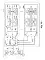
- FIG. 1Ais a block diagram of an apparatus in the form of a computing system including a memory device in accordance with a number of embodiments of the present disclosure.
- a host 110can include a processing resource, such as logic resource 112 .
- a logic resourcealso referred to sometimes as “logic layer” or just “logic” is intended to mean firmware (e.g., in the form of microcode instructions) and/or hardware such as transistor circuitry and/or one or more application specific integrated circuits (ASICs).
- the logic resource 112can include a static random access memory (SRAM) memory on the logic resource 112 .
- SRAMstatic random access memory
- the logic resource 112can be coupled on the host 110 to a cache memory 113 on the host 110 , e.g., on-package (also referred to as on-chip and/or on-die) such as in a 3D integrated memory.
- the logic resource 112can be coupled to the cache memory 113 via a wide, e.g., 256 bit interface, interface 114 .
- This interfacemay include through silicon vias (TSVs) as part of a 3D integrated memory having multiple memory die stacked on a logic die.
- TSVsthrough silicon vias
- the cache memory 113shown associated with the host in FIG. 1A , can have a replica in the form of a plurality of arrays, memory layers, banks, bank sections, subarrays, rows, etc., on a memory device 120 in a number of allocated locations in an array 130 of the memory device 120 .
- all or at least a portion of memory device 120may be substituted as cache memory 113 on package with the logic resource 112 on the host 110 .
- Embodimentsare not so limited.
- a portion of the cache memory 113 , and/or the number of allocated locations in the array 130may serve as a last layer cache (LLC) portion.
- LLClast layer cache
- an LLC having and/or able to operate on subrow select and block select metadatacan control block data alignment and may reduce an overall data size of cache memory, whether in a 3D integrated memory chip or in a separate processing in memory random access memory (PIMRAM) device, e.g., memory device 120 .
- PIMRAMmemory random access memory
- a cache controller 115may use firmware (e.g., microcode instructions) and/or hardware, e.g., an application specific integrated circuit (ASIC).
- firmware and/or hardware used by the cache controller 115is configured to create a block select as metadata to a cache line and to create a subrow select as metadata to the cache line (shown in more detail in FIG. 1B ).
- the block selectenables an offset to the cache line and the subrow select enables multiple sets to a set associative cache.
- the block selectprovides an offset to a page in a dynamic random access memory (DRAM).
- DRAMdynamic random access memory
- the cache controller 115can provide cache lines having the block select and the subrow select metadata to the number of allocated locations in array 130 of memory device 120 to provide a compute enabled cache on memory device 120 .
- memory banksmay have independent TSV paths, e.g., interface 114 on host 110 , into them and may be controlled explicitly by the cache controller 115 .
- Cache blocks having subrow select metadata and block select metadatacan be moved from an SRAM in the logic resource 112 into cache memory in DRAM, e.g., as part of a 3D integrated cache memory 113 on host 110 or to a number of allocated locations in array 130 on a PIMRAM 120 .
- the placement of the cache blockswill be controlled using the subrow select and block select metadata data structures created by the cache controller 115 and added to cache lines.
- a “cache block”is intended to mean an addressable area in memory that is being used in a cache memory function.
- An addressable cache blockmay include one or more addressable cache lines.
- an addressable cache linemay have a bit length that is equivalent to an addressable bit width of a cache block, but a cache block may include more than one addressable cache line.
- a cache blockmay have an addressable bit width that is less than an addressable bit length of the cache line, such as an addressable “chunk” within the cache block as described in more detail below.
- a cache linemay be configured to have a bit length of 128 bytes.
- An addressable cache block on the particular device or on another device, e.g., memory device 120may also have an addressable bit width of 128 bytes.
- block select metadata data structuresaccording to various embodiments are provided that enable a selection of all and/or a portion of that 128 byte bit length to the cache line, e.g., the entire 128 bytes and/or a portion of having a smaller bit length (referred to herein as a “chunk”) of just 256 bits, 64 bits, etc. Embodiments are not so limited.
- the block select and subrow select metadata data structurescreated by the cache controller 115 , are data structures used internal to the compute enabled cache, e.g., stored and maintained between the cache controller 115 and cache memory 113 on the host or between the number of allocated locations in array 130 and a controller 140 on the PIMRAM 120 .
- the subrow select and block select metadata data structuresdo not have to be stored, maintained or tracked as part of an address to the logic resource 112 on the host 110 .
- the cache controller 115 and/or controller 140 on the memory device 120is configured, by firmware and/or hardware executing instructions and/or performing logic operations, to be able to change the block select and the subrow select and to relocate the cache block data transparently to the logic resource 112 on the host 110 .
- the cache controller 115can additionally be configured to store and maintain a copy of the block select and subrow select metadata structures with the logic resource 112 on the host 110 .
- FIG. 1Bis a block diagram illustrating the use of a cache line having a block select and subrow select for storage and/or retrieval of cache blocks in an array.
- the cache controller 115 and/or controller 140 described in FIG. 1Amay be configured, by firmware, and/or hardware executing instructions and/or performing logic operations, to create a block select 162 and row select 163 data structure to insert in a cache line 160 .
- an address 161 including a tag and an offsetmay be provided according to a cache memory architecture of a host 110 or other device, e.g., memory device 120 .
- the received addressmay be compared to a cache line 160 , e.g., compared to direct mapped tags, for one or more matches 165 indicating a location in cache memory, generally shown by arrow 171 , to locate the cache line.
- a controllere.g., cache controller 115 and/or controller 140 , can insert additional block select 162 and row select 163 metadata data structures into the cache line 160 which may be used to specify a particular cache block, 127 - 0 , . . .
- a particular cache blocke.g., block 127 - 5
- a particular rowe.g., row 126 - 0 , row 126 - 1 , etc.
- a particular compute componente.g., 150 - 5
- sensing circuitry 150 of an array/sensing circuitry alignment 130 / 150e.g., according to a particular digit line/compute component alignment as described in more detail in connection with FIGS. 2 and 3 .
- the block select metadata data structure 162may provide an offset to the cache line and function as an offset to a page in DRAM.
- the block select metadata 162may be used to control alignment of cache blocks within an array in the cache memory 113 on the host 110 (shown in FIG. 1A ) or may be used by controller 140 to control alignment of cache blocks within array 130 in the memory device 120 .
- the subrow select metadata 163may enable multiple sets in a set associative cache and may control placement of a cache block such that a replicated and/or split cache line and/or cache block may be placed on multiple different rows in an array in the cache memory 113 on host or array 130 on the memory device 120 .
- set associative cacherefers to combination of direct mapped cache (e.g., in which each block is mapped to exactly one location) and fully associative cache (e.g., which is similar to direct cache mapping but allows a cache block to be mapped to any cache location).
- each cache blockis mapped to a subset of cache locations.
- the term “multiple sets”is intended to mean that the subrow select metadata may allow for a cache line and/or cache block to be split and/or replicated such that the split cache line and/or split block can be placed in multiple different subsets of cache locations in order to achieved a particular alignment.
- the subrow select metadata data structure 163allows for a given cache line to be placed on multiple different rows. As shown in FIG. 1B the subrow select metadata data structure 163 can be added as a portion of a tag.
- a “tag” to a cache lineis intended to mean a unique identifier for a group of data in the cache.
- Metadatais intended to mean one or more additional bits that serve as additional information about the data to which it is associated, e.g., data describing other data.
- FIG. 1Billustrates an example 1K (one Kilobit) cache line 160 including metadata and tags along with cache block data.
- the additional block select metadata 162 and the subrow select metadata 163e.g., as may be created by the cache controller 115 , are inserted (as shown by “arrow”) into the cache line 160 .
- the block select metadata data structure 162 and subrow select metadata data structure 163advantageously contribute to providing a compute enabled cache on a host 110 and/or on a memory device 120 in several ways.
- a DRAMwill access significantly more data than requested.
- a cache request of 256 bitsmay cause a DRAM to access up to 16K+ columns (16,000+ bits). If this 256 cache request were to a cache memory system having a bit width of only 128 bytes, then the cache request of 256 bits would only use power and signaling time to access a row having a bit width of 128 bytes. To cause a DRAM to access a full 16K+ columns (16K+ bits) may be significantly more costly in use of power and signaling time than accessing a row having a bit width of only 128 bytes in a 128 byte cache memory architecture.
- a block select metadata data structure 162can selectively control which part of that same 16+ Kbit wide row of bits to access, e.g., shown by match selection “arrow” 167 .
- arrow 167illustrates the block select metadata 162 being used to select a particular cache block 127 - 0 , . . . , 127 -N, in an array 121 of cache memory (e.g., in cache memory 113 on host 110 or in a number of locations in an array 130 on memory device 120 in FIG. 1A ) to access.
- a cache controller 115may access the metadata data structures (e.g., block select 162 and subrow select 163 ) described herein and operate to compare information therein, e.g., bits (flags), or other value in a multiple bit scenario, to a reference bit or bit value to determine a logical action or subsequent action.
- metadata data structurese.g., block select 162 and subrow select 163
- the array in cache memory 121can be a DRAM bank that is 16 k columns wide. There may be a plurality of bank sections 123 within a DRAM bank to the array 121 and each bank section 123 may have a particular number of rows, e.g., a bank section 123 may have 512 rows.
- FIG. 1Bshows a plurality of blocks 127 - 0 , . . . , 127 -N across a 16K+ column wide bank section 123 .
- the block select metadata 162can be used by a cache controller 115 and/or a controller 140 in a PIM capable device to select which part of an entire 16K+ bit wide row of bits to access, equivalent to a cache line bit length.
- the block select metadata 162may be used to select of all and/or a portion of a 128 byte bit length cache line, e.g., the entire 128 bytes and/or a portion of having a smaller bit length.
- the block select metadata 162may be used to select a smaller bit length, e.g., a 256 bit chunk.
- the purpose for selecting the smaller bit length, e.g., equating to a 256 bit chunk,may be to match a bit width to a particular interface, for example a 256 bit interface ( 114 in FIG. 1A ) to a 16K+ column memory array. This may, for example, provide even further granularity to a 16K+ column wide DRAM row access.
- the block select metadata 162may be six (6) bits wide to select a 256 bit chunk.
- the block select metadata 162 data structuremay be eight (8) bits wide to provide further granularity and to access a 64 bit value within a 256 bit chunk.
- the term “chunk”is intended to refer to a smaller bit length portion of a cache block depending on a particular design implementation.
- a cache blockmay have a bit length of 128 bytes and a “chunk in a particular design implementation may have a smaller, defined bit length, e.g., 256 bits, 64 bits, etc.
- each cache linecan be handled as having one or more vectors and a vector may have a plurality of elements having multiple bits representing numerical values.
- a vectormay have four (4) 64 bit values, e.g., numerical values.
- Each 64 bit valuecan be an element to a vector in a logical operation.
- the vector or the individual elementsmay be handled as a “chunk” as described herein.
- Block select metadata 162may be used to control the alignment of such a “chunk”, e.g., vector and/or the elements to a vector, in an array, subarray, etc.
- the additional subrow select metadata data structure 163may be inserted (as shown by “arrow”) into the cache line 160 and used to select which row, e.g., which row in a subarray, to access.
- the subrow select metadata structure 163can be added to a portion of the tags in the cache line 160 .
- a four (4) bit subrow select data structure 163will allow a selection of one (1) of sixteen (16) rows in a DRAM array, e.g., within a 16 row subarray, for a given cache block 127 - 0 , . . . , 127 -N.
- the subrow select metadata 163is thus shown in the example of FIG. 1B being used to select, e.g., at arrow 169 , a row in a subarray 125 .
- the subrow select metadata 163could also be used to select which subarray a particular element is placed in as a resource allocation.
- FIG. 1Cis a block diagram illustrating that the block select and subrow select data structures to a cache line can be used to separate a cache line 160 into chunks 190 .
- a chunkmay have a smaller bit length than that of an entire cache line or cache block width in a DRAM array, e.g., blocks 127 - 0 , . . . , 127 -N shown in FIG. 1B .
- the different selected bit width to a chunkmay depend on a particular design implementation. In one embodiment a chunk is chosen to have a bit width of 256 bits to match a width of a particular interface bandwidth, e.g., interface 114 in FIG. 1A , also having a bit width of 256 bits.
- the block select (BS) metadata data structure 162may be used as an offset to the cache line 160 to select a particular chunk, e.g., Chunk 0 , in a given cache line 160 .
- the subrow select (SRS) metadata data structure 163may be used to allow for a given cache line 160 to be placed on multiple different rows in a cache block, e.g., cache block 127 - 0 , . . . , 127 -N, in an array, bank, bank section, subarray, etc., as shown in FIG. 1B .
- FIG. 1Cillustrates that the block select metadata data structure 162 and the subrow select metadata data structure 163 can be repeated to allow a cache line to be split and placed differently within a cache block, array, and/or memory device.
- the subrow select metadata data structure 163allows for multiple placements vertically and enables joining data items that may need to be combined, e.g., in a PIM based device.
- addition the two additional metadata data structures, block select and subrow selectcan control the alignment (block select) and resource allocation (subrow select) to provide a compute enabled cache.
- PIMRAMPIM based dynamic random access memory
- FIG. 1Aadditionally shows the coupling of a host 110 to a memory device 120 .
- a cache line with block select 162 and subrow select metadata data structurescan be stored in quickly accessible dynamic random access memory (DRAM) and operated by the controller 140 and/or sensing circuitry 150 to a PIMRAM.
- DRAMdynamic random access memory
- Thisthen affords an efficient method of providing a large number of instructions, with arguments, to the DRAM and then route those instructions to an embedded processing engine, e.g., controller 140 and/or sensing circuitry 150 , of the DRAM with low latency, while preserving the protocol, logical, and electrical interfaces for the DRAM.
- embodiments described hereinmay facilitate keeping the A/C bus at a standard width and data rate, reducing any amount of “special” design for the PIMRAM and also making the PIMRAM more compatible with existing memory interfaces in a variety of computing devices.
- bit vectoris intended to mean a physically contiguous number of bits on a bit vector operation capable memory device, e.g., PIM device, whether physically contiguous in rows (e.g., horizontally oriented) or columns (e.g., vertically oriented) in an array of memory cells.
- bit vector operationis intended to mean an operation that is performed on a bit-vector that is a contiguous portion (also referred to as “chunk”) of virtual address space, e.g., used by a PIM device.
- a chunk of virtual address spacemay have a bit length of 256 bits.
- a chunkmay or may not be contiguous physically to other chunks in the virtual address space.
- bit vectors comprising variable bit-length vectorsmay be divided. This can include dividing a first vector with variable length elements by a second vector with variable length elements.
- the first vectorcan represent a number of dividends and be stored in a group of memory cells coupled to a first access line and a number of sense lines in an array.
- the second vectorcan represent a number of divisors and be stored in a group of memory cells coupled to a second access line and the number of sense lines in the array.
- the division operationcan include a number of AND operations, OR operations, SHIFT operations, and INVERT operations performed without transferring data via an input/output (I/O) line.
- a first element and a second elementcan be numerical values that are divided by each other.
- Elements to be dividedcan be referred to as operands of a division operation.
- the elementscan be numerical values that can be stored in memory as bit-vectors and retrieved to and stored in a last layer cache (LLC), DRAM equivalent in the PIMRAM to be operated upon according to embodiments of the present disclosure.
- LLClast layer cache
- the embodimentscan allow a host system to allocate a number of locations, e.g., sub-arrays (or “subarrays”) or portions of subarrays in a plurality of DRAM banks to cache blocks.
- the host system and/or the PIMRAMmay perform the address resolution for a cache line on an entire cache block, including the addition of the block select metadata data structures 162 and the subrow select metadata data structures 163 .
- the cache lines 160 and cache blocks 127 - 0 , . . . , 127 -Nmay then be written into the allocated instruction locations, e.g., subarrays, within a target bank. Command may utilize the normal DRAM write path to the DRAM device.
- a DRAM bank controllermay retrieve and operate on the cache lines 160 and cache blocks 127 - 0 , . . . , 127 -N in an equivalent manner to a last layer cache's (LLCs) operation on a host, e.g., 110 in FIG. 1A .
- the memory controllerwill pull cache block data from the storage subarrays as necessary to handle the branches, loops, logical and data operations contained with the instruction block, caching the instructions and refilling the LLC cache as necessary.
- PIMDRAM processor-in-memory
- program instructionse.g., PIM commands
- a memory device having PIM capabilitiescan distribute implementation of the PIM commands over multiple sensing circuitries that can implement logical operations and can store the PIM commands within the memory array, e.g., without having to transfer them back and forth with a host over an A/C bus for the memory device.
- PIM commands involving a memory device having PIM capabilitiescan be completed in less time and using less power.
- a number of embodiments of the present disclosurecan provide improved parallelism and/or reduced power consumption in association with performing compute functions as compared to previous systems such as previous PIM systems and systems having an external processor (e.g., a processing resource located external from a memory array, such as on a separate integrated circuit chip).
- a number of embodimentscan provide for performing fully complete compute functions such as integer add, subtract, multiply, divide, and CAM (content addressable memory) functions without transferring data out of the memory array and sensing circuitry via a bus (e.g., data bus, address bus, control bus), for instance.
- Such compute functionscan involve performing a number of logical operations (e.g., logical functions such as AND, OR, NOT, NOR, NAND, XOR, etc.).
- performing logical operationscan include performing a number of non-Boolean logic operations such as copy, compare, destroy, etc.
- datamay be transferred from the array and sensing circuitry (e.g., via a bus comprising input/output (I/O) lines) to a processing resource such as a processor, microprocessor, and/or compute engine, which may comprise ALU circuitry and/or other functional unit circuitry configured to perform the appropriate logical operations.
- a processing resourcesuch as a processor, microprocessor, and/or compute engine, which may comprise ALU circuitry and/or other functional unit circuitry configured to perform the appropriate logical operations.
- transferring data from a memory array and sensing circuitry to such processing resource(s)can involve significant power consumption.
- a sense linewhich may be referred to herein as a digit line or data line
- I/O linese.g., local I/O lines
- the circuitry of the processing resource(s)may not conform to pitch rules associated with a memory array.
- the cells of a memory arraymay have a 4F 2 or 6F 2 cell size, where “F” is a feature size corresponding to the cells.
- the devicese.g., logic gates
- ALU circuitry of previous PIM systemsmay not be capable of being formed on pitch with the memory cells, which can affect chip size and/or memory density, for example.
- a number of embodiments of the present disclosureinclude sensing circuitry formed on pitch with an array of memory cells and capable of performing compute functions such as gather and scatter operations local to the array of memory cells.
- FIGS. 1A and 1Dare block diagrams of an apparatus in the form of a computing system 100 including a memory device 120 in accordance with a number of embodiments of the present disclosure.
- the host 110 , logic 112 , cache memory 113 and cache controllerhave been discussed in detail above.
- the memory device 120 shown in FIG. 1Acan include a controller 140 , e.g., memory controller, a channel controller 143 , a bank arbiter 145 , a high speed interface (HSI) 141 , a memory array 130 having sensing circuitry 150 and/or logic circuitry 170 .
- a controller 140e.g., memory controller, a channel controller 143 , a bank arbiter 145 , a high speed interface (HSI) 141 , a memory array 130 having sensing circuitry 150 and/or logic circuitry 170 .
- HSEhigh speed interface
- FIGS. 1A and 1Dshow the system 100 includes a host 110 coupled (e.g., connected) to the memory device 120 , which includes a memory array 130 .
- Host 110can be a host system such as a personal laptop computer, a desktop computer, a digital camera, a smart phone, or a memory card reader, among various other types of hosts.
- Host 110can include a system motherboard and/or backplane and can include a number of processing resources (e.g., one or more processors, microprocessors, or some other type of controlling circuitry).
- the system 100can include separate integrated circuits or both the host 110 and the memory device 120 can be on the same integrated circuit.
- the system 100can be, for instance, a server system and/or a high performance computing (HPC) system and/or a portion thereof.
- HPChigh performance computing
- FIGS. 1A and 1Dillustrates a system having a Von Neumann architecture
- embodiments of the present disclosurecan be implemented in non-Von Neumann architectures, which may not include one or more components (e.g., CPU, ALU, etc.) often associated with a Von Neumann architecture.
- the memory array 130can be a DRAM array, SRAM array, STT RAM array, PCRAM array, TRAM array, RRAM array, NAND flash array, and/or NOR flash array, for instance.
- the array 130can comprise memory cells arranged in rows coupled by access lines (which may be referred to herein as word lines or select lines) and columns coupled by sense lines, which may be referred to herein as data lines or digit lines. Although a single array 130 is shown in FIG. 1A , embodiments are not so limited.
- memory device 120may include a number of arrays 130 (e.g., a number of banks of DRAM cells, NAND flash cells, etc.).
- the memory device 120includes address circuitry 142 to latch address signals provided over a data bus 156 (e.g., an I/O bus) through I/O circuitry 144 . Status and/or exception information can be provided from the controller 140 on the memory device 120 to a channel controller 143 , including an out-of-band bus 157 , which in turn can be provided from the memory device 120 to the host 110 . Address signals are received through address circuitry 142 and decoded by a row decoder 146 and a column decoder 152 to access the memory array 130 . A number of designated portions of the array 130 may be provided to receive and to store compute enabled cache lines having subrow select metadata data structures 163 and block select metadata data structures 162 .
- Datacan be read from memory array 130 by sensing voltage and/or current changes on the data lines using sensing circuitry 150 .
- the sensing circuitry 150can read and latch a page (e.g., row) of data from the memory array 130 .
- the I/O circuitry 144can be used for bi-directional data communication with host 110 over the data bus 156 .
- the write circuitry 148is used to write data to the memory array 130 .
- Controller 140may decode signals provided by control bus 154 from the host 110 . These signals can include chip enable signals, write enable signals, and address latch signals that are used to control operations performed on the memory array 130 , including data read, data write, and data erase operations. In various embodiments, the controller 140 is responsible for executing instructions from the host 110 .
- the controller 140can be a state machine, a sequencer, or some other type of controller.
- the controller 140can control shifting data (e.g., right or left) in an array, e.g., memory array 130 .
- the sensing circuitry 150can comprise a number of sense amplifiers and a number of compute components, which may serve as, and be referred to herein as, an accumulator and can be used to perform logical operations (e.g., on data associated with complementary data lines).
- the sensing circuitry 150can be used to perform logical operations using data stored in array 130 as inputs and store the results of the logical operations back to the array 130 without transferring data via a sense line address access (e.g., without firing a column decode signal).
- various compute functionscan be performed using, and within, sensing circuitry 150 rather than (or in association with) being performed by processing resources external to the sensing circuitry (e.g., by a processor associated with host 110 and/or other processing circuitry, such as ALU circuitry, located on device 120 (e.g., on controller 140 or elsewhere)).
- sensing circuitry 150is configured to perform logical operations on data stored in memory array 130 and store the result back to the memory array 130 without enabling an I/O line (e.g., a local I/O line) coupled to the sensing circuitry 150 .
- the sensing circuitry 150can be formed on pitch with the memory cells of the array.
- Logic circuitry 170can be coupled to the sensing circuitry 150 and can include additional peripheral sense amplifiers, registers, cache and/or data buffers to store, cache and/or buffer, results of operations described herein.
- circuitry external to array 130 and sensing circuitry 150is not needed to perform compute functions as the sensing circuitry 150 can perform the appropriate logical operations to perform such compute functions without the use of an external processing resource. Therefore, the sensing circuitry 150 may be used to compliment and/or to replace, at least to some extent, such an external processing resource (or at least the bandwidth consumption of such an external processing resource).
- the array 130 and sensing circuitrycan function according to embodiments as a compute enabled cache upon the controller 140 receiving and operating on a cache line 160 having block select 162 and subrow select 163 metadata structures.
- the sensing circuitry 150may be used to perform logical operations (e.g., to execute instructions) in addition to logical operations performed by an external processing resource (e.g., host 110 ).
- host 110 and/or sensing circuitry 150may be limited to performing only certain logical operations and/or a certain number of logical operations.
- Enabling an I/O linecan include enabling (e.g., turning on) a transistor having a gate coupled to a decode signal (e.g., a column decode signal) and a source/drain coupled to the I/O line.
- a decode signale.g., a column decode signal
- embodimentsare not limited to not enabling an I/O line.
- the sensing circuitrye.g., 150
- the local I/O line(s)may be enabled in order to transfer a result to a suitable location other than back to the array 130 (e.g., to an external register).
- FIG. 1Dis a block diagram of another apparatus architecture in the form of a computing system 100 including a plurality of memory devices 120 - 1 , . . . , 120 -N coupled to a host 110 via a channel controller 143 in accordance with a number of embodiments of the present disclosure.
- the channel controller 143may be coupled to the plurality of memory devices 120 - 1 , . . . , 120 -N in an integrated manner in the form of a module 118 , e.g., formed on same chip with the plurality of memory devices 120 - 1 , . . . , 120 -N.
- the channel controller 143may be integrated with the host 110 , as illustrated by dashed lines 111 , e.g., formed on a separate chip from the plurality of memory devices 120 - 1 , . . . , 120 -N.
- the channel controller 143can be coupled to each of the plurality of memory devices 120 - 1 , . . . , 120 -N via a control bus 154 as described in FIG. 1A which in turn can be coupled to the host 110 .
- the channel controller 143can also be coupled to each of the plurality of memory devices, 120 - 1 , . . . , 120 -N via a data bus 156 as described in FIG. 1A which in turn can be coupled to the host 110 .
- channel controller 143can be coupled to each of the plurality of memory devices 120 - 1 , . . . , 120 -N via an out-of-bound (OOB) bus 157 associated with a high speed interface (HSI) 141 that is configured to report status, exception and other data information to the channel controller 143 to exchange with the host 110 .
- OOBout-of-bound
- HSEhigh speed interface
- the channel controller 143can receive the status and exception information from a high speed interface (HSI) (also referred to herein as a status channel interface) 141 associated with a bank arbiter 145 in each of the plurality of memory devices 120 - 1 , . . . , 120 -N.
- HAIhigh speed interface
- each of the plurality of memory devices 120 - 1 , . . . , 120 -Ncan include a bank arbiter 145 to sequence control and data with a plurality of banks, e.g., Bank zero (0), Bank one (1), . . . , Bank six (6), Bank seven (7), etc.
- Each of the plurality of banks, Bank 0 , . . . , Bank 7can include a controller 140 and other components, including an array of memory cells 130 and sensing circuitry 150 , logic circuitry 170 , etc., as described in connection with FIG. 1A .
- each of the plurality of banks, e.g., Bank 0 , . . . , Bank 7 , in the plurality of memory devices 120 - 1 , . . . , 120 -Ncan include address circuitry 142 to latch address signals for data provided over a data bus 156 (e.g., an I/O bus) through I/O circuitry 144 .
- Status and/or exception informationcan be provided from the controller 140 on the memory device 120 to the channel controller 143 , using the OOB bus 157 , which in turn can be provided from the plurality of memory devices 120 - 1 , . . . , 120 -N to the host 110 .
- address signalscan be received through address circuitry 142 and decoded by a row decoder 146 and a column decoder 152 to access the memory array 130 .
- Datacan be read from memory array 130 by sensing voltage and/or current changes on the data lines using sensing circuitry 150 .
- the sensing circuitry 150can read and latch a page (e.g., row) of data from the memory array 130 .
- the I/O circuitry 144can be used for bi-directional data communication with host 110 over the data bus 156 .
- the write circuitry 148is used to write data to the memory array 130 and the 00 B bus 157 can be used to report status, exception and other data information to the channel controller 143 .
- the channel controller 143can include one or more local buffers to store an program instructions and can include logic 160 to allocate a plurality of locations, e.g., subarrays or portions of subarrays, in the arrays of each respective bank to store bank commands, and arguments, (PIM commands) for the various banks associated with to operation of each of the plurality of memory devices 120 - 1 , . . . , 120 -N.
- the channel controller 143can dispatch commands, e.g., PIM commands, to the plurality of memory devices 120 - 1 , . . . , 120 -N to store those program instructions within a given bank of a memory device.
- the memory array 130can be a DRAM array, SRAM array, STT RAM array, PCRAM array, TRAM array, RRAM array, NAND flash array, and/or NOR flash array, for instance.
- the array 130can comprise memory cells arranged in rows coupled by access lines (which may be referred to herein as word lines or select lines) and columns coupled by sense lines, which may be referred to herein as data lines or digit lines.
- a controller 140e.g., bank control logic and/or sequencer, associated with any particular bank, Bank 0 , . . . , Bank 7 , in a given memory device, 120 - 1 , . . . , 120 -N, can decode signals provided by control bus 154 from the host 110 . These signals can include chip enable signals, write enable signals, and address latch signals that are used to control operations performed on the memory array 130 , including data read, data write, and data erase operations.
- the controller 140is responsible for executing instructions from the host 110 .
- the controller 140can be a state machine, a sequencer, or some other type of controller.
- the controller 140can control shifting data (e.g., right or left) in an array, e.g., memory array 130 .
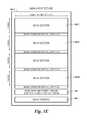
- FIG. 1Eis a block diagram of a bank 121 - 1 to a memory device in accordance with a number of embodiments of the present disclosure. That is bank 121 - 1 can represent an example bank to a memory device such as Bank 0 , . . . , Bank 7 ( 121 - 0 , . . . , 121 - 7 ) shown in FIG. 1B . As described in FIG. 1B , a bank architecture can include a plurality of main memory columns (shown horizontally as X), e.g., 16,384 columns in an example DRAM bank. Additionally, the bank 121 - 1 may be divided up into sections, 123 - 1 , 123 - 2 , . . .
- Each of the bank sections 123 - 1 , . . . , 123 -Ncan include a plurality of rows (shown vertically as Y), e.g., each section may include 16,384 rows in an example DRAM bank.
- One or more of the bank sections 123 - 1 , . . . , 123 -Nmay include a number of locations configured to receive and store compute enabled cache blocks, e.g., 127 - 0 , . . . , 127 -N as shown in FIG. 1B , having subrow select and block select metadata data structures.
- Example embodimentsare not limited to the example horizontal and/or vertical orientation of columns and rows described here or the example numbers thereof.
- the bank architecturecan include logic circuitry 170 , such as sense amplifiers, registers, cache and data buffering, that is coupled to the bank sections 123 - 1 , . . . , 123 -N.
- the logic circuitry 170can provide another form of cache such as logic circuitry 170 associated with the sensing circuitry 150 and array 130 as shown in FIG. 1A .
- the bank architecturecan be associated with bank control, e.g., controller, 140 .
- the bank control shown in FIG. 1Ecan, in example, represent at least a portion of the functionality embodied by and contained in the controller 140 shown in FIGS. 1A and 1D .
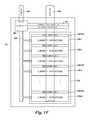
- FIG. 1Fis another block diagram of a bank 121 to a memory device in accordance with a number of embodiments of the present disclosure.
- bank 121can represent an example bank to a memory device such as Bank 0 , . . . , Bank 7 ( 121 - 0 , . . . , 121 - 7 ) shown in FIG. 1D .
- a bank architecturecan include a control bus 154 coupled controller 140 .
- the controller 140 shown in FIG. 1Fcan, for example, represent at least a portion of the functionality embodied by and contained in the controller 140 shown in FIGS. 1 A and 1 D. Also, as shown in FIG.
- the bank architecturecan include a data bus 156 coupled to a plurality of control/data registers in an instruction, e.g., program instructions (PIM commands), read path 151 and coupled to a plurality of bank sections, e.g., bank section 123 , in a particular bank 121 .
- PIM commandsprogram instructions
- a bank section 123can be further subdivided into a plurality of sub-arrays (or subarrays) 125 - 1 , 125 - 2 , . . . , 125 -N again separated by of plurality of sensing circuitry and logic 150 / 170 as shown in FIG. 1A and described further in connection with FIGS. 2-4 .
- a bank section 121may be divided into sixteen (16) subarrays. However, embodiments are not limited to this example number.
- 125 -Nmay include a number of locations configured to receive and store compute enabled cache blocks, e.g., 127 - 0 , . . . , 127 -N as shown in FIG. 1B , having subrow select and block select metadata data structures.
- compute enabled cache blockse.g., 127 - 0 , . . . , 127 -N as shown in FIG. 1B , having subrow select and block select metadata data structures.
- FIG. 1Fillustrates a controller 140 coupled to a write path 149 and coupled to each of the subarrays 125 - 1 , . . . , 125 -N in the bank 123 .
- logic circuitry 170 shown in FIG. 1Amay be used as an instruction cache, e.g., used to cache and/or re-cache retrieved instructions local (“on-pitch”) to a particular bank.
- a plurality of locationsfor storing program instructions, e.g., PIM commands, and/or constant data to a bank 123 in a memory device.
- the controller 140is configured to receive a block of instructions, compute enabled cache blocks, e.g., 127 - 0 , . . . , 127 -N as shown in FIG. 1B having subrow select and block select metadata data structures, and/or constant data from a host, e.g., host 110 in FIG. 1A .
- the block of instructions, compute enabled cache blockse.g., 127 - 0 , . . . , 127 -N as shown in FIG.
- 1B having subrow select and block select metadata data structures, and/or constant datamay be received to the controller 140 from a channel controller 143 either integrated with the host 110 or separate from the host, e.g., integrated in the form of a module 118 with a plurality of memory devices, 120 - 1 , . . . , 120 -N, as shown in FIG. 1D .
- the block of instructions and/or datacan include a set of program instructions, e.g. PIM commands, and/or constant data, e.g., data to set up for PIM calculations.
- the controller 140is configured to store the block of instructions and/or constant data from the host 110 and/or channel controller 143 in an array, e.g., array 130 shown in FIG. 1A and/or 123 shown in FIG. 1D , of a bank, e.g., banks 121 - 0 , . . . , 121 - 7 , shown in FIGS. 1D, 1E and 1F .
- the controller 140is further configured, e.g.
- sensing circuitryincludes logic in the form of hardware circuitry and/or application specific integrated circuitry (ASIC), to route the program instructions to the sensing circuitry, including a compute component, such as sensing circuitry shown as 150 in FIG. 1A and compute components 231 and 331 in FIGS. 2 and 3 , to perform logical functions and/or operations, e.g., program instruction execution, as described herein.
- ASICapplication specific integrated circuitry
- the controller 140is configured to use DRAM protocol and DRAM logical and electrical interfaces to receive the program instructions and/or constant data from the host 110 and/or channel controller 143 and to route the program instructions and/or constant data to a compute component of sensing circuitry 150 , 250 and/or 350 .
- the program instructions and/or constant data received to the controller 140can be pre-resolved, e.g., pre-defined, by a programmer and/or provided to the host 110 and/or channel controller 143 .
- the array of memory cellsincludes a plurality of banks of memory cells 120 - 1 , . . . , 120 -N and the memory device 120 includes a bank arbiter 145 coupled to each of the plurality of banks 120 - 1 , . . . , 120 -N.
- each bank arbiteris configured to receive an instruction block of program instructions, compute enabled cache blocks having subrow select and block select metadata data structures, and/or constant data relevant to a particular bank from the bank arbiter 145 .
- the controller 140can then store instructions in the received instruction block, compute enabled cache blocks, and/or constant data to a plurality of locations for the particular bank as allocated by the host 110 and/or channel controller 143 .
- the host 110 and/or channel controller 143is configured to address translate the plurality of locations for the bank arbiter 145 to assign to banks of the memory device 120 .
- the plurality of locationsincludes a number of subarrays 125 - 1 , . . . , 125 -N in the DRAM banks 121 - 1 , . . . , 121 - 7 and/or portions of the number of subarrays.
- each controller 140can be configured to receive compute enabled cache lines 160 from the host 110 and/or channel controller 143 , e.g., on data bus 156 , to store cache blocks received to a given bank, 121 - 1 , . . . , 121 - 7 .
- the controller 140is configured to then retrieve cache block data on data bus 156 with control and data registers 151 , from the plurality of locations for the particular bank and execute logical operations using the compute component of the sensing circuitry 150 .
- the controller 140can cache retrieved cache blocks local to the particular bank, e.g. array 130 , bank sections 123 and/or subarray 125 , to handle branches, loops, logical and data operations contained within the instructions block execution. And, the controller 140 can re-cache retrieved instructions as needed.
- the size of the dedicated instruction memory (cache) on the DRAM partdoes not have to be increased for a PIM system.
- a plurality of memory devices 120 - 1 , . . . , 120 -Nare coupled to a host 110 and/or channel controller 143 .
- the host 110 and/or channel controller 143can dispatch cache blocks to an appropriate bank arbiter 145 - 1 , . . . , 145 -N for the plurality of memory devices, 120 - 1 , . . . , 120 -N, e.g., over a data bus 156 .
- the controller 140is configured such that a bank 121 can receive a subsequent cache line 160 associated with another cache block relevant to the particular bank and use the block select 162 and subrow select 163 metadata data structures in the received cache lines 160 to store and access cache blocks to/from a plurality of locations for the particular bank while, e.g., in parallel, the controller 140 is operating on another previously retrieved cache block.
- the embodiments described hereinavoid needing to wait for future, or a next set of cache block access instructions, e.g., PIM commands, to be received from a host 110 and/or channel controller 143 .
- the apparatus and methods devices described hereinfacilitate the memory device 120 functioning as a last layer cache (LLC) in a DRAM part for cache blocks and can facilitate a compute enabled cache directly on-chip, on-pitch with the memory device 120 in the PIM system, e.g., PIMRAM.
- LLClast layer cache
- the controller 140is configure to control the execution of program instructions, e.g., PIM commands, by controlling the sensing circuitry 150 , including compute components 251 and/or 351 , to implement logical functions such as AND, OR, NOT, NAND, NOR, and XOR logical functions. Additionally the controller 140 is configured to control the sensing circuitry 150 to perform non-Boolean logic operations, including copy, compare and erase operations, as part of executing program instructions, e.g., PIM commands.
- program instructionse.g., PIM commands
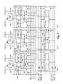
- FIG. 2is a schematic diagram illustrating sensing circuitry 250 in accordance with a number of embodiments of the present disclosure.
- the sensing circuitry 250can correspond to sensing circuitry 150 shown in FIGS. 1A and 1B .
- the sense amplifier 206 of sensing circuitry 250can correspond to sense amplifiers 206 shown in FIG. 2
- the compute component 231 of sensing circuitry 250can correspond to sensing circuitry, including compute component, 150 shown in FIG. 1A , for example.
- a memory cellcomprises a storage element (e.g., capacitor) and an access device (e.g., transistor).
- a first memory cellcomprises transistor 202 - 1 and capacitor 203 - 1
- a second memory cellcomprises transistor 202 - 2 and capacitor 203 - 2
- the memory array 230is a DRAM array of 1T1C (one transistor one capacitor) memory cells.
- the memory cellsmay be destructive read memory cells (e.g., reading the data stored in the cell destroys the data such that the data originally stored in the cell is refreshed after being read).
- the cells of the memory array 230can be arranged in rows coupled by word lines 204 -X (Row X), 204 -Y (Row Y), etc., and columns coupled by pairs of complementary sense lines (e.g., data lines DIGIT(n ⁇ 1)/DIGIT(n ⁇ 1)_, DIGIT(n)/DIGIT(n)_, DIGIT(n+1)/DIGIT(n+1)_).
- the individual sense lines corresponding to each pair of complementary sense linescan also be referred to as data lines 205 - 1 (D) and 205 - 2 (D_) respectively.
- D_data lines 205 - 1 (D) and 205 - 2
- FIG. 2Although only one pair of complementary data lines are shown in FIG. 2 , embodiments of the present disclosure are not so limited, and an array of memory cells can include additional columns of memory cells and/or data lines (e.g., 4,096, 8,192, 16,384, etc.).
- Memory cellscan be coupled to different data lines and/or word lines.
- a first source/drain region of a transistor 202 - 1can be coupled to data line 205 - 1 (D)
- a second source/drain region of transistor 202 - 1can be coupled to capacitor 203 - 1
- a gate of a transistor 202 - 1can be coupled to word line 204 -X.
- a first source/drain region of a transistor 202 - 2can be coupled to data line 205 - 2 (D_)
- a second source/drain region of transistor 202 - 2can be coupled to capacitor 203 - 2
- a gate of a transistor 202 - 2can be coupled to word line 204 -Y.
- the cell plateas shown in FIG. 2 , can be coupled to each of capacitors 203 - 1 and 203 - 2 .
- the cell platecan be a common node to which a reference voltage (e.g., ground) can be applied in various memory array configurations.
- a reference voltagee.g., ground
- the memory array 230is coupled to sensing circuitry 250 in accordance with a number of embodiments of the present disclosure.
- the sensing circuitry 250comprises a sense amplifier 206 and a compute component 231 corresponding to respective columns of memory cells (e.g., coupled to respective pairs of complementary data lines).
- the sense amplifier 206can be coupled to the pair of complementary sense lines 205 - 1 and 205 - 2 .
- the compute component 231can be coupled to the sense amplifier 206 via pass gates 207 - 1 and 207 - 2 .
- the gates of the pass gates 207 - 1 and 207 - 2can be coupled to logical operation selection logic 213 .
- the logical operation selection logic 213can be configured to include pass gate logic for controlling pass gates that couple the pair of complementary sense lines un-transposed between the sense amplifier 206 and the compute component 231 (as shown in FIG. 2 ) and/or swap gate logic for controlling swap gates that couple the pair of complementary sense lines transposed between the sense amplifier 206 and the compute component 231 .
- the logical operation selection logic 213can also be coupled to the pair of complementary sense lines 205 - 1 and 205 - 2 .
- the logical operation selection logic 213can be configured to control continuity of pass gates 207 - 1 and 207 - 2 based on a selected logical operation, as described in detail below for various configurations of the logical operation selection logic 413 .
- the sense amplifier 206can be operated to determine a data value (e.g., logic state) stored in a selected memory cell.
- the sense amplifier 206can comprise a cross coupled latch, which can be referred to herein as a primary latch.
- the circuitry corresponding to sense amplifier 206comprises a latch 215 including four transistors coupled to a pair of complementary data lines D 205 - 1 and D_ 205 - 2 .
- embodimentsare not limited to this example.
- the latch 215can be a cross coupled latch (e.g., gates of a pair of transistors, such as n-channel transistors (e.g., NMOS transistors) 227 - 1 and 227 - 2 are cross coupled with the gates of another pair of transistors, such as p-channel transistors (e.g., PMOS transistors) 229 - 1 and 229 - 2 ).
- the cross coupled latch 215comprising transistors 227 - 1 , 227 - 2 , 229 - 1 , and 229 - 2 can be referred to as a primary latch.
- the voltage on one of the data lines 205 - 1 (D) or 205 - 2 (D_)will be slightly greater than the voltage on the other one of data lines 205 - 1 (D) or 205 - 2 (D_).
- An ACT signal and the RNL* signalcan be driven low to enable (e.g., fire) the sense amplifier 206 .
- the data lines 205 - 1 (D) or 205 - 2 (D_) having the lower voltagewill turn on one of the PMOS transistor 229 - 1 or 229 - 2 to a greater extent than the other of PMOS transistor 229 - 1 or 229 - 2 , thereby driving high the data line 205 - 1 (D) or 205 - 2 (D_) having the higher voltage to a greater extent than the other data line 205 - 1 (D) or 205 - 2 (D_) is driven high.
- the data line 205 - 1 (D) or 205 - 2 (D_) having the higher voltagewill turn on one of the NMOS transistor 227 - 1 or 227 - 2 to a greater extent than the other of the NMOS transistor 227 - 1 or 227 - 2 , thereby driving low the data line 205 - 1 (D) or 205 - 2 (D_) having the lower voltage to a greater extent than the other data line 205 - 1 (D) or 205 - 2 (D_) is driven low.
- the data line 205 - 1 (D) or 205 - 2 (D_) having the slightly greater voltageis driven to the voltage of the supply voltage V CC through source transistor 211 , and the other data line 205 - 1 (D) or 205 - 2 (D_) is driven to the voltage of the reference voltage (e.g., ground) through the sink transistor 213 .
- the reference voltagee.g., ground
- the cross coupled NMOS transistors 227 - 1 and 227 - 2 and PMOS transistors 229 - 1 and 229 - 2serve as a sense amplifier pair, which amplify the differential voltage on the data lines 205 - 1 (D) and 205 - 2 (D_) and operate to latch a data value sensed from the selected memory cell.
- the cross coupled latch of sense amplifier 206may be referred to as a primary latch 215 .
- Embodimentsare not limited to the sense amplifier 206 configuration illustrated in FIG. 2 .
- the sense amplifier 206can be current-mode sense amplifier and/or single-ended sense amplifier (e.g., sense amplifier coupled to one data line).
- embodiments of the present disclosureare not limited to a folded data line architecture such as that shown in FIG. 2 .
- the sense amplifier 206can, in conjunction with the compute component 231 , be operated to perform various logical operations using data from an array as input.
- the result of a logical operationcan be stored back to the array without transferring the data via a data line address access (e.g., without firing a column decode signal such that data is transferred to circuitry external from the array and sensing circuitry via local I/O lines).
- a number of embodiments of the present disclosurecan enable performing logical operations and compute functions associated therewith using less power than various previous approaches.
- a number of embodimentscan enable an increased parallel processing capability as compared to previous approaches.
- the sense amplifier 206can further include equilibration circuitry 214 , which can be configured to equilibrate the data lines 205 - 1 (D) and 205 - 2 (D_).
- the equilibration circuitry 214comprises a transistor 224 coupled between data lines 205 - 1 (D) and 205 - 2 (D_).
- the equilibration circuitry 214also comprises transistors 225 - 1 and 225 - 2 each having a first source/drain region coupled to an equilibration voltage (e.g., V DD /2), where V DD is a supply voltage associated with the array.
- a second source/drain region of transistor 225 - 1can be coupled data line 205 - 1 (D), and a second source/drain region of transistor 225 - 2 can be coupled data line 205 - 2 (D_).
- Gates of transistors 224 , 225 - 1 , and 225 - 2can be coupled together, and to an equilibration (EQ) control signal line 226 .
- activating EQenables the transistors 224 , 225 - 1 , and 225 - 2 , which effectively shorts data lines 205 - 1 (D) and 205 - 2 (D_) together and to the an equilibration voltage (e.g., V CC /2).
- FIG. 2shows sense amplifier 206 comprising the equilibration circuitry 214
- the equilibration circuitry 214may be implemented discretely from the sense amplifier 206 , implemented in a different configuration than that shown in FIG. 2 , or not implemented at all.
- the sensing circuitrye.g., sense amplifier 206 and compute component 231
- the sensing circuitrycan be operated to perform a selected logical operation and initially store the result in one of the sense amplifier 206 or the compute component 231 without transferring data from the sensing circuitry via an I/O line (e.g., without performing a data line address access via activation of a column decode signal, for instance).
- Boolean logic functionsare used in many higher level functions. Consequently, speed and/or power efficiencies that can be realized with improved logical operations, can translate into speed and/or power efficiencies of higher order functionalities.
- the compute component 231can also comprise a latch, which can be referred to herein as a secondary latch 264 .
- the secondary latch 264can be configured and operated in a manner similar to that described above with respect to the primary latch 215 , with the exception that the pair of cross coupled p-channel transistors (e.g., PMOS transistors) comprising the secondary latch can have their respective sources coupled to a supply voltage (e.g., V DD ), and the pair of cross coupled n-channel transistors (e.g., NMOS transistors) of the secondary latch can have their respective sources selectively coupled to a reference voltage (e.g., ground), such that the secondary latch is continuously enabled.
- the configuration of the compute componentis not limited to that shown in FIG. 2 at 231 , and various other embodiments are described further below.
- FIG. 3is a schematic diagram illustrating sensing circuitry capable of implementing an XOR logical operation in accordance with a number of embodiments of the present disclosure.
- FIG. 3shows a sense amplifier 306 coupled to a pair of complementary sense lines 305 - 1 and 305 - 2 , and a compute component 331 coupled to the sense amplifier 306 via pass gates 307 - 1 and 307 - 2 .
- the sense amplifier 306 shown in FIG. 3can correspond to sense amplifier 206 shown in FIG. 2 .
- the compute component 331 shown in FIG. 3can correspond to sensing circuitry, including compute component, 150 shown in FIG. 1A , for example.
- the logical operation selection logic 313 shown in FIG. 3can correspond to logical operation selection logic 413 shown in FIG. 4 , for example.
- the gates of the pass gates 307 - 1 and 307 - 2can be controlled by a logical operation selection logic signal, Pass.
- a logical operation selection logic signalPass.
- an output of the logical operation selection logiccan be coupled to the gates of the pass gates 307 - 1 and 307 - 2 .
- the compute component 331can comprise a loadable shift register configured to shift data values left and right.
- the compute components 331can comprise respective stages (e.g., shift cells) of a loadable shift register configured to shift data values left and right.
- each compute component 331 (e.g., stage) of the shift registercomprises a pair of right-shift transistors 381 and 386 , a pair of left-shift transistors 389 and 390 , and a pair of inverters 387 and 388 .
- the signals PHASE 1 R, PHASE 2 R, PHASE 1 L, and PHASE 2 Lcan be applied to respective control lines 382 , 383 , 391 and 392 to enable/disable feedback on the latches of the corresponding compute components 331 in association with performing logical operations and/or shifting data in accordance with embodiments described herein.
- the sensing circuitry shown in FIG. 3also shows a logical operation selection logic 313 coupled to a number of logic selection control input control lines, including ISO, TF, TT, FT, and FF. Selection of a logical operation from a plurality of logical operations is determined from the condition of logic selection control signals on the logic selection control input control lines, as well as the data values present on the pair of complementary sense lines 305 - 1 and 305 - 2 when the isolation transistors are enabled via the ISO control signal being asserted.
- a logical operation selection logic 313coupled to a number of logic selection control input control lines, including ISO, TF, TT, FT, and FF.
- the logical operation selection logic 313can include four logic selection transistors: logic selection transistor 362 coupled between the gates of the swap transistors 342 and a TF signal control line, logic selection transistor 352 coupled between the gates of the pass gates 307 - 1 and 307 - 2 and a TT signal control line, logic selection transistor 354 coupled between the gates of the pass gates 307 - 1 and 307 - 2 and a FT signal control line, and logic selection transistor 364 coupled between the gates of the swap transistors 342 and a FF signal control line.
- Gates of logic selection transistors 362 and 352are coupled to the true sense line through isolation transistor 350 - 1 (having a gate coupled to an ISO signal control line).
- Gates of logic selection transistors 364 and 354are coupled to the complementary sense line through isolation transistor 350 - 2 (also having a gate coupled to an ISO signal control line).
- Data values present on the pair of complementary sense lines 305 - 1 and 305 - 2can be loaded into the compute component 331 via the pass gates 307 - 1 and 307 - 2 .
- the compute component 331can comprise a loadable shift register.
- the pass gates 307 - 1 and 307 - 2are OPEN, data values on the pair of complementary sense lines 305 - 1 and 305 - 2 are passed to the compute component 331 and thereby loaded into the loadable shift register.
- the data values on the pair of complementary sense lines 305 - 1 and 305 - 2can be the data value stored in the sense amplifier 306 when the sense amplifier is fired.
- the logical operation selection logic signal, Passis high to OPEN the pass gates 307 - 1 and 307 - 2 .
- the ISO, TF, TT, FT, and FF control signalscan operate to select a logical function to implement based on the data value (“B”) in the sense amplifier 306 and the data value (“A”) in the compute component 331 .
- the ISO, TF, TT, FT, and FF control signalsare configured to select the logical function to implement independent from the data value present on the pair of complementary sense lines 305 - 1 and 305 - 2 (although the result of the implemented logical operation can be dependent on the data value present on the pair of complementary sense lines 305 - 1 and 305 - 2 .
- the ISO, TF, TT, FT, and FF control signalsselect the logical operation to implement directly since the data value present on the pair of complementary sense lines 305 - 1 and 305 - 2 is not passed through logic to operate the gates of the pass gates 307 - 1 and 307 - 2 .
- FIG. 3shows swap transistors 342 configured to swap the orientation of the pair of complementary sense lines 305 - 1 and 305 - 2 between the sense amplifier 313 - 7 and the compute component 331 .
- the swap transistors 342are OPEN, data values on the pair of complementary sense lines 305 - 1 and 305 - 2 on the sense amplifier 306 side of the swap transistors 342 are oppositely-coupled to the pair of complementary sense lines 305 - 1 and 305 - 2 on the compute component 331 side of the swap transistors 342 , and thereby loaded into the loadable shift register of the compute component 331 .
- the logical operation selection logic signal Passcan be activated (e.g., high) to OPEN the pass gates 307 - 1 and 307 - 2 (e.g., conducting) when the ISO control signal line is activated and either the TT control signal is activated (e.g., high) with data value on the true sense line is “1” or the FT control signal is activated (e.g., high) with the data value on the complement sense line is “1.”
- the data value on the true sense linebeing a “1” OPENs logic selection transistors 352 and 362 .
- the data value on the complimentary sense linebeing a “1” OPENs logic selection transistors 354 and 364 . If the ISO control signal or either the respective TT/FT control signal or the data value on the corresponding sense line (e.g., sense line to which the gate of the particular logic selection transistor is coupled) is not high, then the pass gates 307 - 1 and 307 - 2 will not be OPENed by a particular logic selection transistor.
- the logical operation selection logic signal PassFcan be activated (e.g., high) to OPEN the swap transistors 342 (e.g., conducting) when the ISO control signal line is activated and either the TF control signal is activated (e.g., high) with data value on the true sense line is “1,” or the FF control signal is activated (e.g., high) with the data value on the complement sense line is “1.” If either the respective control signal or the data value on the corresponding sense line (e.g., sense line to which the gate of the particular logic selection transistor is coupled) is not high, then the swap transistors 342 will not be OPENed by a particular logic selection transistor.
- the Pass* control signalis not necessarily complementary to the Pass control signal. It is possible for the Pass and Pass* control signals to both be activated or both be deactivated at the same time. However, activation of both the Pass and Pass* control signals at the same time shorts the pair of complementary sense lines together, which may be a disruptive configuration to be avoided.
- the sensing circuitry illustrated in FIG. 3is configured to select one of a plurality of logical operations to implement directly from the four logic selection control signals (e.g., logical operation selection is not dependent on the data value present on the pair of complementary sense lines). Some combinations of the logic selection control signals can cause both the pass gates 307 - 1 and 307 - 2 and swap transistors 342 to be OPEN at the same time, which shorts the pair of complementary sense lines 305 - 1 and 305 - 2 together.
- the logical operations which can be implemented by the sensing circuitry illustrated in FIG. 3can be the logical operations summarized in the logic tables shown in FIG. 4 .
- FIG. 4is a logic table illustrating selectable logic operation results implemented by a sensing circuitry shown in FIG. 3 in accordance with a number of embodiments of the present disclosure.
- the four logic selection control signalse.g., TF, TT, FT, and FF
- the four control signalsin conjunction with a particular data value present on the complementary sense lines, can be used to select one of plural logical operations to implement involving the starting data values stored in the sense amplifier 306 and compute component 331 .
- the four control signalsin conjunction with a particular data value present on the complementary sense lines, controls the continuity of the pass gates 307 - 1 and 307 - 2 and swap transistors 342 , which in turn affects the data value in the compute component 331 and/or sense amplifier 306 before/after firing.
- the capability to selectably control continuity of the swap transistors 342facilitates implementing logical operations involving inverse data values (e.g., inverse operands and/or inverse result), among others.
- Logic Table 4 - 1 illustrated in FIG. 4shows the starting data value stored in the compute component 331 shown in column A at 444 , and the starting data value stored in the sense amplifier 306 shown in column B at 445 .
- the other 3 column headings in Logic Table 4 - 1refer to the continuity of the pass gates 307 - 1 and 307 - 2 , and the swap transistors 342 , which can respectively be controlled to be OPEN or CLOSED depending on the state of the four logic selection control signals (e.g., TF, TT, FT, and FF), in conjunction with a particular data value present on the pair of complementary sense lines 305 - 1 and 305 - 2 .
- logic selection control signalse.g., TF, TT, FT, and FF
- the “Not Open” columncorresponds to the pass gates 307 - 1 and 307 - 2 and the swap transistors 342 both being in a non-conducting condition
- the “Open True”corresponds to the pass gates 307 - 1 and 307 - 2 being in a conducting condition
- the “Open Invert”corresponds to the swap transistors 342 being in a conducting condition.
- the configuration corresponding to the pass gates 307 - 1 and 307 - 2 and the swap transistors 342 both being in a conducting conditionis not reflected in Logic Table 4 - 1 since this results in the sense lines being shorted together.
- the nine different selectable logical operations that can be implemented by the sensing circuitrye.g., 150 in FIG. 1A
- Logic Table 4 - 2 illustrated in FIG. 4including an XOR logical operation.
- the columns of Logic Table 4 - 2 illustrated in FIG. 4show a heading 480 that includes the state of logic selection control signals.
- the state of a first logic selection control signalis provided in row 476
- the state of a second logic selection control signalis provided in row 477
- the state of a third logic selection control signalis provided in row 478
- the state of a fourth logic selection control signalis provided in row 479 .
- the particular logical operation corresponding to the resultsis summarized in row 447 .
- sensing circuitrysense amplifiers
- compute componentdynamic latches
- isolation devicesisolation devices
- shift circuitryshift circuitry
Landscapes
- Engineering & Computer Science (AREA)
- Theoretical Computer Science (AREA)
- Physics & Mathematics (AREA)
- General Engineering & Computer Science (AREA)
- General Physics & Mathematics (AREA)
- Software Systems (AREA)
- Microelectronics & Electronic Packaging (AREA)
- Computer Hardware Design (AREA)
- Mathematical Physics (AREA)
- Databases & Information Systems (AREA)
- Memory System Of A Hierarchy Structure (AREA)
Abstract
Description
Claims (44)
Priority Applications (10)
| Application Number | Priority Date | Filing Date | Title |
|---|---|---|---|
| US15/066,488US10073786B2 (en) | 2015-05-28 | 2016-03-10 | Apparatuses and methods for compute enabled cache |
| EP16800515.5AEP3304319B1 (en) | 2015-05-28 | 2016-05-19 | Apparatuses and methods for compute enabled cache |
| CN201680030869.8ACN107683505B (en) | 2015-05-28 | 2016-05-19 | Apparatus and method for compute-enabled cache |
| PCT/US2016/033259WO2016191191A1 (en) | 2015-05-28 | 2016-05-19 | Apparatuses and methods for compute enabled cache |
| TW105116507ATWI651617B (en) | 2015-05-28 | 2016-05-26 | Apparatuses and methods for compute enabled cache |
| US16/126,169US10372612B2 (en) | 2015-05-28 | 2018-09-10 | Apparatuses and methods for compute enabled cache |
| US16/531,619US10970218B2 (en) | 2015-05-28 | 2019-08-05 | Apparatuses and methods for compute enabled cache |
| US17/222,642US11599475B2 (en) | 2015-05-28 | 2021-04-05 | Apparatuses and methods for compute enabled cache |
| US18/117,974US12050536B2 (en) | 2015-05-28 | 2023-03-06 | Apparatuses and methods for compute enabled cache |
| US18/759,068US20240354254A1 (en) | 2015-05-28 | 2024-06-28 | Apparatuses and methods for compute enabled cache |
Applications Claiming Priority (2)
| Application Number | Priority Date | Filing Date | Title |
|---|---|---|---|
| US201562167451P | 2015-05-28 | 2015-05-28 | |
| US15/066,488US10073786B2 (en) | 2015-05-28 | 2016-03-10 | Apparatuses and methods for compute enabled cache |
Related Child Applications (1)
| Application Number | Title | Priority Date | Filing Date |
|---|---|---|---|
| US16/126,169ContinuationUS10372612B2 (en) | 2015-05-28 | 2018-09-10 | Apparatuses and methods for compute enabled cache |
Publications (2)
| Publication Number | Publication Date |
|---|---|
| US20160350230A1 US20160350230A1 (en) | 2016-12-01 |
| US10073786B2true US10073786B2 (en) | 2018-09-11 |
Family
ID=57394277
Family Applications (6)
| Application Number | Title | Priority Date | Filing Date |
|---|---|---|---|
| US15/066,488Active2036-08-17US10073786B2 (en) | 2015-05-28 | 2016-03-10 | Apparatuses and methods for compute enabled cache |
| US16/126,169ActiveUS10372612B2 (en) | 2015-05-28 | 2018-09-10 | Apparatuses and methods for compute enabled cache |
| US16/531,619ActiveUS10970218B2 (en) | 2015-05-28 | 2019-08-05 | Apparatuses and methods for compute enabled cache |
| US17/222,642Active2036-04-22US11599475B2 (en) | 2015-05-28 | 2021-04-05 | Apparatuses and methods for compute enabled cache |
| US18/117,974ActiveUS12050536B2 (en) | 2015-05-28 | 2023-03-06 | Apparatuses and methods for compute enabled cache |
| US18/759,068PendingUS20240354254A1 (en) | 2015-05-28 | 2024-06-28 | Apparatuses and methods for compute enabled cache |
Family Applications After (5)
| Application Number | Title | Priority Date | Filing Date |
|---|---|---|---|
| US16/126,169ActiveUS10372612B2 (en) | 2015-05-28 | 2018-09-10 | Apparatuses and methods for compute enabled cache |
| US16/531,619ActiveUS10970218B2 (en) | 2015-05-28 | 2019-08-05 | Apparatuses and methods for compute enabled cache |
| US17/222,642Active2036-04-22US11599475B2 (en) | 2015-05-28 | 2021-04-05 | Apparatuses and methods for compute enabled cache |
| US18/117,974ActiveUS12050536B2 (en) | 2015-05-28 | 2023-03-06 | Apparatuses and methods for compute enabled cache |
| US18/759,068PendingUS20240354254A1 (en) | 2015-05-28 | 2024-06-28 | Apparatuses and methods for compute enabled cache |
Country Status (5)
| Country | Link |
|---|---|
| US (6) | US10073786B2 (en) |
| EP (1) | EP3304319B1 (en) |
| CN (1) | CN107683505B (en) |
| TW (1) | TWI651617B (en) |
| WO (1) | WO2016191191A1 (en) |
Families Citing this family (60)
| Publication number | Priority date | Publication date | Assignee | Title |
|---|---|---|---|---|
| US9430191B2 (en)* | 2013-11-08 | 2016-08-30 | Micron Technology, Inc. | Division operations for memory |
| US10223309B2 (en)* | 2014-12-19 | 2019-03-05 | Rambus Inc. | Dynamic random access memory (DRAM) component for high-performance, high-capacity registered memory modules |
| US10073786B2 (en)* | 2015-05-28 | 2018-09-11 | Micron Technology, Inc. | Apparatuses and methods for compute enabled cache |
| US10235176B2 (en) | 2015-12-17 | 2019-03-19 | The Charles Stark Draper Laboratory, Inc. | Techniques for metadata processing |
| US9997232B2 (en)* | 2016-03-10 | 2018-06-12 | Micron Technology, Inc. | Processing in memory (PIM) capable memory device having sensing circuitry performing logic operations |
| US11386010B2 (en) | 2016-09-27 | 2022-07-12 | Integrated Silicon Solution, (Cayman) Inc. | Circuit engine for managing memory meta-stability |
| US11010294B2 (en) | 2016-09-27 | 2021-05-18 | Spin Memory, Inc. | MRAM noise mitigation for write operations with simultaneous background operations |
| US10991410B2 (en)* | 2016-09-27 | 2021-04-27 | Spin Memory, Inc. | Bi-polar write scheme |
| US10990465B2 (en) | 2016-09-27 | 2021-04-27 | Spin Memory, Inc. | MRAM noise mitigation for background operations by delaying verify timing |
| US10818331B2 (en) | 2016-09-27 | 2020-10-27 | Spin Memory, Inc. | Multi-chip module for MRAM devices with levels of dynamic redundancy registers |
| US11119910B2 (en) | 2016-09-27 | 2021-09-14 | Spin Memory, Inc. | Heuristics for selecting subsegments for entry in and entry out operations in an error cache system with coarse and fine grain segments |
| US11048633B2 (en) | 2016-09-27 | 2021-06-29 | Spin Memory, Inc. | Determining an inactive memory bank during an idle memory cycle to prevent error cache overflow |
| US11151042B2 (en) | 2016-09-27 | 2021-10-19 | Integrated Silicon Solution, (Cayman) Inc. | Error cache segmentation for power reduction |
| US11119936B2 (en) | 2016-09-27 | 2021-09-14 | Spin Memory, Inc. | Error cache system with coarse and fine segments for power optimization |
| WO2018090255A1 (en)* | 2016-11-16 | 2018-05-24 | 华为技术有限公司 | Memory access technique |
| US20180191862A1 (en)* | 2016-12-29 | 2018-07-05 | Microsoft Technology Licensing, Llc | Detection and delegation of action tasks |
| US10162756B2 (en)* | 2017-01-18 | 2018-12-25 | Intel Corporation | Memory-efficient last level cache architecture |
| US10403352B2 (en)* | 2017-02-22 | 2019-09-03 | Micron Technology, Inc. | Apparatuses and methods for compute in data path |
| US10185674B2 (en) | 2017-03-22 | 2019-01-22 | Micron Technology, Inc. | Apparatus and methods for in data path compute operations |
| US10049721B1 (en) | 2017-03-27 | 2018-08-14 | Micron Technology, Inc. | Apparatuses and methods for in-memory operations |
| US9997212B1 (en) | 2017-04-24 | 2018-06-12 | Micron Technology, Inc. | Accessing data in memory |
| US10942843B2 (en)* | 2017-04-25 | 2021-03-09 | Micron Technology, Inc. | Storing data elements of different lengths in respective adjacent rows or columns according to memory shapes |
| US10236038B2 (en) | 2017-05-15 | 2019-03-19 | Micron Technology, Inc. | Bank to bank data transfer |
| US10013197B1 (en) | 2017-06-01 | 2018-07-03 | Micron Technology, Inc. | Shift skip |
| US10262701B2 (en) | 2017-06-07 | 2019-04-16 | Micron Technology, Inc. | Data transfer between subarrays in memory |
| US10416927B2 (en) | 2017-08-31 | 2019-09-17 | Micron Technology, Inc. | Processing in memory |
| US10614875B2 (en) | 2018-01-30 | 2020-04-07 | Micron Technology, Inc. | Logical operations using memory cells |
| US10437557B2 (en) | 2018-01-31 | 2019-10-08 | Micron Technology, Inc. | Determination of a match between data values stored by several arrays |
| US11194477B2 (en) | 2018-01-31 | 2021-12-07 | Micron Technology, Inc. | Determination of a match between data values stored by three or more arrays |
| KR20200116970A (en) | 2018-02-02 | 2020-10-13 | 도버 마이크로시스템즈, 인크. | System and method for converting instructions for metadata processing |
| US20210042100A1 (en) | 2018-02-02 | 2021-02-11 | Dover Microsystems, Inc. | System and method for translating mapping policy into code |
| WO2019152772A1 (en) | 2018-02-02 | 2019-08-08 | The Charles Stark Draper Laboratory, Inc. | Systems and methods for policy execution processing |
| WO2019168752A1 (en)* | 2018-02-27 | 2019-09-06 | Micron Technology, Inc | Three dimensional memory devices |
| US10725696B2 (en) | 2018-04-12 | 2020-07-28 | Micron Technology, Inc. | Command selection policy with read priority |
| WO2019213061A1 (en) | 2018-04-30 | 2019-11-07 | Dover Microsystems, Inc. | Systems and methods for checking safety properties |
| US10440341B1 (en) | 2018-06-07 | 2019-10-08 | Micron Technology, Inc. | Image processor formed in an array of memory cells |
| US11175915B2 (en) | 2018-10-10 | 2021-11-16 | Micron Technology, Inc. | Vector registers implemented in memory |
| US10769071B2 (en) | 2018-10-10 | 2020-09-08 | Micron Technology, Inc. | Coherent memory access |
| US10483978B1 (en) | 2018-10-16 | 2019-11-19 | Micron Technology, Inc. | Memory device processing |
| TW202022679A (en) | 2018-11-06 | 2020-06-16 | 美商多佛微系統公司 | Systems and methods for stalling host processor |
| EP3881190A1 (en) | 2018-11-12 | 2021-09-22 | Dover Microsystems, Inc. | Systems and methods for metadata encoding |
| US11184446B2 (en) | 2018-12-05 | 2021-11-23 | Micron Technology, Inc. | Methods and apparatus for incentivizing participation in fog networks |
| US11841956B2 (en) | 2018-12-18 | 2023-12-12 | Dover Microsystems, Inc. | Systems and methods for data lifecycle protection |
| US11360704B2 (en)* | 2018-12-21 | 2022-06-14 | Micron Technology, Inc. | Multiplexed signal development in a memory device |
| US12393677B2 (en) | 2019-01-18 | 2025-08-19 | Dover Microsystems, Inc. | Systems and methods for metadata classification |
| WO2020167496A1 (en)* | 2019-02-13 | 2020-08-20 | Spin Memory, Inc. | Multi-chip module for mram devices |
| US12118056B2 (en) | 2019-05-03 | 2024-10-15 | Micron Technology, Inc. | Methods and apparatus for performing matrix transformations within a memory array |
| US10867655B1 (en) | 2019-07-08 | 2020-12-15 | Micron Technology, Inc. | Methods and apparatus for dynamically adjusting performance of partitioned memory |
| US11360768B2 (en) | 2019-08-14 | 2022-06-14 | Micron Technolgy, Inc. | Bit string operations in memory |
| WO2021076871A1 (en) | 2019-10-18 | 2021-04-22 | Dover Microsystems, Inc. | Systems and methods for updating metadata |
| US11449577B2 (en) | 2019-11-20 | 2022-09-20 | Micron Technology, Inc. | Methods and apparatus for performing video processing matrix operations within a memory array |
| US11853385B2 (en) | 2019-12-05 | 2023-12-26 | Micron Technology, Inc. | Methods and apparatus for performing diversity matrix operations within a memory array |
| WO2021178493A1 (en) | 2020-03-03 | 2021-09-10 | Dover Microsystems, Inc. | Systems and methods for caching metadata |
| JP7423367B2 (en)* | 2020-03-23 | 2024-01-29 | キオクシア株式会社 | Communication systems, devices, and communication methods |
| CN114158284B (en)* | 2020-07-07 | 2025-07-04 | 北京苹芯科技有限公司 | Apparatus and method for matrix multiplication using in-memory processing |
| US11227641B1 (en) | 2020-07-21 | 2022-01-18 | Micron Technology, Inc. | Arithmetic operations in memory |
| US12124576B2 (en) | 2020-12-23 | 2024-10-22 | Dover Microsystems, Inc. | Systems and methods for policy violation processing |
| US11698853B2 (en)* | 2020-12-31 | 2023-07-11 | Micron Technology, Inc. | Saturating local cache in memory-compute systems |
| CN119252304A (en)* | 2021-04-07 | 2025-01-03 | 华为技术有限公司 | Storage device and method for processing data |
| US20240256448A1 (en)* | 2023-01-31 | 2024-08-01 | Micron Technology, Inc. | Sense amplifiers as static random access memory cache |
Citations (275)
| Publication number | Priority date | Publication date | Assignee | Title |
|---|---|---|---|---|
| US4380046A (en) | 1979-05-21 | 1983-04-12 | Nasa | Massively parallel processor computer |
| US4435793A (en) | 1979-07-26 | 1984-03-06 | Tokyo Shibaura Denki Kabushiki Kaisha | Semiconductor memory device with dummy word line/sense amplifier activation |
| US4435792A (en) | 1982-06-30 | 1984-03-06 | Sun Microsystems, Inc. | Raster memory manipulation apparatus |
| EP0214718A2 (en) | 1985-07-22 | 1987-03-18 | Alliant Computer Systems Corporation | Digital computer |
| US4727474A (en) | 1983-02-18 | 1988-02-23 | Loral Corporation | Staging memory for massively parallel processor |
| US4843264A (en) | 1987-11-25 | 1989-06-27 | Visic, Inc. | Dynamic sense amplifier for CMOS static RAM |
| US4958378A (en) | 1989-04-26 | 1990-09-18 | Sun Microsystems, Inc. | Method and apparatus for detecting changes in raster data |
| US4977542A (en) | 1988-08-30 | 1990-12-11 | Mitsubishi Denki Kabushiki Kaisha | Dynamic semiconductor memory device of a twisted bit line system having improved reliability of readout |
| US5023838A (en) | 1988-12-02 | 1991-06-11 | Ncr Corporation | Random access memory device with integral logic capability |
| US5034636A (en) | 1990-06-04 | 1991-07-23 | Motorola, Inc. | Sense amplifier with an integral logic function |
| US5201039A (en) | 1987-09-30 | 1993-04-06 | Mitsubishi Denki Kabushiki Kaisha | Multiple address-space data processor with addressable register and context switching |
| US5210850A (en) | 1990-06-15 | 1993-05-11 | Compaq Computer Corporation | Memory address space determination using programmable limit registers with single-ended comparators |
| US5253308A (en) | 1989-06-21 | 1993-10-12 | Amber Engineering, Inc. | Massively parallel digital image data processor using pixel-mapped input/output and relative indexed addressing |
| US5276643A (en) | 1988-08-11 | 1994-01-04 | Siemens Aktiengesellschaft | Integrated semiconductor circuit |
| US5325519A (en) | 1991-10-18 | 1994-06-28 | Texas Microsystems, Inc. | Fault tolerant computer with archival rollback capabilities |
| US5367488A (en) | 1992-03-18 | 1994-11-22 | Goldstar Electron Co., Ltd. | DRAM having bidirectional global bit lines |
| US5379257A (en) | 1990-11-16 | 1995-01-03 | Mitsubishi Denki Kabushiki Kaisha | Semiconductor integrated circuit device having a memory and an operational unit integrated therein |
| US5386379A (en) | 1992-01-03 | 1995-01-31 | France Telecom, Establissement Autonome De Droit Public | Memory cell for associative memory |
| US5398213A (en) | 1992-10-08 | 1995-03-14 | Samsung Electronics Co., Ltd. | Access time speed-up circuit for a semiconductor memory device |
| US5440482A (en) | 1993-03-25 | 1995-08-08 | Taligent, Inc. | Forward and reverse Boyer-Moore string searching of multilingual text having a defined collation order |
| US5446690A (en) | 1993-08-10 | 1995-08-29 | Hitachi, Ltd. | Semiconductor nonvolatile memory device |
| US5473576A (en) | 1993-07-27 | 1995-12-05 | Nec Corporation | Dynamic random access memory device with low-power consumption column selector |
| US5481500A (en) | 1994-07-22 | 1996-01-02 | International Business Machines Corporation | Precharged bit decoder and sense amplifier with integrated latch usable in pipelined memories |
| US5485373A (en) | 1993-03-25 | 1996-01-16 | Taligent, Inc. | Language-sensitive text searching system with modified Boyer-Moore process |
| JPH0831168A (en) | 1994-07-13 | 1996-02-02 | Hitachi Ltd | Semiconductor memory device |
| US5506811A (en) | 1993-04-20 | 1996-04-09 | Micron Technology Inc. | Dynamic memory with isolated digit lines |
| US5615404A (en) | 1994-10-31 | 1997-03-25 | Intel Corporation | System having independently addressable bus interfaces coupled to serially connected multi-ported signal distributors generating and maintaining frame based polling schedule favoring isochronous peripherals |
| US5638317A (en) | 1990-08-22 | 1997-06-10 | Texas Instruments Incorporated | Hierarchical DRAM array with grouped I/O lines and high speed sensing circuit |
| US5638128A (en) | 1994-11-08 | 1997-06-10 | General Instrument Corporation Of Delaware | Pixel interpolation filters for video decompression processor |
| US5654936A (en) | 1995-05-25 | 1997-08-05 | Samsung Electronics Co., Ltd. | Control circuit and method for controlling a data line switching circuit in a semiconductor memory device |
| US5678021A (en) | 1992-08-25 | 1997-10-14 | Texas Instruments Incorporated | Apparatus and method for a memory unit with a processor integrated therein |
| US5724366A (en) | 1995-05-16 | 1998-03-03 | Mitsubishi Denki Kabushiki Kaisha | Semiconductor memory device |
| US5724291A (en) | 1995-11-30 | 1998-03-03 | Nec Corporation | Semiconductor memory device with reduced chip area |
| US5751987A (en) | 1990-03-16 | 1998-05-12 | Texas Instruments Incorporated | Distributed processing memory chip with embedded logic having both data memory and broadcast memory |
| US5787458A (en) | 1995-08-31 | 1998-07-28 | Nec Corporation | Content addressable memory of a simple construction capable of retrieving a variable word length data |
| US5854636A (en) | 1994-04-11 | 1998-12-29 | Hitachi, Ltd. | Semiconductor IC with a plurality of processing circuits which receive parallel data via a parallel data transfer circuit |
| US5867429A (en) | 1997-11-19 | 1999-02-02 | Sandisk Corporation | High density non-volatile flash memory without adverse effects of electric field coupling between adjacent floating gates |
| US5870504A (en) | 1996-02-29 | 1999-02-09 | International Business Machines Corporation | High speed outline smoothing method and apparatus including the operation of shifting bits of the current, preceding, and succeeding lines left and right |
| US5915084A (en) | 1996-09-30 | 1999-06-22 | Advanced Micro Devices, Inc. | Scannable sense amplifier circuit |
| US5935263A (en) | 1997-07-01 | 1999-08-10 | Micron Technology, Inc. | Method and apparatus for memory array compressed data testing |
| US5986942A (en) | 1998-01-20 | 1999-11-16 | Nec Corporation | Semiconductor memory device |
| US5991209A (en) | 1997-04-11 | 1999-11-23 | Raytheon Company | Split sense amplifier and staging buffer for wide memory architecture |
| US5991785A (en) | 1997-11-13 | 1999-11-23 | Lucent Technologies Inc. | Determining an extremum value and its index in an array using a dual-accumulation processor |
| US6005799A (en) | 1998-08-06 | 1999-12-21 | Silicon Aquarius | Methods and circuits for single-memory dynamic cell multivalue data storage |
| US6009020A (en) | 1998-03-13 | 1999-12-28 | Nec Corporation | Semiconductor memory device having dynamic data amplifier circuit capable of reducing power dissipation |
| US6092186A (en) | 1996-05-07 | 2000-07-18 | Lucent Technologies Inc. | Apparatus and method for aborting un-needed instruction fetches in a digital microprocessor device |
| US6122211A (en) | 1993-04-20 | 2000-09-19 | Micron Technology, Inc. | Fast, low power, write scheme for memory circuits using pulsed off isolation device |
| US6125071A (en) | 1998-04-22 | 2000-09-26 | Kabushiki Kaisha Toshiba | Semiconductor memory device with high data read rate |
| US6134164A (en) | 1999-04-22 | 2000-10-17 | International Business Machines Corp. | Sensing circuit for a memory cell array |
| US6147514A (en) | 1997-12-11 | 2000-11-14 | Kabushiki Kaisha Toshiba | Sense amplifier circuit |
| US6151244A (en) | 1998-03-17 | 2000-11-21 | Mitsubishi Denki Kabushiki Kaisha | Dynamic semiconductor memory device |
| US6157578A (en) | 1999-07-15 | 2000-12-05 | Stmicroelectronics, Inc. | Method and apparatus for accessing a memory device |
| US6163862A (en) | 1997-12-01 | 2000-12-19 | International Business Machines Corporation | On-chip test circuit for evaluating an on-chip signal using an external test signal |
| US6166942A (en) | 1998-08-21 | 2000-12-26 | Micron Technology, Inc. | Embedded DRAM architecture with local data drivers and programmable number of data read and data write lines |
| US6172918B1 (en) | 1998-12-08 | 2001-01-09 | Mitsubishi Denki Kabushiki Kaisha | Semiconductor memory device allowing high-speed operation of internal data buses |
| US6175514B1 (en) | 1999-01-15 | 2001-01-16 | Fast-Chip, Inc. | Content addressable memory device |
| US6181698B1 (en) | 1997-07-09 | 2001-01-30 | Yoichi Hariguchi | Network routing table using content addressable memory |
| US6208544B1 (en) | 1999-09-09 | 2001-03-27 | Harris Corporation | Content addressable memory cell providing simultaneous read and compare capability |
| US6226215B1 (en) | 1998-12-30 | 2001-05-01 | Hyundai Electronics Industries Co., Ltd. | Semiconductor memory device having reduced data access time and improve speed |
| US20010007112A1 (en) | 1997-07-02 | 2001-07-05 | Porterfield A. Kent | System for implementing a graphic address remapping table as a virtual register file in system memory |
| US20010008492A1 (en) | 2000-01-18 | 2001-07-19 | Fujitsu Limited | Semiconductor memory and method for controlling the same |
| US20010010057A1 (en) | 1997-06-24 | 2001-07-26 | Matsushita Electronics Corporation | Semiconductor integrated circuit, computer system, data processor and data processing method |
| WO2001065359A2 (en) | 2000-02-29 | 2001-09-07 | Peter Petrov | Method and apparatus for building a memory image |
| US6301153B1 (en) | 1997-04-30 | 2001-10-09 | Kabushiki Kaisha Toshiba | Nonvolatile semiconductor memory device |
| US6301164B1 (en) | 2000-08-25 | 2001-10-09 | Micron Technology, Inc. | Antifuse method to repair columns in a prefetched output memory architecture |
| US20010028584A1 (en) | 2000-03-28 | 2001-10-11 | Kabushiki Kaisha Toshiba | Semiconductor memory device having replacing defective columns with redundant columns |
| US6304477B1 (en) | 2001-01-31 | 2001-10-16 | Motorola, Inc. | Content addressable magnetic random access memory |
| US20010043089A1 (en) | 1999-05-26 | 2001-11-22 | Leonard Forbes | Dram sense amplifier for low voltages |
| US6389507B1 (en) | 1999-01-15 | 2002-05-14 | Gigabus, Inc. | Memory device search system and method |
| US20020059355A1 (en) | 1995-08-31 | 2002-05-16 | Intel Corporation | Method and apparatus for performing multiply-add operations on packed data |
| US6418498B1 (en) | 1999-12-30 | 2002-07-09 | Intel Corporation | Integrated system management memory for system management interrupt handler independent of BIOS and operating system |
| US6466499B1 (en) | 2000-07-11 | 2002-10-15 | Micron Technology, Inc. | DRAM sense amplifier having pre-charged transistor body nodes |
| US6510098B1 (en) | 1997-05-28 | 2003-01-21 | Cirrus Logic, Inc. | Method and apparatus for transferring data in a dual port memory |
| US6563754B1 (en) | 2001-02-08 | 2003-05-13 | Integrated Device Technology, Inc. | DRAM circuit with separate refresh memory |
| US6578058B1 (en) | 1999-10-06 | 2003-06-10 | Agilent Technologies, Inc. | System and method for comparing values from target systems |
| US20030167426A1 (en) | 2001-12-20 | 2003-09-04 | Richard Slobodnik | Method and apparatus for memory self testing |
| US20030222879A1 (en) | 2002-04-09 | 2003-12-04 | University Of Rochester | Multiplier-based processor-in-memory architectures for image and graphics processing |
| US20040073592A1 (en) | 2002-06-10 | 2004-04-15 | International Business Machines Corporation | Sense-amp based adder with source follower evaluation tree |
| US20040073773A1 (en) | 2002-02-06 | 2004-04-15 | Victor Demjanenko | Vector processor architecture and methods performed therein |
| US6731542B1 (en) | 2002-12-05 | 2004-05-04 | Advanced Micro Devices, Inc. | Circuit for accurate memory read operations |
| US20040085840A1 (en) | 2001-08-29 | 2004-05-06 | Micron Technology, Inc. | High voltage low power sensing device for flash memory |
| US20040095826A1 (en) | 2002-11-19 | 2004-05-20 | Frederick Perner | System and method for sensing memory cells of an array of memory cells |
| US6754746B1 (en) | 1994-07-05 | 2004-06-22 | Monolithic System Technology, Inc. | Memory array with read/write methods |
| US6768679B1 (en) | 2003-02-10 | 2004-07-27 | Advanced Micro Devices, Inc. | Selection circuit for accurate memory read operations |
| US20040154002A1 (en) | 2003-02-04 | 2004-08-05 | Ball Michael S. | System & method of linking separately compiled simulations |
| US20040205289A1 (en) | 2003-04-11 | 2004-10-14 | Sujaya Srinivasan | Reclaiming blocks in a block-alterable memory |
| US6807614B2 (en) | 2001-07-19 | 2004-10-19 | Shine C. Chung | Method and apparatus for using smart memories in computing |
| US6816422B2 (en) | 2002-05-13 | 2004-11-09 | Renesas Technology Corp. | Semiconductor memory device having multi-bit testing function |
| US6819612B1 (en) | 2003-03-13 | 2004-11-16 | Advanced Micro Devices, Inc. | Apparatus and method for a sense amplifier circuit that samples and holds a reference voltage |
| US20040240251A1 (en) | 2003-05-27 | 2004-12-02 | Rohm Co., Ltd. | Memory device with function to perform operation, and method of performing operation and storage |
| US20050015557A1 (en) | 2002-12-27 | 2005-01-20 | Chih-Hung Wang | Nonvolatile memory unit with specific cache |
| US20050078514A1 (en) | 2003-09-30 | 2005-04-14 | Scheuerlein Roy E. | Multiple twin cell non-volatile memory array and logic block structure and method therefor |
| US20050097417A1 (en) | 2003-11-04 | 2005-05-05 | Agrawal Ghasi R. | Novel bisr mode to test the redundant elements and regular functional memory to avoid test escapes |
| US6894549B2 (en) | 2001-02-21 | 2005-05-17 | Ramtron International Corporation | Ferroelectric non-volatile logic elements |
| US6943579B1 (en) | 2002-12-20 | 2005-09-13 | Altera Corporation | Variable fixed multipliers using memory blocks |
| US6948056B1 (en) | 2000-09-28 | 2005-09-20 | Intel Corporation | Maintaining even and odd array pointers to extreme values by searching and comparing multiple elements concurrently where a pointer is adjusted after processing to account for a number of pipeline stages |
| US6950898B2 (en) | 2000-08-31 | 2005-09-27 | Micron Technology, Inc. | Data amplifier having reduced data lines and/or higher data rates |
| US6950771B1 (en) | 2003-12-09 | 2005-09-27 | Xilinx, Inc. | Correlation of electrical test data with physical defect data |
| US20050223173A1 (en) | 2004-03-31 | 2005-10-06 | Nec Corporation | Set associative cache system and control method for cache memories |
| US6956770B2 (en) | 2003-09-17 | 2005-10-18 | Sandisk Corporation | Non-volatile memory and method with bit line compensation dependent on neighboring operating modes |
| US6961272B2 (en) | 2002-02-15 | 2005-11-01 | Micron Technology, Inc. | Physically alternating sense amplifier activation |
| US6965648B1 (en) | 2000-05-04 | 2005-11-15 | Sun Microsystems, Inc. | Source synchronous link integrity validation |
| US6985394B2 (en) | 2002-12-05 | 2006-01-10 | Samsung Electronics Co., Ltd | Integrated circuit devices including input/output line pairs and precharge circuits and related memory devices |
| US6987693B2 (en) | 2002-09-24 | 2006-01-17 | Sandisk Corporation | Non-volatile memory and method with reduced neighboring field errors |
| US20060047937A1 (en) | 2004-08-30 | 2006-03-02 | Ati Technologies Inc. | SIMD processor and addressing method |
| US7020017B2 (en) | 2004-04-06 | 2006-03-28 | Sandisk Corporation | Variable programming of non-volatile memory |
| US20060069849A1 (en) | 2004-09-30 | 2006-03-30 | Rudelic John C | Methods and apparatus to update information in a memory |
| US7028170B2 (en) | 2000-03-08 | 2006-04-11 | Sun Microsystems, Inc. | Processing architecture having a compare capability |
| US7045834B2 (en) | 1997-08-22 | 2006-05-16 | Micron Technology, Inc. | Memory cell arrays |
| US7054178B1 (en) | 2002-09-06 | 2006-05-30 | Etron Technology, Inc. | Datapath architecture for high area efficiency |
| US7061817B2 (en) | 2004-06-30 | 2006-06-13 | Micron Technology, Inc. | Data path having grounded precharge operation and test compression capability |
| US7073026B2 (en) | 2002-11-26 | 2006-07-04 | Advanced Micro Devices, Inc. | Microprocessor including cache memory supporting multiple accesses per cycle |
| US20060149804A1 (en) | 2004-11-30 | 2006-07-06 | International Business Machines Corporation | Multiply-sum dot product instruction with mask and splat |
| US20060146623A1 (en) | 2000-02-04 | 2006-07-06 | Renesas Technology Corp. | Semiconductor device |
| US7079407B1 (en) | 2002-10-18 | 2006-07-18 | Netlogic Microsystems, Inc. | Content addressable memory (CAM) device including match line sensing |
| US20060181917A1 (en) | 2005-01-28 | 2006-08-17 | Kang Hee-Bok | Semiconductor memory device for low voltage |
| US20060215432A1 (en) | 2005-03-28 | 2006-09-28 | Wickeraad John A | TCAM BIST with redundancy |
| US20060225072A1 (en) | 2004-05-18 | 2006-10-05 | Oracle International Corporation | Packaging multiple groups of read-only files of an application's components into multiple shared libraries |
| US20060291282A1 (en) | 2004-05-07 | 2006-12-28 | Zhizheng Liu | Flash memory cell and methods for programming and erasing |
| US7173857B2 (en) | 2002-05-23 | 2007-02-06 | Renesas Technology Corp. | Nonvolatile semiconductor memory device capable of uniformly inputting/outputting data |
| US7187585B2 (en) | 2005-04-05 | 2007-03-06 | Sandisk Corporation | Read operation for non-volatile storage that includes compensation for coupling |
| US7196928B2 (en) | 2005-04-05 | 2007-03-27 | Sandisk Corporation | Compensating for coupling during read operations of non-volatile memory |
| US20070168615A1 (en) | 2003-03-06 | 2007-07-19 | Koninklijke Philips Electronics N.V. | Data processing system with cache optimised for processing dataflow applications |
| US20070171747A1 (en) | 2006-01-23 | 2007-07-26 | Freescale Semiconductor, Inc. | Memory and method for sensing data in a memory using complementary sensing scheme |
| US20070180006A1 (en) | 2006-01-31 | 2007-08-02 | Renesas Technology Corp. | Parallel operational processing device |
| US20070180184A1 (en) | 2005-12-13 | 2007-08-02 | Mototada Sakashita | Semiconductor device and control method therefor |
| US7260565B2 (en) | 2000-03-09 | 2007-08-21 | Broadcom Corporation | Method and apparatus for high speed table search |
| US7260672B2 (en) | 2001-09-07 | 2007-08-21 | Intel Corporation | Using data stored in a destructive-read memory |
| US20070195602A1 (en) | 2004-12-23 | 2007-08-23 | Yupin Fong | Reducing floating gate to floating gate coupling effect |
| US20070204128A1 (en) | 2003-09-10 | 2007-08-30 | Super Talent Electronics Inc. | Two-Level RAM Lookup Table for Block and Page Allocation and Wear-Leveling in Limited-Write Flash-Memories |
| US20070285131A1 (en) | 2006-04-28 | 2007-12-13 | Young-Soo Sohn | Sense amplifier circuit and sense amplifier-based flip-flop having the same |
| US20070285979A1 (en) | 2004-03-10 | 2007-12-13 | Altera Corporation | Dynamic ram storage techniques |
| US20070291532A1 (en) | 2004-02-23 | 2007-12-20 | Renesas Technology Corp. | Semiconductor integrated circuit device and magnetic memory device capable of maintaining data integrity |
| US20080025073A1 (en) | 2006-07-14 | 2008-01-31 | Igor Arsovski | Self-Referenced Match-Line Sense Amplifier For Content Addressable Memories |
| US20080037333A1 (en) | 2006-04-17 | 2008-02-14 | Kyoung Ho Kim | Memory device with separate read and write gate voltage controls |
| US20080052711A1 (en) | 1998-09-09 | 2008-02-28 | Microsoft Corporation | Highly componentized system architecture with loadable virtual memory manager |
| US7372715B2 (en) | 2006-06-14 | 2008-05-13 | Micron Technology, Inc. | Architecture and method for NAND flash memory |
| US20080137388A1 (en) | 2006-12-08 | 2008-06-12 | Krishnan Rengarajan S | Novel match mismatch emulation scheme for an addressed location in a cam |
| US20080165601A1 (en) | 2007-01-05 | 2008-07-10 | International Business Machines Corporation | eDRAM HIERARCHICAL DIFFERENTIAL SENSE AMP |
| US7400532B2 (en) | 2006-02-16 | 2008-07-15 | Micron Technology, Inc. | Programming method to reduce gate coupling interference for non-volatile memory |
| US20080178053A1 (en) | 2004-01-29 | 2008-07-24 | Gorman Kevin W | Hybrid built-in self test (bist) architecture for embedded memory arrays and an associated method |
| US7406494B2 (en) | 2002-05-14 | 2008-07-29 | Texas Instruments Incorporated | Method of generating a cycle-efficient bit-reverse index array for a wireless communication system |
| US20080209133A1 (en)* | 2007-02-22 | 2008-08-28 | Arm Limited | Managing cache coherency in a data processing apparatus |
| US20080215937A1 (en) | 2004-01-29 | 2008-09-04 | International Business Machines Corporation | Remote bist for high speed test and redundancy calculation |
| US7447720B2 (en) | 2003-04-23 | 2008-11-04 | Micron Technology, Inc. | Method for finding global extrema of a set of bytes distributed across an array of parallel processing elements |
| US7454451B2 (en) | 2003-04-23 | 2008-11-18 | Micron Technology, Inc. | Method for finding local extrema of a set of values for a parallel processing element |
| US7457181B2 (en) | 2005-11-17 | 2008-11-25 | Samsung Electronics Co., Ltd. | Memory device and method of operating the same |
| EP2026209A2 (en) | 2007-08-14 | 2009-02-18 | Dell Products, L.P. | System and method for using a memory mapping function to map memory defects |
| US20090067218A1 (en) | 2007-09-06 | 2009-03-12 | Philippe Graber | Sense amplifier circuitry for integrated circuit having memory cell array, and method of operating same |
| US20090122610A1 (en)* | 2007-11-14 | 2009-05-14 | Kobi Danon | Operation of a non-volatile memory array |
| US7535769B2 (en) | 2005-06-20 | 2009-05-19 | Sandisk Corporation | Time-dependent compensation currents in non-volatile memory read operations |
| US7546438B2 (en) | 2001-07-19 | 2009-06-09 | Chung Shine C | Algorithm mapping, specialized instructions and architecture features for smart memory computing |
| US20090154273A1 (en) | 2007-12-17 | 2009-06-18 | Stmicroelectronics Sa | Memory including a performance test circuit |
| US20090154238A1 (en) | 2007-07-25 | 2009-06-18 | Micron Technology, Inc. | Programming multilevel cell memory arrays |
| US7562198B2 (en) | 2004-06-09 | 2009-07-14 | Renesas Technology Corp. | Semiconductor device and semiconductor signal processing apparatus |
| US7574466B2 (en) | 2003-04-23 | 2009-08-11 | Micron Technology, Inc. | Method for finding global extrema of a set of shorts distributed across an array of parallel processing elements |
| US20090254697A1 (en) | 2008-04-02 | 2009-10-08 | Zikbit Ltd. | Memory with embedded associative section for computations |
| US7602647B2 (en) | 2006-07-20 | 2009-10-13 | Sandisk Corporation | System that compensates for coupling based on sensing a neighbor using coupling |
| JP2009259193A (en) | 2008-02-20 | 2009-11-05 | Renesas Technology Corp | Semiconductor signal processor |
| US7663928B2 (en) | 2007-10-09 | 2010-02-16 | Ememory Technology Inc. | Sense amplifier circuit having current mirror architecture |
| US20100067296A1 (en) | 2006-07-20 | 2010-03-18 | Yan Li | Compensating for coupling during programming |
| US7685365B2 (en) | 2004-09-30 | 2010-03-23 | Intel Corporation | Transactional memory execution utilizing virtual memory |
| US7692466B2 (en) | 2006-08-18 | 2010-04-06 | Ati Technologies Ulc | Sense amplifier based flip-flop |
| US20100091582A1 (en) | 2008-10-09 | 2010-04-15 | Micron Technology, Inc. | Architecture and method for memory programming |
| US7752417B2 (en) | 2006-06-05 | 2010-07-06 | Oracle America, Inc. | Dynamic selection of memory virtualization techniques |
| US20100172190A1 (en) | 2007-09-18 | 2010-07-08 | Zikbit, Inc. | Processor Arrays Made of Standard Memory Cells |
| WO2010079451A1 (en) | 2009-01-08 | 2010-07-15 | Zikbit Ltd. | Memory with smaller, faster, and/or less complex storage cells |
| US20100210076A1 (en) | 2003-04-29 | 2010-08-19 | Infineon Technologies Ag | Memory circuit arrangement and method for the production thereof |
| US20100226183A1 (en) | 2007-03-07 | 2010-09-09 | Mosaid Technologies Incorporated | Partial block erase architecture for flash memory |
| US7796453B2 (en) | 2007-06-29 | 2010-09-14 | Elpida Memory, Inc. | Semiconductor device |
| US7805587B1 (en) | 2006-11-01 | 2010-09-28 | Nvidia Corporation | Memory addressing controlled by PTE fields |
| US7808854B2 (en) | 2008-02-19 | 2010-10-05 | Kabushiki Kaisha Toshiba | Systems and methods for data transfers between memory cells |
| US7827372B2 (en) | 2003-09-04 | 2010-11-02 | Nxp B.V. | Intergrated circuit and a method of cache remapping |
| KR20100134235A (en) | 2009-06-15 | 2010-12-23 | 삼성전자주식회사 | Semiconductor memory device |
| US20100332895A1 (en) | 2009-06-30 | 2010-12-30 | Gurkirat Billing | Non-volatile memory to store memory remap information |
| US7869273B2 (en) | 2007-09-04 | 2011-01-11 | Sandisk Corporation | Reducing the impact of interference during programming |
| US7898864B2 (en) | 2009-06-24 | 2011-03-01 | Sandisk Corporation | Read operation for memory with compensation for coupling based on write-erase cycles |
| US20110051523A1 (en) | 2009-09-02 | 2011-03-03 | Micron Technology, Inc. | Small unit internal verify read in a memory device |
| US20110063919A1 (en) | 2009-09-14 | 2011-03-17 | Micron Technology, Inc. | Memory kink checking |
| US20110093662A1 (en) | 2009-10-21 | 2011-04-21 | Micron Technology, Inc. | Memory having internal processors and data communication methods in memory |
| US20110103151A1 (en) | 2009-11-03 | 2011-05-05 | Samsung Electronics Co., Ltd. | Methods of Programming Semiconductor Memory Devices |
| US20110119467A1 (en) | 2009-11-13 | 2011-05-19 | Nec Laboratories America, Inc. | Massively parallel, smart memory based accelerator |
| US20110122695A1 (en) | 2009-11-24 | 2011-05-26 | Yan Li | Programming memory with bit line floating to reduce channel-to-floating gate coupling |
| US7957206B2 (en) | 2008-04-04 | 2011-06-07 | Micron Technology, Inc. | Read circuitry for an integrated circuit having memory cells and/or a memory cell array, and method of operating same |
| US20110140741A1 (en) | 1999-10-19 | 2011-06-16 | Zerbe Jared L | Integrating receiver with precharge circuitry |
| US7979667B2 (en) | 2007-12-10 | 2011-07-12 | Spansion Llc | Memory array search engine |
| CN102141905A (en) | 2010-01-29 | 2011-08-03 | 上海芯豪微电子有限公司 | Processor system structure |
| US7996749B2 (en) | 2007-07-03 | 2011-08-09 | Altera Corporation | Signal loss detector for high-speed serial interface of a programmable logic device |
| US20110219260A1 (en) | 2007-01-22 | 2011-09-08 | Micron Technology, Inc. | Defective memory block remapping method and system, and memory device and processor-based system using same |
| US8042082B2 (en) | 2007-09-12 | 2011-10-18 | Neal Solomon | Three dimensional memory in a system on a chip |
| US8045391B2 (en) | 2007-06-07 | 2011-10-25 | Sandisk Technologies Inc. | Non-volatile memory and method with improved sensing having bit-line lockout control |
| US20110267883A1 (en) | 2010-05-03 | 2011-11-03 | Peter Wung Lee | Dram-like nvm memory array and sense amplifier design for high temperature and high endurance operation |
| US8059438B2 (en) | 2009-08-28 | 2011-11-15 | International Business Machines Corporation | Content addressable memory array programmed to perform logic operations |
| US20110317496A1 (en) | 2010-06-23 | 2011-12-29 | International Business Machines Corporation | Jam latch for latching memory array output data |
| US20120005397A1 (en) | 2010-07-02 | 2012-01-05 | Hynix Semiconductor Inc. | Sense amplifier and semiconductor apparatus including the same |
| US8095825B2 (en) | 2006-01-16 | 2012-01-10 | Renesas Electronics Corporation | Error correction method with instruction level rollback |
| US20120017039A1 (en) | 2010-07-16 | 2012-01-19 | Plx Technology, Inc. | Caching using virtual memory |
| US20120023281A1 (en) | 1993-09-17 | 2012-01-26 | Shumpei Kawasaki | Single-chip microcomputer |
| US8117462B2 (en) | 2000-08-21 | 2012-02-14 | United States Postal Service | Delivery point validation system |
| US8164942B2 (en) | 2010-02-01 | 2012-04-24 | International Business Machines Corporation | High performance eDRAM sense amplifier |
| US20120120705A1 (en) | 2010-11-11 | 2012-05-17 | Elpida Memory, Inc. | Semiconductor device having bit lines and local i/o lines |
| US20120134216A1 (en) | 2006-06-26 | 2012-05-31 | Micron Technology, Inc. | Integrated circuit having memory array including ecc and column redundancy, and method of operating same |
| US20120134226A1 (en) | 2010-11-29 | 2012-05-31 | Chow Daniel C | Sense amplifier and sense amplifier latch having common control |
| US20120135225A1 (en) | 2009-08-18 | 2012-05-31 | Andre Colas | Multi-layer Transdermal Patch |
| US20120140540A1 (en) | 2009-07-16 | 2012-06-07 | Agam Oren | Charge sharing in a tcam array |
| US8213248B2 (en) | 2009-03-06 | 2012-07-03 | Samsung Electronics Co., Ltd. | Semiconductor memory device having improved local input/output line precharge scheme |
| US8223568B2 (en) | 2008-12-19 | 2012-07-17 | Samsung Electronics Co., Ltd. | Semiconductor memory device adopting improved local input/output line precharging scheme |
| US20120182798A1 (en) | 2000-03-08 | 2012-07-19 | Kabushiki Kaisha Toshiba | Non-Volatile Semiconductor Memory |
| US20120195146A1 (en) | 2011-02-01 | 2012-08-02 | Jun In-Woo | Local sense amplifier circuit and semiconductor memory device including the same |
| US20120198310A1 (en) | 2010-09-28 | 2012-08-02 | Texas Instruments Incorporated | Configurable source based/requestor based error detection and correction for soft errors in multi-level cache memory to minimize cpu interrupt service routines |
| US8238173B2 (en) | 2009-07-16 | 2012-08-07 | Zikbit Ltd | Using storage cells to perform computation |
| US20120246380A1 (en) | 2009-10-21 | 2012-09-27 | Avidan Akerib | Neighborhood operations for parallel processing |
| US8279683B2 (en) | 2004-07-15 | 2012-10-02 | Micron Technology, Inc. | Digit line comparison circuits |
| US8291168B2 (en) | 2008-09-30 | 2012-10-16 | Intel Corporation | Disabling cache portions during low voltage operations |
| US20120265964A1 (en) | 2011-02-22 | 2012-10-18 | Renesas Electronics Corporation | Data processing device and data processing method thereof |
| US20120281486A1 (en) | 2008-08-18 | 2012-11-08 | Elpida Memory, Inc | Semiconductor memory device and method with auxiliary i/o line assist circuit and functionality |
| US8310884B2 (en) | 2009-08-06 | 2012-11-13 | Kabushiki Kaisha Toshiba | Semiconductor memory device |
| US20120303627A1 (en) | 2011-05-23 | 2012-11-29 | Kimberly Keeton | Responding to a query in a data processing system |
| US8332367B2 (en) | 2010-10-20 | 2012-12-11 | International Business Machines Corporation | Parallel data redundancy removal |
| US8339824B2 (en) | 2008-07-02 | 2012-12-25 | Cooke Laurence H | Nearest neighbor serial content addressable memory |
| US8339883B2 (en) | 2009-11-18 | 2012-12-25 | Samsung Electronics Co., Ltd. | Semiconductor memory device |
| US8347154B2 (en) | 2010-09-21 | 2013-01-01 | International Business Machines Corporation | Use of hashing function to distinguish random and repeat errors in a memory system |
| US8351292B2 (en) | 2010-01-15 | 2013-01-08 | Elpida Memory, Inc. | Semiconductor device and data processing system |
| US8356144B2 (en) | 2005-02-10 | 2013-01-15 | Richard Hessel | Vector processor system |
| US20130061006A1 (en) | 2011-09-01 | 2013-03-07 | Elpida Memory, Inc. | Data mask encoding in data bit inversion scheme |
| US8417921B2 (en) | 2008-08-15 | 2013-04-09 | Apple Inc. | Running-min and running-max instructions for processing vectors using a base value from a key element of an input vector |
| WO2013062596A1 (en) | 2011-10-28 | 2013-05-02 | Hewlett-Packard Development Company, L.P. | Row shifting shiftable memory |
| US20130107623A1 (en) | 2011-11-01 | 2013-05-02 | Micron Technology, Inc. | Memory cell sensing |
| US20130117541A1 (en) | 2011-11-04 | 2013-05-09 | Jack Hilaire Choquette | Speculative execution and rollback |
| KR20130049421A (en) | 2011-11-04 | 2013-05-14 | 에스케이하이닉스 주식회사 | Semiconductor memory apparatus and test circuit therefor |
| US20130124783A1 (en) | 2011-11-14 | 2013-05-16 | Samsung Electronics Co., Ltd. | Method of operating nonvolatile memory devices storing randomized data generated by copyback operation |
| US20130132702A1 (en) | 2011-11-22 | 2013-05-23 | Mips Technologies, Inc. | Processor with Kernel Mode Access to User Space Virtual Addresses |
| US20130138646A1 (en) | 2010-04-27 | 2013-05-30 | Emin Gun Sirer | System and methods for mapping and searching objects in multidimensional space |
| US20130138892A1 (en) | 2011-11-30 | 2013-05-30 | Gabriel H. Loh | Dram cache with tags and data jointly stored in physical rows |
| WO2013081588A1 (en) | 2011-11-30 | 2013-06-06 | Intel Corporation | Instruction and logic to provide vector horizontal compare functionality |
| US8462532B1 (en) | 2010-08-31 | 2013-06-11 | Netlogic Microsystems, Inc. | Fast quaternary content addressable memory cell |
| US20130163362A1 (en) | 2011-12-22 | 2013-06-27 | SK Hynix Inc. | Precharge circuit and non-volatile memory device |
| WO2013095592A1 (en) | 2011-12-22 | 2013-06-27 | Intel Corporation | Apparatus and method for vector compute and accumulate |
| US20130173888A1 (en) | 1998-08-24 | 2013-07-04 | Microunity Systems Engineering, Inc. | Processor for Executing Wide Operand Operations Using a Control Register and a Results Register |
| US8484276B2 (en) | 2009-03-18 | 2013-07-09 | International Business Machines Corporation | Processing array data on SIMD multi-core processor architectures |
| US8495438B2 (en) | 2007-12-28 | 2013-07-23 | Texas Instruments Incorporated | Technique for memory imprint reliability improvement |
| US8503250B2 (en) | 2000-07-07 | 2013-08-06 | Mosaid Technologies Incorporated | High speed DRAM architecture with uniform access latency |
| US20130205114A1 (en) | 2006-12-06 | 2013-08-08 | Fusion-Io | Object-based memory storage |
| US20130219112A1 (en) | 2007-10-19 | 2013-08-22 | Virident Systems Inc. | Managing memory systems containing components with asymmetric characteristics |
| US20130227361A1 (en) | 2009-06-30 | 2013-08-29 | Micro Technology, Inc. | Hardwired remapped memory |
| US8526239B2 (en) | 2010-04-29 | 2013-09-03 | Hynix Semiconductor Inc. | Semiconductor memory device and method of operating the same |
| US8533245B1 (en) | 2010-03-03 | 2013-09-10 | Altera Corporation | Multipliers with a reduced number of memory blocks |
| US8555037B2 (en) | 2008-08-15 | 2013-10-08 | Apple Inc. | Processing vectors using wrapping minima and maxima instructions in the macroscalar architecture |
| US20130268711A1 (en) | 2011-11-29 | 2013-10-10 | Robert J. Safranek | Raw memory transaction support |
| US20130283122A1 (en) | 2009-10-15 | 2013-10-24 | Apple Inc. | Error Correction Coding Over Multiple Memory Pages |
| US20130290607A1 (en) | 2012-04-30 | 2013-10-31 | Jichuan Chang | Storing cache metadata separately from integrated circuit containing cache controller |
| US20130286705A1 (en) | 2012-04-26 | 2013-10-31 | David B. Grover | Low power content addressable memory hitline precharge and sensing circuit |
| US8599613B2 (en) | 2011-03-29 | 2013-12-03 | Kabushiki Kaisha Toshiba | Nonvolatile semiconductor memory |
| US20130326154A1 (en) | 2012-05-31 | 2013-12-05 | Samsung Electronics Co., Ltd. | Cache system optimized for cache miss detection |
| US8605015B2 (en) | 2009-12-23 | 2013-12-10 | Syndiant, Inc. | Spatial light modulator with masking-comparators |
| US20130332707A1 (en) | 2012-06-07 | 2013-12-12 | Intel Corporation | Speed up big-number multiplication using single instruction multiple data (simd) architectures |
| US8625376B2 (en) | 2010-11-02 | 2014-01-07 | Hynix Semiconductor Inc. | Semiconductor memory device and method of operation the same |
| US20140032845A1 (en) | 2012-07-30 | 2014-01-30 | Soft Machines, Inc. | Systems and methods for supporting a plurality of load accesses of a cache in a single cycle |
| US8650232B2 (en) | 2009-10-26 | 2014-02-11 | Via Technologies, Inc. | System and method for determination of a horizontal minimum of digital values |
| US20140185395A1 (en) | 2013-01-03 | 2014-07-03 | Seong-young Seo | Methods of copying a page in a memory device and methods of managing pages in a memory system |
| US20140215185A1 (en) | 2013-01-29 | 2014-07-31 | Atmel Norway | Fetching instructions of a loop routine |
| US20140250279A1 (en) | 2013-03-04 | 2014-09-04 | Micron Technology, Inc. | Apparatuses and methods for performing logical operations using sensing circuitry |
| US20140344934A1 (en) | 2013-05-17 | 2014-11-20 | Hewlett-Packard Development Company, L.P. | Bloom filter with memory element |
| US20150033096A1 (en)* | 2011-08-12 | 2015-01-29 | Micron Technology, Inc. | Memory devices and configuration methods for a memory device |
| US20150029798A1 (en) | 2013-07-26 | 2015-01-29 | Micron Technology, Inc. | Apparatuses and methods for performing compare operations using sensing circuitry |
| US20150042380A1 (en) | 2013-08-08 | 2015-02-12 | Micron Technology, Inc. | Apparatuses and methods for performing logical operations using sensing circuitry |
| US20150063052A1 (en) | 2013-08-30 | 2015-03-05 | Micron Technology, Inc. | Independently addressable memory array address spaces |
| US20150078108A1 (en) | 2013-09-19 | 2015-03-19 | Micron Technology, Inc. | Data shifting via a number of isolation devices |
| US9015390B2 (en) | 2003-04-25 | 2015-04-21 | Micron Technology, Inc. | Active memory data compression system and method |
| US20150120987A1 (en) | 2013-10-31 | 2015-04-30 | Micron Technology, Inc. | Apparatuses and methods for identifying an extremum value stored in an array of memory cells |
| US20150134713A1 (en) | 2013-11-08 | 2015-05-14 | Micron Technology, Inc. | Divsion operations for memory |
| US20150279466A1 (en) | 2014-03-31 | 2015-10-01 | Micron Technology, Inc. | Apparatuses and methods for comparing data patterns in memory |
| US9165023B2 (en) | 2011-01-31 | 2015-10-20 | Freescale Semiconductor, Inc. | Integrated circuit device and method for determining an index of an extreme value within an array of values |
| US20150325272A1 (en) | 2014-05-08 | 2015-11-12 | Richard C. Murphy | In-memory lightweight coherency |
| US20150324290A1 (en) | 2014-05-08 | 2015-11-12 | John Leidel | Hybrid memory cube system interconnect directory-based cache coherence methodology |
Family Cites Families (8)
| Publication number | Priority date | Publication date | Assignee | Title |
|---|---|---|---|---|
| TW420294U (en) | 1997-12-30 | 2001-01-21 | Jang Jung Shuen | Infrared pen holder |
| US6339813B1 (en)* | 2000-01-07 | 2002-01-15 | International Business Machines Corporation | Memory system for permitting simultaneous processor access to a cache line and sub-cache line sectors fill and writeback to a system memory |
| JP2006323739A (en) | 2005-05-20 | 2006-11-30 | Renesas Technology Corp | Memory module, memory system and information apparatus |
| US9015399B2 (en)* | 2007-08-20 | 2015-04-21 | Convey Computer | Multiple data channel memory module architecture |
| JP2011028736A (en)* | 2009-07-02 | 2011-02-10 | Fujitsu Ltd | Cache memory device, arithmetic processing unit, and control method for the cache memory device |
| US8990512B2 (en)* | 2012-10-31 | 2015-03-24 | Intel Corporation | Method and apparatus for error correction in a cache |
| US9411694B2 (en)* | 2014-02-12 | 2016-08-09 | Micron Technology, Inc. | Correcting recurring errors in memory |
| US10073786B2 (en)* | 2015-05-28 | 2018-09-11 | Micron Technology, Inc. | Apparatuses and methods for compute enabled cache |
- 2016
- 2016-03-10USUS15/066,488patent/US10073786B2/enactiveActive
- 2016-05-19EPEP16800515.5Apatent/EP3304319B1/enactiveActive
- 2016-05-19CNCN201680030869.8Apatent/CN107683505B/enactiveActive
- 2016-05-19WOPCT/US2016/033259patent/WO2016191191A1/ennot_activeCeased
- 2016-05-26TWTW105116507Apatent/TWI651617B/enactive
- 2018
- 2018-09-10USUS16/126,169patent/US10372612B2/enactiveActive
- 2019
- 2019-08-05USUS16/531,619patent/US10970218B2/enactiveActive
- 2021
- 2021-04-05USUS17/222,642patent/US11599475B2/enactiveActive
- 2023
- 2023-03-06USUS18/117,974patent/US12050536B2/enactiveActive
- 2024
- 2024-06-28USUS18/759,068patent/US20240354254A1/enactivePending
Patent Citations (291)
| Publication number | Priority date | Publication date | Assignee | Title |
|---|---|---|---|---|
| US4380046A (en) | 1979-05-21 | 1983-04-12 | Nasa | Massively parallel processor computer |
| US4435793A (en) | 1979-07-26 | 1984-03-06 | Tokyo Shibaura Denki Kabushiki Kaisha | Semiconductor memory device with dummy word line/sense amplifier activation |
| US4435792A (en) | 1982-06-30 | 1984-03-06 | Sun Microsystems, Inc. | Raster memory manipulation apparatus |
| US4727474A (en) | 1983-02-18 | 1988-02-23 | Loral Corporation | Staging memory for massively parallel processor |
| EP0214718A2 (en) | 1985-07-22 | 1987-03-18 | Alliant Computer Systems Corporation | Digital computer |
| US5201039A (en) | 1987-09-30 | 1993-04-06 | Mitsubishi Denki Kabushiki Kaisha | Multiple address-space data processor with addressable register and context switching |
| US4843264A (en) | 1987-11-25 | 1989-06-27 | Visic, Inc. | Dynamic sense amplifier for CMOS static RAM |
| US5276643A (en) | 1988-08-11 | 1994-01-04 | Siemens Aktiengesellschaft | Integrated semiconductor circuit |
| US4977542A (en) | 1988-08-30 | 1990-12-11 | Mitsubishi Denki Kabushiki Kaisha | Dynamic semiconductor memory device of a twisted bit line system having improved reliability of readout |
| US5023838A (en) | 1988-12-02 | 1991-06-11 | Ncr Corporation | Random access memory device with integral logic capability |
| US4958378A (en) | 1989-04-26 | 1990-09-18 | Sun Microsystems, Inc. | Method and apparatus for detecting changes in raster data |
| US5253308A (en) | 1989-06-21 | 1993-10-12 | Amber Engineering, Inc. | Massively parallel digital image data processor using pixel-mapped input/output and relative indexed addressing |
| US5751987A (en) | 1990-03-16 | 1998-05-12 | Texas Instruments Incorporated | Distributed processing memory chip with embedded logic having both data memory and broadcast memory |
| US5034636A (en) | 1990-06-04 | 1991-07-23 | Motorola, Inc. | Sense amplifier with an integral logic function |
| US5210850A (en) | 1990-06-15 | 1993-05-11 | Compaq Computer Corporation | Memory address space determination using programmable limit registers with single-ended comparators |
| US5638317A (en) | 1990-08-22 | 1997-06-10 | Texas Instruments Incorporated | Hierarchical DRAM array with grouped I/O lines and high speed sensing circuit |
| US5379257A (en) | 1990-11-16 | 1995-01-03 | Mitsubishi Denki Kabushiki Kaisha | Semiconductor integrated circuit device having a memory and an operational unit integrated therein |
| US5325519A (en) | 1991-10-18 | 1994-06-28 | Texas Microsystems, Inc. | Fault tolerant computer with archival rollback capabilities |
| US5386379A (en) | 1992-01-03 | 1995-01-31 | France Telecom, Establissement Autonome De Droit Public | Memory cell for associative memory |
| US5367488A (en) | 1992-03-18 | 1994-11-22 | Goldstar Electron Co., Ltd. | DRAM having bidirectional global bit lines |
| US5678021A (en) | 1992-08-25 | 1997-10-14 | Texas Instruments Incorporated | Apparatus and method for a memory unit with a processor integrated therein |
| US5398213A (en) | 1992-10-08 | 1995-03-14 | Samsung Electronics Co., Ltd. | Access time speed-up circuit for a semiconductor memory device |
| US5440482A (en) | 1993-03-25 | 1995-08-08 | Taligent, Inc. | Forward and reverse Boyer-Moore string searching of multilingual text having a defined collation order |
| US5485373A (en) | 1993-03-25 | 1996-01-16 | Taligent, Inc. | Language-sensitive text searching system with modified Boyer-Moore process |
| US5506811A (en) | 1993-04-20 | 1996-04-09 | Micron Technology Inc. | Dynamic memory with isolated digit lines |
| US6122211A (en) | 1993-04-20 | 2000-09-19 | Micron Technology, Inc. | Fast, low power, write scheme for memory circuits using pulsed off isolation device |
| US5473576A (en) | 1993-07-27 | 1995-12-05 | Nec Corporation | Dynamic random access memory device with low-power consumption column selector |
| US5446690A (en) | 1993-08-10 | 1995-08-29 | Hitachi, Ltd. | Semiconductor nonvolatile memory device |
| US20120023281A1 (en) | 1993-09-17 | 2012-01-26 | Shumpei Kawasaki | Single-chip microcomputer |
| US5854636A (en) | 1994-04-11 | 1998-12-29 | Hitachi, Ltd. | Semiconductor IC with a plurality of processing circuits which receive parallel data via a parallel data transfer circuit |
| US6754746B1 (en) | 1994-07-05 | 2004-06-22 | Monolithic System Technology, Inc. | Memory array with read/write methods |
| JPH0831168A (en) | 1994-07-13 | 1996-02-02 | Hitachi Ltd | Semiconductor memory device |
| US5481500A (en) | 1994-07-22 | 1996-01-02 | International Business Machines Corporation | Precharged bit decoder and sense amplifier with integrated latch usable in pipelined memories |
| US5615404A (en) | 1994-10-31 | 1997-03-25 | Intel Corporation | System having independently addressable bus interfaces coupled to serially connected multi-ported signal distributors generating and maintaining frame based polling schedule favoring isochronous peripherals |
| US5638128A (en) | 1994-11-08 | 1997-06-10 | General Instrument Corporation Of Delaware | Pixel interpolation filters for video decompression processor |
| US5724366A (en) | 1995-05-16 | 1998-03-03 | Mitsubishi Denki Kabushiki Kaisha | Semiconductor memory device |
| US5654936A (en) | 1995-05-25 | 1997-08-05 | Samsung Electronics Co., Ltd. | Control circuit and method for controlling a data line switching circuit in a semiconductor memory device |
| US5787458A (en) | 1995-08-31 | 1998-07-28 | Nec Corporation | Content addressable memory of a simple construction capable of retrieving a variable word length data |
| US20020059355A1 (en) | 1995-08-31 | 2002-05-16 | Intel Corporation | Method and apparatus for performing multiply-add operations on packed data |
| US5724291A (en) | 1995-11-30 | 1998-03-03 | Nec Corporation | Semiconductor memory device with reduced chip area |
| KR100211482B1 (en) | 1995-11-30 | 1999-08-02 | 가네꼬 히사시 | Semiconductor memory device with reduced chip area |
| US5870504A (en) | 1996-02-29 | 1999-02-09 | International Business Machines Corporation | High speed outline smoothing method and apparatus including the operation of shifting bits of the current, preceding, and succeeding lines left and right |
| US6092186A (en) | 1996-05-07 | 2000-07-18 | Lucent Technologies Inc. | Apparatus and method for aborting un-needed instruction fetches in a digital microprocessor device |
| US5915084A (en) | 1996-09-30 | 1999-06-22 | Advanced Micro Devices, Inc. | Scannable sense amplifier circuit |
| US5991209A (en) | 1997-04-11 | 1999-11-23 | Raytheon Company | Split sense amplifier and staging buffer for wide memory architecture |
| US6301153B1 (en) | 1997-04-30 | 2001-10-09 | Kabushiki Kaisha Toshiba | Nonvolatile semiconductor memory device |
| US6510098B1 (en) | 1997-05-28 | 2003-01-21 | Cirrus Logic, Inc. | Method and apparatus for transferring data in a dual port memory |
| US20010010057A1 (en) | 1997-06-24 | 2001-07-26 | Matsushita Electronics Corporation | Semiconductor integrated circuit, computer system, data processor and data processing method |
| US5935263A (en) | 1997-07-01 | 1999-08-10 | Micron Technology, Inc. | Method and apparatus for memory array compressed data testing |
| US20010007112A1 (en) | 1997-07-02 | 2001-07-05 | Porterfield A. Kent | System for implementing a graphic address remapping table as a virtual register file in system memory |
| US6181698B1 (en) | 1997-07-09 | 2001-01-30 | Yoichi Hariguchi | Network routing table using content addressable memory |
| US7045834B2 (en) | 1997-08-22 | 2006-05-16 | Micron Technology, Inc. | Memory cell arrays |
| US5991785A (en) | 1997-11-13 | 1999-11-23 | Lucent Technologies Inc. | Determining an extremum value and its index in an array using a dual-accumulation processor |
| US5867429A (en) | 1997-11-19 | 1999-02-02 | Sandisk Corporation | High density non-volatile flash memory without adverse effects of electric field coupling between adjacent floating gates |
| US6163862A (en) | 1997-12-01 | 2000-12-19 | International Business Machines Corporation | On-chip test circuit for evaluating an on-chip signal using an external test signal |
| US6147514A (en) | 1997-12-11 | 2000-11-14 | Kabushiki Kaisha Toshiba | Sense amplifier circuit |
| US5986942A (en) | 1998-01-20 | 1999-11-16 | Nec Corporation | Semiconductor memory device |
| US6009020A (en) | 1998-03-13 | 1999-12-28 | Nec Corporation | Semiconductor memory device having dynamic data amplifier circuit capable of reducing power dissipation |
| US6151244A (en) | 1998-03-17 | 2000-11-21 | Mitsubishi Denki Kabushiki Kaisha | Dynamic semiconductor memory device |
| US6125071A (en) | 1998-04-22 | 2000-09-26 | Kabushiki Kaisha Toshiba | Semiconductor memory device with high data read rate |
| US6005799A (en) | 1998-08-06 | 1999-12-21 | Silicon Aquarius | Methods and circuits for single-memory dynamic cell multivalue data storage |
| US6166942A (en) | 1998-08-21 | 2000-12-26 | Micron Technology, Inc. | Embedded DRAM architecture with local data drivers and programmable number of data read and data write lines |
| US20130173888A1 (en) | 1998-08-24 | 2013-07-04 | Microunity Systems Engineering, Inc. | Processor for Executing Wide Operand Operations Using a Control Register and a Results Register |
| US20080052711A1 (en) | 1998-09-09 | 2008-02-28 | Microsoft Corporation | Highly componentized system architecture with loadable virtual memory manager |
| US6172918B1 (en) | 1998-12-08 | 2001-01-09 | Mitsubishi Denki Kabushiki Kaisha | Semiconductor memory device allowing high-speed operation of internal data buses |
| US6226215B1 (en) | 1998-12-30 | 2001-05-01 | Hyundai Electronics Industries Co., Ltd. | Semiconductor memory device having reduced data access time and improve speed |
| US6175514B1 (en) | 1999-01-15 | 2001-01-16 | Fast-Chip, Inc. | Content addressable memory device |
| US6389507B1 (en) | 1999-01-15 | 2002-05-14 | Gigabus, Inc. | Memory device search system and method |
| US6134164A (en) | 1999-04-22 | 2000-10-17 | International Business Machines Corp. | Sensing circuit for a memory cell array |
| US20010043089A1 (en) | 1999-05-26 | 2001-11-22 | Leonard Forbes | Dram sense amplifier for low voltages |
| US6157578A (en) | 1999-07-15 | 2000-12-05 | Stmicroelectronics, Inc. | Method and apparatus for accessing a memory device |
| US6208544B1 (en) | 1999-09-09 | 2001-03-27 | Harris Corporation | Content addressable memory cell providing simultaneous read and compare capability |
| US6578058B1 (en) | 1999-10-06 | 2003-06-10 | Agilent Technologies, Inc. | System and method for comparing values from target systems |
| US20110140741A1 (en) | 1999-10-19 | 2011-06-16 | Zerbe Jared L | Integrating receiver with precharge circuitry |
| US6418498B1 (en) | 1999-12-30 | 2002-07-09 | Intel Corporation | Integrated system management memory for system management interrupt handler independent of BIOS and operating system |
| US20010008492A1 (en) | 2000-01-18 | 2001-07-19 | Fujitsu Limited | Semiconductor memory and method for controlling the same |
| US20060146623A1 (en) | 2000-02-04 | 2006-07-06 | Renesas Technology Corp. | Semiconductor device |
| WO2001065359A2 (en) | 2000-02-29 | 2001-09-07 | Peter Petrov | Method and apparatus for building a memory image |
| US7028170B2 (en) | 2000-03-08 | 2006-04-11 | Sun Microsystems, Inc. | Processing architecture having a compare capability |
| US20120182798A1 (en) | 2000-03-08 | 2012-07-19 | Kabushiki Kaisha Toshiba | Non-Volatile Semiconductor Memory |
| US7260565B2 (en) | 2000-03-09 | 2007-08-21 | Broadcom Corporation | Method and apparatus for high speed table search |
| US20010028584A1 (en) | 2000-03-28 | 2001-10-11 | Kabushiki Kaisha Toshiba | Semiconductor memory device having replacing defective columns with redundant columns |
| US6965648B1 (en) | 2000-05-04 | 2005-11-15 | Sun Microsystems, Inc. | Source synchronous link integrity validation |
| US8503250B2 (en) | 2000-07-07 | 2013-08-06 | Mosaid Technologies Incorporated | High speed DRAM architecture with uniform access latency |
| US6466499B1 (en) | 2000-07-11 | 2002-10-15 | Micron Technology, Inc. | DRAM sense amplifier having pre-charged transistor body nodes |
| US8117462B2 (en) | 2000-08-21 | 2012-02-14 | United States Postal Service | Delivery point validation system |
| US6301164B1 (en) | 2000-08-25 | 2001-10-09 | Micron Technology, Inc. | Antifuse method to repair columns in a prefetched output memory architecture |
| US6950898B2 (en) | 2000-08-31 | 2005-09-27 | Micron Technology, Inc. | Data amplifier having reduced data lines and/or higher data rates |
| US6948056B1 (en) | 2000-09-28 | 2005-09-20 | Intel Corporation | Maintaining even and odd array pointers to extreme values by searching and comparing multiple elements concurrently where a pointer is adjusted after processing to account for a number of pipeline stages |
| US6304477B1 (en) | 2001-01-31 | 2001-10-16 | Motorola, Inc. | Content addressable magnetic random access memory |
| US6563754B1 (en) | 2001-02-08 | 2003-05-13 | Integrated Device Technology, Inc. | DRAM circuit with separate refresh memory |
| US6894549B2 (en) | 2001-02-21 | 2005-05-17 | Ramtron International Corporation | Ferroelectric non-volatile logic elements |
| US6807614B2 (en) | 2001-07-19 | 2004-10-19 | Shine C. Chung | Method and apparatus for using smart memories in computing |
| US7546438B2 (en) | 2001-07-19 | 2009-06-09 | Chung Shine C | Algorithm mapping, specialized instructions and architecture features for smart memory computing |
| US20040085840A1 (en) | 2001-08-29 | 2004-05-06 | Micron Technology, Inc. | High voltage low power sensing device for flash memory |
| US7260672B2 (en) | 2001-09-07 | 2007-08-21 | Intel Corporation | Using data stored in a destructive-read memory |
| US20030167426A1 (en) | 2001-12-20 | 2003-09-04 | Richard Slobodnik | Method and apparatus for memory self testing |
| US20040073773A1 (en) | 2002-02-06 | 2004-04-15 | Victor Demjanenko | Vector processor architecture and methods performed therein |
| US6961272B2 (en) | 2002-02-15 | 2005-11-01 | Micron Technology, Inc. | Physically alternating sense amplifier activation |
| US20030222879A1 (en) | 2002-04-09 | 2003-12-04 | University Of Rochester | Multiplier-based processor-in-memory architectures for image and graphics processing |
| US6816422B2 (en) | 2002-05-13 | 2004-11-09 | Renesas Technology Corp. | Semiconductor memory device having multi-bit testing function |
| US7406494B2 (en) | 2002-05-14 | 2008-07-29 | Texas Instruments Incorporated | Method of generating a cycle-efficient bit-reverse index array for a wireless communication system |
| US7173857B2 (en) | 2002-05-23 | 2007-02-06 | Renesas Technology Corp. | Nonvolatile semiconductor memory device capable of uniformly inputting/outputting data |
| US20040073592A1 (en) | 2002-06-10 | 2004-04-15 | International Business Machines Corporation | Sense-amp based adder with source follower evaluation tree |
| US7054178B1 (en) | 2002-09-06 | 2006-05-30 | Etron Technology, Inc. | Datapath architecture for high area efficiency |
| US6987693B2 (en) | 2002-09-24 | 2006-01-17 | Sandisk Corporation | Non-volatile memory and method with reduced neighboring field errors |
| US7079407B1 (en) | 2002-10-18 | 2006-07-18 | Netlogic Microsystems, Inc. | Content addressable memory (CAM) device including match line sensing |
| US20040095826A1 (en) | 2002-11-19 | 2004-05-20 | Frederick Perner | System and method for sensing memory cells of an array of memory cells |
| US7073026B2 (en) | 2002-11-26 | 2006-07-04 | Advanced Micro Devices, Inc. | Microprocessor including cache memory supporting multiple accesses per cycle |
| TWI307476B (en) | 2002-11-26 | 2009-03-11 | Advanced Micro Devices Inc | Cache memory subsystem capable of executing multiple accesses per cycle, microprocessor, and related computer system |
| US6985394B2 (en) | 2002-12-05 | 2006-01-10 | Samsung Electronics Co., Ltd | Integrated circuit devices including input/output line pairs and precharge circuits and related memory devices |
| US6731542B1 (en) | 2002-12-05 | 2004-05-04 | Advanced Micro Devices, Inc. | Circuit for accurate memory read operations |
| US6943579B1 (en) | 2002-12-20 | 2005-09-13 | Altera Corporation | Variable fixed multipliers using memory blocks |
| US20050015557A1 (en) | 2002-12-27 | 2005-01-20 | Chih-Hung Wang | Nonvolatile memory unit with specific cache |
| US20040154002A1 (en) | 2003-02-04 | 2004-08-05 | Ball Michael S. | System & method of linking separately compiled simulations |
| US6768679B1 (en) | 2003-02-10 | 2004-07-27 | Advanced Micro Devices, Inc. | Selection circuit for accurate memory read operations |
| US20070168615A1 (en) | 2003-03-06 | 2007-07-19 | Koninklijke Philips Electronics N.V. | Data processing system with cache optimised for processing dataflow applications |
| US6819612B1 (en) | 2003-03-13 | 2004-11-16 | Advanced Micro Devices, Inc. | Apparatus and method for a sense amplifier circuit that samples and holds a reference voltage |
| US20040205289A1 (en) | 2003-04-11 | 2004-10-14 | Sujaya Srinivasan | Reclaiming blocks in a block-alterable memory |
| US7447720B2 (en) | 2003-04-23 | 2008-11-04 | Micron Technology, Inc. | Method for finding global extrema of a set of bytes distributed across an array of parallel processing elements |
| US7574466B2 (en) | 2003-04-23 | 2009-08-11 | Micron Technology, Inc. | Method for finding global extrema of a set of shorts distributed across an array of parallel processing elements |
| US7454451B2 (en) | 2003-04-23 | 2008-11-18 | Micron Technology, Inc. | Method for finding local extrema of a set of values for a parallel processing element |
| US9015390B2 (en) | 2003-04-25 | 2015-04-21 | Micron Technology, Inc. | Active memory data compression system and method |
| US20100210076A1 (en) | 2003-04-29 | 2010-08-19 | Infineon Technologies Ag | Memory circuit arrangement and method for the production thereof |
| US20040240251A1 (en) | 2003-05-27 | 2004-12-02 | Rohm Co., Ltd. | Memory device with function to perform operation, and method of performing operation and storage |
| US7827372B2 (en) | 2003-09-04 | 2010-11-02 | Nxp B.V. | Intergrated circuit and a method of cache remapping |
| US20070204128A1 (en) | 2003-09-10 | 2007-08-30 | Super Talent Electronics Inc. | Two-Level RAM Lookup Table for Block and Page Allocation and Wear-Leveling in Limited-Write Flash-Memories |
| US6956770B2 (en) | 2003-09-17 | 2005-10-18 | Sandisk Corporation | Non-volatile memory and method with bit line compensation dependent on neighboring operating modes |
| US20050078514A1 (en) | 2003-09-30 | 2005-04-14 | Scheuerlein Roy E. | Multiple twin cell non-volatile memory array and logic block structure and method therefor |
| US20050097417A1 (en) | 2003-11-04 | 2005-05-05 | Agrawal Ghasi R. | Novel bisr mode to test the redundant elements and regular functional memory to avoid test escapes |
| US6950771B1 (en) | 2003-12-09 | 2005-09-27 | Xilinx, Inc. | Correlation of electrical test data with physical defect data |
| US20080215937A1 (en) | 2004-01-29 | 2008-09-04 | International Business Machines Corporation | Remote bist for high speed test and redundancy calculation |
| US20080178053A1 (en) | 2004-01-29 | 2008-07-24 | Gorman Kevin W | Hybrid built-in self test (bist) architecture for embedded memory arrays and an associated method |
| US20070291532A1 (en) | 2004-02-23 | 2007-12-20 | Renesas Technology Corp. | Semiconductor integrated circuit device and magnetic memory device capable of maintaining data integrity |
| US20070285979A1 (en) | 2004-03-10 | 2007-12-13 | Altera Corporation | Dynamic ram storage techniques |
| US20050223173A1 (en) | 2004-03-31 | 2005-10-06 | Nec Corporation | Set associative cache system and control method for cache memories |
| US7020017B2 (en) | 2004-04-06 | 2006-03-28 | Sandisk Corporation | Variable programming of non-volatile memory |
| US20060291282A1 (en) | 2004-05-07 | 2006-12-28 | Zhizheng Liu | Flash memory cell and methods for programming and erasing |
| US20060225072A1 (en) | 2004-05-18 | 2006-10-05 | Oracle International Corporation | Packaging multiple groups of read-only files of an application's components into multiple shared libraries |
| US7562198B2 (en) | 2004-06-09 | 2009-07-14 | Renesas Technology Corp. | Semiconductor device and semiconductor signal processing apparatus |
| US7791962B2 (en) | 2004-06-09 | 2010-09-07 | Renesas Technology Corp. | Semiconductor device and semiconductor signal processing apparatus |
| US20100308858A1 (en) | 2004-06-09 | 2010-12-09 | Renesas Technology Corp. | Semiconductor device and semiconductor signal processing apparatus |
| US7061817B2 (en) | 2004-06-30 | 2006-06-13 | Micron Technology, Inc. | Data path having grounded precharge operation and test compression capability |
| US20130003467A1 (en) | 2004-07-15 | 2013-01-03 | Micron Technology, Inc. | Digit line comparison circuits |
| US8279683B2 (en) | 2004-07-15 | 2012-10-02 | Micron Technology, Inc. | Digit line comparison circuits |
| US20060047937A1 (en) | 2004-08-30 | 2006-03-02 | Ati Technologies Inc. | SIMD processor and addressing method |
| US7685365B2 (en) | 2004-09-30 | 2010-03-23 | Intel Corporation | Transactional memory execution utilizing virtual memory |
| US20060069849A1 (en) | 2004-09-30 | 2006-03-30 | Rudelic John C | Methods and apparatus to update information in a memory |
| US20060149804A1 (en) | 2004-11-30 | 2006-07-06 | International Business Machines Corporation | Multiply-sum dot product instruction with mask and splat |
| US20070195602A1 (en) | 2004-12-23 | 2007-08-23 | Yupin Fong | Reducing floating gate to floating gate coupling effect |
| US20060181917A1 (en) | 2005-01-28 | 2006-08-17 | Kang Hee-Bok | Semiconductor memory device for low voltage |
| US8356144B2 (en) | 2005-02-10 | 2013-01-15 | Richard Hessel | Vector processor system |
| US20060215432A1 (en) | 2005-03-28 | 2006-09-28 | Wickeraad John A | TCAM BIST with redundancy |
| US7196928B2 (en) | 2005-04-05 | 2007-03-27 | Sandisk Corporation | Compensating for coupling during read operations of non-volatile memory |
| US20070103986A1 (en) | 2005-04-05 | 2007-05-10 | Jian Chen | Compensating for coupling during read operations of non-volatile memory |
| US7187585B2 (en) | 2005-04-05 | 2007-03-06 | Sandisk Corporation | Read operation for non-volatile storage that includes compensation for coupling |
| US7535769B2 (en) | 2005-06-20 | 2009-05-19 | Sandisk Corporation | Time-dependent compensation currents in non-volatile memory read operations |
| US7457181B2 (en) | 2005-11-17 | 2008-11-25 | Samsung Electronics Co., Ltd. | Memory device and method of operating the same |
| US20070180184A1 (en) | 2005-12-13 | 2007-08-02 | Mototada Sakashita | Semiconductor device and control method therefor |
| US8095825B2 (en) | 2006-01-16 | 2012-01-10 | Renesas Electronics Corporation | Error correction method with instruction level rollback |
| US20070171747A1 (en) | 2006-01-23 | 2007-07-26 | Freescale Semiconductor, Inc. | Memory and method for sensing data in a memory using complementary sensing scheme |
| US20070180006A1 (en) | 2006-01-31 | 2007-08-02 | Renesas Technology Corp. | Parallel operational processing device |
| US7400532B2 (en) | 2006-02-16 | 2008-07-15 | Micron Technology, Inc. | Programming method to reduce gate coupling interference for non-volatile memory |
| US20080037333A1 (en) | 2006-04-17 | 2008-02-14 | Kyoung Ho Kim | Memory device with separate read and write gate voltage controls |
| US20070285131A1 (en) | 2006-04-28 | 2007-12-13 | Young-Soo Sohn | Sense amplifier circuit and sense amplifier-based flip-flop having the same |
| US7752417B2 (en) | 2006-06-05 | 2010-07-06 | Oracle America, Inc. | Dynamic selection of memory virtualization techniques |
| US7372715B2 (en) | 2006-06-14 | 2008-05-13 | Micron Technology, Inc. | Architecture and method for NAND flash memory |
| US20120134216A1 (en) | 2006-06-26 | 2012-05-31 | Micron Technology, Inc. | Integrated circuit having memory array including ecc and column redundancy, and method of operating same |
| US20080025073A1 (en) | 2006-07-14 | 2008-01-31 | Igor Arsovski | Self-Referenced Match-Line Sense Amplifier For Content Addressable Memories |
| US20100067296A1 (en) | 2006-07-20 | 2010-03-18 | Yan Li | Compensating for coupling during programming |
| US7602647B2 (en) | 2006-07-20 | 2009-10-13 | Sandisk Corporation | System that compensates for coupling based on sensing a neighbor using coupling |
| US7692466B2 (en) | 2006-08-18 | 2010-04-06 | Ati Technologies Ulc | Sense amplifier based flip-flop |
| US7805587B1 (en) | 2006-11-01 | 2010-09-28 | Nvidia Corporation | Memory addressing controlled by PTE fields |
| US20130205114A1 (en) | 2006-12-06 | 2013-08-08 | Fusion-Io | Object-based memory storage |
| US20080137388A1 (en) | 2006-12-08 | 2008-06-12 | Krishnan Rengarajan S | Novel match mismatch emulation scheme for an addressed location in a cam |
| US20080165601A1 (en) | 2007-01-05 | 2008-07-10 | International Business Machines Corporation | eDRAM HIERARCHICAL DIFFERENTIAL SENSE AMP |
| US20110219260A1 (en) | 2007-01-22 | 2011-09-08 | Micron Technology, Inc. | Defective memory block remapping method and system, and memory device and processor-based system using same |
| US7937535B2 (en) | 2007-02-22 | 2011-05-03 | Arm Limited | Managing cache coherency in a data processing apparatus |
| US20080209133A1 (en)* | 2007-02-22 | 2008-08-28 | Arm Limited | Managing cache coherency in a data processing apparatus |
| US20100226183A1 (en) | 2007-03-07 | 2010-09-09 | Mosaid Technologies Incorporated | Partial block erase architecture for flash memory |
| US8045391B2 (en) | 2007-06-07 | 2011-10-25 | Sandisk Technologies Inc. | Non-volatile memory and method with improved sensing having bit-line lockout control |
| US7796453B2 (en) | 2007-06-29 | 2010-09-14 | Elpida Memory, Inc. | Semiconductor device |
| US7996749B2 (en) | 2007-07-03 | 2011-08-09 | Altera Corporation | Signal loss detector for high-speed serial interface of a programmable logic device |
| US20090154238A1 (en) | 2007-07-25 | 2009-06-18 | Micron Technology, Inc. | Programming multilevel cell memory arrays |
| EP2026209A2 (en) | 2007-08-14 | 2009-02-18 | Dell Products, L.P. | System and method for using a memory mapping function to map memory defects |
| US7869273B2 (en) | 2007-09-04 | 2011-01-11 | Sandisk Corporation | Reducing the impact of interference during programming |
| US20090067218A1 (en) | 2007-09-06 | 2009-03-12 | Philippe Graber | Sense amplifier circuitry for integrated circuit having memory cell array, and method of operating same |
| US8042082B2 (en) | 2007-09-12 | 2011-10-18 | Neal Solomon | Three dimensional memory in a system on a chip |
| US20100172190A1 (en) | 2007-09-18 | 2010-07-08 | Zikbit, Inc. | Processor Arrays Made of Standard Memory Cells |
| US7663928B2 (en) | 2007-10-09 | 2010-02-16 | Ememory Technology Inc. | Sense amplifier circuit having current mirror architecture |
| US20130219112A1 (en) | 2007-10-19 | 2013-08-22 | Virident Systems Inc. | Managing memory systems containing components with asymmetric characteristics |
| US20090122610A1 (en)* | 2007-11-14 | 2009-05-14 | Kobi Danon | Operation of a non-volatile memory array |
| US7924628B2 (en) | 2007-11-14 | 2011-04-12 | Spansion Israel Ltd | Operation of a non-volatile memory array |
| US7979667B2 (en) | 2007-12-10 | 2011-07-12 | Spansion Llc | Memory array search engine |
| US20090154273A1 (en) | 2007-12-17 | 2009-06-18 | Stmicroelectronics Sa | Memory including a performance test circuit |
| US8495438B2 (en) | 2007-12-28 | 2013-07-23 | Texas Instruments Incorporated | Technique for memory imprint reliability improvement |
| US7808854B2 (en) | 2008-02-19 | 2010-10-05 | Kabushiki Kaisha Toshiba | Systems and methods for data transfers between memory cells |
| JP2009259193A (en) | 2008-02-20 | 2009-11-05 | Renesas Technology Corp | Semiconductor signal processor |
| US8274841B2 (en) | 2008-02-20 | 2012-09-25 | Renesas Electronics Corporation | Semiconductor signal processing device |
| US20090254697A1 (en) | 2008-04-02 | 2009-10-08 | Zikbit Ltd. | Memory with embedded associative section for computations |
| US7957206B2 (en) | 2008-04-04 | 2011-06-07 | Micron Technology, Inc. | Read circuitry for an integrated circuit having memory cells and/or a memory cell array, and method of operating same |
| US8339824B2 (en) | 2008-07-02 | 2012-12-25 | Cooke Laurence H | Nearest neighbor serial content addressable memory |
| US8417921B2 (en) | 2008-08-15 | 2013-04-09 | Apple Inc. | Running-min and running-max instructions for processing vectors using a base value from a key element of an input vector |
| US8555037B2 (en) | 2008-08-15 | 2013-10-08 | Apple Inc. | Processing vectors using wrapping minima and maxima instructions in the macroscalar architecture |
| US20120281486A1 (en) | 2008-08-18 | 2012-11-08 | Elpida Memory, Inc | Semiconductor memory device and method with auxiliary i/o line assist circuit and functionality |
| TWI420294B (en) | 2008-09-30 | 2013-12-21 | Intel Corp | Disabling cache portions during low voltage operations |
| US8291168B2 (en) | 2008-09-30 | 2012-10-16 | Intel Corporation | Disabling cache portions during low voltage operations |
| US20100091582A1 (en) | 2008-10-09 | 2010-04-15 | Micron Technology, Inc. | Architecture and method for memory programming |
| US8223568B2 (en) | 2008-12-19 | 2012-07-17 | Samsung Electronics Co., Ltd. | Semiconductor memory device adopting improved local input/output line precharging scheme |
| WO2010079451A1 (en) | 2009-01-08 | 2010-07-15 | Zikbit Ltd. | Memory with smaller, faster, and/or less complex storage cells |
| US8213248B2 (en) | 2009-03-06 | 2012-07-03 | Samsung Electronics Co., Ltd. | Semiconductor memory device having improved local input/output line precharge scheme |
| US8484276B2 (en) | 2009-03-18 | 2013-07-09 | International Business Machines Corporation | Processing array data on SIMD multi-core processor architectures |
| US8208328B2 (en) | 2009-06-15 | 2012-06-26 | Samsung Electronics Co., Ltd. | Semiconductor memory device |
| KR20100134235A (en) | 2009-06-15 | 2010-12-23 | 삼성전자주식회사 | Semiconductor memory device |
| US7898864B2 (en) | 2009-06-24 | 2011-03-01 | Sandisk Corporation | Read operation for memory with compensation for coupling based on write-erase cycles |
| US20100332895A1 (en) | 2009-06-30 | 2010-12-30 | Gurkirat Billing | Non-volatile memory to store memory remap information |
| US20130227361A1 (en) | 2009-06-30 | 2013-08-29 | Micro Technology, Inc. | Hardwired remapped memory |
| US8238173B2 (en) | 2009-07-16 | 2012-08-07 | Zikbit Ltd | Using storage cells to perform computation |
| US20120140540A1 (en) | 2009-07-16 | 2012-06-07 | Agam Oren | Charge sharing in a tcam array |
| US8310884B2 (en) | 2009-08-06 | 2012-11-13 | Kabushiki Kaisha Toshiba | Semiconductor memory device |
| US20120135225A1 (en) | 2009-08-18 | 2012-05-31 | Andre Colas | Multi-layer Transdermal Patch |
| US8059438B2 (en) | 2009-08-28 | 2011-11-15 | International Business Machines Corporation | Content addressable memory array programmed to perform logic operations |
| US20110051523A1 (en) | 2009-09-02 | 2011-03-03 | Micron Technology, Inc. | Small unit internal verify read in a memory device |
| US20110063919A1 (en) | 2009-09-14 | 2011-03-17 | Micron Technology, Inc. | Memory kink checking |
| US20130283122A1 (en) | 2009-10-15 | 2013-10-24 | Apple Inc. | Error Correction Coding Over Multiple Memory Pages |
| US20110093662A1 (en) | 2009-10-21 | 2011-04-21 | Micron Technology, Inc. | Memory having internal processors and data communication methods in memory |
| US20120246380A1 (en) | 2009-10-21 | 2012-09-27 | Avidan Akerib | Neighborhood operations for parallel processing |
| US8650232B2 (en) | 2009-10-26 | 2014-02-11 | Via Technologies, Inc. | System and method for determination of a horizontal minimum of digital values |
| US20110103151A1 (en) | 2009-11-03 | 2011-05-05 | Samsung Electronics Co., Ltd. | Methods of Programming Semiconductor Memory Devices |
| US20110119467A1 (en) | 2009-11-13 | 2011-05-19 | Nec Laboratories America, Inc. | Massively parallel, smart memory based accelerator |
| US8339883B2 (en) | 2009-11-18 | 2012-12-25 | Samsung Electronics Co., Ltd. | Semiconductor memory device |
| US20110122695A1 (en) | 2009-11-24 | 2011-05-26 | Yan Li | Programming memory with bit line floating to reduce channel-to-floating gate coupling |
| US8605015B2 (en) | 2009-12-23 | 2013-12-10 | Syndiant, Inc. | Spatial light modulator with masking-comparators |
| US8351292B2 (en) | 2010-01-15 | 2013-01-08 | Elpida Memory, Inc. | Semiconductor device and data processing system |
| CN102141905A (en) | 2010-01-29 | 2011-08-03 | 上海芯豪微电子有限公司 | Processor system structure |
| US9047193B2 (en) | 2010-01-29 | 2015-06-02 | Shanghai Xin Hao Micro Electronics Co. Ltd. | Processor-cache system and method |
| US8164942B2 (en) | 2010-02-01 | 2012-04-24 | International Business Machines Corporation | High performance eDRAM sense amplifier |
| US8533245B1 (en) | 2010-03-03 | 2013-09-10 | Altera Corporation | Multipliers with a reduced number of memory blocks |
| US20130138646A1 (en) | 2010-04-27 | 2013-05-30 | Emin Gun Sirer | System and methods for mapping and searching objects in multidimensional space |
| US8526239B2 (en) | 2010-04-29 | 2013-09-03 | Hynix Semiconductor Inc. | Semiconductor memory device and method of operating the same |
| US20110267883A1 (en) | 2010-05-03 | 2011-11-03 | Peter Wung Lee | Dram-like nvm memory array and sense amplifier design for high temperature and high endurance operation |
| US20110317496A1 (en) | 2010-06-23 | 2011-12-29 | International Business Machines Corporation | Jam latch for latching memory array output data |
| US20120005397A1 (en) | 2010-07-02 | 2012-01-05 | Hynix Semiconductor Inc. | Sense amplifier and semiconductor apparatus including the same |
| US20120017039A1 (en) | 2010-07-16 | 2012-01-19 | Plx Technology, Inc. | Caching using virtual memory |
| US8462532B1 (en) | 2010-08-31 | 2013-06-11 | Netlogic Microsystems, Inc. | Fast quaternary content addressable memory cell |
| US8347154B2 (en) | 2010-09-21 | 2013-01-01 | International Business Machines Corporation | Use of hashing function to distinguish random and repeat errors in a memory system |
| US20120198310A1 (en) | 2010-09-28 | 2012-08-02 | Texas Instruments Incorporated | Configurable source based/requestor based error detection and correction for soft errors in multi-level cache memory to minimize cpu interrupt service routines |
| US8332367B2 (en) | 2010-10-20 | 2012-12-11 | International Business Machines Corporation | Parallel data redundancy removal |
| US8625376B2 (en) | 2010-11-02 | 2014-01-07 | Hynix Semiconductor Inc. | Semiconductor memory device and method of operation the same |
| US20120120705A1 (en) | 2010-11-11 | 2012-05-17 | Elpida Memory, Inc. | Semiconductor device having bit lines and local i/o lines |
| US20120134226A1 (en) | 2010-11-29 | 2012-05-31 | Chow Daniel C | Sense amplifier and sense amplifier latch having common control |
| US9165023B2 (en) | 2011-01-31 | 2015-10-20 | Freescale Semiconductor, Inc. | Integrated circuit device and method for determining an index of an extreme value within an array of values |
| US20120195146A1 (en) | 2011-02-01 | 2012-08-02 | Jun In-Woo | Local sense amplifier circuit and semiconductor memory device including the same |
| US8644101B2 (en) | 2011-02-01 | 2014-02-04 | Samsung Electronics Co., Ltd. | Local sense amplifier circuit and semiconductor memory device including the same |
| US20120265964A1 (en) | 2011-02-22 | 2012-10-18 | Renesas Electronics Corporation | Data processing device and data processing method thereof |
| US8599613B2 (en) | 2011-03-29 | 2013-12-03 | Kabushiki Kaisha Toshiba | Nonvolatile semiconductor memory |
| US20120303627A1 (en) | 2011-05-23 | 2012-11-29 | Kimberly Keeton | Responding to a query in a data processing system |
| US20150033096A1 (en)* | 2011-08-12 | 2015-01-29 | Micron Technology, Inc. | Memory devices and configuration methods for a memory device |
| US20130061006A1 (en) | 2011-09-01 | 2013-03-07 | Elpida Memory, Inc. | Data mask encoding in data bit inversion scheme |
| WO2013062596A1 (en) | 2011-10-28 | 2013-05-02 | Hewlett-Packard Development Company, L.P. | Row shifting shiftable memory |
| US20130107623A1 (en) | 2011-11-01 | 2013-05-02 | Micron Technology, Inc. | Memory cell sensing |
| US20130117541A1 (en) | 2011-11-04 | 2013-05-09 | Jack Hilaire Choquette | Speculative execution and rollback |
| US8873272B2 (en) | 2011-11-04 | 2014-10-28 | SK Hynix Inc. | Semiconductor memory apparatus and test circuit therefor |
| KR20130049421A (en) | 2011-11-04 | 2013-05-14 | 에스케이하이닉스 주식회사 | Semiconductor memory apparatus and test circuit therefor |
| US20130124783A1 (en) | 2011-11-14 | 2013-05-16 | Samsung Electronics Co., Ltd. | Method of operating nonvolatile memory devices storing randomized data generated by copyback operation |
| US20130132702A1 (en) | 2011-11-22 | 2013-05-23 | Mips Technologies, Inc. | Processor with Kernel Mode Access to User Space Virtual Addresses |
| US20130268711A1 (en) | 2011-11-29 | 2013-10-10 | Robert J. Safranek | Raw memory transaction support |
| WO2013081588A1 (en) | 2011-11-30 | 2013-06-06 | Intel Corporation | Instruction and logic to provide vector horizontal compare functionality |
| US20130138892A1 (en) | 2011-11-30 | 2013-05-30 | Gabriel H. Loh | Dram cache with tags and data jointly stored in physical rows |
| US20130163362A1 (en) | 2011-12-22 | 2013-06-27 | SK Hynix Inc. | Precharge circuit and non-volatile memory device |
| WO2013095592A1 (en) | 2011-12-22 | 2013-06-27 | Intel Corporation | Apparatus and method for vector compute and accumulate |
| US20130286705A1 (en) | 2012-04-26 | 2013-10-31 | David B. Grover | Low power content addressable memory hitline precharge and sensing circuit |
| US20130290607A1 (en) | 2012-04-30 | 2013-10-31 | Jichuan Chang | Storing cache metadata separately from integrated circuit containing cache controller |
| US20130326154A1 (en) | 2012-05-31 | 2013-12-05 | Samsung Electronics Co., Ltd. | Cache system optimized for cache miss detection |
| US20130332707A1 (en) | 2012-06-07 | 2013-12-12 | Intel Corporation | Speed up big-number multiplication using single instruction multiple data (simd) architectures |
| US20140032845A1 (en) | 2012-07-30 | 2014-01-30 | Soft Machines, Inc. | Systems and methods for supporting a plurality of load accesses of a cache in a single cycle |
| US20140185395A1 (en) | 2013-01-03 | 2014-07-03 | Seong-young Seo | Methods of copying a page in a memory device and methods of managing pages in a memory system |
| US20140215185A1 (en) | 2013-01-29 | 2014-07-31 | Atmel Norway | Fetching instructions of a loop routine |
| US20140250279A1 (en) | 2013-03-04 | 2014-09-04 | Micron Technology, Inc. | Apparatuses and methods for performing logical operations using sensing circuitry |
| US20140344934A1 (en) | 2013-05-17 | 2014-11-20 | Hewlett-Packard Development Company, L.P. | Bloom filter with memory element |
| US20150029798A1 (en) | 2013-07-26 | 2015-01-29 | Micron Technology, Inc. | Apparatuses and methods for performing compare operations using sensing circuitry |
| US8964496B2 (en) | 2013-07-26 | 2015-02-24 | Micron Technology, Inc. | Apparatuses and methods for performing compare operations using sensing circuitry |
| US8971124B1 (en) | 2013-08-08 | 2015-03-03 | Micron Technology, Inc. | Apparatuses and methods for performing logical operations using sensing circuitry |
| US20150042380A1 (en) | 2013-08-08 | 2015-02-12 | Micron Technology, Inc. | Apparatuses and methods for performing logical operations using sensing circuitry |
| US20150063052A1 (en) | 2013-08-30 | 2015-03-05 | Micron Technology, Inc. | Independently addressable memory array address spaces |
| US20150078108A1 (en) | 2013-09-19 | 2015-03-19 | Micron Technology, Inc. | Data shifting via a number of isolation devices |
| US20150120987A1 (en) | 2013-10-31 | 2015-04-30 | Micron Technology, Inc. | Apparatuses and methods for identifying an extremum value stored in an array of memory cells |
| US20150134713A1 (en) | 2013-11-08 | 2015-05-14 | Micron Technology, Inc. | Divsion operations for memory |
| US20150279466A1 (en) | 2014-03-31 | 2015-10-01 | Micron Technology, Inc. | Apparatuses and methods for comparing data patterns in memory |
| US20150325272A1 (en) | 2014-05-08 | 2015-11-12 | Richard C. Murphy | In-memory lightweight coherency |
| US20150324290A1 (en) | 2014-05-08 | 2015-11-12 | John Leidel | Hybrid memory cube system interconnect directory-based cache coherence methodology |
Non-Patent Citations (24)
| Title |
|---|
| "4.9.3 MINLOC and MAXLOC", Jun. 12, 1995, (5pgs.), Message Passing Interface Forum 1.1, retrieved from http://www.mpi-forum.org/docs/mpi-1.1/mpi-11-htm/node79.html. |
| Adibi, et al., "Processing-In-Memory Technology for Knowledge Discovery Algorithms," Jun. 25, 2006, (10 pgs.), Proceeding of the Second International Workshop on Data Management on New Hardware, retrieved from: http://www.cs.cmu.edu/˜damon2006/pdf/adibi06inmemory.pdf. |
| Boyd et al., "On the General Applicability of Instruction-Set Randomization", Jul.-Sep. 2010, (14 pgs.), vol. 7, Issue 3, IEEE Transactions on Dependable and Secure Computing. |
| Debnath, Biplob, Bloomflash: Bloom Filter on Flash-Based Storage, 2011 31st Annual Conference on Distributed Computing Systems, Jun. 20-24, 2011, 10 pgs. |
| Decision of Rejection for related Taiwan Patent Application No. 105116507, dated Dec. 28, 2017, 7 pages. |
| Derby, et al., "A High-Performance Embedded DSP Core with Novel SIMD Features", Apr. 6-10, 2003, (4 pgs), vol. 2, pp. 301-304, 2003 IEEE International Conference on Accoustics, Speech, and Signal Processing. |
| Draper, et al., "The Architecture of the DIVA Processing-In-Memory Chip," Jun. 22-26, 2002, (12 pgs.), ICS '02, retrieved from: http//www.isi.edu˜draper/papers/ics02.pdf. |
| Draper, et al., "The Architecture of the DIVA Processing-In-Memory Chip," Jun. 22-26, 2002, (12 pgs.), ICS '02, retrieved from: http://www.isi.edu/˜draper/papers/ics02.pdf. |
| Dybdahl, et al., "Destructive-Read in Embedded DRAM, Impact on Power Consumption," Apr. 2006, (10 pgs.), vol. 2, Issue 2, Journal of Embedded Computing-Issues in embedded single-chip multicore architectures. |
| Elliot, et al., "Computational RAM: Implementing Processors in Memory", Jan.-Mar. 1999, (10 pgs.), vol. 16, Issue 1, IEEE Design and Test of Computers Magazine. |
| International Search Report and Written Opinion for PCT Application No. PCT/US2013/043702, dated Sep. 26, 2013, (11 pgs). |
| International Search Report and Written Opinion for related PCT Application No. PCT/US2016/033259, dated Sep. 13, 2016, 14 pages. |
| Kogge, et al., "Processing in Memory: Chips to Petaflops," May 23, 1997, (8 pgs.), retrieved from: hftp://www.cs.ucf.edu/courses/cda5106/summer02/papers/kogge97PIM.pdf. |
| Kogge, et al., "Processing in Memory: Chips to Petaflops," May 23, 1997, (8 pgs.), retrieved from: http://www.cs.ucf.edu/courses/cda5106/summer02/papers/kogge97PIM.pdf. |
| Office Action for Taiwan Patent Application No. 105116507, dated Aug. 28, 2017, 13 pages. |
| Pagiamtzis, et al., "Content-Addressable Memory (CAM) Circuits and Architectures: A Tutorial and Survey", Mar. 2006, (16 pgs.), vol. 41, No. 3, IEEE Journal of Solid-State Circuits. |
| Pagiamtzis, Kostas, "Content-Addressable Memory Introduction", Jun. 25, 2007, (6 pgs.), retrieved from: http://www.pagiamtzis.com/cam/camintro. |
| Stojmenovic, "Multiplicative Circulant Networks Topological Properties and Communication Algorithms", (25 pgs.), Discrete Applied Mathematics 77 (1997) 281-305. |
| U.S. Appl. No. 13/449,082, entitled, "Methods and Apparatus for Pattern Matching," filed Apr. 17, 2012, (37 pgs.). |
| U.S. Appl. No. 13/743,686, entitled, "Weighted Search and Compare in a Memory Device," filed Jan. 17, 2013, (25 pgs.). |
| U.S. Appl. No. 13/774,553, entitled, "Neural Network in a Memory Device," filed Feb. 22, 2013, (63 pgs.). |
| U.S. Appl. No. 13/774,63, entitled, "Memory as a Progammable Logic Device," filed Feb. 22, 2013, (30 pgs.). |
| U.S. Appl. No. 13/774,636, entitled, "Memory as a Programmable Logic Device," filed Feb. 22, 2013, (30 pgs.). |
| U.S. Appl. No. 13/796,189, entitled, "Performing Complex Arithmetic Functions in a Memory Device," filed Mar. 12, 2013, (23 pgs.). |
Also Published As
| Publication number | Publication date |
|---|---|
| TW201710909A (en) | 2017-03-16 |
| US20160350230A1 (en) | 2016-12-01 |
| CN107683505B (en) | 2021-10-08 |
| EP3304319A1 (en) | 2018-04-11 |
| US20230236983A1 (en) | 2023-07-27 |
| TWI651617B (en) | 2019-02-21 |
| CN107683505A (en) | 2018-02-09 |
| US20190018782A1 (en) | 2019-01-17 |
| EP3304319B1 (en) | 2020-07-08 |
| WO2016191191A1 (en) | 2016-12-01 |
| US20210224192A1 (en) | 2021-07-22 |
| US10372612B2 (en) | 2019-08-06 |
| US20240354254A1 (en) | 2024-10-24 |
| EP3304319A4 (en) | 2019-01-09 |
| US11599475B2 (en) | 2023-03-07 |
| US20190354485A1 (en) | 2019-11-21 |
| US12050536B2 (en) | 2024-07-30 |
| US10970218B2 (en) | 2021-04-06 |
Similar Documents
| Publication | Publication Date | Title |
|---|---|---|
| US12050536B2 (en) | Apparatuses and methods for compute enabled cache | |
| US11263123B2 (en) | Apparatuses and methods for memory device as a store for program instructions | |
| US12393342B2 (en) | Apparatuses and methods for parallel writing to multiple memory device structures | |
| US11614877B2 (en) | Apparatuses and methods for data movement | |
| US11755206B2 (en) | Bank to bank data transfer | |
| US10482948B2 (en) | Apparatuses and methods for data movement | |
| US20210142845A1 (en) | Apparatuses and methods for logic/memory devices | |
| US11682449B2 (en) | Apparatuses and methods for compute in data path |
Legal Events
| Date | Code | Title | Description |
|---|---|---|---|
| AS | Assignment | Owner name:MICRON TECHNOLOGY, INC., IDAHO Free format text:ASSIGNMENT OF ASSIGNORS INTEREST;ASSIGNOR:MURPHY, RICHARD C.;REEL/FRAME:037947/0683 Effective date:20160307 | |
| AS | Assignment | Owner name:U.S. BANK NATIONAL ASSOCIATION, AS COLLATERAL AGENT, CALIFORNIA Free format text:SECURITY INTEREST;ASSIGNOR:MICRON TECHNOLOGY, INC.;REEL/FRAME:038669/0001 Effective date:20160426 Owner name:U.S. BANK NATIONAL ASSOCIATION, AS COLLATERAL AGEN Free format text:SECURITY INTEREST;ASSIGNOR:MICRON TECHNOLOGY, INC.;REEL/FRAME:038669/0001 Effective date:20160426 | |
| AS | Assignment | Owner name:MORGAN STANLEY SENIOR FUNDING, INC., AS COLLATERAL AGENT, MARYLAND Free format text:PATENT SECURITY AGREEMENT;ASSIGNOR:MICRON TECHNOLOGY, INC.;REEL/FRAME:038954/0001 Effective date:20160426 Owner name:MORGAN STANLEY SENIOR FUNDING, INC., AS COLLATERAL Free format text:PATENT SECURITY AGREEMENT;ASSIGNOR:MICRON TECHNOLOGY, INC.;REEL/FRAME:038954/0001 Effective date:20160426 | |
| AS | Assignment | Owner name:U.S. BANK NATIONAL ASSOCIATION, AS COLLATERAL AGENT, CALIFORNIA Free format text:CORRECTIVE ASSIGNMENT TO CORRECT THE REPLACE ERRONEOUSLY FILED PATENT #7358718 WITH THE CORRECT PATENT #7358178 PREVIOUSLY RECORDED ON REEL 038669 FRAME 0001. ASSIGNOR(S) HEREBY CONFIRMS THE SECURITY INTEREST;ASSIGNOR:MICRON TECHNOLOGY, INC.;REEL/FRAME:043079/0001 Effective date:20160426 Owner name:U.S. BANK NATIONAL ASSOCIATION, AS COLLATERAL AGEN Free format text:CORRECTIVE ASSIGNMENT TO CORRECT THE REPLACE ERRONEOUSLY FILED PATENT #7358718 WITH THE CORRECT PATENT #7358178 PREVIOUSLY RECORDED ON REEL 038669 FRAME 0001. ASSIGNOR(S) HEREBY CONFIRMS THE SECURITY INTEREST;ASSIGNOR:MICRON TECHNOLOGY, INC.;REEL/FRAME:043079/0001 Effective date:20160426 | |
| AS | Assignment | Owner name:JPMORGAN CHASE BANK, N.A., AS COLLATERAL AGENT, ILLINOIS Free format text:SECURITY INTEREST;ASSIGNORS:MICRON TECHNOLOGY, INC.;MICRON SEMICONDUCTOR PRODUCTS, INC.;REEL/FRAME:047540/0001 Effective date:20180703 Owner name:JPMORGAN CHASE BANK, N.A., AS COLLATERAL AGENT, IL Free format text:SECURITY INTEREST;ASSIGNORS:MICRON TECHNOLOGY, INC.;MICRON SEMICONDUCTOR PRODUCTS, INC.;REEL/FRAME:047540/0001 Effective date:20180703 | |
| AS | Assignment | Owner name:MICRON TECHNOLOGY, INC., IDAHO Free format text:RELEASE BY SECURED PARTY;ASSIGNOR:U.S. BANK NATIONAL ASSOCIATION, AS COLLATERAL AGENT;REEL/FRAME:047243/0001 Effective date:20180629 | |
| STCF | Information on status: patent grant | Free format text:PATENTED CASE | |
| AS | Assignment | Owner name:MICRON TECHNOLOGY, INC., IDAHO Free format text:RELEASE BY SECURED PARTY;ASSIGNOR:MORGAN STANLEY SENIOR FUNDING, INC., AS COLLATERAL AGENT;REEL/FRAME:050937/0001 Effective date:20190731 | |
| AS | Assignment | Owner name:MICRON SEMICONDUCTOR PRODUCTS, INC., IDAHO Free format text:RELEASE BY SECURED PARTY;ASSIGNOR:JPMORGAN CHASE BANK, N.A., AS COLLATERAL AGENT;REEL/FRAME:051028/0001 Effective date:20190731 Owner name:MICRON TECHNOLOGY, INC., IDAHO Free format text:RELEASE BY SECURED PARTY;ASSIGNOR:JPMORGAN CHASE BANK, N.A., AS COLLATERAL AGENT;REEL/FRAME:051028/0001 Effective date:20190731 | |
| MAFP | Maintenance fee payment | Free format text:PAYMENT OF MAINTENANCE FEE, 4TH YEAR, LARGE ENTITY (ORIGINAL EVENT CODE: M1551); ENTITY STATUS OF PATENT OWNER: LARGE ENTITY Year of fee payment:4 | |
| AS | Assignment | Owner name:LODESTAR LICENSING GROUP LLC, ILLINOIS Free format text:ASSIGNMENT OF ASSIGNORS INTEREST;ASSIGNOR:MICRON TECHNOLOGY, INC.;REEL/FRAME:065993/0131 Effective date:20230323 |