US10057049B2 - High performance phase locked loop - Google Patents
High performance phase locked loopDownload PDFInfo
- Publication number
- US10057049B2 US10057049B2US15/494,439US201715494439AUS10057049B2US 10057049 B2US10057049 B2US 10057049B2US 201715494439 AUS201715494439 AUS 201715494439AUS 10057049 B2US10057049 B2US 10057049B2
- Authority
- US
- United States
- Prior art keywords
- phase
- phases
- signal
- partial
- phase error
- Prior art date
- Legal status (The legal status is an assumption and is not a legal conclusion. Google has not performed a legal analysis and makes no representation as to the accuracy of the status listed.)
- Active
Links
- 230000036961partial effectEffects0.000claimsabstractdescription69
- 238000000034methodMethods0.000claimsabstractdescription39
- 239000002131composite materialSubstances0.000claimsabstractdescription17
- 238000004891communicationMethods0.000description27
- 230000011664signalingEffects0.000description20
- 238000010586diagramMethods0.000description18
- 238000013461designMethods0.000description16
- 239000011159matrix materialSubstances0.000description16
- 238000001514detection methodMethods0.000description8
- 238000011084recoveryMethods0.000description8
- 238000005070samplingMethods0.000description7
- 230000006399behaviorEffects0.000description6
- 230000000670limiting effectEffects0.000description6
- 238000012545processingMethods0.000description6
- 230000000694effectsEffects0.000description5
- 230000002829reductive effectEffects0.000description5
- 230000007704transitionEffects0.000description5
- 101100286571Mus musculus Pyhin1 geneProteins0.000description4
- 238000002156mixingMethods0.000description4
- 230000005540biological transmissionEffects0.000description3
- 239000003990capacitorSubstances0.000description3
- 238000006243chemical reactionMethods0.000description3
- 230000001934delayEffects0.000description3
- 230000003111delayed effectEffects0.000description3
- 238000001914filtrationMethods0.000description3
- 230000003071parasitic effectEffects0.000description3
- 230000004044responseEffects0.000description3
- 230000002441reversible effectEffects0.000description3
- 101001051490Homo sapiens Neural cell adhesion molecule L1Proteins0.000description2
- 102100024964Neural cell adhesion molecule L1Human genes0.000description2
- 230000009471actionEffects0.000description2
- 230000015572biosynthetic processEffects0.000description2
- 230000007423decreaseEffects0.000description2
- 230000003247decreasing effectEffects0.000description2
- 238000000605extractionMethods0.000description2
- 230000006872improvementEffects0.000description2
- 230000010354integrationEffects0.000description2
- 238000005259measurementMethods0.000description2
- 230000007246mechanismEffects0.000description2
- 150000003071polychlorinated biphenylsChemical class0.000description2
- 230000008569processEffects0.000description2
- 230000003068static effectEffects0.000description2
- 238000003786synthesis reactionMethods0.000description2
- 238000012546transferMethods0.000description2
- 102100032912CD44 antigenHuman genes0.000description1
- 101000868273Homo sapiens CD44 antigenProteins0.000description1
- 230000008901benefitEffects0.000description1
- 230000003139buffering effectEffects0.000description1
- 230000001427coherent effectEffects0.000description1
- 230000000295complement effectEffects0.000description1
- 239000004020conductorSubstances0.000description1
- 238000012937correctionMethods0.000description1
- 238000012938design processMethods0.000description1
- 238000005516engineering processMethods0.000description1
- 230000005669field effectEffects0.000description1
- 230000036039immunityEffects0.000description1
- 230000000977initiatory effectEffects0.000description1
- 238000011068loading methodMethods0.000description1
- 239000000203mixtureSubstances0.000description1
- 238000003672processing methodMethods0.000description1
- 230000006798recombinationEffects0.000description1
- 238000005215recombinationMethods0.000description1
- 230000000717retained effectEffects0.000description1
- 230000000630rising effectEffects0.000description1
- 230000009291secondary effectEffects0.000description1
- 238000004088simulationMethods0.000description1
- 230000001960triggered effectEffects0.000description1
Images


Classifications
- H—ELECTRICITY
- H04—ELECTRIC COMMUNICATION TECHNIQUE
- H04L—TRANSMISSION OF DIGITAL INFORMATION, e.g. TELEGRAPHIC COMMUNICATION
- H04L7/00—Arrangements for synchronising receiver with transmitter
- H04L7/02—Speed or phase control by the received code signals, the signals containing no special synchronisation information
- H04L7/033—Speed or phase control by the received code signals, the signals containing no special synchronisation information using the transitions of the received signal to control the phase of the synchronising-signal-generating means, e.g. using a phase-locked loop
- H—ELECTRICITY
- H03—ELECTRONIC CIRCUITRY
- H03L—AUTOMATIC CONTROL, STARTING, SYNCHRONISATION OR STABILISATION OF GENERATORS OF ELECTRONIC OSCILLATIONS OR PULSES
- H03L7/00—Automatic control of frequency or phase; Synchronisation
- H03L7/06—Automatic control of frequency or phase; Synchronisation using a reference signal applied to a frequency- or phase-locked loop
- H03L7/08—Details of the phase-locked loop
- H03L7/099—Details of the phase-locked loop concerning mainly the controlled oscillator of the loop
- H03L7/0995—Details of the phase-locked loop concerning mainly the controlled oscillator of the loop the oscillator comprising a ring oscillator
- H03L7/0998—Details of the phase-locked loop concerning mainly the controlled oscillator of the loop the oscillator comprising a ring oscillator using phase interpolation
- H—ELECTRICITY
- H02—GENERATION; CONVERSION OR DISTRIBUTION OF ELECTRIC POWER
- H02M—APPARATUS FOR CONVERSION BETWEEN AC AND AC, BETWEEN AC AND DC, OR BETWEEN DC AND DC, AND FOR USE WITH MAINS OR SIMILAR POWER SUPPLY SYSTEMS; CONVERSION OF DC OR AC INPUT POWER INTO SURGE OUTPUT POWER; CONTROL OR REGULATION THEREOF
- H02M3/00—Conversion of DC power input into DC power output
- H02M3/02—Conversion of DC power input into DC power output without intermediate conversion into AC
- H02M3/04—Conversion of DC power input into DC power output without intermediate conversion into AC by static converters
- H02M3/06—Conversion of DC power input into DC power output without intermediate conversion into AC by static converters using resistors or capacitors, e.g. potential divider
- H02M3/07—Conversion of DC power input into DC power output without intermediate conversion into AC by static converters using resistors or capacitors, e.g. potential divider using capacitors charged and discharged alternately by semiconductor devices with control electrode, e.g. charge pumps
- H—ELECTRICITY
- H03—ELECTRONIC CIRCUITRY
- H03K—PULSE TECHNIQUE
- H03K3/00—Circuits for generating electric pulses; Monostable, bistable or multistable circuits
- H03K3/02—Generators characterised by the type of circuit or by the means used for producing pulses
- H03K3/353—Generators characterised by the type of circuit or by the means used for producing pulses by the use, as active elements, of field-effect transistors with internal or external positive feedback
- H03K3/356—Bistable circuits
- H—ELECTRICITY
- H03—ELECTRONIC CIRCUITRY
- H03K—PULSE TECHNIQUE
- H03K5/00—Manipulating of pulses not covered by one of the other main groups of this subclass
- H03K5/22—Circuits having more than one input and one output for comparing pulses or pulse trains with each other according to input signal characteristics, e.g. slope, integral
- H03K5/26—Circuits having more than one input and one output for comparing pulses or pulse trains with each other according to input signal characteristics, e.g. slope, integral the characteristic being duration, interval, position, frequency, or sequence
- H—ELECTRICITY
- H03—ELECTRONIC CIRCUITRY
- H03L—AUTOMATIC CONTROL, STARTING, SYNCHRONISATION OR STABILISATION OF GENERATORS OF ELECTRONIC OSCILLATIONS OR PULSES
- H03L7/00—Automatic control of frequency or phase; Synchronisation
- H—ELECTRICITY
- H03—ELECTRONIC CIRCUITRY
- H03L—AUTOMATIC CONTROL, STARTING, SYNCHRONISATION OR STABILISATION OF GENERATORS OF ELECTRONIC OSCILLATIONS OR PULSES
- H03L7/00—Automatic control of frequency or phase; Synchronisation
- H03L7/06—Automatic control of frequency or phase; Synchronisation using a reference signal applied to a frequency- or phase-locked loop
- H03L7/08—Details of the phase-locked loop
- H03L7/085—Details of the phase-locked loop concerning mainly the frequency- or phase-detection arrangement including the filtering or amplification of its output signal
- H03L7/089—Details of the phase-locked loop concerning mainly the frequency- or phase-detection arrangement including the filtering or amplification of its output signal the phase or frequency detector generating up-down pulses
- H03L7/0891—Details of the phase-locked loop concerning mainly the frequency- or phase-detection arrangement including the filtering or amplification of its output signal the phase or frequency detector generating up-down pulses the up-down pulses controlling source and sink current generators, e.g. a charge pump
- H—ELECTRICITY
- H03—ELECTRONIC CIRCUITRY
- H03L—AUTOMATIC CONTROL, STARTING, SYNCHRONISATION OR STABILISATION OF GENERATORS OF ELECTRONIC OSCILLATIONS OR PULSES
- H03L7/00—Automatic control of frequency or phase; Synchronisation
- H03L7/06—Automatic control of frequency or phase; Synchronisation using a reference signal applied to a frequency- or phase-locked loop
- H03L7/08—Details of the phase-locked loop
- H03L7/099—Details of the phase-locked loop concerning mainly the controlled oscillator of the loop
- H03L7/0995—Details of the phase-locked loop concerning mainly the controlled oscillator of the loop the oscillator comprising a ring oscillator
- H03L7/0996—Selecting a signal among the plurality of phase-shifted signals produced by the ring oscillator
- H—ELECTRICITY
- H03—ELECTRONIC CIRCUITRY
- H03L—AUTOMATIC CONTROL, STARTING, SYNCHRONISATION OR STABILISATION OF GENERATORS OF ELECTRONIC OSCILLATIONS OR PULSES
- H03L7/00—Automatic control of frequency or phase; Synchronisation
- H03L7/06—Automatic control of frequency or phase; Synchronisation using a reference signal applied to a frequency- or phase-locked loop
- H03L7/08—Details of the phase-locked loop
- H03L7/10—Details of the phase-locked loop for assuring initial synchronisation or for broadening the capture range
- H03L7/104—Details of the phase-locked loop for assuring initial synchronisation or for broadening the capture range using an additional signal from outside the loop for setting or controlling a parameter in the loop
- H—ELECTRICITY
- H04—ELECTRIC COMMUNICATION TECHNIQUE
- H04L—TRANSMISSION OF DIGITAL INFORMATION, e.g. TELEGRAPHIC COMMUNICATION
- H04L7/00—Arrangements for synchronising receiver with transmitter
- H04L7/0008—Synchronisation information channels, e.g. clock distribution lines
- H04L7/0012—Synchronisation information channels, e.g. clock distribution lines by comparing receiver clock with transmitter clock
- H—ELECTRICITY
- H04—ELECTRIC COMMUNICATION TECHNIQUE
- H04L—TRANSMISSION OF DIGITAL INFORMATION, e.g. TELEGRAPHIC COMMUNICATION
- H04L7/00—Arrangements for synchronising receiver with transmitter
- H04L7/0016—Arrangements for synchronising receiver with transmitter correction of synchronization errors
- H04L7/002—Arrangements for synchronising receiver with transmitter correction of synchronization errors correction by interpolation
- H04L7/0025—Arrangements for synchronising receiver with transmitter correction of synchronization errors correction by interpolation interpolation of clock signal
Definitions
- the present embodimentsrelate to communications systems circuits generally, and more particularly to obtaining a stable, correctly phased receiver clock signal from a high-speed multi-wire interface used for chip-to-chip communication.
- digital informationIn modern digital systems, digital information has to be processed in a reliable and efficient way.
- digital informationis to be understood as information available in discrete, i.e., discontinuous values. Bits, collection of bits, but also numbers from a finite set can be used to represent digital information.
- busIn most chip-to-chip, or device-to-device communication systems, communication takes place over a plurality of wires to increase the aggregate bandwidth. A single or pair of these wires may be referred to as a channel or link and multiple channels create a communication bus between the electronic components.
- busesare typically made of electrical conductors in the package between chips and motherboards, on printed circuit boards (“PCBs”) boards or in cables and connectors between PCBs. In high frequency applications, microstrip or stripline PCB traces may be used.
- Common methods for transmitting signals over bus wiresinclude single-ended and differential signaling methods. In applications requiring high speed communications, those methods can be further optimized in terms of power consumption and pin-efficiency, especially in high-speed communications. More recently, vector signaling methods have been proposed to further optimize the trade-offs between power consumption, pin efficiency and noise robustness of chip-to-chip communication systems.
- digital information at the transmitteris transformed into a different representation space in the form of a vector codeword that is chosen in order to optimize the power consumption, pin-efficiency and speed trade-offs based on the transmission channel properties and communication system design constraints.
- this processis referred to as “encoding”.
- the encoded codewordis communicated as a group of signals from the transmitter to one or more receivers. At a receiver, the received signals corresponding to the codeword are transformed back into the original digital information representation space.
- this processis referred to as “decoding”.
- the received signals presented to the receiving devicemust be sampled (or their signal value otherwise recorded) at intervals best representing the original transmitted values, regardless of transmission channel delays, interference, and noise.
- CDRClock and Data Recovery
- PLLPhase-Locked Loop
- DLLDelay-Locked Loop
- a receiverTo reliably detect the data values transmitted over a communications system, a receiver must accurately measure the received signal value amplitudes at carefully selected times.
- Various methodsare known to facilitate such receive measurements, including reception of one or more dedicated clock signals associated with the transmitted data stream, extraction of clock signals embedded within the transmitted data stream, and synthesis of a local receive clock from known attributes of the communicated data stream.
- CDRClock-Data Recovery
- PLLPhase-Lock Loop
- DLLDelay-Locked Loop
- a phase comparatorcompares the relative phase (and in some variations, the relative frequency) of a received reference signal and a local clock signal to produce an error signal, which is subsequently used to correct the phase and/or frequency of the local clock source and thus minimize the error.
- an additional fixed or variable phase adjustmentis often introduced to permit the phase offset to be set to a different desired value (as one example, 45 degrees of phase offset) to facilitate receiver data detection.
- Nis an integer greater than or equal to 1 and N is an integer greater than or equal to 2, generating a plurality of partial phase error signals, each partial phase error signal formed at least in part by comparing (i) a respective phase of the M phases of the reference signal to (ii) a respective phase of the N phases of the local clock signal, and generating a composite phase error signal by summing the plurality of partial phase error signals, and responsively adjusting a fixed phase of a local oscillator using the composite phase error signal.
- the plurality of partial phase error signalsincludes M ⁇ N partial phase error signals, and wherein each phase of the N phases of the local clock signal is compared to each phase of the M phases of the reference signal.
- each partial phase error signal of the plurality of partial phase error signalshas a corresponding weight applied to it.
- the weightsare selected according to an M ⁇ N matrix.
- the M phases of the reference signalare received from a delay-lock loop operating on an input reference signal.
- At least one of the N phases of the local clock signalis generated using a phase interpolator operating on local oscillator signals and a phase offset signal. In some embodiments, generating at least one of the N phases of the local clock signal includes interpolating 4 phases using 4 differential pairs in the phase interpolator, each of the 4 phases being interpolated according to a corresponding differential pair connected to an independently tunable current source.
- At least one partial phase error signalis generated using a pair of flip-flops, wherein a first flip-flop of the pair of flip-flops is clocked using a given phase of the M phases of the reference signal and a second flip-flop is clocked using a given phase of the N phases of the local clock signal.
- each partial phase error signalis an analog signal generated using a respective charge pump, the respective charge pump receiving respective charge pump control signals generated by a respective comparison between the respective phase of the M phases of the reference signal and the respective phase of the N phases of the local clock signal.
- Embodimentsare described in which the Phase Detection and phase adjustment elements are combined, leading to lower circuit node capacitance and reduced circuit delays, these improvements in turn enabling increased loop stability and improved PLL lock characteristics, including increased loop lock bandwidth leading to lower clock jitter and improved power supply noise rejection.
- Embodimentsare also described in which a Delay-Locked Loop is used to convert the received reference clock signal into multiple reference clock phases, converting the PLL phase comparison operation into multiple comparisons made between a reference clock phase and a local clock phase. A summation or weighted summation of the multiple comparison results is then used as the error feedback signal for the PLL.
- a further embodimentis described in which multiple comparisons are made between a single received reference clock phase and multiple local clock phases, with the weighted sum of the multiple comparison results used as the error feedback term for the PLL.
- said weighted sumscomprise a two dimensional time domain filter.
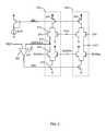
- FIG. 1is a block diagram of one embodiment capable of encoding and transmitting five data bits and a clock on an eight wire communications channel.
- FIG. 2is a block diagram of one embodiment of a receiver compatible with the transmitter of FIG. 1 .
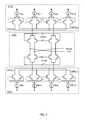
- FIG. 3is a block diagram detailing one embodiment of the clock recovery circuit used by the receiver of FIG. 2 .
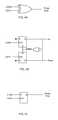
- FIGS. 4A, 4B, and 4Cshow three Phase comparator embodiments suitable for use in a Phase Locked Loop element of a clock recovery circuit.
- FIG. 5is a schematic diagram of one embodiment integrating an XOR phase comparator and clock phase interpolator.
- FIG. 6Ais a schematic diagram of a clocked data latch and FIG. 6B is a schematic diagram of a further embodiment of a clocked data latch integrating a clock phase interpolator.
- FIGS. 7A and 7Bare schematic diagrams of an embodiment integrating a state machine phase comparator and clock phase interpolators.
- FIG. 8is a schematic diagram of one embodiment of a charge pump suitable for further integration with a phase comparator embodiment.
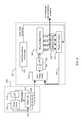
- FIG. 9is a block diagram of a further embodiment in which multiple phases of a reference clock are compared with multiple local clock phases.
- FIG. 10is a block diagram of a further embodiment in which multiple comparisons are made between a single reference clock and multiple local clock phases.
- FIG. 11Ais a weighted XOR phase comparator, in accordance with some embodiments.
- FIG. 11Bis a block diagram of one embodiment of a matrix phase comparison of M reference phases and N local clock phases.
- FIGS. 12A and 12Bare block diagrams of an alternate embodiment of the integrated phase comparator and phase interpolator of FIG. 5 .
- FIG. 13Ais a timing diagram for a folded phase comparator, in accordance with some embodiments.
- FIG. 13Bis timing diagram illustrating a reverse clipping effect, in accordance with some embodiments.
- FIGS. 14A and 14Bare timing diagrams for an array-XOR phase comparator and single-XOR phase comparator, respectively, in accordance with some embodiments.
- FIG. 15is a flowchart of a method, in accordance with some embodiments.
- vector signaling codesmay be used to produce extremely high bandwidth data communications links, such as between two integrated circuit devices in a system.
- multiple data communications channelstransmit symbols of the vector signaling code, acting together to communicate codewords of the vector signaling code.
- the number of channels comprising a communications linkmay range from two to eight or more, and may also communicate one or more clock signals on separate communications channels or as subchannel components of the vector signaling code.
- communication link 120is illustrated as being composed of eight wires 125 , collectively communicating five data values 100 and one clock 105 between transmitter 110 and receiver 130 .
- Individual symbolsmay utilize multiple signal levels, often three or more. Operation at channel rates exceeding 10 Gbps may further complicate receive behavior by requiring deeply pipelined or parallelized signal processing, precluding reception methods in which the previous received value is known as the current value is being received.
- Embodiments described hereincan also be applied to prior art permutation sorting methods not covered by the vector processing methods of [Cronie II], [Cronie III], [Cronie IV], and/or [Tajalli I]. More generally, embodiments can apply to any communication or storage methods requiring coordination of multiple channels or elements of the channel to produce a coherent aggregate result.
- Step Ione typical high-speed receiver embodiment is used for illustrative purposes, without limitation.
- the example data receiverincludes eight identical Continuous Time Linear Equalization (CTLE) stages 210 operating on the signals received on the eight wires, previously shown as 120 in FIG. 1 .
- CTLEContinuous Time Linear Equalization
- vector signaling codesmay be efficiently detected by linearly combining sets of input signals using Multi-Input comparators or mixers (MIC).
- MICMulti-Input comparators
- 5b6w codeused by the example receiver
- five such mixers acting on weighted subsets of the six received data input signalswill detect the five data bits without need of further decoding.
- One additional mixer acting on combinations of the two received clock signalswill similarly detect the clock signal.
- this set of six MIC mixers 220operate on the received and equalized signals to produce detected signals MIC 0 -MIC 5 .
- the five detected data signals MIC 0 -MIC 4are processed in four parallel phases of receive data processing, each phase 230 including five data samplers and subsequent buffering, followed by recombination of the four phase outputs into a received data stream, shown in FIG. 2 as being performed by multiplexers 240 .
- Clock Recovery circuitsalso known in the art as Clock Data Recovery or CDR support such sampling measurements by extracting timing information, either from the data lines themselves or from dedicated clock signal inputs, and utilize that extracted information to generate clock signals to control the time interval used by the data line sampling device(s).
- the actual clock extractionmay be performed using well known circuits such as a Phase Locked Loop (PLL) or Delay Locked Loop (DLL), which in their operation may also generate higher frequency internal clocks, multiple clock phases, etc. in support of receiver operation.
- PLLPhase Locked Loop
- DLLDelay Locked Loop
- the detected clock signalis obtained at MIC 5 and processed 300 to extract properly timed sampling clocks for the four data phases.
- Phase Locked Loopsare well represented in the literature.
- a typical PLLis composed of a phase comparator that compares an external reference signal to an internal clock signal, a low pass filter that smoothes the resulting error value to produce a clock control signal, and a variable frequency clock source (typically, a Voltage Controlled Oscillator or VCO) controlled by the smoothed error value, producing the internal clock signal presented to the phase comparator.
- VCOVoltage Controlled Oscillator
- such a PLL designmay incorporate a clock frequency divider between the VCO and the phase comparator, allowing a higher-frequency clock output to be phase locked to a lower-frequency reference signal.
- variable frequency clock sourceis replaced by a variable delay element, its (optionally multiple tapped) outputs thus representing one or more successive time-delayed versions of the original input signal rather than successive cycles of an oscillator to be phase compared to the reference input signal.
- DLLDelay Locked Loops
- phase comparatorsNumerous forms of phase comparators are known to the art.
- a simple XOR gate as in FIG. 4Amay be used to compare, as a non-limiting example, two square wave signals.
- One familiar with the artwill observe that such a digital XOR output will be a variable-duty-cycle waveform which, when low pass filtered into an analog error signal, results in a proportional error signal centered in its analog signal range when the two input signals have a 90-degree phase offset relationship.
- the more complex state machine phase comparator of FIG. 4Bis composed of two edge-triggered latches clocked respectively by the reference and internal clock signals, with the first received clock edge initiating an output signal on one of the “early” or “late” outputs. Either output becoming active will subsequently cause the latches to reset in anticipation of the next comparison interval.
- Alternative embodimentsmay incorporate a timing delay in this reset path to provide additional control of the reset pulse timing.
- the “late” and “early” phase comparison outputsare typically accepted as “pump up” and “pump down” inputs to a charge pump, the output of which is the analog error value.
- a pump-up signalmay turn on a first transistor circuit that provides charge to capacitor thereby increasing the analog voltage
- a pump down signalmay turn on a second transistor circuit that removes charge from a capacitor, thereby reducing the voltage.
- a zero-degree phase offset between the two input clock signalswill thus leave the analog error value unchanged and the PLL in a stable locked condition.
- a simple edge-clocked “D” flip-flopmay also be used as a phase comparator.
- the D inputsamples the state of the (in this example, square wave) reference input (CkRef); if it is high (e.g. it has already transitioned,) the Q output is high indicating the reference is “early”, if it is low (e.g. it has not yet transitioned,) Q is low indicating the reference is “late”.
- This so-called “bang/bang” phase comparatorprovides a less nuanced error result than the previous example, thus more sophisticated filtering may be performed to obtain loop stability.
- phase comparator typeincorporated in a PLL design
- phase comparator choiceis not limiting.
- Secondary design behaviorsincluding lock time, stability, power consumption, etc. must also be considered as part of the design process.
- the example receiverutilizes a PLL embodiment as shown in FIG. 3 .
- This PLLaccepts the received clock signal R 5 as the reference to which its clocks will be phased locked.
- logic level shift 310is used if appropriate to interface between the signal levels provided by the detecting MIC and the preferred phase comparator input levels.
- Phase Comparator 320compares the reference clock to a local clock derived from the VCO, producing an output which is low pass filtered to provide an Error value which subsequently corrects the operating frequency of VCO 340 .
- the outputs of Phase Comparator 320is a digital waveform requiring conversion to an analog error signal, either through implicit or explicit digital to analog conversion, or by use of an interface element such as a charge pump. Some embodiments may combine such conversion with all or part of the low pass filtering operation, as one example offered without limitation, by the digital filtering behavior shown by the switching action of a charge pump directed by digital control signals generating an analog signal output.
- a ring oscillator 340composed of a sequence of identical gates in a closed loop is used as the internal Voltage Controlled Oscillator (VCO) timing source for the PLL.
- the VCO frequencyis varied by analog adjustment of at least one of: gate propagation delay, inter-gate rise and fall time, and gate switching threshold within the ring oscillator. This may be implemented via switched capacitor banks, where a digital control signal is applied to selective place capacitive elements in parallel and/or series combinations to alter an RC time constant, as one non-limiting example. Still further, a current source that drives a gate of the ring oscillator may be increased or decreased to alter the output switching rise-time/fall-time, and thereby adjust the effective delay.
- VCOVoltage Controlled Oscillator
- Outputs taken at equal intervals (i.e. separated by equal numbers of ring oscillator gates) along the sequence of gates comprising the ring oscillatorprovide the four data phase sampling clocks, herein identified as the 0, 90, 180, and 270 degree clocks.
- the ring oscillatoris composed of eight identical sets of logic gates (e.g., a set of inverter circuits), thus the phase difference from one such set to the next is 45 degrees.
- the 0, 90, 180, and 270 degree outputsmay be obtained, as examples, from the second, fourth, sixth, and eighth outputs.
- the location of the 0 degree tapis arbitrary, as one familiar with the art will recognize that normal PLL behavior will phase align the ring oscillator with the external phase reference regardless of its initial phase.
- Frequency Divider 350divides the VCO outputs by a comparable amount prior to the phase comparator.
- binary (factor of two) dividersare used at 350 to obtain the correct sampling clock rate.
- no divideris used, and the VCO outputs are presented to the phase interpolator directly.
- Each of the four phases of sampling clocksis appropriately timed to sample received data for one of the four parallel processing phases.
- internal clock ph 000is aligned to optimally trigger data samplers in the phase 0 phase of processing, clock ph 090 in phase 1 , clock ph 180 in phase 2 , and clock ph 270 in phase 3 .
- phase interpolator 360the local clock output presented to the phase comparator is obtained from phase interpolator 360 , the output phase of which is controllably intermediate between its input clock phases.
- the PLLmay lock with its fixed phase relationship, while the internal clock signals obtained from ring oscillator 340 will be offset from that fixed phase by the phase delay amount introduced by phase interpolator 350 , as controlled by signal Phase offset correction.
- Phase interpolatorsare known in the art, examples being provided by [Buchwald I] and [Tajalli II].
- phase interpolator 360receives multiple local clock phases from the ring oscillator 340 having 90 degree phase differences. Said phase interpolator may be controlled to select two adjacent clock input phases and then to interpolate between them so as to produce an output at a chosen phase offset between the two selected values. For purposes of description, it may be assumed that a phase comparator design is used which drives the PLL to lock with a zero phase differential between the two phase comparator inputs. Thus, continuing the example, applying the 0 and 90 degree clock phases as inputs to the phase interpolator allows adjustment such that the PLL leads the reference clock input by between 0 and 90 degrees.
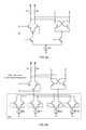
- FIG. 5An embodiment providing improved response characteristics suitable for such high-speed operation is illustrated in FIG. 5 .
- thisis a CMOS design providing symmetrical operation for both positive and negative output excursions, integrating elements of both phase interpolator and phase comparator designs. This tight integration results in reduced node capacitances, facilitating the desirable high speed operation, and the balanced differential structure simplifies the control of charge and discharge currents.
- the PLL VCO(or a clock divider driven by said VCO) provides the local oscillator inputs to phase interpolator elements 510 and 515 , which together set the effective local clock phase.
- Four local oscillator phases with 90-degree offsetare shown i.e. equivalent to two phases in quadrature relationship and their complimentary signals and thus identified as +I, +Q, and ⁇ I, ⁇ Q, permitting a full 360 degree or “four quadrant” phase adjustment.
- Other embodimentsmay utilize as few as two local oscillator phases, may use oscillator phases having other than 90-degree phase differences, or may select clock phases from an input set of more than four; as one non-limiting example, choosing at least two clock phases to be interpolated between from an input set of eight clock phases.
- phase interpolator element 510includes four mixing elements, each mixing element comprising a differential transistor pair and a controlled current source, with a common differential output driven by the four mixing elements in parallel.
- configuration of current source IA(i)controls the amount of local oscillator phase +I presented to the common output ckp; similarly, current source IA( ⁇ i) controls the amount of complimentary output phase ⁇ I in the output, IA(q) controls the amount of +Q, and IA( ⁇ q) controls the amount of ⁇ Q.
- configuration of the four current sourcescan produce an output clock at Ckp having any desired phase relationship to the PLL local clock input.
- phase interpolator element 515 current sources IB(i), IB( ⁇ i), IB(q), and IB( ⁇ q)may be configured to obtain an output clock at Ckn having any desired phase relationship to the PLL local clock input.
- CkPLLp and CkPLLnmay be configured to have complimentary relationships to provide phase comparator 520 with balanced and complimentary positive- and negative-going current amplitudes.
- configuration with non-complimentary IA and IB valuesmay be performed to obtain particular results.
- an embodiment separately adjusting IA and IB valuesmight obtain higher resolution phase adjustment, compared to an embodiment maintaining perfectly complimentary IA and IB values.
- the second input to the phase comparator 520is external reference clock CkRef+/CkRef ⁇ , producing the phase error output currents VCOctl+/VCOctl ⁇ .
- the two external reference clocksare of opposing polarity but not necessarily complementary phase, thus the positive polarity comparison and negative polarity comparison represent different phase comparisons.
- Such an advanced embodimentmay be combined with non-complimentary IA and IB bias configurations, providing independent adjustment of local clock phase during those different phase comparisons.
- the CkRef input at the top of PD 520is a first phase selected from the reference clock phases available in the circuit, and the IA currents are adjusted to provide a corresponding interpolated phase offset from the first selected phase, and the CkRef input at the bottom of PD 520 is a second phase selected from the reference clock phases available in the circuit, and the IB currents are adjusted to provide a corresponding interpolated phase offset from the second selected phase, wherein the amount of the relative phase offsets are the same.
- Configuration of phase interpolator current source valuesmay be performed by external control logic, including without limitation, a hardware configuration register, control processor output register, and hardware CDR adjustment logic.
- Phase comparator 520 in the embodiment of FIG. 5is shown as an XOR-style device as in FIG. 4A , mixing local clock CkPLL and external reference clock CkRef to produce phase error output VCOctl.
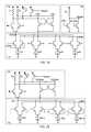
- a folded phase comparatoris used at 1220 , driven by currents produced by the combination of phase interpolator 510 and current sink Ifix 2 , and the combination of phase interpolator 520 and current source Ifix 1 .
- the folded phase comparator embodiment shown in FIG. 12Ais described in further detail below.
- current sources IA(i), IA( ⁇ i), IA(q), and IA( ⁇ q)are configured to produce the desired interpolation of PLL clocks i, q, and ⁇ q in interpolator outputs CkPLLp and CkPLLp
- current sources IB(i), IB( ⁇ i), IB(q), and IB( ⁇ q)are configured to produce the desired interpolation of PLL clocks i, ⁇ i, q, and ⁇ q in interpolator outputs CkPLLn and CkPLLn .
- Phase comparator 1220is also driven by received reference clocks CkRef+ and CkRef ⁇ , producing phase comparison results Phase Error (+) and Phase Error ( ⁇ ).
- the circuit node labeled Circuit Balance Feedbackmay be monitored to determine the relative DC component of the interpolated clock signals, which may then be modified by adjustment of the configured current source values in 510 and 515 .
- each current source IA and IBreceives seven control bits. It should be noted that embodiments are not limited to receiving seven control bits, and that any number of control bits may be implemented according to design constraints for PI resolution, for example.
- the PIs 510 and 515have 7 bits of resolution.
- additional resolutionmay be implemented by introducing a shift in IB with respect to IA, or vice versa.
- IAIB+8, where 8 is a decimal shift added to the control bits of each current source IA to obtain the control bits of each current source IB.
- the P-side PI 510 and N-side PI 515are receiving two different VCO phases, and the phase comparator collects information from different phases of the VCO. Since the PIs 510 and 515 combine information from different phases of VCO, the PLL has more detailed information about phases of PLL and the bandwidth of the PLL is higher than a conventional PLL.
- the first partial phase comparator(N-side XOR) compares the phase of reference with one set of VCO feedback phases, and a second partial phase comparator (P-side XOR) that compares the reference clock phase with a second set of VCO feedback phases.
- N-side XORcompares the phase of reference with one set of VCO feedback phases
- P-side XORa second partial phase comparator that compares the reference clock phase with a second set of VCO feedback phases.
- a folded structure as shown in FIG. 12Amay be used.
- FIG. 12Ais similar to the embodiment shown in FIG. 5 , however the phase comparator 520 is replaced with a folded phase comparator 1220 .
- folded phase comparator 1220includes current sources Ifix 1 and Ifix 2 , which may be configured to provide more voltage headroom to the PMOS PI current sources IA and the NMOS PI current sources IB.
- phase comparator 1220includes a pair of transistor branches connected to CkPLLp and CkPLLn. For purposes of illustration, consider PI 510 and 515 only having IA(i) and IB(i) turned on respectively, representing phase ph 0000 from the VCO.
- the folded phase comparator 1220will be in lock condition.
- current Ipis charged to the ( ⁇ ) terminal of the Phase Error signal through transistor 1206 using PMOS PI 510 .
- current Inis discharged from the ( ⁇ ) terminal of the Phase Error signal through transistor 1208 using NMOS PI 515 .
- current Ipis charged from the (+) terminal of the Phase error signal through transistor 1202 , while current In is discharged from the (+) terminal through transistor 1204 .
- Ifix 2will sink a fixed amount of current being provided from PMOS PI 510
- Ifix 1sources some current to NMOS PI 515 to prevent the current sources in the NMOS PI from sinking too much current from the Phase Error signal.
- Such a techniqueprovides a reverse clipping effect.
- One of skill in the artmay notice that equally adjusting the Ifix current magnitudes may have an effect on the range of the Phase Error signal. In some embodiments, increasing the Ifix magnitudes will lower the magnitude range of the Phase Error signal, while decreasing the Ifix magnitudes will increase the magnitude range of the Phase Error signal. This relationship is illustrated by FIG. 13B .
- FIG. 13Bis a timing diagram illustrating the reverse clipping feature described above.
- the second 180 degrees ( 4 )may be used to provide circuit balance feedback, as shown in FIG. 12A .
- currentmay be charged via the PMOS PI 510 while current is discharged via the NMOS PI 515 . If there is an imbalance of charge/discharge currents, a non-zero circuit balance feedback signal may indicate this imbalance, which may occur due to transistor mismatches, for example.
- the circuit balance feedback signalmay then be used to adjust either Ifix 1 or Ifix 2 to balance the charge/discharge currents so that the balance feedback signal is zero.
- FIG. 12BA simplified schematic of the phase comparator circuit of FIG. 12A is shown in FIG. 12B .
- phase comparator of [Tajalli IV]may alternatively be used at 520 or 1220 , providing equivalent phase detection with enhanced signal headroom in embodiments utilizing low power supply voltages.
- Other phase comparatorsincluding all variations shown in FIGS. 4A, 4B, and 4C , may also be substituted at 520 in that embodiment.
- the State Machine Phase/Frequency Detector of FIG. 4Bmay be combined with the Phase Interpolator design of FIG. 5 .
- FIG. 6Ashows a schematic of one embodiment of a conventional CIVIL clocked latch, composed of a clocked feedback latch outputting results Q and Q the state of which is initialized by clocked differential inputs D and D .
- FIG. 6Bshows the same circuit in which the clock source phase is modified by phase interpolator 615 , operation of which is as previously described for FIG. 5 .
- D flip-flop 710is clocked by the received clock CkRef, which is passed through phase interpolator 715 .
- current source IAwould be set to “mix” input CkRef at 100% proportion, and the other three current sources set to zero current.
- D flip-flop 720is clocked by local clock CkPLL, which is obtained by configuration of phase interpolator 725 current sources IB(i), IB( ⁇ i), IB(q), and IB( ⁇ q), which in turn controls the relative proportions and polarities of I and Q clocks being combined.
- Iis obtained from ph 000 , ⁇ I from ph 180 , Q from ph 090 , and ⁇ Q from ph 270 , as seen in FIG. 3 .
- a simple CML OR gate 730drives the reset function for flip-flops 710 and 720 .
- phase interpolator 715is functionally disabled and retained only to preserve the same parasitic load characteristics as are presented by active phase interpolator 725 , to maximize circuit symmetry and maintain balanced loading characteristics to minimize secondary effects such as detection bias and drift.
- PLL phase comparator outputsare typically used to drive a charge pump circuit (CPC), the output of which is an analog error signal used to control the VCO.
- CPCcharge pump circuit
- the described improvement from reduced capacitance and resulting higher circuit speed in integrating the PLL phase comparator and clock adjustment phase interpolatormay be further extended by also integrating elements of the charge pump in the same manner.
- the charge pump control signals UPp, UPn, DOWNp, and DOWNnprovided by the embodiment shown in FIGS. 7A and 7B directly control the charge pump embodiment of FIG. 8 to produce output I OUT .
- Current source I CPC and voltage reference V REFmay be configured to scale and adjust the I OUT range.
- One familiar with the artwill note the significant symmetry in the circuit of FIG. 8 , allowing accurate tracking between generation of V REPLICA and I OUT signals.
- FIG. 8is a schematic of a charge pump circuit with improved charge/discharge current balancing, in accordance with some embodiments.
- the circuit 800includes two parallel charge pumps 802 , 804 : the two differential pairs within charge pump 804 generate an output current representing a phase error signal in response to the up and down pulses, and the two differential pairs of charge pump 802 are used to set the discharge current to be equal to the charge current as described below.
- the current source I CPCsets a charging current level by providing a corresponding bias voltage V BP through a current mirroring circuit to drive the top current sources 806 , 808 of the two charge pumps so as to also provide I CPC to each charge pump 802 , 804 .
- the node 812When UPn goes low and turns on field effect transistor (FET) 810 , the node 812 is charged (capacitive element 814 is either a discrete cap or a parasitic cap) by the charging current I CPC provided by FETs 806 , 810 . In a balanced condition (i.e., in the absence of a phase error), the amount of current that is then discharged during a high DOWNp signal through the bottom FET 816 should bring the node 812 back to the V REF value.
- FETfield effect transistor
- the amplifier 820will increase the bias voltage V BN to the discharge-current FET 818 to increase the amount of discharge current so that it equals the charge current I CPC and the voltage V REPLICA at node 812 is brought back to V REF .
- the discharge current set by V BN on FET 818is too high, the V REPLICA voltage drops too low, and the amplifier 820 responsively reduces the bias voltage V BN on discharge-FET 818 to bring the charge pump currents into equilibrium.
- phase comparatorphase interpolator
- charge pump elementsOther embodiments may be obtained by equivalent combination of phase comparator, phase interpolator, and charge pump elements.
- phase interpolatorsstems from the different nature of the local clock and reference clock sources.
- the formeris obtained from a multiphase clock source (e.g. an oscillator or divider) inherently capable of providing the multiphase inputs for use by a phase interpolation element.
- the latteris generally single phased, obtained from (typically) one received clock source.
- a received clock passing through such a delay lineproduces a resulting set of outputs which take on some of the characteristics of a multiphase clock.
- the equal-interval outputs of a four-tap delay line having an overall delay comparable to the reference clock periodwill provide outputs having similar characteristic to quadrature phased clock signals.
- each such outputis phase compared to an appropriately-selected local clock phase, a series of phase error results will be produced which may be combined to produce a more accurate aggregate clock error signal for the PLL VCO.
- the delayed versions of the receive clockrepresent additional opportunities for phase comparison with a clock derived from the VCO, thus providing a higher update rate for the controlled loop, and thus improved PLL loop bandwidth leading to reduced jitter and better noise immunity. That is, using this technique, the update rate of the loop will be increased, which in turn enables the circuit to track and correct the effects of noise and jitter at higher frequencies.
- the delay intervals provided by the delay linemust be coordinated with the period between local clock phases, with such controls giving the delay element many of the aspects of a Delay-Locked Loop (DLL.)
- DLLDelay-Locked Loop
- the external clock reference input to the previous PLL embodiment 300is provided by DLL 910 .
- the received clock signal R 5is presented to tapped delay line 916 , producing a series of received clock phases 918 .
- the DLL control loopis provided by phase comparator 912 comparing the received clock with a delayed clock, producing an error value that is low pass filtered 915 , producing a delay adjust signal controlling the delay line timing.
- multi-phase comparator 920the previous simple phase comparison ( 320 of FIG. 3 ) is now performed by multi-phase comparator 920 .
- Each XOR gate output representing a partial phase error signalmay be converted to an analog signal value, all such analog partial phase error signals being summed using a summation circuit 935 to produce a composite phase error signal for controlling ring oscillator 340 , as previously described.
- summation 935is performed by a weighted summation node comparable to the previously-described MIC mixer, the different selected weights of said summation allowing further control of PLL static and dynamic operational characteristics.
- each XOR outputmay be used to drive a separate transistor circuit for injecting or removing charge from a capacitive element to achieve the summation.
- the PLL 340 of FIG. 9may be configured to provide a desired phase offset, where the interpolated phases each have the same offset relative the tap delay line signal to which it will be XOR compared.
- the described multi-phase reference clockmay be directly available from the receiver, as one example where the communications protocol incorporates multiple clock signals.
- FIG. 10shows an embodiment in which the single received reference signal 1018 enters multi-phase comparator 920 in which the single received reference signal is compared to each of two or more phases of local clock signal 965 .
- XOR partial phase comparatorsform partial phase error signals by comparing the phase of the single received reference clock phase 918 with a different phase of the local clock signal 965 from phase interpolator 360 .
- Each partial phase error signalmay be converted to an analog signal value, all such analog partial phase error signals being summed to produce a composite phase error signal for controlling ring oscillator 340 , as previously described.
- summation 935is performed by a weighted summation node comparable to the previously described MIC mixer, the different selected weights of said summation allowing further control of PLL static and dynamic operational characteristics.
- weight adjustmentsmay be used to produce additional closed-loop poles and/or zeroes in the PLL time domain transfer function, providing additional control of loop stability.
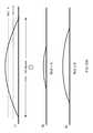
- FIG. 14Ais a timing diagram of a reference signal CKREF being compared with four phases of the VCO (feedback from the PLL):
- FIG. 14Afurther includes a summation of the four XOR outputs. As can be seen, in lock condition, the integral of the bottom waveform is zero, and the PLL will lock properly.
- FIG. 14Bhas been included to illustrate a conventional XOR based phase comparators in which the reference is compared to only one VCO phase. In lock position, the reference and VCO are 90-degree phase shifted, and the output of XOR is a rectangular waveform with an average value equal to zero.
- the two waveformssimple XOR in the FIG.
- the weights of said summationare configured such that they decline in proportion to the timing difference of the comparison clock phase relative to the PLL “normal lock” phase.
- the comparison of ph 090 and the received reference signalis weighted 1 ; comparisons of ph 000 and ph 180 (e.g. one tap offset from the normal lock phase) are weighted 1 ⁇ 2; comparison of the received reference signal and ph 270 (two tap offsets from the normal lock phase) is weighed 1 ⁇ 4; etc.
- These various weighted comparison resultsare then summed to produce a composite signal which when low pass filtered 330 , is the Error value controlling PLL VCO 340 .
- the deterministic jitter produced by the multiple phase comparisonswas seen to occur at a 12.5 GHz rate with equal phase comparator weights. Even though the amount of jitter was very small and the jitter rate was well above the loop filter cutoff frequency, the deterministic jitter was significantly reduced with the described weight adjustments, in which weight magnitudes decline in proportion to their offset distance from the primary reference signal sample.
- different weighted valuesare used in a comparator circuit to construct a discrete time domain filter. This property can be used to simplify the design of analog filter 330 . For example, with proper weighting values one might construct a discrete time domain zero in the transfer function that provides conditions to make the loop robust.
- phase comparatorphase interpolator
- charge pump elementscharge pump elements
- the multi-phase comparison of multiple phases derived from a received reference signal and multiple phases derived from the local PLL clockmay be generalized into a matrix phase comparator, one embodiment of which is shown in FIG. 11B , with one embodiment of each individual phase comparator 1110 (which may be referred to in FIG. 11B as a partial phase comparator) in the matrix shown in FIG. 11A as single-phase comparator 1110 .
- a matrix phase comparatorone embodiment of which is shown in FIG. 11B
- each individual phase comparator 1110which may be referred to in FIG. 11B as a partial phase comparator
- FIG. 11Asingle-phase comparator 1110 .
- partial phase comparators arranged in a four by four matrixare illustrated, with no limitation implied by those illustrative choices.
- Embodimentsmay be organized into rectangular, square, or sparse matrices of any dimensions M and N, with elements of the matrix being composed of any partial phase comparator described herein and optionally any weighting factor computation described herein.
- each of M phases derived from the received reference signalis separately phase compared with each of the N phases derived from the local clock, which may be received from a PLL, or alternatively directly from a VCO or various other clock sources.
- the N phases of the local clockare received from the PLL.
- Each resulting phase error signalis weighted by a configured or predetermined amount, with all (M*N) weighted results summed to produce an aggregate error result.
- An example of one phase comparatoris shown in FIG. 11A as 1110 , composed of XOR phase comparator 1112 feeding to result weighting factor 1118 .
- An embodiment of the complete matrix phase comparator 1120 in FIG. 11Bis composed of M*N instances of partial phase comparator 1110 , each partial phase comparator accepting one of the M phases of the reference signal, herein identified as CkRef 0 , CkRef 1 , CkRef 2 , CkRef 3 , and one of the N phases of the local clock phase inputs herein identified as CkPLL 0 , CkPLL 1 , CkPLL 2 , CkPLL 3 , and producing a weighted result e.g. multiple partial phase error signals 1131 , 1132 , 1133 , 1134 as input to summation 935 , which produces a composite phase error signal 1145 .
- the previously-described multi-phase comparator 920 of FIG. 9is equivalent to a partially-populated instance of the present matrix comparator, i.e. having comparators instantiated across a diagonal of the matrix. Functionally, an identical result may be obtained from a full matrix by setting the weights along such a diagonal to a nonzero value, and all other comparator weights to zero. It thus follows that other described behaviors including simulation of phase offsets, introduction of loop time domain zeroes, etc. may be similarly be obtained by selective configuration of matrix weighting factors.
- FIG. 15illustrates a flowchart of method 1500 , in accordance with some embodiments.
- method 1500includes receiving N phases of a local clock signal and M phases of a reference signal at block 1502 , wherein M is an integer greater than or equal to 1 and N is an integer greater than or equal to 2.
- the methodfurther includes generating a plurality of partial phase error signals at block 1504 , each partial phase error signal formed at least in part by comparing (i) a respective phase of the M phases of the reference signal to (ii) a respective phase of the N phases of the local clock signal.
- a composite phase error signalis generated by summing the plurality of partial phase error signals, and responsively a fixed phase of a local oscillator is adjusted 1508 using the composite phase error signal.
- the plurality of partial phase error signalscomprises M ⁇ N partial phase error signals, and each phase of the N phases of the local clock signal is compared to each phase of the M phases of the reference signal.
- each partial phase error signal of the plurality of partial phase error signalshas a corresponding weight applied to it.
- the M phases of the reference signalare received from a delay-lock loop operating on an input reference signal.
- At least one of the N phases of the local clock signalis generated using a phase interpolator operating on local oscillator signals and a phase offset signal. In some embodiments, at least one of the N phases of the local clock signal comprises interpolating 4 phases using 4 differential pairs in the phase interpolator, each of the 4 phases being interpolated according to a corresponding differential pair connected to an independently tunable current source.
- At least one partial phase error signalis generated using a pair of flip-flops, wherein a first flip-flop of the pair of flip-flops is clocked using a given phase of the M phases of the reference signal and a second flip-flop is clocked using a given phase of the N phases of the local clock signal.
- each partial phase error signalis an analog signal generated using a respective charge pump, the respective charge pump receiving respective charge pump control signals generated by a respective comparison between the respective phase of the M phases of the reference signal and the respective phase of the N phases of the local clock signal.
- the clock signal received from MIC 5 in FIG. 2 after being transported over two dedicated clock wirescould just as easily be received from, as one example MIC 4 , having been transported as one subchannel of the vector signaling code also carrying the data.
- This method of embedding the clock in a vector signaling code subchannelis described in [Shokrollahi II] and [Holden III]. All of the described clock embedding embodiments therein may be beneficially combined with the PLL and timing control mechanisms described herein, without limitation.
Landscapes
- Engineering & Computer Science (AREA)
- Computer Networks & Wireless Communication (AREA)
- Signal Processing (AREA)
- Physics & Mathematics (AREA)
- Nonlinear Science (AREA)
- Power Engineering (AREA)
- Stabilization Of Oscillater, Synchronisation, Frequency Synthesizers (AREA)
Abstract
Description
This application claims the benefit of U.S. Provisional Application No. 62/326,591 filed Apr. 22, 2016, entitled “HIGH PERFORMANCE PHASE LOCKED LOOP”, naming Armin Tajalli, which is hereby incorporated by reference in its entirety.
The following prior applications are herein incorporated by reference in their entirety for all purposes:
U. S. Patent Publication 2011/0268225 of application Ser. No. 12/784,414, filed May 20, 2010, naming Harm Cronie and Amin Shokrollahi, entitled “Orthogonal Differential Vector Signaling” (hereinafter “Cronie I”).
U. S. Patent Publication 2011/0302478 of application Ser. No. 12/982,777, filed Dec. 30, 2010, naming Harm Cronie and Amin Shokrollahi, entitled “Power and Pin Efficient Chip-to-Chip Communications with Common-Mode Resilience and SSO Resilience” (hereinafter “Cronie II”).
U.S. patent application Ser. No. 13/030,027, filed Feb. 17, 2011, naming Harm Cronie, Amin Shokrollahi and Armin Tajalli, entitled “Methods and Systems for Noise Resilient, Pin-Efficient and Low Power Communications with Sparse Signaling Codes” (hereinafter “Cronie III”).
U.S. patent application Ser. No. 13/176,657, filed Jul. 5, 2011, naming Harm Cronie and Amin Shokrollahi, entitled “Methods and Systems for Low-power and Pin-efficient Communications with Superposition Signaling Codes” (hereinafter “Cronie IV”).
U.S. patent application Ser. No. 13/542,599, filed Jul. 5, 2012, naming Armin Tajalli, Harm Cronie, and Amin Shokrollhi entitled “Methods and Circuits for Efficient Processing and Detection of Balanced Codes” (hereafter called “Tajalli I”.)
U.S. patent application Ser. No. 13/842,740, filed Mar. 15, 2013, naming Brian Holden, Amin Shokrollahi and Anant Singh, entitled “Methods and Systems for Skew Tolerance in and Advanced Detectors for Vector Signaling Codes for Chip-to-Chip Communication”, hereinafter identified as [Holden I];
U.S. Provisional Patent Application No. 61/946,574, filed Feb. 28, 2014, naming Amin Shokrollahi, Brian Holden, and Richard Simpson, entitled “Clock Embedded Vector Signaling Codes”, hereinafter identified as [Shokrollahi I].
U.S. patent application Ser. No. 14/612,241, filed Aug. 4, 2015, naming Amin Shokrollahi, Ali Hormati, and Roger Ulrich, entitled “Method and Apparatus for Low Power Chip-to-Chip Communications with Constrained ISI Ratio”, hereinafter identified as [Shokrollahi II].
U.S. patent application Ser. No. 13/895,206, filed May 15, 2013, naming Roger Ulrich and Peter Hunt, entitled “Circuits for Efficient Detection of Vector Signaling Codes for Chip-to-Chip Communications using Sums of Differences”, hereinafter identified as [Ulrich I].
U.S. patent application Ser. No. 14/816,896, filed Aug. 3, 2015, naming Brian Holden and Amin Shokrollahi, entitled “Orthogonal Differential Vector Signaling Codes with Embedded Clock”, hereinafter identified as [Holden II].
U.S. patent application Ser. No. 14/926,958, filed Oct. 29, 2015, naming Richard Simpson, Andrew Stewart, and Ali Hormati, entitled “Clock Data Alignment System for Vector Signaling Code Commuications Link”, hereinafter identified as [Stewart I].
U.S. patent application Ser. No. 14/925,686, filed Oct. 28, 2015, naming Armin Tajalli, entitled “Advanced Phase Interpolator”, hereinafter identified as [Tajalli II].
U.S. Provisional Patent Application No. 62/286,717, filed Jan. 25, 2016, naming Armin Tajalli, entitled “Voltage Sampler Driver with Enhanced High-Frequency Gain”, hereinafter identified as [Tajalli III].
The following additional references to prior art have been cited in this application:
U.S. Pat. No. 6,509,773, filed Apr. 30, 2001 by Buchwald et al., entitled “Phase interpolator device and method” (hereafter called [Buchwald].
“Linear phase detection using two-phase latch”, A. Tajalli, et al., IEE Electronic Letters, 2003, (hereafter called [Tajalli IV].)
“A Low-Jitter Low-Phase-Noise 10-GHz Sub-Harmonically Injection-Locked PLL With Self-Aligned DLL in 65-nm CMOS Technology”, Hong-Yeh Chang, Yen-Liang Yeh, Yu-Cheng Liu, Meng-Han Li, and Kevin Chen, IEEE Transactions on Microwave Theory and Techniques, Vol 62, No. 3, March 2014 pp. 543-555, (hereafter called [Chang et al.])
“Low Phase Noise 77-GHz Fractional-N PLL with DLL-based Reference Frequency Multiplier for FMCW Radars”, Herman Jalli Ng, Rainer Stuhlberger, Linus Maurer, Thomas Sailer, and Andreas Stelzer, Proceedings of the 6th European Microwave Integrated Circuits Conference, 10-11 Oct. 2011, pp. 196-199, (hereafter called [Ng et al.])
“Design of Noise-Robust Clock and Data Recovery using an Adaptive-Bandwidth Mixed PLL/DLL”, Han-Yuan Tan, Doctoral Thesis, Harvard University November 2006, (hereafter called [Tan]).
The present embodiments relate to communications systems circuits generally, and more particularly to obtaining a stable, correctly phased receiver clock signal from a high-speed multi-wire interface used for chip-to-chip communication.
In modern digital systems, digital information has to be processed in a reliable and efficient way. In this context, digital information is to be understood as information available in discrete, i.e., discontinuous values. Bits, collection of bits, but also numbers from a finite set can be used to represent digital information.
In most chip-to-chip, or device-to-device communication systems, communication takes place over a plurality of wires to increase the aggregate bandwidth. A single or pair of these wires may be referred to as a channel or link and multiple channels create a communication bus between the electronic components. At the physical circuitry level, in chip-to-chip communication systems, buses are typically made of electrical conductors in the package between chips and motherboards, on printed circuit boards (“PCBs”) boards or in cables and connectors between PCBs. In high frequency applications, microstrip or stripline PCB traces may be used.
Common methods for transmitting signals over bus wires include single-ended and differential signaling methods. In applications requiring high speed communications, those methods can be further optimized in terms of power consumption and pin-efficiency, especially in high-speed communications. More recently, vector signaling methods have been proposed to further optimize the trade-offs between power consumption, pin efficiency and noise robustness of chip-to-chip communication systems. In such vector signaling systems, digital information at the transmitter is transformed into a different representation space in the form of a vector codeword that is chosen in order to optimize the power consumption, pin-efficiency and speed trade-offs based on the transmission channel properties and communication system design constraints. Herein, this process is referred to as “encoding”. The encoded codeword is communicated as a group of signals from the transmitter to one or more receivers. At a receiver, the received signals corresponding to the codeword are transformed back into the original digital information representation space. Herein, this process is referred to as “decoding”.
Regardless of the encoding method used, the received signals presented to the receiving device must be sampled (or their signal value otherwise recorded) at intervals best representing the original transmitted values, regardless of transmission channel delays, interference, and noise. Such Clock and Data Recovery (CDR) not only determines the appropriate sample timing, but may continue to do so continuously, providing dynamic compensation for varying signal propagation conditions.
Many known CDR systems utilize a Phase-Locked Loop (PLL) or Delay-Locked Loop (DLL) to synthesize a local receive clock having an appropriate frequency and phase for accurate receive data sampling.
To reliably detect the data values transmitted over a communications system, a receiver must accurately measure the received signal value amplitudes at carefully selected times. Various methods are known to facilitate such receive measurements, including reception of one or more dedicated clock signals associated with the transmitted data stream, extraction of clock signals embedded within the transmitted data stream, and synthesis of a local receive clock from known attributes of the communicated data stream.
In general, the receiver embodiments of such timing methods are described as Clock-Data Recovery (CDR), often based on Phase-Lock Loop (PLL) or Delay-Locked Loop (DLL) synthesis of a local receive clock having the desired frequency and phase characteristics.
In both PLL and DLL embodiments, a phase comparator compares the relative phase (and in some variations, the relative frequency) of a received reference signal and a local clock signal to produce an error signal, which is subsequently used to correct the phase and/or frequency of the local clock source and thus minimize the error. As this feedback loop behavior will lead to a given PLL embodiment producing a fixed phase relationship (as examples, 0 degrees or 90 degrees of phase offset) between the reference signal and the local clock, an additional fixed or variable phase adjustment is often introduced to permit the phase offset to be set to a different desired value (as one example, 45 degrees of phase offset) to facilitate receiver data detection.
Below, methods and systems are described for receiving N phases of a local clock signal and M phases of a reference signal, wherein M is an integer greater than or equal to 1 and N is an integer greater than or equal to 2, generating a plurality of partial phase error signals, each partial phase error signal formed at least in part by comparing (i) a respective phase of the M phases of the reference signal to (ii) a respective phase of the N phases of the local clock signal, and generating a composite phase error signal by summing the plurality of partial phase error signals, and responsively adjusting a fixed phase of a local oscillator using the composite phase error signal.
In some embodiments, M=1, and N partial phase error signals are summed to generate the composite phase error signal. Alternatively, the plurality of partial phase error signals includes M=N partial phase error signals, and wherein a given phase of the N phases of the local clock signal and a given phase of the M phases of the reference signal are each used to generate a single partial phase error signal. In further alternative embodiments, the plurality of partial phase error signals includes M×N partial phase error signals, and wherein each phase of the N phases of the local clock signal is compared to each phase of the M phases of the reference signal.
In some embodiments, each partial phase error signal of the plurality of partial phase error signals has a corresponding weight applied to it. In some embodiments, the weights are selected according to an M×N matrix.
In some embodiments, the M phases of the reference signal are received from a delay-lock loop operating on an input reference signal.
In some embodiments, at least one of the N phases of the local clock signal is generated using a phase interpolator operating on local oscillator signals and a phase offset signal. In some embodiments, generating at least one of the N phases of the local clock signal includes interpolating 4 phases using 4 differential pairs in the phase interpolator, each of the 4 phases being interpolated according to a corresponding differential pair connected to an independently tunable current source.
In some embodiments, at least one partial phase error signal is generated using a pair of flip-flops, wherein a first flip-flop of the pair of flip-flops is clocked using a given phase of the M phases of the reference signal and a second flip-flop is clocked using a given phase of the N phases of the local clock signal.
In some embodiments, each partial phase error signal is an analog signal generated using a respective charge pump, the respective charge pump receiving respective charge pump control signals generated by a respective comparison between the respective phase of the M phases of the reference signal and the respective phase of the N phases of the local clock signal.
Embodiments are described in which the Phase Detection and phase adjustment elements are combined, leading to lower circuit node capacitance and reduced circuit delays, these improvements in turn enabling increased loop stability and improved PLL lock characteristics, including increased loop lock bandwidth leading to lower clock jitter and improved power supply noise rejection.
Embodiments are also described in which a Delay-Locked Loop is used to convert the received reference clock signal into multiple reference clock phases, converting the PLL phase comparison operation into multiple comparisons made between a reference clock phase and a local clock phase. A summation or weighted summation of the multiple comparison results is then used as the error feedback signal for the PLL. A further embodiment is described in which multiple comparisons are made between a single received reference clock phase and multiple local clock phases, with the weighted sum of the multiple comparison results used as the error feedback term for the PLL. In at least one such further embodiment, said weighted sums comprise a two dimensional time domain filter.
As described in [Cronie I], [Cronie II], [Cronie III] and [Cronie IV], vector signaling codes may be used to produce extremely high bandwidth data communications links, such as between two integrated circuit devices in a system. As illustrated by the embodiment ofFIG. 1 , multiple data communications channels transmit symbols of the vector signaling code, acting together to communicate codewords of the vector signaling code. Depending on the particular vector signaling code used, the number of channels comprising a communications link may range from two to eight or more, and may also communicate one or more clock signals on separate communications channels or as subchannel components of the vector signaling code. In the example ofFIG. 1 ,communication link 120 is illustrated as being composed of eightwires 125, collectively communicating fivedata values 100 and oneclock 105 betweentransmitter 110 andreceiver 130.
Individual symbols, e.g. transmissions on any single communications channel, may utilize multiple signal levels, often three or more. Operation at channel rates exceeding 10 Gbps may further complicate receive behavior by requiring deeply pipelined or parallelized signal processing, precluding reception methods in which the previous received value is known as the current value is being received.
Embodiments described herein can also be applied to prior art permutation sorting methods not covered by the vector processing methods of [Cronie II], [Cronie III], [Cronie IV], and/or [Tajalli I]. More generally, embodiments can apply to any communication or storage methods requiring coordination of multiple channels or elements of the channel to produce a coherent aggregate result.
Receiver Data Detection
To provide context for the following examples, one typical high-speed receiver embodiment [Stewart I] is used for illustrative purposes, without limitation.
As illustrated inFIG. 2 , the example data receiver includes eight identical Continuous Time Linear Equalization (CTLE) stages210 operating on the signals received on the eight wires, previously shown as120 inFIG. 1 .
As described in [Tajalli I], [Holden I] and [Ulrich I], vector signaling codes may be efficiently detected by linearly combining sets of input signals using Multi-Input comparators or mixers (MIC). For the 5b6w code used by the example receiver, five such mixers acting on weighted subsets of the six received data input signals will detect the five data bits without need of further decoding. One additional mixer acting on combinations of the two received clock signals will similarly detect the clock signal. InFIG. 2 , this set of sixMIC mixers 220 operate on the received and equalized signals to produce detected signals MIC0-MIC5.
Because of the high data rates involved, multiple parallel phases of receive processing may be used in the example receiver. In one embodiment, the five detected data signals MIC0-MIC4 are processed in four parallel phases of receive data processing, eachphase 230 including five data samplers and subsequent buffering, followed by recombination of the four phase outputs into a received data stream, shown inFIG. 2 as being performed bymultiplexers 240.
Clock Recovery circuits (also known in the art as Clock Data Recovery or CDR) support such sampling measurements by extracting timing information, either from the data lines themselves or from dedicated clock signal inputs, and utilize that extracted information to generate clock signals to control the time interval used by the data line sampling device(s). The actual clock extraction may be performed using well known circuits such as a Phase Locked Loop (PLL) or Delay Locked Loop (DLL), which in their operation may also generate higher frequency internal clocks, multiple clock phases, etc. in support of receiver operation. In the embodiment ofFIG. 2 , the detected clock signal is obtained at MIC5 and processed300 to extract properly timed sampling clocks for the four data phases.
PLL Overview
Phase Locked Loops are well represented in the literature. A typical PLL is composed of a phase comparator that compares an external reference signal to an internal clock signal, a low pass filter that smoothes the resulting error value to produce a clock control signal, and a variable frequency clock source (typically, a Voltage Controlled Oscillator or VCO) controlled by the smoothed error value, producing the internal clock signal presented to the phase comparator. In a well-know variation, such a PLL design may incorporate a clock frequency divider between the VCO and the phase comparator, allowing a higher-frequency clock output to be phase locked to a lower-frequency reference signal.
In an alternative embodiment, the variable frequency clock source is replaced by a variable delay element, its (optionally multiple tapped) outputs thus representing one or more successive time-delayed versions of the original input signal rather than successive cycles of an oscillator to be phase compared to the reference input signal. For the purposes of this document, such Delay Locked Loops (DLL) are considered functionally equivalent to a PLL in such an application, particularly in regard to comprised elements of phase comparator, phase interpolator, and charge pump.
Numerous forms of phase comparators are known to the art. A simple XOR gate as inFIG. 4A may be used to compare, as a non-limiting example, two square wave signals. One familiar with the art will observe that such a digital XOR output will be a variable-duty-cycle waveform which, when low pass filtered into an analog error signal, results in a proportional error signal centered in its analog signal range when the two input signals have a 90-degree phase offset relationship.
The more complex state machine phase comparator ofFIG. 4B is composed of two edge-triggered latches clocked respectively by the reference and internal clock signals, with the first received clock edge initiating an output signal on one of the “early” or “late” outputs. Either output becoming active will subsequently cause the latches to reset in anticipation of the next comparison interval. Alternative embodiments may incorporate a timing delay in this reset path to provide additional control of the reset pulse timing. The “late” and “early” phase comparison outputs are typically accepted as “pump up” and “pump down” inputs to a charge pump, the output of which is the analog error value. That is, a pump-up signal may turn on a first transistor circuit that provides charge to capacitor thereby increasing the analog voltage, while a pump down signal may turn on a second transistor circuit that removes charge from a capacitor, thereby reducing the voltage. A zero-degree phase offset between the two input clock signals will thus leave the analog error value unchanged and the PLL in a stable locked condition. Several equivalent state machine phase comparator embodiments are known in the art, and are equally applicable in this application, without implication of limitation. Some state machine embodiments may be sensitive to both phase and frequency differences between the input signals, facilitating more rapid PLL lock acquisition on startup.
As shown inFIG. 4C , a simple edge-clocked “D” flip-flop may also be used as a phase comparator. At each rising local clock edge (CkPLL), the D input samples the state of the (in this example, square wave) reference input (CkRef); if it is high (e.g. it has already transitioned,) the Q output is high indicating the reference is “early”, if it is low (e.g. it has not yet transitioned,) Q is low indicating the reference is “late”. This so-called “bang/bang” phase comparator provides a less nuanced error result than the previous example, thus more sophisticated filtering may be performed to obtain loop stability.
As will be recognized by those familiar with the art, comparable functional operation may be obtained regardless of the phase comparator type incorporated in a PLL design, thus to first approximation phase comparator choice is not limiting. Secondary design behaviors, including lock time, stability, power consumption, etc. must also be considered as part of the design process.
Receiver Clock Recovery
The example receiver utilizes a PLL embodiment as shown inFIG. 3 . This PLL accepts the received clock signal R5 as the reference to which its clocks will be phased locked. In some embodiments,logic level shift 310 is used if appropriate to interface between the signal levels provided by the detecting MIC and the preferred phase comparator input levels.Phase Comparator 320 compares the reference clock to a local clock derived from the VCO, producing an output which is low pass filtered to provide an Error value which subsequently corrects the operating frequency ofVCO 340. In some embodiments, the outputs ofPhase Comparator 320 is a digital waveform requiring conversion to an analog error signal, either through implicit or explicit digital to analog conversion, or by use of an interface element such as a charge pump. Some embodiments may combine such conversion with all or part of the low pass filtering operation, as one example offered without limitation, by the digital filtering behavior shown by the switching action of a charge pump directed by digital control signals generating an analog signal output.
In at least one embodiment, aring oscillator 340 composed of a sequence of identical gates in a closed loop is used as the internal Voltage Controlled Oscillator (VCO) timing source for the PLL. The VCO frequency is varied by analog adjustment of at least one of: gate propagation delay, inter-gate rise and fall time, and gate switching threshold within the ring oscillator. This may be implemented via switched capacitor banks, where a digital control signal is applied to selective place capacitive elements in parallel and/or series combinations to alter an RC time constant, as one non-limiting example. Still further, a current source that drives a gate of the ring oscillator may be increased or decreased to alter the output switching rise-time/fall-time, and thereby adjust the effective delay. Outputs taken at equal intervals (i.e. separated by equal numbers of ring oscillator gates) along the sequence of gates comprising the ring oscillator provide the four data phase sampling clocks, herein identified as the 0, 90, 180, and 270 degree clocks.
In one embodiment, the ring oscillator is composed of eight identical sets of logic gates (e.g., a set of inverter circuits), thus the phase difference from one such set to the next is 45 degrees. In this embodiment, the 0, 90, 180, and 270 degree outputs may be obtained, as examples, from the second, fourth, sixth, and eighth outputs. As many variations of such designs are known in the art, neither the number of elements in the ring oscillator nor the specific taps at which particular outputs are made should be construed as implying a limitation. As one example, the location of the 0 degree tap is arbitrary, as one familiar with the art will recognize that normal PLL behavior will phase align the ring oscillator with the external phase reference regardless of its initial phase. Similarly, equivalent designs may be obtained in which the output clock phases do not have square wave duty cycles; as one example being produced by the action of AND or OR gates with inputs from different tap locations. In the example receiver, it is desired that the VCO operate at a multiple of the received reference clock frequency, thusFrequency Divider 350 divides the VCO outputs by a comparable amount prior to the phase comparator. In one embodiment, binary (factor of two) dividers are used at350 to obtain the correct sampling clock rate. In another embodiment, no divider is used, and the VCO outputs are presented to the phase interpolator directly.
Each of the four phases of sampling clocks is appropriately timed to sample received data for one of the four parallel processing phases. In particular, internal clock ph000 is aligned to optimally trigger data samplers in the phase0 phase of processing, clock ph090 in phase1, clock ph180 in phase2, and clock ph270 in phase3.
To allow the overall phase of the locked PLL signals to be offset from the reference clock input phase, the local clock output presented to the phase comparator is obtained fromphase interpolator 360, the output phase of which is controllably intermediate between its input clock phases. Thus, the PLL may lock with its fixed phase relationship, while the internal clock signals obtained fromring oscillator 340 will be offset from that fixed phase by the phase delay amount introduced byphase interpolator 350, as controlled by signal Phase offset correction. Phase interpolators are known in the art, examples being provided by [Buchwald I] and [Tajalli II].
In one embodiment,phase interpolator 360 receives multiple local clock phases from thering oscillator 340 having 90 degree phase differences. Said phase interpolator may be controlled to select two adjacent clock input phases and then to interpolate between them so as to produce an output at a chosen phase offset between the two selected values. For purposes of description, it may be assumed that a phase comparator design is used which drives the PLL to lock with a zero phase differential between the two phase comparator inputs. Thus, continuing the example, applying the 0 and 90 degree clock phases as inputs to the phase interpolator allows adjustment such that the PLL leads the reference clock input by between 0 and 90 degrees.
It will be apparent that equivalent results with comparable phase offsets may be obtained using other pairs of degree clocks and/or other phase comparator designs, which as previously described may lock with different phase differentials than that of the present example. Thus, neither the particular phase clocks chosen nor the particular phase comparator design described herein are limiting.
Phase Comparator with Interpolator
As communication channel data rates increase, it becomes increasingly difficult to maintain acceptable PLL lock range and accuracy, as inherent and parasitic circuit node capacitances introduce circuit delays and constrain the effective loop response bandwidth. An embodiment providing improved response characteristics suitable for such high-speed operation is illustrated inFIG. 5 . As one familiar with the art will observe, this is a CMOS design providing symmetrical operation for both positive and negative output excursions, integrating elements of both phase interpolator and phase comparator designs. This tight integration results in reduced node capacitances, facilitating the desirable high speed operation, and the balanced differential structure simplifies the control of charge and discharge currents.
As with conventional designs, the PLL VCO (or a clock divider driven by said VCO) provides the local oscillator inputs to phaseinterpolator elements
In a first embodiment,phase interpolator element 510 includes four mixing elements, each mixing element comprising a differential transistor pair and a controlled current source, with a common differential output driven by the four mixing elements in parallel. Thus, configuration of current source IA(i) controls the amount of local oscillator phase +I presented to the common output ckp; similarly, current source IA(−i) controls the amount of complimentary output phase −I in the output, IA(q) controls the amount of +Q, and IA(−q) controls the amount of −Q. It will be readily apparent to one familiar with the art that configuration of the four current sources can produce an output clock at Ckp having any desired phase relationship to the PLL local clock input.
Similarly,phase interpolator element 515 current sources IB(i), IB(−i), IB(q), and IB(−q) may be configured to obtain an output clock at Ckn having any desired phase relationship to the PLL local clock input. In some embodiments, CkPLLp and CkPLLn may be configured to have complimentary relationships to providephase comparator 520 with balanced and complimentary positive- and negative-going current amplitudes. However, configuration with non-complimentary IA and IB values may be performed to obtain particular results. As one example offered without limitation, an embodiment separately adjusting IA and IB values might obtain higher resolution phase adjustment, compared to an embodiment maintaining perfectly complimentary IA and IB values.
The second input to thephase comparator 520 is external reference clock CkRef+/CkRef−, producing the phase error output currents VCOctl+/VCOctl−. In one advanced embodiment, the two external reference clocks are of opposing polarity but not necessarily complementary phase, thus the positive polarity comparison and negative polarity comparison represent different phase comparisons. Such an advanced embodiment may be combined with non-complimentary IA and IB bias configurations, providing independent adjustment of local clock phase during those different phase comparisons. That is, in one embodiment, the CkRef input at the top ofPD 520 is a first phase selected from the reference clock phases available in the circuit, and the IA currents are adjusted to provide a corresponding interpolated phase offset from the first selected phase, and the CkRef input at the bottom ofPD 520 is a second phase selected from the reference clock phases available in the circuit, and the IB currents are adjusted to provide a corresponding interpolated phase offset from the second selected phase, wherein the amount of the relative phase offsets are the same.
Configuration of phase interpolator current source values may be performed by external control logic, including without limitation, a hardware configuration register, control processor output register, and hardware CDR adjustment logic.
Embodiments for which IA=IB+shift are a special case of a matrix phase comparator in which there are two partial phase comparators. The first partial phase comparator (N-side XOR) compares the phase of reference with one set of VCO feedback phases, and a second partial phase comparator (P-side XOR) that compares the reference clock phase with a second set of VCO feedback phases. Matrix phase comparator embodiments are described in further detail below.
In some embodiments, a folded structure as shown inFIG. 12A may be used.FIG. 12A is similar to the embodiment shown inFIG. 5 , however thephase comparator 520 is replaced with a foldedphase comparator 1220. As shown, foldedphase comparator 1220 includes current sources Ifix1 and Ifix2, which may be configured to provide more voltage headroom to the PMOS PI current sources IA and the NMOS PI current sources IB. Further,phase comparator 1220 includes a pair of transistor branches connected to CkPLLp and CkPLLn. For purposes of illustration, considerPI phase comparator 1220 will be in lock condition. As shown inFIG. 13A , during the first 180 degrees (1) of a period, for a first 90 degrees (2), current Ip is charged to the (−) terminal of the Phase Error signal throughtransistor 1206 usingPMOS PI 510. At the same time, current In is discharged from the (−) terminal of the Phase Error signal throughtransistor 1208 usingNMOS PI 515. Similarly, during the second 90 degrees (3), current Ip is charged from the (+) terminal of the Phase error signal throughtransistor 1202, while current In is discharged from the (+) terminal throughtransistor 1204. As shown, Ifix2 will sink a fixed amount of current being provided fromPMOS PI 510, whileIfix 1 sources some current to NMOSPI 515 to prevent the current sources in the NMOS PI from sinking too much current from the Phase Error signal. Such a technique provides a reverse clipping effect. One of skill in the art may notice that equally adjusting the Ifix current magnitudes may have an effect on the range of the Phase Error signal. In some embodiments, increasing the Ifix magnitudes will lower the magnitude range of the Phase Error signal, while decreasing the Ifix magnitudes will increase the magnitude range of the Phase Error signal. This relationship is illustrated byFIG. 13B .
In some embodiments, the second 180 degrees (4) may be used to provide circuit balance feedback, as shown inFIG. 12A . During the circuit balance feedback phase (4), current may be charged via thePMOS PI 510 while current is discharged via theNMOS PI 515. If there is an imbalance of charge/discharge currents, a non-zero circuit balance feedback signal may indicate this imbalance, which may occur due to transistor mismatches, for example. The circuit balance feedback signal may then be used to adjust either Ifix1 or Ifix2 to balance the charge/discharge currents so that the balance feedback signal is zero. In some embodiments, the voltages of the charge-pump circuit may be monitored, and if equal, the circuit is properly balanced, i.e., Ip=In. A simplified schematic of the phase comparator circuit ofFIG. 12A is shown inFIG. 12B .
The phase comparator of [Tajalli IV] may alternatively be used at520 or1220, providing equivalent phase detection with enhanced signal headroom in embodiments utilizing low power supply voltages. Other phase comparators, including all variations shown inFIGS. 4A, 4B, and 4C , may also be substituted at520 in that embodiment.
As one example of such alternative embodiment, the State Machine Phase/Frequency Detector ofFIG. 4B may be combined with the Phase Interpolator design ofFIG. 5 .
Substituting the clocked latch circuit ofFIG. 6B into each D flip-flop instance ofFIG. 4B produces the alternative embodiment shown inFIGS. 7A and 7B . D flip-flop 710 is clocked by the received clock CkRef, which is passed throughphase interpolator 715. As an example and for purposes of explanation, without a configured phase offset (or a desired offset of 0 degrees), current source IA would be set to “mix” input CkRef at 100% proportion, and the other three current sources set to zero current. D flip-flop 720 is clocked by local clock CkPLL, which is obtained by configuration ofphase interpolator 725 current sources IB(i), IB(−i), IB(q), and IB(−q), which in turn controls the relative proportions and polarities of I and Q clocks being combined. In one embodiment, I is obtained from ph000, −I from ph180, Q from ph090, and −Q from ph270, as seen inFIG. 3 . A simpleCML OR gate 730 drives the reset function for flip-flops
It should be noted that in this one embodiment the majority ofphase interpolator 715 is functionally disabled and retained only to preserve the same parasitic load characteristics as are presented byactive phase interpolator 725, to maximize circuit symmetry and maintain balanced loading characteristics to minimize secondary effects such as detection bias and drift.
Integrated Phase Comparator, Interpolation, and Charge Pump
As previously described, PLL phase comparator outputs are typically used to drive a charge pump circuit (CPC), the output of which is an analog error signal used to control the VCO. The described improvement from reduced capacitance and resulting higher circuit speed in integrating the PLL phase comparator and clock adjustment phase interpolator may be further extended by also integrating elements of the charge pump in the same manner.
In this combined embodiment, the charge pump control signals UPp, UPn, DOWNp, and DOWNn provided by the embodiment shown inFIGS. 7A and 7B directly control the charge pump embodiment ofFIG. 8 to produce output IOUT. Current source ICPCand voltage reference VREFmay be configured to scale and adjust the IOUTrange. One familiar with the art will note the significant symmetry in the circuit ofFIG. 8 , allowing accurate tracking between generation of VREPLICAand IOUTsignals.
Other embodiments may be obtained by equivalent combination of phase comparator, phase interpolator, and charge pump elements.
Oversampling of Input Reference Signal
The asymmetric use of the phase interpolators in, as one example,FIGS. 7A and 7B , stems from the different nature of the local clock and reference clock sources. The former is obtained from a multiphase clock source (e.g. an oscillator or divider) inherently capable of providing the multiphase inputs for use by a phase interpolation element. The latter is generally single phased, obtained from (typically) one received clock source.
In the known art, [Tan] described a combined DLL/PLL structure, in which the voltage controlled delay line incorporated in the PLL VCO is duplicated as an input delay line acting on the reference clock input, and controlled by a single feedback error signal. [Ng] and [Chang] also describe use of a front-end DLL to serve as a frequency multiplier to facilitate generation of very high frequency clocks.
However, if such a controlled delay line is tapped, and so configured that the differential delay between taps is proportional to the time between received clock edges, a received clock passing through such a delay line produces a resulting set of outputs which take on some of the characteristics of a multiphase clock. As one example offered without limitation, the equal-interval outputs of a four-tap delay line having an overall delay comparable to the reference clock period will provide outputs having similar characteristic to quadrature phased clock signals. Continuing this example, if each such output is phase compared to an appropriately-selected local clock phase, a series of phase error results will be produced which may be combined to produce a more accurate aggregate clock error signal for the PLL VCO. The delayed versions of the receive clock represent additional opportunities for phase comparison with a clock derived from the VCO, thus providing a higher update rate for the controlled loop, and thus improved PLL loop bandwidth leading to reduced jitter and better noise immunity. That is, using this technique, the update rate of the loop will be increased, which in turn enables the circuit to track and correct the effects of noise and jitter at higher frequencies.
For the delayed phase comparisons to provide meaningful information to the PLL, the delay intervals provided by the delay line must be coordinated with the period between local clock phases, with such controls giving the delay element many of the aspects of a Delay-Locked Loop (DLL.) As seen in the block diagram ofFIG. 9 , the external clock reference input to theprevious PLL embodiment 300 is provided byDLL 910. The received clock signal R5 is presented to tappeddelay line 916, producing a series of received clock phases918. The DLL control loop is provided byphase comparator 912 comparing the received clock with a delayed clock, producing an error value that is low pass filtered915, producing a delay adjust signal controlling the delay line timing.
WithinPLL 300, the previous simple phase comparison (320 ofFIG. 3 ) is now performed bymulti-phase comparator 920. In at least one embodiment, XOR gates compare the phase of each received reference clock signal on the N lines (e.g., N=2, 4, 8, etc., and possibly including odd integers as well to obtain other phases such as 60, 120, 180, 240, 300)918 with a different clock phase from the N phases of the local clock signal onlines 965 fromphase interpolator 360. Each XOR gate output representing a partial phase error signal may be converted to an analog signal value, all such analog partial phase error signals being summed using asummation circuit 935 to produce a composite phase error signal for controllingring oscillator 340, as previously described. In a further embodiment,summation 935 is performed by a weighted summation node comparable to the previously-described MIC mixer, the different selected weights of said summation allowing further control of PLL static and dynamic operational characteristics. Alternatively, each XOR output may be used to drive a separate transistor circuit for injecting or removing charge from a capacitive element to achieve the summation. In addition, thePLL 340 ofFIG. 9 may be configured to provide a desired phase offset, where the interpolated phases each have the same offset relative the tap delay line signal to which it will be XOR compared.
In some system environments, the described multi-phase reference clock may be directly available from the receiver, as one example where the communications protocol incorporates multiple clock signals.
The additional feedback information provided by the multiple comparison operations may also be obtained without the previously-described DLL front end.FIG. 10 shows an embodiment in which the single receivedreference signal 1018 entersmulti-phase comparator 920 in which the single received reference signal is compared to each of two or more phases oflocal clock signal 965. In one embodiment, XOR partial phase comparators form partial phase error signals by comparing the phase of the single receivedreference clock phase 918 with a different phase of thelocal clock signal 965 fromphase interpolator 360. Each partial phase error signal may be converted to an analog signal value, all such analog partial phase error signals being summed to produce a composite phase error signal for controllingring oscillator 340, as previously described. In a further embodiment,summation 935 is performed by a weighted summation node comparable to the previously described MIC mixer, the different selected weights of said summation allowing further control of PLL static and dynamic operational characteristics. In particular, such weight adjustments may be used to produce additional closed-loop poles and/or zeroes in the PLL time domain transfer function, providing additional control of loop stability.
XOR(CKREF, VCO′000)
XOR(CKREF, VCO′090)
XOR(CKREF, VCO′180)
XOR(CKREF, VCO′270)
As shown inFIG. 14A , it is assumed all weights are equal, however this is purely for illustrative purposes, and should not be considered limiting in any way.FIG. 14A further includes a summation of the four XOR outputs. As can be seen, in lock condition, the integral of the bottom waveform is zero, and the PLL will lock properly. For convenience,FIG. 14B has been included to illustrate a conventional XOR based phase comparators in which the reference is compared to only one VCO phase. In lock position, the reference and VCO are 90-degree phase shifted, and the output of XOR is a rectangular waveform with an average value equal to zero. One may observe how the two waveforms (simple XOR in theFIG. 14B and array-XOR inFIG. 14A ) differ from each other; however in both cases the average value for a given period is zero, and the PLL locks. In embodiments utilizing an array of partial phase comparators, a larger number of transitions occur with respect to a single XOR phase comparator. As each transition carries information about an edge, a larger number of transitions means that phase comparator has been able to collect more information from VCO and CKREF.
It should be noted that in array-XOR embodiments, some comparisons might be done using XNORs. As such, an XOR or XNOR for different phase comparisons may be selected carefully to ensure system stability.
In at least one embodiment, the weights of said summation are configured such that they decline in proportion to the timing difference of the comparison clock phase relative to the PLL “normal lock” phase. As one example offered without limitation, if ph090 is the normal lock phase of the PLL, the comparison of ph090 and the received reference signal is weighted1; comparisons of ph000 and ph180 (e.g. one tap offset from the normal lock phase) are weighted ½; comparison of the received reference signal and ph270 (two tap offsets from the normal lock phase) is weighed ¼; etc. These various weighted comparison results are then summed to produce a composite signal which when low pass filtered330, is the Error value controllingPLL VCO 340.
In at least one embodiment utilizing multiple phase comparators, the deterministic jitter produced by the multiple phase comparisons was seen to occur at a 12.5 GHz rate with equal phase comparator weights. Even though the amount of jitter was very small and the jitter rate was well above the loop filter cutoff frequency, the deterministic jitter was significantly reduced with the described weight adjustments, in which weight magnitudes decline in proportion to their offset distance from the primary reference signal sample. In some embodiments, different weighted values are used in a comparator circuit to construct a discrete time domain filter. This property can be used to simplify the design ofanalog filter 330. For example, with proper weighting values one might construct a discrete time domain zero in the transfer function that provides conditions to make the loop robust.
As with previously described examples, other embodiments may be obtained by equivalent combination of phase comparator, phase interpolator, and charge pump elements.
Matrix Phase Comparisons
The multi-phase comparison of multiple phases derived from a received reference signal and multiple phases derived from the local PLL clock may be generalized into a matrix phase comparator, one embodiment of which is shown inFIG. 11B , with one embodiment of each individual phase comparator1110 (which may be referred to inFIG. 11B as a partial phase comparator) in the matrix shown inFIG. 11A as single-phase comparator 1110. For descriptive purposes, partial phase comparators arranged in a four by four matrix are illustrated, with no limitation implied by those illustrative choices. Embodiments may be organized into rectangular, square, or sparse matrices of any dimensions M and N, with elements of the matrix being composed of any partial phase comparator described herein and optionally any weighting factor computation described herein. As used herein, a sparse matrix is any embodiment in which at least one of the described element weights is zero.
In a full matrix comparison, each of M phases derived from the received reference signal is separately phase compared with each of the N phases derived from the local clock, which may be received from a PLL, or alternatively directly from a VCO or various other clock sources. For purposes of illustration, the N phases of the local clock are received from the PLL. Each resulting phase error signal is weighted by a configured or predetermined amount, with all (M*N) weighted results summed to produce an aggregate error result. An example of one phase comparator is shown inFIG. 11A as1110, composed ofXOR phase comparator 1112 feeding to resultweighting factor 1118.
An embodiment of the complete matrix phase comparator1120 inFIG. 11B is composed of M*N instances ofpartial phase comparator 1110, each partial phase comparator accepting one of the M phases of the reference signal, herein identified as CkRef0, CkRef1, CkRef2, CkRef3, and one of the N phases of the local clock phase inputs herein identified as CkPLL0, CkPLL1, CkPLL2, CkPLL3, and producing a weighted result e.g. multiple partial phase error signals1131,1132,1133,1134 as input tosummation 935, which produces a compositephase error signal 1145.
One familiar with the art will observe that the previously-describedmulti-phase comparator 920 ofFIG. 9 is equivalent to a partially-populated instance of the present matrix comparator, i.e. having comparators instantiated across a diagonal of the matrix. Functionally, an identical result may be obtained from a full matrix by setting the weights along such a diagonal to a nonzero value, and all other comparator weights to zero. It thus follows that other described behaviors including simulation of phase offsets, introduction of loop time domain zeroes, etc. may be similarly be obtained by selective configuration of matrix weighting factors.
In some embodiments, M=1, and N partial phase error signals are summed to generate the composite phase error signal. Alternatively, the plurality of partial phase error signals includes M=N partial phase error signals, and a given phase of the N phases of the local clock signal and a given phase of the M phases of the reference signal are each used to generate a single partial phase error signal. In further alternative embodiments, the plurality of partial phase error signals comprises M×N partial phase error signals, and each phase of the N phases of the local clock signal is compared to each phase of the M phases of the reference signal.
In some embodiments, each partial phase error signal of the plurality of partial phase error signals has a corresponding weight applied to it.
In some embodiments, the M phases of the reference signal are received from a delay-lock loop operating on an input reference signal.
In some embodiments, at least one of the N phases of the local clock signal is generated using a phase interpolator operating on local oscillator signals and a phase offset signal. In some embodiments, at least one of the N phases of the local clock signal comprises interpolating 4 phases using 4 differential pairs in the phase interpolator, each of the 4 phases being interpolated according to a corresponding differential pair connected to an independently tunable current source.
In some embodiments, at least one partial phase error signal is generated using a pair of flip-flops, wherein a first flip-flop of the pair of flip-flops is clocked using a given phase of the M phases of the reference signal and a second flip-flop is clocked using a given phase of the N phases of the local clock signal.
In some embodiments, each partial phase error signal is an analog signal generated using a respective charge pump, the respective charge pump receiving respective charge pump control signals generated by a respective comparison between the respective phase of the M phases of the reference signal and the respective phase of the N phases of the local clock signal.
The clock signal received from MIC5 inFIG. 2 after being transported over two dedicated clock wires could just as easily be received from, as one example MIC4, having been transported as one subchannel of the vector signaling code also carrying the data. This method of embedding the clock in a vector signaling code subchannel is described in [Shokrollahi II] and [Holden III]. All of the described clock embedding embodiments therein may be beneficially combined with the PLL and timing control mechanisms described herein, without limitation.
Similarly, known methods of communicating a clock signal using edge transitions of the data lines may be combined with the PLL and timing control mechanisms described herein. In particular, vector signaling codes with guaranteed transition density over time, such as taught by [Shokrollahi I] are amenable to such combination.
Claims (20)
1. A method comprising:
receiving N phases of a local clock signal and M phases of a reference signal, wherein M is an integer greater than or equal to 1 and N is an integer greater than or equal to 2;
generating a plurality of partial phase error signals, wherein each partial phase error signal is an analog signal generated using a respective charge pump, the respective charge pump receiving respective charge pump control signals generated by a respective comparison between (i) a respective phase of the M phases of the reference signal to (ii) a respective phase of the N phases of the local clock signal; and
generating a composite phase error signal by summing the plurality of partial phase error signals, and responsively adjusting a fixed phase of a local oscillator using the composite phase error signal.
2. The method ofclaim 1 , wherein M=1, and N partial phase error signals are summed to generate the composite phase error signal.
3. The method ofclaim 1 , wherein the plurality of partial phase error signals comprises M=N partial phase error signals, and wherein a given phase of the N phases of the local clock signal and a given phase of the M phases of the reference signal are each used to generate a single partial phase error signal.
4. The method ofclaim 1 , wherein the plurality of partial phase error signals comprises M×N partial phase error signals, and wherein each phase of the N phases of the local clock signal is compared to each phase of the M phases of the reference signal.
5. The method ofclaim 1 , wherein each partial phase error signal of the plurality of partial phase error signals has a corresponding weight applied to it.
6. The method ofclaim 1 , wherein the M phases of the reference signal are received from a delay-lock loop operating on an input reference signal.
7. The method ofclaim 1 , wherein at least one of the N phases of the local clock signal is generated using a phase interpolator operating on local oscillator signals and a phase offset signal.
8. The method ofclaim 7 , wherein generating at least one of the N phases of the local clock signal comprises interpolating 4 phases using 4 differential pairs in the phase interpolator, each of the 4 phases being interpolated according to a corresponding differential pair connected to an independently tunable current source.
9. The method ofclaim 1 , wherein the respective charge pump control signals for each respective charge pump are further generated using a respective pair of flip-flops, wherein a first flip-flop of the respective pair of flip-flops is clocked using the respective phase of the M phases of the reference signal and a second flip-flop of the respective pair of flip flops is clocked using the respective phase of the N phases of the local clock signal.
10. The method ofclaim 1 , wherein each phase of the N phases of the local clock signal are received via respective taps of a plurality of taps of a local oscillator.
11. An apparatus comprising:
a multi-phase comparator configured to receive N phases of a local clock signal and M phases of a reference signal, wherein M is an integer greater than or equal to 1 and N is an integer greater than or equal to 2, the multi-phase comparator comprising:
a plurality of partial phase comparators configured to generate a plurality of partial phase error signals, wherein the plurality partial phase comparators comprise respective charge pumps configured to generate each partial phase error signal as an analog signal according to respective charge pump control signals generated by a respective comparison between (i) a respective phase of the M phases of the reference signal to (ii) a respective phase of the N phases of the local clock signal; and
a summation circuit configured to generate a composite phase error signal by summing the plurality of partial phase error signals, the composite phase error signal for adjusting a fixed phase of a local oscillator.
12. The apparatus ofclaim 11 , wherein M=1, and wherein the multi-phase comparator comprises N partial phase comparators configured to generate N partial phase error signals.
13. The apparatus ofclaim 11 , wherein the multi-phase comparator comprises M=N partial phase comparators, each partial phase comparator configured to generate a partial phase error signal by comparing a respective phase of the N phases of the local clock feedback signal and a respective phase of the M phases of the reference signal.
14. The apparatus ofclaim 11 , wherein the multi-phase comparator comprises M×N partial phase comparators, the multi-phase comparator configured to compare each phase of the N phases of the local clock signal to each phase of the M phases of the reference signal.
15. The apparatus ofclaim 11 , wherein each partial phase error signal of the plurality of partial phase error signals has a corresponding weight applied to it.
16. The apparatus ofclaim 11 , further comprising a delay-lock loop configured to operate on an input reference signal and to generate the M phases of the reference signal.
17. The apparatus ofclaim 11 , further comprising a phase interpolator configured to operate on local oscillator signals and a phase offset signal to generate at least one of the N phases of the local clock signal.
18. The apparatus ofclaim 17 , wherein the phase interpolator is configured to generate at least one of the N phases of the local clock signal by interpolating 4 phases using 4 differential pairs in the phase interpolator, each of the 4 phases being interpolated according to a corresponding differential pair connected to an independently tunable current source.
19. The apparatus ofclaim 11 , further comprising a respective pair of flip-flops configured to generate each respective charge pump control signals for each respective charge pump, wherein a first flip-flop of the respective pair of flip-flops is clocked using the respective phase of the M phases of the reference signal and a second flip-flop of the respective pair of flip-flops is clocked using the respective phase of the N phases of the local clock signal.
20. The apparatus ofclaim 11 , further comprising a local oscillator configured to provide the N phases of the local clock signal to the multi-phase comparator, each phase of the N phases of the local clock signal provided via a respective tap of a plurality of taps of a local oscillator.
Priority Applications (5)
| Application Number | Priority Date | Filing Date | Title |
|---|---|---|---|
| US15/494,439US10057049B2 (en) | 2016-04-22 | 2017-04-21 | High performance phase locked loop |
| US16/107,822US10374787B2 (en) | 2016-04-22 | 2018-08-21 | High performance phase locked loop |
| US16/533,594US10587394B2 (en) | 2016-04-22 | 2019-08-06 | High performance phase locked loop |
| US16/813,526US11265140B2 (en) | 2016-04-22 | 2020-03-09 | High performance phase locked loop |
| US17/684,273US11606186B2 (en) | 2016-04-22 | 2022-03-01 | High performance phase locked loop |
Applications Claiming Priority (2)
| Application Number | Priority Date | Filing Date | Title |
|---|---|---|---|
| US201662326591P | 2016-04-22 | 2016-04-22 | |
| US15/494,439US10057049B2 (en) | 2016-04-22 | 2017-04-21 | High performance phase locked loop |
Related Child Applications (1)
| Application Number | Title | Priority Date | Filing Date |
|---|---|---|---|
| US16/107,822ContinuationUS10374787B2 (en) | 2016-04-22 | 2018-08-21 | High performance phase locked loop |
Publications (2)
| Publication Number | Publication Date |
|---|---|
| US20170310456A1 US20170310456A1 (en) | 2017-10-26 |
| US10057049B2true US10057049B2 (en) | 2018-08-21 |
Family
ID=60089813
Family Applications (5)
| Application Number | Title | Priority Date | Filing Date |
|---|---|---|---|
| US15/494,439ActiveUS10057049B2 (en) | 2016-04-22 | 2017-04-21 | High performance phase locked loop |
| US16/107,822ActiveUS10374787B2 (en) | 2016-04-22 | 2018-08-21 | High performance phase locked loop |
| US16/533,594ActiveUS10587394B2 (en) | 2016-04-22 | 2019-08-06 | High performance phase locked loop |
| US16/813,526ActiveUS11265140B2 (en) | 2016-04-22 | 2020-03-09 | High performance phase locked loop |
| US17/684,273ActiveUS11606186B2 (en) | 2016-04-22 | 2022-03-01 | High performance phase locked loop |
Family Applications After (4)
| Application Number | Title | Priority Date | Filing Date |
|---|---|---|---|
| US16/107,822ActiveUS10374787B2 (en) | 2016-04-22 | 2018-08-21 | High performance phase locked loop |
| US16/533,594ActiveUS10587394B2 (en) | 2016-04-22 | 2019-08-06 | High performance phase locked loop |
| US16/813,526ActiveUS11265140B2 (en) | 2016-04-22 | 2020-03-09 | High performance phase locked loop |
| US17/684,273ActiveUS11606186B2 (en) | 2016-04-22 | 2022-03-01 | High performance phase locked loop |
Country Status (4)
| Country | Link |
|---|---|
| US (5) | US10057049B2 (en) |
| EP (2) | EP3446403B1 (en) |
| CN (3) | CN115085727A (en) |
| WO (1) | WO2017185072A1 (en) |
Cited By (1)
| Publication number | Priority date | Publication date | Assignee | Title |
|---|---|---|---|---|
| US10374787B2 (en)* | 2016-04-22 | 2019-08-06 | Kandou Labs, S.A. | High performance phase locked loop |
Families Citing this family (53)
| Publication number | Priority date | Publication date | Assignee | Title |
|---|---|---|---|---|
| US9251873B1 (en) | 2010-05-20 | 2016-02-02 | Kandou Labs, S.A. | Methods and systems for pin-efficient memory controller interface using vector signaling codes for chip-to-chip communications |
| US9985634B2 (en) | 2010-05-20 | 2018-05-29 | Kandou Labs, S.A. | Data-driven voltage regulator |
| US9288082B1 (en) | 2010-05-20 | 2016-03-15 | Kandou Labs, S.A. | Circuits for efficient detection of vector signaling codes for chip-to-chip communication using sums of differences |
| US9077386B1 (en) | 2010-05-20 | 2015-07-07 | Kandou Labs, S.A. | Methods and systems for selection of unions of vector signaling codes for power and pin efficient chip-to-chip communication |
| CN110166217B (en) | 2013-04-16 | 2022-05-17 | 康杜实验室公司 | High bandwidth communication interface method and system |
| EP2997704B1 (en) | 2013-06-25 | 2020-12-16 | Kandou Labs S.A. | Vector signaling with reduced receiver complexity |
| US9806761B1 (en) | 2014-01-31 | 2017-10-31 | Kandou Labs, S.A. | Methods and systems for reduction of nearest-neighbor crosstalk |
| US9100232B1 (en) | 2014-02-02 | 2015-08-04 | Kandou Labs, S.A. | Method for code evaluation using ISI ratio |
| KR102240544B1 (en) | 2014-02-28 | 2021-04-19 | 칸도우 랩스 에스에이 | Clock-embedded vector signaling codes |
| US9509437B2 (en) | 2014-05-13 | 2016-11-29 | Kandou Labs, S.A. | Vector signaling code with improved noise margin |
| US9112550B1 (en) | 2014-06-25 | 2015-08-18 | Kandou Labs, SA | Multilevel driver for high speed chip-to-chip communications |
| EP3138253A4 (en) | 2014-07-10 | 2018-01-10 | Kandou Labs S.A. | Vector signaling codes with increased signal to noise characteristics |
| US9432082B2 (en) | 2014-07-17 | 2016-08-30 | Kandou Labs, S.A. | Bus reversable orthogonal differential vector signaling codes |
| KR101943048B1 (en) | 2014-07-21 | 2019-01-28 | 칸도우 랩스 에스에이 | Multidrop data transfer |
| WO2016019384A1 (en) | 2014-08-01 | 2016-02-04 | Kandou Labs, S.A. | Orthogonal differential vector signaling codes with embedded clock |
| US9674014B2 (en) | 2014-10-22 | 2017-06-06 | Kandou Labs, S.A. | Method and apparatus for high speed chip-to-chip communications |
| KR101978470B1 (en) | 2015-06-26 | 2019-05-14 | 칸도우 랩스 에스에이 | High-speed communication system |
| US10055372B2 (en) | 2015-11-25 | 2018-08-21 | Kandou Labs, S.A. | Orthogonal differential vector signaling codes with embedded clock |
| US10003315B2 (en) | 2016-01-25 | 2018-06-19 | Kandou Labs S.A. | Voltage sampler driver with enhanced high-frequency gain |
| US10003454B2 (en) | 2016-04-22 | 2018-06-19 | Kandou Labs, S.A. | Sampler with low input kickback |
| US10242749B2 (en) | 2016-04-22 | 2019-03-26 | Kandou Labs, S.A. | Calibration apparatus and method for sampler with adjustable high frequency gain |
| US10193716B2 (en) | 2016-04-28 | 2019-01-29 | Kandou Labs, S.A. | Clock data recovery with decision feedback equalization |
| US10153591B2 (en) | 2016-04-28 | 2018-12-11 | Kandou Labs, S.A. | Skew-resistant multi-wire channel |
| EP3449379B1 (en) | 2016-04-28 | 2021-10-06 | Kandou Labs S.A. | Vector signaling codes for densely-routed wire groups |
| US10056903B2 (en) | 2016-04-28 | 2018-08-21 | Kandou Labs, S.A. | Low power multilevel driver |
| US9906358B1 (en) | 2016-08-31 | 2018-02-27 | Kandou Labs, S.A. | Lock detector for phase lock loop |
| US10411922B2 (en) | 2016-09-16 | 2019-09-10 | Kandou Labs, S.A. | Data-driven phase detector element for phase locked loops |
| US10200188B2 (en) | 2016-10-21 | 2019-02-05 | Kandou Labs, S.A. | Quadrature and duty cycle error correction in matrix phase lock loop |
| US10372665B2 (en) | 2016-10-24 | 2019-08-06 | Kandou Labs, S.A. | Multiphase data receiver with distributed DFE |
| US10200218B2 (en) | 2016-10-24 | 2019-02-05 | Kandou Labs, S.A. | Multi-stage sampler with increased gain |
| CN115333530A (en) | 2017-05-22 | 2022-11-11 | 康杜实验室公司 | Multi-mode data-driven clock recovery method and apparatus |
| US10116468B1 (en) | 2017-06-28 | 2018-10-30 | Kandou Labs, S.A. | Low power chip-to-chip bidirectional communications |
| US10686583B2 (en) | 2017-07-04 | 2020-06-16 | Kandou Labs, S.A. | Method for measuring and correcting multi-wire skew |
| US10203226B1 (en) | 2017-08-11 | 2019-02-12 | Kandou Labs, S.A. | Phase interpolation circuit |
| US10347283B2 (en) | 2017-11-02 | 2019-07-09 | Kandou Labs, S.A. | Clock data recovery in multilane data receiver |
| US10326623B1 (en) | 2017-12-08 | 2019-06-18 | Kandou Labs, S.A. | Methods and systems for providing multi-stage distributed decision feedback equalization |
| CN108011630A (en)* | 2017-12-26 | 2018-05-08 | 北京长峰广播通讯设备有限责任公司 | The production method and system of a kind of clock reference signal |
| US10554380B2 (en) | 2018-01-26 | 2020-02-04 | Kandou Labs, S.A. | Dynamically weighted exclusive or gate having weighted output segments for phase detection and phase interpolation |
| US10454509B2 (en) | 2018-03-13 | 2019-10-22 | Qualcomm Incorporated | Communication circuit including a transmitter |
| KR102445856B1 (en) | 2018-06-12 | 2022-09-21 | 칸도우 랩스 에스에이 | Low Latency Combination Clock Data Recovery Logic Circuitry and Charge Pump Circuitry |
| US10958251B2 (en) | 2019-04-08 | 2021-03-23 | Kandou Labs, S.A. | Multiple adjacent slicewise layout of voltage-controlled oscillator |
| US10630272B1 (en) | 2019-04-08 | 2020-04-21 | Kandou Labs, S.A. | Measurement and correction of multiphase clock duty cycle and skew |
| US10673443B1 (en) | 2019-04-08 | 2020-06-02 | Kandou Labs, S.A. | Multi-ring cross-coupled voltage-controlled oscillator |
| KR102403183B1 (en)* | 2019-05-29 | 2022-05-30 | 한국전자통신연구원 | Digital clock generation apparatus and method |
| US11038602B1 (en) | 2020-02-05 | 2021-06-15 | Credo Technology Group Limited | On-chip jitter evaluation for SerDes |
| US10992501B1 (en) | 2020-03-31 | 2021-04-27 | Credo Technology Group Limited | Eye monitor for parallelized digital equalizers |
| US10892763B1 (en)* | 2020-05-14 | 2021-01-12 | Credo Technology Group Limited | Second-order clock recovery using three feedback paths |
| US11463092B1 (en) | 2021-04-01 | 2022-10-04 | Kanou Labs Sa | Clock and data recovery lock detection circuit for verifying lock condition in presence of imbalanced early to late vote ratios |
| US11563605B2 (en) | 2021-04-07 | 2023-01-24 | Kandou Labs SA | Horizontal centering of sampling point using multiple vertical voltage measurements |
| US11496282B1 (en) | 2021-06-04 | 2022-11-08 | Kandou Labs, S.A. | Horizontal centering of sampling point using vertical vernier |
| CN113630117B (en)* | 2021-08-18 | 2023-11-21 | 重庆邮电大学 | A digital phase detector based on finite state machine |
| CN115800927B (en)* | 2023-01-31 | 2023-04-25 | 南京邮电大学 | A Crystal Oscillator Based on Duty Cycle Detection |
| DE102024202009A1 (en)* | 2024-03-05 | 2025-09-11 | Robert Bosch Gesellschaft mit beschränkter Haftung | Method for determining a noise power in a phase-locked loop of a technical system |
Citations (359)
| Publication number | Priority date | Publication date | Assignee | Title |
|---|---|---|---|---|
| US668687A (en) | 1900-12-06 | 1901-02-26 | Louis G Mayer | Thill-coupling. |
| US780883A (en) | 1903-11-18 | 1905-01-24 | Mortimer Livingston Hinchman | Advertising device. |
| US3196351A (en) | 1962-06-26 | 1965-07-20 | Bell Telephone Labor Inc | Permutation code signaling |
| US3636463A (en) | 1969-12-12 | 1972-01-18 | Shell Oil Co | Method of and means for gainranging amplification |
| US3939468A (en) | 1974-01-08 | 1976-02-17 | Whitehall Corporation | Differential charge amplifier for marine seismic applications |
| US4163258A (en) | 1975-12-26 | 1979-07-31 | Sony Corporation | Noise reduction system |
| US4181967A (en) | 1978-07-18 | 1980-01-01 | Motorola, Inc. | Digital apparatus approximating multiplication of analog signal by sine wave signal and method |
| US4206316A (en) | 1976-05-24 | 1980-06-03 | Hughes Aircraft Company | Transmitter-receiver system utilizing pulse position modulation and pulse compression |
| US4276543A (en) | 1979-03-19 | 1981-06-30 | Trw Inc. | Monolithic triple diffusion analog to digital converter |
| US4486739A (en) | 1982-06-30 | 1984-12-04 | International Business Machines Corporation | Byte oriented DC balanced (0,4) 8B/10B partitioned block transmission code |
| US4499550A (en) | 1982-09-30 | 1985-02-12 | General Electric Company | Walsh function mixer and tone detector |
| US4722084A (en) | 1985-10-02 | 1988-01-26 | Itt Corporation | Array reconfiguration apparatus and methods particularly adapted for use with very large scale integrated circuits |
| US4772845A (en) | 1987-01-15 | 1988-09-20 | Raytheon Company | Cable continuity testor including a sequential state machine |
| US4774498A (en) | 1987-03-09 | 1988-09-27 | Tektronix, Inc. | Analog-to-digital converter with error checking and correction circuits |
| US4864303A (en) | 1987-02-13 | 1989-09-05 | Board Of Trustees Of The University Of Illinois | Encoder/decoder system and methodology utilizing conservative coding with block delimiters, for serial communication |
| US4897657A (en) | 1988-06-13 | 1990-01-30 | Integrated Device Technology, Inc. | Analog-to-digital converter having error detection and correction |
| US4974211A (en) | 1989-03-17 | 1990-11-27 | Hewlett-Packard Company | Digital ultrasound system with dynamic focus |
| US5017924A (en) | 1989-05-03 | 1991-05-21 | Thomson Composants Microondes | Sample-and-hold unit with high sampling frequency |
| US5053974A (en) | 1987-03-31 | 1991-10-01 | Texas Instruments Incorporated | Closeness code and method |
| US5166956A (en) | 1990-05-21 | 1992-11-24 | North American Philips Corporation | Data transmission system and apparatus providing multi-level differential signal transmission |
| US5168509A (en) | 1989-04-12 | 1992-12-01 | Kabushiki Kaisha Toshiba | Quadrature amplitude modulation communication system with transparent error correction |
| US5266907A (en) | 1991-06-25 | 1993-11-30 | Timeback Fll | Continuously tuneable frequency steerable frequency synthesizer having frequency lock for precision synthesis |
| US5283761A (en) | 1992-07-22 | 1994-02-01 | Mosaid Technologies Incorporated | Method of multi-level storage in DRAM |
| US5287305A (en) | 1991-06-28 | 1994-02-15 | Sharp Kabushiki Kaisha | Memory device including two-valued/n-valued conversion unit |
| US5311516A (en) | 1992-05-29 | 1994-05-10 | Motorola, Inc. | Paging system using message fragmentation to redistribute traffic |
| US5331320A (en) | 1991-11-21 | 1994-07-19 | International Business Machines Corporation | Coding method and apparatus using quaternary codes |
| US5412689A (en) | 1992-12-23 | 1995-05-02 | International Business Machines Corporation | Modal propagation of information through a defined transmission medium |
| US5449895A (en) | 1993-12-22 | 1995-09-12 | Xerox Corporation | Explicit synchronization for self-clocking glyph codes |
| US5459465A (en) | 1993-10-21 | 1995-10-17 | Comlinear Corporation | Sub-ranging analog-to-digital converter |
| US5461379A (en) | 1993-12-14 | 1995-10-24 | At&T Ipm Corp. | Digital coding technique which avoids loss of synchronization |
| US5511119A (en) | 1993-02-10 | 1996-04-23 | Bell Communications Research, Inc. | Method and system for compensating for coupling between circuits of quaded cable in a telecommunication transmission system |
| US5553097A (en) | 1994-06-01 | 1996-09-03 | International Business Machines Corporation | System and method for transporting high-bandwidth signals over electrically conducting transmission lines |
| US5566193A (en) | 1994-12-30 | 1996-10-15 | Lucent Technologies Inc. | Method and apparatus for detecting and preventing the communication of bit errors on a high performance serial data link |
| US5599550A (en) | 1989-11-18 | 1997-02-04 | Kohlruss; Gregor | Disposable, biodegradable, wax-impregnated dust-cloth |
| US5626651A (en) | 1992-02-18 | 1997-05-06 | Francis A. L. Dullien | Method and apparatus for removing suspended fine particles from gases and liquids |
| US5629651A (en) | 1994-08-12 | 1997-05-13 | Nec Corporation | Phase lock loop having a reduced synchronization transfer period |
| US5659353A (en) | 1995-03-17 | 1997-08-19 | Bell Atlantic Network Services, Inc. | Television distribution system and method |
| US5727006A (en) | 1996-08-15 | 1998-03-10 | Seeo Technology, Incorporated | Apparatus and method for detecting and correcting reverse polarity, in a packet-based data communications system |
| US5748948A (en) | 1994-09-10 | 1998-05-05 | Holtek Microelectronics Inc. | Reset signal generator |
| US5802356A (en) | 1996-11-13 | 1998-09-01 | Integrated Device Technology, Inc. | Configurable drive clock |
| US5825808A (en) | 1996-04-04 | 1998-10-20 | General Electric Company | Random parity coding system |
| US5856935A (en) | 1996-05-08 | 1999-01-05 | Motorola, Inc. | Fast hadamard transform within a code division, multiple access communication system |
| US5875202A (en) | 1996-03-29 | 1999-02-23 | Adtran, Inc. | Transmission of encoded data over reliable digital communication link using enhanced error recovery mechanism |
| US5945935A (en) | 1996-11-21 | 1999-08-31 | Matsushita Electric Industrial Co., Ltd. | A/D converter and A/D conversion method |
| US5949060A (en) | 1996-11-01 | 1999-09-07 | Coincard International, Inc. | High security capacitive card system |
| US5982954A (en) | 1996-10-21 | 1999-11-09 | University Technology Corporation | Optical field propagation between tilted or offset planes |
| US5995016A (en) | 1996-12-17 | 1999-11-30 | Rambus Inc. | Method and apparatus for N choose M device selection |
| US5999016A (en) | 1996-10-10 | 1999-12-07 | Altera Corporation | Architectures for programmable logic devices |
| US6005895A (en) | 1996-12-20 | 1999-12-21 | Rambus Inc. | Apparatus and method for multilevel signaling |
| US6084883A (en) | 1997-07-07 | 2000-07-04 | 3Com Corporation | Efficient data transmission over digital telephone networks using multiple modulus conversion |
| US6119263A (en) | 1997-04-30 | 2000-09-12 | Hewlett-Packard Company | System and method for transmitting data |
| US6172634B1 (en) | 1998-02-25 | 2001-01-09 | Lucent Technologies Inc. | Methods and apparatus for providing analog-fir-based line-driver with pre-equalization |
| US6175230B1 (en) | 1999-01-14 | 2001-01-16 | Genrad, Inc. | Circuit-board tester with backdrive-based burst timing |
| US6232908B1 (en) | 1997-09-29 | 2001-05-15 | Nec Corporation | A/D converter having a dynamic encoder |
| US20010006538A1 (en) | 1999-05-25 | 2001-07-05 | Simon Thomas D. | Symbol-based signaling device for an elctromagnetically-coupled bus system |
| US6278740B1 (en) | 1998-11-19 | 2001-08-21 | Gates Technology | Multi-bit (2i+2)-wire differential coding of digital signals using differential comparators and majority logic |
| US6316987B1 (en) | 1999-10-22 | 2001-11-13 | Velio Communications, Inc. | Low-power low-jitter variable delay timing circuit |
| US20010055344A1 (en) | 2000-06-26 | 2001-12-27 | Samsung Electronics Co., Ltd. | Signal transmission circuit and method for equalizing disparate delay times dynamically, and data latch circuit of semiconductor device implementing the same |
| US6346007B2 (en) | 1999-11-30 | 2002-02-12 | Sumitomo Wiring Systems, Ltd. | Method for mounting a connector on a panel and a connector assembly |
| US20020034191A1 (en) | 1998-02-12 | 2002-03-21 | Shattil Steve J. | Method and apparatus for transmitting and receiving signals having a carrier interferometry architecture |
| US20020044316A1 (en) | 2000-10-16 | 2002-04-18 | Myers Michael H. | Signal power allocation apparatus and method |
| US6378073B1 (en) | 1997-12-22 | 2002-04-23 | Motorola, Inc. | Single account portable wireless financial messaging unit |
| US20020057592A1 (en) | 2000-11-13 | 2002-05-16 | Robb David C. | Distributed storage in semiconductor memory systems |
| US6398359B1 (en) | 1998-12-16 | 2002-06-04 | Silverbrook Research Pty Ltd | Printer transfer roller with internal drive motor |
| US6404820B1 (en) | 1999-07-09 | 2002-06-11 | The United States Of America As Represented By The Director Of The National Security Agency | Method for storage and reconstruction of the extended hamming code for an 8-dimensional lattice quantizer |
| US6417737B1 (en) | 1999-10-21 | 2002-07-09 | Broadcom Corporation | Adaptive radio transceiver with low noise amplification |
| US6433800B1 (en) | 1998-08-31 | 2002-08-13 | Sun Microsystems, Inc. | Graphical action invocation method, and associated method, for a computer system |
| US6452420B1 (en) | 2001-05-24 | 2002-09-17 | National Semiconductor Corporation | Multi-dimensional differential signaling (MDDS) |
| US20020154633A1 (en) | 2000-11-22 | 2002-10-24 | Yeshik Shin | Communications architecture for storage-based devices |
| US6473877B1 (en) | 1999-11-10 | 2002-10-29 | Hewlett-Packard Company | ECC code mechanism to detect wire stuck-at faults |
| US20020163881A1 (en) | 2001-05-03 | 2002-11-07 | Dhong Sang Hoo | Communications bus with redundant signal paths and method for compensating for signal path errors in a communications bus |
| US20020167339A1 (en) | 2001-05-11 | 2002-11-14 | Chi Chang | Data comparator using non-inverting and inverting strobe signals as a dynamic reference voltage and input buffer using the same |
| US6483828B1 (en) | 1999-02-10 | 2002-11-19 | Ericsson, Inc. | System and method for coding in a telecommunications environment using orthogonal and near-orthogonal codes |
| US20020174373A1 (en) | 2001-05-15 | 2002-11-21 | Chi Chang | Data transmission system using a pair of complementary signals as an edge-aligned strobe signal and input/output buffers therein |
| US20020181607A1 (en) | 1998-06-15 | 2002-12-05 | Sony International (Europe) Gmbh | Transmitter and method to cancel interference in OFDM communication |
| US6509773B2 (en) | 2000-04-28 | 2003-01-21 | Broadcom Corporation | Phase interpolator device and method |
| US20030016770A1 (en) | 1997-07-31 | 2003-01-23 | Francois Trans | Channel equalization system and method |
| US6522699B1 (en) | 1998-06-19 | 2003-02-18 | Nortel Networks Limited | Transmission system for reduction of amateur radio interference |
| US20030046618A1 (en) | 2001-08-29 | 2003-03-06 | Collins Hansel A. | Relative dynamic skew compensation of parallel data lines |
| US6556628B1 (en) | 1999-04-29 | 2003-04-29 | The University Of North Carolina At Chapel Hill | Methods and systems for transmitting and receiving differential signals over a plurality of conductors |
| US20030085763A1 (en) | 2000-03-29 | 2003-05-08 | Karl Schrodinger | Electronic output stage |
| US6563382B1 (en) | 2000-10-10 | 2003-05-13 | International Business Machines Corporation | Linear variable gain amplifiers |
| JP2003163612A (en) | 2001-11-26 | 2003-06-06 | Advanced Telecommunication Research Institute International | Digital signal encoding method and decoding method |
| US20030146783A1 (en) | 2001-02-12 | 2003-08-07 | Matrics, Inc. | Efficient charge pump apparatus |
| US6621427B2 (en) | 2001-10-11 | 2003-09-16 | Sun Microsystems, Inc. | Method and apparatus for implementing a doubly balanced code |
| US20030174023A1 (en) | 2002-03-12 | 2003-09-18 | Tokio Miyasita | Analog summing and differencing circuit, optical receiving circuit, optical transmitting circuit, automatic gain control amplifier, automatic frequency compensation amplifier, and limiting amplifier |
| US6624699B2 (en) | 2001-10-25 | 2003-09-23 | Broadcom Corporation | Current-controlled CMOS wideband data amplifier circuits |
| US20030185310A1 (en) | 2002-03-27 | 2003-10-02 | Ketchum John W. | Precoding for a multipath channel in a MIMO system |
| US6650638B1 (en) | 2000-03-06 | 2003-11-18 | Agilent Technologies, Inc. | Decoding method and decoder for 64b/66b coded packetized serial data |
| US20030218558A1 (en) | 2002-05-24 | 2003-11-27 | Jan Mulder | High speed analog to digital converter |
| US6661355B2 (en) | 2000-12-27 | 2003-12-09 | Apple Computer, Inc. | Methods and apparatus for constant-weight encoding & decoding |
| US6664355B2 (en) | 2001-08-31 | 2003-12-16 | Hanyang Hak Won Co., Ltd. | Process for synthesizing conductive polymers by gas-phase polymerization and product thereof |
| US6690739B1 (en) | 2000-01-14 | 2004-02-10 | Shou Yee Mui | Method for intersymbol interference compensation |
| US20040027185A1 (en) | 2002-08-09 | 2004-02-12 | Alan Fiedler | High-speed differential sampling flip-flop |
| US6766342B2 (en) | 2001-02-15 | 2004-07-20 | Sun Microsystems, Inc. | System and method for computing and unordered Hadamard transform |
| US20040146117A1 (en) | 2002-11-19 | 2004-07-29 | Anand Subramaniam | Reduced complexity channel estimation for wireless communication systems |
| US6772351B1 (en) | 1999-10-19 | 2004-08-03 | Rambus, Inc. | Method and apparatus for calibrating a multi-level current mode driver |
| US20040155802A1 (en) | 2001-05-22 | 2004-08-12 | Catherine Lamy | Method of decoding a variable-length codeword sequence |
| US20040161019A1 (en) | 2002-11-18 | 2004-08-19 | Raghavan Srinivasa H. | Code division multiple access enhanced capacity system |
| US20040169529A1 (en) | 2000-02-02 | 2004-09-02 | Afghahi Morteza Cyrus | Single-ended sense amplifier with sample-and-hold reference |
| US6839587B2 (en) | 2000-08-15 | 2005-01-04 | Cardiac Pacemakers, Inc. | Electrocardiograph leads-off indicator |
| US6839429B1 (en) | 1997-12-19 | 2005-01-04 | Wm. Marsh Rice University | Spectral optimization for communication under a peak frequency-domain power constraint |
| WO2005002162A1 (en) | 2003-06-30 | 2005-01-06 | International Business Machines Corporation | Vector equalizer and vector sequence estimator for block-coded modulation schemes |
| US6854030B2 (en) | 1999-09-17 | 2005-02-08 | Rambus Inc. | Integrated circuit device having a capacitive coupling element |
| US6865236B1 (en) | 2000-06-01 | 2005-03-08 | Nokia Corporation | Apparatus, and associated method, for coding and decoding multi-dimensional biorthogonal codes |
| US6865234B1 (en) | 1999-01-20 | 2005-03-08 | Broadcom Corporation | Pair-swap independent trellis decoder for a multi-pair gigabit transceiver |
| US20050063493A1 (en) | 2003-09-18 | 2005-03-24 | Foster Mark J. | Method and apparatus for efficient preamble detection in digital data receivers |
| US6876317B2 (en) | 2003-05-30 | 2005-04-05 | Texas Instruments Incorporated | Method of context based adaptive binary arithmetic decoding with two part symbol decoding |
| US20050134380A1 (en) | 2003-12-23 | 2005-06-23 | Analog Devices, Inc. | Switched capacitor circuit with reduced common-mode variations |
| US6927709B2 (en) | 2001-07-16 | 2005-08-09 | Infineon Technologies Ag | Transmission and reception interface and method of data transmission |
| US20050174841A1 (en) | 2004-02-05 | 2005-08-11 | Iota Technology, Inc. | Electronic memory with tri-level cell pair |
| US20050195000A1 (en) | 2004-03-05 | 2005-09-08 | Parker Rachael J. | Power-on detect circuit for use with multiple voltage domains |
| US20050201491A1 (en) | 2004-03-09 | 2005-09-15 | Jason Wei | System and method for selecting optimal data transition types for clock and data recovery |
| US20050213686A1 (en) | 2004-03-26 | 2005-09-29 | Texas Instruments Incorporated | Reduced complexity transmit spatial waterpouring technique for multiple-input, multiple-output communication systems |
| US20050220182A1 (en)* | 2003-03-31 | 2005-10-06 | Fujitsu Limited | Phase comparison circuit and clock recovery circuit |
| US6954492B1 (en) | 2000-04-19 | 2005-10-11 | 3Com Corporation | Method of differential encoding a precoded multiple modulus encoder |
| US6963622B2 (en) | 2002-07-03 | 2005-11-08 | The Directv Group, Inc. | Bit labeling for amplitude phase shift constellation used with low density parity check (LDPC) codes |
| US6973613B2 (en) | 2002-06-28 | 2005-12-06 | Sun Microsystems, Inc. | Error detection/correction code which detects and corrects component failure and which provides single bit error correction subsequent to component failure |
| US6972701B2 (en) | 2002-03-25 | 2005-12-06 | Infineon Technologies Ag | A/D converter calibration |
| US6976194B2 (en) | 2002-06-28 | 2005-12-13 | Sun Microsystems, Inc. | Memory/Transmission medium failure handling controller and method |
| US6990138B2 (en) | 2000-10-27 | 2006-01-24 | Alcatel | Correlated spreading sequences for high rate non-coherent communication systems |
| US6991038B2 (en) | 2002-05-03 | 2006-01-31 | Institut Francais Du Petrole | Method for dimensioning a riser element with integrated auxiliary lines |
| US6993311B2 (en) | 2002-02-20 | 2006-01-31 | Freescale Semiconductor, Inc. | Radio receiver having an adaptive equalizer and method therefor |
| US6999516B1 (en) | 2001-10-24 | 2006-02-14 | Rambus Inc. | Technique for emulating differential signaling |
| US20060036668A1 (en) | 2002-01-07 | 2006-02-16 | Jaussi James E | High speed multiplier |
| US7023817B2 (en) | 2003-03-11 | 2006-04-04 | Motorola, Inc. | Method and apparatus for source device synchronization in a communication system |
| US7039136B2 (en) | 2001-11-19 | 2006-05-02 | Tensorcomm, Inc. | Interference cancellation in a signal |
| US20060097786A1 (en) | 2004-11-08 | 2006-05-11 | Jiong-Guang Su | Low noise and high gain low noise amplifier |
| US20060103463A1 (en) | 2004-11-16 | 2006-05-18 | Industrial Technology Research Institute | Programmable gain current amplifier |
| US7053802B2 (en) | 2003-05-21 | 2006-05-30 | Apple Computer, Inc. | Single-ended balance-coded interface with embedded-timing |
| US20060120486A1 (en) | 2004-11-23 | 2006-06-08 | Stmicroelectronics S.R.L. | Method of estimating fading coefficients of channels and of receiving symbols and related single or multi-antenna receiver and transmitter |
| US20060126751A1 (en) | 2004-12-10 | 2006-06-15 | Anthony Bessios | Technique for disparity bounding coding in a multi-level signaling system |
| US20060133538A1 (en) | 2004-12-22 | 2006-06-22 | Stojanovic Vladimir M | Adjustable dual-band link |
| US20060140324A1 (en)* | 2004-12-29 | 2006-06-29 | Casper Bryan K | Clock recovery apparatus, method, and system |
| US7080288B2 (en) | 2003-04-28 | 2006-07-18 | International Business Machines Corporation | Method and apparatus for interface failure survivability using error correction |
| US20060159005A1 (en) | 2004-10-22 | 2006-07-20 | Rawlins Gregory S | Orthogonal signal generation using vector spreading and combining |
| US7082557B2 (en) | 2003-06-09 | 2006-07-25 | Lsi Logic Corporation | High speed serial interface test |
| US7085153B2 (en) | 2003-05-13 | 2006-08-01 | Innovative Silicon S.A. | Semiconductor memory cell, array, architecture and device, and method of operating same |
| US20060233291A1 (en) | 2003-04-09 | 2006-10-19 | Garlepp Bruno W | Partial response receiver with clock data recovery |
| US7127003B2 (en) | 2002-09-23 | 2006-10-24 | Rambus Inc. | Method and apparatus for communicating information using different signaling types |
| CN1864346A (en) | 2003-10-01 | 2006-11-15 | Lg电子株式会社 | Method of controlling data modulation and coding applied to multi-input/multi-output system in mobile communications |
| US7142865B2 (en) | 2002-05-31 | 2006-11-28 | Telefonaktie Bolaget Lm Ericsson (Publ) | Transmit power control based on virtual decoding |
| US7142612B2 (en) | 2001-11-16 | 2006-11-28 | Rambus, Inc. | Method and apparatus for multi-level signaling |
| US20070001723A1 (en)* | 2005-07-01 | 2007-01-04 | Via Technologies, Inc. | Clock and data recovery circuit and method thereof |
| US20070002954A1 (en) | 2005-07-01 | 2007-01-04 | Cornelius William P | Hybrid voltage/current-mode transmission line driver |
| US7164631B2 (en) | 2002-06-06 | 2007-01-16 | Pioneer Coorperation | Information recording apparatus |
| US7167019B2 (en) | 2003-01-06 | 2007-01-23 | Rambus Inc. | Method and device for transmission with reduced crosstalk |
| US20070030796A1 (en) | 2005-08-08 | 2007-02-08 | Nokia Corporation | Multicarrier modulation with enhanced frequency coding |
| US7176823B2 (en) | 2002-11-19 | 2007-02-13 | Stmicroelectronics, Inc. | Gigabit ethernet line driver and hybrid architecture |
| US7180949B2 (en) | 2002-06-04 | 2007-02-20 | Lucent Technologies Inc. | High-speed chip-to-chip communication interface |
| US7199728B2 (en) | 2005-01-21 | 2007-04-03 | Rambus, Inc. | Communication system with low power, DC-balanced serial link |
| US20070103338A1 (en) | 2005-10-13 | 2007-05-10 | Teo Jeff B K | System and method for measuring and correcting data lane skews |
| US20070121716A1 (en) | 2005-11-30 | 2007-05-31 | Mahalingam Nagarajan | Novel transmitter architecture for high-speed communications |
| US7231558B2 (en) | 2002-03-18 | 2007-06-12 | Finisar Corporation | System and method for network error rate testing |
| US20070204205A1 (en) | 2006-02-15 | 2007-08-30 | Samsung Electronics Co., Ltd. | Method and system for application of unequal error protection to uncompressed video for transmission over wireless channels |
| US7269212B1 (en) | 2000-09-05 | 2007-09-11 | Rambus Inc. | Low-latency equalization in multi-level, multi-line communication systems |
| US7269130B2 (en) | 2002-03-29 | 2007-09-11 | Bay Microsystems, Inc. | Redundant add/drop multiplexor |
| US20070263711A1 (en) | 2006-04-26 | 2007-11-15 | Theodor Kramer Gerhard G | Operating DSL subscriber lines |
| US20070283210A1 (en) | 2006-06-02 | 2007-12-06 | Nec Laboratories America, Inc. | Design of Spherical Lattice Codes for Lattice and Lattice-Reduction-Aided Decoders |
| US20080007367A1 (en) | 2006-06-23 | 2008-01-10 | Young-Sik Kim | Voltage controlled oscillator with compensation for power supply variation in phase-locked loop |
| US20080012598A1 (en) | 2006-07-12 | 2008-01-17 | Peter Mayer | Apparatus and method for controlling a driver strength |
| US7335976B2 (en) | 2005-05-25 | 2008-02-26 | International Business Machines Corporation | Crosstalk reduction in electrical interconnects using differential signaling |
| US7336112B1 (en) | 2006-08-21 | 2008-02-26 | Huaya Microelectronics, Ltd. | False lock protection in a delay-locked loop (DLL) |
| US7339990B2 (en) | 2003-02-07 | 2008-03-04 | Fujitsu Limited | Processing a received signal at a detection circuit |
| US7346819B2 (en) | 2004-10-29 | 2008-03-18 | Rambus Inc. | Through-core self-test with multiple loopbacks |
| US7348989B2 (en) | 2003-03-07 | 2008-03-25 | Arch Vision, Inc. | Preparing digital images for display utilizing view-dependent texturing |
| US7356213B1 (en) | 2006-03-28 | 2008-04-08 | Sun Microsystems, Inc. | Transparent switch using optical and electrical proximity communication |
| US7358869B1 (en) | 2003-08-20 | 2008-04-15 | University Of Pittsburgh | Power efficient, high bandwidth communication using multi-signal-differential channels |
| US7362697B2 (en) | 2003-01-09 | 2008-04-22 | International Business Machines Corporation | Self-healing chip-to-chip interface |
| US7366942B2 (en) | 2004-08-12 | 2008-04-29 | Micron Technology, Inc. | Method and apparatus for high-speed input sampling |
| US20080104374A1 (en) | 2006-10-31 | 2008-05-01 | Motorola, Inc. | Hardware sorter |
| US7370264B2 (en) | 2003-12-19 | 2008-05-06 | Stmicroelectronics, Inc. | H-matrix for error correcting circuitry |
| US7372390B2 (en) | 2006-02-10 | 2008-05-13 | Oki Electric Industry Co., Ltd | Analog-digital converter circuit |
| EP1926267A1 (en) | 2003-11-19 | 2008-05-28 | Intel Corporation | Spectrum management apparatus, method and system |
| US7389333B2 (en) | 2003-07-02 | 2008-06-17 | Fujitsu Limited | Provisioning a network element using custom defaults |
| US20080159448A1 (en) | 2006-12-29 | 2008-07-03 | Texas Instruments, Incorporated | System and method for crosstalk cancellation |
| US7397302B2 (en) | 2004-04-03 | 2008-07-08 | International Business Machines Corporation | Variable gain amplifier |
| US7400276B1 (en) | 2002-01-28 | 2008-07-15 | Massachusetts Institute Of Technology | Method and apparatus for reducing delay in a bus provided from parallel, capacitively coupled transmission lines |
| US20080192621A1 (en) | 2005-07-27 | 2008-08-14 | Naoki Suehiro | Data Communication System and Data Transmitting Apparatus |
| US7462956B2 (en) | 2007-01-11 | 2008-12-09 | Northrop Grumman Space & Mission Systems Corp. | High efficiency NLTL comb generator using time domain waveform synthesis technique |
| US20080317188A1 (en) | 2007-06-22 | 2008-12-25 | Robert Bogdan Staszewski | Digital Phase Locked Loop with Integer Channel Mitigation |
| US7496162B2 (en) | 2004-11-30 | 2009-02-24 | Stmicroelectronics, Inc. | Communication system with statistical control of gain |
| US20090059782A1 (en) | 2007-08-29 | 2009-03-05 | Rgb Systems, Inc. | Method and apparatus for extending the transmission capability of twisted pair communication systems |
| US20090115523A1 (en) | 2007-11-05 | 2009-05-07 | Panasonic Corporation | Discrete time amplifier circuit and analog-digital converter |
| US7535957B2 (en) | 2004-04-16 | 2009-05-19 | Thine Electronics, Inc. | Transmitter circuit, receiver circuit, clock data recovery phase locked loop circuit, data transfer method and data transfer system |
| US7539532B2 (en) | 2006-05-12 | 2009-05-26 | Bao Tran | Cuffless blood pressure monitoring appliance |
| US20090154604A1 (en) | 2007-12-18 | 2009-06-18 | Electronics And Telecommunications Research Institute | Multi-dimensional detector for receiver of mimo system |
| CN101478286A (en) | 2008-03-03 | 2009-07-08 | 锐迪科微电子(上海)有限公司 | Square wave-sine wave signal converting method and converting circuit |
| WO2009084121A1 (en) | 2007-12-28 | 2009-07-09 | Nec Corporation | Signal processing for multi-sectored wireless communications system and method thereof |
| US20090195281A1 (en) | 1997-06-12 | 2009-08-06 | Fujitsu Limited | Timing Signal Generating Circuit, Semiconductor Integrated Circuit Device and Semiconductor Integrated Circuit System to which the Timing Signal Generating Circuit is Applied, and Signal Transmission System |
| US7599390B2 (en) | 2004-07-21 | 2009-10-06 | Rambus Inc. | Approximate bit-loading for data transmission over frequency-selective channels |
| US20090262876A1 (en)* | 2005-11-22 | 2009-10-22 | Yukio Arima | Phase comparator and regulation circuit |
| US7613234B2 (en) | 2003-06-03 | 2009-11-03 | Entropic Communications, Inc. | Near-end, far-end and echo cancellers in a multi-channel transceiver system |
| US7616075B2 (en) | 2007-03-05 | 2009-11-10 | Kabushiki Kaisha Toshiba | Phase locked loop circuit having regulator |
| US7620116B2 (en) | 2003-02-28 | 2009-11-17 | Rambus Inc. | Technique for determining an optimal transition-limiting code for use in a multi-level signaling system |
| US7633850B2 (en) | 2003-12-18 | 2009-12-15 | National Institute Of Information And Communications Technology | Transmitter, receiver, transmitting method, receiving method, and program |
| US20090316730A1 (en) | 2007-06-13 | 2009-12-24 | Ruzhou Feng | Method, Adjusting Apparatus and System for Improving Line Stability |
| US7639596B2 (en) | 2003-12-07 | 2009-12-29 | Adaptive Spectrum And Signal Alignment, Inc. | High speed multiple loop DSL system |
| US20090323864A1 (en) | 2008-06-30 | 2009-12-31 | Telefonaktiebolaget Lm Ericsson (Publ) | Single ended multiband feedback linearized rf amplifier and mixer with dc-offset and im2 suppression feedback loop |
| US7650525B1 (en) | 2005-10-04 | 2010-01-19 | Force 10 Networks, Inc. | SPI-4.2 dynamic implementation without additional phase locked loops |
| US7656321B2 (en) | 2005-06-02 | 2010-02-02 | Rambus Inc. | Signaling system |
| US20100046644A1 (en) | 2008-08-19 | 2010-02-25 | Motorola, Inc. | Superposition coding |
| WO2010031824A1 (en) | 2008-09-22 | 2010-03-25 | Stmicroelectronics (Grenoble) Sas | Device for exchanging data between components of an integrated circuit |
| US20100081451A1 (en) | 2008-09-30 | 2010-04-01 | Markus Mueck | Methods and apparatus for resolving wireless signal components |
| US7694204B2 (en) | 2006-03-09 | 2010-04-06 | Silicon Image, Inc. | Error detection in physical interfaces for point-to-point communications between integrated circuits |
| US7698088B2 (en) | 2006-11-15 | 2010-04-13 | Silicon Image, Inc. | Interface test circuitry and methods |
| US7697915B2 (en) | 2004-09-10 | 2010-04-13 | Qualcomm Incorporated | Gain boosting RF gain stage with cross-coupled capacitors |
| US7706456B2 (en) | 2005-03-08 | 2010-04-27 | Qualcomm Incorporated | Methods and apparatus for combining and/or transmitting multiple symbol streams |
| US7706524B2 (en) | 2001-11-16 | 2010-04-27 | Rambus Inc. | Signal line routing to reduce crosstalk effects |
| US20100148819A1 (en) | 2006-06-29 | 2010-06-17 | Seung-Jun Bae | Majority voter circuits and semiconductor device including the same |
| US20100180143A1 (en) | 2007-04-19 | 2010-07-15 | Rambus Inc. | Techniques for improved timing control of memory devices |
| US7768312B2 (en) | 2007-10-18 | 2010-08-03 | Elpida Memory, Inc. | Semiconductor device and driver control method |
| US20100215087A1 (en) | 2009-02-23 | 2010-08-26 | Institute For Information Industry | Signal transmission apparatus, transmission method and computer storage medium thereof |
| US20100215112A1 (en) | 2009-02-25 | 2010-08-26 | Samsung Electronics Co., Ltd. | Method and apparatus for multiple input multiple output (MIMO) transmit beamforming |
| US7787572B2 (en) | 2005-04-07 | 2010-08-31 | Rambus Inc. | Advanced signal processors for interference cancellation in baseband receivers |
| US20100235673A1 (en) | 2007-10-01 | 2010-09-16 | Rambus Inc. | Simplified receiver for use in multi-wire communication |
| US7804361B2 (en) | 2008-02-22 | 2010-09-28 | Samsung Electronics, Co., Ltd. | Low noise amplifier |
| US7808456B2 (en) | 2005-09-02 | 2010-10-05 | Ricktek Technology Corp. | Driving system and method for an electroluminescent display |
| US20100296556A1 (en) | 2007-12-14 | 2010-11-25 | Vodafone Holding Gmbh | Method and transceiver using blind channel estimation |
| US7841909B2 (en) | 2008-02-12 | 2010-11-30 | Adc Gmbh | Multistage capacitive far end crosstalk compensation arrangement |
| US20100309964A1 (en) | 2007-12-19 | 2010-12-09 | Rambus Inc. | Asymmetric communication on shared links |
| US7869497B2 (en) | 2002-08-30 | 2011-01-11 | Nxp B.V. | Frequency-domain decision feedback equalizing device and method |
| US7869546B2 (en) | 2004-09-30 | 2011-01-11 | Telefonaktiebolaget Lm Ericsson (Publ) | Multicode transmission using Walsh Hadamard transform |
| US20110014865A1 (en) | 2008-03-11 | 2011-01-20 | Electronics And Telecommunications Research Institute | Cooperative reception diversity apparatus and method based on signal point rearrangement or superposition modulation in relay system |
| US7882413B2 (en) | 2005-01-20 | 2011-02-01 | New Jersey Institute Of Technology | Method and/or system for space-time encoding and/or decoding |
| US7899653B2 (en) | 2007-10-30 | 2011-03-01 | Micron Technology, Inc. | Matrix modeling of parallel data structures to facilitate data encoding and/or jittery signal generation |
| US20110051854A1 (en) | 2008-03-06 | 2011-03-03 | Rambus Inc. | Error detection and offset cancellation during multi-wire communication |
| US20110072330A1 (en) | 2008-11-26 | 2011-03-24 | Broadcom Corporation | Modified error distance decoding |
| US20110084737A1 (en) | 2008-06-20 | 2011-04-14 | Rambus Inc. | Frequency responsive bus coding |
| US7933770B2 (en) | 2006-07-14 | 2011-04-26 | Siemens Audiologische Technik Gmbh | Method and device for coding audio data based on vector quantisation |
| US20110103508A1 (en) | 2009-11-03 | 2011-05-05 | Telefonaktiebolaget Lm Ericsson (Publ) | Digital Affine Transformation Modulated Power Amplifier for Wireless Communications |
| US8000664B2 (en) | 2002-07-23 | 2011-08-16 | Broadcom Corporation | Linear high powered integrated circuit amplifier |
| US20110228864A1 (en) | 2008-12-03 | 2011-09-22 | Farshid Aryanfar | Resonance mitigation for high-speed signaling |
| WO2011119359A2 (en) | 2010-03-24 | 2011-09-29 | Rambus Inc. | Coded differential intersymbol interference reduction |
| US8030999B2 (en) | 2004-09-20 | 2011-10-04 | The Trustees Of Columbia University In The City Of New York | Low voltage operational transconductance amplifier circuits |
| US8036300B2 (en) | 2004-07-08 | 2011-10-11 | Rambus, Inc. | Dual loop clock recovery circuit |
| US8050332B2 (en) | 2007-05-03 | 2011-11-01 | Samsung Electronics Co., Ltd. | System and method for selectively performing single-ended and differential signaling |
| US20110268225A1 (en) | 2010-04-30 | 2011-11-03 | Ecole Polytechnique Federale De Lausanne (Epfl) | Orthogonal differential vector signaling |
| US8055095B2 (en) | 2008-01-23 | 2011-11-08 | Sparsense, Inc. | Parallel and adaptive signal processing |
| US8064535B2 (en) | 2007-03-02 | 2011-11-22 | Qualcomm Incorporated | Three phase and polarity encoded serial interface |
| US20110299555A1 (en) | 2010-06-04 | 2011-12-08 | Ecole Polytechnique Federale De Lausanne | Error control coding for orthogonal differential vector signaling |
| US20110302478A1 (en) | 2010-06-04 | 2011-12-08 | Ecole Polytechnique F+e,acu e+ee d+e,acu e+ee rale De Lausanne (EPFL) | Power and pin efficient chip-to-chip communications with common-mode rejection and sso resilience |
| US8085172B2 (en) | 2008-01-29 | 2011-12-27 | International Business Machines Corporation | Bus encoding/decoding method and bus encoder/decoder |
| US20110317559A1 (en) | 2010-06-25 | 2011-12-29 | Kern Andras | Notifying a Controller of a Change to a Packet Forwarding Configuration of a Network Element Over a Communication Channel |
| US8106806B2 (en) | 2009-04-20 | 2012-01-31 | Sony Corporation | AD converter |
| US8149906B2 (en) | 2007-11-30 | 2012-04-03 | Nec Corporation | Data transfer between chips in a multi-chip semiconductor device with an increased data transfer speed |
| US20120082203A1 (en) | 2002-07-12 | 2012-04-05 | Rambus Inc. | Selectable-tap equalizer |
| US8159376B2 (en) | 2007-12-07 | 2012-04-17 | Rambus Inc. | Encoding and decoding techniques for bandwidth-efficient communication |
| US8180931B2 (en) | 2004-01-20 | 2012-05-15 | Super Talent Electronics, Inc. | USB-attached-SCSI flash-memory system with additional command, status, and control pipes to a smart-storage switch |
| US8185807B2 (en) | 2004-06-24 | 2012-05-22 | Lg Electronics Inc. | Method and apparatus of encoding and decoding data using low density parity check code in a wireless communication system |
| US8199849B2 (en) | 2008-11-28 | 2012-06-12 | Electronics And Telecommunications Research Institute | Data transmitting device, data receiving device, data transmitting system, and data transmitting method |
| US8199863B2 (en) | 2007-04-12 | 2012-06-12 | Samsung Electronics Co., Ltd | Multiple-antenna space multiplexing system using enhancement signal detection and method thereof |
| US20120152901A1 (en) | 2010-12-17 | 2012-06-21 | Mattson Technology, Inc. | Inductively coupled plasma source for plasma processing |
| US20120161945A1 (en) | 2009-07-20 | 2012-06-28 | National Ict Australia Limited | Neuro-stimulation |
| US8218670B2 (en) | 2008-01-31 | 2012-07-10 | Commissariat A L'energie Atomique Et Aux Energies Alternatives | Method of space time coding with low papr for multiple antenna communication system of the UWB pulse type |
| US8233544B2 (en) | 2006-07-13 | 2012-07-31 | Qualcomm Incorporated | Video coding with fine granularity scalability using cycle-aligned fragments |
| US8245094B2 (en) | 2007-11-20 | 2012-08-14 | California Institute of Technology Texas A & M | Rank modulation for flash memories |
| US20120213299A1 (en) | 2011-02-17 | 2012-08-23 | ECOLE POLYTECHNIQUE FéDéRALE DE LAUSANNE | Methods and systems for noise resilient, pin-efficient and low power communications with sparse signaling codes |
| US8253454B2 (en) | 2007-12-21 | 2012-08-28 | Realtek Semiconductor Corp. | Phase lock loop with phase interpolation by reference clock and method for the same |
| US8279094B2 (en) | 2007-10-24 | 2012-10-02 | Rambus Inc. | Encoding and decoding techniques with improved timing margin |
| US8279745B2 (en) | 2009-11-23 | 2012-10-02 | Telefonaktiebolaget L M Ericsson (Publ) | Orthogonal vector DSL |
| US20120257683A1 (en) | 2009-12-30 | 2012-10-11 | Sony Corporation | Communications system using beamforming |
| US8289914B2 (en) | 2007-09-27 | 2012-10-16 | Beijing Xinwei Telecom Technology Inc. | Signal transmission method and apparatus used in OFDMA wireless communication system |
| US8295336B2 (en) | 2010-03-16 | 2012-10-23 | Micrel Inc. | High bandwidth programmable transmission line pre-emphasis method and circuit |
| US8295250B2 (en) | 2006-07-24 | 2012-10-23 | Qualcomm Incorporated | Code interleaving for a structured code |
| US8310389B1 (en) | 2006-04-07 | 2012-11-13 | Marvell International Ltd. | Hysteretic inductive switching regulator with power supply compensation |
| US8341492B2 (en) | 2008-07-28 | 2012-12-25 | Broadcom Corporation | Quasi-cyclic LDPC (low density parity check) code construction |
| US20130013870A1 (en) | 2011-07-05 | 2013-01-10 | Kandou Bus, SA | Differential vector storage for non-volatile memory |
| US20130010892A1 (en) | 2010-05-20 | 2013-01-10 | Kandou Technologies SA | Methods and Systems for Low-power and Pin-efficient Communications with Superposition Signaling Codes |
| US8359445B2 (en) | 2001-04-24 | 2013-01-22 | Rambus Inc. | Method and apparatus for signaling between devices of a memory system |
| US8365035B2 (en) | 2009-02-10 | 2013-01-29 | Sony Corporation | Data modulating device and method thereof |
| EP2039221B1 (en) | 2006-07-08 | 2013-02-20 | Telefonaktiebolaget L M Ericsson (publ) | Crosstalk cancellation using load impedence measurements |
| US8402801B2 (en) | 2008-09-16 | 2013-03-26 | Bridgestone Corporation | Cord manufacturing apparatus and cord manufacturing method |
| US8406316B2 (en) | 2009-06-16 | 2013-03-26 | Sony Corporation | Information processing apparatus and mode switching method |
| US8429492B2 (en) | 2007-11-30 | 2013-04-23 | Marvell World Trade Ltd. | Error correcting code predication system and method |
| US8429495B2 (en) | 2010-10-19 | 2013-04-23 | Mosaid Technologies Incorporated | Error detection and correction codes for channels and memories with incomplete error characteristics |
| US8437440B1 (en) | 2009-05-28 | 2013-05-07 | Marvell International Ltd. | PHY frame formats in a system with more than four space-time streams |
| US20130114519A1 (en) | 2011-11-09 | 2013-05-09 | Qualcomm Incorporated | Enhanced adaptive gain control in heterogeneous networks |
| US8443223B2 (en) | 2008-07-27 | 2013-05-14 | Rambus Inc. | Method and system for balancing receive-side supply load |
| US8442099B1 (en) | 2008-09-25 | 2013-05-14 | Aquantia Corporation | Crosstalk cancellation for a common-mode channel |
| US20130129019A1 (en) | 2004-10-22 | 2013-05-23 | Parkervision, Inc. | RF Power Transmission, Modulation, and Amplification, Including Direct Cartesian 2-Branch Embodiments |
| US20130147553A1 (en) | 2011-12-09 | 2013-06-13 | Fuji Electric Co., Ltd. | Auto-zero amplifier and feedback amplifier circuit using the auto-zero amplifier |
| US8472513B2 (en) | 2009-01-14 | 2013-06-25 | Lsi Corporation | TX back channel adaptation algorithm |
| US20130188656A1 (en) | 2010-10-27 | 2013-07-25 | International Business Machines Corporation | Communicating Control Information for a Data Communications Link Via a Line Being Calibrated |
| US8498368B1 (en) | 2001-04-11 | 2013-07-30 | Qualcomm Incorporated | Method and system for optimizing gain changes by identifying modulation type and rate |
| US20130195155A1 (en) | 2012-01-31 | 2013-08-01 | Mingde Pan | Multi-level amplitude signaling receiver |
| US20130202065A1 (en) | 2012-02-07 | 2013-08-08 | Erik V. Chmelar | Adaptation using error signature analysis in a communication system |
| US8520348B2 (en) | 2011-12-22 | 2013-08-27 | Lsi Corporation | High-swing differential driver using low-voltage transistors |
| US8547272B2 (en) | 2010-08-18 | 2013-10-01 | Analog Devices, Inc. | Charge sharing analog computation circuitry and applications |
| US20130259113A1 (en) | 2012-03-29 | 2013-10-03 | Rajendra Kumar | Systems and methods for adaptive blind mode equalization |
| US20130271194A1 (en)* | 2011-08-23 | 2013-10-17 | Stefano Pellerano | Digital delay-locked loop with drift sensor |
| US8578246B2 (en) | 2010-05-31 | 2013-11-05 | International Business Machines Corporation | Data encoding in solid-state storage devices |
| US8588254B2 (en) | 2007-12-17 | 2013-11-19 | Broadcom Corporation | Method and system for energy efficient signaling for 100mbps Ethernet using a subset technique |
| US8593305B1 (en) | 2011-07-05 | 2013-11-26 | Kandou Labs, S.A. | Efficient processing and detection of balanced codes |
| US20130315501A1 (en) | 2012-05-24 | 2013-11-28 | Qualcomm Incorporated | Design of code in affine-invariant spatial mask |
| US20130314142A1 (en)* | 1999-11-26 | 2013-11-28 | Fujitsu Limited | Phase-combining circuit and timing signal generator circuit for carrying out a high-speed signal transmission |
| US8602643B2 (en) | 2010-07-06 | 2013-12-10 | David Phillip Gardiner | Method and apparatus for measurement of temperature and rate of change of temperature |
| US8604879B2 (en) | 2012-03-30 | 2013-12-10 | Integrated Device Technology Inc. | Matched feedback amplifier with improved linearity |
| US20130346830A1 (en) | 2011-03-04 | 2013-12-26 | Erik Ordentlich | Antipodal-mapping-based encoders and decoders |
| US8620166B2 (en) | 2011-01-07 | 2013-12-31 | Raytheon Bbn Technologies Corp. | Holevo capacity achieving joint detection receiver |
| US8638241B2 (en) | 2012-04-09 | 2014-01-28 | Nvidia Corporation | 8b/9b decoding for reducing crosstalk on a high speed parallel bus |
| US8643437B2 (en) | 2011-08-29 | 2014-02-04 | Novatek Microelectronics Corp. | Multi-input differential amplifier with dynamic transconductance compensation |
| US8649460B2 (en) | 2007-06-05 | 2014-02-11 | Rambus Inc. | Techniques for multi-wire encoding with an embedded clock |
| US8649840B2 (en) | 2007-06-07 | 2014-02-11 | Microchips, Inc. | Electrochemical biosensors and arrays |
| US8649556B2 (en) | 2008-12-30 | 2014-02-11 | Canon Kabushiki Kaisha | Multi-modal object signature |
| US8674861B2 (en) | 2012-03-05 | 2014-03-18 | Kabushiki Kaisha Toshiba | Analog-to-digital converter |
| US8687968B2 (en) | 2008-08-18 | 2014-04-01 | Nippon Telegraph And Telephone Corporation | Vector sum phase shifter, optical transceiver, and control circuit |
| US8718184B1 (en) | 2012-05-03 | 2014-05-06 | Kandou Labs S.A. | Finite state encoders and decoders for vector signaling codes |
| US20140159769A1 (en) | 2012-12-12 | 2014-06-12 | Chan H. Hong | Programmable equalization with compensated impedance |
| US8755426B1 (en) | 2012-03-15 | 2014-06-17 | Kandou Labs, S.A. | Rank-order equalization |
| US8773964B2 (en) | 2010-09-09 | 2014-07-08 | The Regents Of The University Of California | CDMA-based crosstalk cancellation for on-chip global high-speed links |
| US8782578B2 (en) | 2005-04-15 | 2014-07-15 | Rambus Inc. | Generating interface adjustment signals in a device-to-device interconnection system |
| US8780687B2 (en) | 2009-07-20 | 2014-07-15 | Lantiq Deutschland Gmbh | Method and apparatus for vectored data communication |
| US8831440B2 (en) | 2008-06-20 | 2014-09-09 | Huawei Technologies Co., Ltd. | Method and device for generating optical signals |
| US8879660B1 (en) | 2013-09-10 | 2014-11-04 | Huazhong University Of Science And Technology | Antipodal demodulation method and antipodal demodulator for non-coherent unitary space-time modulation in MIMO wireless communication |
| US8898504B2 (en) | 2011-12-14 | 2014-11-25 | International Business Machines Corporation | Parallel data communications mechanism having reduced power continuously calibrated lines |
| US8938171B2 (en) | 2009-10-30 | 2015-01-20 | Bangor University | Synchronization process in optical frequency division multiplexing transmission systems |
| US8951072B2 (en) | 2012-09-07 | 2015-02-10 | Commscope, Inc. Of North Carolina | Communication jacks having longitudinally staggered jackwire contacts |
| US8975948B2 (en) | 2012-11-15 | 2015-03-10 | Texas Instruments Incorporated | Wide common mode range transmission gate |
| US20150070201A1 (en) | 2013-09-12 | 2015-03-12 | Fujitsu Semiconductor Limited | Circuitry and methods for use in mixed-signal circuitry |
| US20150078479A1 (en) | 2010-12-22 | 2015-03-19 | Apple Inc. | Methods and apparatus for the intelligent association of control symbols |
| US8989317B1 (en) | 2010-05-20 | 2015-03-24 | Kandou Labs, S.A. | Crossbar switch decoder for vector signaling codes |
| US9036764B1 (en) | 2012-12-07 | 2015-05-19 | Rambus Inc. | Clock recovery circuit |
| US20150146771A1 (en) | 2013-11-22 | 2015-05-28 | Kandou Labs SA | Multiwire Linear Equalizer for Vector Signaling Code Receiver |
| US9059816B1 (en) | 2010-05-20 | 2015-06-16 | Kandou Labs, S.A. | Control loop management and differential delay correction for vector signaling code communications links |
| US9069995B1 (en) | 2013-02-21 | 2015-06-30 | Kandou Labs, S.A. | Multiply accumulate operations in the analog domain |
| US9077386B1 (en) | 2010-05-20 | 2015-07-07 | Kandou Labs, S.A. | Methods and systems for selection of unions of vector signaling codes for power and pin efficient chip-to-chip communication |
| US9083576B1 (en) | 2010-05-20 | 2015-07-14 | Kandou Labs, S.A. | Methods and systems for error detection and correction using vector signal prediction |
| US9093791B2 (en) | 2012-11-05 | 2015-07-28 | Commscope, Inc. Of North Carolina | Communications connectors having crosstalk stages that are implemented using a plurality of discrete, time-delayed capacitive and/or inductive components that may provide enhanced insertion loss and/or return loss performance |
| US9100232B1 (en) | 2014-02-02 | 2015-08-04 | Kandou Labs, S.A. | Method for code evaluation using ISI ratio |
| US9124557B2 (en) | 2010-05-20 | 2015-09-01 | Kandou Labs, S.A. | Methods and systems for chip-to-chip communication with reduced simultaneous switching noise |
| US20150249559A1 (en) | 2014-02-28 | 2015-09-03 | Kandou Labs SA | Clock-Embedded Vector Signaling Codes |
| US9148087B1 (en) | 2014-05-16 | 2015-09-29 | Kandou Labs, S.A. | Symmetric is linear equalization circuit with increased gain |
| US9152495B2 (en) | 2013-07-03 | 2015-10-06 | SanDisk Technologies, Inc. | Managing non-volatile media using multiple error correcting codes |
| US9172412B2 (en) | 2013-03-11 | 2015-10-27 | Andrew Joo Kim | Reducing electromagnetic radiation emitted from high-speed interconnects |
| US9178503B2 (en) | 2010-05-28 | 2015-11-03 | Xilinx, Inc. | Differential comparator circuit having a wide common mode input range |
| US9183085B1 (en) | 2012-05-22 | 2015-11-10 | Pmc-Sierra, Inc. | Systems and methods for adaptively selecting from among a plurality of error correction coding schemes in a flash drive for robustness and low latency |
| US20150333940A1 (en) | 2014-05-13 | 2015-11-19 | Kandou Labs SA | Vector Signaling Code with Improved Noise Margin |
| US9197470B2 (en) | 2007-10-05 | 2015-11-24 | Innurvation, Inc. | Data transmission via multi-path channels using orthogonal multi-frequency signals with differential phase shift keying modulation |
| US20150349835A1 (en) | 2010-05-20 | 2015-12-03 | Kandou Labs S.A. | Methods and systems for high bandwidth chip-to-chip communcations interface |
| US20150381232A1 (en) | 2014-06-25 | 2015-12-31 | Kandou Labs SA | Multilevel Driver for High Speed Chip-to-Chip Communications |
| US20150380087A1 (en) | 2014-06-27 | 2015-12-31 | International Business Machines Corporation | Data Encoding in Solid-State Storage Devices |
| US20160020796A1 (en) | 2014-07-21 | 2016-01-21 | Kandou Labs SA | Multidrop Data Transfer |
| US20160020824A1 (en) | 2014-07-17 | 2016-01-21 | Kandou Labs S.A. | Bus Reversable Orthogonal Differential Vector Signaling Codes |
| US20160036616A1 (en) | 2014-08-01 | 2016-02-04 | Kandou Labs SA | Orthogonal Differential Vector Signaling Codes with Embedded Clock |
| US9281785B2 (en) | 2011-08-11 | 2016-03-08 | Telefonaktiebolaget L M Ericsson (Publ) | Low-noise amplifier, receiver, method and computer program |
| US9288082B1 (en) | 2010-05-20 | 2016-03-15 | Kandou Labs, S.A. | Circuits for efficient detection of vector signaling codes for chip-to-chip communication using sums of differences |
| US9292716B2 (en) | 2011-12-15 | 2016-03-22 | Marvell World Trade Ltd. | Method and apparatus for detecting an output power of a radio frequency transmitter using a multiplier circuit |
| US9300503B1 (en) | 2010-05-20 | 2016-03-29 | Kandou Labs, S.A. | Methods and systems for skew tolerance in and advanced detectors for vector signaling codes for chip-to-chip communication |
| US9306621B2 (en) | 2012-11-07 | 2016-04-05 | Broadcom Corporation | Transceiver including a high latency communication channel and a low latency communication channel |
| US9331962B2 (en) | 2010-06-27 | 2016-05-03 | Valens Semiconductor Ltd. | Methods and systems for time sensitive networks |
| US9374250B1 (en) | 2014-12-17 | 2016-06-21 | Intel Corporation | Wireline receiver circuitry having collaborative timing recovery |
| US9432298B1 (en) | 2011-12-09 | 2016-08-30 | P4tents1, LLC | System, method, and computer program product for improving memory systems |
| US20160261435A1 (en) | 2015-03-03 | 2016-09-08 | Intel Corporation | Low power high speed receiver with reduced decision feedback equalizer samplers |
| US9455744B2 (en) | 2011-06-16 | 2016-09-27 | Ge Video Compression, Llc | Context initialization in entropy coding |
| US9455765B2 (en) | 2011-09-07 | 2016-09-27 | Commscope, Inc. Of North Carolina | Communications connectors having frequency dependent communications paths and related methods |
| US9634797B2 (en) | 2011-12-21 | 2017-04-25 | Orange | Method of transmitting a digital signal for a semi-orthogonal MS-marc system, and a corresponding program product and relay device |
| US20170317449A1 (en) | 2016-04-28 | 2017-11-02 | Kandou Labs, S.A. | Skew-resistant multi-wire channel |
| US20170317855A1 (en) | 2016-04-28 | 2017-11-02 | Kandou Labs, S.A. | Vector signaling codes for densely-routed wire groups |
Family Cites Families (141)
| Publication number | Priority date | Publication date | Assignee | Title |
|---|---|---|---|---|
| US3036300A (en) | 1958-12-30 | 1962-05-22 | Ibm | Electromagnetic display device |
| US4829258A (en)* | 1987-09-03 | 1989-05-09 | Intel Corporation | Stabilized phase locked loop |
| US4839907A (en) | 1988-02-26 | 1989-06-13 | American Telephone And Telegraph Company, At&T Bell Laboratories | Clock skew correction arrangement |
| US5077529A (en)* | 1989-07-19 | 1991-12-31 | Level One Communications, Inc. | Wide bandwidth digital phase locked loop with reduced low frequency intrinsic jitter |
| US5319320A (en)* | 1991-08-06 | 1994-06-07 | Seiko Epson Corporation | Phase-locked loop having frequency and phase control current pumps |
| US5302920A (en) | 1992-10-13 | 1994-04-12 | Ncr Corporation | Controllable multi-phase ring oscillators with variable current sources and capacitances |
| JP2669347B2 (en) | 1994-06-15 | 1997-10-27 | 日本電気株式会社 | Clock signal extraction circuit |
| GB9414729D0 (en)* | 1994-07-21 | 1994-09-07 | Mitel Corp | Digital phase locked loop |
| JP2964912B2 (en)* | 1995-04-28 | 1999-10-18 | 日本電気株式会社 | Digital PLL |
| US5565817A (en) | 1995-07-31 | 1996-10-15 | Lucent Technologies Inc. | Ring oscillator having accelerated charging and discharging of capacitors |
| US6026134A (en)* | 1997-06-19 | 2000-02-15 | Cypress Semiconductor Corp. | Phase locked loop (PLL) with linear parallel sampling phase detector |
| US6122336A (en) | 1997-09-11 | 2000-09-19 | Lsi Logic Corporation | Digital clock recovery circuit with phase interpolation |
| US6307906B1 (en) | 1997-10-07 | 2001-10-23 | Applied Micro Circuits Corporation | Clock and data recovery scheme for multi-channel data communications receivers |
| JP2908398B1 (en) | 1998-01-14 | 1999-06-21 | 日本電気アイシーマイコンシステム株式会社 | Digital PLL circuit and oscillator delay element |
| US6037812A (en) | 1998-05-18 | 2000-03-14 | National Semiconductor Corporation | Delay locked loop (DLL) based clock synthesis |
| US6246738B1 (en)* | 1998-11-19 | 2001-06-12 | Pmc-Sierra Ltd. | Phase modulated reduction of clock wander in synchronous wide area networks |
| US6650699B1 (en) | 1999-01-21 | 2003-11-18 | International Business Machines Corporation | Methods and apparatus for timing recovery from a sampled and equalized data signal |
| JP4578656B2 (en) | 1999-09-16 | 2010-11-10 | 三星電子株式会社 | Error signal detector for optical recording / reproducing equipment |
| KR100343141B1 (en) | 1999-12-29 | 2002-07-05 | 윤종용 | Optical transfer system for compensating transfer loss |
| US6847789B2 (en) | 2000-02-17 | 2005-01-25 | Broadcom Corporation | Linear half-rate phase detector and clock and data recovery circuit |
| US7333570B2 (en) | 2000-03-14 | 2008-02-19 | Altera Corporation | Clock data recovery circuitry associated with programmable logic device circuitry |
| US6633621B1 (en)* | 2000-03-20 | 2003-10-14 | Motorola, Inc. | Apparatus and method for synchronizing a clock using a phase-locked loop circuit |
| JP3615692B2 (en) | 2000-07-27 | 2005-02-02 | ザインエレクトロニクス株式会社 | Multiphase clock oscillator |
| US6868504B1 (en) | 2000-08-31 | 2005-03-15 | Micron Technology, Inc. | Interleaved delay line for phase locked and delay locked loops |
| US6380783B1 (en) | 2000-10-13 | 2002-04-30 | Silicon Communications Lab, Inc. | Cyclic phase signal generation from a single clock source using current phase interpolation |
| JP3317964B1 (en) | 2001-02-19 | 2002-08-26 | 三菱電機株式会社 | Phase detection circuit and receiver |
| US6717478B1 (en) | 2001-04-09 | 2004-04-06 | Silicon Image | Multi-phase voltage controlled oscillator (VCO) with common mode control |
| US6628112B2 (en) | 2001-06-28 | 2003-09-30 | Conexant Systems, Inc. | System and method for detecting phase offset in a phase-locked loop |
| US6426660B1 (en) | 2001-08-30 | 2002-07-30 | International Business Machines Corporation | Duty-cycle correction circuit |
| US6775300B2 (en) | 2002-02-28 | 2004-08-10 | Teknovus, Inc. | Clock distribution in a communications network |
| US6838951B1 (en) | 2002-06-12 | 2005-01-04 | Rf Micro Devices, Inc. | Frequency synthesizer having VCO bias current compensation |
| US7102449B1 (en) | 2003-01-21 | 2006-09-05 | Barcelona Design, Inc. | Delay stage for oscillator circuit and corresponding applications |
| US7099400B2 (en) | 2003-01-22 | 2006-08-29 | Agere Systems Inc. | Multi-level pulse amplitude modulation receiver |
| US7688929B2 (en) | 2003-04-01 | 2010-03-30 | Kingston Technology Corp. | All-digital phase modulator/demodulator using multi-phase clocks and digital PLL |
| US7078978B2 (en) | 2003-06-11 | 2006-07-18 | Rohm Co., Ltd. | Ring oscillator circuit |
| JP2005050123A (en) | 2003-07-28 | 2005-02-24 | Nec Micro Systems Ltd | Skew correction circuit |
| US7889786B2 (en) | 2003-08-29 | 2011-02-15 | Diablo Technologies Inc. | Operating frequency reduction for transversal FIR filter |
| KR100533915B1 (en)* | 2003-10-21 | 2005-12-06 | 한국전자통신연구원 | Clock signal selecting device and method for guaranting its clock continuity |
| US7161440B2 (en) | 2003-12-11 | 2007-01-09 | Seiko Epson Corporation | Temperature compensation circuit |
| US6982579B2 (en)* | 2003-12-11 | 2006-01-03 | Micron Technology, Inc. | Digital frequency-multiplying DLLs |
| US7822113B2 (en) | 2003-12-19 | 2010-10-26 | Broadcom Corporation | Integrated decision feedback equalizer and clock and data recovery |
| JP3863522B2 (en)* | 2003-12-25 | 2006-12-27 | Necエレクトロニクス株式会社 | Digital VCO, VCO circuit, PLL circuit, information recording apparatus, and synchronous clock signal generation method |
| US7042260B2 (en) | 2004-06-14 | 2006-05-09 | Micron Technology, Inc. | Low power and low timing jitter phase-lock loop and method |
| KR100570632B1 (en)* | 2004-07-06 | 2006-04-12 | 삼성전자주식회사 | Clock restoration circuit and method and high speed data transmission / reception circuit using the same |
| US7532697B1 (en) | 2005-01-27 | 2009-05-12 | Net Logic Microsystems, Inc. | Methods and apparatus for clock and data recovery using a single source |
| US7209069B2 (en) | 2005-04-13 | 2007-04-24 | Sigmatel, Inc. | Successive approximation analog-to-digital converter with current steered digital-to-analog converter |
| US7532038B2 (en) | 2005-07-01 | 2009-05-12 | Via Technologies, Inc. | Phase detecting circuit having adjustable gain curve and method thereof |
| KR100711095B1 (en)* | 2005-08-11 | 2007-04-24 | 삼성전자주식회사 | Clock and data recovery circuits, and clock and data recovery methods |
| US7492850B2 (en)* | 2005-08-31 | 2009-02-17 | International Business Machines Corporation | Phase locked loop apparatus with adjustable phase shift |
| US8085893B2 (en) | 2005-09-13 | 2011-12-27 | Rambus, Inc. | Low jitter clock recovery circuit |
| US7697647B1 (en) | 2005-10-03 | 2010-04-13 | Avaya Inc. | Method and system for switching between two (or more) reference signals for clock synchronization |
| US7227809B2 (en) | 2005-10-14 | 2007-06-05 | Micron Technology, Inc. | Clock generator having a delay locked loop and duty cycle correction circuit in a parallel configuration |
| KR100656370B1 (en) | 2005-12-05 | 2006-12-11 | 한국전자통신연구원 | Apparatus and method for data recovery using phase interpolation clock |
| JP2007174552A (en) | 2005-12-26 | 2007-07-05 | Renesas Technology Corp | Oscillation circuit and semiconductor integrated circuit in which the same is built-in |
| US20070201597A1 (en) | 2006-01-03 | 2007-08-30 | Hongkai He | Sub-sampled digital programmable delay locked loop with triangular waveform preshaper |
| US20070183552A1 (en)* | 2006-02-03 | 2007-08-09 | Sanders Anthony F | Clock and data recovery circuit including first and second stages |
| US8331512B2 (en) | 2006-04-04 | 2012-12-11 | Rambus Inc. | Phase control block for managing multiple clock domains in systems with frequency offsets |
| US7639737B2 (en) | 2006-04-27 | 2009-12-29 | Rambus Inc. | Adaptive equalization using correlation of edge samples with data patterns |
| US9838236B2 (en)* | 2006-06-27 | 2017-12-05 | John W. Bogdan | Direct synthesis of receiver clock |
| KR100807115B1 (en) | 2006-09-29 | 2008-02-27 | 주식회사 하이닉스반도체 | Semiconductor memory device and driving method thereof |
| US7977992B2 (en)* | 2006-11-14 | 2011-07-12 | Avago Technologies Enterprise IP (Singapore) Pte. Ltd. | Precision phase generator and method for phase generation |
| TWI327823B (en) | 2006-11-15 | 2010-07-21 | Realtek Semiconductor Corp | Phase-locked loop capable of dynamically adjusting a phase of an output signal according to a detection result of a phase/frequency detector, and method thereof |
| US7570123B2 (en)* | 2006-12-27 | 2009-08-04 | Telefonaktiebolaget Lm Ericsson (Publ) | Digitally controlled analog frequency synthesizer |
| US8184686B2 (en) | 2007-01-10 | 2012-05-22 | Cortina Systems, Inc. | System and method for recovering data received over a communication channel |
| US8736323B2 (en)* | 2007-01-11 | 2014-05-27 | International Business Machines Corporation | Method and apparatus for on-chip phase error measurement to determine jitter in phase-locked loops |
| JP4763622B2 (en) | 2007-01-19 | 2011-08-31 | 株式会社日立製作所 | Voltage-controlled oscillation circuit and communication device using the same |
| EP1863214A1 (en) | 2007-01-25 | 2007-12-05 | Agilent Technologies, Inc. | Digital signal analysis with evaluation of selected signal bits |
| JP2008187556A (en)* | 2007-01-31 | 2008-08-14 | Nec Electronics Corp | Reception apparatus |
| WO2008100494A2 (en) | 2007-02-12 | 2008-08-21 | Rambus Inc. | Differential receiver with common-gate input stage |
| US20080219399A1 (en) | 2007-03-07 | 2008-09-11 | Nary Kevin R | Frequency Divider With Symmetrical Output |
| US7860190B2 (en) | 2007-03-19 | 2010-12-28 | Quantum Corporation | Multi-channel timing recovery system |
| US7777581B2 (en)* | 2007-10-19 | 2010-08-17 | Diablo Technologies Inc. | Voltage Controlled Oscillator (VCO) with a wide tuning range and substantially constant voltage swing over the tuning range |
| US20090167389A1 (en) | 2007-12-31 | 2009-07-02 | Chipidea Microelectronica S.A. | Voltage-Controlled Oscillator |
| EP2241050B1 (en) | 2008-02-01 | 2018-08-08 | Rambus Inc. | Receiver with enhanced clock and data recovery |
| KR101013444B1 (en) | 2008-03-14 | 2011-02-14 | 주식회사 하이닉스반도체 | Duty cycle correction device and semiconductor integrated circuit comprising same |
| US7795937B2 (en) | 2008-03-26 | 2010-09-14 | Mstar Semiconductor, Inc. | Semi-digital delay locked loop circuit and method |
| US8134411B2 (en)* | 2008-04-17 | 2012-03-13 | Texas Instruments Incorporated | Computation spreading utilizing dithering for spur reduction in a digital phase lock loop |
| US8138798B2 (en) | 2008-07-29 | 2012-03-20 | Fujitsu Limited | Symmetric phase detector |
| JP2010045133A (en) | 2008-08-11 | 2010-02-25 | Toshiba Corp | Semiconductor integrated circuit |
| US8407511B2 (en) | 2008-08-28 | 2013-03-26 | Agere Systems Llc | Method and apparatus for generating early or late sampling clocks for CDR data recovery |
| KR100985413B1 (en) | 2008-10-14 | 2010-10-06 | 주식회사 하이닉스반도체 | Delay circuit and delay locked loop circuit comprising the same |
| US7852109B1 (en) | 2008-12-15 | 2010-12-14 | Xilinx, Inc. | Method and apparatus for supplying a clock to a device under test |
| US8232843B2 (en) | 2008-12-22 | 2012-07-31 | Stmicroelectronics International N.V. | Matrix structure oscillator |
| CN102460972B (en) | 2009-06-30 | 2015-10-14 | 拉姆伯斯公司 | For adjusting clock signal with the method for comfort noise, system and integrated circuit |
| KR20110002144A (en)* | 2009-07-01 | 2011-01-07 | 칭화대학교 | Delayed synchronous loop with hybrid FIR filtering technique and semiconductor memory device including the same |
| CN101645702B (en) | 2009-08-03 | 2011-11-02 | 四川和芯微电子股份有限公司 | Dutyfactor adjusting method and circuit |
| FR2952197B1 (en)* | 2009-10-29 | 2012-08-31 | Commissariat Energie Atomique | DEVICE FOR GENERATING CLOCK SIGNALS WITH ASYMMETRIC COMPARISON OF PHASE ERRORS |
| US8552781B2 (en) | 2009-12-17 | 2013-10-08 | Intel Corporation | Digital quadrature phase correction |
| KR101083639B1 (en) | 2010-03-29 | 2011-11-16 | 주식회사 하이닉스반도체 | Semiconductor device and its operation method |
| US9450744B2 (en) | 2010-05-20 | 2016-09-20 | Kandou Lab, S.A. | Control loop management and vector signaling code communications links |
| US8594262B2 (en) | 2010-06-17 | 2013-11-26 | Transwitch Corporation | Apparatus and method thereof for clock and data recovery of N-PAM encoded signals using a conventional 2-PAM CDR circuit |
| JP5463246B2 (en) | 2010-09-01 | 2014-04-09 | 株式会社日立製作所 | Phase synchronization circuit, CDR circuit, and reception circuit |
| US8583072B1 (en) | 2010-12-21 | 2013-11-12 | Csr Technology Inc. | Multiphase local oscillator generator circuit for a broadband tuner device |
| US8532240B2 (en) | 2011-01-03 | 2013-09-10 | Lsi Corporation | Decoupling sampling clock and error clock in a data eye |
| JP5613581B2 (en) | 2011-02-09 | 2014-10-29 | ルネサスエレクトロニクス株式会社 | Oscillator and semiconductor integrated circuit device |
| JP5672092B2 (en) | 2011-03-17 | 2015-02-18 | 株式会社リコー | Spread spectrum clock generator |
| US8441291B2 (en)* | 2011-09-23 | 2013-05-14 | Silicon Laboratories Inc. | PLL using interpolative divider as digitally controlled oscillator |
| CN103036537B (en) | 2011-10-09 | 2016-02-17 | 瑞昱半导体股份有限公司 | The production method of phase interpolator, leggy interpolation device and interior interpolated clock |
| US8751880B2 (en) | 2011-10-11 | 2014-06-10 | Broadcom Corporation | Apparatus and method to measure timing margin in clock and data recovery system utilizing a jitter stressor |
| US8593182B2 (en) | 2011-10-17 | 2013-11-26 | Mediatek Inc. | Frequency synthesizer and associated method |
| US8457269B2 (en) | 2011-10-27 | 2013-06-04 | Ncku Research And Development Foundation | Clock and data recovery (CDR) architecture and phase detector thereof |
| TWI463804B (en) | 2011-10-28 | 2014-12-01 | Phison Electronics Corp | Clock data recovery circuit |
| US8786346B2 (en)* | 2012-02-15 | 2014-07-22 | Megachips Corporation | Phase interpolator and method of phase interpolation with reduced phase error |
| US9577816B2 (en) | 2012-03-13 | 2017-02-21 | Rambus Inc. | Clock and data recovery having shared clock generator |
| US8929497B2 (en) | 2012-03-16 | 2015-01-06 | Lsi Corporation | Dynamic deskew for bang-bang timing recovery in a communication system |
| US20130285720A1 (en) | 2012-04-26 | 2013-10-31 | Rafel Jibry | Multiple channel phase detection |
| US8536915B1 (en)* | 2012-07-02 | 2013-09-17 | Qualcomm Incorporated | Low-noise and low-reference spur frequency multiplying delay lock-loop |
| US9397868B1 (en) | 2012-12-11 | 2016-07-19 | Rambus Inc. | Split-path equalizer and related methods, devices and systems |
| JP6032081B2 (en) | 2013-03-22 | 2016-11-24 | 富士通株式会社 | Reception circuit and semiconductor integrated circuit |
| JP6032080B2 (en) | 2013-03-22 | 2016-11-24 | 富士通株式会社 | Receiving circuit and control method of receiving circuit |
| JP6079388B2 (en) | 2013-04-03 | 2017-02-15 | 富士通株式会社 | Reception circuit and control method thereof |
| KR20150017996A (en) | 2013-08-08 | 2015-02-23 | 에스케이하이닉스 주식회사 | Noise detection circuit, delay locked loop and duty cycle corrector including the same |
| JP6171843B2 (en) | 2013-10-25 | 2017-08-02 | 富士通株式会社 | Receiver circuit |
| US9325489B2 (en) | 2013-12-19 | 2016-04-26 | Xilinx, Inc. | Data receivers and methods of implementing data receivers in an integrated circuit |
| CN203675093U (en) | 2014-01-07 | 2014-06-25 | 浙江大学城市学院 | Dynamic exclusive-OR gate design based on floating gate technology |
| US20150220472A1 (en) | 2014-02-05 | 2015-08-06 | Qualcomm Incorporated | Increasing throughput on multi-wire and multi-lane interfaces |
| JP6294691B2 (en) | 2014-02-07 | 2018-03-14 | ルネサスエレクトロニクス株式会社 | Semiconductor device |
| US9379921B2 (en) | 2014-08-25 | 2016-06-28 | Mediatek Inc. | Method for performing data sampling control in an electronic device, and associated apparatus |
| US9602111B1 (en) | 2014-09-24 | 2017-03-21 | Sk Hynix Memory Solutions Inc. | Delay locked loop (DLL) locked to a programmable phase |
| JP6361433B2 (en) | 2014-10-02 | 2018-07-25 | 富士通株式会社 | Frequency detection circuit and reception circuit |
| JP6498912B2 (en) | 2014-11-10 | 2019-04-10 | 株式会社メガチップス | Skew adjustment circuit and skew adjustment method |
| US9438409B1 (en) | 2015-07-01 | 2016-09-06 | Xilinx, Inc. | Centering baud-rate CDR sampling phase in a receiver |
| US9577815B1 (en) | 2015-10-29 | 2017-02-21 | Kandou Labs, S.A. | Clock data alignment system for vector signaling code communications link |
| US10055372B2 (en) | 2015-11-25 | 2018-08-21 | Kandou Labs, S.A. | Orthogonal differential vector signaling codes with embedded clock |
| US10003315B2 (en) | 2016-01-25 | 2018-06-19 | Kandou Labs S.A. | Voltage sampler driver with enhanced high-frequency gain |
| WO2017131708A1 (en) | 2016-01-28 | 2017-08-03 | Hewlett Packard Enterprise Development Lp | Phase delay difference-based channel compensation |
| US10402166B2 (en)* | 2016-02-05 | 2019-09-03 | Sony Corporation | System and method for processing data in an adder based circuit |
| US10498562B2 (en) | 2016-04-08 | 2019-12-03 | Hitachi, Ltd. | Electric signal transmission device |
| EP3446403B1 (en) | 2016-04-22 | 2021-01-06 | Kandou Labs S.A. | High performance phase locked loop |
| US9906358B1 (en) | 2016-08-31 | 2018-02-27 | Kandou Labs, S.A. | Lock detector for phase lock loop |
| US10411922B2 (en)* | 2016-09-16 | 2019-09-10 | Kandou Labs, S.A. | Data-driven phase detector element for phase locked loops |
| US10250375B2 (en) | 2016-09-22 | 2019-04-02 | Qualcomm Incorporated | Clock synchronization |
| US9960902B1 (en) | 2016-12-15 | 2018-05-01 | Xilinx, Inc. | Temporal change in data-crossing clock phase difference to resolve meta-stability in a clock and data recovery circuit |
| US10312892B2 (en) | 2017-01-31 | 2019-06-04 | International Business Machines Corporation | On-chip waveform measurement |
| JP6839354B2 (en) | 2017-02-03 | 2021-03-10 | 富士通株式会社 | CDR circuit and receiving circuit |
| CN115333530A (en) | 2017-05-22 | 2022-11-11 | 康杜实验室公司 | Multi-mode data-driven clock recovery method and apparatus |
| US10063222B1 (en) | 2017-09-25 | 2018-08-28 | International Business Machines Corporation | Dynamic control of edge shift for duty cycle correction |
| KR102445856B1 (en) | 2018-06-12 | 2022-09-21 | 칸도우 랩스 에스에이 | Low Latency Combination Clock Data Recovery Logic Circuitry and Charge Pump Circuitry |
| US11424777B2 (en)* | 2018-06-14 | 2022-08-23 | Ubiqam Ltd. | Methods and systems for mitigation of interference signals for a wireless network receiver |
| US10574487B1 (en) | 2019-04-08 | 2020-02-25 | Kandou Labs, S.A. | Sampler offset calibration during operation |
| US11204888B2 (en) | 2020-02-12 | 2021-12-21 | Samsung Display Co., Ltd. | System and method for controlling CDR and CTLE parameters |
- 2017
- 2017-04-21EPEP17786785.0Apatent/EP3446403B1/enactiveActive
- 2017-04-21CNCN202210853628.0Apatent/CN115085727A/enactivePending
- 2017-04-21CNCN202210811610.4Apatent/CN115051705B/enactiveActive
- 2017-04-21WOPCT/US2017/029011patent/WO2017185072A1/ennot_activeCeased
- 2017-04-21USUS15/494,439patent/US10057049B2/enactiveActive
- 2017-04-21EPEP20217623.6Apatent/EP3826184B1/enactiveActive
- 2017-04-21CNCN201780036606.2Apatent/CN109314518B/enactiveActive
- 2018
- 2018-08-21USUS16/107,822patent/US10374787B2/enactiveActive
- 2019
- 2019-08-06USUS16/533,594patent/US10587394B2/enactiveActive
- 2020
- 2020-03-09USUS16/813,526patent/US11265140B2/enactiveActive
- 2022
- 2022-03-01USUS17/684,273patent/US11606186B2/enactiveActive
Patent Citations (409)
| Publication number | Priority date | Publication date | Assignee | Title |
|---|---|---|---|---|
| US668687A (en) | 1900-12-06 | 1901-02-26 | Louis G Mayer | Thill-coupling. |
| US780883A (en) | 1903-11-18 | 1905-01-24 | Mortimer Livingston Hinchman | Advertising device. |
| US3196351A (en) | 1962-06-26 | 1965-07-20 | Bell Telephone Labor Inc | Permutation code signaling |
| US3636463A (en) | 1969-12-12 | 1972-01-18 | Shell Oil Co | Method of and means for gainranging amplification |
| US3939468A (en) | 1974-01-08 | 1976-02-17 | Whitehall Corporation | Differential charge amplifier for marine seismic applications |
| US4163258A (en) | 1975-12-26 | 1979-07-31 | Sony Corporation | Noise reduction system |
| US4206316A (en) | 1976-05-24 | 1980-06-03 | Hughes Aircraft Company | Transmitter-receiver system utilizing pulse position modulation and pulse compression |
| US4181967A (en) | 1978-07-18 | 1980-01-01 | Motorola, Inc. | Digital apparatus approximating multiplication of analog signal by sine wave signal and method |
| US4276543A (en) | 1979-03-19 | 1981-06-30 | Trw Inc. | Monolithic triple diffusion analog to digital converter |
| US4486739A (en) | 1982-06-30 | 1984-12-04 | International Business Machines Corporation | Byte oriented DC balanced (0,4) 8B/10B partitioned block transmission code |
| US4499550A (en) | 1982-09-30 | 1985-02-12 | General Electric Company | Walsh function mixer and tone detector |
| US4722084A (en) | 1985-10-02 | 1988-01-26 | Itt Corporation | Array reconfiguration apparatus and methods particularly adapted for use with very large scale integrated circuits |
| US4772845A (en) | 1987-01-15 | 1988-09-20 | Raytheon Company | Cable continuity testor including a sequential state machine |
| US4864303A (en) | 1987-02-13 | 1989-09-05 | Board Of Trustees Of The University Of Illinois | Encoder/decoder system and methodology utilizing conservative coding with block delimiters, for serial communication |
| US4774498A (en) | 1987-03-09 | 1988-09-27 | Tektronix, Inc. | Analog-to-digital converter with error checking and correction circuits |
| US5053974A (en) | 1987-03-31 | 1991-10-01 | Texas Instruments Incorporated | Closeness code and method |
| US4897657A (en) | 1988-06-13 | 1990-01-30 | Integrated Device Technology, Inc. | Analog-to-digital converter having error detection and correction |
| US4974211A (en) | 1989-03-17 | 1990-11-27 | Hewlett-Packard Company | Digital ultrasound system with dynamic focus |
| US5168509A (en) | 1989-04-12 | 1992-12-01 | Kabushiki Kaisha Toshiba | Quadrature amplitude modulation communication system with transparent error correction |
| US5017924A (en) | 1989-05-03 | 1991-05-21 | Thomson Composants Microondes | Sample-and-hold unit with high sampling frequency |
| US5599550A (en) | 1989-11-18 | 1997-02-04 | Kohlruss; Gregor | Disposable, biodegradable, wax-impregnated dust-cloth |
| US5166956A (en) | 1990-05-21 | 1992-11-24 | North American Philips Corporation | Data transmission system and apparatus providing multi-level differential signal transmission |
| US5266907A (en) | 1991-06-25 | 1993-11-30 | Timeback Fll | Continuously tuneable frequency steerable frequency synthesizer having frequency lock for precision synthesis |
| US5287305A (en) | 1991-06-28 | 1994-02-15 | Sharp Kabushiki Kaisha | Memory device including two-valued/n-valued conversion unit |
| US5331320A (en) | 1991-11-21 | 1994-07-19 | International Business Machines Corporation | Coding method and apparatus using quaternary codes |
| US5626651A (en) | 1992-02-18 | 1997-05-06 | Francis A. L. Dullien | Method and apparatus for removing suspended fine particles from gases and liquids |
| US5311516A (en) | 1992-05-29 | 1994-05-10 | Motorola, Inc. | Paging system using message fragmentation to redistribute traffic |
| US5283761A (en) | 1992-07-22 | 1994-02-01 | Mosaid Technologies Incorporated | Method of multi-level storage in DRAM |
| US5412689A (en) | 1992-12-23 | 1995-05-02 | International Business Machines Corporation | Modal propagation of information through a defined transmission medium |
| US5511119A (en) | 1993-02-10 | 1996-04-23 | Bell Communications Research, Inc. | Method and system for compensating for coupling between circuits of quaded cable in a telecommunication transmission system |
| US5459465A (en) | 1993-10-21 | 1995-10-17 | Comlinear Corporation | Sub-ranging analog-to-digital converter |
| US5461379A (en) | 1993-12-14 | 1995-10-24 | At&T Ipm Corp. | Digital coding technique which avoids loss of synchronization |
| US5449895A (en) | 1993-12-22 | 1995-09-12 | Xerox Corporation | Explicit synchronization for self-clocking glyph codes |
| US5553097A (en) | 1994-06-01 | 1996-09-03 | International Business Machines Corporation | System and method for transporting high-bandwidth signals over electrically conducting transmission lines |
| US5629651A (en) | 1994-08-12 | 1997-05-13 | Nec Corporation | Phase lock loop having a reduced synchronization transfer period |
| US5748948A (en) | 1994-09-10 | 1998-05-05 | Holtek Microelectronics Inc. | Reset signal generator |
| US5566193A (en) | 1994-12-30 | 1996-10-15 | Lucent Technologies Inc. | Method and apparatus for detecting and preventing the communication of bit errors on a high performance serial data link |
| US5659353A (en) | 1995-03-17 | 1997-08-19 | Bell Atlantic Network Services, Inc. | Television distribution system and method |
| US5875202A (en) | 1996-03-29 | 1999-02-23 | Adtran, Inc. | Transmission of encoded data over reliable digital communication link using enhanced error recovery mechanism |
| US5825808A (en) | 1996-04-04 | 1998-10-20 | General Electric Company | Random parity coding system |
| US5856935A (en) | 1996-05-08 | 1999-01-05 | Motorola, Inc. | Fast hadamard transform within a code division, multiple access communication system |
| US5727006A (en) | 1996-08-15 | 1998-03-10 | Seeo Technology, Incorporated | Apparatus and method for detecting and correcting reverse polarity, in a packet-based data communications system |
| US5999016A (en) | 1996-10-10 | 1999-12-07 | Altera Corporation | Architectures for programmable logic devices |
| US5982954A (en) | 1996-10-21 | 1999-11-09 | University Technology Corporation | Optical field propagation between tilted or offset planes |
| US5949060A (en) | 1996-11-01 | 1999-09-07 | Coincard International, Inc. | High security capacitive card system |
| US5802356A (en) | 1996-11-13 | 1998-09-01 | Integrated Device Technology, Inc. | Configurable drive clock |
| US5945935A (en) | 1996-11-21 | 1999-08-31 | Matsushita Electric Industrial Co., Ltd. | A/D converter and A/D conversion method |
| US5995016A (en) | 1996-12-17 | 1999-11-30 | Rambus Inc. | Method and apparatus for N choose M device selection |
| US6359931B1 (en) | 1996-12-20 | 2002-03-19 | Rambus Inc. | Apparatus and method for multilevel signaling |
| US6005895A (en) | 1996-12-20 | 1999-12-21 | Rambus Inc. | Apparatus and method for multilevel signaling |
| US6504875B2 (en) | 1996-12-20 | 2003-01-07 | Rambus Inc. | Apparatus for multilevel signaling |
| US6119263A (en) | 1997-04-30 | 2000-09-12 | Hewlett-Packard Company | System and method for transmitting data |
| US20090195281A1 (en) | 1997-06-12 | 2009-08-06 | Fujitsu Limited | Timing Signal Generating Circuit, Semiconductor Integrated Circuit Device and Semiconductor Integrated Circuit System to which the Timing Signal Generating Circuit is Applied, and Signal Transmission System |
| US6084883A (en) | 1997-07-07 | 2000-07-04 | 3Com Corporation | Efficient data transmission over digital telephone networks using multiple modulus conversion |
| US20030016770A1 (en) | 1997-07-31 | 2003-01-23 | Francois Trans | Channel equalization system and method |
| US6232908B1 (en) | 1997-09-29 | 2001-05-15 | Nec Corporation | A/D converter having a dynamic encoder |
| US6839429B1 (en) | 1997-12-19 | 2005-01-04 | Wm. Marsh Rice University | Spectral optimization for communication under a peak frequency-domain power constraint |
| US6378073B1 (en) | 1997-12-22 | 2002-04-23 | Motorola, Inc. | Single account portable wireless financial messaging unit |
| US20020034191A1 (en) | 1998-02-12 | 2002-03-21 | Shattil Steve J. | Method and apparatus for transmitting and receiving signals having a carrier interferometry architecture |
| US6686879B2 (en) | 1998-02-12 | 2004-02-03 | Genghiscomm, Llc | Method and apparatus for transmitting and receiving signals having a carrier interferometry architecture |
| US6172634B1 (en) | 1998-02-25 | 2001-01-09 | Lucent Technologies Inc. | Methods and apparatus for providing analog-fir-based line-driver with pre-equalization |
| US20020181607A1 (en) | 1998-06-15 | 2002-12-05 | Sony International (Europe) Gmbh | Transmitter and method to cancel interference in OFDM communication |
| US6522699B1 (en) | 1998-06-19 | 2003-02-18 | Nortel Networks Limited | Transmission system for reduction of amateur radio interference |
| US6433800B1 (en) | 1998-08-31 | 2002-08-13 | Sun Microsystems, Inc. | Graphical action invocation method, and associated method, for a computer system |
| US6278740B1 (en) | 1998-11-19 | 2001-08-21 | Gates Technology | Multi-bit (2i+2)-wire differential coding of digital signals using differential comparators and majority logic |
| US6398359B1 (en) | 1998-12-16 | 2002-06-04 | Silverbrook Research Pty Ltd | Printer transfer roller with internal drive motor |
| US6175230B1 (en) | 1999-01-14 | 2001-01-16 | Genrad, Inc. | Circuit-board tester with backdrive-based burst timing |
| US6865234B1 (en) | 1999-01-20 | 2005-03-08 | Broadcom Corporation | Pair-swap independent trellis decoder for a multi-pair gigabit transceiver |
| US6483828B1 (en) | 1999-02-10 | 2002-11-19 | Ericsson, Inc. | System and method for coding in a telecommunications environment using orthogonal and near-orthogonal codes |
| US6556628B1 (en) | 1999-04-29 | 2003-04-29 | The University Of North Carolina At Chapel Hill | Methods and systems for transmitting and receiving differential signals over a plurality of conductors |
| US20010006538A1 (en) | 1999-05-25 | 2001-07-05 | Simon Thomas D. | Symbol-based signaling device for an elctromagnetically-coupled bus system |
| US7075996B2 (en) | 1999-05-25 | 2006-07-11 | Intel Corporation | Symbol-based signaling device for an electromagnetically-coupled bus system |
| US6404820B1 (en) | 1999-07-09 | 2002-06-11 | The United States Of America As Represented By The Director Of The National Security Agency | Method for storage and reconstruction of the extended hamming code for an 8-dimensional lattice quantizer |
| US6854030B2 (en) | 1999-09-17 | 2005-02-08 | Rambus Inc. | Integrated circuit device having a capacitive coupling element |
| US7130944B2 (en) | 1999-09-17 | 2006-10-31 | Rambus Inc. | Chip-to-chip communication system using an ac-coupled bus and devices employed in same |
| US6772351B1 (en) | 1999-10-19 | 2004-08-03 | Rambus, Inc. | Method and apparatus for calibrating a multi-level current mode driver |
| US7456778B2 (en) | 1999-10-19 | 2008-11-25 | Rambus Inc. | Method and apparatus for calibrating a multi-level current mode driver having a plurality of source calibration signals |
| US6417737B1 (en) | 1999-10-21 | 2002-07-09 | Broadcom Corporation | Adaptive radio transceiver with low noise amplification |
| US6316987B1 (en) | 1999-10-22 | 2001-11-13 | Velio Communications, Inc. | Low-power low-jitter variable delay timing circuit |
| US6473877B1 (en) | 1999-11-10 | 2002-10-29 | Hewlett-Packard Company | ECC code mechanism to detect wire stuck-at faults |
| US20130314142A1 (en)* | 1999-11-26 | 2013-11-28 | Fujitsu Limited | Phase-combining circuit and timing signal generator circuit for carrying out a high-speed signal transmission |
| US6346007B2 (en) | 1999-11-30 | 2002-02-12 | Sumitomo Wiring Systems, Ltd. | Method for mounting a connector on a panel and a connector assembly |
| US6690739B1 (en) | 2000-01-14 | 2004-02-10 | Shou Yee Mui | Method for intersymbol interference compensation |
| US20040169529A1 (en) | 2000-02-02 | 2004-09-02 | Afghahi Morteza Cyrus | Single-ended sense amplifier with sample-and-hold reference |
| US6650638B1 (en) | 2000-03-06 | 2003-11-18 | Agilent Technologies, Inc. | Decoding method and decoder for 64b/66b coded packetized serial data |
| US20030085763A1 (en) | 2000-03-29 | 2003-05-08 | Karl Schrodinger | Electronic output stage |
| US6954492B1 (en) | 2000-04-19 | 2005-10-11 | 3Com Corporation | Method of differential encoding a precoded multiple modulus encoder |
| US6509773B2 (en) | 2000-04-28 | 2003-01-21 | Broadcom Corporation | Phase interpolator device and method |
| US6865236B1 (en) | 2000-06-01 | 2005-03-08 | Nokia Corporation | Apparatus, and associated method, for coding and decoding multi-dimensional biorthogonal codes |
| US20010055344A1 (en) | 2000-06-26 | 2001-12-27 | Samsung Electronics Co., Ltd. | Signal transmission circuit and method for equalizing disparate delay times dynamically, and data latch circuit of semiconductor device implementing the same |
| US7085336B2 (en) | 2000-06-26 | 2006-08-01 | Samsung Electronics Co., Ltd. | Signal transmission circuit and method for equalizing disparate delay times dynamically, and data latch circuit of semiconductor device implementing the same |
| US6839587B2 (en) | 2000-08-15 | 2005-01-04 | Cardiac Pacemakers, Inc. | Electrocardiograph leads-off indicator |
| US7269212B1 (en) | 2000-09-05 | 2007-09-11 | Rambus Inc. | Low-latency equalization in multi-level, multi-line communication systems |
| US6563382B1 (en) | 2000-10-10 | 2003-05-13 | International Business Machines Corporation | Linear variable gain amplifiers |
| US20020044316A1 (en) | 2000-10-16 | 2002-04-18 | Myers Michael H. | Signal power allocation apparatus and method |
| US6990138B2 (en) | 2000-10-27 | 2006-01-24 | Alcatel | Correlated spreading sequences for high rate non-coherent communication systems |
| US20020057592A1 (en) | 2000-11-13 | 2002-05-16 | Robb David C. | Distributed storage in semiconductor memory systems |
| US20020154633A1 (en) | 2000-11-22 | 2002-10-24 | Yeshik Shin | Communications architecture for storage-based devices |
| US6661355B2 (en) | 2000-12-27 | 2003-12-09 | Apple Computer, Inc. | Methods and apparatus for constant-weight encoding & decoding |
| US20030146783A1 (en) | 2001-02-12 | 2003-08-07 | Matrics, Inc. | Efficient charge pump apparatus |
| US6766342B2 (en) | 2001-02-15 | 2004-07-20 | Sun Microsystems, Inc. | System and method for computing and unordered Hadamard transform |
| US8498368B1 (en) | 2001-04-11 | 2013-07-30 | Qualcomm Incorporated | Method and system for optimizing gain changes by identifying modulation type and rate |
| US8359445B2 (en) | 2001-04-24 | 2013-01-22 | Rambus Inc. | Method and apparatus for signaling between devices of a memory system |
| US20020163881A1 (en) | 2001-05-03 | 2002-11-07 | Dhong Sang Hoo | Communications bus with redundant signal paths and method for compensating for signal path errors in a communications bus |
| US6982954B2 (en) | 2001-05-03 | 2006-01-03 | International Business Machines Corporation | Communications bus with redundant signal paths and method for compensating for signal path errors in a communications bus |
| US20020167339A1 (en) | 2001-05-11 | 2002-11-14 | Chi Chang | Data comparator using non-inverting and inverting strobe signals as a dynamic reference voltage and input buffer using the same |
| US6898724B2 (en) | 2001-05-15 | 2005-05-24 | Via Technologies, Inc. | System for latching an output signal generated by comparing complimentary strobe signals and a data signal in response to a comparison of the complimentary strobe signals |
| US20020174373A1 (en) | 2001-05-15 | 2002-11-21 | Chi Chang | Data transmission system using a pair of complementary signals as an edge-aligned strobe signal and input/output buffers therein |
| US20040155802A1 (en) | 2001-05-22 | 2004-08-12 | Catherine Lamy | Method of decoding a variable-length codeword sequence |
| US6452420B1 (en) | 2001-05-24 | 2002-09-17 | National Semiconductor Corporation | Multi-dimensional differential signaling (MDDS) |
| US6927709B2 (en) | 2001-07-16 | 2005-08-09 | Infineon Technologies Ag | Transmission and reception interface and method of data transmission |
| US20030046618A1 (en) | 2001-08-29 | 2003-03-06 | Collins Hansel A. | Relative dynamic skew compensation of parallel data lines |
| US6664355B2 (en) | 2001-08-31 | 2003-12-16 | Hanyang Hak Won Co., Ltd. | Process for synthesizing conductive polymers by gas-phase polymerization and product thereof |
| US6621427B2 (en) | 2001-10-11 | 2003-09-16 | Sun Microsystems, Inc. | Method and apparatus for implementing a doubly balanced code |
| US6999516B1 (en) | 2001-10-24 | 2006-02-14 | Rambus Inc. | Technique for emulating differential signaling |
| US7184483B2 (en) | 2001-10-24 | 2007-02-27 | Rambus Inc. | Technique for emulating differential signaling |
| US6624699B2 (en) | 2001-10-25 | 2003-09-23 | Broadcom Corporation | Current-controlled CMOS wideband data amplifier circuits |
| US8442210B2 (en) | 2001-11-16 | 2013-05-14 | Rambus Inc. | Signal line routing to reduce crosstalk effects |
| US7142612B2 (en) | 2001-11-16 | 2006-11-28 | Rambus, Inc. | Method and apparatus for multi-level signaling |
| US7706524B2 (en) | 2001-11-16 | 2010-04-27 | Rambus Inc. | Signal line routing to reduce crosstalk effects |
| US7039136B2 (en) | 2001-11-19 | 2006-05-02 | Tensorcomm, Inc. | Interference cancellation in a signal |
| JP2003163612A (en) | 2001-11-26 | 2003-06-06 | Advanced Telecommunication Research Institute International | Digital signal encoding method and decoding method |
| US20060036668A1 (en) | 2002-01-07 | 2006-02-16 | Jaussi James E | High speed multiplier |
| US7400276B1 (en) | 2002-01-28 | 2008-07-15 | Massachusetts Institute Of Technology | Method and apparatus for reducing delay in a bus provided from parallel, capacitively coupled transmission lines |
| US6993311B2 (en) | 2002-02-20 | 2006-01-31 | Freescale Semiconductor, Inc. | Radio receiver having an adaptive equalizer and method therefor |
| US20030174023A1 (en) | 2002-03-12 | 2003-09-18 | Tokio Miyasita | Analog summing and differencing circuit, optical receiving circuit, optical transmitting circuit, automatic gain control amplifier, automatic frequency compensation amplifier, and limiting amplifier |
| US7231558B2 (en) | 2002-03-18 | 2007-06-12 | Finisar Corporation | System and method for network error rate testing |
| US6972701B2 (en) | 2002-03-25 | 2005-12-06 | Infineon Technologies Ag | A/D converter calibration |
| US20030185310A1 (en) | 2002-03-27 | 2003-10-02 | Ketchum John W. | Precoding for a multipath channel in a MIMO system |
| US7269130B2 (en) | 2002-03-29 | 2007-09-11 | Bay Microsystems, Inc. | Redundant add/drop multiplexor |
| US6991038B2 (en) | 2002-05-03 | 2006-01-31 | Institut Francais Du Petrole | Method for dimensioning a riser element with integrated auxiliary lines |
| US20030218558A1 (en) | 2002-05-24 | 2003-11-27 | Jan Mulder | High speed analog to digital converter |
| US7142865B2 (en) | 2002-05-31 | 2006-11-28 | Telefonaktie Bolaget Lm Ericsson (Publ) | Transmit power control based on virtual decoding |
| US7180949B2 (en) | 2002-06-04 | 2007-02-20 | Lucent Technologies Inc. | High-speed chip-to-chip communication interface |
| US7164631B2 (en) | 2002-06-06 | 2007-01-16 | Pioneer Coorperation | Information recording apparatus |
| US6976194B2 (en) | 2002-06-28 | 2005-12-13 | Sun Microsystems, Inc. | Memory/Transmission medium failure handling controller and method |
| US6973613B2 (en) | 2002-06-28 | 2005-12-06 | Sun Microsystems, Inc. | Error detection/correction code which detects and corrects component failure and which provides single bit error correction subsequent to component failure |
| US6963622B2 (en) | 2002-07-03 | 2005-11-08 | The Directv Group, Inc. | Bit labeling for amplitude phase shift constellation used with low density parity check (LDPC) codes |
| US20120082203A1 (en) | 2002-07-12 | 2012-04-05 | Rambus Inc. | Selectable-tap equalizer |
| US8000664B2 (en) | 2002-07-23 | 2011-08-16 | Broadcom Corporation | Linear high powered integrated circuit amplifier |
| US20040027185A1 (en) | 2002-08-09 | 2004-02-12 | Alan Fiedler | High-speed differential sampling flip-flop |
| US7869497B2 (en) | 2002-08-30 | 2011-01-11 | Nxp B.V. | Frequency-domain decision feedback equalizing device and method |
| US7127003B2 (en) | 2002-09-23 | 2006-10-24 | Rambus Inc. | Method and apparatus for communicating information using different signaling types |
| US20040161019A1 (en) | 2002-11-18 | 2004-08-19 | Raghavan Srinivasa H. | Code division multiple access enhanced capacity system |
| US20040146117A1 (en) | 2002-11-19 | 2004-07-29 | Anand Subramaniam | Reduced complexity channel estimation for wireless communication systems |
| US7176823B2 (en) | 2002-11-19 | 2007-02-13 | Stmicroelectronics, Inc. | Gigabit ethernet line driver and hybrid architecture |
| US7167019B2 (en) | 2003-01-06 | 2007-01-23 | Rambus Inc. | Method and device for transmission with reduced crosstalk |
| US7362130B2 (en) | 2003-01-06 | 2008-04-22 | Rambus Inc. | Method and device for transmission with reduced crosstalk |
| US7362697B2 (en) | 2003-01-09 | 2008-04-22 | International Business Machines Corporation | Self-healing chip-to-chip interface |
| US7339990B2 (en) | 2003-02-07 | 2008-03-04 | Fujitsu Limited | Processing a received signal at a detection circuit |
| US7620116B2 (en) | 2003-02-28 | 2009-11-17 | Rambus Inc. | Technique for determining an optimal transition-limiting code for use in a multi-level signaling system |
| US7348989B2 (en) | 2003-03-07 | 2008-03-25 | Arch Vision, Inc. | Preparing digital images for display utilizing view-dependent texturing |
| US7023817B2 (en) | 2003-03-11 | 2006-04-04 | Motorola, Inc. | Method and apparatus for source device synchronization in a communication system |
| US20050220182A1 (en)* | 2003-03-31 | 2005-10-06 | Fujitsu Limited | Phase comparison circuit and clock recovery circuit |
| US20060233291A1 (en) | 2003-04-09 | 2006-10-19 | Garlepp Bruno W | Partial response receiver with clock data recovery |
| US7080288B2 (en) | 2003-04-28 | 2006-07-18 | International Business Machines Corporation | Method and apparatus for interface failure survivability using error correction |
| US7085153B2 (en) | 2003-05-13 | 2006-08-01 | Innovative Silicon S.A. | Semiconductor memory cell, array, architecture and device, and method of operating same |
| US7053802B2 (en) | 2003-05-21 | 2006-05-30 | Apple Computer, Inc. | Single-ended balance-coded interface with embedded-timing |
| US6876317B2 (en) | 2003-05-30 | 2005-04-05 | Texas Instruments Incorporated | Method of context based adaptive binary arithmetic decoding with two part symbol decoding |
| US7613234B2 (en) | 2003-06-03 | 2009-11-03 | Entropic Communications, Inc. | Near-end, far-end and echo cancellers in a multi-channel transceiver system |
| US7082557B2 (en) | 2003-06-09 | 2006-07-25 | Lsi Logic Corporation | High speed serial interface test |
| WO2005002162A1 (en) | 2003-06-30 | 2005-01-06 | International Business Machines Corporation | Vector equalizer and vector sequence estimator for block-coded modulation schemes |
| US7389333B2 (en) | 2003-07-02 | 2008-06-17 | Fujitsu Limited | Provisioning a network element using custom defaults |
| US7358869B1 (en) | 2003-08-20 | 2008-04-15 | University Of Pittsburgh | Power efficient, high bandwidth communication using multi-signal-differential channels |
| US7428273B2 (en) | 2003-09-18 | 2008-09-23 | Promptu Systems Corporation | Method and apparatus for efficient preamble detection in digital data receivers |
| US20050063493A1 (en) | 2003-09-18 | 2005-03-24 | Foster Mark J. | Method and apparatus for efficient preamble detection in digital data receivers |
| CN1864346A (en) | 2003-10-01 | 2006-11-15 | Lg电子株式会社 | Method of controlling data modulation and coding applied to multi-input/multi-output system in mobile communications |
| EP1926267A1 (en) | 2003-11-19 | 2008-05-28 | Intel Corporation | Spectrum management apparatus, method and system |
| US7639596B2 (en) | 2003-12-07 | 2009-12-29 | Adaptive Spectrum And Signal Alignment, Inc. | High speed multiple loop DSL system |
| US7633850B2 (en) | 2003-12-18 | 2009-12-15 | National Institute Of Information And Communications Technology | Transmitter, receiver, transmitting method, receiving method, and program |
| US7370264B2 (en) | 2003-12-19 | 2008-05-06 | Stmicroelectronics, Inc. | H-matrix for error correcting circuitry |
| US20050134380A1 (en) | 2003-12-23 | 2005-06-23 | Analog Devices, Inc. | Switched capacitor circuit with reduced common-mode variations |
| US8180931B2 (en) | 2004-01-20 | 2012-05-15 | Super Talent Electronics, Inc. | USB-attached-SCSI flash-memory system with additional command, status, and control pipes to a smart-storage switch |
| US20050174841A1 (en) | 2004-02-05 | 2005-08-11 | Iota Technology, Inc. | Electronic memory with tri-level cell pair |
| US20050195000A1 (en) | 2004-03-05 | 2005-09-08 | Parker Rachael J. | Power-on detect circuit for use with multiple voltage domains |
| US20050201491A1 (en) | 2004-03-09 | 2005-09-15 | Jason Wei | System and method for selecting optimal data transition types for clock and data recovery |
| US20050213686A1 (en) | 2004-03-26 | 2005-09-29 | Texas Instruments Incorporated | Reduced complexity transmit spatial waterpouring technique for multiple-input, multiple-output communication systems |
| US7397302B2 (en) | 2004-04-03 | 2008-07-08 | International Business Machines Corporation | Variable gain amplifier |
| US7535957B2 (en) | 2004-04-16 | 2009-05-19 | Thine Electronics, Inc. | Transmitter circuit, receiver circuit, clock data recovery phase locked loop circuit, data transfer method and data transfer system |
| US8185807B2 (en) | 2004-06-24 | 2012-05-22 | Lg Electronics Inc. | Method and apparatus of encoding and decoding data using low density parity check code in a wireless communication system |
| US8036300B2 (en) | 2004-07-08 | 2011-10-11 | Rambus, Inc. | Dual loop clock recovery circuit |
| US7599390B2 (en) | 2004-07-21 | 2009-10-06 | Rambus Inc. | Approximate bit-loading for data transmission over frequency-selective channels |
| US7366942B2 (en) | 2004-08-12 | 2008-04-29 | Micron Technology, Inc. | Method and apparatus for high-speed input sampling |
| US7697915B2 (en) | 2004-09-10 | 2010-04-13 | Qualcomm Incorporated | Gain boosting RF gain stage with cross-coupled capacitors |
| US8030999B2 (en) | 2004-09-20 | 2011-10-04 | The Trustees Of Columbia University In The City Of New York | Low voltage operational transconductance amplifier circuits |
| US7869546B2 (en) | 2004-09-30 | 2011-01-11 | Telefonaktiebolaget Lm Ericsson (Publ) | Multicode transmission using Walsh Hadamard transform |
| US20060159005A1 (en) | 2004-10-22 | 2006-07-20 | Rawlins Gregory S | Orthogonal signal generation using vector spreading and combining |
| US7746764B2 (en) | 2004-10-22 | 2010-06-29 | Parkervision, Inc. | Orthogonal signal generation using vector spreading and combining |
| US20130129019A1 (en) | 2004-10-22 | 2013-05-23 | Parkervision, Inc. | RF Power Transmission, Modulation, and Amplification, Including Direct Cartesian 2-Branch Embodiments |
| US7346819B2 (en) | 2004-10-29 | 2008-03-18 | Rambus Inc. | Through-core self-test with multiple loopbacks |
| US20060097786A1 (en) | 2004-11-08 | 2006-05-11 | Jiong-Guang Su | Low noise and high gain low noise amplifier |
| US20060103463A1 (en) | 2004-11-16 | 2006-05-18 | Industrial Technology Research Institute | Programmable gain current amplifier |
| US7643588B2 (en) | 2004-11-23 | 2010-01-05 | Stmicroelectronics S.R.L. | Method of estimating fading coefficients of channels and of receiving symbols and related single or multi-antenna receiver and transmitter |
| US20060120486A1 (en) | 2004-11-23 | 2006-06-08 | Stmicroelectronics S.R.L. | Method of estimating fading coefficients of channels and of receiving symbols and related single or multi-antenna receiver and transmitter |
| US7496162B2 (en) | 2004-11-30 | 2009-02-24 | Stmicroelectronics, Inc. | Communication system with statistical control of gain |
| US20060126751A1 (en) | 2004-12-10 | 2006-06-15 | Anthony Bessios | Technique for disparity bounding coding in a multi-level signaling system |
| US20060133538A1 (en) | 2004-12-22 | 2006-06-22 | Stojanovic Vladimir M | Adjustable dual-band link |
| US7349484B2 (en) | 2004-12-22 | 2008-03-25 | Rambus Inc. | Adjustable dual-band link |
| US7907676B2 (en) | 2004-12-22 | 2011-03-15 | Rambus Inc. | Adjustable dual-band link |
| US20060140324A1 (en)* | 2004-12-29 | 2006-06-29 | Casper Bryan K | Clock recovery apparatus, method, and system |
| US7882413B2 (en) | 2005-01-20 | 2011-02-01 | New Jersey Institute Of Technology | Method and/or system for space-time encoding and/or decoding |
| US7199728B2 (en) | 2005-01-21 | 2007-04-03 | Rambus, Inc. | Communication system with low power, DC-balanced serial link |
| US7706456B2 (en) | 2005-03-08 | 2010-04-27 | Qualcomm Incorporated | Methods and apparatus for combining and/or transmitting multiple symbol streams |
| US7787572B2 (en) | 2005-04-07 | 2010-08-31 | Rambus Inc. | Advanced signal processors for interference cancellation in baseband receivers |
| US8782578B2 (en) | 2005-04-15 | 2014-07-15 | Rambus Inc. | Generating interface adjustment signals in a device-to-device interconnection system |
| US7335976B2 (en) | 2005-05-25 | 2008-02-26 | International Business Machines Corporation | Crosstalk reduction in electrical interconnects using differential signaling |
| US7656321B2 (en) | 2005-06-02 | 2010-02-02 | Rambus Inc. | Signaling system |
| US20070002954A1 (en) | 2005-07-01 | 2007-01-04 | Cornelius William P | Hybrid voltage/current-mode transmission line driver |
| US20070001723A1 (en)* | 2005-07-01 | 2007-01-04 | Via Technologies, Inc. | Clock and data recovery circuit and method thereof |
| US20080192621A1 (en) | 2005-07-27 | 2008-08-14 | Naoki Suehiro | Data Communication System and Data Transmitting Apparatus |
| US7808883B2 (en) | 2005-08-08 | 2010-10-05 | Nokia Corporation | Multicarrier modulation with enhanced frequency coding |
| US20070030796A1 (en) | 2005-08-08 | 2007-02-08 | Nokia Corporation | Multicarrier modulation with enhanced frequency coding |
| US7808456B2 (en) | 2005-09-02 | 2010-10-05 | Ricktek Technology Corp. | Driving system and method for an electroluminescent display |
| US7650525B1 (en) | 2005-10-04 | 2010-01-19 | Force 10 Networks, Inc. | SPI-4.2 dynamic implementation without additional phase locked loops |
| US20070103338A1 (en) | 2005-10-13 | 2007-05-10 | Teo Jeff B K | System and method for measuring and correcting data lane skews |
| US20090262876A1 (en)* | 2005-11-22 | 2009-10-22 | Yukio Arima | Phase comparator and regulation circuit |
| US20070121716A1 (en) | 2005-11-30 | 2007-05-31 | Mahalingam Nagarajan | Novel transmitter architecture for high-speed communications |
| US7570704B2 (en) | 2005-11-30 | 2009-08-04 | Intel Corporation | Transmitter architecture for high-speed communications |
| US7372390B2 (en) | 2006-02-10 | 2008-05-13 | Oki Electric Industry Co., Ltd | Analog-digital converter circuit |
| US20070204205A1 (en) | 2006-02-15 | 2007-08-30 | Samsung Electronics Co., Ltd. | Method and system for application of unequal error protection to uncompressed video for transmission over wireless channels |
| US7694204B2 (en) | 2006-03-09 | 2010-04-06 | Silicon Image, Inc. | Error detection in physical interfaces for point-to-point communications between integrated circuits |
| US7356213B1 (en) | 2006-03-28 | 2008-04-08 | Sun Microsystems, Inc. | Transparent switch using optical and electrical proximity communication |
| US8310389B1 (en) | 2006-04-07 | 2012-11-13 | Marvell International Ltd. | Hysteretic inductive switching regulator with power supply compensation |
| US20070263711A1 (en) | 2006-04-26 | 2007-11-15 | Theodor Kramer Gerhard G | Operating DSL subscriber lines |
| US7539532B2 (en) | 2006-05-12 | 2009-05-26 | Bao Tran | Cuffless blood pressure monitoring appliance |
| US20070283210A1 (en) | 2006-06-02 | 2007-12-06 | Nec Laboratories America, Inc. | Design of Spherical Lattice Codes for Lattice and Lattice-Reduction-Aided Decoders |
| US8091006B2 (en) | 2006-06-02 | 2012-01-03 | Nec Laboratories America, Inc. | Spherical lattice codes for lattice and lattice-reduction-aided decoders |
| US20080007367A1 (en) | 2006-06-23 | 2008-01-10 | Young-Sik Kim | Voltage controlled oscillator with compensation for power supply variation in phase-locked loop |
| US20100148819A1 (en) | 2006-06-29 | 2010-06-17 | Seung-Jun Bae | Majority voter circuits and semiconductor device including the same |
| EP2039221B1 (en) | 2006-07-08 | 2013-02-20 | Telefonaktiebolaget L M Ericsson (publ) | Crosstalk cancellation using load impedence measurements |
| US20080012598A1 (en) | 2006-07-12 | 2008-01-17 | Peter Mayer | Apparatus and method for controlling a driver strength |
| US8233544B2 (en) | 2006-07-13 | 2012-07-31 | Qualcomm Incorporated | Video coding with fine granularity scalability using cycle-aligned fragments |
| US7933770B2 (en) | 2006-07-14 | 2011-04-26 | Siemens Audiologische Technik Gmbh | Method and device for coding audio data based on vector quantisation |
| US8295250B2 (en) | 2006-07-24 | 2012-10-23 | Qualcomm Incorporated | Code interleaving for a structured code |
| US7336112B1 (en) | 2006-08-21 | 2008-02-26 | Huaya Microelectronics, Ltd. | False lock protection in a delay-locked loop (DLL) |
| US20080104374A1 (en) | 2006-10-31 | 2008-05-01 | Motorola, Inc. | Hardware sorter |
| US7698088B2 (en) | 2006-11-15 | 2010-04-13 | Silicon Image, Inc. | Interface test circuitry and methods |
| US20080159448A1 (en) | 2006-12-29 | 2008-07-03 | Texas Instruments, Incorporated | System and method for crosstalk cancellation |
| US7462956B2 (en) | 2007-01-11 | 2008-12-09 | Northrop Grumman Space & Mission Systems Corp. | High efficiency NLTL comb generator using time domain waveform synthesis technique |
| US8064535B2 (en) | 2007-03-02 | 2011-11-22 | Qualcomm Incorporated | Three phase and polarity encoded serial interface |
| US7616075B2 (en) | 2007-03-05 | 2009-11-10 | Kabushiki Kaisha Toshiba | Phase locked loop circuit having regulator |
| US8199863B2 (en) | 2007-04-12 | 2012-06-12 | Samsung Electronics Co., Ltd | Multiple-antenna space multiplexing system using enhancement signal detection and method thereof |
| US20100180143A1 (en) | 2007-04-19 | 2010-07-15 | Rambus Inc. | Techniques for improved timing control of memory devices |
| US8050332B2 (en) | 2007-05-03 | 2011-11-01 | Samsung Electronics Co., Ltd. | System and method for selectively performing single-ended and differential signaling |
| US8649460B2 (en) | 2007-06-05 | 2014-02-11 | Rambus Inc. | Techniques for multi-wire encoding with an embedded clock |
| US8649840B2 (en) | 2007-06-07 | 2014-02-11 | Microchips, Inc. | Electrochemical biosensors and arrays |
| US20090316730A1 (en) | 2007-06-13 | 2009-12-24 | Ruzhou Feng | Method, Adjusting Apparatus and System for Improving Line Stability |
| US20080317188A1 (en) | 2007-06-22 | 2008-12-25 | Robert Bogdan Staszewski | Digital Phase Locked Loop with Integer Channel Mitigation |
| US20090059782A1 (en) | 2007-08-29 | 2009-03-05 | Rgb Systems, Inc. | Method and apparatus for extending the transmission capability of twisted pair communication systems |
| US8289914B2 (en) | 2007-09-27 | 2012-10-16 | Beijing Xinwei Telecom Technology Inc. | Signal transmission method and apparatus used in OFDMA wireless communication system |
| US20100235673A1 (en) | 2007-10-01 | 2010-09-16 | Rambus Inc. | Simplified receiver for use in multi-wire communication |
| US8159375B2 (en) | 2007-10-01 | 2012-04-17 | Rambus Inc. | Simplified receiver for use in multi-wire communication |
| US9197470B2 (en) | 2007-10-05 | 2015-11-24 | Innurvation, Inc. | Data transmission via multi-path channels using orthogonal multi-frequency signals with differential phase shift keying modulation |
| US7768312B2 (en) | 2007-10-18 | 2010-08-03 | Elpida Memory, Inc. | Semiconductor device and driver control method |
| US8279094B2 (en) | 2007-10-24 | 2012-10-02 | Rambus Inc. | Encoding and decoding techniques with improved timing margin |
| US7899653B2 (en) | 2007-10-30 | 2011-03-01 | Micron Technology, Inc. | Matrix modeling of parallel data structures to facilitate data encoding and/or jittery signal generation |
| US20090115523A1 (en) | 2007-11-05 | 2009-05-07 | Panasonic Corporation | Discrete time amplifier circuit and analog-digital converter |
| US8245094B2 (en) | 2007-11-20 | 2012-08-14 | California Institute of Technology Texas A & M | Rank modulation for flash memories |
| US8429492B2 (en) | 2007-11-30 | 2013-04-23 | Marvell World Trade Ltd. | Error correcting code predication system and method |
| US8149906B2 (en) | 2007-11-30 | 2012-04-03 | Nec Corporation | Data transfer between chips in a multi-chip semiconductor device with an increased data transfer speed |
| US8159376B2 (en) | 2007-12-07 | 2012-04-17 | Rambus Inc. | Encoding and decoding techniques for bandwidth-efficient communication |
| US20100296556A1 (en) | 2007-12-14 | 2010-11-25 | Vodafone Holding Gmbh | Method and transceiver using blind channel estimation |
| US8588254B2 (en) | 2007-12-17 | 2013-11-19 | Broadcom Corporation | Method and system for energy efficient signaling for 100mbps Ethernet using a subset technique |
| US20090154604A1 (en) | 2007-12-18 | 2009-06-18 | Electronics And Telecommunications Research Institute | Multi-dimensional detector for receiver of mimo system |
| US20100309964A1 (en) | 2007-12-19 | 2010-12-09 | Rambus Inc. | Asymmetric communication on shared links |
| US8588280B2 (en) | 2007-12-19 | 2013-11-19 | Rambus Inc. | Asymmetric communication on shared links |
| US8253454B2 (en) | 2007-12-21 | 2012-08-28 | Realtek Semiconductor Corp. | Phase lock loop with phase interpolation by reference clock and method for the same |
| WO2009084121A1 (en) | 2007-12-28 | 2009-07-09 | Nec Corporation | Signal processing for multi-sectored wireless communications system and method thereof |
| US8055095B2 (en) | 2008-01-23 | 2011-11-08 | Sparsense, Inc. | Parallel and adaptive signal processing |
| US8085172B2 (en) | 2008-01-29 | 2011-12-27 | International Business Machines Corporation | Bus encoding/decoding method and bus encoder/decoder |
| US8218670B2 (en) | 2008-01-31 | 2012-07-10 | Commissariat A L'energie Atomique Et Aux Energies Alternatives | Method of space time coding with low papr for multiple antenna communication system of the UWB pulse type |
| US7841909B2 (en) | 2008-02-12 | 2010-11-30 | Adc Gmbh | Multistage capacitive far end crosstalk compensation arrangement |
| US7804361B2 (en) | 2008-02-22 | 2010-09-28 | Samsung Electronics, Co., Ltd. | Low noise amplifier |
| CN101478286A (en) | 2008-03-03 | 2009-07-08 | 锐迪科微电子(上海)有限公司 | Square wave-sine wave signal converting method and converting circuit |
| US20110051854A1 (en) | 2008-03-06 | 2011-03-03 | Rambus Inc. | Error detection and offset cancellation during multi-wire communication |
| US20110014865A1 (en) | 2008-03-11 | 2011-01-20 | Electronics And Telecommunications Research Institute | Cooperative reception diversity apparatus and method based on signal point rearrangement or superposition modulation in relay system |
| US8577284B2 (en) | 2008-03-11 | 2013-11-05 | Electronics And Telecommunications Research Institute | Cooperative reception diversity apparatus and method based on signal point rearrangement or superposition modulation in relay system |
| US20110084737A1 (en) | 2008-06-20 | 2011-04-14 | Rambus Inc. | Frequency responsive bus coding |
| US8451913B2 (en) | 2008-06-20 | 2013-05-28 | Rambus Inc. | Frequency responsive bus coding |
| US8498344B2 (en) | 2008-06-20 | 2013-07-30 | Rambus Inc. | Frequency responsive bus coding |
| US20110127990A1 (en) | 2008-06-20 | 2011-06-02 | Rambus Inc. | Frequency responsive bus coding |
| US8831440B2 (en) | 2008-06-20 | 2014-09-09 | Huawei Technologies Co., Ltd. | Method and device for generating optical signals |
| US20090323864A1 (en) | 2008-06-30 | 2009-12-31 | Telefonaktiebolaget Lm Ericsson (Publ) | Single ended multiband feedback linearized rf amplifier and mixer with dc-offset and im2 suppression feedback loop |
| US8443223B2 (en) | 2008-07-27 | 2013-05-14 | Rambus Inc. | Method and system for balancing receive-side supply load |
| US8341492B2 (en) | 2008-07-28 | 2012-12-25 | Broadcom Corporation | Quasi-cyclic LDPC (low density parity check) code construction |
| US8687968B2 (en) | 2008-08-18 | 2014-04-01 | Nippon Telegraph And Telephone Corporation | Vector sum phase shifter, optical transceiver, and control circuit |
| US20100046644A1 (en) | 2008-08-19 | 2010-02-25 | Motorola, Inc. | Superposition coding |
| US8402801B2 (en) | 2008-09-16 | 2013-03-26 | Bridgestone Corporation | Cord manufacturing apparatus and cord manufacturing method |
| US8520493B2 (en) | 2008-09-22 | 2013-08-27 | Stmicroelectronics (Grenoble) Sas | Device for exchanging data between components of an integrated circuit |
| US20110235501A1 (en) | 2008-09-22 | 2011-09-29 | Stmicroelectronics (Grenoble) Sas | Device for exchanging data between components of an integrated circuit |
| WO2010031824A1 (en) | 2008-09-22 | 2010-03-25 | Stmicroelectronics (Grenoble) Sas | Device for exchanging data between components of an integrated circuit |
| US8442099B1 (en) | 2008-09-25 | 2013-05-14 | Aquantia Corporation | Crosstalk cancellation for a common-mode channel |
| US20100081451A1 (en) | 2008-09-30 | 2010-04-01 | Markus Mueck | Methods and apparatus for resolving wireless signal components |
| US20110072330A1 (en) | 2008-11-26 | 2011-03-24 | Broadcom Corporation | Modified error distance decoding |
| US8199849B2 (en) | 2008-11-28 | 2012-06-12 | Electronics And Telecommunications Research Institute | Data transmitting device, data receiving device, data transmitting system, and data transmitting method |
| US20110228864A1 (en) | 2008-12-03 | 2011-09-22 | Farshid Aryanfar | Resonance mitigation for high-speed signaling |
| US8649556B2 (en) | 2008-12-30 | 2014-02-11 | Canon Kabushiki Kaisha | Multi-modal object signature |
| US8472513B2 (en) | 2009-01-14 | 2013-06-25 | Lsi Corporation | TX back channel adaptation algorithm |
| US8365035B2 (en) | 2009-02-10 | 2013-01-29 | Sony Corporation | Data modulating device and method thereof |
| US8406315B2 (en) | 2009-02-23 | 2013-03-26 | Institute For Information Industry | Signal transmission apparatus, transmission method and computer storage medium thereof |
| US20100215087A1 (en) | 2009-02-23 | 2010-08-26 | Institute For Information Industry | Signal transmission apparatus, transmission method and computer storage medium thereof |
| US20100215112A1 (en) | 2009-02-25 | 2010-08-26 | Samsung Electronics Co., Ltd. | Method and apparatus for multiple input multiple output (MIMO) transmit beamforming |
| US8106806B2 (en) | 2009-04-20 | 2012-01-31 | Sony Corporation | AD converter |
| US8437440B1 (en) | 2009-05-28 | 2013-05-07 | Marvell International Ltd. | PHY frame formats in a system with more than four space-time streams |
| US8406316B2 (en) | 2009-06-16 | 2013-03-26 | Sony Corporation | Information processing apparatus and mode switching method |
| US8780687B2 (en) | 2009-07-20 | 2014-07-15 | Lantiq Deutschland Gmbh | Method and apparatus for vectored data communication |
| US20120161945A1 (en) | 2009-07-20 | 2012-06-28 | National Ict Australia Limited | Neuro-stimulation |
| US8938171B2 (en) | 2009-10-30 | 2015-01-20 | Bangor University | Synchronization process in optical frequency division multiplexing transmission systems |
| US20110103508A1 (en) | 2009-11-03 | 2011-05-05 | Telefonaktiebolaget Lm Ericsson (Publ) | Digital Affine Transformation Modulated Power Amplifier for Wireless Communications |
| US8279745B2 (en) | 2009-11-23 | 2012-10-02 | Telefonaktiebolaget L M Ericsson (Publ) | Orthogonal vector DSL |
| US20120257683A1 (en) | 2009-12-30 | 2012-10-11 | Sony Corporation | Communications system using beamforming |
| US9020049B2 (en) | 2009-12-30 | 2015-04-28 | Sony Corporation | Communications system using beamforming |
| US8295336B2 (en) | 2010-03-16 | 2012-10-23 | Micrel Inc. | High bandwidth programmable transmission line pre-emphasis method and circuit |
| WO2011119359A2 (en) | 2010-03-24 | 2011-09-29 | Rambus Inc. | Coded differential intersymbol interference reduction |
| US9165615B2 (en) | 2010-03-24 | 2015-10-20 | Rambus Inc. | Coded differential intersymbol interference reduction |
| US20110268225A1 (en) | 2010-04-30 | 2011-11-03 | Ecole Polytechnique Federale De Lausanne (Epfl) | Orthogonal differential vector signaling |
| US9288089B2 (en) | 2010-04-30 | 2016-03-15 | Ecole Polytechnique Federale De Lausanne (Epfl) | Orthogonal differential vector signaling |
| US9401828B2 (en) | 2010-05-20 | 2016-07-26 | Kandou Labs, S.A. | Methods and systems for low-power and pin-efficient communications with superposition signaling codes |
| US9288082B1 (en) | 2010-05-20 | 2016-03-15 | Kandou Labs, S.A. | Circuits for efficient detection of vector signaling codes for chip-to-chip communication using sums of differences |
| US20130010892A1 (en) | 2010-05-20 | 2013-01-10 | Kandou Technologies SA | Methods and Systems for Low-power and Pin-efficient Communications with Superposition Signaling Codes |
| US9300503B1 (en) | 2010-05-20 | 2016-03-29 | Kandou Labs, S.A. | Methods and systems for skew tolerance in and advanced detectors for vector signaling codes for chip-to-chip communication |
| US9124557B2 (en) | 2010-05-20 | 2015-09-01 | Kandou Labs, S.A. | Methods and systems for chip-to-chip communication with reduced simultaneous switching noise |
| US20150349835A1 (en) | 2010-05-20 | 2015-12-03 | Kandou Labs S.A. | Methods and systems for high bandwidth chip-to-chip communcations interface |
| US8989317B1 (en) | 2010-05-20 | 2015-03-24 | Kandou Labs, S.A. | Crossbar switch decoder for vector signaling codes |
| US9362974B2 (en) | 2010-05-20 | 2016-06-07 | Kandou Labs, S.A. | Methods and systems for high bandwidth chip-to-chip communications interface |
| US9083576B1 (en) | 2010-05-20 | 2015-07-14 | Kandou Labs, S.A. | Methods and systems for error detection and correction using vector signal prediction |
| US9015566B2 (en) | 2010-05-20 | 2015-04-21 | École Polytechnique Fédérale de Lausanne | Power and pin efficient chip-to-chip communications with common-mode rejection and SSO resilience |
| US9077386B1 (en) | 2010-05-20 | 2015-07-07 | Kandou Labs, S.A. | Methods and systems for selection of unions of vector signaling codes for power and pin efficient chip-to-chip communication |
| US9059816B1 (en) | 2010-05-20 | 2015-06-16 | Kandou Labs, S.A. | Control loop management and differential delay correction for vector signaling code communications links |
| US9178503B2 (en) | 2010-05-28 | 2015-11-03 | Xilinx, Inc. | Differential comparator circuit having a wide common mode input range |
| US8578246B2 (en) | 2010-05-31 | 2013-11-05 | International Business Machines Corporation | Data encoding in solid-state storage devices |
| US9667379B2 (en) | 2010-06-04 | 2017-05-30 | Ecole Polytechnique Federale De Lausanne (Epfl) | Error control coding for orthogonal differential vector signaling |
| US20110302478A1 (en) | 2010-06-04 | 2011-12-08 | Ecole Polytechnique F+e,acu e+ee d+e,acu e+ee rale De Lausanne (EPFL) | Power and pin efficient chip-to-chip communications with common-mode rejection and sso resilience |
| US20110299555A1 (en) | 2010-06-04 | 2011-12-08 | Ecole Polytechnique Federale De Lausanne | Error control coding for orthogonal differential vector signaling |
| US8539318B2 (en) | 2010-06-04 | 2013-09-17 | École Polytechnique Fédérale De Lausanne (Epfl) | Power and pin efficient chip-to-chip communications with common-mode rejection and SSO resilience |
| US20110317559A1 (en) | 2010-06-25 | 2011-12-29 | Kern Andras | Notifying a Controller of a Change to a Packet Forwarding Configuration of a Network Element Over a Communication Channel |
| US8897134B2 (en) | 2010-06-25 | 2014-11-25 | Telefonaktiebolaget L M Ericsson (Publ) | Notifying a controller of a change to a packet forwarding configuration of a network element over a communication channel |
| US9331962B2 (en) | 2010-06-27 | 2016-05-03 | Valens Semiconductor Ltd. | Methods and systems for time sensitive networks |
| US8602643B2 (en) | 2010-07-06 | 2013-12-10 | David Phillip Gardiner | Method and apparatus for measurement of temperature and rate of change of temperature |
| US8547272B2 (en) | 2010-08-18 | 2013-10-01 | Analog Devices, Inc. | Charge sharing analog computation circuitry and applications |
| US8773964B2 (en) | 2010-09-09 | 2014-07-08 | The Regents Of The University Of California | CDMA-based crosstalk cancellation for on-chip global high-speed links |
| US8429495B2 (en) | 2010-10-19 | 2013-04-23 | Mosaid Technologies Incorporated | Error detection and correction codes for channels and memories with incomplete error characteristics |
| US20130188656A1 (en) | 2010-10-27 | 2013-07-25 | International Business Machines Corporation | Communicating Control Information for a Data Communications Link Via a Line Being Calibrated |
| US20120152901A1 (en) | 2010-12-17 | 2012-06-21 | Mattson Technology, Inc. | Inductively coupled plasma source for plasma processing |
| US20150078479A1 (en) | 2010-12-22 | 2015-03-19 | Apple Inc. | Methods and apparatus for the intelligent association of control symbols |
| US8620166B2 (en) | 2011-01-07 | 2013-12-31 | Raytheon Bbn Technologies Corp. | Holevo capacity achieving joint detection receiver |
| US20120213299A1 (en) | 2011-02-17 | 2012-08-23 | ECOLE POLYTECHNIQUE FéDéRALE DE LAUSANNE | Methods and systems for noise resilient, pin-efficient and low power communications with sparse signaling codes |
| US8649445B2 (en) | 2011-02-17 | 2014-02-11 | École Polytechnique Fédérale De Lausanne (Epfl) | Methods and systems for noise resilient, pin-efficient and low power communications with sparse signaling codes |
| US20140177645A1 (en) | 2011-02-17 | 2014-06-26 | c/o Ecole Polytechnique Federale de Lausanne | Methods and Systems for Noise Resilient, Pin-Efficient and Low Power Communications with Sparse Signaling Codes |
| US20130346830A1 (en) | 2011-03-04 | 2013-12-26 | Erik Ordentlich | Antipodal-mapping-based encoders and decoders |
| US8949693B2 (en) | 2011-03-04 | 2015-02-03 | Hewlett-Packard Development Company, L.P. | Antipodal-mapping-based encoders and decoders |
| US9455744B2 (en) | 2011-06-16 | 2016-09-27 | Ge Video Compression, Llc | Context initialization in entropy coding |
| US20130013870A1 (en) | 2011-07-05 | 2013-01-10 | Kandou Bus, SA | Differential vector storage for non-volatile memory |
| US8593305B1 (en) | 2011-07-05 | 2013-11-26 | Kandou Labs, S.A. | Efficient processing and detection of balanced codes |
| US9281785B2 (en) | 2011-08-11 | 2016-03-08 | Telefonaktiebolaget L M Ericsson (Publ) | Low-noise amplifier, receiver, method and computer program |
| US20130271194A1 (en)* | 2011-08-23 | 2013-10-17 | Stefano Pellerano | Digital delay-locked loop with drift sensor |
| US8643437B2 (en) | 2011-08-29 | 2014-02-04 | Novatek Microelectronics Corp. | Multi-input differential amplifier with dynamic transconductance compensation |
| US9455765B2 (en) | 2011-09-07 | 2016-09-27 | Commscope, Inc. Of North Carolina | Communications connectors having frequency dependent communications paths and related methods |
| US20130114519A1 (en) | 2011-11-09 | 2013-05-09 | Qualcomm Incorporated | Enhanced adaptive gain control in heterogeneous networks |
| US9432298B1 (en) | 2011-12-09 | 2016-08-30 | P4tents1, LLC | System, method, and computer program product for improving memory systems |
| US20130147553A1 (en) | 2011-12-09 | 2013-06-13 | Fuji Electric Co., Ltd. | Auto-zero amplifier and feedback amplifier circuit using the auto-zero amplifier |
| US8898504B2 (en) | 2011-12-14 | 2014-11-25 | International Business Machines Corporation | Parallel data communications mechanism having reduced power continuously calibrated lines |
| US9292716B2 (en) | 2011-12-15 | 2016-03-22 | Marvell World Trade Ltd. | Method and apparatus for detecting an output power of a radio frequency transmitter using a multiplier circuit |
| US9634797B2 (en) | 2011-12-21 | 2017-04-25 | Orange | Method of transmitting a digital signal for a semi-orthogonal MS-marc system, and a corresponding program product and relay device |
| US8520348B2 (en) | 2011-12-22 | 2013-08-27 | Lsi Corporation | High-swing differential driver using low-voltage transistors |
| US20130195155A1 (en) | 2012-01-31 | 2013-08-01 | Mingde Pan | Multi-level amplitude signaling receiver |
| US20130202065A1 (en) | 2012-02-07 | 2013-08-08 | Erik V. Chmelar | Adaptation using error signature analysis in a communication system |
| US8674861B2 (en) | 2012-03-05 | 2014-03-18 | Kabushiki Kaisha Toshiba | Analog-to-digital converter |
| US8755426B1 (en) | 2012-03-15 | 2014-06-17 | Kandou Labs, S.A. | Rank-order equalization |
| US20130259113A1 (en) | 2012-03-29 | 2013-10-03 | Rajendra Kumar | Systems and methods for adaptive blind mode equalization |
| US8711919B2 (en) | 2012-03-29 | 2014-04-29 | Rajendra Kumar | Systems and methods for adaptive blind mode equalization |
| US8604879B2 (en) | 2012-03-30 | 2013-12-10 | Integrated Device Technology Inc. | Matched feedback amplifier with improved linearity |
| US8638241B2 (en) | 2012-04-09 | 2014-01-28 | Nvidia Corporation | 8b/9b decoding for reducing crosstalk on a high speed parallel bus |
| US8718184B1 (en) | 2012-05-03 | 2014-05-06 | Kandou Labs S.A. | Finite state encoders and decoders for vector signaling codes |
| US9183085B1 (en) | 2012-05-22 | 2015-11-10 | Pmc-Sierra, Inc. | Systems and methods for adaptively selecting from among a plurality of error correction coding schemes in a flash drive for robustness and low latency |
| US20130315501A1 (en) | 2012-05-24 | 2013-11-28 | Qualcomm Incorporated | Design of code in affine-invariant spatial mask |
| US8951072B2 (en) | 2012-09-07 | 2015-02-10 | Commscope, Inc. Of North Carolina | Communication jacks having longitudinally staggered jackwire contacts |
| US9093791B2 (en) | 2012-11-05 | 2015-07-28 | Commscope, Inc. Of North Carolina | Communications connectors having crosstalk stages that are implemented using a plurality of discrete, time-delayed capacitive and/or inductive components that may provide enhanced insertion loss and/or return loss performance |
| US9306621B2 (en) | 2012-11-07 | 2016-04-05 | Broadcom Corporation | Transceiver including a high latency communication channel and a low latency communication channel |
| US8975948B2 (en) | 2012-11-15 | 2015-03-10 | Texas Instruments Incorporated | Wide common mode range transmission gate |
| US9036764B1 (en) | 2012-12-07 | 2015-05-19 | Rambus Inc. | Clock recovery circuit |
| US20140159769A1 (en) | 2012-12-12 | 2014-06-12 | Chan H. Hong | Programmable equalization with compensated impedance |
| US9069995B1 (en) | 2013-02-21 | 2015-06-30 | Kandou Labs, S.A. | Multiply accumulate operations in the analog domain |
| US9172412B2 (en) | 2013-03-11 | 2015-10-27 | Andrew Joo Kim | Reducing electromagnetic radiation emitted from high-speed interconnects |
| US9152495B2 (en) | 2013-07-03 | 2015-10-06 | SanDisk Technologies, Inc. | Managing non-volatile media using multiple error correcting codes |
| US8879660B1 (en) | 2013-09-10 | 2014-11-04 | Huazhong University Of Science And Technology | Antipodal demodulation method and antipodal demodulator for non-coherent unitary space-time modulation in MIMO wireless communication |
| US20150070201A1 (en) | 2013-09-12 | 2015-03-12 | Fujitsu Semiconductor Limited | Circuitry and methods for use in mixed-signal circuitry |
| US20150146771A1 (en) | 2013-11-22 | 2015-05-28 | Kandou Labs SA | Multiwire Linear Equalizer for Vector Signaling Code Receiver |
| US9106465B2 (en) | 2013-11-22 | 2015-08-11 | Kandou Labs, S.A. | Multiwire linear equalizer for vector signaling code receiver |
| US9100232B1 (en) | 2014-02-02 | 2015-08-04 | Kandou Labs, S.A. | Method for code evaluation using ISI ratio |
| US20150222458A1 (en) | 2014-02-02 | 2015-08-06 | Kandou Labs SA | Method for Code Evaluation Using ISI Ratio |
| US9363114B2 (en) | 2014-02-28 | 2016-06-07 | Kandou Labs, S.A. | Clock-embedded vector signaling codes |
| US20150249559A1 (en) | 2014-02-28 | 2015-09-03 | Kandou Labs SA | Clock-Embedded Vector Signaling Codes |
| US9509437B2 (en) | 2014-05-13 | 2016-11-29 | Kandou Labs, S.A. | Vector signaling code with improved noise margin |
| US20150333940A1 (en) | 2014-05-13 | 2015-11-19 | Kandou Labs SA | Vector Signaling Code with Improved Noise Margin |
| US9148087B1 (en) | 2014-05-16 | 2015-09-29 | Kandou Labs, S.A. | Symmetric is linear equalization circuit with increased gain |
| US20150381232A1 (en) | 2014-06-25 | 2015-12-31 | Kandou Labs SA | Multilevel Driver for High Speed Chip-to-Chip Communications |
| US9544015B2 (en) | 2014-06-25 | 2017-01-10 | Kandou Labs, S.A. | Multilevel driver for high speed chip-to-chip communications |
| US20150380087A1 (en) | 2014-06-27 | 2015-12-31 | International Business Machines Corporation | Data Encoding in Solid-State Storage Devices |
| US20160020824A1 (en) | 2014-07-17 | 2016-01-21 | Kandou Labs S.A. | Bus Reversable Orthogonal Differential Vector Signaling Codes |
| US9432082B2 (en) | 2014-07-17 | 2016-08-30 | Kandou Labs, S.A. | Bus reversable orthogonal differential vector signaling codes |
| US9444654B2 (en) | 2014-07-21 | 2016-09-13 | Kandou Labs, S.A. | Multidrop data transfer |
| US20160020796A1 (en) | 2014-07-21 | 2016-01-21 | Kandou Labs SA | Multidrop Data Transfer |
| US9461862B2 (en) | 2014-08-01 | 2016-10-04 | Kandou Labs, S.A. | Orthogonal differential vector signaling codes with embedded clock |
| US20160036616A1 (en) | 2014-08-01 | 2016-02-04 | Kandou Labs SA | Orthogonal Differential Vector Signaling Codes with Embedded Clock |
| US9374250B1 (en) | 2014-12-17 | 2016-06-21 | Intel Corporation | Wireline receiver circuitry having collaborative timing recovery |
| US20160261435A1 (en) | 2015-03-03 | 2016-09-08 | Intel Corporation | Low power high speed receiver with reduced decision feedback equalizer samplers |
| US20170317449A1 (en) | 2016-04-28 | 2017-11-02 | Kandou Labs, S.A. | Skew-resistant multi-wire channel |
| US20170317855A1 (en) | 2016-04-28 | 2017-11-02 | Kandou Labs, S.A. | Vector signaling codes for densely-routed wire groups |
Non-Patent Citations (51)
| Title |
|---|
| "Introduction to: Analog Computers and the DSPACE System," Course Material ECE 5230 Spring 2008, Utah State University, www.coursehero.com, 12 pages. |
| Abbasfar, A., "Generalized Differential Vector Signaling", IEEE International Conference on Communications, ICC '09, (Jun. 14, 2009), pp. 1-5. |
| BROWN L., EYUBOGLU M.V., FORNEY G.D., HUMBLET P.A., KIM D.-Y., MEHRABANZAD S.: "V.92: The Last Dial-Up Modem?", IEEE TRANSACTIONS ON COMMUNICATIONS., IEEE SERVICE CENTER, PISCATAWAY, NJ. USA., vol. 52, no. 1, 1 January 2004 (2004-01-01), PISCATAWAY, NJ. USA., pages 54 - 61, XP011106836, ISSN: 0090-6778, DOI: 10.1109/TCOMM.2003.822168 |
| Brown, L., et al., "V.92: The Last Dial-Up Modem?", IEEE Transactions on Communications, IEEE Service Center, Piscataway, NJ., USA, vol. 52, No. 1, Jan. 1, 2004, pp. 54-61. XP011106836, ISSN: 0090-6779, DOI: 10.1109/tcomm.2003.822168, pp. 55-59. |
| Burr, "Spherical Codes for M-ARY Code Shift Keying", University of York, Apr. 2, 1989, pp. 67-72, United Kingdom. |
| Cheng, W., "Memory Bus Encoding for Low Power: A Tutorial", Quality Electronic Design, IEEE, International Symposium on Mar. 26-28, 2001, pp. 199-204, Piscataway, NJ. |
| Clayton, P., "Introduction to Electromagnetic Compatibility", Wiley-Interscience, 2006. |
| Counts, L., et al., "One-Chip Slide Rule Works with Logs, Antilogs for Real-Time Processing," Analog Devices Computational Products 6, Reprinted from Electronic Design, May 2, 1985, 7 pages. |
| Dasilva et al., "Multicarrier Orthogonal CDMA Signals for Quasi-Synchronous Communication Systems", IEEE Journal on Selected Areas in Communications, vol. 12, No. 5 (Jun. 1, 1994), pp. 842-852. |
| Design Brief 208 Using the Anadigm Multiplier CAM, Copyright 2002 Anadigm, 6 pages. |
| Ericson, T., et al., "Spherical Codes Generated by Binary Partitions of Symmetric Pointsets", IEEE Transactions on Information Theory, vol. 41, No. 1, Jan. 1995, pp. 107-129. |
| Farzan, K., et al., "Coding Schemes for Chip-to-Chip Interconnect Applications", IEEE Transactions on Very Large Scale Integration (VLSI) Systems, vol. 14, No. 4, Apr. 2006, pp. 393-406. |
| Giovaneli, et al., "Space-frequency coded OFDM system for multi-wire power line communications", Power Line Communications and Its Applications, 20015 International Symposium on Vancouver, BC, Canada, Apr. 6-8, 2005, Piscataway, NJ, pp. 191-195. |
| Grahame, J., "Vintage Analog Computer Kits," posted on Aug. 25, 2006 in Classic Computing, 2 pages, http.//www.retrothing.com/2006/08/classic_analog_.html. |
| Healey, A., et al., "A Comparison of 25 Gbps NRZ & PAM-4 Modulation used in Legacy & Premium Backplane Channels", DesignCon 2012, 16 pages. |
| Holden, B., "An exploration of the technical feasibility of the major technology options for 400GE backplanes", IEEE 802.3'400GE Study Group, Jul. 16, 2013, 18 pages, http://ieee802.org/3/400GSG/public/13_07/holden_400_01_0713.pdf. |
| Holden, B., "Simulation results for NRZ, ENRZ & PAM-4 on 16-wire full-sized 400GE backplanes", IEEE 802.3 400GE Study Group, Sep. 2, 2013, 19 pages, www.ieee802.0rg/3/400GSG/publiv/13_09/holden_400_01_0913.pdf. |
| Holden, B., "Using Ensemble NRZ Coding for 400GE Electrical Interfaces", IEEE 802.3 400GE Study Group, May 17, 2013, 24 pages, http://www.ieee802.org/3/400GSG/public/13_05/holden_400_01_0513.pdf. |
| International Search Report and Written Opinion for PCT/EP2011/059279 dated Sep. 22, 2011. |
| International Search Report and Written Opinion for PCT/EP2011/074219 dated Jul. 4, 2012. |
| International Search Report and Written Opinion for PCT/EP2012/052767 dated May 11, 2012. |
| International Search Report and Written Opinion for PCT/US14/052986 dated Nov. 24, 2014. |
| International Search Report and Written Opinion from PCT/US2014/034220 dated Aug. 21, 2014. |
| International Search Report and Written Opinion of the International Searching Authority, dated Jul. 14, 2011 in International Patent Application S.N. PCT/EP2011/002170, 10 pages. |
| International Search Report and Written Opinion of the International Searching Authority, dated Nov. 5, 2012, in International Patent Application S.N. PCT/EP2012/052767, 7 pages. |
| International Search Report for PCT/US2014/053563, dated Nov. 11, 2014, 2 pages. |
| Jiang, A., et al., "Rank Modulation for Flash Memories", IEEE Transactions of Information Theory, Jun. 2006, vol. 55, No. 6, pp. 2659-2673. |
| Loh, M., et al., "A 3×9 Gb/s Shared, All-Digital CDR for High-Speed, High-Density I/O", Matthew Loh, IEEE Journal of Solid-State Circuits, Vo. 47, No. 3, Mar. 2012. |
| Notification of Transmittal of International Search Report and The Written Opinion of the International Searching Authority, for PCT/US2015/018363, dated Jun. 18, 2015, 13 pages. |
| Notification of Transmittal of the International Search Report and The Written Opinion of the International Searching Authority, or The Declaration for PCT/EP2013/002681, dated Feb. 25, 2014, 15 pages. |
| Notification of Transmittal of the International Search Report and the Written Opinion of the International Searching Authority, or the Declaration, dated Feb. 15, 2017, 10 pages. |
| Notification of Transmittal of The International Search Report and The Written Opinion of the International Searching Authority, or The Declaration, dated Mar. 3, 2015, for PCT/US2014/066893, 9 pages. |
| Notification of Transmittal of The International Search Report and The Written Opinion of the International Searching Authority, or the Declaration, for PCT/US2014/015840, dated May 20, 2014. 11 pages. |
| Notification of Transmittal of The International Search Report and The Written Opinion of the International Searching Authority, or the Declaration, for PCT/US2014/043965, dated Oct. 22, 2014, 10 pages. |
| Notification of Transmittal of the International Search Report and the Written Opinion of the International Searching Authority, or the Declaration, for PCT/US2015/037466, dated Nov. 19, 2015. |
| Notification of Transmittal of the International Search Report and The Written Opinion of the International Searching Authority, or the Declaration, for PCT/US2015/039952, dated Sep. 23, 2015, 8 pages. |
| Notification of Transmittal of the International Search Report and the Written Opinion of the International Searching Authority, or the Declaration, for PCT/US2015/041161, dated Oct. 7, 2015, 8 pages. |
| Notification of Transmittal of the International Search Report and the Written Opinion of the International Searching Authority, or the Declaration, for PCT/US2015/043463, dated Oct. 16, 2015, 8 pages. |
| Notification of Transmittal of the International Search Report and the Written Opinion of the International Searching Authority, or the Declaration., for PCT/US17/14997, dated Apr. 7, 2017. |
| Oh, et al., Pseudo-Differential Vector Signaling for Noise Reduction in Single-Ended Signaling, DesignCon 2009. |
| Poulton, et al., "Multiwire Differential Signaling", UNC-CH Department of Computer Science Version 1.1, Aug. 6, 2003. |
| Schneider, J., et al., "ELEC301 Project: Building an Analog Computer," Dec. 19, 1999, 8 pages, http://www.clear.rice.edu/elec301/Projects99/anlgcomp/. |
| She et al., "A Framework of Cross-Layer Superposition Coded Multicast for Robust IPTV Services over WiMAX," IEEE Communications Society subject matter experts for publication in the WCNC 2008 proceedings, Mar. 31, 2008-Apr. 3, 2008, pp. 3139-3144. |
| Skliar et al., A Method For the Analysis of Signals: the Square-Wave Method, Mar. 2008, Revista de Matematica: Teoria y Aplicationes, pp. 109-129. |
| Slepian, D., "Premutation Modulation", IEEE, vol. 52, No. 3, Mar. 1965, pp. 228-236. |
| Stan, M., et al., "Bus-Invert Coding for Low-Power I/O, IEEE Transactions on Very Large Scale Integration (VLSI) Systems", vol. 3, No. 1, Mar. 1995, pp. 49-58. |
| Tallini, L., et al., "Transmission Time Analysis for the Parallel Asynchronous Communication Scheme", IEEE Transactions on Computers, vol. 52, No. 5, May 2003, pp. 558-571. |
| Tierney, J., et al., "A digital frequency synthesizer," Audio and Electroacoustics, IEEE Transactions, Mar. 1971, pp. 48-57, vol. 19, Issue 1, 1 page Abstract from http://ieeexplore. |
| Wang et al., "Applying CDMA Technique to Network-on-Chip", IEEE Transactions on Very Large Scale Integration (VLSI) Systems, vol. 15, No. 10 (Oct. 1, 2007), pp. 1091-1100. |
| Zouhair Ben-Neticha et al, "The streTched-Golay and other codes for high-SNR fnite-delay quantization of the Gaussian source at 1/2 Bit per sample", IEEE Transactions on Communications, vol. 38, No. 12 Dec. 1, 1990, pp. 2089-2093, XP000203339, ISSN: 0090-6678, DOI: 10.1109/26.64647. |
| ZOUHAIR BEN-NETICHA, MABILLEAU P., ADOUL J. P.: "THE "STRETCHED"-GOLAY AND OTHER CODES FOR HIGH-SNR FINITE-DELAY QUANTIZATION OF THE GAUSSIAN SOURCE AT 1/2 BIT PER SAMPLE.", IEEE TRANSACTIONS ON COMMUNICATIONS., IEEE SERVICE CENTER, PISCATAWAY, NJ. USA., vol. 38., no. 12., 1 December 1990 (1990-12-01), PISCATAWAY, NJ. USA., pages 2089 - 2093., XP000203339, ISSN: 0090-6778, DOI: 10.1109/26.64647 |
Cited By (4)
| Publication number | Priority date | Publication date | Assignee | Title |
|---|---|---|---|---|
| US10374787B2 (en)* | 2016-04-22 | 2019-08-06 | Kandou Labs, S.A. | High performance phase locked loop |
| US10587394B2 (en) | 2016-04-22 | 2020-03-10 | Kandou Labs, S.A. | High performance phase locked loop |
| US11265140B2 (en) | 2016-04-22 | 2022-03-01 | Kandou Labs, S.A. | High performance phase locked loop |
| US11606186B2 (en) | 2016-04-22 | 2023-03-14 | Kandou Labs, S.A. | High performance phase locked loop |
Also Published As
| Publication number | Publication date |
|---|---|
| CN115051705B (en) | 2025-05-09 |
| US10587394B2 (en) | 2020-03-10 |
| US11265140B2 (en) | 2022-03-01 |
| US11606186B2 (en) | 2023-03-14 |
| CN109314518A (en) | 2019-02-05 |
| CN115085727A (en) | 2022-09-20 |
| US20170310456A1 (en) | 2017-10-26 |
| US20190363868A1 (en) | 2019-11-28 |
| US20200213075A1 (en) | 2020-07-02 |
| EP3826184B1 (en) | 2025-07-02 |
| EP3446403A4 (en) | 2019-12-18 |
| US10374787B2 (en) | 2019-08-06 |
| US20190007192A1 (en) | 2019-01-03 |
| EP3446403B1 (en) | 2021-01-06 |
| US20220191000A1 (en) | 2022-06-16 |
| WO2017185072A1 (en) | 2017-10-26 |
| CN115051705A (en) | 2022-09-13 |
| EP3826184A1 (en) | 2021-05-26 |
| CN109314518B (en) | 2022-07-29 |
| EP3446403A1 (en) | 2019-02-27 |
Similar Documents
| Publication | Publication Date | Title |
|---|---|---|
| US11606186B2 (en) | High performance phase locked loop | |
| US11632114B2 (en) | Data-driven phase detector element for phase locked loops | |
| US11804845B2 (en) | Multi-modal data-driven clock recovery circuit | |
| US10686584B2 (en) | Quadrature and duty cycle error correction in matrix phase lock loop | |
| US10355852B2 (en) | Lock detector for phase lock loop |
Legal Events
| Date | Code | Title | Description |
|---|---|---|---|
| AS | Assignment | Owner name:KANDOU LABS, S.A., SWITZERLAND Free format text:ASSIGNMENT OF ASSIGNORS INTEREST;ASSIGNOR:TAJALLI, ARMIN;REEL/FRAME:042746/0594 Effective date:20160427 | |
| STCF | Information on status: patent grant | Free format text:PATENTED CASE | |
| MAFP | Maintenance fee payment | Free format text:PAYMENT OF MAINTENANCE FEE, 4TH YEAR, LARGE ENTITY (ORIGINAL EVENT CODE: M1551); ENTITY STATUS OF PATENT OWNER: LARGE ENTITY Year of fee payment:4 |