US10056287B2 - Apparatus for treating surfaces of wafer-shaped articles - Google Patents
Apparatus for treating surfaces of wafer-shaped articlesDownload PDFInfo
- Publication number
- US10056287B2 US10056287B2US14/871,927US201514871927AUS10056287B2US 10056287 B2US10056287 B2US 10056287B2US 201514871927 AUS201514871927 AUS 201514871927AUS 10056287 B2US10056287 B2US 10056287B2
- Authority
- US
- United States
- Prior art keywords
- cover
- rotary chuck
- gas
- wafer
- process chamber
- Prior art date
- Legal status (The legal status is an assumption and is not a legal conclusion. Google has not performed a legal analysis and makes no representation as to the accuracy of the status listed.)
- Active
Links
- 238000000034methodMethods0.000claimsabstractdescription81
- 238000012545processingMethods0.000claimsabstractdescription23
- 239000012530fluidSubstances0.000claimsdescription38
- 239000007788liquidSubstances0.000claimsdescription9
- 238000004891communicationMethods0.000claimsdescription4
- 238000009987spinningMethods0.000claimsdescription4
- 235000012431wafersNutrition0.000description41
- KFZMGEQAYNKOFK-UHFFFAOYSA-NIsopropanolChemical compoundCC(C)OKFZMGEQAYNKOFK-UHFFFAOYSA-N0.000description6
- 239000007789gasSubstances0.000description6
- 239000004065semiconductorSubstances0.000description4
- 229920001774PerfluoroetherPolymers0.000description3
- CBENFWSGALASAD-UHFFFAOYSA-NOzoneChemical compound[O-][O+]=OCBENFWSGALASAD-UHFFFAOYSA-N0.000description2
- XAGFODPZIPBFFR-UHFFFAOYSA-NaluminiumChemical compound[Al]XAGFODPZIPBFFR-UHFFFAOYSA-N0.000description2
- 229910052782aluminiumInorganic materials0.000description2
- 238000004140cleaningMethods0.000description2
- 238000005530etchingMethods0.000description2
- 239000003517fumeSubstances0.000description2
- 239000011347resinSubstances0.000description2
- 229920005989resinPolymers0.000description2
- 239000000126substanceSubstances0.000description2
- 238000004381surface treatmentMethods0.000description2
- 230000008021depositionEffects0.000description1
- 238000013461designMethods0.000description1
- 239000000383hazardous chemicalSubstances0.000description1
- 239000000463materialSubstances0.000description1
- 230000002093peripheral effectEffects0.000description1
- 238000005498polishingMethods0.000description1
- 238000013022ventingMethods0.000description1
- 238000004804windingMethods0.000description1
Images


Classifications
- H—ELECTRICITY
- H01—ELECTRIC ELEMENTS
- H01L—SEMICONDUCTOR DEVICES NOT COVERED BY CLASS H10
- H01L21/00—Processes or apparatus adapted for the manufacture or treatment of semiconductor or solid state devices or of parts thereof
- H01L21/67—Apparatus specially adapted for handling semiconductor or electric solid state devices during manufacture or treatment thereof; Apparatus specially adapted for handling wafers during manufacture or treatment of semiconductor or electric solid state devices or components ; Apparatus not specifically provided for elsewhere
- H01L21/683—Apparatus specially adapted for handling semiconductor or electric solid state devices during manufacture or treatment thereof; Apparatus specially adapted for handling wafers during manufacture or treatment of semiconductor or electric solid state devices or components ; Apparatus not specifically provided for elsewhere for supporting or gripping
- H01L21/687—Apparatus specially adapted for handling semiconductor or electric solid state devices during manufacture or treatment thereof; Apparatus specially adapted for handling wafers during manufacture or treatment of semiconductor or electric solid state devices or components ; Apparatus not specifically provided for elsewhere for supporting or gripping using mechanical means, e.g. chucks, clamps or pinches
- H01L21/68714—Apparatus specially adapted for handling semiconductor or electric solid state devices during manufacture or treatment thereof; Apparatus specially adapted for handling wafers during manufacture or treatment of semiconductor or electric solid state devices or components ; Apparatus not specifically provided for elsewhere for supporting or gripping using mechanical means, e.g. chucks, clamps or pinches the wafers being placed on a susceptor, stage or support
- H01L21/68785—Apparatus specially adapted for handling semiconductor or electric solid state devices during manufacture or treatment thereof; Apparatus specially adapted for handling wafers during manufacture or treatment of semiconductor or electric solid state devices or components ; Apparatus not specifically provided for elsewhere for supporting or gripping using mechanical means, e.g. chucks, clamps or pinches the wafers being placed on a susceptor, stage or support characterised by the mechanical construction of the susceptor, stage or support
- H—ELECTRICITY
- H01—ELECTRIC ELEMENTS
- H01L—SEMICONDUCTOR DEVICES NOT COVERED BY CLASS H10
- H01L21/00—Processes or apparatus adapted for the manufacture or treatment of semiconductor or solid state devices or of parts thereof
- H01L21/67—Apparatus specially adapted for handling semiconductor or electric solid state devices during manufacture or treatment thereof; Apparatus specially adapted for handling wafers during manufacture or treatment of semiconductor or electric solid state devices or components ; Apparatus not specifically provided for elsewhere
- H01L21/67005—Apparatus not specifically provided for elsewhere
- H01L21/67011—Apparatus for manufacture or treatment
- H01L21/67017—Apparatus for fluid treatment
- H01L21/67023—Apparatus for fluid treatment for general liquid treatment, e.g. etching followed by cleaning
- H—ELECTRICITY
- H01—ELECTRIC ELEMENTS
- H01L—SEMICONDUCTOR DEVICES NOT COVERED BY CLASS H10
- H01L21/00—Processes or apparatus adapted for the manufacture or treatment of semiconductor or solid state devices or of parts thereof
- H01L21/67—Apparatus specially adapted for handling semiconductor or electric solid state devices during manufacture or treatment thereof; Apparatus specially adapted for handling wafers during manufacture or treatment of semiconductor or electric solid state devices or components ; Apparatus not specifically provided for elsewhere
- H01L21/67005—Apparatus not specifically provided for elsewhere
- H01L21/67011—Apparatus for manufacture or treatment
- H01L21/67017—Apparatus for fluid treatment
- H01L21/67028—Apparatus for fluid treatment for cleaning followed by drying, rinsing, stripping, blasting or the like
- H01L21/6704—Apparatus for fluid treatment for cleaning followed by drying, rinsing, stripping, blasting or the like for wet cleaning or washing
- H01L21/67051—Apparatus for fluid treatment for cleaning followed by drying, rinsing, stripping, blasting or the like for wet cleaning or washing using mainly spraying means, e.g. nozzles
- H—ELECTRICITY
- H01—ELECTRIC ELEMENTS
- H01L—SEMICONDUCTOR DEVICES NOT COVERED BY CLASS H10
- H01L21/00—Processes or apparatus adapted for the manufacture or treatment of semiconductor or solid state devices or of parts thereof
- H01L21/67—Apparatus specially adapted for handling semiconductor or electric solid state devices during manufacture or treatment thereof; Apparatus specially adapted for handling wafers during manufacture or treatment of semiconductor or electric solid state devices or components ; Apparatus not specifically provided for elsewhere
- H01L21/67005—Apparatus not specifically provided for elsewhere
- H01L21/67011—Apparatus for manufacture or treatment
- H01L21/67017—Apparatus for fluid treatment
- H01L21/67063—Apparatus for fluid treatment for etching
- H01L21/67075—Apparatus for fluid treatment for etching for wet etching
- H01L21/6708—Apparatus for fluid treatment for etching for wet etching using mainly spraying means, e.g. nozzles
- H—ELECTRICITY
- H01—ELECTRIC ELEMENTS
- H01L—SEMICONDUCTOR DEVICES NOT COVERED BY CLASS H10
- H01L21/00—Processes or apparatus adapted for the manufacture or treatment of semiconductor or solid state devices or of parts thereof
- H01L21/67—Apparatus specially adapted for handling semiconductor or electric solid state devices during manufacture or treatment thereof; Apparatus specially adapted for handling wafers during manufacture or treatment of semiconductor or electric solid state devices or components ; Apparatus not specifically provided for elsewhere
- H01L21/67005—Apparatus not specifically provided for elsewhere
- H01L21/67011—Apparatus for manufacture or treatment
- H01L21/67155—Apparatus for manufacturing or treating in a plurality of work-stations
- H01L21/6719—Apparatus for manufacturing or treating in a plurality of work-stations characterized by the construction of the processing chambers, e.g. modular processing chambers
- Y—GENERAL TAGGING OF NEW TECHNOLOGICAL DEVELOPMENTS; GENERAL TAGGING OF CROSS-SECTIONAL TECHNOLOGIES SPANNING OVER SEVERAL SECTIONS OF THE IPC; TECHNICAL SUBJECTS COVERED BY FORMER USPC CROSS-REFERENCE ART COLLECTIONS [XRACs] AND DIGESTS
- Y10—TECHNICAL SUBJECTS COVERED BY FORMER USPC
- Y10T—TECHNICAL SUBJECTS COVERED BY FORMER US CLASSIFICATION
- Y10T279/00—Chucks or sockets
- Y10T279/34—Accessory or component
- Y10T279/3493—Protection means; e.g., cover, seal, overstress prevention, air blast
Definitions
- the inventionrelates generally to an apparatus for treating surfaces of wafer-shaped articles, such as semiconductor wafers, wherein one or more treatment fluids may be recovered from within a closed process chamber.
- Semiconductor wafersare subjected to various surface treatment processes such as etching, cleaning, polishing and material deposition.
- a single wafermay be supported in relation to one or more treatment fluid nozzles by a chuck associated with a rotatable carrier, as is described for example in U.S. Pat. Nos. 4,903,717 and 5,513,668.
- a chuck in the form of a ring rotor adapted to support a wafermay be located within a closed process chamber and driven without physical contact through an active magnetic bearing, as is described for example in International Publication No. WO 2007/101764 and U.S. Pat. No. 6,485,531. Treatment fluids which are driven outwardly from the edge of a rotating wafer due to centrifugal action are delivered to a common drain for disposal.
- the present inventorshave developed an improved closed process chamber for treating wafer-shaped articles, in which an inner chamber is provided within an outer chamber, with each of the inner and outer chambers being configured to provide a gas-tight enclosure.
- the inventionin one aspect relates to a device for processing wafer-shaped articles, comprising a closed process chamber.
- the closed process chambercomprises a housing providing a gas-tight enclosure, a rotary chuck located within the closed process chamber and adapted to hold a wafer shaped article thereon, and an interior cover disposed within said closed process chamber.
- the interior coveris movable between a first position in which the rotary chuck communicates with an outer wall of the closed process chamber, and a second position in which the interior cover seals against an inner surface of the closed process chamber adjacent the rotary chuck to define a gas-tight inner process chamber.
- said movement between the first position and the second positionis an axial movement along the rotational axis of rotary chuck.
- the interior coverforms a lower portion of the inner process chamber when in the second position.
- the interior covercomprises a base and at least one upstanding wall, the base being connected to a shaft that penetrates the closed process chamber via a seal that permits relative movement between the shaft and the closed process chamber while maintaining gas tightness of the outer process chamber.
- said relative movementis an axial movement along the rotational axis of rotary chuck.
- At least one process fluid collectoris formed in a lower portion of the interior cover, the process fluid collector communicating with a discharge pipe depending from the interior cover that penetrates the closed process chamber via a seal that permits relative movement between the discharge pipe and the closed process chamber while maintaining gas tightness of the outer process chamber.
- the closed process chambercomprises independently controlled exhaust ports, a first exhaust port opening into the closed process chamber in a region inside the inner chamber when the interior cover is in the second position, and a second exhaust port opening into the closed process chamber in a region outside the inner chamber when the interior cover is in the second position.
- the interior covercomprises a plurality of splash guards that are independently axially displaceable relative to the interior cover, the splash guards and the interior cover being adapted to define a plurality of distinct processing regions within the inner chamber when the interior cover is in the second position.
- each of the distinct processing regionscomprises a respective liquid discharge pipe in fluid communication therewith.
- each axially displaceable splash guardis selectively driven from outside the closed process chamber to a predefined vertical position.
- the rotary chuckis adapted to be driven without physical contact through a magnetic bearing, and the rotary chuck and the interior cover are vertically movable relative to each other.
- the magnetic bearingcomprises a stator located outside the closed process chamber.
- the magnetic bearingis selectively positionable such that a preselected process fluid emanating from a spinning wafer carried by the rotary chuck is directed to a preselected fluid collector.
- the magnetic bearingis an active magnetic bearing.
- the closed process chamberis a module in a station for single wafer wet processing of semiconductor wafers.
- the closed process chamberis made of aluminum coated with perfluoroalkoxy resin.
- FIG. 1is an explanatory cross-sectional side view of a process chamber according to a first embodiment of the invention, with the interior cover shown in its first position;
- FIG. 2is an explanatory cross-sectional side view of a process chamber according to the first embodiment of the invention, with the interior cover shown in its second position;
- FIG. 3is an explanatory cross-sectional side view of a process chamber according to a second embodiment of the invention, with the interior cover shown in its first position;
- FIG. 4is an explanatory cross-sectional side view of a process chamber according to the second embodiment of the invention, with the interior cover shown in its second position and with the splash guards in a first configuration;
- FIG. 5is an explanatory cross-sectional side view of a process chamber according to the second embodiment of the invention, with the interior cover shown in its second position and with the splash guards in a second configuration;
- FIG. 6is an explanatory cross-sectional side view of a process chamber according to the second embodiment of the invention, with the interior cover shown in its second position and with the splash guards in a third configuration;
- FIG. 8is an explanatory cross-sectional side view of a process chamber according to the third embodiment of the invention, with the interior cover shown in its second position;
- FIG. 9is an explanatory cross-sectional side view of a process chamber according to a fourth embodiment of the invention, with the interior cover shown in its first position;
- FIG. 10is an explanatory cross-sectional side view of a process chamber according to the fourth embodiment of the invention, with the interior cover shown in its second position.
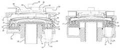
- an apparatus for treating surfaces of wafer-shaped articlescomprises an outer process chamber 1 , which is preferably made of aluminum coated with PFA (perfluoroalkoxy) resin.
- the chamber in this embodimenthas a main cylindrical wall 10 , a lower part 12 and an upper part 15 . From upper part 15 there extends a narrower cylindrical wall 34 , which is closed by a lid 36 .
- a rotary chuck 30is disposed in the upper part of chamber 1 , and surrounded by the cylindrical wall 34 .
- Rotary chuck 30rotatably supports a wafer W during used of the apparatus.
- the rotary chuck 30incorporates a rotary drive comprising ring gear 38 , which engages and drives a plurality of eccentrically movable gripping members for selectively contacting and releasing the peripheral edge of a wafer W.
- the rotary chuck 30is a ring rotor provided adjacent to the interior surface of the cylindrical wall 34 .
- a stator 32is provided opposite the ring rotor adjacent the outer surface of the cylindrical wall 34 .
- the rotor 30 and stator 34serve as a motor by which the ring rotor 30 (and thereby a supported wafer W) may be rotated through an active magnetic bearing.
- the stator 34can comprise a plurality of electromagnetic coils or windings that may be actively controlled to rotatably drive the rotary chuck 30 through corresponding permanent magnets provided on the rotor.
- Axial and radial bearing of the rotary chuck 30may be accomplished also by active control of the stator or by permanent magnets.
- the rotary chuck 30may be levitated and rotatably driven free from mechanical contact.
- the rotormay be held by a passive bearing where the magnets of the rotor are held by corresponding high-temperature-superconducting magnets (HTS-magnets) that are circumferentially arranged on an outer rotor outside the chamber.
- HTS-magnetshigh-temperature-superconducting magnets
- each magnet of the ring rotoris pinned to its corresponding HTS-magnet of the outer rotor. Therefore the inner rotor makes the same movement as the outer rotor without being physically connected.
- the lid 36has a manifold 42 mounted on its exterior, which supplies a medium inlet 44 that traverses the lid 36 and opens into the chamber above the wafer W. It will be noted that the wafer W in this embodiment hangs downwardly from the rotary chuck 30 , supported by the gripping members 40 , such that fluids supplied through inlet 44 would impinge upon the upwardly facing surface of the wafer W.
- wafer 30is a semiconductor wafer, for example of 300 mm or 450 mm diameter
- the upwardly facing side of wafer Wcould be either the device side or the obverse side of the wafer W, which is determined by how the wafer is positioned on the rotary chuck 30 , which in turn is dictated by the particular process being performed within the chamber 1 .
- the apparatus of FIG. 1further comprises an interior cover 2 , which is movable relative to the process chamber 1 .
- Interior cover 2is shown in FIG. 1 in its first, or open, position, in which the rotary chuck 30 is in communication with the outer cylindrical wall 10 of chamber 1 .
- Cover 2 in this embodimentis generally cup-shaped, comprising a base 20 surrounded by an upstanding cylindrical wall 21 .
- Cover 2furthermore comprises a hollow shaft 22 supporting the base 20 , and traversing the lower wall 14 of the chamber 1 .
- Hollow shaft 22is surrounded by a boss 12 formed in the main chamber 1 , and these elements are connected via a dynamic seal that permits the hollow shaft 22 to be displaced relative to the boss 12 while maintaining a gas-tight seal with the chamber 1 .
- Cover 2preferably comprises a fluid medium inlet 28 traversing the base 20 , so that process fluids and rinsing liquid may be introduced into the chamber onto the downwardly facing surface of wafer W.
- Cover 2furthermore includes a process liquid discharge opening 23 , which opens into a discharge pipe 25 .
- pipe 25is rigidly mounted to base 20 of cover 2 , it traverses the bottom wall 14 of chamber 1 via a dynamic seal 17 so that the pipe may slide axially relative to the bottom wall 14 while maintaining a gas-tight seal.
- An exhaust opening 16traverses the wall 10 of chamber 1 , whereas a separate exhaust opening 46 traverses the lid 36 near the inner surface of rotary chuck 30 .
- Each exhaust openingis connected to suitable exhaust conduits (not shown), which are preferably independently controlled via respective valves and venting devices.
- the position depicted in FIG. 1corresponds to loading or unloading of a wafer W.
- a wafer Wcan be loaded onto the rotary chuck 30 either through the lid 36 , or, more preferably, through a side door (not shown) in the chamber wall 10 .
- the lid 36is in position and when any side door has been closed, the chamber 1 is gas-tight and able to maintain a defined internal pressure.
- the interior cover 2has been moved to its second, or closed, position, which corresponds to processing of a wafer W. That is, after a wafer W is loaded onto rotary chuck 30 , the cover 2 is moved upwardly relative to chamber 1 , by a suitable motor (not shown) acting upon the hollow shaft 22 . The upward movement of the interior cover 2 continues until the deflector member 24 comes into contact with the interior surface of the upper part 15 of chamber 1 .
- the gasket 26 carried by deflector 24seals against the underside of upper part 15
- the gasket 18 carried by the upper part 15seals against the upper surface of deflector 24 .
- processing fluidsmay be directed through medium inlets 44 and/or 28 to a rotating wafer W in order to perform various processes, such as etching, cleaning, rinsing, and any other desired surface treatment of the wafer undergoing processing.
- Provision of the inner chamber 48 within the overall process chamber 1thus enhances the safety of environmentally closed chambers by permitting the gases and liquids used for wafer processing to be better isolated from the exterior environment of the process chamber, and reduces the risk of process gas, chemical fumes, hot vapor such as vaporized isopropyl alcohol, ozone and the like being released to the tool environment.
- FIGS. 3-6show a second embodiment according to the present invention, in which the interior cover 2 is provided with a set of dividers so that separate processing regions can be defined within the inner chamber 48 .
- one or more vertically movable splash guards 37 , 39within the interior cover 2 .
- FIGS. 3-6two circular splash guards 37 and 39 are shown although it will be appreciated that any desired number of splash guards may be provided and are contemplated by this disclosure, the actual number of splash guards depending in part upon the number of different process fluids which are intended to be separately collected.
- the outer splash guard 37is positioned concentrically about the inner splash guard 39 .
- the inner splash guard 39defines an inner process fluid collector within its interior.
- a middle process fluid collectoris defined by an annular region formed between the outer surface of the inner splash guard 39 and the inner surface of the outer splash guard 37 .
- An outer process fluid collectoris defined by an annular region formed between the outer surface of the outer splash guard 37 and the inner surface of the cylindrical wall 21 .
- drains 31 , 33 and 35each extend through the base 20 of the interior cover, and also through the bottom wall 14 of the main chamber 1 .
- the assembly of drains 31 , 33 and 35is associated with bottom wall 14 via a dynamic seal as described above, to permit relative movement of the drain lines and the outer chamber 1 while the interior cover 2 is moved, while maintaining a gas-tight seal.
- Deflector 27 in this embodimentis somewhat elongated to accommodate the upper portions of splash guards 37 and 39 , but is otherwise as described above in connection with the first embodiment.
- Splash guards 37 and 39are moved up and down relative to interior cover 2 by suitable actuators such as pneumatic cylinders, combinations of pneumatic and hydraulic cylinders, linear motors, Bowden wires or the like.
- suitable actuatorssuch as pneumatic cylinders, combinations of pneumatic and hydraulic cylinders, linear motors, Bowden wires or the like.
- the actuators for splash guards 37 and 39are similarly mounted traversing bottom wall 14 via a dynamic seal.
- Each splash guardis independently movable in the vertical direction. Accordingly, each splash guard can selectively be raised and/or lowered relative to the rotary chuck 30 , relative to any other splash guard, and relative to the interior cover 2 , such that excess process fluid emanating from the trailing edge of the rotary chuck 30 is directed toward a selected fluid collector.
- both splash guards 37 and 39are shown in an elevated status, such that, in the working position depicted in FIG. 4 , excess process fluid emanating from the trailing edge of the rotary chuck 30 is directed against the inner surface of the inner splash guard 39 and into the inner fluid collector 31 .
- excess fluid from the surface of a wafer undergoing processingcan be selectively recovered through drain 31 and optionally recycled or reused.
- both splash guards 37 and 39are in their upper lower relative to interior cover 2 , with interior cover 2 being in its second or closed position.
- excess process fluid emanating from the trailing edge of the rotary chuck 30is directed against the inner surface of the cylindrical wall 21 and into the outer fluid collector 35 .
- excess fluid from the surface of a wafer undergoing processingcan be selectively recovered through drain 35 and optionally recycled or reused.
- splash guard 39is in its lower position while splash guard 37 is in its upper position relative to interior cover 2 , with interior cover 2 being in its second or closed position.
- excess process fluid emanating from the trailing edge of the rotary chuck 30is directed against the inner surface of the outer splash guard 37 and into the middle fluid collector 33 .
- excess fluid from the surface of a wafer undergoing processingcan be selectively recovered through drain 33 and optionally recycled or reused.
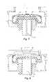
- FIGS. 7 and 8show a third embodiment of the present invention, in which the chamber design of the first embodiment is adapted for use with a spin chuck in which a wafer W is mounted on an upper side of a chuck that is rotated through the action of a motor on a central shaft.
- wafer Wis loaded onto spin chuck 50 when interior cover 2 is in the loading/unloading position depicted in FIG. 7 , and wafer W is secured in the predetermined orientation relative to chuck 50 by gripping members 40 .
- Interior cover 2is then moved to its second position, as described above in connection with the first embodiment, to define the inner chamber 48 .
- spin chuck 50is also vertically moveable relative to the interior cover 2 , so that it can be raised to an optimum processing position within the chamber 48 .
- Spin chuck 50is then rotated by a motor (not shown) acting upon shaft 55 .
- FIGS. 9 and 10show a fourth embodiment of the present invention, in which the spin chuck 50 of the preceding embodiment rotates relative to interior cover 2 , but does not move axially relative to the interior cover 2 .
- wafer Wis loaded onto spin chuck 50 with interior cover 2 is in the loading/unloading position depicted in FIG. 9 , and wafer W is secured in the predetermined orientation relative to chuck 50 by gripping members 40 .
- Interior cover 2is then moved to its second position as depicted in FIG. 10 and as described above in connection with the first embodiment, to define the inner chamber 48 .
- the spin chuck 50 of this embodimentis not vertically moveable relative to the interior cover 2 , the movement of the interior cover 2 serves simultaneously to position wafer W at its final processing position within the chamber 48 .
- Spin chuck 50is then rotated by a motor (not shown) acting upon shaft 55 .
Landscapes
- Engineering & Computer Science (AREA)
- Microelectronics & Electronic Packaging (AREA)
- Condensed Matter Physics & Semiconductors (AREA)
- General Physics & Mathematics (AREA)
- Manufacturing & Machinery (AREA)
- Computer Hardware Design (AREA)
- Physics & Mathematics (AREA)
- Power Engineering (AREA)
- Cleaning Or Drying Semiconductors (AREA)
- Container, Conveyance, Adherence, Positioning, Of Wafer (AREA)
- Magnetic Bearings And Hydrostatic Bearings (AREA)
- Drying Of Semiconductors (AREA)
- Weting (AREA)
Abstract
Description
1. Field of the Invention
The invention relates generally to an apparatus for treating surfaces of wafer-shaped articles, such as semiconductor wafers, wherein one or more treatment fluids may be recovered from within a closed process chamber.
2. Description of Related Art
Semiconductor wafers are subjected to various surface treatment processes such as etching, cleaning, polishing and material deposition. To accommodate such processes, a single wafer may be supported in relation to one or more treatment fluid nozzles by a chuck associated with a rotatable carrier, as is described for example in U.S. Pat. Nos. 4,903,717 and 5,513,668.
Alternatively, a chuck in the form of a ring rotor adapted to support a wafer may be located within a closed process chamber and driven without physical contact through an active magnetic bearing, as is described for example in International Publication No. WO 2007/101764 and U.S. Pat. No. 6,485,531. Treatment fluids which are driven outwardly from the edge of a rotating wafer due to centrifugal action are delivered to a common drain for disposal.
Although conventional closed process chambers adequately contain the hazardous substances used for wafer processing while the chamber is closed, they must be opened for loading and unloading of wafers. This causes a significant risk that process gas, chemical fumes, hot vapor such as vaporized isopropyl alcohol, ozone and the like could be released to the tool environment, which could result in significant safety risks and damage to surrounding components and tools.
The present inventors have developed an improved closed process chamber for treating wafer-shaped articles, in which an inner chamber is provided within an outer chamber, with each of the inner and outer chambers being configured to provide a gas-tight enclosure.
Thus, the invention in one aspect relates to a device for processing wafer-shaped articles, comprising a closed process chamber. The closed process chamber comprises a housing providing a gas-tight enclosure, a rotary chuck located within the closed process chamber and adapted to hold a wafer shaped article thereon, and an interior cover disposed within said closed process chamber. The interior cover is movable between a first position in which the rotary chuck communicates with an outer wall of the closed process chamber, and a second position in which the interior cover seals against an inner surface of the closed process chamber adjacent the rotary chuck to define a gas-tight inner process chamber. Preferably said movement between the first position and the second position is an axial movement along the rotational axis of rotary chuck.
In preferred embodiments of the device according to the present invention, the interior cover forms a lower portion of the inner process chamber when in the second position.
In preferred embodiments of the device according to the present invention, the interior cover comprises a base and at least one upstanding wall, the base being connected to a shaft that penetrates the closed process chamber via a seal that permits relative movement between the shaft and the closed process chamber while maintaining gas tightness of the outer process chamber. Preferably said relative movement is an axial movement along the rotational axis of rotary chuck.
In preferred embodiments of the device according to the present invention, at least one process fluid collector is formed in a lower portion of the interior cover, the process fluid collector communicating with a discharge pipe depending from the interior cover that penetrates the closed process chamber via a seal that permits relative movement between the discharge pipe and the closed process chamber while maintaining gas tightness of the outer process chamber.
In preferred embodiments of the device according to the present invention, the closed process chamber comprises independently controlled exhaust ports, a first exhaust port opening into the closed process chamber in a region inside the inner chamber when the interior cover is in the second position, and a second exhaust port opening into the closed process chamber in a region outside the inner chamber when the interior cover is in the second position.
In preferred embodiments of the device according to the present invention, the interior cover comprises a plurality of splash guards that are independently axially displaceable relative to the interior cover, the splash guards and the interior cover being adapted to define a plurality of distinct processing regions within the inner chamber when the interior cover is in the second position.
In preferred embodiments of the device according to the present invention, each of the distinct processing regions comprises a respective liquid discharge pipe in fluid communication therewith.
In preferred embodiments of the device according to the present invention, each axially displaceable splash guard is selectively driven from outside the closed process chamber to a predefined vertical position.
In preferred embodiments of the device according to the present invention, each axially displaceable splash guard is selectively positionable so as to capture a preselected process fluid emanating from a spinning wafer carried by the rotary chuck.
In preferred embodiments of the device according to the present invention, the rotary chuck is adapted to be driven without physical contact through a magnetic bearing, and the rotary chuck and the interior cover are vertically movable relative to each other.
In preferred embodiments of the device according to the present invention, the magnetic bearing comprises a stator located outside the closed process chamber.
In preferred embodiments of the device according to the present invention, the magnetic bearing is selectively positionable such that a preselected process fluid emanating from a spinning wafer carried by the rotary chuck is directed to a preselected fluid collector.
In preferred embodiments of the device according to the present invention, the magnetic bearing is an active magnetic bearing.
In preferred embodiments of the device according to the present invention, the closed process chamber is a module in a station for single wafer wet processing of semiconductor wafers.
In preferred embodiments of the device according to the present invention, the closed process chamber is made of aluminum coated with perfluoroalkoxy resin.
Other objects, features and advantages of the invention will become more apparent after reading the following detailed description of preferred embodiments of the invention, given with reference to the accompanying drawings, in which:
Referring now toFIG. 1 , an apparatus for treating surfaces of wafer-shaped articles according to a first embodiment of the invention comprises anouter process chamber 1, which is preferably made of aluminum coated with PFA (perfluoroalkoxy) resin. The chamber in this embodiment has a maincylindrical wall 10, alower part 12 and anupper part 15. Fromupper part 15 there extends a narrowercylindrical wall 34, which is closed by alid 36.
Arotary chuck 30 is disposed in the upper part ofchamber 1, and surrounded by thecylindrical wall 34. Rotarychuck 30 rotatably supports a wafer W during used of the apparatus. Therotary chuck 30 incorporates a rotary drive comprisingring gear 38, which engages and drives a plurality of eccentrically movable gripping members for selectively contacting and releasing the peripheral edge of a wafer W.
In this embodiment, therotary chuck 30 is a ring rotor provided adjacent to the interior surface of thecylindrical wall 34. Astator 32 is provided opposite the ring rotor adjacent the outer surface of thecylindrical wall 34. Therotor 30 andstator 34 serve as a motor by which the ring rotor30 (and thereby a supported wafer W) may be rotated through an active magnetic bearing. For example, thestator 34 can comprise a plurality of electromagnetic coils or windings that may be actively controlled to rotatably drive therotary chuck 30 through corresponding permanent magnets provided on the rotor. Axial and radial bearing of therotary chuck 30 may be accomplished also by active control of the stator or by permanent magnets. Thus, therotary chuck 30 may be levitated and rotatably driven free from mechanical contact. Alternatively, the rotor may be held by a passive bearing where the magnets of the rotor are held by corresponding high-temperature-superconducting magnets (HTS-magnets) that are circumferentially arranged on an outer rotor outside the chamber. With this alternative embodiment each magnet of the ring rotor is pinned to its corresponding HTS-magnet of the outer rotor. Therefore the inner rotor makes the same movement as the outer rotor without being physically connected.
Thelid 36 has a manifold42 mounted on its exterior, which supplies amedium inlet 44 that traverses thelid 36 and opens into the chamber above the wafer W. It will be noted that the wafer W in this embodiment hangs downwardly from therotary chuck 30, supported by the grippingmembers 40, such that fluids supplied throughinlet 44 would impinge upon the upwardly facing surface of the wafer W.
Incase wafer 30 is a semiconductor wafer, for example of 300 mm or 450 mm diameter, the upwardly facing side of wafer W could be either the device side or the obverse side of the wafer W, which is determined by how the wafer is positioned on therotary chuck 30, which in turn is dictated by the particular process being performed within thechamber 1.
The apparatus ofFIG. 1 further comprises aninterior cover 2, which is movable relative to theprocess chamber 1.Interior cover 2 is shown inFIG. 1 in its first, or open, position, in which therotary chuck 30 is in communication with the outercylindrical wall 10 ofchamber 1.Cover 2 in this embodiment is generally cup-shaped, comprising a base20 surrounded by an upstandingcylindrical wall 21.Cover 2 furthermore comprises ahollow shaft 22 supporting thebase 20, and traversing thelower wall 14 of thechamber 1.
At the top ofcylindrical wall 21 there is attached anannular deflector member 24, which carries on its upwardly-facing surface agasket 26.Cover 2 preferably comprises a fluidmedium inlet 28 traversing thebase 20, so that process fluids and rinsing liquid may be introduced into the chamber onto the downwardly facing surface of wafer W.
Anexhaust opening 16 traverses thewall 10 ofchamber 1, whereas aseparate exhaust opening 46 traverses thelid 36 near the inner surface ofrotary chuck 30. Each exhaust opening is connected to suitable exhaust conduits (not shown), which are preferably independently controlled via respective valves and venting devices.
The position depicted inFIG. 1 corresponds to loading or unloading of a wafer W. In particular, a wafer W can be loaded onto therotary chuck 30 either through thelid 36, or, more preferably, through a side door (not shown) in thechamber wall 10. However, when thelid 36 is in position and when any side door has been closed, thechamber 1 is gas-tight and able to maintain a defined internal pressure.
InFIG. 2 , theinterior cover 2 has been moved to its second, or closed, position, which corresponds to processing of a wafer W. That is, after a wafer W is loaded ontorotary chuck 30, thecover 2 is moved upwardly relative tochamber 1, by a suitable motor (not shown) acting upon thehollow shaft 22. The upward movement of theinterior cover 2 continues until thedeflector member 24 comes into contact with the interior surface of theupper part 15 ofchamber 1. In particular, thegasket 26 carried bydeflector 24 seals against the underside ofupper part 15, whereas thegasket 18 carried by theupper part 15 seals against the upper surface ofdeflector 24.
When theinterior cover 2 reaches its second position as depicted inFIG. 2 , there is thus created asecond chamber 48 within theclosed process chamber 1.Inner chamber 48 is moreover sealed in a gas tight manner from the remainder of thechamber 1. Moreover, thechamber 48 is preferably separately vented from the remainder ofchamber 1, which is achieved in this embodiment by the provision of theexhaust port 46 opening into thechamber 48, independently from theexhaust port 16 that serves thechamber 1 in general, and the remainder of thechamber 1 in theFIG. 2 configuration.
During processing of a wafer, processing fluids may be directed throughmedium inlets 44 and/or28 to a rotating wafer W in order to perform various processes, such as etching, cleaning, rinsing, and any other desired surface treatment of the wafer undergoing processing.
Provision of theinner chamber 48 within theoverall process chamber 1 thus enhances the safety of environmentally closed chambers by permitting the gases and liquids used for wafer processing to be better isolated from the exterior environment of the process chamber, and reduces the risk of process gas, chemical fumes, hot vapor such as vaporized isopropyl alcohol, ozone and the like being released to the tool environment.
Theouter splash guard 37 is positioned concentrically about theinner splash guard 39. Thus, theinner splash guard 39 defines an inner process fluid collector within its interior. A middle process fluid collector is defined by an annular region formed between the outer surface of theinner splash guard 39 and the inner surface of theouter splash guard 37. An outer process fluid collector is defined by an annular region formed between the outer surface of theouter splash guard 37 and the inner surface of thecylindrical wall 21.
Associated with each such fluid collector a drain is provided for delivering collected process media from the respective fluid collector to outside the closed process chamber. As shown inFIG. 3 , drains31,33 and35 each extend through thebase 20 of the interior cover, and also through thebottom wall 14 of themain chamber 1. The assembly ofdrains bottom wall 14 via a dynamic seal as described above, to permit relative movement of the drain lines and theouter chamber 1 while theinterior cover 2 is moved, while maintaining a gas-tight seal.
Splash guards37 and39 are moved up and down relative tointerior cover 2 by suitable actuators such as pneumatic cylinders, combinations of pneumatic and hydraulic cylinders, linear motors, Bowden wires or the like. Although not shown in the accompanying drawings, the actuators forsplash guards bottom wall 14 via a dynamic seal.
Each splash guard is independently movable in the vertical direction. Accordingly, each splash guard can selectively be raised and/or lowered relative to therotary chuck 30, relative to any other splash guard, and relative to theinterior cover 2, such that excess process fluid emanating from the trailing edge of therotary chuck 30 is directed toward a selected fluid collector.
InFIGS. 3 and 4 , bothsplash guards FIG. 4 , excess process fluid emanating from the trailing edge of therotary chuck 30 is directed against the inner surface of theinner splash guard 39 and into theinner fluid collector 31. Thus, excess fluid from the surface of a wafer undergoing processing can be selectively recovered throughdrain 31 and optionally recycled or reused.
InFIG. 5 , bothsplash guards interior cover 2, withinterior cover 2 being in its second or closed position. In this configuration, excess process fluid emanating from the trailing edge of therotary chuck 30 is directed against the inner surface of thecylindrical wall 21 and into theouter fluid collector 35. Thus, excess fluid from the surface of a wafer undergoing processing can be selectively recovered throughdrain 35 and optionally recycled or reused.
InFIG. 6 ,splash guard 39 is in its lower position whilesplash guard 37 is in its upper position relative tointerior cover 2, withinterior cover 2 being in its second or closed position. In this configuration, excess process fluid emanating from the trailing edge of therotary chuck 30 is directed against the inner surface of theouter splash guard 37 and into themiddle fluid collector 33. Thus, excess fluid from the surface of a wafer undergoing processing can be selectively recovered throughdrain 33 and optionally recycled or reused.
In particular, wafer W is loaded ontospin chuck 50 wheninterior cover 2 is in the loading/unloading position depicted inFIG. 7 , and wafer W is secured in the predetermined orientation relative to chuck50 by grippingmembers 40.Interior cover 2 is then moved to its second position, as described above in connection with the first embodiment, to define theinner chamber 48.
In this embodiment, it will be seen thatspin chuck 50 is also vertically moveable relative to theinterior cover 2, so that it can be raised to an optimum processing position within thechamber 48.Spin chuck 50 is then rotated by a motor (not shown) acting uponshaft 55.
Thus, wafer W is loaded ontospin chuck 50 withinterior cover 2 is in the loading/unloading position depicted inFIG. 9 , and wafer W is secured in the predetermined orientation relative to chuck50 by grippingmembers 40.Interior cover 2 is then moved to its second position as depicted inFIG. 10 and as described above in connection with the first embodiment, to define theinner chamber 48.
As thespin chuck 50 of this embodiment is not vertically moveable relative to theinterior cover 2, the movement of theinterior cover 2 serves simultaneously to position wafer W at its final processing position within thechamber 48.Spin chuck 50 is then rotated by a motor (not shown) acting uponshaft 55.
Claims (19)
1. A device for processing wafer-shaped articles, comprising:
an upper chamber structure that surrounds and supports a rotary chuck, said rotary chuck being adapted to hold a wafer shaped article thereon; and
a cover disposed beneath said upper chamber structure and said rotary chuck, said cover comprising at least one drainage channel and a liquid outlet communicating with said at least one drainage channel,
said cover being movable relative to said upper chamber structure and said rotary chuck between:
a first position in which an annular deflector member that extends upwardly above said at least one drainage channel does not seal against a facing surface of said upper chamber structure adjacent said rotary chuck, and
a second position in which said annular deflector member seals against an inner surface of said upper chamber structure adjacent said rotary chuck to define a gas-tight process chamber.
2. The device according toclaim 1 , wherein said cover comprises a base and at least one upstanding wall, said base being connected to a shaft that penetrates said cover via a seal that permits relative movement between said shaft and said cover while maintaining gas tightness of said gas-tight process chamber.
3. The device according toclaim 2 , further comprising a fluid medium inlet traversing the base of the cover, so that process fluids may be introduced into the gas-tight chamber onto a downwardly facing surface of a wafer.
4. The device according toclaim 1 , wherein said cover comprises a plurality of splash guards that are independently axially displaceable relative to said cover, said splash guards and said cover being adapted to define a plurality of distinct processing regions within said gas-tight chamber when said cover is in said second position.
5. The device according toclaim 4 , wherein each of said distinct processing regions comprises a respective liquid discharge pipe in fluid communication therewith.
6. The device according toclaim 4 , wherein each axially displaceable splash guard is selectively driven from outside the gas-tight process chamber to a predefined vertical position.
7. The device according toclaim 4 , wherein each axially displaceable splash guard is selectively positionable so as to capture a preselected process fluid emanating from a spinning wafer carried by said rotary chuck.
8. The device according toclaim 1 , wherein said rotary chuck is adapted to be driven without physical contact through a magnetic bearing, and wherein said rotary chuck and said cover are vertically movable relative to each other.
9. The device according toclaim 8 , wherein said magnetic bearing comprises a stator located outside the gas-tight process chamber.
10. The device according toclaim 1 , further comprising a pipe connecting said at least one drainage channel and said liquid outlet, said pipe being rigidly mounted to a base of said cover, the pipe traversing a bottom wall of said upper chamber structure via a dynamic seal that allows said pipe to slide axially relative to said bottom wall while maintaining a gas-tight seal when said cover moves between said first and second positions.
11. A device for processing wafer-shaped articles, comprising:
an upper chamber structure that surrounds and supports a rotary chuck, said rotary chuck being adapted to hold a wafer shaped article thereon; and
a cover disposed beneath said upper chamber structure and said rotary chuck, said cover comprising at least one drainage channel and a liquid outlet communicating with said at least one drainage channel,
said cover being mounted for movement between:
a first position in which said cover does not seal against a facing surface of said upper chamber structure adjacent said rotary chuck, and
a second position in which said cover seals against an inner surface of said upper chamber structure adjacent said rotary chuck to define a gas-tight process chamber.
12. The device according toclaim 11 , wherein said cover comprises a base and at least one upstanding wall, said base being connected to a shaft that penetrates said cover via a seal that permits relative movement between said shaft and said cover while maintaining gas tightness of said gas-tight process chamber.
13. The device according toclaim 12 , further comprising a fluid medium inlet traversing the base of the cover, so that process fluids may be introduced into the gas-tight chamber onto a downwardly facing surface of a wafer.
14. The device according toclaim 11 , wherein said cover comprises a plurality of splash guards that are independently axially displaceable relative to said cover, said splash guards and said cover being adapted to define a plurality of distinct processing regions within said gas-tight chamber when said cover is in said second position.
15. The device according toclaim 14 , wherein each of said distinct processing regions comprises a respective liquid discharge pipe in fluid communication therewith.
16. The device according toclaim 14 , wherein each axially displaceable splash guard is selectively driven from outside the gas-tight process chamber to a predefined vertical position.
17. The device according toclaim 14 , wherein each axially displaceable splash guard is selectively positionable so as to capture a preselected process fluid emanating from a spinning wafer carried by said rotary chuck.
18. The device according toclaim 11 , wherein said rotary chuck is adapted to be driven without physical contact through a magnetic bearing, and wherein said rotary chuck and said cover are vertically movable relative to each other.
19. The device according toclaim 18 , wherein said magnetic bearing comprises a stator located outside the gas-tight process chamber.
Priority Applications (1)
| Application Number | Priority Date | Filing Date | Title |
|---|---|---|---|
| US14/871,927US10056287B2 (en) | 2011-09-09 | 2015-09-30 | Apparatus for treating surfaces of wafer-shaped articles |
Applications Claiming Priority (2)
| Application Number | Priority Date | Filing Date | Title |
|---|---|---|---|
| US13/228,980US10269615B2 (en) | 2011-09-09 | 2011-09-09 | Apparatus for treating surfaces of wafer-shaped articles |
| US14/871,927US10056287B2 (en) | 2011-09-09 | 2015-09-30 | Apparatus for treating surfaces of wafer-shaped articles |
Related Parent Applications (1)
| Application Number | Title | Priority Date | Filing Date |
|---|---|---|---|
| US13/228,980DivisionUS10269615B2 (en) | 2011-09-09 | 2011-09-09 | Apparatus for treating surfaces of wafer-shaped articles |
Publications (2)
| Publication Number | Publication Date |
|---|---|
| US20160027680A1 US20160027680A1 (en) | 2016-01-28 |
| US10056287B2true US10056287B2 (en) | 2018-08-21 |
Family
ID=47829153
Family Applications (2)
| Application Number | Title | Priority Date | Filing Date |
|---|---|---|---|
| US13/228,980Active2036-03-16US10269615B2 (en) | 2011-09-09 | 2011-09-09 | Apparatus for treating surfaces of wafer-shaped articles |
| US14/871,927ActiveUS10056287B2 (en) | 2011-09-09 | 2015-09-30 | Apparatus for treating surfaces of wafer-shaped articles |
Family Applications Before (1)
| Application Number | Title | Priority Date | Filing Date |
|---|---|---|---|
| US13/228,980Active2036-03-16US10269615B2 (en) | 2011-09-09 | 2011-09-09 | Apparatus for treating surfaces of wafer-shaped articles |
Country Status (7)
| Country | Link |
|---|---|
| US (2) | US10269615B2 (en) |
| JP (1) | JP6121424B2 (en) |
| KR (1) | KR101986395B1 (en) |
| CN (1) | CN104160496B (en) |
| SG (2) | SG11201400404PA (en) |
| TW (1) | TWI636522B (en) |
| WO (1) | WO2013035019A2 (en) |
Families Citing this family (272)
| Publication number | Priority date | Publication date | Assignee | Title |
|---|---|---|---|---|
| US20130023129A1 (en) | 2011-07-20 | 2013-01-24 | Asm America, Inc. | Pressure transmitter for a semiconductor processing environment |
| US9633890B2 (en)* | 2011-12-16 | 2017-04-25 | Lam Research Ag | Device for treating surfaces of wafer-shaped articles and gripping pin for use in the device |
| JP5973731B2 (en) | 2012-01-13 | 2016-08-23 | 東京エレクトロン株式会社 | Plasma processing apparatus and heater temperature control method |
| KR101501362B1 (en) | 2012-08-09 | 2015-03-10 | 가부시키가이샤 스크린 홀딩스 | Substrate processing apparatus and substrate processing method |
| KR101512560B1 (en) | 2012-08-31 | 2015-04-15 | 가부시키가이샤 스크린 홀딩스 | Substrate processing apparatus |
| US10714315B2 (en) | 2012-10-12 | 2020-07-14 | Asm Ip Holdings B.V. | Semiconductor reaction chamber showerhead |
| US20160376700A1 (en) | 2013-02-01 | 2016-12-29 | Asm Ip Holding B.V. | System for treatment of deposition reactor |
| US20140283994A1 (en)* | 2013-03-22 | 2014-09-25 | Lam Research Ag | Apparatus for treating surfaces of wafer-shaped articles |
| US9597701B2 (en) | 2013-12-31 | 2017-03-21 | Lam Research Ag | Apparatus for treating surfaces of wafer-shaped articles |
| US10043686B2 (en)* | 2013-12-31 | 2018-08-07 | Lam Research Ag | Apparatus for treating surfaces of wafer-shaped articles |
| US9657397B2 (en) | 2013-12-31 | 2017-05-23 | Lam Research Ag | Apparatus for treating surfaces of wafer-shaped articles |
| WO2015162194A1 (en)* | 2014-04-24 | 2015-10-29 | Struers A/S | A method of, and an apparatus for, rinsing materialographic samples |
| KR102255792B1 (en) | 2014-06-26 | 2021-05-27 | 주식회사 만도 | Pedal simulator |
| US10941490B2 (en) | 2014-10-07 | 2021-03-09 | Asm Ip Holding B.V. | Multiple temperature range susceptor, assembly, reactor and system including the susceptor, and methods of using the same |
| US10167552B2 (en)* | 2015-02-05 | 2019-01-01 | Lam Research Ag | Spin chuck with rotating gas showerhead |
| US10276355B2 (en) | 2015-03-12 | 2019-04-30 | Asm Ip Holding B.V. | Multi-zone reactor, system including the reactor, and method of using the same |
| US10458018B2 (en) | 2015-06-26 | 2019-10-29 | Asm Ip Holding B.V. | Structures including metal carbide material, devices including the structures, and methods of forming same |
| US10014198B2 (en)* | 2015-08-21 | 2018-07-03 | Lam Research Corporation | Wear detection of consumable part in semiconductor manufacturing equipment |
| US10211308B2 (en) | 2015-10-21 | 2019-02-19 | Asm Ip Holding B.V. | NbMC layers |
| US9887120B2 (en)* | 2015-11-03 | 2018-02-06 | Lam Research Ag | Apparatus for treating surfaces of wafer-shaped articles |
| US11139308B2 (en) | 2015-12-29 | 2021-10-05 | Asm Ip Holding B.V. | Atomic layer deposition of III-V compounds to form V-NAND devices |
| US10529554B2 (en) | 2016-02-19 | 2020-01-07 | Asm Ip Holding B.V. | Method for forming silicon nitride film selectively on sidewalls or flat surfaces of trenches |
| TW201731600A (en)* | 2016-03-02 | 2017-09-16 | Els System Technology Co Ltd | Anti splash device of wafer cleaning machine having a mask unit to switch between a folded status and an unfolded status relative to the wafer bearing device |
| US10249521B2 (en) | 2016-03-17 | 2019-04-02 | Lam Research Ag | Wet-dry integrated wafer processing system |
| US10343920B2 (en) | 2016-03-18 | 2019-07-09 | Asm Ip Holding B.V. | Aligned carbon nanotubes |
| US11453943B2 (en) | 2016-05-25 | 2022-09-27 | Asm Ip Holding B.V. | Method for forming carbon-containing silicon/metal oxide or nitride film by ALD using silicon precursor and hydrocarbon precursor |
| US10612137B2 (en) | 2016-07-08 | 2020-04-07 | Asm Ip Holdings B.V. | Organic reactants for atomic layer deposition |
| US9859151B1 (en) | 2016-07-08 | 2018-01-02 | Asm Ip Holding B.V. | Selective film deposition method to form air gaps |
| US9887082B1 (en) | 2016-07-28 | 2018-02-06 | Asm Ip Holding B.V. | Method and apparatus for filling a gap |
| US9812320B1 (en) | 2016-07-28 | 2017-11-07 | Asm Ip Holding B.V. | Method and apparatus for filling a gap |
| US11532757B2 (en) | 2016-10-27 | 2022-12-20 | Asm Ip Holding B.V. | Deposition of charge trapping layers |
| US10714350B2 (en) | 2016-11-01 | 2020-07-14 | ASM IP Holdings, B.V. | Methods for forming a transition metal niobium nitride film on a substrate by atomic layer deposition and related semiconductor device structures |
| CN109923659B (en)* | 2016-11-09 | 2024-03-12 | 东京毅力科创Fsi公司 | Magnetically levitated and rotating chuck for processing microelectronic substrates in a processing chamber |
| TWI645913B (en)* | 2016-11-10 | 2019-01-01 | 辛耘企業股份有限公司 | Liquid processing device |
| KR102546317B1 (en) | 2016-11-15 | 2023-06-21 | 에이에스엠 아이피 홀딩 비.브이. | Gas supply unit and substrate processing apparatus including the same |
| TWI765936B (en) | 2016-11-29 | 2022-06-01 | 美商東京威力科創Fsi股份有限公司 | Translating and rotating chuck for processing microelectronic substrates in a process chamber |
| KR102762543B1 (en) | 2016-12-14 | 2025-02-05 | 에이에스엠 아이피 홀딩 비.브이. | Substrate processing apparatus |
| US11581186B2 (en) | 2016-12-15 | 2023-02-14 | Asm Ip Holding B.V. | Sequential infiltration synthesis apparatus |
| US11447861B2 (en) | 2016-12-15 | 2022-09-20 | Asm Ip Holding B.V. | Sequential infiltration synthesis apparatus and a method of forming a patterned structure |
| US10269558B2 (en) | 2016-12-22 | 2019-04-23 | Asm Ip Holding B.V. | Method of forming a structure on a substrate |
| US11390950B2 (en) | 2017-01-10 | 2022-07-19 | Asm Ip Holding B.V. | Reactor system and method to reduce residue buildup during a film deposition process |
| KR102493551B1 (en) | 2017-01-27 | 2023-01-30 | 티이엘 매뉴팩처링 앤드 엔지니어링 오브 아메리카, 인크. | Systems and methods for rotating and translating a substrate in a process chamber |
| US10468261B2 (en) | 2017-02-15 | 2019-11-05 | Asm Ip Holding B.V. | Methods for forming a metallic film on a substrate by cyclical deposition and related semiconductor device structures |
| WO2018161205A1 (en)* | 2017-03-06 | 2018-09-13 | Acm Research (Shanghai) Inc. | Apparatus for cleaning semiconductor substrates |
| US10770286B2 (en) | 2017-05-08 | 2020-09-08 | Asm Ip Holdings B.V. | Methods for selectively forming a silicon nitride film on a substrate and related semiconductor device structures |
| US12040200B2 (en) | 2017-06-20 | 2024-07-16 | Asm Ip Holding B.V. | Semiconductor processing apparatus and methods for calibrating a semiconductor processing apparatus |
| US11306395B2 (en) | 2017-06-28 | 2022-04-19 | Asm Ip Holding B.V. | Methods for depositing a transition metal nitride film on a substrate by atomic layer deposition and related deposition apparatus |
| KR20190009245A (en) | 2017-07-18 | 2019-01-28 | 에이에스엠 아이피 홀딩 비.브이. | Methods for forming a semiconductor device structure and related semiconductor device structures |
| US11374112B2 (en) | 2017-07-19 | 2022-06-28 | Asm Ip Holding B.V. | Method for depositing a group IV semiconductor and related semiconductor device structures |
| US10590535B2 (en)* | 2017-07-26 | 2020-03-17 | Asm Ip Holdings B.V. | Chemical treatment, deposition and/or infiltration apparatus and method for using the same |
| TWI815813B (en) | 2017-08-04 | 2023-09-21 | 荷蘭商Asm智慧財產控股公司 | Showerhead assembly for distributing a gas within a reaction chamber |
| US10692741B2 (en) | 2017-08-08 | 2020-06-23 | Asm Ip Holdings B.V. | Radiation shield |
| US10770336B2 (en) | 2017-08-08 | 2020-09-08 | Asm Ip Holding B.V. | Substrate lift mechanism and reactor including same |
| US11769682B2 (en) | 2017-08-09 | 2023-09-26 | Asm Ip Holding B.V. | Storage apparatus for storing cassettes for substrates and processing apparatus equipped therewith |
| US11830730B2 (en) | 2017-08-29 | 2023-11-28 | Asm Ip Holding B.V. | Layer forming method and apparatus |
| US11295980B2 (en) | 2017-08-30 | 2022-04-05 | Asm Ip Holding B.V. | Methods for depositing a molybdenum metal film over a dielectric surface of a substrate by a cyclical deposition process and related semiconductor device structures |
| US10658205B2 (en) | 2017-09-28 | 2020-05-19 | Asm Ip Holdings B.V. | Chemical dispensing apparatus and methods for dispensing a chemical to a reaction chamber |
| US10403504B2 (en) | 2017-10-05 | 2019-09-03 | Asm Ip Holding B.V. | Method for selectively depositing a metallic film on a substrate |
| US10923344B2 (en) | 2017-10-30 | 2021-02-16 | Asm Ip Holding B.V. | Methods for forming a semiconductor structure and related semiconductor structures |
| CN111344522B (en) | 2017-11-27 | 2022-04-12 | 阿斯莫Ip控股公司 | Including clean mini-environment device |
| WO2019103613A1 (en) | 2017-11-27 | 2019-05-31 | Asm Ip Holding B.V. | A storage device for storing wafer cassettes for use with a batch furnace |
| US10872771B2 (en) | 2018-01-16 | 2020-12-22 | Asm Ip Holding B. V. | Method for depositing a material film on a substrate within a reaction chamber by a cyclical deposition process and related device structures |
| TWI799494B (en) | 2018-01-19 | 2023-04-21 | 荷蘭商Asm 智慧財產控股公司 | Deposition method |
| KR102695659B1 (en) | 2018-01-19 | 2024-08-14 | 에이에스엠 아이피 홀딩 비.브이. | Method for depositing a gap filling layer by plasma assisted deposition |
| US11081345B2 (en) | 2018-02-06 | 2021-08-03 | Asm Ip Holding B.V. | Method of post-deposition treatment for silicon oxide film |
| WO2019158960A1 (en) | 2018-02-14 | 2019-08-22 | Asm Ip Holding B.V. | A method for depositing a ruthenium-containing film on a substrate by a cyclical deposition process |
| US10896820B2 (en) | 2018-02-14 | 2021-01-19 | Asm Ip Holding B.V. | Method for depositing a ruthenium-containing film on a substrate by a cyclical deposition process |
| US10731249B2 (en) | 2018-02-15 | 2020-08-04 | Asm Ip Holding B.V. | Method of forming a transition metal containing film on a substrate by a cyclical deposition process, a method for supplying a transition metal halide compound to a reaction chamber, and related vapor deposition apparatus |
| JP7357625B2 (en) | 2018-02-19 | 2023-10-06 | ティーイーエル マニュファクチュアリング アンド エンジニアリング オブ アメリカ,インコーポレイテッド | Compact electronic processing system with controllable beam size processing spray |
| KR102636427B1 (en) | 2018-02-20 | 2024-02-13 | 에이에스엠 아이피 홀딩 비.브이. | Substrate processing method and apparatus |
| US10975470B2 (en) | 2018-02-23 | 2021-04-13 | Asm Ip Holding B.V. | Apparatus for detecting or monitoring for a chemical precursor in a high temperature environment |
| US11473195B2 (en) | 2018-03-01 | 2022-10-18 | Asm Ip Holding B.V. | Semiconductor processing apparatus and a method for processing a substrate |
| US11629406B2 (en) | 2018-03-09 | 2023-04-18 | Asm Ip Holding B.V. | Semiconductor processing apparatus comprising one or more pyrometers for measuring a temperature of a substrate during transfer of the substrate |
| KR102646467B1 (en) | 2018-03-27 | 2024-03-11 | 에이에스엠 아이피 홀딩 비.브이. | Method of forming an electrode on a substrate and a semiconductor device structure including an electrode |
| US11230766B2 (en) | 2018-03-29 | 2022-01-25 | Asm Ip Holding B.V. | Substrate processing apparatus and method |
| KR102600229B1 (en) | 2018-04-09 | 2023-11-10 | 에이에스엠 아이피 홀딩 비.브이. | Substrate supporting device, substrate processing apparatus including the same and substrate processing method |
| US12025484B2 (en) | 2018-05-08 | 2024-07-02 | Asm Ip Holding B.V. | Thin film forming method |
| TWI811348B (en) | 2018-05-08 | 2023-08-11 | 荷蘭商Asm 智慧財產控股公司 | Methods for depositing an oxide film on a substrate by a cyclical deposition process and related device structures |
| US12272527B2 (en) | 2018-05-09 | 2025-04-08 | Asm Ip Holding B.V. | Apparatus for use with hydrogen radicals and method of using same |
| KR102596988B1 (en) | 2018-05-28 | 2023-10-31 | 에이에스엠 아이피 홀딩 비.브이. | Method of processing a substrate and a device manufactured by the same |
| TWI840362B (en) | 2018-06-04 | 2024-05-01 | 荷蘭商Asm Ip私人控股有限公司 | Wafer handling chamber with moisture reduction |
| US11718913B2 (en) | 2018-06-04 | 2023-08-08 | Asm Ip Holding B.V. | Gas distribution system and reactor system including same |
| US11286562B2 (en) | 2018-06-08 | 2022-03-29 | Asm Ip Holding B.V. | Gas-phase chemical reactor and method of using same |
| KR102568797B1 (en) | 2018-06-21 | 2023-08-21 | 에이에스엠 아이피 홀딩 비.브이. | Substrate processing system |
| US10797133B2 (en) | 2018-06-21 | 2020-10-06 | Asm Ip Holding B.V. | Method for depositing a phosphorus doped silicon arsenide film and related semiconductor device structures |
| TWI873894B (en) | 2018-06-27 | 2025-02-21 | 荷蘭商Asm Ip私人控股有限公司 | Cyclic deposition methods for forming metal-containing material and films and structures including the metal-containing material |
| KR102854019B1 (en) | 2018-06-27 | 2025-09-02 | 에이에스엠 아이피 홀딩 비.브이. | Periodic deposition method for forming a metal-containing material and films and structures comprising the metal-containing material |
| US10612136B2 (en) | 2018-06-29 | 2020-04-07 | ASM IP Holding, B.V. | Temperature-controlled flange and reactor system including same |
| US10755922B2 (en) | 2018-07-03 | 2020-08-25 | Asm Ip Holding B.V. | Method for depositing silicon-free carbon-containing film as gap-fill layer by pulse plasma-assisted deposition |
| US10388513B1 (en) | 2018-07-03 | 2019-08-20 | Asm Ip Holding B.V. | Method for depositing silicon-free carbon-containing film as gap-fill layer by pulse plasma-assisted deposition |
| US11545387B2 (en) | 2018-07-13 | 2023-01-03 | Tel Manufacturing And Engineering Of America, Inc. | Magnetic integrated lift pin system for a chemical processing chamber |
| US11430674B2 (en) | 2018-08-22 | 2022-08-30 | Asm Ip Holding B.V. | Sensor array, apparatus for dispensing a vapor phase reactant to a reaction chamber and related methods |
| US11024523B2 (en) | 2018-09-11 | 2021-06-01 | Asm Ip Holding B.V. | Substrate processing apparatus and method |
| KR102707956B1 (en) | 2018-09-11 | 2024-09-19 | 에이에스엠 아이피 홀딩 비.브이. | Method for deposition of a thin film |
| CN110970344B (en) | 2018-10-01 | 2024-10-25 | Asmip控股有限公司 | Substrate holding apparatus, system comprising the same and method of using the same |
| US11232963B2 (en) | 2018-10-03 | 2022-01-25 | Asm Ip Holding B.V. | Substrate processing apparatus and method |
| KR102592699B1 (en) | 2018-10-08 | 2023-10-23 | 에이에스엠 아이피 홀딩 비.브이. | Substrate support unit and apparatuses for depositing thin film and processing the substrate including the same |
| KR102546322B1 (en) | 2018-10-19 | 2023-06-21 | 에이에스엠 아이피 홀딩 비.브이. | Substrate processing apparatus and substrate processing method |
| KR102605121B1 (en) | 2018-10-19 | 2023-11-23 | 에이에스엠 아이피 홀딩 비.브이. | Substrate processing apparatus and substrate processing method |
| US12378665B2 (en) | 2018-10-26 | 2025-08-05 | Asm Ip Holding B.V. | High temperature coatings for a preclean and etch apparatus and related methods |
| US11087997B2 (en) | 2018-10-31 | 2021-08-10 | Asm Ip Holding B.V. | Substrate processing apparatus for processing substrates |
| KR102748291B1 (en) | 2018-11-02 | 2024-12-31 | 에이에스엠 아이피 홀딩 비.브이. | Substrate support unit and substrate processing apparatus including the same |
| US11572620B2 (en) | 2018-11-06 | 2023-02-07 | Asm Ip Holding B.V. | Methods for selectively depositing an amorphous silicon film on a substrate |
| US10818758B2 (en) | 2018-11-16 | 2020-10-27 | Asm Ip Holding B.V. | Methods for forming a metal silicate film on a substrate in a reaction chamber and related semiconductor device structures |
| US12040199B2 (en) | 2018-11-28 | 2024-07-16 | Asm Ip Holding B.V. | Substrate processing apparatus for processing substrates |
| US11217444B2 (en) | 2018-11-30 | 2022-01-04 | Asm Ip Holding B.V. | Method for forming an ultraviolet radiation responsive metal oxide-containing film |
| KR102636428B1 (en) | 2018-12-04 | 2024-02-13 | 에이에스엠 아이피 홀딩 비.브이. | A method for cleaning a substrate processing apparatus |
| US11158513B2 (en) | 2018-12-13 | 2021-10-26 | Asm Ip Holding B.V. | Methods for forming a rhenium-containing film on a substrate by a cyclical deposition process and related semiconductor device structures |
| TWI874340B (en) | 2018-12-14 | 2025-03-01 | 荷蘭商Asm Ip私人控股有限公司 | Method of forming device structure, structure formed by the method and system for performing the method |
| TWI866480B (en) | 2019-01-17 | 2024-12-11 | 荷蘭商Asm Ip 私人控股有限公司 | Methods of forming a transition metal containing film on a substrate by a cyclical deposition process |
| KR102727227B1 (en) | 2019-01-22 | 2024-11-07 | 에이에스엠 아이피 홀딩 비.브이. | Semiconductor processing device |
| TWI873122B (en) | 2019-02-20 | 2025-02-21 | 荷蘭商Asm Ip私人控股有限公司 | Method of filling a recess formed within a surface of a substrate, semiconductor structure formed according to the method, and semiconductor processing apparatus |
| TWI838458B (en) | 2019-02-20 | 2024-04-11 | 荷蘭商Asm Ip私人控股有限公司 | Apparatus and methods for plug fill deposition in 3-d nand applications |
| KR102626263B1 (en) | 2019-02-20 | 2024-01-16 | 에이에스엠 아이피 홀딩 비.브이. | Cyclical deposition method including treatment step and apparatus for same |
| TWI845607B (en) | 2019-02-20 | 2024-06-21 | 荷蘭商Asm Ip私人控股有限公司 | Cyclical deposition method and apparatus for filling a recess formed within a substrate surface |
| TWI842826B (en) | 2019-02-22 | 2024-05-21 | 荷蘭商Asm Ip私人控股有限公司 | Substrate processing apparatus and method for processing substrate |
| US11742198B2 (en) | 2019-03-08 | 2023-08-29 | Asm Ip Holding B.V. | Structure including SiOCN layer and method of forming same |
| KR102858005B1 (en) | 2019-03-08 | 2025-09-09 | 에이에스엠 아이피 홀딩 비.브이. | Method for Selective Deposition of Silicon Nitride Layer and Structure Including Selectively-Deposited Silicon Nitride Layer |
| JP2020167398A (en) | 2019-03-28 | 2020-10-08 | エーエスエム・アイピー・ホールディング・ベー・フェー | Door openers and substrate processing equipment provided with door openers |
| KR102809999B1 (en) | 2019-04-01 | 2025-05-19 | 에이에스엠 아이피 홀딩 비.브이. | Method of manufacturing semiconductor device |
| KR20200123380A (en) | 2019-04-19 | 2020-10-29 | 에이에스엠 아이피 홀딩 비.브이. | Layer forming method and apparatus |
| KR20200125453A (en) | 2019-04-24 | 2020-11-04 | 에이에스엠 아이피 홀딩 비.브이. | Gas-phase reactor system and method of using same |
| US11289326B2 (en) | 2019-05-07 | 2022-03-29 | Asm Ip Holding B.V. | Method for reforming amorphous carbon polymer film |
| KR20200130121A (en) | 2019-05-07 | 2020-11-18 | 에이에스엠 아이피 홀딩 비.브이. | Chemical source vessel with dip tube |
| KR20200130652A (en) | 2019-05-10 | 2020-11-19 | 에이에스엠 아이피 홀딩 비.브이. | Method of depositing material onto a surface and structure formed according to the method |
| JP7612342B2 (en) | 2019-05-16 | 2025-01-14 | エーエスエム・アイピー・ホールディング・ベー・フェー | Wafer boat handling apparatus, vertical batch furnace and method |
| JP7598201B2 (en) | 2019-05-16 | 2024-12-11 | エーエスエム・アイピー・ホールディング・ベー・フェー | Wafer boat handling apparatus, vertical batch furnace and method |
| USD975665S1 (en) | 2019-05-17 | 2023-01-17 | Asm Ip Holding B.V. | Susceptor shaft |
| USD947913S1 (en) | 2019-05-17 | 2022-04-05 | Asm Ip Holding B.V. | Susceptor shaft |
| KR20200141002A (en) | 2019-06-06 | 2020-12-17 | 에이에스엠 아이피 홀딩 비.브이. | Method of using a gas-phase reactor system including analyzing exhausted gas |
| KR20200141931A (en) | 2019-06-10 | 2020-12-21 | 에이에스엠 아이피 홀딩 비.브이. | Method for cleaning quartz epitaxial chambers |
| KR20200143254A (en) | 2019-06-11 | 2020-12-23 | 에이에스엠 아이피 홀딩 비.브이. | Method of forming an electronic structure using an reforming gas, system for performing the method, and structure formed using the method |
| USD944946S1 (en) | 2019-06-14 | 2022-03-01 | Asm Ip Holding B.V. | Shower plate |
| KR20210005515A (en) | 2019-07-03 | 2021-01-14 | 에이에스엠 아이피 홀딩 비.브이. | Temperature control assembly for substrate processing apparatus and method of using same |
| JP7499079B2 (en) | 2019-07-09 | 2024-06-13 | エーエスエム・アイピー・ホールディング・ベー・フェー | Plasma device using coaxial waveguide and substrate processing method |
| CN112216646A (en) | 2019-07-10 | 2021-01-12 | Asm Ip私人控股有限公司 | Substrate supporting assembly and substrate processing device comprising same |
| KR20210010307A (en) | 2019-07-16 | 2021-01-27 | 에이에스엠 아이피 홀딩 비.브이. | Substrate processing apparatus |
| KR20210010816A (en) | 2019-07-17 | 2021-01-28 | 에이에스엠 아이피 홀딩 비.브이. | Radical assist ignition plasma system and method |
| KR102860110B1 (en) | 2019-07-17 | 2025-09-16 | 에이에스엠 아이피 홀딩 비.브이. | Methods of forming silicon germanium structures |
| US11643724B2 (en) | 2019-07-18 | 2023-05-09 | Asm Ip Holding B.V. | Method of forming structures using a neutral beam |
| KR20210010817A (en) | 2019-07-19 | 2021-01-28 | 에이에스엠 아이피 홀딩 비.브이. | Method of Forming Topology-Controlled Amorphous Carbon Polymer Film |
| TWI839544B (en) | 2019-07-19 | 2024-04-21 | 荷蘭商Asm Ip私人控股有限公司 | Method of forming topology-controlled amorphous carbon polymer film |
| TWI851767B (en) | 2019-07-29 | 2024-08-11 | 荷蘭商Asm Ip私人控股有限公司 | Methods for selective deposition utilizing n-type dopants and/or alternative dopants to achieve high dopant incorporation |
| US12169361B2 (en) | 2019-07-30 | 2024-12-17 | Asm Ip Holding B.V. | Substrate processing apparatus and method |
| CN112309900A (en) | 2019-07-30 | 2021-02-02 | Asm Ip私人控股有限公司 | Substrate processing apparatus |
| CN112309899A (en) | 2019-07-30 | 2021-02-02 | Asm Ip私人控股有限公司 | Substrate processing apparatus |
| US11587814B2 (en) | 2019-07-31 | 2023-02-21 | Asm Ip Holding B.V. | Vertical batch furnace assembly |
| US11587815B2 (en) | 2019-07-31 | 2023-02-21 | Asm Ip Holding B.V. | Vertical batch furnace assembly |
| US11227782B2 (en) | 2019-07-31 | 2022-01-18 | Asm Ip Holding B.V. | Vertical batch furnace assembly |
| CN112323048B (en) | 2019-08-05 | 2024-02-09 | Asm Ip私人控股有限公司 | Liquid level sensor for chemical source container |
| CN112342526A (en) | 2019-08-09 | 2021-02-09 | Asm Ip私人控股有限公司 | Heater assembly including cooling device and method of using same |
| USD965524S1 (en) | 2019-08-19 | 2022-10-04 | Asm Ip Holding B.V. | Susceptor support |
| USD965044S1 (en) | 2019-08-19 | 2022-09-27 | Asm Ip Holding B.V. | Susceptor shaft |
| JP2021031769A (en) | 2019-08-21 | 2021-03-01 | エーエスエム アイピー ホールディング ビー.ブイ. | Production apparatus of mixed gas of film deposition raw material and film deposition apparatus |
| USD949319S1 (en) | 2019-08-22 | 2022-04-19 | Asm Ip Holding B.V. | Exhaust duct |
| KR20210024423A (en) | 2019-08-22 | 2021-03-05 | 에이에스엠 아이피 홀딩 비.브이. | Method for forming a structure with a hole |
| USD979506S1 (en) | 2019-08-22 | 2023-02-28 | Asm Ip Holding B.V. | Insulator |
| USD940837S1 (en) | 2019-08-22 | 2022-01-11 | Asm Ip Holding B.V. | Electrode |
| KR20210024420A (en) | 2019-08-23 | 2021-03-05 | 에이에스엠 아이피 홀딩 비.브이. | Method for depositing silicon oxide film having improved quality by peald using bis(diethylamino)silane |
| US11286558B2 (en) | 2019-08-23 | 2022-03-29 | Asm Ip Holding B.V. | Methods for depositing a molybdenum nitride film on a surface of a substrate by a cyclical deposition process and related semiconductor device structures including a molybdenum nitride film |
| KR102806450B1 (en) | 2019-09-04 | 2025-05-12 | 에이에스엠 아이피 홀딩 비.브이. | Methods for selective deposition using a sacrificial capping layer |
| KR102733104B1 (en) | 2019-09-05 | 2024-11-22 | 에이에스엠 아이피 홀딩 비.브이. | Substrate processing apparatus |
| US11562901B2 (en) | 2019-09-25 | 2023-01-24 | Asm Ip Holding B.V. | Substrate processing method |
| CN112593212B (en) | 2019-10-02 | 2023-12-22 | Asm Ip私人控股有限公司 | Method for forming topologically selective silicon oxide film by cyclic plasma enhanced deposition process |
| KR20210042810A (en) | 2019-10-08 | 2021-04-20 | 에이에스엠 아이피 홀딩 비.브이. | Reactor system including a gas distribution assembly for use with activated species and method of using same |
| TWI846953B (en) | 2019-10-08 | 2024-07-01 | 荷蘭商Asm Ip私人控股有限公司 | Substrate processing device |
| TW202128273A (en) | 2019-10-08 | 2021-08-01 | 荷蘭商Asm Ip私人控股有限公司 | Gas injection system, reactor system, and method of depositing material on surface of substratewithin reaction chamber |
| TWI846966B (en) | 2019-10-10 | 2024-07-01 | 荷蘭商Asm Ip私人控股有限公司 | Method of forming a photoresist underlayer and structure including same |
| US12009241B2 (en) | 2019-10-14 | 2024-06-11 | Asm Ip Holding B.V. | Vertical batch furnace assembly with detector to detect cassette |
| TWI834919B (en) | 2019-10-16 | 2024-03-11 | 荷蘭商Asm Ip私人控股有限公司 | Method of topology-selective film formation of silicon oxide |
| US11637014B2 (en) | 2019-10-17 | 2023-04-25 | Asm Ip Holding B.V. | Methods for selective deposition of doped semiconductor material |
| KR102845724B1 (en) | 2019-10-21 | 2025-08-13 | 에이에스엠 아이피 홀딩 비.브이. | Apparatus and methods for selectively etching films |
| KR20210050453A (en) | 2019-10-25 | 2021-05-07 | 에이에스엠 아이피 홀딩 비.브이. | Methods for filling a gap feature on a substrate surface and related semiconductor structures |
| US11646205B2 (en) | 2019-10-29 | 2023-05-09 | Asm Ip Holding B.V. | Methods of selectively forming n-type doped material on a surface, systems for selectively forming n-type doped material, and structures formed using same |
| KR20210054983A (en) | 2019-11-05 | 2021-05-14 | 에이에스엠 아이피 홀딩 비.브이. | Structures with doped semiconductor layers and methods and systems for forming same |
| US11501968B2 (en) | 2019-11-15 | 2022-11-15 | Asm Ip Holding B.V. | Method for providing a semiconductor device with silicon filled gaps |
| KR102861314B1 (en) | 2019-11-20 | 2025-09-17 | 에이에스엠 아이피 홀딩 비.브이. | Method of depositing carbon-containing material on a surface of a substrate, structure formed using the method, and system for forming the structure |
| US11450529B2 (en) | 2019-11-26 | 2022-09-20 | Asm Ip Holding B.V. | Methods for selectively forming a target film on a substrate comprising a first dielectric surface and a second metallic surface |
| CN112951697B (en) | 2019-11-26 | 2025-07-29 | Asmip私人控股有限公司 | Substrate processing apparatus |
| CN112885692B (en) | 2019-11-29 | 2025-08-15 | Asmip私人控股有限公司 | Substrate processing apparatus |
| CN120432376A (en) | 2019-11-29 | 2025-08-05 | Asm Ip私人控股有限公司 | Substrate processing apparatus |
| JP7527928B2 (en) | 2019-12-02 | 2024-08-05 | エーエスエム・アイピー・ホールディング・ベー・フェー | Substrate processing apparatus and substrate processing method |
| KR20210070898A (en) | 2019-12-04 | 2021-06-15 | 에이에스엠 아이피 홀딩 비.브이. | Substrate processing apparatus |
| KR20210078405A (en) | 2019-12-17 | 2021-06-28 | 에이에스엠 아이피 홀딩 비.브이. | Method of forming vanadium nitride layer and structure including the vanadium nitride layer |
| KR20210080214A (en) | 2019-12-19 | 2021-06-30 | 에이에스엠 아이피 홀딩 비.브이. | Methods for filling a gap feature on a substrate and related semiconductor structures |
| JP7730637B2 (en) | 2020-01-06 | 2025-08-28 | エーエスエム・アイピー・ホールディング・ベー・フェー | Gas delivery assembly, components thereof, and reactor system including same |
| JP7636892B2 (en) | 2020-01-06 | 2025-02-27 | エーエスエム・アイピー・ホールディング・ベー・フェー | Channeled Lift Pins |
| US11993847B2 (en) | 2020-01-08 | 2024-05-28 | Asm Ip Holding B.V. | Injector |
| KR20210093163A (en) | 2020-01-16 | 2021-07-27 | 에이에스엠 아이피 홀딩 비.브이. | Method of forming high aspect ratio features |
| KR102675856B1 (en) | 2020-01-20 | 2024-06-17 | 에이에스엠 아이피 홀딩 비.브이. | Method of forming thin film and method of modifying surface of thin film |
| TWI889744B (en) | 2020-01-29 | 2025-07-11 | 荷蘭商Asm Ip私人控股有限公司 | Contaminant trap system, and baffle plate stack |
| TW202513845A (en) | 2020-02-03 | 2025-04-01 | 荷蘭商Asm Ip私人控股有限公司 | Semiconductor structures and methods for forming the same |
| KR20210100010A (en) | 2020-02-04 | 2021-08-13 | 에이에스엠 아이피 홀딩 비.브이. | Method and apparatus for transmittance measurements of large articles |
| US11776846B2 (en) | 2020-02-07 | 2023-10-03 | Asm Ip Holding B.V. | Methods for depositing gap filling fluids and related systems and devices |
| TW202146691A (en) | 2020-02-13 | 2021-12-16 | 荷蘭商Asm Ip私人控股有限公司 | Gas distribution assembly, shower plate assembly, and method of adjusting conductance of gas to reaction chamber |
| KR20210103956A (en) | 2020-02-13 | 2021-08-24 | 에이에스엠 아이피 홀딩 비.브이. | Substrate processing apparatus including light receiving device and calibration method of light receiving device |
| TWI855223B (en) | 2020-02-17 | 2024-09-11 | 荷蘭商Asm Ip私人控股有限公司 | Method for growing phosphorous-doped silicon layer |
| CN113410160A (en) | 2020-02-28 | 2021-09-17 | Asm Ip私人控股有限公司 | System specially used for cleaning parts |
| KR20210113043A (en) | 2020-03-04 | 2021-09-15 | 에이에스엠 아이피 홀딩 비.브이. | Alignment fixture for a reactor system |
| US11876356B2 (en) | 2020-03-11 | 2024-01-16 | Asm Ip Holding B.V. | Lockout tagout assembly and system and method of using same |
| KR20210116240A (en) | 2020-03-11 | 2021-09-27 | 에이에스엠 아이피 홀딩 비.브이. | Substrate handling device with adjustable joints |
| KR102775390B1 (en) | 2020-03-12 | 2025-02-28 | 에이에스엠 아이피 홀딩 비.브이. | Method for Fabricating Layer Structure Having Target Topological Profile |
| US12173404B2 (en) | 2020-03-17 | 2024-12-24 | Asm Ip Holding B.V. | Method of depositing epitaxial material, structure formed using the method, and system for performing the method |
| KR102755229B1 (en) | 2020-04-02 | 2025-01-14 | 에이에스엠 아이피 홀딩 비.브이. | Thin film forming method |
| TWI887376B (en) | 2020-04-03 | 2025-06-21 | 荷蘭商Asm Ip私人控股有限公司 | Method for manufacturing semiconductor device |
| TWI888525B (en) | 2020-04-08 | 2025-07-01 | 荷蘭商Asm Ip私人控股有限公司 | Apparatus and methods for selectively etching silcon oxide films |
| KR20210127620A (en) | 2020-04-13 | 2021-10-22 | 에이에스엠 아이피 홀딩 비.브이. | method of forming a nitrogen-containing carbon film and system for performing the method |
| KR20210128343A (en) | 2020-04-15 | 2021-10-26 | 에이에스엠 아이피 홀딩 비.브이. | Method of forming chromium nitride layer and structure including the chromium nitride layer |
| US11821078B2 (en) | 2020-04-15 | 2023-11-21 | Asm Ip Holding B.V. | Method for forming precoat film and method for forming silicon-containing film |
| US11996289B2 (en) | 2020-04-16 | 2024-05-28 | Asm Ip Holding B.V. | Methods of forming structures including silicon germanium and silicon layers, devices formed using the methods, and systems for performing the methods |
| KR20210130646A (en) | 2020-04-21 | 2021-11-01 | 에이에스엠 아이피 홀딩 비.브이. | Method for processing a substrate |
| CN113555279A (en) | 2020-04-24 | 2021-10-26 | Asm Ip私人控股有限公司 | Methods of forming vanadium nitride-containing layers and structures comprising the same |
| KR20210132600A (en) | 2020-04-24 | 2021-11-04 | 에이에스엠 아이피 홀딩 비.브이. | Methods and systems for depositing a layer comprising vanadium, nitrogen, and a further element |
| KR102866804B1 (en) | 2020-04-24 | 2025-09-30 | 에이에스엠 아이피 홀딩 비.브이. | Vertical batch furnace assembly comprising a cooling gas supply |
| TW202208671A (en) | 2020-04-24 | 2022-03-01 | 荷蘭商Asm Ip私人控股有限公司 | Methods of forming structures including vanadium boride and vanadium phosphide layers |
| KR20210132612A (en) | 2020-04-24 | 2021-11-04 | 에이에스엠 아이피 홀딩 비.브이. | Methods and apparatus for stabilizing vanadium compounds |
| KR102783898B1 (en) | 2020-04-29 | 2025-03-18 | 에이에스엠 아이피 홀딩 비.브이. | Solid source precursor vessel |
| KR20210134869A (en) | 2020-05-01 | 2021-11-11 | 에이에스엠 아이피 홀딩 비.브이. | Fast FOUP swapping with a FOUP handler |
| JP7726664B2 (en) | 2020-05-04 | 2025-08-20 | エーエスエム・アイピー・ホールディング・ベー・フェー | Substrate processing system for processing a substrate |
| KR20210137395A (en) | 2020-05-07 | 2021-11-17 | 에이에스엠 아이피 홀딩 비.브이. | Apparatus and methods for performing an in-situ etch of reaction chambers with fluorine-based radicals |
| KR102788543B1 (en) | 2020-05-13 | 2025-03-27 | 에이에스엠 아이피 홀딩 비.브이. | Laser alignment fixture for a reactor system |
| TW202146699A (en) | 2020-05-15 | 2021-12-16 | 荷蘭商Asm Ip私人控股有限公司 | Method of forming a silicon germanium layer, semiconductor structure, semiconductor device, method of forming a deposition layer, and deposition system |
| KR20210143653A (en) | 2020-05-19 | 2021-11-29 | 에이에스엠 아이피 홀딩 비.브이. | Substrate processing apparatus |
| KR20210145079A (en) | 2020-05-21 | 2021-12-01 | 에이에스엠 아이피 홀딩 비.브이. | Flange and apparatus for processing substrates |
| KR102795476B1 (en) | 2020-05-21 | 2025-04-11 | 에이에스엠 아이피 홀딩 비.브이. | Structures including multiple carbon layers and methods of forming and using same |
| TWI873343B (en) | 2020-05-22 | 2025-02-21 | 荷蘭商Asm Ip私人控股有限公司 | Reaction system for forming thin film on substrate |
| KR20210146802A (en) | 2020-05-26 | 2021-12-06 | 에이에스엠 아이피 홀딩 비.브이. | Method for depositing boron and gallium containing silicon germanium layers |
| TWI876048B (en) | 2020-05-29 | 2025-03-11 | 荷蘭商Asm Ip私人控股有限公司 | Substrate processing device |
| TW202212620A (en) | 2020-06-02 | 2022-04-01 | 荷蘭商Asm Ip私人控股有限公司 | Apparatus for processing substrate, method of forming film, and method of controlling apparatus for processing substrate |
| TW202208659A (en) | 2020-06-16 | 2022-03-01 | 荷蘭商Asm Ip私人控股有限公司 | Method for depositing boron containing silicon germanium layers |
| TW202218133A (en) | 2020-06-24 | 2022-05-01 | 荷蘭商Asm Ip私人控股有限公司 | Method for forming a layer provided with silicon |
| TWI873359B (en) | 2020-06-30 | 2025-02-21 | 荷蘭商Asm Ip私人控股有限公司 | Substrate processing method |
| US12431354B2 (en) | 2020-07-01 | 2025-09-30 | Asm Ip Holding B.V. | Silicon nitride and silicon oxide deposition methods using fluorine inhibitor |
| TW202202649A (en) | 2020-07-08 | 2022-01-16 | 荷蘭商Asm Ip私人控股有限公司 | Substrate processing method |
| KR20220010438A (en) | 2020-07-17 | 2022-01-25 | 에이에스엠 아이피 홀딩 비.브이. | Structures and methods for use in photolithography |
| TWI878570B (en) | 2020-07-20 | 2025-04-01 | 荷蘭商Asm Ip私人控股有限公司 | Method and system for depositing molybdenum layers |
| KR20220011092A (en) | 2020-07-20 | 2022-01-27 | 에이에스엠 아이피 홀딩 비.브이. | Method and system for forming structures including transition metal layers |
| US12322591B2 (en) | 2020-07-27 | 2025-06-03 | Asm Ip Holding B.V. | Thin film deposition process |
| KR20220021863A (en) | 2020-08-14 | 2022-02-22 | 에이에스엠 아이피 홀딩 비.브이. | Method for processing a substrate |
| US12040177B2 (en) | 2020-08-18 | 2024-07-16 | Asm Ip Holding B.V. | Methods for forming a laminate film by cyclical plasma-enhanced deposition processes |
| TW202228863A (en) | 2020-08-25 | 2022-08-01 | 荷蘭商Asm Ip私人控股有限公司 | Method for cleaning a substrate, method for selectively depositing, and reaction system |
| US11725280B2 (en) | 2020-08-26 | 2023-08-15 | Asm Ip Holding B.V. | Method for forming metal silicon oxide and metal silicon oxynitride layers |
| TW202229601A (en) | 2020-08-27 | 2022-08-01 | 荷蘭商Asm Ip私人控股有限公司 | Method of forming patterned structures, method of manipulating mechanical property, device structure, and substrate processing system |
| TW202217045A (en) | 2020-09-10 | 2022-05-01 | 荷蘭商Asm Ip私人控股有限公司 | Methods for depositing gap filing fluids and related systems and devices |
| USD990534S1 (en) | 2020-09-11 | 2023-06-27 | Asm Ip Holding B.V. | Weighted lift pin |
| KR20220036866A (en) | 2020-09-16 | 2022-03-23 | 에이에스엠 아이피 홀딩 비.브이. | Silicon oxide deposition method |
| USD1012873S1 (en) | 2020-09-24 | 2024-01-30 | Asm Ip Holding B.V. | Electrode for semiconductor processing apparatus |
| TWI889903B (en) | 2020-09-25 | 2025-07-11 | 荷蘭商Asm Ip私人控股有限公司 | Semiconductor processing method |
| US12009224B2 (en) | 2020-09-29 | 2024-06-11 | Asm Ip Holding B.V. | Apparatus and method for etching metal nitrides |
| KR20220045900A (en) | 2020-10-06 | 2022-04-13 | 에이에스엠 아이피 홀딩 비.브이. | Deposition method and an apparatus for depositing a silicon-containing material |
| CN114293174A (en) | 2020-10-07 | 2022-04-08 | Asm Ip私人控股有限公司 | Gas supply unit and substrate processing apparatus including the same |
| TW202229613A (en) | 2020-10-14 | 2022-08-01 | 荷蘭商Asm Ip私人控股有限公司 | Method of depositing material on stepped structure |
| TW202232565A (en) | 2020-10-15 | 2022-08-16 | 荷蘭商Asm Ip私人控股有限公司 | Method of manufacturing semiconductor device, and substrate treatment apparatus using ether-cat |
| TW202217037A (en) | 2020-10-22 | 2022-05-01 | 荷蘭商Asm Ip私人控股有限公司 | Method of depositing vanadium metal, structure, device and a deposition assembly |
| TW202223136A (en) | 2020-10-28 | 2022-06-16 | 荷蘭商Asm Ip私人控股有限公司 | Method for forming layer on substrate, and semiconductor processing system |
| TW202229620A (en) | 2020-11-12 | 2022-08-01 | 特文特大學 | Deposition system, method for controlling reaction condition, method for depositing |
| TW202229795A (en) | 2020-11-23 | 2022-08-01 | 荷蘭商Asm Ip私人控股有限公司 | A substrate processing apparatus with an injector |
| TW202235649A (en) | 2020-11-24 | 2022-09-16 | 荷蘭商Asm Ip私人控股有限公司 | Methods for filling a gap and related systems and devices |
| TW202235675A (en) | 2020-11-30 | 2022-09-16 | 荷蘭商Asm Ip私人控股有限公司 | Injector, and substrate processing apparatus |
| US12255053B2 (en) | 2020-12-10 | 2025-03-18 | Asm Ip Holding B.V. | Methods and systems for depositing a layer |
| TW202233884A (en) | 2020-12-14 | 2022-09-01 | 荷蘭商Asm Ip私人控股有限公司 | Method of forming structures for threshold voltage control |
| US11946137B2 (en) | 2020-12-16 | 2024-04-02 | Asm Ip Holding B.V. | Runout and wobble measurement fixtures |
| TW202232639A (en) | 2020-12-18 | 2022-08-16 | 荷蘭商Asm Ip私人控股有限公司 | Wafer processing apparatus with a rotatable table |
| TW202231903A (en) | 2020-12-22 | 2022-08-16 | 荷蘭商Asm Ip私人控股有限公司 | Transition metal deposition method, transition metal layer, and deposition assembly for depositing transition metal on substrate |
| TW202242184A (en) | 2020-12-22 | 2022-11-01 | 荷蘭商Asm Ip私人控股有限公司 | Precursor capsule, precursor vessel, vapor deposition assembly, and method of loading solid precursor into precursor vessel |
| TW202226899A (en) | 2020-12-22 | 2022-07-01 | 荷蘭商Asm Ip私人控股有限公司 | Plasma treatment device having matching box |
| USD1023959S1 (en) | 2021-05-11 | 2024-04-23 | Asm Ip Holding B.V. | Electrode for substrate processing apparatus |
| USD981973S1 (en) | 2021-05-11 | 2023-03-28 | Asm Ip Holding B.V. | Reactor wall for substrate processing apparatus |
| USD980813S1 (en) | 2021-05-11 | 2023-03-14 | Asm Ip Holding B.V. | Gas flow control plate for substrate processing apparatus |
| USD980814S1 (en) | 2021-05-11 | 2023-03-14 | Asm Ip Holding B.V. | Gas distributor for substrate processing apparatus |
| USD990441S1 (en) | 2021-09-07 | 2023-06-27 | Asm Ip Holding B.V. | Gas flow control plate |
| USD1060598S1 (en) | 2021-12-03 | 2025-02-04 | Asm Ip Holding B.V. | Split showerhead cover |
Citations (47)
| Publication number | Priority date | Publication date | Assignee | Title |
|---|---|---|---|---|
| US4448799A (en)* | 1983-04-21 | 1984-05-15 | Multi-Arc Vacuum Systems Inc. | Arc-initiating trigger apparatus and method for electric arc vapor deposition coating systems |
| US4903717A (en) | 1987-11-09 | 1990-02-27 | Sez Semiconductor-Equipment Zubehoer Fuer die Halbleiterfertigung Gesellschaft m.b.H | Support for slice-shaped articles and device for etching silicon wafers with such a support |
| US5156174A (en)* | 1990-05-18 | 1992-10-20 | Semitool, Inc. | Single wafer processor with a bowl |
| US5352898A (en)* | 1993-05-18 | 1994-10-04 | Atlantic Richfield Company | Method and apparatus for preparing slurry specimens for cryo-scanning electron microscopy |
| US5472502A (en) | 1993-08-30 | 1995-12-05 | Semiconductor Systems, Inc. | Apparatus and method for spin coating wafers and the like |
| US5513668A (en) | 1993-02-08 | 1996-05-07 | Sez Semiconductor-Equipment Zubehor Fur Die Halbleiterfertigung Gesellschaft M.B.H. | Support for disk-shaped articles |
| WO1996031934A1 (en) | 1995-04-03 | 1996-10-10 | Sulzer Electronics Ag | Rotary machine with an electromagnetic rotary drive |
| US5626913A (en)* | 1994-03-09 | 1997-05-06 | Tokyo Electron Limited | Resist processing method and apparatus |
| US5762708A (en)* | 1994-09-09 | 1998-06-09 | Tokyo Electron Limited | Coating apparatus therefor |
| US5772770A (en) | 1995-01-27 | 1998-06-30 | Kokusai Electric Co, Ltd. | Substrate processing apparatus |
| EP0986162A1 (en) | 1998-08-24 | 2000-03-15 | Sulzer Electronics AG | Sensor arrangement in an electromagnetic rotary drive |
| US6139682A (en)* | 1998-04-09 | 2000-10-31 | Nec Corporation | Processing apparatus for manufacturing semiconductors |
| US6153012A (en)* | 1996-06-04 | 2000-11-28 | Siemens Aktiengesellschaft | Device for treating a substrate |
| US6190104B1 (en)* | 1998-06-08 | 2001-02-20 | Kokusai Electric Co., Ltd. | Treatment object conveyor apparatus, semiconductor manufacturing apparatus, and treatment object treatment method |
| US6221781B1 (en) | 1999-05-27 | 2001-04-24 | Fsi International, Inc. | Combined process chamber with multi-positionable pedestal |
| US20020046810A1 (en)* | 2000-10-25 | 2002-04-25 | Masayuki Tanaka | Processing apparatus |
| US20020157960A1 (en)* | 1998-04-21 | 2002-10-31 | Applied Materials, Inc. | Electro-chemical deposition cell for face-up processing of single semiconductor substrates |
| US6485531B1 (en) | 1998-09-15 | 2002-11-26 | Levitronix Llc | Process chamber |
| US20030005948A1 (en) | 2001-05-31 | 2003-01-09 | M-Fsi Ltd. | Substrate Cleaning apparatus |
| US20030010671A1 (en) | 2001-07-16 | 2003-01-16 | Takehiko Orii | Substrate processing apparatus |
| US20030056814A1 (en)* | 1999-11-10 | 2003-03-27 | Semitool, Inc. | Sonic immersion process system and methods |
| US20030079835A1 (en)* | 2001-10-30 | 2003-05-01 | Dainippon Screen Mfg. Co., Ltd. | Substrate processing apparatus |
| US20030230854A1 (en)* | 2002-06-18 | 2003-12-18 | Ho Kim | Loadlock apparatus and structure for creating a seal between an elevator drive shaft and the loadlock chamber thereof |
| US6680253B2 (en) | 1999-01-22 | 2004-01-20 | Semitool, Inc. | Apparatus for processing a workpiece |
| US20040182316A1 (en) | 2002-12-26 | 2004-09-23 | Reiki Watanabe | Processing equipment and processing method |
| US6810888B2 (en) | 1999-09-09 | 2004-11-02 | Mimasu Semiconductor Industry Co., Ltd. | Wafer rotary holding apparatus and wafer surface treatment apparatus with waste liquid recovery mechanism |
| US20050260345A1 (en) | 2003-10-06 | 2005-11-24 | Applied Materials, Inc. | Apparatus for electroless deposition of metals onto semiconductor substrates |
| US20060151014A1 (en)* | 2003-06-24 | 2006-07-13 | Sez Ag | Device and method for wet treating disc-like substrates |
| US20060269686A1 (en) | 2005-05-25 | 2006-11-30 | Taiwan Semiconductor Manufacturing Co., Ltd. | Fluid injection apparatus for semiconductor processing |
| US20070000527A1 (en) | 2005-06-30 | 2007-01-04 | Aegerter Brian K | Workpiece support for use in a process vessel and system for treating microelectronic workpieces |
| US20070022948A1 (en)* | 2005-04-01 | 2007-02-01 | Rose Alan D | Compact duct system incorporating moveable and nestable baffles for use in tools used to process microelectronic workpieces with one or more treatment fluids |
| WO2007101764A1 (en) | 2006-03-08 | 2007-09-13 | Sez Ag | Device for fluid treating plate-like articles |
| US20080014358A1 (en)* | 2006-07-12 | 2008-01-17 | Kyo-Woog Koo | Apparatus and method for treating substrate |
| US20080057219A1 (en)* | 2006-08-30 | 2008-03-06 | Hyun-Jong Kim | Apparatus and method for treating substrates |
| US20080142051A1 (en) | 2006-12-19 | 2008-06-19 | Akio Hashizume | Recovery cup cleaning method and substrate treatment apparatus |
| WO2008071517A1 (en)* | 2006-12-15 | 2008-06-19 | Sez Ag | Device and method for wet treating plate-like-articles |
| CN101207010A (en) | 2006-12-14 | 2008-06-25 | 应用材料股份有限公司 | Rapid conduction cooling using secondary process planes |
| US20090038641A1 (en)* | 2006-01-10 | 2009-02-12 | Kazuhisa Matsumoto | Substrate Cleaning Apparatus, Substrate Cleaning Method, Substrate Processing System, and Storage Medium |
| US7585686B2 (en) | 2001-08-31 | 2009-09-08 | Applied Materials, Inc. | Method and apparatus for processing a wafer |
| US20100101424A1 (en) | 2003-03-20 | 2010-04-29 | Lam Research Ag | Device and method for wet treating disc-shaped articles |
| WO2010070562A2 (en) | 2008-12-19 | 2010-06-24 | Lam Research Ag | Device for treating disc-like articles and method for oparating same |
| US20110240220A1 (en) | 2010-03-31 | 2011-10-06 | Levitronix Gmbh | Treatment apparatus for treating a surface of a body |
| US20110290283A1 (en) | 2010-05-25 | 2011-12-01 | Lam Research Ag | Closed chamber with fluid separation feature |
| US20130101372A1 (en) | 2011-10-19 | 2013-04-25 | Lam Research Ag | Method and apparatus for processing wafer-shaped articles |
| US20130125379A1 (en) | 2011-11-23 | 2013-05-23 | Lam Research Ag | Device and method for processing wafer shaped articles |
| US20130134128A1 (en) | 2011-11-30 | 2013-05-30 | Lam Research Ag | Device and method for treating wafer-shaped articles |
| US20130160260A1 (en) | 2011-12-23 | 2013-06-27 | Lam Research Ag | Apparatus for treating surfaces of wafer-shaped articles |
Family Cites Families (5)
| Publication number | Priority date | Publication date | Assignee | Title |
|---|---|---|---|---|
| KR100887360B1 (en)* | 2001-01-23 | 2009-03-06 | 도쿄엘렉트론가부시키가이샤 | Substrate processing apparatus and substrate processing method |
| JP3984004B2 (en)* | 2001-07-16 | 2007-09-26 | 東京エレクトロン株式会社 | Substrate processing apparatus and substrate processing method |
| JP2007088398A (en)* | 2004-12-14 | 2007-04-05 | Realize Advanced Technology Ltd | Cleaning device, cleaning system using the cleaning device, and method of cleaning substrate to be cleaned |
| TWI343840B (en)* | 2005-07-06 | 2011-06-21 | Applied Materials Inc | Apparatus for electroless deposition of metals onto semiconductor substrates |
| US7794546B2 (en)* | 2006-03-08 | 2010-09-14 | Tokyo Electron Limited | Sealing device and method for a processing system |
- 2011
- 2011-09-09USUS13/228,980patent/US10269615B2/enactiveActive
- 2012
- 2012-08-29JPJP2014529103Apatent/JP6121424B2/enactiveActive
- 2012-08-29SGSG11201400404PApatent/SG11201400404PA/enunknown
- 2012-08-29SGSG10201602736RApatent/SG10201602736RA/enunknown
- 2012-08-29CNCN201280043912.6Apatent/CN104160496B/enactiveActive
- 2012-08-29KRKR1020147009456Apatent/KR101986395B1/enactiveActive
- 2012-08-29WOPCT/IB2012/054440patent/WO2013035019A2/enactiveApplication Filing
- 2012-09-07TWTW101132729Apatent/TWI636522B/enactive
- 2015
- 2015-09-30USUS14/871,927patent/US10056287B2/enactiveActive
Patent Citations (56)
| Publication number | Priority date | Publication date | Assignee | Title |
|---|---|---|---|---|
| US4448799A (en)* | 1983-04-21 | 1984-05-15 | Multi-Arc Vacuum Systems Inc. | Arc-initiating trigger apparatus and method for electric arc vapor deposition coating systems |
| US4903717A (en) | 1987-11-09 | 1990-02-27 | Sez Semiconductor-Equipment Zubehoer Fuer die Halbleiterfertigung Gesellschaft m.b.H | Support for slice-shaped articles and device for etching silicon wafers with such a support |
| US5156174A (en)* | 1990-05-18 | 1992-10-20 | Semitool, Inc. | Single wafer processor with a bowl |
| US5513668A (en) | 1993-02-08 | 1996-05-07 | Sez Semiconductor-Equipment Zubehor Fur Die Halbleiterfertigung Gesellschaft M.B.H. | Support for disk-shaped articles |
| US5352898A (en)* | 1993-05-18 | 1994-10-04 | Atlantic Richfield Company | Method and apparatus for preparing slurry specimens for cryo-scanning electron microscopy |
| US5472502A (en) | 1993-08-30 | 1995-12-05 | Semiconductor Systems, Inc. | Apparatus and method for spin coating wafers and the like |
| US5626913A (en)* | 1994-03-09 | 1997-05-06 | Tokyo Electron Limited | Resist processing method and apparatus |
| US5762708A (en)* | 1994-09-09 | 1998-06-09 | Tokyo Electron Limited | Coating apparatus therefor |
| US5772770A (en) | 1995-01-27 | 1998-06-30 | Kokusai Electric Co, Ltd. | Substrate processing apparatus |
| WO1996031934A1 (en) | 1995-04-03 | 1996-10-10 | Sulzer Electronics Ag | Rotary machine with an electromagnetic rotary drive |
| US6100618A (en) | 1995-04-03 | 2000-08-08 | Sulzer Electronics Ag | Rotary machine with an electromagnetic rotary drive |
| US6153012A (en)* | 1996-06-04 | 2000-11-28 | Siemens Aktiengesellschaft | Device for treating a substrate |
| US6139682A (en)* | 1998-04-09 | 2000-10-31 | Nec Corporation | Processing apparatus for manufacturing semiconductors |
| US20020157960A1 (en)* | 1998-04-21 | 2002-10-31 | Applied Materials, Inc. | Electro-chemical deposition cell for face-up processing of single semiconductor substrates |
| US6190104B1 (en)* | 1998-06-08 | 2001-02-20 | Kokusai Electric Co., Ltd. | Treatment object conveyor apparatus, semiconductor manufacturing apparatus, and treatment object treatment method |
| EP0986162A1 (en) | 1998-08-24 | 2000-03-15 | Sulzer Electronics AG | Sensor arrangement in an electromagnetic rotary drive |
| US6485531B1 (en) | 1998-09-15 | 2002-11-26 | Levitronix Llc | Process chamber |
| US6680253B2 (en) | 1999-01-22 | 2004-01-20 | Semitool, Inc. | Apparatus for processing a workpiece |
| US6221781B1 (en) | 1999-05-27 | 2001-04-24 | Fsi International, Inc. | Combined process chamber with multi-positionable pedestal |
| US6810888B2 (en) | 1999-09-09 | 2004-11-02 | Mimasu Semiconductor Industry Co., Ltd. | Wafer rotary holding apparatus and wafer surface treatment apparatus with waste liquid recovery mechanism |
| US20030056814A1 (en)* | 1999-11-10 | 2003-03-27 | Semitool, Inc. | Sonic immersion process system and methods |
| US20020046810A1 (en)* | 2000-10-25 | 2002-04-25 | Masayuki Tanaka | Processing apparatus |
| US20030005948A1 (en) | 2001-05-31 | 2003-01-09 | M-Fsi Ltd. | Substrate Cleaning apparatus |
| US6874516B2 (en) | 2001-05-31 | 2005-04-05 | m•FSI Ltd. | Substrate cleaning apparatus |
| US20030010671A1 (en) | 2001-07-16 | 2003-01-16 | Takehiko Orii | Substrate processing apparatus |
| US7585686B2 (en) | 2001-08-31 | 2009-09-08 | Applied Materials, Inc. | Method and apparatus for processing a wafer |
| US20030079835A1 (en)* | 2001-10-30 | 2003-05-01 | Dainippon Screen Mfg. Co., Ltd. | Substrate processing apparatus |
| US20030230854A1 (en)* | 2002-06-18 | 2003-12-18 | Ho Kim | Loadlock apparatus and structure for creating a seal between an elevator drive shaft and the loadlock chamber thereof |
| US20040182316A1 (en) | 2002-12-26 | 2004-09-23 | Reiki Watanabe | Processing equipment and processing method |
| US20100101424A1 (en) | 2003-03-20 | 2010-04-29 | Lam Research Ag | Device and method for wet treating disc-shaped articles |
| US20060151014A1 (en)* | 2003-06-24 | 2006-07-13 | Sez Ag | Device and method for wet treating disc-like substrates |
| US20050260345A1 (en) | 2003-10-06 | 2005-11-24 | Applied Materials, Inc. | Apparatus for electroless deposition of metals onto semiconductor substrates |
| US20080271763A1 (en) | 2005-04-01 | 2008-11-06 | Collins Jimmy D | Barrier structure and nozzle device for use in tools used to process microelectronic workpieces with one or more treatment fluids |
| US20070022948A1 (en)* | 2005-04-01 | 2007-02-01 | Rose Alan D | Compact duct system incorporating moveable and nestable baffles for use in tools used to process microelectronic workpieces with one or more treatment fluids |
| US20060269686A1 (en) | 2005-05-25 | 2006-11-30 | Taiwan Semiconductor Manufacturing Co., Ltd. | Fluid injection apparatus for semiconductor processing |
| US20070000527A1 (en) | 2005-06-30 | 2007-01-04 | Aegerter Brian K | Workpiece support for use in a process vessel and system for treating microelectronic workpieces |
| US20090038641A1 (en)* | 2006-01-10 | 2009-02-12 | Kazuhisa Matsumoto | Substrate Cleaning Apparatus, Substrate Cleaning Method, Substrate Processing System, and Storage Medium |
| US20090079122A1 (en)* | 2006-03-08 | 2009-03-26 | Sez Ag | Device for fluid treating plate-like articles |
| WO2007101764A1 (en) | 2006-03-08 | 2007-09-13 | Sez Ag | Device for fluid treating plate-like articles |
| US20080014358A1 (en)* | 2006-07-12 | 2008-01-17 | Kyo-Woog Koo | Apparatus and method for treating substrate |
| US20080057219A1 (en)* | 2006-08-30 | 2008-03-06 | Hyun-Jong Kim | Apparatus and method for treating substrates |
| US20110008740A1 (en) | 2006-12-14 | 2011-01-13 | Khurshed Sorabji | Rapid conductive cooling using a secondary process plane |
| CN101207010A (en) | 2006-12-14 | 2008-06-25 | 应用材料股份有限公司 | Rapid conduction cooling using secondary process planes |
| US9209049B2 (en) | 2006-12-14 | 2015-12-08 | Applied Materials, Inc. | Rapid conductive cooling using a secondary process plane |
| WO2008071517A1 (en)* | 2006-12-15 | 2008-06-19 | Sez Ag | Device and method for wet treating plate-like-articles |
| US20080142051A1 (en) | 2006-12-19 | 2008-06-19 | Akio Hashizume | Recovery cup cleaning method and substrate treatment apparatus |
| US20110250044A1 (en) | 2008-12-19 | 2011-10-13 | Lam Research Ag | Device for treating disc-like article and method for operating same |
| WO2010070562A2 (en) | 2008-12-19 | 2010-06-24 | Lam Research Ag | Device for treating disc-like articles and method for oparating same |
| US20110240220A1 (en) | 2010-03-31 | 2011-10-06 | Levitronix Gmbh | Treatment apparatus for treating a surface of a body |
| US20110290283A1 (en) | 2010-05-25 | 2011-12-01 | Lam Research Ag | Closed chamber with fluid separation feature |
| CN102893372A (en) | 2010-05-25 | 2013-01-23 | 朗姆研究公司 | Closed chamber with fluid separation feature |
| US8485204B2 (en) | 2010-05-25 | 2013-07-16 | Lam Research Ag | Closed chamber with fluid separation feature |
| US20130101372A1 (en) | 2011-10-19 | 2013-04-25 | Lam Research Ag | Method and apparatus for processing wafer-shaped articles |
| US20130125379A1 (en) | 2011-11-23 | 2013-05-23 | Lam Research Ag | Device and method for processing wafer shaped articles |
| US20130134128A1 (en) | 2011-11-30 | 2013-05-30 | Lam Research Ag | Device and method for treating wafer-shaped articles |
| US20130160260A1 (en) | 2011-12-23 | 2013-06-27 | Lam Research Ag | Apparatus for treating surfaces of wafer-shaped articles |
Non-Patent Citations (4)
| Title |
|---|
| "Sealing Elements: Technical Handbook O-rings." pp. 1-21, 47-59, 93, & 131-161. Apr. 2013. Source location: Eriks N.V., http://eriks.info/en/home/. Available: http://o-ring.info/en/downloads/technical-handbook/. Accessed: Dec. 18, 2015.* |
| C. Otto Gehrckens GmbH & Co. KG, "O-ring basics," 2007 pp. 1-34.* |
| Chinese Search Report, dated Feb. 22, 2016, from corresponding Chinese application. |
| International Search Report, dated Feb. 1, 2013, from corresponding PCT application. |
Also Published As
| Publication number | Publication date |
|---|---|
| WO2013035019A3 (en) | 2014-10-30 |
| JP6121424B2 (en) | 2017-04-26 |
| CN104160496B (en) | 2017-07-28 |
| SG10201602736RA (en) | 2016-05-30 |
| US20160027680A1 (en) | 2016-01-28 |
| US20130062839A1 (en) | 2013-03-14 |
| US10269615B2 (en) | 2019-04-23 |
| TW201316446A (en) | 2013-04-16 |
| SG11201400404PA (en) | 2014-04-28 |
| KR101986395B1 (en) | 2019-06-05 |
| TWI636522B (en) | 2018-09-21 |
| WO2013035019A2 (en) | 2013-03-14 |
| CN104160496A (en) | 2014-11-19 |
| JP2015506087A (en) | 2015-02-26 |
| KR20140078658A (en) | 2014-06-25 |
Similar Documents
| Publication | Publication Date | Title |
|---|---|---|
| US10056287B2 (en) | Apparatus for treating surfaces of wafer-shaped articles | |
| US8485204B2 (en) | Closed chamber with fluid separation feature | |
| US8926788B2 (en) | Closed chamber for wafer wet processing | |
| KR102033804B1 (en) | Device and method for treating wafer-shaped articles | |
| KR102382682B1 (en) | Apparatus for treating surfaces of wafer-shaped articles | |
| US20130101372A1 (en) | Method and apparatus for processing wafer-shaped articles | |
| US9548223B2 (en) | Apparatus for treating surfaces of wafer-shaped articles | |
| US20130233356A1 (en) | Process and apparatus for treating surfaces of wafer-shaped articles | |
| KR20170001622A (en) | Dual mode chamber for processing wafer-shaped articles | |
| JP6322450B2 (en) | Apparatus for treating the surface of a wafer-like article |
Legal Events
| Date | Code | Title | Description |
|---|---|---|---|
| AS | Assignment | Owner name:LAM RESEARCH AG, AUSTRIA Free format text:ASSIGNMENT OF ASSIGNORS INTEREST;ASSIGNORS:TSCHINDERLE, ULRICH;GLEISSNER, ANDREAS;WIRSBERGER, THOMAS;AND OTHERS;SIGNING DATES FROM 20151022 TO 20151124;REEL/FRAME:037228/0544 | |
| STCF | Information on status: patent grant | Free format text:PATENTED CASE | |
| MAFP | Maintenance fee payment | Free format text:PAYMENT OF MAINTENANCE FEE, 4TH YEAR, LARGE ENTITY (ORIGINAL EVENT CODE: M1551); ENTITY STATUS OF PATENT OWNER: LARGE ENTITY Year of fee payment:4 |