US10055150B1 - Writing volatile scattered memory metadata to flash device - Google Patents
Writing volatile scattered memory metadata to flash deviceDownload PDFInfo
- Publication number
- US10055150B1 US10055150B1US15/170,768US201615170768AUS10055150B1US 10055150 B1US10055150 B1US 10055150B1US 201615170768 AUS201615170768 AUS 201615170768AUS 10055150 B1US10055150 B1US 10055150B1
- Authority
- US
- United States
- Prior art keywords
- link list
- control data
- flash
- cache
- memory
- Prior art date
- Legal status (The legal status is an assumption and is not a legal conclusion. Google has not performed a legal analysis and makes no representation as to the accuracy of the status listed.)
- Active
Links
Images


Classifications
- G—PHYSICS
- G06—COMPUTING OR CALCULATING; COUNTING
- G06F—ELECTRIC DIGITAL DATA PROCESSING
- G06F3/00—Input arrangements for transferring data to be processed into a form capable of being handled by the computer; Output arrangements for transferring data from processing unit to output unit, e.g. interface arrangements
- G06F3/06—Digital input from, or digital output to, record carriers, e.g. RAID, emulated record carriers or networked record carriers
- G06F3/0601—Interfaces specially adapted for storage systems
- G06F3/0602—Interfaces specially adapted for storage systems specifically adapted to achieve a particular effect
- G06F3/0614—Improving the reliability of storage systems
- G06F3/0619—Improving the reliability of storage systems in relation to data integrity, e.g. data losses, bit errors
- G—PHYSICS
- G06—COMPUTING OR CALCULATING; COUNTING
- G06F—ELECTRIC DIGITAL DATA PROCESSING
- G06F12/00—Accessing, addressing or allocating within memory systems or architectures
- G06F12/02—Addressing or allocation; Relocation
- G06F12/08—Addressing or allocation; Relocation in hierarchically structured memory systems, e.g. virtual memory systems
- G06F12/0802—Addressing of a memory level in which the access to the desired data or data block requires associative addressing means, e.g. caches
- G06F12/0804—Addressing of a memory level in which the access to the desired data or data block requires associative addressing means, e.g. caches with main memory updating
- G—PHYSICS
- G06—COMPUTING OR CALCULATING; COUNTING
- G06F—ELECTRIC DIGITAL DATA PROCESSING
- G06F12/00—Accessing, addressing or allocating within memory systems or architectures
- G06F12/02—Addressing or allocation; Relocation
- G06F12/08—Addressing or allocation; Relocation in hierarchically structured memory systems, e.g. virtual memory systems
- G06F12/0802—Addressing of a memory level in which the access to the desired data or data block requires associative addressing means, e.g. caches
- G06F12/0866—Addressing of a memory level in which the access to the desired data or data block requires associative addressing means, e.g. caches for peripheral storage systems, e.g. disk cache
- G06F12/0868—Data transfer between cache memory and other subsystems, e.g. storage devices or host systems
- G—PHYSICS
- G06—COMPUTING OR CALCULATING; COUNTING
- G06F—ELECTRIC DIGITAL DATA PROCESSING
- G06F12/00—Accessing, addressing or allocating within memory systems or architectures
- G06F12/02—Addressing or allocation; Relocation
- G06F12/08—Addressing or allocation; Relocation in hierarchically structured memory systems, e.g. virtual memory systems
- G06F12/12—Replacement control
- G06F12/121—Replacement control using replacement algorithms
- G—PHYSICS
- G06—COMPUTING OR CALCULATING; COUNTING
- G06F—ELECTRIC DIGITAL DATA PROCESSING
- G06F3/00—Input arrangements for transferring data to be processed into a form capable of being handled by the computer; Output arrangements for transferring data from processing unit to output unit, e.g. interface arrangements
- G06F3/06—Digital input from, or digital output to, record carriers, e.g. RAID, emulated record carriers or networked record carriers
- G06F3/0601—Interfaces specially adapted for storage systems
- G06F3/0628—Interfaces specially adapted for storage systems making use of a particular technique
- G06F3/0646—Horizontal data movement in storage systems, i.e. moving data in between storage devices or systems
- G06F3/065—Replication mechanisms
- G—PHYSICS
- G06—COMPUTING OR CALCULATING; COUNTING
- G06F—ELECTRIC DIGITAL DATA PROCESSING
- G06F3/00—Input arrangements for transferring data to be processed into a form capable of being handled by the computer; Output arrangements for transferring data from processing unit to output unit, e.g. interface arrangements
- G06F3/06—Digital input from, or digital output to, record carriers, e.g. RAID, emulated record carriers or networked record carriers
- G06F3/0601—Interfaces specially adapted for storage systems
- G06F3/0668—Interfaces specially adapted for storage systems adopting a particular infrastructure
- G06F3/0671—In-line storage system
- G06F3/0683—Plurality of storage devices
- G06F3/0685—Hybrid storage combining heterogeneous device types, e.g. hierarchical storage, hybrid arrays
- G—PHYSICS
- G06—COMPUTING OR CALCULATING; COUNTING
- G06F—ELECTRIC DIGITAL DATA PROCESSING
- G06F3/00—Input arrangements for transferring data to be processed into a form capable of being handled by the computer; Output arrangements for transferring data from processing unit to output unit, e.g. interface arrangements
- G06F3/06—Digital input from, or digital output to, record carriers, e.g. RAID, emulated record carriers or networked record carriers
- G06F3/0601—Interfaces specially adapted for storage systems
- G06F3/0668—Interfaces specially adapted for storage systems adopting a particular infrastructure
- G06F3/0671—In-line storage system
- G06F3/0683—Plurality of storage devices
- G06F3/0688—Non-volatile semiconductor memory arrays
- G—PHYSICS
- G06—COMPUTING OR CALCULATING; COUNTING
- G06F—ELECTRIC DIGITAL DATA PROCESSING
- G06F2212/00—Indexing scheme relating to accessing, addressing or allocation within memory systems or architectures
- G06F2212/10—Providing a specific technical effect
- G06F2212/1041—Resource optimization
- G—PHYSICS
- G06—COMPUTING OR CALCULATING; COUNTING
- G06F—ELECTRIC DIGITAL DATA PROCESSING
- G06F2212/00—Indexing scheme relating to accessing, addressing or allocation within memory systems or architectures
- G06F2212/20—Employing a main memory using a specific memory technology
- G06F2212/202—Non-volatile memory
- G06F2212/2022—Flash memory
- G—PHYSICS
- G06—COMPUTING OR CALCULATING; COUNTING
- G06F—ELECTRIC DIGITAL DATA PROCESSING
- G06F2212/00—Indexing scheme relating to accessing, addressing or allocation within memory systems or architectures
- G06F2212/22—Employing cache memory using specific memory technology
- G06F2212/222—Non-volatile memory
- G—PHYSICS
- G06—COMPUTING OR CALCULATING; COUNTING
- G06F—ELECTRIC DIGITAL DATA PROCESSING
- G06F2212/00—Indexing scheme relating to accessing, addressing or allocation within memory systems or architectures
- G06F2212/60—Details of cache memory
- G06F2212/69—
Definitions
- Embodiments of the inventionrelate generally to data storage systems. Embodiments of the invention also relate to writing scattered cache memory data to a flash device. Embodiments of the invention also relate to writing volatile scattered memory metadata to a flash device.
- the size used for the cache allocationis the same as the flash page size.
- Embodiments of the inventionrelate generally to data storage systems. Embodiments of the invention also relate to writing scattered cache memory data to a flash device. Embodiments of the invention also relate to writing volatile scattered memory metadata to a flash device.
- a method and apparatuswill update the data by using a temporary storage and will transfer the modified data to a new location in a permanent storage.
- This design or featureis used for write purposes of control data from cache memory to storage memory. By using the cache memory as a temporary location for modifying data, the design maximizes the write amplification.
- a methodcomprises: requesting an update on a control data in at least one flash block in a storage memory; replicating, from the storage memory to a cache memory, the control data to be updated; moving a clean cache link list to a dirty cache link list so that the dirty cache link list is changed to reflect the update on the control data; and moving the dirty cache link list to a for-flush link list and writing an updated control data from the for-flush link list to a free flash page in the storage memory.
- an apparatuscomprises: a control data flushing system configured to: request an update on a control data in at least one flash block in a storage memory; replicate, from the storage memory to a cache memory, the control data to be updated; move a clean cache link list to a dirty cache link list so that the dirty cache link list is changed to reflect the update on the control data; and move the dirty cache link list to a for-flush link list and write an updated control data from the for-flush link list to a free flash page in the storage memory.
- an article of manufacturecomprises a non-transient computer-readable medium having stored thereon instructions operable to permit an apparatus to: request an update on a control data in at least one flash block in a storage memory; replicate, from the storage memory to a cache memory, the control data to be updated; move a clean cache link list to a dirty cache link list so that the dirty cache link list is changed to reflect the update on the control data; and move the dirty cache link list to a for-flush link list and write an updated control data from the for-flush link list to a free flash page in the storage memory.
- a methodcomprises: requesting an update or modification on a control data in at least one flash block in a storage memory; requesting a cache memory; replicating, from the storage memory to the cache memory, the control data to be updated or to be modified; moving a clean cache link list to a dirty cache link list so that the dirty cache link list is changed to reflect the update or modification on the control data; and moving the dirty cache link list to a for-flush link list and writing an updated control data from the for-flush link list to a free flash page in the storage memory.
- an article of manufacturecomprises: a non-transient computer-readable medium having stored thereon instructions operable to permit an apparatus to: request an update or modification on a control data in at least one flash block in a storage memory; request a cache memory; replicate, from the storage memory to the cache memory, the control data to be updated or to be modified; move a clean cache link list to a dirty cache link list so that the dirty cache link list is changed to reflect the update or modification on the control data; and move the dirty cache link list to a for-flush link list and write an updated control data from the for-flush link list to a free flash page in the storage memory.
- apparatuscomprises: a control data flushing system configured to: request an update or modification on a control data in at least one flash block in a storage memory; request a cache memory; replicate, from the storage memory to the cache memory, the control data to be updated or to be modified; move a clean cache link list to a dirty cache link list so that the dirty cache link list is changed to reflect the update or modification on the control data; and move the dirty cache link list to a for-flush link list and write an updated control data from the for-flush link list to a free flash page in the storage memory.
- FIG. 1is a block diagram of an example data storage system (or data storage apparatus) that can include an embodiment of the invention.
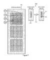
- FIG. 2is block diagram of a structure of a NAND flash system per FBX, in accordance with an embodiment of the invention.
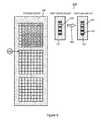
- FIG. 3is a block diagram of a structure of a flash page with control data written to the flash page, in accordance with an embodiment of the invention.
- FIG. 4is a block diagram illustrating an initial state of a storage memory and a cache memory, wherein both memory areas in the storage memory and cache memory contain no data, in accordance with an embodiment of the invention.
- FIG. 5is a block diagram illustrating a subsequent state of the storage memory, wherein the storage memory contains control data, in accordance with an embodiment of the invention.
- FIG. 6is a block diagram illustrating a subsequent state of the storage memory, wherein updates or modification request on control data are performed, in accordance with an embodiment of the invention.
- FIG. 7is a block diagram illustrating a subsequent state of the storage memory and cache memory, wherein the control data is replicated from the storage memory to the cache memory, in accordance with an embodiment of the invention.
- FIG. 8is a block diagram illustrating a subsequent state of the storage memory and cache memory, wherein the control data is partially changed in the cache memory, in accordance with an embodiment of the invention.
- FIG. 9is a block diagram illustrating a subsequent state of the storage memory and cache memory, wherein the dirty cache link list is moved to the for flush link list in the cache memory, in accordance with an embodiment of the invention.
- FIG. 10is a block diagram illustrating a subsequent state of the storage memory and cache memory, wherein the updated control data is now written to the storage memory, in accordance with an embodiment of the invention.
- the terms “include” and “comprise”are used in an open-ended fashion, and thus should be interpreted to mean “include, but not limited to . . . ”.
- the term “couple”is intended to mean either an indirect or direct electrical connection (or an indirect or direct optical connection). Accordingly, if one device is coupled to another device, then that connection may be through a direct electrical (or optical) connection, or through an indirect electrical (or optical) connection via other devices and/or other connections.
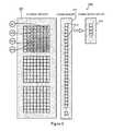
- FIG. 1is a block diagram of an example data storage system 100 (or data storage apparatus 100 ) that can include an embodiment of the invention.
- data storage system 100or data storage apparatus 100
- FIG. 1will realize that an embodiment of the invention can be included in other suitable types of computing systems or data storage systems.
- a software/program 101When the system 100 has initialized and is under normal operation, a software/program 101 (run by the processor requests for the SSD access), for example, will do a read transaction to read data from one or more non-volatile memory devices 102 (e.g., flash devices 102 or flash memory devices 102 ) in the flash storage module 103 or do a write transaction to write data to one or more non-volatile memory devices 102 in the flash storage module 103 .
- the one or more memory devices 102form a memory device array 104 in the flash module 103 .
- the memory device array 104is coupled via a flash interface 105 to a flash memory controller 106 .
- the flash storage module 103is coupled via a flash bus 107 (or memory bus 107 ) to a Direct Memory Access (DMA) controller 108 .
- the DMA controller 108is coupled via a DMA bus interface 114 to a system bus 109 .
- a processor 110 , system memory 111 , and software/program 101are all coupled to the system bus 109 .
- the system 100can include more than one software/program 101 , more than one processor 110 , and/or more than one system memory 111 . Additionally or alternatively, the system 100 can include more than one DMA controller 108 and more than one flash storage module 103 .
- the plurality of flash storage modules 103will form an array (not shown) of flash storage modules 103 .
- System bus 109is a conduit or data path for transferring data between DMA controller 108 , processor 110 , system memory 111 , and software/program 101 .
- Processor 110 , DMA controller 108 , and software/program 101may access system memory 111 via system bus 109 as needed.
- System memory 111may be implemented using any form of memory, such as, for example, various types of DRAM (dynamic random access memory), non-volatile memory, or other types of memory devices.
- a request 115 for a memory transaction(e.g., read or write transaction) from a software/program 101 , typically in the form of an input-output descriptor command, is destined for the processor 110 .
- Descriptor commandsare detailed instructions to be executed by an engine or a module.
- the processor 110interprets that the input-output descriptor command intends to read from memory devices 102 in the flash storage module 103 or intends to write to memory devices 102 in the flash storage module 103 .
- the processor 110is in-charge of issuing all the needed descriptors to one or more Direct Memory Access (DMA) controllers 108 to execute a read memory transaction or write memory transaction in response to the request 115 .
- DMADirect Memory Access
- the DMA controller 108 , flash memory controller 106 , and processor 110allow at least one software/program 101 , to communicate with memory devices 102 within the data storage apparatus 100 .
- the processor 110analyzes and responds to a memory transaction request 115 by generating DMA instructions that will cause the DMA controller 108 to read data from or write data to the flash devices 102 in a flash storage module 103 through the flash memory controller 106 . If this data is available, the flash memory controller 106 retrieves this data, which is transferred to the system memory 111 by the DMA controller 108 , and eventually transferred to the software/program 101 via system bus 109 . Data obtained during this memory read transaction request is hereinafter named “read data”. Similarly, write data from the software/program 101 will cause the DMA controller 108 to write data to the flash devices 102 through the flash memory controller 106 .
- a non-volatile memory device 102 in the flash storage module 103may be, for example, a flash device.
- This flash devicemay be implemented by using a flash memory device that complies with the Open NAND Flash Interface Specification, commonly referred to as ONFI Specification.
- ONFI Specificationis a known device interface standard created by a consortium of technology companies known as the “ONFI Workgroup”.
- the ONFI Workgroupdevelops open standards for NAND Flash memory devices and for devices that communicate with these NAND flash memory devices.
- the ONFI Workgroupis headquartered in Hillsboro, Oreg. Using a flash device that complies with the ONFI Specification is not intended to limit the embodiment(s) disclosed herein.
- Non-Volatile Memory Host Controller InterfaceNVMHCI
- NVMHCINon-Volatile Memory Host Controller Interface
- Members of the NVMHCI working groupinclude Intel Corporation of Santa Clara, Calif., Dell Inc. of Round Rock, Tex., and Microsoft Corporation of Redmond, Wash.
- FIG. 2is block diagram showing a boundary 200 (apparatus 200 or system 200 ) which is also illustrated as a box 200 that represents NAND Flash dies per FBX, in accordance with an embodiment of the invention.
- FBXis a Flash Box which is similar to a Disk Chassis.
- the box 200is the box or boundary of flash memory devices.
- the boundary 200 of flash memoryis set as per FBX.
- Box (or boundary) 200shows a plurality of flash blocks arranged according to flash dies.
- the box 200can be one of the flash memory devices 102 that are shown in the example data storage system 100 of FIG. 1 .
- flash blocks 201 a through 201 jare included in a flash die 201 .
- flash blocks 202 a through 202 jare also included in a flash die 202 .
- each of the flash die 203 , flash die 204 , flash die 205 , flash die 206 , and flash die 207comprises a plurality of flash blocks.
- the flash blocks 203 a through 203 jare in a flash die 203 .
- the flash blocks 204 a through 204 jare in a flash die 204 .
- the flash blocks 205 a through 205 jare in a flash die 205 .
- the flash blocks 206 a through 206 jare in a flash die 206 .
- the flash blocks 207 a through 207 jare in a flash die 207 .
- the flash blocks 210 a through 210 jare in a flash die 210 .
- the flash blocks in a flash diecan vary in number.
- the flash blocks in each of the flash die 201 through 210can vary in number as noted by, for example, the dots symbols 212 .
- the flash dies in the FBX structure 200can vary in number as noted by, for example, the dot symbols 213 .
- Box 214shows which portion within the flash memory 200 from which the control data will be flushed.
- control datawill be flushed from all flash blocks that are included within box 214 such as, for example, (1) flash blocks 201 b , 201 c , 201 d , through 201 e (in flash die 201 ); (2) flash blocks 210 b , 210 c , 210 d , through 210 e (in flash die 210 ); (3) flash blocks 202 b , 202 c , 202 d , through 202 e (in flash die 202 ); (4) flash blocks 203 b through 203 e (in flash die 203 ); (5) flash blocks 204 b through 204 e (in flash die 204 ); (6) flash blocks 205 b through 205 e (in flash die 205 ); (7) flash blocks 206 b through 206 e (in flash die 206 ); (8) flash blocks 207 b , 206 e (in flash die 206
- Each flash blockis subdivided into flash pages.
- the flash block 210 e in box 214is subdivided into flash pages 210 e 1 through 210 e 8 .
- the flash pages in a flash blockmay vary in number.
- the flash block 210 eis subdivided into flash pages 210 e 1 through 210 e 8 , but can have more flash pages or less flash pages.
- a flash blockis subdivided into more flash pages in addition to the flash pages 210 e 1 through 210 e 8 .
- Each flash pageis subdivided into segments.
- the flash page 210 e 1 in flash block 210 eis subdivided into flash segments 210 e 11 through 210 e 18 .
- the flash segments in a flash pagemay vary in number.
- the flash page 210 e 1is subdivided into flash segments 210 e 11 through 210 e 18 , but can have more flash segments or less flash segments.
- a flash pageis subdivided into more flash segments in addition to the segments 210 e 11 through 210 e 18 .
- the notations 250indicate possible example notations representative of the elements (e.g., control blocks area 214 , flash memory 200 per FBX, flash dies 201 through 210 , flash blocks, flash pages, and flash segments) shown in FIG. 2 .
- the notations 250may be varied since the number of elements in FIG. 2 may increase in number and so the notations 250 are not necessarily a limiting format or not necessarily a limiting symbolic convention in an embodiment of the invention.
- FIG. 3is a block diagram of a structure 300 of a flash page with control data written to the flash page, in accordance with an embodiment of the invention.
- Box 301(which is a sample die 301 ) includes arbitrary flash blocks 302 for control data flushing. Flash blocks include flash pages with valid control data flushed on the flash pages.
- these arbitrary flash blockscomprise a flash block 301 a that is a block that contains valid control data and a flash block 301 b is a block that partially contains valid control data.
- Flash block 301 c and flash block 301 dare flash blocks that are erased or do not contain valid control data.
- the number of flash blocks in a sample die 301may vary in number as denoted by the dot symbols 330 .
- a flash blockcontains flash pages.
- flash block 301 aincludes flash pages 301 a 1 through 301 a 8 , wherein valid control data is flushed on or written to each of the flash pages 301 a 1 through 301 a 8 .
- the number of flash pages in the flash block 301 amay vary in number. Therefore, there may be more flash pages (or less flash pages) than the flash pages 301 a 1 through 301 a 8 .
- the next flash block 301 bincludes flash pages 301 b 1 through 301 b 8 , wherein valid control data is flushed on or written to each of the flash pages 301 b 1 through 301 b 4 and wherein the flash pages 301 b 5 through 301 b 8 are erased or do not contain valid control data.
- the number of flash pages in the flash block 301 bmay vary in number. Therefore, there may be more flash pages (or less flash pages) than the flash pages 301 b 1 through 301 b 8 .
- the number of flash pages that is flushed with or written with control datamay vary in number. Therefore, there may be more flash pages (or less flash pages) that is flushed with or written with control data.
- Flash page 301 a 1includes a plurality of flash segments 301 a 11 through 301 a 18 .
- First segment 301 a 11 of flash page 301 a 1contains control data identifier information that identifies the flash page 301 a 1 as containing a control data and information concerning the succeeding flash segments 301 a 12 through 301 a 18 of the flash page 301 a 1 .
- Flash segments 301 a 12 through 301 a 18are flash segments within a flash page that contains control data.
- the number of flash segments in the flash page 301 a 1may vary in number. Therefore, there may be more flash segments (or less flash segments) than the flash segments 301 a 11 through 301 a 18 .
- Block 303shows the information found in the first flash segment 301 a 11 .
- This information 303comprises the signature 305 which identifies the flash page 301 a 1 as a control data page, the sequence number SQN 306 that is used to track control data updates, and the array of identities (e.g., Identity 1 307 , Identity 2 308 , Identity 3 309 , Identity 4 310 , and IdentityN 311 ) wherein N is a suitable integer value and wherein the array describes the control data written from flash segments 301 a 12 up to the last flash segment 301 a 18 of the flash page 301 a 1 . Since the flash segments in a flash page 301 a 1 can vary in number, the identities can vary in number as noted by, for example, the dot symbols 304 .
- the notations 350indicate the notations representative of the elements (e.g., sample die 301 , flash blocks, flash pages, flash segments, sample flash control blocks area 214 , flash memory 200 per FBX, flash dies 201 through 210 , flash blocks, flash pages, and flash segments) shown in FIG. 3 .
- Page information 351is, for example, contained in the first flash segment 301 a 11 and is shown in detail in block 303 .
- Control data 352is in, for example, the flash page 301 a 1 as similarly discussed above in the example of FIG. 3 .
- the data 353is in, for example, the flash pages 301 a 1 through 301 a 8 and flash pages 301 b 1 through 301 b 4 as similarly discussed above in the example of FIG. 3 .
- the page 354which has no data and is an erased area, is similarly discussed above at pages 301 b 5 through 301 b 8 of flash block 301 b and all pages of flash block 301 a and all pages of flash block
- a flash block 302is filled with control data as similarly described above.
- the notations 350may be varied since the number of elements in FIG. 3 may increase in number and so the notations 350 are not necessarily a limiting format or not necessarily a limiting symbolic convention in an embodiment of the invention.
- FIGS. 4 through 10disclose a process of writing a control data with the collection of a modified cache line using a combination technique.
- the process performed in FIGS. 4 through 10may be executed by, for example, the DMA controller 108 through the flash memory controller 106 which accesses the flash memory device 102 .
- a control data flushing system 200 in an embodiment of the inventioncan include the DMA controller 108 , flash memory controller 106 , and as storage device 102 which may be, for example, a flash memory device 102 or a solid state drive (SSD) 102 .
- SSDsolid state drive
- FIG. 4is a block diagram illustrating an initial state of a storage memory 409 and a cache memory 410 , wherein both memory areas in the storage memory 410 and cache memory 410 contain no data, in accordance with an embodiment of the invention.
- the storage memory 409is one or more of the flash memory devices 102 ( FIG. 1 ) and the cache memory 410 can be a memory area in one of the flash devices 102 , a memory area in the flash controller 106 , or a memory area in another part of the flash storage module 103 ( FIG. 1 ).
- the Cache memory 410is divided into a segment size, which is the same size as a flash segment (e.g., flash segment 204 ).
- the initial state of both memory areas 409 and 410contains no data in FIG. 4 , until the system 200 undergoes a constructing process.
- the size of the storage memory 409 and/or size of the cache memory 410can be set to other suitable sizes.
- FIG. 5is a block diagram illustrating a subsequent state of the storage memory 409 , wherein the storage memory 409 contains control data (generally shown as control data 505 ) in a plurality of flash blocks 506 in the storage memory 409 , in accordance with an embodiment of the invention.
- the control data(or metadata) can be scattered in the storage memory 409 and would be in a volatile stored form in the cache memory 410 .
- FIG. 6is a block diagram illustrating a subsequent state of the storage memory 409 , wherein updates or modification request on control data are performed, in accordance with an embodiment of the invention. Updates or modifications requests are performed on the control data 611 , 612 , 613 , and 614 in the storage memory 409 .
- the system 200will ask for a vacant cache memory area 615 in the cache memory 410 , and the next block is identified as a Clean Cache Link List 616 in the cache memory 410 .
- FIG. 7is a block diagram illustrating a subsequent state of the storage memory 409 and cache memory 410 , wherein the control data is replicated from the storage memory to the cache memory, in accordance with an embodiment of the invention.
- Control data 717 , 718 , 719 , and 720(also shown as control data 611 , 612 , 613 , and 614 in FIG. 6 , respectively) is replicated from storage memory 409 to cache memory 410 .
- control data 717 , 718 , 719 , and 720are symbolically represented as, “g”, “l”, “aj”, and “ap”.
- the Cache memory 410holds the target data (control data that is modified) in this operation.
- the previous clean cache link list 616is moved ( 722 ) to the dirty cache link list 721 so that the dirty cache link list 721 is partially changed by moving ( 722 ) the previous clean cache link list 616 to the dirty cache link list 721 . Therefore, the dirty cache link list 721 in the cache memory 410 will first contain the example control data sets 723 that are symbolically represented as “aj”, “g”, “l”, and “ap”, and when the control data 717 - 720 are updated or modified, the previous clean link list 616 is moved ( 722 ) to the dirty cache link list 721 so that the dirty cache link list 721 is changed into the updated control data 823 of FIG. 8 . Therefore, the cache memory 410 is used to update or modify the control data.
- FIG. 8is a block diagram illustrating a subsequent state of the storage memory 409 and cache memory 410 , wherein the control data 823 is partially changed in the cache memory 409 , in accordance with an embodiment of the invention.
- the control data 823in the dirty cache link list 721
- FIG. 9is a block diagram illustrating a subsequent state of the storage memory 409 and cache memory 410 , wherein the dirty cache link list 721 is moved ( 926 ) to the for flush link list 925 in the cache memory 410 , in accordance with an embodiment of the invention. Therefore, the cache line 922 in the for flush link list 925 (in cache memory 410 ) will contain the updated control data 950 . Once the cache line 922 (which has the updated control data 950 is ready to be written into the storage memory 409 , the dirty cache link list 721 will be moved ( 926 ) to the flush link list 725 . The control data flushing system 200 will ask for a free page 924 in storage memory 409 in order to write the updated control data 950 in cache memory 410 from the for flush link list 925 .
- FIG. 10is a block diagram illustrating a subsequent state of the storage memory 409 and cache memory 410 , wherein the updated control data 950 is now written to the storage memory 409 , in accordance with an embodiment of the invention.
- Control data 1027 , 1028 , 1029 , and 1030are the old control data that was previously modified, and the updated control data 950 are written to the new flash page 1031 in the storage memory 409 .
- the used cache line 922retains its control data 932 (which is also the updated control data 950 of FIG. 9 ) and the system 200 returns ( 933 ) to the for flush link list 925 to the clean cache memory link list 721 .
- An embodiment of the inventionadvantageously avoids the need to save the next level pointer because in this method embodiment (or algorithm) of the invention, an indicator/header representing each page is provided.
- the algorithmsearches every page in the system so that the method determines what is represented in each header. The system performance in run-time will be faster because the algorithm does not need to update the high level pointer.
- the directory DIR1which is a pointer to the directory zero section
- the DIR1 sectionwill need to be saved because of the update to DIR1.
- an algorithm in an embodiment of the inventionat I/O (input/output) time, after the directory zero section is saved, there is no need to update the DIR1 entry.
- the algorithmreads a small segment of each flash page where the control header is stored and thus the algorithm identifies the content of each flash page.
- the algorithmreads the control header (block 306 ) and during boot-up, the algorithm compares the sequence numbers and the higher sequence number is updated control data version and thus the newest directory section will have a higher SQN number.
- An algorithm in one embodiment of the inventionadvantageously avoids the logging (journaling) of a saved directory section.
Landscapes
- Engineering & Computer Science (AREA)
- Theoretical Computer Science (AREA)
- Physics & Mathematics (AREA)
- General Engineering & Computer Science (AREA)
- General Physics & Mathematics (AREA)
- Human Computer Interaction (AREA)
- Computer Security & Cryptography (AREA)
- Information Retrieval, Db Structures And Fs Structures Therefor (AREA)
Abstract
Description
This application is a continuation in part of U.S. application Ser. No. 14/690,370 which claims the benefit of and priority to U.S. Provisional Application 61/981,165, filed 17 Apr. 2014. This U.S. Provisional Application 61/981,165 and U.S. application Ser. No. 14/690,370 are hereby fully incorporated herein by reference.
Embodiments of the invention relate generally to data storage systems. Embodiments of the invention also relate to writing scattered cache memory data to a flash device. Embodiments of the invention also relate to writing volatile scattered memory metadata to a flash device.
The background description provided herein is for the purpose of generally presenting the context of the disclosure of the invention. Work of the presently named inventors, to the extent the work is described in this background section, as well as aspects of the description that may not otherwise qualify as prior art at the time of filing, are neither expressly nor impliedly admitted as prior art against this present disclosure of the invention.
In a typical data storage system, a minimum size of cache memory is used to read or write a data. Where that size is large enough for a small change, this conventional approach does not maximize the write amplification. This type of write process in a permanent storage limits some certain types of control data. As known to those skilled in the art, write amplification is an undesirable phenomenon associated with flash memory and solid-state drives (SSDs) where the actual amount of physical information written is a multiple of the logical amount intended to be written.
Additionally, in a typical data storage system, the size used for the cache allocation is the same as the flash page size. By this approach, the data will transfer with difficulty.
Therefore, there is a continuing need to overcome the constraints or disadvantages of current conventional systems.
Embodiments of the invention relate generally to data storage systems. Embodiments of the invention also relate to writing scattered cache memory data to a flash device. Embodiments of the invention also relate to writing volatile scattered memory metadata to a flash device.
In an embodiment of the invention, a method and apparatus will update the data by using a temporary storage and will transfer the modified data to a new location in a permanent storage. This design or feature is used for write purposes of control data from cache memory to storage memory. By using the cache memory as a temporary location for modifying data, the design maximizes the write amplification.
In an embodiment of the invention, a method comprises: requesting an update on a control data in at least one flash block in a storage memory; replicating, from the storage memory to a cache memory, the control data to be updated; moving a clean cache link list to a dirty cache link list so that the dirty cache link list is changed to reflect the update on the control data; and moving the dirty cache link list to a for-flush link list and writing an updated control data from the for-flush link list to a free flash page in the storage memory.
In another embodiment of the invention, an apparatus comprises: a control data flushing system configured to: request an update on a control data in at least one flash block in a storage memory; replicate, from the storage memory to a cache memory, the control data to be updated; move a clean cache link list to a dirty cache link list so that the dirty cache link list is changed to reflect the update on the control data; and move the dirty cache link list to a for-flush link list and write an updated control data from the for-flush link list to a free flash page in the storage memory.
In yet another embodiment of the invention, an article of manufacture, comprises a non-transient computer-readable medium having stored thereon instructions operable to permit an apparatus to: request an update on a control data in at least one flash block in a storage memory; replicate, from the storage memory to a cache memory, the control data to be updated; move a clean cache link list to a dirty cache link list so that the dirty cache link list is changed to reflect the update on the control data; and move the dirty cache link list to a for-flush link list and write an updated control data from the for-flush link list to a free flash page in the storage memory.
In another embodiment of the invention, a method comprises: requesting an update or modification on a control data in at least one flash block in a storage memory; requesting a cache memory; replicating, from the storage memory to the cache memory, the control data to be updated or to be modified; moving a clean cache link list to a dirty cache link list so that the dirty cache link list is changed to reflect the update or modification on the control data; and moving the dirty cache link list to a for-flush link list and writing an updated control data from the for-flush link list to a free flash page in the storage memory.
In another embodiment of the invention, an article of manufacture comprises: a non-transient computer-readable medium having stored thereon instructions operable to permit an apparatus to: request an update or modification on a control data in at least one flash block in a storage memory; request a cache memory; replicate, from the storage memory to the cache memory, the control data to be updated or to be modified; move a clean cache link list to a dirty cache link list so that the dirty cache link list is changed to reflect the update or modification on the control data; and move the dirty cache link list to a for-flush link list and write an updated control data from the for-flush link list to a free flash page in the storage memory.
In another embodiment of the invention, apparatus comprises: a control data flushing system configured to: request an update or modification on a control data in at least one flash block in a storage memory; request a cache memory; replicate, from the storage memory to the cache memory, the control data to be updated or to be modified; move a clean cache link list to a dirty cache link list so that the dirty cache link list is changed to reflect the update or modification on the control data; and move the dirty cache link list to a for-flush link list and write an updated control data from the for-flush link list to a free flash page in the storage memory.
It is to be understood that both the foregoing general description and the following detailed description are exemplary and explanatory only and are not restrictive of the invention, as claimed.
The accompanying drawings, which are incorporated in and constitute a part of this specification, illustrate one (several) embodiment(s) of the invention and together with the description, serve to explain the principles of the invention.
Non-limiting and non-exhaustive embodiments of the present invention are described with reference to the following figures, wherein like reference numerals refer to like parts throughout the various views unless otherwise specified.
It is to be noted, however, that the appended drawings illustrate only typical embodiments of this invention and are therefore not to be considered limiting of its scope, for the present invention may admit to other equally effective embodiments.
In the following detailed description, for purposes of explanation, numerous specific details are set forth to provide a thorough understanding of the various embodiments of the present invention. Those of ordinary skill in the art will realize that these various embodiments of the present invention are illustrative only and are not intended to be limiting in any way. Other embodiments of the present invention will readily suggest themselves to such skilled persons having the benefit of this disclosure.
In addition, for clarity purposes, not all of the routine features of the embodiments described herein are shown or described. One of ordinary skill in the art would readily appreciate that in the development of any such actual implementation, numerous implementation-specific decisions may be required to achieve specific design objectives. These design objectives will vary from one implementation to another and from one developer to another. Moreover, it will be appreciated that such a development effort might be complex and time-consuming, but would nevertheless be a routine engineering undertaking for those of ordinary skill in the art having the benefit of this disclosure. The various embodiments disclosed herein are not intended to limit the scope and spirit of the herein disclosure.
Exemplary embodiments for carrying out the principles of the present invention are described herein with reference to the drawings. However, the present invention is not limited to the specifically described and illustrated embodiments. A person skilled in the art will appreciate that many other embodiments are possible without deviating from the basic concept of the invention. Therefore, the principles of the present invention extend to any work that falls within the scope of the appended claims.
As used herein, the terms “a” and “an” herein do not denote a limitation of quantity, but rather denote the presence of at least one of the referenced items.
In the following description and in the claims, the terms “include” and “comprise” are used in an open-ended fashion, and thus should be interpreted to mean “include, but not limited to . . . ”. Also, the term “couple” (or “coupled”) is intended to mean either an indirect or direct electrical connection (or an indirect or direct optical connection). Accordingly, if one device is coupled to another device, then that connection may be through a direct electrical (or optical) connection, or through an indirect electrical (or optical) connection via other devices and/or other connections.
When thesystem 100 has initialized and is under normal operation, a software/program101 (run by the processor requests for the SSD access), for example, will do a read transaction to read data from one or more non-volatile memory devices102 (e.g.,flash devices 102 or flash memory devices102) in theflash storage module 103 or do a write transaction to write data to one or morenon-volatile memory devices 102 in theflash storage module 103. Typically, the one ormore memory devices 102 form amemory device array 104 in theflash module 103. Thememory device array 104 is coupled via aflash interface 105 to aflash memory controller 106.
Theflash storage module 103 is coupled via a flash bus107 (or memory bus107) to a Direct Memory Access (DMA)controller 108. TheDMA controller 108 is coupled via aDMA bus interface 114 to asystem bus 109.
Aprocessor 110,system memory 111, and software/program 101 are all coupled to thesystem bus 109. Thesystem 100 can include more than one software/program 101, more than oneprocessor 110, and/or more than onesystem memory 111. Additionally or alternatively, thesystem 100 can include more than oneDMA controller 108 and more than oneflash storage module 103. In an embodiment of the invention that includes a plurality offlash storage modules 103 and a plurality ofDMA controllers 108, wherein eachflash storage module 103 is coupled via arespective flash bus 107 to arespective DMA controller 108, the plurality offlash storage modules 103 will form an array (not shown) offlash storage modules 103.
A request115 for a memory transaction (e.g., read or write transaction) from a software/program 101, typically in the form of an input-output descriptor command, is destined for theprocessor 110. Descriptor commands are detailed instructions to be executed by an engine or a module. Theprocessor 110 interprets that the input-output descriptor command intends to read frommemory devices 102 in theflash storage module 103 or intends to write tomemory devices 102 in theflash storage module 103. Theprocessor 110 is in-charge of issuing all the needed descriptors to one or more Direct Memory Access (DMA)controllers 108 to execute a read memory transaction or write memory transaction in response to the request115. Therefore, theDMA controller 108,flash memory controller 106, andprocessor 110 allow at least one software/program 101, to communicate withmemory devices 102 within thedata storage apparatus 100. Operating under a program control (such as a control by software or firmware), theprocessor 110 analyzes and responds to a memory transaction request115 by generating DMA instructions that will cause theDMA controller 108 to read data from or write data to theflash devices 102 in aflash storage module 103 through theflash memory controller 106. If this data is available, theflash memory controller 106 retrieves this data, which is transferred to thesystem memory 111 by theDMA controller 108, and eventually transferred to the software/program 101 viasystem bus 109. Data obtained during this memory read transaction request is hereinafter named “read data”. Similarly, write data from the software/program 101 will cause theDMA controller 108 to write data to theflash devices 102 through theflash memory controller 106.
Anon-volatile memory device 102 in theflash storage module 103 may be, for example, a flash device. This flash device may be implemented by using a flash memory device that complies with the Open NAND Flash Interface Specification, commonly referred to as ONFI Specification. The term “ONFI Specification” is a known device interface standard created by a consortium of technology companies known as the “ONFI Workgroup”. The ONFI Workgroup develops open standards for NAND Flash memory devices and for devices that communicate with these NAND flash memory devices. The ONFI Workgroup is headquartered in Hillsboro, Oreg. Using a flash device that complies with the ONFI Specification is not intended to limit the embodiment(s) disclosed herein. One of ordinary skill in the art having the benefit of this disclosure would readily recognize that other types of flash devices employing different device interface protocols may be used, such as protocols that are compatible with the standards created through the Non-Volatile Memory Host Controller Interface (NVMHCI) working group. Members of the NVMHCI working group include Intel Corporation of Santa Clara, Calif., Dell Inc. of Round Rock, Tex., and Microsoft Corporation of Redmond, Wash.
Those skilled in the art with the benefit of this disclosure will realize that there can be multiple components in thesystem 100 such as, for example, multiple processors, multiple memory arrays, multiple DMA controllers, and/or multiple flash controllers.
Box (or boundary)200 shows a plurality of flash blocks arranged according to flash dies. Thebox 200 can be one of theflash memory devices 102 that are shown in the exampledata storage system 100 ofFIG. 1 . For example, flash blocks201athrough201jare included in aflash die 201. Similarly, flash blocks202athrough202jare also included in aflash die 202. Similarly, each of the flash die203, flash die204, flash die205, flash die206, and flash die207 comprises a plurality of flash blocks. For example, the flash blocks203athrough203jare in aflash die 203. The flash blocks204athrough204jare in aflash die 204. The flash blocks205athrough205jare in aflash die 205. The flash blocks206athrough206jare in aflash die 206. The flash blocks207athrough207jare in aflash die 207. The flash blocks210athrough210jare in aflash die 210. The flash blocks in a flash die can vary in number. For example, the flash blocks in each of the flash die201 through210 can vary in number as noted by, for example, thedots symbols 212. The flash dies in theFBX structure 200 can vary in number as noted by, for example, thedot symbols 213. For example, there can be more flash dies in theFBX structure 200 in addition to the flash dies201,202, through210. Alternatively, there can be less flash dies in theFBX structure 200 than the flash dies201,202, through210.
Box214 (or boundary214) shows which portion within theflash memory 200 from which the control data will be flushed. In the example ofFIG. 1 , control data will be flushed from all flash blocks that are included withinbox 214 such as, for example, (1) flash blocks201b,201c,201d, through201e(in flash die201); (2) flash blocks210b,210c,210d, through210e(in flash die210); (3) flash blocks202b,202c,202d, through202e(in flash die202); (4) flash blocks203bthrough203e(in flash die203); (5) flash blocks204bthrough204e(in flash die204); (6) flash blocks205bthrough205e(in flash die205); (7) flash blocks206bthrough206e(in flash die206); (8) flash blocks207bthrough207e(in flash die207); and (9) flash blocks210bthrough210e(in flash die210). The flash blocks that will have control data to be flushed in thebox 214 may vary in number as noted by, for example, the dot symbols211 (in boundary214) and dot symbols213 (in boundary200).
Each flash block is subdivided into flash pages. For example, theflash block 210einbox 214 is subdivided intoflash pages 210e1 through210e8. The flash pages in a flash block may vary in number. For example, theflash block 210eis subdivided intoflash pages 210e1 through210e8, but can have more flash pages or less flash pages. In typical implementations, a flash block is subdivided into more flash pages in addition to theflash pages 210e1 through210e8.
Each flash page is subdivided into segments. For example, theflash page 210e1 inflash block 210eis subdivided intoflash segments 210e11 through210e18. The flash segments in a flash page may vary in number. For example, theflash page 210e1 is subdivided intoflash segments 210e11 through210e18, but can have more flash segments or less flash segments. In typical implementations, a flash page is subdivided into more flash segments in addition to thesegments 210e11 through210e18.
Thenotations 250 indicate possible example notations representative of the elements (e.g.,control blocks area 214,flash memory 200 per FBX, flash dies201 through210, flash blocks, flash pages, and flash segments) shown inFIG. 2 . However, thenotations 250 may be varied since the number of elements inFIG. 2 may increase in number and so thenotations 250 are not necessarily a limiting format or not necessarily a limiting symbolic convention in an embodiment of the invention.
A flash block contains flash pages. For example, flash block301aincludesflash pages 301a1 through301a8, wherein valid control data is flushed on or written to each of theflash pages 301a1 through301a8. The number of flash pages in theflash block 301amay vary in number. Therefore, there may be more flash pages (or less flash pages) than theflash pages 301a1 through301a8.
Thenext flash block 301bincludesflash pages 301b1 through301b8, wherein valid control data is flushed on or written to each of theflash pages 301b1 through301b4 and wherein theflash pages 301b5 through301b8 are erased or do not contain valid control data. The number of flash pages in theflash block 301bmay vary in number. Therefore, there may be more flash pages (or less flash pages) than theflash pages 301b1 through301b8. The number of flash pages that is flushed with or written with control data may vary in number. Therefore, there may be more flash pages (or less flash pages) that is flushed with or written with control data.
Thenotations 350 indicate the notations representative of the elements (e.g., sample die301, flash blocks, flash pages, flash segments, sample flashcontrol blocks area 214,flash memory 200 per FBX, flash dies201 through210, flash blocks, flash pages, and flash segments) shown inFIG. 3 .Page information 351 is, for example, contained in thefirst flash segment 301a11 and is shown in detail inblock 303.Control data 352 is in, for example, theflash page 301a1 as similarly discussed above in the example ofFIG. 3 . Thedata 353 is in, for example, theflash pages 301a1 through301a8 andflash pages 301b1 through301b4 as similarly discussed above in the example ofFIG. 3 . Thepage 354, which has no data and is an erased area, is similarly discussed above atpages 301b5 through301b8 offlash block 301band all pages offlash block 301aand all pages offlash block 301d.
Aflash block 302 is filled with control data as similarly described above. However, thenotations 350 may be varied since the number of elements inFIG. 3 may increase in number and so thenotations 350 are not necessarily a limiting format or not necessarily a limiting symbolic convention in an embodiment of the invention.
Reference is now made toFIGS. 4 through 10 which disclose a process of writing a control data with the collection of a modified cache line using a combination technique. The process performed inFIGS. 4 through 10 may be executed by, for example, theDMA controller 108 through theflash memory controller 106 which accesses theflash memory device 102. Therefore, a controldata flushing system 200 in an embodiment of the invention can include theDMA controller 108,flash memory controller 106, and asstorage device 102 which may be, for example, aflash memory device 102 or a solid state drive (SSD)102.
TheCache memory 410 is divided into a segment size, which is the same size as a flash segment (e.g., flash segment204). The initial state of bothmemory areas FIG. 4 , until thesystem 200 undergoes a constructing process. The size of thestorage memory 409 and/or size of thecache memory 410 can be set to other suitable sizes.
An embodiment of the invention advantageously avoids the need to save the next level pointer because in this method embodiment (or algorithm) of the invention, an indicator/header representing each page is provided. During power-on and/or boot-up, the algorithm searches every page in the system so that the method determines what is represented in each header. The system performance in run-time will be faster because the algorithm does not need to update the high level pointer. In contrast with regard to a previous approach, during run-time, there is a domino effect wherein if a directory zero section is saved, the directory DIR1 (which is a pointer to the directory zero section) will also need to be updated and the DIR1 section will need to be saved because of the update to DIR1. In an algorithm in an embodiment of the invention, at I/O (input/output) time, after the directory zero section is saved, there is no need to update the DIR1 entry. The algorithm reads a small segment of each flash page where the control header is stored and thus the algorithm identifies the content of each flash page. During boot-up, the algorithm reads the control header (block306) and during boot-up, the algorithm compares the sequence numbers and the higher sequence number is updated control data version and thus the newest directory section will have a higher SQN number. An algorithm in one embodiment of the invention advantageously avoids the logging (journaling) of a saved directory section.
Foregoing described embodiments of the invention are provided as illustrations and descriptions. They are not intended to limit the invention to precise form described. In particular, it is contemplated that functional implementation of invention described herein may be implemented equivalently in hardware, software, firmware, and/or other available functional components or building blocks, and that networks may be wired, wireless, or a combination of wired and wireless.
It is also within the scope of the present invention to implement a program or code that can be stored in a non-transient machine-readable (or non-transient computer-readable medium) having stored thereon instructions that permit a method (or that permit a computer) to perform any of the inventive techniques described above, or a program or code that can be stored in an article of manufacture that includes a non-transient computer readable medium on which computer-readable instructions for carrying out embodiments of the inventive techniques are stored. Other variations and modifications of the above-described embodiments and methods are possible in light of the teaching discussed herein.
The above description of illustrated embodiments of the invention, including what is described in the Abstract, is not intended to be exhaustive or to limit the invention to the precise forms disclosed. While specific embodiments of, and examples for, the invention are described herein for illustrative purposes, various equivalent modifications are possible within the scope of the invention, as those skilled in the relevant art will recognize.
These modifications can be made to the invention in light of the above detailed description. The terms used in the following claims should not be construed to limit the invention to the specific embodiments disclosed in the specification and the claims. Rather, the scope of the invention is to be determined entirely by the following claims, which are to be construed in accordance with established doctrines of claim interpretation.
Claims (20)
1. A method, comprising:
requesting an update on a control data in at least one flash block in a storage memory;
replicating, from the storage memory to a cache memory, the control data to be updated;
moving a clean cache link list in the cache memory to a dirty cache link list in the cache memory so that the dirty cache link list is changed to reflect the update on the control data, wherein the dirty cache link list will first contain the control data without the update prior to moving the clean cache link list to the dirty cache link list, and wherein the dirty cache link list is changed into an updated control data after the control data is updated and the clean cache link list is moved to the dirty cache link list;
moving the dirty cache link list to a for-flush link list in the cache memory so that the for-flush link list will contain the updated control data; and
asking for a free flash page in the storage memory;
and writing the updated control data from the for-flush link list to the free flash page in the storage memory.
2. The method ofclaim 1 , wherein the cache memory is used as a temporary location for modifying the control data.
3. The method ofclaim 1 , wherein the at least one flash block comprises at least one flash page and wherein the at least one flash page comprises a control data identifier information and a control data information.
4. The method ofclaim 1 , further comprising:
returning the for-flush link list to the clean cache link list in the cache memory.
5. The method ofclaim 1 , wherein the dirty cache link list is moved to the for-flush link list prior to writing the updated control data to the storage memory.
6. The method ofclaim 1 , wherein the storage memory comprises at least one solid state drive (SSD).
7. The method ofclaim 1 , wherein the storage memory comprises at least one flash memory device.
8. An apparatus, comprising:
a control data flushing system configured to:
request an update on a control data in at least one flash block in a storage memory;
replicate, from the storage memory to a cache memory, the control data to be updated;
move a clean cache link list in the cache memory to a dirty cache link list in the cache memory so that the dirty cache link list is changed to reflect the update on the control data, wherein the dirty cache link list will first contain the control data without the update prior to moving the clean cache link list to the dirty cache link list, and wherein the dirty cache link list is changed into an updated control data after the control data is updated and the clean cache link list is moved to the dirty cache link list;
move the dirty cache link list to a for-flush link list in the cache memory so that the for-flush link list will contain the updated control data;
ask for a free flash page in the storage memory; and
write the updated control data from the for-flush link list to the free flash page in the storage memory.
9. The apparatus ofclaim 8 , wherein the cache memory is used as a temporary location for modifying the control data.
10. The apparatus ofclaim 8 , wherein the at least one flash block comprises at least one flash page and wherein the at least one flash page comprises a control data identifier information and a control data information.
11. The apparatus ofclaim 8 , wherein the control data flushing system is configured to return the for-flush link list to the clean cache link list in the cache memory.
12. The apparatus ofclaim 8 , wherein the dirty cache link list is moved to the for-flush link list prior to writing the updated control data to the storage memory.
13. The apparatus ofclaim 8 , wherein the storage memory comprises at least one solid state drive (SSD).
14. The apparatus ofclaim 8 , wherein the storage memory comprises at least one flash memory device.
15. An article of manufacture, comprising:
a non-transitory computer-readable medium having stored thereon instructions operable to permit an apparatus to perform a method comprising:
requesting an update on a control data in at least one flash block in a storage memory;
replicating, from the storage memory to a cache memory, the control data to be updated;
moving a clean cache link list in the cache memory to a dirty cache link list in the cache memory so that the dirty cache link list is changed to reflect the update on the control data, wherein the dirty cache link list will first contain the control data without the update prior to moving the clean cache link list to the dirty cache link list, and wherein the dirty cache link list is changed into an updated control data after the control data is updated and the clean cache link list is moved to the dirty cache link list;
moving the dirty cache link list to a for-flush link list in the cache memory so that the for-flush link list will contain the updated control data;
asking for a free flash page in the storage memory; and
writing the updated control data from the for-flush link list to the free flash page in the storage memory.
16. The article of manufacture ofclaim 15 , wherein the instructions are operable to permit the apparatus to perform a method further comprising: returning the for-flush link list to the clean cache link list in the cache memory.
17. The article of manufacture ofclaim 15 , wherein the dirty cache link list is moved to the for-flush link list prior to writing the updated control data to the storage memory.
18. The article of manufacture ofclaim 15 , wherein the storage memory comprises at least one solid state drive (SSD).
19. The article of manufacture ofclaim 15 , wherein the storage memory comprises at least one flash memory device.
20. The article of manufacture ofclaim 15 , wherein the cache memory is used as a temporary location for modifying the control data.
Priority Applications (1)
| Application Number | Priority Date | Filing Date | Title |
|---|---|---|---|
| US15/170,768US10055150B1 (en) | 2014-04-17 | 2016-06-01 | Writing volatile scattered memory metadata to flash device |
Applications Claiming Priority (6)
| Application Number | Priority Date | Filing Date | Title |
|---|---|---|---|
| US201461980594P | 2014-04-17 | 2014-04-17 | |
| US201461981150P | 2014-04-17 | 2014-04-17 | |
| US201461980634P | 2014-04-17 | 2014-04-17 | |
| US201461981165P | 2014-04-17 | 2014-04-17 | |
| US14/690,370US9811461B1 (en) | 2014-04-17 | 2015-04-17 | Data storage system |
| US15/170,768US10055150B1 (en) | 2014-04-17 | 2016-06-01 | Writing volatile scattered memory metadata to flash device |
Related Parent Applications (1)
| Application Number | Title | Priority Date | Filing Date |
|---|---|---|---|
| US14/690,370Continuation-In-PartUS9811461B1 (en) | 2014-04-17 | 2015-04-17 | Data storage system |
Publications (1)
| Publication Number | Publication Date |
|---|---|
| US10055150B1true US10055150B1 (en) | 2018-08-21 |
Family
ID=63143892
Family Applications (1)
| Application Number | Title | Priority Date | Filing Date |
|---|---|---|---|
| US15/170,768ActiveUS10055150B1 (en) | 2014-04-17 | 2016-06-01 | Writing volatile scattered memory metadata to flash device |
Country Status (1)
| Country | Link |
|---|---|
| US (1) | US10055150B1 (en) |
Cited By (9)
| Publication number | Priority date | Publication date | Assignee | Title |
|---|---|---|---|---|
| US10261704B1 (en)* | 2016-06-29 | 2019-04-16 | EMC IP Holding Company LLC | Linked lists in flash memory |
| US10353820B2 (en) | 2016-06-29 | 2019-07-16 | EMC IP Holding Company LLC | Low-overhead index for a flash cache |
| US10353607B2 (en) | 2016-06-29 | 2019-07-16 | EMC IP Holding Company LLC | Bloom filters in a flash memory |
| US10459807B2 (en)* | 2017-05-23 | 2019-10-29 | International Business Machines Corporation | Determining modified portions of a RAID storage array |
| US10521123B2 (en) | 2016-06-29 | 2019-12-31 | EMC IP Holding Company LLC | Additive library for data structures in a flash memory |
| US11106373B2 (en) | 2016-06-29 | 2021-08-31 | EMC IP Holding Company LLC | Flash interface for processing dataset |
| US11106586B2 (en) | 2016-06-29 | 2021-08-31 | EMC IP Holding Company LLC | Systems and methods for rebuilding a cache index |
| US20210365576A1 (en)* | 2020-05-19 | 2021-11-25 | T-Mobile Usa, Inc. | Multistage database security |
| US20220269608A1 (en)* | 2021-02-20 | 2022-08-25 | Realtek Semiconductor Corporation | Linked list searching method and linked list searching device |
Citations (341)
| Publication number | Priority date | Publication date | Assignee | Title |
|---|---|---|---|---|
| US4402040A (en) | 1980-09-24 | 1983-08-30 | Raytheon Company | Distributed bus arbitration method and apparatus |
| US4403283A (en) | 1980-07-28 | 1983-09-06 | Ncr Corporation | Extended memory system and method |
| US4752871A (en) | 1985-09-30 | 1988-06-21 | Motorola, Inc. | Single-chip microcomputer having a program register for controlling two EEPROM arrays |
| US4967344A (en) | 1985-03-26 | 1990-10-30 | Codex Corporation | Interconnection network for multiple processors |
| US5111058A (en) | 1990-05-23 | 1992-05-05 | Martin Richard A | Circuit for sustaining power supply output following momentary interruption of commercial a.c. power |
| USRE34100E (en) | 1987-01-12 | 1992-10-13 | Seagate Technology, Inc. | Data error correction system |
| US5222046A (en) | 1988-02-17 | 1993-06-22 | Intel Corporation | Processor controlled command port architecture for flash memory |
| WO1994006210A1 (en) | 1992-08-28 | 1994-03-17 | Prabhakar Goel | Multichip ic design using tdm |
| US5297148A (en) | 1989-04-13 | 1994-03-22 | Sundisk Corporation | Flash eeprom system |
| US5339404A (en) | 1991-05-28 | 1994-08-16 | International Business Machines Corporation | Asynchronous TMR processing system |
| US5341339A (en) | 1992-10-30 | 1994-08-23 | Intel Corporation | Method for wear leveling in a flash EEPROM memory |
| US5371709A (en) | 1993-04-01 | 1994-12-06 | Microchip Technology Incorporated | Power management system for serial EEPROM device |
| US5379401A (en) | 1992-03-31 | 1995-01-03 | Intel Corporation | Flash memory card including circuitry for selectively providing masked and unmasked ready/busy output signals |
| US5388083A (en) | 1993-03-26 | 1995-02-07 | Cirrus Logic, Inc. | Flash memory mass storage architecture |
| US5396468A (en) | 1991-03-15 | 1995-03-07 | Sundisk Corporation | Streamlined write operation for EEPROM system |
| US5406529A (en) | 1992-09-22 | 1995-04-11 | International Business Machines Corporation | Flash non-volatile memory |
| US5432748A (en) | 1992-11-13 | 1995-07-11 | Silicon Storager Technology, Inc. | Solid state peripheral storage device |
| US5448577A (en) | 1992-10-30 | 1995-09-05 | Intel Corporation | Method for reliably storing non-data fields in a flash EEPROM memory array |
| US5459850A (en) | 1993-02-19 | 1995-10-17 | Conner Peripherals, Inc. | Flash solid state drive that emulates a disk drive and stores variable length and fixed lenth data blocks |
| US5479638A (en) | 1993-03-26 | 1995-12-26 | Cirrus Logic, Inc. | Flash memory mass storage architecture incorporation wear leveling technique |
| US5485595A (en) | 1993-03-26 | 1996-01-16 | Cirrus Logic, Inc. | Flash memory mass storage architecture incorporating wear leveling technique without using cam cells |
| US5488711A (en) | 1993-04-01 | 1996-01-30 | Microchip Technology Incorporated | Serial EEPROM device and associated method for reducing data load time using a page mode write cache |
| US5509134A (en) | 1993-06-30 | 1996-04-16 | Intel Corporation | Method and apparatus for execution of operations in a flash memory array |
| US5513138A (en) | 1993-05-13 | 1996-04-30 | Ricoh Co., Ltd. | Memory card having a plurality of EEPROM chips |
| US5524231A (en) | 1993-06-30 | 1996-06-04 | Intel Corporation | Nonvolatile memory card with an address table and an address translation logic for mapping out defective blocks within the memory card |
| US5530828A (en) | 1992-06-22 | 1996-06-25 | Hitachi, Ltd. | Semiconductor storage device including a controller for continuously writing data to and erasing data from a plurality of flash memories |
| US5535356A (en) | 1991-09-09 | 1996-07-09 | Samsung Electronics Co., Ltd. | Digital data recording/playback system utilizing EEPROM and ROM memories as a storage medium |
| US5535328A (en) | 1989-04-13 | 1996-07-09 | Sandisk Corporation | Non-volatile memory system card with flash erasable sectors of EEprom cells including a mechanism for substituting defective cells |
| US5542042A (en) | 1993-05-27 | 1996-07-30 | Whirlpool Corporation | Method and apparatus for monitoring volatile memory validity |
| US5542082A (en) | 1990-12-06 | 1996-07-30 | Tandberg Data A/S | Data storage system connected to a host computer system and having removable data storage media and equipped to read a control program from the removable media into storage employing ID comparison scheme |
| US5548741A (en) | 1991-02-07 | 1996-08-20 | Fuji Photo Film Co., Ltd. | IC memory card system having a host processor selectively operable with an IC memory card including either an SRAM or an EEPROM |
| US5559956A (en) | 1992-01-10 | 1996-09-24 | Kabushiki Kaisha Toshiba | Storage system with a flash memory module |
| US5568423A (en) | 1995-04-14 | 1996-10-22 | Unisys Corporation | Flash memory wear leveling system providing immediate direct access to microprocessor |
| US5568439A (en) | 1988-06-08 | 1996-10-22 | Harari; Eliyahou | Flash EEPROM system which maintains individual memory block cycle counts |
| US5572466A (en) | 1992-10-06 | 1996-11-05 | Kabushiki Kaisha Toshiba | Flash memory chips |
| US5594883A (en) | 1993-04-14 | 1997-01-14 | International Business Machines Corporation | Hierarchical data storage system employing contemporaneous transfer of designated data pages to long write and short read cycle memory |
| US5603001A (en) | 1994-05-09 | 1997-02-11 | Kabushiki Kaisha Toshiba | Semiconductor disk system having a plurality of flash memories |
| US5606529A (en) | 1994-12-20 | 1997-02-25 | Hitachi, Ltd. | Semiconductor disk storage |
| US5606532A (en) | 1995-03-17 | 1997-02-25 | Atmel Corporation | EEPROM array with flash-like core |
| US5619470A (en) | 1994-08-17 | 1997-04-08 | Sharp Kabushiki Kaisha | Non-volatile dynamic random access memory |
| US5627783A (en) | 1995-01-31 | 1997-05-06 | Mitsubishi Denki Kabushiki Kaisha | Semiconductor disk device |
| US5640349A (en) | 1994-08-31 | 1997-06-17 | Tdk Corporation | Flash memory system |
| US5644784A (en) | 1995-03-03 | 1997-07-01 | Intel Corporation | Linear list based DMA control structure |
| US5682509A (en) | 1995-12-13 | 1997-10-28 | Ast Research, Inc. | Bus interface to a RAID architecture |
| US5737742A (en) | 1994-06-29 | 1998-04-07 | Hitachi, Ltd. | Memory system using flash memory and method of controlling the memory system |
| US5765023A (en) | 1995-09-29 | 1998-06-09 | Cirrus Logic, Inc. | DMA controller having multiple channels and buffer pool having plurality of buffers accessible to each channel for buffering data transferred to and from host computer |
| US5787466A (en) | 1996-05-01 | 1998-07-28 | Sun Microsystems, Inc. | Multi-tier cache and method for implementing such a system |
| US5796182A (en) | 1996-06-27 | 1998-08-18 | Martin; Richard A. | Capacator storage circuit for sustaining a DC converter |
| US5799200A (en) | 1995-09-28 | 1998-08-25 | Emc Corporation | Power failure responsive apparatus and method having a shadow dram, a flash ROM, an auxiliary battery, and a controller |
| US5802554A (en) | 1995-02-28 | 1998-09-01 | Panasonic Technologies Inc. | Method and system for reducing memory access latency by providing fine grain direct access to flash memory concurrent with a block transfer therefrom |
| WO1998038568A1 (en) | 1997-02-27 | 1998-09-03 | International Business Machines Corporation | Transformational raid for hierarchical storage management system |
| US5818029A (en) | 1995-10-03 | 1998-10-06 | Intermart Systems | Method and apparatus for connecting PCMCIA cards to computer interfaces |
| US5819307A (en) | 1994-10-20 | 1998-10-06 | Fujitsu Limited | Control method in which frequency of data erasures is limited |
| US5822251A (en) | 1997-08-25 | 1998-10-13 | Bit Microsystems, Inc. | Expandable flash-memory mass-storage using shared buddy lines and intermediate flash-bus between device-specific buffers and flash-intelligent DMA controllers |
| US5864653A (en) | 1996-12-31 | 1999-01-26 | Compaq Computer Corporation | PCI hot spare capability for failed components |
| US5870627A (en) | 1995-12-20 | 1999-02-09 | Cirrus Logic, Inc. | System for managing direct memory access transfer in a multi-channel system using circular descriptor queue, descriptor FIFO, and receive status queue |
| US5875351A (en) | 1995-12-11 | 1999-02-23 | Compaq Computer Corporation | System for requesting access to DMA channel having address not in DMA registers by replacing address of DMA register with address of requested DMA channel |
| US5881264A (en) | 1996-01-31 | 1999-03-09 | Kabushiki Kaisha Toshiba | Memory controller and memory control system |
| US5913215A (en) | 1996-04-09 | 1999-06-15 | Seymour I. Rubinstein | Browse by prompted keyword phrases with an improved method for obtaining an initial document set |
| US5918033A (en) | 1997-01-08 | 1999-06-29 | Intel Corporation | Method and apparatus for dynamic location and control of processor resources to increase resolution of data dependency stalls |
| US5930481A (en) | 1995-12-11 | 1999-07-27 | International Business Machines Corporation | System for concurrent cache data access by maintaining and selectively merging multiple ranked part copies |
| US5933849A (en) | 1997-04-10 | 1999-08-03 | At&T Corp | Scalable distributed caching system and method |
| US5943421A (en) | 1995-09-11 | 1999-08-24 | Norand Corporation | Processor having compression and encryption circuitry |
| US5956743A (en) | 1997-08-25 | 1999-09-21 | Bit Microsystems, Inc. | Transparent management at host interface of flash-memory overhead-bytes using flash-specific DMA having programmable processor-interrupt of high-level operations |
| US5978866A (en) | 1997-03-10 | 1999-11-02 | Integrated Technology Express, Inc. | Distributed pre-fetch buffer for multiple DMA channel device |
| US5987621A (en) | 1997-04-25 | 1999-11-16 | Emc Corporation | Hardware and software failover services for a file server |
| US6000006A (en) | 1997-08-25 | 1999-12-07 | Bit Microsystems, Inc. | Unified re-map and cache-index table with dual write-counters for wear-leveling of non-volatile flash RAM mass storage |
| US6014709A (en) | 1997-11-05 | 2000-01-11 | Unisys Corporation | Message flow protocol for avoiding deadlocks |
| US6076137A (en) | 1997-12-11 | 2000-06-13 | Lexar Media, Inc. | Method and apparatus for storing location identification information within non-volatile memory devices |
| US6098119A (en) | 1998-01-21 | 2000-08-01 | Mylex Corporation | Apparatus and method that automatically scans for and configures previously non-configured disk drives in accordance with a particular raid level based on the needed raid level |
| US6128303A (en) | 1996-05-09 | 2000-10-03 | Maker Communications, Inc. | Asynchronous transfer mode cell processing system with scoreboard scheduling |
| US6138247A (en) | 1998-05-14 | 2000-10-24 | Motorola, Inc. | Method for switching between multiple system processors |
| US6138200A (en) | 1998-06-09 | 2000-10-24 | International Business Machines Corporation | System for allocating bus bandwidth by assigning priority for each bus duration time slot to application using bus frame and bus duration |
| US6151641A (en) | 1997-09-30 | 2000-11-21 | Lsi Logic Corporation | DMA controller of a RAID storage controller with integrated XOR parity computation capability adapted to compute parity in parallel with the transfer of data segments |
| US6215875B1 (en) | 1997-01-21 | 2001-04-10 | Sony Corporation | Cipher processing system |
| US6230269B1 (en) | 1998-03-04 | 2001-05-08 | Microsoft Corporation | Distributed authentication system and method |
| US20010010066A1 (en) | 1998-07-08 | 2001-07-26 | Chin Kenneth T. | Computer system with adaptive memory arbitration scheme |
| US6298071B1 (en) | 1998-09-03 | 2001-10-02 | Diva Systems Corporation | Method and apparatus for processing variable bit rate information in an information distribution system |
| US6341342B1 (en) | 1997-11-04 | 2002-01-22 | Compaq Information Technologies Group, L.P. | Method and apparatus for zeroing a transfer buffer memory as a background task |
| US20020013880A1 (en) | 2000-06-27 | 2002-01-31 | Steffen Gappisch | Integrated circuit with flash bridge and autoload |
| US20020011607A1 (en) | 2000-06-27 | 2002-01-31 | Hans-Joachim Gelke | Integrated circuit with flash memory |
| US6363441B1 (en) | 1999-03-05 | 2002-03-26 | Silicon Graphics, Inc. | Timing controller having dependency memory, selection serialization component and reordering component for maintaining time dependencies in conversions between sequential and parallel operations using staging memory |
| US6363444B1 (en) | 1999-07-15 | 2002-03-26 | 3Com Corporation | Slave processor to slave memory data transfer with master processor writing address to slave memory and providing control input to slave processor and slave memory |
| US20020044486A1 (en) | 2000-10-16 | 2002-04-18 | Cheng-Sheng Chan | IC card with different page sizes to increase endurance |
| US6397267B1 (en) | 1999-03-04 | 2002-05-28 | Sun Microsystems, Inc. | Redirected I/O for scalable performance storage architecture |
| US6404772B1 (en) | 2000-07-27 | 2002-06-11 | Symbol Technologies, Inc. | Voice and data wireless communications network and method |
| US20020073324A1 (en) | 2000-12-07 | 2002-06-13 | Sony Corporation | System and method for efficiently performing a data encryption operation |
| US20020083264A1 (en) | 2000-12-26 | 2002-06-27 | Coulson Richard L. | Hybrid mass storage system and method |
| US20020083262A1 (en) | 1999-04-05 | 2002-06-27 | Tomoya Fukuzumi | Memory device operable with a small-capacity buffer memory and having a flash memory |
| US6452602B1 (en) | 1999-12-13 | 2002-09-17 | Ati International Srl | Method and apparatus for storing compressed data |
| US20020141244A1 (en) | 2000-11-30 | 2002-10-03 | Bruce Ricardo H. | Parallel erase operations in memory systems |
| US6496939B2 (en) | 1999-09-21 | 2002-12-17 | Bit Microsystems, Inc. | Method and system for controlling data in a computer system in the event of a power failure |
| US20030023817A1 (en) | 2001-07-27 | 2003-01-30 | Rowlands Joseph B. | Read exclusive for fast, simple invalidate |
| US6526506B1 (en) | 1999-02-25 | 2003-02-25 | Telxon Corporation | Multi-level encryption access point for wireless network |
| US20030065836A1 (en) | 2001-09-28 | 2003-04-03 | Pecone Victor Key | Controller data sharing using a modular DMA architecture |
| US6557095B1 (en) | 1999-12-27 | 2003-04-29 | Intel Corporation | Scheduling operations using a dependency matrix |
| US20030097248A1 (en) | 2001-11-16 | 2003-05-22 | Yoshihiro Terashima | Method for logic checking to check operation of circuit to be connected to bus |
| US20030120864A1 (en) | 2001-12-26 | 2003-06-26 | Lee Edward K. | High-performance log-structured RAID |
| US20030126451A1 (en) | 2001-09-28 | 2003-07-03 | Gorobets Sergey Anatolievich | Data processing |
| US20030131201A1 (en) | 2000-12-29 | 2003-07-10 | Manoj Khare | Mechanism for efficiently supporting the full MESI (modified, exclusive, shared, invalid) protocol in a cache coherent multi-node shared memory system |
| US6601126B1 (en) | 2000-01-20 | 2003-07-29 | Palmchip Corporation | Chip-core framework for systems-on-a-chip |
| US20030163649A1 (en) | 2002-02-25 | 2003-08-28 | Kapur Suvansh K. | Shared bypass bus structure |
| US20030163647A1 (en) | 1999-05-21 | 2003-08-28 | Donald F. Cameron | Use of a translation cacheable flag folr physical address translation and memory protection in a host |
| US20030161355A1 (en) | 2001-12-21 | 2003-08-28 | Rocco Falcomato | Multi-mode framer and pointer processor for optically transmitted data |
| US20030163624A1 (en) | 1994-09-20 | 2003-08-28 | Shigezumi Matsui | Data processing system having a card type interface with assigned addressing |
| US20030182576A1 (en) | 2002-02-14 | 2003-09-25 | Morlang Keven P. | Establishing an encrypted session |
| US20030188100A1 (en) | 2002-03-29 | 2003-10-02 | Emc Corporation | Memory architecture for a high throughput storage processor |
| US20030204675A1 (en) | 2002-04-29 | 2003-10-30 | Dover Lance W. | Method and system to retrieve information from a storage device |
| US20030217202A1 (en) | 2002-05-15 | 2003-11-20 | M-Systems Flash Disk Pioneers Ltd. | Method for improving performance of a flash-based storage system using specialized flash controllers |
| US20030223585A1 (en) | 2002-05-31 | 2003-12-04 | Broadcom Corporation | Methods and apparatus for performing encryption and authentication |
| US6678754B1 (en) | 2001-07-30 | 2004-01-13 | Lsi Logic Corporation | Methods and structure for recursive scatter/gather lists |
| US20040073721A1 (en) | 2002-10-10 | 2004-04-15 | Koninklijke Philips Electronics N.V. | DMA Controller for USB and like applications |
| US20040078632A1 (en) | 2002-10-21 | 2004-04-22 | Infante Jon L. | System with multiple path fail over, fail back and load balancing |
| US6728840B1 (en) | 2000-10-20 | 2004-04-27 | Emc Corporation | Methods and apparatus for providing host controlled caching of data in a storage system |
| US6744635B2 (en) | 2000-02-15 | 2004-06-01 | Bit Microsystems, Inc. | Removable visual indication structure for a printed circuit board |
| US6757845B2 (en) | 2000-11-30 | 2004-06-29 | Bitmicro Networks, Inc. | Method and apparatus for testing a storage device |
| US20040128553A1 (en) | 2002-12-31 | 2004-07-01 | Buer Mark L. | Security association updates in a packet load-balanced system |
| US6785746B1 (en) | 2000-10-06 | 2004-08-31 | Adaptec, Inc. | Dual-channel SCSI chips and methods for configuring separate interoperability of each channel of the SCSI chip |
| US20040215868A1 (en) | 2002-03-29 | 2004-10-28 | Robert Solomon | Communications architecture for a high throughput storage processor |
| US6857076B1 (en) | 1999-03-26 | 2005-02-15 | Micron Technology, Inc. | Data security for digital data storage |
| US20050050245A1 (en) | 2003-08-29 | 2005-03-03 | Eddie Miller | Direct memory access from host without processor intervention |
| US20050055481A1 (en) | 2003-09-10 | 2005-03-10 | Super Talent Flash, Inc | Flash drive/reader with serial-port controller and flash-memory controller mastering a second ram-buffer bus parallel to a cpu bus |
| US20050078016A1 (en) | 2003-10-14 | 2005-04-14 | Neff Robert M. R. | Power consumption stabilization system & method |
| US20050097368A1 (en) | 2000-01-14 | 2005-05-05 | Microsoft Corporation | Specifying security for an element by assigning a scaled value representative of the relative security thereof |
| US6901499B2 (en) | 2002-02-27 | 2005-05-31 | Microsoft Corp. | System and method for tracking data stored in a flash memory device |
| JP2005142859A (en) | 2003-11-06 | 2005-06-02 | Nec Micro Systems Ltd | Master/slave type digital dll and control method therefor |
| US20050120146A1 (en) | 2003-12-02 | 2005-06-02 | Super Talent Electronics Inc. | Single-Chip USB Controller Reading Power-On Boot Code from Integrated Flash Memory for User Storage |
| US6922391B1 (en) | 2000-05-08 | 2005-07-26 | Crossroads Systems Inc. | Method and system for decreasing routing latency for switching platforms with variable configuration |
| US20050210149A1 (en) | 2004-03-03 | 2005-09-22 | Kimball Jordan L | Method, system, and computer useable medium to facilitate name preservation across an unrestricted set of TLDS |
| US20050210159A1 (en) | 2004-03-18 | 2005-09-22 | William Voorhees | Methods and structure for improved transfer rate performance in a SAS wide port environment |
| US20050226407A1 (en) | 2002-05-23 | 2005-10-13 | Tomomi Kasuya | Data conversion device and data conversion method |
| US20050240707A1 (en) | 2004-04-27 | 2005-10-27 | Sony Corporation | Bus arbitration apparatus and bus arbitration method |
| US6961805B2 (en) | 1996-10-29 | 2005-11-01 | Micron Technology Inc. | Memory system, method and predecoding circuit operable in different modes for selectively accessing multiple blocks of memory cells for simultaneous reading writing or erasure |
| US20050243610A1 (en) | 2003-06-26 | 2005-11-03 | Copan Systems | Method and system for background processing of data in a storage system |
| JP2005309847A (en) | 2004-04-22 | 2005-11-04 | Sharp Corp | Data processor |
| US6970890B1 (en) | 2000-12-20 | 2005-11-29 | Bitmicro Networks, Inc. | Method and apparatus for data recovery |
| US6970446B2 (en) | 2003-11-26 | 2005-11-29 | Cisco Technology, Inc. | Method and apparatus to provide inline encryption and decryption for a wireless station via data streaming over a fast network |
| US6973546B2 (en) | 2002-09-27 | 2005-12-06 | International Business Machines Corporation | Method, system, and program for maintaining data in distributed caches |
| US6980795B1 (en) | 1999-11-29 | 2005-12-27 | Koninklijke Philips Electronics N.V. | Wireless network with a cipher key change procedure |
| US20050289361A1 (en) | 2004-06-10 | 2005-12-29 | Marvell World Trade Ltd. | Adaptive storage system |
| US20060004957A1 (en) | 2002-09-16 | 2006-01-05 | Hand Leroy C Iii | Storage system architectures and multiple caching arrangements |
| US20060026329A1 (en) | 2004-07-30 | 2006-02-02 | Yu James K | System and method for an arbiter rewind |
| US20060031450A1 (en) | 2004-07-07 | 2006-02-09 | Yotta Yotta, Inc. | Systems and methods for providing distributed cache coherence |
| US20060039406A1 (en) | 2004-08-18 | 2006-02-23 | Day Brian A | Systems and methods for tag information validation in wide port SAS connections |
| US20060064520A1 (en) | 2004-09-23 | 2006-03-23 | International Business Machines Corporation | Method and apparatus for controlling peripheral adapter interrupt frequency by estimating processor load in the peripheral adapter |
| US20060095709A1 (en) | 2004-11-04 | 2006-05-04 | Kyosuke Achiwa | Storage system management method and device |
| US20060112251A1 (en) | 2003-11-26 | 2006-05-25 | Veritas Operating Corporation | Host-based virtualization optimizations in storage environments employing off-host storage virtualization |
| US20060129876A1 (en) | 2004-11-25 | 2006-06-15 | Hitachi Global Storage Technologies Netherlands B.V. | Data integrity inspection support method for disk devices, and data integrity inspection method for disk devices |
| US20060173970A1 (en) | 2005-02-03 | 2006-08-03 | Level 5 Networks, Inc. | Including descriptor queue empty events in completion events |
| US20060184723A1 (en) | 2005-02-16 | 2006-08-17 | Sinclair Alan W | Direct file data programming and deletion in flash memories |
| US20070019573A1 (en) | 2005-07-25 | 2007-01-25 | Masaki Nishimura | Base apparatus, monitor terminal and repeater apparatus |
| US20070028040A1 (en) | 2004-02-04 | 2007-02-01 | Sandisk Corporation | Mass storage accelerator |
| US7174438B2 (en) | 2004-04-09 | 2007-02-06 | Hitachi, Ltd. | Disk array apparatus |
| US20070058478A1 (en) | 2005-09-06 | 2007-03-15 | Nec Electronics Corporation | Interface circuit |
| US7194766B2 (en) | 2001-06-12 | 2007-03-20 | Corrent Corporation | Method and system for high-speed processing IPSec security protocol packets |
| US20070073922A1 (en) | 2005-09-29 | 2007-03-29 | P.A. Semi, Inc. | Unified DMA |
| US20070079017A1 (en) | 2005-09-30 | 2007-04-05 | Brink Peter C | DMA transfers of sets of data and an exclusive or (XOR) of the sets of data |
| US20070083680A1 (en) | 2005-10-07 | 2007-04-12 | Matthew Edward King | System and method for improved DMAC translation mechanism |
| US20070088864A1 (en) | 2005-10-03 | 2007-04-19 | Foster Joseph E | RAID performance using command descriptor block pointer forwarding technique |
| US20070094450A1 (en) | 2005-10-26 | 2007-04-26 | International Business Machines Corporation | Multi-level cache architecture having a selective victim cache |
| US20070093124A1 (en) | 2005-10-20 | 2007-04-26 | Lsi Logic Corporation | Methods and structure for SAS expander optimization of SAS wide ports |
| US20070096785A1 (en) | 2005-10-27 | 2007-05-03 | Nec Electronics Corporation | DLL circuit and test method thereof |
| US20070121499A1 (en) | 2005-11-28 | 2007-05-31 | Subhasis Pal | Method of and system for physically distributed, logically shared, and data slice-synchronized shared memory switching |
| US20070130439A1 (en) | 2005-12-01 | 2007-06-07 | Sony Ericsson Mobile Communications Ab | Secure digital certificate storing scheme for flash memory and electronic apparatus |
| US20070159885A1 (en) | 2004-12-30 | 2007-07-12 | Gorobets Sergey A | On-Chip Data Grouping and Alignment |
| US20070168754A1 (en) | 2005-12-19 | 2007-07-19 | Xiv Ltd. | Method and apparatus for ensuring writing integrity in mass storage systems |
| US20070174493A1 (en) | 2006-01-26 | 2007-07-26 | International Business Machines Corporation | Method and apparatus for tracking command order dependencies |
| US20070174506A1 (en) | 2005-12-29 | 2007-07-26 | Fujitsu Limited | Data processing apparatus |
| US20070195957A1 (en) | 2005-09-13 | 2007-08-23 | Agere Systems Inc. | Method and Apparatus for Secure Key Management and Protection |
| US7263006B2 (en) | 2006-01-26 | 2007-08-28 | Micron Technology, Inc. | Memory block erasing in a flash memory device |
| US7283629B2 (en) | 2002-12-05 | 2007-10-16 | Microsoft Corporation | Deriving keys used to securely process electronic messages |
| US7305548B2 (en) | 2001-10-22 | 2007-12-04 | Microsoft Corporation | Using atomic messaging to increase the security of transferring data across a network |
| US20070288686A1 (en) | 2006-06-08 | 2007-12-13 | Bitmicro Networks, Inc. | Optimized placement policy for solid state storage devices |
| US20070288692A1 (en) | 2006-06-08 | 2007-12-13 | Bitmicro Networks, Inc. | Hybrid Multi-Tiered Caching Storage System |
| US20070294572A1 (en) | 2006-06-08 | 2007-12-20 | Dot Hill Systems Corporation | Adaptive sas phy configuration |
| US20080005481A1 (en) | 2006-06-30 | 2008-01-03 | Seagate Technology Llc | Read ahead storage control |
| US7330954B2 (en) | 2002-04-18 | 2008-02-12 | Intel Corporation | Storing information in one of at least two storage devices based on a storage parameter and an attribute of the storage devices |
| US20080052456A1 (en) | 2006-08-22 | 2008-02-28 | Kevin John Ash | Apparatus, system, and method for preventing write starvation in a partitioned cache of a storage controller |
| US20080052585A1 (en) | 2006-08-02 | 2008-02-28 | Micron Technology, Inc. | Integrated testing apparatus, systems, and methods |
| US20080072031A1 (en) | 2006-09-19 | 2008-03-20 | Sung-Up Choi | System Embedding Plural Controller Sharing NonVolatile Memory |
| US20080104264A1 (en) | 2006-11-01 | 2008-05-01 | Duerk Vicky P | Load balancing in a storage system |
| US7372962B2 (en) | 2004-04-06 | 2008-05-13 | Hitachi, Ltd. | Storage system executing encryption and decryption processing |
| US7386662B1 (en) | 2005-06-20 | 2008-06-10 | Symantec Operating Corporation | Coordination of caching and I/O management in a multi-layer virtualized storage environment |
| US20080140724A1 (en) | 2006-12-06 | 2008-06-12 | David Flynn | Apparatus, system, and method for servicing object requests within a storage controller |
| US20080147963A1 (en) | 2006-12-15 | 2008-06-19 | Accusys. Inc. | Disk array device |
| US20080189466A1 (en) | 2007-02-06 | 2008-08-07 | Hitachi, Ltd. | Storage system and control method thereof |
| US7412631B2 (en) | 2005-09-13 | 2008-08-12 | Lsi Corporation | Methods and structure for verifying domain functionality |
| US20080195800A1 (en) | 2007-02-08 | 2008-08-14 | Samsung Electronics Co., Ltd. | Flash Memory Device and Flash Memory System Including a Buffer Memory |
| US7415549B2 (en) | 2005-09-27 | 2008-08-19 | Intel Corporation | DMA completion processing mechanism |
| US7424553B1 (en) | 2004-04-15 | 2008-09-09 | Xilinx, Inc. | Method and apparatus for communicating data between a network transceiver and memory circuitry |
| US20080218230A1 (en) | 2007-03-08 | 2008-09-11 | Hynix Semiconductor Inc. | Clock test apparatus and method for semiconductor integrated circuit |
| US20080228959A1 (en) | 2007-03-16 | 2008-09-18 | Dot Hill Systems Corporation | Method and apparatus for operating storage controller system in elevated temperature environment |
| US7430650B1 (en) | 2004-06-17 | 2008-09-30 | Richard Ross | Generating a set of pre-fetch address candidates based on popular sets of address and data offset counters |
| US20080276037A1 (en) | 2006-06-06 | 2008-11-06 | Alcor Micro, Corp. | Method to Access Storage Device Through Universal Serial Bus |
| US20080301256A1 (en) | 2007-05-30 | 2008-12-04 | Mcwilliams Thomas M | System including a fine-grained memory and a less-fine-grained memory |
| US7474926B1 (en) | 2005-03-31 | 2009-01-06 | Pmc-Sierra, Inc. | Hierarchical device spin-up control for serial attached devices |
| US7478186B1 (en) | 2004-06-03 | 2009-01-13 | Integrated Device Technology, Inc. | Interrupt coalescer for DMA channel |
| US20090028229A1 (en) | 2007-07-26 | 2009-01-29 | Ibm Corporation | Method and Procedure for Detecting Cable Length in a Storage Subsystem with Wide Ports |
| US20090037565A1 (en) | 2007-08-02 | 2009-02-05 | International Business Machines Corporation | Address mapping scheme for sas zoning |
| US7490177B2 (en) | 2006-01-23 | 2009-02-10 | Infineon Technologies Ag | System method for performing a direct memory access for automatically copying initialization boot code in a new memory architecture |
| US7496699B2 (en) | 2005-06-17 | 2009-02-24 | Level 5 Networks, Inc. | DMA descriptor queue read and cache write pointer arrangement |
| US20090055573A1 (en) | 2007-08-22 | 2009-02-26 | Takafumi Ito | Semiconductor device connectable to memory card and memory card initialization method |
| US7500063B2 (en) | 2004-08-09 | 2009-03-03 | Xiv Ltd. | Method and apparatus for managing a cache memory in a mass-storage system |
| US20090077306A1 (en) | 2006-06-08 | 2009-03-19 | Bitmicro Networks, Inc. | Optimizing memory operations in an electronic storage device |
| US20090083022A1 (en) | 2007-09-25 | 2009-03-26 | Bin Mohd Nordin Zailani | Embedded bus emulation |
| US20090094411A1 (en) | 2007-10-08 | 2009-04-09 | Fuzhou Rockchip Electronics Co., Ltd. | Nand flash controller and data exchange method between nand flash memory and nand flash controller |
| US20090132752A1 (en) | 2005-04-19 | 2009-05-21 | Trek 2000 International Ltd | Interface for Non-Volatile Memories |
| US20090132620A1 (en) | 2006-05-18 | 2009-05-21 | Buffalo Inc. | Data storage apparatus and data storage method |
| US20090150643A1 (en) | 2007-12-10 | 2009-06-11 | Emulex Design & Manufacturing Corporation | SAS reference Phys for virtualization and traffic isolation |
| US20090158085A1 (en) | 2007-12-13 | 2009-06-18 | Spansion Llc | Power safe translation table operation in flash memory |
| US20090172261A1 (en) | 2007-12-27 | 2009-07-02 | Pliant Technology, Inc. | Multiprocessor storage controller |
| US20090172466A1 (en) | 2007-12-31 | 2009-07-02 | Robert Royer | NAND power fail recovery |
| US20090172250A1 (en) | 2007-12-28 | 2009-07-02 | Spansion Llc | Relocating data in a memory device |
| US20090240873A1 (en) | 2003-12-02 | 2009-09-24 | Super Talent Electronics Inc. | Multi-Level Striping and Truncation Channel-Equalization for Flash-Memory System |
| US7620748B1 (en) | 2006-04-06 | 2009-11-17 | Bitmicro Networks, Inc. | Hardware assisted non-volatile memory-to-input/output direct memory access (DMA) transfer |
| US7620749B2 (en) | 2007-01-10 | 2009-11-17 | International Business Machines Corporation | Descriptor prefetch mechanism for high latency and out of order DMA device |
| US7624239B2 (en) | 2005-11-14 | 2009-11-24 | Sandisk Corporation | Methods for the management of erase operations in non-volatile memories |
| US7636801B1 (en) | 2005-06-20 | 2009-12-22 | Symantec Operating Corporation | Coordination of quality of service in a multi-layer virtualized storage environment |
| US7660941B2 (en) | 2003-09-10 | 2010-02-09 | Super Talent Electronics, Inc. | Two-level RAM lookup table for block and page allocation and wear-leveling in limited-write flash-memories |
| US7668925B1 (en) | 2005-01-28 | 2010-02-23 | Pmc-Sierra, Inc. | Method and apparatus for routing in SAS using logical zones |
| US20100058045A1 (en) | 2008-08-27 | 2010-03-04 | Wireless Silicon Group, Llc | Method and apparatus for fast booting a portable computing device allowing for immediate operation |
| US7676640B2 (en) | 2000-01-06 | 2010-03-09 | Super Talent Electronics, Inc. | Flash memory controller controlling various flash memory cells |
| US7681188B1 (en) | 2005-04-29 | 2010-03-16 | Sun Microsystems, Inc. | Locked prefetch scheduling in general cyclic regions |
| US7716389B1 (en) | 2006-03-17 | 2010-05-11 | Bitmicro Networks, Inc. | Direct memory access controller with encryption and decryption for non-blocking high bandwidth I/O transactions |
| US7719287B2 (en) | 2007-04-05 | 2010-05-18 | Dell Products L.P. | Systems and method for monitoring information handling system interfaces through cables having plural links |
| US20100125695A1 (en) | 2008-11-15 | 2010-05-20 | Nanostar Corporation | Non-volatile memory storage system |
| US7729370B1 (en) | 2005-08-19 | 2010-06-01 | Bitmicro Networks, Inc. | Apparatus for networking devices having fibre channel node functionality |
| US7729730B2 (en) | 2005-09-09 | 2010-06-01 | Shenzhen Futaihong Precision Industry Co., Ltd. | Slide mechanism for a slide-type portable terminal device |
| US7743202B2 (en) | 2006-03-09 | 2010-06-22 | Mediatek Inc. | Command controller, prefetch buffer and methods for accessing a serial flash in an embedded system |
| US7765359B2 (en) | 2006-08-23 | 2010-07-27 | Samsung Electronics Co., Ltd. | Flash memory system and programming method performed therein |
| US20100250806A1 (en) | 2006-11-08 | 2010-09-30 | Freescale Semiconductor, Inc. | Device and method for managing access requests |
| US20100268904A1 (en) | 2009-04-15 | 2010-10-21 | Sheffield Robert L | Apparatus and methods for region lock management assist circuit in a storage system |
| US20100299538A1 (en) | 2009-05-20 | 2010-11-25 | Conexant Systems, Inc. | Systems and Methods for Low-Latency Encrypted Storage |
| US20100318706A1 (en) | 2009-06-10 | 2010-12-16 | Nec Electronics Corporation | Bus arbitration circuit and bus arbitration method |
| US7877639B2 (en) | 2008-11-06 | 2011-01-25 | Dell Products L.P. | Systems and methods to provide failover support for booting embedded hypervisor from an internal non-volatile memory card |
| US20110022778A1 (en) | 2009-07-24 | 2011-01-27 | Lsi Corporation | Garbage Collection for Solid State Disks |
| US20110022801A1 (en) | 2007-12-06 | 2011-01-27 | David Flynn | Apparatus, system, and method for redundant write caching |
| US20110022783A1 (en) | 2009-07-24 | 2011-01-27 | Stec, Inc. | Flash storage with increased throughput |
| US7921237B1 (en) | 2008-09-29 | 2011-04-05 | Network Appliance, Inc. | Preserving data integrity of DMA descriptors |
| US20110087833A1 (en) | 2009-10-08 | 2011-04-14 | Advanced Micro Devices, Inc. | Local nonvolatile write-through cache for a data server having network-based data storage, and related operating methods |
| US20110093648A1 (en) | 2009-10-21 | 2011-04-21 | International Business Machines Corporation | Achieving a high throughput in a storage cache application using a flash solid state disk |
| US20110113186A1 (en) | 2009-09-14 | 2011-05-12 | Bitmicro Networks, Inc. | Reducing erase cycles in an electronic storage device that uses at least one erase-limited memory device |
| US7958295B1 (en) | 2005-03-31 | 2011-06-07 | Pmc-Sierra Us, Inc. | Method and apparatus for finding subset maxima and minima in SAS expanders and related devices |
| US20110133826A1 (en) | 2009-12-07 | 2011-06-09 | Stmicroelectronics (R&D) Ltd | Integrated circuit package with multiple dies and queue allocation |
| US20110145479A1 (en) | 2008-12-31 | 2011-06-16 | Gear Six, Inc. | Efficient use of hybrid media in cache architectures |
| US20110161568A1 (en) | 2009-09-07 | 2011-06-30 | Bitmicro Networks, Inc. | Multilevel memory bus system for solid-state mass storage |
| US20110167204A1 (en) | 1995-07-31 | 2011-07-07 | Lexar Media, Inc. | Memory block identified by group of logical block addresses, storage device with movable sectors, and methods |
| US7979614B1 (en) | 2005-05-05 | 2011-07-12 | Marvell International Ltd. | Flash memory/disk drive interface and method for same |
| US20110173383A1 (en) | 2001-09-28 | 2011-07-14 | Sergey Anatolievich Gorobets | Methods of operating a memory system |
| US7996581B2 (en) | 2008-05-16 | 2011-08-09 | Icera Inc. | DMA engine |
| US20110197011A1 (en) | 2009-10-22 | 2011-08-11 | Hitachi, Ltd. | Storage apparatus and interface expansion authentication method therefor |
| US20110202709A1 (en) | 2008-03-19 | 2011-08-18 | Rambus Inc. | Optimizing storage of common patterns in flash memory |
| US20110208901A1 (en) | 2010-02-25 | 2011-08-25 | Jung Wook Kim | Memory Systems and Methods of Operating the Same |
| US20110208914A1 (en)* | 2008-08-21 | 2011-08-25 | Infinidat Ltd. | Storage system and method of operating thereof |
| US20110219150A1 (en) | 2010-03-05 | 2011-09-08 | Gary Piccirillo | Dma engine capable of concurrent data manipulation |
| US20110258405A1 (en) | 2010-04-15 | 2011-10-20 | Hitachi, Ltd. | Method for controlling data write to virtual logical volume conforming to thin provisioning, and storage apparatus |
| US20110264949A1 (en) | 2009-10-19 | 2011-10-27 | Fujitsu Limited | Disk array |
| US20110264884A1 (en) | 2010-04-27 | 2011-10-27 | Samsung Electronics Co., Ltd | Data storage device and method of operating the same |
| US20110270979A1 (en) | 2009-01-12 | 2011-11-03 | Schlansker Michael S | Reducing Propagation Of Message Floods In Computer Networks |
| US20120005410A1 (en) | 2010-06-30 | 2012-01-05 | Itaru Ikeuchi | Information Processing Apparatus, Raid Controller Card, and a Mirroring Method |
| US20120005405A1 (en) | 2010-06-30 | 2012-01-05 | William Wu | Pre-Emptive Garbage Collection of Memory Blocks |
| US20120017037A1 (en) | 2010-04-12 | 2012-01-19 | Riddle Thomas A | Cluster of processing nodes with distributed global flash memory using commodity server technology |
| US20120079352A1 (en) | 2010-09-24 | 2012-03-29 | Texas Memory Systems, Inc. | High-speed memory system |
| US8156279B2 (en) | 2007-09-28 | 2012-04-10 | Hitachi, Ltd. | Storage device and deduplication method |
| US8161223B1 (en) | 2007-07-23 | 2012-04-17 | Augmentix Corporation | Method and system for a storage device |
| US8165301B1 (en) | 2006-04-04 | 2012-04-24 | Bitmicro Networks, Inc. | Input-output device and storage controller handshake protocol using key exchange for data security |
| US20120102268A1 (en) | 2010-10-26 | 2012-04-26 | Lsi Corporation | Methods and systems using solid-state drives as storage controller cache memory |
| US20120102263A1 (en) | 2010-10-25 | 2012-04-26 | Fastor Systems, Inc. | Solid State Drive Architecture |
| US20120137050A1 (en) | 2010-11-26 | 2012-05-31 | Wang Jia-Ruei | Electronic devices with improved flash memory compatibility and methods corresponding thereto |
| US8200879B1 (en) | 2004-06-29 | 2012-06-12 | National Semiconductor Corporation | Memory interface including an efficient variable-width bus |
| US20120159029A1 (en) | 2010-12-16 | 2012-06-21 | Dell Products L.P. | Storage subsystem backplane management system |
| US20120161568A1 (en) | 2009-09-11 | 2012-06-28 | Kawasaki Jukogyo Kabushiki Kaisha | Superconducting rotating electrical machine and stator for use with superconducting rotating electrical machine |
| US20120173795A1 (en) | 2010-05-25 | 2012-07-05 | Ocz Technology Group, Inc. | Solid state drive with low write amplification |
| US8219719B1 (en) | 2011-02-07 | 2012-07-10 | Lsi Corporation | SAS controller with persistent port configuration |
| US8225022B2 (en) | 2006-08-08 | 2012-07-17 | Dataram, Inc. | Methods for eliminating intermediate bussing and bridging requirements between a solid state memory device with PCI controller and a main system bus |
| US20120215973A1 (en) | 2009-11-12 | 2012-08-23 | International Business Machines Corporation | Method Apparatus and System for a Redundant and Fault Tolerant Solid State Disk |
| US20120249302A1 (en) | 2007-03-02 | 2012-10-04 | Harold Szu | Smart Hybrid Card System Providing Authenticity, Privacy, and Security (APS) |
| US20120260102A1 (en) | 2011-04-08 | 2012-10-11 | Apple Inc. | System and method for executing an encrypted binary from a memory pool |
| US20120271967A1 (en) | 2011-04-20 | 2012-10-25 | Hirschman Jonathan | Multi-configuration computer |
| US20120303924A1 (en) | 2011-05-27 | 2012-11-29 | Ross Patrick D | Stochastic Processing |
| US20120311197A1 (en) | 2011-05-31 | 2012-12-06 | Micron Technology, Inc. | Apparatus including memory system controllers and related methods |
| US20120324277A1 (en) | 2011-06-19 | 2012-12-20 | Graeme Moffat Weston-Lewis | System and method for detecting copyback programming problems |
| US8341300B1 (en) | 2007-08-30 | 2012-12-25 | Virident Systems, Inc. | Systems for sustained read and write performance with non-volatile memory |
| US8341311B1 (en) | 2008-11-18 | 2012-12-25 | Entorian Technologies, Inc | System and method for reduced latency data transfers from flash memory to host by utilizing concurrent transfers into RAM buffer memory and FIFO host interface |
| US20130010058A1 (en) | 2011-07-07 | 2013-01-10 | Vixs Systems, Inc. | Stereoscopic video transcoder and methods for use therewith |
| US20130019053A1 (en) | 2011-07-14 | 2013-01-17 | Vinay Ashok Somanache | Flash controller hardware architecture for flash devices |
| US8375257B2 (en) | 2007-08-21 | 2013-02-12 | Samsung Electronics Co., Ltd. | ECC control circuits, multi-channel memory systems including the same, and related methods of operation |
| US20130073821A1 (en) | 2011-03-18 | 2013-03-21 | Fusion-Io, Inc. | Logical interface for contextual storage |
| US20130094312A1 (en) | 2011-10-18 | 2013-04-18 | Samsung Electronics Co., Ltd. | Voltage scaling device of semiconductor memory |
| US20130099838A1 (en) | 2011-10-20 | 2013-04-25 | Yong-Ju Kim | Semiconductor integrated circuit and method for driving the same |
| US20130111135A1 (en) | 2011-11-01 | 2013-05-02 | International Business Machines Corporation | Variable cache line size management |
| US8510631B2 (en) | 2009-11-24 | 2013-08-13 | Mediatek Inc. | Multi-channel memory apparatus and method thereof |
| US20130212337A1 (en) | 2012-02-13 | 2013-08-15 | Fujitsu Limited | Evaluation support method and evaluation support apparatus |
| US20130212349A1 (en) | 2012-02-13 | 2013-08-15 | Fujitsu Limited | Load threshold calculating apparatus and load threshold calculating method |
| US20130206837A1 (en) | 2007-03-02 | 2013-08-15 | Harold Szu | Smart Hybrid Card System Providing Authenticity, Privacy, and Security (APS) |
| US20130212425A1 (en) | 2012-02-15 | 2013-08-15 | Russell A. Blaine | Enhanced debugging for embedded devices |
| US20130208546A1 (en) | 2012-02-10 | 2013-08-15 | Samsung Electronics Co., Ltd. | Latency control circuit and semiconductor memory device comprising same |
| US20130254435A1 (en) | 2012-03-23 | 2013-09-26 | DSSD, Inc. | Storage system with multicast dma and unified address space |
| US20130262750A1 (en) | 2012-03-30 | 2013-10-03 | Hitachi, Ltd. | Storage system and storage system control method |
| US20130282933A1 (en) | 2012-04-24 | 2013-10-24 | Freescale Semiconductor, Inc. | Direct memory access buffer utilization |
| US8583868B2 (en) | 2011-08-29 | 2013-11-12 | International Business Machines | Storage system cache using flash memory with direct block access |
| US20130304775A1 (en) | 2012-05-11 | 2013-11-14 | Xyratex Technology Limited | Storage unit for high performance computing system, storage network and methods |
| US20130339578A1 (en) | 2012-06-14 | 2013-12-19 | Kabushiki Kaisha Toshiba | Server and drive control device |
| US20130346672A1 (en) | 2012-06-22 | 2013-12-26 | Microsoft Corporation | Multi-Tiered Cache with Storage Medium Awareness |
| US20140068177A1 (en) | 2012-09-04 | 2014-03-06 | Lsi Corporation | Enhanced memory savings in routing memory structures of serial attached scsi expanders |
| US8677042B2 (en) | 2009-10-16 | 2014-03-18 | Brocade Communications Systems, Inc. | Interrupt moderation |
| US20140095803A1 (en) | 2012-09-28 | 2014-04-03 | Samsung Electronics Co., Ltd. | Memory system configured to perform segment cleaning and related method of operation |
| US20140108869A1 (en) | 2012-10-15 | 2014-04-17 | Infineon Technologies Ag | DMA Integrity Checker |
| US8707134B2 (en) | 2010-12-24 | 2014-04-22 | Kabushiki Kaisha Toshiba | Data storage apparatus and apparatus and method for controlling nonvolatile memories |
| US8713417B2 (en) | 2007-08-28 | 2014-04-29 | Samsung Electronics Co., Ltd. | Multi-channel memory system including error correction decoder architecture with efficient area utilization |
| US8762609B1 (en) | 2010-11-03 | 2014-06-24 | Pmc-Sierra Us, Inc. | System and method for multiengine operation with super descriptor in SAS/SATA controller wherein portion of super-descriptor is executed without intervention of initiator |
| US20140189203A1 (en) | 2012-12-28 | 2014-07-03 | Hitachi, Ltd. | Storage apparatus and storage control method |
| US8832371B2 (en) | 2011-04-04 | 2014-09-09 | Hitachi, Ltd. | Storage system with multiple flash memory packages and data control method therefor |
| US20140258788A1 (en) | 2013-03-11 | 2014-09-11 | Fujitsu Limited | Recording medium storing performance evaluation support program, performance evaluation support apparatus, and performance evaluation support method |
| US20140285211A1 (en) | 2013-03-14 | 2014-09-25 | Edzel Gerald Dela Cruz Raffinan | Self-Test Solution For Delay Locked Loops |
| US8856392B2 (en) | 2012-07-16 | 2014-10-07 | Hewlett-Packard Development Company, L.P. | Dividing a port into smaller ports |
| TWM489308U (en) | 2014-05-29 | 2014-11-01 | Eclat Forever Machinery Co Ltd | Exposure machine |
| US20140331034A1 (en) | 2013-03-15 | 2014-11-06 | Cyrill C. Ponce | Embedded system boot from a storage device |
| US20150006766A1 (en) | 2013-03-15 | 2015-01-01 | Cyrill Ponce | Hardware-Assisted DMA Transfer with Dependency |
| US20150012690A1 (en) | 2013-03-15 | 2015-01-08 | Rolando H. Bruce | Multi-Leveled Cache Management in a Hybrid Storage System |
| US20150032937A1 (en) | 2013-07-24 | 2015-01-29 | NXGN Data, Inc. | System and method for performing efficient searches and queries in a storage node |
| US20150032938A1 (en) | 2013-07-24 | 2015-01-29 | NXGN Data, Inc. | System and method for performing efficient processing of data stored in a storage node |
| US8959307B1 (en) | 2007-11-16 | 2015-02-17 | Bitmicro Networks, Inc. | Reduced latency memory read transactions in storage devices |
| US20150067243A1 (en) | 2013-08-30 | 2015-03-05 | NXGN Data, Inc. | System and method for executing map-reduce tasks in a storage device |
| US9043669B1 (en) | 2012-05-18 | 2015-05-26 | Bitmicro Networks, Inc. | Distributed ECC engine for storage media |
| US20150149706A1 (en) | 2013-11-27 | 2015-05-28 | NXGN Data, Inc. | System and method for efficient flash translation layer |
| US20150149697A1 (en) | 2013-11-27 | 2015-05-28 | NXGN Data, Inc. | System and method for supporting atomic writes in a flash translation layer |
| US20150153962A1 (en) | 2013-11-29 | 2015-06-04 | NXGN Data, Inc. | Power efficient method for cold storage data retention management |
| US20150169021A1 (en) | 2013-12-18 | 2015-06-18 | NXGN Data, Inc. | Dynamic self-correcting power management for solid state drive |
| US9135190B1 (en) | 2009-09-04 | 2015-09-15 | Bitmicro Networks, Inc. | Multi-profile memory controller for computing devices |
| US20150261475A1 (en) | 2014-03-13 | 2015-09-17 | NXGN Data, Inc. | Programmable data read management system and method for operating the same in a solid state drive |
| US20150261456A1 (en) | 2014-03-13 | 2015-09-17 | NXGN Data, Inc. | Configurable read-modify-write engine and method for operating the same in a solid state drive |
| US20150261797A1 (en) | 2014-03-13 | 2015-09-17 | NXGN Data, Inc. | System and method for management of garbage collection operation in a solid state drive |
| US9147500B2 (en) | 2012-07-18 | 2015-09-29 | Samsung Electronics Co., Ltd. | Semiconductor memory device having resistive memory cells and method of testing the same |
| US9201790B2 (en) | 2007-10-09 | 2015-12-01 | Seagate Technology Llc | System and method of matching data rates |
| US20150370670A1 (en) | 2014-06-18 | 2015-12-24 | NXGN Data, Inc. | Method of channel content rebuild via raid in ultra high capacity ssd |
| US20150371684A1 (en) | 2014-06-18 | 2015-12-24 | NXGN Data, Inc. | Ultra high capacity ssd |
| US20150378932A1 (en) | 2014-06-26 | 2015-12-31 | NXGN Data, Inc. | System and method for executing native client code in a storage device |
| US20160026402A1 (en) | 2014-07-22 | 2016-01-28 | NXGN Data, Inc. | System and method for providing consistent, reliable, and predictable performance in a storage device |
| US20160027521A1 (en) | 2014-07-22 | 2016-01-28 | NXGN Data, Inc. | Method of flash channel calibration with multiple luts for adaptive multiple-read |
| US20160041596A1 (en) | 2014-08-06 | 2016-02-11 | NXGN Data, Inc. | Power efficient method and system for executing host data processing tasks during data retention operations in a storage device |
- 2016
- 2016-06-01USUS15/170,768patent/US10055150B1/enactiveActive
Patent Citations (366)
| Publication number | Priority date | Publication date | Assignee | Title |
|---|---|---|---|---|
| US4403283A (en) | 1980-07-28 | 1983-09-06 | Ncr Corporation | Extended memory system and method |
| US4402040A (en) | 1980-09-24 | 1983-08-30 | Raytheon Company | Distributed bus arbitration method and apparatus |
| US4967344A (en) | 1985-03-26 | 1990-10-30 | Codex Corporation | Interconnection network for multiple processors |
| US4752871A (en) | 1985-09-30 | 1988-06-21 | Motorola, Inc. | Single-chip microcomputer having a program register for controlling two EEPROM arrays |
| USRE34100E (en) | 1987-01-12 | 1992-10-13 | Seagate Technology, Inc. | Data error correction system |
| US5222046A (en) | 1988-02-17 | 1993-06-22 | Intel Corporation | Processor controlled command port architecture for flash memory |
| US5568439A (en) | 1988-06-08 | 1996-10-22 | Harari; Eliyahou | Flash EEPROM system which maintains individual memory block cycle counts |
| US5297148A (en) | 1989-04-13 | 1994-03-22 | Sundisk Corporation | Flash eeprom system |
| US5602987A (en) | 1989-04-13 | 1997-02-11 | Sandisk Corporation | Flash EEprom system |
| US5535328A (en) | 1989-04-13 | 1996-07-09 | Sandisk Corporation | Non-volatile memory system card with flash erasable sectors of EEprom cells including a mechanism for substituting defective cells |
| US5111058A (en) | 1990-05-23 | 1992-05-05 | Martin Richard A | Circuit for sustaining power supply output following momentary interruption of commercial a.c. power |
| US5542082A (en) | 1990-12-06 | 1996-07-30 | Tandberg Data A/S | Data storage system connected to a host computer system and having removable data storage media and equipped to read a control program from the removable media into storage employing ID comparison scheme |
| US5548741A (en) | 1991-02-07 | 1996-08-20 | Fuji Photo Film Co., Ltd. | IC memory card system having a host processor selectively operable with an IC memory card including either an SRAM or an EEPROM |
| US5396468A (en) | 1991-03-15 | 1995-03-07 | Sundisk Corporation | Streamlined write operation for EEPROM system |
| US5339404A (en) | 1991-05-28 | 1994-08-16 | International Business Machines Corporation | Asynchronous TMR processing system |
| US5535356A (en) | 1991-09-09 | 1996-07-09 | Samsung Electronics Co., Ltd. | Digital data recording/playback system utilizing EEPROM and ROM memories as a storage medium |
| US5559956A (en) | 1992-01-10 | 1996-09-24 | Kabushiki Kaisha Toshiba | Storage system with a flash memory module |
| US5379401A (en) | 1992-03-31 | 1995-01-03 | Intel Corporation | Flash memory card including circuitry for selectively providing masked and unmasked ready/busy output signals |
| US5530828A (en) | 1992-06-22 | 1996-06-25 | Hitachi, Ltd. | Semiconductor storage device including a controller for continuously writing data to and erasing data from a plurality of flash memories |
| WO1994006210A1 (en) | 1992-08-28 | 1994-03-17 | Prabhakar Goel | Multichip ic design using tdm |
| US5406529A (en) | 1992-09-22 | 1995-04-11 | International Business Machines Corporation | Flash non-volatile memory |
| US5572466A (en) | 1992-10-06 | 1996-11-05 | Kabushiki Kaisha Toshiba | Flash memory chips |
| US5448577A (en) | 1992-10-30 | 1995-09-05 | Intel Corporation | Method for reliably storing non-data fields in a flash EEPROM memory array |
| US5341339A (en) | 1992-10-30 | 1994-08-23 | Intel Corporation | Method for wear leveling in a flash EEPROM memory |
| US5432748A (en) | 1992-11-13 | 1995-07-11 | Silicon Storager Technology, Inc. | Solid state peripheral storage device |
| US5500826A (en) | 1992-11-13 | 1996-03-19 | Silicon Storage Technology, Inc. | Solid state peripheral storage device |
| US5459850A (en) | 1993-02-19 | 1995-10-17 | Conner Peripherals, Inc. | Flash solid state drive that emulates a disk drive and stores variable length and fixed lenth data blocks |
| US5485595A (en) | 1993-03-26 | 1996-01-16 | Cirrus Logic, Inc. | Flash memory mass storage architecture incorporating wear leveling technique without using cam cells |
| US5479638A (en) | 1993-03-26 | 1995-12-26 | Cirrus Logic, Inc. | Flash memory mass storage architecture incorporation wear leveling technique |
| US5388083A (en) | 1993-03-26 | 1995-02-07 | Cirrus Logic, Inc. | Flash memory mass storage architecture |
| US5488711A (en) | 1993-04-01 | 1996-01-30 | Microchip Technology Incorporated | Serial EEPROM device and associated method for reducing data load time using a page mode write cache |
| US5371709A (en) | 1993-04-01 | 1994-12-06 | Microchip Technology Incorporated | Power management system for serial EEPROM device |
| US5594883A (en) | 1993-04-14 | 1997-01-14 | International Business Machines Corporation | Hierarchical data storage system employing contemporaneous transfer of designated data pages to long write and short read cycle memory |
| US5513138A (en) | 1993-05-13 | 1996-04-30 | Ricoh Co., Ltd. | Memory card having a plurality of EEPROM chips |
| US5542042A (en) | 1993-05-27 | 1996-07-30 | Whirlpool Corporation | Method and apparatus for monitoring volatile memory validity |
| US5509134A (en) | 1993-06-30 | 1996-04-16 | Intel Corporation | Method and apparatus for execution of operations in a flash memory array |
| US5524231A (en) | 1993-06-30 | 1996-06-04 | Intel Corporation | Nonvolatile memory card with an address table and an address translation logic for mapping out defective blocks within the memory card |
| US5603001A (en) | 1994-05-09 | 1997-02-11 | Kabushiki Kaisha Toshiba | Semiconductor disk system having a plurality of flash memories |
| US5737742A (en) | 1994-06-29 | 1998-04-07 | Hitachi, Ltd. | Memory system using flash memory and method of controlling the memory system |
| US5619470A (en) | 1994-08-17 | 1997-04-08 | Sharp Kabushiki Kaisha | Non-volatile dynamic random access memory |
| US5640349A (en) | 1994-08-31 | 1997-06-17 | Tdk Corporation | Flash memory system |
| US20030163624A1 (en) | 1994-09-20 | 2003-08-28 | Shigezumi Matsui | Data processing system having a card type interface with assigned addressing |
| US5819307A (en) | 1994-10-20 | 1998-10-06 | Fujitsu Limited | Control method in which frequency of data erasures is limited |
| US5606529A (en) | 1994-12-20 | 1997-02-25 | Hitachi, Ltd. | Semiconductor disk storage |
| US5627783A (en) | 1995-01-31 | 1997-05-06 | Mitsubishi Denki Kabushiki Kaisha | Semiconductor disk device |
| US5802554A (en) | 1995-02-28 | 1998-09-01 | Panasonic Technologies Inc. | Method and system for reducing memory access latency by providing fine grain direct access to flash memory concurrent with a block transfer therefrom |
| US5644784A (en) | 1995-03-03 | 1997-07-01 | Intel Corporation | Linear list based DMA control structure |
| US5606532A (en) | 1995-03-17 | 1997-02-25 | Atmel Corporation | EEPROM array with flash-like core |
| US5568423A (en) | 1995-04-14 | 1996-10-22 | Unisys Corporation | Flash memory wear leveling system providing immediate direct access to microprocessor |
| US20110167204A1 (en) | 1995-07-31 | 2011-07-07 | Lexar Media, Inc. | Memory block identified by group of logical block addresses, storage device with movable sectors, and methods |
| US5943421A (en) | 1995-09-11 | 1999-08-24 | Norand Corporation | Processor having compression and encryption circuitry |
| US5799200A (en) | 1995-09-28 | 1998-08-25 | Emc Corporation | Power failure responsive apparatus and method having a shadow dram, a flash ROM, an auxiliary battery, and a controller |
| US5765023A (en) | 1995-09-29 | 1998-06-09 | Cirrus Logic, Inc. | DMA controller having multiple channels and buffer pool having plurality of buffers accessible to each channel for buffering data transferred to and from host computer |
| US5818029A (en) | 1995-10-03 | 1998-10-06 | Intermart Systems | Method and apparatus for connecting PCMCIA cards to computer interfaces |
| US5875351A (en) | 1995-12-11 | 1999-02-23 | Compaq Computer Corporation | System for requesting access to DMA channel having address not in DMA registers by replacing address of DMA register with address of requested DMA channel |
| US5930481A (en) | 1995-12-11 | 1999-07-27 | International Business Machines Corporation | System for concurrent cache data access by maintaining and selectively merging multiple ranked part copies |
| US5682509A (en) | 1995-12-13 | 1997-10-28 | Ast Research, Inc. | Bus interface to a RAID architecture |
| US5870627A (en) | 1995-12-20 | 1999-02-09 | Cirrus Logic, Inc. | System for managing direct memory access transfer in a multi-channel system using circular descriptor queue, descriptor FIFO, and receive status queue |
| US5881264A (en) | 1996-01-31 | 1999-03-09 | Kabushiki Kaisha Toshiba | Memory controller and memory control system |
| US5913215A (en) | 1996-04-09 | 1999-06-15 | Seymour I. Rubinstein | Browse by prompted keyword phrases with an improved method for obtaining an initial document set |
| US5787466A (en) | 1996-05-01 | 1998-07-28 | Sun Microsystems, Inc. | Multi-tier cache and method for implementing such a system |
| US6128303A (en) | 1996-05-09 | 2000-10-03 | Maker Communications, Inc. | Asynchronous transfer mode cell processing system with scoreboard scheduling |
| US5796182A (en) | 1996-06-27 | 1998-08-18 | Martin; Richard A. | Capacator storage circuit for sustaining a DC converter |
| US6961805B2 (en) | 1996-10-29 | 2005-11-01 | Micron Technology Inc. | Memory system, method and predecoding circuit operable in different modes for selectively accessing multiple blocks of memory cells for simultaneous reading writing or erasure |
| US5864653A (en) | 1996-12-31 | 1999-01-26 | Compaq Computer Corporation | PCI hot spare capability for failed components |
| US5918033A (en) | 1997-01-08 | 1999-06-29 | Intel Corporation | Method and apparatus for dynamic location and control of processor resources to increase resolution of data dependency stalls |
| US6215875B1 (en) | 1997-01-21 | 2001-04-10 | Sony Corporation | Cipher processing system |
| WO1998038568A1 (en) | 1997-02-27 | 1998-09-03 | International Business Machines Corporation | Transformational raid for hierarchical storage management system |
| US5978866A (en) | 1997-03-10 | 1999-11-02 | Integrated Technology Express, Inc. | Distributed pre-fetch buffer for multiple DMA channel device |
| US5933849A (en) | 1997-04-10 | 1999-08-03 | At&T Corp | Scalable distributed caching system and method |
| US5987621A (en) | 1997-04-25 | 1999-11-16 | Emc Corporation | Hardware and software failover services for a file server |
| US5956743A (en) | 1997-08-25 | 1999-09-21 | Bit Microsystems, Inc. | Transparent management at host interface of flash-memory overhead-bytes using flash-specific DMA having programmable processor-interrupt of high-level operations |
| US6000006A (en) | 1997-08-25 | 1999-12-07 | Bit Microsystems, Inc. | Unified re-map and cache-index table with dual write-counters for wear-leveling of non-volatile flash RAM mass storage |
| US5822251A (en) | 1997-08-25 | 1998-10-13 | Bit Microsystems, Inc. | Expandable flash-memory mass-storage using shared buddy lines and intermediate flash-bus between device-specific buffers and flash-intelligent DMA controllers |
| US6151641A (en) | 1997-09-30 | 2000-11-21 | Lsi Logic Corporation | DMA controller of a RAID storage controller with integrated XOR parity computation capability adapted to compute parity in parallel with the transfer of data segments |
| US6341342B1 (en) | 1997-11-04 | 2002-01-22 | Compaq Information Technologies Group, L.P. | Method and apparatus for zeroing a transfer buffer memory as a background task |
| US6014709A (en) | 1997-11-05 | 2000-01-11 | Unisys Corporation | Message flow protocol for avoiding deadlocks |
| US6076137A (en) | 1997-12-11 | 2000-06-13 | Lexar Media, Inc. | Method and apparatus for storing location identification information within non-volatile memory devices |
| US6098119A (en) | 1998-01-21 | 2000-08-01 | Mylex Corporation | Apparatus and method that automatically scans for and configures previously non-configured disk drives in accordance with a particular raid level based on the needed raid level |
| US6230269B1 (en) | 1998-03-04 | 2001-05-08 | Microsoft Corporation | Distributed authentication system and method |
| US6138247A (en) | 1998-05-14 | 2000-10-24 | Motorola, Inc. | Method for switching between multiple system processors |
| US6138200A (en) | 1998-06-09 | 2000-10-24 | International Business Machines Corporation | System for allocating bus bandwidth by assigning priority for each bus duration time slot to application using bus frame and bus duration |
| US20010010066A1 (en) | 1998-07-08 | 2001-07-26 | Chin Kenneth T. | Computer system with adaptive memory arbitration scheme |
| US6298071B1 (en) | 1998-09-03 | 2001-10-02 | Diva Systems Corporation | Method and apparatus for processing variable bit rate information in an information distribution system |
| US6526506B1 (en) | 1999-02-25 | 2003-02-25 | Telxon Corporation | Multi-level encryption access point for wireless network |
| US6397267B1 (en) | 1999-03-04 | 2002-05-28 | Sun Microsystems, Inc. | Redirected I/O for scalable performance storage architecture |
| US6363441B1 (en) | 1999-03-05 | 2002-03-26 | Silicon Graphics, Inc. | Timing controller having dependency memory, selection serialization component and reordering component for maintaining time dependencies in conversions between sequential and parallel operations using staging memory |
| US6857076B1 (en) | 1999-03-26 | 2005-02-15 | Micron Technology, Inc. | Data security for digital data storage |
| US20020083262A1 (en) | 1999-04-05 | 2002-06-27 | Tomoya Fukuzumi | Memory device operable with a small-capacity buffer memory and having a flash memory |
| US20030163647A1 (en) | 1999-05-21 | 2003-08-28 | Donald F. Cameron | Use of a translation cacheable flag folr physical address translation and memory protection in a host |
| US6363444B1 (en) | 1999-07-15 | 2002-03-26 | 3Com Corporation | Slave processor to slave memory data transfer with master processor writing address to slave memory and providing control input to slave processor and slave memory |
| US6496939B2 (en) | 1999-09-21 | 2002-12-17 | Bit Microsystems, Inc. | Method and system for controlling data in a computer system in the event of a power failure |
| US6980795B1 (en) | 1999-11-29 | 2005-12-27 | Koninklijke Philips Electronics N.V. | Wireless network with a cipher key change procedure |
| US6452602B1 (en) | 1999-12-13 | 2002-09-17 | Ati International Srl | Method and apparatus for storing compressed data |
| US6557095B1 (en) | 1999-12-27 | 2003-04-29 | Intel Corporation | Scheduling operations using a dependency matrix |
| US7676640B2 (en) | 2000-01-06 | 2010-03-09 | Super Talent Electronics, Inc. | Flash memory controller controlling various flash memory cells |
| US20050097368A1 (en) | 2000-01-14 | 2005-05-05 | Microsoft Corporation | Specifying security for an element by assigning a scaled value representative of the relative security thereof |
| US6601126B1 (en) | 2000-01-20 | 2003-07-29 | Palmchip Corporation | Chip-core framework for systems-on-a-chip |
| US6744635B2 (en) | 2000-02-15 | 2004-06-01 | Bit Microsystems, Inc. | Removable visual indication structure for a printed circuit board |
| US6922391B1 (en) | 2000-05-08 | 2005-07-26 | Crossroads Systems Inc. | Method and system for decreasing routing latency for switching platforms with variable configuration |
| US20020013880A1 (en) | 2000-06-27 | 2002-01-31 | Steffen Gappisch | Integrated circuit with flash bridge and autoload |
| US20020011607A1 (en) | 2000-06-27 | 2002-01-31 | Hans-Joachim Gelke | Integrated circuit with flash memory |
| US6574142B2 (en) | 2000-06-27 | 2003-06-03 | Koninklijke Philips Electronics N.V. | Integrated circuit with flash memory |
| US6404772B1 (en) | 2000-07-27 | 2002-06-11 | Symbol Technologies, Inc. | Voice and data wireless communications network and method |
| US6785746B1 (en) | 2000-10-06 | 2004-08-31 | Adaptec, Inc. | Dual-channel SCSI chips and methods for configuring separate interoperability of each channel of the SCSI chip |
| US20020044486A1 (en) | 2000-10-16 | 2002-04-18 | Cheng-Sheng Chan | IC card with different page sizes to increase endurance |
| US6728840B1 (en) | 2000-10-20 | 2004-04-27 | Emc Corporation | Methods and apparatus for providing host controlled caching of data in a storage system |
| US6757845B2 (en) | 2000-11-30 | 2004-06-29 | Bitmicro Networks, Inc. | Method and apparatus for testing a storage device |
| US6529416B2 (en) | 2000-11-30 | 2003-03-04 | Bitmicro Networks, Inc. | Parallel erase operations in memory systems |
| US20020141244A1 (en) | 2000-11-30 | 2002-10-03 | Bruce Ricardo H. | Parallel erase operations in memory systems |
| US20020073324A1 (en) | 2000-12-07 | 2002-06-13 | Sony Corporation | System and method for efficiently performing a data encryption operation |
| US6970890B1 (en) | 2000-12-20 | 2005-11-29 | Bitmicro Networks, Inc. | Method and apparatus for data recovery |
| US20020083264A1 (en) | 2000-12-26 | 2002-06-27 | Coulson Richard L. | Hybrid mass storage system and method |
| US20030131201A1 (en) | 2000-12-29 | 2003-07-10 | Manoj Khare | Mechanism for efficiently supporting the full MESI (modified, exclusive, shared, invalid) protocol in a cache coherent multi-node shared memory system |
| US7194766B2 (en) | 2001-06-12 | 2007-03-20 | Corrent Corporation | Method and system for high-speed processing IPSec security protocol packets |
| US20030023817A1 (en) | 2001-07-27 | 2003-01-30 | Rowlands Joseph B. | Read exclusive for fast, simple invalidate |
| US6678754B1 (en) | 2001-07-30 | 2004-01-13 | Lsi Logic Corporation | Methods and structure for recursive scatter/gather lists |
| US20030065836A1 (en) | 2001-09-28 | 2003-04-03 | Pecone Victor Key | Controller data sharing using a modular DMA architecture |
| US20110173383A1 (en) | 2001-09-28 | 2011-07-14 | Sergey Anatolievich Gorobets | Methods of operating a memory system |
| US20030126451A1 (en) | 2001-09-28 | 2003-07-03 | Gorobets Sergey Anatolievich | Data processing |
| US7305548B2 (en) | 2001-10-22 | 2007-12-04 | Microsoft Corporation | Using atomic messaging to increase the security of transferring data across a network |
| US20030097248A1 (en) | 2001-11-16 | 2003-05-22 | Yoshihiro Terashima | Method for logic checking to check operation of circuit to be connected to bus |
| US20030161355A1 (en) | 2001-12-21 | 2003-08-28 | Rocco Falcomato | Multi-mode framer and pointer processor for optically transmitted data |
| US20030120864A1 (en) | 2001-12-26 | 2003-06-26 | Lee Edward K. | High-performance log-structured RAID |
| US20030182576A1 (en) | 2002-02-14 | 2003-09-25 | Morlang Keven P. | Establishing an encrypted session |
| US20030163649A1 (en) | 2002-02-25 | 2003-08-28 | Kapur Suvansh K. | Shared bypass bus structure |
| US6901499B2 (en) | 2002-02-27 | 2005-05-31 | Microsoft Corp. | System and method for tracking data stored in a flash memory device |
| US20030188100A1 (en) | 2002-03-29 | 2003-10-02 | Emc Corporation | Memory architecture for a high throughput storage processor |
| US20040215868A1 (en) | 2002-03-29 | 2004-10-28 | Robert Solomon | Communications architecture for a high throughput storage processor |
| US7330954B2 (en) | 2002-04-18 | 2008-02-12 | Intel Corporation | Storing information in one of at least two storage devices based on a storage parameter and an attribute of the storage devices |
| US20030204675A1 (en) | 2002-04-29 | 2003-10-30 | Dover Lance W. | Method and system to retrieve information from a storage device |
| US20030217202A1 (en) | 2002-05-15 | 2003-11-20 | M-Systems Flash Disk Pioneers Ltd. | Method for improving performance of a flash-based storage system using specialized flash controllers |
| US20050226407A1 (en) | 2002-05-23 | 2005-10-13 | Tomomi Kasuya | Data conversion device and data conversion method |
| US20030223585A1 (en) | 2002-05-31 | 2003-12-04 | Broadcom Corporation | Methods and apparatus for performing encryption and authentication |
| US20060004957A1 (en) | 2002-09-16 | 2006-01-05 | Hand Leroy C Iii | Storage system architectures and multiple caching arrangements |
| US6973546B2 (en) | 2002-09-27 | 2005-12-06 | International Business Machines Corporation | Method, system, and program for maintaining data in distributed caches |
| TW200428219A (en) | 2002-10-10 | 2004-12-16 | Koninkl Philips Electronics Nv | DMA controller for USB and like applications |
| US20040073721A1 (en) | 2002-10-10 | 2004-04-15 | Koninklijke Philips Electronics N.V. | DMA Controller for USB and like applications |
| US20040078632A1 (en) | 2002-10-21 | 2004-04-22 | Infante Jon L. | System with multiple path fail over, fail back and load balancing |
| US7283629B2 (en) | 2002-12-05 | 2007-10-16 | Microsoft Corporation | Deriving keys used to securely process electronic messages |
| US20040128553A1 (en) | 2002-12-31 | 2004-07-01 | Buer Mark L. | Security association updates in a packet load-balanced system |
| US20050243610A1 (en) | 2003-06-26 | 2005-11-03 | Copan Systems | Method and system for background processing of data in a storage system |
| US20050050245A1 (en) | 2003-08-29 | 2005-03-03 | Eddie Miller | Direct memory access from host without processor intervention |
| US7660941B2 (en) | 2003-09-10 | 2010-02-09 | Super Talent Electronics, Inc. | Two-level RAM lookup table for block and page allocation and wear-leveling in limited-write flash-memories |
| US20050055481A1 (en) | 2003-09-10 | 2005-03-10 | Super Talent Flash, Inc | Flash drive/reader with serial-port controller and flash-memory controller mastering a second ram-buffer bus parallel to a cpu bus |
| US20050078016A1 (en) | 2003-10-14 | 2005-04-14 | Neff Robert M. R. | Power consumption stabilization system & method |
| JP2005142859A (en) | 2003-11-06 | 2005-06-02 | Nec Micro Systems Ltd | Master/slave type digital dll and control method therefor |
| US6970446B2 (en) | 2003-11-26 | 2005-11-29 | Cisco Technology, Inc. | Method and apparatus to provide inline encryption and decryption for a wireless station via data streaming over a fast network |
| US20060112251A1 (en) | 2003-11-26 | 2006-05-25 | Veritas Operating Corporation | Host-based virtualization optimizations in storage environments employing off-host storage virtualization |
| US20050120146A1 (en) | 2003-12-02 | 2005-06-02 | Super Talent Electronics Inc. | Single-Chip USB Controller Reading Power-On Boot Code from Integrated Flash Memory for User Storage |
| US20090240873A1 (en) | 2003-12-02 | 2009-09-24 | Super Talent Electronics Inc. | Multi-Level Striping and Truncation Channel-Equalization for Flash-Memory System |
| US7103684B2 (en) | 2003-12-02 | 2006-09-05 | Super Talent Electronics, Inc. | Single-chip USB controller reading power-on boot code from integrated flash memory for user storage |
| US20070028040A1 (en) | 2004-02-04 | 2007-02-01 | Sandisk Corporation | Mass storage accelerator |
| US20050210149A1 (en) | 2004-03-03 | 2005-09-22 | Kimball Jordan L | Method, system, and computer useable medium to facilitate name preservation across an unrestricted set of TLDS |
| US20050210159A1 (en) | 2004-03-18 | 2005-09-22 | William Voorhees | Methods and structure for improved transfer rate performance in a SAS wide port environment |
| US7372962B2 (en) | 2004-04-06 | 2008-05-13 | Hitachi, Ltd. | Storage system executing encryption and decryption processing |
| US7174438B2 (en) | 2004-04-09 | 2007-02-06 | Hitachi, Ltd. | Disk array apparatus |
| US7424553B1 (en) | 2004-04-15 | 2008-09-09 | Xilinx, Inc. | Method and apparatus for communicating data between a network transceiver and memory circuitry |
| JP2005309847A (en) | 2004-04-22 | 2005-11-04 | Sharp Corp | Data processor |
| US20050240707A1 (en) | 2004-04-27 | 2005-10-27 | Sony Corporation | Bus arbitration apparatus and bus arbitration method |
| US7478186B1 (en) | 2004-06-03 | 2009-01-13 | Integrated Device Technology, Inc. | Interrupt coalescer for DMA channel |
| US20050289361A1 (en) | 2004-06-10 | 2005-12-29 | Marvell World Trade Ltd. | Adaptive storage system |
| US7430650B1 (en) | 2004-06-17 | 2008-09-30 | Richard Ross | Generating a set of pre-fetch address candidates based on popular sets of address and data offset counters |
| US8200879B1 (en) | 2004-06-29 | 2012-06-12 | National Semiconductor Corporation | Memory interface including an efficient variable-width bus |
| US20060031450A1 (en) | 2004-07-07 | 2006-02-09 | Yotta Yotta, Inc. | Systems and methods for providing distributed cache coherence |
| US20060026329A1 (en) | 2004-07-30 | 2006-02-02 | Yu James K | System and method for an arbiter rewind |
| US7500063B2 (en) | 2004-08-09 | 2009-03-03 | Xiv Ltd. | Method and apparatus for managing a cache memory in a mass-storage system |
| US20060039406A1 (en) | 2004-08-18 | 2006-02-23 | Day Brian A | Systems and methods for tag information validation in wide port SAS connections |
| US20060064520A1 (en) | 2004-09-23 | 2006-03-23 | International Business Machines Corporation | Method and apparatus for controlling peripheral adapter interrupt frequency by estimating processor load in the peripheral adapter |
| US20060095709A1 (en) | 2004-11-04 | 2006-05-04 | Kyosuke Achiwa | Storage system management method and device |
| US20060129876A1 (en) | 2004-11-25 | 2006-06-15 | Hitachi Global Storage Technologies Netherlands B.V. | Data integrity inspection support method for disk devices, and data integrity inspection method for disk devices |
| US20070159885A1 (en) | 2004-12-30 | 2007-07-12 | Gorobets Sergey A | On-Chip Data Grouping and Alignment |
| US7668925B1 (en) | 2005-01-28 | 2010-02-23 | Pmc-Sierra, Inc. | Method and apparatus for routing in SAS using logical zones |
| US20060173970A1 (en) | 2005-02-03 | 2006-08-03 | Level 5 Networks, Inc. | Including descriptor queue empty events in completion events |
| US20060184723A1 (en) | 2005-02-16 | 2006-08-17 | Sinclair Alan W | Direct file data programming and deletion in flash memories |
| US7958295B1 (en) | 2005-03-31 | 2011-06-07 | Pmc-Sierra Us, Inc. | Method and apparatus for finding subset maxima and minima in SAS expanders and related devices |
| US7474926B1 (en) | 2005-03-31 | 2009-01-06 | Pmc-Sierra, Inc. | Hierarchical device spin-up control for serial attached devices |
| US20090132752A1 (en) | 2005-04-19 | 2009-05-21 | Trek 2000 International Ltd | Interface for Non-Volatile Memories |
| US7681188B1 (en) | 2005-04-29 | 2010-03-16 | Sun Microsystems, Inc. | Locked prefetch scheduling in general cyclic regions |
| US7979614B1 (en) | 2005-05-05 | 2011-07-12 | Marvell International Ltd. | Flash memory/disk drive interface and method for same |
| US7496699B2 (en) | 2005-06-17 | 2009-02-24 | Level 5 Networks, Inc. | DMA descriptor queue read and cache write pointer arrangement |
| US7636801B1 (en) | 2005-06-20 | 2009-12-22 | Symantec Operating Corporation | Coordination of quality of service in a multi-layer virtualized storage environment |
| US7386662B1 (en) | 2005-06-20 | 2008-06-10 | Symantec Operating Corporation | Coordination of caching and I/O management in a multi-layer virtualized storage environment |
| US20070019573A1 (en) | 2005-07-25 | 2007-01-25 | Masaki Nishimura | Base apparatus, monitor terminal and repeater apparatus |
| US7729370B1 (en) | 2005-08-19 | 2010-06-01 | Bitmicro Networks, Inc. | Apparatus for networking devices having fibre channel node functionality |
| US20070058478A1 (en) | 2005-09-06 | 2007-03-15 | Nec Electronics Corporation | Interface circuit |
| US7729730B2 (en) | 2005-09-09 | 2010-06-01 | Shenzhen Futaihong Precision Industry Co., Ltd. | Slide mechanism for a slide-type portable terminal device |
| US7412631B2 (en) | 2005-09-13 | 2008-08-12 | Lsi Corporation | Methods and structure for verifying domain functionality |
| US20070195957A1 (en) | 2005-09-13 | 2007-08-23 | Agere Systems Inc. | Method and Apparatus for Secure Key Management and Protection |
| US7415549B2 (en) | 2005-09-27 | 2008-08-19 | Intel Corporation | DMA completion processing mechanism |
| TWI420316B (en) | 2005-09-29 | 2013-12-21 | Apple Inc | Direct memory access controller and method for the same |
| US20070073922A1 (en) | 2005-09-29 | 2007-03-29 | P.A. Semi, Inc. | Unified DMA |
| US20070079017A1 (en) | 2005-09-30 | 2007-04-05 | Brink Peter C | DMA transfers of sets of data and an exclusive or (XOR) of the sets of data |
| US20070088864A1 (en) | 2005-10-03 | 2007-04-19 | Foster Joseph E | RAID performance using command descriptor block pointer forwarding technique |
| US20070083680A1 (en) | 2005-10-07 | 2007-04-12 | Matthew Edward King | System and method for improved DMAC translation mechanism |
| US20070093124A1 (en) | 2005-10-20 | 2007-04-26 | Lsi Logic Corporation | Methods and structure for SAS expander optimization of SAS wide ports |
| US20070094450A1 (en) | 2005-10-26 | 2007-04-26 | International Business Machines Corporation | Multi-level cache architecture having a selective victim cache |
| US20070096785A1 (en) | 2005-10-27 | 2007-05-03 | Nec Electronics Corporation | DLL circuit and test method thereof |
| US7624239B2 (en) | 2005-11-14 | 2009-11-24 | Sandisk Corporation | Methods for the management of erase operations in non-volatile memories |
| US20070121499A1 (en) | 2005-11-28 | 2007-05-31 | Subhasis Pal | Method of and system for physically distributed, logically shared, and data slice-synchronized shared memory switching |
| US20070130439A1 (en) | 2005-12-01 | 2007-06-07 | Sony Ericsson Mobile Communications Ab | Secure digital certificate storing scheme for flash memory and electronic apparatus |
| US20070168754A1 (en) | 2005-12-19 | 2007-07-19 | Xiv Ltd. | Method and apparatus for ensuring writing integrity in mass storage systems |
| US20070174506A1 (en) | 2005-12-29 | 2007-07-26 | Fujitsu Limited | Data processing apparatus |
| US7490177B2 (en) | 2006-01-23 | 2009-02-10 | Infineon Technologies Ag | System method for performing a direct memory access for automatically copying initialization boot code in a new memory architecture |
| US7263006B2 (en) | 2006-01-26 | 2007-08-28 | Micron Technology, Inc. | Memory block erasing in a flash memory device |
| US20070174493A1 (en) | 2006-01-26 | 2007-07-26 | International Business Machines Corporation | Method and apparatus for tracking command order dependencies |
| US7743202B2 (en) | 2006-03-09 | 2010-06-22 | Mediatek Inc. | Command controller, prefetch buffer and methods for accessing a serial flash in an embedded system |
| US7716389B1 (en) | 2006-03-17 | 2010-05-11 | Bitmicro Networks, Inc. | Direct memory access controller with encryption and decryption for non-blocking high bandwidth I/O transactions |
| US8165301B1 (en) | 2006-04-04 | 2012-04-24 | Bitmicro Networks, Inc. | Input-output device and storage controller handshake protocol using key exchange for data security |
| US7620748B1 (en) | 2006-04-06 | 2009-11-17 | Bitmicro Networks, Inc. | Hardware assisted non-volatile memory-to-input/output direct memory access (DMA) transfer |
| US20090132620A1 (en) | 2006-05-18 | 2009-05-21 | Buffalo Inc. | Data storage apparatus and data storage method |
| US20080276037A1 (en) | 2006-06-06 | 2008-11-06 | Alcor Micro, Corp. | Method to Access Storage Device Through Universal Serial Bus |
| US8010740B2 (en) | 2006-06-08 | 2011-08-30 | Bitmicro Networks, Inc. | Optimizing memory operations in an electronic storage device |
| US7613876B2 (en) | 2006-06-08 | 2009-11-03 | Bitmicro Networks, Inc. | Hybrid multi-tiered caching storage system |
| US20090077306A1 (en) | 2006-06-08 | 2009-03-19 | Bitmicro Networks, Inc. | Optimizing memory operations in an electronic storage device |
| US7506098B2 (en) | 2006-06-08 | 2009-03-17 | Bitmicro Networks, Inc. | Optimized placement policy for solid state storage devices |
| US8032700B2 (en) | 2006-06-08 | 2011-10-04 | Bitmicro Networks, Inc. | Hybrid multi-tiered caching storage system |
| US20070294572A1 (en) | 2006-06-08 | 2007-12-20 | Dot Hill Systems Corporation | Adaptive sas phy configuration |
| US20070288692A1 (en) | 2006-06-08 | 2007-12-13 | Bitmicro Networks, Inc. | Hybrid Multi-Tiered Caching Storage System |
| US20100095053A1 (en) | 2006-06-08 | 2010-04-15 | Bitmicro Networks, Inc. | hybrid multi-tiered caching storage system |
| US20070288686A1 (en) | 2006-06-08 | 2007-12-13 | Bitmicro Networks, Inc. | Optimized placement policy for solid state storage devices |
| US20080005481A1 (en) | 2006-06-30 | 2008-01-03 | Seagate Technology Llc | Read ahead storage control |
| US20080052585A1 (en) | 2006-08-02 | 2008-02-28 | Micron Technology, Inc. | Integrated testing apparatus, systems, and methods |
| US8225022B2 (en) | 2006-08-08 | 2012-07-17 | Dataram, Inc. | Methods for eliminating intermediate bussing and bridging requirements between a solid state memory device with PCI controller and a main system bus |
| US20080052456A1 (en) | 2006-08-22 | 2008-02-28 | Kevin John Ash | Apparatus, system, and method for preventing write starvation in a partitioned cache of a storage controller |
| US7765359B2 (en) | 2006-08-23 | 2010-07-27 | Samsung Electronics Co., Ltd. | Flash memory system and programming method performed therein |
| US7913073B2 (en) | 2006-09-19 | 2011-03-22 | Samsung Electronics Co., Ltd. | System embedding plural controller sharing nonvolatile memory |
| US20080072031A1 (en) | 2006-09-19 | 2008-03-20 | Sung-Up Choi | System Embedding Plural Controller Sharing NonVolatile Memory |
| US20080104264A1 (en) | 2006-11-01 | 2008-05-01 | Duerk Vicky P | Load balancing in a storage system |
| US20100250806A1 (en) | 2006-11-08 | 2010-09-30 | Freescale Semiconductor, Inc. | Device and method for managing access requests |
| US20080140724A1 (en) | 2006-12-06 | 2008-06-12 | David Flynn | Apparatus, system, and method for servicing object requests within a storage controller |
| US20080147963A1 (en) | 2006-12-15 | 2008-06-19 | Accusys. Inc. | Disk array device |
| US7620749B2 (en) | 2007-01-10 | 2009-11-17 | International Business Machines Corporation | Descriptor prefetch mechanism for high latency and out of order DMA device |
| US20080189466A1 (en) | 2007-02-06 | 2008-08-07 | Hitachi, Ltd. | Storage system and control method thereof |
| US20080195800A1 (en) | 2007-02-08 | 2008-08-14 | Samsung Electronics Co., Ltd. | Flash Memory Device and Flash Memory System Including a Buffer Memory |
| US20130206837A1 (en) | 2007-03-02 | 2013-08-15 | Harold Szu | Smart Hybrid Card System Providing Authenticity, Privacy, and Security (APS) |
| US20120249302A1 (en) | 2007-03-02 | 2012-10-04 | Harold Szu | Smart Hybrid Card System Providing Authenticity, Privacy, and Security (APS) |
| US20080218230A1 (en) | 2007-03-08 | 2008-09-11 | Hynix Semiconductor Inc. | Clock test apparatus and method for semiconductor integrated circuit |
| US20080228959A1 (en) | 2007-03-16 | 2008-09-18 | Dot Hill Systems Corporation | Method and apparatus for operating storage controller system in elevated temperature environment |
| US7719287B2 (en) | 2007-04-05 | 2010-05-18 | Dell Products L.P. | Systems and method for monitoring information handling system interfaces through cables having plural links |
| US20080301256A1 (en) | 2007-05-30 | 2008-12-04 | Mcwilliams Thomas M | System including a fine-grained memory and a less-fine-grained memory |
| US8161223B1 (en) | 2007-07-23 | 2012-04-17 | Augmentix Corporation | Method and system for a storage device |
| US20090028229A1 (en) | 2007-07-26 | 2009-01-29 | Ibm Corporation | Method and Procedure for Detecting Cable Length in a Storage Subsystem with Wide Ports |
| US20090037565A1 (en) | 2007-08-02 | 2009-02-05 | International Business Machines Corporation | Address mapping scheme for sas zoning |
| US8375257B2 (en) | 2007-08-21 | 2013-02-12 | Samsung Electronics Co., Ltd. | ECC control circuits, multi-channel memory systems including the same, and related methods of operation |
| US20090055573A1 (en) | 2007-08-22 | 2009-02-26 | Takafumi Ito | Semiconductor device connectable to memory card and memory card initialization method |
| US8713417B2 (en) | 2007-08-28 | 2014-04-29 | Samsung Electronics Co., Ltd. | Multi-channel memory system including error correction decoder architecture with efficient area utilization |
| US8341300B1 (en) | 2007-08-30 | 2012-12-25 | Virident Systems, Inc. | Systems for sustained read and write performance with non-volatile memory |
| US20090083022A1 (en) | 2007-09-25 | 2009-03-26 | Bin Mohd Nordin Zailani | Embedded bus emulation |
| US8156279B2 (en) | 2007-09-28 | 2012-04-10 | Hitachi, Ltd. | Storage device and deduplication method |
| US20090094411A1 (en) | 2007-10-08 | 2009-04-09 | Fuzhou Rockchip Electronics Co., Ltd. | Nand flash controller and data exchange method between nand flash memory and nand flash controller |
| US9201790B2 (en) | 2007-10-09 | 2015-12-01 | Seagate Technology Llc | System and method of matching data rates |
| US8959307B1 (en) | 2007-11-16 | 2015-02-17 | Bitmicro Networks, Inc. | Reduced latency memory read transactions in storage devices |
| US20110022801A1 (en) | 2007-12-06 | 2011-01-27 | David Flynn | Apparatus, system, and method for redundant write caching |
| US20090150643A1 (en) | 2007-12-10 | 2009-06-11 | Emulex Design & Manufacturing Corporation | SAS reference Phys for virtualization and traffic isolation |
| US20090158085A1 (en) | 2007-12-13 | 2009-06-18 | Spansion Llc | Power safe translation table operation in flash memory |
| US20090172261A1 (en) | 2007-12-27 | 2009-07-02 | Pliant Technology, Inc. | Multiprocessor storage controller |
| US20130339582A1 (en) | 2007-12-27 | 2013-12-19 | Sandisk Enterprise Ip Llc | Flash Storage Controller Execute Loop |
| US7934052B2 (en) | 2007-12-27 | 2011-04-26 | Pliant Technology, Inc. | System and method for performing host initiated mass storage commands using a hierarchy of data structures |
| US20090172250A1 (en) | 2007-12-28 | 2009-07-02 | Spansion Llc | Relocating data in a memory device |
| US20090172466A1 (en) | 2007-12-31 | 2009-07-02 | Robert Royer | NAND power fail recovery |
| US20110202709A1 (en) | 2008-03-19 | 2011-08-18 | Rambus Inc. | Optimizing storage of common patterns in flash memory |
| US7996581B2 (en) | 2008-05-16 | 2011-08-09 | Icera Inc. | DMA engine |
| US20110208914A1 (en)* | 2008-08-21 | 2011-08-25 | Infinidat Ltd. | Storage system and method of operating thereof |
| US8156320B2 (en) | 2008-08-27 | 2012-04-10 | Wireless Silicon Group, Llc | Method and apparatus for fast booting a portable computing device allowing for immediate operation |
| US20100058045A1 (en) | 2008-08-27 | 2010-03-04 | Wireless Silicon Group, Llc | Method and apparatus for fast booting a portable computing device allowing for immediate operation |
| US7921237B1 (en) | 2008-09-29 | 2011-04-05 | Network Appliance, Inc. | Preserving data integrity of DMA descriptors |
| US7877639B2 (en) | 2008-11-06 | 2011-01-25 | Dell Products L.P. | Systems and methods to provide failover support for booting embedded hypervisor from an internal non-volatile memory card |
| US20100125695A1 (en) | 2008-11-15 | 2010-05-20 | Nanostar Corporation | Non-volatile memory storage system |
| US8341311B1 (en) | 2008-11-18 | 2012-12-25 | Entorian Technologies, Inc | System and method for reduced latency data transfers from flash memory to host by utilizing concurrent transfers into RAM buffer memory and FIFO host interface |
| US20110145479A1 (en) | 2008-12-31 | 2011-06-16 | Gear Six, Inc. | Efficient use of hybrid media in cache architectures |
| US20110270979A1 (en) | 2009-01-12 | 2011-11-03 | Schlansker Michael S | Reducing Propagation Of Message Floods In Computer Networks |
| US20100268904A1 (en) | 2009-04-15 | 2010-10-21 | Sheffield Robert L | Apparatus and methods for region lock management assist circuit in a storage system |
| US20100299538A1 (en) | 2009-05-20 | 2010-11-25 | Conexant Systems, Inc. | Systems and Methods for Low-Latency Encrypted Storage |
| US20100318706A1 (en) | 2009-06-10 | 2010-12-16 | Nec Electronics Corporation | Bus arbitration circuit and bus arbitration method |
| US20110022778A1 (en) | 2009-07-24 | 2011-01-27 | Lsi Corporation | Garbage Collection for Solid State Disks |
| US20110022783A1 (en) | 2009-07-24 | 2011-01-27 | Stec, Inc. | Flash storage with increased throughput |
| US9135190B1 (en) | 2009-09-04 | 2015-09-15 | Bitmicro Networks, Inc. | Multi-profile memory controller for computing devices |
| US8447908B2 (en) | 2009-09-07 | 2013-05-21 | Bitmicro Networks, Inc. | Multilevel memory bus system for solid-state mass storage |
| US20130246694A1 (en) | 2009-09-07 | 2013-09-19 | Bitmicro Networks, Inc. | Multilevel Memory Bus System For Solid-State Mass Storage |
| US20110161568A1 (en) | 2009-09-07 | 2011-06-30 | Bitmicro Networks, Inc. | Multilevel memory bus system for solid-state mass storage |
| US8788725B2 (en) | 2009-09-07 | 2014-07-22 | Bitmicro Networks, Inc. | Multilevel memory bus system for solid-state mass storage |
| US20120161568A1 (en) | 2009-09-11 | 2012-06-28 | Kawasaki Jukogyo Kabushiki Kaisha | Superconducting rotating electrical machine and stator for use with superconducting rotating electrical machine |
| US9099187B2 (en) | 2009-09-14 | 2015-08-04 | Bitmicro Networks, Inc. | Reducing erase cycles in an electronic storage device that uses at least one erase-limited memory device |
| US20110113186A1 (en) | 2009-09-14 | 2011-05-12 | Bitmicro Networks, Inc. | Reducing erase cycles in an electronic storage device that uses at least one erase-limited memory device |
| US20140104949A1 (en) | 2009-09-14 | 2014-04-17 | Bitmicro Networks, Inc. | Reducing Erase Cycles In An Electronic Storage Device That Uses At Least One Erase-Limited Memory Device |
| US8560804B2 (en) | 2009-09-14 | 2013-10-15 | Bitmicro Networks, Inc. | Reducing erase cycles in an electronic storage device that uses at least one erase-limited memory device |
| US20110087833A1 (en) | 2009-10-08 | 2011-04-14 | Advanced Micro Devices, Inc. | Local nonvolatile write-through cache for a data server having network-based data storage, and related operating methods |
| US8677042B2 (en) | 2009-10-16 | 2014-03-18 | Brocade Communications Systems, Inc. | Interrupt moderation |
| US20110264949A1 (en) | 2009-10-19 | 2011-10-27 | Fujitsu Limited | Disk array |
| US20110093648A1 (en) | 2009-10-21 | 2011-04-21 | International Business Machines Corporation | Achieving a high throughput in a storage cache application using a flash solid state disk |
| US20110197011A1 (en) | 2009-10-22 | 2011-08-11 | Hitachi, Ltd. | Storage apparatus and interface expansion authentication method therefor |
| US20120215973A1 (en) | 2009-11-12 | 2012-08-23 | International Business Machines Corporation | Method Apparatus and System for a Redundant and Fault Tolerant Solid State Disk |
| US8489914B2 (en) | 2009-11-12 | 2013-07-16 | International Business Machines Corporation | Method apparatus and system for a redundant and fault tolerant solid state disk |
| US8510631B2 (en) | 2009-11-24 | 2013-08-13 | Mediatek Inc. | Multi-channel memory apparatus and method thereof |
| US20110133826A1 (en) | 2009-12-07 | 2011-06-09 | Stmicroelectronics (R&D) Ltd | Integrated circuit package with multiple dies and queue allocation |
| US20110208901A1 (en) | 2010-02-25 | 2011-08-25 | Jung Wook Kim | Memory Systems and Methods of Operating the Same |
| US20110219150A1 (en) | 2010-03-05 | 2011-09-08 | Gary Piccirillo | Dma engine capable of concurrent data manipulation |
| US20120017037A1 (en) | 2010-04-12 | 2012-01-19 | Riddle Thomas A | Cluster of processing nodes with distributed global flash memory using commodity server technology |
| US20110258405A1 (en) | 2010-04-15 | 2011-10-20 | Hitachi, Ltd. | Method for controlling data write to virtual logical volume conforming to thin provisioning, and storage apparatus |
| US20110264884A1 (en) | 2010-04-27 | 2011-10-27 | Samsung Electronics Co., Ltd | Data storage device and method of operating the same |
| US20120173795A1 (en) | 2010-05-25 | 2012-07-05 | Ocz Technology Group, Inc. | Solid state drive with low write amplification |
| US20120005410A1 (en) | 2010-06-30 | 2012-01-05 | Itaru Ikeuchi | Information Processing Apparatus, Raid Controller Card, and a Mirroring Method |
| US20120005405A1 (en) | 2010-06-30 | 2012-01-05 | William Wu | Pre-Emptive Garbage Collection of Memory Blocks |
| US20120079352A1 (en) | 2010-09-24 | 2012-03-29 | Texas Memory Systems, Inc. | High-speed memory system |
| US20120102263A1 (en) | 2010-10-25 | 2012-04-26 | Fastor Systems, Inc. | Solid State Drive Architecture |
| US20120102268A1 (en) | 2010-10-26 | 2012-04-26 | Lsi Corporation | Methods and systems using solid-state drives as storage controller cache memory |
| US8762609B1 (en) | 2010-11-03 | 2014-06-24 | Pmc-Sierra Us, Inc. | System and method for multiengine operation with super descriptor in SAS/SATA controller wherein portion of super-descriptor is executed without intervention of initiator |
| US20120137050A1 (en) | 2010-11-26 | 2012-05-31 | Wang Jia-Ruei | Electronic devices with improved flash memory compatibility and methods corresponding thereto |
| US20120159029A1 (en) | 2010-12-16 | 2012-06-21 | Dell Products L.P. | Storage subsystem backplane management system |
| US8707134B2 (en) | 2010-12-24 | 2014-04-22 | Kabushiki Kaisha Toshiba | Data storage apparatus and apparatus and method for controlling nonvolatile memories |
| US8219719B1 (en) | 2011-02-07 | 2012-07-10 | Lsi Corporation | SAS controller with persistent port configuration |
| US20130073821A1 (en) | 2011-03-18 | 2013-03-21 | Fusion-Io, Inc. | Logical interface for contextual storage |
| US8832371B2 (en) | 2011-04-04 | 2014-09-09 | Hitachi, Ltd. | Storage system with multiple flash memory packages and data control method therefor |
| US20120260102A1 (en) | 2011-04-08 | 2012-10-11 | Apple Inc. | System and method for executing an encrypted binary from a memory pool |
| US20120271967A1 (en) | 2011-04-20 | 2012-10-25 | Hirschman Jonathan | Multi-configuration computer |
| US20120303924A1 (en) | 2011-05-27 | 2012-11-29 | Ross Patrick D | Stochastic Processing |
| US20120311197A1 (en) | 2011-05-31 | 2012-12-06 | Micron Technology, Inc. | Apparatus including memory system controllers and related methods |
| US20120324277A1 (en) | 2011-06-19 | 2012-12-20 | Graeme Moffat Weston-Lewis | System and method for detecting copyback programming problems |
| US20130010058A1 (en) | 2011-07-07 | 2013-01-10 | Vixs Systems, Inc. | Stereoscopic video transcoder and methods for use therewith |
| US20130019053A1 (en) | 2011-07-14 | 2013-01-17 | Vinay Ashok Somanache | Flash controller hardware architecture for flash devices |
| US8583868B2 (en) | 2011-08-29 | 2013-11-12 | International Business Machines | Storage system cache using flash memory with direct block access |
| US20130094312A1 (en) | 2011-10-18 | 2013-04-18 | Samsung Electronics Co., Ltd. | Voltage scaling device of semiconductor memory |
| US20130099838A1 (en) | 2011-10-20 | 2013-04-25 | Yong-Ju Kim | Semiconductor integrated circuit and method for driving the same |
| US20130111135A1 (en) | 2011-11-01 | 2013-05-02 | International Business Machines Corporation | Variable cache line size management |
| US20130208546A1 (en) | 2012-02-10 | 2013-08-15 | Samsung Electronics Co., Ltd. | Latency control circuit and semiconductor memory device comprising same |
| US20130212349A1 (en) | 2012-02-13 | 2013-08-15 | Fujitsu Limited | Load threshold calculating apparatus and load threshold calculating method |
| US20130212337A1 (en) | 2012-02-13 | 2013-08-15 | Fujitsu Limited | Evaluation support method and evaluation support apparatus |
| US20130212425A1 (en) | 2012-02-15 | 2013-08-15 | Russell A. Blaine | Enhanced debugging for embedded devices |
| US9158661B2 (en) | 2012-02-15 | 2015-10-13 | Apple Inc. | Enhanced debugging for embedded devices |
| US20130254435A1 (en) | 2012-03-23 | 2013-09-26 | DSSD, Inc. | Storage system with multicast dma and unified address space |
| US20130262750A1 (en) | 2012-03-30 | 2013-10-03 | Hitachi, Ltd. | Storage system and storage system control method |
| US20130282933A1 (en) | 2012-04-24 | 2013-10-24 | Freescale Semiconductor, Inc. | Direct memory access buffer utilization |
| US20130304775A1 (en) | 2012-05-11 | 2013-11-14 | Xyratex Technology Limited | Storage unit for high performance computing system, storage network and methods |
| US9043669B1 (en) | 2012-05-18 | 2015-05-26 | Bitmicro Networks, Inc. | Distributed ECC engine for storage media |
| US20130339578A1 (en) | 2012-06-14 | 2013-12-19 | Kabushiki Kaisha Toshiba | Server and drive control device |
| US20130346672A1 (en) | 2012-06-22 | 2013-12-26 | Microsoft Corporation | Multi-Tiered Cache with Storage Medium Awareness |
| US8856392B2 (en) | 2012-07-16 | 2014-10-07 | Hewlett-Packard Development Company, L.P. | Dividing a port into smaller ports |
| US9147500B2 (en) | 2012-07-18 | 2015-09-29 | Samsung Electronics Co., Ltd. | Semiconductor memory device having resistive memory cells and method of testing the same |
| US20140068177A1 (en) | 2012-09-04 | 2014-03-06 | Lsi Corporation | Enhanced memory savings in routing memory structures of serial attached scsi expanders |
| US20140095803A1 (en) | 2012-09-28 | 2014-04-03 | Samsung Electronics Co., Ltd. | Memory system configured to perform segment cleaning and related method of operation |
| US20140108869A1 (en) | 2012-10-15 | 2014-04-17 | Infineon Technologies Ag | DMA Integrity Checker |
| US20140189203A1 (en) | 2012-12-28 | 2014-07-03 | Hitachi, Ltd. | Storage apparatus and storage control method |
| US20140258788A1 (en) | 2013-03-11 | 2014-09-11 | Fujitsu Limited | Recording medium storing performance evaluation support program, performance evaluation support apparatus, and performance evaluation support method |
| US20140285211A1 (en) | 2013-03-14 | 2014-09-25 | Edzel Gerald Dela Cruz Raffinan | Self-Test Solution For Delay Locked Loops |
| US20140331034A1 (en) | 2013-03-15 | 2014-11-06 | Cyrill C. Ponce | Embedded system boot from a storage device |
| US20150012690A1 (en) | 2013-03-15 | 2015-01-08 | Rolando H. Bruce | Multi-Leveled Cache Management in a Hybrid Storage System |
| US20150006766A1 (en) | 2013-03-15 | 2015-01-01 | Cyrill Ponce | Hardware-Assisted DMA Transfer with Dependency |
| US9400617B2 (en) | 2013-03-15 | 2016-07-26 | Bitmicro Networks, Inc. | Hardware-assisted DMA transfer with dependency table configured to permit-in parallel-data drain from cache without processor intervention when filled or drained |
| US20150032937A1 (en) | 2013-07-24 | 2015-01-29 | NXGN Data, Inc. | System and method for performing efficient searches and queries in a storage node |
| US20150032938A1 (en) | 2013-07-24 | 2015-01-29 | NXGN Data, Inc. | System and method for performing efficient processing of data stored in a storage node |
| US20150067243A1 (en) | 2013-08-30 | 2015-03-05 | NXGN Data, Inc. | System and method for executing map-reduce tasks in a storage device |
| US20150149706A1 (en) | 2013-11-27 | 2015-05-28 | NXGN Data, Inc. | System and method for efficient flash translation layer |
| US20150149697A1 (en) | 2013-11-27 | 2015-05-28 | NXGN Data, Inc. | System and method for supporting atomic writes in a flash translation layer |
| US20150153962A1 (en) | 2013-11-29 | 2015-06-04 | NXGN Data, Inc. | Power efficient method for cold storage data retention management |
| US20150169021A1 (en) | 2013-12-18 | 2015-06-18 | NXGN Data, Inc. | Dynamic self-correcting power management for solid state drive |
| US20150261456A1 (en) | 2014-03-13 | 2015-09-17 | NXGN Data, Inc. | Configurable read-modify-write engine and method for operating the same in a solid state drive |
| US20150261797A1 (en) | 2014-03-13 | 2015-09-17 | NXGN Data, Inc. | System and method for management of garbage collection operation in a solid state drive |
| US20150261475A1 (en) | 2014-03-13 | 2015-09-17 | NXGN Data, Inc. | Programmable data read management system and method for operating the same in a solid state drive |
| TWM489308U (en) | 2014-05-29 | 2014-11-01 | Eclat Forever Machinery Co Ltd | Exposure machine |
| US20150370670A1 (en) | 2014-06-18 | 2015-12-24 | NXGN Data, Inc. | Method of channel content rebuild via raid in ultra high capacity ssd |
| US20150371684A1 (en) | 2014-06-18 | 2015-12-24 | NXGN Data, Inc. | Ultra high capacity ssd |
| US20150378932A1 (en) | 2014-06-26 | 2015-12-31 | NXGN Data, Inc. | System and method for executing native client code in a storage device |
| US20160026402A1 (en) | 2014-07-22 | 2016-01-28 | NXGN Data, Inc. | System and method for providing consistent, reliable, and predictable performance in a storage device |
| US20160027521A1 (en) | 2014-07-22 | 2016-01-28 | NXGN Data, Inc. | Method of flash channel calibration with multiple luts for adaptive multiple-read |
| US20160041596A1 (en) | 2014-08-06 | 2016-02-11 | NXGN Data, Inc. | Power efficient method and system for executing host data processing tasks during data retention operations in a storage device |
Non-Patent Citations (144)
| Title |
|---|
| Advisory Action for U.S. Appl. No. 12/876,113 dated Oct. 16, 2014. |
| Advisory Action for U.S. Appl. No. 12/876,113 dated Sep. 6, 2013. |
| Advisory Action for U.S. Appl. No. 14/217,249 dated Jan. 26, 2017. |
| Advisory Action for U.S. Appl. No. 14/217,291 dated Sep. 9, 2016. |
| Advisory Action for U.S. Appl. No. 14/217,316 dated May 19, 2016. |
| Advisory Action for U.S. Appl. No. 14/217,334 dated Jun. 13, 2016. |
| Advisory Action for U.S. Appl. No. 14/689,019 dated Feb. 17, 2017. |
| Advisory Action for U.S. Appl. No. 14/689,045 dated Sep. 16, 2016. |
| Advisory Action for U.S. Appl. No. 14/690,114 dated Sep. 12, 2016. |
| Advisory Action for U.S. Appl. No. 14/690,305 dated Nov. 25, 2016. |
| Advisory Action for U.S. Appl. No. 14/866,946 dated Oct. 13, 2016. |
| Amazon Route 53 Developer Guide API Version Apr. 1, 2013, copyright 2017 by Amazon Web Services. |
| Corrected Notice of allowability for U.S. Appl. No. 14/690,370 dated Aug. 8, 2017. |
| Final Office Action dated Nov. 18, 2015 for U.S. Appl. No. 14/217,467. |
| Final Office Action dated Nov. 19, 2015 for U.S. Appl. No. 14/217,249. |
| Host Bus Adapters (HBAs): What you need to know about networking workhorse by Alan Earls, Feb. 2003. |
| http://www.design-reuse.com/news/35111/nxgn-data-intelligent-solutions.html, printed on Feb. 13, 2016. |
| National Science Fountation,Award Abstract #1548968, SBIR Phase I: SSD In-Situ Processing, http://www.nsf.gov/awardsearch/showAward?AWD_ID=1548968 printed on Feb. 13, 2016. |
| Notice of Allowability for U.S. Appl. No. 12/882,059 dated Feb. 14, 2013. |
| Notice of Allowability for U.S. Appl. No. 12/882,059 dated May 30, 2013. |
| Notice of Allowability for U.S. Appl. No. 14/038,684 dated Aug. 1, 2014. |
| Notice of Allowance and Examiner-Initiated Interview Summary, dated Jan. 29, 2016 for U.S. Appl. No. 14/297,628. |
| Notice of Allowance for U.S. Appl. No. 12/270,626 dated Oct. 3, 2014. |
| Notice of Allowance for U.S. Appl. No. 14/182,303 dated Sep. 12, 2016. |
| Notice of Allowance for U.S. Appl. No. 14/215,414 dated Jan. 20, 2017. |
| Notice of Allowance for U.S. Appl. No. 14/215,414 dated Sep. 23, 2016. |
| Notice of Allowance for U.S. Appl. No. 14/217,096 dated Dec. 5, 2016. |
| Notice of Allowance for U.S. Appl. No. 14/217,161 dated Dec. 30, 2016. |
| Notice of Allowance for U.S. Appl. No. 14/217,334 dated Jul. 29, 2016. |
| Notice of Allowance for U.S. Appl. No. 14/217,334 dated Nov. 23, 2016. |
| Notice of Allowance for U.S. Appl. No. 14/217,365 dated Feb. 10, 2017. |
| Notice of Allowance for U.S. Appl. No. 14/217,399 dated Jul. 20, 2016 (Mailed in this current application). |
| Notice of Allowance for U.S. Appl. No. 14/687,700 dated Jan. 27, 2016. |
| Notice of Allowance for U.S. Appl. No. 14/689,045 dated Nov. 21, 2016. |
| Notice of Allowance/Allowability dated Mar. 31, 2015 for U.S. Appl. No. 13/475,878. |
| Notice of Allowance/Allowability for U.S. Appl. No. 12/270,626 dated Oct. 3, 2014. |
| Notice of allowance/allowability for U.S. Appl. No. 13/253,912 dated Mar. 21, 2016. |
| Notice of Allowance/Allowability for U.S. Appl. No. 13/890,229 dated Feb. 20, 2014. |
| Notice of allowance/allowability for U.S. Appl. No. 14/214,216 dated Apr. 27, 2016. |
| Notice of allowance/allowability for U.S. Appl. No. 14/217,041 dated Apr. 11, 2016. |
| Notice of allowance/allowability for U.S. Appl. No. 14/217,365 dated Oct. 18, 2016. |
| Notice of allowance/allowability for U.S. Appl. No. 14/217,436 dated May 6, 2016. |
| Notice of allowance/allowability for U.S. Appl. No. 14/217,467 dated Apr. 20, 2016. |
| Notice of allowance/allowability for U.S. Appl. No. 14/690,370 dated Jul. 3, 2017. |
| Notice of allowance/allowability for U.S. Appl. No. 14/803,107 dated Mar. 28, 2016. |
| Notice of Allowance/Allowabilty for U.S. Appl. No. 12/876,113 dated Jun. 22, 2015. |
| Office Action dated Dec. 15, 2015 for U.S. Appl. No. 13/253,912. |
| Office Action dated Dec. 17, 2015 for U.S. Appl. No. 14/214,216. |
| Office Action dated Dec. 17, 2015 for U.S. Appl. No. 14/215,414. |
| Office Action dated Dec. 17, 2015 for U.S. Appl. No. 14/803,107. |
| Office Action dated Dec. 4, 2015 for U.S. Appl. No. 14/616,700. |
| Office Action dated Dec. 5, 2014 for U.S. Appl. No. 14/038,684. |
| Office Action dated Feb. 1, 2012 for U.S. Appl. No. 12/876,247. |
| Office Action dated Jan. 11, 2016 for U.S. Appl. No. 14/217,399. |
| Office Action dated Jan. 15, 2016 for U.S. Appl. No. 14/216,937. |
| Office Action dated Jan. 15, 2016 for U.S. Appl. No. 14/866,946. |
| Office Action dated Jun. 4, 2015 for U.S. Appl. No. 14/215,414. |
| Office Action dated May 22, 2015 for U.S. Appl. No. 13/253,912. |
| Office Action dated Nov. 18, 2015 for U.S. Appl. No. 14/217,467. |
| Office Action dated Nov. 19, 2015 for U.S. Appl. No. 14/217,249. |
| Office Action dated Nov. 25, 2015 for U.S. Appl. No. 14/217,041. |
| Office Action dated Oct. 5, 2015 for Taiwanese Application No. 103105076. |
| Office Action dated Oct. 8, 2015 for U.S. Appl. No. 14/217,291. |
| Office Action dated Sep. 11, 2015 for U.S. Appl. No. 14/217,436. |
| Office Action dated Sep. 14, 2012 for U.S. Appl. No. 12/876,247. |
| Office Action dated Sep. 18, 2015 for Taiwanese Patent Application No. 102144165. |
| Office Action dated Sep. 24, 2015 for U.S. Appl. No. 14/217,334. |
| Office Action dated Sep. 28, 2015 for U.S. Appl. No. 14/689,045. |
| Office Action dated Sep. 29, 2015 for U.S. Appl. No. 14/217,316. |
| Office Action for U.S. Appl. No. 12/270,626 dated Apr. 4, 2011. |
| Office Action for U.S. Appl. No. 12/270,626 dated Aug. 23, 2012. |
| Office Action for U.S. Appl. No. 12/270,626 dated Dec. 18, 2013. |
| Office Action for U.S. Appl. No. 12/270,626 dated Feb. 3, 2012. |
| Office Action for U.S. Appl. No. 12/270,626 dated Mar. 15, 2013. |
| Office Action for U.S. Appl. No. 12/270,626 dated May 23, 2014. |
| Office Action for U.S. Appl. No. 12/876,113 dated Dec. 21, 2012. |
| Office Action for U.S. Appl. No. 12/876,113 dated Dec. 5, 2014. |
| Office Action for U.S. Appl. No. 12/876,113 dated Jul. 11, 2014. |
| Office Action for U.S. Appl. No. 12/876,113 dated Mar. 13, 2014. |
| Office Action for U.S. Appl. No. 12/876,113 dated May 14, 2013. |
| Office Action for U.S. Appl. No. 12/876,113 dated Oct. 16, 2014. |
| Office Action for U.S. Appl. No. 12/882,059 dated May 11, 2012. |
| Office Action for U.S. Appl. No. 13/253,912 dated Jul. 16, 2014. |
| Office Action for U.S. Appl. No. 13/475,878 dated Dec. 4, 2014. |
| Office Action for U.S. Appl. No. 13/475,878 dated Jun. 23, 2014. |
| Office Action for U.S. Appl. No. 13/475,878, dated Jun. 23, 2014. |
| Office Action for U.S. Appl. No. 13/890,229 dated Oct. 8, 2013. |
| Office Action for U.S. Appl. No. 14/038,684 dated Mar. 17, 2014. |
| Office Action for U.S. Appl. No. 14/215,414 dated Mar. 1, 2016. |
| Office Action for U.S. Appl. No. 14/215,414 dated May 20, 2016. |
| Office Action for U.S. Appl. No. 14/216,627 dated Nov. 7, 2016. |
| Office Action for U.S. Appl. No. 14/216,937 dated Aug. 15, 2016. |
| Office Action for U.S. Appl. No. 14/217,096 dated Jul. 12, 2016. |
| Office Action for U.S. Appl. No. 14/217,249 dated Apr. 21, 2016. |
| Office Action for U.S. Appl. No. 14/217,249 dated Apr. 23, 2015. |
| Office Action for U.S. Appl. No. 14/217,249 dated Oct. 28, 2016. |
| Office Action for U.S. Appl. No. 14/217,291 dated Jun. 15, 2016. |
| Office Action for U.S. Appl. No. 14/217,291 dated Nov. 3, 2016. |
| Office Action for U.S. Appl. No. 14/217,316 dated Aug. 25, 2016. |
| Office Action for U.S. Appl. No. 14/217,316 dated Feb. 26, 2016. |
| Office Action for U.S. Appl. No. 14/217,334 dated Apr. 4, 2016. |
| Office Action for U.S. Appl. No. 14/217,365 dated Feb. 18, 2016. |
| Office Action for U.S. Appl. No. 14/217,365 dated Mar. 2, 2016. |
| Office Action for U.S. Appl. No. 14/217,399 dated Nov. 1, 2016. |
| Office Action for U.S. Appl. No. 14/217,436 dated Feb. 25, 2016. |
| Office Action for U.S. Appl. No. 14/217,436 dated Sep. 11, 2015. |
| Office Action for U.S. Appl. No. 14/217,467 dated Apr. 27, 2015. |
| Office Action for U.S. Appl. No. 14/217,947 dated Nov. 4, 2016. |
| Office Action for U.S. Appl. No. 14/232,801 dated Jan. 19, 2017. |
| Office Action for U.S. Appl. No. 14/297,628 dated Jul. 17, 2015. |
| Office Action for U.S. Appl. No. 14/616,700 dated Apr. 30, 2015. |
| Office Action for U.S. Appl. No. 14/616,700 dated Feb. 9, 2017. |
| Office Action for U.S. Appl. No. 14/616,700 dated Jun. 2, 2017. |
| Office Action for U.S. Appl. No. 14/616,700 dated Mar. 8, 2016. |
| Office Action for U.S. Appl. No. 14/616,700 dated May 20, 2016. |
| Office Action for U.S. Appl. No. 14/616,700 dated Oct. 20, 2016. |
| Office Action for U.S. Appl. No. 14/684,399 dated Nov. 21, 2016. |
| Office Action for U.S. Appl. No. 14/687,700 dated Sep. 26, 2016. |
| Office Action for U.S. Appl. No. 14/688,209 dated Jan. 11, 2017. |
| Office Action for U.S. Appl. No. 14/689,019 dated May 20, 2016. |
| Office Action for U.S. Appl. No. 14/689,019 dated Nov. 18, 2016. |
| Office Action for U.S. Appl. No. 14/690,243 dated Aug. 11, 2016. |
| Office Action for U.S. Appl. No. 14/690,243 dated Jan. 13, 2017. |
| Office Action for U.S. Appl. No. 14/690,305 dated Aug. 26, 2016. |
| Office Action for U.S. Appl. No. 14/690,305 dated Feb. 10, 2017. |
| Office Action for U.S. Appl. No. 14/690,305 dated Feb. 25, 2016. |
| Office Action for U.S. Appl. No. 14/690,339 dated Feb. 3, 2017. |
| Office Action for U.S. Appl. No. 14/690,349 dated Feb. 27, 2017. |
| Office Action for U.S. Appl. No. 14/690,370 dated Aug. 12, 2016. |
| Office Action for U.S. Appl. No. 14/690,370 dated Mar. 23, 2017. |
| Office Action for U.S. Appl. No. 14/855,245 dated Oct. 26, 2016. |
| Office Action for U.S. Appl. No. 14/866,946 dated Jan. 5, 2017. |
| Office Action for U.S. Appl. No. 14/866,946 dated Jul. 27 2017. |
| Office Action for U.S. Appl. No. 14/866,946 dated Jul. 29, 2016. |
| Office Action for U.S. Appl. No. 15/170,768 dated Oct. 6, 2016. |
| Office Action for U.S. Appl. No. 15/268,533 dated Jun. 2, 2017. |
| Office Action for U.S. Appl. No. 15/268,536 dated Apr. 27, 2017. |
| Office Action for U.S. Appl. No. 15/368,598 dated May 19, 2017. |
| Office Action for U.S. Appl.No. 14/690,349 dated Feb. 8, 2017. |
| Robert Cooksey et al., A Stateless, Content-Directed Data Prefetching Mechanism, Copyright 2002 ACM. |
| Security Comes to SNMP: The New SNMPv3 Proposed Internet Standard, The Internet Protocol Journal, vol. 1, No. 3, Dec. 1998. |
| USPTO Notice of Allowability & attachment(s) dated Jan. 7, 2013 for U.S. Appl. No. 12/876,247. |
| Working Draft American National Standard Project T10/1601-D Information Technology Serial Attached SCSI-1.1 (SAS-1.1), Mar. 13, 2004 Revision 4. |
| Working Draft American National Standard Project T10/1601-D Information Technology Serial Attached SCSI—1.1 (SAS—1.1), Mar. 13, 2004 Revision 4. |
Cited By (14)
| Publication number | Priority date | Publication date | Assignee | Title |
|---|---|---|---|---|
| US11113199B2 (en) | 2016-06-29 | 2021-09-07 | EMC IP Holding Company LLC | Low-overhead index for a flash cache |
| US11182083B2 (en) | 2016-06-29 | 2021-11-23 | EMC IP Holding Company LLC | Bloom filters in a flash memory |
| US10353607B2 (en) | 2016-06-29 | 2019-07-16 | EMC IP Holding Company LLC | Bloom filters in a flash memory |
| US11106373B2 (en) | 2016-06-29 | 2021-08-31 | EMC IP Holding Company LLC | Flash interface for processing dataset |
| US10521123B2 (en) | 2016-06-29 | 2019-12-31 | EMC IP Holding Company LLC | Additive library for data structures in a flash memory |
| US10936207B2 (en) | 2016-06-29 | 2021-03-02 | EMC IP Holding Company LLC | Linked lists in flash memory |
| US11106586B2 (en) | 2016-06-29 | 2021-08-31 | EMC IP Holding Company LLC | Systems and methods for rebuilding a cache index |
| US11106362B2 (en) | 2016-06-29 | 2021-08-31 | EMC IP Holding Company LLC | Additive library for data structures in a flash memory |
| US10353820B2 (en) | 2016-06-29 | 2019-07-16 | EMC IP Holding Company LLC | Low-overhead index for a flash cache |
| US10261704B1 (en)* | 2016-06-29 | 2019-04-16 | EMC IP Holding Company LLC | Linked lists in flash memory |
| US10459807B2 (en)* | 2017-05-23 | 2019-10-29 | International Business Machines Corporation | Determining modified portions of a RAID storage array |
| US20210365576A1 (en)* | 2020-05-19 | 2021-11-25 | T-Mobile Usa, Inc. | Multistage database security |
| US20220269608A1 (en)* | 2021-02-20 | 2022-08-25 | Realtek Semiconductor Corporation | Linked list searching method and linked list searching device |
| US11494305B2 (en)* | 2021-02-20 | 2022-11-08 | Realtek Semiconductor Corporation | Linked list searching method and linked list searching device |
Similar Documents
| Publication | Publication Date | Title |
|---|---|---|
| US10055150B1 (en) | Writing volatile scattered memory metadata to flash device | |
| US10402315B1 (en) | Data storage system configured to write volatile scattered memory metadata to a non-volatile memory | |
| US10909031B2 (en) | Memory system and operating method thereof | |
| US12099747B2 (en) | Managing write removal for solid-state drives | |
| US20080195833A1 (en) | Systems, methods and computer program products for operating a data processing system in which a file system's unit of memory allocation is coordinated with a storage system's read/write operation unit | |
| US10025533B2 (en) | Logical block addresses used for executing host commands | |
| US11086568B2 (en) | Memory system for writing fractional data into nonvolatile memory | |
| CN106569742A (en) | Storage management method and storage equipment | |
| DE112017005782T5 (en) | Queue for storage operations | |
| US20170160940A1 (en) | Data processing method and apparatus of solid state disk | |
| US20190332540A1 (en) | Storage management method, electronic device and computer readable medium | |
| US10901914B2 (en) | Method for writing multiple copies into storage device, and storage device | |
| CN107943413B (en) | Method for improving reading performance of solid state disk | |
| CN112805676B (en) | Scheduling read and write operations based on data bus mode | |
| CN118394687A (en) | Direct Memory Access (DMA) commands for non-contiguous source and destination memory addresses | |
| KR102128472B1 (en) | Storage device for performing in-storage computing operations, method thereof, and system including same | |
| CN109213429B (en) | Storage management method and device | |
| US10592113B2 (en) | Method for transferring command from host to device controller and system using the same | |
| US9904622B2 (en) | Control method for non-volatile memory and associated computer system | |
| CN106354428A (en) | Storage sharing system of multi-physical-layer sub-area computer system structure | |
| TW201908958A (en) | Method for programming management in a memory device, and memory device and controller thereof | |
| CN111966486B (en) | Method for acquiring data, FPGA system and readable storage medium | |
| CN112400156A (en) | Performing an operation on a data block concurrently and based on a rate of performance of another operation on the data block | |
| US20160224464A1 (en) | Valid Data Compression On SSD | |
| CN114830077A (en) | Data storage method and storage device |
Legal Events
| Date | Code | Title | Description |
|---|---|---|---|
| STCF | Information on status: patent grant | Free format text:PATENTED CASE | |
| MAFP | Maintenance fee payment | Free format text:PAYMENT OF MAINTENANCE FEE, 4TH YEAR, LARGE ENTITY (ORIGINAL EVENT CODE: M1551); ENTITY STATUS OF PATENT OWNER: LARGE ENTITY Year of fee payment:4 |