US10032870B2 - Low defect III-V semiconductor template on porous silicon - Google Patents
Low defect III-V semiconductor template on porous siliconDownload PDFInfo
- Publication number
- US10032870B2 US10032870B2US14/645,449US201514645449AUS10032870B2US 10032870 B2US10032870 B2US 10032870B2US 201514645449 AUS201514645449 AUS 201514645449AUS 10032870 B2US10032870 B2US 10032870B2
- Authority
- US
- United States
- Prior art keywords
- semiconductor layer
- layer
- semiconductor
- silicon layer
- porous
- Prior art date
- Legal status (The legal status is an assumption and is not a legal conclusion. Google has not performed a legal analysis and makes no representation as to the accuracy of the status listed.)
- Expired - Fee Related, expires
Links
- 239000004065semiconductorSubstances0.000titleclaimsabstractdescription191
- 229910021426porous siliconInorganic materials0.000titleclaimsabstractdescription21
- 230000007547defectEffects0.000titledescription9
- XUIMIQQOPSSXEZ-UHFFFAOYSA-NSiliconChemical compound[Si]XUIMIQQOPSSXEZ-UHFFFAOYSA-N0.000claimsabstractdescription91
- 229910052710siliconInorganic materials0.000claimsabstractdescription82
- 239000010703siliconSubstances0.000claimsabstractdescription81
- 238000000034methodMethods0.000claimsabstractdescription43
- 239000000758substrateSubstances0.000claimsabstractdescription22
- 239000002019doping agentSubstances0.000claimsdescription19
- ZOXJGFHDIHLPTG-UHFFFAOYSA-NBoronChemical compound[B]ZOXJGFHDIHLPTG-UHFFFAOYSA-N0.000claimsdescription7
- 229910052796boronInorganic materials0.000claimsdescription7
- 239000011148porous materialSubstances0.000claimsdescription7
- KRHYYFGTRYWZRS-UHFFFAOYSA-MFluoride anionChemical compound[F-]KRHYYFGTRYWZRS-UHFFFAOYSA-M0.000claimsdescription3
- 238000000137annealingMethods0.000claims6
- 239000000463materialSubstances0.000description16
- 238000000231atomic layer depositionMethods0.000description8
- 238000005229chemical vapour depositionMethods0.000description8
- 238000005240physical vapour depositionMethods0.000description8
- 238000004519manufacturing processMethods0.000description7
- 229910000577Silicon-germaniumInorganic materials0.000description6
- 230000003647oxidationEffects0.000description6
- 238000007254oxidation reactionMethods0.000description6
- 238000002048anodisation reactionMethods0.000description5
- 238000000151depositionMethods0.000description5
- 230000015572biosynthetic processEffects0.000description4
- 238000006243chemical reactionMethods0.000description4
- LFQSCWFLJHTTHZ-UHFFFAOYSA-NEthanolChemical compoundCCOLFQSCWFLJHTTHZ-UHFFFAOYSA-N0.000description3
- OKKJLVBELUTLKV-UHFFFAOYSA-NMethanolChemical compoundOCOKKJLVBELUTLKV-UHFFFAOYSA-N0.000description3
- 125000004429atomChemical group0.000description3
- 239000012212insulatorSubstances0.000description3
- JBRZTFJDHDCESZ-UHFFFAOYSA-NAsGaChemical compound[As]#[Ga]JBRZTFJDHDCESZ-UHFFFAOYSA-N0.000description2
- 229910001218Gallium arsenideInorganic materials0.000description2
- 238000000407epitaxyMethods0.000description2
- 229910052732germaniumInorganic materials0.000description2
- 238000004377microelectronicMethods0.000description2
- 239000000203mixtureSubstances0.000description2
- 239000004094surface-active agentSubstances0.000description2
- 229910002601GaNInorganic materials0.000description1
- JMASRVWKEDWRBT-UHFFFAOYSA-NGallium nitrideChemical compound[Ga]#NJMASRVWKEDWRBT-UHFFFAOYSA-N0.000description1
- 229910000673Indium arsenideInorganic materials0.000description1
- GPXJNWSHGFTCBW-UHFFFAOYSA-NIndium phosphideChemical compound[In]#PGPXJNWSHGFTCBW-UHFFFAOYSA-N0.000description1
- 229910003811SiGeCInorganic materials0.000description1
- LEVVHYCKPQWKOP-UHFFFAOYSA-N[Si].[Ge]Chemical compound[Si].[Ge]LEVVHYCKPQWKOP-UHFFFAOYSA-N0.000description1
- 239000000654additiveSubstances0.000description1
- AUCDRFABNLOFRE-UHFFFAOYSA-Nalumane;indiumChemical compound[AlH3].[In]AUCDRFABNLOFRE-UHFFFAOYSA-N0.000description1
- 150000001875compoundsChemical class0.000description1
- 239000013078crystalSubstances0.000description1
- 239000002178crystalline materialSubstances0.000description1
- 230000008021depositionEffects0.000description1
- 238000005516engineering processMethods0.000description1
- GNPVGFCGXDBREM-UHFFFAOYSA-Ngermanium atomChemical compound[Ge]GNPVGFCGXDBREM-UHFFFAOYSA-N0.000description1
- 229910052739hydrogenInorganic materials0.000description1
- 239000001257hydrogenSubstances0.000description1
- 125000004435hydrogen atomChemical class[H]*0.000description1
- 238000005286illuminationMethods0.000description1
- RPQDHPTXJYYUPQ-UHFFFAOYSA-Nindium arsenideChemical compound[In]#[As]RPQDHPTXJYYUPQ-UHFFFAOYSA-N0.000description1
- 230000010354integrationEffects0.000description1
- 238000012986modificationMethods0.000description1
- 230000004048modificationEffects0.000description1
- 229910003465moissaniteInorganic materials0.000description1
- 229910021421monocrystalline siliconInorganic materials0.000description1
- 230000003287optical effectEffects0.000description1
- 230000001590oxidative effectEffects0.000description1
- 238000005192partitionMethods0.000description1
- 230000000704physical effectEffects0.000description1
- 230000002028prematureEffects0.000description1
- BDERNNFJNOPAEC-UHFFFAOYSA-Npropan-1-olChemical compoundCCCOBDERNNFJNOPAEC-UHFFFAOYSA-N0.000description1
- 229910010271silicon carbideInorganic materials0.000description1
- XLYOFNOQVPJJNP-UHFFFAOYSA-NwaterSubstancesOXLYOFNOQVPJJNP-UHFFFAOYSA-N0.000description1
Images


Classifications
- H—ELECTRICITY
- H10—SEMICONDUCTOR DEVICES; ELECTRIC SOLID-STATE DEVICES NOT OTHERWISE PROVIDED FOR
- H10D—INORGANIC ELECTRIC SEMICONDUCTOR DEVICES
- H10D62/00—Semiconductor bodies, or regions thereof, of devices having potential barriers
- H10D62/80—Semiconductor bodies, or regions thereof, of devices having potential barriers characterised by the materials
- H10D62/83—Semiconductor bodies, or regions thereof, of devices having potential barriers characterised by the materials being Group IV materials, e.g. B-doped Si or undoped Ge
- H01L29/16—
- H—ELECTRICITY
- H01—ELECTRIC ELEMENTS
- H01L—SEMICONDUCTOR DEVICES NOT COVERED BY CLASS H10
- H01L21/00—Processes or apparatus adapted for the manufacture or treatment of semiconductor or solid state devices or of parts thereof
- H01L21/02—Manufacture or treatment of semiconductor devices or of parts thereof
- H01L21/02104—Forming layers
- H01L21/02365—Forming inorganic semiconducting materials on a substrate
- H01L21/02436—Intermediate layers between substrates and deposited layers
- H01L21/02439—Materials
- H01L21/02441—Group 14 semiconducting materials
- H01L21/0245—Silicon, silicon germanium, germanium
- H—ELECTRICITY
- H01—ELECTRIC ELEMENTS
- H01L—SEMICONDUCTOR DEVICES NOT COVERED BY CLASS H10
- H01L21/00—Processes or apparatus adapted for the manufacture or treatment of semiconductor or solid state devices or of parts thereof
- H01L21/02—Manufacture or treatment of semiconductor devices or of parts thereof
- H01L21/02104—Forming layers
- H01L21/02365—Forming inorganic semiconducting materials on a substrate
- H01L21/02436—Intermediate layers between substrates and deposited layers
- H01L21/02494—Structure
- H01L21/02496—Layer structure
- H01L21/02505—Layer structure consisting of more than two layers
- H—ELECTRICITY
- H01—ELECTRIC ELEMENTS
- H01L—SEMICONDUCTOR DEVICES NOT COVERED BY CLASS H10
- H01L21/00—Processes or apparatus adapted for the manufacture or treatment of semiconductor or solid state devices or of parts thereof
- H01L21/02—Manufacture or treatment of semiconductor devices or of parts thereof
- H01L21/02104—Forming layers
- H01L21/02365—Forming inorganic semiconducting materials on a substrate
- H01L21/02436—Intermediate layers between substrates and deposited layers
- H01L21/02494—Structure
- H01L21/02513—Microstructure
- H—ELECTRICITY
- H01—ELECTRIC ELEMENTS
- H01L—SEMICONDUCTOR DEVICES NOT COVERED BY CLASS H10
- H01L21/00—Processes or apparatus adapted for the manufacture or treatment of semiconductor or solid state devices or of parts thereof
- H01L21/02—Manufacture or treatment of semiconductor devices or of parts thereof
- H01L21/02104—Forming layers
- H01L21/02365—Forming inorganic semiconducting materials on a substrate
- H01L21/02518—Deposited layers
- H01L21/02521—Materials
- H01L21/02538—Group 13/15 materials
- H—ELECTRICITY
- H01—ELECTRIC ELEMENTS
- H01L—SEMICONDUCTOR DEVICES NOT COVERED BY CLASS H10
- H01L21/00—Processes or apparatus adapted for the manufacture or treatment of semiconductor or solid state devices or of parts thereof
- H01L21/02—Manufacture or treatment of semiconductor devices or of parts thereof
- H01L21/02104—Forming layers
- H01L21/02365—Forming inorganic semiconducting materials on a substrate
- H01L21/02656—Special treatments
- H01L21/02658—Pretreatments
- H01L29/36—
- H—ELECTRICITY
- H10—SEMICONDUCTOR DEVICES; ELECTRIC SOLID-STATE DEVICES NOT OTHERWISE PROVIDED FOR
- H10D—INORGANIC ELECTRIC SEMICONDUCTOR DEVICES
- H10D62/00—Semiconductor bodies, or regions thereof, of devices having potential barriers
- H10D62/60—Impurity distributions or concentrations
Definitions
- the present inventiongenerally relates to semiconductor device manufacturing, and more particularly to the formation of a III-V semiconductor on a porous silicon structure.
- hetero-integration of dissimilar semiconductor materialsfor example, III/V materials, such as gallium arsenide, gallium nitride, indium aluminum arsenide, and/or germanium with silicon or silicon-germanium substrate, is an attractive path to increasing the functionality and performance of the CMOS platform.
- III/V materialssuch as gallium arsenide, gallium nitride, indium aluminum arsenide, and/or germanium with silicon or silicon-germanium substrate
- heteroepitaxial growthcan be used to fabricate many modern semiconductor devices where lattice-matched substrates are not commercially available or to potentially achieve monolithic integration with silicon microelectronics.
- Performance and, ultimately, the utility of devices fabricated using a combination of dissimilar semiconductor materialsdepends on the quality of the resulting structure. Specifically, a low level of dislocation defects is important in a wide variety of semiconductor devices and processes, because dislocation defects partition an otherwise monolithic crystal structure and introduce unwanted and abrupt changes in electrical and optical properties, which, in turn, results in poor material quality and limited performance. In addition, the threading dislocation segments can degrade physical properties of the device material and can lead to premature device failure.
- Dislocation defectstypically arise in efforts to epitaxially grow one kind of crystalline material on a substrate of a different kind of material, often referred to as “heterostructure,” due to different crystalline lattice sizes of the two materials. This lattice mismatch between the starting substrate and subsequent layer(s) creates stress during material deposition that generates dislocation defects in the semiconductor structure.
- a methodmay include forming a stack of layers including a first semiconductor layer on a substrate, a second semiconductor layer on the first semiconductor layer, and a third semiconductor layer on the second semiconductor layer; converting the second semiconductor layer into a porous semiconductor layer using a porousification process; and forming a fourth semiconductor layer on the third semiconductor layer, wherein the fourth semiconductor layer is relaxed, the third semiconductor layer is strained, and the porous semiconductor layer is partially strained.
- a methodmay include forming a stack of layer, the stack of layers includes a base silicon layer on a substrate, a thick silicon layer on the base silicon layer, a thin silicon layer on the thick silicon layer, wherein the thin silicon layer is thinner than the thick silicon layer, the thick silicon layer is relaxed, and the thin silicon layer is relaxed; converting the thick silicon layer into a porous silicon layer using a porousification process; and forming a III-V layer on the thin silicon layer, wherein the III-V layer is relaxed, the thin silicon layer is strained, and the porous silicon layer is partially strained.
- a structuremay include a stack of layers including a base silicon layer on a substrate, a thick silicon layer on the base silicon layer, and a thin silicon layer on the thick silicon layer, wherein the thin silicon layer is thinner than the thick silicon layer; and a III-V layer directly on the thin silicon layer, wherein the III-V layer is relaxed, the thin silicon layer is strained, and the thick silicon layer is partially strained.
- FIG. 1is a cross section view of a semiconductor structure, according to an exemplary embodiment
- FIG. 2is a cross section view of the semiconductor structure and illustrates the conversion of a second semiconductor layer to a porous semiconductor layer, according to an exemplary embodiment
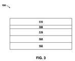
- FIG. 3is a cross section view of the semiconductor structure and illustrates the formation of a fourth semiconductor layer on a thin third semiconductor layer, where the third semiconductor layer is on the porous semiconductor layer, according to an exemplary embodiment
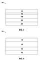
- FIG. 4is a cross section view of an alternative semiconductor structure and illustrates the conversion of the porous semiconductor layer into a buried oxide (BOX) layer, according to an alternative embodiment
- FIG. 5is a cross section view of an alternative semiconductor structure and illustrates the conversion of the porous semiconductor layer and the third semiconductor layer into an alternative buried oxide (BOX) layer, according to an alternative embodiment.
- BOXburied oxide
- references in the specification to “one embodiment”, “an embodiment”, “an example embodiment”, etc.,indicate that the embodiment described may include a particular feature, structure, or characteristic, but every embodiment may not necessarily include the particular feature, structure, or characteristic. Moreover, such phrases are not necessarily referring to the same embodiment. Further, when a particular feature, structure, or characteristic is described in connection with an embodiment, it is submitted that it is within the knowledge of one skilled in the art to affect such feature, structure, or characteristic in connection with other embodiments whether or not explicitly described.
- the terms “upper”, “lower”, “right”, “left”, “vertical”, “horizontal”, “top”, “bottom”, and derivatives thereofshall relate to the disclosed structures and methods, as oriented in the drawing figures.
- the terms “overlying”, “atop”, “on top”, “positioned on” or “positioned atop”mean that a first element, such as a first structure, is present on a second element, such as a second structure, wherein intervening elements, such as an interface structure may be present between the first element and the second element.
- the term “direct contact”means that a first element, such as a first structure, and a second element, such as a second structure, are connected without any intermediary conducting, insulating or semiconductor layers at the interface of the two elements.
- the present inventiongenerally relates to semiconductor device manufacturing, and more particularly to the formation of a porous silicon structure.
- One way to fabricate a III-V semiconductor on a silicon substrateis to use a porous silicon structure to elastically compensate for the lattice mismatch between a substrate and a III-V semiconductor.
- One embodiment by which to form a III-V semiconductor on a porous silicon structureis described in detail below referring to the accompanying drawings FIGS. 1-5 .
- FIG. 1a demonstrative illustration of a structure 100 is provided during an intermediate step of a method of fabricating a semiconductor layer on a porous silicon structure according to an embodiment. More specifically, the method can start by forming a stack 101 .
- the stack 101may include (from bottom to top) a substrate 102 , a first semiconductor layer 104 , a second semiconductor layer 106 , and a third semiconductor layer 108 .
- the stack 101may be formed in a similar fashion to a typical semiconductor-on-insulator (SOI); however, the stack 101 may subsequently include a porous layer with the ability to act as a stress compensator for any lattice mismatch between varying materials.
- SOIsemiconductor-on-insulator
- the substrate 102may include; a bulk semiconductor substrate, a layered semiconductor substrate (e.g., Si/SiGe), a silicon-on-insulator substrate (SOI), or a SiGe-on-insulator substrate (SGOI).
- the substrate 102may include any semiconductor material known in the art, such as, for example; Si, Ge, SiGe, SiC, SiGeC, Ga, GaAs, InAs, InP, or other elemental or compound semiconductors.
- the substrate 102may include, for example; an n-type, p-type, or undoped semiconductor material and may have a monocrystalline, polycrystalline, or amorphous structure. In an embodiment, the substrate 102 is highly p-doped silicon having a ⁇ 100> crystallographic orientation.
- the first semiconductor layer 104may be formed on the substrate 102 using any deposition technique known in the art, such as, for example, epitaxial growth, chemical vapor deposition (CVD), physical vapor deposition (PVD), or atomic layer deposition (ALD).
- the first semiconductor layer 104can be any semiconductor material known in the art, such as, for example, silicon or SiGe.
- the first semiconductor layer 104is silicon with a boron dopant concentration of about 2E18 cm ⁇ 3 (i.e., 2 ⁇ 10 18 atoms per centimeter cubed) and a thickness of about 1000 ⁇ .
- the first semiconductor layer 104may be referred to as having a “low doping concentration” relative to subsequently formed layers.
- the first semiconductor layer 104may be referred to as a base semiconductor layer or a base silicon layer.
- the second semiconductor layer 106may be formed on the first semiconductor layer 104 using any deposition technique known in the art, such as, for example, epitaxial growth, chemical vapor deposition (CVD), physical vapor deposition (PVD), or atomic layer deposition (ALD).
- the second semiconductor layer 106can be any semiconductor material known in the art, such as, for example, silicon or SiGe.
- the second semiconductor layer 106may have a thickness ranging from about 100 nm to about 200 nm; however, other thicknesses may be used.
- the second semiconductor layer 106is a thick silicon layer grown on the first semiconductor layer 104 using epitaxy, where the second semiconductor layer 106 has a boron dopant concentration of about 2E20 cm ⁇ 3 (i.e., 2 ⁇ 10 20 atoms per centimeter cubed) and a thickness of about 150 nm.
- the second semiconductor layer 106may be referred to as “highly doped” relative to other layers, such as, for example, the first semiconductor layer 104 .
- the high doping of the second semiconductor layer 106may help with porousification performed in subsequent steps, both with forming the pores and with making the pores relatively large.
- the second semiconductor layer 106may be referred to as a relaxed second semiconductor layer or a thick semiconductor layer.
- the third semiconductor layer 108may be formed on the second semiconductor layer 106 using any deposition technique known in the art, such as, for example, epitaxial growth, chemical vapor deposition (CVD), physical vapor deposition (PVD), or atomic layer deposition (ALD).
- the third semiconductor layer 108can be any semiconductor material known in the art, such as, for example, silicon or SiGe.
- the third semiconductor layer 108may have a thickness ranging from about 10 nm to about 50 nm; however, other thicknesses may be used.
- the third semiconductor layer 108may be formed on the second semiconductor layer 106 before the second semiconductor layer 106 undergoes the above mentioned porousification step (described in detail below with reference to FIG. 2 ).
- the third semiconductor layer 108is a thin silicon layer grown on the second semiconductor layer 106 using epitaxy, where the third semiconductor layer 108 has a boron dopant concentration of about 2E18 cm ⁇ 3 (i.e., 2 ⁇ 10 18 atoms per centimeter cubed).
- the third semiconductor layer 108may be referred to as having a “low doping concentration” relative to other layers, such as, for example, the second semiconductor layer 106 .
- the third semiconductor layer 108may be referred to as a relaxed third semiconductor layer or a thin semiconductor layer.
- a demonstrative illustration of the structure 100is provided during an intermediate step of a method of fabricating a semiconductor layer on a porous silicon structure according to an embodiment. More specifically, the method can include converting the second semiconductor layer 106 into a porous semiconductor layer 116 .
- the second semiconductor layer 106may be converted into the porous semiconductor layer 116 using any porousification technique know in the art, such as, for example, anodization.
- an anodization processthe structure 100 may be immersed into a hydrofluoric fluoride (HF) bath while applying an electrical bias to the structure 100 , where the HF bath reacts with the second semiconductor layer 106 (e.g., because of the highly doped material of the second semiconductor layer 106 ) forming pores in the second semiconductor layer 106 and converting the second semiconductor layer 106 into the porous semiconductor layer 116 .
- HFhydrofluoric fluoride
- One benefit of having the third semiconductor layer 108may include providing a uniform current flow during the anodization process due to the low doping concentration.
- the HF anodizationconverts p-doped single crystal silicon into porous silicon.
- the rate of formation and the nature of the porous silicon so-formedis determined by both the material properties (i.e., doping type and concentration) as well as the reaction conditions of the anodization process itself (current density, bias, illumination and additives in the HF-containing solution). More specifically, the porous silicon forms with greatly increased efficiency in the higher doped regions and therefore, the second semiconductor layer 106 is efficiently converted into the porous semiconductor layer 116 .
- HF-containing solutionor “HF bath” may include concentrated HF (49%), a mixture of HF and water, a mixture of HF and a monohydric alcohol such as methanol, ethanol, propanol, etc, or HF mixed with at least one surfactant.
- the amount of surfactant that is present in the HF solutionis typically from about 1% to about 50%, based on 49% HF.
- the porousification processis followed up with a conventional hydrogen (H 2 ) anneal process that: (i) removes the light boron doping in the third semiconductor layer 108 ; (ii) closes small pores in the third semiconductor layer 108 ; and (iii) does not affect the relatively large pores formed in porous semiconductor layer 116 .
- H 2hydrogen
- a demonstrative illustration of the structure 100is provided during an intermediate step of a method of fabricating a semiconductor layer on a porous silicon structure according to an embodiment. More specifically, the method can include forming a forth semiconductor layer 110 on the third semiconductor layer 108 .
- the forth semiconductor layer 110may be formed on the third semiconductor layer 108 using any deposition technique known in the art, such as, for example, epitaxial growth, chemical vapor deposition (CVD), physical vapor deposition (PVD), or atomic layer deposition (ALD).
- the forth semiconductor layer 110may have a thickness ranging from about 500 nm to about 1 ⁇ m; however, other thicknesses may be used.
- the forth semiconductor layer 110is a III-V semiconductor with a thickness of about 100 nm.
- the III-V semiconductorwhen a III-V semiconductor is grown on a silicon seed layer, the III-V semiconductor may be forced to match the lattice structure of the seed layer because of the large lattice mismatch between silicon (5.4 ⁇ ) and III-V semiconductor (5.6 ⁇ -6.4 ⁇ ). Therefore, the III-V semiconductor may be under stress and misfit dislocations or defects may form between the seed layer and a critical thickness of the III-V semiconductor, at which time the III-V semiconductor may relax.
- the porous semiconductor layer 116may be soft and may accommodate the high lattice mismatch between the fourth semiconductor layer 110 (e.g., a III-V semiconductor) and the third semiconductor layer 108 (e.g., a silicon seed layer).
- the porous semiconductor layer 116may compensate for stress due to the lattice mismatch because the third semiconductor layer 108 (on top of the porous semiconductor layer 116 ) may have a relatively thin thickness.
- the thin third semiconductor layer 108may stretch to match the lattice structure of the fourth semiconductor layer 110 , where the porous semiconductor layer 116 can allow for stretching of the third semiconductor layer 108 because of the porous characteristics described above.
- the fourth semiconductor layer 110may be formed in a relaxed state (e.g., low defects) because of the stress consumed by the third semiconductor layer 108 facilitated by the porous semiconductor layer 116 .
- a separate pFET devicecan be a silicon fin formed on the same silicon seed layer (i.e., the third semiconductor layer 108 ) and adjacent to the fourth semiconductor layer 110 , such that the similar lattice structure will not stretch the third semiconductor layer 108 beneath the silicon fin.
- a demonstrative illustration of a structure 200is provided during an intermediate step of a method of fabricating a semiconductor layer on a porous silicon structure according to an alternative embodiment.
- the structure 200may be substantially similar in all respect to the structure 100 , described above, and undergo additional processing. More specifically, the method can further include converting the porous semiconductor layer 116 into a buried oxide (BOX) layer 216 .
- BOXburied oxide
- the porous semiconductor layer 116may be converted into the BOX layer 216 using any oxidation technique known in the art, such as, for example, dry oxidation.
- the oxidationmay convert the porous semiconductor layer 116 only because of the porous characteristics described above.
- Thermal oxidationmay be performed in a dry oxidizing ambient atmosphere and at a temperature ranging from about 750° C. to about 1100° C. to convert the porous layer 116 into the BOX layer 216 .
- the structure 200may include the fourth semiconductor layer 110 on the third semiconductor layer 108 , where the third semiconductor layer 108 is on the BOX layer 216 .
- a demonstrative illustration of a structure 300is provided during an intermediate step of a method of fabricating a semiconductor layer on a porous silicon structure according to an embodiment.
- the structure 300may be substantially similar in all respect to the structure 100 , described above, and undergo additional processing. More specifically, the method can include converting both the porous semiconductor layer 116 and the third semiconductor layer 108 into a buried oxide layer (BOX) 316 .
- BOXburied oxide layer
- the porous semiconductor layer 116 and the third semiconductor layer 108may both be converted into the BOX layer 316 using any oxidation technique known in the art, such as, for example, dry oxidation.
- the alternative structure 300may include the fourth semiconductor layer 110 directly on the BOX layer 316 .
Landscapes
- Engineering & Computer Science (AREA)
- Physics & Mathematics (AREA)
- Condensed Matter Physics & Semiconductors (AREA)
- General Physics & Mathematics (AREA)
- Manufacturing & Machinery (AREA)
- Computer Hardware Design (AREA)
- Microelectronics & Electronic Packaging (AREA)
- Power Engineering (AREA)
- Chemical & Material Sciences (AREA)
- Crystallography & Structural Chemistry (AREA)
- Recrystallisation Techniques (AREA)
Abstract
Description
Claims (12)
Priority Applications (2)
| Application Number | Priority Date | Filing Date | Title |
|---|---|---|---|
| US14/645,449US10032870B2 (en) | 2015-03-12 | 2015-03-12 | Low defect III-V semiconductor template on porous silicon |
| US16/018,304US20190043956A1 (en) | 2015-03-12 | 2018-06-26 | Low defect iii-v semiconductor template on porous silicon |
Applications Claiming Priority (1)
| Application Number | Priority Date | Filing Date | Title |
|---|---|---|---|
| US14/645,449US10032870B2 (en) | 2015-03-12 | 2015-03-12 | Low defect III-V semiconductor template on porous silicon |
Related Child Applications (1)
| Application Number | Title | Priority Date | Filing Date |
|---|---|---|---|
| US16/018,304DivisionUS20190043956A1 (en) | 2015-03-12 | 2018-06-26 | Low defect iii-v semiconductor template on porous silicon |
Publications (2)
| Publication Number | Publication Date |
|---|---|
| US20160268123A1 US20160268123A1 (en) | 2016-09-15 |
| US10032870B2true US10032870B2 (en) | 2018-07-24 |
Family
ID=56887963
Family Applications (2)
| Application Number | Title | Priority Date | Filing Date |
|---|---|---|---|
| US14/645,449Expired - Fee RelatedUS10032870B2 (en) | 2015-03-12 | 2015-03-12 | Low defect III-V semiconductor template on porous silicon |
| US16/018,304AbandonedUS20190043956A1 (en) | 2015-03-12 | 2018-06-26 | Low defect iii-v semiconductor template on porous silicon |
Family Applications After (1)
| Application Number | Title | Priority Date | Filing Date |
|---|---|---|---|
| US16/018,304AbandonedUS20190043956A1 (en) | 2015-03-12 | 2018-06-26 | Low defect iii-v semiconductor template on porous silicon |
Country Status (1)
| Country | Link |
|---|---|
| US (2) | US10032870B2 (en) |
Cited By (1)
| Publication number | Priority date | Publication date | Assignee | Title |
|---|---|---|---|---|
| US20160359044A1 (en)* | 2015-06-04 | 2016-12-08 | International Business Machines Corporation | FORMATION OF DISLOCATION-FREE SiGe FINFET USING POROUS SILICON |
Families Citing this family (6)
| Publication number | Priority date | Publication date | Assignee | Title |
|---|---|---|---|---|
| US10453683B2 (en)* | 2017-03-23 | 2019-10-22 | International Business Machines Corporation | Post growth heteroepitaxial layer separation for defect reduction in heteroepitaxial films |
| US10741452B2 (en)* | 2018-10-29 | 2020-08-11 | International Business Machines Corporation | Controlling fin hardmask cut profile using a sacrificial epitaxial structure |
| US11355340B2 (en)* | 2019-07-19 | 2022-06-07 | Iqe Plc | Semiconductor material having tunable permittivity and tunable thermal conductivity |
| US20240063340A1 (en)* | 2019-09-10 | 2024-02-22 | The Regents Of The University Of California | METHOD FOR RELAXING SEMICONDUCTOR FILMS INCLUDING THE FABRICATION OF PSEUDO-SUBSTRATES AND FORMATION OF COMPOSITES ALLOWING THE ADDITION OF PREVIOUSLY UN-ACCESSIBLE FUNCTIONALITY OF GROUP lll-NITRIDES |
| DE102020103197A1 (en) | 2020-02-07 | 2021-08-12 | Fraunhofer-Gesellschaft zur Förderung der angewandten Forschung eingetragener Verein | Semiconductor structure for a semiconductor component and method for producing such a semiconductor structure |
| DE102020119953A1 (en)* | 2020-07-29 | 2022-02-03 | Infineon Technologies Ag | Method of forming a semiconductor device |
Citations (47)
| Publication number | Priority date | Publication date | Assignee | Title |
|---|---|---|---|---|
| US4806996A (en) | 1986-04-10 | 1989-02-21 | American Telephone And Telegraph Company, At&T Bell Laboratories | Dislocation-free epitaxial layer on a lattice-mismatched porous or otherwise submicron patterned single crystal substrate |
| US4982263A (en)* | 1987-12-21 | 1991-01-01 | Texas Instruments Incorporated | Anodizable strain layer for SOI semiconductor structures |
| US5439843A (en)* | 1992-01-31 | 1995-08-08 | Canon Kabushiki Kaisha | Method for preparing a semiconductor substrate using porous silicon |
| US5950094A (en)* | 1999-02-18 | 1999-09-07 | Taiwan Semiconductor Manufacturing Company, Ltd. | Method for fabricating fully dielectric isolated silicon (FDIS) |
| US6107213A (en)* | 1996-02-01 | 2000-08-22 | Sony Corporation | Method for making thin film semiconductor |
| US6106613A (en)* | 1997-03-17 | 2000-08-22 | Canon Kabushiki Kaisha | Semiconductor substrate having compound semiconductor layer, process for its production, and electronic device fabricated on semiconductor substrate |
| US6143628A (en)* | 1997-03-27 | 2000-11-07 | Canon Kabushiki Kaisha | Semiconductor substrate and method of manufacturing the same |
| US6344375B1 (en)* | 1998-07-28 | 2002-02-05 | Matsushita Electric Industrial Co., Ltd | Substrate containing compound semiconductor, method for manufacturing the same and semiconductor device using the same |
| US6407441B1 (en)* | 1997-12-29 | 2002-06-18 | Texas Instruments Incorporated | Integrated circuit and method of using porous silicon to achieve component isolation in radio frequency applications |
| US6417069B1 (en)* | 1999-03-25 | 2002-07-09 | Canon Kabushiki Kaisha | Substrate processing method and manufacturing method, and anodizing apparatus |
| US6486917B2 (en)* | 2000-01-27 | 2002-11-26 | Sony Corporation | Image-pickup apparatus, fabrication method thereof, and camera system |
| US6534382B1 (en)* | 1996-12-18 | 2003-03-18 | Canon Kabushiki Kaisha | Process for producing semiconductor article |
| US6593211B2 (en) | 1998-09-04 | 2003-07-15 | Canon Kabushiki Kaisha | Semiconductor substrate and method for producing the same |
| US6602767B2 (en)* | 2000-01-27 | 2003-08-05 | Canon Kabushiki Kaisha | Method for transferring porous layer, method for making semiconductor devices, and method for making solar battery |
| US6602760B2 (en)* | 2000-12-21 | 2003-08-05 | Interuniversitair Microelektronica Centrum (Imec) | Method of producing a semiconductor layer on a substrate |
| US20030205480A1 (en)* | 1998-02-26 | 2003-11-06 | Kiyofumi Sakaguchi | Anodizing method and apparatus and semiconductor substrate manufacturing method |
| US6794805B1 (en)* | 1998-05-26 | 2004-09-21 | Matsushita Electric Works, Ltd. | Field emission electron source, method of producing the same, and use of the same |
| US6881650B2 (en) | 2001-12-03 | 2005-04-19 | Samsung Electronics Co., Ltd. | Method for forming SOI substrate |
| US6921914B2 (en) | 2000-08-16 | 2005-07-26 | Massachusetts Institute Of Technology | Process for producing semiconductor article using graded epitaxial growth |
| US7060597B2 (en) | 2003-05-19 | 2006-06-13 | Toshiba Ceramics Co., Ltd. | Manufacturing method for a silicon substrate having strained layer |
| US7095043B2 (en) | 2003-06-18 | 2006-08-22 | Hitachi, Ltd. | Semiconductor device, semiconductor circuit module and manufacturing method of the same |
| US7125458B2 (en) | 2003-09-12 | 2006-10-24 | International Business Machines Corporation | Formation of a silicon germanium-on-insulator structure by oxidation of a buried porous silicon layer |
| US7157352B2 (en)* | 2002-10-11 | 2007-01-02 | Sony Corporation | Method for producing ultra-thin semiconductor device |
| US7327036B2 (en)* | 2003-12-22 | 2008-02-05 | Interuniversitair Microelektronica Centrum (Imec) | Method for depositing a group III-nitride material on a silicon substrate and device therefor |
| US7365399B2 (en)* | 2006-01-17 | 2008-04-29 | International Business Machines Corporation | Structure and method to form semiconductor-on-pores (SOP) for high device performance and low manufacturing cost |
| US20080171424A1 (en)* | 2007-01-16 | 2008-07-17 | Sharp Laboratories Of America, Inc. | Epitaxial growth of GaN and SiC on silicon using nanowires and nanosize nucleus methodologies |
| US7410883B2 (en)* | 2005-04-13 | 2008-08-12 | Corning Incorporated | Glass-based semiconductor on insulator structures and methods of making same |
| US7420201B2 (en)* | 2002-06-07 | 2008-09-02 | Amberwave Systems Corporation | Strained-semiconductor-on-insulator device structures with elevated source/drain regions |
| US7553369B2 (en)* | 2002-05-07 | 2009-06-30 | Universite Claude Bernard Lyon 1 | Method of altering the properties of a thin film and substrate implementing said method |
| US20090217967A1 (en)* | 2008-02-29 | 2009-09-03 | International Business Machines Corporation | Porous silicon quantum dot photodetector |
| US7772096B2 (en)* | 2008-07-10 | 2010-08-10 | International Machines Corporation | Formation of SOI by oxidation of silicon with engineered porosity gradient |
| US7833884B2 (en)* | 2007-11-02 | 2010-11-16 | International Business Machines Corporation | Strained semiconductor-on-insulator by Si:C combined with porous process |
| US20110057295A1 (en)* | 2005-09-30 | 2011-03-10 | Osram Opto Semiconductors Gmbh | Epitaxial substrate component made therewith and corresponding production method |
| US7928436B2 (en) | 2005-10-26 | 2011-04-19 | International Business Machines Corporation | Methods for forming germanium-on-insulator semiconductor structures using a porous layer and semiconductor structures formed by these methods |
| US8157978B2 (en)* | 2009-01-29 | 2012-04-17 | International Business Machines Corporation | Etching system and method for forming multiple porous semiconductor regions with different optical and structural properties on a single semiconductor wafer |
| US8304810B2 (en) | 1999-03-30 | 2012-11-06 | Renesas Electronics Corporation | Semiconductor device and semiconductor substrate having selectively etched portions filled with silicon germanium |
| US20130000715A1 (en)* | 2011-03-28 | 2013-01-03 | Solexel, Inc. | Active backplane for thin silicon solar cells |
| US20130337601A1 (en)* | 2012-02-29 | 2013-12-19 | Solexel, Inc. | Structures and methods for high efficiency compound semiconductor solar cells |
| US8722526B2 (en)* | 2012-07-27 | 2014-05-13 | Veeco Ald Inc. | Growing of gallium-nitrade layer on silicon substrate |
| US8791502B2 (en) | 2011-10-09 | 2014-07-29 | The Institute of Microelectronics Chinese Academy of Science | Semiconductor device and method of manufacturing the same |
| US8815618B2 (en)* | 2008-08-29 | 2014-08-26 | Tsmc Solid State Lighting Ltd. | Light-emitting diode on a conductive substrate |
| US9012253B2 (en)* | 2009-12-16 | 2015-04-21 | Micron Technology, Inc. | Gallium nitride wafer substrate for solid state lighting devices, and associated systems and methods |
| US9093271B2 (en)* | 2011-06-30 | 2015-07-28 | Soitec | Method for manufacturing a thick epitaxial layer of gallium nitride on a silicon or similar substrate and layer obtained using said method |
| US20150270120A1 (en)* | 2014-03-20 | 2015-09-24 | Wei-E Wang | Methods of forming low-defect strain-relaxed layers on lattice-mismatched substrates and related semiconductor structures and devices |
| US9198294B2 (en)* | 2010-11-19 | 2015-11-24 | Soitec | Electronic device for radiofrequency or power applications and process for manufacturing such a device |
| US9224904B1 (en)* | 2011-07-24 | 2015-12-29 | Ananda Kumar | Composite substrates of silicon and ceramic |
| US20160190302A1 (en)* | 2014-12-30 | 2016-06-30 | Globalfoundries Inc. | Soi based finfet with strained source-drain regions |
Family Cites Families (6)
| Publication number | Priority date | Publication date | Assignee | Title |
|---|---|---|---|---|
| JPH08148280A (en)* | 1994-04-14 | 1996-06-07 | Toshiba Corp | Semiconductor device and manufacturing method thereof |
| US20090001416A1 (en)* | 2007-06-28 | 2009-01-01 | National University Of Singapore | Growth of indium gallium nitride (InGaN) on porous gallium nitride (GaN) template by metal-organic chemical vapor deposition (MOCVD) |
| JP5961557B2 (en)* | 2010-01-27 | 2016-08-02 | イェイル ユニヴァーシティ | Conductivity-based selective etching for GaN devices and applications thereof |
| WO2014179523A2 (en)* | 2013-05-01 | 2014-11-06 | Sensor Electronic Technology, Inc. | Stress relieving semiconductor layer |
| CN105556680B (en)* | 2013-05-22 | 2017-12-22 | 王士原 | Microstructure-enhanced absorption photosensitive device |
| US9412902B2 (en)* | 2014-02-22 | 2016-08-09 | Sensor Electronic Technology, Inc. | Semiconductor structure with stress-reducing buffer structure |
- 2015
- 2015-03-12USUS14/645,449patent/US10032870B2/ennot_activeExpired - Fee Related
- 2018
- 2018-06-26USUS16/018,304patent/US20190043956A1/ennot_activeAbandoned
Patent Citations (48)
| Publication number | Priority date | Publication date | Assignee | Title |
|---|---|---|---|---|
| US4806996A (en) | 1986-04-10 | 1989-02-21 | American Telephone And Telegraph Company, At&T Bell Laboratories | Dislocation-free epitaxial layer on a lattice-mismatched porous or otherwise submicron patterned single crystal substrate |
| US4982263A (en)* | 1987-12-21 | 1991-01-01 | Texas Instruments Incorporated | Anodizable strain layer for SOI semiconductor structures |
| US5439843A (en)* | 1992-01-31 | 1995-08-08 | Canon Kabushiki Kaisha | Method for preparing a semiconductor substrate using porous silicon |
| US6107213A (en)* | 1996-02-01 | 2000-08-22 | Sony Corporation | Method for making thin film semiconductor |
| US6194239B1 (en)* | 1996-02-01 | 2001-02-27 | Sony Corporation | Method for making thin film semiconductor |
| US6534382B1 (en)* | 1996-12-18 | 2003-03-18 | Canon Kabushiki Kaisha | Process for producing semiconductor article |
| US6106613A (en)* | 1997-03-17 | 2000-08-22 | Canon Kabushiki Kaisha | Semiconductor substrate having compound semiconductor layer, process for its production, and electronic device fabricated on semiconductor substrate |
| US6143628A (en)* | 1997-03-27 | 2000-11-07 | Canon Kabushiki Kaisha | Semiconductor substrate and method of manufacturing the same |
| US6407441B1 (en)* | 1997-12-29 | 2002-06-18 | Texas Instruments Incorporated | Integrated circuit and method of using porous silicon to achieve component isolation in radio frequency applications |
| US20030205480A1 (en)* | 1998-02-26 | 2003-11-06 | Kiyofumi Sakaguchi | Anodizing method and apparatus and semiconductor substrate manufacturing method |
| US6794805B1 (en)* | 1998-05-26 | 2004-09-21 | Matsushita Electric Works, Ltd. | Field emission electron source, method of producing the same, and use of the same |
| US6344375B1 (en)* | 1998-07-28 | 2002-02-05 | Matsushita Electric Industrial Co., Ltd | Substrate containing compound semiconductor, method for manufacturing the same and semiconductor device using the same |
| US6593211B2 (en) | 1998-09-04 | 2003-07-15 | Canon Kabushiki Kaisha | Semiconductor substrate and method for producing the same |
| US5950094A (en)* | 1999-02-18 | 1999-09-07 | Taiwan Semiconductor Manufacturing Company, Ltd. | Method for fabricating fully dielectric isolated silicon (FDIS) |
| US6417069B1 (en)* | 1999-03-25 | 2002-07-09 | Canon Kabushiki Kaisha | Substrate processing method and manufacturing method, and anodizing apparatus |
| US8304810B2 (en) | 1999-03-30 | 2012-11-06 | Renesas Electronics Corporation | Semiconductor device and semiconductor substrate having selectively etched portions filled with silicon germanium |
| US6602767B2 (en)* | 2000-01-27 | 2003-08-05 | Canon Kabushiki Kaisha | Method for transferring porous layer, method for making semiconductor devices, and method for making solar battery |
| US6486917B2 (en)* | 2000-01-27 | 2002-11-26 | Sony Corporation | Image-pickup apparatus, fabrication method thereof, and camera system |
| US6921914B2 (en) | 2000-08-16 | 2005-07-26 | Massachusetts Institute Of Technology | Process for producing semiconductor article using graded epitaxial growth |
| US6602760B2 (en)* | 2000-12-21 | 2003-08-05 | Interuniversitair Microelektronica Centrum (Imec) | Method of producing a semiconductor layer on a substrate |
| US6881650B2 (en) | 2001-12-03 | 2005-04-19 | Samsung Electronics Co., Ltd. | Method for forming SOI substrate |
| US7553369B2 (en)* | 2002-05-07 | 2009-06-30 | Universite Claude Bernard Lyon 1 | Method of altering the properties of a thin film and substrate implementing said method |
| US7420201B2 (en)* | 2002-06-07 | 2008-09-02 | Amberwave Systems Corporation | Strained-semiconductor-on-insulator device structures with elevated source/drain regions |
| US7157352B2 (en)* | 2002-10-11 | 2007-01-02 | Sony Corporation | Method for producing ultra-thin semiconductor device |
| US7060597B2 (en) | 2003-05-19 | 2006-06-13 | Toshiba Ceramics Co., Ltd. | Manufacturing method for a silicon substrate having strained layer |
| US7095043B2 (en) | 2003-06-18 | 2006-08-22 | Hitachi, Ltd. | Semiconductor device, semiconductor circuit module and manufacturing method of the same |
| US7125458B2 (en) | 2003-09-12 | 2006-10-24 | International Business Machines Corporation | Formation of a silicon germanium-on-insulator structure by oxidation of a buried porous silicon layer |
| US7327036B2 (en)* | 2003-12-22 | 2008-02-05 | Interuniversitair Microelektronica Centrum (Imec) | Method for depositing a group III-nitride material on a silicon substrate and device therefor |
| US7410883B2 (en)* | 2005-04-13 | 2008-08-12 | Corning Incorporated | Glass-based semiconductor on insulator structures and methods of making same |
| US20110057295A1 (en)* | 2005-09-30 | 2011-03-10 | Osram Opto Semiconductors Gmbh | Epitaxial substrate component made therewith and corresponding production method |
| US7928436B2 (en) | 2005-10-26 | 2011-04-19 | International Business Machines Corporation | Methods for forming germanium-on-insulator semiconductor structures using a porous layer and semiconductor structures formed by these methods |
| US7365399B2 (en)* | 2006-01-17 | 2008-04-29 | International Business Machines Corporation | Structure and method to form semiconductor-on-pores (SOP) for high device performance and low manufacturing cost |
| US20080171424A1 (en)* | 2007-01-16 | 2008-07-17 | Sharp Laboratories Of America, Inc. | Epitaxial growth of GaN and SiC on silicon using nanowires and nanosize nucleus methodologies |
| US7833884B2 (en)* | 2007-11-02 | 2010-11-16 | International Business Machines Corporation | Strained semiconductor-on-insulator by Si:C combined with porous process |
| US20090217967A1 (en)* | 2008-02-29 | 2009-09-03 | International Business Machines Corporation | Porous silicon quantum dot photodetector |
| US7772096B2 (en)* | 2008-07-10 | 2010-08-10 | International Machines Corporation | Formation of SOI by oxidation of silicon with engineered porosity gradient |
| US8815618B2 (en)* | 2008-08-29 | 2014-08-26 | Tsmc Solid State Lighting Ltd. | Light-emitting diode on a conductive substrate |
| US8157978B2 (en)* | 2009-01-29 | 2012-04-17 | International Business Machines Corporation | Etching system and method for forming multiple porous semiconductor regions with different optical and structural properties on a single semiconductor wafer |
| US9012253B2 (en)* | 2009-12-16 | 2015-04-21 | Micron Technology, Inc. | Gallium nitride wafer substrate for solid state lighting devices, and associated systems and methods |
| US9198294B2 (en)* | 2010-11-19 | 2015-11-24 | Soitec | Electronic device for radiofrequency or power applications and process for manufacturing such a device |
| US20130000715A1 (en)* | 2011-03-28 | 2013-01-03 | Solexel, Inc. | Active backplane for thin silicon solar cells |
| US9093271B2 (en)* | 2011-06-30 | 2015-07-28 | Soitec | Method for manufacturing a thick epitaxial layer of gallium nitride on a silicon or similar substrate and layer obtained using said method |
| US9224904B1 (en)* | 2011-07-24 | 2015-12-29 | Ananda Kumar | Composite substrates of silicon and ceramic |
| US8791502B2 (en) | 2011-10-09 | 2014-07-29 | The Institute of Microelectronics Chinese Academy of Science | Semiconductor device and method of manufacturing the same |
| US20130337601A1 (en)* | 2012-02-29 | 2013-12-19 | Solexel, Inc. | Structures and methods for high efficiency compound semiconductor solar cells |
| US8722526B2 (en)* | 2012-07-27 | 2014-05-13 | Veeco Ald Inc. | Growing of gallium-nitrade layer on silicon substrate |
| US20150270120A1 (en)* | 2014-03-20 | 2015-09-24 | Wei-E Wang | Methods of forming low-defect strain-relaxed layers on lattice-mismatched substrates and related semiconductor structures and devices |
| US20160190302A1 (en)* | 2014-12-30 | 2016-06-30 | Globalfoundries Inc. | Soi based finfet with strained source-drain regions |
Non-Patent Citations (8)
| Title |
|---|
| Boufaden et al., "GaN growth on porous silicon by MOVPE", Microelectronics Journal 34 (2003) pp. 843-848.* |
| Christophersen et al., "Crystal orientation and electrolyte dependence for macropore nucleation and stable growth on p-type Si", Materials Science and Engineering B69-70 (2000) pp. 194-198.* |
| Matoussi et al., "Luminescent properties of GaN films grown on porous silicon substrate", Journal of Luminescence 130 (2010) pp. 399-403.* |
| Matoussi et al., "Porous silicon as an intermediate buffer layer for GaN growth on (100) Si", Microelectronics Journal 32 (2001) pp. 995-998.* |
| Pending U.S. Appl. No. 14/585,742, entitled: "SOI Based FINFET With Strained Source-Drain Regions", filed Dec. 30, 2014. |
| Unagami, "Formation Mechanism of Porous Silicon Layer by Anodization in HF Solution", Journal of Electrochemical Society: Solid-State Science and Technology 127 (1980) pp. 476-483.* |
| Zhang et al., "Porous Silicon Formation and Electropolishing of Silicon by Anodic Polarization in HF Solution", Journal of Electrochemical Society 136 (1989) pp. 1561-1565.* |
| Zhang et al., "Porous Silicon: Morphology and Formation Mechanisms", Modern Aspects of Electrochemistry 39 (2005) pp. 65-133.* |
Cited By (2)
| Publication number | Priority date | Publication date | Assignee | Title |
|---|---|---|---|---|
| US20160359044A1 (en)* | 2015-06-04 | 2016-12-08 | International Business Machines Corporation | FORMATION OF DISLOCATION-FREE SiGe FINFET USING POROUS SILICON |
| US10833175B2 (en)* | 2015-06-04 | 2020-11-10 | International Business Machines Corporation | Formation of dislocation-free SiGe finFET using porous silicon |
Also Published As
| Publication number | Publication date |
|---|---|
| US20160268123A1 (en) | 2016-09-15 |
| US20190043956A1 (en) | 2019-02-07 |
Similar Documents
| Publication | Publication Date | Title |
|---|---|---|
| US10032870B2 (en) | Low defect III-V semiconductor template on porous silicon | |
| US9984872B2 (en) | Fabrication and structures of crystalline material | |
| US10961639B2 (en) | Epitaxial growth of crystalline material | |
| US7550370B2 (en) | Method of forming thin SGOI wafers with high relaxation and low stacking fault defect density | |
| US7202121B2 (en) | Methods for preserving strained semiconductor substrate layers during CMOS processing | |
| US8956453B2 (en) | Method for producing a crystalline germanium layer on a substrate | |
| EP2299475A1 (en) | Improved fabrication and structures of crystalline material | |
| US7750367B2 (en) | Semiconductor member, manufacturing method thereof, and semiconductor device | |
| Yu et al. | p-Channel Ge MOSFET by selectively heteroepitaxially grown Ge on Si | |
| US9627491B2 (en) | Aspect ratio trapping and lattice engineering for III/V semiconductors | |
| US7495266B2 (en) | Strained silicon-on-silicon by wafer bonding and layer transfer | |
| TW580727B (en) | Semiconductor substrate, field effect transistor, and manufacturing method for the same | |
| CN100429761C (en) | Formation of silicon-germanium-on-insulator structures by oxidizing and burying porous silicon layers | |
| US10438858B2 (en) | Low-cost SOI FinFET technology | |
| US9502245B1 (en) | Elimination of defects in long aspect ratio trapping trench structures | |
| US20050280081A1 (en) | Semiconductor devices having bonded interfaces and methods for making the same | |
| Asadollahi et al. | Fabrication of Relaxed Germanium on Insulator via Room Temperature Wafer Bonding | |
| EP2167701A1 (en) | Method for providing a crystalline germanium layer on a substrate |
Legal Events
| Date | Code | Title | Description |
|---|---|---|---|
| AS | Assignment | Owner name:INTERNATIONAL BUSINESS MACHINES CORPORATION, NEW Y Free format text:ASSIGNMENT OF ASSIGNORS INTEREST;ASSIGNORS:DE SOUZA, JOEL P.;FOGEL, KEITH E.;REZNICEK, ALEXANDER;AND OTHERS;REEL/FRAME:035145/0921 Effective date:20150303 | |
| AS | Assignment | Owner name:GLOBALFOUNDRIES U.S. 2 LLC, NEW YORK Free format text:ASSIGNMENT OF ASSIGNORS INTEREST;ASSIGNOR:INTERNATIONAL BUSINESS MACHINES CORPORATION;REEL/FRAME:036550/0001 Effective date:20150629 | |
| AS | Assignment | Owner name:GLOBALFOUNDRIES INC., CAYMAN ISLANDS Free format text:ASSIGNMENT OF ASSIGNORS INTEREST;ASSIGNORS:GLOBALFOUNDRIES U.S. 2 LLC;GLOBALFOUNDRIES U.S. INC.;REEL/FRAME:036779/0001 Effective date:20150910 | |
| STCF | Information on status: patent grant | Free format text:PATENTED CASE | |
| AS | Assignment | Owner name:WILMINGTON TRUST, NATIONAL ASSOCIATION, DELAWARE Free format text:SECURITY AGREEMENT;ASSIGNOR:GLOBALFOUNDRIES INC.;REEL/FRAME:049490/0001 Effective date:20181127 | |
| AS | Assignment | Owner name:GLOBALFOUNDRIES U.S. INC., CALIFORNIA Free format text:ASSIGNMENT OF ASSIGNORS INTEREST;ASSIGNOR:GLOBALFOUNDRIES INC.;REEL/FRAME:054633/0001 Effective date:20201022 | |
| AS | Assignment | Owner name:GLOBALFOUNDRIES INC., CAYMAN ISLANDS Free format text:RELEASE BY SECURED PARTY;ASSIGNOR:WILMINGTON TRUST, NATIONAL ASSOCIATION;REEL/FRAME:054636/0001 Effective date:20201117 | |
| AS | Assignment | Owner name:GLOBALFOUNDRIES U.S. INC., NEW YORK Free format text:RELEASE BY SECURED PARTY;ASSIGNOR:WILMINGTON TRUST, NATIONAL ASSOCIATION;REEL/FRAME:056987/0001 Effective date:20201117 | |
| FEPP | Fee payment procedure | Free format text:MAINTENANCE FEE REMINDER MAILED (ORIGINAL EVENT CODE: REM.); ENTITY STATUS OF PATENT OWNER: LARGE ENTITY | |
| LAPS | Lapse for failure to pay maintenance fees | Free format text:PATENT EXPIRED FOR FAILURE TO PAY MAINTENANCE FEES (ORIGINAL EVENT CODE: EXP.); ENTITY STATUS OF PATENT OWNER: LARGE ENTITY | |
| STCH | Information on status: patent discontinuation | Free format text:PATENT EXPIRED DUE TO NONPAYMENT OF MAINTENANCE FEES UNDER 37 CFR 1.362 | |
| FP | Lapsed due to failure to pay maintenance fee | Effective date:20220724 |