US10032719B2 - Semiconductor device structures - Google Patents
Semiconductor device structuresDownload PDFInfo
- Publication number
- US10032719B2 US10032719B2US15/606,312US201715606312AUS10032719B2US 10032719 B2US10032719 B2US 10032719B2US 201715606312 AUS201715606312 AUS 201715606312AUS 10032719 B2US10032719 B2US 10032719B2
- Authority
- US
- United States
- Prior art keywords
- resist
- features
- substrate
- semiconductor device
- pools
- Prior art date
- Legal status (The legal status is an assumption and is not a legal conclusion. Google has not performed a legal analysis and makes no representation as to the accuracy of the status listed.)
- Active
Links
- 239000004065semiconductorSubstances0.000titleclaimsabstractdescription44
- 239000000758substrateSubstances0.000claimsabstractdescription79
- PXHVJJICTQNCMI-UHFFFAOYSA-NNickelChemical compound[Ni]PXHVJJICTQNCMI-UHFFFAOYSA-N0.000claimsdescription4
- 229910052751metalInorganic materials0.000claimsdescription4
- 239000002184metalSubstances0.000claimsdescription4
- BASFCYQUMIYNBI-UHFFFAOYSA-NplatinumChemical compound[Pt]BASFCYQUMIYNBI-UHFFFAOYSA-N0.000claimsdescription4
- 229910021420polycrystalline siliconInorganic materials0.000claimsdescription3
- 229920005591polysiliconPolymers0.000claimsdescription3
- 229910052721tungstenInorganic materials0.000claimsdescription3
- 239000010937tungstenSubstances0.000claimsdescription3
- -1tungsten nitrideChemical class0.000claimsdescription3
- NRTOMJZYCJJWKI-UHFFFAOYSA-NTitanium nitrideChemical compound[Ti]#NNRTOMJZYCJJWKI-UHFFFAOYSA-N0.000claimsdescription2
- UQZIWOQVLUASCR-UHFFFAOYSA-Nalumane;titaniumChemical compound[AlH3].[Ti]UQZIWOQVLUASCR-UHFFFAOYSA-N0.000claimsdescription2
- PCHJSUWPFVWCPO-UHFFFAOYSA-NgoldChemical compound[Au]PCHJSUWPFVWCPO-UHFFFAOYSA-N0.000claimsdescription2
- 239000010931goldSubstances0.000claimsdescription2
- 229910052737goldInorganic materials0.000claimsdescription2
- 229910052759nickelInorganic materials0.000claimsdescription2
- 229910052697platinumInorganic materials0.000claimsdescription2
- MZLGASXMSKOWSE-UHFFFAOYSA-Ntantalum nitrideChemical compound[Ta]#NMZLGASXMSKOWSE-UHFFFAOYSA-N0.000claimsdescription2
- WFKWXMTUELFFGS-UHFFFAOYSA-NtungstenChemical compound[W]WFKWXMTUELFFGS-UHFFFAOYSA-N0.000claimsdescription2
- 239000000463materialSubstances0.000abstractdescription112
- 238000000034methodMethods0.000abstractdescription45
- 230000002378acidificating effectEffects0.000abstractdescription36
- 239000002253acidSubstances0.000description35
- 238000011161developmentMethods0.000description14
- 235000019647acidic tasteNutrition0.000description12
- 239000003960organic solventSubstances0.000description9
- 239000000126substanceSubstances0.000description9
- 238000012545processingMethods0.000description6
- 230000015572biosynthetic processEffects0.000description5
- 238000007796conventional methodMethods0.000description5
- 238000009792diffusion processMethods0.000description4
- 238000005530etchingMethods0.000description4
- 238000004519manufacturing processMethods0.000description4
- 229920002120photoresistant polymerPolymers0.000description4
- XUIMIQQOPSSXEZ-UHFFFAOYSA-NSiliconChemical compound[Si]XUIMIQQOPSSXEZ-UHFFFAOYSA-N0.000description3
- 238000000231atomic layer depositionMethods0.000description3
- 230000003247decreasing effectEffects0.000description3
- 230000005855radiationEffects0.000description3
- 229910052710siliconInorganic materials0.000description3
- 239000010703siliconSubstances0.000description3
- ARXJGSRGQADJSQ-UHFFFAOYSA-N1-methoxypropan-2-olChemical compoundCOCC(C)OARXJGSRGQADJSQ-UHFFFAOYSA-N0.000description2
- CERQOIWHTDAKMF-UHFFFAOYSA-MMethacrylateChemical compoundCC(=C)C([O-])=OCERQOIWHTDAKMF-UHFFFAOYSA-M0.000description2
- 230000003213activating effectEffects0.000description2
- 239000006117anti-reflective coatingSubstances0.000description2
- 238000005229chemical vapour depositionMethods0.000description2
- 239000004020conductorSubstances0.000description2
- JHIVVAPYMSGYDF-UHFFFAOYSA-NcyclohexanoneChemical compoundO=C1CCCCC1JHIVVAPYMSGYDF-UHFFFAOYSA-N0.000description2
- 238000010438heat treatmentMethods0.000description2
- 238000012986modificationMethods0.000description2
- 230000004048modificationEffects0.000description2
- JRZJOMJEPLMPRA-UHFFFAOYSA-NolefinNatural productsCCCCCCCC=CJRZJOMJEPLMPRA-UHFFFAOYSA-N0.000description2
- 230000000737periodic effectEffects0.000description2
- 238000000206photolithographyMethods0.000description2
- 238000005240physical vapour depositionMethods0.000description2
- LLHKCFNBLRBOGN-UHFFFAOYSA-Npropylene glycol methyl ether acetateChemical compoundCOCC(C)OC(C)=OLLHKCFNBLRBOGN-UHFFFAOYSA-N0.000description2
- 238000004528spin coatingMethods0.000description2
- JBRZTFJDHDCESZ-UHFFFAOYSA-NAsGaChemical compound[As]#[Ga]JBRZTFJDHDCESZ-UHFFFAOYSA-N0.000description1
- LFQSCWFLJHTTHZ-UHFFFAOYSA-NEthanolChemical compoundCCOLFQSCWFLJHTTHZ-UHFFFAOYSA-N0.000description1
- 229910002601GaNInorganic materials0.000description1
- 229910001218Gallium arsenideInorganic materials0.000description1
- JMASRVWKEDWRBT-UHFFFAOYSA-NGallium nitrideChemical compound[Ga]#NJMASRVWKEDWRBT-UHFFFAOYSA-N0.000description1
- GPXJNWSHGFTCBW-UHFFFAOYSA-NIndium phosphideChemical compound[In]#PGPXJNWSHGFTCBW-UHFFFAOYSA-N0.000description1
- 229910000577Silicon-germaniumInorganic materials0.000description1
- LEVVHYCKPQWKOP-UHFFFAOYSA-N[Si].[Ge]Chemical compound[Si].[Ge]LEVVHYCKPQWKOP-UHFFFAOYSA-N0.000description1
- 238000003491arrayMethods0.000description1
- IVHJCRXBQPGLOV-UHFFFAOYSA-NazanylidynetungstenChemical compound[W]#NIVHJCRXBQPGLOV-UHFFFAOYSA-N0.000description1
- 230000015556catabolic processEffects0.000description1
- 238000006555catalytic reactionMethods0.000description1
- 239000011248coating agentSubstances0.000description1
- 238000000576coating methodMethods0.000description1
- 238000010276constructionMethods0.000description1
- 238000006731degradation reactionMethods0.000description1
- 238000000151depositionMethods0.000description1
- 238000013461designMethods0.000description1
- 229910052732germaniumInorganic materials0.000description1
- GNPVGFCGXDBREM-UHFFFAOYSA-Ngermanium atomChemical compound[Ge]GNPVGFCGXDBREM-UHFFFAOYSA-N0.000description1
- 239000011521glassSubstances0.000description1
- 238000011065in-situ storageMethods0.000description1
- 239000012212insulatorSubstances0.000description1
- 230000003993interactionEffects0.000description1
- 239000000203mixtureSubstances0.000description1
- 230000005693optoelectronicsEffects0.000description1
- 239000011368organic materialSubstances0.000description1
- 229920000642polymerPolymers0.000description1
- 229910052594sapphireInorganic materials0.000description1
- 239000010980sapphireSubstances0.000description1
- 238000012546transferMethods0.000description1
- 235000012431wafersNutrition0.000description1
Images


Classifications
- H—ELECTRICITY
- H01—ELECTRIC ELEMENTS
- H01L—SEMICONDUCTOR DEVICES NOT COVERED BY CLASS H10
- H01L23/00—Details of semiconductor or other solid state devices
- H01L23/52—Arrangements for conducting electric current within the device in operation from one component to another, i.e. interconnections, e.g. wires, lead frames
- H01L23/522—Arrangements for conducting electric current within the device in operation from one component to another, i.e. interconnections, e.g. wires, lead frames including external interconnections consisting of a multilayer structure of conductive and insulating layers inseparably formed on the semiconductor body
- H01L23/528—Layout of the interconnection structure
- H—ELECTRICITY
- H01—ELECTRIC ELEMENTS
- H01L—SEMICONDUCTOR DEVICES NOT COVERED BY CLASS H10
- H01L21/00—Processes or apparatus adapted for the manufacture or treatment of semiconductor or solid state devices or of parts thereof
- H01L21/02—Manufacture or treatment of semiconductor devices or of parts thereof
- H01L21/02104—Forming layers
- H01L21/02107—Forming insulating materials on a substrate
- H01L21/02225—Forming insulating materials on a substrate characterised by the process for the formation of the insulating layer
- H01L21/0226—Forming insulating materials on a substrate characterised by the process for the formation of the insulating layer formation by a deposition process
- H—ELECTRICITY
- H01—ELECTRIC ELEMENTS
- H01L—SEMICONDUCTOR DEVICES NOT COVERED BY CLASS H10
- H01L21/00—Processes or apparatus adapted for the manufacture or treatment of semiconductor or solid state devices or of parts thereof
- H01L21/02—Manufacture or treatment of semiconductor devices or of parts thereof
- H01L21/027—Making masks on semiconductor bodies for further photolithographic processing not provided for in group H01L21/18 or H01L21/34
- H01L21/0271—Making masks on semiconductor bodies for further photolithographic processing not provided for in group H01L21/18 or H01L21/34 comprising organic layers
- H01L21/0273—Making masks on semiconductor bodies for further photolithographic processing not provided for in group H01L21/18 or H01L21/34 comprising organic layers characterised by the treatment of photoresist layers
- H01L21/0274—Photolithographic processes
- H—ELECTRICITY
- H01—ELECTRIC ELEMENTS
- H01L—SEMICONDUCTOR DEVICES NOT COVERED BY CLASS H10
- H01L21/00—Processes or apparatus adapted for the manufacture or treatment of semiconductor or solid state devices or of parts thereof
- H01L21/02—Manufacture or treatment of semiconductor devices or of parts thereof
- H01L21/04—Manufacture or treatment of semiconductor devices or of parts thereof the devices having potential barriers, e.g. a PN junction, depletion layer or carrier concentration layer
- H01L21/18—Manufacture or treatment of semiconductor devices or of parts thereof the devices having potential barriers, e.g. a PN junction, depletion layer or carrier concentration layer the devices having semiconductor bodies comprising elements of Group IV of the Periodic Table or AIIIBV compounds with or without impurities, e.g. doping materials
- H01L21/30—Treatment of semiconductor bodies using processes or apparatus not provided for in groups H01L21/20 - H01L21/26
- H01L21/302—Treatment of semiconductor bodies using processes or apparatus not provided for in groups H01L21/20 - H01L21/26 to change their surface-physical characteristics or shape, e.g. etching, polishing, cutting
- H01L21/306—Chemical or electrical treatment, e.g. electrolytic etching
- H01L21/308—Chemical or electrical treatment, e.g. electrolytic etching using masks
- H01L21/3083—Chemical or electrical treatment, e.g. electrolytic etching using masks characterised by their size, orientation, disposition, behaviour, shape, in horizontal or vertical plane
- H01L21/3085—Chemical or electrical treatment, e.g. electrolytic etching using masks characterised by their size, orientation, disposition, behaviour, shape, in horizontal or vertical plane characterised by their behaviour during the process, e.g. soluble masks, redeposited masks
- H—ELECTRICITY
- H01—ELECTRIC ELEMENTS
- H01L—SEMICONDUCTOR DEVICES NOT COVERED BY CLASS H10
- H01L21/00—Processes or apparatus adapted for the manufacture or treatment of semiconductor or solid state devices or of parts thereof
- H01L21/02—Manufacture or treatment of semiconductor devices or of parts thereof
- H01L21/04—Manufacture or treatment of semiconductor devices or of parts thereof the devices having potential barriers, e.g. a PN junction, depletion layer or carrier concentration layer
- H01L21/18—Manufacture or treatment of semiconductor devices or of parts thereof the devices having potential barriers, e.g. a PN junction, depletion layer or carrier concentration layer the devices having semiconductor bodies comprising elements of Group IV of the Periodic Table or AIIIBV compounds with or without impurities, e.g. doping materials
- H01L21/30—Treatment of semiconductor bodies using processes or apparatus not provided for in groups H01L21/20 - H01L21/26
- H01L21/302—Treatment of semiconductor bodies using processes or apparatus not provided for in groups H01L21/20 - H01L21/26 to change their surface-physical characteristics or shape, e.g. etching, polishing, cutting
- H01L21/306—Chemical or electrical treatment, e.g. electrolytic etching
- H01L21/308—Chemical or electrical treatment, e.g. electrolytic etching using masks
- H01L21/3083—Chemical or electrical treatment, e.g. electrolytic etching using masks characterised by their size, orientation, disposition, behaviour, shape, in horizontal or vertical plane
- H01L21/3086—Chemical or electrical treatment, e.g. electrolytic etching using masks characterised by their size, orientation, disposition, behaviour, shape, in horizontal or vertical plane characterised by the process involved to create the mask, e.g. lift-off masks, sidewalls, or to modify the mask, e.g. pre-treatment, post-treatment
- H—ELECTRICITY
- H01—ELECTRIC ELEMENTS
- H01L—SEMICONDUCTOR DEVICES NOT COVERED BY CLASS H10
- H01L21/00—Processes or apparatus adapted for the manufacture or treatment of semiconductor or solid state devices or of parts thereof
- H01L21/02—Manufacture or treatment of semiconductor devices or of parts thereof
- H01L21/04—Manufacture or treatment of semiconductor devices or of parts thereof the devices having potential barriers, e.g. a PN junction, depletion layer or carrier concentration layer
- H01L21/34—Manufacture or treatment of semiconductor devices or of parts thereof the devices having potential barriers, e.g. a PN junction, depletion layer or carrier concentration layer the devices having semiconductor bodies not provided for in groups H01L21/18, H10D48/04 and H10D48/07, with or without impurities, e.g. doping materials
- H01L21/44—Manufacture of electrodes on semiconductor bodies using processes or apparatus not provided for in groups H01L21/38 - H01L21/428
- H01L21/441—Deposition of conductive or insulating materials for electrodes
- H—ELECTRICITY
- H01—ELECTRIC ELEMENTS
- H01L—SEMICONDUCTOR DEVICES NOT COVERED BY CLASS H10
- H01L21/00—Processes or apparatus adapted for the manufacture or treatment of semiconductor or solid state devices or of parts thereof
- H01L21/02—Manufacture or treatment of semiconductor devices or of parts thereof
- H01L21/04—Manufacture or treatment of semiconductor devices or of parts thereof the devices having potential barriers, e.g. a PN junction, depletion layer or carrier concentration layer
- H01L21/34—Manufacture or treatment of semiconductor devices or of parts thereof the devices having potential barriers, e.g. a PN junction, depletion layer or carrier concentration layer the devices having semiconductor bodies not provided for in groups H01L21/18, H10D48/04 and H10D48/07, with or without impurities, e.g. doping materials
- H01L21/46—Treatment of semiconductor bodies using processes or apparatus not provided for in groups H01L21/428
- H01L21/461—Treatment of semiconductor bodies using processes or apparatus not provided for in groups H01L21/428 to change their surface-physical characteristics or shape, e.g. etching, polishing, cutting
- H01L21/465—Chemical or electrical treatment, e.g. electrolytic etching
- H01L21/467—Chemical or electrical treatment, e.g. electrolytic etching using masks
- H—ELECTRICITY
- H01—ELECTRIC ELEMENTS
- H01L—SEMICONDUCTOR DEVICES NOT COVERED BY CLASS H10
- H01L21/00—Processes or apparatus adapted for the manufacture or treatment of semiconductor or solid state devices or of parts thereof
- H01L21/70—Manufacture or treatment of devices consisting of a plurality of solid state components formed in or on a common substrate or of parts thereof; Manufacture of integrated circuit devices or of parts thereof
- H01L21/71—Manufacture of specific parts of devices defined in group H01L21/70
- H01L21/768—Applying interconnections to be used for carrying current between separate components within a device comprising conductors and dielectrics
- H01L21/76801—Applying interconnections to be used for carrying current between separate components within a device comprising conductors and dielectrics characterised by the formation and the after-treatment of the dielectrics, e.g. smoothing
- H01L21/76802—Applying interconnections to be used for carrying current between separate components within a device comprising conductors and dielectrics characterised by the formation and the after-treatment of the dielectrics, e.g. smoothing by forming openings in dielectrics
- H01L21/76804—Applying interconnections to be used for carrying current between separate components within a device comprising conductors and dielectrics characterised by the formation and the after-treatment of the dielectrics, e.g. smoothing by forming openings in dielectrics by forming tapered via holes
- H—ELECTRICITY
- H01—ELECTRIC ELEMENTS
- H01L—SEMICONDUCTOR DEVICES NOT COVERED BY CLASS H10
- H01L21/00—Processes or apparatus adapted for the manufacture or treatment of semiconductor or solid state devices or of parts thereof
- H01L21/70—Manufacture or treatment of devices consisting of a plurality of solid state components formed in or on a common substrate or of parts thereof; Manufacture of integrated circuit devices or of parts thereof
- H01L21/71—Manufacture of specific parts of devices defined in group H01L21/70
- H01L21/768—Applying interconnections to be used for carrying current between separate components within a device comprising conductors and dielectrics
- H01L21/76801—Applying interconnections to be used for carrying current between separate components within a device comprising conductors and dielectrics characterised by the formation and the after-treatment of the dielectrics, e.g. smoothing
- H01L21/76802—Applying interconnections to be used for carrying current between separate components within a device comprising conductors and dielectrics characterised by the formation and the after-treatment of the dielectrics, e.g. smoothing by forming openings in dielectrics
- H01L21/76816—Aspects relating to the layout of the pattern or to the size of vias or trenches
- H—ELECTRICITY
- H01—ELECTRIC ELEMENTS
- H01L—SEMICONDUCTOR DEVICES NOT COVERED BY CLASS H10
- H01L21/00—Processes or apparatus adapted for the manufacture or treatment of semiconductor or solid state devices or of parts thereof
- H01L21/70—Manufacture or treatment of devices consisting of a plurality of solid state components formed in or on a common substrate or of parts thereof; Manufacture of integrated circuit devices or of parts thereof
- H01L21/71—Manufacture of specific parts of devices defined in group H01L21/70
- H01L21/768—Applying interconnections to be used for carrying current between separate components within a device comprising conductors and dielectrics
- H01L21/76838—Applying interconnections to be used for carrying current between separate components within a device comprising conductors and dielectrics characterised by the formation and the after-treatment of the conductors
- H01L21/76877—Filling of holes, grooves or trenches, e.g. vias, with conductive material
- H—ELECTRICITY
- H01—ELECTRIC ELEMENTS
- H01L—SEMICONDUCTOR DEVICES NOT COVERED BY CLASS H10
- H01L21/00—Processes or apparatus adapted for the manufacture or treatment of semiconductor or solid state devices or of parts thereof
- H01L21/70—Manufacture or treatment of devices consisting of a plurality of solid state components formed in or on a common substrate or of parts thereof; Manufacture of integrated circuit devices or of parts thereof
- H01L21/71—Manufacture of specific parts of devices defined in group H01L21/70
- H01L21/768—Applying interconnections to be used for carrying current between separate components within a device comprising conductors and dielectrics
- H01L21/76838—Applying interconnections to be used for carrying current between separate components within a device comprising conductors and dielectrics characterised by the formation and the after-treatment of the conductors
- H01L21/76885—By forming conductive members before deposition of protective insulating material, e.g. pillars, studs
- H—ELECTRICITY
- H01—ELECTRIC ELEMENTS
- H01L—SEMICONDUCTOR DEVICES NOT COVERED BY CLASS H10
- H01L23/00—Details of semiconductor or other solid state devices
- H01L23/52—Arrangements for conducting electric current within the device in operation from one component to another, i.e. interconnections, e.g. wires, lead frames
- H—ELECTRICITY
- H01—ELECTRIC ELEMENTS
- H01L—SEMICONDUCTOR DEVICES NOT COVERED BY CLASS H10
- H01L2924/00—Indexing scheme for arrangements or methods for connecting or disconnecting semiconductor or solid-state bodies as covered by H01L24/00
- H01L2924/0001—Technical content checked by a classifier
- H01L2924/0002—Not covered by any one of groups H01L24/00, H01L24/00 and H01L2224/00
Definitions
- the present disclosurein various embodiments, relates generally to semiconductor device design and fabrication. More particularly, this disclosure relates to the formation of features having wider distal portions and narrower proximal portions.
- Contacts and conductive tracesare used in semiconductor devices to provide electrical connection. Since contacts and conductive traces are formed by different processing acts, it is necessary to tightly control photolithography and etching processes so that each contact connects with a desired portion of the corresponding conductive trace. For example, a mask used during the photolithography process must be precisely aligned with a substrate on which the contacts and conductive traces are to be formed, and the conditions and duration of the etching process must be accurate. If these processes are not controlled or accurate, the contact may not be formed in the desired location, preventing proper connection with the corresponding conductive trace and causing a short, which may lead to device failure or performance degradation. As device sizes continue to decrease, the margin of error in alignment and etching processes increases, making it even more difficult to accurately align the contacts and the conductive traces. As contacts decrease to sizes less than 40 nm, issues with alignment will become even more problematic.
- FIGS. 1-3are isometric schematic illustrations of various stages of forming features according to an embodiment of the present disclosure
- FIG. 4is a cross-sectional illustration taken along section line 3 - 3 of FIG. 3 ;
- FIGS. 5A-6Bare cross-sectional illustrations of subsequent stages of forming features according to an embodiment of the present disclosure
- FIG. 7is a top down view of a feature according to an embodiment of the present disclosure.
- FIG. 8is a cross-sectional illustration of a subsequent stage of forming features according to an embodiment of the present disclosure.
- distal and proximalrefer to a relative distance from a substrate structure on which the feature is formed.
- the featuresare formed in openings having a corresponding wider distal portion and a narrower proximal portion.
- a dimensione.g., a diameter
- the narrower dimensions of the proximal portions of the openingsare not achieved by an etching process.
- the narrower dimensions of the proximal portions of the openingsare due to their proximity to pools of acidic or basic material. Since the openings have narrower dimensions proximal to the substrate structure, the features formed in the openings also have narrower dimensions at proximal portions of the features. The methods of forming the features are referred to herein as chemical proximity processes since the size of the proximal portions of the features is determined by its proximity to the pools of acidic or basic material.
- the pools of acidic or basic materialare present in discrete locations below a resist in which the openings and, subsequently, features, such as conductive features, are to be formed.
- an acid or a base from the poolsmay diffuse into portions of the resist proximal to the pools.
- the diffusion (e.g., catalytic reaction) of the acid or the basealters the acidity of the proximal portions of the resist compared to the initial acidity of the resist and the acidity of distal portions of the resist.
- portions of the resistmay have different relative acidities depending on the proximity of the resist portion to the pools.
- the resulting acidity of the resistaffects the solubility of the portions of the resist in a developer and its subsequent removal in a development process used to form the openings.
- portions of the resistmay shift an acid-base equilibrium boundary in the resist. Acid or base that diffuses from the pools and into the proximal portions of the resist may increase or decrease the relative acidity in the proximal portions of the resist. Portions of the resist that are more acidic are susceptible to development by a positive tone developer and less likely to be developed by a negative tone developer. Conversely, portions of the resist that are more basic (e.g., less acidic) are less susceptible to development by a positive tone developer and more likely to be developed by a negative tone developer. Portions of the resist may be selectively removed due to their differing solubilities in an appropriately selected positive tone developer or negative tone developer. Due to the presence of the pools, the resulting pattern of openings in the resist may not correspond to a pattern in a mask used during exposure of the resist. Instead, the pattern of openings in the resist includes openings having wider distal portions and narrower proximal portions.
- the materials described hereinmay be formed by any suitable technique including, but not limited to, spin-coating, blanket coating, chemical vapor deposition (CVD), atomic layer deposition (ALD), plasma enhanced ALD, or physical vapor deposition (PVD), unless otherwise specified.
- CVDchemical vapor deposition
- ALDatomic layer deposition
- PVDphysical vapor deposition
- the materialsmay be grown in situ.
- the technique for depositing or growing the materialmay be selected by a person of ordinary skill in the art. While the materials described and illustrated herein may be formed as layers, the materials are not limited thereto and may be formed in other three-dimensional configurations.
- the acidic or basic material of the poolsmay be an organic material, such as a polymer or a photoresist.
- the acidic or basic materialmay be formulated to be coated, such as spin-coated, on the substrate structure to form the pools of acidic or basic material.
- the acidic or basic materialmay be formulated to include an acid or a base, or may be formulated to generate the acid or the base upon exposure to an appropriate energy source, such as radiation or heat.
- the former category of materialsis referred to herein as acidic materials or basic materials, while the latter category of materials is referred to herein as acid-generating or base-generating material.
- the acidic material or acid-generating materialmay have, at least at some stage during processing, a pH below about 7.
- the basic material or base-generating materialmay have, at least at some stage during processing, a pH above about 7.
- the term “acidic pool material”is used herein to refer to the acidic material and/or the acid-generating material.
- basic pool materialis used herein to refer to the basic material and/or the base-generating material.
- the term “pool material”is used herein to refer to the acidic pool material and/or the basic pool material.
- the pool materialmay be a conventional 248 nm resist or 193 nm resist, such as a methacrylate-based or cyclic olefin-based photoresist.
- the pool materialmay also be a chemically amplified resist.
- the pool materialmay alternatively or additionally include an oxide, a bottom anti-reflective coating (BARC) material, a top anti-reflective coating (TARC) material, or other such material that contains acid or base or that is formulated to generate acid or base.
- the acidic pool materialmay alternatively or additionally include at least one of a photo acid generator (PAG) and a thermal acid generator (TAG).
- the acidic pool materialis a resist including between about 0.01 weight percent and about 10 weight percent PAG.
- the basic pool materialmay alternatively or additionally include a thermal base generator (TBG).
- TBGthermal base generator
- the basic pool materialis a resist including between about 0.01 weight percent and about 10 weight percent TBG.
- basemay be generated in the basic pool material by activating the TBG.
- the resistmay be a photoresist material formulated such that the material may be applied or otherwise formed and developed to remove only select portions thereof so as to define the openings.
- the resistmay be a positive tone resist or a negative tone resist.
- the resistupon initial formation, may be a basic resist or an acidic resist.
- the resistmay be a conventional 248 nm resist or 193 nm resist, such as a methacrylate-based or cyclic olefin-based photoresist.
- the resistmay be formulated to be coated, such as spin-coated, over the pools and substrate structure.
- the featuresmay be formed in openings having a wider distal portion and a narrower proximal portion as illustrated in FIGS. 1-8 .
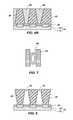
- a plurality of recesses 20are formed in a substrate structure 10 . While FIG. 1 shows four recesses 20 , the number of recesses 20 may be altered depending on the desired number of features to be formed.
- the substrate structure 10may include a substrate 12 and at least one other material, such as a hardmask 14 , supported by the substrate 12 .
- the term “substrate”means and includes a base material or construction upon which additional materials are formed.
- the substratemay be a semiconductor substrate, a base semiconductor layer on a supporting structure, a metal electrode, or a semiconductor substrate having one or more materials, structures, or regions formed thereon.
- the substratemay be a conventional silicon substrate or other bulk substrate including a semiconductive material.
- the term “bulk substrate”means and includes not only silicon wafers, but also silicon-on-insulator (SOI) substrates, such as silicon-on-sapphire (SOS) substrates and silicon-on-glass (SOG) substrates, epitaxial layers of silicon on a base semiconductor foundation, or other semiconductor or optoelectronic materials, such as silicon-germanium, germanium, gallium arsenide, gallium nitride, and indium phosphide.
- SOIsilicon-on-insulator
- SOSsilicon-on-sapphire
- SOGsilicon-on-glass
- the substratemay be doped or undoped. Furthermore, when reference is made to a “substrate” in the following description, previous process stages may have been utilized to form materials, regions, or junctions in or on the base semiconductor structure or foundation.
- the substrate 12is a semiconductor substrate.
- the hardmask 14may be at least one of a silicon- or a metal-containing material, a BARC, a TARC, an acid-rinsed material, and a topcoat material.
- the recesses 20may be formed at locations between which the openings are to be formed.
- the recesses 20may be periodic and formed at the same pitch as the contacts that are ultimately to be formed in the openings.
- the recesses 20may be formed in the hardmask 14 of the substrate structure 10 .
- the recesses 20may be shallow, e.g., extend partially into the thickness of the hardmask 14 .
- the recess 20may have a low aspect ratio (e.g., a ratio of the height of the recess 20 to the width of the recess 20 that is less than 1:1, e.g., 1:2 or 1:4).
- the height of the recesses 20may range from approximately 1 nm to approximately 250 nm, such as approximately 5 nm.
- the length of the recesses 20may range from approximately 1 ⁇ m to the length of the array.
- the width of the recesses 20may range from approximately 1 nm to approximately 40 nm, such as approximately 20 nm.
- the recesses 20may be formed by conventional methods, which are not described in detail herein.
- Pools 30 of acidic or basic materialmay be formed in the recesses 20 , as shown in FIG. 2 , by conventional methods, which are not described in detail herein.
- the locations of the pools 30may be determined by first determining where the features are to be formed.
- the pools 30may then be formed to be periodic and at the same pitch as the features that are ultimately to be formed in the openings.
- the pools 30may be supported by the substrate structure 10 .
- the pools 30 of acidic or basic materialmay include one of the materials previously described, such as the acidic pool material or the basic pool material. Selection of the material to be used as the pool material may depend on the material to be used as the resist and the development process to be used.
- the pool materialmay be dissolved in an organic solvent, and the solution of the pool material may be formed in the recesses 20 .
- the solution of the pool materialmay be spin-coated on the substrate structure 10 .
- the pool materialmay be exposed to heat (e.g., baked) to convert the pool material to a material immiscible in the organic solvent.
- the pools 30 and the hardmask 14may be planarized by an appropriate conventional method (e.g., chemical-mechanical planarization (CMP), a develop back process) so that an upper surface of the pools 30 is co-planar with a surface of the hardmask 14 .
- CMPchemical-mechanical planarization
- the pools 30may, alternatively, be subjected to a dry etch process to remove portions of the pool material.
- resist 40may be formed over the substrate structure 10 and the pools 30 .
- the resist 40may be formed after the pools 30 are made acidic or basic, or before the pools 30 are made acidic or basic. If, for example, the resist 40 is formed over the pools 30 before the pools 30 are made acidic or basic, the pools 30 may be heated (e.g., baked) after forming the resist 40 to generate the acid or the base.
- Forming the resist 40 over the pools 30may be accomplished using an appropriate conventional formation method, such as spin-coating of the material of the resist 40 .
- both the pool material and the resist 40are resist materials. Therefore, each of the pools 30 and the resist 40 may be formed using a solution of the pool material and a solution of the resist 40 , respectively.
- the organic solvent of the pool material and the resist 40may be selected depending on the miscibility and immiscibility of each other.
- the organic solventmay be an alcohol, cyclohexanone, propylene glycol methyl ether acetate (PGMEA), propylene glycol monomethyl ether (PGME), or combinations thereof.
- the resist 40may be formed over the pools 30 , the organic solvent in which the resist 40 is dissolved may be immiscible with the pool material. Accordingly, forming the resist 40 over the pools 30 may not affect the pools 30 .
- the pool materialmay be exposed to the energy source to convert the pool material to a material immiscible in the organic solvent, forming the pools 30 .
- the resist 40which may be the same resist material used as the pool material, may be formed over the pools 30 using the same organic solvent.
- the pools 30now being immiscible in the organic solvent, may not be affected by the formation of the resist 40 using the solution of the resist 40 in the organic solvent.
- the resist 40may be patterned to form openings 50 .
- an appropriate energy sourcee.g., light or radiation, or to a chemical composition
- the miscibility of exposed portions of the resist 40 in a developermay be altered relative to the miscibility of non-exposed portions of the resist 40 .
- a mask(not shown) may be used to selectively expose the resist 40 , forming exposed resist portions and non-exposed resist portions.
- the maskincludes a pattern that at least partially conforms to a pattern of openings 50 ultimately to be formed in the resist 40 .
- the acid or the base from the pools 30may diffuse into the resist 40 in the directions illustrated by arrows 60 in FIG. 4 .
- the acid or the basemay diffuse into portions of the resist 40 proximal to the pools 30 .
- the diffusion of the acid or the base from the pools 30may alter the acidity of the resist 40 , thus altering the miscibility of the resist 40 in the developer to be used during development.
- portions of the resist 40may be removed to form openings 50 in the resist 40 .
- a positive tone development process or a negative tone development processmay be used to remove the exposed or non-exposed resist portions.
- the desired portions of resist 40may be removed by appropriately selecting the developer in which the desired portions of resist 40 are miscible. Due to the respective acid or base diffusion, the resist 40 adjacent to (e.g., proximal to) the pools 30 may not be removed during development while the resist 40 distal to the substrate structure 10 and the pools 30 may be removed. Since portions of the resist 40 around the pools 30 remain, the proximal portions of the openings 50 in the resist 40 may have a narrower dimension than the distal portions.
- the openings 50 shown in FIG. 5Amay be formed by appropriately selecting the pool material, resist, positioning the mask, and using a positive tone developer or negative tone developer, as appropriate.
- a positive tone developermay be used to form the openings 50 .
- Base from each of the pools 30may diffuse into adjacent portions of the resist 40 , decreasing the acidity of the adjacent portions of the resist 40 relative to the other portions of resist 40 .
- the basemay neutralize acid in the adjacent portions of the resist 40 , decreasing the acid concentration in the adjacent portions of the resist 40 .
- the openings 50may be formed as shown in FIG. 5B .
- the openings 50are positioned directly over the pools 30
- FIG. 5Athe openings 50 are positioned between adjacent pools 30 (e.g., directly over exposed portions of the hardmask 14 ).
- a negative tone developermay be used to form the openings 50 .
- Base from the pools 30may diffuse into adjacent portions of the resist 40 , decreasing the acidity of the adjacent portions of the resist 40 relative to the other portions of resist 40 .
- the resist 40is subjected to an appropriately selected negative tone developer, the more basic portions of the resist 40 are soluble in the negative tone developer and are, thus, removed, forming the openings 50 .
- a negative tone developermay be used to form the openings 50 .
- Acid from the pools 30may diffuse into adjacent portions of the resist 40 , increasing the acidity of the adjacent portions of the resist 40 relative to the other portions of resist 40 .
- the acidmay increase the acid concentration in the adjacent portions of the resist 40 .
- the resist 40is subjected to the negative tone developer, the less acidic portions of the resist 40 are soluble in the negative tone developer and are, thus, removed, forming the openings 50 .
- a positive tone developermay be used to form the openings 50 .
- Acid from the pools 30may diffuse into adjacent portions of the resist 40 , increasing the acidity of the adjacent portions of the resist 40 relative to the other portions of resist 40 .
- the resist 40is subjected to the positive tone developer, the less acidic portions of the resist 40 are soluble in the positive tone developer and are, thus, removed, forming the openings 50 .
- Embodiments of the method of the present disclosuremay also be used to transfer the pattern (see FIGS. 5A and 5B ) in the resist 40 to the substrate structure 10 .
- the pattern in the resist 40may be transferred to the hardmask 14 and substrate 12 by an etch process.
- features (not shown) in the substrate structure 10may be formed that correspond to the pattern in the resist 40 .
- the features (not shown) in the substrate structure 10may be formed at a smaller size than is possible using conventional processes, such as at less than approximately 40 nm.
- the dimensions (e.g., width, length) of the openings 50 in the proximal portion of the resist 40may depend on the proximity to the pools 30 , the materials used as the pool material and resist 40 , and processing conditions used to form the openings 50 .
- concentration of the acid or the base in the pools 30By appropriately selecting the concentration of the acid or the base in the pools 30 , the size and location of the pools 30 , exposure conditions including the time and temperature of the exposure, and development conditions, the dimensions of the proximal portions of the openings 50 may be tailored as desired. For example, if the pools 30 are formulated to include a large concentration of the acid or the base, the dimensions of the proximal portions of the openings 50 may be narrower than if the pools 30 included a smaller concentration of the acid or the base.
- the dimensions of the proximal portions of the openings 50may be narrower than if the pools 30 were positioned a greater distance away. If large pools 30 are in close proximity to the openings 50 to be formed, the dimensions of the proximal portions of the openings 50 may be narrower than if the pools 30 were smaller. By increasing at least one of the amount of time and the temperature of exposure, the dimensions of the proximal portions of the openings 50 may be narrower than if a shorter amount of time and/or lower temperature are used.
- sidewalls of the resist 40 defining the openings 50may be sloped (e.g., non-vertical).
- the sidewalls of the openings 50would be substantially vertical, as shown in dashed lines on the left side of FIG. 5A , and the proximal portions and the distal portions of the openings 50 would have substantially the same diameter. While FIGS.
- 5A and 5Bshow the sidewalls of the resist 40 as having a uniform taper, the sidewalls may have a different profile (e.g., a non-uniform slope) depending on the proximity of the resist 40 to the pools 30 , the size of the pools 30 , and the concentration of the acid or the base in the pools 30 .
- a different profilee.g., a non-uniform slope
- the openings 50may be filled with a fill material, such as a conductive material, to form a semiconductor device structure 70 having features 80 .
- the fill materialmay be formed in the openings 50 by conventional techniques, which are not described in detail herein.
- the fill materialmay be a metal (e.g., tungsten, nickel, tantalum nitride (TaN), platinum, tungsten nitride (WN), gold, titanium nitride (TiN), or titanium aluminum nitride (TiAlN)), polysilicon, other conductive materials, or combinations thereof.
- the fill materialmay also be an oxide.
- the resist 40may subsequently be removed, such as by conventional techniques, with the features 80 remaining on the substrate structure 10 .
- the features 80may be positioned between adjacent pools 30 .
- FIG. 7which is a top down view of a feature 80 of FIG. 6A after the resist 40 has been removed, the feature 80 may have a tapered profile, with a proximal portion of the feature 80 having a narrower diameter than the distal portion.
- the features 80may overlay remaining portions of the hardmask 14 and be positioned between adjacent pools 30 .
- the pools 30may, optionally, be removed during subsequent processing acts to form memory devices including the features 80 .
- the openings 50 of FIG. 5Bmay be filled with the fill material to form a semiconductor device structure 70 having the features 80 positioned directly over the pools 30 , as shown in FIG. 6B .
- Disclosed is a method of forming a featurecomprising forming a resist over a pool of acidic or basic material on a substrate structure.
- the resistis selectively exposed to an energy source to form exposed resist portions and non-exposed resist portions.
- Acid or base of the acidic or basic materialis diffused from the pool into proximal portions of the resist.
- Also disclosed is a method of forming a featurecomprising forming a plurality of recesses in a substrate structure.
- the plurality of recessesare filled with a pool material comprising acid or base.
- a resistis formed over the pool material and the substrate structure and the acid or the base is diffused into adjacent portions of the resist.
- the resistis patterned to form openings in the resist.
- the openingscomprise wider portions distal to the substrate structure and narrower portions proximal to the substrate structure.
- the methodcomprises forming a plurality of recesses in a substrate structure.
- the plurality of recessesare filled with a pool material comprising acid or base and a resist is formed over the pool material and the substrate structure.
- the resistis selectively exposed to an energy source to form exposed resist portions and non-exposed resist portions.
- the acid or the baseis diffused from the pool material into adjacent portions of the resist to alter a solubility of the resist in a developer used to remove portions of the resist. Openings are formed in the resist, the openings comprising wider portions distal to the substrate structure and narrower portions proximal to the substrate structure.
- a semiconductor device structureis also disclosed.
- the semiconductor device structurecomprises a plurality of features on a substrate structure, each of the plurality of features comprising wider distal portions and narrower proximal portions.
- the narrower proximal portionsare adjacent a pool material comprising an acid or a base.
- the features 80may be formed at small sizes, such as at less than approximately 40 nm. In some embodiments, the features 80 are contacts having diameters of less than approximately 40 nm.
- the proximal portions of the openings 50may be narrower than the distal portions, enabling the features 80 formed in the openings 50 to self-align and contact underlying conductive traces (not shown).
- the features 80may be self-aligned and contact underlying the conductive traces. Accordingly, the features 80 may be formed with narrower dimensions at the portions proximal to the substrate structure 10 without using an etch process.
- the chemical proximity processmay also be used to form openings 50 overlying the pools 30 , as shown in FIG. 5B .
- the pools 30 in FIG. 5Bmay mark locations above which the openings 50 are to be formed.
- the openings 50(see FIG. 5B ) may be filled with the fill material to form a semiconductor device structure 70 having the features 80 positioned directly over the pools 30 , as shown in FIG. 6B .
- the chemical proximity processmay also be used to form features (not shown) in the substrate structure 10 by transferring the pattern in the resist 40 to the substrate structure 10 .
- the pattern in the resist 40(see FIGS. 5A and 5B ) may be transferred to the substrate structure 10 by a conventional etch process.
- the resulting features (not shown) in the substrate structure 10may be formed at smaller sizes than is possible using conventional processes due to the size of the openings 50 .
- the chemical proximity processmay also be used to form openings 50 having narrower distal portions and wider proximal portions, as shown in FIG. 8 .
- the openings 50 of FIG. 8may be formed substantially as described above in reference to FIGS. 1-5B .
- the chemical proximity processmay be used to form openings 50 having narrowed portions ( FIGS. 5A and 5B ) proximal to the substrate structure 10 in addition to openings 50 having widened portions ( FIG. 8 ) proximal to the substrate structure 10 .
- the openings 50 of FIG. 8may be filled with a fill material as described above.
- the pattern in the resist 40 of FIG. 8may be transferred to the substrate structure 10 as described above.
- the openings 50 or the resist 40may be self-aligned with the underlying pools 30 .
- the acid or the base from the pools 30may diffuse into the resist 40 during development.
- the acid or basemay diffuse into portions of the resist 40 adjacent to the pools 30 .
- the diffusion of the acid or the base from the pools 30may alter the acidity of the resist 40 , thus altering the miscibility of the resist 40 in the developer to be used during development.
- sidewalls of the openings 50 or the resist 40may be self-aligned with edges of the pools 30 .
- the methods described abovemay be used to form features 80 , such as contacts, for memory devices, such as, by way of non-limiting example, flash memory or dynamic random-access memory (DRAM) devices. However, the methods may also be used in other situations in which features having wider distal portions and narrower proximal portions are to be formed.
- the memory devicemay be used in wireless devices, personal computers, or other electronic devices.
Landscapes
- Engineering & Computer Science (AREA)
- Physics & Mathematics (AREA)
- Condensed Matter Physics & Semiconductors (AREA)
- General Physics & Mathematics (AREA)
- Computer Hardware Design (AREA)
- Microelectronics & Electronic Packaging (AREA)
- Power Engineering (AREA)
- Manufacturing & Machinery (AREA)
- Geometry (AREA)
- Photosensitive Polymer And Photoresist Processing (AREA)
Abstract
Description
Claims (20)
Priority Applications (2)
| Application Number | Priority Date | Filing Date | Title |
|---|---|---|---|
| US15/606,312US10032719B2 (en) | 2012-11-28 | 2017-05-26 | Semiconductor device structures |
| US16/042,255US10522461B2 (en) | 2012-11-28 | 2018-07-23 | Semiconductor device structures |
Applications Claiming Priority (5)
| Application Number | Priority Date | Filing Date | Title |
|---|---|---|---|
| US13/687,419US8815752B2 (en) | 2012-11-28 | 2012-11-28 | Methods of forming features in semiconductor device structures |
| US14/457,658US9142504B2 (en) | 2012-05-18 | 2014-08-12 | Semiconductor device structures |
| US14/848,912US9396996B2 (en) | 2012-05-18 | 2015-09-09 | Methods of forming openings in semiconductor structures |
| US15/192,060US9666531B2 (en) | 2012-05-18 | 2016-06-24 | Semiconductor device structures |
| US15/606,312US10032719B2 (en) | 2012-11-28 | 2017-05-26 | Semiconductor device structures |
Related Parent Applications (1)
| Application Number | Title | Priority Date | Filing Date |
|---|---|---|---|
| US15/192,060ContinuationUS9666531B2 (en) | 2012-05-18 | 2016-06-24 | Semiconductor device structures |
Related Child Applications (1)
| Application Number | Title | Priority Date | Filing Date |
|---|---|---|---|
| US16/042,255ContinuationUS10522461B2 (en) | 2012-11-28 | 2018-07-23 | Semiconductor device structures |
Publications (2)
| Publication Number | Publication Date |
|---|---|
| US20170263552A1 US20170263552A1 (en) | 2017-09-14 |
| US10032719B2true US10032719B2 (en) | 2018-07-24 |
Family
ID=50772526
Family Applications (6)
| Application Number | Title | Priority Date | Filing Date |
|---|---|---|---|
| US13/687,419ActiveUS8815752B2 (en) | 2012-05-18 | 2012-11-28 | Methods of forming features in semiconductor device structures |
| US14/457,658ActiveUS9142504B2 (en) | 2012-05-18 | 2014-08-12 | Semiconductor device structures |
| US14/848,912ActiveUS9396996B2 (en) | 2012-05-18 | 2015-09-09 | Methods of forming openings in semiconductor structures |
| US15/192,060ActiveUS9666531B2 (en) | 2012-05-18 | 2016-06-24 | Semiconductor device structures |
| US15/606,312ActiveUS10032719B2 (en) | 2012-11-28 | 2017-05-26 | Semiconductor device structures |
| US16/042,255ActiveUS10522461B2 (en) | 2012-11-28 | 2018-07-23 | Semiconductor device structures |
Family Applications Before (4)
| Application Number | Title | Priority Date | Filing Date |
|---|---|---|---|
| US13/687,419ActiveUS8815752B2 (en) | 2012-05-18 | 2012-11-28 | Methods of forming features in semiconductor device structures |
| US14/457,658ActiveUS9142504B2 (en) | 2012-05-18 | 2014-08-12 | Semiconductor device structures |
| US14/848,912ActiveUS9396996B2 (en) | 2012-05-18 | 2015-09-09 | Methods of forming openings in semiconductor structures |
| US15/192,060ActiveUS9666531B2 (en) | 2012-05-18 | 2016-06-24 | Semiconductor device structures |
Family Applications After (1)
| Application Number | Title | Priority Date | Filing Date |
|---|---|---|---|
| US16/042,255ActiveUS10522461B2 (en) | 2012-11-28 | 2018-07-23 | Semiconductor device structures |
Country Status (1)
| Country | Link |
|---|---|
| US (6) | US8815752B2 (en) |
Cited By (13)
| Publication number | Priority date | Publication date | Assignee | Title |
|---|---|---|---|---|
| WO2022180537A2 (en) | 2021-02-26 | 2022-09-01 | Cilag Gmbh International | Monitoring of manufacturing life-cycle |
| WO2022180540A2 (en) | 2021-02-26 | 2022-09-01 | Cilag Gmbh International | Adjustable communication based on available bandwidth and power capacity |
| WO2022180529A1 (en) | 2021-02-26 | 2022-09-01 | Cilag Gmbh International | Monitoring of multiple sensors over time to detect moving characteristics of tissue |
| WO2022180541A2 (en) | 2021-02-26 | 2022-09-01 | Cilag Gmbh International | Staple cartridge comprising an information access control system |
| WO2022180543A1 (en) | 2021-02-26 | 2022-09-01 | Cilag Gmbh International | Surgical instrument system comprising a power transfer coil |
| WO2022180520A1 (en) | 2021-02-26 | 2022-09-01 | Cilag Gmbh International | Stapling instrument comprising a signal antenna |
| WO2022180530A1 (en) | 2021-02-26 | 2022-09-01 | Cilag Gmbh International | Staple cartridge comprising a sensor array |
| WO2022180519A1 (en) | 2021-02-26 | 2022-09-01 | Cilag Gmbh International | Monitoring of internal systems to detect and track cartridge motion status |
| WO2022180525A2 (en) | 2021-02-26 | 2022-09-01 | Cilag Gmbh International | Staple cartridge comprising a sensing array and a temperature control system |
| WO2022180528A2 (en) | 2021-02-26 | 2022-09-01 | Cilag Gmbh International | Staple cartridge comprising a power management circuit |
| WO2022180533A1 (en) | 2021-02-26 | 2022-09-01 | Cilag Gmbh International | Stapling instrument comprising a separate power antenna and a data transfer antenna |
| WO2022180539A1 (en) | 2021-02-26 | 2022-09-01 | Cilag Gmbh International | Distal communication array to tune frequency of rf systems |
| WO2022180538A2 (en) | 2021-02-26 | 2022-09-01 | Cilag Gmbh International | Adjustment to transfer parameters to improve available power |
Families Citing this family (12)
| Publication number | Priority date | Publication date | Assignee | Title |
|---|---|---|---|---|
| US8815752B2 (en) | 2012-11-28 | 2014-08-26 | Micron Technology, Inc. | Methods of forming features in semiconductor device structures |
| US9291907B2 (en) | 2012-05-18 | 2016-03-22 | Micron Technology, Inc. | Methods for forming resist features and arrays of aligned, elongate resist features |
| US8999840B2 (en)* | 2013-07-11 | 2015-04-07 | Samsung Electronics Co., Ltd. | Method of forming fine patterns of semiconductor device |
| US9287124B2 (en)* | 2013-08-30 | 2016-03-15 | Applied Materials, Inc. | Method of etching a boron doped carbon hardmask |
| TWI517430B (en)* | 2013-12-31 | 2016-01-11 | 東旭能興業有限公司 | Solar battery unit and method of manufacturing same |
| US10115592B2 (en)* | 2016-12-15 | 2018-10-30 | Taiwan Semiconductor Manufacturing Co., Ltd. | Patterning process with silicon mask layer |
| US10991582B2 (en)* | 2016-12-21 | 2021-04-27 | Canon Kabushiki Kaisha | Template for imprint lithography including a recession, an apparatus of using the template, and a method of fabricating an article |
| KR102262024B1 (en) | 2017-04-03 | 2021-06-09 | 삼성전자주식회사 | Semiconductor devices |
| US10719517B1 (en)* | 2019-12-18 | 2020-07-21 | Snowflake Inc. | Distributed metadata-based cluster computing |
| CN117941028A (en)* | 2021-08-25 | 2024-04-26 | 杰米纳蒂奥公司 | Self-aligned stack construction method |
| US20240377749A1 (en)* | 2021-08-25 | 2024-11-14 | Geminatio, Inc. | Assisted feature placement in semiconductor patterning |
| WO2023076251A1 (en)* | 2021-10-26 | 2023-05-04 | Geminatio Inc. | Multi-level selective patterning for stacked device creation |
Citations (42)
| Publication number | Priority date | Publication date | Assignee | Title |
|---|---|---|---|---|
| US4599136A (en) | 1984-10-03 | 1986-07-08 | International Business Machines Corporation | Method for preparation of semiconductor structures and devices which utilize polymeric dielectric materials |
| US5877076A (en) | 1997-10-14 | 1999-03-02 | Industrial Technology Research Institute | Opposed two-layered photoresist process for dual damascene patterning |
| US6291118B1 (en) | 1998-03-27 | 2001-09-18 | Industrial Technology Research Institute | Elimination of proximity effect in photoresist |
| US20010045649A1 (en)* | 2000-05-25 | 2001-11-29 | Masato Sumikawa | Semiconductor device |
| US6613485B2 (en) | 1999-11-18 | 2003-09-02 | United Microelectronics Crop. | Optical proximity correction of pattern on photoresist through spacing of sub patterns |
| US20030165756A1 (en) | 2002-03-01 | 2003-09-04 | Yuko Ono | Developing method and developing unit |
| US6645702B1 (en) | 2000-05-01 | 2003-11-11 | Advanced Micro Devices, Inc. | Treat resist surface to prevent pattern collapse |
| US20040058550A1 (en) | 2002-09-19 | 2004-03-25 | Infineon Technologies North America Corp. | Dummy patterns for reducing proximity effects and method of using same |
| US6753115B2 (en) | 2001-12-20 | 2004-06-22 | Numerical Technologies, Inc. | Facilitating minimum spacing and/or width control optical proximity correction |
| US7033735B2 (en) | 2003-11-17 | 2006-04-25 | Taiwan Semiconductor Manufacturing Co., Ltd. | Water soluble negative tone photoresist |
| US7138654B2 (en) | 2003-12-26 | 2006-11-21 | Winbond Electronics Corp. | Chemical-mechanical polishing proximity correction method and correction pattern thereof |
| US20060263026A1 (en) | 2005-05-23 | 2006-11-23 | Imation Corp. | Optical waveguide disk |
| US20070105043A1 (en) | 2005-10-21 | 2007-05-10 | Klaus Elian | Photosensitive coating for enhancing a contrast of a photolithographic exposure |
| US20080076217A1 (en) | 2006-09-21 | 2008-03-27 | Henry Chien | Methods of Reducing Coupling Between Floating Gates in Nonvolatile Memory |
| US20080179715A1 (en)* | 2007-01-30 | 2008-07-31 | Micron Technology, Inc. | Shallow trench isolation using atomic layer deposition during fabrication of a semiconductor device |
| US20080179190A1 (en) | 2005-03-09 | 2008-07-31 | Phoenix Precision Technology Corporation | Method for fabrication of a conductive bump structure of a circuit board |
| US7429446B2 (en) | 2003-09-30 | 2008-09-30 | Fujitsu Limited | Resist pattern forming method and semiconductor device fabrication method |
| US7476612B2 (en) | 2005-11-30 | 2009-01-13 | Dongbu Hitek, Co., Ltd. | Method for manufacturing semiconductor device |
| US7485543B2 (en) | 2005-12-30 | 2009-02-03 | Hynix Semiconductor Inc. | Method for manufacturing semiconductor device with overlay vernier |
| US20090084310A1 (en) | 2007-09-28 | 2009-04-02 | Choi Si-Kyung | Method for manufacturing single crystal nano-structures capable of controlling morphology and device for manufacturing nano-structures |
| US20090214981A1 (en) | 2008-02-21 | 2009-08-27 | International Business Machines Corporation | Photoresists and methods for optical proximity correction |
| US20090214985A1 (en) | 2008-02-27 | 2009-08-27 | Tokyo Electron Limited | Method for reducing surface defects on patterned resist features |
| US20100130016A1 (en) | 2008-11-24 | 2010-05-27 | Micron Technology, Inc. | Methods of forming a masking pattern for integrated circuits |
| US20100164121A1 (en) | 2008-12-31 | 2010-07-01 | Frank Feustel | Metallization system of a semiconductor device comprising extra-tapered transition vias |
| US20100190346A1 (en) | 2003-05-09 | 2010-07-29 | Fujitsu Limited | Method of processing resist, semiconductor device, and method of producing the same |
| US7867844B2 (en) | 2008-05-28 | 2011-01-11 | Micron Technology, Inc. | Methods of forming NAND cell units |
| US7884014B2 (en) | 2007-07-10 | 2011-02-08 | Samsung Electronics Co., Ltd. | Method of forming contact structure with contact spacer and method of fabricating semiconductor device using the same |
| US20110068416A1 (en)* | 2009-09-21 | 2011-03-24 | Hynix Semiconductor Inc. | Semiconductor device and method for manufacturing the same |
| US20110084355A1 (en) | 2009-10-09 | 2011-04-14 | Taiwan Semiconductor Manufacturing Company, Ltd. | Isolation Structure For Semiconductor Device |
| US20110147984A1 (en) | 2009-12-18 | 2011-06-23 | Joy Cheng | Methods of directed self-assembly, and layered structures formed therefrom |
| US20110291224A1 (en) | 2006-09-14 | 2011-12-01 | Micron Technology, Inc. | Efficient pitch multiplication process |
| US8182982B2 (en) | 2008-04-19 | 2012-05-22 | Rolith Inc | Method and device for patterning a disk |
| US20120205805A1 (en)* | 2011-02-16 | 2012-08-16 | Chan Sun Hyun | Semiconductor device and method of manufacturing the same |
| US20130125988A1 (en) | 2009-11-25 | 2013-05-23 | E I Du Pont De Nemours And Company | CZTS/Se PRECURSOR INKS AND METHODS FOR PREPARING CZTS/Se THIN FILMS AND CZTS/Se-BASED PHOTOVOLTAIC CELLS |
| US20130189618A1 (en) | 2011-09-15 | 2013-07-25 | Tokyo Ohka Kogyo Co., Ltd | Method of forming resist pattern |
| US20130309605A1 (en) | 2012-05-18 | 2013-11-21 | Micron Technology, Inc. | Methods for forming resist features, patterns in a resist, and arrays of aligned, elongate resist features |
| US20140065818A1 (en) | 2012-08-30 | 2014-03-06 | Taiwan Semiconductor Manufacturing Company, Ltd. | Method of semiconductor integrated circuit fabrication |
| US20140061930A1 (en)* | 2012-09-06 | 2014-03-06 | International Business Machines Corporation | Overlay-tolerant via mask and reactive ion etch (rie) technique |
| US8673735B2 (en) | 2011-04-11 | 2014-03-18 | International Business Machines Corporation | Semiconductor device and method for making same |
| US20140145311A1 (en) | 2012-11-28 | 2014-05-29 | Micron Technology, Inc. | Methods of forming features in semiconductor device structures |
| US8748317B2 (en) | 2012-08-03 | 2014-06-10 | Infineon Technologies Austria Ag | Method of manufacturing a semiconductor device including a dielectric structure |
| US9125332B2 (en) | 2008-03-25 | 2015-09-01 | Stats Chippac, Ltd. | Filp chip interconnection structure with bump on partial pad and method thereof |
Family Cites Families (6)
| Publication number | Priority date | Publication date | Assignee | Title |
|---|---|---|---|---|
| CN101283388B (en)* | 2005-10-05 | 2011-04-13 | 出光兴产株式会社 | TFT substrate and method for manufacturing TFT substrate |
| US8119470B2 (en)* | 2007-03-21 | 2012-02-21 | Texas Instruments Incorporated | Mitigation of gate to contact capacitance in CMOS flow |
| KR100852207B1 (en)* | 2007-06-04 | 2008-08-13 | 삼성전자주식회사 | Removing insulating film and forming metal wiring |
| TWI344167B (en)* | 2007-07-17 | 2011-06-21 | Chunghwa Picture Tubes Ltd | Electron-emitting device and fabricating method thereof |
| WO2009115449A1 (en)* | 2008-03-19 | 2009-09-24 | Interuniversitair Microelektronica Centrum Vzw (Imec) | Method for fabricating through-substrate vias |
| US20140019716A1 (en)* | 2012-07-10 | 2014-01-16 | Christopher J. Jezewski | Plateable diffusion barrier techniques |
- 2012
- 2012-11-28USUS13/687,419patent/US8815752B2/enactiveActive
- 2014
- 2014-08-12USUS14/457,658patent/US9142504B2/enactiveActive
- 2015
- 2015-09-09USUS14/848,912patent/US9396996B2/enactiveActive
- 2016
- 2016-06-24USUS15/192,060patent/US9666531B2/enactiveActive
- 2017
- 2017-05-26USUS15/606,312patent/US10032719B2/enactiveActive
- 2018
- 2018-07-23USUS16/042,255patent/US10522461B2/enactiveActive
Patent Citations (47)
| Publication number | Priority date | Publication date | Assignee | Title |
|---|---|---|---|---|
| US4599136A (en) | 1984-10-03 | 1986-07-08 | International Business Machines Corporation | Method for preparation of semiconductor structures and devices which utilize polymeric dielectric materials |
| US5877076A (en) | 1997-10-14 | 1999-03-02 | Industrial Technology Research Institute | Opposed two-layered photoresist process for dual damascene patterning |
| US6291118B1 (en) | 1998-03-27 | 2001-09-18 | Industrial Technology Research Institute | Elimination of proximity effect in photoresist |
| US6613485B2 (en) | 1999-11-18 | 2003-09-02 | United Microelectronics Crop. | Optical proximity correction of pattern on photoresist through spacing of sub patterns |
| US6645702B1 (en) | 2000-05-01 | 2003-11-11 | Advanced Micro Devices, Inc. | Treat resist surface to prevent pattern collapse |
| US20010045649A1 (en)* | 2000-05-25 | 2001-11-29 | Masato Sumikawa | Semiconductor device |
| US6753115B2 (en) | 2001-12-20 | 2004-06-22 | Numerical Technologies, Inc. | Facilitating minimum spacing and/or width control optical proximity correction |
| US20030165756A1 (en) | 2002-03-01 | 2003-09-04 | Yuko Ono | Developing method and developing unit |
| US6955485B2 (en) | 2002-03-01 | 2005-10-18 | Tokyo Electron Limited | Developing method and developing unit |
| US20040058550A1 (en) | 2002-09-19 | 2004-03-25 | Infineon Technologies North America Corp. | Dummy patterns for reducing proximity effects and method of using same |
| US20100190346A1 (en) | 2003-05-09 | 2010-07-29 | Fujitsu Limited | Method of processing resist, semiconductor device, and method of producing the same |
| US7429446B2 (en) | 2003-09-30 | 2008-09-30 | Fujitsu Limited | Resist pattern forming method and semiconductor device fabrication method |
| US7033735B2 (en) | 2003-11-17 | 2006-04-25 | Taiwan Semiconductor Manufacturing Co., Ltd. | Water soluble negative tone photoresist |
| US7138654B2 (en) | 2003-12-26 | 2006-11-21 | Winbond Electronics Corp. | Chemical-mechanical polishing proximity correction method and correction pattern thereof |
| US20080179190A1 (en) | 2005-03-09 | 2008-07-31 | Phoenix Precision Technology Corporation | Method for fabrication of a conductive bump structure of a circuit board |
| US20060263026A1 (en) | 2005-05-23 | 2006-11-23 | Imation Corp. | Optical waveguide disk |
| US20070105043A1 (en) | 2005-10-21 | 2007-05-10 | Klaus Elian | Photosensitive coating for enhancing a contrast of a photolithographic exposure |
| US7476612B2 (en) | 2005-11-30 | 2009-01-13 | Dongbu Hitek, Co., Ltd. | Method for manufacturing semiconductor device |
| US7485543B2 (en) | 2005-12-30 | 2009-02-03 | Hynix Semiconductor Inc. | Method for manufacturing semiconductor device with overlay vernier |
| US20110291224A1 (en) | 2006-09-14 | 2011-12-01 | Micron Technology, Inc. | Efficient pitch multiplication process |
| US20080076217A1 (en) | 2006-09-21 | 2008-03-27 | Henry Chien | Methods of Reducing Coupling Between Floating Gates in Nonvolatile Memory |
| US20080179715A1 (en)* | 2007-01-30 | 2008-07-31 | Micron Technology, Inc. | Shallow trench isolation using atomic layer deposition during fabrication of a semiconductor device |
| US7884014B2 (en) | 2007-07-10 | 2011-02-08 | Samsung Electronics Co., Ltd. | Method of forming contact structure with contact spacer and method of fabricating semiconductor device using the same |
| US20090084310A1 (en) | 2007-09-28 | 2009-04-02 | Choi Si-Kyung | Method for manufacturing single crystal nano-structures capable of controlling morphology and device for manufacturing nano-structures |
| US20090214981A1 (en) | 2008-02-21 | 2009-08-27 | International Business Machines Corporation | Photoresists and methods for optical proximity correction |
| US20090214985A1 (en) | 2008-02-27 | 2009-08-27 | Tokyo Electron Limited | Method for reducing surface defects on patterned resist features |
| US9125332B2 (en) | 2008-03-25 | 2015-09-01 | Stats Chippac, Ltd. | Filp chip interconnection structure with bump on partial pad and method thereof |
| US8182982B2 (en) | 2008-04-19 | 2012-05-22 | Rolith Inc | Method and device for patterning a disk |
| US7867844B2 (en) | 2008-05-28 | 2011-01-11 | Micron Technology, Inc. | Methods of forming NAND cell units |
| US20100130016A1 (en) | 2008-11-24 | 2010-05-27 | Micron Technology, Inc. | Methods of forming a masking pattern for integrated circuits |
| US20100164121A1 (en) | 2008-12-31 | 2010-07-01 | Frank Feustel | Metallization system of a semiconductor device comprising extra-tapered transition vias |
| US20110068416A1 (en)* | 2009-09-21 | 2011-03-24 | Hynix Semiconductor Inc. | Semiconductor device and method for manufacturing the same |
| US20110084355A1 (en) | 2009-10-09 | 2011-04-14 | Taiwan Semiconductor Manufacturing Company, Ltd. | Isolation Structure For Semiconductor Device |
| US20130125988A1 (en) | 2009-11-25 | 2013-05-23 | E I Du Pont De Nemours And Company | CZTS/Se PRECURSOR INKS AND METHODS FOR PREPARING CZTS/Se THIN FILMS AND CZTS/Se-BASED PHOTOVOLTAIC CELLS |
| US20110147984A1 (en) | 2009-12-18 | 2011-06-23 | Joy Cheng | Methods of directed self-assembly, and layered structures formed therefrom |
| US20120205805A1 (en)* | 2011-02-16 | 2012-08-16 | Chan Sun Hyun | Semiconductor device and method of manufacturing the same |
| US8673735B2 (en) | 2011-04-11 | 2014-03-18 | International Business Machines Corporation | Semiconductor device and method for making same |
| US20130189618A1 (en) | 2011-09-15 | 2013-07-25 | Tokyo Ohka Kogyo Co., Ltd | Method of forming resist pattern |
| US20130309605A1 (en) | 2012-05-18 | 2013-11-21 | Micron Technology, Inc. | Methods for forming resist features, patterns in a resist, and arrays of aligned, elongate resist features |
| US20140353803A1 (en) | 2012-05-18 | 2014-12-04 | Micron Technology, Inc. | Semiconductor device structures |
| US20150380307A1 (en) | 2012-05-18 | 2015-12-31 | Micron Technology, Inc. | Methods of forming openings in semiconductor structures |
| US9291907B2 (en) | 2012-05-18 | 2016-03-22 | Micron Technology, Inc. | Methods for forming resist features and arrays of aligned, elongate resist features |
| US8748317B2 (en) | 2012-08-03 | 2014-06-10 | Infineon Technologies Austria Ag | Method of manufacturing a semiconductor device including a dielectric structure |
| US20140065818A1 (en) | 2012-08-30 | 2014-03-06 | Taiwan Semiconductor Manufacturing Company, Ltd. | Method of semiconductor integrated circuit fabrication |
| US20140061930A1 (en)* | 2012-09-06 | 2014-03-06 | International Business Machines Corporation | Overlay-tolerant via mask and reactive ion etch (rie) technique |
| US20140145311A1 (en) | 2012-11-28 | 2014-05-29 | Micron Technology, Inc. | Methods of forming features in semiconductor device structures |
| US8815752B2 (en) | 2012-11-28 | 2014-08-26 | Micron Technology, Inc. | Methods of forming features in semiconductor device structures |
Non-Patent Citations (3)
| Title |
|---|
| Berger, Cody M., "Measuring Acid Generation Kinetics in Photoresist Films Via Capacitance Techniques," Georgia Institute of Technology, available at https://smartech.gatech.edu/bitstream/handle/1853/7598/berger cody_m_200412phd.pdf, (Aug. 2004), 287 pages. |
| Prabhu et al., "Polyelectrolyte Effects in Model Photoresist Developer Solutions," J. Vac. Sci. Technol. B, vol. 21, No. 4, (Jul. 2003), pp. 1403-1410. |
| Shang et al., Verification of Numerical Simulation of the Self-Assembly of Polymer-Polymer-Solvent Ternary Blends on A Heterogeneously Functionalized Substrate, Polymer, vol. 52 (2011) pp. 1447-1457. |
Cited By (15)
| Publication number | Priority date | Publication date | Assignee | Title |
|---|---|---|---|---|
| WO2022180537A2 (en) | 2021-02-26 | 2022-09-01 | Cilag Gmbh International | Monitoring of manufacturing life-cycle |
| WO2022180540A2 (en) | 2021-02-26 | 2022-09-01 | Cilag Gmbh International | Adjustable communication based on available bandwidth and power capacity |
| WO2022180529A1 (en) | 2021-02-26 | 2022-09-01 | Cilag Gmbh International | Monitoring of multiple sensors over time to detect moving characteristics of tissue |
| WO2022180541A2 (en) | 2021-02-26 | 2022-09-01 | Cilag Gmbh International | Staple cartridge comprising an information access control system |
| WO2022180543A1 (en) | 2021-02-26 | 2022-09-01 | Cilag Gmbh International | Surgical instrument system comprising a power transfer coil |
| WO2022180520A1 (en) | 2021-02-26 | 2022-09-01 | Cilag Gmbh International | Stapling instrument comprising a signal antenna |
| WO2022180530A1 (en) | 2021-02-26 | 2022-09-01 | Cilag Gmbh International | Staple cartridge comprising a sensor array |
| WO2022180519A1 (en) | 2021-02-26 | 2022-09-01 | Cilag Gmbh International | Monitoring of internal systems to detect and track cartridge motion status |
| WO2022180525A2 (en) | 2021-02-26 | 2022-09-01 | Cilag Gmbh International | Staple cartridge comprising a sensing array and a temperature control system |
| WO2022180528A2 (en) | 2021-02-26 | 2022-09-01 | Cilag Gmbh International | Staple cartridge comprising a power management circuit |
| WO2022180533A1 (en) | 2021-02-26 | 2022-09-01 | Cilag Gmbh International | Stapling instrument comprising a separate power antenna and a data transfer antenna |
| WO2022180539A1 (en) | 2021-02-26 | 2022-09-01 | Cilag Gmbh International | Distal communication array to tune frequency of rf systems |
| WO2022180538A2 (en) | 2021-02-26 | 2022-09-01 | Cilag Gmbh International | Adjustment to transfer parameters to improve available power |
| EP4521595A2 (en) | 2021-02-26 | 2025-03-12 | Cilag GmbH International | Surgical instrument comprising means to measure a physical parameter |
| EP4524536A2 (en) | 2021-02-26 | 2025-03-19 | Cilag GmbH International | Staple cartridge comprising a sensing array and a temperature control system |
Also Published As
| Publication number | Publication date |
|---|---|
| US20160307839A1 (en) | 2016-10-20 |
| US9142504B2 (en) | 2015-09-22 |
| US20150380307A1 (en) | 2015-12-31 |
| US20170263552A1 (en) | 2017-09-14 |
| US9396996B2 (en) | 2016-07-19 |
| US20180366406A1 (en) | 2018-12-20 |
| US20140353803A1 (en) | 2014-12-04 |
| US10522461B2 (en) | 2019-12-31 |
| US20140145311A1 (en) | 2014-05-29 |
| US8815752B2 (en) | 2014-08-26 |
| US9666531B2 (en) | 2017-05-30 |
Similar Documents
| Publication | Publication Date | Title |
|---|---|---|
| US10522461B2 (en) | Semiconductor device structures | |
| US8492282B2 (en) | Methods of forming a masking pattern for integrated circuits | |
| US8389413B2 (en) | Method of manufacturing semiconductor device | |
| US7270917B2 (en) | Prevention of photoresist scumming | |
| US8435876B2 (en) | Method of manufacturing semiconductor device | |
| US10151981B2 (en) | Methods of forming structures supported by semiconductor substrates | |
| US8835324B2 (en) | Method for forming contact holes | |
| US9406526B2 (en) | Method for patterning contact openings on a substrate | |
| US20100099046A1 (en) | Method for manufacturing semiconductor device | |
| CN106252223A (en) | Semiconductor device and method for manufacturing the same | |
| US10734284B2 (en) | Method of self-aligned double patterning | |
| CN1996569B (en) | Method for manufacturing semiconductor device | |
| US8501619B1 (en) | Methods for forming a plurality of contact holes in a microelectronic device | |
| US9291907B2 (en) | Methods for forming resist features and arrays of aligned, elongate resist features | |
| US9798241B2 (en) | Methods of manufacturing photomasks, methods of forming photoresist patterns and methods of manufacturing semiconductor devices | |
| US10236185B2 (en) | Method of forming patterns for semiconductor device | |
| TW202314793A (en) | Method for removing material overburden via enhanced freeze-less anti-spacer formation using a bilayer system | |
| US6759351B2 (en) | Method for eliminating development related defects in photoresist masks | |
| US20150241780A1 (en) | Methods of forming insulation layer structures and methods of manufacturing metal interconnections | |
| US8268730B2 (en) | Methods of masking semiconductor device structures | |
| KR20110001718A (en) | Method for forming semiconductor device |
Legal Events
| Date | Code | Title | Description |
|---|---|---|---|
| AS | Assignment | Owner name:U.S. BANK NATIONAL ASSOCIATION, MINNESOTA Free format text:SUPPLEMENT NO. 5 TO PATENT SECURITY AGREEMENT;ASSIGNOR:MICRON TECHNOLOGY, INC.;REEL/FRAME:043483/0686 Effective date:20170721 Owner name:MORGAN STANLEY SENIOR FUNDING, INC., MARYLAND Free format text:SUPPLEMENT NO. 5 TO PATENT SECURITY AGREEMENT;ASSIGNOR:MICRON TECHNOLOGY, INC.;REEL/FRAME:043482/0776 Effective date:20170721 | |
| STCF | Information on status: patent grant | Free format text:PATENTED CASE | |
| AS | Assignment | Owner name:JPMORGAN CHASE BANK, N.A., AS COLLATERAL AGENT, ILLINOIS Free format text:SECURITY INTEREST;ASSIGNORS:MICRON TECHNOLOGY, INC.;MICRON SEMICONDUCTOR PRODUCTS, INC.;REEL/FRAME:047540/0001 Effective date:20180703 Owner name:JPMORGAN CHASE BANK, N.A., AS COLLATERAL AGENT, IL Free format text:SECURITY INTEREST;ASSIGNORS:MICRON TECHNOLOGY, INC.;MICRON SEMICONDUCTOR PRODUCTS, INC.;REEL/FRAME:047540/0001 Effective date:20180703 | |
| AS | Assignment | Owner name:MICRON TECHNOLOGY, INC., IDAHO Free format text:RELEASE BY SECURED PARTY;ASSIGNOR:U.S. BANK NATIONAL ASSOCIATION, AS AGENT;REEL/FRAME:046597/0393 Effective date:20180629 | |
| AS | Assignment | Owner name:MICRON TECHNOLOGY, INC., IDAHO Free format text:RELEASE BY SECURED PARTY;ASSIGNOR:MORGAN STANLEY SENIOR FUNDING, INC., AS COLLATERAL AGENT;REEL/FRAME:050700/0535 Effective date:20190731 | |
| AS | Assignment | Owner name:MICRON SEMICONDUCTOR PRODUCTS, INC., IDAHO Free format text:RELEASE BY SECURED PARTY;ASSIGNOR:JPMORGAN CHASE BANK, N.A., AS COLLATERAL AGENT;REEL/FRAME:051028/0001 Effective date:20190731 Owner name:MICRON TECHNOLOGY, INC., IDAHO Free format text:RELEASE BY SECURED PARTY;ASSIGNOR:JPMORGAN CHASE BANK, N.A., AS COLLATERAL AGENT;REEL/FRAME:051028/0001 Effective date:20190731 | |
| MAFP | Maintenance fee payment | Free format text:PAYMENT OF MAINTENANCE FEE, 4TH YEAR, LARGE ENTITY (ORIGINAL EVENT CODE: M1551); ENTITY STATUS OF PATENT OWNER: LARGE ENTITY Year of fee payment:4 |