US10019353B2 - Systems and methods for referencing data on a storage medium - Google Patents
Systems and methods for referencing data on a storage mediumDownload PDFInfo
- Publication number
- US10019353B2 US10019353B2US13/925,410US201313925410AUS10019353B2US 10019353 B2US10019353 B2US 10019353B2US 201313925410 AUS201313925410 AUS 201313925410AUS 10019353 B2US10019353 B2US 10019353B2
- Authority
- US
- United States
- Prior art keywords
- storage
- data
- solid
- index
- module
- Prior art date
- Legal status (The legal status is an assumption and is not a legal conclusion. Google has not performed a legal analysis and makes no representation as to the accuracy of the status listed.)
- Active, expires
Links
Images


Classifications
- G—PHYSICS
- G06—COMPUTING OR CALCULATING; COUNTING
- G06F—ELECTRIC DIGITAL DATA PROCESSING
- G06F12/00—Accessing, addressing or allocating within memory systems or architectures
- G06F12/02—Addressing or allocation; Relocation
- G06F12/0223—User address space allocation, e.g. contiguous or non contiguous base addressing
- G06F12/023—Free address space management
- G06F12/0238—Memory management in non-volatile memory, e.g. resistive RAM or ferroelectric memory
- G—PHYSICS
- G06—COMPUTING OR CALCULATING; COUNTING
- G06F—ELECTRIC DIGITAL DATA PROCESSING
- G06F11/00—Error detection; Error correction; Monitoring
- G06F11/07—Responding to the occurrence of a fault, e.g. fault tolerance
- G06F11/08—Error detection or correction by redundancy in data representation, e.g. by using checking codes
- G06F11/10—Adding special bits or symbols to the coded information, e.g. parity check, casting out 9's or 11's
- G06F11/1076—Parity data used in redundant arrays of independent storages, e.g. in RAID systems
- G06F11/108—Parity data distribution in semiconductor storages, e.g. in SSD
- G—PHYSICS
- G06—COMPUTING OR CALCULATING; COUNTING
- G06F—ELECTRIC DIGITAL DATA PROCESSING
- G06F12/00—Accessing, addressing or allocating within memory systems or architectures
- G06F12/02—Addressing or allocation; Relocation
- G06F12/0223—User address space allocation, e.g. contiguous or non contiguous base addressing
- G06F12/023—Free address space management
- G06F12/0238—Memory management in non-volatile memory, e.g. resistive RAM or ferroelectric memory
- G06F12/0246—Memory management in non-volatile memory, e.g. resistive RAM or ferroelectric memory in block erasable memory, e.g. flash memory
- G—PHYSICS
- G06—COMPUTING OR CALCULATING; COUNTING
- G06F—ELECTRIC DIGITAL DATA PROCESSING
- G06F3/00—Input arrangements for transferring data to be processed into a form capable of being handled by the computer; Output arrangements for transferring data from processing unit to output unit, e.g. interface arrangements
- G06F3/06—Digital input from, or digital output to, record carriers, e.g. RAID, emulated record carriers or networked record carriers
- G06F3/0601—Interfaces specially adapted for storage systems
- G06F3/0602—Interfaces specially adapted for storage systems specifically adapted to achieve a particular effect
- G06F3/0608—Saving storage space on storage systems
- G—PHYSICS
- G06—COMPUTING OR CALCULATING; COUNTING
- G06F—ELECTRIC DIGITAL DATA PROCESSING
- G06F3/00—Input arrangements for transferring data to be processed into a form capable of being handled by the computer; Output arrangements for transferring data from processing unit to output unit, e.g. interface arrangements
- G06F3/06—Digital input from, or digital output to, record carriers, e.g. RAID, emulated record carriers or networked record carriers
- G06F3/0601—Interfaces specially adapted for storage systems
- G06F3/0628—Interfaces specially adapted for storage systems making use of a particular technique
- G06F3/0638—Organizing or formatting or addressing of data
- G06F3/064—Management of blocks
- G—PHYSICS
- G06—COMPUTING OR CALCULATING; COUNTING
- G06F—ELECTRIC DIGITAL DATA PROCESSING
- G06F3/00—Input arrangements for transferring data to be processed into a form capable of being handled by the computer; Output arrangements for transferring data from processing unit to output unit, e.g. interface arrangements
- G06F3/06—Digital input from, or digital output to, record carriers, e.g. RAID, emulated record carriers or networked record carriers
- G06F3/0601—Interfaces specially adapted for storage systems
- G06F3/0668—Interfaces specially adapted for storage systems adopting a particular infrastructure
- G06F3/0671—In-line storage system
- G06F3/0673—Single storage device
- G06F3/0679—Non-volatile semiconductor memory device, e.g. flash memory, one time programmable memory [OTP]
- H—ELECTRICITY
- H04—ELECTRIC COMMUNICATION TECHNIQUE
- H04L—TRANSMISSION OF DIGITAL INFORMATION, e.g. TELEGRAPHIC COMMUNICATION
- H04L12/00—Data switching networks
- H04L12/28—Data switching networks characterised by path configuration, e.g. LAN [Local Area Networks] or WAN [Wide Area Networks]
- H04L12/46—Interconnection of networks
- H04L12/4604—LAN interconnection over a backbone network, e.g. Internet, Frame Relay
- H04L12/462—LAN interconnection over a bridge based backbone
- H04L12/4625—Single bridge functionality, e.g. connection of two networks over a single bridge
- H—ELECTRICITY
- H04—ELECTRIC COMMUNICATION TECHNIQUE
- H04L—TRANSMISSION OF DIGITAL INFORMATION, e.g. TELEGRAPHIC COMMUNICATION
- H04L12/00—Data switching networks
- H04L12/64—Hybrid switching systems
- H04L12/6418—Hybrid transport
- H—ELECTRICITY
- H04—ELECTRIC COMMUNICATION TECHNIQUE
- H04L—TRANSMISSION OF DIGITAL INFORMATION, e.g. TELEGRAPHIC COMMUNICATION
- H04L12/00—Data switching networks
- H04L12/66—Arrangements for connecting between networks having differing types of switching systems, e.g. gateways
- H—ELECTRICITY
- H05—ELECTRIC TECHNIQUES NOT OTHERWISE PROVIDED FOR
- H05K—PRINTED CIRCUITS; CASINGS OR CONSTRUCTIONAL DETAILS OF ELECTRIC APPARATUS; MANUFACTURE OF ASSEMBLAGES OF ELECTRICAL COMPONENTS
- H05K7/00—Constructional details common to different types of electric apparatus
- H05K7/14—Mounting supporting structure in casing or on frame or rack
- H05K7/1438—Back panels or connecting means therefor; Terminals; Coding means to avoid wrong insertion
- H05K7/1439—Back panel mother boards
- H05K7/1444—Complex or three-dimensional-arrangements; Stepped or dual mother boards
- G06F2003/0694—
- G—PHYSICS
- G06—COMPUTING OR CALCULATING; COUNTING
- G06F—ELECTRIC DIGITAL DATA PROCESSING
- G06F2211/00—Indexing scheme relating to details of data-processing equipment not covered by groups G06F3/00 - G06F13/00
- G06F2211/10—Indexing scheme relating to G06F11/10
- G06F2211/1002—Indexing scheme relating to G06F11/1076
- G06F2211/109—Sector level checksum or ECC, i.e. sector or stripe level checksum or ECC in addition to the RAID parity calculation
- G—PHYSICS
- G06—COMPUTING OR CALCULATING; COUNTING
- G06F—ELECTRIC DIGITAL DATA PROCESSING
- G06F2212/00—Indexing scheme relating to accessing, addressing or allocation within memory systems or architectures
- G06F2212/40—Specific encoding of data in memory or cache
- G06F2212/401—Compressed data
- G—PHYSICS
- G06—COMPUTING OR CALCULATING; COUNTING
- G06F—ELECTRIC DIGITAL DATA PROCESSING
- G06F2212/00—Indexing scheme relating to accessing, addressing or allocation within memory systems or architectures
- G06F2212/72—Details relating to flash memory management
- G06F2212/7201—Logical to physical mapping or translation of blocks or pages
- G—PHYSICS
- G06—COMPUTING OR CALCULATING; COUNTING
- G06F—ELECTRIC DIGITAL DATA PROCESSING
- G06F2212/00—Indexing scheme relating to accessing, addressing or allocation within memory systems or architectures
- G06F2212/72—Details relating to flash memory management
- G06F2212/7208—Multiple device management, e.g. distributing data over multiple flash devices
- G—PHYSICS
- G06—COMPUTING OR CALCULATING; COUNTING
- G06F—ELECTRIC DIGITAL DATA PROCESSING
- G06F3/00—Input arrangements for transferring data to be processed into a form capable of being handled by the computer; Output arrangements for transferring data from processing unit to output unit, e.g. interface arrangements
- G06F3/06—Digital input from, or digital output to, record carriers, e.g. RAID, emulated record carriers or networked record carriers
- G06F3/0601—Interfaces specially adapted for storage systems
- G06F3/0628—Interfaces specially adapted for storage systems making use of a particular technique
- G06F3/0662—Virtualisation aspects
- G06F3/0664—Virtualisation aspects at device level, e.g. emulation of a storage device or system
- H—ELECTRICITY
- H04—ELECTRIC COMMUNICATION TECHNIQUE
- H04L—TRANSMISSION OF DIGITAL INFORMATION, e.g. TELEGRAPHIC COMMUNICATION
- H04L67/00—Network arrangements or protocols for supporting network services or applications
- H04L67/01—Protocols
- H04L67/10—Protocols in which an application is distributed across nodes in the network
- H04L67/1097—Protocols in which an application is distributed across nodes in the network for distributed storage of data in networks, e.g. transport arrangements for network file system [NFS], storage area networks [SAN] or network attached storage [NAS]
Definitions
- This disclosurerelates to data storage and, in particular, to systems and methods for efficiently referencing data stored on a non-volatile storage medium.
- a storage systemmay map logical addresses to storage locations of a storage device.
- Physical addressing metadata used to reference the storage locationsmay consume significant memory resources.
- the size of the physical addressing metadatamay limit the size of the storage resources the system is capable of referencing.
- the methodmay comprise arranging a plurality of data segments for storage at respective offsets within a storage location of a solid-state storage medium, mapping front-end addresses of the data segments to an address of the storage location in a first index, and generating a second index configured for storage on the solid-state storage medium, wherein the second index is configured to associate the front-end addresses of the data segments with respective offsets of the data segments within the storage location.
- the methodfurther includes compressing one or more of the data segments for storage on the solid-state storage medium such that a compressed size of the compressed data segments differs from an uncompressed size of the data segments, wherein the offsets of the data segments within the storage location are based on the compressed size of the one or more data segments.
- the disclosed methodmay further comprise storing the second index on the storage medium.
- the second indexmay be stored on the storage location that comprises the plurality of data segments.
- the offsetsmay be omitted from the first index, which may reduce the overhead of the first index and/or allow the first index to reference a larger storage address space.
- the storage address of a data segment associated with a particular front-end addressmay be determined by use of a storage location address mapped to the particular front-end address in the first index and a data segment offset associated with the particular front-end address of the second index stored on the storage location.
- Accessing a requested data segment of a specified front-end addressmay include accessing a physical address of a storage location mapped to the specified front-end address in the first index, and reading the second index stored on the storage location to determine an offset of the requested data segment within the storage location.
- the apparatusmay include a storage layer configured to store data packets within storage units of a non-volatile storage medium, wherein the storage units are configured to store a plurality of data packets, a data layout module configured to determine relative locations of the stored data packets within the storage units, and an offset index module configured to generate offset indexes for the storage units based on the determined relative locations of the data packets stored within the storage units, wherein the offset index of a storage unit is configured to associate logical identifiers of data packets stored within the storage unit with the determined relative locations of the data packets within the storage unit.
- the disclosed apparatusfurther includes a compression module configured to compress data of one or more of the data packets, such that a compressed size of the data differs from an uncompressed size of the data, wherein the offset index module is configured to determine the offsets of the data packets based on the compressed size of the data.
- the apparatusmay further comprise a translation module which may be used to associate logical identifiers with media addresses of storage units comprising data packets corresponding to the logical identifiers, wherein the storage layer is configured to access a data packet corresponding to a logical identifier by use of a media address of a storage unit associated with the logical identifier by the translation module, and an offset index indicating a relative location of the data packet within the storage unit, wherein the offset index is stored at a pre-determined location within the storage unit.
- a translation modulewhich may be used to associate logical identifiers with media addresses of storage units comprising data packets corresponding to the logical identifiers
- the storage layeris configured to access a data packet corresponding to a logical identifier by use of a media address of a storage unit associated with the logical identifier by the translation module, and an offset index indicating a relative location of the data packet within the storage unit, wherein the offset index is stored at a pre-determined location within the storage unit.
- the storage layermay be configured to store the offset indexes of the storage units at pre-determined locations within the storage units.
- the storage layermay be further configured to store each offset index within the storage unit that comprises data packets indexed by the offset index.
- the storage mediummay comprise a solid-state storage array comprising a plurality of columns, each column comprising a respective solid-state storage element, and wherein each of the storage units comprises physical storage units on two or more columns of the solid-state storage array.
- the solid-state storage arraymay comprise a plurality of columns, each column comprising a respective solid-state storage element.
- the offset indexesmay indicate a relative location of a data packet within a column of the solid-state storage array.
- the storage mediumis a solid-state storage array comprising a plurality of independent channels, each channel comprising a plurality of solid-state storage elements, and wherein the offset indexes indicate relative locations of data packets within respective independent channels.
- the methodmay further comprise compressing the data for storage on the solid-state storage device, wherein the data offsets within respective storage units are based on a compressed size of the data.
- Data corresponding to a logical addressmay be accessed by combining a first portion of the physical address mapped to the logical address with a second portion of the physical address stored on a storage unit corresponding to the first portion of the physical address.
- each storage unitcomprises a plurality of storage units corresponding to respective solid-state storage elements.
- the storage unitmay comprise a page on a solid-state storage element, and the second portions of the physical addresses may correspond to a data offsets within the pages.
- FIG. 1Ais a block diagram of one embodiment of a computing system comprising a storage layer
- FIG. 1Bdepicts embodiments of any-to-any mappings
- FIG. 1Cdepicts one embodiment of a solid-state storage array
- FIG. 1Ddepicts one embodiment of a storage log
- FIG. 2is a block diagram of another embodiment of a storage layer
- FIG. 3depicts one embodiment of a packet format
- FIG. 4depicts one embodiment of ECC codewords comprising one or more data segments
- FIG. 5Ais a block diagram depicting one embodiment of a solid-state storage array
- FIG. 5Bis a block diagram depicting another embodiment of a solid-state storage array
- FIG. 5Cis a block diagram depicting another embodiment of banks of solid-state storage arrays
- FIG. 5Ddepicts one embodiment of sequential bank interleave
- FIG. 5Edepicts another embodiment of sequential bank interleave
- FIG. 6Ais a block diagram of another embodiment of a storage controller
- FIG. 6Bdepicts one embodiment of a horizontal data storage configuration
- FIG. 7Adepicts one embodiment of storage metadata for referencing data stored on a storage medium
- FIG. 7Bdepicts another embodiment of storage metadata for referencing data stored on a storage medium
- FIG. 7Cdepicts another embodiment of storage metadata for referencing data stored on a storage medium
- FIG. 8Adepicts one embodiment of a vertical data layout
- FIG. 8Bdepicts another embodiment of a vertical data layout
- FIG. 8Cdepicts one embodiment of a system for referencing data stored on a storage medium in a vertical data layout
- FIG. 9Ais a block diagram of one embodiment of a system for referencing data stored in an independent column layout on a storage medium
- FIG. 9Bis a block diagram of another embodiment of a system for referencing data stored in an independent column layout on a storage medium
- FIG. 9Cis a block diagram of another embodiment of a system for referencing data stored in an independent column layout on a storage medium
- FIG. 10Ais a block diagram of one embodiment of data stored in a vertical stripe configuration
- FIG. 10Bis a block diagram of one embodiment of a system for referencing data stored in a vertical stripe configuration
- FIG. 10Cis a block diagram of another embodiment of a system for referencing data stored in a vertical stripe configuration
- FIG. 10Dis a block diagram of another embodiment of a system for referencing data stored in a vertical stripe configuration
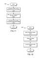
- FIG. 11is a flow diagram of one embodiment of a method for referencing data stored on a storage medium.
- FIG. 12is a flow diagram of another embodiment of a method for referencing data stored on a storage medium.
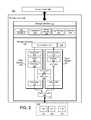
- FIG. 1Ais a block diagram of one embodiment of a computing system 100 comprising a storage layer 130 configured to provide storage services to one or more storage clients 106 .
- the computing system 100may comprise any suitable computing device, including, but not limited to: a server, desktop, laptop, embedded system, mobile device, and/or the like. In some embodiments, computing system 100 may include multiple computing devices, such as a cluster of server computing devices.
- the computing system 100may comprise processing resources 101 , volatile memory resources 102 (e.g., random access memory (RAM)), non-volatile storage resources 103 , and a communication interface 104 .
- the processing resources 101may include, but are not limited to, general purpose central processing units (CPUs), application-specific integrated circuits (ASICs), programmable logic elements, such as field programmable gate arrays (FPGAs), programmable logic arrays (PLGs), and the like.
- the non-volatile storage 103may comprise a non-transitory machine-readable storage medium, such as a magnetic hard disk, solid-state storage medium, optical storage medium, and/or the like.
- the communication interface 104may be configured to communicatively couple the computing system 100 to a network 105 .
- the network 105may comprise any suitable communication network including, but not limited to: a Transmission Control Protocol/Internet Protocol (TCP/IP) network, a Local Area Network (LAN), a Wide Area Network (WAN), a Virtual Private Network (VPN), a Storage Area Network (SAN), a Public Switched Telephone Network (PSTN), the Internet, and/or the like.
- TCP/IPTransmission Control Protocol/Internet Protocol
- LANLocal Area Network
- WANWide Area Network
- VPNVirtual Private Network
- SANStorage Area Network
- PSTNPublic Switched Telephone Network
- the computing system 100may comprise a storage layer 130 , which may be configured to provide storage services to one or more storage clients 106 .
- the storage clients 106may include, but are not limited to: operating systems (including bare metal operating systems, guest operating systems, virtual machines, virtualization environments, and the like), file systems, database systems, remote storage clients (e.g., storage clients communicatively coupled to the computing system 100 and/or storage layer 130 through the network 105 ), and/or the like.
- the storage layer 130may be implemented in software, hardware and/or a combination thereof.
- portions of the storage layer 130are embodied as executable instructions, such as computer program code, which may be stored on a persistent, non-transitory storage medium, such as the non-volatile storage resources 103 .
- the instructions and/or computer program codemay be configured for execution by the processing resources 101 .
- portions of the storage layer 130may be embodied as machine components, such as general and/or application-specific components, programmable hardware, FPGAs, ASICs, hardware controllers, storage controllers, and/or the like.
- the storage layer 130may be configured to perform storage operations on a storage medium 140 .
- the storage medium 140may comprise any storage medium capable of storing data persistently.
- “persistent” data storagerefers to storing information on a persistent, non-volatile storage medium.
- the storage medium 140may include non-volatile storage media such as solid-state storage media in one or more solid-state storage devices or drives (SSD), hard disk drives (e.g., Integrated Drive Electronics (IDE) drives, Small Computer System Interface (SCSI) drives, Serial Attached SCSI (SAS) drives, Serial AT Attachment (SATA) drives, etc.), tape drives, writable optical drives (e.g., CD drives, DVD drives, Blu-ray drives, etc.), and/or the like.
- SSDsolid-state storage media in one or more solid-state storage devices or drives
- IDEIntegrated Drive Electronics
- SCSISmall Computer System Interface
- SASSerial Attached SCSI
- SASSerial AT Attachment
- tape driveswritable
- the storage medium 140comprises non-volatile solid-state memory, which may include, but is not limited to, NAND flash memory, NOR flash memory, nano RAM (NRAM), magneto-resistive RAM (MRAM), phase change RAM (PRAM), Racetrack memory, Memristor memory, nanocrystal wire-based memory, silicon-oxide based sub-10 nanometer process memory, graphene memory, Silicon-Oxide-Nitride-Oxide-Silicon (SONOS), Resistive random-access memory (RRAM), programmable metallization cell (PMC), conductive-bridging RAM (CBRAM), and/or the like.
- NAND flash memoryNOR flash memory
- NRAMnano RAM
- MRAMmagneto-resistive RAM
- PRAMphase change RAM
- Racetrack memoryMemristor memory
- nanocrystal wire-based memorysilicon-oxide based sub-10 nanometer process memory
- graphene memorySilicon-Oxide-Nitride-Oxide-Silicon
- the teachings of this disclosurecould be applied to any suitable form of memory including both non-volatile and volatile forms. Accordingly, although particular embodiments of the storage layer 130 are disclosed in the context of non-volatile, solid-state storage devices 140 , the storage layer 130 may be used with other storage devices and/or storage media.
- the storage device 130includes volatile memory, which may include, but is not limited to RAM, dynamic RAM (DRAM), static RAM (SRAM), synchronous dynamic RAM (SDRAM), etc.
- the storage medium 140may correspond to memory of the processing resources 101 , such as a CPU cache (e.g., L1, L2, L3 cache, etc.), graphics memory, and/or the like.
- the storage medium 140is communicatively coupled to the storage layer 130 by use of an interconnect 127 .
- the interconnect 127may include, but is not limited to peripheral component interconnect (PCI), PCI express (PCI-e), serial advanced technology attachment (serial ATA or SATA), parallel ATA (PATA), small computer system interface (SCSI), IEEE 1394 (FireWire), Fiber Channel, universal serial bus (USB), and/or the like.
- the storage medium 140may be a remote storage device that is communicatively coupled to the storage layer 130 through the network 105 (and/or other communication interface, such as a Storage Area Network (SAN), a Virtual Storage Area Network (VSAN), or the like).
- SANStorage Area Network
- VSANVirtual Storage Area Network
- the interconnect 127may, therefore, comprise a remote bus, such as a PCE-e bus, a network connection (e.g., Infiniband), a storage network, Fibre Channel Protocol (FCP) network, HyperSCSI, and/or the like.
- a remote bussuch as a PCE-e bus, a network connection (e.g., Infiniband), a storage network, Fibre Channel Protocol (FCP) network, HyperSCSI, and/or the like.
- a network connectione.g., Infiniband
- FCPFibre Channel Protocol
- HyperSCSIHyperSCSI
- the storage layer 130may be configured to manage storage operations on the storage medium 140 by use of, inter alia, a storage controller 139 .
- the storage controller 139may comprise software and/or hardware components including, but not limited to: one or more drivers and/or other software modules operating on the computing system 100 , such as storage drivers, I/O drivers, filter drivers, and/or the like, hardware components, such as hardware controllers, communication interfaces, and/or the like, and so on.
- the storage medium 140may be embodied on a storage device 141 . Portions of the storage layer 139 (e.g., storage controller 139 ) may be implemented as hardware and/or software components (e.g., firmware) of the storage device 141 .
- the storage controller 139may be configured to implement storage operations at particular storage locations of the storage medium 140 .
- a storage locationrefers to unit of storage of a storage resource (e.g., a storage medium and/or device) that is capable of storing data persistently; storage locations may include, but are not limited to: pages, groups of pages (e.g., logical pages and/or offsets within a logical page), storage divisions (e.g., physical erase blocks, logical erase blocks, etc.), sectors, locations on a magnetic disk, battery-backed memory locations, and/or the like.
- the storage locationsmay be addressable within a storage address space 144 of the storage medium 140 .
- Storage addressesmay correspond to physical addresses, media addresses, back-end addresses, address offsets, and/or the like. Storage addresses may correspond to any suitable storage address space 144 , storage addressing scheme and/or arrangement of storage locations.
- the storage layer 130may comprise an interface 131 through which storage clients 106 may access storage services provided by the storage layer.
- the storage interface 131may include one or more of: a block device interface, a virtualized storage interface, an object storage interface, a database storage interface, and/or other suitable interface and/or Application Programming Interface (API).
- APIApplication Programming Interface
- the storage layer 130may provide for referencing storage resources through a front-end interface.
- a front-end interfacerefers to the identifiers used by the storage clients 106 to reference storage resources and/or services of the storage layer 130 .
- a front-end interfacemay correspond to a front-end address space 132 that comprises a set, range, and/or extent of front-end addresses or identifiers.
- a front-end addressrefers to an identifier used to reference data and/or storage resources; front-end addresses may include, but are not limited to: names (e.g., file names, distinguished names, etc.), data identifiers, logical identifiers (LIDs), logical addresses, logical block addresses (LBAs), logical unit number (LUN) addresses, virtual storage addresses, storage addresses, physical addresses, media addresses, and/or the like.
- the front-end address space 132comprises a logical address space, comprising a plurality of logical identifiers, LBAs, and/or the like.
- the translation module 134may be configured to map front-end identifiers of the front-end address space 132 to storage resources (e.g., data stored within the storage address space 144 of the storage medium 140 ).
- the front-end address space 132may be independent of the back-end storage resources (e.g., the storage medium 140 ); accordingly, there may be no set or pre-determined mappings between front-end addresses of the front-end address space 132 and the storage addresses of the storage address space 144 of the storage medium 140 .
- the front-end address space 132is sparse, thinly provisioned, and/or over-provisioned, such that the size of the front-end address space 132 differs from the storage address space 144 of the storage medium 140 .
- the storage layer 130may be configured to maintain storage metadata 135 pertaining to storage operations performed on the storage medium 140 .
- the storage metadata 135may include, but is not limited to: a forward index comprising any-to-any mappings between front-end identifiers of the front-end address space 132 and storage addresses within the storage address space 144 of the storage medium 140 , a reverse index pertaining to the contents of the storage locations of the storage medium 140 , one or more validity bitmaps, reliability testing and/or status metadata, status information (e.g., error rate, retirement status, and so on), and/or the like.
- Portions of the storage metadata 135may be maintained within the volatile memory resources 102 of the computing system 100 .
- portions of the storage metadata 135may be stored on non-volatile storage resources 103 and/or the storage medium 140 .
- FIG. 1Bdepicts one embodiment of any-to-any mappings 150 between front-end identifiers of the front-end address space 132 and back-end identifiers (e.g., storage addresses) within the storage address space 144 .
- the any-to-any mappings 150may be maintained in one or more data structures of the storage metadata 135 .
- the translation module 134may be configured to map any front-end address to any back-end storage location.
- the front-end address space 132may be sized differently than the underlying storage address space 144 .
- the front-end address space 132may be thinly provisioned, and, as such, may comprise a larger range of front-end identifiers than the range of storage addresses in the storage address space 144 .
- the storage layer 130may be configured to maintain the any-to-any mappings in a forward map 152 .
- the forward map 152may comprise any suitable data structure, including, but not limited to: an index, a map, a hash map, a hash table, an extended-range tree, a b-tree, and/or the like.
- the forward map 152may comprise entries 153 corresponding to front-end identifiers that have been allocated for use to reference data stored on the storage medium 140 .
- the entries 153 of the forward map 152may associate front-end identifiers 154 A-D with respective storage addresses 156 A-D within the storage address space 144 .
- the forward map 152may be sparsely populated, and as such, may omit entries corresponding to front-end identifiers that are not currently allocated by a storage client 106 and/or are not currently in use to reference valid data stored on the storage medium 140 .
- the forward map 152comprises a range-encoded data structure, such that one or more of the entries 153 may correspond to a plurality of front-end identifiers (e.g., a range, extent, and/or set of front-end identifiers).
- the forward map 152includes an entry 153 corresponding to a range of front-end identifiers 154 A mapped to a corresponding range of storage addresses 156 A.
- the entries 153may be indexed by front-end identifiers.
- the entries 153are arranged into a tree data structure by respective links.
- the disclosureis not limited in this regard, however, and could be adapted to use any suitable data structure and/or indexing mechanism.
- the solid-state storage medium 140may comprise a solid-state storage array 115 comprising a plurality of solid-state storage elements 116 A-Y.
- a solid-state storage array (or array) 115refers to a set of two or more independent columns 118 .
- a column 118may comprise one or more solid-state storage elements 116 A-Y that are communicatively coupled to the storage layer 130 in parallel using, inter alia, the interconnect 127 .
- Rows 117 of the array 115may comprise physical storage units of the respective columns 118 (solid-state storage elements 116 A-Y).
- a solid-state storage element 116 A-Yincludes, but is not limited to solid-state storage resources embodied as: a package, chip, die, plane, printed circuit board, and/or the like.
- the solid-state storage elements 116 A-Y comprising the array 115may be capable of independent operation. Accordingly, a first one of the solid-state storage elements 116 A may be capable of performing a first storage operation while a second solid-state storage element 116 B performs a different storage operation.
- the solid-state storage element 116 Amay be configured to read data at a first physical address, while another solid-state storage element 116 B reads data at a different physical address.
- a solid-state storage array 115may also be referred to as a logical storage element (LSE).
- the solid-state storage array 115may comprise logical storage units (rows 117 ).
- a “logical storage unit” or row 117refers to a logical construct combining two or more physical storage units, each physical storage unit on a respective column 118 of the array 115 .
- a logical erase blockrefers to a set of two or more physical erase blocks
- a logical pagerefers to a set of two or more pages, and so on.
- a logical erase blockmay comprise erase blocks within respective logical storage elements 115 and/or banks.
- a logical erase blockmay comprise erase blocks within a plurality of different arrays 115 and/or may span multiple banks of solid-state storage elements.
- the storage layer 130may further comprise a log storage module 136 configured to store data on the storage medium 140 in log structured storage configuration (e.g., in a storage log).
- a “storage log” or “log structure”refers to an ordered arrangement of data within the storage address space 144 of the storage medium 140 .
- the log storage module 136may be configured to append data sequentially within the storage address space 144 of the storage medium 140 .
- FIG. 1Ddepicts one embodiment of the storage address space 144 of the storage medium 140 .
- the storage address space 144comprises a plurality of storage divisions (e.g., erase blocks, logical erase blocks, or the like), each of which can be initialized (e.g., erased) for use in storing data.
- the storage divisions 160 A-Nmay comprise respective storage locations, which may correspond to pages, logical pages and/or the like.
- the storage locationsmay be assigned respective storage addresses (e.g., storage address 0 to storage address N).
- the log storage module 136may be configured to store data sequentially at an append point 180 within the physical address space 144 . Data may be appended at the append point 180 and, when the storage location 182 is filled, the append point 180 may advance 181 to a next available storage location.
- an “available” logical pagerefers to a logical page that has been initialized (e.g., erased) and has not yet been programmed. Some types of storage media can only be reliably programmed once after erasure. Accordingly, an available storage location may refer to a storage division 160 A-N that is in an initialized (or erased) state.
- Storage divisions 160 A-Nmay be reclaimed for use in a storage recovery process, which may comprise relocating valid data (if any) on the storage division 160 A-N that is being reclaimed to other storage division(s) 160 A-N and erasing the storage division 160 A-N.
- the logical erase block 160 Bmay be unavailable for storage due to, inter alia, not being in an erased state (e.g., comprising valid data), being out-of service due to high error rates or the like, and so on. Therefore, after filling the storage location 182 , the log storage module 136 may skip the unavailable storage division 160 B, and advance the append point 180 to the next available storage division 160 C.
- the log storage module 136may be configured to continue appending data to storage locations 183 - 185 , at which point the append point 180 continues at a next available storage division 160 A-N, as disclosed above.
- the append point 180After storing data on the “last” storage location within the storage address space 144 (e.g., storage location N 189 of storage division 160 N), the append point 180 wraps back to the first storage division 160 A (or the next available storage division, if storage division 160 A is unavailable). Accordingly, the log storage module 136 may treat the storage address space 144 as a loop or cycle.
- the storage layer 130may be configured to modify and/or overwrite data out-of-place.
- modifying and/or overwriting data “out-of-place”refers to performing storage operations at different storage addresses rather than modifying and/or overwriting the data at its current storage location (e.g., overwriting the original physical location of the data “in-place”).
- Performing storage operations out-of-placemay avoid write amplification, since existing, valid data on the storage division 160 A-N comprising the data that is being modified need not be erased and/or recopied.
- writing data “out-of-place”may remove erasure from the latency path of many storage operations (the erasure latency is no longer part of the “critical path” of a write operation). In the FIG.
- a storage operation to overwrite and/or modify data corresponding to front-end address A (denoted A 0 ) stored at physical storage location 191 with modified data A 1may be stored out-of-place on a different location (media address 193 ) within the storage address space 144 .
- Storing the data A 1may comprise updating the storage metadata 135 to associate the front end address A with the storage address of storage location 193 and/or to invalidate the obsolete data A 0 at storage address 191 .
- updating the storage metadata 135may comprise updating an entry of the forward map 152 to associate the front-end address A 154 E with the storage address of the modified data A 1 .
- the storage layer 130is configured to scan the storage address space 144 of the storage medium 140 to identify storage divisions 160 A-N to reclaim. As disclosed above, reclaiming a storage division 160 A-N may comprise relocating valid data on the storage division 160 A-N (if any) and erasing the storage division 160 A-N.
- the storage layer 130may be further configured to store data in association with persistent metadata (e.g., in a self-describing format).
- the persistent metadatamay comprise information about the data, such as the front-end identifier(s) associated with the data, data size, data length, and the like.
- Embodiments of a packet format comprising persistent, contextual metadata pertaining to data stored within the storage logare disclosed in further detail below in conjunction with FIG. 3 .
- the storage layer 130may be configured to reconstruct the storage metadata 135 by use of contents of the storage medium 140 .
- the current version of the data associated with front-end identifier A stored at storage location 191may be distinguished from the obsolete version of the data A stored at storage location 193 based on the log order of the packets at storage location 191 and 193 , respectively. Since the data packet at 193 is ordered after the data packet at 191 , the storage layer 130 may determine that storage location 193 comprises the most recent, up-to-date version of the data A. Accordingly, the reconstructed forward map 152 may associate front-end identifier A with the data stored at storage location 193 (rather than the obsolete data at storage location 191 ).
- FIG. 2is a block diagram of a system 200 comprising another embodiment of a storage layer 130 configured to manage data storage operations on a storage medium 140 .
- the storage medium 140may comprise one or more independent banks 119 A-N of solid-state storage arrays 115 A-N.
- Each of the solid-state storage arrays 115 A-Nmay comprise a plurality of solid-state storage elements (columns 118 ) communicatively coupled in parallel via the interconnect 127 , as disclosed herein.
- the storage controller 139may comprise a request module 231 configured to receive storage requests from the storage layer 130 and/or storage clients 106 .
- the request module 231may be configured to transfer data to/from the storage controller 139 in response to the requests.
- the request module 231may comprise and/or be communicatively coupled to one or more direct memory access (DMA) modules, remote DMA modules, interconnect controllers, bus controllers, bridges, buffers, network interfaces, and the like.
- DMAdirect memory access
- the storage controller 139may comprise a write module 240 configured to process data for storage on the storage medium 140 .
- the write module 240comprises one or more stages configured to process and/or format data for storage on the storage medium 140 , which may include, but are not limited to: a compression module 242 , a packet module 244 , an ECC write module 246 , and a write buffer 250 .
- the write module 240may further comprise a whitening module, configured to whiten data for storage on the storage medium 140 , one or more encryption modules configured to encrypt data for storage on the storage medium 140 , and so on.
- the read module 241may comprise one or more modules configured to process and/or format data read from the storage medium 140 , which may include, but are not limited to: a read buffer 251 , the data layout module 248 , an ECC read module 247 , a depacket module 245 , and a decompression module 243 .
- the write module 240comprises a write pipeline configured to process data for storage in a plurality of pipeline stages or modules, as disclosed herein.
- the read module 241may comprise a read pipeline configured to process data read from the solid-state storage array 115 in a plurality of pipeline stages or modules, as disclosed herein.
- the compression module 242may be configured to compress data for storage on the storage medium 140 .
- Datamay be compressed using any suitable compression algorithm and/or technique.
- the data compression module 242may be configured to compress the data, such that a compressed size of the data stored on the storage medium 140 differs from the original, uncompressed size of the data.
- the compression module 242may be configured to compress data using different compression algorithms and/or compression levels, which may result in variable compression ratios between the original, uncompressed size of certain data segments and the size of the compressed data segments.
- the compression module 242may be further configured to perform one or more whitening transformations on the data segments and/or data packets generated by the packet module 244 (disclosed in further detail below).
- the data whitening transformationsmay comprise decorrelating the data, which may provide wear-leveling benefits for certain types of storage media.
- the compression module 242may be further configured to encrypt data for storage on the storage medium 140 by use of one or more of a media encryption key, a user encryption key, and/or the like.
- the packet module 244may be configured to generate data packets comprising data to be stored on the storage medium 140 .
- the write module 240may be configured to store data in a storage log, in which data segments are stored in association with self-describing metadata in a packet format as illustrated in FIG. 3 .
- the packet module 244may be configured to generate packets comprising a data segment 312 and persistent metadata 314 .
- the persistent metadata 314may include one or more front-end addresses 315 associated with the data segment 312 .
- the data packets 310may be associated with sequence information, such as a sequence indicator 318 , to define, inter alia, a log-order of the data packets 310 within the storage log on the storage medium 140 .
- the sequence indicator 318may comprise one or more sequence numbers, timestamps, or other indicators from which a relative order of the data packets 310 stored on the storage medium 140 can be determined.
- the storage layer 130may use the data packets 310 stored within the storage log on the storage medium 140 to reconstruct portions of the storage metadata 135 , which may include, but is not limited to: reconstructing any-to-any mappings 150 between front-end addresses and storage addresses (e.g., the forward map 152 ), a reverse map, and/or the like.
- the packet module 244may be configured to generate packets of arbitrary lengths and/or sizes in accordance with the size of storage requests received via the request receiver module 231 , data compression performed by the compression module 242 , configuration, preferences, and so on.
- the packet module 244may be configured to generate packets of one or more pre-determined sizes.
- the packet module 244in response to a request to write 24k of data to the solid-state storage medium 110 , the packet module 244 may be configured to generate six packets, each packet comprising 4k of the data; in another embodiment, the packet module 244 may be configured to generate a single packet comprising 24k of data in response to the request.
- the persistent metadata 314may comprise the front-end identifier(s) 315 corresponding to the packet data segment 312 . Accordingly, the persistent metadata 314 may be configured to associate the packet data segment 312 with one or more LIDs, LBAs, and/or the like. The persistent metadata 314 may be used to associate the packet data segment 312 with the front-end identifier(s) independently of the storage metadata 135 . Accordingly, the storage layer 130 may be capable of reconstructing the storage metadata 135 (e.g., the forward map 152 ) by use of the storage log stored on the storage medium 140 .
- the persistent metadata 314may comprise other persistent metadata, which may include, but is not limited to, data attributes (e.g., an access control list), data segment delimiters, signatures, links, data layout metadata, and/or the like.
- the data packet 170may be associated with a log sequence indicator 318 .
- the log sequence indicator 318may be persisted on the storage division 160 A-N comprising the data packet 310 . Alternatively, the sequence indicator 318 may be persisted elsewhere on the storage medium 140 .
- the sequence indicator 178is applied to the storage divisions 160 A-N when the storage divisions 160 A-N are reclaimed (e.g., erased, when the first or last storage unit is programmed, etc.).
- the log sequence indicator 318may be used to determine the log-order of packets 310 within the storage log stored on the storage medium 140 (e.g., determine an ordered sequence of data packets 170 ).
- the ECC write module 246may be configured to encode data packets 310 generated by the packet module 244 into respective ECC codewords.
- an ECC codewordrefers to data and corresponding error detection and/or correction information.
- the ECC write module 246may be configured to implement any suitable ECC algorithm and may be configured to generate corresponding ECC information (e.g., ECC codewords), which may include, but are not limited to: data segments and corresponding ECC syndromes, ECC symbols, ECC chunks, and/or other structured and/or unstructured ECC information.
- ECC codewordsmay comprise any suitable error-correcting encoding, including, but not limited to: block ECC encoding, convolutional ECC encoding, Low-Density Parity-Check (LDPC) encoding, Gallager encoding, Reed-Solomon encoding, Hamming codes, Multidimensional parity encoding, cyclic error-correcting codes, BCH codes, and/or the like.
- the ECC write module 246may be configured to generate ECC codewords of a pre-determined size. Accordingly, a single packet may be encoded into a plurality of different ECC codewords and/or a single ECC codeword may comprise portions of two or more packets.
- the ECC write module 246is configured to generate ECC codewords, each of which may comprise a data of length N and a syndrome of length S.
- the ECC write module 246may be configured to encode data segments into 240-byte ECC codewords, each ECC codeword comprising 224 bytes of data and 16 bytes of ECC syndrome information.
- the ECC encodingmay be capable of correcting more bit errors than the manufacturer of the storage medium 140 requires.
- the ECC write module 246may be configured to encode data in a symbolic ECC encoding, such that each data segment of length N produces a symbol of length X.
- the ECC write module 246may encode data according to a selected ECC strength.
- the “strength” of an error-correcting coderefers to the number of errors that can be detected and/or corrected by use of the error correcting code.
- the strength of the ECC encoding implemented by the ECC write module 246may be adaptive and/or configurable. The strength of the ECC encoding may be selected according to the reliability and/or error rate of the storage medium 140 .
- the strength of the ECC encodingmay be independent of the partitioning and/or data layout on the storage medium 140 , which may allow the storage layer 130 to select a suitable ECC encoding strength based on the conditions of the storage medium 140 , user requirements, and the like, as opposed to static and/or pre-determined ECC settings imposed by the manufacturer of the storage medium 140 .
- FIG. 4depicts one embodiment of data flow 400 between the packet module 244 and an ECC write module 246 .
- the packet module 244may be configured to generate packets 310 A- 310 N in response to one or more requests to store data on the storage medium 140 .
- the packets 310 A-Nmay comprise respective packet data segments 312 A, 312 B, and 312 N.
- the packets 310 A-Nmay further comprise persistent metadata embodied in respective packet headers 314 A, 314 B, and 314 N.
- the packets 310 A-Nmay be processed by, inter alia, the ECC write module 246 to generate ECC codewords 420 A-Z.
- the ECC codewordscomprise ECC codewords 420 A- 420 Z, each of which may comprise a portion of one or more of the packets 310 A-N and a syndrome (not shown). In other embodiments, the ECC codewords may comprise ECC symbols or the like.
- the packets 310 A-Nmay vary in size in accordance with the size of the respective packet data segments 312 A-N and/or header information 314 A-N.
- the packet module 244may be configured to generate packets 310 A-N of a fixed, uniform size.
- the ECC write module 246may be configured to generate ECC codewords 420 A-N having a uniform, fixed size; each ECC codeword 420 A-N may comprise N bytes of packet data and S syndrome bytes, such that each ECC codeword 420 A-N comprises N+S bytes.
- each ECC codewordcomprises 240 bytes, and includes 224 bytes of packet data (N) and 16 byes of error correction code (S).
- Serror correction code
- the disclosed embodimentsare not limited in this regard, however, and could be adapted to generate ECC codewords 420 A-N of any suitable size, having any suitable ratio between N and S.
- the ECC write module 242may be further adapted to generate ECC symbols, or other ECC codewords, comprising any suitable ratio between data and ECC information.
- the ECC codewords 420 A-Nmay comprise portions of one or more packets 310 A-N; ECC codeword 420 D comprises data of packets 310 A and 310 B.
- the packets 310 A-Nmay be spread between a plurality of different ECC codewords 420 A-N: ECC codewords 420 A-D comprise data of packet 310 A; ECC codewords 420 D-H comprise data of packet 310 B; and ECC codewords 420 X-Z comprise data of packet 310 N.
- the write module 240may further comprise a data layout module 248 configured to buffer data for storage on one or more of the solid-state storage arrays 115 A-N.
- the data layout module 248may be configured to store data within one or more columns 118 of a solid-state storage array 115 .
- the data layout module 248may be further configured to generate parity data associated corresponding to the layout and/or arrangement of the data on the storage medium 140 .
- the parity datamay be configured to protect data stored within respective rows 117 of the solid-state storage array 115 A-N, and may be generated in accordance with the data layout implemented by the storage controller 139 .
- the write module 240further comprises a write buffer 250 configured to buffer data for storage within respective page write buffers of the storage medium 140 .
- the write buffer 250may comprise one or more synchronization buffers to synchronize a clock domain of the storage controller 139 with a clock domain of the storage medium 140 (and/or interconnect 127 ).
- the log storage module 136may be configured to select storage location(s) for data storage operations and/or may provide addressing and/or control information to the storage controller 139 . Accordingly, the log storage module 136 may provide for storing data sequentially at an append point 180 within the storage address space 144 of the storage medium 140 .
- the storage address at which a particular data segment is storedmay be independent of the front-end identifier(s) associated with the data segment.
- the translation module 134may be configured to associate the front-end interface of data segments (e.g., front-end identifiers of the data segments) with the storage address(es) of the data segments on the storage medium 140 .
- the translation module 134may leverage storage metadata 135 to perform logical-to-physical translations; the storage metadata 135 may include, but is not limited to: a forward map 152 comprising arbitrary, any-to-any mappings 150 between front-end identifiers and storage addresses; a reverse map comprising storage address validity indicators and/or any-to-any mappings between storage addresses and front-end identifiers; and so on.
- the storage metadata 135may be maintained in volatile memory, such as the volatile memory 102 of the computing system 100 .
- the storage layer 130is configured to periodically store portions of the storage metadata 135 on a persistent storage medium, such as the storage medium 140 , non-volatile storage resources 103 , and/or the like.
- the storage controller 139may further comprise a read module 241 that is configured to read data from the storage medium 140 in response to requests received via the request module 231 .
- the read module 241may be configured to process data read from the storage medium 140 , and provide the processed data to the storage layer 130 and/or a storage client 106 (by use of the request module 231 ).
- the read module 241may comprise one or more modules configured to process and/or format data read from the storage medium 140 , which may include, but is not limited to: read buffer 251 , data layout module 248 , ECC read module 247 , a depacket 245 , and a decompression module 243 .
- the read module 241further includes a dewhiten module configured to perform one or more dewhitening transforms on the data, a decryption module configured to decrypt encrypted data stored on the storage medium 140 , and so on.
- Data processed by the read module 241may flow to the storage layer 130 and/or directly to the storage client 106 via the request module 231 , and/or other interface or communication channel (e.g., the data may flow directly to/from a storage client via a DMA or remote DMA module of the storage layer 130 ).
- Read requestsmay comprise and/or reference the data using the front-end interface of the data, such as a front-end identifier (e.g., a logical identifier, an LBA, a range and/or extent of identifiers, and/or the like).
- the back-end addresses associated with data of the requestmay be determined based, inter alia, on the any-to-any mappings 150 maintained by the translation module 134 (e.g., forward map 152 ), metadata pertaining to the layout of the data on the storage medium 140 , and so on.
- Datamay stream into the read module 241 via a read buffer 251 .
- the read buffer 251may correspond to page read buffers of one or more of the solid-state storage arrays 115 A-N.
- the read buffer 251may comprise one or more synchronization buffers configured to synchronize a clock domain of the read buffer 251 with a clock domain of the storage medium 140 (and/or interconnect 127 ).
- the data layout module 248may be configured to reconstruct one or more data segments from the contents of the read buffer 251 .
- Reconstructing the data segmentsmay comprise recombining and/or reordering contents of the read buffer (e.g., ECC codewords) read from various columns 118 in accordance with a layout of the data on the solid-state storage arrays 115 A-N as indicated by the storage metadata 135 .
- reconstructing the datamay comprise stripping data associated with one or more columns 118 from the read buffer 251 , reordering data of one or more columns 118 , and so on.
- the read module 241may comprise an ECC read module 247 configured to detect and/or correct errors in data read from the solid-state storage medium 110 using, inter alia, the ECC encoding of the data (e.g., as encoded by the ECC write module 246 ), parity data (e.g., using parity substitution), and so on.
- the ECC encodingmay be capable of detecting and/or correcting a pre-determined number of bit errors, in accordance with the strength of the ECC encoding.
- the ECC read module 247may be capable of detecting more bit errors than can be corrected.
- the ECC read module 247may be configured to correct any “correctable” errors using the ECC encoding. In some embodiments, the ECC read module 247 may attempt to correct errors that cannot be corrected by use of the ECC encoding using other techniques, such as parity substitution, or the like. Alternatively, or in addition, the ECC read module 247 may attempt to recover data comprising uncorrectable errors from another source. For example, in some embodiments, data may be stored in a RAID configuration. In response to detecting an uncorrectable error, the ECC read module 247 may attempt to recover the data from the RAID, or other source of redundant data (e.g., a mirror, backup copy, or the like).
- redundant datae.g., a mirror, backup copy, or the like.
- the ECC read module 247may be configured to generate an interrupt in response to reading data comprising uncorrectable errors.
- the interruptmay comprise a message indicating that the requested data is in error, and may indicate that the ECC read module 247 cannot correct the error using the ECC encoding.
- the messagemay comprise the data that includes the error (e.g., the “corrupted data”).
- the interruptmay be caught by the storage layer 130 or other process, which, in response, may be configured to reconstruct the data using parity substitution, or other reconstruction technique, as disclosed herein.
- Parity substitutionmay comprise iteratively replacing portions of the corrupted data with a “parity mask” (e.g., all ones) until a parity calculation associated with the data is satisfied.
- the masked datamay comprise the uncorrectable errors, and may be reconstructed using other portions of the data in conjunction with the parity data.
- Parity substitutionmay further comprise reading one or more ECC codewords from the solid-state storage array 115 A-N (in accordance with an adaptive data structure layout on the array 115 ), correcting errors within the ECC codewords (e.g., decoding the ECC codewords), and reconstructing the data by use of the corrected ECC codewords and/or parity data.
- the corrupted datamay be reconstructed without first decoding and/or correcting errors within the ECC codewords.
- uncorrectable datamay be replaced with another copy of the data, such as a backup or mirror copy.
- the storage layer 130stores data in a RAID configuration, from which the corrupted data may be recovered.
- the solid-state storage medium 140may be arranged into a plurality of independent banks 119 A-N.
- Each bankmay comprise a plurality of solid-state storage elements arranged into respective solid-state storage arrays 115 A-N.
- the banks 119 A-Nmay be configured to operate independently; the storage controller 139 may configure a first bank 119 A to perform a first storage operation while a second bank 119 B is configured to perform a different storage operation.
- the storage controller 139may further comprise a bank controller 252 configured to selectively route data and/or commands to respective banks 119 A-N.
- storage controller 139is configured to read data from a bank 119 A while filling the write buffer 250 for storage on another bank 119 B and/or may interleave one or more storage operations between one or more banks 119 A-N.
- FIG. 2008/0229079U.S. patent application Ser. No. 11/952,095
- FIG. 6U.S. patent application Ser. No. 11/952,095
- the storage layer 130may further comprise a groomer module 138 configured to reclaim storage resources of the storage medium 140 .
- the groomer module 138may operate as an autonomous, background process, which may be suspended and/or deferred while other storage operations are in process.
- the log storage module 136 and groomer module 138may manage storage operations so that data is spread throughout the storage address space 144 of the storage medium 140 , which may improve performance and data reliability, and avoid overuse and underuse of any particular storage locations, thereby lengthening the useful life of the storage medium 140 (e.g., wear-leveling, etc.).
- datamay be sequentially appended to a storage log within the storage address space 144 at an append point 180 , which may correspond to a particular storage address within one or more of the banks 119 A-N (e.g., physical address 0 of bank 119 A).
- the append point 180may revert to the initial position (or next available storage location).
- operations to overwrite and/or modify data stored on the storage medium 140may be performed “out-of-place.”
- the obsolete version of overwritten and/or modified datamay remain on the storage medium 140 while the updated version of the data is appended at a different storage location (e.g., at the current append point 180 ).
- an operation to delete, erase, or TRIM data from the storage medium 140may comprise indicating that the data is invalid (e.g., does not need to be retained on the storage medium 140 ).
- Marking data as invalidmay comprise modifying a mapping between the front-end identifier(s) of the data and the storage address(es) comprising the invalid data, marking the storage address as invalid in a reverse map, and/or the like.
- the groomer module 138may be configured to select sections of the solid-state storage medium 140 for grooming operations.
- a “section” of the storage medium 140may include, but is not limited to: an erase block, a logical erase block, a die, a plane, one or more pages, a portion of a solid-state storage element 116 A-Y, a portion of a row 117 of a solid-state storage array 115 , a portion of a column 118 of a solid-state storage array 115 , and/or the like.
- a sectionmay be selected for grooming operations in response to various criteria, which may include, but are not limited to: age criteria (e.g., data refresh), error metrics, reliability metrics, wear metrics, resource availability criteria, an invalid data threshold, and/or the like.
- a grooming operationmay comprise relocating valid data on the selected section (if any).
- the operationmay further comprise preparing the section for reuse, which may comprise erasing the section, marking the section with a sequence indicator, such as the sequence indicator 318 , and/or placing the section into a queue of storage sections that are available to store data.
- the groomer module 138may be configured to schedule grooming operations with other storage operations and/or requests.
- the storage controller 139may comprise a groomer bypass (not shown) configured to relocate data from a storage section by transferring data read from the section from the read module 241 directly into the write module 240 without being routed out of the storage controller 139 .
- a groomer bypass(not shown) configured to relocate data from a storage section by transferring data read from the section from the read module 241 directly into the write module 240 without being routed out of the storage controller 139 .
- the storage layer 130may be further configured to manage out-of-service conditions on the storage medium 140 .
- a section of the storage medium 140 that is “out-of-service” (OOS)refers to a section that is not currently being used to store valid data.
- OOSout-of-service
- the storage layer 130may be configured to monitor storage operations performed on the storage medium 140 and/or actively scan the solid-state storage medium 140 to identify sections that should be taken out of service.
- the storage metadata 135may comprise OOS metadata that identifies OOS sections of the solid-state storage medium 140 .
- the storage layer 130may be configured to avoid OOS sections by, inter alia, streaming padding (and/or nonce) data to the write buffer 250 such that padding data will map to the identified OOS sections.
- the storage layer 130may be configured to manage OOS conditions by replacing OOS sections of the storage medium 140 with replacement sections.
- a hybrid OOS approachmay be used that combines adaptive padding and replacement techniques; the padding approach to managing OOS conditions may be used in portions of the storage medium 140 comprising a relatively small number of OOS sections; as the number of OOS sections increases, the storage layer 130 may replace one or more of the OOS sections with replacements sections.
- the storage medium 140may comprise one or more solid-state storage arrays 115 A-N.
- a solid-state storage array 115 A-Nmay comprise a plurality of independent columns 118 (respective solid-state storage elements 116 A-Y), which may be coupled to the storage layer 130 in parallel via the interconnect 127 . Accordingly, storage operations performed on an array 115 A-N may be performed on a plurality of solid-state storage elements 116 A-Y.
- Performing a storage operation on a solid-state storage array 115 A-Nmay comprise performing the storage operation on each of the plurality of solid-state storage elements 116 A-Y comprising the array 115 A-N: a read operation may comprise reading a physical storage unit (e.g., page) from a plurality of solid-state storage elements 116 A-Y; a program operation may comprise programming a physical storage unit (e.g., page) on a plurality of solid-state storage elements 116 A-Y; an erase operation may comprise erasing a section (e.g., erase block) on a plurality of solid-state storage elements 116 A-Y; and so on.
- a read operationmay comprise reading a physical storage unit (e.g., page) from a plurality of solid-state storage elements 116 A-Y
- a program operationmay comprise programming a physical storage unit (e.g., page) on a plurality of solid-state storage elements 116 A-Y
- an erase operationmay comprise eras
- a program operationmay comprise the write module 240 streaming data to program buffers of a plurality of solid-state storage elements 116 A-Y (via the write buffer 250 and interconnect 127 ) and, when the respective program buffers are sufficiently full, issuing a program command to the solid-state storage elements 116 A-Y.
- the program commandmay cause one or more storage units on each of the storage elements 116 A-Y to be programmed in parallel.
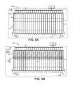
- FIG. 5Adepicts another embodiment 500 of a solid-state storage array 115 .
- the solid-state storage array 115may comprise a plurality of independent columns 118 , each of which may correspond to a respective set of one or more solid-state storage elements 116 A-Y.
- the solid-state storage array 115comprises 25 columns 118 (e.g., solid-state storage element 0 116 A through solid-state storage element 24 116 Y).
- the solid-state storage elements 116 A-Y comprising the arraymay be communicatively coupled to the storage layer 130 in parallel by the interconnect 127 .
- the interconnect 127may be capable of communicating data, addressing, and/or control information to each of the solid-state storage elements 116 A-Y.
- the parallel connectionmay allow the storage controller 139 to manage the solid-state storage elements 116 A-Y in parallel, as a single, logical storage element.
- the solid-state storage elements 116 A-Ymay be partitioned into sections, such as physical storage divisions 530 (e.g., physical erase blocks). Each erase block may comprise a plurality of physical storage units 532 , such as pages. The physical storage units 532 within a physical storage division 530 may be erased as a group.
- FIG. 5Adepicts a particular partitioning scheme, the disclosed embodiments are not limited in this regard, and could be adapted to use solid-state storage elements 116 A-Y partitioned in any suitable manner.
- the columns 118 of the array 115may correspond to respective solid-state storage elements 116 A-Y. Accordingly, the array 115 of FIG. 5A comprises 25 columns 118 . Rows of the array 117 may correspond to physical storage units 532 and/or 530 of a plurality of the columns 118 . In other embodiments, the columns 118 may comprise multiple solid-state storage elements.
- FIG. 5Bis a block diagram 501 of another embodiment of a solid-state storage array 115 .
- the solid-state storage array 115may comprise a plurality of rows 117 , which may correspond to storage units on a plurality of different columns 118 within the array 115 .
- the rows 117 of the solid-state storage array 115may include logical storage divisions 540 , which may comprise physical storage divisions on a plurality of the solid-state storage elements 116 A-Y.
- a logical storage division 540may comprise a logical erase block, comprising physical erase blocks of the solid-state storage elements 116 A-Y within the array 115 .
- a logical page 542may comprise physical storage units (e.g., pages) on a plurality of the solid-state storage elements 116 A-Y.
- Storage operations performed on the solid-state storage array 115may operate on multiple solid-state storage elements 116 A-Y: an operation to program data to a logical storage unit 542 may comprise programming data to each of 25 physical storage units (e.g., one storage unit per non-volatile storage element 116 A-Y); an operation to read data from a logical storage unit 542 may comprise reading data from 25 physical storage units (e.g., pages); an operation to erase a logical storage division 540 may comprise erasing 25 physical storage divisions (e.g., erase blocks); and so on. Since the columns 118 are independent, storage operations may be performed across different sets and/or portions of the array 115 .
- a read operation on the array 115may comprise reading data from physical storage unit 532 at a first physical address of solid-state storage element 116 A and reading data from a physical storage unit 532 at a different physical address of one or more other solid-state storage elements 116 B-N.
- Arranging solid-state storage elements 116 A-Y into a solid-state storage array 115may be used to address certain properties of the storage medium 140 .
- Some embodimentsmay comprise an asymmetric storage medium 140 , in which it takes longer to program data onto the solid-state storage elements 116 A-Y than it takes to read data therefrom (e.g., 10 times as long).
- datamay only be programmed to physical storage divisions 530 that have first been initialized (e.g., erased). Initialization operations may take longer than program operations (e.g., 10 times as long as a program, and by extension 100 times as long as a read operation).
- Managing groups of solid-state storage elements 116 A-Y in an array 115may allow the storage layer 130 to perform storage operations more efficiently, despite the asymmetric properties of the storage medium 140 .
- the asymmetry in read, program, and/or erase operationsis addressed by performing these operations on multiple solid-state storage elements 116 A-Y in parallel.
- programming asymmetrymay be addressed by programming 25 storage units in a logical storage unit 542 in parallel.
- Initialization operationsmay also be performed in parallel.
- Physical storage divisions 530 on each of the solid-state storage elements 116 A-Ymay be initialized as a group (e.g., as logical storage divisions 540 ), which may comprise erasing 25 physical erase blocks in parallel.
- portions of the solid-state storage array 115may be configured to store data and other portions of the array 115 may be configured to store error detection and/or recovery information.
- Columns 118 used for data storagemay be referred to as “data columns” and/or “data solid-state storage elements.”
- Columns used to store data error detection and/or recovery informationmay be referred to as a “parity column” and/or “recovery column.”
- the array 115may be configured in an operational mode in which one of the solid-state storage elements 116 Y is used to store parity data, whereas other solid-state storage elements 116 A-X are used to store data. Accordingly, the array 115 may comprise data solid-state storage elements 116 A-X and a recovery solid-state storage element 116 Y.
- the effective storage capacity of the rowsmay be reduced by one physical storage unit (e.g., reduced from 25 physical pages to 24 physical pages).
- the “effective storage capacity” of a storage unitrefers to the number of storage units or divisions that are available to store data and/or the total amount of data that can be stored on a logical storage unit.
- the operational mode described abovemay be referred to as a “24+1” configuration, denoting that twenty-four (24) physical storage units 532 are available to store data, and one (1) of the physical storage units 532 is used for parity.
- the disclosed embodimentsare not limited to any particular operational mode and/or configuration, and could be adapted to use any number of the solid-state storage elements 116 A-Y to store error detection and/or recovery data.
- FIG. 5Cis a block diagram of a system 502 comprising a storage controller 139 configured to manage storage divisions (logical erase blocks 540 ) that span multiple arrays 115 A-N of multiple banks 119 A-N.
- Each bank 119 A-Nmay comprise one or more solid-state storage arrays 115 A-N, which, as disclosed herein, may comprise a plurality of solid-state storage elements 116 A-Y coupled in parallel by a respective bus 127 A-N.
- the storage controller 139may be configured to perform storage operations on the storage elements 116 A-Y of the arrays 119 A-N in parallel and/or in response to a single command and/or signal.
- the storage controller 139may be configured to manage groups of logical erase blocks 540 that include erase blocks of multiple arrays 115 A-N within different respective banks 119 A-N. Each group of logical erase blocks 540 may comprise erase blocks 531 A-N on each of the arrays 115 A-N. The erase blocks 531 A-N comprising the logical erase block group 540 may be erased together (e.g., in response to a single erase command and/or signal or in response to a plurality of separate erase commands and/or signals). Performing erase operations on logical erase block groups 540 comprising large numbers of erase blocks 531 A-N within multiple arrays 115 A-N may further mask the asymmetric properties of the solid-state storage medium 140 , as disclosed herein.
- the storage controller 139may be configured to perform some storage operations within boundaries of the arrays 115 A-N and/or banks 119 A-N.
- the read, write, and/or program operationsmay be performed within rows 117 of the solid-state storage arrays 115 A-N (e.g., on logical pages 542 A-N within arrays 115 A-N of respective banks 119 A-N).
- the logical pages 542 A-N of the arrays 115 A-Nmay not extend beyond single arrays 115 A-N and/or banks 119 A-N.
- the log storage module 136 and/or bank interleave module 252may be configured to append data to the storage medium 140 by interleaving and/or scheduling storage operations sequentially between the arrays 115 A-N of the banks 119 A-N.
- FIG. 5Ddepicts one embodiment of storage operations that are interleaved between solid-state storage arrays 115 A-N of respective banks 119 A-N.
- the bank interleave module 252is configured to interleave programming operations between logical pages 542 A-N (rows 117 ) of the arrays 115 A-N within the banks 119 A-N.
- the write module 240may comprise a write buffer 250 , which may have sufficient capacity to fill write buffers one or more logical pages 542 A-N of an array 115 A-N.
- the storage controller 139may be configured to stream the contents of the write buffer 250 to program buffers of the solid-state storage elements 116 A-Y comprising one of the banks 119 A-N.
- the write module 240may then issue a program command and/or signal to the solid-state storage array 115 A-N to store the contents of the program buffers to a specified logical page 542 A-N.
- the log storage module 136 and/or bank interleave module 252may be configured to provide control and addressing information to the solid-state storage elements 116 A-Y of the array 115 A-N using a bus 127 A-N, as disclosed above.
- the bank interleave module 252may be configured to append data to the solid-state storage medium 110 by programming data to the arrays 115 A-N in accordance with a sequential interleave pattern.
- the sequential interleave patternmay comprise programming data to a first logical page (LP_ 0 ) of array 115 A within bank 119 A, followed by the first logical page (LP_ 0 ) of array 115 B within the next bank 119 B, and so on, until data is programmed to the first logical page LP_ 0 of each array 115 A-N within each of the banks 119 A-N. As depicted in FIG.
- datamay be programmed to the first logical page LP_ 0 of array 115 A in bank 119 A in a program operation 243 A.
- the bank interleave module 252may then stream data to the first logical page (LP_ 0 ) of the array 115 B in the next bank 119 B.
- the datamay then be programmed to LP_ 0 of array 115 B in bank 119 B in a program operation 243 B.
- the program operation 243 Bmay be performed concurrently with the program operation 243 A on array 115 A of bank 119 A; the data write module 240 may stream data to array 115 B and/or issue a command and/or signal for the program operation 243 B, while the program operation 243 A is being performed on the array 115 A.
- Datamay be streamed to and/or programmed on the first logical page (LP_ 0 ) of the arrays 115 C-N of the other banks 119 C- 119 N following the same sequential interleave pattern (e.g., after data is streamed and/or programmed to LP_ 0 of array 115 A of bank 119 B, data is streamed and/or programmed to LP_ 0 of array 115 C of bank 119 C in program operation 243 C, and so on).
- LP_ 0first logical page
- the bank interleave controller 252may be configured to begin streaming and/or programming data to the next logical page (LP_ 1 ) of array 115 A within the first bank 119 A, and the interleave pattern may continue accordingly (e.g., program LP_ 1 of array 115 B bank 119 B, followed by LP_ 1 of array 115 C bank 119 C through LP_ 1 of array 115 N bank 119 N, followed by LP_ 2 of array 115 A bank 119 A, and so on).
- program LP_ 1 of array 115 B bank 119 Bfollowed by LP_ 1 of array 115 C bank 119 C through LP_ 1 of array 115 N bank 119 N
- LP_ 2 of array 115 A bank 119 Aand so on.
- Sequentially interleaving programming operations as disclosed hereinmay increase the time between concurrent programming operations on the same array 115 A-N and/or bank 119 A-N, which may reduce the likelihood that the storage controller 139 will have to stall storage operations while waiting for a programming operation to complete.
- programming operationsmay take significantly longer than other operations, such as read and/or data streaming operations (e.g., operations to stream the contents of the write buffer 250 to an array 115 A-N via the bus 127 A-N).
- read and/or data streaming operationse.g., operations to stream the contents of the write buffer 250 to an array 115 A-N via the bus 127 A-N).
- 5Dmay be configured to avoid consecutive program operations on the same array 115 A-N and/or bank 119 A-N; programming operations on a particular array 115 A-N may be separated by N ⁇ 1 programming operations on other banks (e.g., programming operations on array 115 A are separated by programming operations on arrays 115 A-N). As such, programming operations on array 119 A are likely to be complete before another programming operation needs to be performed on the array 119 A.
- the interleave pattern for programming operationsmay comprise programming data sequentially across rows 117 (e.g., logical pages 542 A-N) of a plurality of arrays 115 A-N.
- the interleave patternmay result in interleaving programming operations between arrays 115 A-N of banks 119 A-N, such that the erase blocks of each array 115 A-N (erase block groups EBG_ 0 -N) are filled at the same rate.
- the sequential interleave patternprograms data to the logical pages of the first erase block group (EBG_ 0 ) in each array 115 A-N before programming data to logical pages LP_ 0 through LP_N of the next erase block group (EBG_ 1 ), and so on (e.g., wherein each erase block comprises 0-N pages).
- the interleave patterncontinues until the last erase block group EBG_N is filled, at which point the interleave pattern continues back at the first erase block group EBG_ 0 .
- the erase block groups of the arrays 115 A-Nmay, therefore, be managed as logical erase blocks 540 A-N that span the arrays 115 A-N.
- a logical erase block group 540may comprise erase blocks 531 A-N on each of the arrays 115 A-N within the banks 119 A-N.
- managing groups of erase blockse.g., logical erase block group 540
- erasing the logical erase block group 540 Amay comprise erasing EBG_ 0 of arrays 115 A-N in banks 119 A-N
- erasing a logical erase block group 540 Bmay comprise erasing EBG_ 1 of arrays 115 A-N in banks 517 A-N
- erasing logical erase block group 540 Cmay comprise erasing EBG_ 2 of arrays 115 A-N in banks 517 A-N
- erasing logical erase block group 540 Nmay comprise erasing EBG_N of arrays 115 A-N in banks 517 A-N.
- recovering the logical erase block group 540 Amay comprise relocating valid data (if any) stored on EBG_ 0 on arrays 115 A-N in banks 517 A-N, erasing the erase blocks of each EBG_ 0 in arrays A-N, and so on.
- each bank 119 A-Ncomprising a respective solid-state storage array 115 A-N comprising 25 storage elements 116 A-Y
- erasing, grooming, and/or recovering a logical erase block group 540comprises erasing, grooming, and/or recovering 100 physical erase blocks 530 .
- multi-bank embodimentsare described herein, the disclosure is not limited in this regard and could be configured using any multi-bank architecture comprising any number of banks 119 A-N of arrays 115 A-N comprising any number of solid-state storage elements 116 A-Y.
- the storage layer 130may be configured to store data segments in one or more different configurations, arrangements and/or layouts within a solid-state storage array 115 A-N (by use of the data layout module 248 ).
- the data layout module 248may be configured to buffer and/or arrange data in the write module 240 for storage in a particular arrangement within one or more of the solid-state storage arrays 115 A-N.
- the data layout module 248may configure data for “horizontal” storage within rows 117 of the array 115 (e.g., horizontally within logical storage units 542 of the array 115 ).
- a datastructuresuch as an ECC codeword, packet, or the like, may be spread across a plurality of the storage elements 116 A-Y comprising the logical storage unit 542 .
- datamay be stored horizontally within one or more independent “channels” of the array 115 .
- an independent channelor “channel” refers to a subset of one or more columns 118 of the array 115 (e.g., respective subsets of solid-state storage elements 116 A-Y).
- Datamay be arranged for storage within respective independent channels.
- An array 115 comprising N columns 118may be divided into a configurable number of independent channels X, each comprising Y columns 118 of the array 115 . In the FIG.
- the channel configurationsmay include, but are not limited to: 24 channels each comprising a single column 118 ; 12 channels each comprising two solid-state storage elements; eight channels each comprising three solid-state storage elements; six channels each comprising six columns 118 ; and so on.
- the array 115may be divided into heterogeneous channels, such as a first channel comprising 12 columns 118 and six other channels each comprising two columns 118 .
- the data layout module 248may be configured to arrange data for storage in a vertical code word configuration (disclosed in further detail below).
- FIG. 6Ais a block diagram of a system 600 comprising one embodiment of a storage controller 139 comprising a data layout module 248 configured to arrange data for storage on a solid-state storage array 115 in a horizontal configuration.
- the solid-state storage array 115comprises 25 solid-state storage elements 116 A-Y operating in a “24+1” configuration, in which 24 of the solid-state storage elements 116 A-X are used to store data, and one storage element ( 116 Y) is used to store parity data.
- the write module 240may comprise a packet module 244 configured to generate data packets comprising data segments for storage on the array 115 , as disclosed above.
- the packet module 244is configured to format data into a packet format 610 , comprising a packet data segment 612 and persistent metadata 614 (e.g., header).
- the header 614may comprise a front-end interface of the packet data segment 612 , a sequence number, and/or the like, as disclosed above.
- the packet module 244is configured to generate packets 610 of a fixed size (520-byte packet data segment 612 and 8 bytes of metadata 614 ).
- the ECC write module 246is configured to generate ECC datastructures (ECC codewords 620 ) comprising portions of one or more packets 610 , as disclosed above.
- the ECC codewords 620may be of a fixed size. In the FIG. 6A example, each ECC codeword 620 comprises 224 bytes of packet data and a 16-byte error-correcting code or syndrome. Although particular sizes and/or configurations of packets 610 and ECC codewords 620 are disclosed herein, the disclosure is not limited in this regard and could be adapted to use any size packets 610 and/or ECC codewords 620 .
- the size of the datastructuresmay vary.
- the size and/or contents of the packets 610 and/or ECC codewords 620may be adapted according to out-of-service conditions, as disclosed above.
- the data layout module 248may be configured to lay out data for horizontal storage within rows 117 of the array 115 .
- the data layout module 248may be configured to buffer and/or arrange data segments (e.g., the ECC codewords 621 , 622 , and 623 ) into data rows 667 comprising 24 bytes of data.
- the data layout module 248may be capable of buffering one or more ECC codewords 620 (by use of the write buffer 251 ). In the FIG. 6A embodiment, data layout module 248 may be configured to buffer 10 24-byte data rows, which is sufficient to buffer a full 240-byte ECC codeword 620 .
- the data layout module 248may be configured to lay out data segments for horizontal storage within rows 117 of the array 115 .
- the data layout module 248may be configured to buffer and/or arrange data segments (e.g., the ECC codewords 621 , 622 , and 623 ) into data rows 667 comprising 24 bytes of data.
- the data layout module 248may be capable of buffering one or more ECC codewords 620 (by use of the write buffer 251 ). In the FIG. 6A embodiment, data layout module 248 may be configured to buffer 10 24-byte data rows, which is sufficient to buffer a full 240-byte ECC codeword 620 .
- the data layout module 248may be further configured to stream 24-byte data rows to a parity module 637 , which may be configured to generate a parity byte for each 24-byte group.
- the data layout module 248streams the resulting 25-byte data rows 667 to the array 115 via the bank controller 252 and interconnect 127 (and/or write buffer 250 , as disclosed above).
- the storage controller 139may be configured to stream the data rows 667 to respective program buffers of the solid-state storage array 115 (e.g., stream to program buffers of respective solid-state storage elements 116 A-Y). Accordingly, each cycle of the interconnect 127 may comprise transferring a byte of a data row 667 to a program buffer of a respective solid-state storage element 116 A-Y.
- the solid-state storage elements 116 A-Xreceive data bytes of a data row 667 and solid-state storage element 116 Y receives the parity byte of the data row 667 .
- data of the ECC codewords 620may be byte-wise interleaved between the solid-state storage elements 116 A-X of the array 115 ; each solid-state storage element 116 A-X receives 10 bytes of each 240 byte ECC codeword 620 .
- a data row 667refers to a data set comprising data for each of a plurality of columns 118 within the array 115 .
- the data row 667may comprise a byte of data for each column 0 - 23 .
- the data row 667may further comprise a parity byte corresponding to the data bytes (e.g., a parity byte corresponding to the data bytes for columns 0 - 23 ).
- Data rows 667may be streamed to respective program buffers of the solid-state storage elements 116 A-Y via the interconnect 127 .
- streaming a 240-byte ECC codeword 620 to the array 115may comprise streaming 10 separate data rows 667 to the array 115 , each data row comprising 24 data bytes (one for each data solid-state storage element 116 A-X) and a corresponding parity byte.
- the storage locations of the solid-state storage array 115may be capable of storing a large number of ECC codewords 610 and/or packets 610 .
- the solid-state storage elementsmay comprise 8 kb pages, such that the storage capacity of a storage location (row 117 ) is 192 kb.
- each storage location within the array 115may be capable of storing approximately 819 240B ECC codewords (352 packets 610 ).
- the storage address of a data segmentmay, therefore, comprise: a) the address of the storage location on which the ECC codewords 620 and/or packets 610 comprising the data segment are stored, and b) an offset of the ECC codewords 620 and/or packets 610 within the row 117 .
- the storage location or offset 636 of the packet 610 A within the logical page 542 Amay be determined based on the horizontal layout of the data packet 610 A.
- the offset 636may identify the location of the ECC codewords 621 , 622 , and/or 623 comprising the packet 610 A (and/or may identify the location of the last ECC codeword 623 comprising data of the packet 610 A). Accordingly, in some embodiments, the offset may be relative to one or more datastructures on the solid-state storage array 115 (e.g., a packet offset and/or ECC codeword offset).
- Another offset 638may identify the location of the last ECC codeword of a next packet 620 (e.g., packet 610 B), and so on.
- each of the ECC codewords 621 , 622 , and 623are horizontally spread across the storage elements 116 A-Y comprising the logical page 542 A (e.g., 10 bytes of the ECC codewords 621 , 622 , and 623 are stored on each solid-state storage element 116 A-X). Accessing the packet 610 A may, therefore, comprise accessing each of the ECC codewords 621 , 622 , and 623 (and each of the storage elements 116 A-X).
- FIG. 6Bis a block diagram of a system 601 depicting one embodiment of a storage controller 139 configured to store data in a horizontal storage configuration.
- the FIG. 6B embodimentdepicts a horizontal layout of an ECC codeword 621 on the array 115 of FIG. 6A .
- Data D 0denotes a first byte of the ECC codeword 621
- data D 239denotes the last byte (byte 240 ) of the ECC codeword 621 .
- FIG. 6Bdepicts a block diagram of a system 601 depicting one embodiment of a storage controller 139 configured to store data in a horizontal storage configuration.
- the FIG. 6B embodimentdepicts a horizontal layout of an ECC codeword 621 on the array 115 of FIG. 6A .
- Data D 0denotes a first byte of the ECC codeword 621
- data D 239denotes the last byte (byte 240 ) of the ECC codeword 621 .
- each column 118 of the solid-state storage array 115comprises 10 bytes of the ECC codeword 621 , and the data of the ECC codeword 621 is horizontally spread across a row 117 of the array 115 (e.g., horizontally spread across solid-state storage elements 116 A-X of the array 115 ).
- FIG. 6Balso depicts a data row 667 as streamed to (and stored on) the solid-state storage array 115 . As illustrated in FIG. 6B , the data row 667 comprises bytes 0 through 23 of the ECC codeword D, each stored on a respective one of the columns 118 .
- the data row 667further comprises a parity byte 668 corresponding to the contents of the data row 667 (bytes D 0 through D 23 ).
- reading data of the ECC codeword 621may require accessing a plurality of columns 118 .
- the smallest read unitmay be an ECC codeword 620 (and/or packet 610 ).
- reading a data segmentmay comprise determining the storage address of the data by use of, inter alia, the translation module 134 (e.g., the forward map 152 ).
- the storage addressmay comprise a) the address of the storage location (logical page) on which the ECC codewords and/or packets comprising the requested data are stored, and b) the offset of the ECC codewords and/or packets within the particular storage location.
- the translation module 134may be configured to maintain a forward map 152 configured to index front-end identifiers to storage addresses on the storage medium 140 .
- the storage address of datamay comprise a) the address of the storage location (logical page) comprising the data and b) an offset of the data within the storage location.
- the storage addresses 156 A-D of the entries 153 within forward map 152may be segmented into a first portion comprising an address of a storage location and a second portion comprising the offset of the data within the storage location.
- Portions of the storage metadata 135may be stored in volatile memory of the computing system 100 and/or storage layer 130 .
- the memory footprint of the storage metadata 135may grow in proportion to the number of entries 153 that are included in the forward map 152 , as well as the size of the entries 153 themselves.
- the memory footprint of the forward map 152may be related the size (e.g., number of bits) used to represent the storage address of each entry 153 .
- the memory footprint of the forward map 153may impact the performance of the computing system 100 hosting the storage layer 130 .
- the computing device 100may exhaust its volatile memory resources 102 , and be forced to page swap memory to non-volatile storage resources 103 , or the like. Even small reductions in the size of the entries 153 may have a significant impact on the overall memory footprint of the storage metadata 135 when scaled to a large number of entries 153 .
- the number of the storage addresses 154 A-Dmay also determine the storage capacity that the forward map 152 is capable of referencing (e.g., may determine the number of unique storage locations that can be referenced by the entries 153 of the forward map 152 ).
- the entries 153may comprise 32 bit storage addresses 154 A-D. As disclosed above, a portion of each 32 bit storage addresses 154 A-D may be used to address a specific storage location (e.g., logical page), and other portions of the storage addresses 154 A-D may determine the offset within the storage location. If 4 bits are needed to represent storage location offsets, the 32 bit storage addresses 154 A-D may only be capable of addressing 2 ⁇ 28 unique storage locations.
- the storage layer 130comprises an offset index module 249 configured to determine the offsets of data segments within storage locations of the storage medium 140 .
- the offset index module 249may be further configured to generate an offset index configured to map front-end identifiers of the data segments to respective offsets within the storage locations.
- the offset indexmay be configured for storage on the storage medium 140 .
- the offset index module 249may, therefore, segment storage addresses into a first portion configured to address a storage location (logical page) on the storage medium 140 , and a second portion corresponding to an offset within the storage location.
- the storage controller 139may be configured to store the offset index (the second portion of the storage addresses) on the storage medium 140 .
- the translation module 134may be configured to index front-end addresses of the data using the first portion of the storage addresses.
- the second portion of the storage addressesmay be omitted from the forward map 152 , which may reduce the memory overhead of the forward map 152 and/or enable the forward map 152 to reference a larger storage address space 144 .
- FIG. 7Adepicts one embodiment of a system 700 for referencing data on a storage medium.
- the system 700comprises a forward map 152 that includes an entry 153 configured to associate a front-end address 754 D with a storage address 756 .
- Other entries 153 of the forward map 152are omitted from FIG. 7A to avoid obscuring the details of the depicted embodiments.
- the offset index module 249may segment the storage address into a first portion 757 and a second portion 759 D.
- the first portion 757may correspond to an address of a storage location and the second portion 759 D may identify an offset of the data segment within the storage location (e.g., within a logical page 542 ).
- the relative size of the offset portion 759 D of the storage address 756 to the storage location portion 757may be based on the size of the data packets 610 A-N stored on the solid-state storage array 115 , the size of the logical page 542 , and/or the layout of the packets 610 A-N within the array 115 .
- the logical pages 542may be used in a “24+1” horizontal storage configuration, comprising 24 data columns and a parity column, such that the physical storage capacity of the logical pages 542 within the array 115 is 24 times larger than the page size of the solid-state storage elements 116 A-Y (e.g., 192 kb for solid-state storage elements 116 A-Y comprising 8 kb pages).
- each logical page 542may be capable of storing a relatively large number of data segments and/or packets 610 A-N.
- the disclosureis not limited in this regard, however, and could be adapted for use with any number of solid-state storage elements 116 A-Y having any suitable page size, storage configuration, and/or data layout.
- the data segment mapped to the front-end address 754may be stored in the packet 610 D.
- the storage location address 757(first portion of the storage address 756 ) comprises the media address of the logical page 542 within the array 115 .
- the offset 759 Dindicates an offset of the packet 610 D within the logical page 542 .
- the offset index module 249may be configured to determine the offset of the packet 610 D within the logical page 542 (as the packet 610 D is stored on the storage medium 140 ).
- the offset index module 249may be further configured to generate an offset index 749 configured for storage on the storage medium 140 .
- the offset index 749may comprise mappings between front-end identifiers 754 A-N of the data segments stored on the logical page 542 and the respective offsets of the data segments within the logical page 542 (e.g., the offsets of the data packets 610 A-N comprising the data segments).
- the storage layer 130may be configured to store the offset index 749 on the storage medium 140 . As illustrated in FIG.
- the offset index 749is stored on the corresponding storage location 542 (on the same logical page 542 comprising packets 610 A-N indexed by the offset index 749 ).
- the offset index 749may be stored on a different storage location.
- the storage layer 130may be configured to leverage the on-media offset index 749 to reduce the size of the entries 153 in the forward map 152 and/or enable the entries 153 to reference larger storage address spaces 144 .
- the entry 153may include only the first portion (storage location address 757 ) of the storage address 756 .
- the storage layer 130may be configured to omit and/or exclude the second portion of the address (the offset portion 759 D) from the index entries 153 .
- the storage layer 130may determine the full storage address of a data segment by use of the storage location address 757 maintained within the forward map 152 and the offset index 749 stored on the storage medium 140 . Accordingly, accessing data associated with the front-end address 754 D may comprise a) accessing the storage location address 757 within the entry 153 corresponding to the front-end address 754 D in the forward map 152 , b) reading the offset index 749 from the logical page 542 at the specified storage location address 757 , and c) accessing the packet 610 D comprising the data segment at offset 759 D by use of the offset index 749 .
- the storage layer 130may be configured to store data packets 610 A-N that are of a fixed, predetermined size. Accordingly, the offset of a particular data packet 610 A-N may be determined based on its sequential order within the logical page 542 .
- the offset index module 249may generate an offset index 749 comprising an ordered list of front-end identifiers 754 A-N, which omits the specific offsets of the corresponding data packets 610 A-N.
- the offsets of the fixed-sized data packets 610 A-Nmay be determined based on the order of the front-end identifiers 754 A-N.
- the offset index 749may comprise an offset of the first data packet 610 A in the logical page 542 , and may omit offsets of the subsequent packets 610 B-N. In other embodiments, the offset index 749 may comprise offsets to other datastructures within the storage location, such as the offset of particular ECC codewords 620 , as disclosed herein. The offsets may be derived from the offset index 749 using any suitable mechanism. In some embodiments, for example, the logical page 542 may store data structures having a variable size; the offset index 749 may be configured to list the front-end identifiers of the data structures along with a length or size of each data structure.
- the logical page 542may be segmented into a plurality of fixed-sized “chunks,” and the data of a front-end identifier may occupy one or more of the chunks.
- the offset index 749may comprise a bitmap (or other suitable data structure) indicating which chunks are occupied by data of which front-end identifiers.
- the storage controller 139may be configured to append the offset index to the “tail” of the logical page 542 .
- the disclosureis not limited in this regard, however, and could be adapted to store the offset index 749 at any suitable location within the logical page 542 and/or on another storage location of the storage medium 140 .
- the offset index module 249may be configured to determine the offset of data segments, and the data segments are stored on the storage medium 140 . Determining offsets of the data segments may comprise determining the offset of one or more data packets 610 and/or ECC codewords 620 comprising the segments, as disclosed above. Determining the offsets may further comprise monitoring the status of the write buffer 250 , OOS conditions within one or more of the solid-state storage arrays 115 A-N, and so on.
- the offset index module 249may be further configured to generate an offset index 749 for storage on the storage medium 140 .
- the offset index 749may be stored at a predetermined location (e.g., offset) within the storage location that the offset index 749 describes.
- the offset index 249may flow into the write buffer 250 and onto program buffers of a corresponding solid-state storage array 115 A-N, as disclosed herein.
- the data segments (data packets 610 and/or ECC codewords 620 ) and the offset index 749may be written onto a storage location within one of the arrays 115 A-N in response to a program command, as disclosed herein.
- the translation module 134may be configured to omit offset information from the index 152 , as disclosed herein.
- Reading data corresponding to a front-end addressmay comprise accessing an entry 153 associated with the front-end address to determine the physical address of the storage location comprising the requested data.
- the read module 241may be configured to read the storage location by, inter alia, issuing a read command to one of the solid-state storage arrays 115 A-N, which may cause the storage elements 116 A-Y comprising the array 115 A-N to transfer the contents of a particular page into a read buffer.
- the offset index module 249may be configured to determine the offset of the requested data by a) streaming the portion of the read buffer 251 comprising the offset index 749 into the read module 241 and b) parsing the offset index 749 to determine the offset of the requested data. The read module 241 may then access the portions of the read buffer 251 comprising the requested data by use of the determined offset.
- the packet module 244may be configured to store data segments 312 in a packet format 310 that comprises persistent metadata 314 .
- the persistent metadata 314may comprise one or more front-end identifiers 315 corresponding to the data segment 312 . Inclusion of the front-end interface metadata 315 may increase the on-media overhead imposed by the packet format 310 .
- the offset index 749 generated by the offset index module 249which, in some embodiments, is stored with the corresponding data packets, may also include the front-end interface of the data segment 312 . Accordingly, in some embodiments, the packet format 310 may be modified to omit front-end interface metadata from the persistent metadata 314 .
- the horizontal data configuration implemented by the data layout module 248may spread ECC codewords 620 (and the corresponding packets 610 and/or data segments) across the columns 0 - 23 (solid-state storage elements 116 A-X). As such, reading data of the ECC codeword 621 may require accessing a plurality of columns 118 . Moreover, the smallest read unit may be an ECC codeword 620 (and/or packet 610 ). Reading a packet 310 stored horizontally on the solid-state storage array 115 may, therefore, incur significant overhead. Referring back to FIG.
- reading the packet 610 Amay require transferring data of the logical page 542 A into respective read buffers of the storage elements 116 A-X (e.g., storage elements 0 through 23 ). Transferring the contents of a page into the read buffer may incur a latency of Tr (read latency).
- Trread latency
- read time or read latency Trrefers to the time needed to transfer the contents of a physical storage unit (e.g., physical page) into a read buffer of a solid-state storage element 116 A-Y.
- the read time Trmay, therefore, refer to the time required to transfer a physical page of each of the solid-state storage elements 116 A-X into a respective read buffer.
- the read time Tr of a logical storage unit 650may correspond to the “slowest” read time of the constituent storage elements 116 A-X.
- the read module 241may be configured to perform a read operation to read a storage location of one of the solid-state storage arrays 115 A, transfer the contents of the storage location into respective read buffers of the solid-state storage elements 116 A-Y, and stream the data into the read buffer 251 by use of the 24-byte interconnect 127 and/or bank controller 252 .
- the stream time (Ts) of the read operationmay refer to the time required to stream the ECC codewords 620 (and/or packets 610 ) into the read module 241 .
- the stream time Tsmay be 10 cycles of the interconnect 127 because, as disclosed above, each column 118 of the array 115 comprises 10 bytes of the ECC codeword 620 . Therefore, although the horizontal arrangement may incur a relatively high retrieval overhead, the stream overhead is relatively low (only 10 cycles).
- an input/output operations per second (IOPS) metricmay be quantified.
- the IOPS to read an ECC codeword 620may be expressed as:
- IOPS rC ( Tr + Ts ) Eq . ⁇ 1
- Equation 1Tr is the read time of the solid-state storage elements 116 A-Y, Ts is the stream time (e.g., the clock speed times the number of cycles required), and C is the number of independent columns 118 used to store the data. Equation 1 may be scaled by the number of independent banks 119 A-N available to storage layer 130 . In the horizontal data structure layout of FIGS. 6A and 6B , Equation 1 may be expressed as:
- Equation 2the number of columns is twenty-four (24), and Sc is the cycle time of the bus 127 .
- the cycle timeis scaled by 10 since, as disclosed above, a horizontal 240-byte ECC codeword 620 may be streamed in 10 cycles of the interconnect 127 .
- the storage layer 130may be configured to store data in different configurations, layouts, and/or arrangements within a solid-state storage array 115 .
- the data layout module 248is configured to arrange data within respective independent columns, each comprising a subset of the columns 118 of the array 115 (e.g., subsets of the solid-state storage elements 116 A-Y).
- the data layout module 248may be configured to store data vertically within respective “vertical stripes.” The vertical stripes may have a configurable depth, which may be a factor of the page size of the solid-state storage elements 116 A-Y comprising the array 115 .
- FIG. 8Adepicts another embodiment of a system 800 for referencing data on a storage medium 140 .
- the data layout module 248is configured to store data in a vertical layout within the array 115 .
- the data write module 240may be configured to buffer ECC codewords 620 for storage on respective columns 118 of the solid-state storage array 115 (including the ECC codewords 621 , 622 , and 623 disclosed herein).
- the ECC codewords 620may be streamed to respective columns 118 of the array 115 through a write buffer 250 , as disclosed above. Accordingly, each cycle of the interconnect 127 may comprise streaming a byte of a different respective ECC codeword 610 to each of the columns 116 A-X.
- the write module 240may be further configured to generate parity data 637 corresponding to the different ECC codewords 620 for storage on a parity column (e.g., solid-state storage element 116 Y). Accordingly, each stream cycle may comprise streaming a byte of a respective ECC codeword 620 to a respective column 118 along with a corresponding parity byte to a parity column 118 .
- a parity columne.g., solid-state storage element 116 Y
- the data layout module 248may be configured to buffer and rotate ECC codewords for vertical storage within respective columns 118 of the array 115 : the ECC codewords 621 , 622 , and 623 comprising the data segment 612 A may stream to (and be stored vertically on) column 0 (solid-state storage element 116 A), other ECC codewords 620 comprising other data segments may be stored vertically within other columns 118 of the array 115 .
- Solid-state storage element 116 Ymay be configured to store parity data corresponding to the ECC codewords, as disclosed above. Alternatively, the parity column 24 may be used to store additional ECC codeword data.
- the storage controller 139may comprise a plurality of packet modules 242 and/or ECC write modules 246 (e.g., multiple, independent write modules 240 ) configured to operate in parallel. Data of the parallel write modules 240 may flow into the data layout module 248 in a checkerboard pattern such that the data is arranged in the vertical format disclosed herein.
- the vertical arrangement of FIG. 8Amay comprise the data layout module 248 arranging ECC codewords 620 for storage within respective columns 118 of the array 115 .
- each data row 667 streamed to the array 115may comprise a byte corresponding to a respective ECC codeword 620 .
- the data row 667may further comprise a corresponding parity byte; the data rows 667 may be configured to stream data of respective ECC codewords 620 to program buffers of respective data columns (e.g., solid-state storage elements 116 A-Y), and a corresponding parity byte to a parity column (e.g., column 116 Y).
- the data rows 667may be stored with byte-wise parity information, each byte of a row 667 , and stored within the solid-state storage elements 116 A-X, may be reconstructed by use of the other bytes in the row 667 (and stored in other solid-state storage elements 116 A-X) and the corresponding parity byte.
- FIG. 8Bdepicts another embodiment of system 801 for referencing data on a storage medium.
- FIG. 8Bdepicts one embodiment of a vertical data arrangement within a solid-state storage array 115 .
- the FIG. 8B embodimentillustrates a vertical storage configuration within the solid-state storage array 115 .
- data D 0 through D 239 of the ECC codeword 621is stored vertically in column 0
- Data D 0 through D 239 of another ECC codeword 620is stored vertically in column 1
- Data Q 0 through Q 239 of another ECC codeword 620is stored vertically in column 2
- data Z 0 through Z 239 of another ECC codeword 620is stored vertically in column 23 .
- the vertical storage configuration of other data of other ECC codewords 620(R-Y) is also depicted.
- FIG. 8Balso depicts one embodiment of a data row 667 as streamed to, and stored on, the solid-state storage array 115 .
- the data row 667comprises a byte of each of a plurality of ECC codewords 620 (ECC codewords D, O, R, S, T, U . . . V, W, X, Y, and Z), each of which is streamed to, and stored within, a respective column 118 (respective solid-state storage element 116 A-X).
- the data row 667further comprises a parity byte 668 corresponding to the data within the data row 667 . Accordingly, the parity byte 668 corresponds to byte 0 of ECC codewords D, O, R, S, T, U . . . V, W, X, Y, and Z.
- the vertical data layout of FIGS. 8A-Bmay result in a different IOPS metric.
- the vertical arrangement of the ECC codewords 620may reduce overhead due to read time Tr, but may increase the stream overhead Ts.
- each byte on the bus 127may correspond to a different, respective data segment (e.g., different ECC codeword 620 ).
- 24 different ECC codewords 620may be streamed in parallel (as opposed to streaming a single ECC codeword 620 as in the horizontal arrangement example).
- each transferred logical pagemay comprise data of a separate request (e.g., may represent data of 24 different read requests).
- each ECC codeword 620is arranged vertically, the stream time Ts for an ECC codeword 620 may be increased; the stream time of 240-byte ECC codewords 620 in a vertical configuration may be 240 cycles, as opposed to 10 cycles in the fully horizontal layout of FIGS. 6A and 6B .
- the IOPS metric for a single ECC codeword 620may be represented as:
- IOPS r1 ( T r + 240 * S c ) Eq . ⁇ 3
- the reduced IOPS metricmay be offset by the increased throughput (reduced read overhead) and/or different Tr and Ts latency times. These considerations may vary from device to device and/or application to application. Moreover, the IOPS metric may be ameliorated by the fact that multiple, independent ECC codewords 620 can be streamed simultaneously. Therefore, in some embodiments, the data layout used by the storage layer 130 (and data layout module 248 ) may be configurable (e.g., by a user setting or preference, firmware update, or the like).
- the pages of the solid-state storage elements 116 A-Ymay be capable of storing a large number of ECC codewords 620 and/or data packets 610 . Accordingly, the vertical data arrangement of FIGS. 8A-B may comprise storing ECC codewords 620 and/or data packets 610 corresponding to different front-end addresses within the same columns 118 of the array.
- FIG. 8Cdepicts one embodiment of a system 802 for referencing data stored in a vertical data layout.
- the offset index module 249may be configured to segment the storage addresses into a first portion 1057 that identifies the vertical column 118 comprising the data (e.g., the particular page(s) comprising the data segment) and a second portion that identifies the offset of the data segments within the vertical column 118 .
- the packet 810 C comprising the data segment corresponding to front-end address 854 Bis stored in a vertical data arrangement within a page of solid-state storage element 116 B.
- the offset index module 249may be configured to determine the offsets of the packets stored within the page, and to generate an offset index 749 that maps the front-end identifiers of the packets 810 A-N to respective offsets 859 A-N of the packets within the vertical data arrangement within the page.
- the storage controller 139may be configured to store the offset index 749 within the page comprising the packets 810 A-N indexed thereby.
- the packets 810 A-Nare of variable size and, as such, the offset index 749 may associate front-end identifiers 854 A-N with respective offsets 859 A-N.
- the offsets 859 A-Nmay be inferred from the order of the packets within the vertical column arrangement.
- the forward map 152may be configured to index front-end identifiers to pages of respective solid-state storage elements 116 A-Y. Accordingly, the forward map 152 may include a subset of the full storage address 1057 (the portion of the address that identifies the particular page comprising the data segment), and may omit addressing information pertaining to the offset of the data segment within the page.
- the storage layer 130may be configured to access the data segment corresponding to front-end address 854 B by: a) identifying the page comprising the data segment associated with the front-end address 854 B by use of the forward map 152 ; b) reading the identified page; c) determining the offset of the data packet 810 B by use of the offset index 749 stored on the identified page; and d) reading the packet 810 B at the determined offset.
- the data layout module 248may be configured to lay out and/or arrange data in an adaptive channel configuration.
- an adaptive channel configurationrefers to a data layout in which the columns 118 of the array 115 are divided into a plurality of independent channels, each channel comprising a set of columns 118 of the solid-state storage array 115 .
- the channelsmay comprise subsets of the solid-state storage elements 116 A-Y.
- an adaptive channel configurationmay comprise a fully horizontal data layout, in which data segments are stored within a channel comprising 24 columns 118 of the array 115 , as disclosed in conjunction with FIGS. 6A-B and 7 A-C.
- the adaptive channel configurationmay comprise a vertical configuration, in which data segments are stored within one of 24 different channels, each comprising a single column 118 of the array 115 , as disclosed in conjunction with FIGS. 10A-C .
- the data layout module 248may be configured to store data in other adaptive channel configurations and/or layouts on the solid-state storage array 115 .
- FIG. 9Adepicts another embodiment of a system 900 for adaptive data storage.
- the data layout module 248is configured to store data structures in adaptive channels comprising six solid-state storage elements 116 A-Y (six independent columns 118 per channel). Accordingly, data segments may be stored within respective independent channels, each comprising size columns 118 of the array 115 .
- the data layout module 248may be configured to buffer four ECC codewords 620 to stream to the array 115 .
- Each of the four ECC codewords 621 , 622 , 623 , and 624may stream to a respective set of six columns 118 within the array 115 .
- the data layout module 248may be configured to buffer 24/N ECC codewords 620 , where N corresponds to the configuration of the adaptive channels used for each ECC codeword 620 .
- ECC codewords 620may be stored within independent channels comprising N columns 118 (e.g., N solid-state storage elements 116 A-Y). Accordingly, the horizontal arrangement of FIGS. 6A-B could be referred to as an adaptive channel configuration comprising 24 column independent channels, and the vertical data structure configuration of FIGS. 8A-C could be referred to as an adaptive channel configuration comprising independent channels comprising a single column 118 .
- the storage controller 139may be configured to arrange data in any suitable hybrid arrangement, including heterogeneous sets of independent channels.
- the data layout module 248may be configured to buffer two ECC codewords 620 in a 12-column adaptive channel configuration (e.g., store ECC codewords 620 across each of 12 columns 118 ), buffer six ECC codewords 620 in a four-column adaptive channel configuration (e.g., store ECC codewords 620 across each of four columns 118 ), and so on.
- a 12-column adaptive channel configuratione.g., store ECC codewords 620 across each of 12 columns 118
- buffer six ECC codewords 620 in a four-column adaptive channel configuratione.g., store ECC codewords 620 across each of four columns 118
- data segmentsmay be arranged in adjacent columns 118 within the array 115 (e.g., a data structure may be stored in columns 0 - 4 ).
- columnsmay be non-adjacent and/or interleaved with other data segments (e.g., a data segment may be stored on columns 0 , 2 , 4 , and 6 and another data segment may be stored on columns 2 , 3 , 5 , and 7 ).
- the data layout module 248may be configured to adapt the data layout in accordance with out-of-service conditions within the array 115 ; if a column 118 (or portion thereof) is out of service, the data layout module 238 may be configured to adapt the data layout accordingly (e.g., arrange data to avoid the out of service portions of the array 115 , as disclosed above).
- FIG. 9Bdepicts another embodiment 901 of a six column independent channel data layout.
- data of an ECC codeword(data D 0-239 ) may be stored within a channel comprising columns 0 - 5 of the array 115 and data of another ECC codeword (data Z 0-239 ) may be stored within an independent channel comprising columns 20 - 23 , and so on.
- FIG. 9Bfurther depicts a data row 667 , which includes six bytes of four different ECC codewords, including D and Z (bytes D 0 - 5 and Z 0 - 5 ).
- the data row 667may further comprise a parity byte 668 corresponding to the contents of the data row 667 , as disclosed above.
- the stream time Ts of an ECC codeword 620 in the independent channel embodiments of FIGS. 9A-Bmay be 40 cycles of the bus 127 (e.g., 240/N cycles).
- An IOPS metric of a six independent column data layoutmay be represented as:
- the IOPS metricmay be modified according to a number of data segments that can be read in parallel.
- the six-column independent channel configurationmay enable four different ECC codewords (and/or packets) to be read from the array 115 concurrently.
- FIG. 9Cdepicts another embodiment of a system 902 for referencing data stored in an adaptive, independent channel layout.
- data packets 910 A-Ncomprising respective data segments are stored in independent channels comprising six columns 118 of the array 115 , such that each independent channel comprises six solid-state storage elements 116 A-Y.
- the offset index module 248may be configured to segment the storage addresses of the data packets 910 A-N into a first portion comprising the physical address 957 of an independent channel, which may correspond to a page address on each of six solid-state storage elements.
- the independent channel address 957corresponds to a page on solid-state storage elements 0 - 5 .
- the second portion of the storage addressmay correspond to offsets of the data packets 910 A-N within the independent channel.
- the offset index module 248may be configured to generate an offset index 749 configured to map front-end addresses 954 A-N to corresponding offsets within the independent channel 957 .
- the data packets 910 A-Nmay be of fixed size and, as such, the offset index 749 may indicate the order of the data packets 910 A-N within the independent channel as opposed to specifying particular offsets.
- the storage layer 130may be configured to store data in an adaptive vertical stripe configuration.
- a vertical stripe configurationrefers to storing data structures vertically within vertical stripes having a predetermined depth within the columns 118 of the solid-state storage array. Multiple vertical stripes may be stored within rows 117 of the array 115 . The depth of the vertical stripes may, therefore, determine read-level parallelism, whereas the vertical ECC configuration may provide error detection, correction, and/or reconstruction benefits.
- FIG. 10Adepicts one embodiment of a vertical stripe data configuration 1000 within a logical page 542 (row 117 ) of a solid-state storage array 115 .
- a vertical stripemay comprise vertically arranged data structures within respective columns 118 of the array 115 .
- the vertical stripes 646 A-Nhave a configurable depth or length.
- the vertical stripes 646 A-Nare configured to have a depth sufficient to store four ECC codewords.
- the depth of the vertical stripes 646 A-Ncorresponds to an integral factor of ECC codeword size relative to a page size of the solid-state storage elements 116 comprising the array 115 .
- the page size of the solid-state storage elements 116may be 16 kb, each page may be configured to hold four vertical stripes 646 A-N, and each vertical stripe may be configured to hold four 1 kb vertically aligned ECC codewords.
- the disclosed embodimentsare not limited in this regard, however, and could be adapted to use any storage medium 140 having any page size in conjunction with any ECC codeword size and/or vertical stripe depth.
- the depth of the vertical stripes 646 A-N and the size of typical read operationsmay determine, inter alia, the number of channels (columns) needed to perform read operations (e.g., determine the number of channels used to perform a read operation, stream time Ts, and so on).
- a 4 kb data packetmay be contained within 5 ECC codewords, including ECC codewords 3 through 7 . Reading the 4 kb packet from the array 115 may, therefore, comprise reading data from two columns (columns 0 and 1 ).
- a larger 8 kb data structuremay span 10 ECC codewords (ECC codewords 98 - 107 ), and as such, reading the 8 kb data structure may comprise reading data from three columns of the array (columns 0 , 1 , and 2 ).
- Configuring the vertical stripes 646 A-N with an increased depthmay decrease the number of columns needed for a read operation, which may increase the stream time Ts for the individual read, but may allow for other independent read operations to be performed in parallel. Decreasing depth may increase the number of columns needed for read operations, which may decrease stream time T s , but result in decreasing the number of other, independent read operations that can be performed in parallel.
- FIG. 10Bdepicts embodiments of vertical stripes 1001 , each having a different respective depth.
- the vertical stripes 607may comprise 1 kb, vertically aligned ECC codewords as disclosed above in conjunction with FIG. 8A-C .
- a 16 kb data structure 610(packet) may be stored within a 4k deep vertical stripe 746 A.
- the data structure 610may be contained within 17 separate ECC codewords spanning five columns of the array 115 (columns 0 through 5 ). Accordingly, reading the data structure 610 may comprise reading data from an independent channel comprising six columns.
- the stream time Ts of the read operationmay correspond to the depth of the vertical stripe 746 A (e.g., the stream time of four ECC codewords).
- the depth of the vertical stripe 746 Bmay be increased to 8 kb, which may be sufficient to hold eight vertically aligned ECC codewords.
- the data structure 610may be stored within 17 ECC codewords, as disclosed above. However, the modified depth of the vertical stripe 746 B may result in the data structure occupying three columns (columns 0 through 2 ) rather than six. Accordingly, reading the data structure 610 may comprise reading data from an independent channel comprising three columns, which may increase the number of other, independent read operations that can occur in parallel on other columns (e.g., columns 3 and 4 ). The stream time Ts of the read operation may double as compared to the stream time of the vertical stripe 746 A.
- FIG. 10Cis a block diagram of another embodiment of a system 1002 for referencing data on a storage medium.
- the data layout module 248may be configured to store data in a vertical stripe configuration within logical pages 542 of the solid-state storage array 115 .
- the write module 240may comprise one or more processing modules, which as disclosed above, may include, but are not limited to a packet module 244 and an ECC write module 246 .
- the ECC write module 246may be configured to generate ECC codewords 620 (ECC codewords 0 through Z) in response to data for storage on the solid-state storage array 115 , as disclosed above.
- the ECC codewords 620may flow into the data layout module 248 serially via a 128 bit data path of the write module 240 .
- the ECC write module 246may further comprise a relational module 646 configured to include relational information in one or more of the ECC codewords 620 .
- the data layout module 248may be configured to buffer the ECC codewords 620 for storage in vertical stripes, as disclosed herein.
- the data layout module 248may comprise a fill module 660 that is configured to rotate the serial stream of ECC codewords 620 into vertical stripes by use of, inter alia, one or more cross point switches, FIFO buffers 662 A-X, and the like.
- the FIFO buffers 662 A-Xmay each correspond to a respective column of the array 115 .
- the fill module 660may be configured to rotate and/or buffer the ECC codewords 620 according to a particular vertical code word depth, which may be based on the ECC codeword 620 size and/or size of physical storage units of the array 115 .
- the data layout module 248may be further configured to manage OOS conditions within the solid-state storage array 115 .
- an OOS conditionmay indicate that one or more columns 118 of the array are not currently in use to store data.
- the storage metadata 135may identify columns 118 that are out of service within various portions of the solid-state storage array 115 (e.g., rows 117 , logical erase blocks 540 , or the like).
- the storage metadata 135may indicate that column 2 , of the current logical page 542 , is out of service.
- the fill module 660may be configured to avoid column 2 by, inter alia, injecting padding data into the FIFO buffer of the OOS column (e.g., FIFO buffer 662 C).
- the data layout module 248may comprise a parity module 637 that is configured to generate parity data in accordance with the vertical strip data configuration.
- the parity datamay be generated horizontally, on a byte-by-byte basis within rows 117 of the array 115 as disclosed above.
- the data layout module 248may include a parity control FIFO 662 Y configured to manage OOS conditions for parity calculations (e.g., ignore data within OOS columns for the purposes of the parity calculation).
- the vertical stripe data configuration generated by the data layout module 248may flow to write buffers of the solid-state storage elements 116 A-Y within the array 115 through the write buffer and/or bank controller 252 , as disclosed above.
- data rows 667 generated by write module 240may comprise one byte for each data column in the array 115 (columns 116 A-X). Each byte in a data row 667 may correspond to a respective ECC codeword 620 and may include a corresponding parity byte. Accordingly, each data row 667 may comprise horizontal byte-wise parity information from which any of the bytes within the row 667 may be reconstructed, as disclosed herein.
- a data row 667 Amay comprise a byte of ECC codeword 0 for storage on column 0 , a byte of ECC codeword 4 for storage on column 1 , padding data for column 1 , a byte of ECC codeword 88 for storage on column 23 , and so on.
- the data row 667may further comprise a parity byte 668 A for storage on column 24 (or other column), as disclosed above.
- the datamay be programmed unto the solid-state storage array 115 as a plurality of vertical stripes 646 A-N within a logical page 542 , as disclosed above (e.g., by programming the contents of program buffers to physical storage units of the solid-state storage elements 116 A-Y within the array 115 ).
- the indexing S*Nmay correspond to vertical stripes configured to hold S ECC codewords in an array 115 comprising N columns for storing data.
- FIG. 10Ddepicts another embodiment of a system 1003 configured to reference data stored in a vertical stripe configuration on a solid state storage array.
- the offset index module 249may be configured to segment the storage address of packets 1010 A-N into a first portion corresponding to an address of the vertical stripe, which may correspond to a particular offset within a page of one or more storage elements (e.g., storage element 116 C), and a second portion corresponding to offsets of the packets 1010 A-N within the vertical stripe.
- the offset index module 249may generate an offset index 749 C configured for storage within the vertical stripe, as disclosed above.
- the offset index 749 Cmay map front-end identifiers 1054 A-N of the packets 1010 A-N stored within the vertical stripe to respective offsets 1059 A-N of the packets.
- packetsmay span vertical stripes.
- the packet 1010 Nis stored within vertical stripes on storage elements 116 C and 116 D.
- the offset index entry 1059 N corresponding to the packet 1010 Nmay indicate that the packet 1010 N continues within the next stripe.
- the offset index 749 D of the next vertical stripemay also include an entry associated with the front-end address 1054 of the packet 1010 N and may indicate the offset and/or length of the remaining data of the packet 1010 N within the column 116 D.
- the offset index module 249may be configured to link the offset index 749 C to the offset index 749 D. As illustrated in FIG.
- the forward map 152may only include references to the vertical stripe on column 116 C that comprises the “head” of the packet 1010 N. Moreover, the translation module 134 may omit the second portion of the storage addresses (the offsets 1059 A-N and 1069 N) from the entries 153 to reduce the memory overhead of the forward map 152 and/or allow the forward map 152 to reference larger storage address spaces 144 , as disclosed herein.
- FIG. 11is a flow diagram of one embodiment of a method 1100 for referencing data on a storage medium.
- Step 1110may comprise arranging data segments for storage at respective offsets within a storage location of a storage medium 140 .
- step 1110comprises formatting the data segments into one or more packets 610 and/or encoding the packets 610 into one or more ECC codewords 620 , as disclosed herein.
- Step 1110may further comprise streaming the packets 610 and/or ECC codewords 620 to program buffers of a solid-state storage array 115 via the interconnect 127 .
- Step 1110may further include generating parity data for each of a plurality of data rows 667 comprising the data segments, as disclosed herein.
- step 1110may further comprise compressing one or more of the data segments such that a compressed size of the data segments differs from the original, uncompressed size of the data segments.
- Step 1110may further include encrypting and/or whitening the data segments, as disclosed herein.
- Step 1120may comprise mapping front-end addresses of the data segments using, inter alia, a forward map 152 , as disclosed herein.
- Step 1120may comprise segmenting the storage addresses of the data segments into a first portion that addresses the storage location comprising the data segments (e.g., the physical address of the logical page 542 comprising the data segments), and second portions comprising the respective offsets of the data segments within the storage location.
- Step 1120may further comprise indexing the front-end addresses to the first portion of the storage address, and omitting the second portion of the storage address from the entries 153 of the forward index 152 .
- Step 1120may comprise determining the data segment offsets based on a compressed size of the data segments, as disclosed herein. Accordingly, the offsets determined at step 1120 may differ from offsets based on the original, uncompressed size of the data segments.
- Step 1130may comprise generating an offset index for the storage location by use of the offset index module 249 , as disclosed herein.
- Step 1130may comprise generating an offset index 749 data structure that is configured for storage on the storage medium 140 .
- the offset index 749may be configured for storage at a predetermined offset and/or location within the storage location comprising the indexed data segments.
- the offset index 749may be configured to map front-end addresses of the data segments stored within the storage location to respective offsets of the data segments within the storage location, as disclosed herein.
- step 1130further comprises storing the offset index 749 on the storage medium 140 , which may comprise streaming the offset index 749 to program buffers of the storage elements 116 A-Y comprising a solid-state storage array 115 A-N and/or issuing a program command to the solid-state storage elements 116 A-Y, as disclosed herein.
- FIG. 12is a flow diagram of another embodiment of a method 1200 for referencing data stored on a storage medium 140 .
- Step 1210may comprise identifying a storage location comprising data corresponding to a specified front-end address.
- Step 1210may be implemented in response to a storage request pertaining to the front-end address.
- the storage requestmay include one or more of: a read request, a read-modify-write request, a copy request, and/or the like.
- Step 1210may comprise accessing an entry 153 in the forward map 152 using, inter alia, the specified front-end address.
- the entry 153may comprise the first portion of the full storage address of the requested data.
- the first portionmay identify the storage location (e.g., logical page 542 ) comprising the requested data.
- the second portion of the full storage addressmay be maintained in a second index that is stored on the storage medium 140 and, as such, may be omitted from the forward map 152 .
- Step 1220may comprise determining an offset of the requested data within the identified storage location.
- Step 1220may comprise a) reading the identified storage location, b) accessing an offset index 749 at a predetermined location with the identified storage location, and c) determining the offset of data corresponding to the front-end address by use of the offset index.
- step 1220may comprise forming the full storage address of the requested data by combining the address of the storage location maintained in the forward map 152 with the offset maintained in the on-media offset index 749 .
- Step 1230may comprise accessing the requested data.
- Step 1230may include streaming one or more ECC codewords 620 comprising the data packets 610 in which the requested data was stored from read buffers of the storage elements 116 A-Y comprising a storage array 115 A-N.
- Step 1230may comprise streaming the data from the offset determined at step 1220 .
- Step 1230may further include processing the ECC codeword(s) 620 and/or packet(s) 610 comprising the requested data, as disclosed herein (e.g., by use of the ECC read module 247 and/or depacket module 245 ).
- Step 1230may further comprise decompressing the requested data by use of the decompression module 243 , decrypting the data, dewhitening the data, and so on, as disclosed herein.
- Embodimentsmay include various steps, which may be embodied in machine-executable instructions to be executed by a general-purpose or special-purpose computer (or other electronic device). Alternatively, the steps may be performed by hardware components that include specific logic for performing the steps, or by a combination of hardware, software, and/or firmware.
- Embodimentsmay also be provided as a computer program product including a computer-readable storage medium having stored instructions thereon that may be used to program a computer (or other electronic device) to perform processes described herein.
- the computer-readable storage mediummay include, but is not limited to: hard drives, floppy diskettes, optical disks, CD-ROMs, DVD-ROMs, ROMs, RAMs, EPROMs, EEPROMs, magnetic or optical cards, solid-state memory devices, or other types of medium/machine-readable medium suitable for storing electronic instructions.
- a software module or componentmay include any type of computer instruction or computer executable code located within a memory device and/or computer-readable storage medium.
- a software modulemay, for instance, comprise one or more physical or logical blocks of computer instructions, which may be organized as a routine, program, object, component, data structure, etc., that performs one or more tasks or implements particular abstract data types.
- a particular software modulemay comprise disparate instructions stored in different locations of a memory device, which together implement the described functionality of the module.
- a modulemay comprise a single instruction or many instructions, and may be distributed over several different code segments, among different programs, and across several memory devices.
- Some embodimentsmay be practiced in a distributed computing environment where tasks are performed by a remote processing device linked through a communications network.
- software modulesmay be located in local and/or remote memory storage devices.
- data being tied or rendered together in a database recordmay be resident in the same memory device, or across several memory devices, and may be linked together in fields of a record in a database across a network.
Landscapes
- Engineering & Computer Science (AREA)
- Theoretical Computer Science (AREA)
- Physics & Mathematics (AREA)
- General Engineering & Computer Science (AREA)
- General Physics & Mathematics (AREA)
- Computer Networks & Wireless Communication (AREA)
- Signal Processing (AREA)
- Human Computer Interaction (AREA)
- Quality & Reliability (AREA)
- Microelectronics & Electronic Packaging (AREA)
- Information Retrieval, Db Structures And Fs Structures Therefor (AREA)
Abstract
Description
Claims (12)
Priority Applications (2)
| Application Number | Priority Date | Filing Date | Title |
|---|---|---|---|
| US13/925,410US10019353B2 (en) | 2012-03-02 | 2013-06-24 | Systems and methods for referencing data on a storage medium |
| US16/030,232US20180314627A1 (en) | 2012-03-02 | 2018-07-09 | Systems and Methods for Referencing Data on a Storage Medium |
Applications Claiming Priority (5)
| Application Number | Priority Date | Filing Date | Title |
|---|---|---|---|
| US201261606253P | 2012-03-02 | 2012-03-02 | |
| US201261606755P | 2012-03-05 | 2012-03-05 | |
| US201261663464P | 2012-06-22 | 2012-06-22 | |
| US13/784,705US9495241B2 (en) | 2006-12-06 | 2013-03-04 | Systems and methods for adaptive data storage |
| US13/925,410US10019353B2 (en) | 2012-03-02 | 2013-06-24 | Systems and methods for referencing data on a storage medium |
Related Parent Applications (1)
| Application Number | Title | Priority Date | Filing Date |
|---|---|---|---|
| US13/784,705Continuation-In-PartUS9495241B2 (en) | 2006-12-06 | 2013-03-04 | Systems and methods for adaptive data storage |
Related Child Applications (1)
| Application Number | Title | Priority Date | Filing Date |
|---|---|---|---|
| US16/030,232ContinuationUS20180314627A1 (en) | 2012-03-02 | 2018-07-09 | Systems and Methods for Referencing Data on a Storage Medium |
Publications (2)
| Publication Number | Publication Date |
|---|---|
| US20130282953A1 US20130282953A1 (en) | 2013-10-24 |
| US10019353B2true US10019353B2 (en) | 2018-07-10 |
Family
ID=49381226
Family Applications (2)
| Application Number | Title | Priority Date | Filing Date |
|---|---|---|---|
| US13/925,410Active2035-04-05US10019353B2 (en) | 2012-03-02 | 2013-06-24 | Systems and methods for referencing data on a storage medium |
| US16/030,232AbandonedUS20180314627A1 (en) | 2012-03-02 | 2018-07-09 | Systems and Methods for Referencing Data on a Storage Medium |
Family Applications After (1)
| Application Number | Title | Priority Date | Filing Date |
|---|---|---|---|
| US16/030,232AbandonedUS20180314627A1 (en) | 2012-03-02 | 2018-07-09 | Systems and Methods for Referencing Data on a Storage Medium |
Country Status (1)
| Country | Link |
|---|---|
| US (2) | US10019353B2 (en) |
Cited By (2)
| Publication number | Priority date | Publication date | Assignee | Title |
|---|---|---|---|---|
| US11061598B2 (en)* | 2019-03-25 | 2021-07-13 | Western Digital Technologies, Inc. | Optimized handling of multiple copies in storage management |
| US20220232070A1 (en)* | 2021-01-20 | 2022-07-21 | Samsung Electronics Co., Ltd. | Server for controlling data transmission through data pipeline and operation method thereof |
Families Citing this family (57)
| Publication number | Priority date | Publication date | Assignee | Title |
|---|---|---|---|---|
| WO2005048085A2 (en) | 2003-11-13 | 2005-05-26 | Commvault Systems, Inc. | System and method for performing an image level snapshot and for restoring partial volume data |
| US9471578B2 (en) | 2012-03-07 | 2016-10-18 | Commvault Systems, Inc. | Data storage system utilizing proxy device for storage operations |
| US9298715B2 (en) | 2012-03-07 | 2016-03-29 | Commvault Systems, Inc. | Data storage system utilizing proxy device for storage operations |
| US9342537B2 (en) | 2012-04-23 | 2016-05-17 | Commvault Systems, Inc. | Integrated snapshot interface for a data storage system |
| CN102868631B (en)* | 2012-09-28 | 2016-09-21 | 华为技术有限公司 | Load sharing method and device |
| TWI486963B (en)* | 2012-11-08 | 2015-06-01 | Jmicron Technology Corp | Mehtod of error checking and correction and error checking and correction circuit thereof |
| US9665973B2 (en)* | 2012-11-20 | 2017-05-30 | Intel Corporation | Depth buffering |
| US9886346B2 (en) | 2013-01-11 | 2018-02-06 | Commvault Systems, Inc. | Single snapshot for multiple agents |
| EP2992441A4 (en)* | 2013-04-30 | 2016-12-14 | Hewlett Packard Development Co Lp | Governing bare metal guests |
| US20150012801A1 (en)* | 2013-07-03 | 2015-01-08 | Chih-Nan YEN | Method of detecting and correcting errors with bch and ldpc engines for flash storage systems |
| KR101767018B1 (en)* | 2013-09-27 | 2017-08-09 | 인텔 코포레이션 | Error correction in non_volatile memory |
| US9330143B2 (en)* | 2013-10-24 | 2016-05-03 | Western Digital Technologies, Inc. | Data storage device supporting accelerated database operations |
| US10444998B1 (en) | 2013-10-24 | 2019-10-15 | Western Digital Technologies, Inc. | Data storage device providing data maintenance services |
| US10365858B2 (en)* | 2013-11-06 | 2019-07-30 | Pure Storage, Inc. | Thin provisioning in a storage device |
| US9753812B2 (en) | 2014-01-24 | 2017-09-05 | Commvault Systems, Inc. | Generating mapping information for single snapshot for multiple applications |
| US9495251B2 (en) | 2014-01-24 | 2016-11-15 | Commvault Systems, Inc. | Snapshot readiness checking and reporting |
| US9632874B2 (en) | 2014-01-24 | 2017-04-25 | Commvault Systems, Inc. | Database application backup in single snapshot for multiple applications |
| US9639426B2 (en) | 2014-01-24 | 2017-05-02 | Commvault Systems, Inc. | Single snapshot for multiple applications |
| KR102318478B1 (en) | 2014-04-21 | 2021-10-27 | 삼성전자주식회사 | Storage controller, storage system and method of operation of the storage controller |
| US9774672B2 (en) | 2014-09-03 | 2017-09-26 | Commvault Systems, Inc. | Consolidated processing of storage-array commands by a snapshot-control media agent |
| US10042716B2 (en) | 2014-09-03 | 2018-08-07 | Commvault Systems, Inc. | Consolidated processing of storage-array commands using a forwarder media agent in conjunction with a snapshot-control media agent |
| US9648105B2 (en) | 2014-11-14 | 2017-05-09 | Commvault Systems, Inc. | Unified snapshot storage management, using an enhanced storage manager and enhanced media agents |
| US9448731B2 (en) | 2014-11-14 | 2016-09-20 | Commvault Systems, Inc. | Unified snapshot storage management |
| US9281009B1 (en)* | 2014-12-18 | 2016-03-08 | Western Digital Technologies, Inc. | Data storage device employing variable size interleave written track segments |
| US20180101434A1 (en)* | 2014-12-31 | 2018-04-12 | International Business Machines Corporation | Listing types in a distributed storage system |
| US9900027B1 (en)* | 2015-04-22 | 2018-02-20 | Xilinx, Inc. | Method and apparatus for detecting and correcting errors in a communication channel |
| US20180032471A1 (en)* | 2016-07-26 | 2018-02-01 | Samsung Electronics Co., Ltd. | Self-configuring ssd multi-protocol support in host-less environment |
| US11983138B2 (en) | 2015-07-26 | 2024-05-14 | Samsung Electronics Co., Ltd. | Self-configuring SSD multi-protocol support in host-less environment |
| US10503753B2 (en) | 2016-03-10 | 2019-12-10 | Commvault Systems, Inc. | Snapshot replication operations based on incremental block change tracking |
| US10437667B2 (en)* | 2016-03-29 | 2019-10-08 | International Business Machines Corporation | Raid system performance enhancement using compressed data |
| US10037245B2 (en) | 2016-03-29 | 2018-07-31 | International Business Machines Corporation | Raid system performance enhancement using compressed data and byte addressable storage devices |
| EP3261302B1 (en)* | 2016-04-29 | 2020-01-15 | Huawei Technologies Co., Ltd. | Storage network element discovery method and device |
| US10263638B2 (en)* | 2016-05-31 | 2019-04-16 | Texas Instruments Incorporated | Lossless compression method for graph traversal |
| US11144496B2 (en) | 2016-07-26 | 2021-10-12 | Samsung Electronics Co., Ltd. | Self-configuring SSD multi-protocol support in host-less environment |
| US11461258B2 (en) | 2016-09-14 | 2022-10-04 | Samsung Electronics Co., Ltd. | Self-configuring baseboard management controller (BMC) |
| US10346041B2 (en) | 2016-09-14 | 2019-07-09 | Samsung Electronics Co., Ltd. | Method for using BMC as proxy NVMeoF discovery controller to provide NVM subsystems to host |
| US10210123B2 (en) | 2016-07-26 | 2019-02-19 | Samsung Electronics Co., Ltd. | System and method for supporting multi-path and/or multi-mode NMVe over fabrics devices |
| US10372659B2 (en) | 2016-07-26 | 2019-08-06 | Samsung Electronics Co., Ltd. | Multi-mode NMVE over fabrics devices |
| CN106445589A (en)* | 2016-09-08 | 2017-02-22 | 百富计算机技术(深圳)有限公司 | Application loading method and apparatus for small embedded system |
| US10698616B2 (en)* | 2016-11-15 | 2020-06-30 | Quantum Corporation | Efficient data storage across multiple storage volumes each representing a track of a larger storage volume |
| US10394468B2 (en)* | 2017-02-23 | 2019-08-27 | International Business Machines Corporation | Handling data slice revisions in a dispersed storage network |
| US11531767B1 (en)* | 2017-09-30 | 2022-12-20 | Superpowered Inc. | Strategic digital media encryption |
| US10417088B2 (en) | 2017-11-09 | 2019-09-17 | International Business Machines Corporation | Data protection techniques for a non-volatile memory array |
| US10942845B2 (en)* | 2018-01-30 | 2021-03-09 | EMC IP Holding Company LLC | Inline coalescing of file system free space |
| US10740022B2 (en) | 2018-02-14 | 2020-08-11 | Commvault Systems, Inc. | Block-level live browsing and private writable backup copies using an ISCSI server |
| EP3841529B1 (en)* | 2018-09-27 | 2025-07-16 | DeepMind Technologies Limited | Scalable and compressive neural network data storage system |
| US11397532B2 (en) | 2018-10-15 | 2022-07-26 | Quantum Corporation | Data storage across simplified storage volumes |
| KR102787556B1 (en)* | 2019-02-15 | 2025-03-31 | 에스케이하이닉스 주식회사 | Memory controller and operating method thereof |
| WO2021010088A1 (en)* | 2019-07-18 | 2021-01-21 | 日本電気株式会社 | Memory control method, memory control device, and program |
| US11593026B2 (en) | 2020-03-06 | 2023-02-28 | International Business Machines Corporation | Zone storage optimization using predictive protocol patterns |
| US11169877B2 (en)* | 2020-03-17 | 2021-11-09 | Allegro Microsystems, Llc | Non-volatile memory data and address encoding for safety coverage |
| US12306717B2 (en) | 2020-05-11 | 2025-05-20 | Samsung Electronics Co., Ltd. | Systems, methods, and devices for data recovery using parity space as recovery space |
| US12298853B2 (en) | 2020-05-11 | 2025-05-13 | Samsung Electronics Co., Ltd. | Systems, methods, and devices for data recovery with spare storage device and fault resilient storage device |
| US12321236B2 (en) | 2020-05-11 | 2025-06-03 | Samsung Electronics Co., Ltd. | Systems, methods, and devices for fault resilient storage |
| US11775391B2 (en) | 2020-07-13 | 2023-10-03 | Samsung Electronics Co., Ltd. | RAID system with fault resilient storage devices |
| US11809274B2 (en)* | 2021-04-21 | 2023-11-07 | EMC IP Holding Company LLC | Recovery from partial device error in data storage system |
| FR3136100B1 (en) | 2022-05-25 | 2024-08-16 | St Microelectronics Alps Sas | Data Memory Emulation in Flash Memory |
Citations (258)
| Publication number | Priority date | Publication date | Assignee | Title |
|---|---|---|---|---|
| GB123416A (en) | 1918-02-28 | 1919-02-27 | John Buchanan | Composite Valve for all Classes of Internal Combustion Engines. |
| US4571674A (en) | 1982-09-27 | 1986-02-18 | International Business Machines Corporation | Peripheral storage system having multiple data transfer rates |
| JPH04242848A (en) | 1990-12-29 | 1992-08-31 | Nec Corp | System for controlling cache memory by running mode |
| US5261068A (en) | 1990-05-25 | 1993-11-09 | Dell Usa L.P. | Dual path memory retrieval system for an interleaved dynamic RAM memory unit |
| US5291496A (en) | 1990-10-18 | 1994-03-01 | The United States Of America As Represented By The United States Department Of Energy | Fault-tolerant corrector/detector chip for high-speed data processing |
| US5307497A (en) | 1990-06-25 | 1994-04-26 | International Business Machines Corp. | Disk operating system loadable from read only memory using installable file system interface |
| US5313475A (en) | 1991-10-31 | 1994-05-17 | International Business Machines Corporation | ECC function with self-contained high performance partial write or read/modify/write and parity look-ahead interface scheme |
| US5325509A (en) | 1991-03-05 | 1994-06-28 | Zitel Corporation | Method of operating a cache memory including determining desirability of cache ahead or cache behind based on a number of available I/O operations |
| US5337275A (en) | 1992-10-30 | 1994-08-09 | Intel Corporation | Method for releasing space in flash EEPROM memory array to allow the storage of compressed data |
| WO1994019746A1 (en) | 1993-02-19 | 1994-09-01 | Conner Peripherals, Inc. | Flash solid state drive emulating a disk drive to processing elements |
| US5392427A (en) | 1989-10-31 | 1995-02-21 | Microsoft Corporation | System for updating data stored on a flash-erasable, programmable, read-only memory (FEPROM) based upon predetermined bit value of indicating pointers |
| US5404485A (en) | 1993-03-08 | 1995-04-04 | M-Systems Flash Disk Pioneers Ltd. | Flash file system |
| WO1995018407A1 (en) | 1993-12-24 | 1995-07-06 | Memory Corporation Plc | Solid state memory system |
| US5438671A (en) | 1991-07-19 | 1995-08-01 | Dell U.S.A., L.P. | Method and system for transferring compressed bytes of information between separate hard disk drive units |
| US5469555A (en) | 1991-12-19 | 1995-11-21 | Opti, Inc. | Adaptive write-back method and apparatus wherein the cache system operates in a combination of write-back and write-through modes for a cache-based microprocessor system |
| US5499354A (en) | 1993-05-19 | 1996-03-12 | International Business Machines Corporation | Method and means for dynamic cache management by variable space and time binding and rebinding of cache extents to DASD cylinders |
| US5504882A (en) | 1994-06-20 | 1996-04-02 | International Business Machines Corporation | Fault tolerant data storage subsystem employing hierarchically arranged controllers |
| WO1996012225A1 (en) | 1992-06-08 | 1996-04-25 | Framdrive | Non-volatile solid state random access storage device used in place of a rotating disk drive unit in a computer system |
| US5551003A (en) | 1992-12-11 | 1996-08-27 | International Business Machines Corporation | System for managing log structured array (LSA) of DASDS by managing segment space availability and reclaiming regions of segments using garbage collection procedure |
| US5559988A (en) | 1993-12-30 | 1996-09-24 | Intel Corporation | Method and circuitry for queuing snooping, prioritizing and suspending commands |
| US5594883A (en) | 1993-04-14 | 1997-01-14 | International Business Machines Corporation | Hierarchical data storage system employing contemporaneous transfer of designated data pages to long write and short read cycle memory |
| US5596736A (en) | 1992-07-22 | 1997-01-21 | Fujitsu Limited | Data transfers to a backing store of a dynamically mapped data storage system in which data has nonsequential logical addresses |
| US5603001A (en) | 1994-05-09 | 1997-02-11 | Kabushiki Kaisha Toshiba | Semiconductor disk system having a plurality of flash memories |
| US5680579A (en) | 1994-11-10 | 1997-10-21 | Kaman Aerospace Corporation | Redundant array of solid state memory devices |
| US5701434A (en) | 1995-03-16 | 1997-12-23 | Hitachi, Ltd. | Interleave memory controller with a common access queue |
| US5745792A (en) | 1993-04-29 | 1998-04-28 | Sbc Technology Resources, Inc. | System for automatically and continuously tuning tunable parameters by setting tuning mechanism to tune a next tunable parameter after maintaining means maintained paramenter change |
| US5754563A (en) | 1995-09-11 | 1998-05-19 | Ecc Technologies, Inc. | Byte-parallel system for implementing reed-solomon error-correcting codes |
| US5787486A (en) | 1995-12-15 | 1998-07-28 | International Business Machines Corporation | Bus protocol for locked cycle cache hit |
| US5798968A (en) | 1996-09-24 | 1998-08-25 | Sandisk Corporation | Plane decode/virtual sector architecture |
| US5809543A (en) | 1993-12-23 | 1998-09-15 | Unisys Corporation | Fault tolerant extended processing complex for redundant nonvolatile file caching |
| US5809527A (en) | 1993-12-23 | 1998-09-15 | Unisys Corporation | Outboard file cache system |
| US5845329A (en) | 1993-01-29 | 1998-12-01 | Sanyo Electric Co., Ltd. | Parallel computer |
| US5845313A (en) | 1995-07-31 | 1998-12-01 | Lexar | Direct logical block addressing flash memory mass storage architecture |
| US5860083A (en) | 1996-11-26 | 1999-01-12 | Kabushiki Kaisha Toshiba | Data storage system having flash memory and disk drive |
| US5890192A (en) | 1996-11-05 | 1999-03-30 | Sandisk Corporation | Concurrent write of multiple chunks of data into multiple subarrays of flash EEPROM |
| US5907856A (en) | 1995-07-31 | 1999-05-25 | Lexar Media, Inc. | Moving sectors within a block of information in a flash memory mass storage architecture |
| US5930815A (en) | 1995-07-31 | 1999-07-27 | Lexar Media, Inc. | Moving sequential sectors within a block of information in a flash memory mass storage architecture |
| US5933847A (en) | 1995-09-28 | 1999-08-03 | Canon Kabushiki Kaisha | Selecting erase method based on type of power supply for flash EEPROM |
| US5953737A (en) | 1997-03-31 | 1999-09-14 | Lexar Media, Inc. | Method and apparatus for performing erase operations transparent to a solid state storage system |
| US5960462A (en) | 1996-09-26 | 1999-09-28 | Intel Corporation | Method and apparatus for analyzing a main memory configuration to program a memory controller |
| US5961660A (en) | 1997-03-03 | 1999-10-05 | International Business Machines Corporation | Method and apparatus for optimizing ECC memory performance |
| US6000019A (en) | 1995-06-06 | 1999-12-07 | Hewlett-Packard Company | SDRAM data allocation system and method utilizing dual bank storage and retrieval |
| US6069827A (en) | 1995-09-27 | 2000-05-30 | Memory Corporation Plc | Memory system |
| US6073232A (en) | 1997-02-25 | 2000-06-06 | International Business Machines Corporation | Method for minimizing a computer's initial program load time after a system reset or a power-on using non-volatile storage |
| US6101601A (en) | 1998-04-20 | 2000-08-08 | International Business Machines Corporation | Method and apparatus for hibernation within a distributed data processing system |
| US6128695A (en) | 1995-07-31 | 2000-10-03 | Lexar Media, Inc. | Identification and verification of a sector within a block of mass storage flash memory |
| US6141249A (en) | 1999-04-01 | 2000-10-31 | Lexar Media, Inc. | Organization of blocks within a nonvolatile memory unit to effectively decrease sector write operation time |
| US6170047B1 (en) | 1994-11-16 | 2001-01-02 | Interactive Silicon, Inc. | System and method for managing system memory and/or non-volatile memory using a memory controller with integrated compression and decompression capabilities |
| US6170039B1 (en) | 1997-05-16 | 2001-01-02 | Nec Corporation | Memory controller for interchanging memory against memory error in interleave memory system |
| WO2001001365A2 (en) | 1999-06-30 | 2001-01-04 | Siemens Aktiengesellschaft | System and method for transmitting data, especially between a user programme and a server programme in the field of automation technology with distributed objects |
| US6173381B1 (en) | 1994-11-16 | 2001-01-09 | Interactive Silicon, Inc. | Memory controller including embedded data compression and decompression engines |
| US6172906B1 (en) | 1995-07-31 | 2001-01-09 | Lexar Media, Inc. | Increasing the memory performance of flash memory devices by writing sectors simultaneously to multiple flash memory devices |
| US6209003B1 (en) | 1998-04-15 | 2001-03-27 | Inktomi Corporation | Garbage collection in an object cache |
| WO2001031512A2 (en) | 1999-10-25 | 2001-05-03 | Infolibria, Inc. | Fast indexing of web objects |
| EP1100001A2 (en) | 1999-10-25 | 2001-05-16 | Sun Microsystems, Inc. | Storage system supporting file-level and block-level accesses |
| US6240040B1 (en) | 2000-03-15 | 2001-05-29 | Advanced Micro Devices, Inc. | Multiple bank simultaneous operation for a flash memory |
| US20010008007A1 (en) | 1997-06-30 | 2001-07-12 | Kenneth A. Halligan | Command insertion and reordering at the storage controller |
| GB0123416D0 (en) | 2001-09-28 | 2001-11-21 | Memquest Ltd | Non-volatile memory control |
| US6330688B1 (en) | 1995-10-31 | 2001-12-11 | Intel Corporation | On chip error correction for devices in a solid state drive |
| JP2002059525A (en) | 2000-08-17 | 2002-02-26 | Nippon Shokubai Co Ltd | Permeable waterproof coated structure and its building method |
| US6385710B1 (en) | 1996-02-23 | 2002-05-07 | Sun Microsystems, Inc. | Multiple-mode external cache subsystem |
| US20020069318A1 (en) | 2000-12-01 | 2002-06-06 | Chow Yan Chiew | Real time application accelerator and method of operating the same |
| US6404647B1 (en) | 2000-08-24 | 2002-06-11 | Hewlett-Packard Co. | Solid-state mass memory storage device |
| US6412080B1 (en) | 1999-02-23 | 2002-06-25 | Microsoft Corporation | Lightweight persistent storage system for flash memory devices |
| US6418478B1 (en) | 1997-10-30 | 2002-07-09 | Commvault Systems, Inc. | Pipelined high speed data transfer mechanism |
| US20020194451A1 (en) | 2001-06-19 | 2002-12-19 | Tdk Corporation | Memory controller, flash memory system employing memory controller and method for controlling flash memory device |
| US6516380B2 (en) | 2001-02-05 | 2003-02-04 | International Business Machines Corporation | System and method for a log-based non-volatile write cache in a storage controller |
| US6523102B1 (en) | 2000-04-14 | 2003-02-18 | Interactive Silicon, Inc. | Parallel compression/decompression system and method for implementation of in-memory compressed cache improving storage density and access speed for industry standard memory subsystems and in-line memory modules |
| US20030061296A1 (en) | 2001-09-24 | 2003-03-27 | International Business Machines Corporation | Memory semantic storage I/O |
| US20030093741A1 (en) | 2001-11-14 | 2003-05-15 | Cenk Argon | Parallel decoder for product codes |
| US6567889B1 (en) | 1997-12-19 | 2003-05-20 | Lsi Logic Corporation | Apparatus and method to provide virtual solid state disk in cache memory in a storage controller |
| US6587915B1 (en) | 1999-09-29 | 2003-07-01 | Samsung Electronics Co., Ltd. | Flash memory having data blocks, spare blocks, a map block and a header block and a method for controlling the same |
| US6601211B1 (en) | 1996-10-15 | 2003-07-29 | Micron Technology, Inc. | Write reduction in flash memory systems through ECC usage |
| US6611836B2 (en) | 2000-12-26 | 2003-08-26 | Simdesk Technologies, Inc. | Server-side recycle bin system |
| US6622200B1 (en) | 1997-04-06 | 2003-09-16 | Intel Corporation | Method of performing reliable updates in a symmetrically blocked nonvolatile memory having a bifurcated storage architecture |
| US6625685B1 (en) | 2000-09-20 | 2003-09-23 | Broadcom Corporation | Memory controller with programmable configuration |
| US20030198084A1 (en) | 2002-04-18 | 2003-10-23 | Hitachi, Ltd. | Nonvolatile semiconductor memory |
| US6671757B1 (en) | 2000-01-26 | 2003-12-30 | Fusionone, Inc. | Data transfer and synchronization system |
| US6675349B1 (en) | 2000-05-11 | 2004-01-06 | International Business Machines Corporation | Error correction coding of data blocks with included parity bits |
| US6715046B1 (en) | 2001-11-29 | 2004-03-30 | Cisco Technology, Inc. | Method and apparatus for reading from and writing to storage using acknowledged phases of sets of data |
| US6725321B1 (en) | 1999-02-17 | 2004-04-20 | Lexar Media, Inc. | Memory system |
| US6728851B1 (en) | 1995-07-31 | 2004-04-27 | Lexar Media, Inc. | Increasing the memory performance of flash memory devices by writing sectors simultaneously to multiple flash memory devices |
| EP1418502A2 (en) | 2002-10-28 | 2004-05-12 | SanDisk Corporation | Unusable block management within a non-volatile memory system |
| US20040093463A1 (en) | 2002-11-06 | 2004-05-13 | Rung-Ji Shang | RAID-5 disk having cache memory implemented using non-volatile RAM |
| US6754774B2 (en) | 2001-07-06 | 2004-06-22 | Juniper Networks, Inc. | Streaming output engine facilitating data transfers between application engines and memory |
| US6757800B1 (en) | 1995-07-31 | 2004-06-29 | Lexar Media, Inc. | Increasing the memory performance of flash memory devices by writing sectors simultaneously to multiple flash memory devices |
| US6779088B1 (en) | 2000-10-24 | 2004-08-17 | International Business Machines Corporation | Virtual uncompressed cache size control in compressed memory systems |
| US6779094B2 (en) | 2000-06-19 | 2004-08-17 | Storage Technology Corporation | Apparatus and method for instant copy of data by writing new data to an additional physical storage area |
| US6785785B2 (en) | 2000-01-25 | 2004-08-31 | Hewlett-Packard Development Company, L.P. | Method for supporting multi-level stripping of non-homogeneous memory to maximize concurrency |
| US20040186946A1 (en) | 2003-03-19 | 2004-09-23 | Jinaeon Lee | Flash file system |
| US6801979B1 (en) | 1995-07-31 | 2004-10-05 | Lexar Media, Inc. | Method and apparatus for memory control circuit |
| US6804755B2 (en) | 2000-06-19 | 2004-10-12 | Storage Technology Corporation | Apparatus and method for performing an instant copy of data based on a dynamically changeable virtual mapping scheme |
| US20040268359A1 (en) | 2003-06-27 | 2004-12-30 | Hanes David H. | Computer-readable medium, method and computer system for processing input/output requests |
| US20050002263A1 (en) | 2003-05-20 | 2005-01-06 | Yasuaki Iwase | Writing control method and writing control system of semiconductor storage device, and portable electronic apparatus |
| US20050015539A1 (en) | 2002-01-09 | 2005-01-20 | Takashi Horii | Memory system and memory card |
| US20050055497A1 (en) | 1995-07-31 | 2005-03-10 | Petro Estakhri | Faster write operations to nonvolatile memory by manipulation of frequently-accessed sectors |
| US20050076107A1 (en) | 2003-09-24 | 2005-04-07 | Goud Gundrala D. | Virtual management controller to coordinate processing blade management in a blade server environment |
| US6883069B2 (en) | 2002-07-05 | 2005-04-19 | Fujitsu Limited | Cache control device and manufacturing method thereof |
| US6883079B1 (en) | 2000-09-01 | 2005-04-19 | Maxtor Corporation | Method and apparatus for using data compression as a means of increasing buffer bandwidth |
| US6901499B2 (en) | 2002-02-27 | 2005-05-31 | Microsoft Corp. | System and method for tracking data stored in a flash memory device |
| US20050132259A1 (en) | 2003-12-12 | 2005-06-16 | Emmot Darel N. | Error correction method and system |
| US6910170B2 (en) | 2001-01-08 | 2005-06-21 | Samsung Electronics Co., Ltd. | Pre-decoder for a turbo decoder, for recovering punctured parity symbols, and a method for recovering a turbo code |
| US6912537B2 (en) | 2000-06-20 | 2005-06-28 | Storage Technology Corporation | Dynamically changeable virtual mapping scheme |
| US20050144361A1 (en) | 2003-12-30 | 2005-06-30 | Gonzalez Carlos J. | Adaptive mode switching of flash memory address mapping based on host usage characteristics |
| US6914853B2 (en) | 2001-09-27 | 2005-07-05 | Intel Corporation | Mechanism for efficient wearout counters in destructive readout memory |
| US20050149819A1 (en) | 2003-12-15 | 2005-07-07 | Daewoo Electronics Corporation | Three-dimensional error correction method |
| US20050149618A1 (en) | 2003-12-23 | 2005-07-07 | Mobile Action Technology Inc. | System and method of transmitting electronic files over to a mobile phone |
| US20050177687A1 (en) | 2004-02-10 | 2005-08-11 | Sun Microsystems, Inc. | Storage system including hierarchical cache metadata |
| US20050177672A1 (en) | 2004-02-10 | 2005-08-11 | Sun Microsystems, Inc. | Storage system structure for storing relational cache metadata |
| US6938133B2 (en) | 2001-09-28 | 2005-08-30 | Hewlett-Packard Development Company, L.P. | Memory latency and bandwidth optimizations |
| US20050229090A1 (en) | 2004-04-05 | 2005-10-13 | Ba-Zhong Shen | LDPC (Low Density Parity Check) coded signal decoding using parallel and simultaneous bit node and check node processing |
| US20050240713A1 (en) | 2004-04-22 | 2005-10-27 | V-Da Technology | Flash memory device with ATA/ATAPI/SCSI or proprietary programming interface on PCI express |
| US20050246510A1 (en) | 2003-11-13 | 2005-11-03 | Retnamma Manoj V | System and method for combining data streams in pipelined storage operations in a storage network |
| US20050257213A1 (en) | 2004-05-14 | 2005-11-17 | International Business Machines Corporation | Management module failover across multiple blade center chassis |
| US6973531B1 (en) | 2002-10-28 | 2005-12-06 | Sandisk Corporation | Tracking the most frequently erased blocks in non-volatile memory systems |
| US20050276092A1 (en) | 2004-06-14 | 2005-12-15 | Hansen Peter A | Virtual mass storage device for server management information |
| US6977599B2 (en) | 2001-05-08 | 2005-12-20 | International Business Machines Corporation | 8B/10B encoding and decoding for high speed applications |
| US6978342B1 (en) | 1995-07-31 | 2005-12-20 | Lexar Media, Inc. | Moving sectors within a block of information in a flash memory mass storage architecture |
| US6981070B1 (en) | 2000-07-12 | 2005-12-27 | Shun Hang Luk | Network storage device having solid-state non-volatile memory |
| US20060004955A1 (en) | 2002-06-20 | 2006-01-05 | Rambus Inc. | Dynamic memory supporting simultaneous refresh and data-access transactions |
| US20060026339A1 (en) | 2004-07-30 | 2006-02-02 | Arad Rostampour | Providing block data access for an operating system using solid-state memory |
| US6996676B2 (en) | 2002-11-14 | 2006-02-07 | International Business Machines Corporation | System and method for implementing an adaptive replacement cache policy |
| US7010662B2 (en) | 2002-02-27 | 2006-03-07 | Microsoft Corporation | Dynamic data structures for tracking file system free space in a flash memory device |
| US7013376B2 (en)* | 2000-12-20 | 2006-03-14 | Hewlett-Packard Development Company, L.P. | Method and system for data block sparing in a solid-state storage device |
| US7013379B1 (en) | 2001-12-10 | 2006-03-14 | Incipient, Inc. | I/O primitives |
| US20060059326A1 (en) | 2002-11-21 | 2006-03-16 | Microsoft Corporation | Dynamic data structures for tracking file system free space in a flash memory device |
| US20060075057A1 (en) | 2004-08-30 | 2006-04-06 | International Business Machines Corporation | Remote direct memory access system and method |
| US20060090048A1 (en) | 2004-10-27 | 2006-04-27 | Katsuhiro Okumoto | Storage system and storage control device |
| US7047366B1 (en) | 2003-06-17 | 2006-05-16 | Emc Corporation | QOS feature knobs |
| US20060106968A1 (en) | 2004-11-15 | 2006-05-18 | Wooi Teoh Gary C | Intelligent platform management bus switch system |
| US7058769B1 (en) | 2002-08-07 | 2006-06-06 | Nvidia Corporation | Method and system of improving disk access time by compression |
| US20060143396A1 (en) | 2004-12-29 | 2006-06-29 | Mason Cabot | Method for programmer-controlled cache line eviction policy |
| US20060149902A1 (en) | 2005-01-06 | 2006-07-06 | Samsung Electronics Co., Ltd. | Apparatus and method for storing data in nonvolatile cache memory considering update ratio |
| US7076723B2 (en) | 2003-03-14 | 2006-07-11 | Quantum Corporation | Error correction codes |
| US20060152981A1 (en) | 2005-01-11 | 2006-07-13 | Ryu Dong-Ryul | Solid state disk controller apparatus |
| US7085879B2 (en) | 2002-02-27 | 2006-08-01 | Microsoft Corporation | Dynamic data structures for tracking data stored in a flash memory device |
| US7089391B2 (en) | 2000-04-14 | 2006-08-08 | Quickshift, Inc. | Managing a codec engine for memory compression/decompression operations using a data movement engine |
| US7096321B2 (en) | 2003-10-21 | 2006-08-22 | International Business Machines Corporation | Method and system for a cache replacement technique with adaptive skipping |
| US20060224849A1 (en) | 2005-03-31 | 2006-10-05 | Rezaul Islam Shah M | Storage of data in cache and non-volatile media |
| US20060248387A1 (en) | 2005-04-15 | 2006-11-02 | Microsoft Corporation | In-line non volatile memory disk read cache and write buffer |
| US7143228B2 (en) | 2004-03-05 | 2006-11-28 | Hitachi, Ltd. | Storage control system and method for storing block level data in internal or external storage control system based on control information via networks |
| US7149947B1 (en) | 2003-09-04 | 2006-12-12 | Emc Corporation | Method of and system for validating an error correction code and parity information associated with a data word |
| US20070016699A1 (en) | 2005-07-14 | 2007-01-18 | Canon Kabushiki Kaisha | Memory control apparatus and method |
| US7178081B2 (en) | 2002-12-24 | 2007-02-13 | Electronics And Telecommunications Research Institute | Simplified message-passing decoder for low-density parity-check codes |
| US7181572B2 (en) | 2002-12-02 | 2007-02-20 | Silverbrook Research Pty Ltd | Cache updating method and apparatus |
| US20070050571A1 (en) | 2005-09-01 | 2007-03-01 | Shuji Nakamura | Storage system, storage device, and control method thereof |
| US20070067326A1 (en) | 2005-09-20 | 2007-03-22 | Morris John M | Method of managing storage and retrieval of data objects |
| US7197657B1 (en) | 2003-04-03 | 2007-03-27 | Advanced Micro Devices, Inc. | BMC-hosted real-time clock and non-volatile RAM replacement |
| US7203815B2 (en) | 2004-07-30 | 2007-04-10 | International Business Machines Corporation | Multi-level page cache for enhanced file system performance via read ahead |
| US7219238B2 (en) | 2002-03-20 | 2007-05-15 | Seiko Epson Corporation | Data transfer control device, electronic instrument, and data transfer control method |
| US20070118676A1 (en) | 2005-11-23 | 2007-05-24 | Yoshiki Kano | System, method and apparatus for multiple-protocol-accessible OSD storage subsystem |
| US20070124540A1 (en) | 2005-11-30 | 2007-05-31 | Red. Hat, Inc. | Method for tuning a cache |
| US20070124474A1 (en) | 2005-11-30 | 2007-05-31 | Digital Display Innovations, Llc | Multi-user display proxy server |
| US7234082B2 (en) | 2003-10-09 | 2007-06-19 | Quanta Computer Inc. | Apparatus of remote server console redirection |
| US20070150689A1 (en) | 2005-12-22 | 2007-06-28 | Pandit Anil K | Effective wear-leveling and concurrent reclamation method for embedded linear flash file systems |
| US7243203B2 (en) | 2003-06-13 | 2007-07-10 | Sandisk 3D Llc | Pipeline circuit for low latency memory |
| US20070162830A1 (en) | 2002-01-21 | 2007-07-12 | Koninklijke Philips Electronics, N.V. | Method of encoding and decoding |
| US7246179B2 (en) | 2000-10-17 | 2007-07-17 | Microsoft Corporation | System and method for controlling mass storage class digital imaging devices |
| EP1814039A2 (en) | 2005-12-27 | 2007-08-01 | Intel Corporation | Device, system and method of multistate cache coherence scheme |
| US20070204128A1 (en)* | 2003-09-10 | 2007-08-30 | Super Talent Electronics Inc. | Two-Level RAM Lookup Table for Block and Page Allocation and Wear-Leveling in Limited-Write Flash-Memories |
| US20070204197A1 (en) | 2005-12-20 | 2007-08-30 | Takashi Yokokawa | Decoding device, control method, and program |
| US20070233455A1 (en) | 2006-03-28 | 2007-10-04 | Zimmer Vincent J | Techniques for unified management communication for virtualization systems |
| US20070233937A1 (en) | 2006-03-31 | 2007-10-04 | Coulson Richard L | Reliability of write operations to a non-volatile memory |
| US7280536B2 (en) | 2001-12-10 | 2007-10-09 | Incipient, Inc. | Fast path for performing data operations |
| US20070245217A1 (en) | 2006-03-28 | 2007-10-18 | Stmicroelectronics S.R.L. | Low-density parity check decoding |
| US20070250660A1 (en) | 2006-04-20 | 2007-10-25 | International Business Machines Corporation | Method and system for adaptive back-off and advance for non-volatile storage (NVS) occupancy level management |
| US20070271468A1 (en) | 2006-05-05 | 2007-11-22 | Mckenney Paul E | Method and Apparatus for Maintaining Data Integrity When Switching Between Different Data Protection Methods |
| US20070271572A1 (en) | 1998-12-18 | 2007-11-22 | Emc Corporation | Messaging mechanism for inter processor communication |
| US20070276897A1 (en) | 2006-05-23 | 2007-11-29 | Takashi Tameshige | Method of deploying a production environment using a development environment |
| US7305520B2 (en) | 2004-01-30 | 2007-12-04 | Hewlett-Packard Development Company, L.P. | Storage system with capability to allocate virtual storage segments among a plurality of controllers |
| US20070300008A1 (en) | 2006-06-23 | 2007-12-27 | Microsoft Corporation | Flash management techniques |
| US20080005748A1 (en) | 2006-06-28 | 2008-01-03 | Mathew Tisson K | Virtual machine monitor management from a management service processor in the host processing platform |
| US20080010395A1 (en) | 2006-07-06 | 2008-01-10 | Nokia Corporation | Performance optimization in solid-state media |
| US20080043769A1 (en) | 2006-08-16 | 2008-02-21 | Tyan Computer Corporation | Clustering system and system management architecture thereof |
| US7337201B1 (en) | 2003-10-08 | 2008-02-26 | Sun Microsystems, Inc. | System and method to increase memory allocation efficiency |
| US7340566B2 (en) | 2002-10-21 | 2008-03-04 | Microsoft Corporation | System and method for initializing a memory device from block oriented NAND flash |
| US20080059752A1 (en) | 2006-08-31 | 2008-03-06 | Hitachi, Ltd. | Virtualization system and region allocation control method |
| US7356651B2 (en) | 2004-01-30 | 2008-04-08 | Piurata Technologies, Llc | Data-aware cache state machine |
| US7360015B2 (en) | 2004-05-04 | 2008-04-15 | Intel Corporation | Preventing storage of streaming accesses in a cache |
| US7360037B2 (en) | 2004-10-01 | 2008-04-15 | Hitachi, Ltd. | Storage controller, storage control system, and storage control method |
| US20080091876A1 (en) | 2006-10-11 | 2008-04-17 | Akira Fujibayashi | Storage apparatus and control method thereof |
| US20080098159A1 (en) | 2006-10-23 | 2008-04-24 | Samsung Electronics Co., Ltd. | Memory system including flash memory and merge method thereof |
| US20080109090A1 (en) | 2006-11-03 | 2008-05-08 | Air Products And Chemicals, Inc. | System And Method For Process Monitoring |
| US20080114962A1 (en) | 2006-10-05 | 2008-05-15 | Holt John M | Silent memory reclamation |
| US20080120469A1 (en) | 2006-11-22 | 2008-05-22 | International Business Machines Corporation | Systems and Arrangements for Cache Management |
| US20080126852A1 (en) | 2006-08-14 | 2008-05-29 | Brandyberry Mark A | Handling Fatal Computer Hardware Errors |
| US20080126700A1 (en) | 2006-11-27 | 2008-05-29 | Lsi Logic Corporation | System for optimizing the performance and reliability of a storage controller cache offload circuit |
| US20080123211A1 (en) | 2006-11-29 | 2008-05-29 | Seagate Technology Llc | Solid state device pattern for non-solid state storage media |
| US20080133963A1 (en) | 2006-12-04 | 2008-06-05 | Katano Shingo | Method and computer system for failover |
| US20080140819A1 (en) | 2006-12-11 | 2008-06-12 | International Business Machines | Method of effectively establishing and maintaining communication linkages with a network interface controller |
| US20080137658A1 (en) | 2006-12-06 | 2008-06-12 | Inventec Corporation | Apparatus and method for computer management |
| WO2008073421A2 (en) | 2006-12-11 | 2008-06-19 | Marvell World Trade Ltd. | Hybrid non-volatile solid state memory system |
| US20080183965A1 (en) | 2007-01-29 | 2008-07-31 | Kenta Shiga | Controller for controlling a plurality of logical resources of a storage system |
| US20080201535A1 (en) | 2007-02-21 | 2008-08-21 | Hitachi, Ltd. | Method and Apparatus for Provisioning Storage Volumes |
| US20080205286A1 (en) | 2007-02-26 | 2008-08-28 | Inventec Corporation | Test system using local loop to establish connection to baseboard management control and method therefor |
| US20080229046A1 (en) | 2007-03-13 | 2008-09-18 | Microsoft Corporation | Unified support for solid state storage |
| US20080235443A1 (en) | 2000-01-06 | 2008-09-25 | Super Talent Electronics Inc. | Intelligent Solid-State Non-Volatile Memory Device (NVMD) System With Multi-Level Caching of Multiple Channels |
| US7437510B2 (en) | 2005-09-30 | 2008-10-14 | Intel Corporation | Instruction-assisted cache management for efficient use of cache and memory |
| US7444460B2 (en) | 2003-03-19 | 2008-10-28 | Sony Corporation | Data storage device, method for updating management information in data storage device, and computer program |
| US7447847B2 (en) | 2004-07-19 | 2008-11-04 | Micron Technology, Inc. | Memory device trims |
| US20080276040A1 (en) | 2007-05-02 | 2008-11-06 | Naoki Moritoki | Storage apparatus and data management method in storage apparatus |
| US7450420B2 (en) | 2005-08-03 | 2008-11-11 | Sandisk Corporation | Reclaiming data storage capacity in flash memories |
| US20080313364A1 (en) | 2006-12-06 | 2008-12-18 | David Flynn | Apparatus, system, and method for remote direct memory access to a solid-state storage device |
| US7487320B2 (en) | 2004-12-15 | 2009-02-03 | International Business Machines Corporation | Apparatus and system for dynamically allocating main memory among a plurality of applications |
| US7487235B2 (en) | 2003-09-24 | 2009-02-03 | Dell Products L.P. | Dynamically varying a raid cache policy in order to optimize throughput |
| US7500000B2 (en) | 2003-12-17 | 2009-03-03 | International Business Machines Corporation | Method and system for assigning or creating a resource |
| US20090070541A1 (en) | 2007-03-23 | 2009-03-12 | Yechiel Yochai | Automated information life-cycle management with thin provisioning |
| JP4242848B2 (en) | 2004-02-11 | 2009-03-25 | マイクロソフト コーポレーション | Method and apparatus for visually conspicuous numerical data contained in electronic document |
| US20090083485A1 (en) | 2007-09-25 | 2009-03-26 | Cheng Steven S | Nonvolatile memory with self recovery |
| US20090083478A1 (en) | 2007-03-28 | 2009-03-26 | Kabushiki Kaisha Toshiba | Integrated memory management and memory management method |
| US20090089518A1 (en) | 2007-09-28 | 2009-04-02 | Jeffrey Hobbet | Solid state storage reclamation apparatus and method |
| US7529905B2 (en) | 2005-10-13 | 2009-05-05 | Sandisk Corporation | Method of storing transformed units of data in a memory system having fixed sized storage blocks |
| US20090125650A1 (en) | 2007-11-05 | 2009-05-14 | Nokia Siemens Networks Oy | Buffer status reporting apparatus, system, and method |
| JP2009122850A (en) | 2007-11-13 | 2009-06-04 | Toshiba Corp | Block device control apparatus and access range management method |
| US20090144496A1 (en) | 2007-11-30 | 2009-06-04 | Hitachi, Ltd. | Fast accessible compressed thin provisioning volume |
| US20090157956A1 (en) | 2005-04-21 | 2009-06-18 | Yoshiki Kano | System and method for managing disk space in a thin-provisioned storage subsystem |
| US7552271B2 (en) | 2005-08-03 | 2009-06-23 | Sandisk Corporation | Nonvolatile memory with block management |
| US7580287B2 (en) | 2005-09-01 | 2009-08-25 | Micron Technology, Inc. | Program and read trim setting |
| US20090228637A1 (en) | 2008-03-10 | 2009-09-10 | Moon Yang Gi | High-speed solid state storage system having a hierarchy of different control units that process data in a corresponding memory area and method of controlling the same |
| US20090276654A1 (en) | 2008-05-02 | 2009-11-05 | International Business Machines Corporation | Systems and methods for implementing fault tolerant data processing services |
| US7620769B2 (en) | 2000-01-06 | 2009-11-17 | Super Talent Electronics, Inc. | Recycling partially-stale flash blocks using a sliding window for multi-level-cell (MLC) flash memory |
| US20090294847A1 (en) | 2006-03-09 | 2009-12-03 | Mutsuhiro Mori | Plasma Display Apparatus |
| US20090300277A1 (en) | 2008-05-27 | 2009-12-03 | Micron Technology, Inc. | Devices and methods for operating a solid state drive |
| US7631162B2 (en) | 2005-10-27 | 2009-12-08 | Sandisck Corporation | Non-volatile memory with adaptive handling of data writes |
| US20090313453A1 (en) | 2008-06-17 | 2009-12-17 | Seagate Technology Llc | Data conflict resolution for solid-state memory devices |
| US7640390B2 (en) | 2006-05-31 | 2009-12-29 | Hitachi, Ltd. | Flash memory storage system |
| US20090327602A1 (en) | 2008-06-30 | 2009-12-31 | Sun Microsystems, Inc. | Method and system for managing wear-level aware file systems |
| US20090327804A1 (en) | 2008-06-25 | 2009-12-31 | Stec, Inc. | Wear leveling in flash storage devices |
| US7644239B2 (en) | 2004-05-03 | 2010-01-05 | Microsoft Corporation | Non-volatile memory cache performance improvement |
| US20100017556A1 (en) | 2008-07-19 | 2010-01-21 | Nanostar Corporationm U.S.A. | Non-volatile memory storage system with two-stage controller architecture |
| US20100017441A1 (en) | 2006-07-01 | 2010-01-21 | Todd Stephen J | Methods, apparatus and computer programs for managing persistence |
| US20100023682A1 (en)* | 2007-10-11 | 2010-01-28 | Super Talent Electronics Inc. | Flash-Memory System with Enhanced Smart-Storage Switch and Packed Meta-Data Cache for Mitigating Write Amplification by Delaying and Merging Writes until a Host Read |
| US20100023674A1 (en) | 2008-07-28 | 2010-01-28 | Aviles Joaquin J | Flash DIMM in a Standalone Cache Appliance System and Methodology |
| US20100023676A1 (en) | 2008-07-25 | 2010-01-28 | Moon Yang-Gi | Solid state storage system for data merging and method of controlling the same according to both in-place method and out-of-place method |
| US20100030946A1 (en) | 2008-07-30 | 2010-02-04 | Hitachi, Ltd. | Storage apparatus, memory area managing method thereof, and flash memory package |
| US7660911B2 (en) | 2006-12-20 | 2010-02-09 | Smart Modular Technologies, Inc. | Block-based data striping to flash memory |
| US7676628B1 (en) | 2006-03-31 | 2010-03-09 | Emc Corporation | Methods, systems, and computer program products for providing access to shared storage by computing grids and clusters with large numbers of nodes |
| US20100077194A1 (en) | 2008-09-24 | 2010-03-25 | Qun Zhao | Turbo boot systems and methods |
| US20100077133A1 (en)* | 2008-09-11 | 2010-03-25 | Samsung Electronics Co., Ltd | Flash Memory Integrated Circuit with Compression/Decompression CODEC |
| US7725628B1 (en) | 2004-04-20 | 2010-05-25 | Lexar Media, Inc. | Direct secondary device interface by a host |
| US7734643B1 (en) | 2004-06-30 | 2010-06-08 | Oracle America, Inc. | Method for distributed storage of data |
| US7774392B2 (en) | 2006-09-15 | 2010-08-10 | Sandisk Corporation | Non-volatile memory with management of a pool of update memory blocks based on each block's activity and data order |
| US7778961B2 (en) | 2004-08-18 | 2010-08-17 | International Business Machines Corporation | Delayed deletion of extended attributes |
| US20100268869A1 (en)* | 2009-04-20 | 2010-10-21 | Samsung Electronics Co., Ltd. | Memory system comprising nonvolatile memory device and controller |
| US7925879B2 (en) | 2006-04-12 | 2011-04-12 | Fujitsu Limited | Information processing unit with information division recording function |
| US7970919B1 (en) | 2007-08-13 | 2011-06-28 | Duran Paul A | Apparatus and system for object-based storage solid-state drive and method for configuring same |
| US7970806B2 (en) | 2007-10-12 | 2011-06-28 | Samsung Electronics Co., Ltd. | Methods and apparatus for file management using partitioned file metadata |
| US8028120B2 (en) | 2006-10-25 | 2011-09-27 | Samsung Electronics Co., Ltd. | System with flash memory device and data recovery method thereof |
| US8078794B2 (en) | 2000-01-06 | 2011-12-13 | Super Talent Electronics, Inc. | Hybrid SSD using a combination of SLC and MLC flash memory arrays |
| US8112574B2 (en) | 2004-02-26 | 2012-02-07 | Super Talent Electronics, Inc. | Swappable sets of partial-mapping tables in a flash-memory system with a command queue for combining flash writes |
| US20120124315A1 (en)* | 2006-12-27 | 2012-05-17 | Hongyu Wang | Method of managing data on a non-volatile memory |
| US8533391B2 (en) | 2004-12-21 | 2013-09-10 | Samsung Electronics Co., Ltd. | Storage device and user device including the same |
| US8572310B2 (en) | 2007-11-06 | 2013-10-29 | Samsung Electronics Co., Ltd. | Invalidating storage area of non-volatile storage medium based on metadata |
| US8694722B2 (en) | 2001-09-28 | 2014-04-08 | Micron Technology, Inc. | Memory systems |
| US8745011B2 (en) | 2005-03-22 | 2014-06-03 | International Business Machines Corporation | Method and system for scrubbing data within a data storage subsystem |
| US8838875B2 (en) | 2007-02-13 | 2014-09-16 | Samsung Electronics Co., Ltd. | Systems, methods and computer program products for operating a data processing system in which a file delete command is sent to an external storage device for invalidating data thereon |
| US9152556B2 (en) | 2007-12-27 | 2015-10-06 | Sandisk Enterprise Ip Llc | Metadata rebuild in a flash memory controller following a loss of power |
| US9286198B2 (en) | 2005-04-21 | 2016-03-15 | Violin Memory | Method and system for storage of data in non-volatile media |
Family Cites Families (5)
| Publication number | Priority date | Publication date | Assignee | Title |
|---|---|---|---|---|
| US7747836B2 (en)* | 2005-03-08 | 2010-06-29 | Netapp, Inc. | Integrated storage virtualization and switch system |
| US9632870B2 (en)* | 2007-03-29 | 2017-04-25 | Violin Memory, Inc. | Memory system with multiple striping of raid groups and method for performing the same |
| US9772936B2 (en)* | 2008-07-10 | 2017-09-26 | Micron Technology, Inc. | Data collection and compression in a solid state storage device |
| US8713268B2 (en)* | 2010-08-05 | 2014-04-29 | Ut-Battelle, Llc | Coordinated garbage collection for raid array of solid state disks |
| US10656864B2 (en)* | 2014-03-20 | 2020-05-19 | Pure Storage, Inc. | Data replication within a flash storage array |
- 2013
- 2013-06-24USUS13/925,410patent/US10019353B2/enactiveActive
- 2018
- 2018-07-09USUS16/030,232patent/US20180314627A1/ennot_activeAbandoned
Patent Citations (297)
| Publication number | Priority date | Publication date | Assignee | Title |
|---|---|---|---|---|
| GB123416A (en) | 1918-02-28 | 1919-02-27 | John Buchanan | Composite Valve for all Classes of Internal Combustion Engines. |
| US4571674A (en) | 1982-09-27 | 1986-02-18 | International Business Machines Corporation | Peripheral storage system having multiple data transfer rates |
| US5392427A (en) | 1989-10-31 | 1995-02-21 | Microsoft Corporation | System for updating data stored on a flash-erasable, programmable, read-only memory (FEPROM) based upon predetermined bit value of indicating pointers |
| US5261068A (en) | 1990-05-25 | 1993-11-09 | Dell Usa L.P. | Dual path memory retrieval system for an interleaved dynamic RAM memory unit |
| US5307497A (en) | 1990-06-25 | 1994-04-26 | International Business Machines Corp. | Disk operating system loadable from read only memory using installable file system interface |
| US5291496A (en) | 1990-10-18 | 1994-03-01 | The United States Of America As Represented By The United States Department Of Energy | Fault-tolerant corrector/detector chip for high-speed data processing |
| JPH04242848A (en) | 1990-12-29 | 1992-08-31 | Nec Corp | System for controlling cache memory by running mode |
| US5325509A (en) | 1991-03-05 | 1994-06-28 | Zitel Corporation | Method of operating a cache memory including determining desirability of cache ahead or cache behind based on a number of available I/O operations |
| US5438671A (en) | 1991-07-19 | 1995-08-01 | Dell U.S.A., L.P. | Method and system for transferring compressed bytes of information between separate hard disk drive units |
| US5313475A (en) | 1991-10-31 | 1994-05-17 | International Business Machines Corporation | ECC function with self-contained high performance partial write or read/modify/write and parity look-ahead interface scheme |
| US5469555A (en) | 1991-12-19 | 1995-11-21 | Opti, Inc. | Adaptive write-back method and apparatus wherein the cache system operates in a combination of write-back and write-through modes for a cache-based microprocessor system |
| WO1996012225A1 (en) | 1992-06-08 | 1996-04-25 | Framdrive | Non-volatile solid state random access storage device used in place of a rotating disk drive unit in a computer system |
| US5596736A (en) | 1992-07-22 | 1997-01-21 | Fujitsu Limited | Data transfers to a backing store of a dynamically mapped data storage system in which data has nonsequential logical addresses |
| US5337275A (en) | 1992-10-30 | 1994-08-09 | Intel Corporation | Method for releasing space in flash EEPROM memory array to allow the storage of compressed data |
| US5551003A (en) | 1992-12-11 | 1996-08-27 | International Business Machines Corporation | System for managing log structured array (LSA) of DASDS by managing segment space availability and reclaiming regions of segments using garbage collection procedure |
| US5845329A (en) | 1993-01-29 | 1998-12-01 | Sanyo Electric Co., Ltd. | Parallel computer |
| WO1994019746A1 (en) | 1993-02-19 | 1994-09-01 | Conner Peripherals, Inc. | Flash solid state drive emulating a disk drive to processing elements |
| US5404485A (en) | 1993-03-08 | 1995-04-04 | M-Systems Flash Disk Pioneers Ltd. | Flash file system |
| US5594883A (en) | 1993-04-14 | 1997-01-14 | International Business Machines Corporation | Hierarchical data storage system employing contemporaneous transfer of designated data pages to long write and short read cycle memory |
| US5745792A (en) | 1993-04-29 | 1998-04-28 | Sbc Technology Resources, Inc. | System for automatically and continuously tuning tunable parameters by setting tuning mechanism to tune a next tunable parameter after maintaining means maintained paramenter change |
| US5499354A (en) | 1993-05-19 | 1996-03-12 | International Business Machines Corporation | Method and means for dynamic cache management by variable space and time binding and rebinding of cache extents to DASD cylinders |
| US5809543A (en) | 1993-12-23 | 1998-09-15 | Unisys Corporation | Fault tolerant extended processing complex for redundant nonvolatile file caching |
| US5809527A (en) | 1993-12-23 | 1998-09-15 | Unisys Corporation | Outboard file cache system |
| WO1995018407A1 (en) | 1993-12-24 | 1995-07-06 | Memory Corporation Plc | Solid state memory system |
| US5559988A (en) | 1993-12-30 | 1996-09-24 | Intel Corporation | Method and circuitry for queuing snooping, prioritizing and suspending commands |
| US5603001A (en) | 1994-05-09 | 1997-02-11 | Kabushiki Kaisha Toshiba | Semiconductor disk system having a plurality of flash memories |
| US5504882A (en) | 1994-06-20 | 1996-04-02 | International Business Machines Corporation | Fault tolerant data storage subsystem employing hierarchically arranged controllers |
| US5680579A (en) | 1994-11-10 | 1997-10-21 | Kaman Aerospace Corporation | Redundant array of solid state memory devices |
| US6173381B1 (en) | 1994-11-16 | 2001-01-09 | Interactive Silicon, Inc. | Memory controller including embedded data compression and decompression engines |
| US6170047B1 (en) | 1994-11-16 | 2001-01-02 | Interactive Silicon, Inc. | System and method for managing system memory and/or non-volatile memory using a memory controller with integrated compression and decompression capabilities |
| US6370631B1 (en) | 1994-11-16 | 2002-04-09 | Interactive Silicon, Inc. | Memory controller including compression/decompression capabilities for improved data access |
| US5701434A (en) | 1995-03-16 | 1997-12-23 | Hitachi, Ltd. | Interleave memory controller with a common access queue |
| US6000019A (en) | 1995-06-06 | 1999-12-07 | Hewlett-Packard Company | SDRAM data allocation system and method utilizing dual bank storage and retrieval |
| US6230234B1 (en) | 1995-07-31 | 2001-05-08 | Lexar Media, Inc. | Direct logical block addressing flash memory mass storage architecture |
| US6393513B2 (en) | 1995-07-31 | 2002-05-21 | Lexar Media, Inc. | Identification and verification of a sector within a block of mass storage flash memory |
| US5907856A (en) | 1995-07-31 | 1999-05-25 | Lexar Media, Inc. | Moving sectors within a block of information in a flash memory mass storage architecture |
| US5924113A (en) | 1995-07-31 | 1999-07-13 | Lexar Media, Inc. | Direct logical block addressing flash memory mass storage architecture |
| US5930815A (en) | 1995-07-31 | 1999-07-27 | Lexar Media, Inc. | Moving sequential sectors within a block of information in a flash memory mass storage architecture |
| US6728851B1 (en) | 1995-07-31 | 2004-04-27 | Lexar Media, Inc. | Increasing the memory performance of flash memory devices by writing sectors simultaneously to multiple flash memory devices |
| US7424593B2 (en) | 1995-07-31 | 2008-09-09 | Micron Technology, Inc. | Increasing the memory performance of flash memory devices by writing sectors simultaneously to multiple flash memory devices |
| US6757800B1 (en) | 1995-07-31 | 2004-06-29 | Lexar Media, Inc. | Increasing the memory performance of flash memory devices by writing sectors simultaneously to multiple flash memory devices |
| US7441090B2 (en) | 1995-07-31 | 2008-10-21 | Lexar Media, Inc. | System and method for updating data sectors in a non-volatile memory using logical block addressing |
| US6801979B1 (en) | 1995-07-31 | 2004-10-05 | Lexar Media, Inc. | Method and apparatus for memory control circuit |
| US20090043952A1 (en) | 1995-07-31 | 2009-02-12 | Lexar Media, Inc. | Moving sectors within a block of information in a flash memory mass storage architecture |
| US20050055497A1 (en) | 1995-07-31 | 2005-03-10 | Petro Estakhri | Faster write operations to nonvolatile memory by manipulation of frequently-accessed sectors |
| US7523249B1 (en) | 1995-07-31 | 2009-04-21 | Lexar Media, Inc. | Direct logical block addressing flash memory mass storage architecture |
| US6128695A (en) | 1995-07-31 | 2000-10-03 | Lexar Media, Inc. | Identification and verification of a sector within a block of mass storage flash memory |
| US5845313A (en) | 1995-07-31 | 1998-12-01 | Lexar | Direct logical block addressing flash memory mass storage architecture |
| US6145051A (en) | 1995-07-31 | 2000-11-07 | Lexar Media, Inc. | Moving sectors within a block of information in a flash memory mass storage architecture |
| US7549013B2 (en) | 1995-07-31 | 2009-06-16 | Lexar Media, Inc. | Increasing the memory performance of flash memory devices by writing sectors simultaneously to multiple flash memory devices |
| US6912618B2 (en) | 1995-07-31 | 2005-06-28 | Lexar Media, Inc. | Direct logical block addressing flash memory mass storage architecture |
| US6978342B1 (en) | 1995-07-31 | 2005-12-20 | Lexar Media, Inc. | Moving sectors within a block of information in a flash memory mass storage architecture |
| US20090204750A1 (en) | 1995-07-31 | 2009-08-13 | Petro Estakhri | Direct logical block addressing flash memory mass storage architecture |
| US6172906B1 (en) | 1995-07-31 | 2001-01-09 | Lexar Media, Inc. | Increasing the memory performance of flash memory devices by writing sectors simultaneously to multiple flash memory devices |
| US20090235017A1 (en) | 1995-07-31 | 2009-09-17 | Petro Estakhri | Increasing the memory performance of flash memory devices by writing sectors simultaneously to multiple flash memory devices |
| US6223308B1 (en) | 1995-07-31 | 2001-04-24 | Lexar Media, Inc. | Identification and verification of a sector within a block of mass STO rage flash memory |
| US7111140B2 (en) | 1995-07-31 | 2006-09-19 | Lexar Media, Inc. | Increasing the memory performance of flash memory devices by writing sectors simultaneously to multiple flash memory devices |
| US5754563A (en) | 1995-09-11 | 1998-05-19 | Ecc Technologies, Inc. | Byte-parallel system for implementing reed-solomon error-correcting codes |
| US6069827A (en) | 1995-09-27 | 2000-05-30 | Memory Corporation Plc | Memory system |
| US5933847A (en) | 1995-09-28 | 1999-08-03 | Canon Kabushiki Kaisha | Selecting erase method based on type of power supply for flash EEPROM |
| US6330688B1 (en) | 1995-10-31 | 2001-12-11 | Intel Corporation | On chip error correction for devices in a solid state drive |
| US5787486A (en) | 1995-12-15 | 1998-07-28 | International Business Machines Corporation | Bus protocol for locked cycle cache hit |
| US6385710B1 (en) | 1996-02-23 | 2002-05-07 | Sun Microsystems, Inc. | Multiple-mode external cache subsystem |
| US5798968A (en) | 1996-09-24 | 1998-08-25 | Sandisk Corporation | Plane decode/virtual sector architecture |
| US5960462A (en) | 1996-09-26 | 1999-09-28 | Intel Corporation | Method and apparatus for analyzing a main memory configuration to program a memory controller |
| US6356986B1 (en) | 1996-09-26 | 2002-03-12 | Intel Corporation | Method and apparatus for analyzing a main memory configuration |
| US6601211B1 (en) | 1996-10-15 | 2003-07-29 | Micron Technology, Inc. | Write reduction in flash memory systems through ECC usage |
| US5890192A (en) | 1996-11-05 | 1999-03-30 | Sandisk Corporation | Concurrent write of multiple chunks of data into multiple subarrays of flash EEPROM |
| US5860083A (en) | 1996-11-26 | 1999-01-12 | Kabushiki Kaisha Toshiba | Data storage system having flash memory and disk drive |
| US6073232A (en) | 1997-02-25 | 2000-06-06 | International Business Machines Corporation | Method for minimizing a computer's initial program load time after a system reset or a power-on using non-volatile storage |
| US5961660A (en) | 1997-03-03 | 1999-10-05 | International Business Machines Corporation | Method and apparatus for optimizing ECC memory performance |
| US5953737A (en) | 1997-03-31 | 1999-09-14 | Lexar Media, Inc. | Method and apparatus for performing erase operations transparent to a solid state storage system |
| US6622200B1 (en) | 1997-04-06 | 2003-09-16 | Intel Corporation | Method of performing reliable updates in a symmetrically blocked nonvolatile memory having a bifurcated storage architecture |
| US6170039B1 (en) | 1997-05-16 | 2001-01-02 | Nec Corporation | Memory controller for interchanging memory against memory error in interleave memory system |
| US20010008007A1 (en) | 1997-06-30 | 2001-07-12 | Kenneth A. Halligan | Command insertion and reordering at the storage controller |
| US6418478B1 (en) | 1997-10-30 | 2002-07-09 | Commvault Systems, Inc. | Pipelined high speed data transfer mechanism |
| US6567889B1 (en) | 1997-12-19 | 2003-05-20 | Lsi Logic Corporation | Apparatus and method to provide virtual solid state disk in cache memory in a storage controller |
| US6209003B1 (en) | 1998-04-15 | 2001-03-27 | Inktomi Corporation | Garbage collection in an object cache |
| US6101601A (en) | 1998-04-20 | 2000-08-08 | International Business Machines Corporation | Method and apparatus for hibernation within a distributed data processing system |
| US20070271572A1 (en) | 1998-12-18 | 2007-11-22 | Emc Corporation | Messaging mechanism for inter processor communication |
| US6725321B1 (en) | 1999-02-17 | 2004-04-20 | Lexar Media, Inc. | Memory system |
| US6412080B1 (en) | 1999-02-23 | 2002-06-25 | Microsoft Corporation | Lightweight persistent storage system for flash memory devices |
| US6141249A (en) | 1999-04-01 | 2000-10-31 | Lexar Media, Inc. | Organization of blocks within a nonvolatile memory unit to effectively decrease sector write operation time |
| WO2001001365A2 (en) | 1999-06-30 | 2001-01-04 | Siemens Aktiengesellschaft | System and method for transmitting data, especially between a user programme and a server programme in the field of automation technology with distributed objects |
| US6587915B1 (en) | 1999-09-29 | 2003-07-01 | Samsung Electronics Co., Ltd. | Flash memory having data blocks, spare blocks, a map block and a header block and a method for controlling the same |
| EP1100001A2 (en) | 1999-10-25 | 2001-05-16 | Sun Microsystems, Inc. | Storage system supporting file-level and block-level accesses |
| WO2001031512A2 (en) | 1999-10-25 | 2001-05-03 | Infolibria, Inc. | Fast indexing of web objects |
| US7620769B2 (en) | 2000-01-06 | 2009-11-17 | Super Talent Electronics, Inc. | Recycling partially-stale flash blocks using a sliding window for multi-level-cell (MLC) flash memory |
| US8078794B2 (en) | 2000-01-06 | 2011-12-13 | Super Talent Electronics, Inc. | Hybrid SSD using a combination of SLC and MLC flash memory arrays |
| US20080235443A1 (en) | 2000-01-06 | 2008-09-25 | Super Talent Electronics Inc. | Intelligent Solid-State Non-Volatile Memory Device (NVMD) System With Multi-Level Caching of Multiple Channels |
| US20050027951A1 (en) | 2000-01-25 | 2005-02-03 | Piccirillo Gary J. | Method for supporting multi-level striping of non-homogeneous memory to maximize concurrency |
| US6785785B2 (en) | 2000-01-25 | 2004-08-31 | Hewlett-Packard Development Company, L.P. | Method for supporting multi-level stripping of non-homogeneous memory to maximize concurrency |
| US7010652B2 (en) | 2000-01-25 | 2006-03-07 | Hewlett-Packard Development Company, L.P. | Method for supporting multi-level striping of non-homogeneous memory to maximize concurrency |
| US6671757B1 (en) | 2000-01-26 | 2003-12-30 | Fusionone, Inc. | Data transfer and synchronization system |
| US6240040B1 (en) | 2000-03-15 | 2001-05-29 | Advanced Micro Devices, Inc. | Multiple bank simultaneous operation for a flash memory |
| US7089391B2 (en) | 2000-04-14 | 2006-08-08 | Quickshift, Inc. | Managing a codec engine for memory compression/decompression operations using a data movement engine |
| US6523102B1 (en) | 2000-04-14 | 2003-02-18 | Interactive Silicon, Inc. | Parallel compression/decompression system and method for implementation of in-memory compressed cache improving storage density and access speed for industry standard memory subsystems and in-line memory modules |
| US6675349B1 (en) | 2000-05-11 | 2004-01-06 | International Business Machines Corporation | Error correction coding of data blocks with included parity bits |
| US6804755B2 (en) | 2000-06-19 | 2004-10-12 | Storage Technology Corporation | Apparatus and method for performing an instant copy of data based on a dynamically changeable virtual mapping scheme |
| US6779094B2 (en) | 2000-06-19 | 2004-08-17 | Storage Technology Corporation | Apparatus and method for instant copy of data by writing new data to an additional physical storage area |
| US7392365B2 (en) | 2000-06-20 | 2008-06-24 | Storage Technology Corporation | Dynamically changeable virtual mapping scheme |
| US6912537B2 (en) | 2000-06-20 | 2005-06-28 | Storage Technology Corporation | Dynamically changeable virtual mapping scheme |
| US6981070B1 (en) | 2000-07-12 | 2005-12-27 | Shun Hang Luk | Network storage device having solid-state non-volatile memory |
| JP2002059525A (en) | 2000-08-17 | 2002-02-26 | Nippon Shokubai Co Ltd | Permeable waterproof coated structure and its building method |
| US6404647B1 (en) | 2000-08-24 | 2002-06-11 | Hewlett-Packard Co. | Solid-state mass memory storage device |
| US6883079B1 (en) | 2000-09-01 | 2005-04-19 | Maxtor Corporation | Method and apparatus for using data compression as a means of increasing buffer bandwidth |
| US6625685B1 (en) | 2000-09-20 | 2003-09-23 | Broadcom Corporation | Memory controller with programmable configuration |
| US6877076B1 (en) | 2000-09-20 | 2005-04-05 | Broadcom Corporation | Memory controller with programmable configuration |
| US7246179B2 (en) | 2000-10-17 | 2007-07-17 | Microsoft Corporation | System and method for controlling mass storage class digital imaging devices |
| US6779088B1 (en) | 2000-10-24 | 2004-08-17 | International Business Machines Corporation | Virtual uncompressed cache size control in compressed memory systems |
| US20020069318A1 (en) | 2000-12-01 | 2002-06-06 | Chow Yan Chiew | Real time application accelerator and method of operating the same |
| US7013376B2 (en)* | 2000-12-20 | 2006-03-14 | Hewlett-Packard Development Company, L.P. | Method and system for data block sparing in a solid-state storage device |
| US6611836B2 (en) | 2000-12-26 | 2003-08-26 | Simdesk Technologies, Inc. | Server-side recycle bin system |
| US6910170B2 (en) | 2001-01-08 | 2005-06-21 | Samsung Electronics Co., Ltd. | Pre-decoder for a turbo decoder, for recovering punctured parity symbols, and a method for recovering a turbo code |
| US6516380B2 (en) | 2001-02-05 | 2003-02-04 | International Business Machines Corporation | System and method for a log-based non-volatile write cache in a storage controller |
| US6977599B2 (en) | 2001-05-08 | 2005-12-20 | International Business Machines Corporation | 8B/10B encoding and decoding for high speed applications |
| US20020194451A1 (en) | 2001-06-19 | 2002-12-19 | Tdk Corporation | Memory controller, flash memory system employing memory controller and method for controlling flash memory device |
| US6880049B2 (en) | 2001-07-06 | 2005-04-12 | Juniper Networks, Inc. | Sharing a second tier cache memory in a multi-processor |
| US6754774B2 (en) | 2001-07-06 | 2004-06-22 | Juniper Networks, Inc. | Streaming output engine facilitating data transfers between application engines and memory |
| US20030061296A1 (en) | 2001-09-24 | 2003-03-27 | International Business Machines Corporation | Memory semantic storage I/O |
| US6914853B2 (en) | 2001-09-27 | 2005-07-05 | Intel Corporation | Mechanism for efficient wearout counters in destructive readout memory |
| US6938133B2 (en) | 2001-09-28 | 2005-08-30 | Hewlett-Packard Development Company, L.P. | Memory latency and bandwidth optimizations |
| US20070274150A1 (en) | 2001-09-28 | 2007-11-29 | Lexar Media, Inc. | Non-volatile memory control |
| US20050193166A1 (en) | 2001-09-28 | 2005-09-01 | Johnson Jerome J. | Memory latency and bandwidth optimizations |
| US7215580B2 (en) | 2001-09-28 | 2007-05-08 | Lexar Media, Inc. | Non-volatile memory control |
| US7194577B2 (en) | 2001-09-28 | 2007-03-20 | Hewlett-Packard Development Company, L.P. | Memory latency and bandwidth optimizations |
| GB0123416D0 (en) | 2001-09-28 | 2001-11-21 | Memquest Ltd | Non-volatile memory control |
| US6751155B2 (en) | 2001-09-28 | 2004-06-15 | Lexar Media, Inc. | Non-volatile memory control |
| US8694722B2 (en) | 2001-09-28 | 2014-04-08 | Micron Technology, Inc. | Memory systems |
| US20030093741A1 (en) | 2001-11-14 | 2003-05-15 | Cenk Argon | Parallel decoder for product codes |
| US6715046B1 (en) | 2001-11-29 | 2004-03-30 | Cisco Technology, Inc. | Method and apparatus for reading from and writing to storage using acknowledged phases of sets of data |
| US7280536B2 (en) | 2001-12-10 | 2007-10-09 | Incipient, Inc. | Fast path for performing data operations |
| US7013379B1 (en) | 2001-12-10 | 2006-03-14 | Incipient, Inc. | I/O primitives |
| US20070198770A1 (en) | 2002-01-09 | 2007-08-23 | Takashi Horii | Memory system and memory card |
| US20050015539A1 (en) | 2002-01-09 | 2005-01-20 | Takashi Horii | Memory system and memory card |
| US20070162830A1 (en) | 2002-01-21 | 2007-07-12 | Koninklijke Philips Electronics, N.V. | Method of encoding and decoding |
| US7085879B2 (en) | 2002-02-27 | 2006-08-01 | Microsoft Corporation | Dynamic data structures for tracking data stored in a flash memory device |
| US6901499B2 (en) | 2002-02-27 | 2005-05-31 | Microsoft Corp. | System and method for tracking data stored in a flash memory device |
| US7010662B2 (en) | 2002-02-27 | 2006-03-07 | Microsoft Corporation | Dynamic data structures for tracking file system free space in a flash memory device |
| US7219238B2 (en) | 2002-03-20 | 2007-05-15 | Seiko Epson Corporation | Data transfer control device, electronic instrument, and data transfer control method |
| US6775185B2 (en) | 2002-04-18 | 2004-08-10 | Renesas Technology Corp. | Nonvolatile semiconductor memory |
| US20030198084A1 (en) | 2002-04-18 | 2003-10-23 | Hitachi, Ltd. | Nonvolatile semiconductor memory |
| US7043599B1 (en) | 2002-06-20 | 2006-05-09 | Rambus Inc. | Dynamic memory supporting simultaneous refresh and data-access transactions |
| US20060004955A1 (en) | 2002-06-20 | 2006-01-05 | Rambus Inc. | Dynamic memory supporting simultaneous refresh and data-access transactions |
| US6883069B2 (en) | 2002-07-05 | 2005-04-19 | Fujitsu Limited | Cache control device and manufacturing method thereof |
| US7058769B1 (en) | 2002-08-07 | 2006-06-06 | Nvidia Corporation | Method and system of improving disk access time by compression |
| US7340566B2 (en) | 2002-10-21 | 2008-03-04 | Microsoft Corporation | System and method for initializing a memory device from block oriented NAND flash |
| US6973531B1 (en) | 2002-10-28 | 2005-12-06 | Sandisk Corporation | Tracking the most frequently erased blocks in non-volatile memory systems |
| EP1418502A2 (en) | 2002-10-28 | 2004-05-12 | SanDisk Corporation | Unusable block management within a non-volatile memory system |
| US20040093463A1 (en) | 2002-11-06 | 2004-05-13 | Rung-Ji Shang | RAID-5 disk having cache memory implemented using non-volatile RAM |
| US7167953B2 (en) | 2002-11-14 | 2007-01-23 | International Business Machines Corporation | System and method for adaptively managing pages in a memory |
| US6996676B2 (en) | 2002-11-14 | 2006-02-07 | International Business Machines Corporation | System and method for implementing an adaptive replacement cache policy |
| US7093101B2 (en) | 2002-11-21 | 2006-08-15 | Microsoft Corporation | Dynamic data structures for tracking file system free space in a flash memory device |
| US7082512B2 (en) | 2002-11-21 | 2006-07-25 | Microsoft Corporation | Dynamic data structures for tracking file system free space in a flash memory device |
| US20060059326A1 (en) | 2002-11-21 | 2006-03-16 | Microsoft Corporation | Dynamic data structures for tracking file system free space in a flash memory device |
| US7181572B2 (en) | 2002-12-02 | 2007-02-20 | Silverbrook Research Pty Ltd | Cache updating method and apparatus |
| US7178081B2 (en) | 2002-12-24 | 2007-02-13 | Electronics And Telecommunications Research Institute | Simplified message-passing decoder for low-density parity-check codes |
| US7076723B2 (en) | 2003-03-14 | 2006-07-11 | Quantum Corporation | Error correction codes |
| US20040186946A1 (en) | 2003-03-19 | 2004-09-23 | Jinaeon Lee | Flash file system |
| US7444460B2 (en) | 2003-03-19 | 2008-10-28 | Sony Corporation | Data storage device, method for updating management information in data storage device, and computer program |
| US7197657B1 (en) | 2003-04-03 | 2007-03-27 | Advanced Micro Devices, Inc. | BMC-hosted real-time clock and non-volatile RAM replacement |
| US7050337B2 (en) | 2003-05-20 | 2006-05-23 | Sharp Kabushiki Kaisha | Writing control method and writing control system of semiconductor storage device, and portable electronic apparatus |
| US20050002263A1 (en) | 2003-05-20 | 2005-01-06 | Yasuaki Iwase | Writing control method and writing control system of semiconductor storage device, and portable electronic apparatus |
| US7243203B2 (en) | 2003-06-13 | 2007-07-10 | Sandisk 3D Llc | Pipeline circuit for low latency memory |
| US7047366B1 (en) | 2003-06-17 | 2006-05-16 | Emc Corporation | QOS feature knobs |
| US20040268359A1 (en) | 2003-06-27 | 2004-12-30 | Hanes David H. | Computer-readable medium, method and computer system for processing input/output requests |
| US7149947B1 (en) | 2003-09-04 | 2006-12-12 | Emc Corporation | Method of and system for validating an error correction code and parity information associated with a data word |
| US20070204128A1 (en)* | 2003-09-10 | 2007-08-30 | Super Talent Electronics Inc. | Two-Level RAM Lookup Table for Block and Page Allocation and Wear-Leveling in Limited-Write Flash-Memories |
| US20050076107A1 (en) | 2003-09-24 | 2005-04-07 | Goud Gundrala D. | Virtual management controller to coordinate processing blade management in a blade server environment |
| US7487235B2 (en) | 2003-09-24 | 2009-02-03 | Dell Products L.P. | Dynamically varying a raid cache policy in order to optimize throughput |
| US7337201B1 (en) | 2003-10-08 | 2008-02-26 | Sun Microsystems, Inc. | System and method to increase memory allocation efficiency |
| US7234082B2 (en) | 2003-10-09 | 2007-06-19 | Quanta Computer Inc. | Apparatus of remote server console redirection |
| US7096321B2 (en) | 2003-10-21 | 2006-08-22 | International Business Machines Corporation | Method and system for a cache replacement technique with adaptive skipping |
| US20050246510A1 (en) | 2003-11-13 | 2005-11-03 | Retnamma Manoj V | System and method for combining data streams in pipelined storage operations in a storage network |
| US20050132259A1 (en) | 2003-12-12 | 2005-06-16 | Emmot Darel N. | Error correction method and system |
| US20050149819A1 (en) | 2003-12-15 | 2005-07-07 | Daewoo Electronics Corporation | Three-dimensional error correction method |
| US7500000B2 (en) | 2003-12-17 | 2009-03-03 | International Business Machines Corporation | Method and system for assigning or creating a resource |
| US20050149618A1 (en) | 2003-12-23 | 2005-07-07 | Mobile Action Technology Inc. | System and method of transmitting electronic files over to a mobile phone |
| US20050144361A1 (en) | 2003-12-30 | 2005-06-30 | Gonzalez Carlos J. | Adaptive mode switching of flash memory address mapping based on host usage characteristics |
| US7356651B2 (en) | 2004-01-30 | 2008-04-08 | Piurata Technologies, Llc | Data-aware cache state machine |
| US7305520B2 (en) | 2004-01-30 | 2007-12-04 | Hewlett-Packard Development Company, L.P. | Storage system with capability to allocate virtual storage segments among a plurality of controllers |
| US20050177672A1 (en) | 2004-02-10 | 2005-08-11 | Sun Microsystems, Inc. | Storage system structure for storing relational cache metadata |
| US20050177687A1 (en) | 2004-02-10 | 2005-08-11 | Sun Microsystems, Inc. | Storage system including hierarchical cache metadata |
| US7130956B2 (en) | 2004-02-10 | 2006-10-31 | Sun Microsystems, Inc. | Storage system including hierarchical cache metadata |
| US7130957B2 (en) | 2004-02-10 | 2006-10-31 | Sun Microsystems, Inc. | Storage system structure for storing relational cache metadata |
| JP4242848B2 (en) | 2004-02-11 | 2009-03-25 | マイクロソフト コーポレーション | Method and apparatus for visually conspicuous numerical data contained in electronic document |
| US8112574B2 (en) | 2004-02-26 | 2012-02-07 | Super Talent Electronics, Inc. | Swappable sets of partial-mapping tables in a flash-memory system with a command queue for combining flash writes |
| US7143228B2 (en) | 2004-03-05 | 2006-11-28 | Hitachi, Ltd. | Storage control system and method for storing block level data in internal or external storage control system based on control information via networks |
| US20050229090A1 (en) | 2004-04-05 | 2005-10-13 | Ba-Zhong Shen | LDPC (Low Density Parity Check) coded signal decoding using parallel and simultaneous bit node and check node processing |
| US7725628B1 (en) | 2004-04-20 | 2010-05-25 | Lexar Media, Inc. | Direct secondary device interface by a host |
| US20050240713A1 (en) | 2004-04-22 | 2005-10-27 | V-Da Technology | Flash memory device with ATA/ATAPI/SCSI or proprietary programming interface on PCI express |
| US7644239B2 (en) | 2004-05-03 | 2010-01-05 | Microsoft Corporation | Non-volatile memory cache performance improvement |
| US7360015B2 (en) | 2004-05-04 | 2008-04-15 | Intel Corporation | Preventing storage of streaming accesses in a cache |
| US20050257213A1 (en) | 2004-05-14 | 2005-11-17 | International Business Machines Corporation | Management module failover across multiple blade center chassis |
| US20050276092A1 (en) | 2004-06-14 | 2005-12-15 | Hansen Peter A | Virtual mass storage device for server management information |
| US7734643B1 (en) | 2004-06-30 | 2010-06-08 | Oracle America, Inc. | Method for distributed storage of data |
| US7447847B2 (en) | 2004-07-19 | 2008-11-04 | Micron Technology, Inc. | Memory device trims |
| US7203815B2 (en) | 2004-07-30 | 2007-04-10 | International Business Machines Corporation | Multi-level page cache for enhanced file system performance via read ahead |
| US20060026339A1 (en) | 2004-07-30 | 2006-02-02 | Arad Rostampour | Providing block data access for an operating system using solid-state memory |
| US7778961B2 (en) | 2004-08-18 | 2010-08-17 | International Business Machines Corporation | Delayed deletion of extended attributes |
| US20060075057A1 (en) | 2004-08-30 | 2006-04-06 | International Business Machines Corporation | Remote direct memory access system and method |
| US7360037B2 (en) | 2004-10-01 | 2008-04-15 | Hitachi, Ltd. | Storage controller, storage control system, and storage control method |
| US20060090048A1 (en) | 2004-10-27 | 2006-04-27 | Katsuhiro Okumoto | Storage system and storage control device |
| US20060106968A1 (en) | 2004-11-15 | 2006-05-18 | Wooi Teoh Gary C | Intelligent platform management bus switch system |
| US7487320B2 (en) | 2004-12-15 | 2009-02-03 | International Business Machines Corporation | Apparatus and system for dynamically allocating main memory among a plurality of applications |
| US8533391B2 (en) | 2004-12-21 | 2013-09-10 | Samsung Electronics Co., Ltd. | Storage device and user device including the same |
| US20060143396A1 (en) | 2004-12-29 | 2006-06-29 | Mason Cabot | Method for programmer-controlled cache line eviction policy |
| US20060149902A1 (en) | 2005-01-06 | 2006-07-06 | Samsung Electronics Co., Ltd. | Apparatus and method for storing data in nonvolatile cache memory considering update ratio |
| US20060152981A1 (en) | 2005-01-11 | 2006-07-13 | Ryu Dong-Ryul | Solid state disk controller apparatus |
| US8745011B2 (en) | 2005-03-22 | 2014-06-03 | International Business Machines Corporation | Method and system for scrubbing data within a data storage subsystem |
| US20060224849A1 (en) | 2005-03-31 | 2006-10-05 | Rezaul Islam Shah M | Storage of data in cache and non-volatile media |
| US20060248387A1 (en) | 2005-04-15 | 2006-11-02 | Microsoft Corporation | In-line non volatile memory disk read cache and write buffer |
| US20090157956A1 (en) | 2005-04-21 | 2009-06-18 | Yoshiki Kano | System and method for managing disk space in a thin-provisioned storage subsystem |
| US9286198B2 (en) | 2005-04-21 | 2016-03-15 | Violin Memory | Method and system for storage of data in non-volatile media |
| US20070016699A1 (en) | 2005-07-14 | 2007-01-18 | Canon Kabushiki Kaisha | Memory control apparatus and method |
| US7450420B2 (en) | 2005-08-03 | 2008-11-11 | Sandisk Corporation | Reclaiming data storage capacity in flash memories |
| US7552271B2 (en) | 2005-08-03 | 2009-06-23 | Sandisk Corporation | Nonvolatile memory with block management |
| US20070050571A1 (en) | 2005-09-01 | 2007-03-01 | Shuji Nakamura | Storage system, storage device, and control method thereof |
| US7580287B2 (en) | 2005-09-01 | 2009-08-25 | Micron Technology, Inc. | Program and read trim setting |
| US20070067326A1 (en) | 2005-09-20 | 2007-03-22 | Morris John M | Method of managing storage and retrieval of data objects |
| US7437510B2 (en) | 2005-09-30 | 2008-10-14 | Intel Corporation | Instruction-assisted cache management for efficient use of cache and memory |
| US7529905B2 (en) | 2005-10-13 | 2009-05-05 | Sandisk Corporation | Method of storing transformed units of data in a memory system having fixed sized storage blocks |
| US7631162B2 (en) | 2005-10-27 | 2009-12-08 | Sandisck Corporation | Non-volatile memory with adaptive handling of data writes |
| US7536491B2 (en) | 2005-11-23 | 2009-05-19 | Hitachi, Ltd. | System, method and apparatus for multiple-protocol-accessible OSD storage subsystem |
| US20070118676A1 (en) | 2005-11-23 | 2007-05-24 | Yoshiki Kano | System, method and apparatus for multiple-protocol-accessible OSD storage subsystem |
| US7366808B2 (en) | 2005-11-23 | 2008-04-29 | Hitachi, Ltd. | System, method and apparatus for multiple-protocol-accessible OSD storage subsystem |
| US20070124540A1 (en) | 2005-11-30 | 2007-05-31 | Red. Hat, Inc. | Method for tuning a cache |
| US20070124474A1 (en) | 2005-11-30 | 2007-05-31 | Digital Display Innovations, Llc | Multi-user display proxy server |
| US20070204197A1 (en) | 2005-12-20 | 2007-08-30 | Takashi Yokokawa | Decoding device, control method, and program |
| US20070150689A1 (en) | 2005-12-22 | 2007-06-28 | Pandit Anil K | Effective wear-leveling and concurrent reclamation method for embedded linear flash file systems |
| EP1814039A2 (en) | 2005-12-27 | 2007-08-01 | Intel Corporation | Device, system and method of multistate cache coherence scheme |
| US20090294847A1 (en) | 2006-03-09 | 2009-12-03 | Mutsuhiro Mori | Plasma Display Apparatus |
| US20070245217A1 (en) | 2006-03-28 | 2007-10-18 | Stmicroelectronics S.R.L. | Low-density parity check decoding |
| US20070233455A1 (en) | 2006-03-28 | 2007-10-04 | Zimmer Vincent J | Techniques for unified management communication for virtualization systems |
| US20070233937A1 (en) | 2006-03-31 | 2007-10-04 | Coulson Richard L | Reliability of write operations to a non-volatile memory |
| US7676628B1 (en) | 2006-03-31 | 2010-03-09 | Emc Corporation | Methods, systems, and computer program products for providing access to shared storage by computing grids and clusters with large numbers of nodes |
| US7925879B2 (en) | 2006-04-12 | 2011-04-12 | Fujitsu Limited | Information processing unit with information division recording function |
| US20070250660A1 (en) | 2006-04-20 | 2007-10-25 | International Business Machines Corporation | Method and system for adaptive back-off and advance for non-volatile storage (NVS) occupancy level management |
| US20070271468A1 (en) | 2006-05-05 | 2007-11-22 | Mckenney Paul E | Method and Apparatus for Maintaining Data Integrity When Switching Between Different Data Protection Methods |
| US20070276897A1 (en) | 2006-05-23 | 2007-11-29 | Takashi Tameshige | Method of deploying a production environment using a development environment |
| US7640390B2 (en) | 2006-05-31 | 2009-12-29 | Hitachi, Ltd. | Flash memory storage system |
| US20070300008A1 (en) | 2006-06-23 | 2007-12-27 | Microsoft Corporation | Flash management techniques |
| US20080005748A1 (en) | 2006-06-28 | 2008-01-03 | Mathew Tisson K | Virtual machine monitor management from a management service processor in the host processing platform |
| US20100017441A1 (en) | 2006-07-01 | 2010-01-21 | Todd Stephen J | Methods, apparatus and computer programs for managing persistence |
| US20080010395A1 (en) | 2006-07-06 | 2008-01-10 | Nokia Corporation | Performance optimization in solid-state media |
| US20080126852A1 (en) | 2006-08-14 | 2008-05-29 | Brandyberry Mark A | Handling Fatal Computer Hardware Errors |
| US20080043769A1 (en) | 2006-08-16 | 2008-02-21 | Tyan Computer Corporation | Clustering system and system management architecture thereof |
| US20080059752A1 (en) | 2006-08-31 | 2008-03-06 | Hitachi, Ltd. | Virtualization system and region allocation control method |
| US7774392B2 (en) | 2006-09-15 | 2010-08-10 | Sandisk Corporation | Non-volatile memory with management of a pool of update memory blocks based on each block's activity and data order |
| US20080114962A1 (en) | 2006-10-05 | 2008-05-15 | Holt John M | Silent memory reclamation |
| US20080091876A1 (en) | 2006-10-11 | 2008-04-17 | Akira Fujibayashi | Storage apparatus and control method thereof |
| US20080098159A1 (en) | 2006-10-23 | 2008-04-24 | Samsung Electronics Co., Ltd. | Memory system including flash memory and merge method thereof |
| US8028120B2 (en) | 2006-10-25 | 2011-09-27 | Samsung Electronics Co., Ltd. | System with flash memory device and data recovery method thereof |
| US20080109090A1 (en) | 2006-11-03 | 2008-05-08 | Air Products And Chemicals, Inc. | System And Method For Process Monitoring |
| US20080120469A1 (en) | 2006-11-22 | 2008-05-22 | International Business Machines Corporation | Systems and Arrangements for Cache Management |
| US20080126700A1 (en) | 2006-11-27 | 2008-05-29 | Lsi Logic Corporation | System for optimizing the performance and reliability of a storage controller cache offload circuit |
| US20080123211A1 (en) | 2006-11-29 | 2008-05-29 | Seagate Technology Llc | Solid state device pattern for non-solid state storage media |
| US20080133963A1 (en) | 2006-12-04 | 2008-06-05 | Katano Shingo | Method and computer system for failover |
| US20080137658A1 (en) | 2006-12-06 | 2008-06-12 | Inventec Corporation | Apparatus and method for computer management |
| US20080313364A1 (en) | 2006-12-06 | 2008-12-18 | David Flynn | Apparatus, system, and method for remote direct memory access to a solid-state storage device |
| US20080140819A1 (en) | 2006-12-11 | 2008-06-12 | International Business Machines | Method of effectively establishing and maintaining communication linkages with a network interface controller |
| WO2008073421A2 (en) | 2006-12-11 | 2008-06-19 | Marvell World Trade Ltd. | Hybrid non-volatile solid state memory system |
| US7660911B2 (en) | 2006-12-20 | 2010-02-09 | Smart Modular Technologies, Inc. | Block-based data striping to flash memory |
| US20120124315A1 (en)* | 2006-12-27 | 2012-05-17 | Hongyu Wang | Method of managing data on a non-volatile memory |
| US20080183965A1 (en) | 2007-01-29 | 2008-07-31 | Kenta Shiga | Controller for controlling a plurality of logical resources of a storage system |
| US8838875B2 (en) | 2007-02-13 | 2014-09-16 | Samsung Electronics Co., Ltd. | Systems, methods and computer program products for operating a data processing system in which a file delete command is sent to an external storage device for invalidating data thereon |
| US20080201535A1 (en) | 2007-02-21 | 2008-08-21 | Hitachi, Ltd. | Method and Apparatus for Provisioning Storage Volumes |
| US20080205286A1 (en) | 2007-02-26 | 2008-08-28 | Inventec Corporation | Test system using local loop to establish connection to baseboard management control and method therefor |
| US20080229046A1 (en) | 2007-03-13 | 2008-09-18 | Microsoft Corporation | Unified support for solid state storage |
| US20090070541A1 (en) | 2007-03-23 | 2009-03-12 | Yechiel Yochai | Automated information life-cycle management with thin provisioning |
| US20090083478A1 (en) | 2007-03-28 | 2009-03-26 | Kabushiki Kaisha Toshiba | Integrated memory management and memory management method |
| US20080276040A1 (en) | 2007-05-02 | 2008-11-06 | Naoki Moritoki | Storage apparatus and data management method in storage apparatus |
| US7970919B1 (en) | 2007-08-13 | 2011-06-28 | Duran Paul A | Apparatus and system for object-based storage solid-state drive and method for configuring same |
| US7873803B2 (en) | 2007-09-25 | 2011-01-18 | Sandisk Corporation | Nonvolatile memory with self recovery |
| US20090083485A1 (en) | 2007-09-25 | 2009-03-26 | Cheng Steven S | Nonvolatile memory with self recovery |
| US7934072B2 (en) | 2007-09-28 | 2011-04-26 | Lenovo (Singapore) Pte. Ltd. | Solid state storage reclamation apparatus and method |
| US20090089518A1 (en) | 2007-09-28 | 2009-04-02 | Jeffrey Hobbet | Solid state storage reclamation apparatus and method |
| US20100023682A1 (en)* | 2007-10-11 | 2010-01-28 | Super Talent Electronics Inc. | Flash-Memory System with Enhanced Smart-Storage Switch and Packed Meta-Data Cache for Mitigating Write Amplification by Delaying and Merging Writes until a Host Read |
| US7970806B2 (en) | 2007-10-12 | 2011-06-28 | Samsung Electronics Co., Ltd. | Methods and apparatus for file management using partitioned file metadata |
| US20090125650A1 (en) | 2007-11-05 | 2009-05-14 | Nokia Siemens Networks Oy | Buffer status reporting apparatus, system, and method |
| US8572310B2 (en) | 2007-11-06 | 2013-10-29 | Samsung Electronics Co., Ltd. | Invalidating storage area of non-volatile storage medium based on metadata |
| JP2009122850A (en) | 2007-11-13 | 2009-06-04 | Toshiba Corp | Block device control apparatus and access range management method |
| US20090144496A1 (en) | 2007-11-30 | 2009-06-04 | Hitachi, Ltd. | Fast accessible compressed thin provisioning volume |
| US9152556B2 (en) | 2007-12-27 | 2015-10-06 | Sandisk Enterprise Ip Llc | Metadata rebuild in a flash memory controller following a loss of power |
| US20090228637A1 (en) | 2008-03-10 | 2009-09-10 | Moon Yang Gi | High-speed solid state storage system having a hierarchy of different control units that process data in a corresponding memory area and method of controlling the same |
| US20090276654A1 (en) | 2008-05-02 | 2009-11-05 | International Business Machines Corporation | Systems and methods for implementing fault tolerant data processing services |
| US20090300277A1 (en) | 2008-05-27 | 2009-12-03 | Micron Technology, Inc. | Devices and methods for operating a solid state drive |
| US20090313453A1 (en) | 2008-06-17 | 2009-12-17 | Seagate Technology Llc | Data conflict resolution for solid-state memory devices |
| US20090327804A1 (en) | 2008-06-25 | 2009-12-31 | Stec, Inc. | Wear leveling in flash storage devices |
| US20090327602A1 (en) | 2008-06-30 | 2009-12-31 | Sun Microsystems, Inc. | Method and system for managing wear-level aware file systems |
| US20100017556A1 (en) | 2008-07-19 | 2010-01-21 | Nanostar Corporationm U.S.A. | Non-volatile memory storage system with two-stage controller architecture |
| US20100023676A1 (en) | 2008-07-25 | 2010-01-28 | Moon Yang-Gi | Solid state storage system for data merging and method of controlling the same according to both in-place method and out-of-place method |
| US20100023674A1 (en) | 2008-07-28 | 2010-01-28 | Aviles Joaquin J | Flash DIMM in a Standalone Cache Appliance System and Methodology |
| US20100030946A1 (en) | 2008-07-30 | 2010-02-04 | Hitachi, Ltd. | Storage apparatus, memory area managing method thereof, and flash memory package |
| US20100077133A1 (en)* | 2008-09-11 | 2010-03-25 | Samsung Electronics Co., Ltd | Flash Memory Integrated Circuit with Compression/Decompression CODEC |
| US20100077194A1 (en) | 2008-09-24 | 2010-03-25 | Qun Zhao | Turbo boot systems and methods |
| US20100268869A1 (en)* | 2009-04-20 | 2010-10-21 | Samsung Electronics Co., Ltd. | Memory system comprising nonvolatile memory device and controller |
Non-Patent Citations (38)
| Title |
|---|
| Agigatech, Bulletproof Memory for RAID Servers, Part 1, http://agigatech.com/blog/bulletproof-memory-for-raid-servers-part-1/, last visited Feb. 16, 2010. |
| Anonymous, "Method for Fault Tolerance in Nonvolatile Storage", http://ip.com, IP.com No. IPCOM000042269D, 2005. |
| Ari, "Performance Boosting and Workload Isolation in Storage Area Networks with SanCache," Hewlett Packard Laboratories, Proceedings of the 23rd IEEE / 14th SA Goddard Conference on Mass Storage Systems and Technologies (MSST 2006), May 2006, pp. 263-227. |
| Bandulet "Object-Based Storage Devices," Jul. 2007 http://developers.sun.com/solaris/articles/osd.htme, visited Dec. 1, 2011. |
| Bitmicro, "BiTMICRO Introduces E-Disk PMC Flash Disk Module at Military & Aerospace Electronics East 2004," http://www. bitmicro.com/press.sub, published May 18, 2004, visited Mar. 8, 2011. |
| Casey, "Disk I/O Performance Scaling: the File Cashing Solution," Solid Data Systems, Inc., Paper #528, Mar. 2011, pp. 1-8. |
| Casey, "San Cache: SSD in the San," Storage Inc., http://www.solidata.com/resourses/pdf/storageing.pdf, 2000, visited May 20, 2011. |
| Casey, "Solid State File-Caching for Performance and Scalability," SolidData Quarter 1 2000, http://www/storagesearch. com/3dram.html, visited May 20, 2011. |
| Data Direct Networks, "White Paper: S2A9550 Overview," www.//datadirectnet. com, 2007. |
| Feresten, "Netapp Thin Provisioning: Better for Business, Netapp White Paper," WP-7017-0307, http://media.netapp.com/documents/wp-thin-provisioning.pdf, Mar. 2007, visited Jun. 19, 2012. |
| Gill, "WOW: Wise Ordering for Writes-Combining Spatial and Temporal Locality in Non-Volatile Caches," IBM, Fast ″05: 4th USENIX Conference on File and Storage Technologies, 2005. |
| Gill, "WOW: Wise Ordering for Writes—Combining Spatial and Temporal Locality in Non-Volatile Caches," IBM, Fast ″05: 4th USENIX Conference on File and Storage Technologies, 2005. |
| Intel, "Non-Volatile Memory Host Controller Interface (NVMHCI) 1.0," Apr. 14, 2008. |
| Johnson, "An Introduction to Block Device Drivers," Jan. 1, 1995. |
| Kawaguchi, "A Flash-Memory Based File System," TCON'95 Proceedings of the USENIX 1995 Technical Conference Proceedings, p. 13. |
| Leventhal, "Flash Storage Memory," Communications of the ACM, vol. 51, No. 7, pp. 47-51, Jul. 2008. |
| Mesnier, "Object-Based Storage," IEEE Communications Magazine, Aug. 2003, pp. 84-90. |
| Micron Technology, Inc., "NAND Flash 101: An Introduction to ND Flash and How to Design It in to Your Next Product (TN-29-19)," http://www.micron.com/˜/media/Documents/Products/Technical%20Note/ND%20Flash/145tn2919_nd_101.pdf; 2006, visited May 10, 2010. |
| Micron, "TN-29-08: Technical Note, Hamming Codes for ND Flash Memory Devices," Mar. 10, 2010. |
| Micron, "TN-29-17: NAND Flash Design and Use Considerations," Mar. 10, 2010. |
| Microsoft, "How NTFS Works," Apr. 9, 2010. |
| Morgenstern, David, "Is There a Flash Memory RAID in your Future?", http://www.eweek.com-eWeek, Ziff Davis Enterprise Holdings Inc., Nov. 8, 2006, visited Mar. 18, 2010. |
| Morgenstern, David, "Is There a Flash Memory RAID in your Future?", http://www.eweek.com—eWeek, Ziff Davis Enterprise Holdings Inc., Nov. 8, 2006, visited Mar. 18, 2010. |
| Novell, "File System Primer", http://wiki.novell.com/index.php/File_System_Primer, 2006, visited Oct. 18, 2006. |
| PIVOT3, "RAIGE Cluster: Technology Overview," White Paper, www.pivot3.com, Jun. 2007. |
| Plank, "A Tutorial on Reed-Solomon Coding for Fault Tolerance in RAID-like System," Department of Computer Science, University of Tennessee, pp. 995-1012, Sep. 1997. |
| Rosenblum, "The Design and Implementation of a Log-Structured File System," ACM Transactions on Computer Systems, vol. 10 Issue 1, Feb. 1992. |
| Samsung Electronics, "Introduction to Samsung's Linux Flash File System-RFS Application Note", Version 1.0, Nov. 2006. |
| Samsung Electronics, "Introduction to Samsung's Linux Flash File System—RFS Application Note", Version 1.0, Nov. 2006. |
| Seagate Research, "The Advantages of Object-Based Storage-Secure, Scalable, Dynamic Storage Devices," Technology Paper TP-536, Apr. 2005. |
| Singer, Dan, "Implementing MLC ND Flash for Cost-Effective, High Capacity Memory," M-Systems, White Paper, 91-SR014-02-8L, Rev. 1.1, Sep. 2003. |
| Solidata, "Best Practices Guide, Sybase: Maximizing Performance through Solid State File-Caching," http://soliddate.com/resources/pdf/bp-sybase.pdf. May 2000, cited May 18, 2011. |
| Spansion, "Data Management Software (DMS) for AMD Simultaneous Read/Write Flash Memory Devices", published Jul. 7, 2003. |
| Van Hensbergen, "Dynamic Policy Disk Caching for Storage Networking," IBM Research Division, RC24123 (W0611-189), Nov. 2006. |
| Wang, "OBFS: A File System for Object-based Storage Devices", 21st IEE/12th SA Goddard Conference on Mass Storage Systems and Technologies, Apr. 2004. |
| Woodhouse, "JFFS: The Journaling Flash File System," Ottawa Linux Symposium, http://sources.redhat.com/jffs2/jffs2.pdf, Jul. 2001. |
| Wu, "eNVy: A Non-Volatile, Main Memory Storage System," ACM 0-89791-660-3/94/0010, ASPLOS-VI Proceedings of the sixth international conference on Architectural support for programming languages and operating systems, pp. 86-97, 1994. |
| Yerrick, "Block Device," http://www.pineight.com/ds/block, last visited Mar. 1, 2010. |
Cited By (3)
| Publication number | Priority date | Publication date | Assignee | Title |
|---|---|---|---|---|
| US11061598B2 (en)* | 2019-03-25 | 2021-07-13 | Western Digital Technologies, Inc. | Optimized handling of multiple copies in storage management |
| US20220232070A1 (en)* | 2021-01-20 | 2022-07-21 | Samsung Electronics Co., Ltd. | Server for controlling data transmission through data pipeline and operation method thereof |
| US11606422B2 (en)* | 2021-01-20 | 2023-03-14 | Samsung Electronics Co., Ltd. | Server for controlling data transmission through data pipeline and operation method thereof |
Also Published As
| Publication number | Publication date |
|---|---|
| US20130282953A1 (en) | 2013-10-24 |
| US20180314627A1 (en) | 2018-11-01 |
Similar Documents
| Publication | Publication Date | Title |
|---|---|---|
| US20180314627A1 (en) | Systems and Methods for Referencing Data on a Storage Medium | |
| US10956258B2 (en) | Systems and methods for adaptive data storage | |
| US20210342223A1 (en) | Systems and methods for adaptive error-correction coding | |
| US10127166B2 (en) | Data storage controller with multiple pipelines | |
| US9645758B2 (en) | Apparatus, system, and method for indexing data of an append-only, log-based structure | |
| US9075710B2 (en) | Non-volatile key-value store | |
| US9798620B2 (en) | Systems and methods for non-blocking solid-state memory | |
| US9176810B2 (en) | Bit error reduction through varied data positioning | |
| US8782344B2 (en) | Systems and methods for managing cache admission | |
| US9875180B2 (en) | Systems and methods for managing storage compression operations | |
| US8725934B2 (en) | Methods and appratuses for atomic storage operations | |
| US8898376B2 (en) | Apparatus, system, and method for grouping data stored on an array of solid-state storage elements | |
| US20190073296A1 (en) | Systems and Methods for Persistent Address Space Management | |
| US10073630B2 (en) | Systems and methods for log coordination | |
| US8806111B2 (en) | Apparatus, system, and method for backing data of a non-volatile storage device using a backing store | |
| US8892980B2 (en) | Apparatus, system, and method for providing error correction | |
| US9424930B2 (en) | Apparatus, system, and method for non-volatile storage element programming | |
| EP2598996B1 (en) | Apparatus, system, and method for conditional and atomic storage operations | |
| US11138071B1 (en) | On-chip parity buffer management for storage block combining in non-volatile memory | |
| US10679718B2 (en) | Error reducing matrix generation |
Legal Events
| Date | Code | Title | Description |
|---|---|---|---|
| AS | Assignment | Owner name:FUSION-IO, INC., UTAH Free format text:ASSIGNMENT OF ASSIGNORS INTEREST;ASSIGNORS:ORME, EVAN;PETERSON, JAMES G;VIGOR, KEVIN;AND OTHERS;SIGNING DATES FROM 20130728 TO 20140616;REEL/FRAME:034733/0290 | |
| AS | Assignment | Owner name:FUSION-IO, LLC, DELAWARE Free format text:CHANGE OF NAME;ASSIGNOR:FUSION-IO, INC;REEL/FRAME:034838/0091 Effective date:20141217 | |
| AS | Assignment | Owner name:SANDISK TECHNOLOGIES, INC., TEXAS Free format text:ASSIGNMENT OF ASSIGNORS INTEREST;ASSIGNOR:FUSION-IO, LLC;REEL/FRAME:035168/0366 Effective date:20150219 | |
| FEPP | Fee payment procedure | Free format text:PETITION RELATED TO MAINTENANCE FEES GRANTED (ORIGINAL EVENT CODE: PTGR); ENTITY STATUS OF PATENT OWNER: LARGE ENTITY | |
| AS | Assignment | Owner name:INTELLIGENT INTELLECTUAL PROPERTY HOLDINGS 2 LLC, Free format text:ASSIGNMENT OF ASSIGNORS INTEREST;ASSIGNOR:FUSION-IO, INC.;REEL/FRAME:035583/0850 Effective date:20140722 | |
| AS | Assignment | Owner name:LONGITUDE ENTERPRISE FLASH S.A.R.L., LUXEMBOURG Free format text:ASSIGNMENT OF ASSIGNORS INTEREST;ASSIGNOR:PS12 LUXCO S.A.R.L.;REEL/FRAME:038348/0719 Effective date:20140722 Owner name:PS12 LUXCO S.A.R.L., LUXEMBOURG Free format text:ASSIGNMENT OF ASSIGNORS INTEREST;ASSIGNOR:INTELLIGENT INTELLECTUAL PROPERTY HOLDINGS 2 LLC;REEL/FRAME:038348/0708 Effective date:20140722 | |
| STCF | Information on status: patent grant | Free format text:PATENTED CASE | |
| AS | Assignment | Owner name:FIO SEMICONDUCTOR TECHNOLOGIES LIMITED, TEXAS Free format text:ASSIGNMENT OF ASSIGNORS INTEREST;ASSIGNOR:LONGITUDE ENTERPRISE FLASH S.A.R.I.;REEL/FRAME:047702/0413 Effective date:20181116 | |
| AS | Assignment | Owner name:FIO SEMICONDUCTOR TECHNOLOGIES, LLC, TEXAS Free format text:CORRECTIVE ASSIGNMENT TO CORRECT THE INCORRECT DOCUMENT FILED PREVIOUSLY RECORDED ON REEL 047702 FRAME 0413. ASSIGNOR(S) HEREBY CONFIRMS THE ASSIGNMENT;ASSIGNOR:LONGITUDE ENTERPRISE FLASH S.A.R.I.;REEL/FRAME:048918/0035 Effective date:20181116 | |
| AS | Assignment | Owner name:ACACIA RESEARCH GROUP LLC, TEXAS Free format text:ASSIGNMENT OF ASSIGNORS INTEREST;ASSIGNOR:FIO SEMICONDUCTOR TECHNOLOGIES, LLC;REEL/FRAME:052095/0903 Effective date:20200217 Owner name:UNIFICATION TECHNOLOGIES LLC, TEXAS Free format text:ASSIGNMENT OF ASSIGNORS INTEREST;ASSIGNOR:ACACIA RESEARCH GROUP LLC;REEL/FRAME:052096/0225 Effective date:20200227 | |
| AS | Assignment | Owner name:STARBOARD VALUE INTERMEDIATE FUND LP, AS COLLATERAL AGENT, NEW YORK Free format text:PATENT SECURITY AGREEMENT;ASSIGNORS:ACACIA RESEARCH GROUP LLC;AMERICAN VEHICULAR SCIENCES LLC;BONUTTI SKELETAL INNOVATIONS LLC;AND OTHERS;REEL/FRAME:052853/0153 Effective date:20200604 | |
| AS | Assignment | Owner name:ACACIA RESEARCH GROUP LLC, NEW YORK Free format text:RELEASE OF SECURITY INTEREST IN PATENTS;ASSIGNOR:STARBOARD VALUE INTERMEDIATE FUND LP;REEL/FRAME:053654/0254 Effective date:20200630 Owner name:STINGRAY IP SOLUTIONS LLC, TEXAS Free format text:RELEASE OF SECURITY INTEREST IN PATENTS;ASSIGNOR:STARBOARD VALUE INTERMEDIATE FUND LP;REEL/FRAME:053654/0254 Effective date:20200630 Owner name:R2 SOLUTIONS LLC, TEXAS Free format text:RELEASE OF SECURITY INTEREST IN PATENTS;ASSIGNOR:STARBOARD VALUE INTERMEDIATE FUND LP;REEL/FRAME:053654/0254 Effective date:20200630 Owner name:SAINT LAWRENCE COMMUNICATIONS LLC, TEXAS Free format text:RELEASE OF SECURITY INTEREST IN PATENTS;ASSIGNOR:STARBOARD VALUE INTERMEDIATE FUND LP;REEL/FRAME:053654/0254 Effective date:20200630 Owner name:LIFEPORT SCIENCES LLC, TEXAS Free format text:RELEASE OF SECURITY INTEREST IN PATENTS;ASSIGNOR:STARBOARD VALUE INTERMEDIATE FUND LP;REEL/FRAME:053654/0254 Effective date:20200630 Owner name:NEXUS DISPLAY TECHNOLOGIES LLC, TEXAS Free format text:RELEASE OF SECURITY INTEREST IN PATENTS;ASSIGNOR:STARBOARD VALUE INTERMEDIATE FUND LP;REEL/FRAME:053654/0254 Effective date:20200630 Owner name:UNIFICATION TECHNOLOGIES LLC, TEXAS Free format text:RELEASE OF SECURITY INTEREST IN PATENTS;ASSIGNOR:STARBOARD VALUE INTERMEDIATE FUND LP;REEL/FRAME:053654/0254 Effective date:20200630 Owner name:AMERICAN VEHICULAR SCIENCES LLC, TEXAS Free format text:RELEASE OF SECURITY INTEREST IN PATENTS;ASSIGNOR:STARBOARD VALUE INTERMEDIATE FUND LP;REEL/FRAME:053654/0254 Effective date:20200630 Owner name:MONARCH NETWORKING SOLUTIONS LLC, CALIFORNIA Free format text:RELEASE OF SECURITY INTEREST IN PATENTS;ASSIGNOR:STARBOARD VALUE INTERMEDIATE FUND LP;REEL/FRAME:053654/0254 Effective date:20200630 Owner name:CELLULAR COMMUNICATIONS EQUIPMENT LLC, TEXAS Free format text:RELEASE OF SECURITY INTEREST IN PATENTS;ASSIGNOR:STARBOARD VALUE INTERMEDIATE FUND LP;REEL/FRAME:053654/0254 Effective date:20200630 Owner name:MOBILE ENHANCEMENT SOLUTIONS LLC, TEXAS Free format text:RELEASE OF SECURITY INTEREST IN PATENTS;ASSIGNOR:STARBOARD VALUE INTERMEDIATE FUND LP;REEL/FRAME:053654/0254 Effective date:20200630 Owner name:SUPER INTERCONNECT TECHNOLOGIES LLC, TEXAS Free format text:RELEASE OF SECURITY INTEREST IN PATENTS;ASSIGNOR:STARBOARD VALUE INTERMEDIATE FUND LP;REEL/FRAME:053654/0254 Effective date:20200630 Owner name:BONUTTI SKELETAL INNOVATIONS LLC, TEXAS Free format text:RELEASE OF SECURITY INTEREST IN PATENTS;ASSIGNOR:STARBOARD VALUE INTERMEDIATE FUND LP;REEL/FRAME:053654/0254 Effective date:20200630 Owner name:INNOVATIVE DISPLAY TECHNOLOGIES LLC, TEXAS Free format text:RELEASE OF SECURITY INTEREST IN PATENTS;ASSIGNOR:STARBOARD VALUE INTERMEDIATE FUND LP;REEL/FRAME:053654/0254 Effective date:20200630 Owner name:LIMESTONE MEMORY SYSTEMS LLC, CALIFORNIA Free format text:RELEASE OF SECURITY INTEREST IN PATENTS;ASSIGNOR:STARBOARD VALUE INTERMEDIATE FUND LP;REEL/FRAME:053654/0254 Effective date:20200630 Owner name:PARTHENON UNIFIED MEMORY ARCHITECTURE LLC, TEXAS Free format text:RELEASE OF SECURITY INTEREST IN PATENTS;ASSIGNOR:STARBOARD VALUE INTERMEDIATE FUND LP;REEL/FRAME:053654/0254 Effective date:20200630 Owner name:TELECONFERENCE SYSTEMS LLC, TEXAS Free format text:RELEASE OF SECURITY INTEREST IN PATENTS;ASSIGNOR:STARBOARD VALUE INTERMEDIATE FUND LP;REEL/FRAME:053654/0254 Effective date:20200630 | |
| AS | Assignment | Owner name:STARBOARD VALUE INTERMEDIATE FUND LP, AS COLLATERAL AGENT, NEW YORK Free format text:CORRECTIVE ASSIGNMENT TO CORRECT THE ASSIGNOR NAME PREVIOUSLY RECORDED AT REEL: 052853 FRAME: 0153. ASSIGNOR(S) HEREBY CONFIRMS THE PATENT SECURITY AGREEMENT;ASSIGNOR:UNIFICATION TECHNOLOGIES LLC;REEL/FRAME:058223/0001 Effective date:20200604 Owner name:UNIFICATION TECHNOLOGIES LLC, TEXAS Free format text:CORRECTIVE ASSIGNMENT TO CORRECT THE ASSIGNEE NAME PREVIOUSLY RECORDED AT REEL: 053654 FRAME: 0254. ASSIGNOR(S) HEREBY CONFIRMS THE ASSIGNMENT;ASSIGNOR:STARBOARD VALUE INTERMEDIATE FUND LP, AS COLLATERAL AGENT;REEL/FRAME:058134/0001 Effective date:20200630 | |
| MAFP | Maintenance fee payment | Free format text:PAYMENT OF MAINTENANCE FEE, 4TH YEAR, LARGE ENTITY (ORIGINAL EVENT CODE: M1551); ENTITY STATUS OF PATENT OWNER: LARGE ENTITY Year of fee payment:4 |