US10018920B2 - Lithography patterning with a gas phase resist - Google Patents
Lithography patterning with a gas phase resistDownload PDFInfo
- Publication number
- US10018920B2 US10018920B2US15/061,860US201615061860AUS10018920B2US 10018920 B2US10018920 B2US 10018920B2US 201615061860 AUS201615061860 AUS 201615061860AUS 10018920 B2US10018920 B2US 10018920B2
- Authority
- US
- United States
- Prior art keywords
- del
- organic gas
- substrate
- resist pattern
- group
- Prior art date
- Legal status (The legal status is an assumption and is not a legal conclusion. Google has not performed a legal analysis and makes no representation as to the accuracy of the status listed.)
- Active, expires
Links
- 238000000059patterningMethods0.000titleclaimsabstractdescription28
- 238000001459lithographyMethods0.000titleclaimsabstractdescription17
- 238000000034methodMethods0.000claimsabstractdescription87
- 239000000758substrateSubstances0.000claimsabstractdescription76
- 230000005855radiationEffects0.000claimsabstractdescription58
- 230000008021depositionEffects0.000claimsabstractdescription16
- 238000005530etchingMethods0.000claimsabstractdescription16
- 230000001678irradiating effectEffects0.000claimsabstractdescription4
- QTBSBXVTEAMEQO-UHFFFAOYSA-NAcetic acidChemical compoundCC(O)=OQTBSBXVTEAMEQO-UHFFFAOYSA-N0.000claimsdescription26
- 125000000524functional groupChemical group0.000claimsdescription21
- 229910052751metalInorganic materials0.000claimsdescription19
- 239000002184metalSubstances0.000claimsdescription19
- RTZKZFJDLAIYFH-UHFFFAOYSA-NDiethyl etherChemical compoundCCOCCRTZKZFJDLAIYFH-UHFFFAOYSA-N0.000claimsdescription14
- 150000004696coordination complexChemical class0.000claimsdescription12
- 229920000642polymerPolymers0.000claimsdescription10
- 150000001336alkenesChemical class0.000claimsdescription9
- 150000001345alkine derivativesChemical class0.000claimsdescription9
- 150000001361allenesChemical class0.000claimsdescription9
- 125000002485formyl groupChemical class[H]C(*)=O0.000claimsdescription9
- 150000002466iminesChemical class0.000claimsdescription9
- 150000002576ketonesChemical class0.000claimsdescription9
- 125000003118aryl groupChemical group0.000claimsdescription8
- 229910052732germaniumInorganic materials0.000claimsdescription8
- XFXPMWWXUTWYJX-UHFFFAOYSA-NCyanideChemical compoundN#[C-]XFXPMWWXUTWYJX-UHFFFAOYSA-N0.000claimsdescription7
- QYKIQEUNHZKYBP-UHFFFAOYSA-NVinyl etherChemical compoundC=COC=CQYKIQEUNHZKYBP-UHFFFAOYSA-N0.000claimsdescription7
- DHKHKXVYLBGOIT-UHFFFAOYSA-Nacetaldehyde Diethyl AcetalNatural productsCCOC(C)OCCDHKHKXVYLBGOIT-UHFFFAOYSA-N0.000claimsdescription7
- 125000002777acetyl groupChemical class[H]C([H])([H])C(*)=O0.000claimsdescription7
- 229910052782aluminiumInorganic materials0.000claimsdescription7
- 150000001408amidesChemical class0.000claimsdescription7
- 229910052797bismuthInorganic materials0.000claimsdescription7
- 229910052793cadmiumInorganic materials0.000claimsdescription7
- 125000003178carboxy groupChemical group[H]OC(*)=O0.000claimsdescription7
- 229910052804chromiumInorganic materials0.000claimsdescription7
- 229910052802copperInorganic materials0.000claimsdescription7
- 150000002148estersChemical class0.000claimsdescription7
- 229910052733galliumInorganic materials0.000claimsdescription7
- 229910052737goldInorganic materials0.000claimsdescription7
- 229910052735hafniumInorganic materials0.000claimsdescription7
- 150000002373hemiacetalsChemical class0.000claimsdescription7
- 229910052742ironInorganic materials0.000claimsdescription7
- 229910052745leadInorganic materials0.000claimsdescription7
- 229910052750molybdenumInorganic materials0.000claimsdescription7
- 229910052762osmiumInorganic materials0.000claimsdescription7
- 229910052763palladiumInorganic materials0.000claimsdescription7
- 229910052697platinumInorganic materials0.000claimsdescription7
- 229910052703rhodiumInorganic materials0.000claimsdescription7
- 229910052709silverInorganic materials0.000claimsdescription7
- 150000003457sulfonesChemical class0.000claimsdescription7
- 229910052716thalliumInorganic materials0.000claimsdescription7
- 229910052719titaniumInorganic materials0.000claimsdescription7
- 229910052721tungstenInorganic materials0.000claimsdescription7
- 229910052725zincInorganic materials0.000claimsdescription7
- 229910052726zirconiumInorganic materials0.000claimsdescription7
- 229910052684CeriumInorganic materials0.000claimsdescription6
- 229910052787antimonyInorganic materials0.000claimsdescription6
- 229910052746lanthanumInorganic materials0.000claimsdescription6
- 229910052707rutheniumInorganic materials0.000claimsdescription6
- 229910052718tinInorganic materials0.000claimsdescription6
- -1napthlenylChemical group0.000claimsdescription5
- 239000003446ligandSubstances0.000claimsdescription4
- 229910052741iridiumInorganic materials0.000claimsdescription3
- 229910052759nickelInorganic materials0.000claimsdescription3
- 239000004593EpoxySubstances0.000claimsdescription2
- 150000001350alkyl halidesChemical class0.000claimsdescription2
- 125000002178anthracenyl groupChemical groupC1(=CC=CC2=CC3=CC=CC=C3C=C12)*0.000claimsdescription2
- 125000000751azo groupChemical group[*]N=N[*]0.000claimsdescription2
- 125000000623heterocyclic groupChemical group0.000claimsdescription2
- 150000002978peroxidesChemical class0.000claimsdescription2
- 125000001792phenanthrenyl groupChemical groupC1(=CC=CC=2C3=CC=CC=C3C=CC12)*0.000claimsdescription2
- 125000001997phenyl groupChemical group[H]C1=C([H])C([H])=C(*)C([H])=C1[H]0.000claimsdescription2
- 238000004132cross linkingMethods0.000claims1
- 239000007789gasSubstances0.000description64
- 239000010410layerSubstances0.000description34
- 238000001900extreme ultraviolet lithographyMethods0.000description27
- 238000000151depositionMethods0.000description18
- 239000004065semiconductorSubstances0.000description17
- 239000000463materialSubstances0.000description16
- 230000008569processEffects0.000description15
- UFHFLCQGNIYNRP-UHFFFAOYSA-NHydrogenChemical compound[H][H]UFHFLCQGNIYNRP-UHFFFAOYSA-N0.000description9
- 239000002253acidSubstances0.000description7
- 238000006116polymerization reactionMethods0.000description7
- 125000004122cyclic groupChemical group0.000description6
- KRHYYFGTRYWZRS-UHFFFAOYSA-NFluoraneChemical compoundFKRHYYFGTRYWZRS-UHFFFAOYSA-N0.000description5
- SAZUGELZHZOXHB-UHFFFAOYSA-NacecarbromalChemical compoundCCC(Br)(CC)C(=O)NC(=O)NC(C)=OSAZUGELZHZOXHB-UHFFFAOYSA-N0.000description4
- 238000009792diffusion processMethods0.000description4
- 239000007788liquidSubstances0.000description4
- XUIMIQQOPSSXEZ-UHFFFAOYSA-NSiliconChemical compound[Si]XUIMIQQOPSSXEZ-UHFFFAOYSA-N0.000description3
- 125000004429atomChemical group0.000description3
- 230000008901benefitEffects0.000description3
- 230000015572biosynthetic processEffects0.000description3
- 238000013461designMethods0.000description3
- 238000011161developmentMethods0.000description3
- 238000000609electron-beam lithographyMethods0.000description3
- 230000007246mechanismEffects0.000description3
- 210000002381plasmaAnatomy0.000description3
- 229910052710siliconInorganic materials0.000description3
- 239000010703siliconSubstances0.000description3
- QGZKDVFQNNGYKY-UHFFFAOYSA-NAmmoniaChemical compoundNQGZKDVFQNNGYKY-UHFFFAOYSA-N0.000description2
- HEDRZPFGACZZDS-UHFFFAOYSA-NChloroformChemical compoundClC(Cl)ClHEDRZPFGACZZDS-UHFFFAOYSA-N0.000description2
- GRYLNZFGIOXLOG-UHFFFAOYSA-NNitric acidChemical compoundO[N+]([O-])=OGRYLNZFGIOXLOG-UHFFFAOYSA-N0.000description2
- 229910052581Si3N4Inorganic materials0.000description2
- VYPSYNLAJGMNEJ-UHFFFAOYSA-NSilicium dioxideChemical compoundO=[Si]=OVYPSYNLAJGMNEJ-UHFFFAOYSA-N0.000description2
- 238000010521absorption reactionMethods0.000description2
- 229910021417amorphous siliconInorganic materials0.000description2
- 238000000231atomic layer depositionMethods0.000description2
- 238000005229chemical vapour depositionMethods0.000description2
- 239000004020conductorSubstances0.000description2
- 239000000356contaminantSubstances0.000description2
- 238000011109contaminationMethods0.000description2
- 230000005669field effectEffects0.000description2
- 238000004519manufacturing processMethods0.000description2
- 229910044991metal oxideInorganic materials0.000description2
- 150000004706metal oxidesChemical class0.000description2
- 239000000203mixtureSubstances0.000description2
- 229910017604nitric acidInorganic materials0.000description2
- 125000006574non-aromatic ring groupChemical group0.000description2
- 238000005240physical vapour depositionMethods0.000description2
- 238000012545processingMethods0.000description2
- HBMJWWWQQXIZIP-UHFFFAOYSA-Nsilicon carbideChemical compound[Si+]#[C-]HBMJWWWQQXIZIP-UHFFFAOYSA-N0.000description2
- 229910010271silicon carbideInorganic materials0.000description2
- HQVNEWCFYHHQES-UHFFFAOYSA-Nsilicon nitrideChemical compoundN12[Si]34N5[Si]62N3[Si]51N64HQVNEWCFYHHQES-UHFFFAOYSA-N0.000description2
- 239000000126substanceSubstances0.000description2
- VZGDMQKNWNREIO-UHFFFAOYSA-NtetrachloromethaneChemical compoundClC(Cl)(Cl)ClVZGDMQKNWNREIO-UHFFFAOYSA-N0.000description2
- 239000010936titaniumSubstances0.000description2
- 238000001039wet etchingMethods0.000description2
- ZCYVEMRRCGMTRW-UHFFFAOYSA-N7553-56-2Chemical compound[I]ZCYVEMRRCGMTRW-UHFFFAOYSA-N0.000description1
- 229910000980Aluminium gallium arsenideInorganic materials0.000description1
- JBRZTFJDHDCESZ-UHFFFAOYSA-NAsGaChemical compound[As]#[Ga]JBRZTFJDHDCESZ-UHFFFAOYSA-N0.000description1
- 229910015844BCl3Inorganic materials0.000description1
- WKBOTKDWSSQWDR-UHFFFAOYSA-NBromine atomChemical compound[Br]WKBOTKDWSSQWDR-UHFFFAOYSA-N0.000description1
- KZBUYRJDOAKODT-UHFFFAOYSA-NChlorineChemical compoundClClKZBUYRJDOAKODT-UHFFFAOYSA-N0.000description1
- ZAMOUSCENKQFHK-UHFFFAOYSA-NChlorine atomChemical compound[Cl]ZAMOUSCENKQFHK-UHFFFAOYSA-N0.000description1
- YCKRFDGAMUMZLT-UHFFFAOYSA-NFluorine atomChemical compound[F]YCKRFDGAMUMZLT-UHFFFAOYSA-N0.000description1
- XPDWGBQVDMORPB-UHFFFAOYSA-NFluoroformChemical compoundFC(F)FXPDWGBQVDMORPB-UHFFFAOYSA-N0.000description1
- 229910005540GaPInorganic materials0.000description1
- 229910000530Gallium indium arsenideInorganic materials0.000description1
- 229910000673Indium arsenideInorganic materials0.000description1
- GPXJNWSHGFTCBW-UHFFFAOYSA-NIndium phosphideChemical compound[In]#PGPXJNWSHGFTCBW-UHFFFAOYSA-N0.000description1
- KWYUFKZDYYNOTN-UHFFFAOYSA-MPotassium hydroxideChemical compound[OH-].[K+]KWYUFKZDYYNOTN-UHFFFAOYSA-M0.000description1
- KJTLSVCANCCWHF-UHFFFAOYSA-NRutheniumChemical compound[Ru]KJTLSVCANCCWHF-UHFFFAOYSA-N0.000description1
- 229910000577Silicon-germaniumInorganic materials0.000description1
- NRTOMJZYCJJWKI-UHFFFAOYSA-NTitanium nitrideChemical compound[Ti]#NNRTOMJZYCJJWKI-UHFFFAOYSA-N0.000description1
- 125000000217alkyl groupChemical group0.000description1
- 229910045601alloyInorganic materials0.000description1
- 239000000956alloySubstances0.000description1
- 230000004075alterationEffects0.000description1
- 229910021529ammoniaInorganic materials0.000description1
- QVGXLLKOCUKJST-UHFFFAOYSA-Natomic oxygenChemical compound[O]QVGXLLKOCUKJST-UHFFFAOYSA-N0.000description1
- 230000004888barrier functionEffects0.000description1
- GDTBXPJZTBHREO-UHFFFAOYSA-NbromineSubstancesBrBrGDTBXPJZTBHREO-UHFFFAOYSA-N0.000description1
- 229910052794bromiumInorganic materials0.000description1
- 239000006227byproductSubstances0.000description1
- 239000003990capacitorSubstances0.000description1
- 125000004432carbon atomChemical groupC*0.000description1
- 210000004027cellAnatomy0.000description1
- 239000000460chlorineSubstances0.000description1
- 229910052801chlorineInorganic materials0.000description1
- 230000000295complement effectEffects0.000description1
- 150000001875compoundsChemical class0.000description1
- 238000010276constructionMethods0.000description1
- 238000012937correctionMethods0.000description1
- 230000003247decreasing effectEffects0.000description1
- RWRIWBAIICGTTQ-UHFFFAOYSA-NdifluoromethaneChemical compoundFCFRWRIWBAIICGTTQ-UHFFFAOYSA-N0.000description1
- 238000007599dischargingMethods0.000description1
- 238000001312dry etchingMethods0.000description1
- 238000010894electron beam technologyMethods0.000description1
- 238000005516engineering processMethods0.000description1
- 230000002708enhancing effectEffects0.000description1
- 229910052731fluorineInorganic materials0.000description1
- 239000011737fluorineSubstances0.000description1
- HZXMRANICFIONG-UHFFFAOYSA-Ngallium phosphideChemical compound[Ga]#PHZXMRANICFIONG-UHFFFAOYSA-N0.000description1
- 239000010795gaseous wasteSubstances0.000description1
- GNPVGFCGXDBREM-UHFFFAOYSA-Ngermanium atomChemical compound[Ge]GNPVGFCGXDBREM-UHFFFAOYSA-N0.000description1
- WPYVAWXEWQSOGY-UHFFFAOYSA-Nindium antimonideChemical compound[Sb]#[In]WPYVAWXEWQSOGY-UHFFFAOYSA-N0.000description1
- RPQDHPTXJYYUPQ-UHFFFAOYSA-Nindium arsenideChemical compound[In]#[As]RPQDHPTXJYYUPQ-UHFFFAOYSA-N0.000description1
- 239000012212insulatorSubstances0.000description1
- 239000011229interlayerSubstances0.000description1
- 229910052740iodineInorganic materials0.000description1
- 239000011630iodineSubstances0.000description1
- 238000002955isolationMethods0.000description1
- 238000012544monitoring processMethods0.000description1
- QPJSUIGXIBEQAC-UHFFFAOYSA-Nn-(2,4-dichloro-5-propan-2-yloxyphenyl)acetamideChemical compoundCC(C)OC1=CC(NC(C)=O)=C(Cl)C=C1ClQPJSUIGXIBEQAC-UHFFFAOYSA-N0.000description1
- 230000003287optical effectEffects0.000description1
- 239000001301oxygenSubstances0.000description1
- 229910052760oxygenInorganic materials0.000description1
- 238000009304pastoral farmingMethods0.000description1
- 238000000623plasma-assisted chemical vapour depositionMethods0.000description1
- 238000007747platingMethods0.000description1
- 238000005498polishingMethods0.000description1
- 238000010926purgeMethods0.000description1
- 239000010453quartzSubstances0.000description1
- 238000005389semiconductor device fabricationMethods0.000description1
- 229910052814silicon oxideInorganic materials0.000description1
- 125000006850spacer groupChemical group0.000description1
- 238000004528spin coatingMethods0.000description1
- 238000006467substitution reactionMethods0.000description1
- SFZCNBIFKDRMGX-UHFFFAOYSA-Nsulfur hexafluorideChemical compoundFS(F)(F)(F)(F)FSFZCNBIFKDRMGX-UHFFFAOYSA-N0.000description1
- TXEYQDLBPFQVAA-UHFFFAOYSA-NtetrafluoromethaneChemical compoundFC(F)(F)FTXEYQDLBPFQVAA-UHFFFAOYSA-N0.000description1
- 238000012546transferMethods0.000description1
- FAQYAMRNWDIXMY-UHFFFAOYSA-NtrichloroboraneChemical compoundClB(Cl)ClFAQYAMRNWDIXMY-UHFFFAOYSA-N0.000description1
Images


Classifications
- G—PHYSICS
- G03—PHOTOGRAPHY; CINEMATOGRAPHY; ANALOGOUS TECHNIQUES USING WAVES OTHER THAN OPTICAL WAVES; ELECTROGRAPHY; HOLOGRAPHY
- G03F—PHOTOMECHANICAL PRODUCTION OF TEXTURED OR PATTERNED SURFACES, e.g. FOR PRINTING, FOR PROCESSING OF SEMICONDUCTOR DEVICES; MATERIALS THEREFOR; ORIGINALS THEREFOR; APPARATUS SPECIALLY ADAPTED THEREFOR
- G03F7/00—Photomechanical, e.g. photolithographic, production of textured or patterned surfaces, e.g. printing surfaces; Materials therefor, e.g. comprising photoresists; Apparatus specially adapted therefor
- G03F7/70—Microphotolithographic exposure; Apparatus therefor
- G03F7/70216—Mask projection systems
- G03F7/70341—Details of immersion lithography aspects, e.g. exposure media or control of immersion liquid supply
- B—PERFORMING OPERATIONS; TRANSPORTING
- B05—SPRAYING OR ATOMISING IN GENERAL; APPLYING FLUENT MATERIALS TO SURFACES, IN GENERAL
- B05D—PROCESSES FOR APPLYING FLUENT MATERIALS TO SURFACES, IN GENERAL
- B05D1/00—Processes for applying liquids or other fluent materials
- B05D1/60—Deposition of organic layers from vapour phase
- B—PERFORMING OPERATIONS; TRANSPORTING
- B05—SPRAYING OR ATOMISING IN GENERAL; APPLYING FLUENT MATERIALS TO SURFACES, IN GENERAL
- B05D—PROCESSES FOR APPLYING FLUENT MATERIALS TO SURFACES, IN GENERAL
- B05D3/00—Pretreatment of surfaces to which liquids or other fluent materials are to be applied; After-treatment of applied coatings, e.g. intermediate treating of an applied coating preparatory to subsequent applications of liquids or other fluent materials
- B05D3/06—Pretreatment of surfaces to which liquids or other fluent materials are to be applied; After-treatment of applied coatings, e.g. intermediate treating of an applied coating preparatory to subsequent applications of liquids or other fluent materials by exposure to radiation
- B05D3/061—Pretreatment of surfaces to which liquids or other fluent materials are to be applied; After-treatment of applied coatings, e.g. intermediate treating of an applied coating preparatory to subsequent applications of liquids or other fluent materials by exposure to radiation using U.V.
- B—PERFORMING OPERATIONS; TRANSPORTING
- B05—SPRAYING OR ATOMISING IN GENERAL; APPLYING FLUENT MATERIALS TO SURFACES, IN GENERAL
- B05D—PROCESSES FOR APPLYING FLUENT MATERIALS TO SURFACES, IN GENERAL
- B05D3/00—Pretreatment of surfaces to which liquids or other fluent materials are to be applied; After-treatment of applied coatings, e.g. intermediate treating of an applied coating preparatory to subsequent applications of liquids or other fluent materials
- B05D3/06—Pretreatment of surfaces to which liquids or other fluent materials are to be applied; After-treatment of applied coatings, e.g. intermediate treating of an applied coating preparatory to subsequent applications of liquids or other fluent materials by exposure to radiation
- B05D3/068—Pretreatment of surfaces to which liquids or other fluent materials are to be applied; After-treatment of applied coatings, e.g. intermediate treating of an applied coating preparatory to subsequent applications of liquids or other fluent materials by exposure to radiation using ionising radiations (gamma, X, electrons)
- G—PHYSICS
- G03—PHOTOGRAPHY; CINEMATOGRAPHY; ANALOGOUS TECHNIQUES USING WAVES OTHER THAN OPTICAL WAVES; ELECTROGRAPHY; HOLOGRAPHY
- G03F—PHOTOMECHANICAL PRODUCTION OF TEXTURED OR PATTERNED SURFACES, e.g. FOR PRINTING, FOR PROCESSING OF SEMICONDUCTOR DEVICES; MATERIALS THEREFOR; ORIGINALS THEREFOR; APPARATUS SPECIALLY ADAPTED THEREFOR
- G03F7/00—Photomechanical, e.g. photolithographic, production of textured or patterned surfaces, e.g. printing surfaces; Materials therefor, e.g. comprising photoresists; Apparatus specially adapted therefor
- G03F7/004—Photosensitive materials
- G03F7/0042—Photosensitive materials with inorganic or organometallic light-sensitive compounds not otherwise provided for, e.g. inorganic resists
- G—PHYSICS
- G03—PHOTOGRAPHY; CINEMATOGRAPHY; ANALOGOUS TECHNIQUES USING WAVES OTHER THAN OPTICAL WAVES; ELECTROGRAPHY; HOLOGRAPHY
- G03F—PHOTOMECHANICAL PRODUCTION OF TEXTURED OR PATTERNED SURFACES, e.g. FOR PRINTING, FOR PROCESSING OF SEMICONDUCTOR DEVICES; MATERIALS THEREFOR; ORIGINALS THEREFOR; APPARATUS SPECIALLY ADAPTED THEREFOR
- G03F7/00—Photomechanical, e.g. photolithographic, production of textured or patterned surfaces, e.g. printing surfaces; Materials therefor, e.g. comprising photoresists; Apparatus specially adapted therefor
- G03F7/004—Photosensitive materials
- G03F7/038—Macromolecular compounds which are rendered insoluble or differentially wettable
- G—PHYSICS
- G03—PHOTOGRAPHY; CINEMATOGRAPHY; ANALOGOUS TECHNIQUES USING WAVES OTHER THAN OPTICAL WAVES; ELECTROGRAPHY; HOLOGRAPHY
- G03F—PHOTOMECHANICAL PRODUCTION OF TEXTURED OR PATTERNED SURFACES, e.g. FOR PRINTING, FOR PROCESSING OF SEMICONDUCTOR DEVICES; MATERIALS THEREFOR; ORIGINALS THEREFOR; APPARATUS SPECIALLY ADAPTED THEREFOR
- G03F7/00—Photomechanical, e.g. photolithographic, production of textured or patterned surfaces, e.g. printing surfaces; Materials therefor, e.g. comprising photoresists; Apparatus specially adapted therefor
- G03F7/004—Photosensitive materials
- G03F7/09—Photosensitive materials characterised by structural details, e.g. supports, auxiliary layers
- G03F7/11—Photosensitive materials characterised by structural details, e.g. supports, auxiliary layers having cover layers or intermediate layers, e.g. subbing layers
- G—PHYSICS
- G03—PHOTOGRAPHY; CINEMATOGRAPHY; ANALOGOUS TECHNIQUES USING WAVES OTHER THAN OPTICAL WAVES; ELECTROGRAPHY; HOLOGRAPHY
- G03F—PHOTOMECHANICAL PRODUCTION OF TEXTURED OR PATTERNED SURFACES, e.g. FOR PRINTING, FOR PROCESSING OF SEMICONDUCTOR DEVICES; MATERIALS THEREFOR; ORIGINALS THEREFOR; APPARATUS SPECIALLY ADAPTED THEREFOR
- G03F7/00—Photomechanical, e.g. photolithographic, production of textured or patterned surfaces, e.g. printing surfaces; Materials therefor, e.g. comprising photoresists; Apparatus specially adapted therefor
- G03F7/16—Coating processes; Apparatus therefor
- G03F7/167—Coating processes; Apparatus therefor from the gas phase, by plasma deposition
- G—PHYSICS
- G03—PHOTOGRAPHY; CINEMATOGRAPHY; ANALOGOUS TECHNIQUES USING WAVES OTHER THAN OPTICAL WAVES; ELECTROGRAPHY; HOLOGRAPHY
- G03F—PHOTOMECHANICAL PRODUCTION OF TEXTURED OR PATTERNED SURFACES, e.g. FOR PRINTING, FOR PROCESSING OF SEMICONDUCTOR DEVICES; MATERIALS THEREFOR; ORIGINALS THEREFOR; APPARATUS SPECIALLY ADAPTED THEREFOR
- G03F7/00—Photomechanical, e.g. photolithographic, production of textured or patterned surfaces, e.g. printing surfaces; Materials therefor, e.g. comprising photoresists; Apparatus specially adapted therefor
- G03F7/20—Exposure; Apparatus therefor
- G03F7/2002—Exposure; Apparatus therefor with visible light or UV light, through an original having an opaque pattern on a transparent support, e.g. film printing, projection printing; by reflection of visible or UV light from an original such as a printed image
- G03F7/2004—Exposure; Apparatus therefor with visible light or UV light, through an original having an opaque pattern on a transparent support, e.g. film printing, projection printing; by reflection of visible or UV light from an original such as a printed image characterised by the use of a particular light source, e.g. fluorescent lamps or deep UV light
- G—PHYSICS
- G03—PHOTOGRAPHY; CINEMATOGRAPHY; ANALOGOUS TECHNIQUES USING WAVES OTHER THAN OPTICAL WAVES; ELECTROGRAPHY; HOLOGRAPHY
- G03F—PHOTOMECHANICAL PRODUCTION OF TEXTURED OR PATTERNED SURFACES, e.g. FOR PRINTING, FOR PROCESSING OF SEMICONDUCTOR DEVICES; MATERIALS THEREFOR; ORIGINALS THEREFOR; APPARATUS SPECIALLY ADAPTED THEREFOR
- G03F7/00—Photomechanical, e.g. photolithographic, production of textured or patterned surfaces, e.g. printing surfaces; Materials therefor, e.g. comprising photoresists; Apparatus specially adapted therefor
- G03F7/20—Exposure; Apparatus therefor
- G03F7/2002—Exposure; Apparatus therefor with visible light or UV light, through an original having an opaque pattern on a transparent support, e.g. film printing, projection printing; by reflection of visible or UV light from an original such as a printed image
- G03F7/201—Exposure; Apparatus therefor with visible light or UV light, through an original having an opaque pattern on a transparent support, e.g. film printing, projection printing; by reflection of visible or UV light from an original such as a printed image characterised by an oblique exposure; characterised by the use of plural sources; characterised by the rotation of the optical device; characterised by a relative movement of the optical device, the light source, the sensitive system or the mask
- G—PHYSICS
- G03—PHOTOGRAPHY; CINEMATOGRAPHY; ANALOGOUS TECHNIQUES USING WAVES OTHER THAN OPTICAL WAVES; ELECTROGRAPHY; HOLOGRAPHY
- G03F—PHOTOMECHANICAL PRODUCTION OF TEXTURED OR PATTERNED SURFACES, e.g. FOR PRINTING, FOR PROCESSING OF SEMICONDUCTOR DEVICES; MATERIALS THEREFOR; ORIGINALS THEREFOR; APPARATUS SPECIALLY ADAPTED THEREFOR
- G03F7/00—Photomechanical, e.g. photolithographic, production of textured or patterned surfaces, e.g. printing surfaces; Materials therefor, e.g. comprising photoresists; Apparatus specially adapted therefor
- G03F7/20—Exposure; Apparatus therefor
- G03F7/2037—Exposure with X-ray radiation or corpuscular radiation, through a mask with a pattern opaque to that radiation
- G03F7/2039—X-ray radiation
- G—PHYSICS
- G03—PHOTOGRAPHY; CINEMATOGRAPHY; ANALOGOUS TECHNIQUES USING WAVES OTHER THAN OPTICAL WAVES; ELECTROGRAPHY; HOLOGRAPHY
- G03F—PHOTOMECHANICAL PRODUCTION OF TEXTURED OR PATTERNED SURFACES, e.g. FOR PRINTING, FOR PROCESSING OF SEMICONDUCTOR DEVICES; MATERIALS THEREFOR; ORIGINALS THEREFOR; APPARATUS SPECIALLY ADAPTED THEREFOR
- G03F7/00—Photomechanical, e.g. photolithographic, production of textured or patterned surfaces, e.g. printing surfaces; Materials therefor, e.g. comprising photoresists; Apparatus specially adapted therefor
- G03F7/26—Processing photosensitive materials; Apparatus therefor
- G03F7/38—Treatment before imagewise removal, e.g. prebaking
- G—PHYSICS
- G03—PHOTOGRAPHY; CINEMATOGRAPHY; ANALOGOUS TECHNIQUES USING WAVES OTHER THAN OPTICAL WAVES; ELECTROGRAPHY; HOLOGRAPHY
- G03F—PHOTOMECHANICAL PRODUCTION OF TEXTURED OR PATTERNED SURFACES, e.g. FOR PRINTING, FOR PROCESSING OF SEMICONDUCTOR DEVICES; MATERIALS THEREFOR; ORIGINALS THEREFOR; APPARATUS SPECIALLY ADAPTED THEREFOR
- G03F7/00—Photomechanical, e.g. photolithographic, production of textured or patterned surfaces, e.g. printing surfaces; Materials therefor, e.g. comprising photoresists; Apparatus specially adapted therefor
- G03F7/26—Processing photosensitive materials; Apparatus therefor
- G03F7/40—Treatment after imagewise removal, e.g. baking
- G—PHYSICS
- G03—PHOTOGRAPHY; CINEMATOGRAPHY; ANALOGOUS TECHNIQUES USING WAVES OTHER THAN OPTICAL WAVES; ELECTROGRAPHY; HOLOGRAPHY
- G03F—PHOTOMECHANICAL PRODUCTION OF TEXTURED OR PATTERNED SURFACES, e.g. FOR PRINTING, FOR PROCESSING OF SEMICONDUCTOR DEVICES; MATERIALS THEREFOR; ORIGINALS THEREFOR; APPARATUS SPECIALLY ADAPTED THEREFOR
- G03F7/00—Photomechanical, e.g. photolithographic, production of textured or patterned surfaces, e.g. printing surfaces; Materials therefor, e.g. comprising photoresists; Apparatus specially adapted therefor
- G03F7/70—Microphotolithographic exposure; Apparatus therefor
- G03F7/70216—Mask projection systems
- G03F7/70325—Resolution enhancement techniques not otherwise provided for, e.g. darkfield imaging, interfering beams, spatial frequency multiplication, nearfield lenses or solid immersion lenses
- H—ELECTRICITY
- H01—ELECTRIC ELEMENTS
- H01L—SEMICONDUCTOR DEVICES NOT COVERED BY CLASS H10
- H01L21/00—Processes or apparatus adapted for the manufacture or treatment of semiconductor or solid state devices or of parts thereof
- H01L21/02—Manufacture or treatment of semiconductor devices or of parts thereof
- H01L21/02104—Forming layers
- H01L21/02107—Forming insulating materials on a substrate
- H01L21/02109—Forming insulating materials on a substrate characterised by the type of layer, e.g. type of material, porous/non-porous, pre-cursors, mixtures or laminates
- H01L21/02112—Forming insulating materials on a substrate characterised by the type of layer, e.g. type of material, porous/non-porous, pre-cursors, mixtures or laminates characterised by the material of the layer
- H01L21/02118—Forming insulating materials on a substrate characterised by the type of layer, e.g. type of material, porous/non-porous, pre-cursors, mixtures or laminates characterised by the material of the layer carbon based polymeric organic or inorganic material, e.g. polyimides, poly cyclobutene or PVC
- H—ELECTRICITY
- H01—ELECTRIC ELEMENTS
- H01L—SEMICONDUCTOR DEVICES NOT COVERED BY CLASS H10
- H01L21/00—Processes or apparatus adapted for the manufacture or treatment of semiconductor or solid state devices or of parts thereof
- H01L21/02—Manufacture or treatment of semiconductor devices or of parts thereof
- H01L21/02104—Forming layers
- H01L21/02107—Forming insulating materials on a substrate
- H01L21/02225—Forming insulating materials on a substrate characterised by the process for the formation of the insulating layer
- H01L21/0226—Forming insulating materials on a substrate characterised by the process for the formation of the insulating layer formation by a deposition process
- H01L21/02263—Forming insulating materials on a substrate characterised by the process for the formation of the insulating layer formation by a deposition process deposition from the gas or vapour phase
- H01L21/02271—Forming insulating materials on a substrate characterised by the process for the formation of the insulating layer formation by a deposition process deposition from the gas or vapour phase deposition by decomposition or reaction of gaseous or vapour phase compounds, i.e. chemical vapour deposition
- H01L21/02277—Forming insulating materials on a substrate characterised by the process for the formation of the insulating layer formation by a deposition process deposition from the gas or vapour phase deposition by decomposition or reaction of gaseous or vapour phase compounds, i.e. chemical vapour deposition the reactions being activated by other means than plasma or thermal, e.g. photo-CVD
- H—ELECTRICITY
- H01—ELECTRIC ELEMENTS
- H01L—SEMICONDUCTOR DEVICES NOT COVERED BY CLASS H10
- H01L21/00—Processes or apparatus adapted for the manufacture or treatment of semiconductor or solid state devices or of parts thereof
- H01L21/02—Manufacture or treatment of semiconductor devices or of parts thereof
- H01L21/027—Making masks on semiconductor bodies for further photolithographic processing not provided for in group H01L21/18 or H01L21/34
- H01L21/0271—Making masks on semiconductor bodies for further photolithographic processing not provided for in group H01L21/18 or H01L21/34 comprising organic layers
- H01L21/0273—Making masks on semiconductor bodies for further photolithographic processing not provided for in group H01L21/18 or H01L21/34 comprising organic layers characterised by the treatment of photoresist layers
- H01L21/0274—Photolithographic processes
- H—ELECTRICITY
- H01—ELECTRIC ELEMENTS
- H01L—SEMICONDUCTOR DEVICES NOT COVERED BY CLASS H10
- H01L21/00—Processes or apparatus adapted for the manufacture or treatment of semiconductor or solid state devices or of parts thereof
- H01L21/02—Manufacture or treatment of semiconductor devices or of parts thereof
- H01L21/027—Making masks on semiconductor bodies for further photolithographic processing not provided for in group H01L21/18 or H01L21/34
- H01L21/0271—Making masks on semiconductor bodies for further photolithographic processing not provided for in group H01L21/18 or H01L21/34 comprising organic layers
- H01L21/0273—Making masks on semiconductor bodies for further photolithographic processing not provided for in group H01L21/18 or H01L21/34 comprising organic layers characterised by the treatment of photoresist layers
- H01L21/0277—Electrolithographic processes
- H—ELECTRICITY
- H01—ELECTRIC ELEMENTS
- H01L—SEMICONDUCTOR DEVICES NOT COVERED BY CLASS H10
- H01L21/00—Processes or apparatus adapted for the manufacture or treatment of semiconductor or solid state devices or of parts thereof
- H01L21/02—Manufacture or treatment of semiconductor devices or of parts thereof
- H01L21/04—Manufacture or treatment of semiconductor devices or of parts thereof the devices having potential barriers, e.g. a PN junction, depletion layer or carrier concentration layer
- H01L21/18—Manufacture or treatment of semiconductor devices or of parts thereof the devices having potential barriers, e.g. a PN junction, depletion layer or carrier concentration layer the devices having semiconductor bodies comprising elements of Group IV of the Periodic Table or AIIIBV compounds with or without impurities, e.g. doping materials
- H01L21/30—Treatment of semiconductor bodies using processes or apparatus not provided for in groups H01L21/20 - H01L21/26
- H01L21/31—Treatment of semiconductor bodies using processes or apparatus not provided for in groups H01L21/20 - H01L21/26 to form insulating layers thereon, e.g. for masking or by using photolithographic techniques; After treatment of these layers; Selection of materials for these layers
- H01L21/3105—After-treatment
- H01L21/311—Etching the insulating layers by chemical or physical means
- H01L21/31105—Etching inorganic layers
- H01L21/31111—Etching inorganic layers by chemical means
- H—ELECTRICITY
- H01—ELECTRIC ELEMENTS
- H01L—SEMICONDUCTOR DEVICES NOT COVERED BY CLASS H10
- H01L21/00—Processes or apparatus adapted for the manufacture or treatment of semiconductor or solid state devices or of parts thereof
- H01L21/02—Manufacture or treatment of semiconductor devices or of parts thereof
- H01L21/04—Manufacture or treatment of semiconductor devices or of parts thereof the devices having potential barriers, e.g. a PN junction, depletion layer or carrier concentration layer
- H01L21/18—Manufacture or treatment of semiconductor devices or of parts thereof the devices having potential barriers, e.g. a PN junction, depletion layer or carrier concentration layer the devices having semiconductor bodies comprising elements of Group IV of the Periodic Table or AIIIBV compounds with or without impurities, e.g. doping materials
- H01L21/30—Treatment of semiconductor bodies using processes or apparatus not provided for in groups H01L21/20 - H01L21/26
- H01L21/31—Treatment of semiconductor bodies using processes or apparatus not provided for in groups H01L21/20 - H01L21/26 to form insulating layers thereon, e.g. for masking or by using photolithographic techniques; After treatment of these layers; Selection of materials for these layers
- H01L21/3105—After-treatment
- H01L21/311—Etching the insulating layers by chemical or physical means
- H01L21/31127—Etching organic layers
- H01L21/31133—Etching organic layers by chemical means
- H—ELECTRICITY
- H01—ELECTRIC ELEMENTS
- H01L—SEMICONDUCTOR DEVICES NOT COVERED BY CLASS H10
- H01L21/00—Processes or apparatus adapted for the manufacture or treatment of semiconductor or solid state devices or of parts thereof
- H01L21/02—Manufacture or treatment of semiconductor devices or of parts thereof
- H01L21/04—Manufacture or treatment of semiconductor devices or of parts thereof the devices having potential barriers, e.g. a PN junction, depletion layer or carrier concentration layer
- H01L21/18—Manufacture or treatment of semiconductor devices or of parts thereof the devices having potential barriers, e.g. a PN junction, depletion layer or carrier concentration layer the devices having semiconductor bodies comprising elements of Group IV of the Periodic Table or AIIIBV compounds with or without impurities, e.g. doping materials
- H01L21/30—Treatment of semiconductor bodies using processes or apparatus not provided for in groups H01L21/20 - H01L21/26
- H01L21/31—Treatment of semiconductor bodies using processes or apparatus not provided for in groups H01L21/20 - H01L21/26 to form insulating layers thereon, e.g. for masking or by using photolithographic techniques; After treatment of these layers; Selection of materials for these layers
- H01L21/3105—After-treatment
- H01L21/311—Etching the insulating layers by chemical or physical means
- H01L21/31144—Etching the insulating layers by chemical or physical means using masks
- H—ELECTRICITY
- H01—ELECTRIC ELEMENTS
- H01L—SEMICONDUCTOR DEVICES NOT COVERED BY CLASS H10
- H01L21/00—Processes or apparatus adapted for the manufacture or treatment of semiconductor or solid state devices or of parts thereof
- H01L21/67—Apparatus specially adapted for handling semiconductor or electric solid state devices during manufacture or treatment thereof; Apparatus specially adapted for handling wafers during manufacture or treatment of semiconductor or electric solid state devices or components ; Apparatus not specifically provided for elsewhere
- H01L21/683—Apparatus specially adapted for handling semiconductor or electric solid state devices during manufacture or treatment thereof; Apparatus specially adapted for handling wafers during manufacture or treatment of semiconductor or electric solid state devices or components ; Apparatus not specifically provided for elsewhere for supporting or gripping
- H01L21/687—Apparatus specially adapted for handling semiconductor or electric solid state devices during manufacture or treatment thereof; Apparatus specially adapted for handling wafers during manufacture or treatment of semiconductor or electric solid state devices or components ; Apparatus not specifically provided for elsewhere for supporting or gripping using mechanical means, e.g. chucks, clamps or pinches
- H01L21/68714—Apparatus specially adapted for handling semiconductor or electric solid state devices during manufacture or treatment thereof; Apparatus specially adapted for handling wafers during manufacture or treatment of semiconductor or electric solid state devices or components ; Apparatus not specifically provided for elsewhere for supporting or gripping using mechanical means, e.g. chucks, clamps or pinches the wafers being placed on a susceptor, stage or support
- H01L21/68764—Apparatus specially adapted for handling semiconductor or electric solid state devices during manufacture or treatment thereof; Apparatus specially adapted for handling wafers during manufacture or treatment of semiconductor or electric solid state devices or components ; Apparatus not specifically provided for elsewhere for supporting or gripping using mechanical means, e.g. chucks, clamps or pinches the wafers being placed on a susceptor, stage or support characterised by a movable susceptor, stage or support, others than those only rotating on their own vertical axis, e.g. susceptors on a rotating caroussel
Definitions
- EUV lithographyemploys radiations in the EUV region, having a wavelength of about 1-100 nm, thereby providing finer resolution than traditional radiation sources such as KrF and ArF.
- traditional radiation sourcessuch as KrF and ArF.
- realizing all the benefits that EUV lithography can offerremains challenging.
- One challengeis in the resist materials and the resist patterning processes used for EUV lithography.
- a commonly used resist material for lithographyis a chemically amplified resist (CAR) that contains backbone polymer protected by acid labile groups (ALGs).
- CARfurther contains photo-acid generators which, upon radiation, produce an acid.
- the acidcan catalyze the cleaving of the ALGs from the backbone polymer, such as in a post exposure bake process.
- the de-protected portion of the resistis dissolved in a liquid developer, leaving the remaining portion of the resist as a resist pattern. Issues may arise during the exposure and development of the resist. For example, diffusion of the acid during the exposure may lead to blurring of the edges of the patterned areas, thus limiting the resolution and line edge roughness (LER) of the resist pattern.
- LERline edge roughness
- the resist patternmay collapse due to its high aspect ratio and the developer's surface tension.
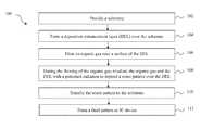
- FIG. 1illustrates a flow chart of a lithography patterning method according to various aspects of the present disclosure.
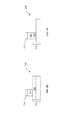
- FIGS. 2A, 2B, 2C, 2D, and 2Eillustrate cross sectional views of forming a target pattern according to the method of FIG. 1 , in accordance with an embodiment.
- FIGS. 3, 4A, 4B, and 4Cillustrate apparatuses that may be utilized by the method of FIG. 1 , in accordance with some embodiments.
- FIG. 5illustrates a flow chart of another lithography patterning method according to various aspects of the present disclosure.
- first and second featuresare formed in direct contact
- additional featuresmay be formed between the first and second features, such that the first and second features may not be in direct contact
- present disclosuremay repeat reference numerals and/or letters in the various examples. This repetition is for the purpose of simplicity and clarity and does not in itself dictate a relationship between the various embodiments and/or configurations discussed.
- spatially relative termssuch as “beneath,” “below,” “lower,” “above,” “upper” and the like, may be used herein for ease of description to describe one element or feature's relationship to another element(s) or feature(s) as illustrated in the figures.
- the spatially relative termsare intended to encompass different orientations of the device in use or operation in addition to the orientation depicted in the figures.
- the apparatusmay be otherwise oriented (rotated 90 degrees or at other orientations) and the spatially relative descriptors used herein may likewise be interpreted accordingly.
- the present disclosureis generally related to methods for semiconductor device fabrication, and more particularly to lithography patterning with a novel resist.
- the novel resistcomprises an organic gas.
- itis a gas phase resist.
- the novel resistis flowed, or otherwise supplied, to a patterning surface.
- traditional resist materialsare liquids and are typically spin-coated onto a patterning surface.
- the gas phase resistis irradiated with a patterned radiation, such as a patterned EUV radiation or a patterned electron beam (e-beam). Elements of the gas phase resist polymerize upon the radiation, thereby depositing a resist pattern over the patterning surface.
- the resist patternis deposited without such acid diffusion as in the case of CAR and does not undergo a developing process by a liquid developer. Therefore, the resist pattern has higher resolution and lower LER than traditional resist patterns, and does not suffer from the pattern collapsing issues associated with the traditional resist patterns.
- the resist patternis then used as an etch mask in subsequent etching processes, transferring the pattern to underlying patterning layers.
- the novel gas phase resist and the associated patterning processesare well-suited for advanced lithography processes including EUV lithography and e-beam lithography.
- FIG. 1is a flow chart of a method 100 of patterning a substrate (e.g., a semiconductor wafer) according to various aspects of the present disclosure.
- the method 100may be implemented, in whole or in part, by a system employing EUV lithography, e-beam lithography, and other advanced lithography processes to improve pattern dimension accuracy.
- EUV lithographyis used as the primary example. Additional operations can be provided before, during, and after the method 100 , and some operations described can be replaced, eliminated, or relocated for additional embodiments of the method.
- the method 100is an example, and is not intended to limit the present disclosure beyond what is explicitly recited in the claims. The method 100 is described below in conjunction with FIGS.
- the semiconductor device 200may be an intermediate device fabricated during processing of an IC, or a portion thereof, that may comprise SRAM and/or other logic circuits, passive components such as resistors, capacitors, and inductors, and active components such as p-type FETs (PFETs), n-type FETs (NFETs), fin-like FETs (FinFETs), other multi-gate FETs, metal-oxide semiconductor field effect transistors (MOSFET), complementary metal-oxide semiconductor (CMOS) transistors, bipolar transistors, high voltage transistors, high frequency transistors, other memory cells, and combinations thereof.
- PFETsp-type FETs
- NFETsn-type FETs
- FinFETsfin-like FETs
- MOSFETmetal-oxide semiconductor field effect transistors
- CMOScomplementary metal-oxide semiconductor
- the method 100( FIG. 1 ) is provided with a substrate 202 ( FIG. 2A ) at operation 102 .
- the substrate 202includes one or more layers of material or composition.
- the substrate 202is a semiconductor substrate (e.g., wafer).
- the substrate 202includes silicon in a crystalline structure.
- the substrate 202includes other elementary semiconductors such as germanium; a compound semiconductor including silicon carbide, gallium arsenic, gallium phosphide, indium phosphide, indium arsenide, and/or indium antimonide; an alloy semiconductor including SiGe, GaAsP, AlInAs, AlGaAs, GaInAs, GaInP, and/or GaInAsP; or combinations thereof.
- the substrate 202may include a silicon on insulator (SOI) substrate, be strained/stressed for performance enhancement, include epitaxial regions, include isolation regions, include doped regions, include one or more semiconductor devices or portions thereof, include conductive and/or non-conductive layers, and/or include other suitable features and layers.
- SOIsilicon on insulator
- the substrate 202includes a patterning layer 204 .
- the patterning layer 204is a hard mask layer including material(s) such as amorphous silicon (a-Si), silicon oxide, silicon nitride (SiN), titanium nitride, or other suitable materials or compositions.
- the patterning layer 204may include a dielectric layer such as a high-k dielectric layer, a gate layer, a hard mask layer, an interfacial layer, a capping layer, a diffusion barrier layer, a conductive layer, other suitable layers, and/or combinations thereof.
- the substrate 202is a mask substrate that may include a low thermal expansion material such as quartz, silicon, silicon carbide, or silicon oxide-titanium oxide compound.
- the substrate 202may be a mask substrate for making a deep ultraviolet (DUV) mask, an extreme ultraviolet (EUV) mask, or other types of masks.
- DUVdeep ultraviolet
- EUVextreme ultraviolet
- the method 100proceeds to operations 104 by forming a material layer 206 over the substrate 202 ( FIG. 2B ).
- the material layer 206is used for enhancing the deposition of the novel gas phase resist constructed according to the present disclosure. Therefore, the material layer 206 is also referred to as the deposition enhancement layer (DEL) 206 .
- the rate of the resist pattern depositiondepends on both the material of the gas phase resist and the material of the DEL 206 .
- the DEL 206has high absorption of a EUV radiation and is capable of generating secondary electrons when irradiated by the EUV radiation. The secondary electrons promote polymerization of the gas phase resist.
- the DEL 206comprises Ruthenium (Ru), such as a layer of the metal Ru.
- RuRuthenium
- the inventors of the present disclosurehave observed high deposition rate (or growth rate) of resist patterns over the DEL 206 comprising Ru.
- the DEL 206may comprise an oxide of the metal Ru or a metal complex having Ru atoms.
- the DEL 206may comprise a metal such as Ce, La, Sb, Pb, Hf, Zr, Ti, Cr, W, Mo, Fe, Os, Co, Rh, Ir, Ni, Pd, Pt, Cu, Ag, Au, Zn, Cd, Al, Ga, Tl, Ge, Sn, and Bi.
- the DEL 206may comprise a layer of the metal, an oxide of the metal, or a metal complex having atoms of the metal.
- the DEL 206comprises a polymer having a functional group selected from a group consisting of: —I, —Br, and —Cl. In another embodiment, the DEL 206 comprises a polymer having a functional group selected from a group consisting of: —NH 2 , —COOH, —OH, —SH, —N 3 , and —S( ⁇ O)—.
- the DEL 206comprises a polymer having a functional group selected from a group consisting of: alkene, alkyne, imine, ether, vinyl ether, acetal, hemiacetal, ester, aldehyde, ketone, amide, sulfone, acetic acid, cyanide, and allene.
- the polymermay have a non-cyclic structure or a cyclic structure, and the cyclic structure can be an aromatic ring or a non-aromatic ring.
- a thickness “H” of the DEL 206may be selected based on its intended use.
- the DEL 206is used primarily for depositing a resist pattern thereon, while the resist pattern is used as a primary etch mask for etching the substrate 202 .
- the DEL 206may be deposited as a relatively thin layer (e.g., “H” is 10 nanometers (nm) or less) so long as it sufficiently generates secondary electrons.
- the DEL 206is used not only for depositing a resist pattern thereon, but also as an etch mask for etching the substrate 202 .
- the DEL 206may be deposited as a relatively thick layer (e.g., “H” ranges from 30 nm to 50 nm) for the purpose of being an etch mask.
- the DEL 206may be formed over the substrate 202 using chemical vapor deposition (CVD), plasma enhanced CVD, physical vapor deposition (PVD), atomic layer deposition (ALD), spin-coating, plating, or other suitable deposition techniques, depending on the material(s) selected for the DEL 206 .
- CVDchemical vapor deposition
- PVDphysical vapor deposition
- ALDatomic layer deposition
- spin-coatingplating, or other suitable deposition techniques, depending on the material(s) selected for the DEL 206 .
- the method 100proceeds to operation 106 by flowing or supplying an organic gas 212 near a top surface of the DEL 206 ( FIG. 2C ).
- the organic gas 212flows through a supply pipe 210 which is configured to control the flow rate and the flow direction of the organic gas 212 .
- Elements of the organic gas 212adsorb to the surface of the DEL 206 and further spread out in an area near the vicinity of the point of supply.
- the method 100proceeds to operation 108 to irradiate the organic gas 212 and the DEL 206 with a patterned radiation (or a patterned radiation beam) 208 ( FIG. 2C ).
- a patterned radiationor a patterned radiation beam
- the patterned radiation 208 , the organic gas 212 , and the DEL 206collectively deposit a resist pattern 214 over the DEL 206 .
- the mechanism of the depositionmay be explained as follows.
- the radiation 208is a highly energetic radiation such as a EUV ray or an e-beam.
- the DEL 206absorbs some of the energy of the radiation 208 , thereby generating secondary electrons.
- the organic gas 212undergoes polymerization reaction after being exposed to the radiation 208 .
- the polymerization reactionmay be promoted and enhanced by the secondary electrons released from the DEL 206 .
- the polymerization reactionleads to the deposition of the resist pattern 214 .
- the radiation 208is patterned with a pattern of an IC design layout, for example, through the use of a EUV mask or of a maskless patterning process. Thus, only certain areas of the surface of the DEL 206 are irradiated by the radiation 208 and, in these areas, so deposited the resist pattern 214 .
- the organic gas 212comprises reactive sites or cross-linkable groups that make polymerization possible. Some elements of the organic gas 212 may be photo-sensitive. For example, they may absorb the radiation 208 and generate secondary electrons.
- the organic gas 212comprises an organic molecule having one or more cross-linkable groups.
- the cross-linkable groupsmay include a C 3 -C 20 alkyl group (an alkyl group having three to twenty carbon atoms) having at least one light-sensitive functional group.
- the light-sensitive functional groupis selected from a group consisting of epoxy, azo compounds, alkyl halide, imine, alkene, alkyne, peroxide, ketone, aldehyde, allene, aromatic groups, and heterocyclic groups.
- the aromatic groupsmay comprise phenyl, napthlenyl, phenanthrenyl, anthracenyl, phenalynyl, and other aromatic derivatives having one to five-membered rings.
- the organic gas 212comprises an organic molecule that has a functional group selected from a group consisting of: —I, —Br, and —Cl. In another embodiment, the organic gas 212 comprises an organic molecule that has a functional group selected from a group consisting of: —NH 2 , —COOH, —OH, —SH, —N 3 , and —S( ⁇ O)—.
- the organic gas 212comprises an organic molecule that has a functional group selected from a group consisting of: alkene, alkyne, imine, ether, vinyl ether, acetal, hemiacetal, ester, aldehyde, ketone, amide, sulfone, acetic acid, cyanide, and allene.
- the chemical structure of the molecules of the organic gas 212can be cyclic or non-cyclic.
- the cyclic structurecan be an aromatic ring or a non-aromatic ring.
- the organic gas 212comprises a metal complex wherein metal atoms of the metal complex may be selected from a group consisting of Ce, La, Sb, Bi, Pb, Hf, Zr, Ti, Cr, W, Mo, Fe, Ru, Os, Co, Rh, Ir, Ni, Pd, Pt, Cu, Ag, Au, Zn, Cd, Al, Ga, Tl, Ge, and Sn.
- a ligand of the metal complexhas a functional group selected from a group consisting of: —I, —Br, and —Cl.
- the ligand of the metal complexhas a functional group selected from a group consisting of: —NH 2 , —COOH, —OH, —SH, —N 3 , and —S( ⁇ O)—.
- the ligand of the metal complexhas a functional group selected from a group consisting of: alkene, alkyne, imine, ether, vinyl ether, acetal, hemiacetal, ester, aldehyde, ketone, amide, sulfone, acetic acid, cyanide, and allene.
- the molecular weight of the organic gas 212may range from 30 to 10,000 g/mol.
- the flow rate of the organic gas 212is selected to facilitate volume production.
- the flow rate of the organic gas 212may be selected in a range from 10,000 to 100,000 standard cubic centimeters per minute (sccm).
- the flow rate of the organic gas 212may range from 10 to 100,000 sccm.
- the formation of the resist pattern 214does not undergo an acid diffusion process associated with traditional CAR-based resist patterns. Therefore, it provides finer resolution and smoother edges and sidewalls than the traditional CAR-based resist patterns. Furthermore, the resist pattern 214 is directly deposited over the substrate 202 without being developed by an aqueous developer, thereby reducing the likelihood of pattern collapsing issues seen with the traditional CAR-based resist patterns.
- operation 110includes etching the DEL 206 with the resist pattern 214 as an etch mask, thereby forming a patterned DEL 206 ( FIG. 2D ).
- the resist pattern 214may be partially consumed during this operation.
- operation 110further includes etching the substrate 202 with the patterned DEL 206 , and possibly the resist pattern 214 as well, as an etch mask ( FIG. 2E ).
- operation 110includes etching both the DEL 206 and the substrate 202 using the resist pattern 214 as an etch mask.
- the patternis transferred from the resist pattern 214 to the patterning layer 204 of the substrate 202 ( FIG. 2E ).
- the etching of the DEL 206 and the substrate 202may use a dry (plasma) etching, a wet etching, and/or other etching methods.
- a dry etching processmay implement an oxygen-containing gas, a fluorine-containing gas (e.g., CF 4 , SF 6 , CH 2 F 2 , CHF 3 , and/or C 2 F 6 ), a chlorine-containing gas (e.g., Cl 2 , CHCl 3 , CCl 4 , and/or BCl 3 ), a bromine-containing gas (e.g., HBr and/or CHBR 3 ), an iodine-containing gas, other suitable gases and/or plasmas, and/or combinations thereof.
- a fluorine-containing gase.g., CF 4 , SF 6 , CH 2 F 2 , CHF 3 , and/or C 2 F 6
- a chlorine-containing gase.g., Cl 2 , CHCl 3 , CCl 4 , and/or BCl 3
- a bromine-containing gase.g., HBr and/or CHBR 3
- a wet etching processmay comprise etching in diluted hydrofluoric acid (DHF); potassium hydroxide (KOH) solution; ammonia; a solution containing hydrofluoric acid (HF), nitric acid (HNO 3 ), and/or acetic acid (CH 3 COOH); or other suitable wet etchant.
- DHFdiluted hydrofluoric acid
- KOHpotassium hydroxide
- ammoniaa solution containing hydrofluoric acid (HF), nitric acid (HNO 3 ), and/or acetic acid (CH 3 COOH); or other suitable wet etchant.
- the resist pattern 214may be partially or completely consumed during the etching of the DEL 206 and the patterning layer 204 .
- the method 100proceeds to operation 112 to form a final pattern or an IC device on the substrate 202 .
- the substrate 202is a semiconductor substrate and the method 100 proceeds to forming fin field effect transistor (FinFET) structures.
- operation 112forms a plurality of active fins in the semiconductor substrate 202 .
- the active finshave uniform width and length due to the smooth edges and sidewalls of the resist pattern 214 .
- the method 100proceeds to forming a plurality of gate electrodes in the semiconductor substrate 202 .
- the gate electrodeshave uniform gate length due to the quality of the resist pattern 214 .
- the method 100may further form gate spacers, source/drain regions, contacts for gate/source/drain features, etc.
- a target patternis to be formed as metal lines in a multilayer interconnection structure.
- the metal linesmay be formed in an inter-layer dielectric (ILD) layer of the substrate 202 , which has been etched by operation 110 to include a plurality of trenches.
- the method 100proceeds to filling the trenches with a conductive material, such as a metal; and polishing the conductive material using a process such as chemical mechanical planarization (CMP) to expose the patterned ILD layer, thereby forming the metal lines in the ILD layer.
- CMPchemical mechanical planarization
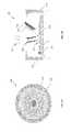
- FIG. 3is a schematic view of a EUV lithography system 300 , according to aspects of the present disclosure.
- the EUV lithography system 300may be used for performing some operations of the method 100 , such as the operations 106 and 108 .
- the EUV lithography system 300includes a radiation source 302 that produces the radiation 208 , condenser optics 306 , a mask stage 310 securing a EUV mask 308 thereon, projection optics 312 , and a substrate stage 314 securing the device 200 including the substrate 202 and the DEL 206 .
- the EUV lithography system 300further includes the supply pipe 210 for supplying the organic gas 212 near a top surface of the DEL 206 .
- the EUV lithography system 300may be a stepper or a scanner. The various components of the EUV lithography system 300 are briefly described below.
- the radiation source 302provides the radiation 208 having a wavelength in the EUV range, such as about 1-100 nm. In one example, the radiation 208 has a wavelength of about 13.5 nm. In embodiments, the radiation source 302 may use laser produced plasma (LPP) to generate the radiation 208 .
- the condenser optics 306includes a multilayer coated collector and a plurality of grazing mirrors. The condenser optics 306 is configured to collect and shape the radiation 208 and to provide a slit of the radiation 208 to the mask 308 .
- the mask 308also referred to as a photomask or a reticle, includes patterns of one or more target IC devices.
- the mask 308provides a patterned aerial image to the radiation 208 , which then becomes a patterned radiation 208 .
- the mask 308is a reflective mask in the present embodiment, and may incorporate resolution enhancement techniques such as phase-shifting techniques and/or optical proximity correction.
- the mask stage 310secures the mask 308 thereon, such as by vacuum, and provides accurate position and movement of the mask 308 during alignment, focus, leveling, and deposition operation in the EUV lithography system 300 .
- the projection optics 312includes one or more lens and a plurality of mirrors.
- the lensmay have a magnification of less than one thereby reducing the patterned aerial image of the mask 308 to the device 200 , particularly, to the DEL 206 .
- the device 200is secured by the substrate stage 314 which provides accurate position and movement of the device 200 during alignment, focus, leveling, and deposition operation in the EUV lithography system 300 such that the patterned aerial image of the mask 308 is irradiated onto the DEL 206 .
- the substrate stage 314can further move the device 200 relative to the supply pipe 210 and the patterned radiation 208 so that the resist pattern 214 is deposited (or grown) across an area of the DEL 206 .
- FIGS. 4A, 4B, and 4Cfurther illustrate some components of the EUV lithography system 300 and the movements thereof in depositing the resist pattern 214 across a top surface of the device 200 .
- FIG. 4Ashows a top view of the EUV lithography system 300 , in portion, while FIGS. 4B and 4C illustrate side views of the EUV lithography system 300 .
- the EUV lithography system 300includes a slit sensor 316 for monitoring the energy level of the radiation beam 208 .
- the slit sensor 316is integrated with the substrate stage 314 at a place near an edge of the device 200 (e.g., a wafer).
- the EUV lithography system 300further includes a mechanism for supplying a gas flow 318 which is hydrogen gas in the present embodiment. Hydrogen gas has less absorption to the EUV radiation 208 and can be used for reducing contamination of the various components of the EUV lithography system 300 ( FIG. 3 ) by the byproducts of the polymerization reaction.
- the EUV lithography system 300further includes a supply pipe 320 which is to flow a gas 322 ( FIG. 4C ) to the surface of the DEL 206 .
- the gas 322is hydrogen gas.
- the supply pipe 320is configured to work in conjunction with the supply pipe 210 and the patterned radiation 208 to reduce contamination of the slit sensor 316 , as explained in the next paragraph.
- the EUV lithography system 300further includes an exhaust line 324 for discharging the gaseous waste and/or contaminants out of the EUV lithography system 300 .
- the exhaust line 324is configured around the substrate stage 314 , and the contaminants are discharged through the exhaust line 324 and through the gap between the exhaust line 324 and the substrate stage 314 .
- the patterned radiation 208irradiates an area of the device 200 (having the DEL 206 as its top layer), for example, at or near the center of the device 200 .
- the supply pipe 210flows the organic gas 212 towards the vicinity of the same area.
- the resist pattern 214FIG. 2C
- the supply pipe 320is shut off at this time, i.e., it does not supply the gas 322 to the surface of the device 200 .
- the device 200is moved relative to the radiation 208 and the supply pipes 210 and 320 such that the resist pattern 214 is deposited across an area of the device 200 according to the IC pattern to be transferred.
- the movement of the device 200may be carried out by the substrate stage 314 .
- the supply pipe 210is shut off and the supply pipe 320 is turned on.
- the gas 322e.g., hydrogen gas
- the gas 322flows to the surface of the device 200 to purge it of any organic gas residues.
- the resist pattern 214is not deposited in the area between D and E, including at the edge E.
- the radiation 208is at or near the slit sensor 316
- there is no organic gas 212 or only insignificant amount of organic gas 212 present in the vicinity of the slit sensor 316This advantageously prevents the slit sensor 316 from being contaminated by the organic gas 212 or its derivatives.
- FIG. 5shows a method 400 for lithography patterning using a lithography system, such as the EUV lithography system 300 .
- the method 400is briefly discussed below using the EUV lithography system 300 as the exemplary system.
- the method 400secures a substrate 200 (e.g., a wafer) on a substrate stage 314 (e.g., FIG. 4A ).
- the substrate 200has a DEL 206 as its top layer.
- the method 400directs a patterned radiation 208 towards a surface of the substrate 200 (e.g., FIG. 4B ).
- the method 400flows an organic gas 212 near the surface of the substrate 200 (e.g., FIG. 4B ).
- a resist pattern 214e.g., FIG. 2C , is deposited over the substrate 200 .
- the method 400moves the substrate 200 relative to the patterned radiation 208 so as to scan an area of the substrate. The movement is driven by the substrate stage 314 .
- the organic gas flow 212is supplied through a supply pipe whose position may be fixed relative to the patterned radiation 208 .
- the method 400stops the organic gas flow before the resist pattern 214 is deposited at an edge of the substrate 200 .
- the method 400further includes flowing hydrogen gas to the surface of the substrate when the organic gas flow is stopped.
- the method 400controls where the resist pattern 214 is to be formed or deposited.
- traditional CAR-based resistis spin-coated onto the entire surface of the substrate 200 .
- thickness of such spin-coated resist layeris not uniform across the surface, especially between the center and the edge of the substrate 200 .
- the non-uniform thicknessmay lead to patterning issues, such as over-exposure, under-exposure, over-development, and/or under-development.
- the method 400overcomes such issues because, among other factors, the resist pattern 214 is only formed where it is desired, such as away from the edges, and the resist pattern 214 is directly deposited and does not undergo a developing process.
- a resist pattern formed according to the present disclosureprovides smooth edges and sidewalls with near uniform critical dimensions, which is highly desirable for advanced lithography, such as EUV lithography or e-beam lithography.
- Embodiments of the present disclosureenable the deposition of a resist pattern in selected areas of a substrate, thereby reducing the costs associated with resist material and resist developing processes.
- the present disclosureis directed to a method for lithography patterning.
- the methodincludes providing a substrate, forming a deposition enhancement layer (DEL) over the substrate, and flowing an organic gas near a surface of the DEL.
- the methodfurther includes irradiating the DEL and the organic gas with a patterned radiation. Elements of the organic gas polymerize upon the patterned radiation, thereby forming a resist pattern over the DEL.
- the methodfurther includes etching the DEL with the resist pattern as an etch mask, thereby forming a patterned DEL.
- the methodfurther includes etching the substrate with at least one of the patterned DEL and the resist pattern as an etch mask.
- the present disclosureis directed to an apparatus for lithography patterning.
- the apparatusincludes a mechanism for producing a patterned radiation beam, a substrate stage configured to hold a substrate, a first supply pipe for flowing an organic gas near a surface of the substrate, and a second supply pipe for flowing hydrogen gas near the surface of the substrate.
- the first supply pipeis configured to flow the organic gas while the patterned radiation beam scans the surface of the substrate and to shut off the flowing of the organic gas before the patterned radiation beam reaches an edge of the substrate.
- the second supply pipeis configured to flow the hydrogen gas when the first supply pipe is shut off and to shut off the flowing of the hydrogen gas when the first supply pipe flows the organic gas.
- the patterned radiation beamcauses the organic gas to polymerize, thereby depositing a resist pattern over the substrate.
- the present disclosureis directed to a method for lithography patterning.
- the methodincludes directing a patterned radiation towards a surface of a substrate and supplying an organic gas near the surface of the substrate. Elements of the organic gas polymerize upon the patterned radiation, thereby forming a resist pattern over the surface of the substrate.
- the methodfurther includes moving the substrate relative to the patterned radiation such that the resist pattern is formed across an area of the substrate.
- the methodfurther includes stopping the supplying of the organic gas when the resist pattern is formed near an edge of the substrate.
- the methodfurther includes flowing hydrogen gas after the stopping of the supplying of the organic gas.
Landscapes
- Physics & Mathematics (AREA)
- Engineering & Computer Science (AREA)
- General Physics & Mathematics (AREA)
- Power Engineering (AREA)
- Condensed Matter Physics & Semiconductors (AREA)
- Manufacturing & Machinery (AREA)
- Computer Hardware Design (AREA)
- Microelectronics & Electronic Packaging (AREA)
- Chemical & Material Sciences (AREA)
- Plasma & Fusion (AREA)
- Chemical Kinetics & Catalysis (AREA)
- Toxicology (AREA)
- Health & Medical Sciences (AREA)
- Architecture (AREA)
- Structural Engineering (AREA)
- General Chemical & Material Sciences (AREA)
- Organic Chemistry (AREA)
- Spectroscopy & Molecular Physics (AREA)
- Inorganic Chemistry (AREA)
- General Health & Medical Sciences (AREA)
- Exposure And Positioning Against Photoresist Photosensitive Materials (AREA)
- Exposure Of Semiconductors, Excluding Electron Or Ion Beam Exposure (AREA)
Abstract
Description
The semiconductor integrated circuit (IC) industry has experienced rapid growth in the past several decades. Technological advances in semiconductor materials and design have produced increasingly smaller and more complex circuits. These material and design advances have been made possible as the technologies related to processing and manufacturing have also undergone technical advances. As a size of the smallest component has decreased, numerous challenges have arisen. For example, the need to perform higher resolution lithography patterning grows.
Techniques such as extreme ultraviolet (EUV) lithography have been utilized to support high resolution requirements of nano-scale semiconductor devices. EUV lithography employs radiations in the EUV region, having a wavelength of about 1-100 nm, thereby providing finer resolution than traditional radiation sources such as KrF and ArF. However, realizing all the benefits that EUV lithography can offer remains challenging. One challenge is in the resist materials and the resist patterning processes used for EUV lithography.
A commonly used resist material for lithography is a chemically amplified resist (CAR) that contains backbone polymer protected by acid labile groups (ALGs). CAR further contains photo-acid generators which, upon radiation, produce an acid. The acid can catalyze the cleaving of the ALGs from the backbone polymer, such as in a post exposure bake process. The de-protected portion of the resist is dissolved in a liquid developer, leaving the remaining portion of the resist as a resist pattern. Issues may arise during the exposure and development of the resist. For example, diffusion of the acid during the exposure may lead to blurring of the edges of the patterned areas, thus limiting the resolution and line edge roughness (LER) of the resist pattern. For example, when the exposed resist is developed in a liquid developer, the resist pattern may collapse due to its high aspect ratio and the developer's surface tension.
Accordingly, a new resist and the associated patterning processes are desired.
The present disclosure is best understood from the following detailed description when read with the accompanying figures. It is emphasized that, in accordance with the standard practice in the industry, various features are not drawn to scale and are used for illustration purposes only. In fact, the dimensions of the various features may be arbitrarily increased or reduced for clarity of discussion.
The following disclosure provides many different embodiments, or examples, for implementing different features of the provided subject matter. Specific examples of components and arrangements are described below to simplify the present disclosure. These are, of course, merely examples and are not intended to be limiting. For example, the formation of a first feature over or on a second feature in the description that follows may include embodiments in which the first and second features are formed in direct contact, and may also include embodiments in which additional features may be formed between the first and second features, such that the first and second features may not be in direct contact. In addition, the present disclosure may repeat reference numerals and/or letters in the various examples. This repetition is for the purpose of simplicity and clarity and does not in itself dictate a relationship between the various embodiments and/or configurations discussed.
Further, spatially relative terms, such as “beneath,” “below,” “lower,” “above,” “upper” and the like, may be used herein for ease of description to describe one element or feature's relationship to another element(s) or feature(s) as illustrated in the figures. The spatially relative terms are intended to encompass different orientations of the device in use or operation in addition to the orientation depicted in the figures. The apparatus may be otherwise oriented (rotated 90 degrees or at other orientations) and the spatially relative descriptors used herein may likewise be interpreted accordingly.
The present disclosure is generally related to methods for semiconductor device fabrication, and more particularly to lithography patterning with a novel resist. According to aspects of the present disclosure, the novel resist comprises an organic gas. Thus, it is a gas phase resist. The novel resist is flowed, or otherwise supplied, to a patterning surface. In contrast, traditional resist materials are liquids and are typically spin-coated onto a patterning surface. According to aspects of the present disclosure, the gas phase resist is irradiated with a patterned radiation, such as a patterned EUV radiation or a patterned electron beam (e-beam). Elements of the gas phase resist polymerize upon the radiation, thereby depositing a resist pattern over the patterning surface. According to embodiments of the present disclosure, the resist pattern is deposited without such acid diffusion as in the case of CAR and does not undergo a developing process by a liquid developer. Therefore, the resist pattern has higher resolution and lower LER than traditional resist patterns, and does not suffer from the pattern collapsing issues associated with the traditional resist patterns. The resist pattern is then used as an etch mask in subsequent etching processes, transferring the pattern to underlying patterning layers. The novel gas phase resist and the associated patterning processes are well-suited for advanced lithography processes including EUV lithography and e-beam lithography.
The method100 (FIG. 1 ) is provided with a substrate202 (FIG. 2A ) atoperation 102. Referring toFIG. 2A , thesubstrate 202 includes one or more layers of material or composition. In an embodiment, thesubstrate 202 is a semiconductor substrate (e.g., wafer). In another embodiment, thesubstrate 202 includes silicon in a crystalline structure. In alternative embodiments, thesubstrate 202 includes other elementary semiconductors such as germanium; a compound semiconductor including silicon carbide, gallium arsenic, gallium phosphide, indium phosphide, indium arsenide, and/or indium antimonide; an alloy semiconductor including SiGe, GaAsP, AlInAs, AlGaAs, GaInAs, GaInP, and/or GaInAsP; or combinations thereof. Thesubstrate 202 may include a silicon on insulator (SOI) substrate, be strained/stressed for performance enhancement, include epitaxial regions, include isolation regions, include doped regions, include one or more semiconductor devices or portions thereof, include conductive and/or non-conductive layers, and/or include other suitable features and layers.
In the present embodiment, thesubstrate 202 includes apatterning layer 204. In an embodiment, thepatterning layer 204 is a hard mask layer including material(s) such as amorphous silicon (a-Si), silicon oxide, silicon nitride (SiN), titanium nitride, or other suitable materials or compositions. In various embodiments, thepatterning layer 204 may include a dielectric layer such as a high-k dielectric layer, a gate layer, a hard mask layer, an interfacial layer, a capping layer, a diffusion barrier layer, a conductive layer, other suitable layers, and/or combinations thereof.
In another embodiment, thesubstrate 202 is a mask substrate that may include a low thermal expansion material such as quartz, silicon, silicon carbide, or silicon oxide-titanium oxide compound. To further this example, thesubstrate 202 may be a mask substrate for making a deep ultraviolet (DUV) mask, an extreme ultraviolet (EUV) mask, or other types of masks.
The method100 (FIG. 1 ) proceeds tooperations 104 by forming amaterial layer 206 over the substrate202 (FIG. 2B ). In the present embodiment, thematerial layer 206 is used for enhancing the deposition of the novel gas phase resist constructed according to the present disclosure. Therefore, thematerial layer 206 is also referred to as the deposition enhancement layer (DEL)206. In some embodiments, the rate of the resist pattern deposition depends on both the material of the gas phase resist and the material of theDEL 206. In embodiments, theDEL 206 has high absorption of a EUV radiation and is capable of generating secondary electrons when irradiated by the EUV radiation. The secondary electrons promote polymerization of the gas phase resist.
In an embodiment, theDEL 206 comprises Ruthenium (Ru), such as a layer of the metal Ru. The inventors of the present disclosure have observed high deposition rate (or growth rate) of resist patterns over theDEL 206 comprising Ru. In alternative embodiments, theDEL 206 may comprise an oxide of the metal Ru or a metal complex having Ru atoms. Alternatively or additionally, theDEL 206 may comprise a metal such as Ce, La, Sb, Pb, Hf, Zr, Ti, Cr, W, Mo, Fe, Os, Co, Rh, Ir, Ni, Pd, Pt, Cu, Ag, Au, Zn, Cd, Al, Ga, Tl, Ge, Sn, and Bi. For example, theDEL 206 may comprise a layer of the metal, an oxide of the metal, or a metal complex having atoms of the metal.
In an embodiment, theDEL 206 comprises a polymer having a functional group selected from a group consisting of: —I, —Br, and —Cl. In another embodiment, theDEL 206 comprises a polymer having a functional group selected from a group consisting of: —NH2, —COOH, —OH, —SH, —N3, and —S(═O)—. In yet another embodiment, theDEL 206 comprises a polymer having a functional group selected from a group consisting of: alkene, alkyne, imine, ether, vinyl ether, acetal, hemiacetal, ester, aldehyde, ketone, amide, sulfone, acetic acid, cyanide, and allene. In each of the above embodiments, the polymer may have a non-cyclic structure or a cyclic structure, and the cyclic structure can be an aromatic ring or a non-aromatic ring.
In embodiments, a thickness “H” of theDEL 206 may be selected based on its intended use. In an embodiment, theDEL 206 is used primarily for depositing a resist pattern thereon, while the resist pattern is used as a primary etch mask for etching thesubstrate 202. To further this embodiment, theDEL 206 may be deposited as a relatively thin layer (e.g., “H” is 10 nanometers (nm) or less) so long as it sufficiently generates secondary electrons. In another embodiment, theDEL 206 is used not only for depositing a resist pattern thereon, but also as an etch mask for etching thesubstrate 202. To further this embodiment, theDEL 206 may be deposited as a relatively thick layer (e.g., “H” ranges from 30 nm to 50 nm) for the purpose of being an etch mask.
In some embodiments, theDEL 206 may be formed over thesubstrate 202 using chemical vapor deposition (CVD), plasma enhanced CVD, physical vapor deposition (PVD), atomic layer deposition (ALD), spin-coating, plating, or other suitable deposition techniques, depending on the material(s) selected for theDEL 206.
The method100 (FIG. 1 ) proceeds tooperation 106 by flowing or supplying anorganic gas 212 near a top surface of the DEL206 (FIG. 2C ). ReferringFIG. 2C , in the present embodiment, theorganic gas 212 flows through asupply pipe 210 which is configured to control the flow rate and the flow direction of theorganic gas 212. Elements of theorganic gas 212 adsorb to the surface of theDEL 206 and further spread out in an area near the vicinity of the point of supply.
While theorganic gas 212 is being supplied to the surface of theDEL 206, the method100 (FIG. 1 ) proceeds tooperation 108 to irradiate theorganic gas 212 and theDEL 206 with a patterned radiation (or a patterned radiation beam)208 (FIG. 2C ). ReferringFIG. 2C , the patternedradiation 208, theorganic gas 212, and theDEL 206 collectively deposit a resistpattern 214 over theDEL 206. The mechanism of the deposition may be explained as follows. In an embodiment, theradiation 208 is a highly energetic radiation such as a EUV ray or an e-beam. TheDEL 206 absorbs some of the energy of theradiation 208, thereby generating secondary electrons. Meanwhile, theorganic gas 212 undergoes polymerization reaction after being exposed to theradiation 208. The polymerization reaction may be promoted and enhanced by the secondary electrons released from theDEL 206. The polymerization reaction leads to the deposition of the resistpattern 214. Furthermore, theradiation 208 is patterned with a pattern of an IC design layout, for example, through the use of a EUV mask or of a maskless patterning process. Thus, only certain areas of the surface of theDEL 206 are irradiated by theradiation 208 and, in these areas, so deposited the resistpattern 214.
In embodiments, theorganic gas 212 comprises reactive sites or cross-linkable groups that make polymerization possible. Some elements of theorganic gas 212 may be photo-sensitive. For example, they may absorb theradiation 208 and generate secondary electrons. In an embodiment, theorganic gas 212 comprises an organic molecule having one or more cross-linkable groups. For example, the cross-linkable groups may include a C3-C20alkyl group (an alkyl group having three to twenty carbon atoms) having at least one light-sensitive functional group. In a further embodiment, the light-sensitive functional group is selected from a group consisting of epoxy, azo compounds, alkyl halide, imine, alkene, alkyne, peroxide, ketone, aldehyde, allene, aromatic groups, and heterocyclic groups. Furthermore, the aromatic groups may comprise phenyl, napthlenyl, phenanthrenyl, anthracenyl, phenalynyl, and other aromatic derivatives having one to five-membered rings.
In an embodiment, theorganic gas 212 comprises an organic molecule that has a functional group selected from a group consisting of: —I, —Br, and —Cl. In another embodiment, theorganic gas 212 comprises an organic molecule that has a functional group selected from a group consisting of: —NH2, —COOH, —OH, —SH, —N3, and —S(═O)—. In yet another embodiment, theorganic gas 212 comprises an organic molecule that has a functional group selected from a group consisting of: alkene, alkyne, imine, ether, vinyl ether, acetal, hemiacetal, ester, aldehyde, ketone, amide, sulfone, acetic acid, cyanide, and allene. The chemical structure of the molecules of theorganic gas 212 can be cyclic or non-cyclic. The cyclic structure can be an aromatic ring or a non-aromatic ring.
In another embodiment, theorganic gas 212 comprises a metal complex wherein metal atoms of the metal complex may be selected from a group consisting of Ce, La, Sb, Bi, Pb, Hf, Zr, Ti, Cr, W, Mo, Fe, Ru, Os, Co, Rh, Ir, Ni, Pd, Pt, Cu, Ag, Au, Zn, Cd, Al, Ga, Tl, Ge, and Sn. To further this embodiment, a ligand of the metal complex has a functional group selected from a group consisting of: —I, —Br, and —Cl. In an alternative embodiment, the ligand of the metal complex has a functional group selected from a group consisting of: —NH2, —COOH, —OH, —SH, —N3, and —S(═O)—. In yet another alternative embodiment, the ligand of the metal complex has a functional group selected from a group consisting of: alkene, alkyne, imine, ether, vinyl ether, acetal, hemiacetal, ester, aldehyde, ketone, amide, sulfone, acetic acid, cyanide, and allene.
In various embodiments, the molecular weight of theorganic gas 212 may range from 30 to 10,000 g/mol. In embodiments, the flow rate of theorganic gas 212 is selected to facilitate volume production. For example, the flow rate of theorganic gas 212 may be selected in a range from 10,000 to 100,000 standard cubic centimeters per minute (sccm). In various embodiments, the flow rate of theorganic gas 212 may range from 10 to 100,000 sccm. The inventors of the present disclosure have observed that a higher pressure of theorganic gas 212 in the deposition environment generally leads to faster deposition of the resistpattern 214, and that a higher flow rate of theorganic gas 212 generally leads to a higher pressure thereof.
As discussed above, the formation of the resistpattern 214 does not undergo an acid diffusion process associated with traditional CAR-based resist patterns. Therefore, it provides finer resolution and smoother edges and sidewalls than the traditional CAR-based resist patterns. Furthermore, the resistpattern 214 is directly deposited over thesubstrate 202 without being developed by an aqueous developer, thereby reducing the likelihood of pattern collapsing issues seen with the traditional CAR-based resist patterns.
The method100 (FIG. 1 ) proceeds tooperation 110 to transfer the pattern from the resistpattern 214 to thesubstrate 202. In an embodiment,operation 110 includes etching theDEL 206 with the resistpattern 214 as an etch mask, thereby forming a patterned DEL206 (FIG. 2D ). The resistpattern 214 may be partially consumed during this operation. Thereafter,operation 110 further includes etching thesubstrate 202 with the patternedDEL 206, and possibly the resistpattern 214 as well, as an etch mask (FIG. 2E ). In another embodiment,operation 110 includes etching both theDEL 206 and thesubstrate 202 using the resistpattern 214 as an etch mask.
As a result of theoperation 110, the pattern is transferred from the resistpattern 214 to thepatterning layer 204 of the substrate202 (FIG. 2E ). The etching of theDEL 206 and thesubstrate 202 may use a dry (plasma) etching, a wet etching, and/or other etching methods. For example, a dry etching process may implement an oxygen-containing gas, a fluorine-containing gas (e.g., CF4, SF6, CH2F2, CHF3, and/or C2F6), a chlorine-containing gas (e.g., Cl2, CHCl3, CCl4, and/or BCl3), a bromine-containing gas (e.g., HBr and/or CHBR3), an iodine-containing gas, other suitable gases and/or plasmas, and/or combinations thereof. For example, a wet etching process may comprise etching in diluted hydrofluoric acid (DHF); potassium hydroxide (KOH) solution; ammonia; a solution containing hydrofluoric acid (HF), nitric acid (HNO3), and/or acetic acid (CH3COOH); or other suitable wet etchant. The resistpattern 214 may be partially or completely consumed during the etching of theDEL 206 and thepatterning layer 204.
The method100 (FIG. 1 ) proceeds tooperation 112 to form a final pattern or an IC device on thesubstrate 202. In an embodiment, thesubstrate 202 is a semiconductor substrate and themethod 100 proceeds to forming fin field effect transistor (FinFET) structures. In this embodiment,operation 112 forms a plurality of active fins in thesemiconductor substrate 202. The active fins have uniform width and length due to the smooth edges and sidewalls of the resistpattern 214. In another embodiment, themethod 100 proceeds to forming a plurality of gate electrodes in thesemiconductor substrate 202. The gate electrodes have uniform gate length due to the quality of the resistpattern 214. Themethod 100 may further form gate spacers, source/drain regions, contacts for gate/source/drain features, etc. In another embodiment, a target pattern is to be formed as metal lines in a multilayer interconnection structure. For example, the metal lines may be formed in an inter-layer dielectric (ILD) layer of thesubstrate 202, which has been etched byoperation 110 to include a plurality of trenches. Themethod 100 proceeds to filling the trenches with a conductive material, such as a metal; and polishing the conductive material using a process such as chemical mechanical planarization (CMP) to expose the patterned ILD layer, thereby forming the metal lines in the ILD layer. The above are non-limiting examples of devices/structures that can be made and/or improved using themethod 100 according to various aspects of the present disclosure.
Theradiation source 302 provides theradiation 208 having a wavelength in the EUV range, such as about 1-100 nm. In one example, theradiation 208 has a wavelength of about 13.5 nm. In embodiments, theradiation source 302 may use laser produced plasma (LPP) to generate theradiation 208. Thecondenser optics 306 includes a multilayer coated collector and a plurality of grazing mirrors. Thecondenser optics 306 is configured to collect and shape theradiation 208 and to provide a slit of theradiation 208 to themask 308. Themask 308, also referred to as a photomask or a reticle, includes patterns of one or more target IC devices. Themask 308 provides a patterned aerial image to theradiation 208, which then becomes apatterned radiation 208. Themask 308 is a reflective mask in the present embodiment, and may incorporate resolution enhancement techniques such as phase-shifting techniques and/or optical proximity correction. Themask stage 310 secures themask 308 thereon, such as by vacuum, and provides accurate position and movement of themask 308 during alignment, focus, leveling, and deposition operation in theEUV lithography system 300.
Theprojection optics 312 includes one or more lens and a plurality of mirrors. The lens may have a magnification of less than one thereby reducing the patterned aerial image of themask 308 to thedevice 200, particularly, to theDEL 206. Thedevice 200 is secured by thesubstrate stage 314 which provides accurate position and movement of thedevice 200 during alignment, focus, leveling, and deposition operation in theEUV lithography system 300 such that the patterned aerial image of themask 308 is irradiated onto theDEL 206. Thesubstrate stage 314 can further move thedevice 200 relative to thesupply pipe 210 and the patternedradiation 208 so that the resistpattern 214 is deposited (or grown) across an area of theDEL 206.
Referring toFIGS. 4A, 4B, and 4C collectively, theEUV lithography system 300 includes aslit sensor 316 for monitoring the energy level of theradiation beam 208. In this embodiment, theslit sensor 316 is integrated with thesubstrate stage 314 at a place near an edge of the device200 (e.g., a wafer). TheEUV lithography system 300 further includes a mechanism for supplying agas flow 318 which is hydrogen gas in the present embodiment. Hydrogen gas has less absorption to theEUV radiation 208 and can be used for reducing contamination of the various components of the EUV lithography system300 (FIG. 3 ) by the byproducts of the polymerization reaction. TheEUV lithography system 300 further includes asupply pipe 320 which is to flow a gas322 (FIG. 4C ) to the surface of theDEL 206. In this embodiment, thegas 322 is hydrogen gas. In the present embodiment, thesupply pipe 320 is configured to work in conjunction with thesupply pipe 210 and the patternedradiation 208 to reduce contamination of theslit sensor 316, as explained in the next paragraph. Also shown inFIGS. 4A-4C , theEUV lithography system 300 further includes anexhaust line 324 for discharging the gaseous waste and/or contaminants out of theEUV lithography system 300. In the present embodiment, theexhaust line 324 is configured around thesubstrate stage 314, and the contaminants are discharged through theexhaust line 324 and through the gap between theexhaust line 324 and thesubstrate stage 314.
As shown inFIG. 4B , the patternedradiation 208 irradiates an area of the device200 (having theDEL 206 as its top layer), for example, at or near the center of thedevice 200. At the same time, thesupply pipe 210 flows theorganic gas 212 towards the vicinity of the same area. As discussed above, the resist pattern214 (FIG. 2C ) is thereby deposited in the irradiated area as a result of the polymerization reaction. Thesupply pipe 320 is shut off at this time, i.e., it does not supply thegas 322 to the surface of thedevice 200.
In the present embodiment, thedevice 200 is moved relative to theradiation 208 and thesupply pipes pattern 214 is deposited across an area of thedevice 200 according to the IC pattern to be transferred. The movement of thedevice 200 may be carried out by thesubstrate stage 314.
Referring toFIG. 4C , when the resistpattern 214 is deposited near an edge of the device200 (shown inFIG. 4C as point D which is adistance 326 away from the edge E of the device200), thesupply pipe 210 is shut off and thesupply pipe 320 is turned on. The gas322 (e.g., hydrogen gas) flows to the surface of thedevice 200 to purge it of any organic gas residues. As a result, the resistpattern 214 is not deposited in the area between D and E, including at the edge E. Subsequently, when theradiation 208 is at or near theslit sensor 316, there is noorganic gas 212 or only insignificant amount oforganic gas 212 present in the vicinity of theslit sensor 316. This advantageously prevents theslit sensor 316 from being contaminated by theorganic gas 212 or its derivatives.
Atoperation 402, themethod 400 secures a substrate200 (e.g., a wafer) on a substrate stage314 (e.g.,FIG. 4A ). In the present embodiment, thesubstrate 200 has aDEL 206 as its top layer. Atoperation 404, themethod 400 directs a patternedradiation 208 towards a surface of the substrate200 (e.g.,FIG. 4B ). Atoperation 406, themethod 400 flows anorganic gas 212 near the surface of the substrate200 (e.g.,FIG. 4B ). As a result, a resist pattern214 (e.g.,FIG. 2C ), is deposited over thesubstrate 200. Atoperation 408, themethod 400 moves thesubstrate 200 relative to the patternedradiation 208 so as to scan an area of the substrate. The movement is driven by thesubstrate stage 314. In an embodiment, theorganic gas flow 212 is supplied through a supply pipe whose position may be fixed relative to the patternedradiation 208. Atoperation 410, themethod 400 stops the organic gas flow before the resistpattern 214 is deposited at an edge of thesubstrate 200. In an embodiment, themethod 400 further includes flowing hydrogen gas to the surface of the substrate when the organic gas flow is stopped.
Advantageously, themethod 400 controls where the resistpattern 214 is to be formed or deposited. In contrast, traditional CAR-based resist is spin-coated onto the entire surface of thesubstrate 200. Sometimes thickness of such spin-coated resist layer is not uniform across the surface, especially between the center and the edge of thesubstrate 200. The non-uniform thickness may lead to patterning issues, such as over-exposure, under-exposure, over-development, and/or under-development. In the present embodiment, themethod 400 overcomes such issues because, among other factors, the resistpattern 214 is only formed where it is desired, such as away from the edges, and the resistpattern 214 is directly deposited and does not undergo a developing process.
Although not intended to be limiting, one or more embodiments of the present disclosure provide many benefits to a semiconductor device and the formation thereof. For example, a resist pattern formed according to the present disclosure provides smooth edges and sidewalls with near uniform critical dimensions, which is highly desirable for advanced lithography, such as EUV lithography or e-beam lithography. Embodiments of the present disclosure enable the deposition of a resist pattern in selected areas of a substrate, thereby reducing the costs associated with resist material and resist developing processes.
In one exemplary aspect, the present disclosure is directed to a method for lithography patterning. The method includes providing a substrate, forming a deposition enhancement layer (DEL) over the substrate, and flowing an organic gas near a surface of the DEL. During the flowing of the organic gas, the method further includes irradiating the DEL and the organic gas with a patterned radiation. Elements of the organic gas polymerize upon the patterned radiation, thereby forming a resist pattern over the DEL. The method further includes etching the DEL with the resist pattern as an etch mask, thereby forming a patterned DEL. In an embodiment, the method further includes etching the substrate with at least one of the patterned DEL and the resist pattern as an etch mask.
In another exemplary aspect, the present disclosure is directed to an apparatus for lithography patterning. The apparatus includes a mechanism for producing a patterned radiation beam, a substrate stage configured to hold a substrate, a first supply pipe for flowing an organic gas near a surface of the substrate, and a second supply pipe for flowing hydrogen gas near the surface of the substrate. The first supply pipe is configured to flow the organic gas while the patterned radiation beam scans the surface of the substrate and to shut off the flowing of the organic gas before the patterned radiation beam reaches an edge of the substrate. The second supply pipe is configured to flow the hydrogen gas when the first supply pipe is shut off and to shut off the flowing of the hydrogen gas when the first supply pipe flows the organic gas. In an embodiment, the patterned radiation beam causes the organic gas to polymerize, thereby depositing a resist pattern over the substrate.
In another exemplary aspect, the present disclosure is directed to a method for lithography patterning. The method includes directing a patterned radiation towards a surface of a substrate and supplying an organic gas near the surface of the substrate. Elements of the organic gas polymerize upon the patterned radiation, thereby forming a resist pattern over the surface of the substrate. The method further includes moving the substrate relative to the patterned radiation such that the resist pattern is formed across an area of the substrate. The method further includes stopping the supplying of the organic gas when the resist pattern is formed near an edge of the substrate. In an embodiment, the method further includes flowing hydrogen gas after the stopping of the supplying of the organic gas.
The foregoing outlines features of several embodiments so that those of ordinary skill in the art may better understand the aspects of the present disclosure. Those of ordinary skill in the art should appreciate that they may readily use the present disclosure as a basis for designing or modifying other processes and structures for carrying out the same purposes and/or achieving the same advantages of the embodiments introduced herein. Those of ordinary skill in the art should also realize that such equivalent constructions do not depart from the spirit and scope of the present disclosure, and that they may make various changes, substitutions, and alterations herein without departing from the spirit and scope of the present disclosure.
Claims (20)
1. A method for lithography patterning, comprising:
providing a substrate;
forming a deposition enhancement layer (DEL) over the substrate;
flowing an organic gas near a surface of the DEL;
during the flowing of the organic gas, irradiating the DEL and the organic gas with a patterned radiation, wherein elements of the organic gas polymerize upon the patterned radiation, thereby forming a resist pattern over the DEL; and
etching the DEL with the resist pattern as an etch mask, thereby forming a patterned DEL.
2. The method ofclaim 1 , wherein the DEL comprises Ru.
3. The method ofclaim 1 , wherein the DEL comprises one of: Ce, La, Sb, Pb, Hf, Zr, Ti, Cr, W, Mo, Fe, Os, Co, Rh, Jr, Ni, Pd, Pt, Cu, Ag, Au, Zn, Cd, Al, Ga, Tl, Ge, Sn, and Bi.
4. The method ofclaim 1 , wherein the DEL comprises a polymer having a functional group selected from a group consisting of: —I, —Br, and —Cl.
5. The method ofclaim 1 , wherein the DEL comprises a polymer having a functional group selected from a group consisting of: —NH2, —COOH, —OH, —SH, —N3, and —S(═O)—.
6. The method ofclaim 1 , wherein the DEL comprises a polymer having a functional group selected from a group consisting of: alkene, alkyne, imine, ether, vinyl ether, acetal, hemiacetal, ester, aldehyde, ketone, amide, sulfone, acetic acid, cyanide, and allene.
7. The method ofclaim 1 , wherein the DEL comprises an oxide of a metal and the metal is selected from a group consisting of: Ce, La, Sb, Pb, Hf, Zr, Ti, Cr, W, Mo, Fe, Ru, Os, Co, Rh, Jr, Ni, Pd, Pt, Cu, Ag, Au, Zn, Cd, Al, Ga, Tl, Ge, Sn, and Bi.
8. The method ofclaim 1 , wherein the DEL comprises a metal complex having a metal selected from a group consisting of: Ce, La, Sb, Pb, Hf, Zr, Ti, Cr, W, Mo, Fe, Ru, Os, Co, Rh, Jr, Ni, Pd, Pt, Cu, Ag, Au, Zn, Cd, Al, Ga, Tl, Ge, Sn, and Bi.
9. The method ofclaim 1 , wherein the organic gas comprises an organic molecule having one or more cross-linkable groups.
10. The method ofclaim 9 , wherein the one or more cross-linkable groups include a C3-C20alkyl group having at least one light-sensitive functional group.
11. The method ofclaim 10 , wherein the light-sensitive functional group is selected from a group consisting of epoxy, azo compounds, alkyl halide, imine, alkene, alkyne, peroxide, ketone, aldehyde, allene, aromatic groups, and heterocyclic groups.
12. The method ofclaim 11 , wherein the aromatic groups comprise phenyl, napthlenyl, phenanthrenyl, anthracenyl, phenalynyl, and other aromatic derivatives having one to five-membered rings.
13. The method ofclaim 1 , wherein the organic gas comprises an organic molecule that has a functional group selected from a group consisting of: —I, —Br, and —Cl.
14. The method ofclaim 1 , wherein the organic gas comprises an organic molecule that has a functional group selected from a group consisting of: —NH2, —COOH, —OH, —SH, —N3, and —S(═O)—.
15. The method ofclaim 1 , wherein the organic gas comprises an organic molecule that has a functional group selected from a group consisting of: alkene, alkyne, imine, ether, vinyl ether, acetal, hemiacetal, ester, aldehyde, ketone, amide, sulfone, acetic acid, cyanide, and allene.
16. The method ofclaim 1 , wherein the organic gas comprises a metal complex, wherein the metal complex has metal atoms of: Ce, La, Sb, Bi, Pb, Hf, Zr, Ti, Cr, W, Mo, Fe, Ru, Os, Co, Rh, Jr, Ni, Pd, Pt, Cu, Ag, Au, Zn, Cd, Al, Ga, Tl, Ge, or Sn.
17. The method ofclaim 16 , wherein a ligand of the metal complex has a functional group selected from a group consisting of: —I, —Br, —Cl, —NH2, —COOH, —OH, —SH, —N3, —S(═O)—, alkene, alkyne, imine, ether, vinyl ether, acetal, hemiacetal, ester, aldehyde, ketone, amide, sulfone, acetic acid, cyanide, and allene.
18. The method ofclaim 1 , wherein the patterned radiation is a patterned EUV beam or a patterned e-beam.
19. A method, comprising:
directing a patterned radiation towards a surface of a deposition enhancement layer (DEL) over a substrate, wherein the DEL comprises a metal, an oxide of the metal, or a metal complex having atoms of the metal, the metal being one of Ru, Ce, La, Sb, Pb, Hf, Zr, Ti, Cr, W, Mo, Fe, Os, Co, Rh, Ir, Ni, Pd, Pt, Cu, Ag, Au, Zn, Cd, Al, Ga, Tl, Ge, Sn, and Bi;
supplying an organic gas near the surface of the DEL, wherein elements of the organic gas polymerize upon the patterned radiation, thereby forming a resist pattern over the surface of the DEL;
moving the substrate and the DEL relative to the patterned radiation such that the resist pattern is formed across an area of the DEL;
stopping the supplying of the organic gas when the resist pattern is formed near an edge of the DEL; and
etching the DEL using the resist pattern as an etch mask.
20. A method for lithography patterning, comprising:
providing a substrate;
forming a deposition enhancement layer (DEL) over the substrate, wherein the DEL comprises a polymer having a functional group selected from a group consisting of —I, —Br, —Cl, —NH2, —COOH, —OH, —SH, —N3, —S(═O)—, alkene, alkyne, imine, ether, vinyl ether, acetal, hemiacetal, ester, aldehyde, ketone, amide, sulfone, acetic acid, cyanide, and allene;
flowing an organic gas near a surface of the DEL, the organic gas including a C3-C20alkyl cross-linking group;
during the flowing of the organic gas, irradiating the DEL and the organic gas with a patterned radiation, wherein elements of the organic gas polymerize upon the patterned radiation, thereby forming a resist pattern over the DEL; and
patterning the DEL using the resist pattern.
Priority Applications (4)
| Application Number | Priority Date | Filing Date | Title |
|---|---|---|---|
| US15/061,860US10018920B2 (en) | 2016-03-04 | 2016-03-04 | Lithography patterning with a gas phase resist |
| TW105140370ATW201732446A (en) | 2016-03-04 | 2016-12-07 | Method for lithography patterning |
| CN201611178550.8ACN107153326A (en) | 2016-03-04 | 2016-12-19 | Method for lithographic patterning |
| US16/030,189US10514610B2 (en) | 2016-03-04 | 2018-07-09 | Lithography patterning with a gas phase resist |
Applications Claiming Priority (1)
| Application Number | Priority Date | Filing Date | Title |
|---|---|---|---|
| US15/061,860US10018920B2 (en) | 2016-03-04 | 2016-03-04 | Lithography patterning with a gas phase resist |
Related Child Applications (1)
| Application Number | Title | Priority Date | Filing Date |
|---|---|---|---|
| US16/030,189DivisionUS10514610B2 (en) | 2016-03-04 | 2018-07-09 | Lithography patterning with a gas phase resist |
Publications (2)
| Publication Number | Publication Date |
|---|---|
| US20170256418A1 US20170256418A1 (en) | 2017-09-07 |
| US10018920B2true US10018920B2 (en) | 2018-07-10 |
Family
ID=59722286
Family Applications (2)
| Application Number | Title | Priority Date | Filing Date |
|---|---|---|---|
| US15/061,860Active2036-05-18US10018920B2 (en) | 2016-03-04 | 2016-03-04 | Lithography patterning with a gas phase resist |
| US16/030,189ActiveUS10514610B2 (en) | 2016-03-04 | 2018-07-09 | Lithography patterning with a gas phase resist |
Family Applications After (1)
| Application Number | Title | Priority Date | Filing Date |
|---|---|---|---|
| US16/030,189ActiveUS10514610B2 (en) | 2016-03-04 | 2018-07-09 | Lithography patterning with a gas phase resist |
Country Status (3)
| Country | Link |
|---|---|
| US (2) | US10018920B2 (en) |
| CN (1) | CN107153326A (en) |
| TW (1) | TW201732446A (en) |
Cited By (322)
| Publication number | Priority date | Publication date | Assignee | Title |
|---|---|---|---|---|
| US10276830B2 (en)* | 2017-03-30 | 2019-04-30 | Sakai Display Products Corporation | Organic electroluminescent device and method for producing same |
| US10559458B1 (en) | 2018-11-26 | 2020-02-11 | Asm Ip Holding B.V. | Method of forming oxynitride film |
| US10561975B2 (en) | 2014-10-07 | 2020-02-18 | Asm Ip Holdings B.V. | Variable conductance gas distribution apparatus and method |
| USD876504S1 (en) | 2017-04-03 | 2020-02-25 | Asm Ip Holding B.V. | Exhaust flow control ring for semiconductor deposition apparatus |
| US10590535B2 (en) | 2017-07-26 | 2020-03-17 | Asm Ip Holdings B.V. | Chemical treatment, deposition and/or infiltration apparatus and method for using the same |
| US10600673B2 (en) | 2015-07-07 | 2020-03-24 | Asm Ip Holding B.V. | Magnetic susceptor to baseplate seal |
| US10604847B2 (en) | 2014-03-18 | 2020-03-31 | Asm Ip Holding B.V. | Gas distribution system, reactor including the system, and methods of using the same |
| US10612136B2 (en) | 2018-06-29 | 2020-04-07 | ASM IP Holding, B.V. | Temperature-controlled flange and reactor system including same |
| US10622375B2 (en) | 2016-11-07 | 2020-04-14 | Asm Ip Holding B.V. | Method of processing a substrate and a device manufactured by using the method |
| US10643904B2 (en) | 2016-11-01 | 2020-05-05 | Asm Ip Holdings B.V. | Methods for forming a semiconductor device and related semiconductor device structures |
| US10643826B2 (en) | 2016-10-26 | 2020-05-05 | Asm Ip Holdings B.V. | Methods for thermally calibrating reaction chambers |
| US10658181B2 (en) | 2018-02-20 | 2020-05-19 | Asm Ip Holding B.V. | Method of spacer-defined direct patterning in semiconductor fabrication |
| US10655221B2 (en) | 2017-02-09 | 2020-05-19 | Asm Ip Holding B.V. | Method for depositing oxide film by thermal ALD and PEALD |
| US10658205B2 (en) | 2017-09-28 | 2020-05-19 | Asm Ip Holdings B.V. | Chemical dispensing apparatus and methods for dispensing a chemical to a reaction chamber |
| US10665452B2 (en) | 2016-05-02 | 2020-05-26 | Asm Ip Holdings B.V. | Source/drain performance through conformal solid state doping |
| US10672636B2 (en) | 2017-08-09 | 2020-06-02 | Asm Ip Holding B.V. | Cassette holder assembly for a substrate cassette and holding member for use in such assembly |
| US10685834B2 (en) | 2017-07-05 | 2020-06-16 | Asm Ip Holdings B.V. | Methods for forming a silicon germanium tin layer and related semiconductor device structures |
| US10683571B2 (en) | 2014-02-25 | 2020-06-16 | Asm Ip Holding B.V. | Gas supply manifold and method of supplying gases to chamber using same |
| US10692741B2 (en) | 2017-08-08 | 2020-06-23 | Asm Ip Holdings B.V. | Radiation shield |
| US10707106B2 (en) | 2011-06-06 | 2020-07-07 | Asm Ip Holding B.V. | High-throughput semiconductor-processing apparatus equipped with multiple dual-chamber modules |
| US10714315B2 (en) | 2012-10-12 | 2020-07-14 | Asm Ip Holdings B.V. | Semiconductor reaction chamber showerhead |
| US10714335B2 (en) | 2017-04-25 | 2020-07-14 | Asm Ip Holding B.V. | Method of depositing thin film and method of manufacturing semiconductor device |
| US10714385B2 (en) | 2016-07-19 | 2020-07-14 | Asm Ip Holding B.V. | Selective deposition of tungsten |
| US10714350B2 (en) | 2016-11-01 | 2020-07-14 | ASM IP Holdings, B.V. | Methods for forming a transition metal niobium nitride film on a substrate by atomic layer deposition and related semiconductor device structures |
| US10720322B2 (en) | 2016-02-19 | 2020-07-21 | Asm Ip Holding B.V. | Method for forming silicon nitride film selectively on top surface |
| US10720331B2 (en) | 2016-11-01 | 2020-07-21 | ASM IP Holdings, B.V. | Methods for forming a transition metal nitride film on a substrate by atomic layer deposition and related semiconductor device structures |
| US10731249B2 (en) | 2018-02-15 | 2020-08-04 | Asm Ip Holding B.V. | Method of forming a transition metal containing film on a substrate by a cyclical deposition process, a method for supplying a transition metal halide compound to a reaction chamber, and related vapor deposition apparatus |
| US10734497B2 (en) | 2017-07-18 | 2020-08-04 | Asm Ip Holding B.V. | Methods for forming a semiconductor device structure and related semiconductor device structures |
| US10734244B2 (en) | 2017-11-16 | 2020-08-04 | Asm Ip Holding B.V. | Method of processing a substrate and a device manufactured by the same |
| US10734223B2 (en) | 2017-10-10 | 2020-08-04 | Asm Ip Holding B.V. | Method for depositing a metal chalcogenide on a substrate by cyclical deposition |
| US10741385B2 (en) | 2016-07-28 | 2020-08-11 | Asm Ip Holding B.V. | Method and apparatus for filling a gap |
| US10755923B2 (en) | 2018-07-03 | 2020-08-25 | Asm Ip Holding B.V. | Method for depositing silicon-free carbon-containing film as gap-fill layer by pulse plasma-assisted deposition |
| US10755922B2 (en) | 2018-07-03 | 2020-08-25 | Asm Ip Holding B.V. | Method for depositing silicon-free carbon-containing film as gap-fill layer by pulse plasma-assisted deposition |
| US10770286B2 (en) | 2017-05-08 | 2020-09-08 | Asm Ip Holdings B.V. | Methods for selectively forming a silicon nitride film on a substrate and related semiconductor device structures |
| US10767789B2 (en) | 2018-07-16 | 2020-09-08 | Asm Ip Holding B.V. | Diaphragm valves, valve components, and methods for forming valve components |
| US10770336B2 (en) | 2017-08-08 | 2020-09-08 | Asm Ip Holding B.V. | Substrate lift mechanism and reactor including same |
| US10784102B2 (en) | 2016-12-22 | 2020-09-22 | Asm Ip Holding B.V. | Method of forming a structure on a substrate |
| US10787741B2 (en) | 2014-08-21 | 2020-09-29 | Asm Ip Holding B.V. | Method and system for in situ formation of gas-phase compounds |
| US10797133B2 (en) | 2018-06-21 | 2020-10-06 | Asm Ip Holding B.V. | Method for depositing a phosphorus doped silicon arsenide film and related semiconductor device structures |
| US10804098B2 (en) | 2009-08-14 | 2020-10-13 | Asm Ip Holding B.V. | Systems and methods for thin-film deposition of metal oxides using excited nitrogen-oxygen species |
| US10811256B2 (en) | 2018-10-16 | 2020-10-20 | Asm Ip Holding B.V. | Method for etching a carbon-containing feature |
| US10818758B2 (en) | 2018-11-16 | 2020-10-27 | Asm Ip Holding B.V. | Methods for forming a metal silicate film on a substrate in a reaction chamber and related semiconductor device structures |
| USD900036S1 (en) | 2017-08-24 | 2020-10-27 | Asm Ip Holding B.V. | Heater electrical connector and adapter |
| US10832903B2 (en) | 2011-10-28 | 2020-11-10 | Asm Ip Holding B.V. | Process feed management for semiconductor substrate processing |
| US10829852B2 (en) | 2018-08-16 | 2020-11-10 | Asm Ip Holding B.V. | Gas distribution device for a wafer processing apparatus |
| US10844486B2 (en) | 2009-04-06 | 2020-11-24 | Asm Ip Holding B.V. | Semiconductor processing reactor and components thereof |
| US10847365B2 (en) | 2018-10-11 | 2020-11-24 | Asm Ip Holding B.V. | Method of forming conformal silicon carbide film by cyclic CVD |
| US10847371B2 (en) | 2018-03-27 | 2020-11-24 | Asm Ip Holding B.V. | Method of forming an electrode on a substrate and a semiconductor device structure including an electrode |
| US10847366B2 (en) | 2018-11-16 | 2020-11-24 | Asm Ip Holding B.V. | Methods for depositing a transition metal chalcogenide film on a substrate by a cyclical deposition process |
| US10844484B2 (en) | 2017-09-22 | 2020-11-24 | Asm Ip Holding B.V. | Apparatus for dispensing a vapor phase reactant to a reaction chamber and related methods |
| USD903477S1 (en) | 2018-01-24 | 2020-12-01 | Asm Ip Holdings B.V. | Metal clamp |
| US10851456B2 (en) | 2016-04-21 | 2020-12-01 | Asm Ip Holding B.V. | Deposition of metal borides |
| US10854498B2 (en) | 2011-07-15 | 2020-12-01 | Asm Ip Holding B.V. | Wafer-supporting device and method for producing same |
| US10858737B2 (en) | 2014-07-28 | 2020-12-08 | Asm Ip Holding B.V. | Showerhead assembly and components thereof |
| US10867786B2 (en) | 2018-03-30 | 2020-12-15 | Asm Ip Holding B.V. | Substrate processing method |
| US10867788B2 (en) | 2016-12-28 | 2020-12-15 | Asm Ip Holding B.V. | Method of forming a structure on a substrate |
| US10865475B2 (en) | 2016-04-21 | 2020-12-15 | Asm Ip Holding B.V. | Deposition of metal borides and silicides |
| US10872771B2 (en) | 2018-01-16 | 2020-12-22 | Asm Ip Holding B. V. | Method for depositing a material film on a substrate within a reaction chamber by a cyclical deposition process and related device structures |
| US10883175B2 (en) | 2018-08-09 | 2021-01-05 | Asm Ip Holding B.V. | Vertical furnace for processing substrates and a liner for use therein |
| US10892156B2 (en) | 2017-05-08 | 2021-01-12 | Asm Ip Holding B.V. | Methods for forming a silicon nitride film on a substrate and related semiconductor device structures |
| US10896820B2 (en) | 2018-02-14 | 2021-01-19 | Asm Ip Holding B.V. | Method for depositing a ruthenium-containing film on a substrate by a cyclical deposition process |
| US10910262B2 (en) | 2017-11-16 | 2021-02-02 | Asm Ip Holding B.V. | Method of selectively depositing a capping layer structure on a semiconductor device structure |
| US10914004B2 (en) | 2018-06-29 | 2021-02-09 | Asm Ip Holding B.V. | Thin-film deposition method and manufacturing method of semiconductor device |
| US10923344B2 (en) | 2017-10-30 | 2021-02-16 | Asm Ip Holding B.V. | Methods for forming a semiconductor structure and related semiconductor structures |
| US10928731B2 (en) | 2017-09-21 | 2021-02-23 | Asm Ip Holding B.V. | Method of sequential infiltration synthesis treatment of infiltrateable material and structures and devices formed using same |
| US10934619B2 (en) | 2016-11-15 | 2021-03-02 | Asm Ip Holding B.V. | Gas supply unit and substrate processing apparatus including the gas supply unit |
| US10941490B2 (en) | 2014-10-07 | 2021-03-09 | Asm Ip Holding B.V. | Multiple temperature range susceptor, assembly, reactor and system including the susceptor, and methods of using the same |
| USD913980S1 (en) | 2018-02-01 | 2021-03-23 | Asm Ip Holding B.V. | Gas supply plate for semiconductor manufacturing apparatus |
| US10975470B2 (en) | 2018-02-23 | 2021-04-13 | Asm Ip Holding B.V. | Apparatus for detecting or monitoring for a chemical precursor in a high temperature environment |
| US11001925B2 (en) | 2016-12-19 | 2021-05-11 | Asm Ip Holding B.V. | Substrate processing apparatus |
| US11004977B2 (en) | 2017-07-19 | 2021-05-11 | Asm Ip Holding B.V. | Method for depositing a group IV semiconductor and related semiconductor device structures |
| US11015245B2 (en) | 2014-03-19 | 2021-05-25 | Asm Ip Holding B.V. | Gas-phase reactor and system having exhaust plenum and components thereof |
| US11018002B2 (en) | 2017-07-19 | 2021-05-25 | Asm Ip Holding B.V. | Method for selectively depositing a Group IV semiconductor and related semiconductor device structures |
| US11018047B2 (en) | 2018-01-25 | 2021-05-25 | Asm Ip Holding B.V. | Hybrid lift pin |
| US11024523B2 (en) | 2018-09-11 | 2021-06-01 | Asm Ip Holding B.V. | Substrate processing apparatus and method |
| US11022879B2 (en) | 2017-11-24 | 2021-06-01 | Asm Ip Holding B.V. | Method of forming an enhanced unexposed photoresist layer |
| US11031242B2 (en) | 2018-11-07 | 2021-06-08 | Asm Ip Holding B.V. | Methods for depositing a boron doped silicon germanium film |
| USD922229S1 (en) | 2019-06-05 | 2021-06-15 | Asm Ip Holding B.V. | Device for controlling a temperature of a gas supply unit |
| US11049751B2 (en) | 2018-09-14 | 2021-06-29 | Asm Ip Holding B.V. | Cassette supply system to store and handle cassettes and processing apparatus equipped therewith |
| US11053591B2 (en) | 2018-08-06 | 2021-07-06 | Asm Ip Holding B.V. | Multi-port gas injection system and reactor system including same |
| US11056567B2 (en) | 2018-05-11 | 2021-07-06 | Asm Ip Holding B.V. | Method of forming a doped metal carbide film on a substrate and related semiconductor device structures |
| US11056344B2 (en) | 2017-08-30 | 2021-07-06 | Asm Ip Holding B.V. | Layer forming method |
| US11069510B2 (en) | 2017-08-30 | 2021-07-20 | Asm Ip Holding B.V. | Substrate processing apparatus |
| US11081345B2 (en) | 2018-02-06 | 2021-08-03 | Asm Ip Holding B.V. | Method of post-deposition treatment for silicon oxide film |
| US11087997B2 (en) | 2018-10-31 | 2021-08-10 | Asm Ip Holding B.V. | Substrate processing apparatus for processing substrates |
| US11088002B2 (en) | 2018-03-29 | 2021-08-10 | Asm Ip Holding B.V. | Substrate rack and a substrate processing system and method |
| US11094582B2 (en) | 2016-07-08 | 2021-08-17 | Asm Ip Holding B.V. | Selective deposition method to form air gaps |
| US11094546B2 (en) | 2017-10-05 | 2021-08-17 | Asm Ip Holding B.V. | Method for selectively depositing a metallic film on a substrate |
| US11101370B2 (en) | 2016-05-02 | 2021-08-24 | Asm Ip Holding B.V. | Method of forming a germanium oxynitride film |
| US11114283B2 (en) | 2018-03-16 | 2021-09-07 | Asm Ip Holding B.V. | Reactor, system including the reactor, and methods of manufacturing and using same |
| US11114294B2 (en) | 2019-03-08 | 2021-09-07 | Asm Ip Holding B.V. | Structure including SiOC layer and method of forming same |
| USD930782S1 (en) | 2019-08-22 | 2021-09-14 | Asm Ip Holding B.V. | Gas distributor |
| US11127589B2 (en) | 2019-02-01 | 2021-09-21 | Asm Ip Holding B.V. | Method of topology-selective film formation of silicon oxide |
| US11127617B2 (en) | 2017-11-27 | 2021-09-21 | Asm Ip Holding B.V. | Storage device for storing wafer cassettes for use with a batch furnace |
| USD931978S1 (en) | 2019-06-27 | 2021-09-28 | Asm Ip Holding B.V. | Showerhead vacuum transport |
| US11139191B2 (en) | 2017-08-09 | 2021-10-05 | Asm Ip Holding B.V. | Storage apparatus for storing cassettes for substrates and processing apparatus equipped therewith |
| US11139308B2 (en) | 2015-12-29 | 2021-10-05 | Asm Ip Holding B.V. | Atomic layer deposition of III-V compounds to form V-NAND devices |
| US11158513B2 (en) | 2018-12-13 | 2021-10-26 | Asm Ip Holding B.V. | Methods for forming a rhenium-containing film on a substrate by a cyclical deposition process and related semiconductor device structures |
| USD935572S1 (en) | 2019-05-24 | 2021-11-09 | Asm Ip Holding B.V. | Gas channel plate |
| US11171025B2 (en) | 2019-01-22 | 2021-11-09 | Asm Ip Holding B.V. | Substrate processing device |
| US11205585B2 (en) | 2016-07-28 | 2021-12-21 | Asm Ip Holding B.V. | Substrate processing apparatus and method of operating the same |
| US11217444B2 (en) | 2018-11-30 | 2022-01-04 | Asm Ip Holding B.V. | Method for forming an ultraviolet radiation responsive metal oxide-containing film |
| US11222772B2 (en) | 2016-12-14 | 2022-01-11 | Asm Ip Holding B.V. | Substrate processing apparatus |
| USD940837S1 (en) | 2019-08-22 | 2022-01-11 | Asm Ip Holding B.V. | Electrode |
| US11227789B2 (en) | 2019-02-20 | 2022-01-18 | Asm Ip Holding B.V. | Method and apparatus for filling a recess formed within a substrate surface |
| US11227782B2 (en) | 2019-07-31 | 2022-01-18 | Asm Ip Holding B.V. | Vertical batch furnace assembly |
| US11230766B2 (en) | 2018-03-29 | 2022-01-25 | Asm Ip Holding B.V. | Substrate processing apparatus and method |
| US11233133B2 (en) | 2015-10-21 | 2022-01-25 | Asm Ip Holding B.V. | NbMC layers |
| US11232963B2 (en) | 2018-10-03 | 2022-01-25 | Asm Ip Holding B.V. | Substrate processing apparatus and method |
| US11242598B2 (en) | 2015-06-26 | 2022-02-08 | Asm Ip Holding B.V. | Structures including metal carbide material, devices including the structures, and methods of forming same |
| US11251068B2 (en) | 2018-10-19 | 2022-02-15 | Asm Ip Holding B.V. | Substrate processing apparatus and substrate processing method |
| US11251040B2 (en) | 2019-02-20 | 2022-02-15 | Asm Ip Holding B.V. | Cyclical deposition method including treatment step and apparatus for same |
| USD944946S1 (en) | 2019-06-14 | 2022-03-01 | Asm Ip Holding B.V. | Shower plate |
| US11270899B2 (en) | 2018-06-04 | 2022-03-08 | Asm Ip Holding B.V. | Wafer handling chamber with moisture reduction |
| US11274369B2 (en) | 2018-09-11 | 2022-03-15 | Asm Ip Holding B.V. | Thin film deposition method |
| US11282698B2 (en) | 2019-07-19 | 2022-03-22 | Asm Ip Holding B.V. | Method of forming topology-controlled amorphous carbon polymer film |
| US11286562B2 (en) | 2018-06-08 | 2022-03-29 | Asm Ip Holding B.V. | Gas-phase chemical reactor and method of using same |
| US11286558B2 (en) | 2019-08-23 | 2022-03-29 | Asm Ip Holding B.V. | Methods for depositing a molybdenum nitride film on a surface of a substrate by a cyclical deposition process and related semiconductor device structures including a molybdenum nitride film |
| US11289326B2 (en) | 2019-05-07 | 2022-03-29 | Asm Ip Holding B.V. | Method for reforming amorphous carbon polymer film |
| US11295980B2 (en) | 2017-08-30 | 2022-04-05 | Asm Ip Holding B.V. | Methods for depositing a molybdenum metal film over a dielectric surface of a substrate by a cyclical deposition process and related semiconductor device structures |
| USD947913S1 (en) | 2019-05-17 | 2022-04-05 | Asm Ip Holding B.V. | Susceptor shaft |
| USD948463S1 (en) | 2018-10-24 | 2022-04-12 | Asm Ip Holding B.V. | Susceptor for semiconductor substrate supporting apparatus |
| US11306395B2 (en) | 2017-06-28 | 2022-04-19 | Asm Ip Holding B.V. | Methods for depositing a transition metal nitride film on a substrate by atomic layer deposition and related deposition apparatus |
| USD949319S1 (en) | 2019-08-22 | 2022-04-19 | Asm Ip Holding B.V. | Exhaust duct |
| US11315794B2 (en) | 2019-10-21 | 2022-04-26 | Asm Ip Holding B.V. | Apparatus and methods for selectively etching films |
| US11339476B2 (en) | 2019-10-08 | 2022-05-24 | Asm Ip Holding B.V. | Substrate processing device having connection plates, substrate processing method |
| US11342216B2 (en) | 2019-02-20 | 2022-05-24 | Asm Ip Holding B.V. | Cyclical deposition method and apparatus for filling a recess formed within a substrate surface |
| US11345999B2 (en) | 2019-06-06 | 2022-05-31 | Asm Ip Holding B.V. | Method of using a gas-phase reactor system including analyzing exhausted gas |
| US11355338B2 (en) | 2019-05-10 | 2022-06-07 | Asm Ip Holding B.V. | Method of depositing material onto a surface and structure formed according to the method |
| US11361990B2 (en) | 2018-05-28 | 2022-06-14 | Asm Ip Holding B.V. | Substrate processing method and device manufactured by using the same |
| US11374112B2 (en) | 2017-07-19 | 2022-06-28 | Asm Ip Holding B.V. | Method for depositing a group IV semiconductor and related semiconductor device structures |
| US11378337B2 (en) | 2019-03-28 | 2022-07-05 | Asm Ip Holding B.V. | Door opener and substrate processing apparatus provided therewith |
| US11390945B2 (en) | 2019-07-03 | 2022-07-19 | Asm Ip Holding B.V. | Temperature control assembly for substrate processing apparatus and method of using same |
| US11390950B2 (en) | 2017-01-10 | 2022-07-19 | Asm Ip Holding B.V. | Reactor system and method to reduce residue buildup during a film deposition process |
| US11390946B2 (en) | 2019-01-17 | 2022-07-19 | Asm Ip Holding B.V. | Methods of forming a transition metal containing film on a substrate by a cyclical deposition process |
| US11393690B2 (en) | 2018-01-19 | 2022-07-19 | Asm Ip Holding B.V. | Deposition method |
| US11401605B2 (en) | 2019-11-26 | 2022-08-02 | Asm Ip Holding B.V. | Substrate processing apparatus |
| US11410851B2 (en) | 2017-02-15 | 2022-08-09 | Asm Ip Holding B.V. | Methods for forming a metallic film on a substrate by cyclical deposition and related semiconductor device structures |
| US11414760B2 (en) | 2018-10-08 | 2022-08-16 | Asm Ip Holding B.V. | Substrate support unit, thin film deposition apparatus including the same, and substrate processing apparatus including the same |
| US11424119B2 (en) | 2019-03-08 | 2022-08-23 | Asm Ip Holding B.V. | Method for selective deposition of silicon nitride layer and structure including selectively-deposited silicon nitride layer |
| US20220267888A1 (en)* | 2018-12-27 | 2022-08-25 | Samsung Display Co., Ltd. | Deposition mask and method of manufacturing the deposition mask |
| US11430640B2 (en) | 2019-07-30 | 2022-08-30 | Asm Ip Holding B.V. | Substrate processing apparatus |
| US11430674B2 (en) | 2018-08-22 | 2022-08-30 | Asm Ip Holding B.V. | Sensor array, apparatus for dispensing a vapor phase reactant to a reaction chamber and related methods |
| US11437241B2 (en) | 2020-04-08 | 2022-09-06 | Asm Ip Holding B.V. | Apparatus and methods for selectively etching silicon oxide films |
| US11443926B2 (en) | 2019-07-30 | 2022-09-13 | Asm Ip Holding B.V. | Substrate processing apparatus |
| US11447861B2 (en) | 2016-12-15 | 2022-09-20 | Asm Ip Holding B.V. | Sequential infiltration synthesis apparatus and a method of forming a patterned structure |
| US11447864B2 (en) | 2019-04-19 | 2022-09-20 | Asm Ip Holding B.V. | Layer forming method and apparatus |
| US11453943B2 (en) | 2016-05-25 | 2022-09-27 | Asm Ip Holding B.V. | Method for forming carbon-containing silicon/metal oxide or nitride film by ALD using silicon precursor and hydrocarbon precursor |
| USD965044S1 (en) | 2019-08-19 | 2022-09-27 | Asm Ip Holding B.V. | Susceptor shaft |
| USD965524S1 (en) | 2019-08-19 | 2022-10-04 | Asm Ip Holding B.V. | Susceptor support |
| US11469098B2 (en) | 2018-05-08 | 2022-10-11 | Asm Ip Holding B.V. | Methods for depositing an oxide film on a substrate by a cyclical deposition process and related device structures |
| US11476109B2 (en) | 2019-06-11 | 2022-10-18 | Asm Ip Holding B.V. | Method of forming an electronic structure using reforming gas, system for performing the method, and structure formed using the method |
| US11473195B2 (en) | 2018-03-01 | 2022-10-18 | Asm Ip Holding B.V. | Semiconductor processing apparatus and a method for processing a substrate |
| US11482533B2 (en) | 2019-02-20 | 2022-10-25 | Asm Ip Holding B.V. | Apparatus and methods for plug fill deposition in 3-D NAND applications |
| US11482418B2 (en) | 2018-02-20 | 2022-10-25 | Asm Ip Holding B.V. | Substrate processing method and apparatus |
| US11482412B2 (en) | 2018-01-19 | 2022-10-25 | Asm Ip Holding B.V. | Method for depositing a gap-fill layer by plasma-assisted deposition |
| US11488819B2 (en) | 2018-12-04 | 2022-11-01 | Asm Ip Holding B.V. | Method of cleaning substrate processing apparatus |
| US11488854B2 (en) | 2020-03-11 | 2022-11-01 | Asm Ip Holding B.V. | Substrate handling device with adjustable joints |
| US11492703B2 (en) | 2018-06-27 | 2022-11-08 | Asm Ip Holding B.V. | Cyclic deposition methods for forming metal-containing material and films and structures including the metal-containing material |
| US11495459B2 (en) | 2019-09-04 | 2022-11-08 | Asm Ip Holding B.V. | Methods for selective deposition using a sacrificial capping layer |
| US11501968B2 (en) | 2019-11-15 | 2022-11-15 | Asm Ip Holding B.V. | Method for providing a semiconductor device with silicon filled gaps |
| US11499226B2 (en) | 2018-11-02 | 2022-11-15 | Asm Ip Holding B.V. | Substrate supporting unit and a substrate processing device including the same |
| US11499222B2 (en) | 2018-06-27 | 2022-11-15 | Asm Ip Holding B.V. | Cyclic deposition methods for forming metal-containing material and films and structures including the metal-containing material |
| US11515188B2 (en) | 2019-05-16 | 2022-11-29 | Asm Ip Holding B.V. | Wafer boat handling device, vertical batch furnace and method |
| US11515187B2 (en) | 2020-05-01 | 2022-11-29 | Asm Ip Holding B.V. | Fast FOUP swapping with a FOUP handler |
| US11521851B2 (en) | 2020-02-03 | 2022-12-06 | Asm Ip Holding B.V. | Method of forming structures including a vanadium or indium layer |
| US11527400B2 (en) | 2019-08-23 | 2022-12-13 | Asm Ip Holding B.V. | Method for depositing silicon oxide film having improved quality by peald using bis(diethylamino)silane |
| US11527403B2 (en) | 2019-12-19 | 2022-12-13 | Asm Ip Holding B.V. | Methods for filling a gap feature on a substrate surface and related semiconductor structures |
| US11532757B2 (en) | 2016-10-27 | 2022-12-20 | Asm Ip Holding B.V. | Deposition of charge trapping layers |
| US11530876B2 (en) | 2020-04-24 | 2022-12-20 | Asm Ip Holding B.V. | Vertical batch furnace assembly comprising a cooling gas supply |
| US11530483B2 (en) | 2018-06-21 | 2022-12-20 | Asm Ip Holding B.V. | Substrate processing system |
| US11551912B2 (en) | 2020-01-20 | 2023-01-10 | Asm Ip Holding B.V. | Method of forming thin film and method of modifying surface of thin film |
| US11551925B2 (en) | 2019-04-01 | 2023-01-10 | Asm Ip Holding B.V. | Method for manufacturing a semiconductor device |
| USD975665S1 (en) | 2019-05-17 | 2023-01-17 | Asm Ip Holding B.V. | Susceptor shaft |
| US11557474B2 (en) | 2019-07-29 | 2023-01-17 | Asm Ip Holding B.V. | Methods for selective deposition utilizing n-type dopants and/or alternative dopants to achieve high dopant incorporation |
| US11562901B2 (en) | 2019-09-25 | 2023-01-24 | Asm Ip Holding B.V. | Substrate processing method |
| US11572620B2 (en) | 2018-11-06 | 2023-02-07 | Asm Ip Holding B.V. | Methods for selectively depositing an amorphous silicon film on a substrate |
| US11581186B2 (en) | 2016-12-15 | 2023-02-14 | Asm Ip Holding B.V. | Sequential infiltration synthesis apparatus |
| US11587815B2 (en) | 2019-07-31 | 2023-02-21 | Asm Ip Holding B.V. | Vertical batch furnace assembly |
| US11587814B2 (en) | 2019-07-31 | 2023-02-21 | Asm Ip Holding B.V. | Vertical batch furnace assembly |
| US11594600B2 (en) | 2019-11-05 | 2023-02-28 | Asm Ip Holding B.V. | Structures with doped semiconductor layers and methods and systems for forming same |
| US11594450B2 (en) | 2019-08-22 | 2023-02-28 | Asm Ip Holding B.V. | Method for forming a structure with a hole |
| USD979506S1 (en) | 2019-08-22 | 2023-02-28 | Asm Ip Holding B.V. | Insulator |
| USD980813S1 (en) | 2021-05-11 | 2023-03-14 | Asm Ip Holding B.V. | Gas flow control plate for substrate processing apparatus |
| US11605528B2 (en) | 2019-07-09 | 2023-03-14 | Asm Ip Holding B.V. | Plasma device using coaxial waveguide, and substrate treatment method |
| USD980814S1 (en) | 2021-05-11 | 2023-03-14 | Asm Ip Holding B.V. | Gas distributor for substrate processing apparatus |
| US11610774B2 (en) | 2019-10-02 | 2023-03-21 | Asm Ip Holding B.V. | Methods for forming a topographically selective silicon oxide film by a cyclical plasma-enhanced deposition process |
| US11610775B2 (en) | 2016-07-28 | 2023-03-21 | Asm Ip Holding B.V. | Method and apparatus for filling a gap |
| USD981973S1 (en) | 2021-05-11 | 2023-03-28 | Asm Ip Holding B.V. | Reactor wall for substrate processing apparatus |
| US11615970B2 (en) | 2019-07-17 | 2023-03-28 | Asm Ip Holding B.V. | Radical assist ignition plasma system and method |
| US11626308B2 (en) | 2020-05-13 | 2023-04-11 | Asm Ip Holding B.V. | Laser alignment fixture for a reactor system |
| US11626316B2 (en) | 2019-11-20 | 2023-04-11 | Asm Ip Holding B.V. | Method of depositing carbon-containing material on a surface of a substrate, structure formed using the method, and system for forming the structure |
| US11629407B2 (en) | 2019-02-22 | 2023-04-18 | Asm Ip Holding B.V. | Substrate processing apparatus and method for processing substrates |
| US11629406B2 (en) | 2018-03-09 | 2023-04-18 | Asm Ip Holding B.V. | Semiconductor processing apparatus comprising one or more pyrometers for measuring a temperature of a substrate during transfer of the substrate |
| US11637014B2 (en) | 2019-10-17 | 2023-04-25 | Asm Ip Holding B.V. | Methods for selective deposition of doped semiconductor material |
| US11637011B2 (en) | 2019-10-16 | 2023-04-25 | Asm Ip Holding B.V. | Method of topology-selective film formation of silicon oxide |
| US11639811B2 (en) | 2017-11-27 | 2023-05-02 | Asm Ip Holding B.V. | Apparatus including a clean mini environment |
| US11639548B2 (en) | 2019-08-21 | 2023-05-02 | Asm Ip Holding B.V. | Film-forming material mixed-gas forming device and film forming device |
| US11643724B2 (en) | 2019-07-18 | 2023-05-09 | Asm Ip Holding B.V. | Method of forming structures using a neutral beam |
| US11644758B2 (en) | 2020-07-17 | 2023-05-09 | Asm Ip Holding B.V. | Structures and methods for use in photolithography |
| US11646205B2 (en) | 2019-10-29 | 2023-05-09 | Asm Ip Holding B.V. | Methods of selectively forming n-type doped material on a surface, systems for selectively forming n-type doped material, and structures formed using same |
| US11646204B2 (en) | 2020-06-24 | 2023-05-09 | Asm Ip Holding B.V. | Method for forming a layer provided with silicon |
| US11646184B2 (en) | 2019-11-29 | 2023-05-09 | Asm Ip Holding B.V. | Substrate processing apparatus |
| US11649546B2 (en) | 2016-07-08 | 2023-05-16 | Asm Ip Holding B.V. | Organic reactants for atomic layer deposition |
| US11658035B2 (en) | 2020-06-30 | 2023-05-23 | Asm Ip Holding B.V. | Substrate processing method |
| US11658030B2 (en) | 2017-03-29 | 2023-05-23 | Asm Ip Holding B.V. | Method for forming doped metal oxide films on a substrate by cyclical deposition and related semiconductor device structures |
| US11658029B2 (en) | 2018-12-14 | 2023-05-23 | Asm Ip Holding B.V. | Method of forming a device structure using selective deposition of gallium nitride and system for same |
| US11664267B2 (en) | 2019-07-10 | 2023-05-30 | Asm Ip Holding B.V. | Substrate support assembly and substrate processing device including the same |
| US11664199B2 (en) | 2018-10-19 | 2023-05-30 | Asm Ip Holding B.V. | Substrate processing apparatus and substrate processing method |
| US11664245B2 (en) | 2019-07-16 | 2023-05-30 | Asm Ip Holding B.V. | Substrate processing device |
| US11674220B2 (en) | 2020-07-20 | 2023-06-13 | Asm Ip Holding B.V. | Method for depositing molybdenum layers using an underlayer |
| US11680839B2 (en) | 2019-08-05 | 2023-06-20 | Asm Ip Holding B.V. | Liquid level sensor for a chemical source vessel |
| US11688603B2 (en) | 2019-07-17 | 2023-06-27 | Asm Ip Holding B.V. | Methods of forming silicon germanium structures |
| US11685991B2 (en) | 2018-02-14 | 2023-06-27 | Asm Ip Holding B.V. | Method for depositing a ruthenium-containing film on a substrate by a cyclical deposition process |
| USD990441S1 (en) | 2021-09-07 | 2023-06-27 | Asm Ip Holding B.V. | Gas flow control plate |
| USD990534S1 (en) | 2020-09-11 | 2023-06-27 | Asm Ip Holding B.V. | Weighted lift pin |
| US11705333B2 (en) | 2020-05-21 | 2023-07-18 | Asm Ip Holding B.V. | Structures including multiple carbon layers and methods of forming and using same |
| US11718913B2 (en) | 2018-06-04 | 2023-08-08 | Asm Ip Holding B.V. | Gas distribution system and reactor system including same |
| US11725277B2 (en) | 2011-07-20 | 2023-08-15 | Asm Ip Holding B.V. | Pressure transmitter for a semiconductor processing environment |
| US11725280B2 (en) | 2020-08-26 | 2023-08-15 | Asm Ip Holding B.V. | Method for forming metal silicon oxide and metal silicon oxynitride layers |
| US11735422B2 (en) | 2019-10-10 | 2023-08-22 | Asm Ip Holding B.V. | Method of forming a photoresist underlayer and structure including same |
| US11742198B2 (en) | 2019-03-08 | 2023-08-29 | Asm Ip Holding B.V. | Structure including SiOCN layer and method of forming same |
| US11742189B2 (en) | 2015-03-12 | 2023-08-29 | Asm Ip Holding B.V. | Multi-zone reactor, system including the reactor, and method of using the same |
| US11767589B2 (en) | 2020-05-29 | 2023-09-26 | Asm Ip Holding B.V. | Substrate processing device |
| US11769682B2 (en) | 2017-08-09 | 2023-09-26 | Asm Ip Holding B.V. | Storage apparatus for storing cassettes for substrates and processing apparatus equipped therewith |
| US11776846B2 (en) | 2020-02-07 | 2023-10-03 | Asm Ip Holding B.V. | Methods for depositing gap filling fluids and related systems and devices |
| US11781221B2 (en) | 2019-05-07 | 2023-10-10 | Asm Ip Holding B.V. | Chemical source vessel with dip tube |
| US11781243B2 (en) | 2020-02-17 | 2023-10-10 | Asm Ip Holding B.V. | Method for depositing low temperature phosphorous-doped silicon |
| US11804364B2 (en) | 2020-05-19 | 2023-10-31 | Asm Ip Holding B.V. | Substrate processing apparatus |
| US11814747B2 (en) | 2019-04-24 | 2023-11-14 | Asm Ip Holding B.V. | Gas-phase reactor system-with a reaction chamber, a solid precursor source vessel, a gas distribution system, and a flange assembly |
| US11823876B2 (en) | 2019-09-05 | 2023-11-21 | Asm Ip Holding B.V. | Substrate processing apparatus |
| US11823866B2 (en) | 2020-04-02 | 2023-11-21 | Asm Ip Holding B.V. | Thin film forming method |
| US11821078B2 (en) | 2020-04-15 | 2023-11-21 | Asm Ip Holding B.V. | Method for forming precoat film and method for forming silicon-containing film |
| US11830738B2 (en) | 2020-04-03 | 2023-11-28 | Asm Ip Holding B.V. | Method for forming barrier layer and method for manufacturing semiconductor device |
| US11827981B2 (en) | 2020-10-14 | 2023-11-28 | Asm Ip Holding B.V. | Method of depositing material on stepped structure |
| US11828707B2 (en) | 2020-02-04 | 2023-11-28 | Asm Ip Holding B.V. | Method and apparatus for transmittance measurements of large articles |
| US11830730B2 (en) | 2017-08-29 | 2023-11-28 | Asm Ip Holding B.V. | Layer forming method and apparatus |
| US11840761B2 (en) | 2019-12-04 | 2023-12-12 | Asm Ip Holding B.V. | Substrate processing apparatus |
| US11873557B2 (en) | 2020-10-22 | 2024-01-16 | Asm Ip Holding B.V. | Method of depositing vanadium metal |
| US11876356B2 (en) | 2020-03-11 | 2024-01-16 | Asm Ip Holding B.V. | Lockout tagout assembly and system and method of using same |
| US11885020B2 (en) | 2020-12-22 | 2024-01-30 | Asm Ip Holding B.V. | Transition metal deposition method |
| USD1012873S1 (en) | 2020-09-24 | 2024-01-30 | Asm Ip Holding B.V. | Electrode for semiconductor processing apparatus |
| US11885013B2 (en) | 2019-12-17 | 2024-01-30 | Asm Ip Holding B.V. | Method of forming vanadium nitride layer and structure including the vanadium nitride layer |
| US11887857B2 (en) | 2020-04-24 | 2024-01-30 | Asm Ip Holding B.V. | Methods and systems for depositing a layer comprising vanadium, nitrogen, and a further element |
| US11885023B2 (en) | 2018-10-01 | 2024-01-30 | Asm Ip Holding B.V. | Substrate retaining apparatus, system including the apparatus, and method of using same |
| US11891696B2 (en) | 2020-11-30 | 2024-02-06 | Asm Ip Holding B.V. | Injector configured for arrangement within a reaction chamber of a substrate processing apparatus |
| US11898243B2 (en) | 2020-04-24 | 2024-02-13 | Asm Ip Holding B.V. | Method of forming vanadium nitride-containing layer |
| US11901179B2 (en) | 2020-10-28 | 2024-02-13 | Asm Ip Holding B.V. | Method and device for depositing silicon onto substrates |
| US11915929B2 (en) | 2019-11-26 | 2024-02-27 | Asm Ip Holding B.V. | Methods for selectively forming a target film on a substrate comprising a first dielectric surface and a second metallic surface |
| US11923181B2 (en) | 2019-11-29 | 2024-03-05 | Asm Ip Holding B.V. | Substrate processing apparatus for minimizing the effect of a filling gas during substrate processing |
| US11929251B2 (en) | 2019-12-02 | 2024-03-12 | Asm Ip Holding B.V. | Substrate processing apparatus having electrostatic chuck and substrate processing method |
| US11946137B2 (en) | 2020-12-16 | 2024-04-02 | Asm Ip Holding B.V. | Runout and wobble measurement fixtures |
| US11959168B2 (en) | 2020-04-29 | 2024-04-16 | Asm Ip Holding B.V. | Solid source precursor vessel |
| US11961741B2 (en) | 2020-03-12 | 2024-04-16 | Asm Ip Holding B.V. | Method for fabricating layer structure having target topological profile |
| US11967488B2 (en) | 2013-02-01 | 2024-04-23 | Asm Ip Holding B.V. | Method for treatment of deposition reactor |
| USD1023959S1 (en) | 2021-05-11 | 2024-04-23 | Asm Ip Holding B.V. | Electrode for substrate processing apparatus |
| US11976359B2 (en) | 2020-01-06 | 2024-05-07 | Asm Ip Holding B.V. | Gas supply assembly, components thereof, and reactor system including same |
| US11986868B2 (en) | 2020-02-28 | 2024-05-21 | Asm Ip Holding B.V. | System dedicated for parts cleaning |
| US11987881B2 (en) | 2020-05-22 | 2024-05-21 | Asm Ip Holding B.V. | Apparatus for depositing thin films using hydrogen peroxide |
| US11996309B2 (en) | 2019-05-16 | 2024-05-28 | Asm Ip Holding B.V. | Wafer boat handling device, vertical batch furnace and method |
| US11993847B2 (en) | 2020-01-08 | 2024-05-28 | Asm Ip Holding B.V. | Injector |
| US11996289B2 (en) | 2020-04-16 | 2024-05-28 | Asm Ip Holding B.V. | Methods of forming structures including silicon germanium and silicon layers, devices formed using the methods, and systems for performing the methods |
| US11993843B2 (en) | 2017-08-31 | 2024-05-28 | Asm Ip Holding B.V. | Substrate processing apparatus |
| US11996292B2 (en) | 2019-10-25 | 2024-05-28 | Asm Ip Holding B.V. | Methods for filling a gap feature on a substrate surface and related semiconductor structures |
| US12009224B2 (en) | 2020-09-29 | 2024-06-11 | Asm Ip Holding B.V. | Apparatus and method for etching metal nitrides |
| US12009241B2 (en) | 2019-10-14 | 2024-06-11 | Asm Ip Holding B.V. | Vertical batch furnace assembly with detector to detect cassette |
| US12006572B2 (en) | 2019-10-08 | 2024-06-11 | Asm Ip Holding B.V. | Reactor system including a gas distribution assembly for use with activated species and method of using same |
| US12020934B2 (en) | 2020-07-08 | 2024-06-25 | Asm Ip Holding B.V. | Substrate processing method |
| US12027365B2 (en) | 2020-11-24 | 2024-07-02 | Asm Ip Holding B.V. | Methods for filling a gap and related systems and devices |
| US12025484B2 (en) | 2018-05-08 | 2024-07-02 | Asm Ip Holding B.V. | Thin film forming method |
| US12033885B2 (en) | 2020-01-06 | 2024-07-09 | Asm Ip Holding B.V. | Channeled lift pin |
| US12040200B2 (en) | 2017-06-20 | 2024-07-16 | Asm Ip Holding B.V. | Semiconductor processing apparatus and methods for calibrating a semiconductor processing apparatus |
| US12040199B2 (en) | 2018-11-28 | 2024-07-16 | Asm Ip Holding B.V. | Substrate processing apparatus for processing substrates |
| US12040177B2 (en) | 2020-08-18 | 2024-07-16 | Asm Ip Holding B.V. | Methods for forming a laminate film by cyclical plasma-enhanced deposition processes |
| US12051602B2 (en) | 2020-05-04 | 2024-07-30 | Asm Ip Holding B.V. | Substrate processing system for processing substrates with an electronics module located behind a door in a front wall of the substrate processing system |
| US12051567B2 (en) | 2020-10-07 | 2024-07-30 | Asm Ip Holding B.V. | Gas supply unit and substrate processing apparatus including gas supply unit |
| US12057314B2 (en) | 2020-05-15 | 2024-08-06 | Asm Ip Holding B.V. | Methods for silicon germanium uniformity control using multiple precursors |
| US12068154B2 (en) | 2020-04-13 | 2024-08-20 | Asm Ip Holding B.V. | Method of forming a nitrogen-containing carbon film and system for performing the method |
| US12074022B2 (en) | 2020-08-27 | 2024-08-27 | Asm Ip Holding B.V. | Method and system for forming patterned structures using multiple patterning process |
| US12087586B2 (en) | 2020-04-15 | 2024-09-10 | Asm Ip Holding B.V. | Method of forming chromium nitride layer and structure including the chromium nitride layer |
| US12107005B2 (en) | 2020-10-06 | 2024-10-01 | Asm Ip Holding B.V. | Deposition method and an apparatus for depositing a silicon-containing material |
| US12106944B2 (en) | 2020-06-02 | 2024-10-01 | Asm Ip Holding B.V. | Rotating substrate support |
| US12112940B2 (en) | 2019-07-19 | 2024-10-08 | Asm Ip Holding B.V. | Method of forming topology-controlled amorphous carbon polymer film |
| US12125700B2 (en) | 2020-01-16 | 2024-10-22 | Asm Ip Holding B.V. | Method of forming high aspect ratio features |
| US12129545B2 (en) | 2020-12-22 | 2024-10-29 | Asm Ip Holding B.V. | Precursor capsule, a vessel and a method |
| US12131885B2 (en) | 2020-12-22 | 2024-10-29 | Asm Ip Holding B.V. | Plasma treatment device having matching box |
| US12148609B2 (en) | 2020-09-16 | 2024-11-19 | Asm Ip Holding B.V. | Silicon oxide deposition method |
| US12154824B2 (en) | 2020-08-14 | 2024-11-26 | Asm Ip Holding B.V. | Substrate processing method |
| US12159788B2 (en) | 2020-12-14 | 2024-12-03 | Asm Ip Holding B.V. | Method of forming structures for threshold voltage control |
| US12169361B2 (en) | 2019-07-30 | 2024-12-17 | Asm Ip Holding B.V. | Substrate processing apparatus and method |
| US12173404B2 (en) | 2020-03-17 | 2024-12-24 | Asm Ip Holding B.V. | Method of depositing epitaxial material, structure formed using the method, and system for performing the method |
| US12195852B2 (en) | 2020-11-23 | 2025-01-14 | Asm Ip Holding B.V. | Substrate processing apparatus with an injector |
| US12209308B2 (en) | 2020-11-12 | 2025-01-28 | Asm Ip Holding B.V. | Reactor and related methods |
| US12211742B2 (en) | 2020-09-10 | 2025-01-28 | Asm Ip Holding B.V. | Methods for depositing gap filling fluid |
| US12218000B2 (en) | 2020-09-25 | 2025-02-04 | Asm Ip Holding B.V. | Semiconductor processing method |
| US12217954B2 (en) | 2020-08-25 | 2025-02-04 | Asm Ip Holding B.V. | Method of cleaning a surface |
| US12218269B2 (en) | 2020-02-13 | 2025-02-04 | Asm Ip Holding B.V. | Substrate processing apparatus including light receiving device and calibration method of light receiving device |
| US12217946B2 (en) | 2020-10-15 | 2025-02-04 | Asm Ip Holding B.V. | Method of manufacturing semiconductor device, and substrate treatment apparatus using ether-CAT |
| USD1060598S1 (en) | 2021-12-03 | 2025-02-04 | Asm Ip Holding B.V. | Split showerhead cover |
| US12221357B2 (en) | 2020-04-24 | 2025-02-11 | Asm Ip Holding B.V. | Methods and apparatus for stabilizing vanadium compounds |
| US12230531B2 (en) | 2018-04-09 | 2025-02-18 | Asm Ip Holding B.V. | Substrate supporting apparatus, substrate processing apparatus including the same, and substrate processing method |
| US12241158B2 (en) | 2020-07-20 | 2025-03-04 | Asm Ip Holding B.V. | Method for forming structures including transition metal layers |
| US12243747B2 (en) | 2020-04-24 | 2025-03-04 | Asm Ip Holding B.V. | Methods of forming structures including vanadium boride and vanadium phosphide layers |
| US12240760B2 (en) | 2016-03-18 | 2025-03-04 | Asm Ip Holding B.V. | Aligned carbon nanotubes |
| US12243757B2 (en) | 2020-05-21 | 2025-03-04 | Asm Ip Holding B.V. | Flange and apparatus for processing substrates |
| US12243742B2 (en) | 2020-04-21 | 2025-03-04 | Asm Ip Holding B.V. | Method for processing a substrate |
| US12247286B2 (en) | 2019-08-09 | 2025-03-11 | Asm Ip Holding B.V. | Heater assembly including cooling apparatus and method of using same |
| US12255053B2 (en) | 2020-12-10 | 2025-03-18 | Asm Ip Holding B.V. | Methods and systems for depositing a layer |
| US12252785B2 (en) | 2019-06-10 | 2025-03-18 | Asm Ip Holding B.V. | Method for cleaning quartz epitaxial chambers |
| US12266524B2 (en) | 2020-06-16 | 2025-04-01 | Asm Ip Holding B.V. | Method for depositing boron containing silicon germanium layers |
| US12272527B2 (en) | 2018-05-09 | 2025-04-08 | Asm Ip Holding B.V. | Apparatus for use with hydrogen radicals and method of using same |
| US12278129B2 (en) | 2020-03-04 | 2025-04-15 | Asm Ip Holding B.V. | Alignment fixture for a reactor system |
| US12276023B2 (en) | 2017-08-04 | 2025-04-15 | Asm Ip Holding B.V. | Showerhead assembly for distributing a gas within a reaction chamber |
| US12288710B2 (en) | 2020-12-18 | 2025-04-29 | Asm Ip Holding B.V. | Wafer processing apparatus with a rotatable table |
| US12322591B2 (en) | 2020-07-27 | 2025-06-03 | Asm Ip Holding B.V. | Thin film deposition process |
| US12378665B2 (en) | 2018-10-26 | 2025-08-05 | Asm Ip Holding B.V. | High temperature coatings for a preclean and etch apparatus and related methods |
| US12406846B2 (en) | 2020-05-26 | 2025-09-02 | Asm Ip Holding B.V. | Method for depositing boron and gallium containing silicon germanium layers |
| US12410515B2 (en) | 2020-01-29 | 2025-09-09 | Asm Ip Holding B.V. | Contaminant trap system for a reactor system |
| US12431354B2 (en) | 2020-07-01 | 2025-09-30 | Asm Ip Holding B.V. | Silicon nitride and silicon oxide deposition methods using fluorine inhibitor |
| US12428726B2 (en) | 2019-10-08 | 2025-09-30 | Asm Ip Holding B.V. | Gas injection system and reactor system including same |
| US12431334B2 (en) | 2020-02-13 | 2025-09-30 | Asm Ip Holding B.V. | Gas distribution assembly |
| US12444599B2 (en) | 2021-12-08 | 2025-10-14 | Asm Ip Holding B.V. | Method for forming an ultraviolet radiation responsive metal oxide-containing film |
Families Citing this family (25)
| Publication number | Priority date | Publication date | Assignee | Title |
|---|---|---|---|---|
| TWI639179B (en) | 2014-01-31 | 2018-10-21 | 美商蘭姆研究公司 | Vacuum integrated hard mask process and equipment |
| GB201405335D0 (en)* | 2014-03-25 | 2014-05-07 | Univ Manchester | Resist composition |
| GB201413924D0 (en) | 2014-08-06 | 2014-09-17 | Univ Manchester | Electron beam resist composition |
| US10796912B2 (en) | 2017-05-16 | 2020-10-06 | Lam Research Corporation | Eliminating yield impact of stochastics in lithography |
| WO2019093145A1 (en)* | 2017-11-08 | 2019-05-16 | Jsr株式会社 | Composition for forming resist film and resist pattern forming method |
| TWI719360B (en) | 2017-11-20 | 2021-02-21 | 美商英培雅股份有限公司 | Organotin clusters, solutions of organotin clusters, and application to high resolution patterning |
| TWI875109B (en) | 2018-04-05 | 2025-03-01 | 美商英培雅股份有限公司 | Composition comprising tin compound and uses of the same |
| KR20240104192A (en) | 2018-11-14 | 2024-07-04 | 램 리써치 코포레이션 | Methods for Making hard masks useful in next-generation lithography |
| US12211691B2 (en) | 2018-12-20 | 2025-01-28 | Lam Research Corporation | Dry development of resists |
| US12125711B2 (en) | 2019-03-18 | 2024-10-22 | Lam Research Corporation | Reducing roughness of extreme ultraviolet lithography resists |
| WO2020223011A1 (en) | 2019-04-30 | 2020-11-05 | Lam Research Corporation | Atomic layer etch and selective deposition process for extreme ultraviolet lithography resist improvement |
| TW202514284A (en)* | 2019-06-26 | 2025-04-01 | 美商蘭姆研究公司 | Photoresist development with halide chemistries |
| WO2020264557A1 (en)* | 2019-06-28 | 2020-12-30 | Lam Research Corporation | Photoresist with multiple patterning radiation-absorbing elements and/or vertical composition gradient |
| WO2020264556A1 (en)* | 2019-06-28 | 2020-12-30 | Lam Research Corporation | Bake strategies to enhance lithographic performance of metal-containing resist |
| US10985028B1 (en) | 2019-10-18 | 2021-04-20 | Taiwan Semiconductor Manufacturing Co., Ltd. | Semiconductor devices and methods of manufacturing |
| WO2021146138A1 (en) | 2020-01-15 | 2021-07-22 | Lam Research Corporation | Underlayer for photoresist adhesion and dose reduction |
| JP7702419B2 (en) | 2020-02-28 | 2025-07-03 | ラム リサーチ コーポレーション | Multilayer hardmasks for defect reduction in EUV patterning - Patents.com |
| CN113448172A (en)* | 2020-03-27 | 2021-09-28 | 长鑫存储技术有限公司 | Photoresist coating device and method |
| US12436464B2 (en) | 2020-04-03 | 2025-10-07 | Lam Research Corporation | Pre-exposure photoresist curing to enhance EUV lithographic performance |
| JP7382512B2 (en) | 2020-07-07 | 2023-11-16 | ラム リサーチ コーポレーション | Integrated dry process for irradiated photoresist patterning |
| US11402743B2 (en) | 2020-08-31 | 2022-08-02 | Taiwan Semiconductor Manufacturing Co., Ltd. | Mask defect prevention |
| US20230107357A1 (en) | 2020-11-13 | 2023-04-06 | Lam Research Corporation | Process tool for dry removal of photoresist |
| EP4001455A1 (en)* | 2020-11-18 | 2022-05-25 | ASML Netherlands B.V. | Method of forming a patterned layer of material |
| WO2022106157A1 (en)* | 2020-11-18 | 2022-05-27 | Asml Netherlands B.V. | Method of forming a patterned layer of material |
| CN115572958B (en)* | 2022-09-30 | 2023-08-11 | 楚赟精工科技(上海)有限公司 | Gas conveying assembly and gas phase reaction device |
Citations (26)
| Publication number | Priority date | Publication date | Assignee | Title |
|---|---|---|---|---|
| US4675270A (en)* | 1986-02-10 | 1987-06-23 | Loctite (Ireland) Limited | Imaging method for vapor deposited photoresists of anionically polymerizable monomer |
| US5187048A (en)* | 1989-06-23 | 1993-02-16 | Loctite (Ireland) Limited | Photoresists formed by polymerization of di-unsaturated monomers |
| US5925494A (en)* | 1996-02-16 | 1999-07-20 | Massachusetts Institute Of Technology | Vapor deposition of polymer films for photolithography |
| US20100099267A1 (en)* | 2008-10-20 | 2010-04-22 | Taiwan Semiconductor Manufacturing Company, Ltd. | System and method of vapor deposition |
| US8216767B2 (en) | 2009-09-08 | 2012-07-10 | Taiwan Semiconductor Manufacturing Company, Ltd. | Patterning process and chemical amplified photoresist with a photodegradable base |
| US8323870B2 (en) | 2010-11-01 | 2012-12-04 | Taiwan Semiconductor Manufacturing Company, Ltd. | Method and photoresist with zipper mechanism |
| US8580117B2 (en) | 2007-03-20 | 2013-11-12 | Taiwan Semiconductor Manufactuing Company, Ltd. | System and method for replacing resist filter to reduce resist filter-induced wafer defects |
| US20130323641A1 (en) | 2012-06-01 | 2013-12-05 | Taiwan Semiconductor Manufacturing Company, Ltd., ("Tsmc") | Photosenstive material and method of lithography |
| US20140011133A1 (en) | 2012-07-05 | 2014-01-09 | Taiwan Semiconductor Manufacturing Company, Ltd. | Materials and methods for improved photoresist performance |
| US20140017616A1 (en) | 2012-07-13 | 2014-01-16 | Taiwan Semiconductor Manufacturing Company, Ltd. | Apparatus and method for developing process |
| US20140017615A1 (en) | 2012-07-11 | 2014-01-16 | Taiwan Semiconductor Manufacturing Company, Ltd. | Apparatus and method for resist coating and developing |
| US20140065843A1 (en) | 2012-09-04 | 2014-03-06 | Taiwan Semiconductor Manufacturing Company, Ltd | Method of Forming a Photoresist Layer |
| US20140120459A1 (en) | 2012-11-01 | 2014-05-01 | Taiwan Semiconductor Manufacturing Company, Ltd. | Method for improving resist pattern peeling |
| US20140117563A1 (en) | 2011-07-27 | 2014-05-01 | Taiwan Semiconductor Manufacturing Company, Ltd. | Photoactive Compound Gradient Photoresist |
| US8715919B2 (en) | 2006-09-22 | 2014-05-06 | Taiwan Semiconductor Manufacturing Company, Ltd. | Surface switchable photoresist |
| US8741551B2 (en) | 2012-04-09 | 2014-06-03 | Taiwan Semiconductor Manufacturing Company, Ltd. | Method and composition of a dual sensitive resist |
| US20140186773A1 (en) | 2013-01-02 | 2014-07-03 | Taiwan Semiconductor Manufacturing Company, Ltd. | Coating material and method for photolithography |
| US20140255850A1 (en) | 2013-03-09 | 2014-09-11 | Taiwan Semiconductor Manufacturing Company, Ltd. | Photo-Resist with Floating Acid |
| US20140273521A1 (en) | 2013-03-12 | 2014-09-18 | Taiwan Semiconductor Manufacturing Company, Ltd. | Photoresist system and method |
| US20140272726A1 (en) | 2013-03-12 | 2014-09-18 | Taiwan Semiconductor Manufacturing Company, Ltd. | Photo Resist Baking in Lithography Process |
| US20140272709A1 (en) | 2013-03-14 | 2014-09-18 | Taiwan Semiconductor Manufacturing Company, Ltd. | Middle layer composition for trilayer patterning stack |
| US20150064838A1 (en)* | 2013-09-04 | 2015-03-05 | South Dakota Board Of Regents | Self-assembled organic monolayer hybrid materials and methods thereof |
| US9140987B2 (en) | 2014-02-21 | 2015-09-22 | Taiwan Semiconductor Manufacturing Company, Ltd. | Method for lithography patterning |
| US20160097125A1 (en)* | 2013-04-25 | 2016-04-07 | Polyvalor, Limited Partnership | Methods for the photo-initiated chemical vapor deposition (picvd) of coatings and coatings produced by these methods |
| US20170068174A1 (en)* | 2013-03-14 | 2017-03-09 | Applied Materials, Inc. | Vapor Deposition Deposited Photoresist, And Manufacturing And Lithography Systems Therefor |
| US9714463B2 (en)* | 2011-12-30 | 2017-07-25 | Gvd Corporation | Coatings for electrowetting and electrofluidic devices |
Family Cites Families (9)
| Publication number | Priority date | Publication date | Assignee | Title |
|---|---|---|---|---|
| WO2000030163A1 (en)* | 1998-11-18 | 2000-05-25 | Nikon Corporation | Exposure method and device |
| JP2003115451A (en)* | 2001-07-30 | 2003-04-18 | Canon Inc | Exposure apparatus and device manufacturing method using the same |
| US6801301B2 (en)* | 2001-10-12 | 2004-10-05 | Canon Kabushiki Kaisha | Exposure apparatus |
| TWI338323B (en)* | 2003-02-17 | 2011-03-01 | Nikon Corp | Stage device, exposure device and manufacguring method of devices |
| US20060119811A1 (en)* | 2004-12-07 | 2006-06-08 | Asml Netherlands B.V. | Radiation exposure apparatus comprising a gas flushing system |
| TWI579659B (en)* | 2009-08-07 | 2017-04-21 | 尼康股份有限公司 | An exposure apparatus, and an element manufacturing method |
| JP5448724B2 (en)* | 2009-10-29 | 2014-03-19 | キヤノン株式会社 | Exposure apparatus and device manufacturing method |
| US9659768B2 (en) | 2014-12-23 | 2017-05-23 | Taiwan Semiconductor Manufacturing Company, Ltd. | Focused radiation beam induced thin film deposition |
| US9459536B1 (en) | 2015-06-30 | 2016-10-04 | Taiwan Semiconductor Manufacturing Company, Ltd. | Negative tone developer composition for extreme ultraviolet lithography |
- 2016
- 2016-03-04USUS15/061,860patent/US10018920B2/enactiveActive
- 2016-12-07TWTW105140370Apatent/TW201732446A/enunknown
- 2016-12-19CNCN201611178550.8Apatent/CN107153326A/enactivePending
- 2018
- 2018-07-09USUS16/030,189patent/US10514610B2/enactiveActive
Patent Citations (30)
| Publication number | Priority date | Publication date | Assignee | Title |
|---|---|---|---|---|
| US4675270A (en)* | 1986-02-10 | 1987-06-23 | Loctite (Ireland) Limited | Imaging method for vapor deposited photoresists of anionically polymerizable monomer |
| US5187048A (en)* | 1989-06-23 | 1993-02-16 | Loctite (Ireland) Limited | Photoresists formed by polymerization of di-unsaturated monomers |
| US5925494A (en)* | 1996-02-16 | 1999-07-20 | Massachusetts Institute Of Technology | Vapor deposition of polymer films for photolithography |
| US8715919B2 (en) | 2006-09-22 | 2014-05-06 | Taiwan Semiconductor Manufacturing Company, Ltd. | Surface switchable photoresist |
| US8580117B2 (en) | 2007-03-20 | 2013-11-12 | Taiwan Semiconductor Manufactuing Company, Ltd. | System and method for replacing resist filter to reduce resist filter-induced wafer defects |
| US8105954B2 (en)* | 2008-10-20 | 2012-01-31 | aiwan Semiconductor Manufacturing Company, Ltd. | System and method of vapor deposition |
| US20120090547A1 (en)* | 2008-10-20 | 2012-04-19 | Taiwan Semiconductor Manufacturing Company, Ltd., ("Tsmc") | System and method of vapor deposition |
| US20100099267A1 (en)* | 2008-10-20 | 2010-04-22 | Taiwan Semiconductor Manufacturing Company, Ltd. | System and method of vapor deposition |
| US8216767B2 (en) | 2009-09-08 | 2012-07-10 | Taiwan Semiconductor Manufacturing Company, Ltd. | Patterning process and chemical amplified photoresist with a photodegradable base |
| US8658344B2 (en) | 2009-09-08 | 2014-02-25 | Taiwan Semiconductor Manufacturing Company, Ltd. | Patterning process and photoresist with a photodegradable base |
| US8323870B2 (en) | 2010-11-01 | 2012-12-04 | Taiwan Semiconductor Manufacturing Company, Ltd. | Method and photoresist with zipper mechanism |
| US20140117563A1 (en) | 2011-07-27 | 2014-05-01 | Taiwan Semiconductor Manufacturing Company, Ltd. | Photoactive Compound Gradient Photoresist |
| US9714463B2 (en)* | 2011-12-30 | 2017-07-25 | Gvd Corporation | Coatings for electrowetting and electrofluidic devices |
| US8741551B2 (en) | 2012-04-09 | 2014-06-03 | Taiwan Semiconductor Manufacturing Company, Ltd. | Method and composition of a dual sensitive resist |
| US20130323641A1 (en) | 2012-06-01 | 2013-12-05 | Taiwan Semiconductor Manufacturing Company, Ltd., ("Tsmc") | Photosenstive material and method of lithography |
| US20140011133A1 (en) | 2012-07-05 | 2014-01-09 | Taiwan Semiconductor Manufacturing Company, Ltd. | Materials and methods for improved photoresist performance |
| US20140017615A1 (en) | 2012-07-11 | 2014-01-16 | Taiwan Semiconductor Manufacturing Company, Ltd. | Apparatus and method for resist coating and developing |
| US20140017616A1 (en) | 2012-07-13 | 2014-01-16 | Taiwan Semiconductor Manufacturing Company, Ltd. | Apparatus and method for developing process |
| US20140065843A1 (en) | 2012-09-04 | 2014-03-06 | Taiwan Semiconductor Manufacturing Company, Ltd | Method of Forming a Photoresist Layer |
| US20140120459A1 (en) | 2012-11-01 | 2014-05-01 | Taiwan Semiconductor Manufacturing Company, Ltd. | Method for improving resist pattern peeling |
| US20140186773A1 (en) | 2013-01-02 | 2014-07-03 | Taiwan Semiconductor Manufacturing Company, Ltd. | Coating material and method for photolithography |
| US20140255850A1 (en) | 2013-03-09 | 2014-09-11 | Taiwan Semiconductor Manufacturing Company, Ltd. | Photo-Resist with Floating Acid |
| US20140273521A1 (en) | 2013-03-12 | 2014-09-18 | Taiwan Semiconductor Manufacturing Company, Ltd. | Photoresist system and method |
| US20140272726A1 (en) | 2013-03-12 | 2014-09-18 | Taiwan Semiconductor Manufacturing Company, Ltd. | Photo Resist Baking in Lithography Process |
| US20140272709A1 (en) | 2013-03-14 | 2014-09-18 | Taiwan Semiconductor Manufacturing Company, Ltd. | Middle layer composition for trilayer patterning stack |
| US20170068174A1 (en)* | 2013-03-14 | 2017-03-09 | Applied Materials, Inc. | Vapor Deposition Deposited Photoresist, And Manufacturing And Lithography Systems Therefor |
| US9632411B2 (en)* | 2013-03-14 | 2017-04-25 | Applied Materials, Inc. | Vapor deposition deposited photoresist, and manufacturing and lithography systems therefor |
| US20160097125A1 (en)* | 2013-04-25 | 2016-04-07 | Polyvalor, Limited Partnership | Methods for the photo-initiated chemical vapor deposition (picvd) of coatings and coatings produced by these methods |
| US20150064838A1 (en)* | 2013-09-04 | 2015-03-05 | South Dakota Board Of Regents | Self-assembled organic monolayer hybrid materials and methods thereof |
| US9140987B2 (en) | 2014-02-21 | 2015-09-22 | Taiwan Semiconductor Manufacturing Company, Ltd. | Method for lithography patterning |
Non-Patent Citations (3)
| Title |
|---|
| Pfeiffer et al., "Physical Vapor Deposition of Molecular Glass Photoresist: A New Route to ChemicallyAmplified Patterning", Advanced Functional Materials, 17, pp. 2336-2342 (2007).* |
| U.S. Appl. No. 14/580,463, filed Dec. 23, 2014, by inventors Chia-Hao Yu and Yuan-Chih Chu for "Focused Radiation Beam Induced Thin Film Deposition," 18 pages of text, 7 pages of drawings. |
| U.S. Appl. No. 14/755,049, filed Jun. 30, 2015, by inventors Wei-Han Lai and Ching Yu Chang for "Negative Tone Developer Composition for Extreme Ultraviolet Lithography," 20 pages of text, 5 pages of drawings. |
Cited By (405)
| Publication number | Priority date | Publication date | Assignee | Title |
|---|---|---|---|---|
| US10844486B2 (en) | 2009-04-06 | 2020-11-24 | Asm Ip Holding B.V. | Semiconductor processing reactor and components thereof |
| US10804098B2 (en) | 2009-08-14 | 2020-10-13 | Asm Ip Holding B.V. | Systems and methods for thin-film deposition of metal oxides using excited nitrogen-oxygen species |
| US10707106B2 (en) | 2011-06-06 | 2020-07-07 | Asm Ip Holding B.V. | High-throughput semiconductor-processing apparatus equipped with multiple dual-chamber modules |
| US10854498B2 (en) | 2011-07-15 | 2020-12-01 | Asm Ip Holding B.V. | Wafer-supporting device and method for producing same |
| US11725277B2 (en) | 2011-07-20 | 2023-08-15 | Asm Ip Holding B.V. | Pressure transmitter for a semiconductor processing environment |
| US10832903B2 (en) | 2011-10-28 | 2020-11-10 | Asm Ip Holding B.V. | Process feed management for semiconductor substrate processing |
| US10714315B2 (en) | 2012-10-12 | 2020-07-14 | Asm Ip Holdings B.V. | Semiconductor reaction chamber showerhead |
| US11501956B2 (en) | 2012-10-12 | 2022-11-15 | Asm Ip Holding B.V. | Semiconductor reaction chamber showerhead |
| US11967488B2 (en) | 2013-02-01 | 2024-04-23 | Asm Ip Holding B.V. | Method for treatment of deposition reactor |
| US10683571B2 (en) | 2014-02-25 | 2020-06-16 | Asm Ip Holding B.V. | Gas supply manifold and method of supplying gases to chamber using same |
| US10604847B2 (en) | 2014-03-18 | 2020-03-31 | Asm Ip Holding B.V. | Gas distribution system, reactor including the system, and methods of using the same |
| US11015245B2 (en) | 2014-03-19 | 2021-05-25 | Asm Ip Holding B.V. | Gas-phase reactor and system having exhaust plenum and components thereof |
| US10858737B2 (en) | 2014-07-28 | 2020-12-08 | Asm Ip Holding B.V. | Showerhead assembly and components thereof |
| US10787741B2 (en) | 2014-08-21 | 2020-09-29 | Asm Ip Holding B.V. | Method and system for in situ formation of gas-phase compounds |
| US11795545B2 (en) | 2014-10-07 | 2023-10-24 | Asm Ip Holding B.V. | Multiple temperature range susceptor, assembly, reactor and system including the susceptor, and methods of using the same |
| US10561975B2 (en) | 2014-10-07 | 2020-02-18 | Asm Ip Holdings B.V. | Variable conductance gas distribution apparatus and method |
| US10941490B2 (en) | 2014-10-07 | 2021-03-09 | Asm Ip Holding B.V. | Multiple temperature range susceptor, assembly, reactor and system including the susceptor, and methods of using the same |
| US11742189B2 (en) | 2015-03-12 | 2023-08-29 | Asm Ip Holding B.V. | Multi-zone reactor, system including the reactor, and method of using the same |
| US11242598B2 (en) | 2015-06-26 | 2022-02-08 | Asm Ip Holding B.V. | Structures including metal carbide material, devices including the structures, and methods of forming same |
| US10600673B2 (en) | 2015-07-07 | 2020-03-24 | Asm Ip Holding B.V. | Magnetic susceptor to baseplate seal |
| US11233133B2 (en) | 2015-10-21 | 2022-01-25 | Asm Ip Holding B.V. | NbMC layers |
| US11956977B2 (en) | 2015-12-29 | 2024-04-09 | Asm Ip Holding B.V. | Atomic layer deposition of III-V compounds to form V-NAND devices |
| US11139308B2 (en) | 2015-12-29 | 2021-10-05 | Asm Ip Holding B.V. | Atomic layer deposition of III-V compounds to form V-NAND devices |
| US11676812B2 (en) | 2016-02-19 | 2023-06-13 | Asm Ip Holding B.V. | Method for forming silicon nitride film selectively on top/bottom portions |
| US10720322B2 (en) | 2016-02-19 | 2020-07-21 | Asm Ip Holding B.V. | Method for forming silicon nitride film selectively on top surface |
| US12240760B2 (en) | 2016-03-18 | 2025-03-04 | Asm Ip Holding B.V. | Aligned carbon nanotubes |
| US10851456B2 (en) | 2016-04-21 | 2020-12-01 | Asm Ip Holding B.V. | Deposition of metal borides |
| US10865475B2 (en) | 2016-04-21 | 2020-12-15 | Asm Ip Holding B.V. | Deposition of metal borides and silicides |
| US11101370B2 (en) | 2016-05-02 | 2021-08-24 | Asm Ip Holding B.V. | Method of forming a germanium oxynitride film |
| US10665452B2 (en) | 2016-05-02 | 2020-05-26 | Asm Ip Holdings B.V. | Source/drain performance through conformal solid state doping |
| US11453943B2 (en) | 2016-05-25 | 2022-09-27 | Asm Ip Holding B.V. | Method for forming carbon-containing silicon/metal oxide or nitride film by ALD using silicon precursor and hydrocarbon precursor |
| US11649546B2 (en) | 2016-07-08 | 2023-05-16 | Asm Ip Holding B.V. | Organic reactants for atomic layer deposition |
| US11749562B2 (en) | 2016-07-08 | 2023-09-05 | Asm Ip Holding B.V. | Selective deposition method to form air gaps |
| US11094582B2 (en) | 2016-07-08 | 2021-08-17 | Asm Ip Holding B.V. | Selective deposition method to form air gaps |
| US10714385B2 (en) | 2016-07-19 | 2020-07-14 | Asm Ip Holding B.V. | Selective deposition of tungsten |
| US10741385B2 (en) | 2016-07-28 | 2020-08-11 | Asm Ip Holding B.V. | Method and apparatus for filling a gap |
| US11610775B2 (en) | 2016-07-28 | 2023-03-21 | Asm Ip Holding B.V. | Method and apparatus for filling a gap |
| US11694892B2 (en) | 2016-07-28 | 2023-07-04 | Asm Ip Holding B.V. | Method and apparatus for filling a gap |
| US11107676B2 (en) | 2016-07-28 | 2021-08-31 | Asm Ip Holding B.V. | Method and apparatus for filling a gap |
| US11205585B2 (en) | 2016-07-28 | 2021-12-21 | Asm Ip Holding B.V. | Substrate processing apparatus and method of operating the same |
| US10943771B2 (en) | 2016-10-26 | 2021-03-09 | Asm Ip Holding B.V. | Methods for thermally calibrating reaction chambers |
| US10643826B2 (en) | 2016-10-26 | 2020-05-05 | Asm Ip Holdings B.V. | Methods for thermally calibrating reaction chambers |
| US11532757B2 (en) | 2016-10-27 | 2022-12-20 | Asm Ip Holding B.V. | Deposition of charge trapping layers |
| US10720331B2 (en) | 2016-11-01 | 2020-07-21 | ASM IP Holdings, B.V. | Methods for forming a transition metal nitride film on a substrate by atomic layer deposition and related semiconductor device structures |
| US10714350B2 (en) | 2016-11-01 | 2020-07-14 | ASM IP Holdings, B.V. | Methods for forming a transition metal niobium nitride film on a substrate by atomic layer deposition and related semiconductor device structures |
| US11810788B2 (en) | 2016-11-01 | 2023-11-07 | Asm Ip Holding B.V. | Methods for forming a transition metal niobium nitride film on a substrate by atomic layer deposition and related semiconductor device structures |
| US10643904B2 (en) | 2016-11-01 | 2020-05-05 | Asm Ip Holdings B.V. | Methods for forming a semiconductor device and related semiconductor device structures |
| US10644025B2 (en) | 2016-11-07 | 2020-05-05 | Asm Ip Holding B.V. | Method of processing a substrate and a device manufactured by using the method |
| US10622375B2 (en) | 2016-11-07 | 2020-04-14 | Asm Ip Holding B.V. | Method of processing a substrate and a device manufactured by using the method |
| US10934619B2 (en) | 2016-11-15 | 2021-03-02 | Asm Ip Holding B.V. | Gas supply unit and substrate processing apparatus including the gas supply unit |
| US11396702B2 (en) | 2016-11-15 | 2022-07-26 | Asm Ip Holding B.V. | Gas supply unit and substrate processing apparatus including the gas supply unit |
| US11222772B2 (en) | 2016-12-14 | 2022-01-11 | Asm Ip Holding B.V. | Substrate processing apparatus |
| US11851755B2 (en) | 2016-12-15 | 2023-12-26 | Asm Ip Holding B.V. | Sequential infiltration synthesis apparatus and a method of forming a patterned structure |
| US12000042B2 (en) | 2016-12-15 | 2024-06-04 | Asm Ip Holding B.V. | Sequential infiltration synthesis apparatus and a method of forming a patterned structure |
| US11581186B2 (en) | 2016-12-15 | 2023-02-14 | Asm Ip Holding B.V. | Sequential infiltration synthesis apparatus |
| US11447861B2 (en) | 2016-12-15 | 2022-09-20 | Asm Ip Holding B.V. | Sequential infiltration synthesis apparatus and a method of forming a patterned structure |
| US11970766B2 (en) | 2016-12-15 | 2024-04-30 | Asm Ip Holding B.V. | Sequential infiltration synthesis apparatus |
| US11001925B2 (en) | 2016-12-19 | 2021-05-11 | Asm Ip Holding B.V. | Substrate processing apparatus |
| US10784102B2 (en) | 2016-12-22 | 2020-09-22 | Asm Ip Holding B.V. | Method of forming a structure on a substrate |
| US11251035B2 (en) | 2016-12-22 | 2022-02-15 | Asm Ip Holding B.V. | Method of forming a structure on a substrate |
| US10867788B2 (en) | 2016-12-28 | 2020-12-15 | Asm Ip Holding B.V. | Method of forming a structure on a substrate |
| US12043899B2 (en) | 2017-01-10 | 2024-07-23 | Asm Ip Holding B.V. | Reactor system and method to reduce residue buildup during a film deposition process |
| US11390950B2 (en) | 2017-01-10 | 2022-07-19 | Asm Ip Holding B.V. | Reactor system and method to reduce residue buildup during a film deposition process |
| US10655221B2 (en) | 2017-02-09 | 2020-05-19 | Asm Ip Holding B.V. | Method for depositing oxide film by thermal ALD and PEALD |
| US12106965B2 (en) | 2017-02-15 | 2024-10-01 | Asm Ip Holding B.V. | Methods for forming a metallic film on a substrate by cyclical deposition and related semiconductor device structures |
| US11410851B2 (en) | 2017-02-15 | 2022-08-09 | Asm Ip Holding B.V. | Methods for forming a metallic film on a substrate by cyclical deposition and related semiconductor device structures |
| US11658030B2 (en) | 2017-03-29 | 2023-05-23 | Asm Ip Holding B.V. | Method for forming doped metal oxide films on a substrate by cyclical deposition and related semiconductor device structures |
| US10505150B2 (en) | 2017-03-30 | 2019-12-10 | Sakai Display Products Corporation | Organic electroluminescent device and method for producing same |
| US10276830B2 (en)* | 2017-03-30 | 2019-04-30 | Sakai Display Products Corporation | Organic electroluminescent device and method for producing same |
| USD876504S1 (en) | 2017-04-03 | 2020-02-25 | Asm Ip Holding B.V. | Exhaust flow control ring for semiconductor deposition apparatus |
| US10950432B2 (en) | 2017-04-25 | 2021-03-16 | Asm Ip Holding B.V. | Method of depositing thin film and method of manufacturing semiconductor device |
| US10714335B2 (en) | 2017-04-25 | 2020-07-14 | Asm Ip Holding B.V. | Method of depositing thin film and method of manufacturing semiconductor device |
| US10770286B2 (en) | 2017-05-08 | 2020-09-08 | Asm Ip Holdings B.V. | Methods for selectively forming a silicon nitride film on a substrate and related semiconductor device structures |
| US11848200B2 (en) | 2017-05-08 | 2023-12-19 | Asm Ip Holding B.V. | Methods for selectively forming a silicon nitride film on a substrate and related semiconductor device structures |
| US10892156B2 (en) | 2017-05-08 | 2021-01-12 | Asm Ip Holding B.V. | Methods for forming a silicon nitride film on a substrate and related semiconductor device structures |
| US12040200B2 (en) | 2017-06-20 | 2024-07-16 | Asm Ip Holding B.V. | Semiconductor processing apparatus and methods for calibrating a semiconductor processing apparatus |
| US11306395B2 (en) | 2017-06-28 | 2022-04-19 | Asm Ip Holding B.V. | Methods for depositing a transition metal nitride film on a substrate by atomic layer deposition and related deposition apparatus |
| US11976361B2 (en) | 2017-06-28 | 2024-05-07 | Asm Ip Holding B.V. | Methods for depositing a transition metal nitride film on a substrate by atomic layer deposition and related deposition apparatus |
| US10685834B2 (en) | 2017-07-05 | 2020-06-16 | Asm Ip Holdings B.V. | Methods for forming a silicon germanium tin layer and related semiconductor device structures |
| US11695054B2 (en) | 2017-07-18 | 2023-07-04 | Asm Ip Holding B.V. | Methods for forming a semiconductor device structure and related semiconductor device structures |
| US11164955B2 (en) | 2017-07-18 | 2021-11-02 | Asm Ip Holding B.V. | Methods for forming a semiconductor device structure and related semiconductor device structures |
| US10734497B2 (en) | 2017-07-18 | 2020-08-04 | Asm Ip Holding B.V. | Methods for forming a semiconductor device structure and related semiconductor device structures |
| US11018002B2 (en) | 2017-07-19 | 2021-05-25 | Asm Ip Holding B.V. | Method for selectively depositing a Group IV semiconductor and related semiconductor device structures |
| US11004977B2 (en) | 2017-07-19 | 2021-05-11 | Asm Ip Holding B.V. | Method for depositing a group IV semiconductor and related semiconductor device structures |
| US11374112B2 (en) | 2017-07-19 | 2022-06-28 | Asm Ip Holding B.V. | Method for depositing a group IV semiconductor and related semiconductor device structures |
| US12363960B2 (en) | 2017-07-19 | 2025-07-15 | Asm Ip Holding B.V. | Method for depositing a Group IV semiconductor and related semiconductor device structures |
| US10590535B2 (en) | 2017-07-26 | 2020-03-17 | Asm Ip Holdings B.V. | Chemical treatment, deposition and/or infiltration apparatus and method for using the same |
| US11802338B2 (en) | 2017-07-26 | 2023-10-31 | Asm Ip Holding B.V. | Chemical treatment, deposition and/or infiltration apparatus and method for using the same |
| US12276023B2 (en) | 2017-08-04 | 2025-04-15 | Asm Ip Holding B.V. | Showerhead assembly for distributing a gas within a reaction chamber |
| US10770336B2 (en) | 2017-08-08 | 2020-09-08 | Asm Ip Holding B.V. | Substrate lift mechanism and reactor including same |
| US11417545B2 (en) | 2017-08-08 | 2022-08-16 | Asm Ip Holding B.V. | Radiation shield |
| US11587821B2 (en) | 2017-08-08 | 2023-02-21 | Asm Ip Holding B.V. | Substrate lift mechanism and reactor including same |
| US10692741B2 (en) | 2017-08-08 | 2020-06-23 | Asm Ip Holdings B.V. | Radiation shield |
| US11769682B2 (en) | 2017-08-09 | 2023-09-26 | Asm Ip Holding B.V. | Storage apparatus for storing cassettes for substrates and processing apparatus equipped therewith |
| US10672636B2 (en) | 2017-08-09 | 2020-06-02 | Asm Ip Holding B.V. | Cassette holder assembly for a substrate cassette and holding member for use in such assembly |
| US11139191B2 (en) | 2017-08-09 | 2021-10-05 | Asm Ip Holding B.V. | Storage apparatus for storing cassettes for substrates and processing apparatus equipped therewith |
| USD900036S1 (en) | 2017-08-24 | 2020-10-27 | Asm Ip Holding B.V. | Heater electrical connector and adapter |
| US11830730B2 (en) | 2017-08-29 | 2023-11-28 | Asm Ip Holding B.V. | Layer forming method and apparatus |
| US11581220B2 (en) | 2017-08-30 | 2023-02-14 | Asm Ip Holding B.V. | Methods for depositing a molybdenum metal film over a dielectric surface of a substrate by a cyclical deposition process and related semiconductor device structures |
| US11056344B2 (en) | 2017-08-30 | 2021-07-06 | Asm Ip Holding B.V. | Layer forming method |
| US11069510B2 (en) | 2017-08-30 | 2021-07-20 | Asm Ip Holding B.V. | Substrate processing apparatus |
| US11295980B2 (en) | 2017-08-30 | 2022-04-05 | Asm Ip Holding B.V. | Methods for depositing a molybdenum metal film over a dielectric surface of a substrate by a cyclical deposition process and related semiconductor device structures |
| US11993843B2 (en) | 2017-08-31 | 2024-05-28 | Asm Ip Holding B.V. | Substrate processing apparatus |
| US10928731B2 (en) | 2017-09-21 | 2021-02-23 | Asm Ip Holding B.V. | Method of sequential infiltration synthesis treatment of infiltrateable material and structures and devices formed using same |
| US10844484B2 (en) | 2017-09-22 | 2020-11-24 | Asm Ip Holding B.V. | Apparatus for dispensing a vapor phase reactant to a reaction chamber and related methods |
| US11387120B2 (en) | 2017-09-28 | 2022-07-12 | Asm Ip Holding B.V. | Chemical dispensing apparatus and methods for dispensing a chemical to a reaction chamber |
| US10658205B2 (en) | 2017-09-28 | 2020-05-19 | Asm Ip Holdings B.V. | Chemical dispensing apparatus and methods for dispensing a chemical to a reaction chamber |
| US12033861B2 (en) | 2017-10-05 | 2024-07-09 | Asm Ip Holding B.V. | Method for selectively depositing a metallic film on a substrate |
| US11094546B2 (en) | 2017-10-05 | 2021-08-17 | Asm Ip Holding B.V. | Method for selectively depositing a metallic film on a substrate |
| US10734223B2 (en) | 2017-10-10 | 2020-08-04 | Asm Ip Holding B.V. | Method for depositing a metal chalcogenide on a substrate by cyclical deposition |
| US12040184B2 (en) | 2017-10-30 | 2024-07-16 | Asm Ip Holding B.V. | Methods for forming a semiconductor structure and related semiconductor structures |
| US10923344B2 (en) | 2017-10-30 | 2021-02-16 | Asm Ip Holding B.V. | Methods for forming a semiconductor structure and related semiconductor structures |
| US10734244B2 (en) | 2017-11-16 | 2020-08-04 | Asm Ip Holding B.V. | Method of processing a substrate and a device manufactured by the same |
| US10910262B2 (en) | 2017-11-16 | 2021-02-02 | Asm Ip Holding B.V. | Method of selectively depositing a capping layer structure on a semiconductor device structure |
| US11022879B2 (en) | 2017-11-24 | 2021-06-01 | Asm Ip Holding B.V. | Method of forming an enhanced unexposed photoresist layer |
| US11127617B2 (en) | 2017-11-27 | 2021-09-21 | Asm Ip Holding B.V. | Storage device for storing wafer cassettes for use with a batch furnace |
| US11639811B2 (en) | 2017-11-27 | 2023-05-02 | Asm Ip Holding B.V. | Apparatus including a clean mini environment |
| US11682572B2 (en) | 2017-11-27 | 2023-06-20 | Asm Ip Holdings B.V. | Storage device for storing wafer cassettes for use with a batch furnace |
| US11501973B2 (en) | 2018-01-16 | 2022-11-15 | Asm Ip Holding B.V. | Method for depositing a material film on a substrate within a reaction chamber by a cyclical deposition process and related device structures |
| US10872771B2 (en) | 2018-01-16 | 2020-12-22 | Asm Ip Holding B. V. | Method for depositing a material film on a substrate within a reaction chamber by a cyclical deposition process and related device structures |
| US11972944B2 (en) | 2018-01-19 | 2024-04-30 | Asm Ip Holding B.V. | Method for depositing a gap-fill layer by plasma-assisted deposition |
| US11482412B2 (en) | 2018-01-19 | 2022-10-25 | Asm Ip Holding B.V. | Method for depositing a gap-fill layer by plasma-assisted deposition |
| US11393690B2 (en) | 2018-01-19 | 2022-07-19 | Asm Ip Holding B.V. | Deposition method |
| US12119228B2 (en) | 2018-01-19 | 2024-10-15 | Asm Ip Holding B.V. | Deposition method |
| USD903477S1 (en) | 2018-01-24 | 2020-12-01 | Asm Ip Holdings B.V. | Metal clamp |
| US11018047B2 (en) | 2018-01-25 | 2021-05-25 | Asm Ip Holding B.V. | Hybrid lift pin |
| USD913980S1 (en) | 2018-02-01 | 2021-03-23 | Asm Ip Holding B.V. | Gas supply plate for semiconductor manufacturing apparatus |
| US11081345B2 (en) | 2018-02-06 | 2021-08-03 | Asm Ip Holding B.V. | Method of post-deposition treatment for silicon oxide film |
| US11735414B2 (en) | 2018-02-06 | 2023-08-22 | Asm Ip Holding B.V. | Method of post-deposition treatment for silicon oxide film |
| US11387106B2 (en) | 2018-02-14 | 2022-07-12 | Asm Ip Holding B.V. | Method for depositing a ruthenium-containing film on a substrate by a cyclical deposition process |
| US10896820B2 (en) | 2018-02-14 | 2021-01-19 | Asm Ip Holding B.V. | Method for depositing a ruthenium-containing film on a substrate by a cyclical deposition process |
| US11685991B2 (en) | 2018-02-14 | 2023-06-27 | Asm Ip Holding B.V. | Method for depositing a ruthenium-containing film on a substrate by a cyclical deposition process |
| US10731249B2 (en) | 2018-02-15 | 2020-08-04 | Asm Ip Holding B.V. | Method of forming a transition metal containing film on a substrate by a cyclical deposition process, a method for supplying a transition metal halide compound to a reaction chamber, and related vapor deposition apparatus |
| US12173402B2 (en) | 2018-02-15 | 2024-12-24 | Asm Ip Holding B.V. | Method of forming a transition metal containing film on a substrate by a cyclical deposition process, a method for supplying a transition metal halide compound to a reaction chamber, and related vapor deposition apparatus |
| US11482418B2 (en) | 2018-02-20 | 2022-10-25 | Asm Ip Holding B.V. | Substrate processing method and apparatus |
| US10658181B2 (en) | 2018-02-20 | 2020-05-19 | Asm Ip Holding B.V. | Method of spacer-defined direct patterning in semiconductor fabrication |
| US11939673B2 (en) | 2018-02-23 | 2024-03-26 | Asm Ip Holding B.V. | Apparatus for detecting or monitoring for a chemical precursor in a high temperature environment |
| US10975470B2 (en) | 2018-02-23 | 2021-04-13 | Asm Ip Holding B.V. | Apparatus for detecting or monitoring for a chemical precursor in a high temperature environment |
| US11473195B2 (en) | 2018-03-01 | 2022-10-18 | Asm Ip Holding B.V. | Semiconductor processing apparatus and a method for processing a substrate |
| US11629406B2 (en) | 2018-03-09 | 2023-04-18 | Asm Ip Holding B.V. | Semiconductor processing apparatus comprising one or more pyrometers for measuring a temperature of a substrate during transfer of the substrate |
| US11114283B2 (en) | 2018-03-16 | 2021-09-07 | Asm Ip Holding B.V. | Reactor, system including the reactor, and methods of manufacturing and using same |
| US12020938B2 (en) | 2018-03-27 | 2024-06-25 | Asm Ip Holding B.V. | Method of forming an electrode on a substrate and a semiconductor device structure including an electrode |
| US10847371B2 (en) | 2018-03-27 | 2020-11-24 | Asm Ip Holding B.V. | Method of forming an electrode on a substrate and a semiconductor device structure including an electrode |
| US11398382B2 (en) | 2018-03-27 | 2022-07-26 | Asm Ip Holding B.V. | Method of forming an electrode on a substrate and a semiconductor device structure including an electrode |
| US11230766B2 (en) | 2018-03-29 | 2022-01-25 | Asm Ip Holding B.V. | Substrate processing apparatus and method |
| US11088002B2 (en) | 2018-03-29 | 2021-08-10 | Asm Ip Holding B.V. | Substrate rack and a substrate processing system and method |
| US10867786B2 (en) | 2018-03-30 | 2020-12-15 | Asm Ip Holding B.V. | Substrate processing method |
| US12230531B2 (en) | 2018-04-09 | 2025-02-18 | Asm Ip Holding B.V. | Substrate supporting apparatus, substrate processing apparatus including the same, and substrate processing method |
| US12025484B2 (en) | 2018-05-08 | 2024-07-02 | Asm Ip Holding B.V. | Thin film forming method |
| US11469098B2 (en) | 2018-05-08 | 2022-10-11 | Asm Ip Holding B.V. | Methods for depositing an oxide film on a substrate by a cyclical deposition process and related device structures |
| US12272527B2 (en) | 2018-05-09 | 2025-04-08 | Asm Ip Holding B.V. | Apparatus for use with hydrogen radicals and method of using same |
| US11056567B2 (en) | 2018-05-11 | 2021-07-06 | Asm Ip Holding B.V. | Method of forming a doped metal carbide film on a substrate and related semiconductor device structures |
| US11361990B2 (en) | 2018-05-28 | 2022-06-14 | Asm Ip Holding B.V. | Substrate processing method and device manufactured by using the same |
| US11908733B2 (en) | 2018-05-28 | 2024-02-20 | Asm Ip Holding B.V. | Substrate processing method and device manufactured by using the same |
| US11837483B2 (en) | 2018-06-04 | 2023-12-05 | Asm Ip Holding B.V. | Wafer handling chamber with moisture reduction |
| US11270899B2 (en) | 2018-06-04 | 2022-03-08 | Asm Ip Holding B.V. | Wafer handling chamber with moisture reduction |
| US11718913B2 (en) | 2018-06-04 | 2023-08-08 | Asm Ip Holding B.V. | Gas distribution system and reactor system including same |
| US11286562B2 (en) | 2018-06-08 | 2022-03-29 | Asm Ip Holding B.V. | Gas-phase chemical reactor and method of using same |
| US11530483B2 (en) | 2018-06-21 | 2022-12-20 | Asm Ip Holding B.V. | Substrate processing system |
| US10797133B2 (en) | 2018-06-21 | 2020-10-06 | Asm Ip Holding B.V. | Method for depositing a phosphorus doped silicon arsenide film and related semiconductor device structures |
| US11296189B2 (en) | 2018-06-21 | 2022-04-05 | Asm Ip Holding B.V. | Method for depositing a phosphorus doped silicon arsenide film and related semiconductor device structures |
| US11952658B2 (en) | 2018-06-27 | 2024-04-09 | Asm Ip Holding B.V. | Cyclic deposition methods for forming metal-containing material and films and structures including the metal-containing material |
| US11492703B2 (en) | 2018-06-27 | 2022-11-08 | Asm Ip Holding B.V. | Cyclic deposition methods for forming metal-containing material and films and structures including the metal-containing material |
| US11499222B2 (en) | 2018-06-27 | 2022-11-15 | Asm Ip Holding B.V. | Cyclic deposition methods for forming metal-containing material and films and structures including the metal-containing material |
| US11814715B2 (en) | 2018-06-27 | 2023-11-14 | Asm Ip Holding B.V. | Cyclic deposition methods for forming metal-containing material and films and structures including the metal-containing material |
| US10612136B2 (en) | 2018-06-29 | 2020-04-07 | ASM IP Holding, B.V. | Temperature-controlled flange and reactor system including same |
| US10914004B2 (en) | 2018-06-29 | 2021-02-09 | Asm Ip Holding B.V. | Thin-film deposition method and manufacturing method of semiconductor device |
| US11168395B2 (en) | 2018-06-29 | 2021-11-09 | Asm Ip Holding B.V. | Temperature-controlled flange and reactor system including same |
| US10755922B2 (en) | 2018-07-03 | 2020-08-25 | Asm Ip Holding B.V. | Method for depositing silicon-free carbon-containing film as gap-fill layer by pulse plasma-assisted deposition |
| US11923190B2 (en) | 2018-07-03 | 2024-03-05 | Asm Ip Holding B.V. | Method for depositing silicon-free carbon-containing film as gap-fill layer by pulse plasma-assisted deposition |
| US10755923B2 (en) | 2018-07-03 | 2020-08-25 | Asm Ip Holding B.V. | Method for depositing silicon-free carbon-containing film as gap-fill layer by pulse plasma-assisted deposition |
| US11646197B2 (en) | 2018-07-03 | 2023-05-09 | Asm Ip Holding B.V. | Method for depositing silicon-free carbon-containing film as gap-fill layer by pulse plasma-assisted deposition |
| US10767789B2 (en) | 2018-07-16 | 2020-09-08 | Asm Ip Holding B.V. | Diaphragm valves, valve components, and methods for forming valve components |
| US11053591B2 (en) | 2018-08-06 | 2021-07-06 | Asm Ip Holding B.V. | Multi-port gas injection system and reactor system including same |
| US10883175B2 (en) | 2018-08-09 | 2021-01-05 | Asm Ip Holding B.V. | Vertical furnace for processing substrates and a liner for use therein |
| US10829852B2 (en) | 2018-08-16 | 2020-11-10 | Asm Ip Holding B.V. | Gas distribution device for a wafer processing apparatus |
| US11430674B2 (en) | 2018-08-22 | 2022-08-30 | Asm Ip Holding B.V. | Sensor array, apparatus for dispensing a vapor phase reactant to a reaction chamber and related methods |
| US11024523B2 (en) | 2018-09-11 | 2021-06-01 | Asm Ip Holding B.V. | Substrate processing apparatus and method |
| US11804388B2 (en) | 2018-09-11 | 2023-10-31 | Asm Ip Holding B.V. | Substrate processing apparatus and method |
| US11274369B2 (en) | 2018-09-11 | 2022-03-15 | Asm Ip Holding B.V. | Thin film deposition method |
| US11049751B2 (en) | 2018-09-14 | 2021-06-29 | Asm Ip Holding B.V. | Cassette supply system to store and handle cassettes and processing apparatus equipped therewith |
| US11885023B2 (en) | 2018-10-01 | 2024-01-30 | Asm Ip Holding B.V. | Substrate retaining apparatus, system including the apparatus, and method of using same |
| US11232963B2 (en) | 2018-10-03 | 2022-01-25 | Asm Ip Holding B.V. | Substrate processing apparatus and method |
| US11414760B2 (en) | 2018-10-08 | 2022-08-16 | Asm Ip Holding B.V. | Substrate support unit, thin film deposition apparatus including the same, and substrate processing apparatus including the same |
| US10847365B2 (en) | 2018-10-11 | 2020-11-24 | Asm Ip Holding B.V. | Method of forming conformal silicon carbide film by cyclic CVD |
| US10811256B2 (en) | 2018-10-16 | 2020-10-20 | Asm Ip Holding B.V. | Method for etching a carbon-containing feature |
| US11664199B2 (en) | 2018-10-19 | 2023-05-30 | Asm Ip Holding B.V. | Substrate processing apparatus and substrate processing method |
| US11251068B2 (en) | 2018-10-19 | 2022-02-15 | Asm Ip Holding B.V. | Substrate processing apparatus and substrate processing method |
| USD948463S1 (en) | 2018-10-24 | 2022-04-12 | Asm Ip Holding B.V. | Susceptor for semiconductor substrate supporting apparatus |
| US12378665B2 (en) | 2018-10-26 | 2025-08-05 | Asm Ip Holding B.V. | High temperature coatings for a preclean and etch apparatus and related methods |
| US11735445B2 (en) | 2018-10-31 | 2023-08-22 | Asm Ip Holding B.V. | Substrate processing apparatus for processing substrates |
| US11087997B2 (en) | 2018-10-31 | 2021-08-10 | Asm Ip Holding B.V. | Substrate processing apparatus for processing substrates |
| US11499226B2 (en) | 2018-11-02 | 2022-11-15 | Asm Ip Holding B.V. | Substrate supporting unit and a substrate processing device including the same |
| US11866823B2 (en) | 2018-11-02 | 2024-01-09 | Asm Ip Holding B.V. | Substrate supporting unit and a substrate processing device including the same |
| US11572620B2 (en) | 2018-11-06 | 2023-02-07 | Asm Ip Holding B.V. | Methods for selectively depositing an amorphous silicon film on a substrate |
| US11031242B2 (en) | 2018-11-07 | 2021-06-08 | Asm Ip Holding B.V. | Methods for depositing a boron doped silicon germanium film |
| US10818758B2 (en) | 2018-11-16 | 2020-10-27 | Asm Ip Holding B.V. | Methods for forming a metal silicate film on a substrate in a reaction chamber and related semiconductor device structures |
| US10847366B2 (en) | 2018-11-16 | 2020-11-24 | Asm Ip Holding B.V. | Methods for depositing a transition metal chalcogenide film on a substrate by a cyclical deposition process |
| US11798999B2 (en) | 2018-11-16 | 2023-10-24 | Asm Ip Holding B.V. | Methods for forming a metal silicate film on a substrate in a reaction chamber and related semiconductor device structures |
| US11244825B2 (en) | 2018-11-16 | 2022-02-08 | Asm Ip Holding B.V. | Methods for depositing a transition metal chalcogenide film on a substrate by a cyclical deposition process |
| US11411088B2 (en) | 2018-11-16 | 2022-08-09 | Asm Ip Holding B.V. | Methods for forming a metal silicate film on a substrate in a reaction chamber and related semiconductor device structures |
| US10559458B1 (en) | 2018-11-26 | 2020-02-11 | Asm Ip Holding B.V. | Method of forming oxynitride film |
| US12040199B2 (en) | 2018-11-28 | 2024-07-16 | Asm Ip Holding B.V. | Substrate processing apparatus for processing substrates |
| US11217444B2 (en) | 2018-11-30 | 2022-01-04 | Asm Ip Holding B.V. | Method for forming an ultraviolet radiation responsive metal oxide-containing film |
| US11488819B2 (en) | 2018-12-04 | 2022-11-01 | Asm Ip Holding B.V. | Method of cleaning substrate processing apparatus |
| US11769670B2 (en) | 2018-12-13 | 2023-09-26 | Asm Ip Holding B.V. | Methods for forming a rhenium-containing film on a substrate by a cyclical deposition process and related semiconductor device structures |
| US11158513B2 (en) | 2018-12-13 | 2021-10-26 | Asm Ip Holding B.V. | Methods for forming a rhenium-containing film on a substrate by a cyclical deposition process and related semiconductor device structures |
| US11658029B2 (en) | 2018-12-14 | 2023-05-23 | Asm Ip Holding B.V. | Method of forming a device structure using selective deposition of gallium nitride and system for same |
| US20220267888A1 (en)* | 2018-12-27 | 2022-08-25 | Samsung Display Co., Ltd. | Deposition mask and method of manufacturing the deposition mask |
| US12351898B2 (en)* | 2018-12-27 | 2025-07-08 | Samsung Display Co., Ltd. | Deposition mask and method of manufacturing the deposition mask |
| US11959171B2 (en) | 2019-01-17 | 2024-04-16 | Asm Ip Holding B.V. | Methods of forming a transition metal containing film on a substrate by a cyclical deposition process |
| US11390946B2 (en) | 2019-01-17 | 2022-07-19 | Asm Ip Holding B.V. | Methods of forming a transition metal containing film on a substrate by a cyclical deposition process |
| US11171025B2 (en) | 2019-01-22 | 2021-11-09 | Asm Ip Holding B.V. | Substrate processing device |
| US11127589B2 (en) | 2019-02-01 | 2021-09-21 | Asm Ip Holding B.V. | Method of topology-selective film formation of silicon oxide |
| US11342216B2 (en) | 2019-02-20 | 2022-05-24 | Asm Ip Holding B.V. | Cyclical deposition method and apparatus for filling a recess formed within a substrate surface |
| US11615980B2 (en) | 2019-02-20 | 2023-03-28 | Asm Ip Holding B.V. | Method and apparatus for filling a recess formed within a substrate surface |
| US11251040B2 (en) | 2019-02-20 | 2022-02-15 | Asm Ip Holding B.V. | Cyclical deposition method including treatment step and apparatus for same |
| US11798834B2 (en) | 2019-02-20 | 2023-10-24 | Asm Ip Holding B.V. | Cyclical deposition method and apparatus for filling a recess formed within a substrate surface |
| US12176243B2 (en) | 2019-02-20 | 2024-12-24 | Asm Ip Holding B.V. | Method and apparatus for filling a recess formed within a substrate surface |
| US11227789B2 (en) | 2019-02-20 | 2022-01-18 | Asm Ip Holding B.V. | Method and apparatus for filling a recess formed within a substrate surface |
| US11482533B2 (en) | 2019-02-20 | 2022-10-25 | Asm Ip Holding B.V. | Apparatus and methods for plug fill deposition in 3-D NAND applications |
| US12410522B2 (en) | 2019-02-22 | 2025-09-09 | Asm Ip Holding B.V. | Substrate processing apparatus and method for processing substrates |
| US11629407B2 (en) | 2019-02-22 | 2023-04-18 | Asm Ip Holding B.V. | Substrate processing apparatus and method for processing substrates |
| US11742198B2 (en) | 2019-03-08 | 2023-08-29 | Asm Ip Holding B.V. | Structure including SiOCN layer and method of forming same |
| US11114294B2 (en) | 2019-03-08 | 2021-09-07 | Asm Ip Holding B.V. | Structure including SiOC layer and method of forming same |
| US11424119B2 (en) | 2019-03-08 | 2022-08-23 | Asm Ip Holding B.V. | Method for selective deposition of silicon nitride layer and structure including selectively-deposited silicon nitride layer |
| US11901175B2 (en) | 2019-03-08 | 2024-02-13 | Asm Ip Holding B.V. | Method for selective deposition of silicon nitride layer and structure including selectively-deposited silicon nitride layer |
| US11378337B2 (en) | 2019-03-28 | 2022-07-05 | Asm Ip Holding B.V. | Door opener and substrate processing apparatus provided therewith |
| US11551925B2 (en) | 2019-04-01 | 2023-01-10 | Asm Ip Holding B.V. | Method for manufacturing a semiconductor device |
| US11447864B2 (en) | 2019-04-19 | 2022-09-20 | Asm Ip Holding B.V. | Layer forming method and apparatus |
| US11814747B2 (en) | 2019-04-24 | 2023-11-14 | Asm Ip Holding B.V. | Gas-phase reactor system-with a reaction chamber, a solid precursor source vessel, a gas distribution system, and a flange assembly |
| US11781221B2 (en) | 2019-05-07 | 2023-10-10 | Asm Ip Holding B.V. | Chemical source vessel with dip tube |
| US11289326B2 (en) | 2019-05-07 | 2022-03-29 | Asm Ip Holding B.V. | Method for reforming amorphous carbon polymer film |
| US11355338B2 (en) | 2019-05-10 | 2022-06-07 | Asm Ip Holding B.V. | Method of depositing material onto a surface and structure formed according to the method |
| US11515188B2 (en) | 2019-05-16 | 2022-11-29 | Asm Ip Holding B.V. | Wafer boat handling device, vertical batch furnace and method |
| US11996309B2 (en) | 2019-05-16 | 2024-05-28 | Asm Ip Holding B.V. | Wafer boat handling device, vertical batch furnace and method |
| USD975665S1 (en) | 2019-05-17 | 2023-01-17 | Asm Ip Holding B.V. | Susceptor shaft |
| USD947913S1 (en) | 2019-05-17 | 2022-04-05 | Asm Ip Holding B.V. | Susceptor shaft |
| USD935572S1 (en) | 2019-05-24 | 2021-11-09 | Asm Ip Holding B.V. | Gas channel plate |
| USD922229S1 (en) | 2019-06-05 | 2021-06-15 | Asm Ip Holding B.V. | Device for controlling a temperature of a gas supply unit |
| US11453946B2 (en) | 2019-06-06 | 2022-09-27 | Asm Ip Holding B.V. | Gas-phase reactor system including a gas detector |
| US11345999B2 (en) | 2019-06-06 | 2022-05-31 | Asm Ip Holding B.V. | Method of using a gas-phase reactor system including analyzing exhausted gas |
| US12195855B2 (en) | 2019-06-06 | 2025-01-14 | Asm Ip Holding B.V. | Gas-phase reactor system including a gas detector |
| US12252785B2 (en) | 2019-06-10 | 2025-03-18 | Asm Ip Holding B.V. | Method for cleaning quartz epitaxial chambers |
| US11908684B2 (en) | 2019-06-11 | 2024-02-20 | Asm Ip Holding B.V. | Method of forming an electronic structure using reforming gas, system for performing the method, and structure formed using the method |
| US11476109B2 (en) | 2019-06-11 | 2022-10-18 | Asm Ip Holding B.V. | Method of forming an electronic structure using reforming gas, system for performing the method, and structure formed using the method |
| USD944946S1 (en) | 2019-06-14 | 2022-03-01 | Asm Ip Holding B.V. | Shower plate |
| USD931978S1 (en) | 2019-06-27 | 2021-09-28 | Asm Ip Holding B.V. | Showerhead vacuum transport |
| US11390945B2 (en) | 2019-07-03 | 2022-07-19 | Asm Ip Holding B.V. | Temperature control assembly for substrate processing apparatus and method of using same |
| US11746414B2 (en) | 2019-07-03 | 2023-09-05 | Asm Ip Holding B.V. | Temperature control assembly for substrate processing apparatus and method of using same |
| US11605528B2 (en) | 2019-07-09 | 2023-03-14 | Asm Ip Holding B.V. | Plasma device using coaxial waveguide, and substrate treatment method |
| US12107000B2 (en) | 2019-07-10 | 2024-10-01 | Asm Ip Holding B.V. | Substrate support assembly and substrate processing device including the same |
| US11664267B2 (en) | 2019-07-10 | 2023-05-30 | Asm Ip Holding B.V. | Substrate support assembly and substrate processing device including the same |
| US11996304B2 (en) | 2019-07-16 | 2024-05-28 | Asm Ip Holding B.V. | Substrate processing device |
| US11664245B2 (en) | 2019-07-16 | 2023-05-30 | Asm Ip Holding B.V. | Substrate processing device |
| US11615970B2 (en) | 2019-07-17 | 2023-03-28 | Asm Ip Holding B.V. | Radical assist ignition plasma system and method |
| US11688603B2 (en) | 2019-07-17 | 2023-06-27 | Asm Ip Holding B.V. | Methods of forming silicon germanium structures |
| US12129548B2 (en) | 2019-07-18 | 2024-10-29 | Asm Ip Holding B.V. | Method of forming structures using a neutral beam |
| US11643724B2 (en) | 2019-07-18 | 2023-05-09 | Asm Ip Holding B.V. | Method of forming structures using a neutral beam |
| US12112940B2 (en) | 2019-07-19 | 2024-10-08 | Asm Ip Holding B.V. | Method of forming topology-controlled amorphous carbon polymer film |
| US11282698B2 (en) | 2019-07-19 | 2022-03-22 | Asm Ip Holding B.V. | Method of forming topology-controlled amorphous carbon polymer film |
| US11557474B2 (en) | 2019-07-29 | 2023-01-17 | Asm Ip Holding B.V. | Methods for selective deposition utilizing n-type dopants and/or alternative dopants to achieve high dopant incorporation |
| US12169361B2 (en) | 2019-07-30 | 2024-12-17 | Asm Ip Holding B.V. | Substrate processing apparatus and method |
| US11443926B2 (en) | 2019-07-30 | 2022-09-13 | Asm Ip Holding B.V. | Substrate processing apparatus |
| US11430640B2 (en) | 2019-07-30 | 2022-08-30 | Asm Ip Holding B.V. | Substrate processing apparatus |
| US11587814B2 (en) | 2019-07-31 | 2023-02-21 | Asm Ip Holding B.V. | Vertical batch furnace assembly |
| US11876008B2 (en) | 2019-07-31 | 2024-01-16 | Asm Ip Holding B.V. | Vertical batch furnace assembly |
| US11587815B2 (en) | 2019-07-31 | 2023-02-21 | Asm Ip Holding B.V. | Vertical batch furnace assembly |
| US11227782B2 (en) | 2019-07-31 | 2022-01-18 | Asm Ip Holding B.V. | Vertical batch furnace assembly |
| US11680839B2 (en) | 2019-08-05 | 2023-06-20 | Asm Ip Holding B.V. | Liquid level sensor for a chemical source vessel |
| US12247286B2 (en) | 2019-08-09 | 2025-03-11 | Asm Ip Holding B.V. | Heater assembly including cooling apparatus and method of using same |
| USD965044S1 (en) | 2019-08-19 | 2022-09-27 | Asm Ip Holding B.V. | Susceptor shaft |
| USD965524S1 (en) | 2019-08-19 | 2022-10-04 | Asm Ip Holding B.V. | Susceptor support |
| US11639548B2 (en) | 2019-08-21 | 2023-05-02 | Asm Ip Holding B.V. | Film-forming material mixed-gas forming device and film forming device |
| USD979506S1 (en) | 2019-08-22 | 2023-02-28 | Asm Ip Holding B.V. | Insulator |
| USD930782S1 (en) | 2019-08-22 | 2021-09-14 | Asm Ip Holding B.V. | Gas distributor |
| US12040229B2 (en) | 2019-08-22 | 2024-07-16 | Asm Ip Holding B.V. | Method for forming a structure with a hole |
| USD949319S1 (en) | 2019-08-22 | 2022-04-19 | Asm Ip Holding B.V. | Exhaust duct |
| USD940837S1 (en) | 2019-08-22 | 2022-01-11 | Asm Ip Holding B.V. | Electrode |
| US11594450B2 (en) | 2019-08-22 | 2023-02-28 | Asm Ip Holding B.V. | Method for forming a structure with a hole |
| US11827978B2 (en) | 2019-08-23 | 2023-11-28 | Asm Ip Holding B.V. | Methods for depositing a molybdenum nitride film on a surface of a substrate by a cyclical deposition process and related semiconductor device structures including a molybdenum nitride film |
| US11527400B2 (en) | 2019-08-23 | 2022-12-13 | Asm Ip Holding B.V. | Method for depositing silicon oxide film having improved quality by peald using bis(diethylamino)silane |
| US11898242B2 (en) | 2019-08-23 | 2024-02-13 | Asm Ip Holding B.V. | Methods for forming a polycrystalline molybdenum film over a surface of a substrate and related structures including a polycrystalline molybdenum film |
| US12033849B2 (en) | 2019-08-23 | 2024-07-09 | Asm Ip Holding B.V. | Method for depositing silicon oxide film having improved quality by PEALD using bis(diethylamino)silane |
| US11286558B2 (en) | 2019-08-23 | 2022-03-29 | Asm Ip Holding B.V. | Methods for depositing a molybdenum nitride film on a surface of a substrate by a cyclical deposition process and related semiconductor device structures including a molybdenum nitride film |
| US11495459B2 (en) | 2019-09-04 | 2022-11-08 | Asm Ip Holding B.V. | Methods for selective deposition using a sacrificial capping layer |
| US11823876B2 (en) | 2019-09-05 | 2023-11-21 | Asm Ip Holding B.V. | Substrate processing apparatus |
| US11562901B2 (en) | 2019-09-25 | 2023-01-24 | Asm Ip Holding B.V. | Substrate processing method |
| US12230497B2 (en) | 2019-10-02 | 2025-02-18 | Asm Ip Holding B.V. | Methods for forming a topographically selective silicon oxide film by a cyclical plasma-enhanced deposition process |
| US11610774B2 (en) | 2019-10-02 | 2023-03-21 | Asm Ip Holding B.V. | Methods for forming a topographically selective silicon oxide film by a cyclical plasma-enhanced deposition process |
| US11339476B2 (en) | 2019-10-08 | 2022-05-24 | Asm Ip Holding B.V. | Substrate processing device having connection plates, substrate processing method |
| US12428726B2 (en) | 2019-10-08 | 2025-09-30 | Asm Ip Holding B.V. | Gas injection system and reactor system including same |
| US12006572B2 (en) | 2019-10-08 | 2024-06-11 | Asm Ip Holding B.V. | Reactor system including a gas distribution assembly for use with activated species and method of using same |
| US11735422B2 (en) | 2019-10-10 | 2023-08-22 | Asm Ip Holding B.V. | Method of forming a photoresist underlayer and structure including same |
| US12009241B2 (en) | 2019-10-14 | 2024-06-11 | Asm Ip Holding B.V. | Vertical batch furnace assembly with detector to detect cassette |
| US11637011B2 (en) | 2019-10-16 | 2023-04-25 | Asm Ip Holding B.V. | Method of topology-selective film formation of silicon oxide |
| US11637014B2 (en) | 2019-10-17 | 2023-04-25 | Asm Ip Holding B.V. | Methods for selective deposition of doped semiconductor material |
| US11315794B2 (en) | 2019-10-21 | 2022-04-26 | Asm Ip Holding B.V. | Apparatus and methods for selectively etching films |
| US11996292B2 (en) | 2019-10-25 | 2024-05-28 | Asm Ip Holding B.V. | Methods for filling a gap feature on a substrate surface and related semiconductor structures |
| US11646205B2 (en) | 2019-10-29 | 2023-05-09 | Asm Ip Holding B.V. | Methods of selectively forming n-type doped material on a surface, systems for selectively forming n-type doped material, and structures formed using same |
| US12266695B2 (en) | 2019-11-05 | 2025-04-01 | Asm Ip Holding B.V. | Structures with doped semiconductor layers and methods and systems for forming same |
| US11594600B2 (en) | 2019-11-05 | 2023-02-28 | Asm Ip Holding B.V. | Structures with doped semiconductor layers and methods and systems for forming same |
| US11501968B2 (en) | 2019-11-15 | 2022-11-15 | Asm Ip Holding B.V. | Method for providing a semiconductor device with silicon filled gaps |
| US11626316B2 (en) | 2019-11-20 | 2023-04-11 | Asm Ip Holding B.V. | Method of depositing carbon-containing material on a surface of a substrate, structure formed using the method, and system for forming the structure |
| US11915929B2 (en) | 2019-11-26 | 2024-02-27 | Asm Ip Holding B.V. | Methods for selectively forming a target film on a substrate comprising a first dielectric surface and a second metallic surface |
| US11401605B2 (en) | 2019-11-26 | 2022-08-02 | Asm Ip Holding B.V. | Substrate processing apparatus |
| US11923181B2 (en) | 2019-11-29 | 2024-03-05 | Asm Ip Holding B.V. | Substrate processing apparatus for minimizing the effect of a filling gas during substrate processing |
| US11646184B2 (en) | 2019-11-29 | 2023-05-09 | Asm Ip Holding B.V. | Substrate processing apparatus |
| US11929251B2 (en) | 2019-12-02 | 2024-03-12 | Asm Ip Holding B.V. | Substrate processing apparatus having electrostatic chuck and substrate processing method |
| US11840761B2 (en) | 2019-12-04 | 2023-12-12 | Asm Ip Holding B.V. | Substrate processing apparatus |
| US11885013B2 (en) | 2019-12-17 | 2024-01-30 | Asm Ip Holding B.V. | Method of forming vanadium nitride layer and structure including the vanadium nitride layer |
| US12119220B2 (en) | 2019-12-19 | 2024-10-15 | Asm Ip Holding B.V. | Methods for filling a gap feature on a substrate surface and related semiconductor structures |
| US11527403B2 (en) | 2019-12-19 | 2022-12-13 | Asm Ip Holding B.V. | Methods for filling a gap feature on a substrate surface and related semiconductor structures |
| US12033885B2 (en) | 2020-01-06 | 2024-07-09 | Asm Ip Holding B.V. | Channeled lift pin |
| US11976359B2 (en) | 2020-01-06 | 2024-05-07 | Asm Ip Holding B.V. | Gas supply assembly, components thereof, and reactor system including same |
| US11993847B2 (en) | 2020-01-08 | 2024-05-28 | Asm Ip Holding B.V. | Injector |
| US12125700B2 (en) | 2020-01-16 | 2024-10-22 | Asm Ip Holding B.V. | Method of forming high aspect ratio features |
| US11551912B2 (en) | 2020-01-20 | 2023-01-10 | Asm Ip Holding B.V. | Method of forming thin film and method of modifying surface of thin film |
| US12410515B2 (en) | 2020-01-29 | 2025-09-09 | Asm Ip Holding B.V. | Contaminant trap system for a reactor system |
| US11521851B2 (en) | 2020-02-03 | 2022-12-06 | Asm Ip Holding B.V. | Method of forming structures including a vanadium or indium layer |
| US11828707B2 (en) | 2020-02-04 | 2023-11-28 | Asm Ip Holding B.V. | Method and apparatus for transmittance measurements of large articles |
| US11776846B2 (en) | 2020-02-07 | 2023-10-03 | Asm Ip Holding B.V. | Methods for depositing gap filling fluids and related systems and devices |
| US12218269B2 (en) | 2020-02-13 | 2025-02-04 | Asm Ip Holding B.V. | Substrate processing apparatus including light receiving device and calibration method of light receiving device |
| US12431334B2 (en) | 2020-02-13 | 2025-09-30 | Asm Ip Holding B.V. | Gas distribution assembly |
| US11781243B2 (en) | 2020-02-17 | 2023-10-10 | Asm Ip Holding B.V. | Method for depositing low temperature phosphorous-doped silicon |
| US11986868B2 (en) | 2020-02-28 | 2024-05-21 | Asm Ip Holding B.V. | System dedicated for parts cleaning |
| US12278129B2 (en) | 2020-03-04 | 2025-04-15 | Asm Ip Holding B.V. | Alignment fixture for a reactor system |
| US11876356B2 (en) | 2020-03-11 | 2024-01-16 | Asm Ip Holding B.V. | Lockout tagout assembly and system and method of using same |
| US11488854B2 (en) | 2020-03-11 | 2022-11-01 | Asm Ip Holding B.V. | Substrate handling device with adjustable joints |
| US11837494B2 (en) | 2020-03-11 | 2023-12-05 | Asm Ip Holding B.V. | Substrate handling device with adjustable joints |
| US11961741B2 (en) | 2020-03-12 | 2024-04-16 | Asm Ip Holding B.V. | Method for fabricating layer structure having target topological profile |
| US12173404B2 (en) | 2020-03-17 | 2024-12-24 | Asm Ip Holding B.V. | Method of depositing epitaxial material, structure formed using the method, and system for performing the method |
| US11823866B2 (en) | 2020-04-02 | 2023-11-21 | Asm Ip Holding B.V. | Thin film forming method |
| US11830738B2 (en) | 2020-04-03 | 2023-11-28 | Asm Ip Holding B.V. | Method for forming barrier layer and method for manufacturing semiconductor device |
| US11437241B2 (en) | 2020-04-08 | 2022-09-06 | Asm Ip Holding B.V. | Apparatus and methods for selectively etching silicon oxide films |
| US12068154B2 (en) | 2020-04-13 | 2024-08-20 | Asm Ip Holding B.V. | Method of forming a nitrogen-containing carbon film and system for performing the method |
| US11821078B2 (en) | 2020-04-15 | 2023-11-21 | Asm Ip Holding B.V. | Method for forming precoat film and method for forming silicon-containing film |
| US12087586B2 (en) | 2020-04-15 | 2024-09-10 | Asm Ip Holding B.V. | Method of forming chromium nitride layer and structure including the chromium nitride layer |
| US11996289B2 (en) | 2020-04-16 | 2024-05-28 | Asm Ip Holding B.V. | Methods of forming structures including silicon germanium and silicon layers, devices formed using the methods, and systems for performing the methods |
| US12243742B2 (en) | 2020-04-21 | 2025-03-04 | Asm Ip Holding B.V. | Method for processing a substrate |
| US11530876B2 (en) | 2020-04-24 | 2022-12-20 | Asm Ip Holding B.V. | Vertical batch furnace assembly comprising a cooling gas supply |
| US12221357B2 (en) | 2020-04-24 | 2025-02-11 | Asm Ip Holding B.V. | Methods and apparatus for stabilizing vanadium compounds |
| US11887857B2 (en) | 2020-04-24 | 2024-01-30 | Asm Ip Holding B.V. | Methods and systems for depositing a layer comprising vanadium, nitrogen, and a further element |
| US12130084B2 (en) | 2020-04-24 | 2024-10-29 | Asm Ip Holding B.V. | Vertical batch furnace assembly comprising a cooling gas supply |
| US12243747B2 (en) | 2020-04-24 | 2025-03-04 | Asm Ip Holding B.V. | Methods of forming structures including vanadium boride and vanadium phosphide layers |
| US11898243B2 (en) | 2020-04-24 | 2024-02-13 | Asm Ip Holding B.V. | Method of forming vanadium nitride-containing layer |
| US11959168B2 (en) | 2020-04-29 | 2024-04-16 | Asm Ip Holding B.V. | Solid source precursor vessel |
| US11515187B2 (en) | 2020-05-01 | 2022-11-29 | Asm Ip Holding B.V. | Fast FOUP swapping with a FOUP handler |
| US11798830B2 (en) | 2020-05-01 | 2023-10-24 | Asm Ip Holding B.V. | Fast FOUP swapping with a FOUP handler |
| US12051602B2 (en) | 2020-05-04 | 2024-07-30 | Asm Ip Holding B.V. | Substrate processing system for processing substrates with an electronics module located behind a door in a front wall of the substrate processing system |
| US11626308B2 (en) | 2020-05-13 | 2023-04-11 | Asm Ip Holding B.V. | Laser alignment fixture for a reactor system |
| US12057314B2 (en) | 2020-05-15 | 2024-08-06 | Asm Ip Holding B.V. | Methods for silicon germanium uniformity control using multiple precursors |
| US11804364B2 (en) | 2020-05-19 | 2023-10-31 | Asm Ip Holding B.V. | Substrate processing apparatus |
| US12243757B2 (en) | 2020-05-21 | 2025-03-04 | Asm Ip Holding B.V. | Flange and apparatus for processing substrates |
| US11705333B2 (en) | 2020-05-21 | 2023-07-18 | Asm Ip Holding B.V. | Structures including multiple carbon layers and methods of forming and using same |
| US11987881B2 (en) | 2020-05-22 | 2024-05-21 | Asm Ip Holding B.V. | Apparatus for depositing thin films using hydrogen peroxide |
| US12406846B2 (en) | 2020-05-26 | 2025-09-02 | Asm Ip Holding B.V. | Method for depositing boron and gallium containing silicon germanium layers |
| US11767589B2 (en) | 2020-05-29 | 2023-09-26 | Asm Ip Holding B.V. | Substrate processing device |
| US12106944B2 (en) | 2020-06-02 | 2024-10-01 | Asm Ip Holding B.V. | Rotating substrate support |
| US12266524B2 (en) | 2020-06-16 | 2025-04-01 | Asm Ip Holding B.V. | Method for depositing boron containing silicon germanium layers |
| US11646204B2 (en) | 2020-06-24 | 2023-05-09 | Asm Ip Holding B.V. | Method for forming a layer provided with silicon |
| US11658035B2 (en) | 2020-06-30 | 2023-05-23 | Asm Ip Holding B.V. | Substrate processing method |
| US12431354B2 (en) | 2020-07-01 | 2025-09-30 | Asm Ip Holding B.V. | Silicon nitride and silicon oxide deposition methods using fluorine inhibitor |
| US12020934B2 (en) | 2020-07-08 | 2024-06-25 | Asm Ip Holding B.V. | Substrate processing method |
| US11644758B2 (en) | 2020-07-17 | 2023-05-09 | Asm Ip Holding B.V. | Structures and methods for use in photolithography |
| US12055863B2 (en) | 2020-07-17 | 2024-08-06 | Asm Ip Holding B.V. | Structures and methods for use in photolithography |
| US12241158B2 (en) | 2020-07-20 | 2025-03-04 | Asm Ip Holding B.V. | Method for forming structures including transition metal layers |
| US11674220B2 (en) | 2020-07-20 | 2023-06-13 | Asm Ip Holding B.V. | Method for depositing molybdenum layers using an underlayer |
| US12322591B2 (en) | 2020-07-27 | 2025-06-03 | Asm Ip Holding B.V. | Thin film deposition process |
| US12154824B2 (en) | 2020-08-14 | 2024-11-26 | Asm Ip Holding B.V. | Substrate processing method |
| US12040177B2 (en) | 2020-08-18 | 2024-07-16 | Asm Ip Holding B.V. | Methods for forming a laminate film by cyclical plasma-enhanced deposition processes |
| US12217954B2 (en) | 2020-08-25 | 2025-02-04 | Asm Ip Holding B.V. | Method of cleaning a surface |
| US11725280B2 (en) | 2020-08-26 | 2023-08-15 | Asm Ip Holding B.V. | Method for forming metal silicon oxide and metal silicon oxynitride layers |
| US12074022B2 (en) | 2020-08-27 | 2024-08-27 | Asm Ip Holding B.V. | Method and system for forming patterned structures using multiple patterning process |
| US12211742B2 (en) | 2020-09-10 | 2025-01-28 | Asm Ip Holding B.V. | Methods for depositing gap filling fluid |
| USD990534S1 (en) | 2020-09-11 | 2023-06-27 | Asm Ip Holding B.V. | Weighted lift pin |
| US12148609B2 (en) | 2020-09-16 | 2024-11-19 | Asm Ip Holding B.V. | Silicon oxide deposition method |
| USD1012873S1 (en) | 2020-09-24 | 2024-01-30 | Asm Ip Holding B.V. | Electrode for semiconductor processing apparatus |
| US12218000B2 (en) | 2020-09-25 | 2025-02-04 | Asm Ip Holding B.V. | Semiconductor processing method |
| US12009224B2 (en) | 2020-09-29 | 2024-06-11 | Asm Ip Holding B.V. | Apparatus and method for etching metal nitrides |
| US12107005B2 (en) | 2020-10-06 | 2024-10-01 | Asm Ip Holding B.V. | Deposition method and an apparatus for depositing a silicon-containing material |
| US12051567B2 (en) | 2020-10-07 | 2024-07-30 | Asm Ip Holding B.V. | Gas supply unit and substrate processing apparatus including gas supply unit |
| US11827981B2 (en) | 2020-10-14 | 2023-11-28 | Asm Ip Holding B.V. | Method of depositing material on stepped structure |
| US12217946B2 (en) | 2020-10-15 | 2025-02-04 | Asm Ip Holding B.V. | Method of manufacturing semiconductor device, and substrate treatment apparatus using ether-CAT |
| US11873557B2 (en) | 2020-10-22 | 2024-01-16 | Asm Ip Holding B.V. | Method of depositing vanadium metal |
| US11901179B2 (en) | 2020-10-28 | 2024-02-13 | Asm Ip Holding B.V. | Method and device for depositing silicon onto substrates |
| US12209308B2 (en) | 2020-11-12 | 2025-01-28 | Asm Ip Holding B.V. | Reactor and related methods |
| US12195852B2 (en) | 2020-11-23 | 2025-01-14 | Asm Ip Holding B.V. | Substrate processing apparatus with an injector |
| US12027365B2 (en) | 2020-11-24 | 2024-07-02 | Asm Ip Holding B.V. | Methods for filling a gap and related systems and devices |
| US11891696B2 (en) | 2020-11-30 | 2024-02-06 | Asm Ip Holding B.V. | Injector configured for arrangement within a reaction chamber of a substrate processing apparatus |
| US12255053B2 (en) | 2020-12-10 | 2025-03-18 | Asm Ip Holding B.V. | Methods and systems for depositing a layer |
| US12159788B2 (en) | 2020-12-14 | 2024-12-03 | Asm Ip Holding B.V. | Method of forming structures for threshold voltage control |
| US11946137B2 (en) | 2020-12-16 | 2024-04-02 | Asm Ip Holding B.V. | Runout and wobble measurement fixtures |
| US12288710B2 (en) | 2020-12-18 | 2025-04-29 | Asm Ip Holding B.V. | Wafer processing apparatus with a rotatable table |
| US12129545B2 (en) | 2020-12-22 | 2024-10-29 | Asm Ip Holding B.V. | Precursor capsule, a vessel and a method |
| US11885020B2 (en) | 2020-12-22 | 2024-01-30 | Asm Ip Holding B.V. | Transition metal deposition method |
| US12131885B2 (en) | 2020-12-22 | 2024-10-29 | Asm Ip Holding B.V. | Plasma treatment device having matching box |
| US12442082B2 (en) | 2021-05-04 | 2025-10-14 | Asm Ip Holding B.V. | Reactor system comprising a tuning circuit |
| USD1023959S1 (en) | 2021-05-11 | 2024-04-23 | Asm Ip Holding B.V. | Electrode for substrate processing apparatus |
| USD981973S1 (en) | 2021-05-11 | 2023-03-28 | Asm Ip Holding B.V. | Reactor wall for substrate processing apparatus |
| USD980814S1 (en) | 2021-05-11 | 2023-03-14 | Asm Ip Holding B.V. | Gas distributor for substrate processing apparatus |
| USD980813S1 (en) | 2021-05-11 | 2023-03-14 | Asm Ip Holding B.V. | Gas flow control plate for substrate processing apparatus |
| USD990441S1 (en) | 2021-09-07 | 2023-06-27 | Asm Ip Holding B.V. | Gas flow control plate |
| USD1060598S1 (en) | 2021-12-03 | 2025-02-04 | Asm Ip Holding B.V. | Split showerhead cover |
| US12444599B2 (en) | 2021-12-08 | 2025-10-14 | Asm Ip Holding B.V. | Method for forming an ultraviolet radiation responsive metal oxide-containing film |
Also Published As
| Publication number | Publication date |
|---|---|
| TW201732446A (en) | 2017-09-16 |
| US20180314167A1 (en) | 2018-11-01 |
| CN107153326A (en) | 2017-09-12 |
| US10514610B2 (en) | 2019-12-24 |
| US20170256418A1 (en) | 2017-09-07 |
Similar Documents
| Publication | Publication Date | Title |
|---|---|---|
| US10514610B2 (en) | Lithography patterning with a gas phase resist | |
| KR102647995B1 (en) | Method of manufacturing a semiconductor device and pattern formation method | |
| KR101983945B1 (en) | New developer for lithography | |
| US9459536B1 (en) | Negative tone developer composition for extreme ultraviolet lithography | |
| US10522349B2 (en) | Anti-reflective coating by ion implantation for lithography patterning | |
| US11378884B2 (en) | Extreme ultraviolet photoresist and method | |
| US11387104B2 (en) | Grafting design for pattern post-treatment in semiconductor manufacturing | |
| US11774855B2 (en) | Lithography patterning technique | |
| US9891528B2 (en) | Extreme ultraviolet lithography with reduced exposure dose and negative tone development | |
| US9927707B2 (en) | Developer for lithography | |
| TWI761987B (en) | Negative tone photoresist and developing method thereof | |
| US20230056958A1 (en) | Photoresist developer and methods of use |
Legal Events
| Date | Code | Title | Description |
|---|---|---|---|
| AS | Assignment | Owner name:TAIWAN SEMICONDUCTOR MANUFACTURING CO., LTD., TAIW Free format text:ASSIGNMENT OF ASSIGNORS INTEREST;ASSIGNORS:CHANG, SHU-HAO;KAU, KUO-CHANG;HUANG, KEVIN;AND OTHERS;SIGNING DATES FROM 20160412 TO 20160416;REEL/FRAME:038962/0073 | |
| STCF | Information on status: patent grant | Free format text:PATENTED CASE | |
| MAFP | Maintenance fee payment | Free format text:PAYMENT OF MAINTENANCE FEE, 4TH YEAR, LARGE ENTITY (ORIGINAL EVENT CODE: M1551); ENTITY STATUS OF PATENT OWNER: LARGE ENTITY Year of fee payment:4 |