US10015471B2 - Asymmetric angular response pixels for single sensor stereo - Google Patents
Asymmetric angular response pixels for single sensor stereoDownload PDFInfo
- Publication number
- US10015471B2 US10015471B2US13/404,319US201213404319AUS10015471B2US 10015471 B2US10015471 B2US 10015471B2US 201213404319 AUS201213404319 AUS 201213404319AUS 10015471 B2US10015471 B2US 10015471B2
- Authority
- US
- United States
- Prior art keywords
- pixel
- pixels
- microlens
- image
- incident light
- Prior art date
- Legal status (The legal status is an assumption and is not a legal conclusion. Google has not performed a legal analysis and makes no representation as to the accuracy of the status listed.)
- Active, expires
Links
- 230000004044responseEffects0.000titleclaimsabstractdescription20
- 238000003384imaging methodMethods0.000claimsabstractdescription28
- 238000003491arrayMethods0.000claimsdescription5
- 239000000463materialSubstances0.000claimsdescription5
- 238000010586diagramMethods0.000description12
- 210000001747pupilAnatomy0.000description8
- 230000000875corresponding effectEffects0.000description4
- 239000000758substrateSubstances0.000description4
- 230000001413cellular effectEffects0.000description3
- 230000006870functionEffects0.000description3
- 230000003287optical effectEffects0.000description3
- 238000000034methodMethods0.000description2
- 238000000638solvent extractionMethods0.000description2
- 230000015572biosynthetic processEffects0.000description1
- 239000003086colorantSubstances0.000description1
- 230000002596correlated effectEffects0.000description1
- 238000001514detection methodMethods0.000description1
- 238000012986modificationMethods0.000description1
- 230000004048modificationEffects0.000description1
- 238000005192partitionMethods0.000description1
- 230000008447perceptionEffects0.000description1
- 239000011295pitchSubstances0.000description1
- 238000005070samplingMethods0.000description1
- 239000007787solidSubstances0.000description1
- 230000006641stabilisationEffects0.000description1
- 238000011105stabilizationMethods0.000description1
Images


Classifications
- H—ELECTRICITY
- H04—ELECTRIC COMMUNICATION TECHNIQUE
- H04N—PICTORIAL COMMUNICATION, e.g. TELEVISION
- H04N13/00—Stereoscopic video systems; Multi-view video systems; Details thereof
- H04N13/20—Image signal generators
- H04N13/204—Image signal generators using stereoscopic image cameras
- H04N13/207—Image signal generators using stereoscopic image cameras using a single 2D image sensor
- H04N13/229—Image signal generators using stereoscopic image cameras using a single 2D image sensor using lenticular lenses, e.g. arrangements of cylindrical lenses
- H04N13/0228—
- H—ELECTRICITY
- H04—ELECTRIC COMMUNICATION TECHNIQUE
- H04N—PICTORIAL COMMUNICATION, e.g. TELEVISION
- H04N25/00—Circuitry of solid-state image sensors [SSIS]; Control thereof
- H04N25/10—Circuitry of solid-state image sensors [SSIS]; Control thereof for transforming different wavelengths into image signals
- H04N25/11—Arrangement of colour filter arrays [CFA]; Filter mosaics
- H04N25/13—Arrangement of colour filter arrays [CFA]; Filter mosaics characterised by the spectral characteristics of the filter elements
- H04N25/134—Arrangement of colour filter arrays [CFA]; Filter mosaics characterised by the spectral characteristics of the filter elements based on three different wavelength filter elements
- H—ELECTRICITY
- H04—ELECTRIC COMMUNICATION TECHNIQUE
- H04N—PICTORIAL COMMUNICATION, e.g. TELEVISION
- H04N25/00—Circuitry of solid-state image sensors [SSIS]; Control thereof
- H04N25/70—SSIS architectures; Circuits associated therewith
- H04N25/703—SSIS architectures incorporating pixels for producing signals other than image signals
- H04N25/704—Pixels specially adapted for focusing, e.g. phase difference pixel sets
- H04N5/3696—
- H—ELECTRICITY
- H10—SEMICONDUCTOR DEVICES; ELECTRIC SOLID-STATE DEVICES NOT OTHERWISE PROVIDED FOR
- H10F—INORGANIC SEMICONDUCTOR DEVICES SENSITIVE TO INFRARED RADIATION, LIGHT, ELECTROMAGNETIC RADIATION OF SHORTER WAVELENGTH OR CORPUSCULAR RADIATION
- H10F39/00—Integrated devices, or assemblies of multiple devices, comprising at least one element covered by group H10F30/00, e.g. radiation detectors comprising photodiode arrays
- H10F39/80—Constructional details of image sensors
- H10F39/805—Coatings
- H10F39/8053—Colour filters
- H—ELECTRICITY
- H10—SEMICONDUCTOR DEVICES; ELECTRIC SOLID-STATE DEVICES NOT OTHERWISE PROVIDED FOR
- H10F—INORGANIC SEMICONDUCTOR DEVICES SENSITIVE TO INFRARED RADIATION, LIGHT, ELECTROMAGNETIC RADIATION OF SHORTER WAVELENGTH OR CORPUSCULAR RADIATION
- H10F39/00—Integrated devices, or assemblies of multiple devices, comprising at least one element covered by group H10F30/00, e.g. radiation detectors comprising photodiode arrays
- H10F39/80—Constructional details of image sensors
- H10F39/806—Optical elements or arrangements associated with the image sensors
- H10F39/8063—Microlenses
Definitions
- the present inventionrelates, in general, to imaging systems. More specifically, the present invention relates to imaging systems with depth sensing capabilities and stereo perception, although using only a single sensor with a single lens.
- Imagersi.e., image sensors
- image sensorsmay be formed from a two-dimensional array of image sensing pixels. Each pixel receives incident photons (light) and converts the photons into electrical signals.
- Some applicationssuch as three-dimensional (3D) imaging may require electronic devices to have depth sensing capabilities. For example, to properly generate a 3D image for a given scene, an electronic device may need to identify the distances between the electronic device and objects in the scene.
- conventional electronic devicesuse complex arrangements. Some arrangements require the use of multiple cameras with multiple image sensors and lenses that capture images from various viewpoints. These increase cost and complexity in obtaining good stereo imaging performance.
- Other arrangementsrequire the addition of lenticular arrays that focus incident light on sub-regions of a two-dimensional pixel array. Due to the addition of components, such as complex lens arrays, these arrangements lead to reduced spatial resolution, increased cost and complexity.
- the present inventionaddresses an improved imager that obtains stereo performance using a single sensor with a single lens. Such imager reduces complexity and cost, and improves the stereo imaging performance.
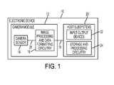
- FIG. 1is a schematic diagram of an electronic device with a camera sensor that may include depth sensing pixels, in accordance with an embodiment of the present invention.
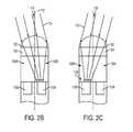
- FIG. 2Ais a cross-sectional view of a pair of depth sensing pixels covered by one microlens that has an asymmetric angular response, in accordance with an embodiment of the present invention.
- FIGS. 2B and 2Care cross-sectional views of a depth sensing pixel that may be asymmetrically sensitive to incident light at negative and positive angles of incidence, in accordance with an embodiment of the present invention.
- FIG. 2Dshows a cross-sectional view and a top view of a pair of depth sensing pixels covered by one microlens, in accordance with an embodiment of the present invention.
- FIG. 3is a diagram of illustrative output signals of a depth sensing pixel for incident light striking the depth sensing pixel at varying angles of incidence, in accordance with an embodiment of the present invention.
- FIG. 4is a diagram of illustrative output signals of depth sensing pixels in a depth sensing pixel pair for incident light striking the depth sensing pixel pair at varying angles of incidence, in accordance with an embodiment of the present invention.
- FIG. 5Ais a diagram of a depth sensing imager having a lens and an object located at a focal distance away from the lens, showing how the lens focuses light from the object onto the depth sensing imager, in accordance with an embodiment of the present invention.
- FIG. 5Bis a diagram of a depth sensing imager having a lens and an object located at more than a focal distance away from the lens, showing how the lens focuses light from the object onto the depth sensing imager, in accordance with an embodiment of the present invention.
- FIG. 5Cis a diagram of a depth sensing imager having a lens and an object located less than a focal distance away from the imaging lens, showing how the lens focuses light from the object onto the depth sensing imager, in accordance with an embodiment of the present invention.
- FIG. 6is a diagram of illustrative depth output signals of a depth sensing pixel pair for an object at varying distances from the depth sensing pixel, in accordance with an embodiment of the present invention.
- FIG. 7is a perspective view of one microlens covering two depth sensing pixels, in accordance with an embodiment of the present invention.
- FIG. 8is a diagram showing a top view of two sets of two depth sensing pixels of FIG. 7 arranged in a Bayer pattern, in accordance with an embodiment of the present invention.
- FIG. 9is diagram of a cross-sectional view of two sets of two depth sensing pixels, showing light entering one light pipe (LP) in each set, in accordance with an embodiment of the present invention.
- FIG. 10is diagram of a side view of the two sets of two depth sensing pixels shown in FIG. 9 .
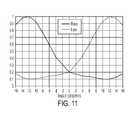
- FIG. 11is plot of the relative signal response versus the incident angle of light entering left and right pixels in each set of pixels shown in FIG. 9 , in accordance with an embodiment of the present invention.
- FIG. 12is a top view of sets of left and right pixels arranged in a Bayer pattern, in accordance with an embodiment of the present invention.
- FIGS. 13A and 13Bare top views of sets of left and right pixels arranged differently so that each forms a Bayer pattern, in accordance with an embodiment of the present invention.
- Electronic device 10may be a digital camera, a computer, a cellular telephone, a medical device, or other electronic device.
- Camera module 12may include image sensor 14 and one or more lenses. During operation, the lenses focus light onto image sensor 14 .
- Image sensor 14includes photosensitive elements (i.e., pixels) that convert the light into digital data. Image sensors may have any number of pixels (e.g., hundreds, thousands, millions, or more).
- image sensor 14may include bias circuitry (e.g., source follower load circuits), sample and hold circuitry, correlated double sampling (CDS) circuitry, amplifier circuitry, analog-to-digital converter (ADC) circuitry, data output circuitry, memory (e.g., buffer circuitry), address circuitry, etc.
- bias circuitrye.g., source follower load circuits
- sample and hold circuitrye.g., sample and hold circuitry
- CDScorrelated double sampling
- ADCanalog-to-digital converter
- data output circuitrye.g., memory (e.g., buffer circuitry), address circuitry, etc.
- Image processing and data formatting circuitry 16may be used to perform image processing functions such as data formatting, adjusting white balance and exposure, implementing video image stabilization, face detection, etc. Image processing and data formatting circuitry 16 may also be used to compress raw camera image files, if desired (e.g., to Joint Photographic Experts Group, or JPEG format). In a typical arrangement, which is sometimes referred to as a system-on-chip, or SOC arrangement, camera sensor 14 and image processing and data formatting circuitry 16 are implemented on a common integrated circuit. The use of a single integrated circuit to implement camera sensor 14 and image processing and data formatting circuitry 16 may help to minimize costs.
- Camera module 12conveys acquired image data to host subsystem 20 over path 18 .
- Electronic device 10typically provides a user with numerous high-level functions. In a computer or advanced cellular telephone, for example, a user may be provided with the ability to run user applications. To implement these functions, host subsystem 20 of electronic device 10 may have input-output devices 22 , such as keypads, input-output ports, joysticks, displays, and storage and processing circuitry 24 .
- Storage and processing circuitry 24may include volatile and nonvolatile memory (e.g., random-access memory, flash memory, hard drives, solid state drives, etc.). Storage and processing circuitry 24 may also include microprocessors, microcontrollers, digital signal processors, application specific integrated circuits, etc.
- camera sensor 14may include pixels such as pixels 100 A, and 100 B, shown in FIG. 2A .
- FIG. 2Ashows an illustrative cross-section of pixels 100 A and 100 B.
- Pixels 100 A and 100 Bmay contain microlens 102 , color filter 104 , a stack of dielectric layers 106 , substrate layer 108 , a photosensitive area, such as photosensitive area 110 A and 110 B formed in substrate layer 108 , and pixel separating areas 112 formed in substrate layer 108 .
- Microlens 102may direct incident light towards a substrate area between pixel separators 112 .
- Color filter 104may filter the incident light by only allowing predetermined wavelengths to pass through color filter 104 (e.g., color filter 104 may only be transparent to wavelengths corresponding to a green color).
- Photosensitive areas 110 A and 110 Bmay serve to absorb incident light focused by microlens 102 and produce image signals that correspond to the amount of incident light absorbed.
- a pair of pixels 100 A and 100 Bmay be covered by one microlens 102 .
- the pair of pixelsmay be provided with an asymmetric angular response (e.g., pixels 100 A and 100 B may produce different image signals based on the angle at which incident light reaches pixels 100 A and 100 B).
- the angle at which incident light reaches pixels 100 A and 100 Bmay be referred to herein as an incident angle, or angle of incidence.
- incident light 113may originate from the left of a normal axis 116 and may reach a pair of pixels 100 A and 100 B with an angle 114 relative to normal axis 116 .
- Angle 114may be a negative angle of incident light.
- Incident light 113 that reaches microlens 102 at a negative angle, such as angle 114may be focused towards photosensitive area 110 A, and pixel 100 A may produce relatively high image signals.
- incident light 113may originate from the right of normal axis 116 and reach the pair of pixels 100 A and 100 B with an angle 118 relative to normal axis 116 .
- Angle 118may be a positive angle of incident light.
- Incident light that reaches microlens 102 at a positive angle, such as angle 118may be focused towards photosensitive area 110 B.
- pixel 100 Bmay produce an image signal output that is relatively high.
- pixels 100 A and 100 Bmay have an asymmetric angular response (e.g., pixel 100 A and 100 B may produce different signal outputs for incident light with a given intensity, based on an angle of incidence).
- pixel 100 A and 100 Bmay produce different signal outputs for incident light with a given intensity, based on an angle of incidence.
- FIG. 3an example of the image output signals of pixel 100 A in response to varying angles of incident light are shown.
- pixel 100 Amay produce larger image signals for negative angles of incident light and smaller image signals for positive angles of incident light. In other words, pixel 100 A produces larger image signals as the incident angle becomes more negative.
- FIG. 2Dillustrates an adjacent pair of pixels ( 100 A and 100 B) with the same microlens, in which pixel 100 A is formed on the right side of the pair, and pixel 100 B is formed on the left side of the pair.
- An adjacent pair of pixels, such as pixels 100 A and 100 B,may be referred to herein as pixel pair 200 .
- the pixel pair 200may also be referred to herein as pixel type 1 and pixel type 2.
- Incident light 113 that reaches pair of pixels 100 A and 100 Bmay have an angle of incidence that is approximately equal for both pixels.
- incident light 113may be focused by microlens 102 A onto photosensitive area 110 B in pixel 100 A and photosensitive area 110 B in pixel 100 B.
- pixel 100 Amay produce an output image signal that is high and pixel 100 B may produce an output image signal that is high by the microlens design.
- the respective output image signals for pixel pair 200are shown in FIG. 4 .
- line 160may reflect the output image signal for pixel 100 A and line 162 may reflect the output image signal for pixel 100 B.
- the output image signal for pixel 100 Amay increase (because incident light is focused onto photosensitive area 110 A of pixel 100 A) and the output image signal for pixel 100 B may decrease (because incident light is focused away from photosensitive area 110 B of pixel 100 B).
- the output image signal for pixel 100 Amay be relatively small and the output image signal for pixel 100 B may be relatively large (e.g., the output signal from pixel 100 A may decrease and the output signal from pixel 100 B may increase).
- Line 164 of FIG. 4may reflect the sum of the output signals for pixel pair 200 . As shown, line 164 may remain relatively constant regardless of the angle of incidence (e.g., for any given angle of incidence, the total amount of light that is absorbed by the combination of pixels 100 A and 100 B may be constant).
- Pixel pairs 200may be used to form imagers with depth sensing capabilities.
- FIGS. 5A, 5B and 5Cshow illustrative image sensors 14 with depth sensing capabilities.
- image sensor 14may contain an array of pixels 201 formed from pixel pairs 200 (e.g., pixel pairs 200 A, 200 B, 200 C, etc.).
- Image sensor 14may have an associated camera lens 202 that focuses light originating from a scene of interest (e.g., a scene that includes an object 204 ) onto the array of pixels.
- Camera lens 202may be located at a distance D F from image sensor 14 .
- Distance D Fmay correspond to the focal length of camera lens 202 .
- object 204may be located at distance D 0 from camera lens 202 .
- Distance D 0may correspond to a focused object plane of camera lens 202 (e.g., a plane located at a distance D 0 from camera lens 202 ).
- the focused object plane and a plane corresponding to image sensor 14may sometimes be referred to as conjugate planes.
- light from object 204may be focused onto pixel pair 200 A, at an angle ⁇ 0 and an angle ⁇ 0 .
- the image output signals of pixels 100 A and 100 B of pixel pair 200may be equal (e.g., most of the light is absorbed by pixel 100 A for the positive angle and most of the light is absorbed by pixel 100 B for the negative angle).
- object 204may be located at a distance D 1 from camera lens 202 .
- Distance D 1may be larger than the distance of the focused object plane (e.g., the focused object plane corresponding to distance D 0 ) of camera lens 202 .
- some of the light from object 204may be focused onto pixel pair 200 B at a negative angle ⁇ 1 (e.g., the light focused by the bottom half pupil of camera lens 202 ) and some of the light from object 204 may be focused onto pixel pair 200 C at a positive angle ⁇ 1 (e.g., the light focused by the top half pupil of camera lens 202 ).
- object 204may be located at a distance D 2 from camera lens 202 .
- Distance D 2may be smaller than the distance of the focused object plane (e.g., the focused object plane corresponding to distance D 0 ) of camera lens 202 .
- some of the light from object 204may be focused by the top half pupil of camera lens 202 onto pixel pair 200 B at a positive angle ⁇ 2 and some of the light from object 204 may be focused by the bottom half pupil of camera lens 202 onto pixel pair 200 C at a negative angle ⁇ 2 .
- FIGS. 5A, 5B and 5Cmay effectively partition the light focused by camera lens 202 into two halves split by a center plane at a midpoint between the top of the lens pupil and the bottom of the lens pupil (e.g., split into a top half and a bottom half).
- Each pixel in the paired pixel array 201may receive different amounts of light from top or bottom half of the lens pupil, respectively. For example, for an object at distance D 1 , pixel 100 A of 200 B may receive more light than pixel 100 B of 200 B. For an object at distance D 2 , pixel 100 A of 200 B may receive less light than 100 B of 200 B.
- the partitioning of the light focused by camera lens 202may be referred to herein as lens partitioning, or lens pupil division.
- the output image signals of each pixel pair 200 of image sensor 14may depend on the distance from camera lens 202 to object 204 .
- the angle at which incident light reaches pixel pairs 200 of image sensor 14depends on the distance between lens 202 and objects in a given scene (e.g., the distance between objects such as object 204 and device 10 ).
- An image depth signalmay be calculated from the difference between the two output image signals of each pixel pair 200 .
- the diagram of FIG. 6shows an image depth signal that may be calculated for pixel pair 200 B by subtracting the image signal output of pixel 100 B from the image signal output of pixel 100 A (e.g., by subtracting line 162 from line 160 of FIG. 4 ).
- the image depth signalmay be negative.
- the image depth signalmay be positive.
- the image depth signalmay remain constant. Pixels 100 A and 100 B may be unable to resolve incident angles with magnitudes larger than the magnitudes of angles provided by objects at distances greater than D 4 , or at distances less than D 3 .
- a depth sensing imagermay be unable to accurately measure depth information for objects at distances greater than D 4 , or at distances less than D 3 .
- the depth sensing imagermay be unable to distinguish whether an object is at a distance D 4 or a distance D 5 (as an example). If desired, the depth sensing imager may assume that all objects that result in an image depth signal equivalent to distance D 2 or D 4 are at a distance of D 2 or D 4 , respectively.
- two dimensional pixel arrays 201may be formed from various combinations of depth sensing pixel pairs 200 and regular pixels (e.g., pixels without asymmetric angular responses).
- regular pixelse.g., pixels without asymmetric angular responses.
- the depth sensing pixelsmay be formed with any desirable types of color filters. Depth sensing pixels may be formed with red color filters, blue color filters, green color filters, or color filters that pass other desirable wavelengths of light, such as infrared and ultraviolet light wavelengths. If desired, depth sensing pixels may be formed with color filters that pass multiple wavelengths of light. For example, to increase the amount of light absorbed by a depth sensing pixel, the depth sensing pixel may be formed with a color filter that passes many wavelengths of light. As another example, the depth sensing pixel may be formed without a color filter (sometimes referred to as a clear pixel).
- the pixel pair 302is similar to the pixel pair 200 shown in FIG. 2D .
- the pixel pairincludes left and right pixels, or as sometimes referred to as pixel type-one and pixel type-two.
- a single microlens 300(same as 102 in FIG. 2D ) is positioned above the left and right pixels so that the single microlens spans across both pixels in the horizontal direction.
- Each pixel pair 302includes a single color filter of a CFA (color filter array) that forms a Bayer pattern.
- Pixel pair 302 Aforms two color filters for green.
- Pixel pair 302 Bforms two color filters for blue.
- Pixel pair 302 Cforms two green filters.
- pixel pairs 302 D, 302 E, 302 F, 302 G and 302 Hform pairs of color filters producing a Bayer pattern.
- FIG. 9there is shown an asymmetric pixel configuration that includes microlens 300 and pixel pair 302 , similar to the pixel configuration of FIG. 7 .
- FIG. 9shows four pixels, namely, pixels 316 A and 316 B forming one pair of pixels on the left side of the figure and pixels 316 A and 316 B forming another pair of pixels on the right side of the figure.
- each microlens 300covers two pixels in the horizontal direction.
- a planarization layer 310is disposed under each microlens 300 .
- a color filterwhich spans across two pixels 316 A and 316 B.
- color filter 312is similar in length to the length of microlens 300 and covers a pixel pair (or a set of pixels).
- each LPDisposed between each color filter 312 and each pixel pair 316 A and 316 B are two light pipes (LPs).
- Each LPimproves the light concentration that impinges upon each respective pixel.
- the LPimproves, not only the light concentration, but also reduces cross-talk and insures good three dimensional performance, even with very small pixel pitches, such as 1.4 microns or less.
- LP 314 BAs shown on the left side of FIG. 9 , light enters pixel photosensitive area 316 B by way of LP 314 B. Similarly, on the right side of FIG. 9 , light enters LP 314 A and pixel photosensitive area 316 A. It will be appreciated that LP 314 B, on the left side of the figure, includes most of the light, because the light passing through microlens 300 is angled at a negative angle with respect to a vertical line through microlens 300 . In a similar way, the light on the right side of the figure, enters LP 314 A, because the light passing through microlens 300 is angled at a positive angle with respect to a vertical line through microlens 300 .
- FIG. 10shows the same pixels as in FIG. 9 , except that a side-view is shown of the pixel pair.
- microlens 300only spans one pixel in the vertical direction, or the column direction of a pixel array. Accordingly, microlens 300 is effective in reducing cross-talk in the vertical direction of the pixel array.
- a side-view of LP 314 and pixel photosensitive area 316is also shown in the figure.
- lightis shown concentrated in LP 314 and passing into pixel photosensitive area 316 .
- FIG. 11shows the relative signal response versus the incident angle of light entering a pixel pair.
- the right pixelor pixel 314 B on the left side of FIG. 9
- the left pixelor pixel 314 A on the right side of FIG. 9
- the pixelalso responds strongly.
- the responses of the left and right pixelsare relatively low. It will be appreciated that if the two pixels forming each pixel pair is summed in the horizontal direction, a normal image may be formed.
- the present inventionobtains depth sensing capabilities.
- the present inventionmay process the color normally for two separate images and obtain two separate Bayer patterns, as shown in FIG. 12 . Accordingly, the two pixel pairs shown on the left side of FIG. 12 may be separated into two images (the left image has two pixels and the right image has two pixels).
- the first pixel pairprovides a green color; when the pair is separated into left and right images, the present invention provides a single green pixel for the left image and a single green pixel for the right image.
- the present inventionforms a left image with a red color and a right image with a red color.
- a 2 ⁇ 1 CFA patternenables the present invention to form a normal Bayer color process for two separate images (left and right Bayer images), as shown in FIG. 12 .
- each arrangementincludes microlenses that cover 2 ⁇ 1 pixels, as shown in FIG. 7 .
- the microlensesare shown zigzag-shifted relative to each other by one pixel in neighboring rows. These arrangement result in no resolution loss in the horizontal direction and would be valuable for HD video format.
- the first and second rows' CFA patternis GRGRGR . . .
- the third and fourth rows' CFA patternsis BGBGBG . . . .
- the 2 ⁇ 1 microlens for the first and third rowsstart from the first column, whereas the microlens for the second and fourth rows start one column earlier, or later. Therefore, the left image pixel array is formed by pixels L1, L2, L3, L4, L5, L6, L7 and L8. Similarly, the right image pixel array is formed by pixels R1, R2, R3, R4, R5, R6, R7 and R8.
- the first and third rowsare an all green CFA
- the second rowis an all red CFA
- the fourth rowis an all blue CFA.
- the 2 ⁇ 1 microlens for the first and third rowsstart from the first column, whereas the microlens for second and fourth rows start one column earlier, or later. Therefore, the left image pixel array is formed by pixels L1, L2, L3, L4, L5, L6, L7 and L8. Similarly, the right image pixel array is formed by pixels R1, R2, R3, R4, R5, R6, R7 and R8.
- each microlenscovers two pixels in the horizontal direction, but only covers one pixel in the vertical direction. Furthermore, the radius of curvature of each microlens in both directions are different due to processing limitations.
- the microlens materialincludes an optical index (n) that varies in range between 1.5 and 1.6.
- the LPmay be filled by material having a higher optical index (n greater than 1.6) than its surrounding oxide material, in which the latter may have an optical index of 1.4 or 1.5. In this manner, the light is maintained within the LP.
Landscapes
- Engineering & Computer Science (AREA)
- Multimedia (AREA)
- Signal Processing (AREA)
- Physics & Mathematics (AREA)
- Spectroscopy & Molecular Physics (AREA)
- Transforming Light Signals Into Electric Signals (AREA)
- Solid State Image Pick-Up Elements (AREA)
Abstract
Description
Claims (19)
Priority Applications (2)
| Application Number | Priority Date | Filing Date | Title |
|---|---|---|---|
| US13/404,319US10015471B2 (en) | 2011-08-12 | 2012-02-24 | Asymmetric angular response pixels for single sensor stereo |
| US15/997,851US20180288398A1 (en) | 2011-08-12 | 2018-06-05 | Asymmetric angular response pixels for singl sensor stereo |
Applications Claiming Priority (2)
| Application Number | Priority Date | Filing Date | Title |
|---|---|---|---|
| US201161522876P | 2011-08-12 | 2011-08-12 | |
| US13/404,319US10015471B2 (en) | 2011-08-12 | 2012-02-24 | Asymmetric angular response pixels for single sensor stereo |
Related Child Applications (1)
| Application Number | Title | Priority Date | Filing Date |
|---|---|---|---|
| US15/997,851ContinuationUS20180288398A1 (en) | 2011-08-12 | 2018-06-05 | Asymmetric angular response pixels for singl sensor stereo |
Publications (2)
| Publication Number | Publication Date |
|---|---|
| US20130038691A1 US20130038691A1 (en) | 2013-02-14 |
| US10015471B2true US10015471B2 (en) | 2018-07-03 |
Family
ID=47677291
Family Applications (2)
| Application Number | Title | Priority Date | Filing Date |
|---|---|---|---|
| US13/404,319Active2034-05-01US10015471B2 (en) | 2011-08-12 | 2012-02-24 | Asymmetric angular response pixels for single sensor stereo |
| US15/997,851AbandonedUS20180288398A1 (en) | 2011-08-12 | 2018-06-05 | Asymmetric angular response pixels for singl sensor stereo |
Family Applications After (1)
| Application Number | Title | Priority Date | Filing Date |
|---|---|---|---|
| US15/997,851AbandonedUS20180288398A1 (en) | 2011-08-12 | 2018-06-05 | Asymmetric angular response pixels for singl sensor stereo |
Country Status (1)
| Country | Link |
|---|---|
| US (2) | US10015471B2 (en) |
Cited By (2)
| Publication number | Priority date | Publication date | Assignee | Title |
|---|---|---|---|---|
| US20180288398A1 (en)* | 2011-08-12 | 2018-10-04 | Semiconductor Components Industries, Llc | Asymmetric angular response pixels for singl sensor stereo |
| US11463677B2 (en)* | 2017-07-13 | 2022-10-04 | Samsung Electronics Co., Ltd. | Image signal processor, image processing system and method of binning pixels in an image sensor |
Families Citing this family (22)
| Publication number | Priority date | Publication date | Assignee | Title |
|---|---|---|---|---|
| JP5631176B2 (en)* | 2010-11-29 | 2014-11-26 | キヤノン株式会社 | Solid-state image sensor and camera |
| US8742309B2 (en) | 2011-01-28 | 2014-06-03 | Aptina Imaging Corporation | Imagers with depth sensing capabilities |
| JP5634613B2 (en)* | 2011-09-28 | 2014-12-03 | 富士フイルム株式会社 | Image sensor and imaging apparatus |
| US9554115B2 (en)* | 2012-02-27 | 2017-01-24 | Semiconductor Components Industries, Llc | Imaging pixels with depth sensing capabilities |
| WO2013136819A1 (en) | 2012-03-16 | 2013-09-19 | 株式会社ニコン | Image sensor, imaging device and imaging system |
| US8922654B2 (en)* | 2012-03-22 | 2014-12-30 | Exelis, Inc. | Algorithm for adaptive downsampling to an irregular grid |
| JP6174940B2 (en)* | 2012-10-19 | 2017-08-02 | キヤノン株式会社 | Imaging device and imaging apparatus |
| JP6120523B2 (en)* | 2012-10-24 | 2017-04-26 | オリンパス株式会社 | Imaging device and imaging apparatus |
| US9445018B2 (en) | 2014-05-01 | 2016-09-13 | Semiconductor Components Industries, Llc | Imaging systems with phase detection pixels |
| US9888198B2 (en) | 2014-06-03 | 2018-02-06 | Semiconductor Components Industries, Llc | Imaging systems having image sensor pixel arrays with sub-pixel resolution capabilities |
| US9338380B2 (en) | 2014-06-30 | 2016-05-10 | Semiconductor Components Industries, Llc | Image processing methods for image sensors with phase detection pixels |
| US9432568B2 (en) | 2014-06-30 | 2016-08-30 | Semiconductor Components Industries, Llc | Pixel arrangements for image sensors with phase detection pixels |
| WO2016051431A1 (en)* | 2014-09-30 | 2016-04-07 | 株式会社ブリリアントサービス | Input/output device, input/output program, and input/output method |
| US9455285B2 (en) | 2015-02-04 | 2016-09-27 | Semiconductors Components Industries, Llc | Image sensors with phase detection pixels |
| US9749556B2 (en) | 2015-03-24 | 2017-08-29 | Semiconductor Components Industries, Llc | Imaging systems having image sensor pixel arrays with phase detection capabilities |
| US9807294B2 (en) | 2015-08-05 | 2017-10-31 | Omnivision Technologies, Inc. | Image sensor with symmetric multi-pixel phase-difference detectors, and associated methods |
| US9936129B2 (en) | 2016-06-15 | 2018-04-03 | Obsidian Sensors, Inc. | Generating high resolution images |
| US10033949B2 (en) | 2016-06-16 | 2018-07-24 | Semiconductor Components Industries, Llc | Imaging systems with high dynamic range and phase detection pixels |
| US10205937B2 (en)* | 2016-08-02 | 2019-02-12 | Apple Inc. | Controlling lens misalignment in an imaging system |
| US10297629B2 (en) | 2017-09-11 | 2019-05-21 | Semiconductor Components Industries, Llc | Image sensors with in-pixel lens arrays |
| US10483309B1 (en) | 2018-09-07 | 2019-11-19 | Semiductor Components Industries, Llc | Image sensors with multipart diffractive lenses |
| US10957727B2 (en) | 2018-09-26 | 2021-03-23 | Semiconductor Components Industries, Llc | Phase detection pixels with diffractive lenses |
Citations (83)
| Publication number | Priority date | Publication date | Assignee | Title |
|---|---|---|---|---|
| US6166768A (en) | 1994-01-28 | 2000-12-26 | California Institute Of Technology | Active pixel sensor array with simple floating gate pixels |
| US6396873B1 (en)* | 1999-02-25 | 2002-05-28 | Envision Advanced Medical Systems | Optical device |
| US20020117605A1 (en)* | 2001-01-08 | 2002-08-29 | Alden Ray M. | Three-dimensional receiving and displaying process and apparatus with military application |
| US20030211405A1 (en) | 2002-05-13 | 2003-11-13 | Kartik Venkataraman | Color filter imaging array and method of formation |
| US20040012698A1 (en)* | 2001-03-05 | 2004-01-22 | Yasuo Suda | Image pickup model and image pickup device |
| US6714240B1 (en)* | 1998-06-23 | 2004-03-30 | Boeing North American, Inc. | Optical sensor employing motion compensated integration-device and process |
| US6856407B2 (en) | 2000-09-13 | 2005-02-15 | Nextengine, Inc. | Method for depth detection in 3D imaging providing a depth measurement for each unitary group of pixels |
| US20050051860A1 (en)* | 2003-09-10 | 2005-03-10 | Fuji Photo Film Co., Ltd. | Solid state image pickup device |
| US20050057655A1 (en) | 2003-09-17 | 2005-03-17 | Kevin Duesman | Method for automated testing of the modulation transfer function in image sensors |
| US6933978B1 (en)* | 1999-10-28 | 2005-08-23 | Canon Kabushiki Kaisha | Focus detecting device with photoelectric conversion portion having microlens and with light blocking portion having first and second openings |
| US20050190453A1 (en)* | 2004-03-01 | 2005-09-01 | Hideki Dobashi | Image sensor |
| US20060066739A1 (en)* | 2004-09-24 | 2006-03-30 | Fuji Photo Film Co., Ltd. | Image pickup apparatus including photosensitive cells each having photosensitive regions partitioned |
| US20060249804A1 (en)* | 2004-07-08 | 2006-11-09 | Chandra Mouli | Photonic crystal-based lens elements for use in an image sensor |
| US20070023801A1 (en) | 2005-07-27 | 2007-02-01 | Magnachip Semiconductor Ltd. | Stacked pixel for high resolution CMOS image sensor |
| US20070090423A1 (en) | 2005-10-25 | 2007-04-26 | Magnachip Semiconductor Ltd. | CMOS image sensor |
| US7290880B1 (en) | 2005-07-27 | 2007-11-06 | Visionsense Ltd. | System and method for producing a stereoscopic image of an eye fundus |
| US20080018662A1 (en) | 2006-07-21 | 2008-01-24 | Gazeley William George | Method and apparatus for preventing or reducing color cross-talk between adjacent pixels in an image sensor device |
| US20080080028A1 (en)* | 2006-10-02 | 2008-04-03 | Micron Technology, Inc. | Imaging method, apparatus and system having extended depth of field |
| US20080180558A1 (en) | 2007-01-16 | 2008-07-31 | Sharp Kabushiki Kaisha | Amplification-type solid-state image capturing apparatus and electronic information device |
| US20080217718A1 (en) | 2007-03-06 | 2008-09-11 | Micron Technology, Inc. | Method, apparatus, and system to reduce ground resistance in a pixel array |
| US20080259202A1 (en)* | 2006-11-28 | 2008-10-23 | Sony Corporation | Imaging device |
| US20080274581A1 (en) | 2007-05-03 | 2008-11-06 | Park Jin-Ho | Method for manufacturing image sensor |
| US20080278820A1 (en)* | 2007-05-08 | 2008-11-13 | Micron Technology, Inc. | Tetraform microlenses and method of forming the same |
| US20090200589A1 (en) | 2008-02-08 | 2009-08-13 | Omnivision Technologies, Inc. | Backside illuminated imaging sensor with improved infrared sensitivity |
| US20090230394A1 (en) | 2008-03-12 | 2009-09-17 | Omnivision Technologies, Inc. | Image sensor array with conformal color filters |
| US20090244514A1 (en)* | 2008-03-26 | 2009-10-01 | Samsung Electronics Co., Ltd. | Distance measuring sensors including vertical photogate and three-dimensional color image sensors including distance measuring sensors |
| US20090284731A1 (en)* | 2008-05-13 | 2009-11-19 | Samsung Electronics Co., Ltd. | Distance measuring sensor including double transfer gate and three dimensional color image sensor including the distance measuring sensor |
| US7646943B1 (en)* | 2008-09-04 | 2010-01-12 | Zena Technologies, Inc. | Optical waveguides in image sensors |
| US20100020209A1 (en) | 2008-07-25 | 2010-01-28 | Samsung Electronics Co., Ltd. | Imaging method and apparatus |
| US20100033829A1 (en)* | 2006-10-10 | 2010-02-11 | Fraunhofer-Gesellschaft zur Förderung der angewandten Forschung e.V. | Device for Homogenizing Radiation by Means of Irregular Microlens Arrays |
| US20100060717A1 (en) | 2006-12-04 | 2010-03-11 | Koninklijke Philips Electronics N.V. | Image processing system for processing combined image data and depth data |
| US20100091161A1 (en)* | 2007-06-16 | 2010-04-15 | Nikon Corporation | Solid-state image sensor and imaging apparatus equipped with solid-state image sensor |
| US20100117177A1 (en) | 2008-11-07 | 2010-05-13 | Young Je Yun | Image Sensor and Method of Manufacturing the Same |
| US20100123771A1 (en) | 2008-11-14 | 2010-05-20 | Samsung Electronics Co., Ltd. | Pixel circuit, photoelectric converter, and image sensing system including the pixel circuit and the photoelectric converter |
| US20100128109A1 (en)* | 2008-11-25 | 2010-05-27 | Banks Paul S | Systems And Methods Of High Resolution Three-Dimensional Imaging |
| US20100150538A1 (en) | 2008-12-15 | 2010-06-17 | Sony Corporation | Image Pickup apparatus and focus control method |
| US20100238330A1 (en)* | 2007-09-13 | 2010-09-23 | Sony Corporation | Solid-state imaging device, signal processing method thereof and image capturing apparatus |
| US20100245656A1 (en)* | 2009-03-31 | 2010-09-30 | Sony Corporation | Imaging device and focus detecting method |
| US20100265381A1 (en)* | 2009-04-16 | 2010-10-21 | Sony Corporation | Imaging device |
| US20100290674A1 (en) | 2009-05-14 | 2010-11-18 | Samsung Electronics Co., Ltd. | 3D image processing apparatus improving depth accuracy of region of interest and method |
| US20110019184A1 (en)* | 2007-10-02 | 2011-01-27 | Nikon Corporation | Light receiving device, focus detection device and imaging device |
| US20110018974A1 (en)* | 2009-07-27 | 2011-01-27 | Sen Wang | Stereoscopic imaging using split complementary color filters |
| US20110019049A1 (en)* | 2009-07-27 | 2011-01-27 | Samsung Electronics Co., Ltd. | Photo detecting apparatus and unit pixel thereof |
| US20110025904A1 (en) | 2008-03-11 | 2011-02-03 | Canon Kabushiki Kaisha | Focus detection device and imaging apparatus having the same |
| US20110042552A1 (en)* | 2009-08-19 | 2011-02-24 | Furuya Shogo | Solid-state imaging device and method of manufacturing the same |
| US7935560B2 (en) | 2007-09-06 | 2011-05-03 | International Business Machines Corporation | Imagers having electrically active optical elements |
| US20110109776A1 (en)* | 2009-11-10 | 2011-05-12 | Fujifilm Corporation | Imaging device and imaging apparatus |
| US20110199602A1 (en)* | 2010-02-17 | 2011-08-18 | Suk Pil Kim | Sensor and method using the same |
| US20110199506A1 (en)* | 2008-11-11 | 2011-08-18 | Canon Kabushiki Kaisha | Focus detection apparatus and control method therefor |
| US20110249161A1 (en) | 2010-04-12 | 2011-10-13 | Canon Kabushiki Kaisha | Solid-state imaging device |
| US8049801B2 (en)* | 2006-09-14 | 2011-11-01 | Nikon Corporation | Image sensor and imaging apparatus |
| US20110309236A1 (en) | 2007-04-18 | 2011-12-22 | Invisage Technologies, Inc. | Materials, systems and methods for optoelectronic devices |
| US20120019695A1 (en) | 2010-07-26 | 2012-01-26 | Omnivision Technologies, Inc. | Image sensor having dark sidewalls between color filters to reduce optical crosstalk |
| US20120043634A1 (en) | 2010-08-17 | 2012-02-23 | Canon Kabushiki Kaisha | Method of manufacturing microlens array, method of manufacturing solid-state image sensor, and solid-state image sensor |
| US20120056073A1 (en)* | 2010-09-03 | 2012-03-08 | Jung Chak Ahn | Pixel, method of manufacturing the same, and image processing devices including the same |
| US20120133809A1 (en)* | 2010-11-29 | 2012-05-31 | Canon Kabushiki Kaisha | Solid state image sensor |
| US20120175501A1 (en) | 2005-09-27 | 2012-07-12 | Omnivision Technologies, Inc. | Image sensing device and manufacture method thereof |
| US20120193515A1 (en)* | 2011-01-28 | 2012-08-02 | Gennadiy Agranov | Imagers with depth sensing capabilities |
| US20120212581A1 (en) | 2011-02-17 | 2012-08-23 | Canon Kabushiki Kaisha | Image capture apparatus and image signal processing apparatus |
| US20120212654A1 (en)* | 2011-02-18 | 2012-08-23 | Canon Kabushiki Kaisha | Image pickup apparatus, focus detection method, image generation method, and storage medium |
| US20120267747A1 (en)* | 2009-12-04 | 2012-10-25 | Canon Kabushiki Kaisha | Solid-state image pickup device and method for manufacturing the same |
| US20120268634A1 (en)* | 2011-04-20 | 2012-10-25 | Canon Kabushiki Kaisha | Image sensor and image capturing apparatus |
| US20130020620A1 (en)* | 2008-09-04 | 2013-01-24 | Zena Technologies, Inc. | Optical waveguides in image sensors |
| US20130038691A1 (en)* | 2011-08-12 | 2013-02-14 | Aptina Imaging Corporation | Asymmetric angular response pixels for single sensor stereo |
| US20130128087A1 (en)* | 2010-08-27 | 2013-05-23 | Todor G. Georgiev | Methods and Apparatus for Super-Resolution in Integral Photography |
| US20130181309A1 (en) | 2012-01-18 | 2013-07-18 | Canon Kabushiki Kaisha | Image pickup apparatus and image pickup system |
| US20130182158A1 (en) | 2012-01-18 | 2013-07-18 | Canon Kabushiki Kaisha | Image pickup apparatus and image pickup system |
| US20130222552A1 (en) | 2012-02-27 | 2013-08-29 | Aptina Imaging Corporation | Imaging pixels with depth sensing capabilities |
| US20130222553A1 (en)* | 2010-09-24 | 2013-08-29 | Fujifilm Corporation | Image pickup device and image pickup apparatus |
| US20130222662A1 (en) | 2012-02-28 | 2013-08-29 | Canon Kabushiki Kaisha | Imaging device, imaging system, and method for driving imaging device |
| US8525906B2 (en)* | 2008-07-18 | 2013-09-03 | Sony Corporation | Solid-state imaging element and camera system |
| US20130256510A1 (en) | 2012-03-29 | 2013-10-03 | Omnivision Technologies, Inc. | Imaging device with floating diffusion switch |
| US20130271646A1 (en) | 2012-04-11 | 2013-10-17 | Canon Kabushiki Kaisha | Image capture apparatus and control method therefor |
| US20140103410A1 (en) | 2012-10-11 | 2014-04-17 | Omnivision Technologies, Inc. | Partial buried channel transfer device in image sensors |
| US8730545B2 (en) | 2011-03-24 | 2014-05-20 | Fujifilm Corporation | Color imaging element, imaging device, and storage medium storing a control program for imaging device |
| US20140192248A1 (en) | 2013-01-07 | 2014-07-10 | Canon Kabushiki Kaisha | Imaging apparatus and method for controlling same |
| US20140218580A1 (en) | 2011-08-26 | 2014-08-07 | E2V Semiconductors | Pixel-grouping image sensor |
| US20140253905A1 (en)* | 2013-03-06 | 2014-09-11 | Samsung Electronics Co., Ltd | Depth pixel and image pick-up apparatus including the same |
| US20150001589A1 (en) | 2013-06-28 | 2015-01-01 | Canon Kabushiki Kaisha | Photoelectric conversion device and imaging system |
| US8947572B2 (en) | 2010-05-24 | 2015-02-03 | Omnivision Technologies, Inc. | Dual-sided image sensor |
| US20150062422A1 (en) | 2013-08-27 | 2015-03-05 | Semiconductor Components Industries, Llc | Lens alignment in camera modules using phase detection pixels |
| US9106826B2 (en) | 2013-09-20 | 2015-08-11 | Fujifilm Corporation | Image capturing apparatus and focusing control method |
| US20150312461A1 (en) | 2014-04-28 | 2015-10-29 | Tae Chan Kim | Image sensor including a pixel having photoelectric conversion elements and image processing device having the image sensor |
Family Cites Families (3)
| Publication number | Priority date | Publication date | Assignee | Title |
|---|---|---|---|---|
| US7321669B2 (en)* | 2003-07-10 | 2008-01-22 | Sarnoff Corporation | Method and apparatus for refining target position and size estimates using image and depth data |
| JP4925354B2 (en)* | 2008-03-31 | 2012-04-25 | 富士フイルム株式会社 | Image processing apparatus, image display apparatus, imaging apparatus, and image processing method |
| JP5293463B2 (en)* | 2009-07-09 | 2013-09-18 | ソニー株式会社 | Image processing apparatus, image processing method, and program |
- 2012
- 2012-02-24USUS13/404,319patent/US10015471B2/enactiveActive
- 2018
- 2018-06-05USUS15/997,851patent/US20180288398A1/ennot_activeAbandoned
Patent Citations (85)
| Publication number | Priority date | Publication date | Assignee | Title |
|---|---|---|---|---|
| US6166768A (en) | 1994-01-28 | 2000-12-26 | California Institute Of Technology | Active pixel sensor array with simple floating gate pixels |
| US6714240B1 (en)* | 1998-06-23 | 2004-03-30 | Boeing North American, Inc. | Optical sensor employing motion compensated integration-device and process |
| US6396873B1 (en)* | 1999-02-25 | 2002-05-28 | Envision Advanced Medical Systems | Optical device |
| US6933978B1 (en)* | 1999-10-28 | 2005-08-23 | Canon Kabushiki Kaisha | Focus detecting device with photoelectric conversion portion having microlens and with light blocking portion having first and second openings |
| US6856407B2 (en) | 2000-09-13 | 2005-02-15 | Nextengine, Inc. | Method for depth detection in 3D imaging providing a depth measurement for each unitary group of pixels |
| US20020117605A1 (en)* | 2001-01-08 | 2002-08-29 | Alden Ray M. | Three-dimensional receiving and displaying process and apparatus with military application |
| US20040012698A1 (en)* | 2001-03-05 | 2004-01-22 | Yasuo Suda | Image pickup model and image pickup device |
| US20030211405A1 (en) | 2002-05-13 | 2003-11-13 | Kartik Venkataraman | Color filter imaging array and method of formation |
| US20050051860A1 (en)* | 2003-09-10 | 2005-03-10 | Fuji Photo Film Co., Ltd. | Solid state image pickup device |
| US20050057655A1 (en) | 2003-09-17 | 2005-03-17 | Kevin Duesman | Method for automated testing of the modulation transfer function in image sensors |
| US20050190453A1 (en)* | 2004-03-01 | 2005-09-01 | Hideki Dobashi | Image sensor |
| US20060249804A1 (en)* | 2004-07-08 | 2006-11-09 | Chandra Mouli | Photonic crystal-based lens elements for use in an image sensor |
| US20060066739A1 (en)* | 2004-09-24 | 2006-03-30 | Fuji Photo Film Co., Ltd. | Image pickup apparatus including photosensitive cells each having photosensitive regions partitioned |
| US20070023801A1 (en) | 2005-07-27 | 2007-02-01 | Magnachip Semiconductor Ltd. | Stacked pixel for high resolution CMOS image sensor |
| US7290880B1 (en) | 2005-07-27 | 2007-11-06 | Visionsense Ltd. | System and method for producing a stereoscopic image of an eye fundus |
| US20120175501A1 (en) | 2005-09-27 | 2012-07-12 | Omnivision Technologies, Inc. | Image sensing device and manufacture method thereof |
| US20070090423A1 (en) | 2005-10-25 | 2007-04-26 | Magnachip Semiconductor Ltd. | CMOS image sensor |
| US20080018662A1 (en) | 2006-07-21 | 2008-01-24 | Gazeley William George | Method and apparatus for preventing or reducing color cross-talk between adjacent pixels in an image sensor device |
| US8049801B2 (en)* | 2006-09-14 | 2011-11-01 | Nikon Corporation | Image sensor and imaging apparatus |
| US20080080028A1 (en)* | 2006-10-02 | 2008-04-03 | Micron Technology, Inc. | Imaging method, apparatus and system having extended depth of field |
| US20100033829A1 (en)* | 2006-10-10 | 2010-02-11 | Fraunhofer-Gesellschaft zur Förderung der angewandten Forschung e.V. | Device for Homogenizing Radiation by Means of Irregular Microlens Arrays |
| US20080259202A1 (en)* | 2006-11-28 | 2008-10-23 | Sony Corporation | Imaging device |
| US20100060717A1 (en) | 2006-12-04 | 2010-03-11 | Koninklijke Philips Electronics N.V. | Image processing system for processing combined image data and depth data |
| US20080180558A1 (en) | 2007-01-16 | 2008-07-31 | Sharp Kabushiki Kaisha | Amplification-type solid-state image capturing apparatus and electronic information device |
| US20080217718A1 (en) | 2007-03-06 | 2008-09-11 | Micron Technology, Inc. | Method, apparatus, and system to reduce ground resistance in a pixel array |
| US20110309236A1 (en) | 2007-04-18 | 2011-12-22 | Invisage Technologies, Inc. | Materials, systems and methods for optoelectronic devices |
| US20080274581A1 (en) | 2007-05-03 | 2008-11-06 | Park Jin-Ho | Method for manufacturing image sensor |
| US20080278820A1 (en)* | 2007-05-08 | 2008-11-13 | Micron Technology, Inc. | Tetraform microlenses and method of forming the same |
| US20100091161A1 (en)* | 2007-06-16 | 2010-04-15 | Nikon Corporation | Solid-state image sensor and imaging apparatus equipped with solid-state image sensor |
| US7935560B2 (en) | 2007-09-06 | 2011-05-03 | International Business Machines Corporation | Imagers having electrically active optical elements |
| US20100238330A1 (en)* | 2007-09-13 | 2010-09-23 | Sony Corporation | Solid-state imaging device, signal processing method thereof and image capturing apparatus |
| US20110019184A1 (en)* | 2007-10-02 | 2011-01-27 | Nikon Corporation | Light receiving device, focus detection device and imaging device |
| US20090200589A1 (en) | 2008-02-08 | 2009-08-13 | Omnivision Technologies, Inc. | Backside illuminated imaging sensor with improved infrared sensitivity |
| US20110025904A1 (en) | 2008-03-11 | 2011-02-03 | Canon Kabushiki Kaisha | Focus detection device and imaging apparatus having the same |
| US20090230394A1 (en) | 2008-03-12 | 2009-09-17 | Omnivision Technologies, Inc. | Image sensor array with conformal color filters |
| US20090244514A1 (en)* | 2008-03-26 | 2009-10-01 | Samsung Electronics Co., Ltd. | Distance measuring sensors including vertical photogate and three-dimensional color image sensors including distance measuring sensors |
| US20090284731A1 (en)* | 2008-05-13 | 2009-11-19 | Samsung Electronics Co., Ltd. | Distance measuring sensor including double transfer gate and three dimensional color image sensor including the distance measuring sensor |
| US8525906B2 (en)* | 2008-07-18 | 2013-09-03 | Sony Corporation | Solid-state imaging element and camera system |
| US20100020209A1 (en) | 2008-07-25 | 2010-01-28 | Samsung Electronics Co., Ltd. | Imaging method and apparatus |
| US20130020620A1 (en)* | 2008-09-04 | 2013-01-24 | Zena Technologies, Inc. | Optical waveguides in image sensors |
| US7646943B1 (en)* | 2008-09-04 | 2010-01-12 | Zena Technologies, Inc. | Optical waveguides in image sensors |
| US20100117177A1 (en) | 2008-11-07 | 2010-05-13 | Young Je Yun | Image Sensor and Method of Manufacturing the Same |
| US20110199506A1 (en)* | 2008-11-11 | 2011-08-18 | Canon Kabushiki Kaisha | Focus detection apparatus and control method therefor |
| US20100123771A1 (en) | 2008-11-14 | 2010-05-20 | Samsung Electronics Co., Ltd. | Pixel circuit, photoelectric converter, and image sensing system including the pixel circuit and the photoelectric converter |
| US20100128109A1 (en)* | 2008-11-25 | 2010-05-27 | Banks Paul S | Systems And Methods Of High Resolution Three-Dimensional Imaging |
| US20100150538A1 (en) | 2008-12-15 | 2010-06-17 | Sony Corporation | Image Pickup apparatus and focus control method |
| US20100245656A1 (en)* | 2009-03-31 | 2010-09-30 | Sony Corporation | Imaging device and focus detecting method |
| US20100265381A1 (en)* | 2009-04-16 | 2010-10-21 | Sony Corporation | Imaging device |
| US20100290674A1 (en) | 2009-05-14 | 2010-11-18 | Samsung Electronics Co., Ltd. | 3D image processing apparatus improving depth accuracy of region of interest and method |
| US20110018974A1 (en)* | 2009-07-27 | 2011-01-27 | Sen Wang | Stereoscopic imaging using split complementary color filters |
| US20110019049A1 (en)* | 2009-07-27 | 2011-01-27 | Samsung Electronics Co., Ltd. | Photo detecting apparatus and unit pixel thereof |
| US20110042552A1 (en)* | 2009-08-19 | 2011-02-24 | Furuya Shogo | Solid-state imaging device and method of manufacturing the same |
| US20110109776A1 (en)* | 2009-11-10 | 2011-05-12 | Fujifilm Corporation | Imaging device and imaging apparatus |
| US20120267747A1 (en)* | 2009-12-04 | 2012-10-25 | Canon Kabushiki Kaisha | Solid-state image pickup device and method for manufacturing the same |
| US20110199602A1 (en)* | 2010-02-17 | 2011-08-18 | Suk Pil Kim | Sensor and method using the same |
| US20110249161A1 (en) | 2010-04-12 | 2011-10-13 | Canon Kabushiki Kaisha | Solid-state imaging device |
| US8947572B2 (en) | 2010-05-24 | 2015-02-03 | Omnivision Technologies, Inc. | Dual-sided image sensor |
| US20120019695A1 (en) | 2010-07-26 | 2012-01-26 | Omnivision Technologies, Inc. | Image sensor having dark sidewalls between color filters to reduce optical crosstalk |
| US20120043634A1 (en) | 2010-08-17 | 2012-02-23 | Canon Kabushiki Kaisha | Method of manufacturing microlens array, method of manufacturing solid-state image sensor, and solid-state image sensor |
| US20130128087A1 (en)* | 2010-08-27 | 2013-05-23 | Todor G. Georgiev | Methods and Apparatus for Super-Resolution in Integral Photography |
| US20120056073A1 (en)* | 2010-09-03 | 2012-03-08 | Jung Chak Ahn | Pixel, method of manufacturing the same, and image processing devices including the same |
| US20130222553A1 (en)* | 2010-09-24 | 2013-08-29 | Fujifilm Corporation | Image pickup device and image pickup apparatus |
| US20120133809A1 (en)* | 2010-11-29 | 2012-05-31 | Canon Kabushiki Kaisha | Solid state image sensor |
| US20160099273A1 (en) | 2011-01-28 | 2016-04-07 | Semiconductor Components Industries, Llc | Imagers with depth sensing capabilities |
| US20120193515A1 (en)* | 2011-01-28 | 2012-08-02 | Gennadiy Agranov | Imagers with depth sensing capabilities |
| US20120212581A1 (en) | 2011-02-17 | 2012-08-23 | Canon Kabushiki Kaisha | Image capture apparatus and image signal processing apparatus |
| US20120212654A1 (en)* | 2011-02-18 | 2012-08-23 | Canon Kabushiki Kaisha | Image pickup apparatus, focus detection method, image generation method, and storage medium |
| US8730545B2 (en) | 2011-03-24 | 2014-05-20 | Fujifilm Corporation | Color imaging element, imaging device, and storage medium storing a control program for imaging device |
| US20120268634A1 (en)* | 2011-04-20 | 2012-10-25 | Canon Kabushiki Kaisha | Image sensor and image capturing apparatus |
| US20130038691A1 (en)* | 2011-08-12 | 2013-02-14 | Aptina Imaging Corporation | Asymmetric angular response pixels for single sensor stereo |
| US20140218580A1 (en) | 2011-08-26 | 2014-08-07 | E2V Semiconductors | Pixel-grouping image sensor |
| US20130182158A1 (en) | 2012-01-18 | 2013-07-18 | Canon Kabushiki Kaisha | Image pickup apparatus and image pickup system |
| US20130181309A1 (en) | 2012-01-18 | 2013-07-18 | Canon Kabushiki Kaisha | Image pickup apparatus and image pickup system |
| US20130222552A1 (en) | 2012-02-27 | 2013-08-29 | Aptina Imaging Corporation | Imaging pixels with depth sensing capabilities |
| US20170094260A1 (en) | 2012-02-27 | 2017-03-30 | Semiconductor Components Industries, Llc | Imaging pixels with depth sensing capabilities |
| US20130222662A1 (en) | 2012-02-28 | 2013-08-29 | Canon Kabushiki Kaisha | Imaging device, imaging system, and method for driving imaging device |
| US20130256510A1 (en) | 2012-03-29 | 2013-10-03 | Omnivision Technologies, Inc. | Imaging device with floating diffusion switch |
| US20130271646A1 (en) | 2012-04-11 | 2013-10-17 | Canon Kabushiki Kaisha | Image capture apparatus and control method therefor |
| US20140103410A1 (en) | 2012-10-11 | 2014-04-17 | Omnivision Technologies, Inc. | Partial buried channel transfer device in image sensors |
| US20140192248A1 (en) | 2013-01-07 | 2014-07-10 | Canon Kabushiki Kaisha | Imaging apparatus and method for controlling same |
| US20140253905A1 (en)* | 2013-03-06 | 2014-09-11 | Samsung Electronics Co., Ltd | Depth pixel and image pick-up apparatus including the same |
| US20150001589A1 (en) | 2013-06-28 | 2015-01-01 | Canon Kabushiki Kaisha | Photoelectric conversion device and imaging system |
| US20150062422A1 (en) | 2013-08-27 | 2015-03-05 | Semiconductor Components Industries, Llc | Lens alignment in camera modules using phase detection pixels |
| US9106826B2 (en) | 2013-09-20 | 2015-08-11 | Fujifilm Corporation | Image capturing apparatus and focusing control method |
| US20150312461A1 (en) | 2014-04-28 | 2015-10-29 | Tae Chan Kim | Image sensor including a pixel having photoelectric conversion elements and image processing device having the image sensor |
Non-Patent Citations (2)
| Title |
|---|
| "An Objective Look at FSI and BSI", An Aptina Technology White Paper, 2010 (6 pages) [Retrieved on Jun. 18, 2012], Retrieved from the Internet <URL: http://www.aptina.com/news/FSI-BSI-WhitePaper.pdf>. |
| Adelson and Wang, "Single Lens Stereo with a Plenoptic Camera", IEEE PAMI, vol. 14, No. 2, (Feb. 1992). |
Cited By (5)
| Publication number | Priority date | Publication date | Assignee | Title |
|---|---|---|---|---|
| US20180288398A1 (en)* | 2011-08-12 | 2018-10-04 | Semiconductor Components Industries, Llc | Asymmetric angular response pixels for singl sensor stereo |
| US11463677B2 (en)* | 2017-07-13 | 2022-10-04 | Samsung Electronics Co., Ltd. | Image signal processor, image processing system and method of binning pixels in an image sensor |
| US20230019882A1 (en)* | 2017-07-13 | 2023-01-19 | Samsung Electronics Co., Ltd. | Image signal processor, image processing system and method of binning pixels in image sensor |
| US11956411B2 (en)* | 2017-07-13 | 2024-04-09 | Samsung Electronics Co., Ltd. | Image signal processor, image processing system and method of binning pixels in image sensor |
| US20240283904A1 (en)* | 2017-07-13 | 2024-08-22 | Samsung Electronics Co., Ltd. | Image signal processor, image processing system and method of binning pixels in image sensor |
Also Published As
| Publication number | Publication date |
|---|---|
| US20180288398A1 (en) | 2018-10-04 |
| US20130038691A1 (en) | 2013-02-14 |
Similar Documents
| Publication | Publication Date | Title |
|---|---|---|
| US10015471B2 (en) | Asymmetric angular response pixels for single sensor stereo | |
| US10014336B2 (en) | Imagers with depth sensing capabilities | |
| US10015416B2 (en) | Imaging systems with high dynamic range and phase detection pixels | |
| US10498990B2 (en) | Imaging systems with high dynamic range and phase detection pixels | |
| US10158843B2 (en) | Imaging pixels with depth sensing capabilities | |
| US9881951B2 (en) | Image sensors with phase detection pixels | |
| CN206759600U (en) | Imaging system | |
| CN211404505U (en) | Image sensor with a plurality of pixels | |
| US9883128B2 (en) | Imaging systems with high dynamic range and phase detection pixels | |
| JP5538553B2 (en) | Solid-state imaging device and imaging apparatus | |
| US10593712B2 (en) | Image sensors with high dynamic range and infrared imaging toroidal pixels | |
| US9432568B2 (en) | Pixel arrangements for image sensors with phase detection pixels | |
| US10419664B2 (en) | Image sensors with phase detection pixels and a variable aperture | |
| CN206727072U (en) | Imaging system with global shutter phase-detection pixel | |
| US20180301484A1 (en) | Image sensors with high dynamic range and autofocusing hexagonal pixels | |
| CN110957336B (en) | Phase detection pixel with diffraction lens | |
| JP2012211942A (en) | Solid-state image sensor and image pickup apparatus |
Legal Events
| Date | Code | Title | Description |
|---|---|---|---|
| AS | Assignment | Owner name:APTINA IMAGING CORPORATION, CAYMAN ISLANDS Free format text:ASSIGNMENT OF ASSIGNORS INTEREST;ASSIGNORS:AGRANOV, GENNADIY;CAO, DONGQING;YARON, AVI;REEL/FRAME:027758/0566 Effective date:20120223 | |
| AS | Assignment | Owner name:SEMICONDUCTOR COMPONENTS INDUSTRIES, LLC, ARIZONA Free format text:ASSIGNMENT OF ASSIGNORS INTEREST;ASSIGNOR:APTINA IMAGING CORPORATION;REEL/FRAME:034673/0001 Effective date:20141217 | |
| AS | Assignment | Owner name:DEUTSCHE BANK AG NEW YORK BRANCH, NEW YORK Free format text:SECURITY INTEREST;ASSIGNOR:SEMICONDUCTOR COMPONENTS INDUSTRIES, LLC;REEL/FRAME:038620/0087 Effective date:20160415 | |
| AS | Assignment | Owner name:DEUTSCHE BANK AG NEW YORK BRANCH, AS COLLATERAL AG Free format text:CORRECTIVE ASSIGNMENT TO CORRECT THE INCORRECT PATENT NUMBER 5859768 AND TO RECITE COLLATERAL AGENT ROLE OF RECEIVING PARTY IN THE SECURITY INTEREST PREVIOUSLY RECORDED ON REEL 038620 FRAME 0087. ASSIGNOR(S) HEREBY CONFIRMS THE SECURITY INTEREST;ASSIGNOR:SEMICONDUCTOR COMPONENTS INDUSTRIES, LLC;REEL/FRAME:039853/0001 Effective date:20160415 Owner name:DEUTSCHE BANK AG NEW YORK BRANCH, AS COLLATERAL AGENT, NEW YORK Free format text:CORRECTIVE ASSIGNMENT TO CORRECT THE INCORRECT PATENT NUMBER 5859768 AND TO RECITE COLLATERAL AGENT ROLE OF RECEIVING PARTY IN THE SECURITY INTEREST PREVIOUSLY RECORDED ON REEL 038620 FRAME 0087. ASSIGNOR(S) HEREBY CONFIRMS THE SECURITY INTEREST;ASSIGNOR:SEMICONDUCTOR COMPONENTS INDUSTRIES, LLC;REEL/FRAME:039853/0001 Effective date:20160415 | |
| STCF | Information on status: patent grant | Free format text:PATENTED CASE | |
| MAFP | Maintenance fee payment | Free format text:PAYMENT OF MAINTENANCE FEE, 4TH YEAR, LARGE ENTITY (ORIGINAL EVENT CODE: M1551); ENTITY STATUS OF PATENT OWNER: LARGE ENTITY Year of fee payment:4 | |
| AS | Assignment | Owner name:FAIRCHILD SEMICONDUCTOR CORPORATION, ARIZONA Free format text:RELEASE OF SECURITY INTEREST IN PATENTS RECORDED AT REEL 038620, FRAME 0087;ASSIGNOR:DEUTSCHE BANK AG NEW YORK BRANCH, AS COLLATERAL AGENT;REEL/FRAME:064070/0001 Effective date:20230622 Owner name:SEMICONDUCTOR COMPONENTS INDUSTRIES, LLC, ARIZONA Free format text:RELEASE OF SECURITY INTEREST IN PATENTS RECORDED AT REEL 038620, FRAME 0087;ASSIGNOR:DEUTSCHE BANK AG NEW YORK BRANCH, AS COLLATERAL AGENT;REEL/FRAME:064070/0001 Effective date:20230622 |