US10008637B2 - Light emitter devices and methods with reduced dimensions and improved light output - Google Patents
Light emitter devices and methods with reduced dimensions and improved light outputDownload PDFInfo
- Publication number
- US10008637B2 US10008637B2US13/312,518US201113312518AUS10008637B2US 10008637 B2US10008637 B2US 10008637B2US 201113312518 AUS201113312518 AUS 201113312518AUS 10008637 B2US10008637 B2US 10008637B2
- Authority
- US
- United States
- Prior art keywords
- submount
- lens
- light emitter
- light
- emitting chip
- Prior art date
- Legal status (The legal status is an assumption and is not a legal conclusion. Google has not performed a legal analysis and makes no representation as to the accuracy of the status listed.)
- Active, expires
Links
Images


Classifications
- H—ELECTRICITY
- H10—SEMICONDUCTOR DEVICES; ELECTRIC SOLID-STATE DEVICES NOT OTHERWISE PROVIDED FOR
- H10H—INORGANIC LIGHT-EMITTING SEMICONDUCTOR DEVICES HAVING POTENTIAL BARRIERS
- H10H20/00—Individual inorganic light-emitting semiconductor devices having potential barriers, e.g. light-emitting diodes [LED]
- H10H20/80—Constructional details
- H10H20/85—Packages
- H10H20/8506—Containers
- H—ELECTRICITY
- H10—SEMICONDUCTOR DEVICES; ELECTRIC SOLID-STATE DEVICES NOT OTHERWISE PROVIDED FOR
- H10H—INORGANIC LIGHT-EMITTING SEMICONDUCTOR DEVICES HAVING POTENTIAL BARRIERS
- H10H20/00—Individual inorganic light-emitting semiconductor devices having potential barriers, e.g. light-emitting diodes [LED]
- H10H20/80—Constructional details
- H10H20/85—Packages
- H10H20/855—Optical field-shaping means, e.g. lenses
- H01L33/486—
- H01L33/54—
- H01L33/58—
- H—ELECTRICITY
- H10—SEMICONDUCTOR DEVICES; ELECTRIC SOLID-STATE DEVICES NOT OTHERWISE PROVIDED FOR
- H10H—INORGANIC LIGHT-EMITTING SEMICONDUCTOR DEVICES HAVING POTENTIAL BARRIERS
- H10H20/00—Individual inorganic light-emitting semiconductor devices having potential barriers, e.g. light-emitting diodes [LED]
- H10H20/80—Constructional details
- H10H20/81—Bodies
- H10H20/819—Bodies characterised by their shape, e.g. curved or truncated substrates
- H—ELECTRICITY
- H10—SEMICONDUCTOR DEVICES; ELECTRIC SOLID-STATE DEVICES NOT OTHERWISE PROVIDED FOR
- H10H—INORGANIC LIGHT-EMITTING SEMICONDUCTOR DEVICES HAVING POTENTIAL BARRIERS
- H10H20/00—Individual inorganic light-emitting semiconductor devices having potential barriers, e.g. light-emitting diodes [LED]
- H10H20/80—Constructional details
- H10H20/85—Packages
- H10H20/852—Encapsulations
- H10H20/853—Encapsulations characterised by their shape
- H—ELECTRICITY
- H01—ELECTRIC ELEMENTS
- H01L—SEMICONDUCTOR DEVICES NOT COVERED BY CLASS H10
- H01L2924/00—Indexing scheme for arrangements or methods for connecting or disconnecting semiconductor or solid-state bodies as covered by H01L24/00
- H—ELECTRICITY
- H01—ELECTRIC ELEMENTS
- H01L—SEMICONDUCTOR DEVICES NOT COVERED BY CLASS H10
- H01L2924/00—Indexing scheme for arrangements or methods for connecting or disconnecting semiconductor or solid-state bodies as covered by H01L24/00
- H01L2924/0001—Technical content checked by a classifier
- H01L2924/0002—Not covered by any one of groups H01L24/00, H01L24/00 and H01L2224/00
- H01L33/20—
Definitions
- the subject matter hereinrelates generally to light emitter devices and methods. More particularly, the subject matter herein relates to improved light emitter devices and methods with reduced dimensions and improved light output.
- LEDsLight emitting diodes
- LEDscan be utilized in light emitter devices or packages for providing different color points of light, for example, blue, red, and green light, combinations of light having different color points, and white light (e.g., perceived as being white or near-white).
- Light emitter devices or packagesare developing as replacements for incandescent, fluorescent, and metal halide high-intensity discharge (HID) light products.
- Conventional devicesmay utilize optical elements such as lenses for improving the amount of light extracted from such devices.
- optical elementssuch as lenses for improving the amount of light extracted from such devices.
- One problem with conventional lensesis that various dimensions or ratios such as a lens to submount ratio, edge exclusion, and other dimensions are not fully reduced and/or improved for light extraction. This is because in one aspect, conventional lenses fail to extend near or proximate the edges of the submount.
- FIG. 1is a top perspective view of one embodiment of a light emitter device according to the disclosure herein;
- FIG. 2is another top perspective view of the light emitter device of FIG. 1 ;
- FIGS. 3A and 3Bare top plan views of the light emitter device of FIG. 1 ;
- FIG. 4is a side view of the light emitter device of FIG. 1 ;
- FIG. 5is a bottom plan view of the light emitter device of FIG. 1 ;
- FIGS. 6A to 6Care a top view, a cross-section, and a bottom view, respectively, of a light emitting chip according to the disclosure herein;
- FIGS. 7 and 8illustrate various geometries associated with light emitting chips according to the subject matter herein.
- references to a structure being formed “on” or “above” another structure or portioncontemplates that additional structure, portion, or both may intervene. References to a structure or a portion being formed “on” another structure or portion without an intervening structure or portion are described herein as being formed “directly on” the structure or portion.
- relative terms such as “on”, “above”, “upper”, “top”, “lower”, or “bottom”are used herein to describe one structure's or portion's relationship to another structure or portion as illustrated in the figures. It will be understood that relative terms such as “on”, “above”, “upper”, “top”, “lower” or “bottom” are intended to encompass different orientations of the device in addition to the orientation depicted in the figures. For example, if the device in the figures is turned over, structure or portion described as “above” other structures or portions would now be oriented “below” the other structures or portions. Likewise, if devices in the figures are rotated along an axis, structure or portion described as “above”, other structures or portions would now be oriented “next to” or “left of” the other structures or portions. Like numbers refer to like elements throughout.
- Light emitting devicescan comprise group III-V nitride (e.g., gallium nitride (GaN)) based light emitting diodes (LEDs) or lasers that can be fabricated on a growth substrate, for example, a silicon carbide (SiC) substrate, such as those devices manufactured and sold by Cree, Inc. of Durham, N.C.
- a silicon carbide (SiC) substratesuch as those devices manufactured and sold by Cree, Inc. of Durham, N.C.
- Other growth substratesare also contemplated herein, for example and not limited to sapphire, silicon (Si) and GaN.
- SiC substrates/layerscan be 4H polytype silicon carbide substrates/layers.
- Other Sic candidate polytypes, such as 3C, 6H, and 15R polytypes, however,can be used.
- SiC substratesare available from Cree, Inc., of Durham, N.C., the assignee of the present subject matter, and the methods for producing such substrates are set forth in the scientific literature as well as in a number of commonly assigned U.S. patents, including but not limited to U.S. Pat. No. Re. 34,861; U.S. Pat. No. 4,946,547; and U.S. Pat. No. 5,200,022, the disclosures of which are incorporated by reference herein in their entireties. Any other suitable growth substrates are contemplated herein.
- Group III nitriderefers to those semiconducting compounds formed between nitrogen and one or more elements in Group III of the periodic table, usually aluminum (Al), gallium (Ga), and indium (In).
- the termalso refers to binary, ternary, and quaternary compounds such as GaN, AlGaN and AlInGaN.
- the Group III elementscan combine with nitrogen to form binary (e.g., GaN), ternary (e.g., AlGaN), and quaternary (e.g., AlInGaN) compounds. These compounds may have empirical formulas in which one mole of nitrogen is combined with a total of one mole of the Group III elements. Accordingly, formulas such as AlxGaxN where 1>x>0 are often used to describe these compounds. Techniques for epitaxial growth of Group III nitrides have become reasonably well developed and reported in the appropriate scientific literature.
- LEDs disclosed hereincomprise a growth substrate
- the crystalline epitaxial growth substrate on which the epitaxial layers comprising an LED are growncan be removed, and the freestanding epitaxial layers can be mounted on a substitute carrier substrate or substrate which can have different thermal, electrical, structural and/or optical characteristics than the original substrate.
- the subject matter described hereinis not limited to structures having crystalline epitaxial growth substrates and can be used in connection with structures in which the epitaxial layers have been removed from their original growth substrates and bonded to substitute carrier substrates.
- Group III nitride based LEDscan be fabricated on growth substrates (e.g., Si, SiC, or sapphire substrates) to provide horizontal devices (with at least two electrical contacts on a same side of the LED) or vertical devices (with electrical contacts on opposing sides of the LED).
- the growth substratecan be maintained on the LED after fabrication or removed (e.g., by etching, grinding, polishing, etc.). The growth substrate can be removed, for example, to reduce a thickness of the resulting LED and/or to reduce a forward voltage through a vertical LED.
- a horizontal device(with or without the growth substrate), for example, can be flip chip bonded (e.g., using solder) to a carrier substrate or printed circuit board (PCB), or wire bonded.
- a vertical device(with or without the growth substrate) can have a first terminal solder bonded to a carrier substrate, mounting area, or PCB and a second terminal wire bonded to the carrier substrate, electrical element, or PCB. Examples of vertical and horizontal LED chip structures are discussed by way of example in U.S. Publication No. 2008/0258130 to Bergmann et al. and in U.S. Publication No. 2006/0186418 to Edmond et al., the disclosures of which are hereby incorporated by reference herein in their entireties.
- one or more LED chipscan be at least partially coated with one or more phosphors.
- the phosphorscan absorb a portion of the LED light and emit a different wavelength of light such that the light emitter device or package emits a combination of light from each of the LED and the phosphor.
- the emitter device or packageemits what is perceived as white light resulting from a combination of light emission from the LED chip and the phosphor.
- One or more LEDscan be coated and fabricated using many different methods, with one suitable method being described in U.S. patent application Ser. Nos.
- LEDscan also be coated using other methods such electrophoretic deposition (EPD), with a suitable EPD method described in U.S. patent application Ser. No. 11/473,089 entitled “Close Loop Electrophoretic Deposition of Semiconductor Devices”, which is also incorporated herein by reference in its entirety. It is understood that light emitter devices and methods according to the present subject matter can also have multiple LEDs of different colors, one or more of which can be white emitting.
- EPDelectrophoretic deposition
- FIGS. 1 to 5illustrate one configuration or embodiment of a light emitter type, or LED, package or device, generally designated 10 , according to the present subject matter.
- FIGS. 6A to 8illustrate various embodiments of LED chips that can be incorporated into the novel light emitter packages and devices disclosed herein.
- devices and chips described hereincan be dimensionally reduced and improved in various dimensional aspects for providing improved light extraction and to achieve the best possible performance relative to dimensional aspects of the device, such as for example the size of the device.
- light emitter devices described hereincan be operable to emit light at approximately 100 lumens or higher, or any sub-ranges of that, such as 100 to 150 lumens, 150 to 200 lumens, or more than 200 lumens.
- a light emitter in accordance with the subject matter hereinis operable to emit light with an output of approximately 110 lumens per watt or higher when driven at 350 milliamps (mA).
- devices described hereincan be operable is up to and including 1 amp (A). These luminous efficacies can, for example, be under conditions such as 25° C. (77° F.).
- Light emitter device 10can comprise various features disposed under a lens 30 , which, as illustrated, can comprise a substantially circular lens base B.
- lens 30appears in broken lines, as lens 30 may be optically opaque as illustrated by FIG. 2 .
- the broken lines in FIG. 1are for illustration purposes only and denote placement of lens 30 relative to features which may be disposed below lens 30 as such features may not be seen beneath an opaque lens 30 (e.g., see FIG. 2 ).
- light emitter device 10can comprise at least one light emitter such as a solid state emitter or LED chip 12 that can be disposed or arranged over a chip or die attach area referred to herein as a mounting area, generally designated 14 .
- Mounting area 14can comprise patterned conductive features for passing electrical current into LED chip 12 as well as providing an area for laterally spreading heat.
- LED chip 12 as shown in FIG. 1is for illustration purposes only as LED chip can be of any suitable shape or configuration, see for example, FIGS. 6A to 8 describing various feature and/or embodiments of LED chip 12 .
- LED chip 12can comprise any of the embodiments depicted by FIGS. 6A to 8 as described further herein.
- Mounting area 14can comprise any suitable electrically conductive material known in the art, for example, metals or metal alloys, copper (Cu), aluminum (Al), tin (Sn), silver (Ag), conductive polymer material(s), and/or combinations thereof.
- Mounting area 14can be formed integrally with or electrically and/or thermally isolated from electrical components of light emitter device 10 .
- electrical componentscan comprise first and second electrical contact areas or elements 16 and 18 , respectively.
- First and second electrical elements 16 and 18can comprise, for example and without limitation, any suitable electrically conducting material known in the art, for example, metals or metal alloys, Cu, Al, Sn, Ag, conductive polymer material(s), and/or combinations thereof.
- mounting area 14 and first and second electrical elements 16 and 18can comprise copper (Cu) deposited using known techniques such as plating.
- a titanium adhesion layer and copper seed layercan be sequentially sputtered onto submount 22 . Then, approximately 75 ⁇ m of Cu can be plated onto the Cu seed layer. The resulting Cu layer being deposited can then be patterned using standard lithographic processes.
- the Cu layercan be sputtered using a mask to form the desired pattern of elements 16 and 18 such that the mask is used to form a gap, generally designated G, by preventing deposition of Cu in that area.
- mounting area 14 and elements 16 and 18can be plated or coated with additional metals or materials to the make mounting area 14 more suitable for mounting LED chip 12 and/or to improve optical properties, such as amount of light emitted by device 10 .
- the mounting area 14 and elements 16 and 18can be plated with adhesive materials, bonding materials, reflective materials, and/or barrier materials or layers.
- mounting area 14 and elements 16 and 18can be plated with any suitable thickness of a nickel (Ni) barrier layer and a reflective Ag layer disposed over the Ni barrier layer for increasing reflection from device 10 .
- mounting area 14 and first and second electrical elements 16 and 18can be disposed over and/or attached to a top surface 20 of a substrate or submount 22 .
- mounting area 14can be integrally formed with and as an extension of first and/or second electrical elements 16 or 18 , respectively.
- First electrical element 16 and second electrical element 18can be physically separated and electrically and/or thermally isolated from each other such as by gap G.
- Gap Gcan extend down to top surface 20 of submount 22 thereby electrically and thermally isolating electrical elements 16 and 18 .
- gap Gcan provide electrical isolation between the first and second electrical elements 16 and 18 to prevent shorting of the electrical signal applied to LED chip 12 .
- mounting area 14 and electrical elements 16 and 18can provide laterally extending thermally conductive paths for conducting heat away from LED chip 12 such that it can spread to other areas of submount 22 beyond areas just below LED chip 12 .
- mounting area 14can cover more surface area of top surface 20 of submount 22 than that covered by LED chip 12 .
- Mounting area 14can extend proximate or to the edges of submount 22 . In the embodiment shown, mounting area 14 is generally circular and extends radially from LED chip 12 toward the edges of submount 22 . It is understood that mounting area 14 can comprise any suitable shape and/or size and that in some embodiments it can extend flush with the edge of submount 22 .
- LED chip 12 as described hereincan embody a solid state emitter used alone and/or in combination with one or more phosphors or lumiphors to emit light of various colors, color points, or wavelength ranges, such as the following: (1) primarily blue wavelengths (preferably approximately 430 nm to 480 nm; optionally 430-475 nm, 440-475 nm, 450-475 nm, or any suitable sub-range of 430-480 nm); (2) primarily cyan wavelengths (preferably approximately 481 nm to 499 nm); (3) primarily green wavelengths (preferably approximately 500 nm to 570 nm, optionally 505-515 nm, 515-527 nm, or 527-535 nm, or 535-570 nm, or any suitable sub-range of 500-570 nm a or any suitable sub-range of 500-570 nm); (4) primarily yellow wavelengths (preferably approximately 571 to 590 nm); and (5) primarily red wavelengths (
- light emitter device 10can comprise one LED chip 12 that can be primarily blue, which when illuminated can activate a yellow phosphor disposed over LED chip 12 (e.g., phosphor can be at least partially directly disposed over LED chip 12 and/or on a portion of device 10 that is disposed over LED chip 12 , for example, such as a lens 30 ) such that the LED chip 12 comprises a blue shifted yellow (BSY) LED chip 12 .
- a primarily red LED chip 12can also be included and disposed below phosphor, encapsulant, and/or lens 30 for mixing to produce warm white output.
- Light emitter device 10can also comprise an LED chip 12 configured to activate a red phosphor either disposed over LED chip 12 and/or over a portion of device 10 , as for example, red phosphor can be disposed on or in a portion of lens 30 for producing warm white output.
- device 10can comprise more than one LED chip 12 such as a plurality of LED chips.
- the plurality of LED chips 12can comprise approximately the same wavelength (e.g., selected from the same targeted wavelength bin) or at least a first LED chip of the plurality of LED chips 12 can comprise a different wavelength from a second LED chip of the plurality of LED chips 12 (e.g., at least a first LED could be selected from a different targeted wavelength bin than a second LED).
- one or more LED chips 12can be provided in device 10 and can comprise one or more combinations of color points or wavelengths.
- one or more LED chips 12can emit primarily blue, green, red, yellow, cyan, amber wavelength(s), and any combinations thereof.
- LED chip 12can be mounted to mounting area 14 of device 10 using any suitable known method and material, for example and without limitation, by using conventional solder materials that may or may not contain a flux material, dispensed polymeric materials that may be thermally and electrically conductive, preform attachment, flux or no-flux eutectic attachment, silicone epoxy attachment, metal epoxy attachment, thermal compression attachment, and/or combinations thereof.
- LED chip 12can comprise different semiconductor layers arranged in different ways. LED structures and their fabrication and operation are generally known in the art and are therefore only briefly discussed herein.
- LED chip 12can comprise electrical contacts (e.g., an anode and a cathode) on one or more surfaces of chip 12 .
- LED chip 12can be vertically structured such that a first electrical contact is on a first surface and a second electrical contact is on a second surface of LED chip 12 which opposes the first surface.
- a wire bond(not shown) can be used to electrically connect LED chip 12 to first and/or second elements 16 and 18 , respectively.
- LED chip 12can comprise a horizontally structured device having both electrical contacts (e.g., the anode and the cathode) on the same surface, for example, a bottom surface.
- LED chip 12 of FIG. 1can comprise a horizontally structured device with both electrical contacts on the bottom surface. The bottom surface can electrically connect with each of first and second elements 16 and 18 via die attach materials, for example, solder, epoxy or flux materials.
- LED chip 12can be at least partially disposed over gap G such that the anode and the cathode are electrically isolated.
- emitter device 10can further and optionally comprise top side electrical contacts 15 .
- top side electrical contacts 15can be disposed over and electrically communicate with first and second electrical elements 16 and 18 .
- top side electrical contacts 15can extend through protective layer 31 such that an external component (not shown) can attach to contacts 15 via soldering or any other attachment method to electrically connect to emitter device 10 .
- Top side electrical contacts 15are optional and can comprise any suitable electrically conductive material known in the art, for example, a metal, metal-alloy, Cu, Ag, Sn, electrically conductive ceramic, and/or polymeric material.
- top side electrical contacts 15can comprise a body which receives an external electrical component (not shown, e.g., an electrical wire) and crimps, clamps, or otherwise retains the electrical component.
- submount 22can comprise any suitable material, and can be electrically and/or thermally conductive or non-conductive.
- submount 22can comprise a ceramic material such as a low temperature co-fired ceramic (LTCC) material, a high temperature co-fired ceramic (HTCC) material, alumina, aluminum nitride (AlN), aluminum oxide (Al 2 O 3 ), glass, and/or an Al panel material.
- LTCClow temperature co-fired ceramic
- HTCChigh temperature co-fired ceramic
- AlNaluminum nitride
- Al 2 O 3aluminum oxide
- glassand/or an Al panel material.
- submount 22can comprise a plastic material such as polyimide (PI), polyamide (PA), polyphthalamide (PPA), liquid crystal polymer (LCP), or silicone.
- PIpolyimide
- PApolyamide
- PPApolyphthalamide
- LCPliquid crystal polymer
- submount 22can comprise a printed circuit board (PCB) and variations thereof, sapphire, silicon, or any other suitable material, such as T-Clad thermal clad insulated substrate material, available for example from The Bergquist Company of Chanhassen, Minn.
- PCBprinted circuit board
- sapphiresilicon
- siliconsilicon
- any other suitable materialsuch as T-Clad thermal clad insulated substrate material, available for example from The Bergquist Company of Chanhassen, Minn.
- different PCB typescan be used such as standard FR-4 PCB, metal core PCB (MCPCB), or any other type of PCB available.
- MCPCBmetal core PCB
- submount 22Some materials that may be used as submount 22 have a thermal conductivity of approximately 30 W/m ⁇ K or higher, such as zinc oxide (ZnO). Other acceptable materials have thermal conductivities of approximately 120 W/m ⁇ K or higher, such as AlN which has a thermal conductivity that can range from 140-180 W/m ⁇ K. In terms of thermal resistance, some acceptable submount 22 materials have a thermal resistance of 2° C./W or lower. Other materials may also be used as submount 22 that have thermal characteristics outside the ranges discussed herein. Notably, and as described further herein, various dimensions of submount 22 can be reduced with respect to other dimensions, for example, LED chip 12 sizes and/or various lens 30 sizes to unexpectedly result in improved ratios for achieving increased light extraction and efficiency in smaller packages or devices.
- ZnOzinc oxide
- Other acceptable materialshave thermal conductivities of approximately 120 W/m ⁇ K or higher, such as AlN which has a thermal conductivity that can range from 140-180 W/m ⁇ K. In terms of thermal resistance, some acceptable submount
- multiple light emitter devices 10can be formed from a single, large submount panel, wherein individual devices can be singulated from the large panel. Individual devices can be singulated via dicing, sawing, cutting, breaking, or any other suitable method capable of singulating individual device submounts 22 from the larger submount panel.
- submount 22can comprise any size and/or shape, for example, a substantially square, rectangular, circular, oval, regular, irregular, or asymmetrical shape.
- submount 22can comprise a substantially square shape having a first side of a first width SW 1 and a second side of a second width SW 2 .
- first side SW 1can comprise a width of approximately 2.5 millimeters (mm) or less in at least one direction.
- SW 1can be substantially the same dimension as SW 2 such that the dimensions are the same in at least two directions.
- each side SW 1 and SW 2can comprise approximately the same width of 2.5 mm in at least two optionally orthogonal directions or less yielding a surface area of approximately 6.25 mm 2 or less.
- submount 22can comprise a square where each side SW 1 and SW 2 can be approximately 2.45 mm or less yielding a surface area of approximately 6 mm 2 or less.
- Submounts 22 having smaller sides and/or surface areasfor example, where one or more side widths SW 1 and/or SW 2 can be approximately 2.0 mm or less (e.g., 1.5 mm, 1.0 mm, and 0.5 mm or less) in one or two directions are also contemplated herein, and various dimensions of device package, for example, a lens to submount ratio, can be improved to maximize light extraction from smaller packages.
- light emitter device 10can further comprise a lens 30 .
- Lens 30can be formed over top surface 20 of submount 22 and disposed over the at least one LED chip 12 .
- Lens 30can provide both environmental and/or mechanical protection of device 10 .
- Lens 30can be disposed at different locations with respect to top surface 20 of submount 22 , for example, in one aspect lens 30 can be located as shown having LED chip 12 disposed at least approximately below a center of lens 30 where it is of a maximum height.
- Lens 30can comprise a protective layer 31 which can extend flush with sides of device 10 to cover portions of device 10 , such as corners of device.
- Protective layer 31can be at least partially flat or horizontal with respect to portions of lens 30 .
- lens 30 and protective layer 31can comprise the same material.
- lens 30 and protective layercan be molded using different molding techniques and can comprise any suitable material compatible with a molding process.
- lens 30 and protective layer 31can comprise, for example without limitation, silicones, plastics, epoxies, glasses, or combinations thereof.
- siliconeis suitable for molding and provides suitable optical transmission properties. It can also withstand subsequent reflow processes and does not significantly degrade over time.
- moldscomprising cavities can be loaded over the large submount panel (e.g., large panel previously described prior to singulation) where each cavity is arranged over at least one LED chip 12 .
- a lens material and/or encapsulant in liquid formcan be dispensed in the mold to fill cavities surrounding LED chip 12 .
- lens 30can comprise liquid curable silicone.
- LED chip 12can become embedded in the liquid silicone within a respective one of the cavities.
- the liquid siliconecan then be optionally cured using known curing processes.
- the moldcan then be removed such that a plurality of lenses such as lens 30 conforming to the shape of a given cavity is provided, where each lens 30 can be disposed over a respective one of LED chips 12 .
- lens 30can then be singulated from the large submount panel using any suitable singulation method, for example and as previously described, such as dicing, sawing, cutting, breaking etc.
- the lens arrangement of light emitter device 10can also be easily adapted for use with a secondary lens or optics that can be placed over lens 30 by the end user to facilitate beam shaping.
- Such secondary lensesare generally known in the art, with many of them being commercially available.
- Lens 30can be optically clear, colored, transparent, semi-transparent, opaque, and/or combinations thereof. It is also understood that lens 30 can be textured to improve light extraction or lens 30 can contain a selective amount of optional additional materials such as amounts of one or more phosphors, diffusers, or light-scattering particles.
- FIGS. 3A and 3Billustrate various light emitter device 10 dimensions which can be provided and unexpectedly achieve highly advantageous performance in regards to maximized light extraction and efficiency based upon the smaller device size.
- lens 30 diameter D 1 and/or radius R 1can be improved with respect to previously described sides SW 1 and SW 2 and/or the surface area (e.g., product of SW 1 and SW 2 ) of submount 22 .
- lens 30 diameter D 1 and/or radius R 1can be improved by minimizing an amount of edge exclusion E between edges of lens 30 and submount 22 .
- FIG. 3Aillustrates lens 30 where the diameter D 1 does not extend flush with sides of submount, and FIG.
- lens 30can comprise a diameter D 1 of approximately 2.0 mm or more with a radius R 1 of approximately 1.0 mm or more.
- diameter D 1can comprise approximately 2.172 mm or more with a radius R 1 of approximately 1.086 mm or more.
- Various sub-ranges of lens 30 diameters D 1 and radii R 1are contemplated, for example, diameter can range from approximately 2.0 mm to approximately 2.5 mm or more such that it is flush with submount 22 , and comprising, for example, the same width as submount widths SW 1 and/or SW 2 .
- edge exclusion Edecreases.
- edge exclusion Ee.g., the length or area between the base of lens 30 and an edge of submount 22
- edge exclusion Ecan range between approximately zero (0) and 0.5 mm for at least one edge of submount 22 . Any sub-range of edge exclusion is contemplated, for example, 0 to 0.3 mm, or 0.3 mm or more.
- edge exclusion Ecan be approximately zero (0) such that the lens extends all the way to at least one edge of submount 22 .
- lens 30can extend all the way to at least two or more different edges of submount such that edge exclusion E is approximately zero (0) mm on more than one edge of submount 22 .
- edge exclusion Ecan extend all the way to each edge of submount 22 such that device 10 has an edge exclusion of approximately zero (0) mm for all edges of submount 22 .
- top side electrical contacts 15can still be optionally implemented with device 10 .
- lens 30 sizecan be improved with respect to submount 22 size(s) or dimension(s).
- a ratio between the width of the lens 30 (e.g., diameter of lens D 1 ) and a width of submount 22 (e.g., SW 1 and/or SW 2 )can comprise approximately 0.85 or more. In one aspect, this ratio can be improved by minimizing edge exclusion E thereby maximizing lens/substrate width ratio to get the largest possible lens.
- width of lens 30 to width of submount 22can comprise a ratio of approximately 0.887. Improving this ratio can advantageously increase light extraction and efficiency of device 10 to maintain and/or exceed brightness levels of approximately 100 lumens or more as devices become dimensionally smaller.
- the ratio of lens 30 width or diameter D 1 to widths SW 1 or SW 2 of submount 22can comprise any sub-range from approximately 0.85 to 1, for example 0.85 to 0.87; 0.87 to 0.9; 0.9 to 0.92; 0.92 to 0.95; 0.95 to 0.98; and 0.98 to 1.
- a ratio of lens 30 area (e.g., surface area A 1 , FIG. 1 ) and submount 22 area (e.g., product of SW 1 and SW 2 )can also be improved for increasing light extraction.
- Such improvementscan for example comprise improving the ratio between an area of lens (e.g., surface area A 1 , FIG. 1 ) 30 and an area of submount 22 to approximately 0.60 or more.
- area of lens 30 and area of submount 22can comprise a ratio of approximately 0.617. Any sub-range of ratio between area of lens 30 and area of submount 22 is contemplated, for example, 0.60 to 0.61; 0.61 to 0.62; 0.62 to 0.63; 0.63 to 0.65; or greater than 0.65.
- light emitter device 10 disclosed hereincan further optionally comprise one or more elements to protect against damage from electrostatic discharge (ESD).
- ESDelectrostatic discharge
- Different elementscan be used such as various vertical silicon (Si) Zener diodes, different LEDs arranged in parallel and reverse biased to LED chips 12 , surface mount varistors and lateral Si diodes.
- the arrangement of LED chip 12 and ESD protection device 32allows excessive voltage and/or current passing through light emitter device 10 from an ESD event to pass through protection device 32 instead of LED chip 12 thereby protecting LED chip 12 from damage.
- a vertically structured ESD protection device 32can be utilized and mounted over mounting area 14 using known mounting techniques.
- ESD protection device 32can be reverse biased with respect to LED chip 12 , and can electrically connect to second electrical element via wire bond 34 .
- ESD protection device 32can be relatively small in comparison to LED chip 12 such that it does not cover an excessive area on the surface of mounting area 14 and/or submount 22 and therefore does not block a significant amount of light emitted from LED chip 12 .
- ESD protection device 32can also be positioned close to an edge of lens 30 such that it does not block light from the center of device 10 . It is understood that in some aspects, light emitter devices described herein can be provided without an ESD protection device 32 or, in an alternative, an ESD protection device 32 can be located external to the light emitter device(s).
- FIGS. 3A and 3Bfurther illustrate device 10 comprising at least one symbol or indicator, generally designated 36 .
- Indicator 36can indicate electrical polarity of device 10 and ensure accurate mounting of light emitter device 10 over an external source such as a PCB, driving circuit, power circuit, or other external substrate or source of electrical current.
- a first surface mount area 38FIG. 5
- indicator 36comprises a plus (+) sign formed in first electrical element 16 indicating that device should be mounted such that positive electric current flows into first surface mount area 38 ( FIG. 5 ), and then into first electrical element 16 via an electrically conductive pathway or via, generally designated 44 , and then finally into LED chip 12 .
- Negative electrical currentcan flow out of LED chip 12 and into second element 18 and then into a second surface mount area 40 ( FIGS. 3A to 4 ) transferred by conductive via 44 (e.g., see also vias 44 in FIG. 5 ).
- Second electrical element 18can electrically communicate and/or be electrically coupled with second surface mount area 40 ( FIG. 5 ) such that electric current can flow out of device 10 and into to the external substrate such as a PCB, power source, driving circuit, or other circuit or source of electrical current.
- At least one alignment marker, generally designated 42can also be present on device 10 and can comprise a marker used during fabrication of the electrical elements to ensure adequate alignment of, for example, a mask during deposition, etching, and/or plating of electrical elements 16 and 18 .
- indicator 36 and markers 42can comprise many different symbols, shapes, and/or indicator types. Symbols or indicators 36 can also be included over second electrical element 18 , if desired. It is also understood that the symbols or markers can be placed in other locations other than over electrical elements 16 and 18 .
- FIG. 4is a side view of device 10 .
- lens diameter D 1 and/or radius R 1can be reduced and improved with respect to reductions in submount widths SW 1 and/or SW 2 ( FIGS. 3A and 3B ) by minimizing edge exclusion E.
- device 10can comprise an overall package height H 1 .
- Height H 1can for example and without limitation be approximately 1.85 mm or less. In one aspect, H 1 can be approximately 1.84 mm.
- height H 1can be various sub-ranges including less than 1.0 mm; 1.0 mm to 1.2 mm; 1.2 mm to 1.4 mm; 1.4 to 1.6 mm; 1.6 to 1.8 mm; and greater than 1.8 mm.
- Device 10can comprise a base thickness T 1 comprising the thickness of submount 22 , surface mount area 38 and protective area 31 .
- Base thickness T 1can for example be approximately 0.8 mm or less, such as 0.76 mm.
- Thickness T 1can comprise various sub-ranges, including less than 0.5 mm; 0.5 mm to 0.6 mm; 0.6 mm to 0.7 mm; and 0.7 mm to 0.8 mm.
- Device 10can further have a submount thickness T 2 of approximately 0.65 mm or less.
- Submount thickness T 2can include the thickness of surface mount area 38 , submount 22 , and electrical element 16 .
- Thickness T 2can comprise various sub-ranges, including less than approximately 0.4 mm; 0.4 to 0.5 mm; 0.5 to 0.6 mm; and 0.6 to 0.65 mm.
- Lens 30can comprise any suitable cross-sectional shape depending on the desired shape of the light output.
- one suitable cross-sectional shape as shownis hemispheric, with some examples of alternative shapes being ellipsoid, bullet, flat, hex-shaped, and square.
- Lens 30can comprise an apex, or point of maximum height, centrally disposed above a center of submount 22 as shown, or the apex can be located off-center with respect to submount 22 .
- Lens 30can also comprise more than one apex of equal height.
- FIG. 5is a bottom view of device 10 .
- Device 10can further comprise surface mount area 38 and 40 for electrically connecting to an external power source or circuit (not shown).
- Surface mount area 38 and 40can be disposed essentially vertically below portions of first and second electrical elements 16 and 18 , respectively.
- An external source(not shown) can pass an electrical current or signal to device 10 via communication of signal to surface mount areas 38 and 40 when device 10 mounts over the external source.
- first and second surface mount areas 38 and 40can electrically communicate to solder contacts or other conductive paths located on the external source (not shown), and can in turn pass current into first and second electrical elements 16 and 18 , respectively via conductive paths internally disposed within submount 22 .
- the external sourcecan comprise a PCB, MCPCB, driving circuit, power source, or any other suitable external electrical current source capable of passing electrical current into surface mount areas 38 and 40 .
- light emitter device 10can be arranged for mounting to an external substrate or source using surface mount technology and device 10 can comprise internal electrically conductive paths connecting surface mount areas 38 and 40 to elements 16 and 18 , respectively.
- Internal electrically conductive pathscan comprise one or more conductive vias, generally designated 44 .
- One or more conductive vias 44can extend through submount 22 between first surface mount area 38 and first electrical element 16 such that when electric current or signal is applied to the first surface mount area 38 it is conducted through submount 22 and into first electrical element 16 .
- one or more conductive vias 44can be formed extending between second surface mount area 40 second electrical element 18 to conduct an electrical signal between the two.
- First and second surface mount areas 38 and 40can allow for surface mounting of device 10 with the electrical signal to be applied to LED chips 12 across the first and second mounting areas 38 and 40 .
- Conductive vias 44 and surface mount areas 38 and 40can comprise any suitably electrically conductive material and can be provided using any suitable technique, including techniques used for providing mounting area 14 and first and second electrical elements 16 and 18 .
- surface mount areas 38 and 40 and conductive vias 44can be arranged in many different configurations, and can therefore comprise any suitable shape(s) and/or size(s).
- conductive vias 44connect electrical elements 16 and 18 to respective surface mount areas 38 and 40
- electrical elementsmay be positioned in other arrangements in addition to the arrangement illustrated.
- Conductive vias 44can form between respective surface mount areas 38 and 40 and electrical elements 16 and 18 which may not be substantially vertically arranged, but could also be arranged at an angle within submount 22 .
- one or more intervening metal layerscan be provided between one or more surfaces of the submount between the surface mount areas and electrical elements, or even along external side surfaces of submount 22 between respective surface mount areas and electrical elements.
- light emitter device 10can further comprise a thermal element 46 disposed on a bottom surface of submount 22 .
- Thermal element 46can optionally be disposed between first and second mounting areas 38 and 40 , respectively.
- thermal element 46can be disposed in a central location with respect to submount 22 below the one or more LED chip 12 .
- Thermal element 46can comprise any thermally conductive material such as a metal, metal-alloy, Sn, Ag, Cu, etc., and can be in at least partial vertical alignment with LED chip 12 .
- thermal element 46is electrically isolated from electrical elements 16 and 18 on top surface 20 of submount 22 as well as first and second surface mount areas 38 and 40 on the bottom surface of submount 22 .
- thermal element 46can assist with heat dissipation by allowing heat to spread into thermal element 46 where it can dissipate more readily from the device. Heat can also be conducted from top surface 20 of the submount 22 through vias 44 where the heat can spread into first and second surface mount areas 38 and 40 where it can also dissipate.
- the thickness of thermal element 46 and first and second surface mount areas 38 and 40can be approximately the same such that all three make contact to a lateral surface such as a PCB.
- thermal element 46may extend away from the body of the device to a greater distance than surface mount areas. That is, it is contemplated that thermal element 46 can be thicker than surface mount areas 38 and 40 . 32
- FIGS. 6A to 6Cillustrate embodiments of LED chip 12 which can be partially disposed over portions of each of first and second elements 16 and 18 ( FIG. 1 ), respectively.
- LED chip 12was generically designated and consisted of one or more straight cut, or non-angled outer surfaces.
- LED chip 12can comprise a substrate, generally designated 50 , that is beveled cut, thereby providing a chip having angled or beveled surfaces disposed between an upper face and a lower face.
- FIGS. 6A to 6Cillustrate an embodiment where LED chip 12 is a substantially square shaped chip where adjacent surfaces 52 and 54 can comprise substantially the same length or width (e.g., W 1 and W 2 , FIG. 6C ).
- FIG. 1the same length or width
- a first width W 1 and a second width W 2 associated with adjacent sides 52 and 54can be approximately 1 mm in length (e.g., 1000 ⁇ m) or less in at least one direction.
- the first width W 1 and the second width W 2 associated with adjacent sides 52 and 54can comprise approximately 0.85 mm (e.g., 850 ⁇ m) in length or less in at least two directions, such as approximately 0.70 mm (e.g., 700 ⁇ m), 0.50 mm (e.g., 500 ⁇ m), 0.40 mm (e.g., 400 ⁇ m), and 0.30 mm (e.g., 300 ⁇ m) or less.
- LED chip 12can comprise a thickness t of approximately 0.40 mm or less (e.g., 400 ⁇ m or less) such as 0.34 mm (e.g., 340 ⁇ m) or less.
- a thickness tof approximately 0.40 mm or less (e.g., 400 ⁇ m or less) such as 0.34 mm (e.g., 340 ⁇ m) or less.
- LED chip 12can comprise a thickness t of approximately 0.335 mm (e.g., 335 ⁇ m) or various sub-ranges of thicknesses t from 0.15 to 0.34 mm such as approximately 0.15 to 0.17 mm (e.g., 150 to 170 ⁇ m); 0.17 to 0.2 mm (e.g., 170 to 200 ⁇ m); 0.2 to 0.25 mm (e.g., 200 to 250 ⁇ m); 0.25 to 0.30 mm (e.g., 250 to 300 ⁇ m); and 0.30 to 0.34 mm (300 to 340 ⁇ m).
- 0.15 to 0.17 mme.g., 150 to 170 ⁇ m
- 0.17 to 0.2 mme.g., 170 to 200 ⁇ m
- 0.2 to 0.25 mme.g., 200 to 250 ⁇ m
- 0.25 to 0.30 mme.g., 250 to 300 ⁇ m
- 0.30 to 0.34 mm300 to 340 ⁇ m
- LED chip 12can comprise an area, generally designated A 2 (e.g., the product of the maximum widths W 1 and W 2 of adjacent sides 52 and 54 ) of approximately 0.74 mm 2 or less, for example, 0.72 mm 2 or less.
- LED chips 12can be various sub-ranges of surface area A 2 from approximately 0.25 to 0.72 mm 2 , for example, approximately 0.25 to 0.31 mm 2 ; 0.31 to 0.36 mm 2 ; 0.36 to 0.43 mm 2 ; 0.43 to 0.49 mm 2 ; 0.49 to 0.56 mm2; 0.56 to 0.64 mm 2 ; and 0.64 to 0.72 mm 2 .
- an upper face 56can comprise a smaller surface area than a lower face 58 .
- One or more beveled or angled sides, such as adjacent surfaces 52 and 54can be disposed between upper and lower faces 56 and 58 , respectively.
- At least one groove, such as an X-shaped groove 60can be disposed in upper face 56 of LED chip 12 . Multiple X-shaped grooves and/or other shaped grooves can also be provided. In one aspect, grooves 60 can improve light extraction.
- LED chip 12can comprise electrical contacts on the same surface, for example, bottom face 58 .
- Electrical contactscan comprise an anode 62 and a cathode 64 which can collectively occupy at least approximately 90% of the active diode region.
- Anode 62can be at least partially disposed over and electrically communicate with first electrical element 16 ( FIG. 1 ).
- Cathode 64can be at least partially disposed over and electrically communicate with second electrical element 18 ( FIG. 1 ).
- a gap 66can be disposed between anode 62 and cathode 64 . In one aspect, gap 66 can for example be approximately 75 ⁇ m or less. After die attachment of LED chip 12 to mounting pad 14 extending from electrical element 18 , gap 66 can be at least partially disposed over gap G of device 10 ( FIG. 1 ).
- LED chip 12can comprise a direct attach type of chip that is horizontally structured such that electrically connecting chip to electrical components wire bonding is not required. That is, LED chip 12 can comprise a horizontally structured device where each electrical contact (e.g., the anode and cathode) can be disposed on the bottom surface of LED chip 12 . Die attaching LED chip 12 using any suitable material and/or technique (e.g., solder attachment, preform attachment, flux or no-flux eutectic attachment, silicone epoxy attachment, metal epoxy attachment, thermal compression attachment, and/or combinations thereof) can directly electrically connect LED chip 12 to first and second elements 16 and 18 ( FIG. 1 ) without requiring wire bonds.
- any suitable material and/or techniquee.g., solder attachment, preform attachment, flux or no-flux eutectic attachment, silicone epoxy attachment, metal epoxy attachment, thermal compression attachment, and/or combinations thereof
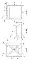
- FIGS. 7 and 8illustrate various measurements of LED chip substrate 50 .
- FIG. 7illustrates various maximum dimensions for square adjacent sides 52 and 54 .
- FIG. 8illustrates various maximum dimensions for rectangular chips where adjacent sides 52 and 54 are different, for example, where side 52 is smaller than side 54 .
- FIG. 8illustrates various dimensions of the smaller and larger sides 52 and 54 of LED chip substrate 50 thickness.
- adjacent sides 52 and 54can comprise approximately 350 ⁇ m ⁇ 470 ⁇ m and can comprise a thickness, or height, of approximately 175 ⁇ m.
- substrate thickness 50can have a height of approximately 290 ⁇ m.
- substrate thickness 50can have a height of approximately 335 ⁇ m (e.g., 0.335 mm).
- upper face 56can be a rectangle of approximately 177 ⁇ m ⁇ 297 ⁇ m in length and width. In other aspects, upper face can be a rectangle of approximately 44 ⁇ m ⁇ 164 ⁇ m in length and width.
- Such LED chips 12can have a ratio between area of upper face 56 and maximum area of adjacent sides 52 and 54 of approximately 0.4 or less. It has been found that the light extraction can be improved as the ratio of the area of upper face 56 to the maximum area of sides 52 and 54 is reduced.
- LED chips 12 selected for usehave been improved to advantageously increase light extraction efficiency.
- the ratio of LED chip size (e.g., chip length or width, previously described with respect to FIGS. 6A to 6C ) to lens 30 sizee.g., lens diameter D 1 previously described with respect to FIGS. 3A to 4
- lens 30 sizee.g., lens diameter D 1 previously described with respect to FIGS. 3A to 4
- One way to minimize such ratiois to increase lens 30 size, for example, by decreasing edge exclusion E ( FIGS. 3A, 4 ) and/or to decrease LED chip 12 size.
- LED chips 12 selected for usecan be reduced and improved with respect to other device features as described herein.
- LED chips 12can have a length and a width of approximately 0.85 mm in length or less.
- lens 30can have a lens size or diameter of approximately 2.172 mm or more (depending upon edge exclusion, E).
- the chip size to lens size (e.g., width of LED chip 12 to width or diameter of lens 30 ) ratiocan be improved to be approximately 0.4 or less.
- the chip to lens ratiocan be 0.391 or less and any sub-range including approximately 0.1 to 0.2; 0.2 to 0.3; or 0.3 to 0.4. Minimizing the ratio between chip and lens sizes can increase the light extraction efficiency.
- a ratio of width of LED chip 12 to width of submount 22can also be reduced and improved for advantageously increasing light extraction.
- the ratio between the width of LED chip 12 (e.g., maximum measurement of sides 52 and/or 54 ) to the width of submount 22can be approximately 0.35 or less. Any sub-range of ratio between approximately zero (0) and 0.35 is contemplated however, for example, 0 to 0.1; 0.1 to 0.2; 0.2 to 0.3; and greater than 0.3.
- device 10can be tuned to achieve the best possible performance relative to the device footprint. Miniaturized devices must still maintain and/or exceed brightness levels, which can be accomplished in part by reducing and improving various package dimensions and/or ratios.
Landscapes
- Led Device Packages (AREA)
Abstract
Description
Claims (44)
Priority Applications (5)
| Application Number | Priority Date | Filing Date | Title |
|---|---|---|---|
| US13/312,518US10008637B2 (en) | 2011-12-06 | 2011-12-06 | Light emitter devices and methods with reduced dimensions and improved light output |
| US13/365,682US9434219B1 (en) | 2008-01-25 | 2012-02-03 | Automated tire changer machine, systems, programs and methods |
| PCT/US2012/067326WO2013085816A1 (en) | 2011-12-06 | 2012-11-30 | Light emitter devices and methods with reduced dimensions and improved light output |
| KR1020147018718AKR20140106663A (en) | 2011-12-06 | 2012-11-30 | Light emitter devices and methods with reduced dimensions and improved light output |
| CN201280060437.3ACN103988324B (en) | 2011-12-06 | 2012-11-30 | Size reduces and light output is improved light transmitter device and method |
Applications Claiming Priority (1)
| Application Number | Priority Date | Filing Date | Title |
|---|---|---|---|
| US13/312,518US10008637B2 (en) | 2011-12-06 | 2011-12-06 | Light emitter devices and methods with reduced dimensions and improved light output |
Publications (2)
| Publication Number | Publication Date |
|---|---|
| US20130141920A1 US20130141920A1 (en) | 2013-06-06 |
| US10008637B2true US10008637B2 (en) | 2018-06-26 |
Family
ID=48523884
Family Applications (1)
| Application Number | Title | Priority Date | Filing Date |
|---|---|---|---|
| US13/312,518Active2032-10-09US10008637B2 (en) | 2008-01-25 | 2011-12-06 | Light emitter devices and methods with reduced dimensions and improved light output |
Country Status (4)
| Country | Link |
|---|---|
| US (1) | US10008637B2 (en) |
| KR (1) | KR20140106663A (en) |
| CN (1) | CN103988324B (en) |
| WO (1) | WO2013085816A1 (en) |
Cited By (3)
| Publication number | Priority date | Publication date | Assignee | Title |
|---|---|---|---|---|
| US10211380B2 (en) | 2011-07-21 | 2019-02-19 | Cree, Inc. | Light emitting devices and components having improved chemical resistance and related methods |
| US10490712B2 (en) | 2011-07-21 | 2019-11-26 | Cree, Inc. | Light emitter device packages, components, and methods for improved chemical resistance and related methods |
| US10686107B2 (en) | 2011-07-21 | 2020-06-16 | Cree, Inc. | Light emitter devices and components with improved chemical resistance and related methods |
Families Citing this family (24)
| Publication number | Priority date | Publication date | Assignee | Title |
|---|---|---|---|---|
| US10008637B2 (en) | 2011-12-06 | 2018-06-26 | Cree, Inc. | Light emitter devices and methods with reduced dimensions and improved light output |
| US9496466B2 (en) | 2011-12-06 | 2016-11-15 | Cree, Inc. | Light emitter devices and methods, utilizing light emitting diodes (LEDs), for improved light extraction |
| US9343441B2 (en) | 2012-02-13 | 2016-05-17 | Cree, Inc. | Light emitter devices having improved light output and related methods |
| US9240530B2 (en) | 2012-02-13 | 2016-01-19 | Cree, Inc. | Light emitter devices having improved chemical and physical resistance and related methods |
| JP6219586B2 (en)* | 2012-05-09 | 2017-10-25 | ローム株式会社 | Semiconductor light emitting device |
| US9234653B2 (en)* | 2013-05-13 | 2016-01-12 | Riverpoint Medical, Llc | Medical headlamp optical arrangement permitting variable beam width |
| DE102013218404A1 (en)* | 2013-09-13 | 2015-03-19 | Osram Opto Semiconductors Gmbh | Optoelectronic component and method for its production |
| KR102154061B1 (en)* | 2014-02-05 | 2020-09-09 | 엘지이노텍 주식회사 | Light emitting device package and lighting apparatus including the same |
| US10032969B2 (en) | 2014-12-26 | 2018-07-24 | Nichia Corporation | Light emitting device |
| DE102015110655A1 (en)* | 2015-07-02 | 2017-01-05 | Infineon Technologies Austria Ag | Electronic device and method of manufacturing the same |
| EP3357097B1 (en) | 2015-10-01 | 2020-12-16 | Cree, Inc. | Low optical loss flip chip solid state lighting device |
| US10062817B1 (en)* | 2017-01-10 | 2018-08-28 | Rayvio Corporation | Ultraviolet emitting device with shaped encapsulant |
| JP3219833U (en)* | 2017-08-08 | 2019-01-31 | 廈門市三安光電科技有限公司 | LED light emitting device |
| CN207818608U (en)* | 2017-11-22 | 2018-09-04 | 厦门市三安光电科技有限公司 | A kind of LED lighting device |
| US11387389B2 (en) | 2018-01-29 | 2022-07-12 | Creeled, Inc. | Reflective layers for light-emitting diodes |
| US11923481B2 (en) | 2018-01-29 | 2024-03-05 | Creeled, Inc. | Reflective layers for light-emitting diodes |
| US11031527B2 (en) | 2018-01-29 | 2021-06-08 | Creeled, Inc. | Reflective layers for light-emitting diodes |
| US10879441B2 (en) | 2018-12-17 | 2020-12-29 | Cree, Inc. | Interconnects for light emitting diode chips |
| US10985294B2 (en) | 2019-03-19 | 2021-04-20 | Creeled, Inc. | Contact structures for light emitting diode chips |
| JP1655194S (en)* | 2019-06-04 | 2020-03-16 | ||
| JP1655195S (en)* | 2019-06-04 | 2020-03-16 | ||
| US11094848B2 (en) | 2019-08-16 | 2021-08-17 | Creeled, Inc. | Light-emitting diode chip structures |
| USD996378S1 (en)* | 2022-03-09 | 2023-08-22 | Creeled, Inc. | Light-emitting diode package |
| US12355013B2 (en) | 2022-04-21 | 2025-07-08 | Creeled, Inc. | Emission height arrangements in light-emitting diode packages and related devices and methods |
Citations (189)
| Publication number | Priority date | Publication date | Assignee | Title |
|---|---|---|---|---|
| US3288728A (en) | 1966-02-18 | 1966-11-29 | Union Carbide Corp | Para-xylylene copolymers |
| US3609475A (en) | 1970-05-04 | 1971-09-28 | Hewlett Packard Co | Light-emitting diode package with dual-colored plastic encapsulation |
| US3875456A (en) | 1972-04-04 | 1975-04-01 | Hitachi Ltd | Multi-color semiconductor lamp |
| JPS5867077A (en) | 1981-10-19 | 1983-04-21 | Toshiba Corp | Manufacture of lead frame for semiconductor device |
| USH445H (en) | 1985-11-29 | 1988-03-01 | American Telephone and Telegraph Company, AT&T Technologies, Incorporated | Method of forming light emitting device with direct contact lens |
| US4918497A (en) | 1988-12-14 | 1990-04-17 | Cree Research, Inc. | Blue light emitting diode formed in silicon carbide |
| US4946547A (en) | 1989-10-13 | 1990-08-07 | Cree Research, Inc. | Method of preparing silicon carbide surfaces for crystal growth |
| US4966862A (en) | 1989-08-28 | 1990-10-30 | Cree Research, Inc. | Method of production of light emitting diodes |
| US5027168A (en) | 1988-12-14 | 1991-06-25 | Cree Research, Inc. | Blue light emitting diode formed in silicon carbide |
| US5200022A (en) | 1990-10-03 | 1993-04-06 | Cree Research, Inc. | Method of improving mechanically prepared substrate surfaces of alpha silicon carbide for deposition of beta silicon carbide thereon and resulting product |
| US5210051A (en) | 1990-03-27 | 1993-05-11 | Cree Research, Inc. | High efficiency light emitting diodes from bipolar gallium nitride |
| US5338944A (en) | 1993-09-22 | 1994-08-16 | Cree Research, Inc. | Blue light-emitting diode with degenerate junction structure |
| US5359345A (en) | 1992-08-05 | 1994-10-25 | Cree Research, Inc. | Shuttered and cycled light emitting diode display and method of producing the same |
| USRE34861E (en) | 1987-10-26 | 1995-02-14 | North Carolina State University | Sublimation of silicon carbide to produce large, device quality single crystals of silicon carbide |
| US5393993A (en) | 1993-12-13 | 1995-02-28 | Cree Research, Inc. | Buffer structure between silicon carbide and gallium nitride and resulting semiconductor devices |
| US5416342A (en) | 1993-06-23 | 1995-05-16 | Cree Research, Inc. | Blue light-emitting diode with high external quantum efficiency |
| US5523589A (en) | 1994-09-20 | 1996-06-04 | Cree Research, Inc. | Vertical geometry light emitting diode with group III nitride active layer and extended lifetime |
| US5604135A (en) | 1994-08-12 | 1997-02-18 | Cree Research, Inc. | Method of forming green light emitting diode in silicon carbide |
| US5631190A (en) | 1994-10-07 | 1997-05-20 | Cree Research, Inc. | Method for producing high efficiency light-emitting diodes and resulting diode structures |
| US5739554A (en) | 1995-05-08 | 1998-04-14 | Cree Research, Inc. | Double heterojunction light emitting diode with gallium nitride active layer |
| US5959316A (en) | 1998-09-01 | 1999-09-28 | Hewlett-Packard Company | Multiple encapsulation of phosphor-LED devices |
| US6121637A (en)* | 1997-10-03 | 2000-09-19 | Rohm Co., Ltd. | Semiconductor light emitting device with increased luminous power |
| US6187606B1 (en) | 1997-10-07 | 2001-02-13 | Cree, Inc. | Group III nitride photonic devices on silicon carbide substrates with conductive buffer interlayer structure |
| US6252254B1 (en) | 1998-02-06 | 2001-06-26 | General Electric Company | Light emitting device with phosphor composition |
| JP2001291406A (en) | 2000-04-07 | 2001-10-19 | Yamada Shomei Kk | Lighting |
| US20020004577A1 (en) | 1996-07-10 | 2002-01-10 | International Business Machines Corporation | Siloxane and siloxane derivatives as encapsulants for organic light emitting devices |
| US6350041B1 (en) | 1999-12-03 | 2002-02-26 | Cree Lighting Company | High output radial dispersing lamp using a solid state light source |
| US20030067761A1 (en)* | 2001-10-09 | 2003-04-10 | Citizen Electronics Co., Ltd. | Edge light for a lighting panel |
| US6576930B2 (en) | 1996-06-26 | 2003-06-10 | Osram Opto Semiconductors Gmbh | Light-radiating semiconductor component with a luminescence conversion element |
| US6600175B1 (en) | 1996-03-26 | 2003-07-29 | Advanced Technology Materials, Inc. | Solid state white light emitter and display using same |
| JP2003243704A (en) | 2002-02-07 | 2003-08-29 | Lumileds Lighting Us Llc | Light emitting semiconductor device and method |
| US6717353B1 (en) | 2002-10-14 | 2004-04-06 | Lumileds Lighting U.S., Llc | Phosphor converted light emitting device |
| US20040079957A1 (en) | 2002-09-04 | 2004-04-29 | Andrews Peter Scott | Power surface mount light emitting die package |
| WO2004077580A2 (en) | 2003-02-26 | 2004-09-10 | Cree, Inc. | White light source using emitting diode and phosphor and method of fabrication |
| US6791119B2 (en) | 2001-02-01 | 2004-09-14 | Cree, Inc. | Light emitting diodes including modifications for light extraction |
| US20040252501A1 (en) | 2002-04-24 | 2004-12-16 | Hideo Moriyama | Light source coupler, illuminant device, patterned conductor, and method for manufacturing light source coupler |
| US20050007783A1 (en)* | 2003-07-09 | 2005-01-13 | Masato Ono | Light emitting device, method of manufacturing the same and lighting equipment |
| US6853010B2 (en) | 2002-09-19 | 2005-02-08 | Cree, Inc. | Phosphor-coated light emitting diodes including tapered sidewalls, and fabrication methods therefor |
| US6860621B2 (en) | 2000-07-10 | 2005-03-01 | Osram Opto Semiconductors Gmbh | LED module and methods for producing and using the module |
| US20050045898A1 (en) | 2003-09-03 | 2005-03-03 | Charles Leu | Light-emitting diode and backlight system using the same |
| EP1536487A1 (en) | 2002-05-28 | 2005-06-01 | Matsushita Electric Works, Ltd. | Light emitting element, light emitting device and surface emission illuminating device using it |
| US20050159581A1 (en) | 2003-10-22 | 2005-07-21 | Dirk Vanderzande | Method of preparing derivatives of polyarylene vinylene and method of preparing an electronic device including same |
| US6936857B2 (en) | 2003-02-18 | 2005-08-30 | Gelcore, Llc | White light LED device |
| JP2005244226A (en) | 2004-02-23 | 2005-09-08 | Lumileds Lighting Us Llc | Wavelength conversion type semiconductor light emitting device |
| US20050194609A1 (en) | 2000-07-31 | 2005-09-08 | Kabushiki Kaisha Toshiba | Semiconductor light emitting device and method for manufacturing same |
| US20050224830A1 (en) | 2004-04-09 | 2005-10-13 | Blonder Greg E | Illumination devices comprising white light emitting diodes and diode arrays and method and apparatus for making them |
| US6958497B2 (en) | 2001-05-30 | 2005-10-25 | Cree, Inc. | Group III nitride based light emitting diode structures with a quantum well and superlattice, group III nitride based quantum well structures and group III nitride based superlattice structures |
| JP2006054209A (en) | 2003-09-30 | 2006-02-23 | Toyoda Gosei Co Ltd | Light emitting device |
| US7005679B2 (en) | 2003-05-01 | 2006-02-28 | Cree, Inc. | Multiple component solid state white light |
| US7026661B2 (en) | 2001-06-11 | 2006-04-11 | Citizen Electronics Co., Ltd. | Light emitting device and manufacturing method thereof |
| US20060091788A1 (en) | 2004-10-29 | 2006-05-04 | Ledengin, Inc. | Light emitting device with a thermal insulating and refractive index matching material |
| US20060091415A1 (en) | 2004-10-29 | 2006-05-04 | Ledengin, Inc. (Cayman) | LED package with structure and materials for high heat dissipation |
| US20060105484A1 (en) | 2004-11-15 | 2006-05-18 | Grigoriy Basin | Molded lens over LED die |
| US20060113906A1 (en) | 2004-11-29 | 2006-06-01 | Satoru Ogawa | Light emitting device and method for manufacturing thereof |
| US20060124953A1 (en) | 2004-12-14 | 2006-06-15 | Negley Gerald H | Semiconductor light emitting device mounting substrates and packages including cavities and cover plates, and methods of packaging same |
| US20060138621A1 (en) | 2002-09-30 | 2006-06-29 | Osram Opto Semiconductors Gmbh | Optoelectronic component and a module based thereon |
| US20060145172A1 (en) | 2004-12-30 | 2006-07-06 | Jung-Chieh Su | Light emitting diode with a quasi-omnidirectional reflector |
| US20060163589A1 (en) | 2005-01-21 | 2006-07-27 | Zhaoyang Fan | Heterogeneous integrated high voltage DC/AC light emitter |
| US7087936B2 (en) | 2003-04-30 | 2006-08-08 | Cree, Inc. | Methods of forming light-emitting devices having an antireflective layer that has a graded index of refraction |
| US20060181866A1 (en) | 2005-02-16 | 2006-08-17 | Samsung Electronics Co., Ltd. | Multi-chip light emitting diode unit, and backlight unit and liquid crystal display device employing the same |
| US7095056B2 (en) | 2003-12-10 | 2006-08-22 | Sensor Electronic Technology, Inc. | White light emitting device and method |
| US20060186418A1 (en) | 2004-05-18 | 2006-08-24 | Edmond John A | External extraction light emitting diode based upon crystallographic faceted surfaces |
| JP2006245443A (en) | 2005-03-07 | 2006-09-14 | Citizen Electronics Co Ltd | Light emitting device and lighting device |
| US20060221272A1 (en) | 2005-04-04 | 2006-10-05 | Negley Gerald H | Light emitting diode backlighting systems and methods that use more colors than display picture elements |
| US20060226759A1 (en) | 2005-03-06 | 2006-10-12 | Sharp Kabushiki Kaisha | Light emitting device and fabricating method thereof |
| US20070012940A1 (en) | 2005-07-14 | 2007-01-18 | Samsung Electro-Mechanics Co., Ltd. | Wavelength-convertible light emitting diode package |
| US7183577B2 (en) | 1999-09-27 | 2007-02-27 | Philips Lumileds Lighting Company, Llc | Thin film phosphor-converted light emitting diode device |
| KR100705552B1 (en) | 2006-06-30 | 2007-04-09 | 서울반도체 주식회사 | Light emitting diode |
| US20070090383A1 (en) | 2000-12-28 | 2007-04-26 | Toyoda Gosei Co., Ltd. | Light emitting device |
| US7213940B1 (en) | 2005-12-21 | 2007-05-08 | Led Lighting Fixtures, Inc. | Lighting device and lighting method |
| US20070139923A1 (en) | 2005-12-21 | 2007-06-21 | Led Lighting Fixtures, Inc. | Lighting device |
| US20070158668A1 (en) | 2005-08-25 | 2007-07-12 | Cree, Inc. | Close loop electrophoretic deposition of semiconductor devices |
| US7246930B2 (en) | 2003-09-17 | 2007-07-24 | Stanley Electric Co., Ltd. | Light source and vehicle lamp |
| US20070170447A1 (en) | 2006-01-20 | 2007-07-26 | Led Lighting Fixtures, Inc. | Shifting spectral content in solid state light emitters by spatially separating lumiphor films |
| KR20070084959A (en) | 2006-02-22 | 2007-08-27 | 삼성전기주식회사 | LED Package |
| US20070223219A1 (en) | 2005-01-10 | 2007-09-27 | Cree, Inc. | Multi-chip light emitting device lamps for providing high-cri warm white light and light fixtures including the same |
| CN101047220A (en) | 2006-03-29 | 2007-10-03 | 丰田合成株式会社 | Light emitting device |
| US20070228387A1 (en) | 2006-04-04 | 2007-10-04 | Gerald Negley | Uniform emission LED package |
| KR20070100124A (en) | 2006-04-05 | 2007-10-10 | 샤프 가부시키가이샤 | Semiconductor light emitting device |
| US20070253209A1 (en) | 2006-04-27 | 2007-11-01 | Cree, Inc. | Submounts for semiconductor light emitting device packages and semiconductor light emitting device packages including the same |
| US20070268694A1 (en) | 2006-04-18 | 2007-11-22 | Lamina Ceramics, Inc. | Optical devices for controlled color mixing |
| US7304326B2 (en) | 2004-02-06 | 2007-12-04 | Toyoda Gosei Co., Ltd. | Light emitting device and sealing material |
| US20080012036A1 (en) | 2006-07-13 | 2008-01-17 | Loh Ban P | Leadframe-based packages for solid state light emitting devices and methods of forming leadframe-based packages for solid state light emitting devices |
| US7344902B2 (en) | 2004-11-15 | 2008-03-18 | Philips Lumileds Lighting Company, Llc | Overmolded lens over LED die |
| US20080081065A1 (en) | 2002-03-22 | 2008-04-03 | Govermment of the United States of America, represente by the Secretary, Department of Health | Materials and methods for inhibiting wip1 |
| US20080080165A1 (en) | 2006-10-02 | 2008-04-03 | Samsung Electro-Mechanics Co. Ltd. | Surface light source device using light emitting diodes |
| TW200821371A (en) | 2006-08-22 | 2008-05-16 | Mitsubishi Chem Corp | Semiconductor device member, liquid for forming semiconductor device member, method for manufacturing semiconductor device member, and liquid for forming semiconductor device member using the method, phosphor composition, semiconductor light emitting |
| US20080121921A1 (en) | 2006-07-13 | 2008-05-29 | Cree, Inc. | Leadframe-based packages for solid state light emitting devices and methods of forming leadframe-based packages for solid state light emitting devices |
| US20080173884A1 (en) | 2007-01-22 | 2008-07-24 | Cree, Inc. | Wafer level phosphor coating method and devices fabricated utilizing method |
| US20080179617A1 (en) | 2007-01-18 | 2008-07-31 | Citizen Electronics Co., Ltd. | Semiconductor light-emitting device |
| US20080179611A1 (en)* | 2007-01-22 | 2008-07-31 | Cree, Inc. | Wafer level phosphor coating method and devices fabricated utilizing method |
| US20080198112A1 (en) | 2007-02-15 | 2008-08-21 | Cree, Inc. | Partially filterless liquid crystal display devices and methods of operating the same |
| CN101276870A (en) | 2007-03-27 | 2008-10-01 | 株式会社东芝 | Semiconductor light emitting device and manufacturing method thereof |
| US20080239724A1 (en) | 2004-03-24 | 2008-10-02 | Toshiba Lighting & Technology Corporation | Illuminating Device |
| US20080258130A1 (en) | 2007-04-23 | 2008-10-23 | Bergmann Michael J | Beveled LED Chip with Transparent Substrate |
| US7456499B2 (en) | 2004-06-04 | 2008-11-25 | Cree, Inc. | Power light emitting die package with reflecting lens and the method of making the same |
| US20080303052A1 (en) | 2004-09-10 | 2008-12-11 | Seoul Semiconductor Co., Ltd. | Light emitting diode package having multiple molding resins |
| US20080308825A1 (en) | 2007-06-14 | 2008-12-18 | Cree, Inc. | Encapsulant with scatterer to tailor spatial emission pattern and color uniformity in light emitting diodes |
| US7476909B2 (en)* | 2004-12-20 | 2009-01-13 | Sumitomo Electric Industries, Ltd. | Light emitting device |
| TW200903859A (en) | 2007-03-12 | 2009-01-16 | Nichia Corp | High power light emitting device and package for using the same |
| US20090039375A1 (en) | 2007-08-07 | 2009-02-12 | Cree, Inc. | Semiconductor light emitting devices with separated wavelength conversion materials and methods of forming the same |
| US20090050924A1 (en) | 2007-06-11 | 2009-02-26 | Cree, Inc. | Droop-free high output light emitting devices and methods of fabricating and operating same |
| US20090050907A1 (en) | 2005-01-10 | 2009-02-26 | Cree, Inc. | Solid state lighting component |
| US20090050908A1 (en) | 2005-01-10 | 2009-02-26 | Cree, Inc. | Solid state lighting component |
| US20090065792A1 (en) | 2007-09-07 | 2009-03-12 | 3M Innovative Properties Company | Method of making an led device having a dome lens |
| US20090080185A1 (en)* | 2007-09-25 | 2009-03-26 | Cree, Inc. | LED multi-chip lighting units and related methods |
| US20090108281A1 (en) | 2007-10-31 | 2009-04-30 | Cree, Inc. | Light emitting diode package and method for fabricating same |
| US7534635B1 (en) | 2008-03-24 | 2009-05-19 | General Electric Company | Getter precursors for hermetically sealed packaging |
| US20090179213A1 (en) | 2008-01-15 | 2009-07-16 | Cree, Inc. | Phosphor coating systems and methods for light emitting structures and packaged light emitting diodes including phosphor coating |
| US7564180B2 (en) | 2005-01-10 | 2009-07-21 | Cree, Inc. | Light emission device and method utilizing multiple emitters and multiple phosphors |
| US20090184616A1 (en) | 2007-10-10 | 2009-07-23 | Cree Led Lighting Solutions, Inc. | Lighting device and method of making |
| JP2009170825A (en) | 2008-01-19 | 2009-07-30 | Nichia Corp | Light emitting device and manufacturing method thereof |
| US20090194782A1 (en) | 2008-02-06 | 2009-08-06 | Sharp Kabushiki Kaisha | Semiconductor light emitting device |
| US20090212316A1 (en)* | 2005-08-30 | 2009-08-27 | Osram Opto Semiconductors Gmbh | Surface-mounted optoelectronic semiconductor component and method for the production thereof |
| WO2009107052A1 (en) | 2008-02-27 | 2009-09-03 | Koninklijke Philips Electronics N.V. | Illumination device with led and one or more transmissive windows |
| US20090231833A1 (en)* | 2005-02-18 | 2009-09-17 | Tomohide Miki | Light emitting device provided with lens for controlling light distribution characteristic |
| US20090236621A1 (en) | 2008-03-19 | 2009-09-24 | Cree, Inc. | Low index spacer layer in LED devices |
| JP2009224536A (en) | 2008-03-17 | 2009-10-01 | Citizen Holdings Co Ltd | Led device and method of manufacturing the same |
| US7598669B2 (en) | 2002-03-29 | 2009-10-06 | Samsung Mobile Display Co., Ltd. | Light-emitting diode, its manufacturing method, and display device using the same |
| US20090250714A1 (en) | 2008-04-03 | 2009-10-08 | Samsung Electro-Mechanics Co., Ltd. | White light emitting diode and lighting apparatus using the same |
| US20090283779A1 (en) | 2007-06-14 | 2009-11-19 | Cree, Inc. | Light source with near field mixing |
| US20090295265A1 (en) | 2004-12-24 | 2009-12-03 | Kyocera Corporation | Light Emitting Device and Illumination Apparatus |
| US20090315057A1 (en)* | 2008-06-24 | 2009-12-24 | Sharp Kabushiki Kaisha | Light-emitting apparatus, surface light source, and method for manufacturing package for light-emitting apparatus |
| US7638811B2 (en) | 2007-03-13 | 2009-12-29 | Cree, Inc. | Graded dielectric layer |
| JP2010007013A (en) | 2008-06-30 | 2010-01-14 | Jsr Corp | Coating material for metal surface, light emitter, and method for protecting metal surface |
| US20100025709A1 (en) | 2008-07-29 | 2010-02-04 | Toyoda Gosei Co., Ltd. | Light emitting device |
| US20100025699A1 (en) | 2008-07-30 | 2010-02-04 | Lustrous International Technology Ltd. | Light emitting diode chip package |
| JP2010092956A (en) | 2008-10-06 | 2010-04-22 | Mitsubishi Electric Corp | Led light source and luminary using it |
| US20100103660A1 (en) | 2008-10-24 | 2010-04-29 | Cree Led Lighting Solutions, Inc. | Array layout for color mixing |
| US20100102344A1 (en) | 2007-03-01 | 2010-04-29 | Yoshinori Ueji | Led device and illuminating apparatus |
| US7709853B2 (en) | 2007-02-12 | 2010-05-04 | Cree, Inc. | Packaged semiconductor light emitting devices having multiple optical elements |
| JP2010103404A (en) | 2008-10-27 | 2010-05-06 | Sanyo Electric Co Ltd | Lighting device |
| US20100133556A1 (en) | 2009-06-18 | 2010-06-03 | Bridgelux, Inc. | Led array package covered with a highly thermal conductive plate |
| US20100155763A1 (en) | 2008-01-15 | 2010-06-24 | Cree, Inc. | Systems and methods for application of optical materials to optical elements |
| KR20100079970A (en) | 2008-12-31 | 2010-07-08 | 서울반도체 주식회사 | Light source package |
| KR20100086955A (en) | 2009-01-23 | 2010-08-02 | 신에쓰 가가꾸 고교 가부시끼가이샤 | Primer composition and optical semiconductor device using the same |
| US20100203657A1 (en) | 2009-02-09 | 2010-08-12 | Samsung Electronics Co., Ltd. | Method of fabricating light emitting device |
| US20100200874A1 (en) | 2007-09-03 | 2010-08-12 | National Institute For Materials Science | Phosphor, method for producing the same and light-emitting device using the same |
| US20100208487A1 (en) | 2009-02-13 | 2010-08-19 | PerkinElmer LED Solutions, Inc. | Led illumination device |
| CN101814571A (en) | 2009-02-24 | 2010-08-25 | 信越化学工业株式会社 | Optical semiconductor device encapsulated with silicone resin |
| US20100226130A1 (en) | 2009-03-04 | 2010-09-09 | Unilumin Group Co., Ltd. | Led light module for street lamp and method of manufacturing same |
| JP2010206015A (en) | 2009-03-04 | 2010-09-16 | Toyoda Gosei Co Ltd | Method of manufacturing light emitting device |
| US20100237375A1 (en) | 2007-12-07 | 2010-09-23 | Panasonic Electric Works Co., Ltd. | Light Emitting Device |
| WO2010113852A1 (en) | 2009-03-31 | 2010-10-07 | 東芝ライテック株式会社 | Light-emitting device and illumination device |
| US20100252851A1 (en)* | 2007-10-31 | 2010-10-07 | Cree, Inc. | Led package with increased feature sizes |
| US20100258830A1 (en) | 2007-11-19 | 2010-10-14 | Yoshiyuki Ide | Semiconductor light-emitting device and manufacturing method of the same |
| US7825575B2 (en) | 2005-09-13 | 2010-11-02 | Sumita Optical Glass, Inc. | Solid-state element device and light-emitting apparatus using same |
| US20100283381A1 (en) | 2005-09-06 | 2010-11-11 | Sharp Kabushiki Kaisha | Phosphor and light emitting device |
| US20100289395A1 (en)* | 2009-05-13 | 2010-11-18 | Light Prescriptions Innovators, Llc | Dimmable led lamp |
| US7842526B2 (en) | 2004-09-09 | 2010-11-30 | Toyoda Gosei Co., Ltd. | Light emitting device and method of producing same |
| US20110001148A1 (en) | 2009-07-06 | 2011-01-06 | Zhuo Sun | Thin flat solid state light source module |
| US7868343B2 (en) | 2004-04-06 | 2011-01-11 | Cree, Inc. | Light-emitting devices having multiple encapsulation layers with at least one of the encapsulation layers including nanoparticles and methods of forming the same |
| US20110031513A1 (en) | 2009-08-04 | 2011-02-10 | Advanced Optoelectronic Technology, Inc. | Waterproof smd led module and method of manufacturing the same |
| US20110046319A1 (en) | 2009-08-21 | 2011-02-24 | Shin-Etsu Chemical Co., Ltd. | Organopolysilmethylene and a cured product thereof |
| US20110108875A1 (en) | 2008-06-25 | 2011-05-12 | Sharp Kabushiki Kaisha | Light-emitting device and method for producing same |
| US7952115B2 (en) | 2006-05-31 | 2011-05-31 | Cree, Inc. | Packaged light emitting devices including multiple index lenses and methods of fabricating the same |
| JP2011127011A (en) | 2009-12-18 | 2011-06-30 | Sekisui Chem Co Ltd | Sealant for optical semiconductor device and optical semiconductor device produced by using the same |
| JP2011134508A (en) | 2009-12-22 | 2011-07-07 | Panasonic Electric Works Co Ltd | Lighting fixture |
| CN201918428U (en) | 2010-12-28 | 2011-08-03 | 广州市鸿利光电股份有限公司 | Vulcanization-preventive surface-mounted LED |
| CN102150480A (en) | 2008-08-18 | 2011-08-10 | 赛姆布兰特环球有限公司 | Halocarbon polymer coating |
| CN102163680A (en) | 2010-02-19 | 2011-08-24 | 旭硝子株式会社 | Substrate for mounting light-emitting element and light-emitting device |
| US8011818B2 (en) | 2006-11-13 | 2011-09-06 | Cree, Inc. | Lighting device including plural optical structures having at least two different refraction indices, and lighting methods |
| WO2011109097A1 (en) | 2010-03-03 | 2011-09-09 | Cree, Inc. | Enhanced color rendering index emitter through phosphor separation |
| EP2365549A1 (en) | 2010-03-12 | 2011-09-14 | Asahi Glass Company, Limited | Light-emitting device |
| US20110220929A1 (en) | 2010-03-09 | 2011-09-15 | Cree, Inc. | Warm white leds having high color rendering index values and related luminophoric mediums |
| US20110220920A1 (en) | 2010-03-09 | 2011-09-15 | Brian Thomas Collins | Methods of forming warm white light emitting devices having high color rendering index values and related light emitting devices |
| US20110242806A1 (en) | 2010-03-31 | 2011-10-06 | Renaissance Lighting, Inc. | Solid state lighting with selective matching of index of refraction |
| US20110241049A1 (en) | 2010-04-02 | 2011-10-06 | Asahi Glass Company, Limited | Substrate for mounting light-emitting element and light-emitting device employing the substrate |
| CN102214776A (en) | 2010-04-09 | 2011-10-12 | 亿广科技(上海)有限公司 | Light emitting diode package, lighting device and light emitting diode package substrate |
| US20110248289A1 (en) | 2010-04-09 | 2011-10-13 | Everlight Electronics Co., Ltd. | Light emitting diode package, lighting device and light emitting diode package substrate |
| US8052307B2 (en) | 2009-11-19 | 2011-11-08 | Lg Innotek Co., Ltd. | Lens and light emitting apparatus having the same |
| US20110272721A1 (en)* | 2010-05-07 | 2011-11-10 | Philips Lumileds Lighting Company, Llc | Led package with a rounded square lens |
| US20110278618A1 (en) | 2010-05-14 | 2011-11-17 | Asahi Glass Company, Limited | Substrate for mounting light-emitting element and light-emitting device |
| US20110284897A1 (en) | 2010-05-18 | 2011-11-24 | Stanley Electric Co., Ltd. | Semiconductor light emitting device |
| US20120126257A1 (en) | 2010-11-22 | 2012-05-24 | Jesse Colin Reiherzer | Light emitting devices and methods |
| US20120161621A1 (en) | 2010-12-28 | 2012-06-28 | Nichia Corporation | Light emitting device |
| US20120193660A1 (en) | 2011-01-31 | 2012-08-02 | Cree, Inc. | Horizontal light emitting diodes including phosphor particles |
| US20120193649A1 (en) | 2011-01-31 | 2012-08-02 | Matthew Donofrio | Light emitting diode (led) arrays including direct die attach and related assemblies |
| US20130020590A1 (en) | 2011-07-21 | 2013-01-24 | Shaow Lin | Light emitting devices and components having excellent chemical resistance and related methods |
| WO2013013154A2 (en) | 2011-07-21 | 2013-01-24 | Cree, Inc. | Light emitter device packages, components, and methods for improved chemical resistance and related methods |
| WO2013082445A1 (en) | 2011-12-01 | 2013-06-06 | Cree, Inc. | Light emitter devices and components with improved chemical resistance and related methods |
| US20130141905A1 (en) | 2011-12-06 | 2013-06-06 | Cree, Inc. | Light emitter devices and methods for improved light extraction |
| WO2013085816A1 (en) | 2011-12-06 | 2013-06-13 | Cree, Inc. | Light emitter devices and methods with reduced dimensions and improved light output |
| US20130161650A1 (en) | 2009-10-02 | 2013-06-27 | Taiwan Semiconductor Manufacturing Co., Ltd. | Device with self aligned stressor and method of making same |
| US20130168719A1 (en) | 2010-03-02 | 2013-07-04 | Micron Technology, Inc. | Method for forming a light conversion material |
| US20130207130A1 (en) | 2012-02-13 | 2013-08-15 | Jesse Colin Reiherzer | Light emitter devices having improved light output and related methods |
| US20130207142A1 (en) | 2012-02-13 | 2013-08-15 | Jesse Colin Reiherzer | Light emitter devices having improved chemical and physical resistance and related methods |
| US20130208442A1 (en) | 2012-02-13 | 2013-08-15 | Cree, Inc. | Lighting device including multiple wavelength conversion material layers |
| US20130207141A1 (en) | 2012-02-13 | 2013-08-15 | Cree, Inc. | Lighting device including multiple encapsulant material layers |
- 2011
- 2011-12-06USUS13/312,518patent/US10008637B2/enactiveActive
- 2012
- 2012-11-30CNCN201280060437.3Apatent/CN103988324B/enactiveActive
- 2012-11-30KRKR1020147018718Apatent/KR20140106663A/ennot_activeCeased
- 2012-11-30WOPCT/US2012/067326patent/WO2013085816A1/enactiveApplication Filing
Patent Citations (234)
| Publication number | Priority date | Publication date | Assignee | Title |
|---|---|---|---|---|
| US3288728A (en) | 1966-02-18 | 1966-11-29 | Union Carbide Corp | Para-xylylene copolymers |
| US3609475A (en) | 1970-05-04 | 1971-09-28 | Hewlett Packard Co | Light-emitting diode package with dual-colored plastic encapsulation |
| US3875456A (en) | 1972-04-04 | 1975-04-01 | Hitachi Ltd | Multi-color semiconductor lamp |
| JPS5867077A (en) | 1981-10-19 | 1983-04-21 | Toshiba Corp | Manufacture of lead frame for semiconductor device |
| USH445H (en) | 1985-11-29 | 1988-03-01 | American Telephone and Telegraph Company, AT&T Technologies, Incorporated | Method of forming light emitting device with direct contact lens |
| USRE34861E (en) | 1987-10-26 | 1995-02-14 | North Carolina State University | Sublimation of silicon carbide to produce large, device quality single crystals of silicon carbide |
| US5027168A (en) | 1988-12-14 | 1991-06-25 | Cree Research, Inc. | Blue light emitting diode formed in silicon carbide |
| US4918497A (en) | 1988-12-14 | 1990-04-17 | Cree Research, Inc. | Blue light emitting diode formed in silicon carbide |
| US4966862A (en) | 1989-08-28 | 1990-10-30 | Cree Research, Inc. | Method of production of light emitting diodes |
| US4946547A (en) | 1989-10-13 | 1990-08-07 | Cree Research, Inc. | Method of preparing silicon carbide surfaces for crystal growth |
| US5210051A (en) | 1990-03-27 | 1993-05-11 | Cree Research, Inc. | High efficiency light emitting diodes from bipolar gallium nitride |
| US5200022A (en) | 1990-10-03 | 1993-04-06 | Cree Research, Inc. | Method of improving mechanically prepared substrate surfaces of alpha silicon carbide for deposition of beta silicon carbide thereon and resulting product |
| US5359345A (en) | 1992-08-05 | 1994-10-25 | Cree Research, Inc. | Shuttered and cycled light emitting diode display and method of producing the same |
| US5416342A (en) | 1993-06-23 | 1995-05-16 | Cree Research, Inc. | Blue light-emitting diode with high external quantum efficiency |
| US5338944A (en) | 1993-09-22 | 1994-08-16 | Cree Research, Inc. | Blue light-emitting diode with degenerate junction structure |
| US5393993A (en) | 1993-12-13 | 1995-02-28 | Cree Research, Inc. | Buffer structure between silicon carbide and gallium nitride and resulting semiconductor devices |
| US5604135A (en) | 1994-08-12 | 1997-02-18 | Cree Research, Inc. | Method of forming green light emitting diode in silicon carbide |
| US5523589A (en) | 1994-09-20 | 1996-06-04 | Cree Research, Inc. | Vertical geometry light emitting diode with group III nitride active layer and extended lifetime |
| US5912477A (en) | 1994-10-07 | 1999-06-15 | Cree Research, Inc. | High efficiency light emitting diodes |
| US5631190A (en) | 1994-10-07 | 1997-05-20 | Cree Research, Inc. | Method for producing high efficiency light-emitting diodes and resulting diode structures |
| US6120600A (en) | 1995-05-08 | 2000-09-19 | Cree, Inc. | Double heterojunction light emitting diode with gallium nitride active layer |
| US5739554A (en) | 1995-05-08 | 1998-04-14 | Cree Research, Inc. | Double heterojunction light emitting diode with gallium nitride active layer |
| US6600175B1 (en) | 1996-03-26 | 2003-07-29 | Advanced Technology Materials, Inc. | Solid state white light emitter and display using same |
| US6576930B2 (en) | 1996-06-26 | 2003-06-10 | Osram Opto Semiconductors Gmbh | Light-radiating semiconductor component with a luminescence conversion element |
| US20020004577A1 (en) | 1996-07-10 | 2002-01-10 | International Business Machines Corporation | Siloxane and siloxane derivatives as encapsulants for organic light emitting devices |
| US6121637A (en)* | 1997-10-03 | 2000-09-19 | Rohm Co., Ltd. | Semiconductor light emitting device with increased luminous power |
| US6187606B1 (en) | 1997-10-07 | 2001-02-13 | Cree, Inc. | Group III nitride photonic devices on silicon carbide substrates with conductive buffer interlayer structure |
| US6201262B1 (en) | 1997-10-07 | 2001-03-13 | Cree, Inc. | Group III nitride photonic devices on silicon carbide substrates with conductive buffer interlay structure |
| US6252254B1 (en) | 1998-02-06 | 2001-06-26 | General Electric Company | Light emitting device with phosphor composition |
| US5959316A (en) | 1998-09-01 | 1999-09-28 | Hewlett-Packard Company | Multiple encapsulation of phosphor-LED devices |
| US7183577B2 (en) | 1999-09-27 | 2007-02-27 | Philips Lumileds Lighting Company, Llc | Thin film phosphor-converted light emitting diode device |
| US6350041B1 (en) | 1999-12-03 | 2002-02-26 | Cree Lighting Company | High output radial dispersing lamp using a solid state light source |
| JP2001291406A (en) | 2000-04-07 | 2001-10-19 | Yamada Shomei Kk | Lighting |
| US6860621B2 (en) | 2000-07-10 | 2005-03-01 | Osram Opto Semiconductors Gmbh | LED module and methods for producing and using the module |
| US20050194609A1 (en) | 2000-07-31 | 2005-09-08 | Kabushiki Kaisha Toshiba | Semiconductor light emitting device and method for manufacturing same |
| US20070090383A1 (en) | 2000-12-28 | 2007-04-26 | Toyoda Gosei Co., Ltd. | Light emitting device |
| US6791119B2 (en) | 2001-02-01 | 2004-09-14 | Cree, Inc. | Light emitting diodes including modifications for light extraction |
| US6958497B2 (en) | 2001-05-30 | 2005-10-25 | Cree, Inc. | Group III nitride based light emitting diode structures with a quantum well and superlattice, group III nitride based quantum well structures and group III nitride based superlattice structures |
| US7026661B2 (en) | 2001-06-11 | 2006-04-11 | Citizen Electronics Co., Ltd. | Light emitting device and manufacturing method thereof |
| US20030067761A1 (en)* | 2001-10-09 | 2003-04-10 | Citizen Electronics Co., Ltd. | Edge light for a lighting panel |
| JP2003243704A (en) | 2002-02-07 | 2003-08-29 | Lumileds Lighting Us Llc | Light emitting semiconductor device and method |
| US20080081065A1 (en) | 2002-03-22 | 2008-04-03 | Govermment of the United States of America, represente by the Secretary, Department of Health | Materials and methods for inhibiting wip1 |
| US7598669B2 (en) | 2002-03-29 | 2009-10-06 | Samsung Mobile Display Co., Ltd. | Light-emitting diode, its manufacturing method, and display device using the same |
| US20040252501A1 (en) | 2002-04-24 | 2004-12-16 | Hideo Moriyama | Light source coupler, illuminant device, patterned conductor, and method for manufacturing light source coupler |
| EP1536487A1 (en) | 2002-05-28 | 2005-06-01 | Matsushita Electric Works, Ltd. | Light emitting element, light emitting device and surface emission illuminating device using it |
| US20040079957A1 (en) | 2002-09-04 | 2004-04-29 | Andrews Peter Scott | Power surface mount light emitting die package |
| US7244965B2 (en)* | 2002-09-04 | 2007-07-17 | Cree Inc, | Power surface mount light emitting die package |
| US6853010B2 (en) | 2002-09-19 | 2005-02-08 | Cree, Inc. | Phosphor-coated light emitting diodes including tapered sidewalls, and fabrication methods therefor |
| US20060138621A1 (en) | 2002-09-30 | 2006-06-29 | Osram Opto Semiconductors Gmbh | Optoelectronic component and a module based thereon |
| US6717353B1 (en) | 2002-10-14 | 2004-04-06 | Lumileds Lighting U.S., Llc | Phosphor converted light emitting device |
| US6936857B2 (en) | 2003-02-18 | 2005-08-30 | Gelcore, Llc | White light LED device |
| WO2004077580A2 (en) | 2003-02-26 | 2004-09-10 | Cree, Inc. | White light source using emitting diode and phosphor and method of fabrication |
| US20050093430A1 (en) | 2003-02-26 | 2005-05-05 | Cree, Inc. | Composite white light source and method for fabricating |
| US7087936B2 (en) | 2003-04-30 | 2006-08-08 | Cree, Inc. | Methods of forming light-emitting devices having an antireflective layer that has a graded index of refraction |
| US7005679B2 (en) | 2003-05-01 | 2006-02-28 | Cree, Inc. | Multiple component solid state white light |
| US7211835B2 (en)* | 2003-07-09 | 2007-05-01 | Nichia Corporation | Light emitting device, method of manufacturing the same and lighting equipment |
| US20050007783A1 (en)* | 2003-07-09 | 2005-01-13 | Masato Ono | Light emitting device, method of manufacturing the same and lighting equipment |
| US20050045898A1 (en) | 2003-09-03 | 2005-03-03 | Charles Leu | Light-emitting diode and backlight system using the same |
| US7246930B2 (en) | 2003-09-17 | 2007-07-24 | Stanley Electric Co., Ltd. | Light source and vehicle lamp |
| JP2006054209A (en) | 2003-09-30 | 2006-02-23 | Toyoda Gosei Co Ltd | Light emitting device |
| US20050159581A1 (en) | 2003-10-22 | 2005-07-21 | Dirk Vanderzande | Method of preparing derivatives of polyarylene vinylene and method of preparing an electronic device including same |
| US7095056B2 (en) | 2003-12-10 | 2006-08-22 | Sensor Electronic Technology, Inc. | White light emitting device and method |
| US7304326B2 (en) | 2004-02-06 | 2007-12-04 | Toyoda Gosei Co., Ltd. | Light emitting device and sealing material |
| US7250715B2 (en) | 2004-02-23 | 2007-07-31 | Philips Lumileds Lighting Company, Llc | Wavelength converted semiconductor light emitting devices |
| JP2005244226A (en) | 2004-02-23 | 2005-09-08 | Lumileds Lighting Us Llc | Wavelength conversion type semiconductor light emitting device |
| US20080239724A1 (en) | 2004-03-24 | 2008-10-02 | Toshiba Lighting & Technology Corporation | Illuminating Device |
| US7868343B2 (en) | 2004-04-06 | 2011-01-11 | Cree, Inc. | Light-emitting devices having multiple encapsulation layers with at least one of the encapsulation layers including nanoparticles and methods of forming the same |
| US20050224830A1 (en) | 2004-04-09 | 2005-10-13 | Blonder Greg E | Illumination devices comprising white light emitting diodes and diode arrays and method and apparatus for making them |
| US20060186418A1 (en) | 2004-05-18 | 2006-08-24 | Edmond John A | External extraction light emitting diode based upon crystallographic faceted surfaces |
| US7791061B2 (en) | 2004-05-18 | 2010-09-07 | Cree, Inc. | External extraction light emitting diode based upon crystallographic faceted surfaces |
| US7456499B2 (en) | 2004-06-04 | 2008-11-25 | Cree, Inc. | Power light emitting die package with reflecting lens and the method of making the same |
| US7842526B2 (en) | 2004-09-09 | 2010-11-30 | Toyoda Gosei Co., Ltd. | Light emitting device and method of producing same |
| US20080303052A1 (en) | 2004-09-10 | 2008-12-11 | Seoul Semiconductor Co., Ltd. | Light emitting diode package having multiple molding resins |
| US20060091788A1 (en) | 2004-10-29 | 2006-05-04 | Ledengin, Inc. | Light emitting device with a thermal insulating and refractive index matching material |
| US20060091415A1 (en) | 2004-10-29 | 2006-05-04 | Ledengin, Inc. (Cayman) | LED package with structure and materials for high heat dissipation |
| US7344902B2 (en) | 2004-11-15 | 2008-03-18 | Philips Lumileds Lighting Company, Llc | Overmolded lens over LED die |
| US20060105484A1 (en) | 2004-11-15 | 2006-05-18 | Grigoriy Basin | Molded lens over LED die |
| US7833073B2 (en)* | 2004-11-29 | 2010-11-16 | Nichia Corporation | Method of manufacturing a light emitting device |
| US20060113906A1 (en) | 2004-11-29 | 2006-06-01 | Satoru Ogawa | Light emitting device and method for manufacturing thereof |
| US20060124953A1 (en) | 2004-12-14 | 2006-06-15 | Negley Gerald H | Semiconductor light emitting device mounting substrates and packages including cavities and cover plates, and methods of packaging same |
| US7476909B2 (en)* | 2004-12-20 | 2009-01-13 | Sumitomo Electric Industries, Ltd. | Light emitting device |
| US20090295265A1 (en) | 2004-12-24 | 2009-12-03 | Kyocera Corporation | Light Emitting Device and Illumination Apparatus |
| US20060145172A1 (en) | 2004-12-30 | 2006-07-06 | Jung-Chieh Su | Light emitting diode with a quasi-omnidirectional reflector |
| US20070223219A1 (en) | 2005-01-10 | 2007-09-27 | Cree, Inc. | Multi-chip light emitting device lamps for providing high-cri warm white light and light fixtures including the same |
| US7564180B2 (en) | 2005-01-10 | 2009-07-21 | Cree, Inc. | Light emission device and method utilizing multiple emitters and multiple phosphors |
| US7821023B2 (en)* | 2005-01-10 | 2010-10-26 | Cree, Inc. | Solid state lighting component |
| US20090050908A1 (en) | 2005-01-10 | 2009-02-26 | Cree, Inc. | Solid state lighting component |
| US20090050907A1 (en) | 2005-01-10 | 2009-02-26 | Cree, Inc. | Solid state lighting component |
| US20060163589A1 (en) | 2005-01-21 | 2006-07-27 | Zhaoyang Fan | Heterogeneous integrated high voltage DC/AC light emitter |
| US20060181866A1 (en) | 2005-02-16 | 2006-08-17 | Samsung Electronics Co., Ltd. | Multi-chip light emitting diode unit, and backlight unit and liquid crystal display device employing the same |
| US20090231833A1 (en)* | 2005-02-18 | 2009-09-17 | Tomohide Miki | Light emitting device provided with lens for controlling light distribution characteristic |
| US20060226759A1 (en) | 2005-03-06 | 2006-10-12 | Sharp Kabushiki Kaisha | Light emitting device and fabricating method thereof |
| JP2006245443A (en) | 2005-03-07 | 2006-09-14 | Citizen Electronics Co Ltd | Light emitting device and lighting device |
| US20060221272A1 (en) | 2005-04-04 | 2006-10-05 | Negley Gerald H | Light emitting diode backlighting systems and methods that use more colors than display picture elements |
| US20070012940A1 (en) | 2005-07-14 | 2007-01-18 | Samsung Electro-Mechanics Co., Ltd. | Wavelength-convertible light emitting diode package |
| US20070158668A1 (en) | 2005-08-25 | 2007-07-12 | Cree, Inc. | Close loop electrophoretic deposition of semiconductor devices |
| US20090212316A1 (en)* | 2005-08-30 | 2009-08-27 | Osram Opto Semiconductors Gmbh | Surface-mounted optoelectronic semiconductor component and method for the production thereof |
| US20100283381A1 (en) | 2005-09-06 | 2010-11-11 | Sharp Kabushiki Kaisha | Phosphor and light emitting device |
| US7825575B2 (en) | 2005-09-13 | 2010-11-02 | Sumita Optical Glass, Inc. | Solid-state element device and light-emitting apparatus using same |
| US7213940B1 (en) | 2005-12-21 | 2007-05-08 | Led Lighting Fixtures, Inc. | Lighting device and lighting method |
| US20070139923A1 (en) | 2005-12-21 | 2007-06-21 | Led Lighting Fixtures, Inc. | Lighting device |
| US20070170447A1 (en) | 2006-01-20 | 2007-07-26 | Led Lighting Fixtures, Inc. | Shifting spectral content in solid state light emitters by spatially separating lumiphor films |
| KR20070084959A (en) | 2006-02-22 | 2007-08-27 | 삼성전기주식회사 | LED Package |
| JP2007266343A (en) | 2006-03-29 | 2007-10-11 | Toyoda Gosei Co Ltd | Light emitting device |
| CN101047220A (en) | 2006-03-29 | 2007-10-03 | 丰田合成株式会社 | Light emitting device |
| JP2009532900A (en) | 2006-04-04 | 2009-09-10 | クリー インコーポレイテッド | Uniform radiation LED package |
| US20070228387A1 (en) | 2006-04-04 | 2007-10-04 | Gerald Negley | Uniform emission LED package |
| CN101438424A (en) | 2006-04-04 | 2009-05-20 | 美商克立股份有限公司 | Uniform emission LED package |
| KR20070100124A (en) | 2006-04-05 | 2007-10-10 | 샤프 가부시키가이샤 | Semiconductor light emitting device |
| US20070268694A1 (en) | 2006-04-18 | 2007-11-22 | Lamina Ceramics, Inc. | Optical devices for controlled color mixing |
| US7655957B2 (en) | 2006-04-27 | 2010-02-02 | Cree, Inc. | Submounts for semiconductor light emitting device packages and semiconductor light emitting device packages including the same |
| US20070253209A1 (en) | 2006-04-27 | 2007-11-01 | Cree, Inc. | Submounts for semiconductor light emitting device packages and semiconductor light emitting device packages including the same |
| US7952115B2 (en) | 2006-05-31 | 2011-05-31 | Cree, Inc. | Packaged light emitting devices including multiple index lenses and methods of fabricating the same |
| KR100705552B1 (en) | 2006-06-30 | 2007-04-09 | 서울반도체 주식회사 | Light emitting diode |
| US20080012036A1 (en) | 2006-07-13 | 2008-01-17 | Loh Ban P | Leadframe-based packages for solid state light emitting devices and methods of forming leadframe-based packages for solid state light emitting devices |
| US20080121921A1 (en) | 2006-07-13 | 2008-05-29 | Cree, Inc. | Leadframe-based packages for solid state light emitting devices and methods of forming leadframe-based packages for solid state light emitting devices |
| US20090309116A1 (en) | 2006-08-22 | 2009-12-17 | Mitsubishi Chemical Corporation | Semiconductor device member, production method of semiconductor-device-member formation liquid and semiconductor device member, and semiconductor-device-member formation liquid, phosphor composition, semiconductor light-emitting device, lighting system and image display system using the same |
| TW200821371A (en) | 2006-08-22 | 2008-05-16 | Mitsubishi Chem Corp | Semiconductor device member, liquid for forming semiconductor device member, method for manufacturing semiconductor device member, and liquid for forming semiconductor device member using the method, phosphor composition, semiconductor light emitting |
| US20080080165A1 (en) | 2006-10-02 | 2008-04-03 | Samsung Electro-Mechanics Co. Ltd. | Surface light source device using light emitting diodes |
| US8011818B2 (en) | 2006-11-13 | 2011-09-06 | Cree, Inc. | Lighting device including plural optical structures having at least two different refraction indices, and lighting methods |
| US20080179617A1 (en) | 2007-01-18 | 2008-07-31 | Citizen Electronics Co., Ltd. | Semiconductor light-emitting device |
| US20080173884A1 (en) | 2007-01-22 | 2008-07-24 | Cree, Inc. | Wafer level phosphor coating method and devices fabricated utilizing method |
| US20080179611A1 (en)* | 2007-01-22 | 2008-07-31 | Cree, Inc. | Wafer level phosphor coating method and devices fabricated utilizing method |
| US7709853B2 (en) | 2007-02-12 | 2010-05-04 | Cree, Inc. | Packaged semiconductor light emitting devices having multiple optical elements |
| US20080198112A1 (en) | 2007-02-15 | 2008-08-21 | Cree, Inc. | Partially filterless liquid crystal display devices and methods of operating the same |
| US20100102344A1 (en) | 2007-03-01 | 2010-04-29 | Yoshinori Ueji | Led device and illuminating apparatus |
| TW200903859A (en) | 2007-03-12 | 2009-01-16 | Nichia Corp | High power light emitting device and package for using the same |
| US20090261374A1 (en) | 2007-03-12 | 2009-10-22 | Nichia Corporation | High output power light emitting device and packaged used therefor |
| US7638811B2 (en) | 2007-03-13 | 2009-12-29 | Cree, Inc. | Graded dielectric layer |
| US20080237616A1 (en)* | 2007-03-27 | 2008-10-02 | Kabushiki Kaisha Toshiba | Semiconductor light emitting device and method for manufacturing the same |
| CN101276870A (en) | 2007-03-27 | 2008-10-01 | 株式会社东芝 | Semiconductor light emitting device and manufacturing method thereof |
| US20080258130A1 (en) | 2007-04-23 | 2008-10-23 | Bergmann Michael J | Beveled LED Chip with Transparent Substrate |
| US20090050924A1 (en) | 2007-06-11 | 2009-02-26 | Cree, Inc. | Droop-free high output light emitting devices and methods of fabricating and operating same |
| US20080308825A1 (en) | 2007-06-14 | 2008-12-18 | Cree, Inc. | Encapsulant with scatterer to tailor spatial emission pattern and color uniformity in light emitting diodes |
| US20090283779A1 (en) | 2007-06-14 | 2009-11-19 | Cree, Inc. | Light source with near field mixing |
| US20090039375A1 (en) | 2007-08-07 | 2009-02-12 | Cree, Inc. | Semiconductor light emitting devices with separated wavelength conversion materials and methods of forming the same |
| US8398892B2 (en) | 2007-09-03 | 2013-03-19 | Showa Denko K.K. | Phosphor, method for producing the same and light-emitting device using the same |
| US20100200874A1 (en) | 2007-09-03 | 2010-08-12 | National Institute For Materials Science | Phosphor, method for producing the same and light-emitting device using the same |
| US20090065792A1 (en) | 2007-09-07 | 2009-03-12 | 3M Innovative Properties Company | Method of making an led device having a dome lens |
| US20090080185A1 (en)* | 2007-09-25 | 2009-03-26 | Cree, Inc. | LED multi-chip lighting units and related methods |
| US20090184616A1 (en) | 2007-10-10 | 2009-07-23 | Cree Led Lighting Solutions, Inc. | Lighting device and method of making |
| EP2056363A2 (en) | 2007-10-31 | 2009-05-06 | Cree, Inc. | Light emitting diode package and method for fabricating same |
| US20090108281A1 (en) | 2007-10-31 | 2009-04-30 | Cree, Inc. | Light emitting diode package and method for fabricating same |
| JP2009111395A (en) | 2007-10-31 | 2009-05-21 | Cree Inc | Light emitting diode package and manufacturing method thereof |
| US20100252851A1 (en)* | 2007-10-31 | 2010-10-07 | Cree, Inc. | Led package with increased feature sizes |
| US20100258830A1 (en) | 2007-11-19 | 2010-10-14 | Yoshiyuki Ide | Semiconductor light-emitting device and manufacturing method of the same |
| US20100237375A1 (en) | 2007-12-07 | 2010-09-23 | Panasonic Electric Works Co., Ltd. | Light Emitting Device |
| US8058088B2 (en) | 2008-01-15 | 2011-11-15 | Cree, Inc. | Phosphor coating systems and methods for light emitting structures and packaged light emitting diodes including phosphor coating |
| US20090179213A1 (en) | 2008-01-15 | 2009-07-16 | Cree, Inc. | Phosphor coating systems and methods for light emitting structures and packaged light emitting diodes including phosphor coating |
| US20100155763A1 (en) | 2008-01-15 | 2010-06-24 | Cree, Inc. | Systems and methods for application of optical materials to optical elements |
| JP2009170825A (en) | 2008-01-19 | 2009-07-30 | Nichia Corp | Light emitting device and manufacturing method thereof |
| US20090194782A1 (en) | 2008-02-06 | 2009-08-06 | Sharp Kabushiki Kaisha | Semiconductor light emitting device |
| WO2009107052A1 (en) | 2008-02-27 | 2009-09-03 | Koninklijke Philips Electronics N.V. | Illumination device with led and one or more transmissive windows |
| JP2009224536A (en) | 2008-03-17 | 2009-10-01 | Citizen Holdings Co Ltd | Led device and method of manufacturing the same |
| US20090236621A1 (en) | 2008-03-19 | 2009-09-24 | Cree, Inc. | Low index spacer layer in LED devices |
| US7534635B1 (en) | 2008-03-24 | 2009-05-19 | General Electric Company | Getter precursors for hermetically sealed packaging |
| US20090250714A1 (en) | 2008-04-03 | 2009-10-08 | Samsung Electro-Mechanics Co., Ltd. | White light emitting diode and lighting apparatus using the same |
| US20090315057A1 (en)* | 2008-06-24 | 2009-12-24 | Sharp Kabushiki Kaisha | Light-emitting apparatus, surface light source, and method for manufacturing package for light-emitting apparatus |
| US20110108875A1 (en) | 2008-06-25 | 2011-05-12 | Sharp Kabushiki Kaisha | Light-emitting device and method for producing same |
| JP2010007013A (en) | 2008-06-30 | 2010-01-14 | Jsr Corp | Coating material for metal surface, light emitter, and method for protecting metal surface |
| US20100025709A1 (en) | 2008-07-29 | 2010-02-04 | Toyoda Gosei Co., Ltd. | Light emitting device |
| US20100025699A1 (en) | 2008-07-30 | 2010-02-04 | Lustrous International Technology Ltd. | Light emitting diode chip package |
| US20110253429A1 (en) | 2008-08-18 | 2011-10-20 | Semblant Global Limited | Apparatus with a Multi-Layer Coating and Method of Forming the Same |
| CN102150480A (en) | 2008-08-18 | 2011-08-10 | 赛姆布兰特环球有限公司 | Halocarbon polymer coating |
| US9055700B2 (en) | 2008-08-18 | 2015-06-09 | Semblant Limited | Apparatus with a multi-layer coating and method of forming the same |
| JP2010092956A (en) | 2008-10-06 | 2010-04-22 | Mitsubishi Electric Corp | Led light source and luminary using it |
| US20100103660A1 (en) | 2008-10-24 | 2010-04-29 | Cree Led Lighting Solutions, Inc. | Array layout for color mixing |
| JP2010103404A (en) | 2008-10-27 | 2010-05-06 | Sanyo Electric Co Ltd | Lighting device |
| KR20100079970A (en) | 2008-12-31 | 2010-07-08 | 서울반도체 주식회사 | Light source package |
| KR20100086955A (en) | 2009-01-23 | 2010-08-02 | 신에쓰 가가꾸 고교 가부시끼가이샤 | Primer composition and optical semiconductor device using the same |
| US20100203657A1 (en) | 2009-02-09 | 2010-08-12 | Samsung Electronics Co., Ltd. | Method of fabricating light emitting device |
| US20100208487A1 (en) | 2009-02-13 | 2010-08-19 | PerkinElmer LED Solutions, Inc. | Led illumination device |
| CN101814571A (en) | 2009-02-24 | 2010-08-25 | 信越化学工业株式会社 | Optical semiconductor device encapsulated with silicone resin |
| US20100213502A1 (en) | 2009-02-24 | 2010-08-26 | Tsutomu Kashiwagi | Optical semiconductor device encapsulated with silicone resin |
| JP2010226093A (en) | 2009-02-24 | 2010-10-07 | Shin-Etsu Chemical Co Ltd | Optical semiconductor device sealed with silicone resin |
| JP2010206015A (en) | 2009-03-04 | 2010-09-16 | Toyoda Gosei Co Ltd | Method of manufacturing light emitting device |
| US20100226130A1 (en) | 2009-03-04 | 2010-09-09 | Unilumin Group Co., Ltd. | Led light module for street lamp and method of manufacturing same |
| WO2010113852A1 (en) | 2009-03-31 | 2010-10-07 | 東芝ライテック株式会社 | Light-emitting device and illumination device |
| US20100289395A1 (en)* | 2009-05-13 | 2010-11-18 | Light Prescriptions Innovators, Llc | Dimmable led lamp |
| US20100133556A1 (en) | 2009-06-18 | 2010-06-03 | Bridgelux, Inc. | Led array package covered with a highly thermal conductive plate |
| US20110001148A1 (en) | 2009-07-06 | 2011-01-06 | Zhuo Sun | Thin flat solid state light source module |
| US20110031513A1 (en) | 2009-08-04 | 2011-02-10 | Advanced Optoelectronic Technology, Inc. | Waterproof smd led module and method of manufacturing the same |
| US20110046319A1 (en) | 2009-08-21 | 2011-02-24 | Shin-Etsu Chemical Co., Ltd. | Organopolysilmethylene and a cured product thereof |
| TW201109370A (en) | 2009-08-21 | 2011-03-16 | Shinetsu Chemical Co | Organopolysilmethylene and a cured product thereof |
| US20130161650A1 (en) | 2009-10-02 | 2013-06-27 | Taiwan Semiconductor Manufacturing Co., Ltd. | Device with self aligned stressor and method of making same |
| US8052307B2 (en) | 2009-11-19 | 2011-11-08 | Lg Innotek Co., Ltd. | Lens and light emitting apparatus having the same |
| JP2011127011A (en) | 2009-12-18 | 2011-06-30 | Sekisui Chem Co Ltd | Sealant for optical semiconductor device and optical semiconductor device produced by using the same |
| JP2011134508A (en) | 2009-12-22 | 2011-07-07 | Panasonic Electric Works Co Ltd | Lighting fixture |
| US20110204398A1 (en) | 2010-02-19 | 2011-08-25 | Asahi Glass Company, Limited | Substrate for mounting light-emitting element and light-emitting device |
| CN102163680A (en) | 2010-02-19 | 2011-08-24 | 旭硝子株式会社 | Substrate for mounting light-emitting element and light-emitting device |
| US8378379B2 (en) | 2010-02-19 | 2013-02-19 | Asahi Glass Company, Limited | Substrate for mounting light-emitting element and light-emitting device |
| US20130168719A1 (en) | 2010-03-02 | 2013-07-04 | Micron Technology, Inc. | Method for forming a light conversion material |
| WO2011109097A1 (en) | 2010-03-03 | 2011-09-09 | Cree, Inc. | Enhanced color rendering index emitter through phosphor separation |
| US20110220920A1 (en) | 2010-03-09 | 2011-09-15 | Brian Thomas Collins | Methods of forming warm white light emitting devices having high color rendering index values and related light emitting devices |
| US20110220929A1 (en) | 2010-03-09 | 2011-09-15 | Cree, Inc. | Warm white leds having high color rendering index values and related luminophoric mediums |
| US20110220939A1 (en) | 2010-03-12 | 2011-09-15 | Asahi Glass Company, Limited | Light-emitting device |
| EP2365549A1 (en) | 2010-03-12 | 2011-09-14 | Asahi Glass Company, Limited | Light-emitting device |
| US20110242806A1 (en) | 2010-03-31 | 2011-10-06 | Renaissance Lighting, Inc. | Solid state lighting with selective matching of index of refraction |
| CN102214775A (en) | 2010-04-02 | 2011-10-12 | 旭硝子株式会社 | Substrate for mounting light-emitting element and light-emitting device employing the substrate |
| KR20110111243A (en) | 2010-04-02 | 2011-10-10 | 아사히 가라스 가부시키가이샤 | Light emitting element mounting substrate and light emitting device using the substrate |
| US20110241049A1 (en) | 2010-04-02 | 2011-10-06 | Asahi Glass Company, Limited | Substrate for mounting light-emitting element and light-emitting device employing the substrate |
| US20110248289A1 (en) | 2010-04-09 | 2011-10-13 | Everlight Electronics Co., Ltd. | Light emitting diode package, lighting device and light emitting diode package substrate |
| CN102214776A (en) | 2010-04-09 | 2011-10-12 | 亿广科技(上海)有限公司 | Light emitting diode package, lighting device and light emitting diode package substrate |
| US20110272721A1 (en)* | 2010-05-07 | 2011-11-10 | Philips Lumileds Lighting Company, Llc | Led package with a rounded square lens |
| US20110278618A1 (en) | 2010-05-14 | 2011-11-17 | Asahi Glass Company, Limited | Substrate for mounting light-emitting element and light-emitting device |
| US20110284897A1 (en) | 2010-05-18 | 2011-11-24 | Stanley Electric Co., Ltd. | Semiconductor light emitting device |
| US20120126257A1 (en) | 2010-11-22 | 2012-05-24 | Jesse Colin Reiherzer | Light emitting devices and methods |
| CN201918428U (en) | 2010-12-28 | 2011-08-03 | 广州市鸿利光电股份有限公司 | Vulcanization-preventive surface-mounted LED |
| US20120161621A1 (en) | 2010-12-28 | 2012-06-28 | Nichia Corporation | Light emitting device |
| US20120193660A1 (en) | 2011-01-31 | 2012-08-02 | Cree, Inc. | Horizontal light emitting diodes including phosphor particles |
| US20120193649A1 (en) | 2011-01-31 | 2012-08-02 | Matthew Donofrio | Light emitting diode (led) arrays including direct die attach and related assemblies |
| US20130020590A1 (en) | 2011-07-21 | 2013-01-24 | Shaow Lin | Light emitting devices and components having excellent chemical resistance and related methods |
| CN103782402A (en) | 2011-07-21 | 2014-05-07 | 克利公司 | Emitter device packages, components and methods for improved chemical resistance, and related methods |
| US20130214298A1 (en) | 2011-07-21 | 2013-08-22 | Cree Inc. | Light emitter device packages, components, and methods for improved chemical resistance and related methods |
| WO2013013154A2 (en) | 2011-07-21 | 2013-01-24 | Cree, Inc. | Light emitter device packages, components, and methods for improved chemical resistance and related methods |
| WO2013101385A1 (en) | 2011-12-01 | 2013-07-04 | Cree, Inc. | Light emitting devices and components having excellent chemical resistance and related methods |
| CN104247055A (en) | 2011-12-01 | 2014-12-24 | 克利公司 | Light emitting devices and components having excellent chemical resistance and related methods |
| WO2013082445A1 (en) | 2011-12-01 | 2013-06-06 | Cree, Inc. | Light emitter devices and components with improved chemical resistance and related methods |
| EP2786429A1 (en) | 2011-12-01 | 2014-10-08 | Cree, Inc. | Light emitter devices and components with improved chemical resistance and related methods |
| CN104247060A (en) | 2011-12-01 | 2014-12-24 | 克利公司 | Light emitting device, component with improved chemical resistance, and related method |
| CN103988324B (en) | 2011-12-06 | 2017-03-29 | 克利公司 | Size reduces and light output is improved light transmitter device and method |
| US9496466B2 (en) | 2011-12-06 | 2016-11-15 | Cree, Inc. | Light emitter devices and methods, utilizing light emitting diodes (LEDs), for improved light extraction |
| US20130141905A1 (en) | 2011-12-06 | 2013-06-06 | Cree, Inc. | Light emitter devices and methods for improved light extraction |
| WO2013085793A1 (en) | 2011-12-06 | 2013-06-13 | Cree, Inc. | Light emitter devices and methods for improved light extraction |
| WO2013085816A1 (en) | 2011-12-06 | 2013-06-13 | Cree, Inc. | Light emitter devices and methods with reduced dimensions and improved light output |
| EP2791984A1 (en) | 2011-12-06 | 2014-10-22 | Cree, Inc. | Light emitter devices and methods for improved light extraction |
| US20130207141A1 (en) | 2012-02-13 | 2013-08-15 | Cree, Inc. | Lighting device including multiple encapsulant material layers |
| US8946747B2 (en) | 2012-02-13 | 2015-02-03 | Cree, Inc. | Lighting device including multiple encapsulant material layers |
| US8957580B2 (en) | 2012-02-13 | 2015-02-17 | Cree, Inc. | Lighting device including multiple wavelength conversion material layers |
| US20130208442A1 (en) | 2012-02-13 | 2013-08-15 | Cree, Inc. | Lighting device including multiple wavelength conversion material layers |
| US9240530B2 (en) | 2012-02-13 | 2016-01-19 | Cree, Inc. | Light emitter devices having improved chemical and physical resistance and related methods |
| US9343441B2 (en) | 2012-02-13 | 2016-05-17 | Cree, Inc. | Light emitter devices having improved light output and related methods |
| US20130207142A1 (en) | 2012-02-13 | 2013-08-15 | Jesse Colin Reiherzer | Light emitter devices having improved chemical and physical resistance and related methods |
| US20130207130A1 (en) | 2012-02-13 | 2013-08-15 | Jesse Colin Reiherzer | Light emitter devices having improved light output and related methods |
Non-Patent Citations (82)
| Title |
|---|
| "Diameter_Definition of Diameter by Merriam-Webster", accessed at http://www.mirriam-webster.com/dictionary/diameter on Nov. 22, 2016.* |
| "Press Releases Nichia Corporation" posted to http://www.nichia.com/en/about_nichia/2010/2010_110201.html on Nov. 2, 2010, captured by Wayback Machine on Dec. 1, 2011, accessed on Nov. 7, 2014.* |
| "SCS Electronic Coatings," Specialty Coating Systems, 2010, pp. 1-4, Indianapolis, IN, USA. |
| "SCS Parylene Coatings for LEDS," Specialty Coating Systems, 2009, pp. 1-2, Indianapolis, IN, USA. |
| Advisory Action for U.S. Appl. No. 13/309,177 dated Feb. 12, 2016. |
| Advisory Action for U.S. Appl. No. 13/554,769 dated Jan. 5, 2015. |
| Advisory Action for U.S. Appl. No. 13/554,769 dated Mar. 24, 2016. |
| Advisory Action for U.S. Appl. No. 13/691,102 dated May 20, 2016. |
| Chinese Notice of Allowance for Application No. 201280060437 dated Dec. 29, 2016. |
| Chinese Office Action for Application No. 2012 800 690 449 dated Apr. 6, 2016. |
| Chinese Office Action for Application No. 2012 800604373 dated Feb. 15, 2016. |
| Chinese Office Action for Application No. 2012800440227 dated Aug. 9, 2016. |
| Chinese Office Action for Application No. 2012800440227 dated Feb. 24, 2017. |
| Chinese Office Action for Application No. 2012800690449 dated May 27, 2017. |
| Chinese Office Action for Application No. 2012800690449 dated Nov. 16, 2016. |
| Examiner-Initiated Interview Summary for U.S. Appl. No. 13/312,508 dated Jul. 1, 2016. |
| Extended European Search Report for Application No. EP 12853831 dated Jun. 22, 2015. |
| Extended European Search Report for Application No. EP 12863904 dated Jun. 22, 2015. |
| Final Office Action for U.S. Appl. No. 13/309,177 dated Dec. 21, 2016. |
| Final Office Action for U.S. Appl. No. 13/309,177 dated Nov. 16, 2015. |
| Final Office Action for U.S. Appl. No. 13/312,508 dated Aug. 20, 2014. |
| Final Office Action for U.S. Appl. No. 13/312,508 dated Jul. 22, 2015. |
| Final Office Action for U.S. Appl. No. 13/444,394 dated Jan. 23, 2015. |
| Final Office Action for U.S. Appl. No. 13/444,399 dated Apr. 28, 2015. |
| Final Office Action for U.S. Appl. No. 13/554,769 dated Aug. 9, 2017. |
| Final Office Action for U.S. Appl. No. 13/554,769 dated Dec. 4, 2015. |
| Final Office Action for U.S. Appl. No. 13/554,769 dated Oct. 16, 2014. |
| Final Office Action for U.S. Appl. No. 13/691,102 dated Feb. 10, 2017. |
| Final Office Action for U.S. Appl. No. 13/691,102 dated Feb. 25, 2016. |
| First Chinese Office Action for Application No. 2012 800 440 227 dated Jan. 15, 2016. |
| International Search Report and Written Opinion for Application No. PCT/US2012/047608 dated Jan. 31, 2013. |
| International Search Report and Written Opinion for Application No. PCT/US2012/067055 dated Mar. 28, 2013. |
| International Search Report and Written Opinion for Application No. PCT/US2012/067058 dated Mar. 29, 2013. |
| International Search Report and Written Opinion for Application No. PCT/US2012/067326 dated Mar. 15, 2013. |
| Korean Office Action for Application No. 10 2014 7018692 dated Jun. 9, 2015. |
| Korean Office Action for Application No. 10 2014 7018718 dated Jun. 10, 2015. |
| Korean Office Action for Application No. 10-2014-7004030 dated Feb. 9, 2015. |
| Ming Ma, et al., Effects of the refractive index of the encapsulant on the light-extraction efficiency of light-emitting diodes, Optics Express, Sep. 12, 2011, pp. A1135-A1140, vol. 19, No. S5. |
| Narukawa et al. "White light emitting diodes with super-high luminous efficacy", Journal of Physics D, 43 (2010) 354002.* |
| Non-Final Office Action for U.S. Appl. No. 13/309,177 dated Apr. 11, 2017. |
| Non-Final Office Action for U.S. Appl. No. 13/309,177 dated Apr. 23, 2015. |
| Non-Final Office Action for U.S. Appl. No. 13/309,177 dated Feb. 13, 2014. |
| Non-Final Office Action for U.S. Appl. No. 13/309,177 dated Jun. 9, 2016. |
| Non-Final Office Action for U.S. Appl. No. 13/309,177 dated Sep. 11, 2014. |
| Non-Final Office Action for U.S. Appl. No. 13/312,508 dated Dec. 17, 2013. |
| Non-Final Office Action for U.S. Appl. No. 13/312,508 dated Feb. 18, 2015. |
| Non-Final Office Action for U.S. Appl. No. 13/312,508 Nov. 17, 2015. |
| Non-Final Office Action for U.S. Appl. No. 13/372,063 dated Jul. 28, 2014. |
| Non-Final Office Action for U.S. Appl. No. 13/372,076 dated Aug. 8, 2013. |
| Non-Final Office Action for U.S. Appl. No. 13/372,076 dated Mar. 18, 2014. |
| Non-Final Office Action for U.S. Appl. No. 13/444,394 dated Jul. 22, 2014. |
| Non-Final Office Action for U.S. Appl. No. 13/444,399 dated Aug. 27, 2015. |
| Non-Final Office Action for U.S. Appl. No. 13/444,399 dated Nov. 14, 2014. |
| Non-Final Office Action for U.S. Appl. No. 13/554,769 dated Apr. 27, 2015. |
| Non-Final Office Action for U.S. Appl. No. 13/554,769 dated Jan. 18, 2017. |
| Non-Final Office Action for U.S. Appl. No. 13/554,769 dated Jun. 10, 2016. |
| Non-Final Office Action for U.S. Appl. No. 13/554,769 dated Mar. 18, 2014. |
| Non-Final Office Action for U.S. Appl. No. 13/691,102 dated Apr. 24, 2015. |
| Non-Final Office Action for U.S. Appl. No. 13/691,102 dated Aug. 5, 2016. |
| Notice of Allowance for U.S. Appl. No. 13/312,508 dated Jul. 1, 2016. |
| Notice of Allowance for U.S. Appl. No. 13/372,063 dated Jan. 22, 2015. |
| Notice of Allowance for U.S. Appl. No. 13/372,063 dated Oct. 8, 2014. |
| Notice of Allowance for U.S. Appl. No. 13/372,076 dated Oct. 7, 2014. |
| Notice of Allowance for U.S. Appl. No. 13/444,394 dated Jun. 29, 2015. |
| Notice of Allowance for U.S. Appl. No. 13/444,394 dated Jun. 5, 2015. |
| Notice of Allowance for U.S. Appl. No. 13/444,394 dated Sep. 11, 2015. |
| Notice of Allowance for U.S. Appl. No. 13/444,399 dated Jan. 15, 2016. |
| Restriction Requirement for U.S. Appl. No. 13/309,177 dated Sep. 16, 2013. |
| Restriction Requirement for U.S. Appl. No. 13/372,063 dated Apr. 10, 2014. |
| Restriction Requirement for U.S. Appl. No. 13/372,076 dated Jan. 31, 2013. |
| Restriction Requirement for U.S. Appl. No. 13/554,769 dated Oct. 9, 2013. |
| Restriction Requirement for U.S. Appl. No. 13/691,102 dated Apr. 11, 2014. |
| Restriction Requirement for U.S. Appl. No. 13/691,102 dated Oct. 3, 2014. |
| Supplementary European Search Report for Application No. EP 12855245 dated Jun. 12, 2015. |
| Taiwanese Office Action for Application No. 101126247 dated Dec. 19, 2014. |
| U.S. Appl. No. 13/309,117, filed Dec. 1, 2011. |
| U.S. Appl. No. 13/312,508, filed Dec. 6, 2011. |
| U.S. Appl. No. 13/372,063, filed Feb. 13, 2012. |
| U.S. Appl. No. 13/372,076, filed Feb. 13, 2012. |
| U.S. Appl. No. 13/444,394, filed Apr. 11, 2012. |
| U.S. Appl. No. 13/444,399, filed Apr. 11, 2012. |
| U.S. Appl. No. 13/554,769, filed Jul. 20, 2012. |
Cited By (4)
| Publication number | Priority date | Publication date | Assignee | Title |
|---|---|---|---|---|
| US10211380B2 (en) | 2011-07-21 | 2019-02-19 | Cree, Inc. | Light emitting devices and components having improved chemical resistance and related methods |
| US10490712B2 (en) | 2011-07-21 | 2019-11-26 | Cree, Inc. | Light emitter device packages, components, and methods for improved chemical resistance and related methods |
| US10686107B2 (en) | 2011-07-21 | 2020-06-16 | Cree, Inc. | Light emitter devices and components with improved chemical resistance and related methods |
| US11563156B2 (en) | 2011-07-21 | 2023-01-24 | Creeled, Inc. | Light emitting devices and components having improved chemical resistance and related methods |
Also Published As
| Publication number | Publication date |
|---|---|
| CN103988324A (en) | 2014-08-13 |
| WO2013085816A1 (en) | 2013-06-13 |
| KR20140106663A (en) | 2014-09-03 |
| CN103988324B (en) | 2017-03-29 |
| US20130141920A1 (en) | 2013-06-06 |
Similar Documents
| Publication | Publication Date | Title |
|---|---|---|
| US10008637B2 (en) | Light emitter devices and methods with reduced dimensions and improved light output | |
| US9496466B2 (en) | Light emitter devices and methods, utilizing light emitting diodes (LEDs), for improved light extraction | |
| US9627361B2 (en) | Multiple configuration light emitting devices and methods | |
| US9172012B2 (en) | Multi-chip light emitter packages and related methods | |
| US9082921B2 (en) | Multi-die LED package | |
| US9343441B2 (en) | Light emitter devices having improved light output and related methods | |
| EP2856525B1 (en) | Light emitter packages, systems, and methods having improved performance | |
| EP2056014B1 (en) | LED array and method for fabricating same | |
| US10222032B2 (en) | Light emitter components and methods having improved electrical contacts | |
| US10256385B2 (en) | Light emitting die (LED) packages and related methods | |
| US9590155B2 (en) | Light emitting devices and substrates with improved plating | |
| US10234119B2 (en) | Multiple voltage light emitter packages, systems, and related methods | |
| US9897267B2 (en) | Light emitter components, systems, and related methods | |
| US20140097453A1 (en) | Light emitting devices for light emitting diodes (leds) | |
| US10043960B2 (en) | Light emitting diode (LED) packages and related methods |
Legal Events
| Date | Code | Title | Description |
|---|---|---|---|
| AS | Assignment | Owner name:CREE, INC., NORTH CAROLINA Free format text:ASSIGNMENT OF ASSIGNORS INTEREST;ASSIGNORS:EMERSON, DAVID T.;LYDON, JUSTIN;ROSADO, RAYMOND;AND OTHERS;SIGNING DATES FROM 20120131 TO 20120717;REEL/FRAME:028706/0338 | |
| STCF | Information on status: patent grant | Free format text:PATENTED CASE | |
| AS | Assignment | Owner name:CREELED, INC., CALIFORNIA Free format text:ASSIGNMENT OF ASSIGNORS INTEREST;ASSIGNOR:CREE, INC.;REEL/FRAME:055780/0121 Effective date:20210301 | |
| MAFP | Maintenance fee payment | Free format text:PAYMENT OF MAINTENANCE FEE, 4TH YEAR, LARGE ENTITY (ORIGINAL EVENT CODE: M1551); ENTITY STATUS OF PATENT OWNER: LARGE ENTITY Year of fee payment:4 | |
| AS | Assignment | Owner name:CITIZENS BANK, N.A., MASSACHUSETTS Free format text:SECURITY INTEREST;ASSIGNORS:SMART MODULAR TECHNOLOGIES, INC.;SMART HIGH RELIABILITY SOLUTIONS, LLC;SMART EMBEDDED COMPUTING, INC.;AND OTHERS;REEL/FRAME:058983/0001 Effective date:20220207 | |
| AS | Assignment | Owner name:SMART MODULAR TECHNOLOGIES, INC., CALIFORNIA Free format text:RELEASE OF PATENT SECURITY INTEREST RECORDED AT R/F 058983/0001;ASSIGNOR:CITIZENS BANK, N.A.;REEL/FRAME:071725/0207 Effective date:20250624 Owner name:SMART EMBEDDED COMPUTING, INC., ARIZONA Free format text:RELEASE OF PATENT SECURITY INTEREST RECORDED AT R/F 058983/0001;ASSIGNOR:CITIZENS BANK, N.A.;REEL/FRAME:071725/0207 Effective date:20250624 Owner name:SMART HIGH RELIABILITY SOLUTIONS LLC, CALIFORNIA Free format text:RELEASE OF PATENT SECURITY INTEREST RECORDED AT R/F 058983/0001;ASSIGNOR:CITIZENS BANK, N.A.;REEL/FRAME:071725/0207 Effective date:20250624 Owner name:CREELED, INC., CALIFORNIA Free format text:RELEASE OF PATENT SECURITY INTEREST RECORDED AT R/F 058983/0001;ASSIGNOR:CITIZENS BANK, N.A.;REEL/FRAME:071725/0207 Effective date:20250624 | |
| AS | Assignment | Owner name:JPMORGAN CHASE BANK, N.A., ILLINOIS Free format text:PATENT SECURITY AGREEMENT;ASSIGNORS:CREELED, INC.;PENGUIN SOLUTIONS CORPORATION (DE);SMART EMBEDDED COMPUTING, INC.;AND OTHERS;REEL/FRAME:071755/0001 Effective date:20250624 |