US10003315B2 - Voltage sampler driver with enhanced high-frequency gain - Google Patents
Voltage sampler driver with enhanced high-frequency gainDownload PDFInfo
- Publication number
- US10003315B2 US10003315B2US15/415,831US201715415831AUS10003315B2US 10003315 B2US10003315 B2US 10003315B2US 201715415831 AUS201715415831 AUS 201715415831AUS 10003315 B2US10003315 B2US 10003315B2
- Authority
- US
- United States
- Prior art keywords
- differential
- input
- pair
- current
- branch pair
- Prior art date
- Legal status (The legal status is an assumption and is not a legal conclusion. Google has not performed a legal analysis and makes no representation as to the accuracy of the status listed.)
- Active
Links
- 238000000034methodMethods0.000claimsabstractdescription44
- 230000001502supplementing effectEffects0.000claimsabstractdescription4
- 239000003990capacitorSubstances0.000claimsdescription11
- 239000000047productSubstances0.000claimsdescription9
- 239000013589supplementSubstances0.000claimsdescription2
- 239000013598vectorSubstances0.000description53
- 230000011664signalingEffects0.000description45
- 239000011159matrix materialSubstances0.000description33
- 238000004891communicationMethods0.000description31
- 238000012937correctionMethods0.000description12
- 238000010586diagramMethods0.000description7
- 230000035945sensitivityEffects0.000description7
- 230000005540biological transmissionEffects0.000description6
- 241000591215Acraea andromachaSpecies0.000description5
- 230000008901benefitEffects0.000description5
- 238000001514detection methodMethods0.000description5
- 238000002347injectionMethods0.000description5
- 239000007924injectionSubstances0.000description5
- 238000013507mappingMethods0.000description5
- 230000003321amplificationEffects0.000description3
- 238000003199nucleic acid amplification methodMethods0.000description3
- 230000008569processEffects0.000description3
- 239000000654additiveSubstances0.000description2
- 230000000996additive effectEffects0.000description2
- 230000008859changeEffects0.000description2
- 239000000470constituentSubstances0.000description2
- 230000003247decreasing effectEffects0.000description2
- 238000013461designMethods0.000description2
- 230000000694effectsEffects0.000description2
- 230000003287optical effectEffects0.000description2
- 238000012546transferMethods0.000description2
- 238000007476Maximum LikelihoodMethods0.000description1
- 239000004020conductorSubstances0.000description1
- 230000001419dependent effectEffects0.000description1
- 238000007599dischargingMethods0.000description1
- 230000009977dual effectEffects0.000description1
- 230000005284excitationEffects0.000description1
- 230000006698inductionEffects0.000description1
- 238000005259measurementMethods0.000description1
- 230000007246mechanismEffects0.000description1
- 238000010606normalizationMethods0.000description1
- 230000003071parasitic effectEffects0.000description1
- 238000005192partitionMethods0.000description1
- 229920000729poly(L-lysine) polymerPolymers0.000description1
- 230000004044responseEffects0.000description1
- 238000012552reviewMethods0.000description1
- 230000001360synchronised effectEffects0.000description1
- 238000009966trimmingMethods0.000description1
Images


Classifications
- H—ELECTRICITY
- H03—ELECTRONIC CIRCUITRY
- H03G—CONTROL OF AMPLIFICATION
- H03G3/00—Gain control in amplifiers or frequency changers
- H03G3/20—Automatic control
- H03G3/30—Automatic control in amplifiers having semiconductor devices
- H03G3/3036—Automatic control in amplifiers having semiconductor devices in high-frequency amplifiers or in frequency-changers
- H—ELECTRICITY
- H03—ELECTRONIC CIRCUITRY
- H03F—AMPLIFIERS
- H03F3/00—Amplifiers with only discharge tubes or only semiconductor devices as amplifying elements
- H03F3/45—Differential amplifiers
- H03F3/45071—Differential amplifiers with semiconductor devices only
- H03F3/45076—Differential amplifiers with semiconductor devices only characterised by the way of implementation of the active amplifying circuit in the differential amplifier
- H03F3/45179—Differential amplifiers with semiconductor devices only characterised by the way of implementation of the active amplifying circuit in the differential amplifier using MOSFET transistors as the active amplifying circuit
- H03F3/45183—Long tailed pairs
- H—ELECTRICITY
- H03—ELECTRONIC CIRCUITRY
- H03F—AMPLIFIERS
- H03F3/00—Amplifiers with only discharge tubes or only semiconductor devices as amplifying elements
- H03F3/45—Differential amplifiers
- H03F3/45071—Differential amplifiers with semiconductor devices only
- H03F3/45076—Differential amplifiers with semiconductor devices only characterised by the way of implementation of the active amplifying circuit in the differential amplifier
- H03F3/45179—Differential amplifiers with semiconductor devices only characterised by the way of implementation of the active amplifying circuit in the differential amplifier using MOSFET transistors as the active amplifying circuit
- H03F3/45197—Pl types
- H—ELECTRICITY
- H03—ELECTRONIC CIRCUITRY
- H03F—AMPLIFIERS
- H03F3/00—Amplifiers with only discharge tubes or only semiconductor devices as amplifying elements
- H03F3/45—Differential amplifiers
- H03F3/45071—Differential amplifiers with semiconductor devices only
- H03F3/45479—Differential amplifiers with semiconductor devices only characterised by the way of common mode signal rejection
- H03F3/45632—Differential amplifiers with semiconductor devices only characterised by the way of common mode signal rejection in differential amplifiers with FET transistors as the active amplifying circuit
- H—ELECTRICITY
- H03—ELECTRONIC CIRCUITRY
- H03G—CONTROL OF AMPLIFICATION
- H03G3/00—Gain control in amplifiers or frequency changers
- H03G3/20—Automatic control
- H03G3/30—Automatic control in amplifiers having semiconductor devices
- H03G3/3089—Control of digital or coded signals
- H—ELECTRICITY
- H04—ELECTRIC COMMUNICATION TECHNIQUE
- H04L—TRANSMISSION OF DIGITAL INFORMATION, e.g. TELEGRAPHIC COMMUNICATION
- H04L25/00—Baseband systems
- H04L25/02—Details ; arrangements for supplying electrical power along data transmission lines
- H04L25/0264—Arrangements for coupling to transmission lines
- H04L25/0272—Arrangements for coupling to multiple lines, e.g. for differential transmission
- H—ELECTRICITY
- H04—ELECTRIC COMMUNICATION TECHNIQUE
- H04L—TRANSMISSION OF DIGITAL INFORMATION, e.g. TELEGRAPHIC COMMUNICATION
- H04L25/00—Baseband systems
- H04L25/02—Details ; arrangements for supplying electrical power along data transmission lines
- H04L25/03—Shaping networks in transmitter or receiver, e.g. adaptive shaping networks
- H04L25/03006—Arrangements for removing intersymbol interference
- H04L25/03012—Arrangements for removing intersymbol interference operating in the time domain
- H04L25/03114—Arrangements for removing intersymbol interference operating in the time domain non-adaptive, i.e. not adjustable, manually adjustable, or adjustable only during the reception of special signals
- H04L25/03133—Arrangements for removing intersymbol interference operating in the time domain non-adaptive, i.e. not adjustable, manually adjustable, or adjustable only during the reception of special signals with a non-recursive structure
- H—ELECTRICITY
- H04—ELECTRIC COMMUNICATION TECHNIQUE
- H04L—TRANSMISSION OF DIGITAL INFORMATION, e.g. TELEGRAPHIC COMMUNICATION
- H04L25/00—Baseband systems
- H04L25/02—Details ; arrangements for supplying electrical power along data transmission lines
- H04L25/06—DC level restoring means; Bias distortion correction ; Decision circuits providing symbol by symbol detection
- H—ELECTRICITY
- H03—ELECTRONIC CIRCUITRY
- H03F—AMPLIFIERS
- H03F2200/00—Indexing scheme relating to amplifiers
- H03F2200/366—Multiple MOSFETs are coupled in parallel
- H—ELECTRICITY
- H03—ELECTRONIC CIRCUITRY
- H03F—AMPLIFIERS
- H03F2203/00—Indexing scheme relating to amplifiers with only discharge tubes or only semiconductor devices as amplifying elements covered by H03F3/00
- H03F2203/45—Indexing scheme relating to differential amplifiers
- H03F2203/45022—One or more added resistors to the amplifying transistors in the differential amplifier
Definitions
- serial communications linkwhich may be based on a single wire circuit relative to ground or other common reference, multiple such circuits relative to ground or other common reference, or multiple circuits used in relation to each other.
- An example of the latterutilizes differential signaling (DS).
- DSdifferential signaling
- Differential signalingoperates by sending a signal on one wire and the opposite of that signal on a paired wire; the signal information is represented by the difference between the wires rather than their absolute values relative to ground or other fixed reference.
- SESsingle ended signaling
- SSNSimultaneous Switching Noise
- Vector signalingis a method of signaling. With vector signaling, pluralities of signals on a plurality of wires are considered collectively although each of the plurality of signals may be independent. Each of the collective signals is referred to as a component and the number of plurality of wires is referred to as the “dimension” of the vector. In some embodiments, the signal on one wire is entirely dependent on the signal on another wire, as is the case with DS pairs, so in some cases the dimension of the vector may refer to the number of degrees of freedom of signals on the plurality of wires instead of the number of wires in the plurality of wires.
- each componenttakes on a coordinate value (or “coordinate”, for short) that is one of two possible values.
- coordinateor “coordinate”, for short
- eight SES wiresmay be considered collectively, with each component/wire taking on one of two values each signal period.
- a “code word” of this binary vector signalingis one of the possible states of that collective set of components/wires.
- a “vector signaling code” or “vector signaling vector set”is the collection of valid possible code words for a given vector signaling encoding scheme.
- a “binary vector signaling code”refers to a mapping and/or set of rules to map information bits to binary vectors.
- non-binary vector signalingeach component has a coordinate value that is a selection from a set of more than two possible values.
- a “non-binary vector signaling code”refers to a mapping and/or set of rules to map information bits to non-binary vectors.
- non-binary vector signaling methodscan provide substantial improvements regarding the tradeoff of pin-efficiency, power efficiency and noise resilience as compared to traditional signaling methods, there are some applications wherein additional improvements are possible.
- an apparatusincluding a voltage sampler driver for generating an output differential current from at least a first and a second differential current, the voltage sampler driver including an input differential branch pair for receiving a set of input signals, each branch of the differential branch pair including one or more transistors for generating the first differential current and an offset voltage branch pair for receiving, at an input, an offset voltage control signal, each branch of the offset differential branch pair including one or more transistors for generating the second differential current.
- the apparatusfurther includes an amplifier stage connected to the voltage sampler driver, the amplifier stage for generating a differential output voltage based on the output differential current, and a high-pass filter for supplementing a high-frequency component of the second differential current by injecting a high-pass filtered version of the set of input signals into the input of the offset voltage branch pair.
- the voltage sampler driverfurther includes respective tail current sources, the respective tail current sources periodically enabling the input differential branch pair and offset differential branch pair.
- the respective tail current sourcesare periodically enabled according to an input clock signal.
- current magnitudes of the respective tail current sourcesare independently tunable.
- the amplification stageincludes a pair of load resistors for generating a differential output voltage based on the differential current drawn.
- the amplification stageincludes an active device.
- the active deviceis a MOS device.
- the MOS deviceis periodically enabled to implement a discrete time domain integrator.
- the set of input signalscorrespond to symbols of a codeword of an orthogonal-differential vector signaling code (ODVS). In some embodiments, the set of input signals correspond to symbols of a codeword of a permutation modulation (PM) code.
- ODVSorthogonal-differential vector signaling code
- PMpermutation modulation
- a first branch of the input differential branch paircomprises at least two transistors connected in parallel.
- a first branch of the offset voltage branch paircomprises a number of transistors equal to a number of transistors in the first branch of the input differential branch pair.
- each branch of the input differential branch pair and each branch of the offset correction branch paircomprise a single transistor.
- each transistor in the input differential branch pair and the offset voltage branch pairhas a weight associated with transistor characteristics. In some embodiments, each weight is determined by a corresponding value of a row of an orthogonal matrix.
- the input differential branch paircomprises a frequency-selective impedance connected at a common node connecting the pair of branches in the input differential branch pair.
- the frequency-selective impedancecomprises a resistor-capacitor network.
- the apparatusfurther includes a multi-input comparator (MIC) for providing the set of input signals as a differential input signal.
- MICmulti-input comparator
- the input differential signalrepresents a combination of a plurality of symbols of a codeword.
- the amplifier stageincludes an integrator circuit for generating a differential output voltage based on the differential currents.
- the integratoris a discrete time integrator with periodically enabled load devices.
- a single wire of the differential voltage outputrepresents a single-ended output.
- the amplifieris a voltage mode amplifier.
- the apparatusfurther includes a comparator for forming a single-ended output by slicing the differential voltage output.
- the offset voltage control signalaccounts for an offset error introduced by components of the voltage sampler driver and/or the amplifier stage.
- the voltage sampler driverincludes NMOS transistors. In some embodiments, the voltage sampler driver includes PMOS transistors.
- the offset voltage control signalrepresents an arbitrary reference voltage.
- the amplifier stageincludes a pair of load resistors for generating the differential output voltage based on the output differential current. In some embodiments the amplifier stage further includes a pair of capacitors, each capacitor connected between one terminal of a corresponding load resistor and ground. In some embodiments, the pair of load resistors are tunable. In some embodiments, the amplifier stage further includes an adjustable current tail source.
- a product of a current magnitude of the adjustable current tail source and an impedance magnitude of one of the load resistorsis constant, and the pair of load resistors and the tunable current source have a bandwidth control input to adjust bandwidth.
- a product of a current magnitude of the tunable current tail source and an impedance magnitude of one of the load resistorsis not constant, the pair of load resistors and the current source having a power control input to adjust power consumption.
- each tunable load resistorincludes a plurality of resistors in a parallel network, each resistor of the plurality having a corresponding switch connected between the resistor and a common node of the parallel network, and wherein each switch connects/disconnects the resistor from the parallel network based on a respective control signal.
- FIG. 1depicts a communications system in accordance with some embodiments.
- FIGS. 2A and 2Bare schematic diagrams of a multi-input comparator (MIC) in accordance with some embodiments.
- FIGS. 3A and 3Bdepicts a multi-input comparator with input weights as defined by row 3 of the matrix of Eqn. 4, with and without equalization, respectively, in accordance with some embodiments.
- FIG. 4is a block diagram of a Glasswing receiver, in accordance with some embodiments.
- FIG. 5is a block diagram of a MIC with tunable bandwidth (BW) connected to a voltage sampler driver and amplifier stage, in accordance with some embodiments.
- BWtunable bandwidth
- FIG. 6is an alternative block diagram of a MIC connected to a voltage sampler driver and amplifier stage, in accordance with some embodiments.
- FIG. 7is a schematic of the voltage sampler driver, in accordance with some embodiments.
- FIG. 8is a schematic of a multi-input voltage-sampler driver, in accordance with some embodiments.
- FIG. 9is a flowchart of a process, in accordance with some embodiments.
- FIG. 10depicts a first configuration of a MIC/Offset correction combination circuit, in accordance with some embodiments.
- FIG. 11depicts a second configuration of a MIC/Offset correction combination circuit, in accordance with some embodiments.
- FIG. 12depicts a third configuration of a MIC/Offset correction combination circuit, in accordance with some embodiments.
- FIG. 13depicts an amplifier with tunable bandwidth (BW), in accordance with some embodiments.
- FIG. 14depicts a tunable impedance, in accordance with some embodiments.
- FIG. 15depicts a voltage sampler driver connected to a double-tail latch, in accordance with some embodiments.
- FIG. 16depicts a voltage sampler driver connected to a StrongARM latch, in accordance with some embodiments.
- FIG. 17depicts a schematic in accordance with some embodiments.
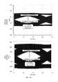
- FIGS. 18, 19, and 20illustrate simulated results of systems with and without high-frequency injection for a 12 mm, 24 mm, and 70 mm channel, respectively.
- FIG. 1illustrates a communication system in accordance with some embodiments employing a vector signaling code.
- Source data to transmitter 110herein illustrated as S 0 , S 1 , S 2 , S 3 , S 4 enters as a source data word 100 into encoder 112 .
- the size of the source data wordmay vary and depends on the parameters of the vector signaling code.
- the encoder 112generates a codeword of the vector signaling code for which the system is designed. In operation, the codeword produced by encoder 112 is used to control PMOS and NMOS transistors within driver 118 , generating two, three, or more distinct voltages or currents on each of the N communication wires 125 of communications channel 120 , to represent the N symbols of the codeword.
- FIG. 1illustrates a communication system in accordance with some embodiments employing a vector signaling code.
- the size of the source data wordis shown as five bits and the codeword size is six symbols.
- communications channel 110is shown as being comprised of six signal wires 125 , each transporting one codeword symbol.
- One familiar with the encoding artsmay also describe this code as having a block length of six (i.e. producing an output word of six symbols) and a code size of 32 (i.e. having 32 distinct codewords, sufficient to encode 5 binary bits of data.)
- detector 132reads the voltages or currents on wires 125 , possibly including amplification, frequency compensation, and common mode signal cancellation.
- the received results 140herein shown as R 0 , R 1 , R 2 , R 3 , R 4 , are provided directly by detector 132 , without need of optional decoder 138 .
- FIG. 1illustrates a system using an ODVS code capable of encoding five binary bit values for transmission over six wires, a so-called 5b6w code.
- the operation of the communications transmitter 110 and communications receiver 130have to be completely synchronized in order to guarantee correct functioning of the communication system.
- this synchronizationis performed by an external clock shared between the transmitter and the receiver.
- Other embodimentsmay combine the clock function with one or more of the data channels, as in the well-known Biphase encoding used for serial communications, or other methods described herein.
- Cronie I, Cronie II, and Holden IIdescribe methods of detecting the symbols that have been sent on a vector signaling link. This disclosure describes several additional methods.
- Holden Ia detection mechanism called maximum-likelihood decoding for use where permutation modulation coding is used for chip-to-chip communication.
- Holden IIteaches a decoder using comparators that compare signal values on two communication wires, producing results that inform sorting or ranking actions within such decoder.
- Such comparatorsare called “simple comparators” hereinafter.
- the number of simple comparators neededis n*(n ⁇ 1)/2, the number of all un-ordered pairs of integers in the range 1, 2, . . . , n. In some applications this number may be too large. For example, where n is 10, the number of simple comparators used is 45, which may be too large to permit implementation in a given application.
- a multi-input comparator with coefficients(also referred to as input weighting factors) a 0 , a 1 , . . . , a m-1 is a circuit that accepts as its input a vector (x 0 , x 1 , . . . , x m-1 and outputs sign( a 0 *x 0 + . . . +a m-1 *x m-1 ), (Eqn. 1)
- a simple comparatormay be seen to be a two input multi-input comparator with coefficients 1 and ⁇ 1, hence may be considered to be a special case of a multi-input comparator.
- the coefficients of a multi-input comparatorare integers.
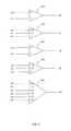
- one circuit implementation of a multi-input comparatoris given with reference to FIG. 2A , showing coefficients of 2, 4, ⁇ 1, ⁇ 2, ⁇ 3 for the input values x 0 through x 4 respectively.
- each of the twelve input transistors 201are identical, representing an extended differential input stage sharing current source 202 , followed by differential comparator stage 205 .
- the contributions of inputs x 0 and x 1 to positive summing node 203 , and of inputs x 2 , x 3 , and x 4 to negative summing node 204are weighted in proportion to the number of input transistors controlled by each such input.
- Resistors 206are shown as passive pull-ups on summing nodes 203 and 204 ; in some embodiments their function will be incorporated in that of differential comparator 205 . Assuming sufficiently high gain in differential comparator 205 to obtain a digital result, its output represents the sign( ) operation taken on the difference between positive summing node 203 and negative summing node 204 .
- the circuit of FIG. 2Aimplements Eqn.
- FIG. 2BAnother multi-input comparator also having the same coefficients is illustrated using a simplified notation in FIG. 2B , where for every input the multiplicity of that input in terms of transistors is a given as a number adjacent to the corresponding transistor.
- such multiple paralleled transistors for the same inputmay be implemented as single transistors having an equivalently scaled channel width, transfer current, or comparable functional characteristics as such multiple paralleled transistors.
- Another embodimentproduces equivalent results dynamically, with inputs controlling the amount of charge on capacitors scaled in proportion to input weights, which are then discharged into a summing node.
- a multi-input comparatoris common mode resistant if the sum of all its coefficients is zero. It is easy to see that if a multi-input comparator is common mode resistant, then simultaneously increasing the values of its inputs by the same amount will not result in any change of the output of the multi-input comparator.
- Multi-input comparatorsmay be susceptible to more thermal noise than simple comparators. If the inputs of a multi-input comparator are independently changed by additive white Gaussian noise of mean 0 and variance ⁇ 2 , the output of the comparator is perturbed by additive white Gaussian noise of mean 0 and variance ⁇ 2 ( a 0 2 + . . . +a m-1 2 ) (Eqn. 2)
- the error probability of this multi-input comparatoris Q ⁇ (a), wherein Q ⁇ (x) is the probability that a normal random variable of mean 0 and variance ⁇ 2 has a value larger than or equal to x.
- sensitivitywe call a the “sensitivity” of the multi-input comparator with respect to its input. Note that by definition sensitivity is nonzero, i.e. if the input of a multi-input comparator is such that the value a as defined in Eqn. 3 is zero, then the sensitivity of the comparator with respect to that particular input is “undefined.”
- a set S of multi-input comparatorsis said to “detect” a vector signaling code C if the following holds: For any two codewords c and d, there is a multi-input comparator in the set S such that the value of that comparator on both c and d is not undefined, and the values are different. This means that the codewords of the vector signaling code are uniquely determined by the outputs of all the multi-input comparators in S when the codeword is used as the input. If a set S of multi-input comparators detects the vector signaling code C, then we define the “minimum sensitivity” of S with respect to C as the minimum sensitivity of any of the comparators applied to any of the codewords, provided that the sensitivity is defined. The notion of minimum sensitivity stands for the maximum amount of thermal noise that can be applied to the codewords while guaranteeing a given detection error probability. Several examples below will illustrate this notion.
- the output of the MICSmay not be sliced using a simple two input comparator, rather a differential output voltage may be provided.
- FIGS. 3A and 3Bdepicts schematics of MICS with and without EQ, respectively, in accordance with such embodiments.
- the MIC with EQ of FIG. 3Aincludes a frequency-selective impedance connecting the sources of all the transistors.
- the frequency-selective impedanceincludes a tunable resistor and a tunable capacitor.
- the frequency-selective impedancemay be used to tune the bandwidth of the MIC.
- the weights applied to the MICS shown in FIGS. 3A and 3Bcorrespond to row 3 of the matrix shown below in Eqn. 4.
- the set of multi-input comparators comprising a code receivermay be concisely described using matrix notation, with the columns of the matrix corresponding to consecutive elements of input vector (x 0 , x 1 , . . . , x m-1 ) i.e. the plurality of signal conductor or wire inputs carrying the vector signaling code, and each row of the matrix corresponding to the vector defining a particular multi-input comparator and its output.
- the value of matrix elementcorresponds to the weight vector or set of scaling factors applied to that column's input values by that row's multi-input comparator.
- the matrix of Eqn. 4describes one such set of multi-input comparators comprising a code receiver.
- the first matrix rowis composed of all “1” values, creating a square 6 ⁇ 6 matrix.
- the matrix described by Eqn. 4will herein be referred to as a Glasswing Receiver matrix.
- Matrix Mmay be normalized to satisfy the stronger conventional orthogonality requirement, but as will subsequently be described such normalization is neither necessary nor desirable in practice.
- orthogonalityrequires that the vector of weights in a row representing a multi-input comparator be orthogonal to all other rows, and that each row representing a multi-input comparator sums to zero (since it is orthogonal to the common mode all 1's codeword).
- the comparator outputsare also orthogonal (and therefore independent,) they represent distinct communications modes, herein described as “sub-channels” of the Vector Signaling Code communications system.
- the initial row of the matrixmay be seen to represent the common-mode communications channel over the transmission medium.
- the first rowis set to all “1” values, maximizing the common mode contribution of each wire input to this one matrix row.
- all rows of the matrixare orthogonal, it follows that no other matrix row (i.e. no receiver output) may then be impacted by common mode signals.
- Embodiments having such common mode rejectionneed not implement a physical comparator corresponding to the first row of their descriptive matrix.
- ODVS sub-channelsare not limited by the example embodiment to a particular ODVS code, transmitter embodiment, or receiver embodiment. Encoders and/or decoders maintaining internal state may also be components of some embodiments. Sub-channels may be represented by individual signals, or by states communicated by multiple signals.
- an Orthogonal Differential Vector Signaling codemay be constructed from a generator matrix by multiplication of an input modulation vector of the form (0, a 1 , a2, . . . a n ) by the matrix M.
- each a i of this vectoris the positive or negative of a single value, as example ⁇ 1, representing one bit of transmitted information.
- multiplication of the matrix by such an input vectorcomprises excitation of the various modes by the a1, of that vector, with the zeroth mode corresponding to common mode transmission not being excited at all. It will be obvious to one familiar with the art that transmission energy emitted in the common mode is both unnecessary and wasteful in most embodiments. However, in at least one embodiment, a nonzero amplitude for the common mode term is used to provide a nonzero bias or baseline value across the communications channel.
- the various codewords of the code generated using this methodrepresent linear combinations of the various orthogonal communication modes. Without additional constraints being imposed (e.g., for purposes of implementation expediency,) this method results in systems capable of communicating N ⁇ 1 distinct sub-channels over N wires, typically embodied as a N ⁇ 1 bit/N wire system.
- the set of discrete codeword values needed to represent the encoded valuesis called the alphabet of the code, and the number of such discrete alphabet values is its alphabet size.
- the alphabet of this codeconsists of the values +1, +1 ⁇ 3, ⁇ 1 ⁇ 3, 1, thus this is a quaternary code (e.g. having an alphabet size of four.)
- This codewill subsequently be described herein as the 5b6w or “Glasswing” code, and its corresponding receive matrix of Eqn. 4 as the “Glasswing receiver”.
- FIG. 4An embodiment of the Glasswing receiver as defined by the matrix of Eqn. 4 is shown in FIG. 4 .
- the six input wiresare w 0 through w 5
- the five sub-channel outputsare S 0 through S 5 .
- each of the inputs of the multiple-input comparators 410 through 450are identified by a weight, representing the relative contribution of that input to the final result output, as defined by the matrix rows of Eqn. 4 defining each MIC.
- 410 and 430may be seen to be conventional dual input differential comparators, each having one positive and one negative input of equal and opposite weight.
- Comparators 420 and 440each have two positive inputs each contributing one half to the total positive value, and one input contributing the entire negative value.
- Comparator 450has three inputs each contributing one third to the total positive value, and three inputs each contributing one third to the total negative value.
- the 5 subchannel outputs S 0 -S 4are denoted with a single line, it should be noted that in many embodiments, each subchannel output may be a differential output.
- FIG. 5depicts a block diagram of an embodiment using a BW-tunable MIC 520 , connected to a voltage sampler driver and amplifier stage (also referred to as the sampler/equalizer) 530 , in accordance with some embodiments.
- a voltage sampler driver and amplifier stagealso referred to as the sampler/equalizer
- Such a designoffers various advantages.
- power dissipation of the CTLEremains fixed even if the channel characteristics are good.
- the sampler/equalizer circuitprovides a degree of freedom such that the apparatus may consume less power when the channel characteristics are good.
- both equalization and power dissipationmay be calibrated based on channel loss. This is something very challenging to do with the conventional architectures.
- an extra CTLE stagemay need to be switched in/out based on the particular channel response, which may be challenging.
- Architectures described herein that utilize a separate BW-tunable MIC 520provide adjustable power dissipation and equalization in a straightforward manner.
- an architecturecomprises a BW-tunable MIC 520 followed by the proposed equalizer/sampler 530 .
- tuning the BW of a CTLE or MICincludes adjusting the frequency-selective impedance and the magnitude of the tail source current.
- calibrating the equalizationincludes adjusting the BW of the MIC without touching the equalizer/sampler stage.
- BWand hence the bias current
- the effective peaking of the pathMIC/equalizer/sampler
- FIG. 13depicts a schematic of an amplifier with a tunable BW.
- the amplifierincludes tunable load impedances 1310 (R L ), a load capacitor C L a tunable current source I SS .
- R Ltunable load impedances 1310
- C Lload capacitor
- I SStunable current source
- R L ⁇ I SSmay be fixed, and the BW may be adjusted by changing R L and I SS inversely (i.e. as R L is increased, I SS is decreased, and vice versa). This will keep the gain constant while tuning BW.
- power consumptionmay be adjusted.
- a low power consumption amplifiermay be designed by increasing R L while decreasing I SS , at the cost of a reduced BW.
- FIG. 14An example schematic of a possible tunable R L is shown in FIG. 14 . As shown, FIG. 14 includes multiple resistors R 1 , R 2 , R 3 , . . . , R n in parallel, each having a series-connected PMOS FETs.
- each resistormay be equal, however this should not be considered limiting.
- each PMOSreceives a corresponding gate input that may connect the corresponding resistor to the V DD common node.
- the control signalsmay be configured (e.g., via a register) to disconnect one or more resistors from the V DD common node.
- known resistance values for given combinations of the control signalsmay be known, and using firmware or a look-up table (LUT), the controls can be provided to the PMOS devices based on a desired load resistance.
- the same controlsmay be used in inversely controlling the magnitude of the tunable current source.
- the differential amplifier configurationis in no way limiting, and that such configurations would work with MICS as well (such as the MICS of FIGS. 3A and 3B , or the MIC with tunable BW 520 shown in FIG. 5 ).
- tunable load impedance 1310does not have to have the configuration shown in FIG. 14 , as tunable load impedance 1310 may include a potentiometer, or any other tunable impedance elements known to those of skill in the art.
- the load capacitor C Lis tunable to provide additional BW tuning while keeping power consumption constant.
- the amplifier with tunable BW shown in FIG. 13is depicted as a differential amplifier, however in some embodiments, the same principles may be implemented in a MIC (such as those depicted in FIGS. 3A and 3B ) to create BW-tunable MIC 520 .
- FIG. 6depicts block diagram including sampler 620 , which includes amplifier stage 630 and voltage sampler driver 640 .
- MIC 420receives a set of input signals w0-w2.
- MIC 420provides a differential voltage +/ ⁇ VIN to voltage sampler driver 640 .
- voltage sampler driveralso receives a clock signal in order to periodically enable the voltage sampler driver.
- the voltage sampler driver 640is configured to draw a differential current through amplifier stage 630 .
- amplifier stage 630includes an integrator with positive feedback.
- amplifier stage 630may include a double-tail latch, as shown in FIG. 15 .
- amplifier stage 630may include a StrongARM latch, as shown in FIG.
- the StrongARM latchoperates in three phases.
- the CLK signalis low, the capacitances CL at nodes Outn, Outp, and the capacitances of M 1 and M 2 are charged to VDD.
- CLKgoes high, and current begins flowing through transistors M 1 and M 2 , and the capacitances of M 1 and M 2 begin discharging.
- the current flowing through the transistors(and therefore the speed at which the capacitances of M 1 and M 2 discharge) is proportional to the inputs INN and INP.
- the cross-coupled transistors M 3 and M 4turn on and CL at nodes Outn and Outp begin to discharge as current through M 3 and M 4 .
- the CL's discharges fastereither PMOS' M 7 and M 5 will turn on (if Outp discharges faster) or PMOS' M 6 and M 8 will discharge (if Outn discharges faster), charging their respective nodes back to VDD, which will increase the rate at which current discharges through the corresponding cross-coupled NMOS M 4 /M 3 , respectively.
- Thiscauses a cascading latch effect to drive Outn and Outp in opposite directions, and the speed at which this process occurs is directly proportional to inputs INN and INP.
- FIG. 16also includes an offset correction differential pair 645 with high-frequency injection connected in parallel to the input differential pair.
- voltage sampler driver 640is configured to draw differential current through the integrator in order to provide a differential voltage output +/ ⁇ VOUT.
- amplifier stage 630includes load resistors to provide the differential output voltage.
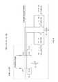
- FIG. 7depicts a diagram of an apparatus, in accordance with some embodiments.
- the apparatusincludes voltage sampler driver 640 configured to generate an output differential current from at least a first differential current and a second differential current, the voltage sampler driver including an input differential branch pair configured to receive a set of input signals +/ ⁇ VIN, each branch of the differential branch pair including one or more transistors for generating the first differential current.
- the voltage sampler driver 640further includes an offset voltage branch pair configured to receive an offset voltage control signal +/ ⁇ VOC, each branch of the offset differential branch pair including one or more transistors for generating the second differential current.
- the 7also includes an amplifier stage 630 connected to the voltage sampler driver 640 , the amplifier stage 630 configured to generate a differential output voltage +/ ⁇ VOUT based on the output differential current drawn by periodically enabling the input differential branch pair and the offset differential branch pair.
- the apparatusfurther includes a high-pass filter for supplementing a high-frequency component of the second differential current by injecting a high-pass filtered version of the set of input signals via the offset differential branch pair.
- the input differential branch pair and the offset differential branch pairare periodically enabled using respective tail current sources (shown as transistors).
- the tail current sourcesare enabled using an input clock signal CK.
- the magnitude of the current drawn through the respective tail current sourcesis independently tunable (by adjusting transistor characteristics, etc.) to allow tuning the frequency-peaking characteristics of the sampler.
- the presence of the offset differential branch pairfacilitates input offset compensation versus, as one example, the capacitive trimming performed to provide offset correction in the latch of [Razavi]. Utilization of the offset differential branch pair to provide additional high-frequency gain further distinguishes such embodiments.
- the current ratio between input differential pairs and the offset correction paircan be adjusted to change the DC gain while high frequency gain remains unchanged.
- the offset differential branch pairmay be incorporated into a MIC, as shown in FIG. 8 .
- the set of input signals received by the input differential branch pair of the MICcorrespond to symbols of a codeword of a vector signaling code.
- a first branch of the input differential branch pairreceives symbols on wires w 0 and w 1
- a second branch of the input differential branch pairreceives symbols on wire w 2 .
- the offset differential branch pairincludes a same transistor configuration as the input differential branch pair.
- the input differential branch pair and the offset differential branch paireach comprises a pair of transistors.
- the input differential branch pair and the offset differential branch paireach include one or more transistors.
- each input signal in the input differential branch pair and the offset differential branch pairhave weights applied to them (as shown in FIGS. 2A and 2B ).
- the weightsare selected according to a row of an orthogonal matrix (e.g., in FIG. 8 , the weights correspond to row 3 of Eqn. 4).
- the weight of a given input signalis determined by a number of identical transistors receiving the same input signal (e.g., a weight of 2 as shown in FIG. 8 is represented as two identical transistors, each receiving w 2 as an input).
- the weight applied to a given input signalis determined by a single transistor having an input weighting factor associated with it.
- the input weighting factormay be determined by transistor characteristics.
- FIG. 9depicts a method 900 , in accordance with some embodiments.
- method 900includes receiving, at step 902 , a set of input signals at an input differential branch pair, and responsively generating a first differential current at step 904 .
- an offset voltage branch pairreceives an offset voltage control signal at an input, and responsively generates a second differential current at step 908 .
- a high-pass filtersupplements a high-frequency component of the second differential current by injecting a high-pass filtered version of the set of input signals into the input of the offset voltage branch pair.
- an amplifier stage connected to the input differential branch pair and the offset voltage branch pairgenerates an output differential current based on the first and second differential currents.
- the steps in FIG. 9are not in any particular order, and that some steps may occur simultaneously.
- the first and second currentsmay be generated simultaneously by receiving the set of input signals at the input differential branch pair, and simultaneously receiving the offset voltage control signal and high-frequency version of the input signals at the input of the offset voltage branch pair.
- the first and second differential currentsare then in effect superimposed on each other to form the output differential current.
- generating the first and second differential currentsincludes enabling corresponding tail current sources for the input differential branch pair and the offset differential branch pair. In some embodiments, the method further includes periodically enabling the respective tail current sources using an input clock signal.
- the methodfurther includes generating a differential output voltage by drawing the output differential current through a pair of load resistors.
- each load resistorhas a corresponding capacitor connected between one terminal of the load resistor and ground.
- the load resistorsare tunable.
- the amplifier stagefurther comprises an adjustable current tail source.
- a product of a current magnitude of the adjustable current tail source and an impedance magnitude of one of the load resistorsis constant, and the method further includes adjusting the pair of load resistors and the tunable current source to adjust bandwidth.
- a product of a current magnitude of the tunable current tail source and an impedance magnitude of one of the load resistorsis not constant, and the method further includes adjusting the pair of load resistors and the current source to adjust power consumption.
- each tunable load resistorcomprises a plurality of resistors in a parallel network
- the methodfurther includes selectably enabling each resistor of the plurality of resistors according to a corresponding switch receiving a corresponding control signal.
- FIG. 10depicts an example configuration (similar to FIG. 8 ) of a MIC/Offset voltage correction combination.
- FIG. 10includes a MIC/Input stage and an Offset Voltage Stage.
- the MIC/Input stageincludes transistors (shown with input weighting factors for simplicity, however this is not limiting), load impedances and a current source with a clock (CK) input.
- FIG. 10also includes an offset voltage stage similar to the offset voltage stage on the right side of FIG. 7 , however there are more than two inputs entering the offset voltage stage.
- the offset voltage stage shown in FIG. 10is utilizing a similar advantage shown in the MIC/Input stage of having a single transistor on the right side with a 2x input weighting factor/coefficient.
- the transistor input weighting factoris implemented by adjusting physical characteristics of the transistor (e.g., channel width).
- the input weighting factoris implemented using a number of identical transistors in parallel, each transistor in parallel receiving the same input.
- FIG. 11depicts a similar embodiment to that of FIG. 10 , however the left side of the offset voltage stage is sharing a transistor with a 2 ⁇ input weighting factor, and the transistor is receiving high frequency content of signals w0 and w1.
- the embodiments shown in FIGS. 10 and 11may be chosen based on design parameters such as device matching (e.g., parasitic input caps and physical caps).
- FIG. 12depicts a combination of the embodiments shown in FIGS. 10 and 11 , which may provide an advantage of having a smaller number of transistors.
- the embodiments shown in FIGS. 10, 11 and 12depict MICS without any equalization or tunable bandwidth, however it should be noted that the EQ technique shown in FIG. 3A and BW tuning technique shown in FIGS. 13 and 14 may be utilized in any of the embodiments shown in FIGS. 10, 11 and 12 .
- FIG. 17depicts a schematic in accordance with some embodiments.
- the circuitincludes a MIC 1705 , a DAC (to provide an offset correction voltage) 1710 , an RC network, an offset correction pair 1715 , an input differential pair 1720 , and a summation node 1725 .
- MIC 1705may take the form of MICS described above.
- the RC networkcorresponds to the RC network of FIG. 7 to inject a high-pass filtered version of the MIC output into the differential current.
- the input differential pair 1720(also referred to as the sampler differential pair) is configured to receive the differential output of MIC 1705 .
- summation nodecorresponds to a junction of wires in order to provide a summation of currents from input differential pair 1720 and offset correction differential pair 1715 .
- FIGS. 18, 19, and 20illustrate simulated results of a given subchannel (Subch 4 ) for a 12 mm, 24 mm and 80 mm channel, respectively.
- the cutoff frequency for the high-pass filteris represented by Eqn. 6 below:
- Cinis the input capacitance of the offset correction differential pair.
- Interpreting a set of signals as selecting an objectcan include selecting the object based at least in part on the set of signals and/or one or more attributes of the set of signals.
- Interpreting a set of signals as representing an objectcan include determining and/or selecting the object based at least in part on a representation corresponding to the set of signals.
- a same set of signalsmay be used to select and/or determine multiple distinct objects (e.g., data objects).
Landscapes
- Engineering & Computer Science (AREA)
- Power Engineering (AREA)
- Computer Networks & Wireless Communication (AREA)
- Signal Processing (AREA)
- Amplifiers (AREA)
Abstract
Description
This application claims priority to US Provisional Patent Application 62/286,717, filed Jan. 25, 2016, naming Armin Tajalli, entitled “Voltage Sampler Driver with Enhanced High-Frequency Gain,” which is herein incorporated by reference in its entirety for all purposes.
The following references are herein incorporated by reference in their entirety for all purposes:
U.S. Patent Publication 2011/0268225 of U.S. patent application Ser. No. 12/784,414, filed May 20, 2010, naming Harm Cronie and Amin Shokrollahi, entitled “Orthogonal Differential Vector Signaling” (hereinafter “Cronie I”);
U.S. Patent Publication 2011/0302478 of U.S. patent application Ser. No. 12/982,777, filed Dec. 30, 2010, naming Harm Cronie and Amin Shokrollahi, entitled “Power and Pin Efficient Chip-to-Chip Communications with Common-Mode Resilience and SSO Resilience” (hereinafter “Cronie II”);
U.S. Patent Publication 2012/0213229, of U.S. patent application Ser. No. 13/030,027, filed Feb. 17, 2011, naming Harm Cronie, Amin Shokrollahi and Armin Tajalli, entitled “Methods and Systems for Noise Resilient, Pin-Efficient and Low Power Communications with Sparse Signaling Codes” (hereinafter “Cronie III”); and
U.S. Pat. No. 8,718,814, issued May 6, 2014 of U.S. patent application Ser. No. 13/463,742, filed May 3, 2012, naming Harm Cronie and Amin Shokrollahi, entitled “Finite State Encoders and Decoders for Vector Signaling Codes” (hereafter called “Cronie IV”).
U.S. Pat. No. 9,300,503, issued Mar. 29, 2016 of U.S. patent application Ser. No. 13/842,740, filed Mar. 15, 2013, naming Brian Holden, Amin Shokrollahi and Anant Singh, entitled “Methods and Systems for Skew Tolerance in and Advanced Detectors for Vector Signaling Codes for Chip-to-Chip Communication”, (hereinafter identified as “Holden I”);
U.S. Pat. No. 9,077,386, issued Jul. 7, 2015 of U.S. patent application Ser. No. 13/603,107, filed Sep. 9, 2012, naming Brian Holden and Amin Shokrollahi, entitled “Methods and Systems for Selection of Unions of Vector Signaling Codes for Power and Pin Efficient Chip-To-Chip Communication” (hereinafter called “Holden II”).
U.S. Pat. No. 8,989,317, issued Mar. 24, 2015 of U.S. patent application Ser. No. 13/671,426, filed Nov. 7, 2012, naming Brian Holden and Amin Shokrollahi, entitled “Crossbar Switch Decoder for Vector Signaling Codes” (hereinafter called “Holden III”).
U.S. Provisional Patent Application 61/839,360, filed Jun. 23, 2013, naming Amin Shokrollahi, entitled “Vector Signaling with Reduced Receiver Complexity” (hereinafter “Shokrollahi I”);
U.S. Provisional Patent Application No. 61/839,360, filed Jun. 23, 2013, naming Amin Shokrollahi, entitled “Vector Signaling Codes with Reduced Receiver Complexity”, hereinafter identified as [Shokrollahi II].
U.S. Provisional Patent Application No. 61/946,574, filed Feb. 28, 2014, naming Amin Shokrollahi, Brian Holden, and Richard Simpson, entitled “Clock Embedded Vector Signaling Codes”, hereinafter identified as [Shokrollahi III].
U.S. Pat. No. 9,288,082, issued Mar. 15, 2016 of U.S. patent application Ser. No. 13/895,206, filed May 15, 2013, naming Roger Ulrich and Peter Hunt, entitled “Circuits for Efficient Detection of Vector Signaling Codes for Chip-to-Chip Communications using Sums of Differences”, hereinafter identified as [Ulrich I].
The following additional references to prior art have been cited in this application:
“The StrongARM Latch, Behzad Razavi“,” IEEE Solid-State Circuits Magazine, Spring 2015, pp. 12-17, DOI 10.1109/MSSC2015.2418155, hereinafter identified as [Razavi].
“A Double-Tail Latch-Type Voltage Sense Amplifier with 18 ps Setup+Hold Time,” Analog Techniques and PLLs, Feb. 13, 2007, pp 314-315, 605, hereinafter identified as [Schinkel].
In communication systems, information may be transmitted from one physical location to another. Furthermore, it is typically desirable that the transport of this information is reliable, is fast and consumes a minimal amount of resources. One of the most common information transfer mediums is the serial communications link, which may be based on a single wire circuit relative to ground or other common reference, multiple such circuits relative to ground or other common reference, or multiple circuits used in relation to each other. An example of the latter utilizes differential signaling (DS). Differential signaling operates by sending a signal on one wire and the opposite of that signal on a paired wire; the signal information is represented by the difference between the wires rather than their absolute values relative to ground or other fixed reference.
Differential signaling enhances the recoverability of the original signal at the receiver, over single ended signaling (SES), by cancelling crosstalk and other common-mode noise, but a side benefit of the technique is that the Simultaneous Switching Noise (SSN) transients generated by the two signals together is nearly zero; if both outputs are presented with an identical load, the transmit demand on its power supply will be constant, regardless of the data being sent. Any induced currents produced by terminating the differential lines in the receiver will similarly cancel out, minimizing noise induction into the receiving system.
There are a number of signaling methods that maintain the desirable properties of DS while increasing pin-efficiency over DS. Many of these attempts operate on more than two wires simultaneously, using binary signals on each wire, but mapping information in groups of bits.
Vector signaling is a method of signaling. With vector signaling, pluralities of signals on a plurality of wires are considered collectively although each of the plurality of signals may be independent. Each of the collective signals is referred to as a component and the number of plurality of wires is referred to as the “dimension” of the vector. In some embodiments, the signal on one wire is entirely dependent on the signal on another wire, as is the case with DS pairs, so in some cases the dimension of the vector may refer to the number of degrees of freedom of signals on the plurality of wires instead of the number of wires in the plurality of wires.
With binary vector signaling, each component takes on a coordinate value (or “coordinate”, for short) that is one of two possible values. As an example, eight SES wires may be considered collectively, with each component/wire taking on one of two values each signal period. A “code word” of this binary vector signaling is one of the possible states of that collective set of components/wires. A “vector signaling code” or “vector signaling vector set” is the collection of valid possible code words for a given vector signaling encoding scheme. A “binary vector signaling code” refers to a mapping and/or set of rules to map information bits to binary vectors.
With non-binary vector signaling, each component has a coordinate value that is a selection from a set of more than two possible values. A “non-binary vector signaling code” refers to a mapping and/or set of rules to map information bits to non-binary vectors.
Examples of vector signaling methods are described in Cronie I, Cronie II, Cronie III, and Cronie IV.
While non-binary vector signaling methods can provide substantial improvements regarding the tradeoff of pin-efficiency, power efficiency and noise resilience as compared to traditional signaling methods, there are some applications wherein additional improvements are possible.
Methods and systems are described for an apparatus including a voltage sampler driver for generating an output differential current from at least a first and a second differential current, the voltage sampler driver including an input differential branch pair for receiving a set of input signals, each branch of the differential branch pair including one or more transistors for generating the first differential current and an offset voltage branch pair for receiving, at an input, an offset voltage control signal, each branch of the offset differential branch pair including one or more transistors for generating the second differential current. The apparatus further includes an amplifier stage connected to the voltage sampler driver, the amplifier stage for generating a differential output voltage based on the output differential current, and a high-pass filter for supplementing a high-frequency component of the second differential current by injecting a high-pass filtered version of the set of input signals into the input of the offset voltage branch pair.
In some embodiments, the voltage sampler driver further includes respective tail current sources, the respective tail current sources periodically enabling the input differential branch pair and offset differential branch pair. In some embodiments, the respective tail current sources are periodically enabled according to an input clock signal. In some embodiments, current magnitudes of the respective tail current sources are independently tunable.
In some embodiments, the amplification stage includes a pair of load resistors for generating a differential output voltage based on the differential current drawn.
In some embodiments, the amplification stage includes an active device. In some embodiments, the active device is a MOS device. In some embodiments, the MOS device is periodically enabled to implement a discrete time domain integrator.
In some embodiments, the set of input signals correspond to symbols of a codeword of an orthogonal-differential vector signaling code (ODVS). In some embodiments, the set of input signals correspond to symbols of a codeword of a permutation modulation (PM) code.
In some embodiments, a first branch of the input differential branch pair comprises at least two transistors connected in parallel. In some embodiments, a first branch of the offset voltage branch pair comprises a number of transistors equal to a number of transistors in the first branch of the input differential branch pair.
In some embodiments, each branch of the input differential branch pair and each branch of the offset correction branch pair comprise a single transistor. In some embodiments, each transistor in the input differential branch pair and the offset voltage branch pair has a weight associated with transistor characteristics. In some embodiments, each weight is determined by a corresponding value of a row of an orthogonal matrix.
In some embodiments, the input differential branch pair comprises a frequency-selective impedance connected at a common node connecting the pair of branches in the input differential branch pair. In some embodiments, the frequency-selective impedance comprises a resistor-capacitor network.
In some embodiments, the apparatus further includes a multi-input comparator (MIC) for providing the set of input signals as a differential input signal. In some embodiments, the input differential signal represents a combination of a plurality of symbols of a codeword.
In some embodiments, the amplifier stage includes an integrator circuit for generating a differential output voltage based on the differential currents. In some embodiments, the integrator is a discrete time integrator with periodically enabled load devices. In some embodiments, a single wire of the differential voltage output represents a single-ended output. In some embodiments, the amplifier is a voltage mode amplifier.
In some embodiments, the apparatus further includes a comparator for forming a single-ended output by slicing the differential voltage output.
In some embodiments, the offset voltage control signal accounts for an offset error introduced by components of the voltage sampler driver and/or the amplifier stage. In some embodiments, the voltage sampler driver includes NMOS transistors. In some embodiments, the voltage sampler driver includes PMOS transistors.
In some embodiments, the offset voltage control signal represents an arbitrary reference voltage.
In some embodiments, the amplifier stage includes a pair of load resistors for generating the differential output voltage based on the output differential current. In some embodiments the amplifier stage further includes a pair of capacitors, each capacitor connected between one terminal of a corresponding load resistor and ground. In some embodiments, the pair of load resistors are tunable. In some embodiments, the amplifier stage further includes an adjustable current tail source.
In some embodiments, a product of a current magnitude of the adjustable current tail source and an impedance magnitude of one of the load resistors is constant, and the pair of load resistors and the tunable current source have a bandwidth control input to adjust bandwidth. In alternative embodiments, a product of a current magnitude of the tunable current tail source and an impedance magnitude of one of the load resistors is not constant, the pair of load resistors and the current source having a power control input to adjust power consumption.
In some embodiments, each tunable load resistor includes a plurality of resistors in a parallel network, each resistor of the plurality having a corresponding switch connected between the resistor and a common node of the parallel network, and wherein each switch connects/disconnects the resistor from the parallel network based on a respective control signal.
This Brief Summary is provided to introduce a selection of concepts in a simplified form that are further described below in the Detailed Description. This Brief Summary is not intended to identify key or essential features of the claimed subject matter, nor is it intended to be used as an aid in determining the scope of the claimed subject matter. Other objects and/or advantages of described embodiments will be apparent to one of ordinary skill in the art upon review of the Detailed Description and the included drawings.
Various embodiments in accordance with the present disclosure will be described with reference to the drawings. Same numbers are used throughout the disclosure and figures to reference like components and features.
Withincommunications receiver 130,detector 132 reads the voltages or currents onwires 125, possibly including amplification, frequency compensation, and common mode signal cancellation. In the present example, the receivedresults 140, herein shown as R0, R1, R2, R3, R4, are provided directly bydetector 132, without need ofoptional decoder 138.
As will be readily apparent, different codes may be associated with different block sizes and different codeword sizes; for descriptive convenience and without implying limitation, the example ofFIG. 1 illustrates a system using an ODVS code capable of encoding five binary bit values for transmission over six wires, a so-called 5b6w code.
Depending on which vector signaling code is used, there may be no decoder, or no encoder, or neither a decoder nor an encoder. For example, for the 8b8w code disclosed in [Cronie II], bothencoder 112 anddecoder 138 exist. On the other hand, for the 5b6w code of the present example, an explicit decoder is unnecessary, as the system may be configured such thatdetector 132 generates the receivedresults 140 directly.
The operation of thecommunications transmitter 110 andcommunications receiver 130 have to be completely synchronized in order to guarantee correct functioning of the communication system. In some embodiments, this synchronization is performed by an external clock shared between the transmitter and the receiver. Other embodiments may combine the clock function with one or more of the data channels, as in the well-known Biphase encoding used for serial communications, or other methods described herein.
Cronie I, Cronie II, and Holden II describe methods of detecting the symbols that have been sent on a vector signaling link. This disclosure describes several additional methods.
As described by Holden I, a detection mechanism called maximum-likelihood decoding for use where permutation modulation coding is used for chip-to-chip communication. Holden II teaches a decoder using comparators that compare signal values on two communication wires, producing results that inform sorting or ranking actions within such decoder.
The operation of such a comparator can be succinctly described using the “sign” notation, given in the following: sign(x)=+1 if x>0, sign(x)=−1 if x<0, and sign(x) is undefined if x=0. That is, if two values entering a comparator are equal, or close to equal, then the value output by the comparator can be a +1 or a −1, and it is not clear a-priori which of these values is output. Such comparators are called “simple comparators” hereinafter.
In some applications, it may be the case that simple comparators are not sufficient to detect the codewords of a vector signaling code. As an example, consider the union of two PM-codes, one generated as permutations of the vector (1,0,0,−1), and one generated as permutations of the vector (1,1,−1,−1). This union contains 18 codewords, whereas each constituent PM-code contains at most 12 codewords, versus the 16 unique codewords needed to represent a four-bit data value. It is therefore not possible to transmit 4 bits on 4 wires using one PM-code alone, whereas with the union of these two PM-codes a full pin-efficient transmission on 4 wires is possible. Such transmission will be feasible if detection of the codewords can be done with efficient circuitry. It is easy to see that even a full set of 6 simple comparators between pairs of wires is not sufficient to detect a codeword, as those comparisons give no information as to which of the two constituent PM-codes include the received word.
In an application where the values on n communication wires need to be ranked, the number of simple comparators needed is n*(n−1)/2, the number of all un-ordered pairs of integers in therange
For these reasons, it is important to devise circuits that can be implemented more efficiently than those requiring unacceptable numbers of simple comparators, as well as enabling detection of codewords that would otherwise be undetectable. Such circuits will be described, using an element that hereinafter is termed a multi-input comparator.
A multi-input comparator with coefficients (also referred to as input weighting factors) a0, a1, . . . , am-1is a circuit that accepts as its input a vector (x0, x1, . . . , xm-1and outputs
sign(a0*x0+ . . . +am-1*xm-1), (Eqn. 1)
sign(a0*x0+ . . . +am-1*xm-1), (Eqn. 1)
with the definition of the sign-function given above. As such, a simple comparator may be seen to be a two input multi-input comparator withcoefficients 1 and −1, hence may be considered to be a special case of a multi-input comparator.
In accordance with at least one embodiment, the coefficients of a multi-input comparator are integers. In such cases, one circuit implementation of a multi-input comparator is given with reference toFIG. 2A , showing coefficients of 2, 4,−1,−2,−3 for the input values x0 through x4 respectively. In this example, each of the twelveinput transistors 201 are identical, representing an extended differential input stage sharingcurrent source 202, followed bydifferential comparator stage 205. As alltransistors 201 are identical, the contributions of inputs x0 and x1 to positive summingnode 203, and of inputs x2, x3, and x4 to negative summingnode 204 are weighted in proportion to the number of input transistors controlled by each such input.Resistors 206 are shown as passive pull-ups on summingnodes differential comparator 205. Assuming sufficiently high gain indifferential comparator 205 to obtain a digital result, its output represents the sign( ) operation taken on the difference between positive summingnode 203 and negative summingnode 204. Thus, the circuit ofFIG. 2A implements Eqn. 1, where inputs with positive coefficients are attached totransistors 201 associated with positive summingnode 203, and inputs with negative coefficients are attached totransistors 201 associated with negative summingnode 204, the coefficient values being represented by the number ofidentical input transistors 201 used for each input.
Another multi-input comparator also having the same coefficients is illustrated using a simplified notation inFIG. 2B , where for every input the multiplicity of that input in terms of transistors is a given as a number adjacent to the corresponding transistor. In accordance with at least one embodiment, such multiple paralleled transistors for the same input may be implemented as single transistors having an equivalently scaled channel width, transfer current, or comparable functional characteristics as such multiple paralleled transistors. Another embodiment produces equivalent results dynamically, with inputs controlling the amount of charge on capacitors scaled in proportion to input weights, which are then discharged into a summing node.
A multi-input comparator is common mode resistant if the sum of all its coefficients is zero. It is easy to see that if a multi-input comparator is common mode resistant, then simultaneously increasing the values of its inputs by the same amount will not result in any change of the output of the multi-input comparator.
Multi-input comparators may be susceptible to more thermal noise than simple comparators. If the inputs of a multi-input comparator are independently changed by additive white Gaussian noise ofmean 0 and variance σ2, the output of the comparator is perturbed by additive white Gaussian noise ofmean 0 and variance
σ2(a02+ . . . +am-12) (Eqn. 2)
σ2(a02+ . . . +am-12) (Eqn. 2)
If, for a given input (x0, x1, x2, . . . , xm-1) and (y0, y1, y2, . . . , yt-1) the value
is nonzero, then the error probability of this multi-input comparator is Qσ(a), wherein Qσ(x) is the probability that a normal random variable of mean 0 and variance σ2has a value larger than or equal to x. Hereinafter we call a the “sensitivity” of the multi-input comparator with respect to its input. Note that by definition sensitivity is nonzero, i.e. if the input of a multi-input comparator is such that the value a as defined in Eqn. 3 is zero, then the sensitivity of the comparator with respect to that particular input is “undefined.”
A set S of multi-input comparators is said to “detect” a vector signaling code C if the following holds: For any two codewords c and d, there is a multi-input comparator in the set S such that the value of that comparator on both c and d is not undefined, and the values are different. This means that the codewords of the vector signaling code are uniquely determined by the outputs of all the multi-input comparators in S when the codeword is used as the input. If a set S of multi-input comparators detects the vector signaling code C, then we define the “minimum sensitivity” of S with respect to C as the minimum sensitivity of any of the comparators applied to any of the codewords, provided that the sensitivity is defined. The notion of minimum sensitivity stands for the maximum amount of thermal noise that can be applied to the codewords while guaranteeing a given detection error probability. Several examples below will illustrate this notion.
In some embodiments, the output of the MICS may not be sliced using a simple two input comparator, rather a differential output voltage may be provided.FIGS. 3A and 3B depicts schematics of MICS with and without EQ, respectively, in accordance with such embodiments. The MIC with EQ ofFIG. 3A includes a frequency-selective impedance connecting the sources of all the transistors. In some embodiments as shown, the frequency-selective impedance includes a tunable resistor and a tunable capacitor. In some embodiments the frequency-selective impedance may be used to tune the bandwidth of the MIC. The weights applied to the MICS shown inFIGS. 3A and 3B correspond to row 3 of the matrix shown below in Eqn. 4.
Receivers Using Multi-Input Comparators
Mathematically, the set of multi-input comparators comprising a code receiver may be concisely described using matrix notation, with the columns of the matrix corresponding to consecutive elements of input vector (x0, x1, . . . , xm-1) i.e. the plurality of signal conductor or wire inputs carrying the vector signaling code, and each row of the matrix corresponding to the vector defining a particular multi-input comparator and its output. In this notation, the value of matrix element corresponds to the weight vector or set of scaling factors applied to that column's input values by that row's multi-input comparator.
The matrix of Eqn. 4 describes one such set of multi-input comparators comprising a code receiver.
In this embodiment, six input wires, represented by the six matrix columns, are processed by five multi-input comparators represented by matrix rows 2-6. For purposes to be subsequently described, the first matrix row is composed of all “1” values, creating a square 6×6 matrix. The matrix described by Eqn. 4 will herein be referred to as a Glasswing Receiver matrix.
As used herein, a matrix M such as that of Eqn. 4 is called “orthogonal” if MTM=D that is, if the product of the matrix and its transpose is a diagonal matrix having non-zero values only on its diagonal. This is a weaker definition than commonly used, where the result is be the identity matrix, i.e. having diagonal values equal to 1. Matrix M may be normalized to satisfy the stronger conventional orthogonality requirement, but as will subsequently be described such normalization is neither necessary nor desirable in practice.
Functionally, orthogonality requires that the vector of weights in a row representing a multi-input comparator be orthogonal to all other rows, and that each row representing a multi-input comparator sums to zero (since it is orthogonal to the common mode all 1's codeword). As this implies the comparator outputs are also orthogonal (and therefore independent,) they represent distinct communications modes, herein described as “sub-channels” of the Vector Signaling Code communications system.
Given this modal interpretation, the initial row of the matrix may be seen to represent the common-mode communications channel over the transmission medium. As it is desirable in a practical system for the receiver to have common-mode rejection, the first row is set to all “1” values, maximizing the common mode contribution of each wire input to this one matrix row. As by definition all rows of the matrix are orthogonal, it follows that no other matrix row (i.e. no receiver output) may then be impacted by common mode signals. Embodiments having such common mode rejection need not implement a physical comparator corresponding to the first row of their descriptive matrix.
For avoidance of confusion, it is noted that all data communications in an ODVS system, including the state changes representing signals carried in sub-channels, are communicated as codewords over the entire channel. An embodiment may associate particular mappings of input values to codewords and correlate those mappings with particular detector results, as taught herein and by [Holden I] and [Ulrich I], but those correlations should not be confused with partitions, sub-divisions, or sub-channels of the physical communications medium itself. Similarly, the concept of ODVS sub-channels is not limited by the example embodiment to a particular ODVS code, transmitter embodiment, or receiver embodiment. Encoders and/or decoders maintaining internal state may also be components of some embodiments. Sub-channels may be represented by individual signals, or by states communicated by multiple signals.
Generating ODVS Codes Corresponding to a Receiver Matrix
As described in [Cronie I] and [Cronie II], an Orthogonal Differential Vector Signaling code may be constructed from a generator matrix by multiplication of an input modulation vector of the form (0, a1, a2, . . . an) by the matrix M. In the simplest case, each aiof this vector is the positive or negative of a single value, as example ±1, representing one bit of transmitted information.
Given the understanding of M as describing the various communications modes of the system, it may readily be seen that multiplication of the matrix by such an input vector comprises excitation of the various modes by the a1, of that vector, with the zeroth mode corresponding to common mode transmission not being excited at all. It will be obvious to one familiar with the art that transmission energy emitted in the common mode is both unnecessary and wasteful in most embodiments. However, in at least one embodiment, a nonzero amplitude for the common mode term is used to provide a nonzero bias or baseline value across the communications channel.
It also may be seen that the various codewords of the code generated using this method represent linear combinations of the various orthogonal communication modes. Without additional constraints being imposed (e.g., for purposes of implementation expediency,) this method results in systems capable of communicating N−1 distinct sub-channels over N wires, typically embodied as a N−1 bit/N wire system. The set of discrete codeword values needed to represent the encoded values is called the alphabet of the code, and the number of such discrete alphabet values is its alphabet size.
As a further example, the code generated by this method from the matrix of Eqn. 4 is shown in Table 1.
| TABLE 1 | |||
| ±[1, ⅓, −⅓, −1, −⅓, ⅓] | ±[1, ⅓, −⅓, ⅓, −1, −⅓] | ||
| ±[⅓, 1, −⅓, −1, −⅓, ⅓] | ±[⅓, 1, −⅓, ⅓, −1, −⅓] | ||
| ±[⅓, −⅓, 1, −1, −⅓, ⅓] | ±[⅓, −⅓, 1, ⅓, −1, −⅓] | ||
| ±[−⅓, ⅓, 1, −1, −⅓, ⅓] | ±[−⅓, ⅓, 1, ⅓, −1, −⅓] | ||
| ±[1, ⅓, −⅓, −1, ⅓, −⅓] | ±[1, ⅓, −⅓, ⅓, −⅓, −1] | ||
| ±[⅓, 1, −⅓, −1, ⅓, −⅓] | ±[⅓, 1, −⅓, ⅓, −⅓, −1] | ||
| ±[⅓, −⅓, 1, −1, ⅓, −⅓] | ±[⅓, −⅓, 1, ⅓, −⅓, −1] | ||
| ±[−⅓, ⅓, 1, −1, ⅓, −⅓] | ±[−⅓, ⅓, 1, ⅓, −⅓, −1] | ||
As may be readily observed, the alphabet of this code consists of the values +1, +⅓,−⅓, 1, thus this is a quaternary code (e.g. having an alphabet size of four.) This code will subsequently be described herein as the 5b6w or “Glasswing” code, and its corresponding receive matrix of Eqn. 4 as the “Glasswing receiver”.
An embodiment of the Glasswing receiver as defined by the matrix of Eqn. 4 is shown inFIG. 4 . The six input wires are w0through w5, and the five sub-channel outputs are S0through S5. In the drawing convention used here, each of the inputs of the multiple-input comparators 410 through450 are identified by a weight, representing the relative contribution of that input to the final result output, as defined by the matrix rows of Eqn. 4 defining each MIC. Thus,410 and430 may be seen to be conventional dual input differential comparators, each having one positive and one negative input of equal and opposite weight.Comparators Comparator 450 has three inputs each contributing one third to the total positive value, and three inputs each contributing one third to the total negative value. Although the 5 subchannel outputs S0-S4 are denoted with a single line, it should be noted that in many embodiments, each subchannel output may be a differential output.
To adjust the BW of the amplifier shown inFIG. 13 , RL·ISSmay be fixed, and the BW may be adjusted by changing RLand ISSinversely (i.e. as RLis increased, ISSis decreased, and vice versa). This will keep the gain constant while tuning BW. In such embodiments, power consumption may be adjusted. A low power consumption amplifier may be designed by increasing RLwhile decreasing ISS, at the cost of a reduced BW. An example schematic of a possible tunable RLis shown inFIG. 14 . As shown,FIG. 14 includes multiple resistors R1, R2, R3, . . . , Rnin parallel, each having a series-connected PMOS FETs. In some embodiments, the values of each resistor may be equal, however this should not be considered limiting. InFIG. 14 , each PMOS receives a corresponding gate input that may connect the corresponding resistor to the VDDcommon node. As will be apparent to one of skill in the art, increasing parallel resistance will lower the overall resistance of the circuit. In order to increase resistance, the control signals may be configured (e.g., via a register) to disconnect one or more resistors from the VDDcommon node. In some embodiments, known resistance values for given combinations of the control signals may be known, and using firmware or a look-up table (LUT), the controls can be provided to the PMOS devices based on a desired load resistance. In some embodiments (constant power embodiments), the same controls may be used in inversely controlling the magnitude of the tunable current source. It should be noted that the differential amplifier configuration is in no way limiting, and that such configurations would work with MICS as well (such as the MICS ofFIGS. 3A and 3B , or the MIC withtunable BW 520 shown inFIG. 5 ). Further, in alternative embodiments,tunable load impedance 1310 does not have to have the configuration shown inFIG. 14 , astunable load impedance 1310 may include a potentiometer, or any other tunable impedance elements known to those of skill in the art. In other alternative embodiments, it may be feasible that the load capacitor CLis tunable to provide additional BW tuning while keeping power consumption constant. It should be noted that the amplifier with tunable BW shown inFIG. 13 is depicted as a differential amplifier, however in some embodiments, the same principles may be implemented in a MIC (such as those depicted inFIGS. 3A and 3B ) to create BW-tunable MIC 520.
In some embodiments, the offset differential branch pair may be incorporated into a MIC, as shown inFIG. 8 . In one embodiment, the set of input signals received by the input differential branch pair of the MIC correspond to symbols of a codeword of a vector signaling code. As shown, a first branch of the input differential branch pair receives symbols on wires w0 and w1, while a second branch of the input differential branch pair receives symbols on wire w2. In some embodiments, as shown, the offset differential branch pair includes a same transistor configuration as the input differential branch pair. In some embodiments, the input differential branch pair and the offset differential branch pair each comprises a pair of transistors. In some embodiments, the input differential branch pair and the offset differential branch pair each include one or more transistors. In some embodiments, each input signal in the input differential branch pair and the offset differential branch pair have weights applied to them (as shown inFIGS. 2A and 2B ). In some embodiments, the weights are selected according to a row of an orthogonal matrix (e.g., inFIG. 8 , the weights correspond to row 3 of Eqn. 4). In some embodiments, the weight of a given input signal is determined by a number of identical transistors receiving the same input signal (e.g., a weight of 2 as shown inFIG. 8 is represented as two identical transistors, each receiving w2 as an input). In some embodiments, the weight applied to a given input signal is determined by a single transistor having an input weighting factor associated with it. In some embodiments, the input weighting factor may be determined by transistor characteristics.
In some embodiments, generating the first and second differential currents includes enabling corresponding tail current sources for the input differential branch pair and the offset differential branch pair. In some embodiments, the method further includes periodically enabling the respective tail current sources using an input clock signal.
In some embodiments, the method further includes generating a differential output voltage by drawing the output differential current through a pair of load resistors. In some embodiments, each load resistor has a corresponding capacitor connected between one terminal of the load resistor and ground. In some embodiments, the load resistors are tunable. In some embodiments, the amplifier stage further comprises an adjustable current tail source.
In some embodiments, a product of a current magnitude of the adjustable current tail source and an impedance magnitude of one of the load resistors is constant, and the method further includes adjusting the pair of load resistors and the tunable current source to adjust bandwidth. Alternatively, a product of a current magnitude of the tunable current tail source and an impedance magnitude of one of the load resistors is not constant, and the method further includes adjusting the pair of load resistors and the current source to adjust power consumption.
In some embodiments, each tunable load resistor comprises a plurality of resistors in a parallel network, and the method further includes selectably enabling each resistor of the plurality of resistors according to a corresponding switch receiving a corresponding control signal.
wherein Cin is the input capacitance of the offset correction differential pair. Typical values may include: Cin=2fF, C=9fF, R=2 k−200 k.
The examples presented herein illustrate the use of vector signaling codes for point-to-point wire communications. However, this should not be seen in any way as limiting the scope of the described embodiments. The methods disclosed in this application are equally applicable to other communication media including optical and wireless communications. Thus, descriptive terms such as “voltage” or “signal level” should be considered to include equivalents in other measurement systems, such as “optical intensity”, “RF modulation”, etc. As used herein, the term “physical signal” includes any suitable behavior and/or attribute of a physical phenomenon capable of conveying information. Physical signals may be tangible and non-transitory.
Interpreting a set of signals as selecting an object (e.g., a data object) can include selecting the object based at least in part on the set of signals and/or one or more attributes of the set of signals. Interpreting a set of signals as representing an object (e.g., a data object) can include determining and/or selecting the object based at least in part on a representation corresponding to the set of signals. A same set of signals may be used to select and/or determine multiple distinct objects (e.g., data objects).
Claims (20)
1. An apparatus comprising:
a voltage sampler driver configured to generate an output differential current from at least a first and a second differential current, the voltage sampler driver comprising:
an input differential branch pair configured to receive a set of input signals, each branch of the differential branch pair comprising one or more transistors configured to generate the first differential current;
an offset voltage branch pair configured to receive, at an input, an offset voltage control signal, each branch of the offset differential branch pair comprising one or more transistors configured to generate the second differential current;
an amplifier stage connected to the voltage sampler driver, the amplifier stage configured to generate a differential output voltage based on the output differential current; and
a high-pass filter configured to supplement a high-frequency component of the second differential current by injecting a high-pass filtered version of the set of input signals into the input of the offset voltage branch pair.
2. The apparatus ofclaim 1 , wherein the voltage sampler driver further comprises respective tail current sources, the respective tail current sources configured to enable the input differential branch pair and offset differential branch pair.
3. The apparatus ofclaim 2 , wherein the respective tail current sources are periodically enabled according to an input clock signal.
4. The apparatus ofclaim 1 , wherein the amplifier stage comprises a pair of load resistors configured to generate the differential output voltage based on the output differential current.
5. The apparatus ofclaim 4 , wherein the amplifier stage further comprises a pair of capacitors, each capacitor connected between one terminal of a corresponding load resistor and ground.
6. The apparatus ofclaim 5 , wherein the pair of load resistors are tunable.
7. The apparatus ofclaim 6 , wherein the amplifier stage further comprises an adjustable tail current source.
8. The apparatus ofclaim 7 , wherein a product of a current magnitude of the adjustable tail current source and an impedance magnitude of one of the load resistors is constant, and wherein the pair of load resistors and the tunable current source have a bandwidth control input to adjust bandwidth.
9. The apparatus ofclaim 7 , wherein a product of a current magnitude of the adjustable tail current source and an impedance magnitude of one of the load resistors is not constant, the pair of load resistors and the adjustable tail current source having a power control input to adjust power consumption.
10. The apparatus ofclaim 6 , wherein each tunable load resistor comprises a plurality of resistors in a parallel network, each resistor of the plurality having a corresponding switch connected between the resistor and a common node of the parallel network, and wherein each switch is configured to connect or disconnect the resistor from the parallel network based on a respective control signal.
11. A method comprising:
receiving, at an input differential branch pair, a set of input signals, and responsively generating a first differential current;
receiving, at an input of an offset voltage branch pair, an offset voltage control signal, and responsively generating a second differential current;
supplementing a high-frequency component of the second differential current by injecting a high-pass filtered version of the set of input signals into the input of the offset voltage branch pair using a high-pass filter; and
generating an output differential current based on the first and second differential currents using an amplifier stage connected to the input differential branch pair and the offset voltage branch pair.
12. The method ofclaim 11 , wherein generating the first and second differential currents comprises enabling corresponding tail current sources for the input differential branch pair and the offset differential branch pair.
13. The method ofclaim 12 , further comprising periodically enabling the respective tail current sources using an input clock signal.
14. The method ofclaim 11 , further comprising generating a differential output voltage by drawing the output differential current through a pair of load resistors.
15. The method ofclaim 14 , wherein each load resistor has a corresponding capacitor connected between one terminal of the load resistor and ground.
16. The method ofclaim 15 , wherein the pair of load resistors are tunable.
17. The method ofclaim 16 , wherein the amplifier stage further comprises an adjustable tail current source.
18. The method ofclaim 17 , wherein a product of a current magnitude of the adjustable tail current source and an impedance magnitude of one of the load resistors is constant, and wherein the method further comprises adjusting the pair of load resistors and the adjustable tail current source to adjust bandwidth.
19. The method ofclaim 17 , wherein a product of a current magnitude of the adjustable tail current source and an impedance magnitude of one of the load resistors is not constant, and wherein the method further comprises adjusting the pair of load resistors and the adjustable tail current source to adjust power consumption.
20. The method ofclaim 16 , wherein each tunable load resistor comprises a plurality of resistors in a parallel network, and wherein the method further comprises selectably enabling each resistor of the plurality of resistors according to a corresponding switch receiving a corresponding control signal.
Priority Applications (3)
| Application Number | Priority Date | Filing Date | Title |
|---|---|---|---|
| US15/415,831US10003315B2 (en) | 2016-01-25 | 2017-01-25 | Voltage sampler driver with enhanced high-frequency gain |
| US16/012,649US10498305B2 (en) | 2016-01-25 | 2018-06-19 | Voltage sampler driver with enhanced high-frequency gain |
| US16/702,260US11183982B2 (en) | 2016-01-25 | 2019-12-03 | Voltage sampler driver with enhanced high-frequency gain |
Applications Claiming Priority (2)
| Application Number | Priority Date | Filing Date | Title |
|---|---|---|---|
| US201662286717P | 2016-01-25 | 2016-01-25 | |
| US15/415,831US10003315B2 (en) | 2016-01-25 | 2017-01-25 | Voltage sampler driver with enhanced high-frequency gain |
Related Child Applications (1)
| Application Number | Title | Priority Date | Filing Date |
|---|---|---|---|
| US16/012,649ContinuationUS10498305B2 (en) | 2016-01-25 | 2018-06-19 | Voltage sampler driver with enhanced high-frequency gain |
Publications (2)
| Publication Number | Publication Date |
|---|---|
| US20170214374A1 US20170214374A1 (en) | 2017-07-27 |
| US10003315B2true US10003315B2 (en) | 2018-06-19 |
Family
ID=59359914
Family Applications (3)
| Application Number | Title | Priority Date | Filing Date |
|---|---|---|---|
| US15/415,831ActiveUS10003315B2 (en) | 2016-01-25 | 2017-01-25 | Voltage sampler driver with enhanced high-frequency gain |
| US16/012,649ActiveUS10498305B2 (en) | 2016-01-25 | 2018-06-19 | Voltage sampler driver with enhanced high-frequency gain |
| US16/702,260Active2037-04-06US11183982B2 (en) | 2016-01-25 | 2019-12-03 | Voltage sampler driver with enhanced high-frequency gain |
Family Applications After (2)
| Application Number | Title | Priority Date | Filing Date |
|---|---|---|---|
| US16/012,649ActiveUS10498305B2 (en) | 2016-01-25 | 2018-06-19 | Voltage sampler driver with enhanced high-frequency gain |
| US16/702,260Active2037-04-06US11183982B2 (en) | 2016-01-25 | 2019-12-03 | Voltage sampler driver with enhanced high-frequency gain |
Country Status (4)
| Country | Link |
|---|---|
| US (3) | US10003315B2 (en) |
| EP (1) | EP3408935B1 (en) |
| CN (1) | CN108781060B (en) |
| WO (1) | WO2017132292A1 (en) |
Cited By (21)
| Publication number | Priority date | Publication date | Assignee | Title |
|---|---|---|---|---|
| US20170317855A1 (en)* | 2016-04-28 | 2017-11-02 | Kandou Labs, S.A. | Vector signaling codes for densely-routed wire groups |
| US10498305B2 (en) | 2016-01-25 | 2019-12-03 | Kandou Labs, S.A. | Voltage sampler driver with enhanced high-frequency gain |
| US10560293B2 (en) | 2010-12-30 | 2020-02-11 | Kandou Labs, S.A. | Circuits for efficient detection of vector signaling codes for chip-to-chip communication |
| US10574487B1 (en) | 2019-04-08 | 2020-02-25 | Kandou Labs, S.A. | Sampler offset calibration during operation |
| US10574370B2 (en) | 2010-12-30 | 2020-02-25 | Kandou Labs, S.A. | Methods and systems for skew tolerance in and advanced detectors for vector signaling codes for chip-to-chip communication |
| US10608849B1 (en) | 2019-04-08 | 2020-03-31 | Kandou Labs, S.A. | Variable gain amplifier and sampler offset calibration without clock recovery |
| US10608847B2 (en) | 2016-10-24 | 2020-03-31 | Kandou Labs, S.A. | Multi-stage sampler with increased gain |
| US10673608B2 (en) | 2016-04-22 | 2020-06-02 | Kandou Labs, S.A. | Sampler with low input kickback |
| US10673548B2 (en) | 2017-12-07 | 2020-06-02 | Kandou Labs, S.A. | Decision feedback equalization correction of eye scope measurements |
| US10679716B2 (en) | 2016-04-22 | 2020-06-09 | Kandou Labs, S.A. | Calibration apparatus and method for sampler with adjustable high frequency gain |
| US10680634B1 (en) | 2019-04-08 | 2020-06-09 | Kandou Labs, S.A. | Dynamic integration time adjustment of a clocked data sampler using a static analog calibration circuit |
| US10721106B1 (en) | 2019-04-08 | 2020-07-21 | Kandou Labs, S.A. | Adaptive continuous time linear equalization and channel bandwidth control |
| US10742451B2 (en) | 2018-06-12 | 2020-08-11 | Kandou Labs, S.A. | Passive multi-input comparator for orthogonal codes on a multi-wire bus |
| US10931249B2 (en) | 2018-06-12 | 2021-02-23 | Kandou Labs, S.A. | Amplifier with adjustable high-frequency gain using varactor diodes |
| US11183983B2 (en) | 2018-09-10 | 2021-11-23 | Kandou Labs, S.A. | Programmable continuous time linear equalizer having stabilized high-frequency peaking for controlling operating current of a slicer |
| US11265140B2 (en) | 2016-04-22 | 2022-03-01 | Kandou Labs, S.A. | High performance phase locked loop |
| US11303484B1 (en) | 2021-04-02 | 2022-04-12 | Kandou Labs SA | Continuous time linear equalization and bandwidth adaptation using asynchronous sampling |
| US11374800B1 (en) | 2021-04-14 | 2022-06-28 | Kandou Labs SA | Continuous time linear equalization and bandwidth adaptation using peak detector |
| US11456708B1 (en) | 2021-04-30 | 2022-09-27 | Kandou Labs SA | Reference generation circuit for maintaining temperature-tracked linearity in amplifier with adjustable high-frequency gain |
| US20230308053A1 (en)* | 2017-12-29 | 2023-09-28 | Texas Instruments Incorporated | Dynamically biased power amplification |
| US12355409B2 (en) | 2022-03-24 | 2025-07-08 | Kandou Labs SA | Variable gain amplifier with cross-coupled common mode reduction |
Families Citing this family (10)
| Publication number | Priority date | Publication date | Assignee | Title |
|---|---|---|---|---|
| US10411922B2 (en) | 2016-09-16 | 2019-09-10 | Kandou Labs, S.A. | Data-driven phase detector element for phase locked loops |
| US11075779B2 (en)* | 2018-03-30 | 2021-07-27 | Intel Corporation | Transceiver baseband processing |
| JP2020088020A (en)* | 2018-11-16 | 2020-06-04 | ソニーセミコンダクタソリューションズ株式会社 | Detection circuit, drive circuit, and light-emitting device |
| WO2020110504A1 (en)* | 2018-11-27 | 2020-06-04 | ソニーセミコンダクタソリューションズ株式会社 | Drive device and light-emitting device |
| KR102679564B1 (en)* | 2019-11-01 | 2024-06-27 | 삼성전자주식회사 | Transmitter circuit, method of data transmission and electronic system |
| US11625054B2 (en)* | 2021-06-17 | 2023-04-11 | Novatek Microelectronics Corp. | Voltage to current converter of improved size and accuracy |
| US11962440B2 (en)* | 2021-12-14 | 2024-04-16 | Qualcomm Incorporated | Decision feedback equalizer for low-voltage high-speed serial links |
| KR102652748B1 (en)* | 2022-01-27 | 2024-03-29 | 주식회사 유니컨 | Differential envelope detector with common mode feedback |
| US12021669B2 (en) | 2022-11-11 | 2024-06-25 | Qualcomm Incorporated | Clocked comparator with series decision feedback equalization |
| US20250267047A1 (en)* | 2024-02-20 | 2025-08-21 | Qualcomm Incorporated | Sampler input calibration in a serdes receiver using a self-generated reference voltage |
Citations (333)
| Publication number | Priority date | Publication date | Assignee | Title |
|---|---|---|---|---|
| US668687A (en) | 1900-12-06 | 1901-02-26 | Louis G Mayer | Thill-coupling. |
| US780883A (en) | 1903-11-18 | 1905-01-24 | Mortimer Livingston Hinchman | Advertising device. |
| US3196351A (en) | 1962-06-26 | 1965-07-20 | Bell Telephone Labor Inc | Permutation code signaling |
| US3636463A (en) | 1969-12-12 | 1972-01-18 | Shell Oil Co | Method of and means for gainranging amplification |
| US3939468A (en) | 1974-01-08 | 1976-02-17 | Whitehall Corporation | Differential charge amplifier for marine seismic applications |
| US4163258A (en) | 1975-12-26 | 1979-07-31 | Sony Corporation | Noise reduction system |
| US4181967A (en) | 1978-07-18 | 1980-01-01 | Motorola, Inc. | Digital apparatus approximating multiplication of analog signal by sine wave signal and method |
| US4276543A (en) | 1979-03-19 | 1981-06-30 | Trw Inc. | Monolithic triple diffusion analog to digital converter |
| US4486739A (en) | 1982-06-30 | 1984-12-04 | International Business Machines Corporation | Byte oriented DC balanced (0,4) 8B/10B partitioned block transmission code |
| US4499550A (en) | 1982-09-30 | 1985-02-12 | General Electric Company | Walsh function mixer and tone detector |
| US4722084A (en) | 1985-10-02 | 1988-01-26 | Itt Corporation | Array reconfiguration apparatus and methods particularly adapted for use with very large scale integrated circuits |
| US4772845A (en) | 1987-01-15 | 1988-09-20 | Raytheon Company | Cable continuity testor including a sequential state machine |
| US4774498A (en) | 1987-03-09 | 1988-09-27 | Tektronix, Inc. | Analog-to-digital converter with error checking and correction circuits |
| US4864303A (en) | 1987-02-13 | 1989-09-05 | Board Of Trustees Of The University Of Illinois | Encoder/decoder system and methodology utilizing conservative coding with block delimiters, for serial communication |
| US4897657A (en) | 1988-06-13 | 1990-01-30 | Integrated Device Technology, Inc. | Analog-to-digital converter having error detection and correction |
| US4974211A (en) | 1989-03-17 | 1990-11-27 | Hewlett-Packard Company | Digital ultrasound system with dynamic focus |
| US5053974A (en) | 1987-03-31 | 1991-10-01 | Texas Instruments Incorporated | Closeness code and method |
| US5166956A (en) | 1990-05-21 | 1992-11-24 | North American Philips Corporation | Data transmission system and apparatus providing multi-level differential signal transmission |
| US5168509A (en) | 1989-04-12 | 1992-12-01 | Kabushiki Kaisha Toshiba | Quadrature amplitude modulation communication system with transparent error correction |
| US5266907A (en) | 1991-06-25 | 1993-11-30 | Timeback Fll | Continuously tuneable frequency steerable frequency synthesizer having frequency lock for precision synthesis |
| US5283761A (en) | 1992-07-22 | 1994-02-01 | Mosaid Technologies Incorporated | Method of multi-level storage in DRAM |
| US5287305A (en) | 1991-06-28 | 1994-02-15 | Sharp Kabushiki Kaisha | Memory device including two-valued/n-valued conversion unit |
| US5412689A (en) | 1992-12-23 | 1995-05-02 | International Business Machines Corporation | Modal propagation of information through a defined transmission medium |
| US5449895A (en) | 1993-12-22 | 1995-09-12 | Xerox Corporation | Explicit synchronization for self-clocking glyph codes |
| US5459465A (en) | 1993-10-21 | 1995-10-17 | Comlinear Corporation | Sub-ranging analog-to-digital converter |
| US5510736A (en) | 1993-07-22 | 1996-04-23 | U.S. Philips Corporation | Differential sampler circuit |
| US5511119A (en) | 1993-02-10 | 1996-04-23 | Bell Communications Research, Inc. | Method and system for compensating for coupling between circuits of quaded cable in a telecommunication transmission system |
| US5566193A (en) | 1994-12-30 | 1996-10-15 | Lucent Technologies Inc. | Method and apparatus for detecting and preventing the communication of bit errors on a high performance serial data link |
| US5599550A (en) | 1989-11-18 | 1997-02-04 | Kohlruss; Gregor | Disposable, biodegradable, wax-impregnated dust-cloth |
| US5626651A (en) | 1992-02-18 | 1997-05-06 | Francis A. L. Dullien | Method and apparatus for removing suspended fine particles from gases and liquids |
| US5629651A (en) | 1994-08-12 | 1997-05-13 | Nec Corporation | Phase lock loop having a reduced synchronization transfer period |
| US5659353A (en) | 1995-03-17 | 1997-08-19 | Bell Atlantic Network Services, Inc. | Television distribution system and method |
| US5727006A (en) | 1996-08-15 | 1998-03-10 | Seeo Technology, Incorporated | Apparatus and method for detecting and correcting reverse polarity, in a packet-based data communications system |
| US5802356A (en) | 1996-11-13 | 1998-09-01 | Integrated Device Technology, Inc. | Configurable drive clock |
| US5825808A (en) | 1996-04-04 | 1998-10-20 | General Electric Company | Random parity coding system |
| US5875202A (en) | 1996-03-29 | 1999-02-23 | Adtran, Inc. | Transmission of encoded data over reliable digital communication link using enhanced error recovery mechanism |
| US5945935A (en) | 1996-11-21 | 1999-08-31 | Matsushita Electric Industrial Co., Ltd. | A/D converter and A/D conversion method |
| US5949060A (en) | 1996-11-01 | 1999-09-07 | Coincard International, Inc. | High security capacitive card system |
| US5982954A (en) | 1996-10-21 | 1999-11-09 | University Technology Corporation | Optical field propagation between tilted or offset planes |
| US5995016A (en) | 1996-12-17 | 1999-11-30 | Rambus Inc. | Method and apparatus for N choose M device selection |
| US5999016A (en) | 1996-10-10 | 1999-12-07 | Altera Corporation | Architectures for programmable logic devices |
| US6005895A (en) | 1996-12-20 | 1999-12-21 | Rambus Inc. | Apparatus and method for multilevel signaling |
| US6084883A (en) | 1997-07-07 | 2000-07-04 | 3Com Corporation | Efficient data transmission over digital telephone networks using multiple modulus conversion |
| US6119263A (en) | 1997-04-30 | 2000-09-12 | Hewlett-Packard Company | System and method for transmitting data |
| US6172634B1 (en) | 1998-02-25 | 2001-01-09 | Lucent Technologies Inc. | Methods and apparatus for providing analog-fir-based line-driver with pre-equalization |
| US6175230B1 (en) | 1999-01-14 | 2001-01-16 | Genrad, Inc. | Circuit-board tester with backdrive-based burst timing |
| US6232908B1 (en) | 1997-09-29 | 2001-05-15 | Nec Corporation | A/D converter having a dynamic encoder |
| US20010006538A1 (en) | 1999-05-25 | 2001-07-05 | Simon Thomas D. | Symbol-based signaling device for an elctromagnetically-coupled bus system |
| US6278740B1 (en) | 1998-11-19 | 2001-08-21 | Gates Technology | Multi-bit (2i+2)-wire differential coding of digital signals using differential comparators and majority logic |
| US6316987B1 (en) | 1999-10-22 | 2001-11-13 | Velio Communications, Inc. | Low-power low-jitter variable delay timing circuit |
| US20010055344A1 (en) | 2000-06-26 | 2001-12-27 | Samsung Electronics Co., Ltd. | Signal transmission circuit and method for equalizing disparate delay times dynamically, and data latch circuit of semiconductor device implementing the same |
| US6346907B1 (en) | 1998-08-07 | 2002-02-12 | Agere Systems Guardian Corp. | Analog-to-digital converter having voltage to-time converter and time digitizer, and method for using same |
| US20020034191A1 (en) | 1998-02-12 | 2002-03-21 | Shattil Steve J. | Method and apparatus for transmitting and receiving signals having a carrier interferometry architecture |
| US20020044316A1 (en) | 2000-10-16 | 2002-04-18 | Myers Michael H. | Signal power allocation apparatus and method |
| US6384758B1 (en) | 2000-11-27 | 2002-05-07 | Analog Devices, Inc. | High-speed sampler structures and methods |
| US6404820B1 (en) | 1999-07-09 | 2002-06-11 | The United States Of America As Represented By The Director Of The National Security Agency | Method for storage and reconstruction of the extended hamming code for an 8-dimensional lattice quantizer |
| US6417737B1 (en) | 1999-10-21 | 2002-07-09 | Broadcom Corporation | Adaptive radio transceiver with low noise amplification |
| US6433800B1 (en) | 1998-08-31 | 2002-08-13 | Sun Microsystems, Inc. | Graphical action invocation method, and associated method, for a computer system |
| US6452420B1 (en) | 2001-05-24 | 2002-09-17 | National Semiconductor Corporation | Multi-dimensional differential signaling (MDDS) |
| US20020154633A1 (en) | 2000-11-22 | 2002-10-24 | Yeshik Shin | Communications architecture for storage-based devices |
| US6473877B1 (en) | 1999-11-10 | 2002-10-29 | Hewlett-Packard Company | ECC code mechanism to detect wire stuck-at faults |
| US20020163881A1 (en) | 2001-05-03 | 2002-11-07 | Dhong Sang Hoo | Communications bus with redundant signal paths and method for compensating for signal path errors in a communications bus |
| US20020167339A1 (en) | 2001-05-11 | 2002-11-14 | Chi Chang | Data comparator using non-inverting and inverting strobe signals as a dynamic reference voltage and input buffer using the same |
| US6483828B1 (en) | 1999-02-10 | 2002-11-19 | Ericsson, Inc. | System and method for coding in a telecommunications environment using orthogonal and near-orthogonal codes |
| US20020174373A1 (en) | 2001-05-15 | 2002-11-21 | Chi Chang | Data transmission system using a pair of complementary signals as an edge-aligned strobe signal and input/output buffers therein |
| US20020181607A1 (en) | 1998-06-15 | 2002-12-05 | Sony International (Europe) Gmbh | Transmitter and method to cancel interference in OFDM communication |
| US6509773B2 (en) | 2000-04-28 | 2003-01-21 | Broadcom Corporation | Phase interpolator device and method |
| US20030016763A1 (en) | 2001-07-19 | 2003-01-23 | Fujitsu Limited | Receiver circuit, signal transmission system, and receiver circuit device used for high-speed signal transmission |
| US20030046618A1 (en) | 2001-08-29 | 2003-03-06 | Collins Hansel A. | Relative dynamic skew compensation of parallel data lines |
| US6556628B1 (en) | 1999-04-29 | 2003-04-29 | The University Of North Carolina At Chapel Hill | Methods and systems for transmitting and receiving differential signals over a plurality of conductors |
| US20030085763A1 (en)* | 2000-03-29 | 2003-05-08 | Karl Schrodinger | Electronic output stage |
| US6563382B1 (en) | 2000-10-10 | 2003-05-13 | International Business Machines Corporation | Linear variable gain amplifiers |
| JP2003163612A (en) | 2001-11-26 | 2003-06-06 | Advanced Telecommunication Research Institute International | Digital signal encoding method and decoding method |
| US20030146783A1 (en) | 2001-02-12 | 2003-08-07 | Matrics, Inc. | Efficient charge pump apparatus |
| US6621427B2 (en) | 2001-10-11 | 2003-09-16 | Sun Microsystems, Inc. | Method and apparatus for implementing a doubly balanced code |
| US20030174023A1 (en)* | 2002-03-12 | 2003-09-18 | Tokio Miyasita | Analog summing and differencing circuit, optical receiving circuit, optical transmitting circuit, automatic gain control amplifier, automatic frequency compensation amplifier, and limiting amplifier |
| US6624699B2 (en) | 2001-10-25 | 2003-09-23 | Broadcom Corporation | Current-controlled CMOS wideband data amplifier circuits |
| US20030185310A1 (en) | 2002-03-27 | 2003-10-02 | Ketchum John W. | Precoding for a multipath channel in a MIMO system |
| US6650638B1 (en) | 2000-03-06 | 2003-11-18 | Agilent Technologies, Inc. | Decoding method and decoder for 64b/66b coded packetized serial data |
| US20030218558A1 (en) | 2002-05-24 | 2003-11-27 | Jan Mulder | High speed analog to digital converter |
| US6661355B2 (en) | 2000-12-27 | 2003-12-09 | Apple Computer, Inc. | Methods and apparatus for constant-weight encoding & decoding |
| US6664355B2 (en) | 2001-08-31 | 2003-12-16 | Hanyang Hak Won Co., Ltd. | Process for synthesizing conductive polymers by gas-phase polymerization and product thereof |
| US6690739B1 (en) | 2000-01-14 | 2004-02-10 | Shou Yee Mui | Method for intersymbol interference compensation |
| US6766342B2 (en) | 2001-02-15 | 2004-07-20 | Sun Microsystems, Inc. | System and method for computing and unordered Hadamard transform |
| US20040146117A1 (en) | 2002-11-19 | 2004-07-29 | Anand Subramaniam | Reduced complexity channel estimation for wireless communication systems |
| US20040155802A1 (en) | 2001-05-22 | 2004-08-12 | Catherine Lamy | Method of decoding a variable-length codeword sequence |
| US6839429B1 (en) | 1997-12-19 | 2005-01-04 | Wm. Marsh Rice University | Spectral optimization for communication under a peak frequency-domain power constraint |
| US6839587B2 (en) | 2000-08-15 | 2005-01-04 | Cardiac Pacemakers, Inc. | Electrocardiograph leads-off indicator |
| WO2005002162A1 (en) | 2003-06-30 | 2005-01-06 | International Business Machines Corporation | Vector equalizer and vector sequence estimator for block-coded modulation schemes |
| US6854030B2 (en) | 1999-09-17 | 2005-02-08 | Rambus Inc. | Integrated circuit device having a capacitive coupling element |
| US6865234B1 (en) | 1999-01-20 | 2005-03-08 | Broadcom Corporation | Pair-swap independent trellis decoder for a multi-pair gigabit transceiver |
| US6865236B1 (en) | 2000-06-01 | 2005-03-08 | Nokia Corporation | Apparatus, and associated method, for coding and decoding multi-dimensional biorthogonal codes |
| US20050063493A1 (en) | 2003-09-18 | 2005-03-24 | Foster Mark J. | Method and apparatus for efficient preamble detection in digital data receivers |
| US6927709B2 (en) | 2001-07-16 | 2005-08-09 | Infineon Technologies Ag | Transmission and reception interface and method of data transmission |
| US20050195000A1 (en) | 2004-03-05 | 2005-09-08 | Parker Rachael J. | Power-on detect circuit for use with multiple voltage domains |
| US20050201491A1 (en) | 2004-03-09 | 2005-09-15 | Jason Wei | System and method for selecting optimal data transition types for clock and data recovery |
| US20050213686A1 (en) | 2004-03-26 | 2005-09-29 | Texas Instruments Incorporated | Reduced complexity transmit spatial waterpouring technique for multiple-input, multiple-output communication systems |
| US6954492B1 (en) | 2000-04-19 | 2005-10-11 | 3Com Corporation | Method of differential encoding a precoded multiple modulus encoder |
| US6963622B2 (en) | 2002-07-03 | 2005-11-08 | The Directv Group, Inc. | Bit labeling for amplitude phase shift constellation used with low density parity check (LDPC) codes |
| US6973613B2 (en) | 2002-06-28 | 2005-12-06 | Sun Microsystems, Inc. | Error detection/correction code which detects and corrects component failure and which provides single bit error correction subsequent to component failure |
| US6972701B2 (en) | 2002-03-25 | 2005-12-06 | Infineon Technologies Ag | A/D converter calibration |
| US20050270098A1 (en) | 2004-06-02 | 2005-12-08 | Xuejun Zhang | General-purpose wideband amplifier |
| US6976194B2 (en) | 2002-06-28 | 2005-12-13 | Sun Microsystems, Inc. | Memory/Transmission medium failure handling controller and method |
| US6990138B2 (en) | 2000-10-27 | 2006-01-24 | Alcatel | Correlated spreading sequences for high rate non-coherent communication systems |
| US6991038B2 (en) | 2002-05-03 | 2006-01-31 | Institut Francais Du Petrole | Method for dimensioning a riser element with integrated auxiliary lines |
| US6999516B1 (en) | 2001-10-24 | 2006-02-14 | Rambus Inc. | Technique for emulating differential signaling |
| US20060036668A1 (en) | 2002-01-07 | 2006-02-16 | Jaussi James E | High speed multiplier |
| US7023817B2 (en) | 2003-03-11 | 2006-04-04 | Motorola, Inc. | Method and apparatus for source device synchronization in a communication system |
| US7039136B2 (en) | 2001-11-19 | 2006-05-02 | Tensorcomm, Inc. | Interference cancellation in a signal |
| US7053802B2 (en) | 2003-05-21 | 2006-05-30 | Apple Computer, Inc. | Single-ended balance-coded interface with embedded-timing |
| US20060120486A1 (en) | 2004-11-23 | 2006-06-08 | Stmicroelectronics S.R.L. | Method of estimating fading coefficients of channels and of receiving symbols and related single or multi-antenna receiver and transmitter |
| US20060133538A1 (en) | 2004-12-22 | 2006-06-22 | Stojanovic Vladimir M | Adjustable dual-band link |
| US20060140324A1 (en) | 2004-12-29 | 2006-06-29 | Casper Bryan K | Clock recovery apparatus, method, and system |
| US7080288B2 (en) | 2003-04-28 | 2006-07-18 | International Business Machines Corporation | Method and apparatus for interface failure survivability using error correction |
| US20060159005A1 (en) | 2004-10-22 | 2006-07-20 | Rawlins Gregory S | Orthogonal signal generation using vector spreading and combining |
| US7082557B2 (en) | 2003-06-09 | 2006-07-25 | Lsi Logic Corporation | High speed serial interface test |
| US7085153B2 (en) | 2003-05-13 | 2006-08-01 | Innovative Silicon S.A. | Semiconductor memory cell, array, architecture and device, and method of operating same |
| US20060233291A1 (en) | 2003-04-09 | 2006-10-19 | Garlepp Bruno W | Partial response receiver with clock data recovery |
| US7127003B2 (en) | 2002-09-23 | 2006-10-24 | Rambus Inc. | Method and apparatus for communicating information using different signaling types |
| CN1864346A (en) | 2003-10-01 | 2006-11-15 | Lg电子株式会社 | Method of controlling data modulation and coding applied to multi-input/multi-output system in mobile communications |
| US7142865B2 (en) | 2002-05-31 | 2006-11-28 | Telefonaktie Bolaget Lm Ericsson (Publ) | Transmit power control based on virtual decoding |
| US7142612B2 (en) | 2001-11-16 | 2006-11-28 | Rambus, Inc. | Method and apparatus for multi-level signaling |
| US20070002954A1 (en) | 2005-07-01 | 2007-01-04 | Cornelius William P | Hybrid voltage/current-mode transmission line driver |
| US7164631B2 (en) | 2002-06-06 | 2007-01-16 | Pioneer Coorperation | Information recording apparatus |
| US7167019B2 (en) | 2003-01-06 | 2007-01-23 | Rambus Inc. | Method and device for transmission with reduced crosstalk |
| US20070030796A1 (en) | 2005-08-08 | 2007-02-08 | Nokia Corporation | Multicarrier modulation with enhanced frequency coding |
| US7176823B2 (en) | 2002-11-19 | 2007-02-13 | Stmicroelectronics, Inc. | Gigabit ethernet line driver and hybrid architecture |
| US7180949B2 (en) | 2002-06-04 | 2007-02-20 | Lucent Technologies Inc. | High-speed chip-to-chip communication interface |
| US20070103338A1 (en) | 2005-10-13 | 2007-05-10 | Teo Jeff B K | System and method for measuring and correcting data lane skews |
| US20070121716A1 (en) | 2005-11-30 | 2007-05-31 | Mahalingam Nagarajan | Novel transmitter architecture for high-speed communications |
| US7231558B2 (en) | 2002-03-18 | 2007-06-12 | Finisar Corporation | System and method for network error rate testing |
| US20070182487A1 (en) | 2002-10-08 | 2007-08-09 | Matsushita Electric Industrial Co., Ltd. | Differential amplifer and operational amplifier |
| US20070201546A1 (en) | 2002-09-19 | 2007-08-30 | Silicon Image, Inc., | Equalizer with controllably weighted parallel high pass and low pass filters and receiver including such an equalizer |
| US7269212B1 (en) | 2000-09-05 | 2007-09-11 | Rambus Inc. | Low-latency equalization in multi-level, multi-line communication systems |
| US20070263711A1 (en) | 2006-04-26 | 2007-11-15 | Theodor Kramer Gerhard G | Operating DSL subscriber lines |
| US20070283210A1 (en) | 2006-06-02 | 2007-12-06 | Nec Laboratories America, Inc. | Design of Spherical Lattice Codes for Lattice and Lattice-Reduction-Aided Decoders |
| US20080007367A1 (en) | 2006-06-23 | 2008-01-10 | Young-Sik Kim | Voltage controlled oscillator with compensation for power supply variation in phase-locked loop |
| US20080012598A1 (en) | 2006-07-12 | 2008-01-17 | Peter Mayer | Apparatus and method for controlling a driver strength |
| US7335976B2 (en) | 2005-05-25 | 2008-02-26 | International Business Machines Corporation | Crosstalk reduction in electrical interconnects using differential signaling |
| US7336112B1 (en) | 2006-08-21 | 2008-02-26 | Huaya Microelectronics, Ltd. | False lock protection in a delay-locked loop (DLL) |
| US7339990B2 (en) | 2003-02-07 | 2008-03-04 | Fujitsu Limited | Processing a received signal at a detection circuit |
| US7346819B2 (en) | 2004-10-29 | 2008-03-18 | Rambus Inc. | Through-core self-test with multiple loopbacks |
| US7348989B2 (en) | 2003-03-07 | 2008-03-25 | Arch Vision, Inc. | Preparing digital images for display utilizing view-dependent texturing |
| US7356213B1 (en) | 2006-03-28 | 2008-04-08 | Sun Microsystems, Inc. | Transparent switch using optical and electrical proximity communication |
| US7358869B1 (en) | 2003-08-20 | 2008-04-15 | University Of Pittsburgh | Power efficient, high bandwidth communication using multi-signal-differential channels |
| US7362697B2 (en) | 2003-01-09 | 2008-04-22 | International Business Machines Corporation | Self-healing chip-to-chip interface |
| US20080104374A1 (en) | 2006-10-31 | 2008-05-01 | Motorola, Inc. | Hardware sorter |
| US7370264B2 (en) | 2003-12-19 | 2008-05-06 | Stmicroelectronics, Inc. | H-matrix for error correcting circuitry |
| US7372390B2 (en) | 2006-02-10 | 2008-05-13 | Oki Electric Industry Co., Ltd | Analog-digital converter circuit |
| EP1926267A1 (en) | 2003-11-19 | 2008-05-28 | Intel Corporation | Spectrum management apparatus, method and system |
| US7389333B2 (en) | 2003-07-02 | 2008-06-17 | Fujitsu Limited | Provisioning a network element using custom defaults |
| US20080159448A1 (en) | 2006-12-29 | 2008-07-03 | Texas Instruments, Incorporated | System and method for crosstalk cancellation |
| US7397302B2 (en) | 2004-04-03 | 2008-07-08 | International Business Machines Corporation | Variable gain amplifier |
| US20080192621A1 (en) | 2005-07-27 | 2008-08-14 | Naoki Suehiro | Data Communication System and Data Transmitting Apparatus |
| US7456778B2 (en) | 1999-10-19 | 2008-11-25 | Rambus Inc. | Method and apparatus for calibrating a multi-level current mode driver having a plurality of source calibration signals |
| US7462956B2 (en) | 2007-01-11 | 2008-12-09 | Northrop Grumman Space & Mission Systems Corp. | High efficiency NLTL comb generator using time domain waveform synthesis technique |
| US20080317188A1 (en) | 2007-06-22 | 2008-12-25 | Robert Bogdan Staszewski | Digital Phase Locked Loop with Integer Channel Mitigation |
| US7496162B2 (en) | 2004-11-30 | 2009-02-24 | Stmicroelectronics, Inc. | Communication system with statistical control of gain |
| US20090059782A1 (en) | 2007-08-29 | 2009-03-05 | Rgb Systems, Inc. | Method and apparatus for extending the transmission capability of twisted pair communication systems |
| US20090115523A1 (en) | 2007-11-05 | 2009-05-07 | Panasonic Corporation | Discrete time amplifier circuit and analog-digital converter |
| US7535957B2 (en) | 2004-04-16 | 2009-05-19 | Thine Electronics, Inc. | Transmitter circuit, receiver circuit, clock data recovery phase locked loop circuit, data transfer method and data transfer system |
| US7539532B2 (en) | 2006-05-12 | 2009-05-26 | Bao Tran | Cuffless blood pressure monitoring appliance |
| CN101478286A (en) | 2008-03-03 | 2009-07-08 | 锐迪科微电子(上海)有限公司 | Square wave-sine wave signal converting method and converting circuit |
| WO2009084121A1 (en) | 2007-12-28 | 2009-07-09 | Nec Corporation | Signal processing for multi-sectored wireless communications system and method thereof |
| US7599390B2 (en) | 2004-07-21 | 2009-10-06 | Rambus Inc. | Approximate bit-loading for data transmission over frequency-selective channels |
| US7613234B2 (en) | 2003-06-03 | 2009-11-03 | Entropic Communications, Inc. | Near-end, far-end and echo cancellers in a multi-channel transceiver system |
| US7616075B2 (en) | 2007-03-05 | 2009-11-10 | Kabushiki Kaisha Toshiba | Phase locked loop circuit having regulator |
| US7620116B2 (en) | 2003-02-28 | 2009-11-17 | Rambus Inc. | Technique for determining an optimal transition-limiting code for use in a multi-level signaling system |
| US7633850B2 (en) | 2003-12-18 | 2009-12-15 | National Institute Of Information And Communications Technology | Transmitter, receiver, transmitting method, receiving method, and program |
| US7639596B2 (en) | 2003-12-07 | 2009-12-29 | Adaptive Spectrum And Signal Alignment, Inc. | High speed multiple loop DSL system |
| US20090323864A1 (en) | 2008-06-30 | 2009-12-31 | Telefonaktiebolaget Lm Ericsson (Publ) | Single ended multiband feedback linearized rf amplifier and mixer with dc-offset and im2 suppression feedback loop |
| US7656321B2 (en) | 2005-06-02 | 2010-02-02 | Rambus Inc. | Signaling system |
| US20100046644A1 (en) | 2008-08-19 | 2010-02-25 | Motorola, Inc. | Superposition coding |
| WO2010031824A1 (en) | 2008-09-22 | 2010-03-25 | Stmicroelectronics (Grenoble) Sas | Device for exchanging data between components of an integrated circuit |
| US20100081451A1 (en) | 2008-09-30 | 2010-04-01 | Markus Mueck | Methods and apparatus for resolving wireless signal components |
| US7694204B2 (en) | 2006-03-09 | 2010-04-06 | Silicon Image, Inc. | Error detection in physical interfaces for point-to-point communications between integrated circuits |
| US7698088B2 (en) | 2006-11-15 | 2010-04-13 | Silicon Image, Inc. | Interface test circuitry and methods |
| US7697915B2 (en) | 2004-09-10 | 2010-04-13 | Qualcomm Incorporated | Gain boosting RF gain stage with cross-coupled capacitors |
| US7706456B2 (en) | 2005-03-08 | 2010-04-27 | Qualcomm Incorporated | Methods and apparatus for combining and/or transmitting multiple symbol streams |
| US7706524B2 (en) | 2001-11-16 | 2010-04-27 | Rambus Inc. | Signal line routing to reduce crosstalk effects |
| US20100148819A1 (en) | 2006-06-29 | 2010-06-17 | Seung-Jun Bae | Majority voter circuits and semiconductor device including the same |
| US20100180143A1 (en) | 2007-04-19 | 2010-07-15 | Rambus Inc. | Techniques for improved timing control of memory devices |
| US7768312B2 (en) | 2007-10-18 | 2010-08-03 | Elpida Memory, Inc. | Semiconductor device and driver control method |
| US20100215087A1 (en) | 2009-02-23 | 2010-08-26 | Institute For Information Industry | Signal transmission apparatus, transmission method and computer storage medium thereof |
| US7787572B2 (en) | 2005-04-07 | 2010-08-31 | Rambus Inc. | Advanced signal processors for interference cancellation in baseband receivers |
| US20100235673A1 (en) | 2007-10-01 | 2010-09-16 | Rambus Inc. | Simplified receiver for use in multi-wire communication |
| US7804361B2 (en) | 2008-02-22 | 2010-09-28 | Samsung Electronics, Co., Ltd. | Low noise amplifier |
| US7808456B2 (en) | 2005-09-02 | 2010-10-05 | Ricktek Technology Corp. | Driving system and method for an electroluminescent display |
| US20100271107A1 (en) | 2008-05-12 | 2010-10-28 | Kelvin Tran | Analog finite impulse response filter |
| US20100283894A1 (en) | 2006-11-02 | 2010-11-11 | John Martin Horan | High-speed cable with embedded signal format conversion and power control |
| US20100296556A1 (en) | 2007-12-14 | 2010-11-25 | Vodafone Holding Gmbh | Method and transceiver using blind channel estimation |
| US7841909B2 (en) | 2008-02-12 | 2010-11-30 | Adc Gmbh | Multistage capacitive far end crosstalk compensation arrangement |
| US7869497B2 (en) | 2002-08-30 | 2011-01-11 | Nxp B.V. | Frequency-domain decision feedback equalizing device and method |
| US7869546B2 (en) | 2004-09-30 | 2011-01-11 | Telefonaktiebolaget Lm Ericsson (Publ) | Multicode transmission using Walsh Hadamard transform |
| US20110014865A1 (en) | 2008-03-11 | 2011-01-20 | Electronics And Telecommunications Research Institute | Cooperative reception diversity apparatus and method based on signal point rearrangement or superposition modulation in relay system |
| US7882413B2 (en) | 2005-01-20 | 2011-02-01 | New Jersey Institute Of Technology | Method and/or system for space-time encoding and/or decoding |
| US20110028089A1 (en) | 2009-07-28 | 2011-02-03 | Sony Corporation | Amplifying circuit, semiconductor integrated circuit, wireless transmission system, and communication apparatus |
| US20110032977A1 (en) | 2009-08-05 | 2011-02-10 | Chiao-Wei Hsiao | Dual-Port Input Equalizer |
| US7899653B2 (en) | 2007-10-30 | 2011-03-01 | Micron Technology, Inc. | Matrix modeling of parallel data structures to facilitate data encoding and/or jittery signal generation |
| US20110051854A1 (en) | 2008-03-06 | 2011-03-03 | Rambus Inc. | Error detection and offset cancellation during multi-wire communication |
| US20110074488A1 (en) | 2008-07-07 | 2011-03-31 | Excem | Pseudo-differential receiving circuit |
| US20110084737A1 (en) | 2008-06-20 | 2011-04-14 | Rambus Inc. | Frequency responsive bus coding |
| US7933770B2 (en) | 2006-07-14 | 2011-04-26 | Siemens Audiologische Technik Gmbh | Method and device for coding audio data based on vector quantisation |
| US20110103508A1 (en) | 2009-11-03 | 2011-05-05 | Telefonaktiebolaget Lm Ericsson (Publ) | Digital Affine Transformation Modulated Power Amplifier for Wireless Communications |
| US8000664B2 (en) | 2002-07-23 | 2011-08-16 | Broadcom Corporation | Linear high powered integrated circuit amplifier |
| US20110228864A1 (en) | 2008-12-03 | 2011-09-22 | Farshid Aryanfar | Resonance mitigation for high-speed signaling |
| WO2011119359A2 (en) | 2010-03-24 | 2011-09-29 | Rambus Inc. | Coded differential intersymbol interference reduction |
| US8036300B2 (en) | 2004-07-08 | 2011-10-11 | Rambus, Inc. | Dual loop clock recovery circuit |
| US8050332B2 (en) | 2007-05-03 | 2011-11-01 | Samsung Electronics Co., Ltd. | System and method for selectively performing single-ended and differential signaling |
| US20110268225A1 (en) | 2010-04-30 | 2011-11-03 | Ecole Polytechnique Federale De Lausanne (Epfl) | Orthogonal differential vector signaling |
| US8055095B2 (en) | 2008-01-23 | 2011-11-08 | Sparsense, Inc. | Parallel and adaptive signal processing |
| US8064535B2 (en) | 2007-03-02 | 2011-11-22 | Qualcomm Incorporated | Three phase and polarity encoded serial interface |
| US20110299555A1 (en) | 2010-06-04 | 2011-12-08 | Ecole Polytechnique Federale De Lausanne | Error control coding for orthogonal differential vector signaling |
| US20110302478A1 (en) | 2010-06-04 | 2011-12-08 | Ecole Polytechnique F+e,acu e+ee d+e,acu e+ee rale De Lausanne (EPFL) | Power and pin efficient chip-to-chip communications with common-mode rejection and sso resilience |
| US8085172B2 (en) | 2008-01-29 | 2011-12-27 | International Business Machines Corporation | Bus encoding/decoding method and bus encoder/decoder |
| US20110317559A1 (en) | 2010-06-25 | 2011-12-29 | Kern Andras | Notifying a Controller of a Change to a Packet Forwarding Configuration of a Network Element Over a Communication Channel |
| US8106806B2 (en) | 2009-04-20 | 2012-01-31 | Sony Corporation | AD converter |
| US8149906B2 (en) | 2007-11-30 | 2012-04-03 | Nec Corporation | Data transfer between chips in a multi-chip semiconductor device with an increased data transfer speed |
| US20120082203A1 (en) | 2002-07-12 | 2012-04-05 | Rambus Inc. | Selectable-tap equalizer |
| US8159376B2 (en) | 2007-12-07 | 2012-04-17 | Rambus Inc. | Encoding and decoding techniques for bandwidth-efficient communication |
| US8180931B2 (en) | 2004-01-20 | 2012-05-15 | Super Talent Electronics, Inc. | USB-attached-SCSI flash-memory system with additional command, status, and control pipes to a smart-storage switch |
| US8185807B2 (en) | 2004-06-24 | 2012-05-22 | Lg Electronics Inc. | Method and apparatus of encoding and decoding data using low density parity check code in a wireless communication system |
| US20120133438A1 (en) | 2010-11-29 | 2012-05-31 | Renesas Electronics Corporation | Differential amplifier and data driver |
| US8199849B2 (en) | 2008-11-28 | 2012-06-12 | Electronics And Telecommunications Research Institute | Data transmitting device, data receiving device, data transmitting system, and data transmitting method |
| US8199863B2 (en) | 2007-04-12 | 2012-06-12 | Samsung Electronics Co., Ltd | Multiple-antenna space multiplexing system using enhancement signal detection and method thereof |
| US20120152901A1 (en) | 2010-12-17 | 2012-06-21 | Mattson Technology, Inc. | Inductively coupled plasma source for plasma processing |
| US20120161945A1 (en) | 2009-07-20 | 2012-06-28 | National Ict Australia Limited | Neuro-stimulation |
| US8218670B2 (en) | 2008-01-31 | 2012-07-10 | Commissariat A L'energie Atomique Et Aux Energies Alternatives | Method of space time coding with low papr for multiple antenna communication system of the UWB pulse type |
| US8233544B2 (en) | 2006-07-13 | 2012-07-31 | Qualcomm Incorporated | Video coding with fine granularity scalability using cycle-aligned fragments |
| US8245094B2 (en) | 2007-11-20 | 2012-08-14 | California Institute of Technology Texas A & M | Rank modulation for flash memories |
| US20120213299A1 (en) | 2011-02-17 | 2012-08-23 | ECOLE POLYTECHNIQUE FéDéRALE DE LAUSANNE | Methods and systems for noise resilient, pin-efficient and low power communications with sparse signaling codes |
| US8253454B2 (en) | 2007-12-21 | 2012-08-28 | Realtek Semiconductor Corp. | Phase lock loop with phase interpolation by reference clock and method for the same |
| US8279094B2 (en) | 2007-10-24 | 2012-10-02 | Rambus Inc. | Encoding and decoding techniques with improved timing margin |
| US8279745B2 (en) | 2009-11-23 | 2012-10-02 | Telefonaktiebolaget L M Ericsson (Publ) | Orthogonal vector DSL |
| US20120257683A1 (en) | 2009-12-30 | 2012-10-11 | Sony Corporation | Communications system using beamforming |
| US8289914B2 (en) | 2007-09-27 | 2012-10-16 | Beijing Xinwei Telecom Technology Inc. | Signal transmission method and apparatus used in OFDMA wireless communication system |
| US8295250B2 (en) | 2006-07-24 | 2012-10-23 | Qualcomm Incorporated | Code interleaving for a structured code |
| US8305247B2 (en) | 2004-09-20 | 2012-11-06 | The Trustees Of Columbia University In The City Of New York | Low voltage digital to analog converter, comparator and sigma-delta modulator circuits |
| US8310389B1 (en) | 2006-04-07 | 2012-11-13 | Marvell International Ltd. | Hysteretic inductive switching regulator with power supply compensation |
| US8341492B2 (en) | 2008-07-28 | 2012-12-25 | Broadcom Corporation | Quasi-cyclic LDPC (low density parity check) code construction |
| US20130013870A1 (en) | 2011-07-05 | 2013-01-10 | Kandou Bus, SA | Differential vector storage for non-volatile memory |
| US8359445B2 (en) | 2001-04-24 | 2013-01-22 | Rambus Inc. | Method and apparatus for signaling between devices of a memory system |
| US8365035B2 (en) | 2009-02-10 | 2013-01-29 | Sony Corporation | Data modulating device and method thereof |
| EP2039221B1 (en) | 2006-07-08 | 2013-02-20 | Telefonaktiebolaget L M Ericsson (publ) | Crosstalk cancellation using load impedence measurements |
| US8406316B2 (en) | 2009-06-16 | 2013-03-26 | Sony Corporation | Information processing apparatus and mode switching method |
| US8429495B2 (en) | 2010-10-19 | 2013-04-23 | Mosaid Technologies Incorporated | Error detection and correction codes for channels and memories with incomplete error characteristics |
| US8429492B2 (en) | 2007-11-30 | 2013-04-23 | Marvell World Trade Ltd. | Error correcting code predication system and method |
| US20130106513A1 (en) | 2011-11-02 | 2013-05-02 | Marvell World Trade Ltd. | Differential amplifier |
| US8437440B1 (en) | 2009-05-28 | 2013-05-07 | Marvell International Ltd. | PHY frame formats in a system with more than four space-time streams |
| US20130114519A1 (en) | 2011-11-09 | 2013-05-09 | Qualcomm Incorporated | Enhanced adaptive gain control in heterogeneous networks |
| US20130114663A1 (en) | 2011-11-04 | 2013-05-09 | Weiqi Ding | Flexible receiver architecture |
| US8443223B2 (en) | 2008-07-27 | 2013-05-14 | Rambus Inc. | Method and system for balancing receive-side supply load |
| US8442099B1 (en) | 2008-09-25 | 2013-05-14 | Aquantia Corporation | Crosstalk cancellation for a common-mode channel |
| US20130129019A1 (en) | 2004-10-22 | 2013-05-23 | Parkervision, Inc. | RF Power Transmission, Modulation, and Amplification, Including Direct Cartesian 2-Branch Embodiments |
| US8472513B2 (en) | 2009-01-14 | 2013-06-25 | Lsi Corporation | TX back channel adaptation algorithm |
| US8498368B1 (en) | 2001-04-11 | 2013-07-30 | Qualcomm Incorporated | Method and system for optimizing gain changes by identifying modulation type and rate |
| US20130202065A1 (en) | 2012-02-07 | 2013-08-08 | Erik V. Chmelar | Adaptation using error signature analysis in a communication system |
| US20130215954A1 (en) | 2012-02-17 | 2013-08-22 | International Business Machines Corporation | Analog signal current integrators with tunable peaking function |
| US8520348B2 (en) | 2011-12-22 | 2013-08-27 | Lsi Corporation | High-swing differential driver using low-voltage transistors |
| US8547272B2 (en) | 2010-08-18 | 2013-10-01 | Analog Devices, Inc. | Charge sharing analog computation circuitry and applications |
| US20130259113A1 (en) | 2012-03-29 | 2013-10-03 | Rajendra Kumar | Systems and methods for adaptive blind mode equalization |
| US20130271194A1 (en) | 2011-08-23 | 2013-10-17 | Stefano Pellerano | Digital delay-locked loop with drift sensor |
| US8578246B2 (en) | 2010-05-31 | 2013-11-05 | International Business Machines Corporation | Data encoding in solid-state storage devices |
| US8588280B2 (en) | 2007-12-19 | 2013-11-19 | Rambus Inc. | Asymmetric communication on shared links |
| US8588254B2 (en) | 2007-12-17 | 2013-11-19 | Broadcom Corporation | Method and system for energy efficient signaling for 100mbps Ethernet using a subset technique |
| US20130307614A1 (en) | 2012-05-18 | 2013-11-21 | Tensorcom, Inc. | Method and Apparatus for Improving the Performance of a DAC Switch Array |
| US8593305B1 (en) | 2011-07-05 | 2013-11-26 | Kandou Labs, S.A. | Efficient processing and detection of balanced codes |
| US20130314142A1 (en) | 1999-11-26 | 2013-11-28 | Fujitsu Limited | Phase-combining circuit and timing signal generator circuit for carrying out a high-speed signal transmission |
| US8604879B2 (en) | 2012-03-30 | 2013-12-10 | Integrated Device Technology Inc. | Matched feedback amplifier with improved linearity |
| US8602643B2 (en) | 2010-07-06 | 2013-12-10 | David Phillip Gardiner | Method and apparatus for measurement of temperature and rate of change of temperature |
| US20130346830A1 (en) | 2011-03-04 | 2013-12-26 | Erik Ordentlich | Antipodal-mapping-based encoders and decoders |
| US8620166B2 (en) | 2011-01-07 | 2013-12-31 | Raytheon Bbn Technologies Corp. | Holevo capacity achieving joint detection receiver |
| US8638241B2 (en) | 2012-04-09 | 2014-01-28 | Nvidia Corporation | 8b/9b decoding for reducing crosstalk on a high speed parallel bus |
| US8643437B2 (en) | 2011-08-29 | 2014-02-04 | Novatek Microelectronics Corp. | Multi-input differential amplifier with dynamic transconductance compensation |
| US8649460B2 (en) | 2007-06-05 | 2014-02-11 | Rambus Inc. | Techniques for multi-wire encoding with an embedded clock |
| US8649840B2 (en) | 2007-06-07 | 2014-02-11 | Microchips, Inc. | Electrochemical biosensors and arrays |
| US8649556B2 (en) | 2008-12-30 | 2014-02-11 | Canon Kabushiki Kaisha | Multi-modal object signature |
| US8674861B2 (en) | 2012-03-05 | 2014-03-18 | Kabushiki Kaisha Toshiba | Analog-to-digital converter |
| US8718184B1 (en) | 2012-05-03 | 2014-05-06 | Kandou Labs S.A. | Finite state encoders and decoders for vector signaling codes |
| US20140159769A1 (en) | 2012-12-12 | 2014-06-12 | Chan H. Hong | Programmable equalization with compensated impedance |
| US8755426B1 (en) | 2012-03-15 | 2014-06-17 | Kandou Labs, S.A. | Rank-order equalization |
| US20140177696A1 (en) | 2012-12-24 | 2014-06-26 | SK Hynix Inc. | Receiver circuit with de-emphasis function |
| US8773964B2 (en) | 2010-09-09 | 2014-07-08 | The Regents Of The University Of California | CDMA-based crosstalk cancellation for on-chip global high-speed links |
| US8780687B2 (en) | 2009-07-20 | 2014-07-15 | Lantiq Deutschland Gmbh | Method and apparatus for vectored data communication |
| US8782578B2 (en) | 2005-04-15 | 2014-07-15 | Rambus Inc. | Generating interface adjustment signals in a device-to-device interconnection system |
| US20140266440A1 (en) | 2013-03-15 | 2014-09-18 | Megachips Corporation | Offset cancellation with minimum noise impact and gain-bandwidth degradation |
| US20140269130A1 (en) | 2013-03-14 | 2014-09-18 | Moonkyun Maeng | Memory receiver circuit for use with memory of different characteristics |
| US8841936B2 (en) | 2012-07-26 | 2014-09-23 | Kabushiki Kaisha Toshiba | Differential output circuit and semiconductor integrated circuit |
| US8879660B1 (en) | 2013-09-10 | 2014-11-04 | Huazhong University Of Science And Technology | Antipodal demodulation method and antipodal demodulator for non-coherent unitary space-time modulation in MIMO wireless communication |
| US8898504B2 (en) | 2011-12-14 | 2014-11-25 | International Business Machines Corporation | Parallel data communications mechanism having reduced power continuously calibrated lines |
| US8938171B2 (en) | 2009-10-30 | 2015-01-20 | Bangor University | Synchronization process in optical frequency division multiplexing transmission systems |
| US8951072B2 (en) | 2012-09-07 | 2015-02-10 | Commscope, Inc. Of North Carolina | Communication jacks having longitudinally staggered jackwire contacts |
| US20150049798A1 (en) | 2011-12-06 | 2015-02-19 | Rambus Inc. | Receiver with enhanced isi mitigation |
| US8975948B2 (en) | 2012-11-15 | 2015-03-10 | Texas Instruments Incorporated | Wide common mode range transmission gate |
| US20150070201A1 (en) | 2013-09-12 | 2015-03-12 | Fujitsu Semiconductor Limited | Circuitry and methods for use in mixed-signal circuitry |
| US20150078479A1 (en) | 2010-12-22 | 2015-03-19 | Apple Inc. | Methods and apparatus for the intelligent association of control symbols |
| US8989317B1 (en) | 2010-05-20 | 2015-03-24 | Kandou Labs, S.A. | Crossbar switch decoder for vector signaling codes |
| US9036764B1 (en) | 2012-12-07 | 2015-05-19 | Rambus Inc. | Clock recovery circuit |
| US20150146771A1 (en) | 2013-11-22 | 2015-05-28 | Kandou Labs SA | Multiwire Linear Equalizer for Vector Signaling Code Receiver |
| US9069995B1 (en) | 2013-02-21 | 2015-06-30 | Kandou Labs, S.A. | Multiply accumulate operations in the analog domain |
| US9077386B1 (en) | 2010-05-20 | 2015-07-07 | Kandou Labs, S.A. | Methods and systems for selection of unions of vector signaling codes for power and pin efficient chip-to-chip communication |
| US9093791B2 (en) | 2012-11-05 | 2015-07-28 | Commscope, Inc. Of North Carolina | Communications connectors having crosstalk stages that are implemented using a plurality of discrete, time-delayed capacitive and/or inductive components that may provide enhanced insertion loss and/or return loss performance |
| US9100232B1 (en) | 2014-02-02 | 2015-08-04 | Kandou Labs, S.A. | Method for code evaluation using ISI ratio |
| US9124557B2 (en) | 2010-05-20 | 2015-09-01 | Kandou Labs, S.A. | Methods and systems for chip-to-chip communication with reduced simultaneous switching noise |
| US9148087B1 (en) | 2014-05-16 | 2015-09-29 | Kandou Labs, S.A. | Symmetric is linear equalization circuit with increased gain |
| US9152495B2 (en) | 2013-07-03 | 2015-10-06 | SanDisk Technologies, Inc. | Managing non-volatile media using multiple error correcting codes |
| US9172412B2 (en) | 2013-03-11 | 2015-10-27 | Andrew Joo Kim | Reducing electromagnetic radiation emitted from high-speed interconnects |
| US9178503B2 (en) | 2010-05-28 | 2015-11-03 | Xilinx, Inc. | Differential comparator circuit having a wide common mode input range |
| US9183085B1 (en) | 2012-05-22 | 2015-11-10 | Pmc-Sierra, Inc. | Systems and methods for adaptively selecting from among a plurality of error correction coding schemes in a flash drive for robustness and low latency |
| US20150333940A1 (en) | 2014-05-13 | 2015-11-19 | Kandou Labs SA | Vector Signaling Code with Improved Noise Margin |
| US9197470B2 (en) | 2007-10-05 | 2015-11-24 | Innurvation, Inc. | Data transmission via multi-path channels using orthogonal multi-frequency signals with differential phase shift keying modulation |
| US20150349835A1 (en) | 2010-05-20 | 2015-12-03 | Kandou Labs S.A. | Methods and systems for high bandwidth chip-to-chip communcations interface |
| US20150381232A1 (en) | 2014-06-25 | 2015-12-31 | Kandou Labs SA | Multilevel Driver for High Speed Chip-to-Chip Communications |
| US20160020824A1 (en) | 2014-07-17 | 2016-01-21 | Kandou Labs S.A. | Bus Reversable Orthogonal Differential Vector Signaling Codes |
| US20160020796A1 (en) | 2014-07-21 | 2016-01-21 | Kandou Labs SA | Multidrop Data Transfer |
| US20160036616A1 (en) | 2014-08-01 | 2016-02-04 | Kandou Labs SA | Orthogonal Differential Vector Signaling Codes with Embedded Clock |
| US9281785B2 (en) | 2011-08-11 | 2016-03-08 | Telefonaktiebolaget L M Ericsson (Publ) | Low-noise amplifier, receiver, method and computer program |
| US9288082B1 (en) | 2010-05-20 | 2016-03-15 | Kandou Labs, S.A. | Circuits for efficient detection of vector signaling codes for chip-to-chip communication using sums of differences |
| US9292716B2 (en) | 2011-12-15 | 2016-03-22 | Marvell World Trade Ltd. | Method and apparatus for detecting an output power of a radio frequency transmitter using a multiplier circuit |
| US9300503B1 (en) | 2010-05-20 | 2016-03-29 | Kandou Labs, S.A. | Methods and systems for skew tolerance in and advanced detectors for vector signaling codes for chip-to-chip communication |
| US9306621B2 (en) | 2012-11-07 | 2016-04-05 | Broadcom Corporation | Transceiver including a high latency communication channel and a low latency communication channel |
| US9331962B2 (en) | 2010-06-27 | 2016-05-03 | Valens Semiconductor Ltd. | Methods and systems for time sensitive networks |
| US9363114B2 (en) | 2014-02-28 | 2016-06-07 | Kandou Labs, S.A. | Clock-embedded vector signaling codes |
| US9374250B1 (en) | 2014-12-17 | 2016-06-21 | Intel Corporation | Wireline receiver circuitry having collaborative timing recovery |
| US9401828B2 (en) | 2010-05-20 | 2016-07-26 | Kandou Labs, S.A. | Methods and systems for low-power and pin-efficient communications with superposition signaling codes |
| US20160261435A1 (en) | 2015-03-03 | 2016-09-08 | Intel Corporation | Low power high speed receiver with reduced decision feedback equalizer samplers |
| US9455744B2 (en) | 2011-06-16 | 2016-09-27 | Ge Video Compression, Llc | Context initialization in entropy coding |
| US9455765B2 (en) | 2011-09-07 | 2016-09-27 | Commscope, Inc. Of North Carolina | Communications connectors having frequency dependent communications paths and related methods |
| US9479369B1 (en) | 2010-05-20 | 2016-10-25 | Kandou Labs, S.A. | Vector signaling codes with high pin-efficiency for chip-to-chip communication and storage |
| US9634797B2 (en) | 2011-12-21 | 2017-04-25 | Orange | Method of transmitting a digital signal for a semi-orthogonal MS-marc system, and a corresponding program product and relay device |
| US20170310456A1 (en) | 2016-04-22 | 2017-10-26 | Kandou Labs, S.A. | High performance phase locked loop |
| US20170317449A1 (en) | 2016-04-28 | 2017-11-02 | Kandou Labs, S.A. | Skew-resistant multi-wire channel |
| US20170317855A1 (en) | 2016-04-28 | 2017-11-02 | Kandou Labs, S.A. | Vector signaling codes for densely-routed wire groups |
Family Cites Families (90)
| Publication number | Priority date | Publication date | Assignee | Title |
|---|---|---|---|---|
| US3824494A (en) | 1973-06-08 | 1974-07-16 | Motorola Inc | Temperature stable relaxation oscillator having controllable output frequency |
| FR2646741B1 (en) | 1989-05-03 | 1994-09-02 | Thomson Hybrides Microondes | HIGH FREQUENCY SAMPLING SAMPLER-LOCKER |
| US5172280A (en) | 1989-10-26 | 1992-12-15 | Archive Corporation | Apparatus and method for automatic write current calibration in a streaming tape drive |
| GB2305036B (en) | 1994-09-10 | 1997-08-13 | Holtek Microelectronics Inc | Reset signal generator |
| JPH09181605A (en) | 1995-12-27 | 1997-07-11 | Sony Corp | Analog/digital conversion and digital/analog conversion device |
| US5793254A (en) | 1996-09-24 | 1998-08-11 | Brookhaven Science Associates Llc | Monolithic amplifier with stable, high resistance feedback element and method for fabricating the same |
| US6094075A (en) | 1997-08-29 | 2000-07-25 | Rambus Incorporated | Current control technique |
| US6480548B1 (en) | 1997-11-17 | 2002-11-12 | Silicon Graphics, Inc. | Spacial derivative bus encoder and decoder |
| US6546063B1 (en) | 1998-02-10 | 2003-04-08 | Agere Systems Inc. | Asynchronous clock for adaptive equalization |
| US6226330B1 (en) | 1998-07-16 | 2001-05-01 | Silicon Graphics, Inc. | Eigen-mode encoding of signals in a data group |
| US6591091B1 (en) | 1998-11-12 | 2003-07-08 | Broadcom Corporation | System and method for coarse/fine PLL adjustment |
| US6462584B1 (en) | 1999-02-13 | 2002-10-08 | Integrated Device Technology, Inc. | Generating a tail current for a differential transistor pair using a capacitive device to project a current flowing through a current source device onto a node having a different voltage than the current source device |
| US6396329B1 (en) | 1999-10-19 | 2002-05-28 | Rambus, Inc | Method and apparatus for receiving high speed signals with low latency |
| US8164362B2 (en) | 2000-02-02 | 2012-04-24 | Broadcom Corporation | Single-ended sense amplifier with sample-and-hold reference |
| DE10004996C2 (en) | 2000-02-04 | 2002-09-26 | Infineon Technologies Ag | Device and method for self-calibration of convolution analog / digital converters |
| US6509796B2 (en) | 2000-02-15 | 2003-01-21 | Broadcom Corporation | Variable transconductance variable gain amplifier utilizing a degenerated differential pair |
| US6400302B1 (en) | 2001-02-26 | 2002-06-04 | Analog Devices, Inc. | Quasi-differential successive-approximation structures and methods for converting analog signals into corresponding digital signals |
| JP3795338B2 (en) | 2001-02-27 | 2006-07-12 | 旭化成マイクロシステム株式会社 | Fully differential sampling circuit and delta-sigma modulator |
| JP2002271201A (en) | 2001-03-09 | 2002-09-20 | Fujitsu Ltd | A / D converter |
| US7133485B1 (en) | 2001-06-25 | 2006-11-07 | Silicon Laboratories Inc. | Feedback system incorporating slow digital switching for glitch-free state changes |
| US6861888B2 (en) | 2002-01-16 | 2005-03-01 | Agilent Technologies, Inc. | High-sensitivity differential data latch system |
| DE60327120D1 (en) | 2002-02-25 | 2009-05-20 | Nec Corp | Differential circuit, amplifier circuit, driver circuit and display device with these circuits |
| US20040027185A1 (en) | 2002-08-09 | 2004-02-12 | Alan Fiedler | High-speed differential sampling flip-flop |
| US7188199B2 (en) | 2003-06-03 | 2007-03-06 | Silicon Labs Cp, Inc. | DMA controller that restricts ADC from memory without interrupting generation of digital words when CPU accesses memory |
| WO2004112247A1 (en) | 2003-06-16 | 2004-12-23 | Nec Corporation | Logic circuit having suppressed leak current to differential circuit |
| US7283596B2 (en) | 2003-07-08 | 2007-10-16 | Avago Technologies General Ip (Singapore) Pte Ltd | PAM-4 data slicer having symmetrical offset |
| US7688887B2 (en) | 2003-09-02 | 2010-03-30 | Gennum Corporation | Precision adaptive equalizer |
| US7049889B2 (en)* | 2004-03-31 | 2006-05-23 | Analog Devices, Inc. | Differential stage voltage offset trim circuitry |
| KR100642008B1 (en) | 2004-06-28 | 2006-11-02 | 삼성전자주식회사 | Impedance Control Circuit and Impedance Control Method |
| TWI269524B (en) | 2004-11-08 | 2006-12-21 | Richwave Technology Corp | Low noise and high gain low noise amplifier |
| TWI239715B (en) | 2004-11-16 | 2005-09-11 | Ind Tech Res Inst | Programmable gain current amplifier |
| EP1832143B1 (en) | 2004-12-30 | 2015-04-29 | LG Electronics Inc. | Method and apparatus of updating channel information by a mobile station that is in a paging unavailable interval |
| US7199728B2 (en) | 2005-01-21 | 2007-04-03 | Rambus, Inc. | Communication system with low power, DC-balanced serial link |
| JP4607636B2 (en) | 2005-03-25 | 2011-01-05 | 株式会社東芝 | Analog / digital conversion circuit |
| US7560957B2 (en) | 2005-07-12 | 2009-07-14 | Agere Systems Inc. | High-speed CML circuit design |
| US7482863B2 (en) | 2005-08-12 | 2009-01-27 | Roberts Retrovalve, Inc. | Expanded performance and functions for vacuum tube replacement devices |
| US7912158B2 (en) | 2005-11-08 | 2011-03-22 | Navcom Technology, Inc. | Sampling threshold and gain for satellite navigation receiver |
| KR100819119B1 (en) | 2006-01-09 | 2008-04-04 | 삼성전자주식회사 | CMOS amplifier of filter for ultra wideband application and method |
| JP4073456B2 (en) | 2006-01-30 | 2008-04-09 | 寛治 大塚 | Impedance converter |
| US20080107209A1 (en) | 2006-11-03 | 2008-05-08 | Yu Cheng | Slicer circuit capable of judging input signal correctly |
| US7372295B1 (en) | 2006-12-22 | 2008-05-13 | Altera Corporation | Techniques for calibrating on-chip termination impedances |
| US8184686B2 (en) | 2007-01-10 | 2012-05-22 | Cortina Systems, Inc. | System and method for recovering data received over a communication channel |
| US7792185B2 (en) | 2007-02-07 | 2010-09-07 | International Business Machines Corporation | Methods and apparatus for calibrating output voltage levels associated with current-integrating summing amplifier |
| US7957472B2 (en) | 2007-05-07 | 2011-06-07 | Oracle America, Inc. | Enhanced signaling sensitivity using multiple references |
| US7683720B1 (en)* | 2007-06-08 | 2010-03-23 | Integrated Device Technology, Inc. | Folded-cascode amplifier with adjustable continuous time equalizer |
| EP2037109B1 (en) | 2007-09-14 | 2010-06-16 | Delphi Technologies Holding S.à.r.l. | Injection control system |
| CN101796716B (en) | 2007-10-23 | 2013-02-20 | 罗姆股份有限公司 | Motor drive circuit, method, and cooling device using the same |
| US7978017B2 (en) | 2007-12-05 | 2011-07-12 | Integrated Device Technology, Inc. | Control voltage generator for a clock, frequency reference, and other reference signal generator |
| US7635990B1 (en) | 2008-07-18 | 2009-12-22 | Xilinx, Inc. | Methods and apparatus for implementing an output circuit |
| EP2421132A2 (en) | 2008-07-18 | 2012-02-22 | Peregrine Semiconductor Corporation | Charge pump with a plurality of transfer control switches |
| JP5266325B2 (en) | 2008-08-18 | 2013-08-21 | 日本電信電話株式会社 | Vector synthesis type phase shifter, optical transceiver and control circuit |
| US7710305B2 (en) | 2008-09-22 | 2010-05-04 | National Semiconductor Corporation | Unified architecture for folding ADC |
| KR101534150B1 (en) | 2009-02-13 | 2015-07-07 | 삼성전자주식회사 | Hybrid Digital to analog converter, source driver and liquid crystal display apparatus |
| US7893766B1 (en) | 2009-09-10 | 2011-02-22 | International Business Machines Corporation | Adaptive common mode bias for differential amplifier input circuits |
| WO2011043284A1 (en) | 2009-10-06 | 2011-04-14 | 株式会社日立製作所 | Semiconductor integrated circuit device |
| KR101081356B1 (en) | 2009-10-27 | 2011-11-08 | 주식회사 실리콘웍스 | Liquid Crystal Display Panel Driving Circuit |
| US7969203B1 (en) | 2009-12-03 | 2011-06-28 | Nxp B.V. | Switch-body PMOS switch with switch-body dummies |
| JP2011182107A (en) | 2010-02-26 | 2011-09-15 | Renesas Electronics Corp | Power amplifier device |
| US8258869B2 (en) | 2010-08-01 | 2012-09-04 | Quintic Holdings | Low noise amplifier with current bleeding branch |
| TWI405406B (en) | 2010-08-20 | 2013-08-11 | Ili Technology Corp | Differential amplifier circuit |
| US8924765B2 (en) | 2011-07-03 | 2014-12-30 | Ambiq Micro, Inc. | Method and apparatus for low jitter distributed clock calibration |
| JP5799786B2 (en) | 2011-12-09 | 2015-10-28 | 富士電機株式会社 | Auto-zero amplifier and feedback amplifier circuit using the amplifier |
| US8750406B2 (en) | 2012-01-31 | 2014-06-10 | Altera Corporation | Multi-level amplitude signaling receiver |
| US8704583B2 (en) | 2012-02-17 | 2014-04-22 | International Business Machines Corporation | Capacitive level-shifting circuits and methods for adding DC offsets to output of current-integrating amplifier |
| KR20130139586A (en) | 2012-06-13 | 2013-12-23 | 삼성전자주식회사 | Output buffer circuit, devices including the same, and operating method thereof |
| US8537886B1 (en) | 2012-07-05 | 2013-09-17 | Altera Corporation | Reconfigurable equalization architecture for high-speed receivers |
| CN102882526A (en) | 2012-10-23 | 2013-01-16 | 四川和芯微电子股份有限公司 | ADC (analog to digital converter) sampling circuit |
| EP2725712A1 (en) | 2012-10-26 | 2014-04-30 | EM Microelectronic-Marin SA | Improved receiver system |
| US8861583B2 (en) | 2012-12-14 | 2014-10-14 | Altera Corporation | Apparatus and methods for equalizer adaptation |
| GB2506458B (en) | 2013-01-15 | 2015-01-14 | Imagination Tech Ltd | Method and circuit for controlling an automatic gain control circuit |
| US20140203794A1 (en) | 2013-01-24 | 2014-07-24 | Stefano Pietri | Methods and structures for dynamically calibrating reference voltage |
| JP6079388B2 (en) | 2013-04-03 | 2017-02-15 | 富士通株式会社 | Reception circuit and control method thereof |
| CN104242839B (en)* | 2013-07-05 | 2018-01-02 | 西安电子科技大学 | Programmable fully differential gain bootstrap trsanscondutance amplifier |
| US9335370B2 (en) | 2014-01-16 | 2016-05-10 | Globalfoundries Inc. | On-chip test for integrated AC coupling capacitors |
| EP3138253A4 (en) | 2014-07-10 | 2018-01-10 | Kandou Labs S.A. | Vector signaling codes with increased signal to noise characteristics |
| US9106462B1 (en) | 2014-07-21 | 2015-08-11 | Avago Technologies General Ip (Singapore) Pte. Ltd. | Reduced power SERDES receiver using selective adaptation of equalizer parameters in response to supply voltage and operating temperature variations and technique for measuring same |
| US9755599B2 (en) | 2015-09-17 | 2017-09-05 | Qualcomm Incorporated | Amplifier with boosted peaking |
| US10020782B2 (en) | 2015-10-08 | 2018-07-10 | Dsp Group Ltd. | PVT robust closed loop CMOS bias for linear power amplifier |
| US10003315B2 (en) | 2016-01-25 | 2018-06-19 | Kandou Labs S.A. | Voltage sampler driver with enhanced high-frequency gain |
| JP6700854B2 (en) | 2016-02-26 | 2020-05-27 | ラピスセミコンダクタ株式会社 | Semiconductor device |
| US9853615B2 (en) | 2016-04-13 | 2017-12-26 | Avago Technologies General Ip (Singapore) Pte. Ltd. | Linearized dynamic amplifier |
| US10242749B2 (en) | 2016-04-22 | 2019-03-26 | Kandou Labs, S.A. | Calibration apparatus and method for sampler with adjustable high frequency gain |
| US9705708B1 (en) | 2016-06-01 | 2017-07-11 | Altera Corporation | Integrated circuit with continuously adaptive equalization circuitry |
| US10033555B2 (en) | 2016-09-14 | 2018-07-24 | Analog Devices, Inc. | Equalizer circuit optimization using coarse frequency detection |
| US10027297B2 (en) | 2016-09-16 | 2018-07-17 | Qualcomm Incorporated | Variable gain amplifier with coupled degeneration resistance and capacitance |
| US10326623B1 (en) | 2017-12-08 | 2019-06-18 | Kandou Labs, S.A. | Methods and systems for providing multi-stage distributed decision feedback equalization |
| US10291439B1 (en) | 2017-12-13 | 2019-05-14 | Micron Technology, Inc. | Decision feedback equalizer |
| KR102707165B1 (en) | 2018-06-12 | 2024-09-13 | 칸도우 랩스 에스에이 | Passive multi-input comparator for orthogonal codes on multi-wire buses |
| US11128129B2 (en) | 2019-04-08 | 2021-09-21 | Kandou Labs, S.A. | Distributed electrostatic discharge scheme to improve analog front-end bandwidth of receiver in high-speed signaling system |
| US11204888B2 (en) | 2020-02-12 | 2021-12-21 | Samsung Display Co., Ltd. | System and method for controlling CDR and CTLE parameters |
- 2017
- 2017-01-25USUS15/415,831patent/US10003315B2/enactiveActive
- 2017-01-25WOPCT/US2017/014997patent/WO2017132292A1/ennot_activeCeased
- 2017-01-25EPEP17744854.5Apatent/EP3408935B1/enactiveActive
- 2017-01-25CNCN201780007969.3Apatent/CN108781060B/enactiveActive
- 2018
- 2018-06-19USUS16/012,649patent/US10498305B2/enactiveActive
- 2019
- 2019-12-03USUS16/702,260patent/US11183982B2/enactiveActive
Patent Citations (379)
| Publication number | Priority date | Publication date | Assignee | Title |
|---|---|---|---|---|
| US668687A (en) | 1900-12-06 | 1901-02-26 | Louis G Mayer | Thill-coupling. |
| US780883A (en) | 1903-11-18 | 1905-01-24 | Mortimer Livingston Hinchman | Advertising device. |
| US3196351A (en) | 1962-06-26 | 1965-07-20 | Bell Telephone Labor Inc | Permutation code signaling |
| US3636463A (en) | 1969-12-12 | 1972-01-18 | Shell Oil Co | Method of and means for gainranging amplification |
| US3939468A (en) | 1974-01-08 | 1976-02-17 | Whitehall Corporation | Differential charge amplifier for marine seismic applications |
| US4163258A (en) | 1975-12-26 | 1979-07-31 | Sony Corporation | Noise reduction system |
| US4181967A (en) | 1978-07-18 | 1980-01-01 | Motorola, Inc. | Digital apparatus approximating multiplication of analog signal by sine wave signal and method |
| US4276543A (en) | 1979-03-19 | 1981-06-30 | Trw Inc. | Monolithic triple diffusion analog to digital converter |
| US4486739A (en) | 1982-06-30 | 1984-12-04 | International Business Machines Corporation | Byte oriented DC balanced (0,4) 8B/10B partitioned block transmission code |
| US4499550A (en) | 1982-09-30 | 1985-02-12 | General Electric Company | Walsh function mixer and tone detector |
| US4722084A (en) | 1985-10-02 | 1988-01-26 | Itt Corporation | Array reconfiguration apparatus and methods particularly adapted for use with very large scale integrated circuits |
| US4772845A (en) | 1987-01-15 | 1988-09-20 | Raytheon Company | Cable continuity testor including a sequential state machine |
| US4864303A (en) | 1987-02-13 | 1989-09-05 | Board Of Trustees Of The University Of Illinois | Encoder/decoder system and methodology utilizing conservative coding with block delimiters, for serial communication |
| US4774498A (en) | 1987-03-09 | 1988-09-27 | Tektronix, Inc. | Analog-to-digital converter with error checking and correction circuits |
| US5053974A (en) | 1987-03-31 | 1991-10-01 | Texas Instruments Incorporated | Closeness code and method |
| US4897657A (en) | 1988-06-13 | 1990-01-30 | Integrated Device Technology, Inc. | Analog-to-digital converter having error detection and correction |
| US4974211A (en) | 1989-03-17 | 1990-11-27 | Hewlett-Packard Company | Digital ultrasound system with dynamic focus |
| US5168509A (en) | 1989-04-12 | 1992-12-01 | Kabushiki Kaisha Toshiba | Quadrature amplitude modulation communication system with transparent error correction |
| US5599550A (en) | 1989-11-18 | 1997-02-04 | Kohlruss; Gregor | Disposable, biodegradable, wax-impregnated dust-cloth |
| US5166956A (en) | 1990-05-21 | 1992-11-24 | North American Philips Corporation | Data transmission system and apparatus providing multi-level differential signal transmission |
| US5266907A (en) | 1991-06-25 | 1993-11-30 | Timeback Fll | Continuously tuneable frequency steerable frequency synthesizer having frequency lock for precision synthesis |
| US5287305A (en) | 1991-06-28 | 1994-02-15 | Sharp Kabushiki Kaisha | Memory device including two-valued/n-valued conversion unit |
| US5626651A (en) | 1992-02-18 | 1997-05-06 | Francis A. L. Dullien | Method and apparatus for removing suspended fine particles from gases and liquids |
| US5283761A (en) | 1992-07-22 | 1994-02-01 | Mosaid Technologies Incorporated | Method of multi-level storage in DRAM |
| US5412689A (en) | 1992-12-23 | 1995-05-02 | International Business Machines Corporation | Modal propagation of information through a defined transmission medium |
| US5511119A (en) | 1993-02-10 | 1996-04-23 | Bell Communications Research, Inc. | Method and system for compensating for coupling between circuits of quaded cable in a telecommunication transmission system |
| US5510736A (en) | 1993-07-22 | 1996-04-23 | U.S. Philips Corporation | Differential sampler circuit |
| US5459465A (en) | 1993-10-21 | 1995-10-17 | Comlinear Corporation | Sub-ranging analog-to-digital converter |
| US5449895A (en) | 1993-12-22 | 1995-09-12 | Xerox Corporation | Explicit synchronization for self-clocking glyph codes |
| US5629651A (en) | 1994-08-12 | 1997-05-13 | Nec Corporation | Phase lock loop having a reduced synchronization transfer period |
| US5566193A (en) | 1994-12-30 | 1996-10-15 | Lucent Technologies Inc. | Method and apparatus for detecting and preventing the communication of bit errors on a high performance serial data link |
| US5659353A (en) | 1995-03-17 | 1997-08-19 | Bell Atlantic Network Services, Inc. | Television distribution system and method |
| US5875202A (en) | 1996-03-29 | 1999-02-23 | Adtran, Inc. | Transmission of encoded data over reliable digital communication link using enhanced error recovery mechanism |
| US5825808A (en) | 1996-04-04 | 1998-10-20 | General Electric Company | Random parity coding system |
| US5727006A (en) | 1996-08-15 | 1998-03-10 | Seeo Technology, Incorporated | Apparatus and method for detecting and correcting reverse polarity, in a packet-based data communications system |
| US5999016A (en) | 1996-10-10 | 1999-12-07 | Altera Corporation | Architectures for programmable logic devices |
| US5982954A (en) | 1996-10-21 | 1999-11-09 | University Technology Corporation | Optical field propagation between tilted or offset planes |
| US5949060A (en) | 1996-11-01 | 1999-09-07 | Coincard International, Inc. | High security capacitive card system |
| US5802356A (en) | 1996-11-13 | 1998-09-01 | Integrated Device Technology, Inc. | Configurable drive clock |
| US5945935A (en) | 1996-11-21 | 1999-08-31 | Matsushita Electric Industrial Co., Ltd. | A/D converter and A/D conversion method |
| US5995016A (en) | 1996-12-17 | 1999-11-30 | Rambus Inc. | Method and apparatus for N choose M device selection |
| US6005895A (en) | 1996-12-20 | 1999-12-21 | Rambus Inc. | Apparatus and method for multilevel signaling |
| US6504875B2 (en) | 1996-12-20 | 2003-01-07 | Rambus Inc. | Apparatus for multilevel signaling |
| US6359931B1 (en) | 1996-12-20 | 2002-03-19 | Rambus Inc. | Apparatus and method for multilevel signaling |
| US6119263A (en) | 1997-04-30 | 2000-09-12 | Hewlett-Packard Company | System and method for transmitting data |
| US6084883A (en) | 1997-07-07 | 2000-07-04 | 3Com Corporation | Efficient data transmission over digital telephone networks using multiple modulus conversion |
| US6232908B1 (en) | 1997-09-29 | 2001-05-15 | Nec Corporation | A/D converter having a dynamic encoder |
| US6839429B1 (en) | 1997-12-19 | 2005-01-04 | Wm. Marsh Rice University | Spectral optimization for communication under a peak frequency-domain power constraint |
| US20020034191A1 (en) | 1998-02-12 | 2002-03-21 | Shattil Steve J. | Method and apparatus for transmitting and receiving signals having a carrier interferometry architecture |
| US6686879B2 (en) | 1998-02-12 | 2004-02-03 | Genghiscomm, Llc | Method and apparatus for transmitting and receiving signals having a carrier interferometry architecture |
| US6172634B1 (en) | 1998-02-25 | 2001-01-09 | Lucent Technologies Inc. | Methods and apparatus for providing analog-fir-based line-driver with pre-equalization |
| US20020181607A1 (en) | 1998-06-15 | 2002-12-05 | Sony International (Europe) Gmbh | Transmitter and method to cancel interference in OFDM communication |
| US6346907B1 (en) | 1998-08-07 | 2002-02-12 | Agere Systems Guardian Corp. | Analog-to-digital converter having voltage to-time converter and time digitizer, and method for using same |
| US6433800B1 (en) | 1998-08-31 | 2002-08-13 | Sun Microsystems, Inc. | Graphical action invocation method, and associated method, for a computer system |
| US6278740B1 (en) | 1998-11-19 | 2001-08-21 | Gates Technology | Multi-bit (2i+2)-wire differential coding of digital signals using differential comparators and majority logic |
| US6175230B1 (en) | 1999-01-14 | 2001-01-16 | Genrad, Inc. | Circuit-board tester with backdrive-based burst timing |
| US6865234B1 (en) | 1999-01-20 | 2005-03-08 | Broadcom Corporation | Pair-swap independent trellis decoder for a multi-pair gigabit transceiver |
| US6483828B1 (en) | 1999-02-10 | 2002-11-19 | Ericsson, Inc. | System and method for coding in a telecommunications environment using orthogonal and near-orthogonal codes |
| US6556628B1 (en) | 1999-04-29 | 2003-04-29 | The University Of North Carolina At Chapel Hill | Methods and systems for transmitting and receiving differential signals over a plurality of conductors |
| US20010006538A1 (en) | 1999-05-25 | 2001-07-05 | Simon Thomas D. | Symbol-based signaling device for an elctromagnetically-coupled bus system |
| US7075996B2 (en) | 1999-05-25 | 2006-07-11 | Intel Corporation | Symbol-based signaling device for an electromagnetically-coupled bus system |
| US6404820B1 (en) | 1999-07-09 | 2002-06-11 | The United States Of America As Represented By The Director Of The National Security Agency | Method for storage and reconstruction of the extended hamming code for an 8-dimensional lattice quantizer |
| US6854030B2 (en) | 1999-09-17 | 2005-02-08 | Rambus Inc. | Integrated circuit device having a capacitive coupling element |
| US7130944B2 (en) | 1999-09-17 | 2006-10-31 | Rambus Inc. | Chip-to-chip communication system using an ac-coupled bus and devices employed in same |
| US7456778B2 (en) | 1999-10-19 | 2008-11-25 | Rambus Inc. | Method and apparatus for calibrating a multi-level current mode driver having a plurality of source calibration signals |
| US6417737B1 (en) | 1999-10-21 | 2002-07-09 | Broadcom Corporation | Adaptive radio transceiver with low noise amplification |
| US6316987B1 (en) | 1999-10-22 | 2001-11-13 | Velio Communications, Inc. | Low-power low-jitter variable delay timing circuit |
| US6473877B1 (en) | 1999-11-10 | 2002-10-29 | Hewlett-Packard Company | ECC code mechanism to detect wire stuck-at faults |
| US20130314142A1 (en) | 1999-11-26 | 2013-11-28 | Fujitsu Limited | Phase-combining circuit and timing signal generator circuit for carrying out a high-speed signal transmission |
| US6690739B1 (en) | 2000-01-14 | 2004-02-10 | Shou Yee Mui | Method for intersymbol interference compensation |
| US6650638B1 (en) | 2000-03-06 | 2003-11-18 | Agilent Technologies, Inc. | Decoding method and decoder for 64b/66b coded packetized serial data |
| US20030085763A1 (en)* | 2000-03-29 | 2003-05-08 | Karl Schrodinger | Electronic output stage |
| US6954492B1 (en) | 2000-04-19 | 2005-10-11 | 3Com Corporation | Method of differential encoding a precoded multiple modulus encoder |
| US6509773B2 (en) | 2000-04-28 | 2003-01-21 | Broadcom Corporation | Phase interpolator device and method |
| US6865236B1 (en) | 2000-06-01 | 2005-03-08 | Nokia Corporation | Apparatus, and associated method, for coding and decoding multi-dimensional biorthogonal codes |
| US20010055344A1 (en) | 2000-06-26 | 2001-12-27 | Samsung Electronics Co., Ltd. | Signal transmission circuit and method for equalizing disparate delay times dynamically, and data latch circuit of semiconductor device implementing the same |
| US7085336B2 (en) | 2000-06-26 | 2006-08-01 | Samsung Electronics Co., Ltd. | Signal transmission circuit and method for equalizing disparate delay times dynamically, and data latch circuit of semiconductor device implementing the same |
| US6839587B2 (en) | 2000-08-15 | 2005-01-04 | Cardiac Pacemakers, Inc. | Electrocardiograph leads-off indicator |
| US7269212B1 (en) | 2000-09-05 | 2007-09-11 | Rambus Inc. | Low-latency equalization in multi-level, multi-line communication systems |
| US6563382B1 (en) | 2000-10-10 | 2003-05-13 | International Business Machines Corporation | Linear variable gain amplifiers |
| US20020044316A1 (en) | 2000-10-16 | 2002-04-18 | Myers Michael H. | Signal power allocation apparatus and method |
| US6990138B2 (en) | 2000-10-27 | 2006-01-24 | Alcatel | Correlated spreading sequences for high rate non-coherent communication systems |
| US20020154633A1 (en) | 2000-11-22 | 2002-10-24 | Yeshik Shin | Communications architecture for storage-based devices |
| US6384758B1 (en) | 2000-11-27 | 2002-05-07 | Analog Devices, Inc. | High-speed sampler structures and methods |
| US6661355B2 (en) | 2000-12-27 | 2003-12-09 | Apple Computer, Inc. | Methods and apparatus for constant-weight encoding & decoding |
| US20030146783A1 (en) | 2001-02-12 | 2003-08-07 | Matrics, Inc. | Efficient charge pump apparatus |
| US6766342B2 (en) | 2001-02-15 | 2004-07-20 | Sun Microsystems, Inc. | System and method for computing and unordered Hadamard transform |
| US8498368B1 (en) | 2001-04-11 | 2013-07-30 | Qualcomm Incorporated | Method and system for optimizing gain changes by identifying modulation type and rate |
| US8359445B2 (en) | 2001-04-24 | 2013-01-22 | Rambus Inc. | Method and apparatus for signaling between devices of a memory system |
| US20020163881A1 (en) | 2001-05-03 | 2002-11-07 | Dhong Sang Hoo | Communications bus with redundant signal paths and method for compensating for signal path errors in a communications bus |
| US6982954B2 (en) | 2001-05-03 | 2006-01-03 | International Business Machines Corporation | Communications bus with redundant signal paths and method for compensating for signal path errors in a communications bus |
| US20020167339A1 (en) | 2001-05-11 | 2002-11-14 | Chi Chang | Data comparator using non-inverting and inverting strobe signals as a dynamic reference voltage and input buffer using the same |
| US20020174373A1 (en) | 2001-05-15 | 2002-11-21 | Chi Chang | Data transmission system using a pair of complementary signals as an edge-aligned strobe signal and input/output buffers therein |
| US6898724B2 (en) | 2001-05-15 | 2005-05-24 | Via Technologies, Inc. | System for latching an output signal generated by comparing complimentary strobe signals and a data signal in response to a comparison of the complimentary strobe signals |
| US20040155802A1 (en) | 2001-05-22 | 2004-08-12 | Catherine Lamy | Method of decoding a variable-length codeword sequence |
| US6452420B1 (en) | 2001-05-24 | 2002-09-17 | National Semiconductor Corporation | Multi-dimensional differential signaling (MDDS) |
| US6927709B2 (en) | 2001-07-16 | 2005-08-09 | Infineon Technologies Ag | Transmission and reception interface and method of data transmission |
| US20030016763A1 (en) | 2001-07-19 | 2003-01-23 | Fujitsu Limited | Receiver circuit, signal transmission system, and receiver circuit device used for high-speed signal transmission |
| US20030046618A1 (en) | 2001-08-29 | 2003-03-06 | Collins Hansel A. | Relative dynamic skew compensation of parallel data lines |
| US6664355B2 (en) | 2001-08-31 | 2003-12-16 | Hanyang Hak Won Co., Ltd. | Process for synthesizing conductive polymers by gas-phase polymerization and product thereof |
| US6621427B2 (en) | 2001-10-11 | 2003-09-16 | Sun Microsystems, Inc. | Method and apparatus for implementing a doubly balanced code |
| US6999516B1 (en) | 2001-10-24 | 2006-02-14 | Rambus Inc. | Technique for emulating differential signaling |
| US7184483B2 (en) | 2001-10-24 | 2007-02-27 | Rambus Inc. | Technique for emulating differential signaling |
| US6624699B2 (en) | 2001-10-25 | 2003-09-23 | Broadcom Corporation | Current-controlled CMOS wideband data amplifier circuits |
| US8442210B2 (en) | 2001-11-16 | 2013-05-14 | Rambus Inc. | Signal line routing to reduce crosstalk effects |
| US7706524B2 (en) | 2001-11-16 | 2010-04-27 | Rambus Inc. | Signal line routing to reduce crosstalk effects |
| US7142612B2 (en) | 2001-11-16 | 2006-11-28 | Rambus, Inc. | Method and apparatus for multi-level signaling |
| US7039136B2 (en) | 2001-11-19 | 2006-05-02 | Tensorcomm, Inc. | Interference cancellation in a signal |
| JP2003163612A (en) | 2001-11-26 | 2003-06-06 | Advanced Telecommunication Research Institute International | Digital signal encoding method and decoding method |
| US20060036668A1 (en) | 2002-01-07 | 2006-02-16 | Jaussi James E | High speed multiplier |
| US20030174023A1 (en)* | 2002-03-12 | 2003-09-18 | Tokio Miyasita | Analog summing and differencing circuit, optical receiving circuit, optical transmitting circuit, automatic gain control amplifier, automatic frequency compensation amplifier, and limiting amplifier |
| US7231558B2 (en) | 2002-03-18 | 2007-06-12 | Finisar Corporation | System and method for network error rate testing |
| US6972701B2 (en) | 2002-03-25 | 2005-12-06 | Infineon Technologies Ag | A/D converter calibration |
| US20030185310A1 (en) | 2002-03-27 | 2003-10-02 | Ketchum John W. | Precoding for a multipath channel in a MIMO system |
| US6991038B2 (en) | 2002-05-03 | 2006-01-31 | Institut Francais Du Petrole | Method for dimensioning a riser element with integrated auxiliary lines |
| US20030218558A1 (en) | 2002-05-24 | 2003-11-27 | Jan Mulder | High speed analog to digital converter |
| US7142865B2 (en) | 2002-05-31 | 2006-11-28 | Telefonaktie Bolaget Lm Ericsson (Publ) | Transmit power control based on virtual decoding |
| US7180949B2 (en) | 2002-06-04 | 2007-02-20 | Lucent Technologies Inc. | High-speed chip-to-chip communication interface |
| US7164631B2 (en) | 2002-06-06 | 2007-01-16 | Pioneer Coorperation | Information recording apparatus |
| US6976194B2 (en) | 2002-06-28 | 2005-12-13 | Sun Microsystems, Inc. | Memory/Transmission medium failure handling controller and method |
| US6973613B2 (en) | 2002-06-28 | 2005-12-06 | Sun Microsystems, Inc. | Error detection/correction code which detects and corrects component failure and which provides single bit error correction subsequent to component failure |
| US6963622B2 (en) | 2002-07-03 | 2005-11-08 | The Directv Group, Inc. | Bit labeling for amplitude phase shift constellation used with low density parity check (LDPC) codes |
| US20120082203A1 (en) | 2002-07-12 | 2012-04-05 | Rambus Inc. | Selectable-tap equalizer |
| US8000664B2 (en) | 2002-07-23 | 2011-08-16 | Broadcom Corporation | Linear high powered integrated circuit amplifier |
| US7869497B2 (en) | 2002-08-30 | 2011-01-11 | Nxp B.V. | Frequency-domain decision feedback equalizing device and method |
| US20070201546A1 (en) | 2002-09-19 | 2007-08-30 | Silicon Image, Inc., | Equalizer with controllably weighted parallel high pass and low pass filters and receiver including such an equalizer |
| US7127003B2 (en) | 2002-09-23 | 2006-10-24 | Rambus Inc. | Method and apparatus for communicating information using different signaling types |
| US20070182487A1 (en) | 2002-10-08 | 2007-08-09 | Matsushita Electric Industrial Co., Ltd. | Differential amplifer and operational amplifier |
| US7176823B2 (en) | 2002-11-19 | 2007-02-13 | Stmicroelectronics, Inc. | Gigabit ethernet line driver and hybrid architecture |
| US20040146117A1 (en) | 2002-11-19 | 2004-07-29 | Anand Subramaniam | Reduced complexity channel estimation for wireless communication systems |
| US7167019B2 (en) | 2003-01-06 | 2007-01-23 | Rambus Inc. | Method and device for transmission with reduced crosstalk |
| US7362130B2 (en) | 2003-01-06 | 2008-04-22 | Rambus Inc. | Method and device for transmission with reduced crosstalk |
| US7362697B2 (en) | 2003-01-09 | 2008-04-22 | International Business Machines Corporation | Self-healing chip-to-chip interface |
| US7339990B2 (en) | 2003-02-07 | 2008-03-04 | Fujitsu Limited | Processing a received signal at a detection circuit |
| US7620116B2 (en) | 2003-02-28 | 2009-11-17 | Rambus Inc. | Technique for determining an optimal transition-limiting code for use in a multi-level signaling system |
| US7348989B2 (en) | 2003-03-07 | 2008-03-25 | Arch Vision, Inc. | Preparing digital images for display utilizing view-dependent texturing |
| US7023817B2 (en) | 2003-03-11 | 2006-04-04 | Motorola, Inc. | Method and apparatus for source device synchronization in a communication system |
| US20060233291A1 (en) | 2003-04-09 | 2006-10-19 | Garlepp Bruno W | Partial response receiver with clock data recovery |
| US7080288B2 (en) | 2003-04-28 | 2006-07-18 | International Business Machines Corporation | Method and apparatus for interface failure survivability using error correction |
| US7085153B2 (en) | 2003-05-13 | 2006-08-01 | Innovative Silicon S.A. | Semiconductor memory cell, array, architecture and device, and method of operating same |
| US7053802B2 (en) | 2003-05-21 | 2006-05-30 | Apple Computer, Inc. | Single-ended balance-coded interface with embedded-timing |
| US7613234B2 (en) | 2003-06-03 | 2009-11-03 | Entropic Communications, Inc. | Near-end, far-end and echo cancellers in a multi-channel transceiver system |
| US7082557B2 (en) | 2003-06-09 | 2006-07-25 | Lsi Logic Corporation | High speed serial interface test |
| WO2005002162A1 (en) | 2003-06-30 | 2005-01-06 | International Business Machines Corporation | Vector equalizer and vector sequence estimator for block-coded modulation schemes |
| US7389333B2 (en) | 2003-07-02 | 2008-06-17 | Fujitsu Limited | Provisioning a network element using custom defaults |
| US7358869B1 (en) | 2003-08-20 | 2008-04-15 | University Of Pittsburgh | Power efficient, high bandwidth communication using multi-signal-differential channels |
| US20050063493A1 (en) | 2003-09-18 | 2005-03-24 | Foster Mark J. | Method and apparatus for efficient preamble detection in digital data receivers |
| US7428273B2 (en) | 2003-09-18 | 2008-09-23 | Promptu Systems Corporation | Method and apparatus for efficient preamble detection in digital data receivers |
| CN1864346A (en) | 2003-10-01 | 2006-11-15 | Lg电子株式会社 | Method of controlling data modulation and coding applied to multi-input/multi-output system in mobile communications |
| EP1926267A1 (en) | 2003-11-19 | 2008-05-28 | Intel Corporation | Spectrum management apparatus, method and system |
| US7639596B2 (en) | 2003-12-07 | 2009-12-29 | Adaptive Spectrum And Signal Alignment, Inc. | High speed multiple loop DSL system |
| US7633850B2 (en) | 2003-12-18 | 2009-12-15 | National Institute Of Information And Communications Technology | Transmitter, receiver, transmitting method, receiving method, and program |
| US7370264B2 (en) | 2003-12-19 | 2008-05-06 | Stmicroelectronics, Inc. | H-matrix for error correcting circuitry |
| US8180931B2 (en) | 2004-01-20 | 2012-05-15 | Super Talent Electronics, Inc. | USB-attached-SCSI flash-memory system with additional command, status, and control pipes to a smart-storage switch |
| US20050195000A1 (en) | 2004-03-05 | 2005-09-08 | Parker Rachael J. | Power-on detect circuit for use with multiple voltage domains |
| US20050201491A1 (en) | 2004-03-09 | 2005-09-15 | Jason Wei | System and method for selecting optimal data transition types for clock and data recovery |
| US20050213686A1 (en) | 2004-03-26 | 2005-09-29 | Texas Instruments Incorporated | Reduced complexity transmit spatial waterpouring technique for multiple-input, multiple-output communication systems |
| US7397302B2 (en) | 2004-04-03 | 2008-07-08 | International Business Machines Corporation | Variable gain amplifier |
| US7535957B2 (en) | 2004-04-16 | 2009-05-19 | Thine Electronics, Inc. | Transmitter circuit, receiver circuit, clock data recovery phase locked loop circuit, data transfer method and data transfer system |
| US20050270098A1 (en) | 2004-06-02 | 2005-12-08 | Xuejun Zhang | General-purpose wideband amplifier |
| US8185807B2 (en) | 2004-06-24 | 2012-05-22 | Lg Electronics Inc. | Method and apparatus of encoding and decoding data using low density parity check code in a wireless communication system |
| US8036300B2 (en) | 2004-07-08 | 2011-10-11 | Rambus, Inc. | Dual loop clock recovery circuit |
| US7599390B2 (en) | 2004-07-21 | 2009-10-06 | Rambus Inc. | Approximate bit-loading for data transmission over frequency-selective channels |
| US7697915B2 (en) | 2004-09-10 | 2010-04-13 | Qualcomm Incorporated | Gain boosting RF gain stage with cross-coupled capacitors |
| US8305247B2 (en) | 2004-09-20 | 2012-11-06 | The Trustees Of Columbia University In The City Of New York | Low voltage digital to analog converter, comparator and sigma-delta modulator circuits |
| US7869546B2 (en) | 2004-09-30 | 2011-01-11 | Telefonaktiebolaget Lm Ericsson (Publ) | Multicode transmission using Walsh Hadamard transform |
| US7746764B2 (en) | 2004-10-22 | 2010-06-29 | Parkervision, Inc. | Orthogonal signal generation using vector spreading and combining |
| US20060159005A1 (en) | 2004-10-22 | 2006-07-20 | Rawlins Gregory S | Orthogonal signal generation using vector spreading and combining |
| US20130129019A1 (en) | 2004-10-22 | 2013-05-23 | Parkervision, Inc. | RF Power Transmission, Modulation, and Amplification, Including Direct Cartesian 2-Branch Embodiments |
| US7346819B2 (en) | 2004-10-29 | 2008-03-18 | Rambus Inc. | Through-core self-test with multiple loopbacks |
| US7643588B2 (en) | 2004-11-23 | 2010-01-05 | Stmicroelectronics S.R.L. | Method of estimating fading coefficients of channels and of receiving symbols and related single or multi-antenna receiver and transmitter |
| US20060120486A1 (en) | 2004-11-23 | 2006-06-08 | Stmicroelectronics S.R.L. | Method of estimating fading coefficients of channels and of receiving symbols and related single or multi-antenna receiver and transmitter |
| US7496162B2 (en) | 2004-11-30 | 2009-02-24 | Stmicroelectronics, Inc. | Communication system with statistical control of gain |
| US20060133538A1 (en) | 2004-12-22 | 2006-06-22 | Stojanovic Vladimir M | Adjustable dual-band link |
| US7349484B2 (en) | 2004-12-22 | 2008-03-25 | Rambus Inc. | Adjustable dual-band link |
| US7907676B2 (en) | 2004-12-22 | 2011-03-15 | Rambus Inc. | Adjustable dual-band link |
| US20060140324A1 (en) | 2004-12-29 | 2006-06-29 | Casper Bryan K | Clock recovery apparatus, method, and system |
| US7882413B2 (en) | 2005-01-20 | 2011-02-01 | New Jersey Institute Of Technology | Method and/or system for space-time encoding and/or decoding |
| US7706456B2 (en) | 2005-03-08 | 2010-04-27 | Qualcomm Incorporated | Methods and apparatus for combining and/or transmitting multiple symbol streams |
| US7787572B2 (en) | 2005-04-07 | 2010-08-31 | Rambus Inc. | Advanced signal processors for interference cancellation in baseband receivers |
| US8782578B2 (en) | 2005-04-15 | 2014-07-15 | Rambus Inc. | Generating interface adjustment signals in a device-to-device interconnection system |
| US7335976B2 (en) | 2005-05-25 | 2008-02-26 | International Business Machines Corporation | Crosstalk reduction in electrical interconnects using differential signaling |
| US7656321B2 (en) | 2005-06-02 | 2010-02-02 | Rambus Inc. | Signaling system |
| US20070002954A1 (en) | 2005-07-01 | 2007-01-04 | Cornelius William P | Hybrid voltage/current-mode transmission line driver |
| US20080192621A1 (en) | 2005-07-27 | 2008-08-14 | Naoki Suehiro | Data Communication System and Data Transmitting Apparatus |
| US7808883B2 (en) | 2005-08-08 | 2010-10-05 | Nokia Corporation | Multicarrier modulation with enhanced frequency coding |
| US20070030796A1 (en) | 2005-08-08 | 2007-02-08 | Nokia Corporation | Multicarrier modulation with enhanced frequency coding |
| US7808456B2 (en) | 2005-09-02 | 2010-10-05 | Ricktek Technology Corp. | Driving system and method for an electroluminescent display |
| US20070103338A1 (en) | 2005-10-13 | 2007-05-10 | Teo Jeff B K | System and method for measuring and correcting data lane skews |
| US20070121716A1 (en) | 2005-11-30 | 2007-05-31 | Mahalingam Nagarajan | Novel transmitter architecture for high-speed communications |
| US7570704B2 (en) | 2005-11-30 | 2009-08-04 | Intel Corporation | Transmitter architecture for high-speed communications |
| US7372390B2 (en) | 2006-02-10 | 2008-05-13 | Oki Electric Industry Co., Ltd | Analog-digital converter circuit |
| US7694204B2 (en) | 2006-03-09 | 2010-04-06 | Silicon Image, Inc. | Error detection in physical interfaces for point-to-point communications between integrated circuits |
| US7356213B1 (en) | 2006-03-28 | 2008-04-08 | Sun Microsystems, Inc. | Transparent switch using optical and electrical proximity communication |
| US8310389B1 (en) | 2006-04-07 | 2012-11-13 | Marvell International Ltd. | Hysteretic inductive switching regulator with power supply compensation |
| US20070263711A1 (en) | 2006-04-26 | 2007-11-15 | Theodor Kramer Gerhard G | Operating DSL subscriber lines |
| US7539532B2 (en) | 2006-05-12 | 2009-05-26 | Bao Tran | Cuffless blood pressure monitoring appliance |
| US20070283210A1 (en) | 2006-06-02 | 2007-12-06 | Nec Laboratories America, Inc. | Design of Spherical Lattice Codes for Lattice and Lattice-Reduction-Aided Decoders |
| US8091006B2 (en) | 2006-06-02 | 2012-01-03 | Nec Laboratories America, Inc. | Spherical lattice codes for lattice and lattice-reduction-aided decoders |
| US20080007367A1 (en) | 2006-06-23 | 2008-01-10 | Young-Sik Kim | Voltage controlled oscillator with compensation for power supply variation in phase-locked loop |
| US20100148819A1 (en) | 2006-06-29 | 2010-06-17 | Seung-Jun Bae | Majority voter circuits and semiconductor device including the same |
| EP2039221B1 (en) | 2006-07-08 | 2013-02-20 | Telefonaktiebolaget L M Ericsson (publ) | Crosstalk cancellation using load impedence measurements |
| US20080012598A1 (en) | 2006-07-12 | 2008-01-17 | Peter Mayer | Apparatus and method for controlling a driver strength |
| US8233544B2 (en) | 2006-07-13 | 2012-07-31 | Qualcomm Incorporated | Video coding with fine granularity scalability using cycle-aligned fragments |
| US7933770B2 (en) | 2006-07-14 | 2011-04-26 | Siemens Audiologische Technik Gmbh | Method and device for coding audio data based on vector quantisation |
| US8295250B2 (en) | 2006-07-24 | 2012-10-23 | Qualcomm Incorporated | Code interleaving for a structured code |
| US7336112B1 (en) | 2006-08-21 | 2008-02-26 | Huaya Microelectronics, Ltd. | False lock protection in a delay-locked loop (DLL) |
| US20080104374A1 (en) | 2006-10-31 | 2008-05-01 | Motorola, Inc. | Hardware sorter |
| US20100283894A1 (en) | 2006-11-02 | 2010-11-11 | John Martin Horan | High-speed cable with embedded signal format conversion and power control |
| US7698088B2 (en) | 2006-11-15 | 2010-04-13 | Silicon Image, Inc. | Interface test circuitry and methods |
| US20080159448A1 (en) | 2006-12-29 | 2008-07-03 | Texas Instruments, Incorporated | System and method for crosstalk cancellation |
| US7462956B2 (en) | 2007-01-11 | 2008-12-09 | Northrop Grumman Space & Mission Systems Corp. | High efficiency NLTL comb generator using time domain waveform synthesis technique |
| US8064535B2 (en) | 2007-03-02 | 2011-11-22 | Qualcomm Incorporated | Three phase and polarity encoded serial interface |
| US7616075B2 (en) | 2007-03-05 | 2009-11-10 | Kabushiki Kaisha Toshiba | Phase locked loop circuit having regulator |
| US8199863B2 (en) | 2007-04-12 | 2012-06-12 | Samsung Electronics Co., Ltd | Multiple-antenna space multiplexing system using enhancement signal detection and method thereof |
| US20100180143A1 (en) | 2007-04-19 | 2010-07-15 | Rambus Inc. | Techniques for improved timing control of memory devices |
| US8050332B2 (en) | 2007-05-03 | 2011-11-01 | Samsung Electronics Co., Ltd. | System and method for selectively performing single-ended and differential signaling |
| US8649460B2 (en) | 2007-06-05 | 2014-02-11 | Rambus Inc. | Techniques for multi-wire encoding with an embedded clock |
| US8649840B2 (en) | 2007-06-07 | 2014-02-11 | Microchips, Inc. | Electrochemical biosensors and arrays |
| US20080317188A1 (en) | 2007-06-22 | 2008-12-25 | Robert Bogdan Staszewski | Digital Phase Locked Loop with Integer Channel Mitigation |
| US20090059782A1 (en) | 2007-08-29 | 2009-03-05 | Rgb Systems, Inc. | Method and apparatus for extending the transmission capability of twisted pair communication systems |
| US8289914B2 (en) | 2007-09-27 | 2012-10-16 | Beijing Xinwei Telecom Technology Inc. | Signal transmission method and apparatus used in OFDMA wireless communication system |
| US8159375B2 (en) | 2007-10-01 | 2012-04-17 | Rambus Inc. | Simplified receiver for use in multi-wire communication |
| US20100235673A1 (en) | 2007-10-01 | 2010-09-16 | Rambus Inc. | Simplified receiver for use in multi-wire communication |
| US9197470B2 (en) | 2007-10-05 | 2015-11-24 | Innurvation, Inc. | Data transmission via multi-path channels using orthogonal multi-frequency signals with differential phase shift keying modulation |
| US7768312B2 (en) | 2007-10-18 | 2010-08-03 | Elpida Memory, Inc. | Semiconductor device and driver control method |
| US8279094B2 (en) | 2007-10-24 | 2012-10-02 | Rambus Inc. | Encoding and decoding techniques with improved timing margin |
| US7899653B2 (en) | 2007-10-30 | 2011-03-01 | Micron Technology, Inc. | Matrix modeling of parallel data structures to facilitate data encoding and/or jittery signal generation |
| US20090115523A1 (en) | 2007-11-05 | 2009-05-07 | Panasonic Corporation | Discrete time amplifier circuit and analog-digital converter |
| US8245094B2 (en) | 2007-11-20 | 2012-08-14 | California Institute of Technology Texas A & M | Rank modulation for flash memories |
| US8429492B2 (en) | 2007-11-30 | 2013-04-23 | Marvell World Trade Ltd. | Error correcting code predication system and method |
| US8149906B2 (en) | 2007-11-30 | 2012-04-03 | Nec Corporation | Data transfer between chips in a multi-chip semiconductor device with an increased data transfer speed |
| US8159376B2 (en) | 2007-12-07 | 2012-04-17 | Rambus Inc. | Encoding and decoding techniques for bandwidth-efficient communication |
| US20100296556A1 (en) | 2007-12-14 | 2010-11-25 | Vodafone Holding Gmbh | Method and transceiver using blind channel estimation |
| US8588254B2 (en) | 2007-12-17 | 2013-11-19 | Broadcom Corporation | Method and system for energy efficient signaling for 100mbps Ethernet using a subset technique |
| US8588280B2 (en) | 2007-12-19 | 2013-11-19 | Rambus Inc. | Asymmetric communication on shared links |
| US8253454B2 (en) | 2007-12-21 | 2012-08-28 | Realtek Semiconductor Corp. | Phase lock loop with phase interpolation by reference clock and method for the same |
| WO2009084121A1 (en) | 2007-12-28 | 2009-07-09 | Nec Corporation | Signal processing for multi-sectored wireless communications system and method thereof |
| US8055095B2 (en) | 2008-01-23 | 2011-11-08 | Sparsense, Inc. | Parallel and adaptive signal processing |
| US8085172B2 (en) | 2008-01-29 | 2011-12-27 | International Business Machines Corporation | Bus encoding/decoding method and bus encoder/decoder |
| US8218670B2 (en) | 2008-01-31 | 2012-07-10 | Commissariat A L'energie Atomique Et Aux Energies Alternatives | Method of space time coding with low papr for multiple antenna communication system of the UWB pulse type |
| US7841909B2 (en) | 2008-02-12 | 2010-11-30 | Adc Gmbh | Multistage capacitive far end crosstalk compensation arrangement |
| US7804361B2 (en) | 2008-02-22 | 2010-09-28 | Samsung Electronics, Co., Ltd. | Low noise amplifier |
| CN101478286A (en) | 2008-03-03 | 2009-07-08 | 锐迪科微电子(上海)有限公司 | Square wave-sine wave signal converting method and converting circuit |
| US20110051854A1 (en) | 2008-03-06 | 2011-03-03 | Rambus Inc. | Error detection and offset cancellation during multi-wire communication |
| US8462891B2 (en) | 2008-03-06 | 2013-06-11 | Rambus Inc. | Error detection and offset cancellation during multi-wire communication |
| US8577284B2 (en) | 2008-03-11 | 2013-11-05 | Electronics And Telecommunications Research Institute | Cooperative reception diversity apparatus and method based on signal point rearrangement or superposition modulation in relay system |
| US20110014865A1 (en) | 2008-03-11 | 2011-01-20 | Electronics And Telecommunications Research Institute | Cooperative reception diversity apparatus and method based on signal point rearrangement or superposition modulation in relay system |
| US20100271107A1 (en) | 2008-05-12 | 2010-10-28 | Kelvin Tran | Analog finite impulse response filter |
| US8451913B2 (en) | 2008-06-20 | 2013-05-28 | Rambus Inc. | Frequency responsive bus coding |
| US8498344B2 (en) | 2008-06-20 | 2013-07-30 | Rambus Inc. | Frequency responsive bus coding |
| US20110084737A1 (en) | 2008-06-20 | 2011-04-14 | Rambus Inc. | Frequency responsive bus coding |
| US20110127990A1 (en) | 2008-06-20 | 2011-06-02 | Rambus Inc. | Frequency responsive bus coding |
| US20090323864A1 (en) | 2008-06-30 | 2009-12-31 | Telefonaktiebolaget Lm Ericsson (Publ) | Single ended multiband feedback linearized rf amplifier and mixer with dc-offset and im2 suppression feedback loop |
| US20110074488A1 (en) | 2008-07-07 | 2011-03-31 | Excem | Pseudo-differential receiving circuit |
| US8443223B2 (en) | 2008-07-27 | 2013-05-14 | Rambus Inc. | Method and system for balancing receive-side supply load |
| US8341492B2 (en) | 2008-07-28 | 2012-12-25 | Broadcom Corporation | Quasi-cyclic LDPC (low density parity check) code construction |
| US20100046644A1 (en) | 2008-08-19 | 2010-02-25 | Motorola, Inc. | Superposition coding |
| WO2010031824A1 (en) | 2008-09-22 | 2010-03-25 | Stmicroelectronics (Grenoble) Sas | Device for exchanging data between components of an integrated circuit |
| US8520493B2 (en) | 2008-09-22 | 2013-08-27 | Stmicroelectronics (Grenoble) Sas | Device for exchanging data between components of an integrated circuit |
| US20110235501A1 (en) | 2008-09-22 | 2011-09-29 | Stmicroelectronics (Grenoble) Sas | Device for exchanging data between components of an integrated circuit |
| US8442099B1 (en) | 2008-09-25 | 2013-05-14 | Aquantia Corporation | Crosstalk cancellation for a common-mode channel |
| US20100081451A1 (en) | 2008-09-30 | 2010-04-01 | Markus Mueck | Methods and apparatus for resolving wireless signal components |
| US8199849B2 (en) | 2008-11-28 | 2012-06-12 | Electronics And Telecommunications Research Institute | Data transmitting device, data receiving device, data transmitting system, and data transmitting method |
| US20110228864A1 (en) | 2008-12-03 | 2011-09-22 | Farshid Aryanfar | Resonance mitigation for high-speed signaling |
| US8649556B2 (en) | 2008-12-30 | 2014-02-11 | Canon Kabushiki Kaisha | Multi-modal object signature |
| US8472513B2 (en) | 2009-01-14 | 2013-06-25 | Lsi Corporation | TX back channel adaptation algorithm |
| US8365035B2 (en) | 2009-02-10 | 2013-01-29 | Sony Corporation | Data modulating device and method thereof |
| US20100215087A1 (en) | 2009-02-23 | 2010-08-26 | Institute For Information Industry | Signal transmission apparatus, transmission method and computer storage medium thereof |
| US8406315B2 (en) | 2009-02-23 | 2013-03-26 | Institute For Information Industry | Signal transmission apparatus, transmission method and computer storage medium thereof |
| US8106806B2 (en) | 2009-04-20 | 2012-01-31 | Sony Corporation | AD converter |
| US8437440B1 (en) | 2009-05-28 | 2013-05-07 | Marvell International Ltd. | PHY frame formats in a system with more than four space-time streams |
| US8406316B2 (en) | 2009-06-16 | 2013-03-26 | Sony Corporation | Information processing apparatus and mode switching method |
| US8780687B2 (en) | 2009-07-20 | 2014-07-15 | Lantiq Deutschland Gmbh | Method and apparatus for vectored data communication |
| US20120161945A1 (en) | 2009-07-20 | 2012-06-28 | National Ict Australia Limited | Neuro-stimulation |
| US20110028089A1 (en) | 2009-07-28 | 2011-02-03 | Sony Corporation | Amplifying circuit, semiconductor integrated circuit, wireless transmission system, and communication apparatus |
| US20110032977A1 (en) | 2009-08-05 | 2011-02-10 | Chiao-Wei Hsiao | Dual-Port Input Equalizer |
| US8938171B2 (en) | 2009-10-30 | 2015-01-20 | Bangor University | Synchronization process in optical frequency division multiplexing transmission systems |
| US20110103508A1 (en) | 2009-11-03 | 2011-05-05 | Telefonaktiebolaget Lm Ericsson (Publ) | Digital Affine Transformation Modulated Power Amplifier for Wireless Communications |
| US8279745B2 (en) | 2009-11-23 | 2012-10-02 | Telefonaktiebolaget L M Ericsson (Publ) | Orthogonal vector DSL |
| US9020049B2 (en) | 2009-12-30 | 2015-04-28 | Sony Corporation | Communications system using beamforming |
| US20120257683A1 (en) | 2009-12-30 | 2012-10-11 | Sony Corporation | Communications system using beamforming |
| WO2011119359A2 (en) | 2010-03-24 | 2011-09-29 | Rambus Inc. | Coded differential intersymbol interference reduction |
| US9165615B2 (en) | 2010-03-24 | 2015-10-20 | Rambus Inc. | Coded differential intersymbol interference reduction |
| US20110268225A1 (en) | 2010-04-30 | 2011-11-03 | Ecole Polytechnique Federale De Lausanne (Epfl) | Orthogonal differential vector signaling |
| US9288089B2 (en) | 2010-04-30 | 2016-03-15 | Ecole Polytechnique Federale De Lausanne (Epfl) | Orthogonal differential vector signaling |
| US9300503B1 (en) | 2010-05-20 | 2016-03-29 | Kandou Labs, S.A. | Methods and systems for skew tolerance in and advanced detectors for vector signaling codes for chip-to-chip communication |
| US9124557B2 (en) | 2010-05-20 | 2015-09-01 | Kandou Labs, S.A. | Methods and systems for chip-to-chip communication with reduced simultaneous switching noise |
| US9401828B2 (en) | 2010-05-20 | 2016-07-26 | Kandou Labs, S.A. | Methods and systems for low-power and pin-efficient communications with superposition signaling codes |
| US9362974B2 (en) | 2010-05-20 | 2016-06-07 | Kandou Labs, S.A. | Methods and systems for high bandwidth chip-to-chip communications interface |
| US20150349835A1 (en) | 2010-05-20 | 2015-12-03 | Kandou Labs S.A. | Methods and systems for high bandwidth chip-to-chip communcations interface |
| US20160197747A1 (en) | 2010-05-20 | 2016-07-07 | Kandou Labs, S.A. | Circuits for efficient detection of vector signaling codes for chip-to-chip communication |
| US9288082B1 (en) | 2010-05-20 | 2016-03-15 | Kandou Labs, S.A. | Circuits for efficient detection of vector signaling codes for chip-to-chip communication using sums of differences |
| US8989317B1 (en) | 2010-05-20 | 2015-03-24 | Kandou Labs, S.A. | Crossbar switch decoder for vector signaling codes |
| US9479369B1 (en) | 2010-05-20 | 2016-10-25 | Kandou Labs, S.A. | Vector signaling codes with high pin-efficiency for chip-to-chip communication and storage |
| US9077386B1 (en) | 2010-05-20 | 2015-07-07 | Kandou Labs, S.A. | Methods and systems for selection of unions of vector signaling codes for power and pin efficient chip-to-chip communication |
| US9015566B2 (en) | 2010-05-20 | 2015-04-21 | École Polytechnique Fédérale de Lausanne | Power and pin efficient chip-to-chip communications with common-mode rejection and SSO resilience |
| US9178503B2 (en) | 2010-05-28 | 2015-11-03 | Xilinx, Inc. | Differential comparator circuit having a wide common mode input range |
| US8578246B2 (en) | 2010-05-31 | 2013-11-05 | International Business Machines Corporation | Data encoding in solid-state storage devices |
| US20110302478A1 (en) | 2010-06-04 | 2011-12-08 | Ecole Polytechnique F+e,acu e+ee d+e,acu e+ee rale De Lausanne (EPFL) | Power and pin efficient chip-to-chip communications with common-mode rejection and sso resilience |
| US20110299555A1 (en) | 2010-06-04 | 2011-12-08 | Ecole Polytechnique Federale De Lausanne | Error control coding for orthogonal differential vector signaling |
| US9667379B2 (en) | 2010-06-04 | 2017-05-30 | Ecole Polytechnique Federale De Lausanne (Epfl) | Error control coding for orthogonal differential vector signaling |
| US8539318B2 (en) | 2010-06-04 | 2013-09-17 | École Polytechnique Fédérale De Lausanne (Epfl) | Power and pin efficient chip-to-chip communications with common-mode rejection and SSO resilience |
| US8897134B2 (en) | 2010-06-25 | 2014-11-25 | Telefonaktiebolaget L M Ericsson (Publ) | Notifying a controller of a change to a packet forwarding configuration of a network element over a communication channel |
| US20110317559A1 (en) | 2010-06-25 | 2011-12-29 | Kern Andras | Notifying a Controller of a Change to a Packet Forwarding Configuration of a Network Element Over a Communication Channel |
| US9331962B2 (en) | 2010-06-27 | 2016-05-03 | Valens Semiconductor Ltd. | Methods and systems for time sensitive networks |
| US8602643B2 (en) | 2010-07-06 | 2013-12-10 | David Phillip Gardiner | Method and apparatus for measurement of temperature and rate of change of temperature |
| US8547272B2 (en) | 2010-08-18 | 2013-10-01 | Analog Devices, Inc. | Charge sharing analog computation circuitry and applications |
| US8773964B2 (en) | 2010-09-09 | 2014-07-08 | The Regents Of The University Of California | CDMA-based crosstalk cancellation for on-chip global high-speed links |
| US8429495B2 (en) | 2010-10-19 | 2013-04-23 | Mosaid Technologies Incorporated | Error detection and correction codes for channels and memories with incomplete error characteristics |
| US20120133438A1 (en) | 2010-11-29 | 2012-05-31 | Renesas Electronics Corporation | Differential amplifier and data driver |
| US20120152901A1 (en) | 2010-12-17 | 2012-06-21 | Mattson Technology, Inc. | Inductively coupled plasma source for plasma processing |
| US20150078479A1 (en) | 2010-12-22 | 2015-03-19 | Apple Inc. | Methods and apparatus for the intelligent association of control symbols |
| US8620166B2 (en) | 2011-01-07 | 2013-12-31 | Raytheon Bbn Technologies Corp. | Holevo capacity achieving joint detection receiver |
| US20120213299A1 (en) | 2011-02-17 | 2012-08-23 | ECOLE POLYTECHNIQUE FéDéRALE DE LAUSANNE | Methods and systems for noise resilient, pin-efficient and low power communications with sparse signaling codes |
| US8649445B2 (en) | 2011-02-17 | 2014-02-11 | École Polytechnique Fédérale De Lausanne (Epfl) | Methods and systems for noise resilient, pin-efficient and low power communications with sparse signaling codes |
| US20130346830A1 (en) | 2011-03-04 | 2013-12-26 | Erik Ordentlich | Antipodal-mapping-based encoders and decoders |
| US8949693B2 (en) | 2011-03-04 | 2015-02-03 | Hewlett-Packard Development Company, L.P. | Antipodal-mapping-based encoders and decoders |
| US9455744B2 (en) | 2011-06-16 | 2016-09-27 | Ge Video Compression, Llc | Context initialization in entropy coding |
| US20130013870A1 (en) | 2011-07-05 | 2013-01-10 | Kandou Bus, SA | Differential vector storage for non-volatile memory |
| US8593305B1 (en) | 2011-07-05 | 2013-11-26 | Kandou Labs, S.A. | Efficient processing and detection of balanced codes |
| US9281785B2 (en) | 2011-08-11 | 2016-03-08 | Telefonaktiebolaget L M Ericsson (Publ) | Low-noise amplifier, receiver, method and computer program |
| US20130271194A1 (en) | 2011-08-23 | 2013-10-17 | Stefano Pellerano | Digital delay-locked loop with drift sensor |
| US8643437B2 (en) | 2011-08-29 | 2014-02-04 | Novatek Microelectronics Corp. | Multi-input differential amplifier with dynamic transconductance compensation |
| US9455765B2 (en) | 2011-09-07 | 2016-09-27 | Commscope, Inc. Of North Carolina | Communications connectors having frequency dependent communications paths and related methods |
| US20130106513A1 (en) | 2011-11-02 | 2013-05-02 | Marvell World Trade Ltd. | Differential amplifier |
| US20130114663A1 (en) | 2011-11-04 | 2013-05-09 | Weiqi Ding | Flexible receiver architecture |
| US20130114519A1 (en) | 2011-11-09 | 2013-05-09 | Qualcomm Incorporated | Enhanced adaptive gain control in heterogeneous networks |
| US20150049798A1 (en) | 2011-12-06 | 2015-02-19 | Rambus Inc. | Receiver with enhanced isi mitigation |
| US8898504B2 (en) | 2011-12-14 | 2014-11-25 | International Business Machines Corporation | Parallel data communications mechanism having reduced power continuously calibrated lines |
| US9292716B2 (en) | 2011-12-15 | 2016-03-22 | Marvell World Trade Ltd. | Method and apparatus for detecting an output power of a radio frequency transmitter using a multiplier circuit |
| US9634797B2 (en) | 2011-12-21 | 2017-04-25 | Orange | Method of transmitting a digital signal for a semi-orthogonal MS-marc system, and a corresponding program product and relay device |
| US8520348B2 (en) | 2011-12-22 | 2013-08-27 | Lsi Corporation | High-swing differential driver using low-voltage transistors |
| US20130202065A1 (en) | 2012-02-07 | 2013-08-08 | Erik V. Chmelar | Adaptation using error signature analysis in a communication system |
| US20130215954A1 (en) | 2012-02-17 | 2013-08-22 | International Business Machines Corporation | Analog signal current integrators with tunable peaking function |
| US8674861B2 (en) | 2012-03-05 | 2014-03-18 | Kabushiki Kaisha Toshiba | Analog-to-digital converter |
| US8755426B1 (en) | 2012-03-15 | 2014-06-17 | Kandou Labs, S.A. | Rank-order equalization |
| US20130259113A1 (en) | 2012-03-29 | 2013-10-03 | Rajendra Kumar | Systems and methods for adaptive blind mode equalization |
| US8711919B2 (en) | 2012-03-29 | 2014-04-29 | Rajendra Kumar | Systems and methods for adaptive blind mode equalization |
| US8604879B2 (en) | 2012-03-30 | 2013-12-10 | Integrated Device Technology Inc. | Matched feedback amplifier with improved linearity |
| US8638241B2 (en) | 2012-04-09 | 2014-01-28 | Nvidia Corporation | 8b/9b decoding for reducing crosstalk on a high speed parallel bus |
| US8718184B1 (en) | 2012-05-03 | 2014-05-06 | Kandou Labs S.A. | Finite state encoders and decoders for vector signaling codes |
| US20130307614A1 (en) | 2012-05-18 | 2013-11-21 | Tensorcom, Inc. | Method and Apparatus for Improving the Performance of a DAC Switch Array |
| US9183085B1 (en) | 2012-05-22 | 2015-11-10 | Pmc-Sierra, Inc. | Systems and methods for adaptively selecting from among a plurality of error correction coding schemes in a flash drive for robustness and low latency |
| US8841936B2 (en) | 2012-07-26 | 2014-09-23 | Kabushiki Kaisha Toshiba | Differential output circuit and semiconductor integrated circuit |
| US8951072B2 (en) | 2012-09-07 | 2015-02-10 | Commscope, Inc. Of North Carolina | Communication jacks having longitudinally staggered jackwire contacts |
| US9093791B2 (en) | 2012-11-05 | 2015-07-28 | Commscope, Inc. Of North Carolina | Communications connectors having crosstalk stages that are implemented using a plurality of discrete, time-delayed capacitive and/or inductive components that may provide enhanced insertion loss and/or return loss performance |
| US9306621B2 (en) | 2012-11-07 | 2016-04-05 | Broadcom Corporation | Transceiver including a high latency communication channel and a low latency communication channel |
| US8975948B2 (en) | 2012-11-15 | 2015-03-10 | Texas Instruments Incorporated | Wide common mode range transmission gate |
| US9036764B1 (en) | 2012-12-07 | 2015-05-19 | Rambus Inc. | Clock recovery circuit |
| US20140159769A1 (en) | 2012-12-12 | 2014-06-12 | Chan H. Hong | Programmable equalization with compensated impedance |
| US20140177696A1 (en) | 2012-12-24 | 2014-06-26 | SK Hynix Inc. | Receiver circuit with de-emphasis function |
| US9069995B1 (en) | 2013-02-21 | 2015-06-30 | Kandou Labs, S.A. | Multiply accumulate operations in the analog domain |
| US9172412B2 (en) | 2013-03-11 | 2015-10-27 | Andrew Joo Kim | Reducing electromagnetic radiation emitted from high-speed interconnects |
| US20140269130A1 (en) | 2013-03-14 | 2014-09-18 | Moonkyun Maeng | Memory receiver circuit for use with memory of different characteristics |
| US20140266440A1 (en) | 2013-03-15 | 2014-09-18 | Megachips Corporation | Offset cancellation with minimum noise impact and gain-bandwidth degradation |
| US9152495B2 (en) | 2013-07-03 | 2015-10-06 | SanDisk Technologies, Inc. | Managing non-volatile media using multiple error correcting codes |
| US8879660B1 (en) | 2013-09-10 | 2014-11-04 | Huazhong University Of Science And Technology | Antipodal demodulation method and antipodal demodulator for non-coherent unitary space-time modulation in MIMO wireless communication |
| US20150070201A1 (en) | 2013-09-12 | 2015-03-12 | Fujitsu Semiconductor Limited | Circuitry and methods for use in mixed-signal circuitry |
| US20150146771A1 (en) | 2013-11-22 | 2015-05-28 | Kandou Labs SA | Multiwire Linear Equalizer for Vector Signaling Code Receiver |
| US9106465B2 (en) | 2013-11-22 | 2015-08-11 | Kandou Labs, S.A. | Multiwire linear equalizer for vector signaling code receiver |
| US9100232B1 (en) | 2014-02-02 | 2015-08-04 | Kandou Labs, S.A. | Method for code evaluation using ISI ratio |
| US9363114B2 (en) | 2014-02-28 | 2016-06-07 | Kandou Labs, S.A. | Clock-embedded vector signaling codes |
| US20150333940A1 (en) | 2014-05-13 | 2015-11-19 | Kandou Labs SA | Vector Signaling Code with Improved Noise Margin |
| US9509437B2 (en) | 2014-05-13 | 2016-11-29 | Kandou Labs, S.A. | Vector signaling code with improved noise margin |
| US9148087B1 (en) | 2014-05-16 | 2015-09-29 | Kandou Labs, S.A. | Symmetric is linear equalization circuit with increased gain |
| US9544015B2 (en) | 2014-06-25 | 2017-01-10 | Kandou Labs, S.A. | Multilevel driver for high speed chip-to-chip communications |
| US20150381232A1 (en) | 2014-06-25 | 2015-12-31 | Kandou Labs SA | Multilevel Driver for High Speed Chip-to-Chip Communications |
| US20160020824A1 (en) | 2014-07-17 | 2016-01-21 | Kandou Labs S.A. | Bus Reversable Orthogonal Differential Vector Signaling Codes |
| US9432082B2 (en) | 2014-07-17 | 2016-08-30 | Kandou Labs, S.A. | Bus reversable orthogonal differential vector signaling codes |
| US20160020796A1 (en) | 2014-07-21 | 2016-01-21 | Kandou Labs SA | Multidrop Data Transfer |
| US9444654B2 (en) | 2014-07-21 | 2016-09-13 | Kandou Labs, S.A. | Multidrop data transfer |
| US9461862B2 (en) | 2014-08-01 | 2016-10-04 | Kandou Labs, S.A. | Orthogonal differential vector signaling codes with embedded clock |
| US20160036616A1 (en) | 2014-08-01 | 2016-02-04 | Kandou Labs SA | Orthogonal Differential Vector Signaling Codes with Embedded Clock |
| US9374250B1 (en) | 2014-12-17 | 2016-06-21 | Intel Corporation | Wireline receiver circuitry having collaborative timing recovery |
| US20160261435A1 (en) | 2015-03-03 | 2016-09-08 | Intel Corporation | Low power high speed receiver with reduced decision feedback equalizer samplers |
| US20170310456A1 (en) | 2016-04-22 | 2017-10-26 | Kandou Labs, S.A. | High performance phase locked loop |
| US20170317449A1 (en) | 2016-04-28 | 2017-11-02 | Kandou Labs, S.A. | Skew-resistant multi-wire channel |
| US20170317855A1 (en) | 2016-04-28 | 2017-11-02 | Kandou Labs, S.A. | Vector signaling codes for densely-routed wire groups |
Non-Patent Citations (49)
| Title |
|---|
| "Introduction to: Analog Computers and the DSPACE System," Course Material ECE 5230 Spring 2008, Utah State University, www.coursehero.com, 12 pages. |
| Abbasfar, A., "Generalized Differential Vector Signaling", IEEE International Conference on Communications, ICC 09, (Jun. 14, 2009), pp. 1-5. |
| BROWN L., EYUBOGLU M.V., FORNEY G.D., HUMBLET P.A., KIM D.-Y., MEHRABANZAD S.: "V.92: The Last Dial-Up Modem?", IEEE TRANSACTIONS ON COMMUNICATIONS., IEEE SERVICE CENTER, PISCATAWAY, NJ. USA., vol. 52, no. 1, 1 January 2004 (2004-01-01), PISCATAWAY, NJ. USA., pages 54 - 61, XP011106836, ISSN: 0090-6778, DOI: 10.1109/TCOMM.2003.822168 |
| Brown, L., et al., "V.92: The Last Dial-Up Modem?", IEEE Transactions on Communications, IEEE Service Center, Piscataway, NJ., USA, vol. 52, No. 1, Jan. 1, 2004, pp. 54-61. XP011106836, ISSN: 0090-6779, DOI: 10.1109/tcomm.2003.822168, pp. 55-59. |
| Burr, "Spherical Codes for M-ARY Code Shift Keying", University of York, Apr. 2, 1989, pp. 67-72, United Kingdom. |
| Cheng, W., "Memory Bus Encoding for Low Power: A Tutorial", Quality Electronic Design, IEEE, International Symposium on Mar. 26-28, 2001, pp. 199-204, Piscataway, NJ. |
| Clayton, P., "Introduction to Electromagnetic Compatibility", Wiley-Interscience, 2006. |
| Counts, L., et al., "One-Chip Slide Rule Works with Logs, Antilogs for Real-Time Processing," Analog Devices Computational Products 6, Reprinted from Electronic Design, May 2, 1985, 7 pages. |
| Dasilva et al., "Multicarrier Orthogonal CDMA Signals for Quasi-Synchronous Communication Systems", IEEE Journal on Selected Areas in Communications, vol. 12, No. 5 (Jun. 1, 1994), pp. 842-852. |
| Design Brief 208 Using the Anadigm Multiplier CAM, Copyright 2002 Anadigm, 6 pages. |
| Farzan, K., et al., "Coding Schemes for Chip-to-Chip Interconnect Applications", IEEE Transactions on Very Large Scale Integration (VLSI) Systems, vol. 14, No. 4, Apr. 2006, pp. 393-406. |
| Giovaneli, et al., "Space-frequency coded OFDM system for multi-wire power line communications", Power Line Ommunications and Its Applications, 20015 International Symposium on Vancouver, BC, Canada, Apr. 6-8, 2005, Piscataway, NJ, pp. 191-195. |
| Grahame, J., "Vintage Analog Computer Kits," posted on Aug. 25, 2006 in Classic Computing, 2 pages, http.//www.retrothing.com/2006/08/classic_analog_.html. |
| Healey, A., et al., "A Comparison of 25 Gbps NRZ & PAM-4 Modulation used in Legacy & Premium Backplane Channels", DesignCon 2012, 16 pages. |
| Holden, B., "An exploration of the technical feasibility of the major technology options for 400GE backplanes", IEEE 802.3 400GE Study Group, Jul. 16, 2013, 18 pages, http://ieee802.org/3/400GSG/public/13_07/holden_400_01_0713.pdf. |
| Holden, B., "Simulation results for NRZ, ENRZ & PAM-4 on 16-wire full-sized 400GE backplanes", IEEE 802.3 400GE Study Group, Sep. 2, 2013, 19 pages, www.ieee802.0rg/3/400GSG/publiv/13_09/holden_400_01_0913.pdf. |
| Holden, B., "Using Ensemble NRZ Coding for 400GE Electrical Interfaces", IEEE 802.3 400GE Study Group, May 17, 2013, 24 pages, http://www.ieee802.org/3/400GSG/public/13_05/holden_400_01_0513.pdf. |
| International Search Report and Written Opinion for PCT/EP2011/059279 dated Sep. 22, 2011. |
| International Search Report and Written Opinion for PCT/EP2011/074219 dated Jul. 4, 2012. |
| International Search Report and Written Opinion for PCT/EP2012/052767 dated May 11, 2012. |
| International Search Report and Written Opinion for PCT/US14/052986 dated Nov. 24, 2014. |
| International Search Report and Written Opinion from PCT/US2014/034220 dated Aug. 21, 2014. |
| International Search Report and Written Opinion of the International Searching Authority, dated Jul. 14, 2011 in International Patent Application S.N. PCT/EP2011/002170, 10 pages. |
| International Search Report and Written Opinion of the International Searching Authority, dated Nov. 5, 2012, in International Patent Application S.N. PCT/EP2012/052767, 7 pages. |
| International Search Report for PCT/US2014/053563, dated Nov. 11, 2014, 2 pages. |
| Jiang, A., et al., "Rank Modulation for Flash Memories", IEEE Transactions of Information Theory, Jun. 2006, vol. 55, No. 6, pp. 2659-2673. |
| Loh, M., et al., "A 3×9 Gb/s Shared, All-Digital CDR for High-Speed, High-Density I/O", Matthew Loh, IEEE Journal of Solid-State Circuits, vol. 47, No. 3, Mar. 2012. |
| Notification of Transmittal of International Search Report and The Written Opinion of the International Searching Authority, for PCT/US2015/018363, dated Jun. 18, 2015, 13 pages. |
| Notification of Transmittal of The International Search Report and The Written Opinion of the International Searching Authority, or The Declaration for PCT/EP2013/002681, dated Feb. 25, 2014, 15 pages. |
| Notification of Transmittal of The International Search Report and The Written Opinion of the International Searching Authority, or The Declaration, dated Mar. 3, 2015, for PCT/US2014/066893, 9 pages. |
| Notification of Transmittal of The International Search Report and The Written Opinion of the International Searching Authority, or the Declaration, for PCT/US2014/015840, dated May 20, 2014. 11 pages. |
| Notification of Transmittal of The International Search Report and The Written Opinion of the International Searching Authority, or the Declaration, for PCT/US2014/043965, dated Oct. 22, 2014, 10 pages. |
| Notification of Transmittal of the International Search Report and the Written Opinion of the International Searching Authority, or the Declaration, for PCT/US2015/037466, dated Nov. 19, 2015. |
| Notification of Transmittal of the International Search Report and The Written Opinion of the International Searching Authority, or the Declaration, for PCT/US2015/039952, dated Sep. 23, 2015, 8 pages. |
| Notification of Transmittal of the International Search Report and the Written Opinion of the International Searching Authority, or the Declaration, for PCT/US2015/041161, dated Oct. 7, 2015, 8 pages. |
| Notification of Transmittal of the International Search Report and the Written Opinion of the International Searching Authority, or the Declaration, for PCT/US2015/043463, dated Oct. 16, 2015, 8 pages. |
| Notification of Transmittal of the International Search Report and the Written Opinion of the International Searching Authority, or the Declaration., for PCT/US17/14997, dated Apr. 7, 2017. |
| Oh, et al., Pseudo-Differential Vector Signaling for Noise Reduction in Single-Ended Signaling, DesignCon 2009. |
| Poulton, et al., "Multiwire Differential Signaling", UNC-CH Department of Computer Science Version 1.1, Aug. 6, 2003. |
| Schneider, J., et al., "ELEC301 Project: Building an Analog Computer," Dec. 19, 1999, 8 pages, http://www.clear.rice.edu/elec301/Projects99/anlgcomp/. |
| She et al., "A Framework of Cross-Layer Superposition Coded Multicast for Robust IPTV Services over WiMAX," IEEE Communications Society subject matter experts for publication in the WCNC 2008 proceedings, Mar. 31-Apr. 3, 2008, pp. 3139-3144. |
| Skliar et al., A Method for the Analysis of Signals: the Square-Wave Method, Mar. 2008, Revista de Matematica: Teoria y Aplicationes, pp. 109-129. |
| Slepian, D., "Premutation Modulation", IEEE, vol. 52, No. 3, Mar. 1965, pp. 228-236. |
| Stan, M., et al., "Bus-Invert Coding for Low-Power I/O, IEEE Transactions on Very Large Scale Integration (VLSI) Systems", vol. 3, No. 1, Mar. 1995, pp. 49-58. |
| Tallini, L., et al., "Transmission Time Analysis for the Parallel Asynchronous Communication Scheme", IEEE Transactions on Computers, vol. 52, No. 5, May 2003, pp. 558-571. |
| Tierney, J., et al., "A digital frequency synthesizer," Audio and Electroacoustics, IEEE Transactions, Mar. 1971, pp. 48-57, vol. 19, Issue 1, 1 page Abstract from http://ieeexplore. |
| Wang et al., "Applying CDMA Technique to Network-on-Chip", IEEE Transactions on Very Large Scale Integration (VLSI) Systems, vol. 15, No. 10 (Oct. 1, 2007), pp. 1091-1100. |
| Zouhair Ben-Neticha et al, "The streTched-Golay and other codes for high-SNR fnite-delay quantization of the Gaussian source at ½ Bit per sample", IEEE Transactions on Communications, vol. 38, No. 12 Dec. 1, 1990, pp. 2089-2093, XP000203339, ISSN: 0090-6678, DOI: 10.1109/26.64647. |
| ZOUHAIR BEN-NETICHA, MABILLEAU P., ADOUL J. P.: "THE "STRETCHED"-GOLAY AND OTHER CODES FOR HIGH-SNR FINITE-DELAY QUANTIZATION OF THE GAUSSIAN SOURCE AT 1/2 BIT PER SAMPLE.", IEEE TRANSACTIONS ON COMMUNICATIONS., IEEE SERVICE CENTER, PISCATAWAY, NJ. USA., vol. 38., no. 12., 1 December 1990 (1990-12-01), PISCATAWAY, NJ. USA., pages 2089 - 2093., XP000203339, ISSN: 0090-6778, DOI: 10.1109/26.64647 |
Cited By (40)
| Publication number | Priority date | Publication date | Assignee | Title |
|---|---|---|---|---|
| US10574370B2 (en) | 2010-12-30 | 2020-02-25 | Kandou Labs, S.A. | Methods and systems for skew tolerance in and advanced detectors for vector signaling codes for chip-to-chip communication |
| US10560293B2 (en) | 2010-12-30 | 2020-02-11 | Kandou Labs, S.A. | Circuits for efficient detection of vector signaling codes for chip-to-chip communication |
| US11183982B2 (en) | 2016-01-25 | 2021-11-23 | Kandou Labs, S.A. | Voltage sampler driver with enhanced high-frequency gain |
| US10498305B2 (en) | 2016-01-25 | 2019-12-03 | Kandou Labs, S.A. | Voltage sampler driver with enhanced high-frequency gain |
| US11265140B2 (en) | 2016-04-22 | 2022-03-01 | Kandou Labs, S.A. | High performance phase locked loop |
| US10673608B2 (en) | 2016-04-22 | 2020-06-02 | Kandou Labs, S.A. | Sampler with low input kickback |
| US10679716B2 (en) | 2016-04-22 | 2020-06-09 | Kandou Labs, S.A. | Calibration apparatus and method for sampler with adjustable high frequency gain |
| US11606186B2 (en) | 2016-04-22 | 2023-03-14 | Kandou Labs, S.A. | High performance phase locked loop |
| US20170317855A1 (en)* | 2016-04-28 | 2017-11-02 | Kandou Labs, S.A. | Vector signaling codes for densely-routed wire groups |
| US10333741B2 (en)* | 2016-04-28 | 2019-06-25 | Kandou Labs, S.A. | Vector signaling codes for densely-routed wire groups |
| US10608847B2 (en) | 2016-10-24 | 2020-03-31 | Kandou Labs, S.A. | Multi-stage sampler with increased gain |
| US10673548B2 (en) | 2017-12-07 | 2020-06-02 | Kandou Labs, S.A. | Decision feedback equalization correction of eye scope measurements |
| US11177894B2 (en) | 2017-12-07 | 2021-11-16 | Kandou Labs, S.A. | Decision feedback equalization correction of eye scope measurements |
| US10887030B2 (en) | 2017-12-07 | 2021-01-05 | Kandou Labs, S.A. | Decision feedback equalization correction of eye scope measurements |
| US11936340B2 (en)* | 2017-12-29 | 2024-03-19 | Texas Instruments Incorporated | Dynamically biased power amplification |
| US20230308053A1 (en)* | 2017-12-29 | 2023-09-28 | Texas Instruments Incorporated | Dynamically biased power amplification |
| US11159350B2 (en) | 2018-06-12 | 2021-10-26 | Kandou Labs, S.A. | Passive multi-input comparator for orthogonal codes on a multi-wire bus |
| US10931249B2 (en) | 2018-06-12 | 2021-02-23 | Kandou Labs, S.A. | Amplifier with adjustable high-frequency gain using varactor diodes |
| US11502658B2 (en) | 2018-06-12 | 2022-11-15 | Kandou Labs, S.A. | Amplifier with adjustable high-frequency gain using varactor diodes |
| US10742451B2 (en) | 2018-06-12 | 2020-08-11 | Kandou Labs, S.A. | Passive multi-input comparator for orthogonal codes on a multi-wire bus |
| US11183983B2 (en) | 2018-09-10 | 2021-11-23 | Kandou Labs, S.A. | Programmable continuous time linear equalizer having stabilized high-frequency peaking for controlling operating current of a slicer |
| US10680634B1 (en) | 2019-04-08 | 2020-06-09 | Kandou Labs, S.A. | Dynamic integration time adjustment of a clocked data sampler using a static analog calibration circuit |
| US11038518B2 (en) | 2019-04-08 | 2021-06-15 | Kandou Labs, S.A. | Dynamic integration time adjustment of a clocked data sampler using a static analog calibration circuit |
| US10904046B2 (en) | 2019-04-08 | 2021-01-26 | Kandou Labs, S.A. | Variable gain amplifier and sampler offset calibration without clock recovery |
| US10721106B1 (en) | 2019-04-08 | 2020-07-21 | Kandou Labs, S.A. | Adaptive continuous time linear equalization and channel bandwidth control |
| US11265190B2 (en) | 2019-04-08 | 2022-03-01 | Kandou Labs, S.A. | Variable gain amplifier and sampler offset calibration without clock recovery |
| US10848351B2 (en) | 2019-04-08 | 2020-11-24 | Kandou Labs, S.A. | Sampler offset calibration during operation |
| US10574487B1 (en) | 2019-04-08 | 2020-02-25 | Kandou Labs, S.A. | Sampler offset calibration during operation |
| US10608849B1 (en) | 2019-04-08 | 2020-03-31 | Kandou Labs, S.A. | Variable gain amplifier and sampler offset calibration without clock recovery |
| US11115246B2 (en) | 2019-04-08 | 2021-09-07 | Kandou Labs, S.A. | Sampler offset calibration during operation |
| US11515885B2 (en) | 2019-04-08 | 2022-11-29 | Kandou Labs, S.A. | Dynamic integration time adjustment of a clocked data sampler using a static analog calibration circuit |
| US11627022B2 (en) | 2019-04-08 | 2023-04-11 | Kandou Labs, S.A. | Variable gain amplifier and sampler offset calibration without clock recovery |
| US11303484B1 (en) | 2021-04-02 | 2022-04-12 | Kandou Labs SA | Continuous time linear equalization and bandwidth adaptation using asynchronous sampling |
| US11575549B2 (en) | 2021-04-02 | 2023-02-07 | Kandou Labs SA | Continuous time linear equalization and bandwidth adaptation using asynchronous sampling |
| US11838156B2 (en) | 2021-04-02 | 2023-12-05 | Kandou Labs SA | Continuous time linear equalization and bandwidth adaptation using asynchronous sampling |
| US11722341B2 (en) | 2021-04-14 | 2023-08-08 | Kandou Labs SA | Continuous time linear equalization and bandwidth adaptation using peak detector |
| US11374800B1 (en) | 2021-04-14 | 2022-06-28 | Kandou Labs SA | Continuous time linear equalization and bandwidth adaptation using peak detector |
| US11456708B1 (en) | 2021-04-30 | 2022-09-27 | Kandou Labs SA | Reference generation circuit for maintaining temperature-tracked linearity in amplifier with adjustable high-frequency gain |
| US12224715B2 (en) | 2021-04-30 | 2025-02-11 | Kandou Labs SA | Reference generation circuit for maintaining temperature-tracked linearity in amplifier with adjustable high-frequency gain |
| US12355409B2 (en) | 2022-03-24 | 2025-07-08 | Kandou Labs SA | Variable gain amplifier with cross-coupled common mode reduction |
Also Published As
| Publication number | Publication date |
|---|---|
| US20170214374A1 (en) | 2017-07-27 |
| EP3408935A4 (en) | 2019-09-18 |
| US20180302053A1 (en) | 2018-10-18 |
| US11183982B2 (en) | 2021-11-23 |
| CN108781060A (en) | 2018-11-09 |
| CN108781060B (en) | 2023-04-14 |
| US20200106412A1 (en) | 2020-04-02 |
| WO2017132292A1 (en) | 2017-08-03 |
| EP3408935A1 (en) | 2018-12-05 |
| EP3408935B1 (en) | 2023-09-27 |
| US10498305B2 (en) | 2019-12-03 |
Similar Documents
| Publication | Publication Date | Title |
|---|---|---|
| US11183982B2 (en) | Voltage sampler driver with enhanced high-frequency gain | |
| US10560293B2 (en) | Circuits for efficient detection of vector signaling codes for chip-to-chip communication | |
| KR102613297B1 (en) | A distributed electrostatic discharge scheme to improve analog front-end bandwidth of receiver in high-speed signaling system | |
| US9419828B2 (en) | Multiwire linear equalizer for vector signaling code receiver | |
| US9577664B2 (en) | Efficient processing and detection of balanced codes | |
| US9148087B1 (en) | Symmetric is linear equalization circuit with increased gain | |
| US9485057B2 (en) | Vector signaling with reduced receiver complexity | |
| EP2232377B1 (en) | Asymmetric communication on shared links | |
| US12107707B2 (en) | Method and apparatus for low latency charge coupled decision feedback equalization | |
| US9985745B2 (en) | Vector signaling with reduced receiver complexity | |
| CN110731049B (en) | Three-input continuous-time amplifier and equalizer for multi-level signaling | |
| HK40015385A (en) | Three-input continuous-time amplifier and equalizer for multi-level signaling |
Legal Events
| Date | Code | Title | Description |
|---|---|---|---|
| AS | Assignment | Owner name:KANDOU LABS, S.A., SWITZERLAND Free format text:ASSIGNMENT OF ASSIGNORS INTEREST;ASSIGNOR:TAJALLI, ARMIN;REEL/FRAME:042138/0097 Effective date:20170207 | |
| STCF | Information on status: patent grant | Free format text:PATENTED CASE | |
| MAFP | Maintenance fee payment | Free format text:PAYMENT OF MAINTENANCE FEE, 4TH YR, SMALL ENTITY (ORIGINAL EVENT CODE: M2551); ENTITY STATUS OF PATENT OWNER: SMALL ENTITY Year of fee payment:4 |