US10002653B2 - Die stack address bus having a programmable width - Google Patents
Die stack address bus having a programmable widthDownload PDFInfo
- Publication number
- US10002653B2 US10002653B2US14/525,347US201414525347AUS10002653B2US 10002653 B2US10002653 B2US 10002653B2US 201414525347 AUS201414525347 AUS 201414525347AUS 10002653 B2US10002653 B2US 10002653B2
- Authority
- US
- United States
- Prior art keywords
- die
- tsvs
- dies
- bus
- address
- Prior art date
- Legal status (The legal status is an assumption and is not a legal conclusion. Google has not performed a legal analysis and makes no representation as to the accuracy of the status listed.)
- Active, expires
Links
Images


Classifications
- G—PHYSICS
- G11—INFORMATION STORAGE
- G11C—STATIC STORES
- G11C8/00—Arrangements for selecting an address in a digital store
- G11C8/06—Address interface arrangements, e.g. address buffers
- G—PHYSICS
- G06—COMPUTING OR CALCULATING; COUNTING
- G06F—ELECTRIC DIGITAL DATA PROCESSING
- G06F13/00—Interconnection of, or transfer of information or other signals between, memories, input/output devices or central processing units
- G06F13/38—Information transfer, e.g. on bus
- G06F13/42—Bus transfer protocol, e.g. handshake; Synchronisation
- G06F13/4204—Bus transfer protocol, e.g. handshake; Synchronisation on a parallel bus
- G06F13/4208—Bus transfer protocol, e.g. handshake; Synchronisation on a parallel bus being a system bus, e.g. VME bus, Futurebus, Multibus
- G—PHYSICS
- G11—INFORMATION STORAGE
- G11C—STATIC STORES
- G11C8/00—Arrangements for selecting an address in a digital store
- G11C8/12—Group selection circuits, e.g. for memory block selection, chip selection, array selection
- H—ELECTRICITY
- H01—ELECTRIC ELEMENTS
- H01L—SEMICONDUCTOR DEVICES NOT COVERED BY CLASS H10
- H01L25/00—Assemblies consisting of a plurality of semiconductor or other solid state devices
- H01L25/03—Assemblies consisting of a plurality of semiconductor or other solid state devices all the devices being of a type provided for in a single subclass of subclasses H10B, H10D, H10F, H10H, H10K or H10N, e.g. assemblies of rectifier diodes
- H01L25/04—Assemblies consisting of a plurality of semiconductor or other solid state devices all the devices being of a type provided for in a single subclass of subclasses H10B, H10D, H10F, H10H, H10K or H10N, e.g. assemblies of rectifier diodes the devices not having separate containers
- H01L25/065—Assemblies consisting of a plurality of semiconductor or other solid state devices all the devices being of a type provided for in a single subclass of subclasses H10B, H10D, H10F, H10H, H10K or H10N, e.g. assemblies of rectifier diodes the devices not having separate containers the devices being of a type provided for in group H10D89/00
- H01L25/0657—Stacked arrangements of devices
- H—ELECTRICITY
- H01—ELECTRIC ELEMENTS
- H01L—SEMICONDUCTOR DEVICES NOT COVERED BY CLASS H10
- H01L25/00—Assemblies consisting of a plurality of semiconductor or other solid state devices
- H01L25/50—Multistep manufacturing processes of assemblies consisting of devices, the devices being individual devices of subclass H10D or integrated devices of class H10
- G—PHYSICS
- G11—INFORMATION STORAGE
- G11C—STATIC STORES
- G11C7/00—Arrangements for writing information into, or reading information out from, a digital store
- H—ELECTRICITY
- H01—ELECTRIC ELEMENTS
- H01L—SEMICONDUCTOR DEVICES NOT COVERED BY CLASS H10
- H01L2924/00—Indexing scheme for arrangements or methods for connecting or disconnecting semiconductor or solid-state bodies as covered by H01L24/00
- H—ELECTRICITY
- H01—ELECTRIC ELEMENTS
- H01L—SEMICONDUCTOR DEVICES NOT COVERED BY CLASS H10
- H01L2924/00—Indexing scheme for arrangements or methods for connecting or disconnecting semiconductor or solid-state bodies as covered by H01L24/00
- H01L2924/0001—Technical content checked by a classifier
- H01L2924/0002—Not covered by any one of groups H01L24/00, H01L24/00 and H01L2224/00
Definitions
- the present disclosurerelates generally to integrated circuits and, more particularly, to integrated circuits employing a die stack.
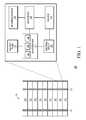
- FIG. 1is a block diagram of a stacked die IC having a die address bus with a programmable width in accordance with at least one embodiment of the present disclosure.
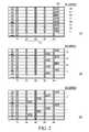
- FIG. 2is a block diagram illustrating different configurations of a data bus of the stacked die IC of FIG. 1 in accordance with at least one embodiment of the present disclosure.
- FIG. 3is a diagram illustrating an arrangement of through-silicon vias (TSVs) at a die of the stacked die IC of FIG. 1 in accordance with at least one embodiment of the present disclosure.
- TSVsthrough-silicon vias
- FIG. 4is a diagram illustrating a technique to stack dies of the stacked die IC of FIG. 1 in order to align TSVs of the dies in accordance with at least one embodiment of the present disclosure.
- FIG. 5is a diagram illustrating another technique to stack dies of the stacked die IC of FIG. 1 in order to align TSVs of the dies in accordance with at least one embodiment of the present disclosure.
- FIG. 6is a block diagram of a system for stacking dies in a stacked die IC and programming a die address bus width of the stacked die IC in accordance with at least one embodiment of the present disclosure.
- FIG. 7is a flow diagram of a identifying a die address bus width in accordance with at least one embodiment of the present disclosure.
- FIG. 8is a flow diagram of a method of stacking dies in a stacked die IC and programming a die address bus width of the stacked die IC in accordance with at least one embodiment of the present disclosure.
- FIGS. 1-8illustrate techniques for providing a stacked die IC having a die address bus having a programmable width.
- the dies of the stacked die ICemploy the address bus to indicate the particular die, or set of dies, targeted by data on a data bus.
- the ICis programmed with information indicating a width of the address bus.
- each die in the die stackhas a common address bus width. This allows the die stack to be configured in different ways for different devices or intended uses, without the need to redesign each die.
- the dies in the stacked die ICare memory devices stacked on top of a die incorporating a memory controller.
- each of the memory diesbe individually addressable, and data exchanged between the dies and the memory controller via an N-bit wide data bus.
- the memory diesbe configured in sets of pairs, thereby allowing each set to exchange data with the memory controller using a 2N-bit wide bus. Because of the different configuration of the die stacks, the die address bus for each configuration is different. Conventionally, in order to accommodate the different bus widths, different dies would be designed and manufactured for each of the different configurations. Using the techniques described herein, the same dies could be used in either configuration, thereby reducing production costs.
- each die in the stacked die ICis formed to include TSVs that, when the dies are stacked together, form a data bus that traverses the die stack.
- Different subsets of the TSVsform respective subsets of the data bus.
- the data buscan be 32 bits wide grouped into four subsets of eight bits each.
- Each dieincludes thirty-two TSVs for the data bus, grouped into four subsets of eight TSVs each, corresponding to the 4 subsets of the data bus.
- Each dieis formed so that the subsets of TSVs are arranged symmetrically about two centerlines of a top face of the die. The same corresponding subset of data bus TSVs are connected to a corresponding functional module of each die.
- each TSV subsetincludes N TSVs
- an N-bit wide data buscan be formed by stacking each die with the top face pointing in the same direction.
- a 2N-bit wide data buscan be formed by grouping the dies into pairs, and flipping one die of each pair so that the top faces of each pair of dies face each other.
- a 4N-bit wide data buscan also be formed, as described further herein.
- the symmetrical arrangement of the TSVs, together with the die address bus having a programmable widthallows for the dies to be used in a wide variety of configurations, improving die flexibility and reducing production costs.
- FIG. 1illustrates a block diagram of a stacked die IC 100 in accordance with one embodiment of the present disclosure.
- the stacked die IC 100is an integrated circuit device including a die stack 101 having dies 102 - 110 .
- the die stack 101is formed with die 110 at the bottom, die 109 stacked on die 110 , die 108 stacked on die 109 , die 107 stacked on die 108 , and so on, with die 102 stacked on die 103 and forming the top of the stack 101 .
- Each of the dies 102 - 110is a semiconductor die including transistors and other components connected so that they form one or more circuits that perform functions for the stacked die IC 100 .
- each of the dies 102 - 108is formed at a different semiconductor wafer.
- the wafersare then aligned, bonded, and singulated into individual stacks, including the stack 101 .
- the dies 102 - 110can be formed at the same wafer, or at different wafers, singulated, and then stacked.
- the modules of the die 110form a general purpose processor, including an instruction pipeline for execution of instructions, cache memory for storage of information for the instruction pipeline, and other processor modules.
- the modules of the dies 102 - 109are memory modules to provide system memory for the processor at the die 110 . Accordingly, the dies 102 - 109 can include storage arrays, address decode modules, and the like, to provide memory storage functionality for the stacked die IC 100 . In some embodiments more or less memory may be stacked on die 110 .
- the dies 102 - 110can be connected via one or more interconnections (e.g., through silicon vias, or TSVs).
- the dies 102 - 110are connected via a die address bus 111 and a data bus 112 each bus comprising multiple TSVs.
- the busses 111 and 112carry information that allows the die 110 to communicate messages, such as memory access requests, to one or more of the dies 102 - 109 .
- each of the dies 102 - 110 , or each subset of the diesis assigned a corresponding die address. The assignment can occur during manufacture of the die stack or by some other method.
- the die 110To communicate a message to a die, or subset of dies, the die 110 places the corresponding address on the die address bus 111 and the content of the message (e.g., memory address information, write data, and the like) on the data bus 112 . As described further herein, the die or subset of dies corresponding to the indicated address receive and process the message content, or a portion thereof. In some cases, in response to a message (e.g., a read access request), the die or subset of dies may return data to the die 110 via the data bus 112 . It will be appreciated that, in some embodiments, each die or subset of dies can communicate messages, and responsive messages or data, to any other of the dies or subset of dies of the die stack 101 . For purposes of description, it will be assumed that die 110 generates messages for provision to the dies 102 - 109 .
- the die 110generates messages for provision to the dies 102 - 109 .
- die address bus 111has a programmable active width (in the following referred to simply as width) which determines whether all or only a subset of the address TSVs will be used to communicate addresses to die in the die stack.
- the die address bus 111includes a number of signal paths, or lines, with each signal line corresponding to a bit of information to be communicated in parallel via the bus.
- the width of the die address bus 111indicates the number of signal lines of the bus that convey information.
- the die address busincludes N signal lines, so that it has a maximum width of N bits.
- a designerdetermines a specified width of the die address bus 111 .
- a wafer probe or other devicestores the specified width at one or more of the dies 102 - 110 .
- each of the dies 102 - 110can include a set of fuses or other non-volatile medium that are programmed by the wafer probe to store the specified width.
- the programming of dies 102 - 110ensures that the addresses placed on the die address bus 111 by die 110 and received by die 102 - 109 match the specified width.
- the specified widthis less than N, the dies 102 - 110 ensure that only the specified number of signal lines are provided with useful information or are read by each die.
- each of the dies 102 - 110adjusts the width of the die address bus 111 , based on the specified width, by coupling one or more of the signal lines to a specified voltage reference (e.g., ground) so that the signal lines cannot communicate useful information.
- each of the dies 102 - 110adjusts the width of the die address bus to the specified width by masking data received via the die address bus 111 , so that the bus effectively conveys addresses only of the specified width.
- the die address bus 111comprises a fixed portion for addressing data within a memory die 102 - 109 and a programmable portion for addressing one or more die 102 - 109 .
- the width of the portion for addressing data within a memoryis fixed by design.
- the programmability of the width of the die address bus 111allows the die stack 101 to be configured in various arrangements without redesign or extensive adjustment of each die.
- the die stack 101can include 8 memory dies (e.g., dies 102 - 109 ) stacked on a processor or memory controller (e.g., die 110 ), similar to the configuration illustrated in FIG. 1 .
- each of the 8 memory diesis assigned a corresponding 3-bit die address, and the assigned address and the width of die selection portion of die address bus 111 is programmed to have a width of 3-bits.
- the die stack 101can include only 4 memory dies stacked on the processor or memory controller, thereby reducing the overall cost and size of the stack.
- each of the 4 memory diesis assigned a corresponding 2 bit address, and the die address bus 111 is programmed to have a width of 2-bits. Because of the programmability of the width of the die address bus 111 , the same memory dies can be used in the 8-die configuration and the 4-die configuration, reducing production costs.
- the dies 102 - 109can be grouped into subsets, with each subset of dies assigned and each die of the subset programmed with a corresponding die address.
- the data bus 112By forming the data bus 112 of sufficient size, this grouping, and the programmability of the width of the die address portion of bus 111 , allows the die stack to be placed in a variety of different configurations without requiring a redesign of the individual dies or changing the number of dies in the stack 101 .
- the die 109includes bus width fuses 131 , a die address register 132 , a die interface 133 , and a functional module 135 .
- the functional module 135is one or more circuits arranged to perform one or more specified functions, such as data storage, input/output signal control and conditioning, instruction execution, and the like.
- the bus width fuses 131are a set of fuses that are programmed, during production of the die 109 , with a value indicating the width of the die address bus 111 .
- the die address register 132is a storage structure that is programmed, during production of the die 109 or some other initialization procedure, with the die address of the die 109 .
- the die interface 133is one or more modules that provide an interface between the functional module 135 , the buses 111 , 112 , and the die address register 132 .
- the die address portion of die address bus 111includes three signal lines, designated signal lines 141 , 142 , and 143 .
- a module of the die 110places the address of the targeted die on the signal lines 141 - 143 of the die address bus 111 .
- the module of the die 110places the message on the data bus 112 .
- the die interface 133determines, based on the bus width fuses 131 , which of the signal lines 141 - 143 carry the die address provided by the die 110 .
- the bus width fuses 131store a binary value of 10 b , indicating that the die address is 2 bits wide.
- the die interface 133determines that the bus address is represented by signals on signal lines 142 and 143 , and that data on signal line 141 can be ignored.
- the die interface 133can therefore identify the bus address by masking data on signal line 141 , by connecting the signal line 141 to a fixed voltage reference that matches a corresponding bit of the die address register, and the like.
- the die interface 133compares the received die address, of the identified address width, to the value programmed into the die address register 132 . In response to identifying a mismatch, the die interface 133 uncouples the data bus 112 from the functional module 135 , so that the message on the data bus 112 is not provided to the functional module 135 . In response to determining that the die address one the die address bus matches the value stored at the die address register 132 , the die interface 133 couples the data bus 112 to the functional module 135 , thereby providing the message from the die 109 to the functional module 135 .
- the internal busses of the functional modules of the dies 102 - 109are of a size M.
- Me.g. 4M
- the die stack 101can be configured in a variety of different ways for different devices. This can be better understood with reference to FIG. 2 , which illustrates configurations 215 , 216 , and 217 of die stack 101 in accordance with at least one embodiment.
- the data bus 112includes four sub-busses, designated sub-busses 251 , 252 , 253 , and 254 . Each sub-bus is an equivalently sized portion of data bus 112 .
- the data bus 112is 32 bits wide, and each of the sub-busses is 8 bits wide.
- the data bus 112 and each of the sub-busses 251 - 254can be of different sizes than in the described example.
- the different configurations 215 - 217use different ones of the sub-busses 251 - 254 to deliver data to their respective functional modules.
- a connection to a functional module of a dieis illustrated by a vertical line with a circle on its right end.
- connection 258 of configuration 215indicates that the functional module of die 102 is connected to sub-bus 254 .
- configuration 215all of the functional modules of the dies 102 - 109 are connected to the sub-bus 254 .
- the data bus 112is effectively an 8-bit wide bus that uses only sub-bus 254 .
- each of the dies 102 - 109is individually addressable with a different 3 bit die address.
- the die address bus 111is programmed to have a width of 3 bits.
- the dies 102 - 109are grouped in pairs.
- the functional module of one of the dies of each pairis connected to sub-bus 254 while the functional module of the other die of each pair is connected to sub-bus 253 .
- dies 102 and 103are grouped into one pair, wherein the functional module of die 102 is connected to sub-bus 254 and the functional module of die 103 is connected to sub-bus 253 .
- the data bus 112is effectively a 16-bit wide bus that uses only sub-busses 253 and 254 .
- each grouped pair of the dies 102 - 109is individually addressable with a different two-bit die address. Accordingly, in configuration 215 the die address bus 111 is programmed to have a width of two bits.
- the dies 102 - 109are grouped in sets of four, wherein the functional module of each die in each set is connected to a respective different one of the sub-busses 251 - 254 .
- dies 102 - 105are grouped into one set, wherein the functional module of die 102 is connected to sub-bus 254 , the functional module of die 103 is connected to sub-bus 253 , the functional module of die 104 is connected to sub-bus 252 , and the functional module of die 105 is connected to sub-bus 251 .
- the data bus 112is effectively a 32-bit wide bus that uses all of the sub-buses 251 - 254 .
- each grouped set of the dies 102 - 109is individually addressable with a different 1 bit die address. Accordingly, in configuration 215 the die address bus 111 is programmed to have a width of one bit.
- the different configurations 215 - 217can be used for different configurations of the die 110 .
- the die 110includes a memory controller, and the functional modules of the dies 102 - 109 are memory modules that can be accessed (read and written) by memory access requests issued by the memory controller.
- the memory controlleremploys an 8 bit wide internal bus, so that it accesses portions of the memory modules 8 bits at a time.
- the die stack 101can be arranged in configuration 215 .
- the memory controlleremploys a 16 bit wide internal data bus, so that it accesses portions of the memory modules 16 bits at a time.
- the die stack 101can be arranged in configuration 216 .
- each memory accessis partially satisfied by each die in the addressed pair. For example, for a write access to a memory location, one die in the addressed pair stores half of the write data and the other die in the addressed pair stores the other half. For a read access to the memory location, one die in the addressed pair provides half of the read data and the other die in the addressed pair provides the other half.
- the memory controlleremploys a 32 bit wide internal data bus, so that it accesses portions of the memory modules 32 bits at a time.
- the die stack 101can be arranged in configuration 217 .
- each memory accessis partially satisfied by each die in the addressed group, in similar fashion to that described above with respect to configuration 215 , but with each die in the group storing or providing one-fourth of the write or read data.
- the die stack 101can be configured in various arrangements without requiring a specialized die for each configuration, reducing design and production costs.
- each of the functional modules of each of the dies 102 - 109is connected to all of the sub-busses 251 - 254 via corresponding fuses.
- the fuses of the diesare programmed such that the functional modules of each die are connected to the appropriate sub-bus.
- an interface for each bit of the data busmust be provided and along with switches to direct data to the appropriate bit of the data bus depending on the programmed die address bus width and the programmed die address. Unused interfaces to the data bus are tri-stated.
- each of the dies 102 - 109is formed with sets of TSVs to cumulatively support the width of the widest data bus programmable option. Only one of the subset or port of a subset of TSVs is connected by design to the functional module of the die address programmable die, and the configurations 215 - 217 can be formed by appropriately orienting each die in the die stack 101 . This can be better understood with reference to FIGS. 3-5 .
- FIG. 3illustrates a top-view diagram of the die 109 in accordance with at least embodiment of the present disclosure.
- the die 109includes a top face 330 opposite a bottom face (not shown). It will be appreciated that the terms “top face” and “bottom face” refer to relative positions of faces of the die 109 , and do not necessarily refer to any particular orientation of the faces in space.
- the die 109also includes TSV sets 335 , 336 , 337 , and 338 , each including 8 TSVs. When the die 109 is stacked in the die stack 101 , each of the TSV sets 335 - 338 forms a portion of a corresponding one of the sub-busses 251 - 254 . Further, only the TSVs of set 335 are connected to the functional module of the die 109 .
- the sets 336 , 338 , 337 of TSVsare electrically isolated from die 109 .
- the top face of the die 109is symmetrical about two orthogonal centerlines, designated centerline 340 and centerline 341 , respectively.
- Centerline 340runs through the center of the top face 330 parallel to the perimeter of the top face 330 in one direction (the “horizontal” direction in the depicted example).
- Centerline 341is orthogonal to centerline 340 , and runs through the center of the top face 330 parallel to the perimeter of the top face 330 in a direction orthogonal (the “vertical” direction in the depicted example) to that of the centerline 340 .
- the sets 335 - 338 of TSVsare arranged symmetrically about the centerlines 340 and 341 .
- TSV set 335is above centerline 340 and to the left of centerline 341
- TSV set 336is above centerline 340 and to the right of centerline 341
- TSV set 337is below centerline 340 and to the left of centerline 341
- TSV set 335is below centerline 340 and to the right of centerline 341 .
- the die 109is formed so that each of the TSV sets 335 - 338 is the same respective distance from each of the centerlines 340 and 341 .
- TSV set 335forms a portion of sub-bus 254
- TSV set 336forms a portion of sub-bus 252
- TSV set 337forms a portion of sub-bus 253
- TSV set 338forms a portion of sub-bus 251 .
- the die 109is rotated about the centerline 340 , such that the top face 330 faces towards a bottom of the die stack 101 .
- the TSV set 335is in the “bottom, left” portion of the face 330 when viewed from the top (i.e., in the position formerly occupied by TSV set 337 prior to rotation).
- TSV set 335forms a portion of sub-bus 253
- TSV set 336forms a portion of sub-bus 251
- TSV set 337forms a portion of sub-bus 254
- TSV set 338forms a portion of sub-bus 252 .
- die 109also includes additional TSVs, such as TSVs 375 and 376 that provide signal lines (or portions thereof) for control signals such as, clock signals, write enable signals, and the like.
- TSVs 376are placed on the centerline 340 with corresponding TSVs 376 mirrored about centerline 341 .
- TSVs 376are each internally coupled to a corresponding TSV of TSVs 376 so that a die with any die orientation relative to die 109 will have a set of control signal TSVs coupled to the appropriate TSV of TSVs 375 of die 109 , thus forming a signal path for the associated control signal through the die stack 101 .
- the TSVs 375 and 376can form signal paths for signals other than control signals.
- any of the configurations 215 - 217 of FIG. 2can be created.
- configuration 215can be created by placing each of the dies 102 - 109 in a similar position of die 109 of FIG. 3 , such that their respective top faces all face towards a top of the die stack 101 . In this configuration, all of the functional modules of the dies 102 - 109 are connected to the same sub-bus of data bus 112 , as in configuration 215 .
- FIG. 4illustrates an arrangement of a pair of dies in a configuration corresponding to configuration 216 of FIG. 2 in accordance with at least one embodiment of the present disclosure.
- the illustrated exampleillustrates identical dies 102 and 103 from a top position, similar to the view of die 109 of FIG. 3 .
- the dies 102 and 103are each formed similarly to the die 109 of FIG. 3 to each have four TSV sets arranged symmetrically about their respective centerlines.
- Die 102includes a TSV set 441 , indicated by black circles, which is connected to the functional module of die 102 .
- die 103includes a TSV set 442 , indicated by black diamonds, which is connected to the functional module of die 103 .
- the die 103is flipped about its centerline so that its top face faces in an opposite direction to the top face of die 102 .
- thisplaces the TSV set 442 below the TSV set 441 , so that, when stacked in the die stack 101 , the TSV sets 441 forms a portion of the sub-bus 254 while TSV set 442 forms a portion of the sub-bus 253 .
- each dieis connected to different ones of the sub-busses 253 and 254 , as illustrated by configuration 216 of FIG. 2 .
- Other pairs of dies, as illustrated by configuration 216can be similarly arranged.
- different configurationscan be created by differently positioning different dies, obviating the need to program the sub-bus connections for each die or have a specially designed die for each possible sub-bus connection.
- FIG. 5illustrates an arrangement of a set of four dies in a configuration corresponding to configuration 217 of FIG. 2 in accordance with at least one embodiment of the present disclosure.
- the illustrated exampleillustrates dies 102 , 103 , 104 , and 105 from a top position, similar to the view of die 109 of FIG. 3 .
- the dies 102 - 105are each formed similarly to the die 109 of FIG. 3 to each have four TSV sets arranged symmetrically about their respective centerlines.
- Die 102includes a TSV set 541 , indicated by black circles, which is connected to the functional module of die 102 .
- die 103includes a TSV set 542 , indicated by black diamonds, which is connected to the functional module of die 103 .
- Die 104includes a TSV set 543 , indicated by black squares, which is connected to the functional module of die 104
- die 105includes a TSV set 544 , indicated by black triangles, which is connected to the functional module of die 105 .
- the dies 102 - 105are identical, including programming of the die address bus width at each die.
- the die 103is flipped about its horizontal centerline so that its top face faces in an opposite direction to the top face of die 102 .
- Dies 104is rotated 180 degrees to position the TSV set 543 as illustrated at FIG. 4 .
- Die 105is rotated 180 degrees and then flipped to position the TSV set 544 as illustrated at FIG. 4 .
- the TSV set 542is below the TSV set 541
- TSV set 543is to the right of TSV set 541
- TSV set 544is below TSV set 543 and to the right of TSV set 542 .
- the TSV sets 541forms a portion of the sub-bus 254
- TSV set 542forms a portion of the sub-bus 253
- TSV set 543forms a portion of the sub-bus 252
- TSV set 544forms a portion of the sub-bus 251 .
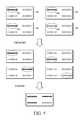
- FIG. 6is a block diagram of a die stacking system 600 in accordance with at least one embodiment of the present disclosure.
- the system 600includes a die programming control module 666 connected to a probe 663 .
- the die programming control module 666is a computer device, and associated manufacturing equipment, generally configured to select one or more dies from a set 660 of dies based on a design specification, computer readable control file, or other design information (not shown).
- the die programming controlhas selected a die 601 .
- the die 601is part of a semiconductor wafer including multiple dies.
- the die 601is an individual die that has previously been singulated from a semiconductor wafer.
- the probe 663is manufacturing equipment configured to apply electrical signaling to terminals of the die 601 in order to program fuses or otherwise store configuration data at storage modules of the die 601 .
- the die programming control module 666accesses design information to identify the values that are to be programmed at one or more storage modules (e.g., one or more fuses) of the die 601 .
- the die programming control module 666controls the probe 663 to apply the electrical signaling to program the identified values at the corresponding storage modules of the die 601 .
- the die programming control module 666identifies, based on the design information, the width of the die address bus for the die 601 , and controls the probe 663 to program a value indicating the bus width at die address register of the die 601 .
- the die programming control module 666can also program the die 601 with information indicating the die address assigned to the die 601 .
- the system 600includes a die positioner 667 and a die stacker 668 .
- the die positioner 667includes a computer device and associated equipment to rotate the die 601 , resulting in a positioned die 602 .
- the die positioner 667rotates the die 601 to align a set of TSVs connected to a corresponding functional module with the TSV sets of one or more other dies (not shown) so that the functional module of the die 601 is connected to a sub-bus of a data bus, in similar fashion to that described above with respect to FIGS. 2-5 .
- the die stacker 668stacks the positioned die, together with other positioned die, into a stacked die 605 .
- the die stacker 668can include equipment to ensure that the dies to be stacked are aligned, equipment to place each die on the stack in its specified position, and equipment to bond the die to each other.
- the system 600performs its operations on semiconductor wafers including multiple dies.
- the system 600programs the die address bus width and the same die address value at each die on the wafer, then positions the wafer such that each die of the wafer has the same orientation.
- the system 600stacks the wafer with other programmed and positioned wafers, resulting in multiple stacked die arrangements.
- the system 600can then singulate the stacked dies from the wafers.
- the system 600performs its operations on a single semiconductor wafer.
- the system 600programs the die address bus width and a different die address value at each die on the wafer.
- the system 600then singulates the dies on the wafer, positions the singulated dies as described with respect to FIGS. 2-5 according to a specified configuration, and stacks the positioned dies.
- FIG. 7illustrates a method 700 of identifying a bus address at a die of a stacked die IC in accordance with at least one embodiment of the present disclosure.
- the diereceives an address at a die address bus of the stacked die IC, the address corresponding to a message on a data bus of the stacked die IC.
- the diedetermines, based on a set of programmed fuses, a width of the die address bus.
- the dieidentifies, based on the width of the die address bus, which signal lines of the die address bus the die address is to be read from.
- the diereads the die address from the identified signal lines.
- the diecompares the read die address to a stored die address value to determine if the message is targeted to the die.
- FIG. 8illustrates a flow diagram of a method 800 of forming a stacked die having a die address bus with a programmable width, in accordance with at least one embodiment of the present disclosure.
- a dieis formed to have a storage module (e.g., a set of fuses) to store a value indicating a width of a die bus address.
- the dieis also formed to have a set of TSVs to form a part of the die address bus and sets of TSVs to form different portions, or sub-busses, of a data bus.
- the dieis formed so that different sets of TSVs for the different portions of the data bus are arranged in symmetrical positions about one or more centerlines of a top surface of the die, in similar fashion to that illustrated above in FIG. 3 .
- the dieis formed so that a functional module of the die is connected to only one of the different sets of TSVs that form different portions of the data bus.
- a die programming control moduledetermines, based on a design file or other specification, a specified width of the die address bus for the die stack that is to include the die formed at block 802 .
- the die programming control moduleprograms the storage module of the die with a value indicating the specified width.
- the die programming control moduledetermines, based on the design file or other specification, the die address to be assigned to the die, and programs a storage module of the die with the specified address.
- a die positioneridentifies, based on the design file or other specification, which portion of a data bus of the stacked die is to be connected to the functional module of the die formed at block 802 .
- the die positionerdetermines, for the identified portion of the data bus, the position of the die so that the set of TSVs connected to the functional module are aligned with TSVs of other dies to form the identified portion.
- the identified portionrequires the die to be flipped about a centerline or rotated, as described above in the examples of FIGS. 4 and 5 .
- the die positionerplaces the die in the position identified at block 808 , including by performing any necessary rotations of the die.
- a die stackerstacks the positioned die on the die stack.
- certain aspects of the techniques described abovemay implemented by one or more processors of a processing system executing software.
- the softwarecomprises one or more sets of executable instructions stored or otherwise tangibly embodied on a non-transitory computer readable storage medium.
- the softwarecan include the instructions and certain data that, when executed by the one or more processors, manipulate the one or more processors to perform one or more aspects of the techniques described above.
- the non-transitory computer readable storage mediumcan include, for example, a magnetic or optical disk storage device, solid state storage devices such as Flash memory, a cache, random access memory (RAM) or other non-volatile memory device or devices, and the like.
- the executable instructions stored on the non-transitory computer readable storage mediummay be in source code, assembly language code, object code, or other instruction format that is interpreted or otherwise executable by one or more processors.
- a computer readable storage mediummay include any storage medium, or combination of storage media, accessible by a computer system during use to provide instructions and/or data to the computer system.
- Such storage mediacan include, but is not limited to, optical media (e.g., compact disc (CD), digital versatile disc (DVD), Blu-Ray disc), magnetic media (e.g., floppy disc, magnetic tape, or magnetic hard drive), volatile memory (e.g., random access memory (RAM) or cache), non-volatile memory (e.g., read-only memory (ROM) or Flash memory), or microelectromechanical systems (MEMS)-based storage media.
- optical mediae.g., compact disc (CD), digital versatile disc (DVD), Blu-Ray disc
- magnetic mediae.g., floppy disc, magnetic tape, or magnetic hard drive
- volatile memorye.g., random access memory (RAM) or cache
- non-volatile memorye.g., read-only memory (ROM) or Flash memory
- MEMSmicroelectro
- the computer readable storage mediummay be embedded in the computing system (e.g., system RAM or ROM), fixedly attached to the computing system (e.g., a magnetic hard drive), removably attached to the computing system (e.g., an optical disc or Universal Serial Bus (USB)-based Flash memory), or coupled to the computer system via a wired or wireless network (e.g., network accessible storage (NAS)).
- system RAM or ROMsystem RAM or ROM
- USBUniversal Serial Bus
- NASnetwork accessible storage
Landscapes
- Engineering & Computer Science (AREA)
- Microelectronics & Electronic Packaging (AREA)
- Power Engineering (AREA)
- Physics & Mathematics (AREA)
- General Physics & Mathematics (AREA)
- Condensed Matter Physics & Semiconductors (AREA)
- Computer Hardware Design (AREA)
- Theoretical Computer Science (AREA)
- Manufacturing & Machinery (AREA)
- General Engineering & Computer Science (AREA)
- Semiconductor Integrated Circuits (AREA)
Abstract
Description
Claims (11)
Priority Applications (1)
| Application Number | Priority Date | Filing Date | Title |
|---|---|---|---|
| US14/525,347US10002653B2 (en) | 2014-10-28 | 2014-10-28 | Die stack address bus having a programmable width |
Applications Claiming Priority (1)
| Application Number | Priority Date | Filing Date | Title |
|---|---|---|---|
| US14/525,347US10002653B2 (en) | 2014-10-28 | 2014-10-28 | Die stack address bus having a programmable width |
Publications (2)
| Publication Number | Publication Date |
|---|---|
| US20160118095A1 US20160118095A1 (en) | 2016-04-28 |
| US10002653B2true US10002653B2 (en) | 2018-06-19 |
Family
ID=55792491
Family Applications (1)
| Application Number | Title | Priority Date | Filing Date |
|---|---|---|---|
| US14/525,347Active2035-03-20US10002653B2 (en) | 2014-10-28 | 2014-10-28 | Die stack address bus having a programmable width |
Country Status (1)
| Country | Link |
|---|---|
| US (1) | US10002653B2 (en) |
Families Citing this family (5)
| Publication number | Priority date | Publication date | Assignee | Title |
|---|---|---|---|---|
| US11721653B2 (en) | 2019-12-23 | 2023-08-08 | Adeia Semiconductor Bonding Technologies Inc. | Circuitry for electrical redundancy in bonded structures |
| CN115088068A (en) | 2019-12-23 | 2022-09-20 | 伊文萨思粘合技术公司 | Electrical redundancy for bonded structures |
| US11954040B2 (en)* | 2020-06-15 | 2024-04-09 | Arm Limited | Cache memory architecture |
| US12107076B2 (en)* | 2021-12-28 | 2024-10-01 | Advanced Micro Devices, Inc. | Through-silicon via layout for multi-die integrated circuits |
| US12255178B2 (en)* | 2022-01-26 | 2025-03-18 | Mellanox Technologies, Ltd | Mirror image of geometrical patterns in stacked integrated circuit dies |
Citations (81)
| Publication number | Priority date | Publication date | Assignee | Title |
|---|---|---|---|---|
| US5019943A (en) | 1990-02-14 | 1991-05-28 | Unisys Corporation | High density chip stack having a zigzag-shaped face which accommodates connections between chips |
| US5434745A (en) | 1994-07-26 | 1995-07-18 | White Microelectronics Div. Of Bowmar Instrument Corp. | Stacked silicon die carrier assembly |
| US5675180A (en) | 1994-06-23 | 1997-10-07 | Cubic Memory, Inc. | Vertical interconnect process for silicon segments |
| US5998860A (en) | 1997-12-19 | 1999-12-07 | Texas Instruments Incorporated | Double sided single inline memory module |
| US6259622B1 (en) | 1998-07-07 | 2001-07-10 | Dsp Group, Inc. | Two bit per cell ROM using a two phase current sense amplifier |
| US6281577B1 (en) | 1996-06-28 | 2001-08-28 | Pac Tech-Packaging Technologies Gmbh | Chips arranged in plurality of planes and electrically connected to one another |
| US20010045645A1 (en) | 2000-04-20 | 2001-11-29 | Kabushiki Kaisha Toshiba | Multichip semiconductor device and memory card |
| US6337227B1 (en) | 1996-02-20 | 2002-01-08 | Micron Technology, Inc. | Method of fabrication of stacked semiconductor devices |
| US6427156B1 (en) | 1997-01-21 | 2002-07-30 | Xilinx, Inc. | Configurable logic block with AND gate for efficient multiplication in FPGAS |
| US20020157082A1 (en) | 1997-09-30 | 2002-10-24 | Jeng-Jye Shau | Inter-dice wafer level signal transfer methods for integrated circuits |
| US20020182772A1 (en) | 1998-08-21 | 2002-12-05 | Moden Walter L. | Low profile multi-IC chip package connector |
| US20020190371A1 (en) | 2001-06-14 | 2002-12-19 | Shinko Electric Industries Co., Ltd. | Semiconductor device and method of production of same |
| US20030080408A1 (en) | 1997-12-18 | 2003-05-01 | Farnworth Warren M. | Method for fabricating semiconductor components and interconnects with contacts on opposing sides |
| US20030106212A1 (en) | 2000-04-08 | 2003-06-12 | Advanced Semiconductor Engineering, Inc. | Method of attaching a heat sink to an IC package |
| US20030107119A1 (en) | 2001-12-06 | 2003-06-12 | Samsung Electronics Co., Ltd. | Multi-chip package (MCP) with a conductive bar and method for manufacturing the same |
| US6603072B1 (en) | 2001-04-06 | 2003-08-05 | Amkor Technology, Inc. | Making leadframe semiconductor packages with stacked dies and interconnecting interposer |
| US6664485B2 (en) | 1998-03-25 | 2003-12-16 | International Business Machines Corporation | Full additive process with filled plated through holes |
| US20040009631A1 (en) | 2002-07-10 | 2004-01-15 | Mike Connell | Semiconductor package with circuit side polymer layer and wafer level fabrication method |
| US6716676B2 (en) | 2001-06-04 | 2004-04-06 | Siliconware Precision Industries Co., Ltd. | Thermally-enhanced stacked-die ball grid array semiconductor package and method of fabricating the same |
| US20040069988A1 (en) | 2002-10-11 | 2004-04-15 | Taiwan Semiconductor Manufacturing Co. Ltd. | Bonding pad with separate bonding and probing areas |
| US20050023677A1 (en) | 2002-02-01 | 2005-02-03 | Broadcom Corporation | Method for assembling a ball grid array package with multiple interposers |
| US20050051883A1 (en) | 2003-06-19 | 2005-03-10 | Seiko Epson Corporation | Semiconductor device and method of manufacturing the same, circuit board, and electronic instrument |
| US20050104171A1 (en) | 2003-11-13 | 2005-05-19 | Benson Peter A. | Microelectronic devices having conductive complementary structures and methods of manufacturing microelectronic devices having conductive complementary structures |
| US20050104219A1 (en) | 2003-09-26 | 2005-05-19 | Kuniyasu Matsui | Intermediate chip module, semiconductor device, circuit board, and electronic device |
| US20050104183A1 (en) | 2003-11-17 | 2005-05-19 | Renesas Technology Corp. | Multi-chip module |
| US20050156333A1 (en) | 2003-09-11 | 2005-07-21 | Super Talent Electronics Inc. | Narrow Universal-Serial-Bus (USB) Flash-Memory Card with Straight Sides using a Ball-Grid-Array (BGA) Chip |
| US7061092B2 (en) | 1999-02-01 | 2006-06-13 | Micron Technology, Inc. | High-density modularity for ICS |
| US20060216862A1 (en) | 2003-11-13 | 2006-09-28 | Micron Technology, Inc. | Microelectronic devices, methods for forming vias in microelectronic devices, and methods for packaging microelectronic devices |
| US20060278979A1 (en) | 2005-06-09 | 2006-12-14 | Intel Corporation | Die stacking recessed pad wafer design |
| US7198979B2 (en) | 2002-11-04 | 2007-04-03 | Infineon Technologies Ag | Method for manufacturing a stack arrangement of a memory module |
| US20070145558A1 (en) | 2002-05-21 | 2007-06-28 | Micron Technology, Inc. | Super high density module with integrated wafer level packages |
| US20070181998A1 (en) | 2006-02-03 | 2007-08-09 | Stats Chippac Ltd. | Stacked integrated circuit package system with face to face stack configuration |
| US7271482B2 (en) | 2004-12-30 | 2007-09-18 | Micron Technology, Inc. | Methods for forming interconnects in microelectronic workpieces and microelectronic workpieces formed using such methods |
| US20080001283A1 (en) | 2006-06-29 | 2008-01-03 | Ha Na Lee | Stack package with vertically formed heat sink |
| US7344969B2 (en) | 2002-01-09 | 2008-03-18 | Micron Technology, Inc. | Stacked die in die BGA package |
| US7371677B2 (en) | 2005-09-30 | 2008-05-13 | Freescale Semiconductor, Inc. | Laterally grown nanotubes and method of formation |
| US20080237887A1 (en) | 2007-03-29 | 2008-10-02 | Hem Takiar | Semiconductor die stack having heightened contact for wire bond |
| US20080284045A1 (en) | 2007-05-18 | 2008-11-20 | Texas Instruments Incorporated | Method for Fabricating Array-Molded Package-On-Package |
| US20090001602A1 (en) | 2007-06-26 | 2009-01-01 | Qwan Ho Chung | Stack package that prevents warping and cracking of a wafer and semiconductor chip and method for manufacturing the same |
| US20090001543A1 (en) | 2007-06-26 | 2009-01-01 | Qwan Ho Chung | Lightweight and compact through-silicon via stack package with excellent electrical connections and method for manufacturing the same |
| US20090014843A1 (en) | 2007-06-06 | 2009-01-15 | Kawashita Michihiro | Manufacturing process and structure of through silicon via |
| US20090032966A1 (en) | 2007-08-01 | 2009-02-05 | Jong Ho Lee | Method of fabricating a 3-D device and device made thereby |
| US20090051043A1 (en) | 2007-08-21 | 2009-02-26 | Spansion Llc | Die stacking in multi-die stacks using die support mechanisms |
| US20090085608A1 (en) | 2007-10-02 | 2009-04-02 | Micron Technology, Inc. | Systems, methods and devices for arbitrating die stack position in a multi-bit stack device |
| US7514776B2 (en) | 2001-03-15 | 2009-04-07 | Micron Technology, Inc. | Semiconductor/printed circuit board assembly, and computer system |
| US20090102038A1 (en) | 2007-10-18 | 2009-04-23 | Vertical Circuits, Inc. | Chip scale stacked die package |
| US20090121615A1 (en) | 2007-11-14 | 2009-05-14 | Cree, Inc. | Cerium and Europium Doped Phosphor Compositions and Light Emitting Devices Including the Same |
| US7560304B2 (en) | 2006-12-28 | 2009-07-14 | Sandisk Corporation | Method of making a semiconductor device having multiple die redistribution layer |
| US20090194855A1 (en) | 2008-02-05 | 2009-08-06 | Yong Liu | Folded leadframe multiple die package |
| US20090243064A1 (en) | 2008-03-31 | 2009-10-01 | Stats Chippac, Ltd. | Method and Apparatus For a Package Having Multiple Stacked Die |
| US20090302435A1 (en) | 2008-06-04 | 2009-12-10 | Stats Chippac, Ltd. | Semiconductor Device and Method of Shielding Semiconductor Die from Inter-Device Interference |
| US20100007001A1 (en) | 2008-07-11 | 2010-01-14 | David Wei Wang | Semiconductor package structure and method for manufacturing the same |
| US20100062621A1 (en) | 2008-09-11 | 2010-03-11 | Michael Bruennert | Horizontal Dual In-line Memory Modules |
| US20100109134A1 (en) | 2008-10-31 | 2010-05-06 | Jereza Armand Vincent C | Pre-molded, clip-bonded multi-die semiconductor package |
| US20100109137A1 (en) | 2008-11-03 | 2010-05-06 | Headway Technologies, Inc. | Layered chip package with heat sink |
| US20100123234A1 (en) | 2008-11-14 | 2010-05-20 | Chipmos Technologies Inc. | Multi-chip package and manufacturing method thereof |
| US20100133645A1 (en) | 2008-11-26 | 2010-06-03 | Stmicroelectronics (Rousset) Sas | Method for stacking and interconnecting integrated circuits |
| US7777330B2 (en) | 2008-02-05 | 2010-08-17 | Freescale Semiconductor, Inc. | High bandwidth cache-to-processing unit communication in a multiple processor/cache system |
| US20100213603A1 (en) | 2009-02-20 | 2010-08-26 | National Semiconductor Corporation | Integrated circuit micro-module |
| US20110001240A1 (en) | 2006-08-15 | 2011-01-06 | Stats Chippac, Ltd. | Chip Scale Module Package in BGA Semiconductor Package |
| US20110024888A1 (en) | 2009-07-31 | 2011-02-03 | Stats Chippac, Ltd. | Semiconductor Device and Method of Mounting Die with TSV in Cavity of Substrate for Electrical Interconnect of FI-POP |
| US20110057306A1 (en) | 2009-09-04 | 2011-03-10 | Mcshane Michael B | Edge mounted integrated circuits with heat sink |
| US7928590B2 (en) | 2006-08-15 | 2011-04-19 | Qimonda Ag | Integrated circuit package with a heat dissipation device |
| US20110090004A1 (en) | 2009-10-19 | 2011-04-21 | Mosaid Technologies Incorporated | Reconfiguring through silicon vias in stacked multi-die packages |
| US7939920B2 (en) | 2005-11-01 | 2011-05-10 | Sandisk Corporation | Multiple die integrated circuit package |
| US20110109381A1 (en)* | 2009-11-11 | 2011-05-12 | International Business Machines Corporation | Integrated Circuit Die Stacks With Rotationally Symmetric Vias |
| US20110156233A1 (en) | 2009-12-31 | 2011-06-30 | Hynix Semiconductor Inc. | Stack package |
| US20110175215A1 (en) | 2010-01-19 | 2011-07-21 | International Business Machines Corporation | 3d chip stack having encapsulated chip-in-chip |
| US20110215355A1 (en) | 2010-03-08 | 2011-09-08 | Van De Ven Antony P | Photonic crystal phosphor light conversion structures for light emitting devices |
| US20110316158A1 (en) | 2010-06-29 | 2011-12-29 | Lai Nguk Chin | Method and system for thin multi chip stack package with film on wire and copper wire |
| US20120038057A1 (en) | 2010-08-13 | 2012-02-16 | International Business Machines Corporation | Thermal enhancement for multi-layer semiconductor stacks |
| US20120113617A1 (en) | 2010-11-10 | 2012-05-10 | Osram Sylvania Inc. | Luminescent Ceramic Converter and LED Containing Same |
| US20120134193A1 (en)* | 2010-11-30 | 2012-05-31 | Elpida Memory, Inc. | Semiconductor device having plural memory chip |
| US20120201068A1 (en) | 2009-10-23 | 2012-08-09 | Ware Frederick A | Stacked semiconductor device |
| US20130091315A1 (en) | 2011-10-11 | 2013-04-11 | Etron Technology, Inc. | High speed memory chip module and electronics system device with a high speed memory chip module |
| US20130088255A1 (en) | 2011-10-07 | 2013-04-11 | Perry H. Pelley | Stacked semiconductor devices |
| US20130105991A1 (en) | 2011-11-02 | 2013-05-02 | Stmicroelectronics Pte Ltd. | Embedded wafer level package for 3d and package-on-package applications, and method of manufacture |
| US8436460B1 (en) | 2007-05-04 | 2013-05-07 | Cypress Semiconductor Corporation | Multiple die paddle leadframe and semiconductor device package |
| US8472232B2 (en) | 2005-08-30 | 2013-06-25 | Micron Technology, Inc. | Self-identifying stacked die semiconductor components |
| US20140084444A1 (en) | 2012-09-21 | 2014-03-27 | Taiwan Semiconductor Manufacturing Company, Ltd. | Thermal Dissipation Through Seal Rings in 3DIC Structure |
| US20140264383A1 (en) | 2013-03-15 | 2014-09-18 | Renesas Electronics Corporation | Semiconductor device and manufacturing method of the same |
- 2014
- 2014-10-28USUS14/525,347patent/US10002653B2/enactiveActive
Patent Citations (82)
| Publication number | Priority date | Publication date | Assignee | Title |
|---|---|---|---|---|
| US5019943A (en) | 1990-02-14 | 1991-05-28 | Unisys Corporation | High density chip stack having a zigzag-shaped face which accommodates connections between chips |
| US5675180A (en) | 1994-06-23 | 1997-10-07 | Cubic Memory, Inc. | Vertical interconnect process for silicon segments |
| US5434745A (en) | 1994-07-26 | 1995-07-18 | White Microelectronics Div. Of Bowmar Instrument Corp. | Stacked silicon die carrier assembly |
| US6337227B1 (en) | 1996-02-20 | 2002-01-08 | Micron Technology, Inc. | Method of fabrication of stacked semiconductor devices |
| US6281577B1 (en) | 1996-06-28 | 2001-08-28 | Pac Tech-Packaging Technologies Gmbh | Chips arranged in plurality of planes and electrically connected to one another |
| US6427156B1 (en) | 1997-01-21 | 2002-07-30 | Xilinx, Inc. | Configurable logic block with AND gate for efficient multiplication in FPGAS |
| US20020157082A1 (en) | 1997-09-30 | 2002-10-24 | Jeng-Jye Shau | Inter-dice wafer level signal transfer methods for integrated circuits |
| US20030080408A1 (en) | 1997-12-18 | 2003-05-01 | Farnworth Warren M. | Method for fabricating semiconductor components and interconnects with contacts on opposing sides |
| US5998860A (en) | 1997-12-19 | 1999-12-07 | Texas Instruments Incorporated | Double sided single inline memory module |
| US6664485B2 (en) | 1998-03-25 | 2003-12-16 | International Business Machines Corporation | Full additive process with filled plated through holes |
| US6259622B1 (en) | 1998-07-07 | 2001-07-10 | Dsp Group, Inc. | Two bit per cell ROM using a two phase current sense amplifier |
| US20020182772A1 (en) | 1998-08-21 | 2002-12-05 | Moden Walter L. | Low profile multi-IC chip package connector |
| US7061092B2 (en) | 1999-02-01 | 2006-06-13 | Micron Technology, Inc. | High-density modularity for ICS |
| US20030106212A1 (en) | 2000-04-08 | 2003-06-12 | Advanced Semiconductor Engineering, Inc. | Method of attaching a heat sink to an IC package |
| US20010045645A1 (en) | 2000-04-20 | 2001-11-29 | Kabushiki Kaisha Toshiba | Multichip semiconductor device and memory card |
| US7514776B2 (en) | 2001-03-15 | 2009-04-07 | Micron Technology, Inc. | Semiconductor/printed circuit board assembly, and computer system |
| US6603072B1 (en) | 2001-04-06 | 2003-08-05 | Amkor Technology, Inc. | Making leadframe semiconductor packages with stacked dies and interconnecting interposer |
| US6716676B2 (en) | 2001-06-04 | 2004-04-06 | Siliconware Precision Industries Co., Ltd. | Thermally-enhanced stacked-die ball grid array semiconductor package and method of fabricating the same |
| US20020190371A1 (en) | 2001-06-14 | 2002-12-19 | Shinko Electric Industries Co., Ltd. | Semiconductor device and method of production of same |
| US20030107119A1 (en) | 2001-12-06 | 2003-06-12 | Samsung Electronics Co., Ltd. | Multi-chip package (MCP) with a conductive bar and method for manufacturing the same |
| US7344969B2 (en) | 2002-01-09 | 2008-03-18 | Micron Technology, Inc. | Stacked die in die BGA package |
| US20050023677A1 (en) | 2002-02-01 | 2005-02-03 | Broadcom Corporation | Method for assembling a ball grid array package with multiple interposers |
| US20070145558A1 (en) | 2002-05-21 | 2007-06-28 | Micron Technology, Inc. | Super high density module with integrated wafer level packages |
| US20040009631A1 (en) | 2002-07-10 | 2004-01-15 | Mike Connell | Semiconductor package with circuit side polymer layer and wafer level fabrication method |
| US20040069988A1 (en) | 2002-10-11 | 2004-04-15 | Taiwan Semiconductor Manufacturing Co. Ltd. | Bonding pad with separate bonding and probing areas |
| US7198979B2 (en) | 2002-11-04 | 2007-04-03 | Infineon Technologies Ag | Method for manufacturing a stack arrangement of a memory module |
| US20050051883A1 (en) | 2003-06-19 | 2005-03-10 | Seiko Epson Corporation | Semiconductor device and method of manufacturing the same, circuit board, and electronic instrument |
| US20050156333A1 (en) | 2003-09-11 | 2005-07-21 | Super Talent Electronics Inc. | Narrow Universal-Serial-Bus (USB) Flash-Memory Card with Straight Sides using a Ball-Grid-Array (BGA) Chip |
| US20050104219A1 (en) | 2003-09-26 | 2005-05-19 | Kuniyasu Matsui | Intermediate chip module, semiconductor device, circuit board, and electronic device |
| US20050104171A1 (en) | 2003-11-13 | 2005-05-19 | Benson Peter A. | Microelectronic devices having conductive complementary structures and methods of manufacturing microelectronic devices having conductive complementary structures |
| US7759800B2 (en) | 2003-11-13 | 2010-07-20 | Micron Technology, Inc. | Microelectronics devices, having vias, and packaged microelectronic devices having vias |
| US20060216862A1 (en) | 2003-11-13 | 2006-09-28 | Micron Technology, Inc. | Microelectronic devices, methods for forming vias in microelectronic devices, and methods for packaging microelectronic devices |
| US20050104183A1 (en) | 2003-11-17 | 2005-05-19 | Renesas Technology Corp. | Multi-chip module |
| US7271482B2 (en) | 2004-12-30 | 2007-09-18 | Micron Technology, Inc. | Methods for forming interconnects in microelectronic workpieces and microelectronic workpieces formed using such methods |
| US20060278979A1 (en) | 2005-06-09 | 2006-12-14 | Intel Corporation | Die stacking recessed pad wafer design |
| US8472232B2 (en) | 2005-08-30 | 2013-06-25 | Micron Technology, Inc. | Self-identifying stacked die semiconductor components |
| US7371677B2 (en) | 2005-09-30 | 2008-05-13 | Freescale Semiconductor, Inc. | Laterally grown nanotubes and method of formation |
| US7939920B2 (en) | 2005-11-01 | 2011-05-10 | Sandisk Corporation | Multiple die integrated circuit package |
| US20070181998A1 (en) | 2006-02-03 | 2007-08-09 | Stats Chippac Ltd. | Stacked integrated circuit package system with face to face stack configuration |
| US20080001283A1 (en) | 2006-06-29 | 2008-01-03 | Ha Na Lee | Stack package with vertically formed heat sink |
| US7928590B2 (en) | 2006-08-15 | 2011-04-19 | Qimonda Ag | Integrated circuit package with a heat dissipation device |
| US20110001240A1 (en) | 2006-08-15 | 2011-01-06 | Stats Chippac, Ltd. | Chip Scale Module Package in BGA Semiconductor Package |
| US7560304B2 (en) | 2006-12-28 | 2009-07-14 | Sandisk Corporation | Method of making a semiconductor device having multiple die redistribution layer |
| US20080237887A1 (en) | 2007-03-29 | 2008-10-02 | Hem Takiar | Semiconductor die stack having heightened contact for wire bond |
| US8436460B1 (en) | 2007-05-04 | 2013-05-07 | Cypress Semiconductor Corporation | Multiple die paddle leadframe and semiconductor device package |
| US20080284045A1 (en) | 2007-05-18 | 2008-11-20 | Texas Instruments Incorporated | Method for Fabricating Array-Molded Package-On-Package |
| US20090014843A1 (en) | 2007-06-06 | 2009-01-15 | Kawashita Michihiro | Manufacturing process and structure of through silicon via |
| US20090001543A1 (en) | 2007-06-26 | 2009-01-01 | Qwan Ho Chung | Lightweight and compact through-silicon via stack package with excellent electrical connections and method for manufacturing the same |
| US20090001602A1 (en) | 2007-06-26 | 2009-01-01 | Qwan Ho Chung | Stack package that prevents warping and cracking of a wafer and semiconductor chip and method for manufacturing the same |
| US20090032966A1 (en) | 2007-08-01 | 2009-02-05 | Jong Ho Lee | Method of fabricating a 3-D device and device made thereby |
| US20090051043A1 (en) | 2007-08-21 | 2009-02-26 | Spansion Llc | Die stacking in multi-die stacks using die support mechanisms |
| US20090085608A1 (en) | 2007-10-02 | 2009-04-02 | Micron Technology, Inc. | Systems, methods and devices for arbitrating die stack position in a multi-bit stack device |
| US20090102038A1 (en) | 2007-10-18 | 2009-04-23 | Vertical Circuits, Inc. | Chip scale stacked die package |
| US20090121615A1 (en) | 2007-11-14 | 2009-05-14 | Cree, Inc. | Cerium and Europium Doped Phosphor Compositions and Light Emitting Devices Including the Same |
| US20090194855A1 (en) | 2008-02-05 | 2009-08-06 | Yong Liu | Folded leadframe multiple die package |
| US7777330B2 (en) | 2008-02-05 | 2010-08-17 | Freescale Semiconductor, Inc. | High bandwidth cache-to-processing unit communication in a multiple processor/cache system |
| US20090243064A1 (en) | 2008-03-31 | 2009-10-01 | Stats Chippac, Ltd. | Method and Apparatus For a Package Having Multiple Stacked Die |
| US20090302435A1 (en) | 2008-06-04 | 2009-12-10 | Stats Chippac, Ltd. | Semiconductor Device and Method of Shielding Semiconductor Die from Inter-Device Interference |
| US20100007001A1 (en) | 2008-07-11 | 2010-01-14 | David Wei Wang | Semiconductor package structure and method for manufacturing the same |
| US20100062621A1 (en) | 2008-09-11 | 2010-03-11 | Michael Bruennert | Horizontal Dual In-line Memory Modules |
| US20100109134A1 (en) | 2008-10-31 | 2010-05-06 | Jereza Armand Vincent C | Pre-molded, clip-bonded multi-die semiconductor package |
| US20100109137A1 (en) | 2008-11-03 | 2010-05-06 | Headway Technologies, Inc. | Layered chip package with heat sink |
| US20100123234A1 (en) | 2008-11-14 | 2010-05-20 | Chipmos Technologies Inc. | Multi-chip package and manufacturing method thereof |
| US20100133645A1 (en) | 2008-11-26 | 2010-06-03 | Stmicroelectronics (Rousset) Sas | Method for stacking and interconnecting integrated circuits |
| US20100213603A1 (en) | 2009-02-20 | 2010-08-26 | National Semiconductor Corporation | Integrated circuit micro-module |
| US20110024888A1 (en) | 2009-07-31 | 2011-02-03 | Stats Chippac, Ltd. | Semiconductor Device and Method of Mounting Die with TSV in Cavity of Substrate for Electrical Interconnect of FI-POP |
| US20110057306A1 (en) | 2009-09-04 | 2011-03-10 | Mcshane Michael B | Edge mounted integrated circuits with heat sink |
| US20110090004A1 (en) | 2009-10-19 | 2011-04-21 | Mosaid Technologies Incorporated | Reconfiguring through silicon vias in stacked multi-die packages |
| US20120201068A1 (en) | 2009-10-23 | 2012-08-09 | Ware Frederick A | Stacked semiconductor device |
| US20110109381A1 (en)* | 2009-11-11 | 2011-05-12 | International Business Machines Corporation | Integrated Circuit Die Stacks With Rotationally Symmetric Vias |
| US20110156233A1 (en) | 2009-12-31 | 2011-06-30 | Hynix Semiconductor Inc. | Stack package |
| US20110175215A1 (en) | 2010-01-19 | 2011-07-21 | International Business Machines Corporation | 3d chip stack having encapsulated chip-in-chip |
| US20110215355A1 (en) | 2010-03-08 | 2011-09-08 | Van De Ven Antony P | Photonic crystal phosphor light conversion structures for light emitting devices |
| US20110316158A1 (en) | 2010-06-29 | 2011-12-29 | Lai Nguk Chin | Method and system for thin multi chip stack package with film on wire and copper wire |
| US20120038057A1 (en) | 2010-08-13 | 2012-02-16 | International Business Machines Corporation | Thermal enhancement for multi-layer semiconductor stacks |
| US20120113617A1 (en) | 2010-11-10 | 2012-05-10 | Osram Sylvania Inc. | Luminescent Ceramic Converter and LED Containing Same |
| US20120134193A1 (en)* | 2010-11-30 | 2012-05-31 | Elpida Memory, Inc. | Semiconductor device having plural memory chip |
| US20130088255A1 (en) | 2011-10-07 | 2013-04-11 | Perry H. Pelley | Stacked semiconductor devices |
| US20130091315A1 (en) | 2011-10-11 | 2013-04-11 | Etron Technology, Inc. | High speed memory chip module and electronics system device with a high speed memory chip module |
| US20130105991A1 (en) | 2011-11-02 | 2013-05-02 | Stmicroelectronics Pte Ltd. | Embedded wafer level package for 3d and package-on-package applications, and method of manufacture |
| US20140084444A1 (en) | 2012-09-21 | 2014-03-27 | Taiwan Semiconductor Manufacturing Company, Ltd. | Thermal Dissipation Through Seal Rings in 3DIC Structure |
| US20140264383A1 (en) | 2013-03-15 | 2014-09-18 | Renesas Electronics Corporation | Semiconductor device and manufacturing method of the same |
Non-Patent Citations (15)
| Title |
|---|
| Notice of Allowance, dated Dec. 15, 2015, U.S. Appl. No. 14/068,637, filed Oct. 31, 2013, Pham et al. |
| Notice of Allowance, dated Feb. 25, 2015, U.S. Appl. No. 13/268,580, filed Oct. 7, 2011, Pelley et al. |
| Notice of Allowance, dated May 16, 2013, U.S. Appl. No. 13/268,580, filed Oct. 7, 2011, Pelley et al. |
| Notice of Allowance, dated Nov. 3, 2014, U.S. Appl. No. 13/268,580, filed Oct. 7, 2011, Pelley et al. |
| Notice of Allowance, dated Sep. 2, 2016, U.S. Appl. No. 14/158,310, filed Jan. 17, 2014, Pelley et al. |
| Office action, Final Rejection, dated Nov. 5, 2015, U.S. Appl. No. 14/158,310, filed Jan. 17, 2014, Pelley et al. |
| Office action, Non-Final Rejection, dated Apr. 29, 2016, U.S. Appl. No. 14/158,310, filed Jan. 17, 2014, Pelley et al. |
| Office action, Non-Final Rejection, dated Aug. 27, 2015, U.S. Appl. No. 14/068,637, filed Oct. 31, 2013, Pham et al. |
| Office Action, Non-Final Rejection, dated Jan. 17, 2013, U.S. Appl. No. 13/268,580, filed Oct. 7, 2011, Pelley et al. |
| Office action, Non-Final Rejection, dated Jun. 16, 2014, U.S. Appl. No. 13/268,580, filed Oct. 7, 2011, Pelley et al. |
| Office action, Restriction, dated Mar. 24, 2015, U.S. Appl. No. 14/068,637, filed Oct. 31, 2013, Pham et al. |
| Office Action, Restriction, dated Nov. 23, 2012, U.S. Appl. No. 13/268,580, filed Oct. 7, 2011, Pelley et al. |
| U.S. Appl. No. 13/268,580, filed Oct. 7, 2011, Pelley et al. |
| U.S. Appl. No. 14/068,637, filed Oct. 31, 2013, Pham et al. |
| U.S. Appl. No. 14/158,310, filed Jan. 17, 2014, Pelley et al. |
Also Published As
| Publication number | Publication date |
|---|---|
| US20160118095A1 (en) | 2016-04-28 |
Similar Documents
| Publication | Publication Date | Title |
|---|---|---|
| US11687454B2 (en) | Memory circuit and cache circuit configuration | |
| US10002653B2 (en) | Die stack address bus having a programmable width | |
| CN110059490B (en) | Semiconductor memory device and safe operation method thereof | |
| US9818707B2 (en) | Stacked memory chip having reduced input-output load, memory module and memory system including the same | |
| US9747959B2 (en) | Stacked memory devices, and memory packages and memory systems having the same | |
| KR102504332B1 (en) | Memory device including bump arrays spaced apart from each other and electronic device including the same | |
| US8117369B2 (en) | Input-output module for operation in memory module socket and method for extending a memory interface for input-output operations | |
| US9570132B2 (en) | Address-remapped memory chip, memory module and memory system including the same | |
| US10296414B2 (en) | Device and system including adaptive repair circuit | |
| JP2012502505A (en) | Stacking device identification assignment | |
| CN110718242B (en) | Semiconductor device including multiple dies operating as multiple channels | |
| US9412423B2 (en) | Memory modules including plural memory devices arranged in rows and module resistor units | |
| US20140160867A1 (en) | Apparatuses and methods for unit identification in a master/slave memory stack | |
| US10395755B2 (en) | Stacked memory device using base die spare cell and method of repairing the same | |
| US10998014B2 (en) | Semiconductor dies supporting multiple packaging configurations and associated methods | |
| EP3855303B1 (en) | Techniques to access non-volatile memory using deck offset | |
| CN107068195B (en) | Three-dimensional chip with fault repairing device and fault repairing and data reading method | |
| WO2021000560A1 (en) | Semiconductor memory preparation method and semiconductor memory | |
| US9041222B2 (en) | Semiconductor device | |
| US12107076B2 (en) | Through-silicon via layout for multi-die integrated circuits | |
| TW201621909A (en) | Appointing semiconductor dice to enable high stacking capability | |
| CN104810041A (en) | Memory and memory storage device |
Legal Events
| Date | Code | Title | Description |
|---|---|---|---|
| AS | Assignment | Owner name:FREESCALE SEMICONDUCTOR, INC., TEXAS Free format text:ASSIGNMENT OF ASSIGNORS INTEREST;ASSIGNORS:PELLEY, PERRY H.;MCSHANE, MICHAEL B.;PHAM, TIM V.;REEL/FRAME:034048/0398 Effective date:20141027 | |
| AS | Assignment | Owner name:CITIBANK, N.A., AS NOTES COLLATERAL AGENT, NEW YOR Free format text:SUPPLEMENT TO IP SECURITY AGREEMENT;ASSIGNOR:FREESCALE SEMICONDUCTOR, INC.;REEL/FRAME:035033/0001 Effective date:20150213 Owner name:CITIBANK, N.A., AS NOTES COLLATERAL AGENT, NEW YOR Free format text:SUPPLEMENT TO IP SECURITY AGREEMENT;ASSIGNOR:FREESCALE SEMICONDUCTOR, INC.;REEL/FRAME:035034/0019 Effective date:20150213 Owner name:CITIBANK, N.A., AS NOTES COLLATERAL AGENT, NEW YOR Free format text:SUPPLEMENT TO IP SECURITY AGREEMENT;ASSIGNOR:FREESCALE SEMICONDUCTOR, INC.;REEL/FRAME:035033/0923 Effective date:20150213 | |
| AS | Assignment | Owner name:FREESCALE SEMICONDUCTOR, INC., TEXAS Free format text:PATENT RELEASE;ASSIGNOR:CITIBANK, N.A., AS COLLATERAL AGENT;REEL/FRAME:037358/0001 Effective date:20151207 | |
| AS | Assignment | Owner name:MORGAN STANLEY SENIOR FUNDING, INC., MARYLAND Free format text:ASSIGNMENT AND ASSUMPTION OF SECURITY INTEREST IN PATENTS;ASSIGNOR:CITIBANK, N.A.;REEL/FRAME:037444/0535 Effective date:20151207 Owner name:MORGAN STANLEY SENIOR FUNDING, INC., MARYLAND Free format text:ASSIGNMENT AND ASSUMPTION OF SECURITY INTEREST IN PATENTS;ASSIGNOR:CITIBANK, N.A.;REEL/FRAME:037444/0444 Effective date:20151207 | |
| AS | Assignment | Owner name:MORGAN STANLEY SENIOR FUNDING, INC., MARYLAND Free format text:SUPPLEMENT TO THE SECURITY AGREEMENT;ASSIGNOR:FREESCALE SEMICONDUCTOR, INC.;REEL/FRAME:039138/0001 Effective date:20160525 | |
| AS | Assignment | Owner name:NXP USA, INC., TEXAS Free format text:CHANGE OF NAME;ASSIGNOR:FREESCALE SEMICONDUCTOR INC.;REEL/FRAME:040626/0683 Effective date:20161107 | |
| AS | Assignment | Owner name:NXP USA, INC., TEXAS Free format text:CORRECTIVE ASSIGNMENT TO CORRECT THE NATURE OF CONVEYANCE PREVIOUSLY RECORDED AT REEL: 040626 FRAME: 0683. ASSIGNOR(S) HEREBY CONFIRMS THE MERGER AND CHANGE OF NAME EFFECTIVE NOVEMBER 7, 2016;ASSIGNORS:NXP SEMICONDUCTORS USA, INC. (MERGED INTO);FREESCALE SEMICONDUCTOR, INC. (UNDER);SIGNING DATES FROM 20161104 TO 20161107;REEL/FRAME:041414/0883 Owner name:NXP USA, INC., TEXAS Free format text:CORRECTIVE ASSIGNMENT TO CORRECT THE NATURE OF CONVEYANCE PREVIOUSLY RECORDED AT REEL: 040626 FRAME: 0683. ASSIGNOR(S) HEREBY CONFIRMS THE MERGER AND CHANGE OF NAME;ASSIGNOR:FREESCALE SEMICONDUCTOR INC.;REEL/FRAME:041414/0883 Effective date:20161107 | |
| STCF | Information on status: patent grant | Free format text:PATENTED CASE | |
| AS | Assignment | Owner name:NXP B.V., NETHERLANDS Free format text:RELEASE BY SECURED PARTY;ASSIGNOR:MORGAN STANLEY SENIOR FUNDING, INC.;REEL/FRAME:050744/0097 Effective date:20190903 | |
| MAFP | Maintenance fee payment | Free format text:PAYMENT OF MAINTENANCE FEE, 4TH YEAR, LARGE ENTITY (ORIGINAL EVENT CODE: M1551); ENTITY STATUS OF PATENT OWNER: LARGE ENTITY Year of fee payment:4 | |
| MAFP | Maintenance fee payment | Free format text:PAYMENT OF MAINTENANCE FEE, 8TH YEAR, LARGE ENTITY (ORIGINAL EVENT CODE: M1552); ENTITY STATUS OF PATENT OWNER: LARGE ENTITY Year of fee payment:8 |