TWI886405B - Semiconductor device and method for fabricating the same - Google Patents
Semiconductor device and method for fabricating the sameDownload PDFInfo
- Publication number
- TWI886405B TWI886405BTW111130587ATW111130587ATWI886405BTW I886405 BTWI886405 BTW I886405BTW 111130587 ATW111130587 ATW 111130587ATW 111130587 ATW111130587 ATW 111130587ATW I886405 BTWI886405 BTW I886405B
- Authority
- TW
- Taiwan
- Prior art keywords
- layer
- dielectric layer
- sot
- intermetallic dielectric
- forming
- Prior art date
Links
Images


Classifications
- H—ELECTRICITY
- H10—SEMICONDUCTOR DEVICES; ELECTRIC SOLID-STATE DEVICES NOT OTHERWISE PROVIDED FOR
- H10N—ELECTRIC SOLID-STATE DEVICES NOT OTHERWISE PROVIDED FOR
- H10N50/00—Galvanomagnetic devices
- H10N50/01—Manufacture or treatment
- H—ELECTRICITY
- H10—SEMICONDUCTOR DEVICES; ELECTRIC SOLID-STATE DEVICES NOT OTHERWISE PROVIDED FOR
- H10N—ELECTRIC SOLID-STATE DEVICES NOT OTHERWISE PROVIDED FOR
- H10N52/00—Hall-effect devices
- H10N52/01—Manufacture or treatment
- H—ELECTRICITY
- H10—SEMICONDUCTOR DEVICES; ELECTRIC SOLID-STATE DEVICES NOT OTHERWISE PROVIDED FOR
- H10B—ELECTRONIC MEMORY DEVICES
- H10B61/00—Magnetic memory devices, e.g. magnetoresistive RAM [MRAM] devices
- H—ELECTRICITY
- H10—SEMICONDUCTOR DEVICES; ELECTRIC SOLID-STATE DEVICES NOT OTHERWISE PROVIDED FOR
- H10N—ELECTRIC SOLID-STATE DEVICES NOT OTHERWISE PROVIDED FOR
- H10N52/00—Hall-effect devices
- H—ELECTRICITY
- H10—SEMICONDUCTOR DEVICES; ELECTRIC SOLID-STATE DEVICES NOT OTHERWISE PROVIDED FOR
- H10N—ELECTRIC SOLID-STATE DEVICES NOT OTHERWISE PROVIDED FOR
- H10N52/00—Hall-effect devices
- H10N52/80—Constructional details
Landscapes
- Engineering & Computer Science (AREA)
- Manufacturing & Machinery (AREA)
- Internal Circuitry In Semiconductor Integrated Circuit Devices (AREA)
- Mram Or Spin Memory Techniques (AREA)
Abstract
Description
Translated fromChinese本發明是關於一種製作半導體元件,尤指一種製作磁阻式隨機存取記憶體(magnetoresistive random access memory,MRAM)元件的方法。The present invention relates to a method for manufacturing a semiconductor device, and in particular to a method for manufacturing a magnetoresistive random access memory (MRAM) device.
已知,磁阻(magnetoresistance,MR)效應係材料的電阻隨著外加磁場的變化而改變的效應,其物理量的定義,是在有無磁場下的電阻差除上原先電阻,用以代表電阻變化率。目前,磁阻效應已被成功地運用在硬碟生產上,具有重要的商業應用價值。此外,利用巨磁電阻物質在不同的磁化狀態下具有不同電阻值的特點,還可以製成磁性隨機存儲器(MRAM),其優點是在不通電的情況下可以繼續保留存儲的數據。It is known that the magnetoresistance (MR) effect is the effect that the resistance of a material changes with the change of an external magnetic field. The definition of its physical quantity is the resistance difference in the presence or absence of a magnetic field divided by the original resistance, which is used to represent the resistance change rate. At present, the magnetoresistance effect has been successfully applied to hard disk production and has important commercial application value. In addition, by utilizing the characteristics of giant magnetoresistance materials having different resistance values in different magnetization states, magnetic random access memory (MRAM) can also be made. Its advantage is that the stored data can continue to be retained when no power is supplied.
上述磁阻效應還被應用在磁場感測(magnetic field sensor)領域,例如,行動電話中搭配全球定位系統(global positioning system,GPS)的電子羅盤(electronic compass)零組件,用來提供使用者移動方位等資訊。目前,市場上已有各式的磁場感測技術,例如,異向性磁阻(anisotropic magnetoresistance,AMR)感測元件、巨磁阻(GMR)感測元件、磁穿隧接面(magnetic tunneling junction,MTJ)感測元件等等。然而,上述先前技藝的缺點通常包括:較佔晶片面積、製程較昂貴、較耗電、靈敏度不足,以及易受溫度變化影響等等,而有必要進一步改進。The magnetoresistance effect is also applied in the field of magnetic field sensors. For example, the electronic compass components of the global positioning system (GPS) in mobile phones are used to provide users with information such as the direction of movement. Currently, there are various magnetic field sensing technologies on the market, such as anisotropic magnetoresistance (AMR) sensing elements, giant magnetoresistance (GMR) sensing elements, magnetic tunneling junction (MTJ) sensing elements, etc. However, the disadvantages of the above-mentioned previous technologies usually include: occupying more chip area, more expensive process, more power consumption, insufficient sensitivity, and being easily affected by temperature changes, etc., and further improvement is necessary.
本發明一實施例揭露一種製作半導體元件的方法,其主要先形成第一金屬間介電層於基底上,然後形成二接觸洞以及一溝渠於第一金屬間介電層內,形成一金屬層於該等二接觸洞以及溝渠內以形成一金屬內連線以及一自旋軌道轉矩式(spin orbit torque,SOT)層,形成一磁性穿隧接面(magnetic tunneling junction,MTJ)於SOT層上,形成第一硬遮罩於MTJ上,形成第二硬遮罩於第一硬遮罩上,形成遮蓋層於MTJ旁,再形成第二金屬間介電層環繞遮蓋層。An embodiment of the present invention discloses a method for manufacturing a semiconductor device, which mainly forms a first intermetallic dielectric layer on a substrate, then forms two contact holes and a trench in the first intermetallic dielectric layer, forms a metal layer in the two contact holes and the trench to form a metal interconnect and a spin orbit torque (SOT) layer, forms a magnetic tunneling junction (MTJ) on the SOT layer, forms a first hard mask on the MTJ, forms a second hard mask on the first hard mask, forms a capping layer next to the MTJ, and then forms a second intermetallic dielectric layer surrounding the capping layer.
本發明另一實施例揭露一種半導體元件,其主要包含一金屬間介電層設於基底上以及一金屬內連線以及一自旋軌道轉矩式(spin orbit torque,SOT)層設於該金屬間介電層內,其中第一金屬間介電層頂表面切齊SOT層頂表面。Another embodiment of the present invention discloses a semiconductor device, which mainly comprises an intermetallic dielectric layer disposed on a substrate, a metal interconnect and a spin orbit torque (SOT) layer disposed in the intermetallic dielectric layer, wherein the top surface of the first intermetallic dielectric layer is aligned with the top surface of the SOT layer.
12:基底12: Base
14:MRAM區域14: MRAM area
16:邏輯區域16: Logical area
18:層間介電層18: Interlayer dielectric layer
20:金屬內連線結構20: Metal interconnect structure
22:金屬內連線結構22: Metal interconnect structure
24:金屬間介電層24: Intermetallic dielectric layer
26:金屬內連線26: Metal interconnects
28:停止層28: Stop layer
30:金屬間介電層30: Intermetallic dielectric layer
32:金屬內連線32: Metal interconnects
34:阻障層34: Barrier layer
36:金屬層36:Metal layer
38:SOT層38: SOT layer
40:MTJ堆疊結構40:MTJ stack structure
42:硬遮罩42: Hard mask
48:MTJ48:MTJ
50:遮蓋層50: Covering layer
52:金屬間介電層52: Intermetallic dielectric layer
58:金屬內連線58:Metal interconnection
60:停止層60: Stop layer
62:金屬間介電層62: Intermetallic dielectric layer
64:金屬內連線64:Metal interconnection
68:硬遮罩68: Hard mask
72:開口72: Open mouth
74:溝渠74: Ditch
76:接觸洞76: Contact hole
78:金屬間介電層78: Intermetallic dielectric layer
80:開口80: Open mouth
第1圖至第8圖為本發明一實施例製作一MRAM單元之方法示意圖。Figures 1 to 8 are schematic diagrams of a method for manufacturing an MRAM cell according to an embodiment of the present invention.
第9圖至第11圖為本發明一實施例製作一MRAM單元之方法示意圖。Figures 9 to 11 are schematic diagrams of a method for manufacturing an MRAM cell according to an embodiment of the present invention.
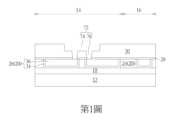
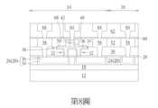
請參照第1圖至第8圖,第1圖至第8圖為本發明一實施例製作一MRAM單元之方法示意圖。如第1圖所示,首先提供一基底12,例如一由半導體材料所構成的基底12,其中半導體材料可選自由矽、鍺、矽鍺複合物、矽碳化物(silicon carbide)、砷化鎵(gallium arsenide)等所構成之群組,且基底12上較佳定義有一MRAM區域14以及一邏輯區域16。Please refer to Figures 1 to 8, which are schematic diagrams of a method for making an MRAM cell according to an embodiment of the present invention. As shown in Figure 1, a
基底12上可包含例如金氧半導體(metal-oxide semiconductor,MOS)電晶體等主動元件、被動元件、導電層以及例如層間介電層(interlayer dielectric,ILD)18等介電層覆蓋於其上。更具體而言,基底12上可包含平面型或非平面型(如鰭狀結構電晶體)等MOS電晶體元件,其中MOS電晶體可包含閘極結構(例如金屬閘極)以及源極/汲極區域、側壁子、磊晶層、接觸洞蝕刻停止層等電晶體元件,層間介電層18可設於基底12上並覆蓋MOS電晶體,且層間介電層18可具有複數個接觸插塞電連接MOS電晶體之閘極以及/或源極/汲極區域。由於平面型或非平面型電晶體與層間介電層等相關製程均為本領域所熟知技藝,在此不另加贅述。The
然後於層間介電層18上形成金屬內連線結構20電連接前述之接觸插塞,其中金屬內連線結構20包含一金屬間介電層24以及金屬內連線26鑲嵌於金屬間介電層24中。在本實施例中,金屬內連線結構20中的金屬內連線26較佳包含一溝渠導體(trench conductor),其中金屬內連線結構20中的各金屬內連線26均可依據單鑲嵌製程或雙鑲嵌製程鑲嵌於金屬間介電層24中並彼此電連接。例如各金屬內連線26可更細部包含一阻障層34以及一金屬層36,其中阻障層34可選自由鈦(Ti)、氮化鈦(TiN)、鉭(Ta)以及氮化鉭(TaN)所構成的群組,而金屬層36可選自由鎢(W)、銅(Cu)、鋁(Al)、鈦鋁合金(TiAl)、鈷鎢磷化物(cobalt tungsten phosphide,CoWP)等所構成的群組,但不侷限於此。由於單鑲嵌或雙鑲嵌製程乃本領域所熟知技藝,在此不另加贅述。Then, a
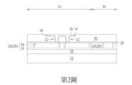
接著依序形成一停止層28以及一金屬間介電層30於金屬內連線結構20上,再進行利用一圖案化遮罩(圖未示)進行一道或以上蝕刻製程去除部分金屬間介電層30與部分停止層28以形成一開口72暴露出下方的金屬內連線表面,其中開口72較佳包含一溝渠74以及二接觸洞76連接溝渠74底部。Then, a
隨後如第2圖所示,依序形成一阻障層34以及一金屬層36於開口72內並填滿開口72,再進行一平坦化製程例如化學機械研磨(chemical mechanical polishing,CMP)製程去除部分金屬層36、部分阻障層34及部分金屬間介電層30,使剩餘的阻障層34與金屬層36頂表面切齊金屬間介電層30頂表面。值得注意的是,本階段所形成的阻障層34與金屬層36較佳同時形成一金屬內連線32以及一作為自旋軌道轉矩式(spin orbit torque,SOT)MRAM通道的自旋軌道轉矩式(SOT)層38於開口72內,其中下方填滿兩個接觸洞76的阻障層34與金屬層36較佳成為由接觸洞導體所構成的金屬內連線32而上方填滿溝渠74的阻障層34與金屬層36則較佳作為SOT層38。Subsequently, as shown in FIG. 2 , a
如同前述實施例,金屬內連線32及SOT層38中的阻障層34可選自由鈦(Ti)、氮化鈦(TiN)、鉭(Ta)以及氮化鉭(TaN)所構成的群組,而金屬層36可選自由鎢(W)、銅(Cu)、鋁(Al)、鈦鋁合金(TiAl)、鈷鎢磷化物(cobalt tungsten phosphide,CoWP)等所構成的群組,但不侷限於此。此外在本實例金屬內連線32與SOT層38中的金屬層36較佳包含鎢、金屬間介電層30較佳包含氧化矽例如四乙氧基矽烷(tetraethyl orthosilicate,TEOS)、而停止層28則包含氮摻雜碳化物層(nitrogen doped carbide,NDC)、氮化矽、或氮碳化矽(silicon carbon nitride,SiCN),但不侷限於此。As in the aforementioned embodiment, the
如第3圖所示,接著形成MTJ堆疊結構40、一硬遮罩68以及另一硬遮罩42於SOT層38上。在本實施例中,形成MTJ堆疊結構40的方式可先依序形成一固定層(pinned layer)、一阻障層(barrier layer)以及一自由層(free layer)於SOT層38上。其中固定層可包含鐵磁性材料例如但不侷限於鈷鐵硼(cobalt-iron-boron,CoFeB)、鈷鐵(cobalt-iron,CoFe)、鐵(Fe)、鈷(Co)等。此外,固定層也可以是由反鐵磁性(antiferromagnetic,AFM)材料所構成者,例如鐵錳(FeMn)、鉑錳(PtMn)、銥錳(IrMn)、氧化鎳(NiO)等,用以固定或限制鄰近層的磁矩方向。阻障層可由包含氧化物之絕緣材料所構成,例如氧化鋁(AlOx)或氧化鎂(MgO),但均不侷限於此。自由層可以是由鐵磁性材料所構成者,例如鐵、鈷、鎳或其合金如鈷鐵硼(cobalt-iron-boron,CoFeB),但不限於此。其中,自由層的磁化方向會受外部磁場而「自由」改變。另外在本實施例中,硬遮罩68較佳包含導電或金屬材料例如釕(Ru),硬遮罩42則可包含導電或介電材料例如但不侷限於鉭(Ta)、氮化鉭(TaN)、鈦(Ti)、氮化鈦(TiN)、鉑(Pt)、銅(Cu)、金(Au)、鋁(Al)或其組合。As shown in FIG. 3 , an
然後如第4圖所示,進行一蝕刻製程或更具體而言微影暨蝕刻製程圖案化硬遮罩42並暴露出下方的硬遮罩68表面。從細部來看,本階段所進行的微影暨蝕刻製程較佳先形成一圖案化遮罩(圖未示)如圖案化光阻於硬遮罩42上,然後利用圖案化遮罩為遮罩進行一蝕刻製程去除部分硬遮罩42形成圖案化之硬遮罩42並暴露出下方的部分硬遮罩68表面,其中本階段所進行的蝕刻製程較佳包含一反應性離子蝕刻(reactive ion etching,RIE)製程。Then, as shown in FIG. 4, an etching process or more specifically a lithography and etching process is performed to pattern the
隨後如第5圖所示,利用圖案化之硬遮罩42為遮罩進行一道或一道以上蝕刻製程例如離子束蝕刻(ion beam etching,IBE)製程去除部分硬遮罩68及部分MTJ堆疊結構40以形成一MTJ 48於MRAM區域14,其中部分圖案化之硬遮罩42可能在蝕刻過程中被消耗使其厚度略微降低。然後形成一遮蓋層50於MTJ 48上並覆蓋MRAM區域14以及邏輯區域16的金屬間介電層30表面。在本實施例中,遮蓋層50較佳包含氮化矽,但又可依據製程需求選用其他介電材料例如但不侷限於氧化矽、氮氧化矽或氮碳化矽。Then, as shown in FIG. 5 , one or more etching processes such as ion beam etching (IBE) are performed using the patterned
接著可在不形成任何圖案化遮罩的情況下進行一蝕刻製程去除部分遮蓋層50,其中接觸SOT層38頂表面的遮蓋層50與接觸MTJ 48側壁的遮蓋層50較佳具有不同厚度,或更具體而言SOT層38上或接觸SOT層38頂表面的遮蓋層50厚度較佳小於MTJ 48旁或接觸MTJ 48側壁的遮蓋層50厚度。Then, an etching process can be performed to remove part of the
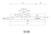
隨後如第6圖所示,可進行一微影暨蝕刻製程圖案化遮蓋層50,例如可利用一圖案化遮罩(圖未示)如圖案化光阻為遮罩進行蝕刻製程去除部分遮蓋層50並暴露出金屬間介電層30頂表面,其中被圖案化的遮蓋層50側壁可選擇切齊或不切齊下方SOT層38側壁。在本實施例中,若被圖案化的遮蓋層50側壁選擇不切齊下方SOT層38的側壁,遮蓋層50可選擇覆蓋或不覆蓋下方的SOT層38,亦即當遮蓋層50略為向外延伸或寬度大於下方SOT層38時遮蓋層50底表面可同時接觸SOT層38頂表面與金屬間介電層30頂表面,或如第6圖所示當遮蓋層50略為內縮或寬度略小於SOT層38時遮蓋層50底表面僅接觸SOT層38頂表面但不接觸金屬間介電層30頂表面,這些變化型均屬本發明所涵蓋的範圍。Subsequently, as shown in FIG. 6 , a lithography and etching process may be performed to pattern the
如第7圖所示,然後進行一沉積製程例如原子層沉積(atomic layer deposition,ALD)製程以形成一金屬間介電層52於遮蓋層50以及金屬間介電層30上,其中金屬間介電層52可包含一超低介電常數介電層,例如可包含多孔性介電材料例如但不侷限於氧碳化矽(SiOC)或氧碳化矽氫(SiOCH)。As shown in FIG. 7 , a deposition process such as atomic layer deposition (ALD) is then performed to form an
隨後可先進行一平坦化製程例如化學機械研磨(chemical mechanical polishing,CMP)製程或回蝕刻製程去除部分金屬間介電層52,使剩餘的金屬間介電層52頂表面具有平坦表面且仍略高於遮蓋層50頂表面。然後進行一圖案轉移製程,例如可利用一圖案化遮罩(圖未示)去除MRAM區域14與邏輯區域16的部分金屬間介電層52、部分金屬間介電層30及部分停止層28以形成接觸洞(圖未示)並暴露出下面的金屬內連線26。然後於接觸洞中填入所需的導電材料,例如包含鈦(Ti)、氮化鈦(TiN)、鉭(Ta)、氮化鉭(TaN)等的阻障層材料以及選自鎢(W)、銅(Cu)、鋁(Al)、鈦鋁合金(TiAl)、鈷鎢磷化物(cobalt tungsten phosphide,CoWP)等低電阻材料或其組合的低阻抗金屬層。接著進行一平坦化製程,例如以化學機械研磨製程去除部分導電材料以形成接觸插塞或金屬內連線58於接觸洞內電連接金屬內連線26。需注意的是,各金屬內連線58可包含溝渠導體設於金屬間介電層52內以及接觸洞導體設於金屬間介電層30內,其中溝渠導體底表面或接觸洞導體頂表面較佳切齊SOT層38頂表面或MTJ 48底表面。Subsequently, a planarization process such as a chemical mechanical polishing (CMP) process or an etch back process may be performed to remove a portion of the
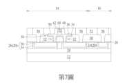
接著如第8圖所示,先形成一停止層60於MRAM區域14及邏輯區域16並覆蓋金屬間介電層52,形成一金屬間介電層62於停止層60上,進行一道或一道以上微影暨蝕刻製程去除MRAM區域14及邏輯區域16的部分金屬間介電層62、部分停止層60、部分金屬間介電層52以及部分遮蓋層50形成接觸洞(圖未示)。接著填入導電材料於各接觸洞內並搭配平坦化製程如CMP以分別於MRAM區域14以及邏輯區域16形成金屬內連線64電連接下方的MTJ 48及金屬內連線58,其中MRAM區域14的金屬內連線64較佳直接接觸設於下方的硬遮罩42而邏輯區域16的金屬內連線64則接觸下層的金屬內連線58。Next, as shown in FIG. 8 , a
在本實施例中,停止層60與停止層28可包含相同或不同材料,其中兩者均可選自由氮摻雜碳化物層(nitrogen doped carbide,NDC)、氮化矽、以及氮碳化矽(silicon carbon nitride,SiCN)所構成的群組。如同前述所形成的金屬內連線,設於金屬間介電層62內的金屬內連線64可依據單鑲嵌製程或雙鑲嵌製程鑲嵌於金屬間介電層62內。例如金屬內連線64可更細部包含一阻障層以及一金屬層,其中阻障層可選自由鈦(Ti)、氮化鈦(TiN)、鉭(Ta)以及氮化鉭(TaN)所構成的群組,而金屬層可選自由鎢(W)、銅(Cu)、鋁(Al)、鈦鋁合金(TiAl)、鈷鎢磷化物(cobalt tungsten phosphide,CoWP)等所構成的群組,但不侷限於此。由於單鑲嵌或雙鑲嵌製程乃本領域所熟知技藝,在此不另加贅述。至此即完成本發明一實施例之半導體元件的製作。In this embodiment, the
請參照第9圖至第11圖,第9圖至第11圖為本發明一實施例製作一MRAM單元之方法示意圖。如第9圖所示,首先比照第1圖先形成層間介電層18於基底12上,然後於層間介電層18上依序形成金屬內連線結構20、22電連接層間介電層18內的接觸插塞,其中金屬內連線結構20包含一金屬間介電層24以及金屬內連線26鑲嵌於金屬間介電層24中,金屬內連線結構22則包含一停止層28、一金屬間介電層30以及至少二金屬內連線32鑲嵌於停止層28與金屬間介電層30中。Please refer to Figures 9 to 11, which are schematic diagrams of a method for manufacturing an MRAM cell according to an embodiment of the present invention. As shown in Figure 9, first, an
在本實施例中,金屬內連線結構20中的各金屬內連線26較佳包含一溝渠導體(trench conductor),金屬內連線結構22中設於MRAM區域14的的金屬內連線32則包含接觸洞導體(via conductor)設於二接觸洞內。另外各金屬內連線結構20、22中的各金屬內連線26、32均可依據單鑲嵌製程或雙鑲嵌製程鑲嵌於金屬間介電層24、30以及/或停止層28中並彼此電連接。例如各金屬內連線26、32可更細部包含一阻障層34以及一金屬層36,其中阻障層34可選自由鈦(Ti)、氮化鈦(TiN)、鉭(Ta)以及氮化鉭(TaN)所構成的群組,而金屬層36可選自由鎢(W)、銅(Cu)、鋁(Al)、鈦鋁合金(TiAl)、鈷鎢磷化物(cobalt tungsten phosphide,CoWP)等所構成的群組,但不侷限於此。由於單鑲嵌或雙鑲嵌製程乃本領域所熟知技藝,在此不另加贅述。此外在本實例金屬內連線26中的金屬層36較佳包含銅、金屬內連線32中的金屬層36較佳包含鎢、金屬間介電層24、30較佳包含氧化矽例如四乙氧基矽烷(tetraethyl orthosilicate,TEOS)、而停止層28則包含氮摻雜碳化物層(nitrogen doped carbide,NDC)、氮化矽、或氮碳化矽(silicon carbon nitride,SiCN),但不侷限於此。接著形成另一金屬間介電層78於金屬內連線結構22上,並進行一微影暨蝕刻製程去除部分金屬間介電層78以形成一開口80或溝渠暴露出下方的金屬內連線32。In this embodiment, each
如第10圖所示,接著依序形成一阻障層34以及一金屬層36於開口80內並填滿開口80,再進行一平坦化製程例如化學機械研磨(chemical mechanical polishing,CMP)製程去除部分阻障層34、部分金屬層36及部分金屬間介電層78,使剩餘的阻障層34與金屬層36頂表面切齊金屬間介電層78頂表面並形成一自旋軌道轉矩式(spin orbit torque,SOT)層38於開口80內。As shown in FIG. 10 , a
如同前述實施例,SOT層38較佳作為一自旋軌道轉矩式(SOT)MRAM之通道,其中的阻障層34可選自由鈦(Ti)、氮化鈦(TiN)、鉭(Ta)以及氮化鉭(TaN)所構成的群組,而金屬層36則可包含鉭(Ta)、鎢(W)、鉑(Pt)、鉿(Hf)、硒化鉍(BixSe1-x)或其組合。需注意的是,相較於前述實施例中金屬內連線32與SOT層38中的金屬層36較佳由相同金屬材料如鎢所構成,本實施例中金屬內連線32與SOT層38中的金屬層36可依據產品需求由相同或不同材料所構成。在本實例中,金屬內連線32與SOT層38中的金屬層36均較佳包含鎢,金屬間介電層24、30、78較佳包含氧化矽例如四乙氧基矽烷(tetraethyl orthosilicate,TEOS),但不侷限於此。As in the above-mentioned embodiment, the
隨後如第11圖所示,比照前述第3圖至第8圖的製程先形成MTJ堆疊結構40、硬遮罩68以及另一硬遮罩42於SOT層38上,圖案化硬遮罩42、硬遮罩68以及MTJ堆疊結構40形成MTJ 48,形成遮蓋層50於MTJ 48上,圖案化遮蓋層50使遮蓋層50邊緣切齊或不切齊下方的SOT層38側壁,形成金屬間介電層52於遮蓋層50上,形成金屬內連線58於金屬間介電層52、金屬間介電層78以及金屬間介電層30內連接下方的金屬內連線26,形成停止層60及金屬間介電層62於金屬間介電層52上,最後再形成金屬內連線64於金屬間介電層62內電連接下方的MTJ 48及金屬內連線58,其中MRAM區域14的金屬內連線64直接接觸設於下方的硬遮罩42而邏輯區域16的金屬內連線64則接觸下層的金屬內連線58。Then, as shown in FIG. 11, the
以上所述僅為本發明之較佳實施例,凡依本發明申請專利範圍所做之均等變化與修飾,皆應屬本發明之涵蓋範圍。The above is only the preferred embodiment of the present invention. All equivalent changes and modifications made within the scope of the patent application of the present invention shall fall within the scope of the present invention.
12:基底 14:MRAM區域 16:邏輯區域 18:層間介電層 20:金屬內連線結構 24:金屬間介電層 26:金屬內連線 28:停止層 30:金屬間介電層 32:金屬內連線 34:阻障層 36:金屬層 38:SOT層 42:硬遮罩 48:MTJ 50:遮蓋層 52:金屬間介電層 58:金屬內連線 60:停止層 62:金屬間介電層 64:金屬內連線 68:硬遮罩12: substrate14: MRAM area16: logic area18: interlayer dielectric layer20: metal interconnect structure24: intermetal dielectric layer26: metal interconnect28: stop layer30: intermetal dielectric layer32: metal interconnect34: barrier layer36: metal layer38: SOT layer42: hard mask48: MTJ50: cover layer52: intermetal dielectric layer58: metal interconnect60: stop layer62: intermetal dielectric layer64: metal interconnect68: hard mask
Claims (14)
Translated fromChineseApplications Claiming Priority (2)
| Application Number | Priority Date | Filing Date | Title |
|---|---|---|---|
| CN202210298345.4ACN116867349A (en) | 2022-03-24 | 2022-03-24 | Semiconductor element and manufacturing method thereof |
| CN202210298345.4 | 2022-03-24 |
Publications (2)
| Publication Number | Publication Date |
|---|---|
| TW202339314A TW202339314A (en) | 2023-10-01 |
| TWI886405Btrue TWI886405B (en) | 2025-06-11 |
Family
ID=88193027
Family Applications (1)
| Application Number | Title | Priority Date | Filing Date |
|---|---|---|---|
| TW111130587ATWI886405B (en) | 2022-03-24 | 2022-08-15 | Semiconductor device and method for fabricating the same |
Country Status (3)
| Country | Link |
|---|---|
| US (1) | US12389808B2 (en) |
| CN (1) | CN116867349A (en) |
| TW (1) | TWI886405B (en) |
Citations (4)
| Publication number | Priority date | Publication date | Assignee | Title |
|---|---|---|---|---|
| US20200006631A1 (en)* | 2018-06-29 | 2020-01-02 | Intel Corporation | Spin orbit torque (sot) memory devices and methods of fabrication |
| US20200227626A1 (en)* | 2019-01-14 | 2020-07-16 | Samsung Electronics Co., Ltd. | Semiconductor devices including spin-orbit torque line and contact plug |
| US20210098693A1 (en)* | 2019-09-26 | 2021-04-01 | Taiwan Semiconductor Manufacturing Co., Ltd. | Memory device and method for manufacturing the same |
| TW202118101A (en)* | 2019-10-30 | 2021-05-01 | 台灣積體電路製造股份有限公司 | Magnetic memory device, magnetic memory and method of forming the same |
Family Cites Families (3)
| Publication number | Priority date | Publication date | Assignee | Title |
|---|---|---|---|---|
| WO2014025838A1 (en) | 2012-08-06 | 2014-02-13 | Cornell University | Electrically gated three-terminal circuits and devices based on spin hall torque effects in magnetic nanostructures |
| US11469268B2 (en)* | 2016-03-18 | 2022-10-11 | Intel Corporation | Damascene-based approaches for embedding spin hall MTJ devices into a logic processor and the resulting structures |
| US11062752B2 (en)* | 2019-01-11 | 2021-07-13 | Intel Corporation | Spin orbit torque memory devices and methods of fabrication |
- 2022
- 2022-03-24CNCN202210298345.4Apatent/CN116867349A/enactivePending
- 2022-04-19USUS17/723,495patent/US12389808B2/enactiveActive
- 2022-08-15TWTW111130587Apatent/TWI886405B/enactive
Patent Citations (4)
| Publication number | Priority date | Publication date | Assignee | Title |
|---|---|---|---|---|
| US20200006631A1 (en)* | 2018-06-29 | 2020-01-02 | Intel Corporation | Spin orbit torque (sot) memory devices and methods of fabrication |
| US20200227626A1 (en)* | 2019-01-14 | 2020-07-16 | Samsung Electronics Co., Ltd. | Semiconductor devices including spin-orbit torque line and contact plug |
| US20210098693A1 (en)* | 2019-09-26 | 2021-04-01 | Taiwan Semiconductor Manufacturing Co., Ltd. | Memory device and method for manufacturing the same |
| TW202118101A (en)* | 2019-10-30 | 2021-05-01 | 台灣積體電路製造股份有限公司 | Magnetic memory device, magnetic memory and method of forming the same |
Also Published As
| Publication number | Publication date |
|---|---|
| TW202339314A (en) | 2023-10-01 |
| US20230320232A1 (en) | 2023-10-05 |
| CN116867349A (en) | 2023-10-10 |
| US12389808B2 (en) | 2025-08-12 |
Similar Documents
| Publication | Publication Date | Title |
|---|---|---|
| CN112447788B (en) | magnetoresistive random access memory | |
| CN111969103B (en) | Semiconductor components and manufacturing methods | |
| CN112968036B (en) | Semiconductor element and manufacturing method thereof | |
| CN111106235B (en) | Semiconductor element and manufacturing method thereof | |
| CN111916472B (en) | magnetoresistive random access memory | |
| CN110890460A (en) | Semiconductor device and method of making the same | |
| CN114447023A (en) | Semiconductor element and manufacturing method thereof | |
| US20240237553A1 (en) | Semiconductor device and method for fabricating the same | |
| CN115440881A (en) | Semiconductor element and manufacturing method thereof | |
| CN113571465A (en) | Semiconductor element and manufacturing method thereof | |
| TW202123501A (en) | Semiconductor device and method for fabricating the same | |
| CN116981340A (en) | Semiconductor element and manufacturing method thereof | |
| CN116267013A (en) | Semiconductor element and manufacturing method thereof | |
| CN115811925A (en) | Semiconductor element and manufacturing method thereof | |
| CN112420918B (en) | Semiconductor element and manufacturing method thereof | |
| CN113972315A (en) | Semiconductor element and manufacturing method thereof | |
| CN114335331A (en) | Semiconductor element and manufacturing method thereof | |
| CN113594086A (en) | Semiconductor element and manufacturing method thereof | |
| CN113594087A (en) | Semiconductor element and manufacturing method thereof | |
| CN111477738A (en) | A method of making a semiconductor element | |
| TW202329493A (en) | Semiconductor device and method for fabricating the same | |
| CN116156995A (en) | Semiconductor structure and manufacturing method thereof | |
| TWI886405B (en) | Semiconductor device and method for fabricating the same | |
| CN115377283A (en) | Magnetoresistive random access memory | |
| TWI884381B (en) | Method for fabricating magnetoresistive random access memory |