TWI882595B - Semiconductor device and manufacturing method thereof - Google Patents
Semiconductor device and manufacturing method thereofDownload PDFInfo
- Publication number
- TWI882595B TWI882595BTW112149963ATW112149963ATWI882595BTW I882595 BTWI882595 BTW I882595BTW 112149963 ATW112149963 ATW 112149963ATW 112149963 ATW112149963 ATW 112149963ATW I882595 BTWI882595 BTW I882595B
- Authority
- TW
- Taiwan
- Prior art keywords
- oxide semiconductor
- layer
- semiconductor layer
- region
- oxide
- Prior art date
Links
Images


Classifications
- H—ELECTRICITY
- H10—SEMICONDUCTOR DEVICES; ELECTRIC SOLID-STATE DEVICES NOT OTHERWISE PROVIDED FOR
- H10D—INORGANIC ELECTRIC SEMICONDUCTOR DEVICES
- H10D30/00—Field-effect transistors [FET]
- H10D30/60—Insulated-gate field-effect transistors [IGFET]
- H10D30/67—Thin-film transistors [TFT]
- H10D30/674—Thin-film transistors [TFT] characterised by the active materials
- H10D30/6755—Oxide semiconductors, e.g. zinc oxide, copper aluminium oxide or cadmium stannate
- H—ELECTRICITY
- H01—ELECTRIC ELEMENTS
- H01L—SEMICONDUCTOR DEVICES NOT COVERED BY CLASS H10
- H01L21/00—Processes or apparatus adapted for the manufacture or treatment of semiconductor or solid state devices or of parts thereof
- H01L21/02—Manufacture or treatment of semiconductor devices or of parts thereof
- H01L21/02104—Forming layers
- H01L21/02365—Forming inorganic semiconducting materials on a substrate
- H01L21/02518—Deposited layers
- H01L21/02521—Materials
- H01L21/02551—Group 12/16 materials
- H01L21/02554—Oxides
- H—ELECTRICITY
- H01—ELECTRIC ELEMENTS
- H01L—SEMICONDUCTOR DEVICES NOT COVERED BY CLASS H10
- H01L21/00—Processes or apparatus adapted for the manufacture or treatment of semiconductor or solid state devices or of parts thereof
- H01L21/02—Manufacture or treatment of semiconductor devices or of parts thereof
- H01L21/02104—Forming layers
- H01L21/02365—Forming inorganic semiconducting materials on a substrate
- H01L21/02518—Deposited layers
- H01L21/02521—Materials
- H01L21/02565—Oxide semiconducting materials not being Group 12/16 materials, e.g. ternary compounds
- H—ELECTRICITY
- H01—ELECTRIC ELEMENTS
- H01L—SEMICONDUCTOR DEVICES NOT COVERED BY CLASS H10
- H01L21/00—Processes or apparatus adapted for the manufacture or treatment of semiconductor or solid state devices or of parts thereof
- H01L21/02—Manufacture or treatment of semiconductor devices or of parts thereof
- H01L21/02104—Forming layers
- H01L21/02365—Forming inorganic semiconducting materials on a substrate
- H01L21/02612—Formation types
- H01L21/02617—Deposition types
- H01L21/02631—Physical deposition at reduced pressure, e.g. MBE, sputtering, evaporation
- H—ELECTRICITY
- H10—SEMICONDUCTOR DEVICES; ELECTRIC SOLID-STATE DEVICES NOT OTHERWISE PROVIDED FOR
- H10D—INORGANIC ELECTRIC SEMICONDUCTOR DEVICES
- H10D30/00—Field-effect transistors [FET]
- H10D30/01—Manufacture or treatment
- H10D30/021—Manufacture or treatment of FETs having insulated gates [IGFET]
- H10D30/031—Manufacture or treatment of FETs having insulated gates [IGFET] of thin-film transistors [TFT]
- H—ELECTRICITY
- H10—SEMICONDUCTOR DEVICES; ELECTRIC SOLID-STATE DEVICES NOT OTHERWISE PROVIDED FOR
- H10D—INORGANIC ELECTRIC SEMICONDUCTOR DEVICES
- H10D30/00—Field-effect transistors [FET]
- H10D30/60—Insulated-gate field-effect transistors [IGFET]
- H10D30/67—Thin-film transistors [TFT]
- H10D30/6729—Thin-film transistors [TFT] characterised by the electrodes
- H10D30/673—Thin-film transistors [TFT] characterised by the electrodes characterised by the shapes, relative sizes or dispositions of the gate electrodes
- H10D30/6733—Multi-gate TFTs
- H10D30/6734—Multi-gate TFTs having gate electrodes arranged on both top and bottom sides of the channel, e.g. dual-gate TFTs
- H—ELECTRICITY
- H10—SEMICONDUCTOR DEVICES; ELECTRIC SOLID-STATE DEVICES NOT OTHERWISE PROVIDED FOR
- H10D—INORGANIC ELECTRIC SEMICONDUCTOR DEVICES
- H10D30/00—Field-effect transistors [FET]
- H10D30/60—Insulated-gate field-effect transistors [IGFET]
- H10D30/67—Thin-film transistors [TFT]
- H10D30/6729—Thin-film transistors [TFT] characterised by the electrodes
- H10D30/6737—Thin-film transistors [TFT] characterised by the electrodes characterised by the electrode materials
- H10D30/6739—Conductor-insulator-semiconductor electrodes
- H—ELECTRICITY
- H10—SEMICONDUCTOR DEVICES; ELECTRIC SOLID-STATE DEVICES NOT OTHERWISE PROVIDED FOR
- H10D—INORGANIC ELECTRIC SEMICONDUCTOR DEVICES
- H10D30/00—Field-effect transistors [FET]
- H10D30/60—Insulated-gate field-effect transistors [IGFET]
- H10D30/67—Thin-film transistors [TFT]
- H10D30/674—Thin-film transistors [TFT] characterised by the active materials
- H10D30/6755—Oxide semiconductors, e.g. zinc oxide, copper aluminium oxide or cadmium stannate
- H10D30/6756—Amorphous oxide semiconductors
- H—ELECTRICITY
- H10—SEMICONDUCTOR DEVICES; ELECTRIC SOLID-STATE DEVICES NOT OTHERWISE PROVIDED FOR
- H10D—INORGANIC ELECTRIC SEMICONDUCTOR DEVICES
- H10D30/00—Field-effect transistors [FET]
- H10D30/60—Insulated-gate field-effect transistors [IGFET]
- H10D30/67—Thin-film transistors [TFT]
- H10D30/6757—Thin-film transistors [TFT] characterised by the structure of the channel, e.g. transverse or longitudinal shape or doping profile
- H—ELECTRICITY
- H10—SEMICONDUCTOR DEVICES; ELECTRIC SOLID-STATE DEVICES NOT OTHERWISE PROVIDED FOR
- H10D—INORGANIC ELECTRIC SEMICONDUCTOR DEVICES
- H10D62/00—Semiconductor bodies, or regions thereof, of devices having potential barriers
- H10D62/40—Crystalline structures
- H—ELECTRICITY
- H10—SEMICONDUCTOR DEVICES; ELECTRIC SOLID-STATE DEVICES NOT OTHERWISE PROVIDED FOR
- H10D—INORGANIC ELECTRIC SEMICONDUCTOR DEVICES
- H10D62/00—Semiconductor bodies, or regions thereof, of devices having potential barriers
- H10D62/40—Crystalline structures
- H10D62/402—Amorphous materials
- H—ELECTRICITY
- H10—SEMICONDUCTOR DEVICES; ELECTRIC SOLID-STATE DEVICES NOT OTHERWISE PROVIDED FOR
- H10D—INORGANIC ELECTRIC SEMICONDUCTOR DEVICES
- H10D62/00—Semiconductor bodies, or regions thereof, of devices having potential barriers
- H10D62/40—Crystalline structures
- H10D62/405—Orientations of crystalline planes
- H—ELECTRICITY
- H10—SEMICONDUCTOR DEVICES; ELECTRIC SOLID-STATE DEVICES NOT OTHERWISE PROVIDED FOR
- H10D—INORGANIC ELECTRIC SEMICONDUCTOR DEVICES
- H10D62/00—Semiconductor bodies, or regions thereof, of devices having potential barriers
- H10D62/80—Semiconductor bodies, or regions thereof, of devices having potential barriers characterised by the materials
- H10D62/86—Semiconductor bodies, or regions thereof, of devices having potential barriers characterised by the materials being Group II-VI materials, e.g. ZnO
- H10D62/862—Semiconductor bodies, or regions thereof, of devices having potential barriers characterised by the materials being Group II-VI materials, e.g. ZnO being Group II-VI materials comprising three or more elements, e.g. CdZnTe
- H—ELECTRICITY
- H10—SEMICONDUCTOR DEVICES; ELECTRIC SOLID-STATE DEVICES NOT OTHERWISE PROVIDED FOR
- H10D—INORGANIC ELECTRIC SEMICONDUCTOR DEVICES
- H10D64/00—Electrodes of devices having potential barriers
- H10D64/20—Electrodes characterised by their shapes, relative sizes or dispositions
- H10D64/27—Electrodes not carrying the current to be rectified, amplified, oscillated or switched, e.g. gates
- H10D64/311—Gate electrodes for field-effect devices
- H10D64/411—Gate electrodes for field-effect devices for FETs
- H10D64/511—Gate electrodes for field-effect devices for FETs for IGFETs
- H10D64/512—Disposition of the gate electrodes, e.g. buried gates
- H—ELECTRICITY
- H10—SEMICONDUCTOR DEVICES; ELECTRIC SOLID-STATE DEVICES NOT OTHERWISE PROVIDED FOR
- H10D—INORGANIC ELECTRIC SEMICONDUCTOR DEVICES
- H10D64/00—Electrodes of devices having potential barriers
- H10D64/60—Electrodes characterised by their materials
- H10D64/62—Electrodes ohmically coupled to a semiconductor
- H—ELECTRICITY
- H10—SEMICONDUCTOR DEVICES; ELECTRIC SOLID-STATE DEVICES NOT OTHERWISE PROVIDED FOR
- H10D—INORGANIC ELECTRIC SEMICONDUCTOR DEVICES
- H10D99/00—Subject matter not provided for in other groups of this subclass
Landscapes
- Engineering & Computer Science (AREA)
- Physics & Mathematics (AREA)
- Condensed Matter Physics & Semiconductors (AREA)
- General Physics & Mathematics (AREA)
- Manufacturing & Machinery (AREA)
- Computer Hardware Design (AREA)
- Microelectronics & Electronic Packaging (AREA)
- Power Engineering (AREA)
- Thin Film Transistor (AREA)
- Chemical & Material Sciences (AREA)
- Crystallography & Structural Chemistry (AREA)
- Electrodes Of Semiconductors (AREA)
- Metal-Oxide And Bipolar Metal-Oxide Semiconductor Integrated Circuits (AREA)
- Recrystallisation Techniques (AREA)
- Dram (AREA)
- Physical Deposition Of Substances That Are Components Of Semiconductor Devices (AREA)
- Liquid Crystal (AREA)
- Encapsulation Of And Coatings For Semiconductor Or Solid State Devices (AREA)
Abstract
Description
Translated fromChinese本發明係關於包含氧化物半導體的半導體裝置及其製造方法。此處,半導體裝置意指利用半導體特徵操作的所有元件裝置。舉例而言,在半導體裝置的類別中廣泛地包含電力裝置、閘流體、轉換器、影像感測器、記憶體、等等;包含這些裝置的半導體積體電路;以液晶顯示面板為代表的電光裝置;包含有機發光元件的發光顯示裝置;等等。The present invention relates to a semiconductor device including an oxide semiconductor and a method for manufacturing the same. Here, semiconductor devices refer to all device components that utilize semiconductor characteristics to operate. For example, the category of semiconductor devices broadly includes power devices, gates, converters, image sensors, memories, etc.; semiconductor integrated circuits including these devices; electro-optical devices represented by liquid crystal display panels; light-emitting display devices including organic light-emitting elements; etc.
場效電晶體是最廣泛使用的半導體元件。根據場效電晶體的用途,以各種不同的材料用於這些場效電晶體。特別地,經常使用包含矽的半導體材料。Field effect transistors are the most widely used semiconductor components. Various materials are used for these field effect transistors depending on the purpose of the field effect transistors. In particular, semiconductor materials containing silicon are often used.
包含矽的場效電晶體具有滿足不同用途所需的特徵。舉例而言,單晶矽用於需要高速操作的積體電路等等,因而滿足高速操作之需求。此外,以非晶矽用於例如顯示裝置等需要大面積的裝置,因而滿足大面積的需求。Field effect transistors containing silicon have characteristics that meet the requirements of different uses. For example, single-crystal silicon is used in integrated circuits that require high-speed operation, thereby meeting the requirements of high-speed operation. In addition, amorphous silicon is used in devices that require large areas, such as display devices, thereby meeting the requirements of large areas.
如上所述,矽是高度多樣的且用於各種不同目的。但是,近年來期望半導體材料具有更高的性能及多樣性。舉例而言,以增進大面積顯示裝置的性能的觀點而言,為了實現切換元件的高速操作,需要有利於增加顯示裝置的面積及比非晶矽呈現更高性能的半導體材料。As mentioned above, silicon is highly diverse and is used for a variety of different purposes. However, in recent years, semiconductor materials are expected to have higher performance and diversity. For example, from the perspective of improving the performance of large-area display devices, in order to achieve high-speed operation of switching elements, semiconductor materials that are conducive to increasing the area of display devices and exhibiting higher performance than amorphous silicon are required.
某些金屬氧化物具有半導體特徵,舉例而言,已知氧化鎢、氧化錫、氧化銦、氧化鋅、等等。已知使用具有半導體特徵的此類金屬氧化物以形成通道形成區之薄膜電晶體。(請參見專利文獻1至4及非專利文獻1)。Some metal oxides have semiconductor characteristics, for example, tungsten oxide, tin oxide, indium oxide, zinc oxide, etc. are known. It is known to use such metal oxides having semiconductor characteristics to form a thin film transistor having a channel formation region. (See
關於金屬氧化物,已知不僅有單一成分氧化物,也有多成分氧化物。舉例而言,已知具有同系性之InGaO3(ZnO)m(m是自然數)是包含In、Ga、及Zn之多成分氧化物半導體(非專利文獻2至4)。As for metal oxides, it is known that there are not only single-component oxides but also multi-component oxides. For example, it is known that InGaO3 (ZnO)m (m is a natural number) having homology is a multi-component oxide semiconductor containing In, Ga, and Zn (
在這些條件下,使用氧化物半導體之場效電晶體(也稱為FET)有關的技術引起注意。此外,已確認包含此In-Ga-Zn-O為基礎的氧化物之氧化物半導體可以應用於薄膜電晶體的通道層(舉例而言,請參見非專利文獻5和6)。Under these conditions, technologies related to field effect transistors (also called FETs) using oxide semiconductors have attracted attention. In addition, it has been confirmed that oxide semiconductors containing this In-Ga-Zn-O-based oxide can be applied to the channel layer of thin film transistors (for example, see
舉例而言,在專利文獻5中,揭示使用同系化合物InMO3(ZnO)m(M是In、Fe、Ga、或Al,m是大於或等於1且低於50的整數)的透明薄膜場效電晶體。For example,
此外,在專利文獻6中,揭示的場效電晶體使用含有In、Ga、及Zn且具有小於1018/cm3的電子載子濃度的非晶氧化物半導體。注意,在此專利文獻中,在非晶氧化物半導體中In原子相對於Ga原子及Zn原子的比例以In:Ga:Zn=1:1:m(m<6)表示。In addition, in
此外,在專利文獻7中,揭示的場效電晶體中以包含微晶的非晶氧化物半導體用於主動層。In addition, in
[專利文獻1]日本公開專利申請號S60-198861[Patent document 1] Japanese published patent application number S60-198861
[專利文獻2]日本公開專利申請號H8-264794[Patent Document 2] Japanese Patent Application No. H8-264794
[專利文獻3]PCT國際申請號H11-505377之日文譯本[Patent Document 3] Japanese translation of PCT international application number H11-505377
[專利文獻4]日本公開專利申請號2000-150900[Patent Document 4] Japanese Patent Application No. 2000-150900
[專利文獻5]日本公開專利申請號2004-103957[Patent Document 5] Japanese Patent Application No. 2004-103957
[專利文獻6]PCT公告號05/088726[Patent Document 6] PCT Publication No. 05/088726
[專利文獻7]日本公開專利申請號2006-165529[Patent Document 7] Japanese Patent Application No. 2006-165529
[非專利文獻1]M. W. Prins, K.O. Grosse-Holz, G. Muller, J.F.M. Cillessen, J.B. Giesbers, R.P. Weening, and R. M. Wolf, “A ferroelectric transparent thin-film transistor”, Appl. Phys. Lett., 17 June 1996, Vol.68 pp. 3650-3652[Non-patent document 1] M. W. Prins, K.O. Grosse-Holz, G. Muller, J.F.M. Cillessen, J.B. Giesbers, R.P. Weening, and R. M. Wolf, “A ferroelectric transparent thin-film transistor”, Appl. Phys. Lett., 17 June 1996, Vol.68 pp. 3650-3652
[非專利文獻2]M. Nakamura, N.Kimizuka, and T. Mohri, “The phase Relations in the In2O3-Ga2ZnO4-ZnO System at 1350℃”, J. Solid State Chem., 1991, Vol.93, pp. 298-315[Non-patent document 2] M. Nakamura, N.Kimizuka, and T. Mohri, “The phase Relations in the In2 O3 -Ga2 ZnO4 -ZnO System at 1350℃”, J. Solid State Chem., 1991, Vol.93, pp. 298-315
[非專利文獻3]N. Kimizuka, M. Isobe, and M. Nakamura, “Syntheses and Single-Crystal Data of Homologousj Compounds, In2O3(ZnO)m(m=3, 4, and 5), InGaO3(ZnO)3, and Ga2O3(ZnO)m (m=7, 8, 9, and 16) in the In2O3-ZnGa2O4-ZnO System”, J. Solid State Chem., 1995, Vol. 116, pp. 170-178[Non-patent document 3] N. Kimizuka, M. Isobe, and M. Nakamura, “Syntheses and Single-Crystal Data of Homologousj Compounds, In2 O3 (ZnO)m (m=3, 4, and 5), InGaO3 (ZnO)3 , and Ga2 O3 (ZnO)m (m=7, 8, 9, and 16) in the In2 O3 -ZnGa2 O4 -ZnO System”, J. Solid State Chem., 1995, Vol. 116, pp. 170-178
[非專利文獻4]M. Nakamura, N.Kimizuka, T. Mohri, and M. Isobe, “Homologous Series, Synthesis and Crystal Structure of InFeO3(ZnO)m (m:natural number) and its Isostructural Compound”,KOTAI BUTSURI(Solid State PHYSICS), 1993, Vol.28, pp. 317-327[Non-patent document 4] M. Nakamura, N.Kimizuka, T. Mohri, and M. Isobe, "Homologous Series, Synthesis and Crystal Structure of InFeO3 (ZnO)m (m: natural number) and its Isostructural Compound", KOTAI BUTSURI (Solid State PHYSICS), 1993, Vol.28, pp. 317-327
[非專利文獻5]K. Nomura, H. Ohta, K. Ueda, T. Kamiya, M. Hirano, and H. Hosono, “Thin-film transistor fabricated in single-crystalline transparent oxide semiconductor”, SCIENCE, 2003, Vol. 300, pp. 1269-1272[Non-patent document 5] K. Nomura, H. Ohta, K. Ueda, T. Kamiya, M. Hirano, and H. Hosono, “Thin-film transistor fabricated in single-crystalline transparent oxide semiconductor”, SCIENCE, 2003, Vol. 300, pp. 1269-1272
[非專利文獻6]K. Nomura, H.Ohta, A. Takagi, T. Kamiya, M. Hirano, and H.Hosono, “Room-temperature fabrication of transparent flexible thin-film transistors using amorphous oxide semiconductors”, NATURE, 2004, Vol.432 pp. 488-492[Non-patent document 6] K. Nomura, H.Ohta, A. Takagi, T. Kamiya, M. Hirano, and H.Hosono, “Room-temperature fabrication of transparent flexible thin-film transistors using amorphous oxide semiconductors”, NATURE, 2004, Vol.432 pp. 488-492
在專利文獻3中,揭示晶體狀態的成分為InGaO3(ZnO)m(m是小於6的整數)。此外,在專利文獻3的實施例1中,揭示InGaO3(ZnO)4的情形。但是,即使使用這些氧化物半導體時,事實上仍然尚未取得適當的特徵。
慮及上述問題,目的在於提供具有使用具有新穎結構的氧化物半導體層之新穎結構的半導體裝置。In view of the above problems, an object is to provide a semiconductor device having a novel structure using an oxide semiconductor layer having a novel structure.
在揭示的發明中,使用經過純化的包含結晶區之氧化物半導體層,形成半導體裝置。舉例而言,結晶區是具有電各向異性的區域或是防止雜質進入的區域。In the disclosed invention, a semiconductor device is formed using a purified oxide semiconductor layer including a crystallized region. For example, the crystallized region is a region having electrical anisotropy or a region that prevents entry of impurities.
揭示的發明之實施例是半導體裝置,其包含:第一氧化物半導體層,包括在具有絕緣表面的基底上從第一氧化物半導體層的表面朝向內部生長形成的結晶區;在第一氧化物半導體層上的第二氧化物半導體層;與第二氧化物半導體層接觸的源極電極層和汲極電極層;閘極絕緣層,遮蓋第二氧化物半導體層、源極電極層、和汲極電極層;以及,在閘極絕緣層上且在與第二氧化物半導體層重疊的區域中的閘極電極層。第二氧化物半導體層是包含從結晶區生長形成的晶體之層。An embodiment of the disclosed invention is a semiconductor device, comprising: a first oxide semiconductor layer including a crystallization region formed by growing from a surface of the first oxide semiconductor layer toward the inside on a substrate having an insulating surface; a second oxide semiconductor layer on the first oxide semiconductor layer; a source electrode layer and a drain electrode layer in contact with the second oxide semiconductor layer; a gate insulating layer covering the second oxide semiconductor layer, the source electrode layer, and the drain electrode layer; and a gate electrode layer on the gate insulating layer and in a region overlapping with the second oxide semiconductor layer. The second oxide semiconductor layer is a layer including crystals grown from the crystallization region.
揭示的發明之另一實施例是半導體裝置,其包含:在具有絕緣表面的基底上的第一閘極電極層;遮蓋第一閘極電極層的第一閘極絕緣層;第一氧化物半導體層,包括在第一閘極絕緣層上從第一氧化物半導體層的表面朝向內部生長形成的結晶區;在第一氧化物半導體層上的第二氧化物半導體層;與第二氧化物半導體層接觸的源極電極層和汲極電極層;第二閘極絕緣層,遮蓋第二氧化物半導體層、源極電極層、和汲極電極層;以及,在第二閘極絕緣層上且在與第二氧化物半導體層重疊的區域中的閘極電極層。第二氧化物半導體層是包含從結晶區生長形成的晶體之層。Another embodiment of the disclosed invention is a semiconductor device, comprising: a first gate electrode layer on a substrate having an insulating surface; a first gate insulating layer covering the first gate electrode layer; a first oxide semiconductor layer, including a crystallized region grown from the surface of the first oxide semiconductor layer toward the inside on the first gate insulating layer; a second oxide semiconductor layer on the material semiconductor layer; a source electrode layer and a drain electrode layer in contact with the second oxide semiconductor layer; a second gate insulating layer covering the second oxide semiconductor layer, the source electrode layer, and the drain electrode layer; and a gate electrode layer on the second gate insulating layer and in a region overlapping with the second oxide semiconductor layer. The second oxide semiconductor layer is a layer including a crystal grown from a crystallization region.
在上述半導體裝置的結構中,在與閘極電極層重疊的區域(通道形成區)中,第二氧化物半導體層的表面高度的變異是1nm或更少(較佳地,0.2nm或更低)。In the structure of the above-mentioned semiconductor device, in the region overlapping with the gate electrode layer (channel formation region), the variation in the surface height of the second oxide semiconductor layer is 1 nm or less (preferably, 0.2 nm or less).
注意,第一氧化物半導體層的結晶區具有在垂直於第一氧化物半導體層的表面之方向上對齊的c軸。此外,晶體的c軸相當於膜厚方向。Note that the crystal region of the first oxide semiconductor layer has a c-axis aligned in a direction perpendicular to the surface of the first oxide semiconductor layer. In addition, the c-axis of the crystal is equivalent to the film thickness direction.
在上述半導體裝置的結構中,具有絕緣表面的基底包含氧化物或氮化物。In the structure of the above-mentioned semiconductor device, the substrate having an insulating surface includes oxide or nitride.
在上述半導體裝置的結構中,包含於第一氧化物半導體層中的結晶區具有大於或等於2nm且小於或等於10nm的平均厚度。In the structure of the above-mentioned semiconductor device, the crystallized region included in the first oxide semiconductor layer has an average thickness greater than or equal to 2 nm and less than or equal to 10 nm.
在上述半導體裝置的結構中,第一氧化物半導體層或第二氧化物半導體層包括選自In-Sn-Ga-Zn-O、In-Ga-Zn-O、In-Sn-Zn-O、In-Al-Zn-O、Sn-Ga-Zn-O、Al-Ga-Zn-O、Sn-Al-Zn-O、In-Zn-O、Sn-Zn-O、Al-Zn-O、Zn-Mg-O、Sn-Mg-O、In-Mg-O、In-O、Sn-O、及Zn-O。In the structure of the semiconductor device, the first oxide semiconductor layer or the second oxide semiconductor layer includes a material selected from In-Sn-Ga-Zn-O, In-Ga-Zn-O, In-Sn-Zn-O, In-Al-Zn-O, Sn-Ga-Zn-O, Al-Ga-Zn-O, Sn-Al-Zn-O, In-Zn-O, Sn-Zn-O, Al-Zn-O, Zn-Mg-O, Sn-Mg-O, In-Mg-O, In-O, Sn-O, and Zn-O.
在上述半導體裝置的結構中,第一氧化物半導體層或第二氧化物半導體層是純化的氧化物半導體層。In the structure of the above-mentioned semiconductor device, the first oxide semiconductor layer or the second oxide semiconductor layer is a purified oxide semiconductor layer.
在上述半導體裝置的結構中,第一氧化物半導體層及第二氧化物半導體層包含包括相同主成分的材料。In the structure of the above-mentioned semiconductor device, the first oxide semiconductor layer and the second oxide semiconductor layer contain materials including the same main component.
在上述半導體裝置的結構中,第一氧化物半導體層及第二氧化物半導體層包含不同材料。In the structure of the above-mentioned semiconductor device, the first oxide semiconductor layer and the second oxide semiconductor layer include different materials.
在上述半導體裝置的結構中,第一氧化物半導體層的結晶區具有與第二氧化物半導體層的晶體相同的電子親和力。In the structure of the above-mentioned semiconductor device, the crystal region of the first oxide semiconductor layer has the same electron affinity as the crystal of the second oxide semiconductor layer.
在上述半導體裝置的結構中,第二氧化物半導體層具有凹部。In the structure of the above-mentioned semiconductor device, the second oxide semiconductor layer has a recessed portion.
在上述半導體裝置的結構中,第二氧化物半導體層包含高純度結晶區。In the structure of the above-mentioned semiconductor device, the second oxide semiconductor layer includes a high-purity crystallized region.
在上述半導體裝置的結構中,第一氧化物半導體層或第二氧化物半導體層具有低於1.0×1012cm-3,較佳地低於1.45×1010cm-3的載子密度。In the above structure of the semiconductor device, the first oxide semiconductor layer or the second oxide semiconductor layer has a carrier density lower than 1.0×1012 cm-3 , preferably lower than 1.45×1010 cm-3 .
在上述半導體裝置的結構中,第一氧化物半導體層的結晶區包含多晶矽氧化物半導體材料。此外,第二氧化物半導體層包含多晶氧化物半導體材料。In the structure of the above-mentioned semiconductor device, the crystallization region of the first oxide semiconductor layer includes a polycrystalline silicon oxide semiconductor material. In addition, the second oxide semiconductor layer includes a polycrystalline oxide semiconductor material.
在上述半導體裝置的結構中,第一氧化物半導體層和第二氧化物半導體層包含多晶氧化物半導體材料。在上述半導體裝置的結構中,第一氧化物半導體層及第二氧化物半導體層的厚度總和大於或等於3nm且低於或等於50nm。In the structure of the semiconductor device, the first oxide semiconductor layer and the second oxide semiconductor layer include polycrystalline oxide semiconductor material. In the structure of the semiconductor device, the sum of the thickness of the first oxide semiconductor layer and the second oxide semiconductor layer is greater than or equal to 3nm and less than or equal to 50nm.
在上述半導體裝置的結構中,具有與源極電極層和汲極電極層實質相同的形狀之絕緣層包含於源極電極層和汲極電極層上。In the structure of the above-mentioned semiconductor device, an insulating layer having substantially the same shape as the source electrode layer and the drain electrode layer is included on the source electrode layer and the drain electrode layer.
在上述半導體裝置的結構中,與源極電極層和汲極電極層的第二氧化物半導體層接觸的部份包含具有低的氧親和力之材料。In the structure of the above-mentioned semiconductor device, the portion of the second oxide semiconductor layer in contact with the source electrode layer and the drain electrode layer includes a material having a low oxygen affinity.
揭示的本發明之另一實施例是半導體裝置的製造方法,包含下述步驟:在具有絕緣表面的基底上形成第一氧化物半導體層;執行第一熱處理以造成從第一氧化物半導體層的表面朝向內部的晶體生長,以致於在第一氧化物半導體層中形成具有在實質上垂直於表面的方向上對齊的c軸之結晶區;在第一氧化物半導體層上形成第二氧化物半導體層;執行第二熱處理以造成從結晶區開始的晶體生長,以及,使第二氧化物半導體層結晶;在第二氧化物半導體層上形成導體層;蝕刻導體層以形成源極電極層和汲極電極層;形成閘極絕緣層,遮蓋第二氧化物半導體層、源極電極層、和汲極電極層;以及,在閘極絕緣層和與第二氧化物半導體層重疊的區域中形成閘極電極層。Another embodiment of the present invention disclosed is a method for manufacturing a semiconductor device, comprising the steps of: forming a first oxide semiconductor layer on a substrate having an insulating surface; performing a first heat treatment to cause crystal growth from the surface toward the inside of the first oxide semiconductor layer, so that a crystal region having a c-axis aligned in a direction substantially perpendicular to the surface is formed in the first oxide semiconductor layer; forming a second oxide semiconductor layer on the first oxide semiconductor layer; semiconductor layer; performing a second heat treatment to cause crystal growth starting from the crystallization region, and, crystallizing the second oxide semiconductor layer; forming a conductor layer on the second oxide semiconductor layer; etching the conductor layer to form a source electrode layer and a drain electrode layer; forming a gate insulating layer to cover the second oxide semiconductor layer, the source electrode layer, and the drain electrode layer; and, forming a gate electrode layer in the gate insulating layer and in a region overlapping with the second oxide semiconductor layer.
揭示的本發明的另一實施例是半導體裝置的製造方法,包含下述步驟:在具有絕緣表面的基底上形成第一閘極電極層;形成遮蓋第一閘極電極層的第一閘極絕緣層;在第一閘極絕緣層上形成第一氧化物半導體層;執行第一熱處理以造成從第一氧化物半導體層的表面朝向內部的晶體生長,以致於在第一氧化物半導體層中形成具有在實質上垂直於表面的方向上對齊的c軸之結晶區;在第一氧化物半導體層上形成第二氧化物半導體層;執行第二熱處理以造成從結晶區開始的晶體生長,以及,使第二氧化物半導體層結晶;在第二氧化物半導體層上形成導體層;蝕刻導體層以形成源極電極層和汲極電極層;形成第二絕緣層,遮蓋第二氧化物半導體層、源極電極層、和汲極電極層;以及,在閘極絕緣層和與第二氧化物半導體層重疊的區域中形成第二閘極電極層。Another embodiment of the present invention disclosed is a method for manufacturing a semiconductor device, comprising the following steps: forming a first gate electrode layer on a substrate having an insulating surface; forming a first gate insulating layer covering the first gate electrode layer; forming a first oxide semiconductor layer on the first gate insulating layer; performing a first heat treatment to cause crystal growth from the surface toward the inside of the first oxide semiconductor layer, so that a crystallization region having a c-axis aligned in a direction substantially perpendicular to the surface is formed in the first oxide semiconductor layer; A second oxide semiconductor layer is formed on the first oxide semiconductor layer; a second heat treatment is performed to cause crystal growth starting from the crystallization region, and the second oxide semiconductor layer is crystallized; a conductor layer is formed on the second oxide semiconductor layer; the conductor layer is etched to form a source electrode layer and a drain electrode layer; a second insulating layer is formed to cover the second oxide semiconductor layer, the source electrode layer, and the drain electrode layer; and a second gate electrode layer is formed in the gate insulating layer and in the region overlapping with the second oxide semiconductor layer.
在上述半導體裝置的製造方法的結構中,第一氧化物半導體層具有大於或等於3nm且小於或等於15nm的厚度。In the structure of the above-mentioned method for manufacturing a semiconductor device, the first oxide semiconductor layer has a thickness greater than or equal to 3nm and less than or equal to 15nm.
在上述半導體裝置的製造方法的結構中,形成多晶區作為第一氧化物半導體層的結晶區。In the structure of the above-mentioned method for manufacturing a semiconductor device, a polycrystalline region is formed as a crystallization region of the first oxide semiconductor layer.
在上述半導體裝置的製造方法的結構中,第二熱處理使第二氧化物半導體層成為多晶氧化物半導體層。In the structure of the above-mentioned method for manufacturing a semiconductor device, the second heat treatment causes the second oxide semiconductor layer to become a polycrystalline oxide semiconductor layer.
在上述半導體裝置的製造方法的結構中,第一熱處理及第二熱處理使第一氧化物半導體層及第二氧化物半導體層成為多晶氧化物半導體層。In the structure of the above-mentioned method for manufacturing a semiconductor device, the first heat treatment and the second heat treatment cause the first oxide semiconductor layer and the second oxide semiconductor layer to become polycrystalline oxide semiconductor layers.
在上述半導體裝置的製造方法的結構中,第二熱處理造成晶體生長,以致於c軸在實質上垂直於第二氧化物半導體層的表面之方向上對齊。In the structure of the above-mentioned method for manufacturing a semiconductor device, the second heat treatment causes crystal growth so that the c-axis is aligned in a direction substantially perpendicular to the surface of the second oxide semiconductor layer.
在上述半導體裝置的製造方法的結構中,使用具有In:Ga:Zn=1:x:y(x大於或等於0且小於或等於2,y大於或等於1且小於或等於5)的成分比之金屬氧化物靶,以濺射法形成第二氧化物半導體層。In the structure of the manufacturing method of the semiconductor device, a metal oxide target having a composition ratio of In:Ga:Zn=1:x:y (x is greater than or equal to 0 and less than or equal to 2, y is greater than or equal to 1 and less than or equal to 5) is used to form a second oxide semiconductor layer by sputtering.
在上述半導體裝置的製造方法的結構中,金屬氧化物靶具有In:Ga:Zn=1:x:y(x=1,y=1)的成分比。In the structure of the above-mentioned method for manufacturing a semiconductor device, the metal oxide target has a composition ratio of In:Ga:Zn=1:x:y (x=1, y=1).
在上述半導體裝置的製造方法的結構中,金屬氧化物靶具有In:Ga:Zn=1:x:y(x=0,y=1)的成分比。In the structure of the above-mentioned method for manufacturing a semiconductor device, the metal oxide target has a composition ratio of In:Ga:Zn=1:x:y (x=0, y=1).
在上述半導體裝置的製造方法的結構中,在源極電極層和汲極電極層上形成具有與源極電極層和汲極電極層實質上相同的形狀之絕緣層。In the structure of the manufacturing method of the above-mentioned semiconductor device, an insulating layer having substantially the same shape as the source electrode layer and the drain electrode layer is formed on the source electrode layer and the drain electrode layer.
在上述半導體裝置的製造方法的結構中,使用具有低氧親和力的材料,形成與源極電極層和汲極電極層中的第二氧化物半導體層接觸的部份。In the structure of the manufacturing method of the above-mentioned semiconductor device, a material having low oxygen affinity is used to form a portion in contact with the second oxide semiconductor layer in the source electrode layer and the drain electrode layer.
在上述製造方法中,在形成第一氧化物半導體層之後執行退火,以及,在第一氧化物半導體層上形成第二氧化物半導體層。然後,造成從第一氧化物半導體層的表面朝向第二氧化物半導體層的表面之晶體生長。第一氧化物半導體層相當於用於第二氧化物半導體層的種晶。重要的是,在第一氧化物半導體層上形成結晶(例如,多晶)第二氧化物半導體層。In the above manufacturing method, annealing is performed after forming the first oxide semiconductor layer, and the second oxide semiconductor layer is formed on the first oxide semiconductor layer. Then, crystal growth is caused from the surface of the first oxide semiconductor layer toward the surface of the second oxide semiconductor layer. The first oxide semiconductor layer is equivalent to a seed crystal for the second oxide semiconductor layer. It is important to form a crystallized (e.g., polycrystalline) second oxide semiconductor layer on the first oxide semiconductor layer.
隨著氧化物半導體層的結晶度增加,可以降低BT測試中的電晶體的臨界電壓偏移,以致於實現高可靠度。在使用包含C軸對齊的多晶層之氧化物半導體層形成的電晶體中,在BT測試中,可以降低電晶體的臨界電壓之偏移量,在BT測試中,以光連續地照射電晶體。因此,可以製造具有穩定電特徵的電晶體。As the crystallinity of the oxide semiconductor layer increases, the critical voltage offset of the transistor in the BT test can be reduced, thereby achieving high reliability. In a transistor formed using an oxide semiconductor layer including a C-axis aligned polycrystalline layer, the offset of the critical voltage of the transistor can be reduced in the BT test, in which the transistor is continuously irradiated with light. Therefore, a transistor with stable electrical characteristics can be manufactured.
此外,隨著氧化物半導體層的結晶度增加,可以抑制電晶體的電特徵的溫度相依性,舉例而言,可以抑制-30℃至120℃的溫度範圍中開啟狀態電流或關閉狀態電流的變化量。雖然一般的顯示面板的操作溫度範圍高於或等於0℃且低於或等於40℃,舉例而言,車中的顯示面板需要耐受高於或等於-30℃且低於或等於85℃的抗熱性,甚至是高達105℃的抗熱性。不限於顯示面板,具有高結晶度的氧化物半導體層可以用於切換元件或驅動電路;在此情形中,可以取得能夠耐受各種嚴厲的環境之裝置,這有利於擴大用途或應用領域。In addition, as the crystallinity of the oxide semiconductor layer increases, the temperature dependence of the electrical characteristics of the transistor can be suppressed, for example, the amount of change in the on-state current or the off-state current in the temperature range of -30°C to 120°C can be suppressed. Although the operating temperature range of a general display panel is higher than or equal to 0°C and lower than or equal to 40°C, for example, a display panel in a car needs to withstand heat resistance higher than or equal to -30°C and lower than or equal to 85°C, or even heat resistance as high as 105°C. Not limited to display panels, an oxide semiconductor layer with a high crystallinity can be used for switching elements or driving circuits; in this case, a device that can withstand various harsh environments can be obtained, which is conducive to expanding the use or application field.
此外,較高的氧化物半導體層結晶度可以實現具有更高的場效遷移率之電晶體。In addition, higher crystallinity of the oxide semiconductor layer can realize transistors with higher field effect mobility.
上述氧化物半導體層都包含金屬氧化物,以及可由四成分的金屬氧化物In-Sn-Ga-Zn-O為基礎的膜形成;三成分的金屬氧化物In-Ga-Zn-O為基礎的膜、In-Sn-Zn-O為基礎的膜、In-Al-Zn-O為基礎的膜、Sn-Ga-Zn-O為基礎的膜、Al-Ga-Zn-O為基礎的膜、或Sn-Al-Zn-O為基礎的膜形成;二成分的金屬氧化物In-Zn-O為基礎的膜、Sn-Zn-O為基礎的膜、Al-Zn-O為基礎的膜、Zn-Mg-O為基礎的膜、Sn-Mg-O為基礎的膜、或In-Mg-O為基礎的膜形成;或In-O為基礎的膜、Sn-O為基礎的膜、Zn-O為基礎的膜、等等形成。The above oxide semiconductor layers all contain metal oxides, and can be formed of a film based on a four-component metal oxide In-Sn-Ga-Zn-O; a three-component metal oxide In-Ga-Zn-O based film, an In-Sn-Zn-O based film, an In-Al-Zn-O based film, a Sn-Ga-Zn-O based film, an Al-Ga-Zn-O based film, or an S n-Al-Zn-O-based film formation; two-component metal oxide In-Zn-O-based film, Sn-Zn-O-based film, Al-Zn-O-based film, Zn-Mg-O-based film, Sn-Mg-O-based film, or In-Mg-O-based film formation; or In-O-based film, Sn-O-based film, Zn-O-based film, etc.
關於上述氧化物半導體膜,可以使用以InMO3(ZnO)m(m>0,m不是自然數)表示的薄膜。此處,M代表選自Ga、Al、Mn、及Co之一或更多金屬元素。舉例而言,M可為Ga、Ga及Al、Ga及Mn、Ga及Co、等等。使用以InGaxZnyOz代表的材料。此處,x、y、及z是任意數。此外,x、y、及z無需是整數且可為非整數。此外,x可以是零,但是,y較佳地不是零。舉例而言,可以使用x是零的In-Zn-O。此外,在本說明書中以In-Ga-Zn-O表示的氧化物半導體材料是InGaO3(ZnO)m(m>0,m不是自然數),藉由使用ICP-MS或RBS的分析,確認m不是自然數。此外,可以使用x是1及y是1的情形、x是1及y是0.5的情形、等等。較佳的是使用具有低於1×1012cm-3,較佳地低於1.45×1010cm-3的載子密度之純化的氧化物半導體。Regarding the above-mentioned oxide semiconductor film, a thin film represented by InMO3 (ZnO)m (m>0, m is not a natural number) can be used. Here, M represents one or more metal elements selected from Ga, Al, Mn, and Co. For example, M can be Ga, Ga and Al, Ga and Mn, Ga and Co, and the like. A material represented by InGax Zny Oz is used. Here, x, y, and z are arbitrary numbers. In addition, x, y, and z do not need to be integers and can be non-integer numbers. In addition, x can be zero, but y is preferably not zero. For example, In-Zn-O in which x is zero can be used. In addition, the oxide semiconductor material represented by In-Ga-Zn-O in this specification is InGaO3 (ZnO)m (m>0, m is not a natural number), and by analysis using ICP-MS or RBS, it is confirmed that m is not a natural number. Furthermore, the case where x is 1 and y is 1, the case where x is 1 and y is 0.5, etc. may be used. It is preferred to use a purified oxide semiconductor having a carrier density lower than 1×1012 cm-3 , preferably lower than 1.45×1010 cm-3 .
迄今已報告金屬氧化物僅為非晶狀態的金屬氧化物、多晶狀態的金屬氧化物、或是經由約1400℃的高溫之處理取得的單晶狀態的金屬氧化物。但是,如上所述,在相當低溫下,以下述方法形成薄的多晶膜:形成板狀的金屬氧化物多晶體,然後,使用板狀的金屬氧化物的多晶體作為種子,造成晶體生長。假使更厚的多晶膜的形成是可能時,則可以進一步擴大產業應用。注意,為了取得精細的多晶膜,基底的平坦度及平滑度較佳地為高。這是因為小的基底不均勻度會導致c軸的局部不對齊,以及,當晶體生長進行時,在相鄰的晶體之間的c軸方向上的差異會產生例如晶體暫態等缺陷。注意,在氧化物半導體層中板狀晶體較佳地為InGaZnO4(In:Ga:Zn:O=1:1:1:4)的晶體。或者,In2Ga2ZnO7(In:Ga:Zn:O=2:2:1:7)的晶體是較佳的。可以使用c軸在垂直於氧化物半導體層的表面之方向上齊的晶體,舉例而言,多晶體。The metal oxides reported so far are only metal oxides in an amorphous state, metal oxides in a polycrystalline state, or metal oxides in a single crystal state obtained by treatment at a high temperature of about 1400°C. However, as described above, a thin polycrystalline film is formed at a relatively low temperature by the following method: a plate-like metal oxide polycrystal is formed, and then, using the plate-like metal oxide polycrystal as a seed, crystal growth is caused. If the formation of thicker polycrystalline films is possible, industrial applications can be further expanded. Note that in order to obtain a fine polycrystalline film, the flatness and smoothness of the substrate are preferably high. This is because small substrate unevenness will cause local misalignment of the c-axis, and when crystal growth proceeds, the difference in the c-axis direction between adjacent crystals will produce defects such as crystal transients. Note that the plate-like crystal in the oxide semiconductor layer is preferably a crystal of InGaZnO4 (In:Ga:Zn:O=1:1:1:4). Alternatively, a crystal of In2 Ga2 ZnO7 (In:Ga:Zn:O=2:2:1:7) is preferred. A crystal whose c-axis is aligned in a direction perpendicular to the surface of the oxide semiconductor layer, for example, a polycrystal may be used.
注意,在本說明書等中,「在...之上」或「在...之下」並非意指「直接在另一元件之上」或「直接在另一元件之下」。舉例而言,「在閘極絕緣層上的閘極電極層」之說明未排除一元件介於閘極絕緣層與閘極電極之間的情形。此外,僅為方便說明而使用「在...之上」及「在...之下」,除非另外指明,否則包含元件的位置互換的情形。Note that in this specification, "above" or "below" does not mean "directly above" or "directly below" another component. For example, the description of "a gate electrode layer on a gate insulating layer" does not exclude the situation where a component is between the gate insulating layer and the gate electrode. In addition, "above" and "below" are used only for convenience of description, and unless otherwise specified, the situation where the positions of the components are interchanged is included.
此外,在本說明書等中,例如「電極」或「佈線」等名詞並非限定元件的功能。舉例而言,「電極」可以作為「佈線」的一部份,而「佈線」可以作為「電極」的一部份。此外,「電極」或「佈線」等詞也意指複數「電極」及「佈線」的組合。In addition, in this specification, terms such as "electrode" or "wiring" do not limit the function of the component. For example, "electrode" can be part of "wiring", and "wiring" can be part of "electrode". In addition, the terms "electrode" or "wiring" also mean a combination of plural "electrodes" and "wiring".
舉例而言,當使用具有不同極性的電晶體或在電路操作時電流方向改變時,「源極」和「汲極」的功能可以切換。因此,在本說明書中,「源極」和「汲極」可以用以分別代表汲極和源極。For example, when transistors with different polarities are used or when the current direction changes during circuit operation, the functions of "source" and "drain" can be switched. Therefore, in this manual, "source" and "drain" can be used to represent the drain and source, respectively.
注意,在本說明書等中,「電連接」一詞包含經由「具有任何電功能的物體」而連接的複數個元件。只要可以在經由物體而連接的複數個元件之間傳送及接收電訊號,則對於「具有任何電功能的物體」並無特別限定。Note that in this specification, etc., the term "electrically connected" includes multiple components connected via "an object having any electrical function". As long as electrical signals can be transmitted and received between multiple components connected via the object, there is no particular limitation on the "object having any electrical function".
「具有任何電功能的物體」的實施例是例如電晶體、電阻器、電感器、電容器、及具有各種不同功能的元件與電極和佈線。Examples of "objects having any electrical function" include transistors, resistors, inductors, capacitors, and components, electrodes, and wiring having various functions.
在揭示的本發明中,以純化的氧化物半導體層用於半導體裝置。純化意指下述至少之一:從氧化物半導體層中僅可能地移除使氧化物半導體改變成n型氧化物半導體的氫、以及藉由供應氧化物半導體層缺少的氧而降低因氧化物半導體層中氧缺乏所造成的缺陷。In the disclosed invention, a purified oxide semiconductor layer is used in a semiconductor device. Purification means at least one of the following: removing only hydrogen that changes the oxide semiconductor into an n-type oxide semiconductor from the oxide semiconductor layer as much as possible, and reducing defects caused by oxygen deficiency in the oxide semiconductor layer by supplying the oxygen that is lacking in the oxide semiconductor layer.
執行純化以使氧化物半導體層成為i型氧化物半導體層。由於氧化物半導體一般具有n型導電率,所以,關閉狀態電流高。當關閉狀態電流高時,切換特徵不足,不適合半導體裝置。因此,在本發明的實施例中,氧化物半導體被純化而改變成i型或實質上i型的氧化物半導體層。Purification is performed to make the oxide semiconductor layer an i-type oxide semiconductor layer. Since oxide semiconductors generally have n-type conductivity, the off-state current is high. When the off-state current is high, the switching characteristics are insufficient and it is not suitable for semiconductor devices. Therefore, in an embodiment of the present invention, the oxide semiconductor is purified and changed into an i-type or substantially i-type oxide semiconductor layer.
在揭示的本發明中,在半導體裝置中使用包含結晶區的氧化物半導體層。In the disclosed invention, an oxide semiconductor layer including a crystallized region is used in a semiconductor device.
包含結晶區的氧化物半導體層與不具結晶區的氧化物半導體層之間的電特徵不同。舉例而言,在包含c軸在實質上垂直於表面的方向上對齊的結晶區之氧化物半導體層中,在與氧化物半導體層的表面平行之方向上的導電率增加且在垂直於氧化物半導體層的表面之方向上的絕緣性增加。The electrical characteristics of an oxide semiconductor layer including a crystallized region are different from those of an oxide semiconductor layer without a crystallized region. For example, in an oxide semiconductor layer including a crystallized region whose c-axis is aligned in a direction substantially perpendicular to the surface, the conductivity in a direction parallel to the surface of the oxide semiconductor layer increases and the insulation in a direction perpendicular to the surface of the oxide semiconductor layer increases.
如此,當包含結晶區的氧化物半導體層用於半導體裝置時,半導體裝置具有優良的電特徵。Thus, when the oxide semiconductor layer including the crystallized region is used in a semiconductor device, the semiconductor device has excellent electrical characteristics.
在包含結晶區的氧化物半導體層中,相較於使用不具結晶區的氧化物半導體層的情形,進入氧化物半導體層的雜質降低。舉例而言,在包含結晶區的氧化物半導體層中,降低不利於氧化物半導體層的水、氫、等等雜質的進入。In an oxide semiconductor layer including a crystallization region, impurities entering the oxide semiconductor layer are reduced compared to the case of using an oxide semiconductor layer without a crystallization region. For example, in an oxide semiconductor layer including a crystallization region, the entry of impurities such as water, hydrogen, etc. that are detrimental to the oxide semiconductor layer is reduced.
因此,防止氧化物半導體層在沈積後變成n型氧化物半導體層。亦即,增加半導體裝置的可靠度。Therefore, the oxide semiconductor layer is prevented from becoming an n-type oxide semiconductor layer after deposition. That is, the reliability of the semiconductor device is increased.
如此,在揭示的本發明之實施例中,提供具有高可靠度及優良特徵的半導體裝置。Thus, in the disclosed embodiments of the present invention, a semiconductor device with high reliability and excellent characteristics is provided.
如上所述,可以瞭解,當使用氧化物半導體時,特別是使用純化的氧化物半導體時,可以取得各種有利效果。此外,當如同揭示的本發明中所述般,實現具有結晶結構的本質氧化物半導體層時,實現具有優良特徵的新穎半導體裝置。As described above, it can be understood that when an oxide semiconductor is used, especially when a purified oxide semiconductor is used, various advantageous effects can be obtained. In addition, when an intrinsic oxide semiconductor layer having a crystalline structure is realized as described in the disclosed present invention, a novel semiconductor device having excellent characteristics is realized.
100:基底100: Base
101:導體層101: Conductor layer
101a:閘極電極層101a: Gate electrode layer
102:絕緣層102: Insulation layer
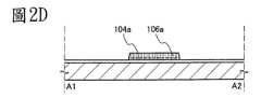
104:氧化物半導體層104: Oxide semiconductor layer
104a:氧化物半導體層104a: oxide semiconductor layer
104aa:非晶區104aa: amorphous region
104ab:結晶區104ab: crystallization area
105:氧化物半導體層105: Oxide semiconductor layer
106:氧化物半導體層106: Oxide semiconductor layer
106a:氧化物半導體層106a: oxide semiconductor layer
107a:導體層107a: Conductor layer
107b:導體層107b: Conductor layer
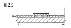
108:導體層108: Conductor layer
108a:源極或汲極電極層108a: Source or drain electrode layer
108b:源極或汲極電極層108b: Source or drain electrode layer
109a:絕緣層109a: Insulating layer
109b:絕緣層109b: Insulating layer
110:高純度結晶區110: High purity crystallization area
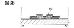
112:閘極絕緣層112: Gate insulation layer
114:閘極電極層114: Gate electrode layer
116:層間絕緣層116: Interlayer insulation layer
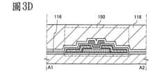
118:層間絕緣層118: Interlayer insulation layer
150:電晶體150: Transistor
200:基底200: Base
206:元件隔離絕緣層206: Component isolation insulation layer
208a:閘極絕緣層208a: Gate insulation layer
210a:閘極電極層210a: Gate electrode layer
214:雜質區214: Impurity zone
216:通道形成區216: Channel formation area
218:側壁絕緣層218: Side wall insulation layer
220:高濃度雜質區220: High concentration impurity area
224:金屬化合物區224: Metal compound area
226:層間絕緣層226: Interlayer insulation layer
228:層間絕緣層228: Interlayer insulation layer
230a:源極或汲極電極層230a: Source or drain electrode layer
230b:源極或汲極電極層230b: Source or drain electrode layer
230c:電極230c:Electrode
234:絕緣層234: Insulation layer
236a:電極236a:Electrode
236b:電極236b:Electrode
236c:電極236c:Electrode
250:電晶體250: Transistor
254a:電極254a:Electrode
254b:電極254b:Electrode
254c:電極254c:Electrode
254d:電極254d: Electrode
254e:電極254e:Electrode
256:絕緣層256: Insulation layer
258a:電極258a:Electrode
258b:電極258b:Electrode
258c:電極258c:Electrode
258d:電極258d:Electrode
301:主體301: Subject
302:機殼302: Chassis
303:顯示部303: Display unit
304:鍵盤304:Keyboard
311:主體311: Subject
312:探針312: Probe
313:顯示部313: Display unit
314:操作鍵314: Operation keys
315:外部介面315: External interface
320:電子書320: e-book
321:機殼321: Chassis
323:機殼323: Chassis
325:顯示部325: Display unit
327:顯示部327: Display unit
331:電源開關331: Power switch
333:操作鍵333: Operation key
335:揚音器335: Speaker
337:鉸鏈337: Hinge
340:機殼340: Chassis
341:機殼341: Chassis
342:顯示面板342: Display panel
343:揚音器343: Speaker
344:麥克風344: Microphone
345:操作鍵345: Operation keys
346:指向裝置346: Pointing device
347:相機鏡頭347: Camera lens
348:外部連接端子348: External connection terminal
349:太陽能電池349:Solar battery
350:外部記憶體插槽350: External memory slot
361:主體361: Subject
363:目鏡363: Eyepiece
364:操作開關364: Operation switch
365:顯示部365: Display Department
B367:顯示部B367: Display unit
A370:電視機A370:TV
371:機殼371: Chassis
373:顯示部373: Display unit
375:支架375: Bracket
377:顯示部377: Display unit
379:控制鍵379: Control key
380:遙控器380: Remote control
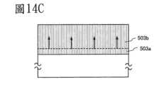
500:基部元件500: Base element
501:氧化物晶體層501: Oxide crystal layer
502:氧化物半導體層502: Oxide semiconductor layer
503a:氧化物晶體層503a: oxide crystal layer
503b:氧化物晶體層503b: oxide crystal layer
在附圖中:In the attached picture:
[圖1A及1B]是剖面視圖,顯示半導體裝置;[Figures 1A and 1B] are cross-sectional views showing a semiconductor device;
[圖2A至2E]是剖面視圖,顯示半導體裝置的製程;[Figures 2A to 2E] are cross-sectional views showing the manufacturing process of a semiconductor device;
[圖3A至3D]是剖面視圖,顯示半導體裝置的製程;[Figures 3A to 3D] are cross-sectional views showing the manufacturing process of a semiconductor device;
[圖4A至4C]是剖面視圖,顯示半導體裝置;[Figures 4A to 4C] are cross-sectional views showing semiconductor devices;
[圖5A至5C]是剖面視圖,顯示半導體裝置;[Figures 5A to 5C] are cross-sectional views showing semiconductor devices;
[圖6A及6B]是剖面視圖,顯示半導體裝置;[Figures 6A and 6B] are cross-sectional views showing a semiconductor device;
[圖7A及7B]是剖面視圖,顯示半導體裝置;[Figures 7A and 7B] are cross-sectional views showing a semiconductor device;
[圖8A至8D]是剖面視圖,顯示半導體裝置的製程;[Figures 8A to 8D] are cross-sectional views showing the manufacturing process of a semiconductor device;
[圖9A至9C]是剖面視圖,顯示半導體裝置的製程;[Figures 9A to 9C] are cross-sectional views showing the manufacturing process of a semiconductor device;
[圖10A至10C]是剖面視圖,顯示半導體裝置的製程;[Figures 10A to 10C] are cross-sectional views showing the manufacturing process of a semiconductor device;
[圖11A至11C]是剖面視圖,均顯示半導體裝置;[Figures 11A to 11C] are cross-sectional views, all showing semiconductor devices;
[圖12A至12C]是剖面視圖,均顯示半導體裝置;[Figures 12A to 12C] are cross-sectional views, all showing semiconductor devices;
[圖13]是剖面視圖,顯示半導體裝置;[Figure 13] is a cross-sectional view showing a semiconductor device;
[圖14A至14C]是剖面視圖,顯示本發明的實施例;[Figures 14A to 14C] are cross-sectional views showing embodiments of the present invention;
[圖15A]是剖面TEM照片,[圖15B]是其概要圖;[Figure 15A] is a cross-sectional TEM photo, and [Figure 15B] is its schematic diagram;
[圖16A]是第二熱處理後的剖面TEM照片,[圖16B]是其概要圖;[Figure 16A] is a cross-sectional TEM photograph after the second heat treatment, and [Figure 16B] is its schematic diagram;
[圖17A]是比較實施例的剖面TEM照片,[圖17B]是其概要圖;[Figure 17A] is a cross-sectional TEM photograph of a comparative embodiment, and [Figure 17B] is its schematic diagram;
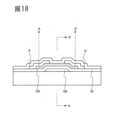
[圖18]是包含氧化物半導體的電晶體的剖面視圖;[Figure 18] is a cross-sectional view of a transistor including an oxide semiconductor;
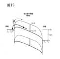
[圖19]是延著圖18中的A-A’的能帶圖(概要圖);[Figure 19] is the energy band diagram (summary diagram) along the A-A’ in Figure 18;
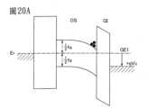
[圖20A]顯示正電位(+VG)施加至閘極(GE)的狀態,[圖20B]顯示負電位(-VG)施加至閘極(GE)的狀態;[FIG. 20A] shows a state where a positive potential (+VG ) is applied to the gate (GE), and [FIG. 20B] shows a state where a negative potential (-VG ) is applied to the gate (GE);
[圖21]顯示真空能階與金屬的功函數(ΦM)之間的關係及真空能階與氧化物半導體的電子親和力(χ)之間的關係。[Figure 21] shows the relationship between the vacuum energy level and the work function (ΦM ) of metals and the relationship between the vacuum energy level and the electron affinity (χ) of oxide semiconductors.
[圖22]顯示引起矽(Si)中熱載子注入之能量圖;[Figure 22] shows the energy diagram that causes hot carrier injection in silicon (Si);
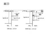
[圖23]顯示引起In-Ga-Zn-O為基礎的氧化物半導體(IGZO)中熱載子注入的能量圖;[Figure 23] shows the energy diagram that causes hot carrier injection in In-Ga-Zn-O based oxide semiconductor (IGZO);
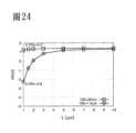
[圖24]顯示關於短通道效果的裝置模擬結果。[Figure 24] shows the device simulation results on the short channel effect.
[圖25]顯示關於短通道效果的裝置模擬結果。[Figure 25] shows the device simulation results regarding the short channel effect.
[圖26]顯示C-V(電容-電壓)特徵;[Figure 26] shows the C-V (capacitance-voltage) characteristics;
[圖27顯示Vg與(1/C)2之間的關係;[Figure 27 shows the relationship between Vg and (1/C)2 ;
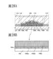
[圖28A及28B]是剖面視圖,顯示半導體裝置;[Figures 28A and 28B] are cross-sectional views showing a semiconductor device;
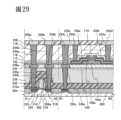
[圖29]是剖面視圖,顯示半導體裝置;及[Figure 29] is a cross-sectional view showing a semiconductor device; and
[圖30A至30F]顯示電子裝置。[Figures 30A to 30F] show electronic devices.
於下,將參考附圖,詳述本發明的實施例。注意,本發明不限於下述說明,以及,習於此技藝者清楚可知,在不悖離本發明的精神及範圍之下,可以以不同方式修改模式及細節。因此,本發明不應被解釋成侷限於下述實施例的說明。Below, the embodiments of the present invention will be described in detail with reference to the attached drawings. Note that the present invention is not limited to the following description, and it is clear to those skilled in the art that the modes and details can be modified in different ways without departing from the spirit and scope of the present invention. Therefore, the present invention should not be interpreted as being limited to the description of the following embodiments.
注意,為了便於瞭解,在某些情形中,圖式等中所示的每一結構的位置、尺寸、範圍、等等未準確地表示。因此,圖式等中揭示的本發明不侷限於這些位置、尺寸、範圍、等等。Note that for ease of understanding, in some cases, the position, size, range, etc. of each structure shown in the drawings, etc. are not accurately represented. Therefore, the present invention disclosed in the drawings, etc. is not limited to these positions, sizes, ranges, etc.
在本說明書中,使用例如「第一」及「第二」等序號以避免在元件之間造成混淆,這些名詞並非以數字方式限定元件。In this manual, serial numbers such as "first" and "second" are used to avoid confusion between components. These terms do not numerically limit the components.
在本實施例中,將參考圖1A及1B、圖2A至2E、圖3A至3D、及圖4A至4C,說明根據揭示的本發明的半導體裝置之結構及製造方法。In this embodiment, the structure and manufacturing method of the semiconductor device according to the present invention will be described with reference to FIGS. 1A and 1B, FIGS. 2A to 2E, FIGS. 3A to 3D, and FIGS. 4A to 4C.
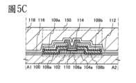
圖1A及1B是剖面視圖,顯示半導體裝置的結構實施例之電晶體150。注意,雖然此處所述的電晶體150是載子為電子的n通道IGFET(絕緣閘極場效電晶體),但是,電晶體150可以是p通道IGFET。1A and 1B are cross-sectional views showing a
電晶體150包含設於基底100上的第一氧化物半導體層104a上並以絕緣層102介於其間、設於第一氧化物半導體層104a上的第二氧化物半導體層106a、電連接至第二氧化物半導體層106a的源極或汲極電極層108a和源極或汲極電極層108b、遮蓋第二氧化物半導體層106a、源極或汲極電極層108a和源極或汲極電極層108b的閘極絕緣層112、以及在閘極絕緣層112上的閘極電極層114(請參見圖1A和1B)。The
此外,層間絕緣層116和層間絕緣層118設於電晶體150上。注意,層間絕緣層116和層間絕緣層118不是必要的元件,可以適當地省略。In addition,
關於第一氧化物半導體層104a和第二氧化物半導體層106a,可以使用四成分的金屬氧化物In-Sn-Ga-Zn-O為基礎的材料;三成分的金屬氧化物In-Ga-Zn-O為基礎的材料、In-Sn-Zn-O為基礎的材料、In-Al-Zn-O為基礎的材料、Sn-Ga-Zn-O為基礎的材料、Al-Ga-Zn-O為基礎的材料、或Sn-Al-Zn-O為基礎的材料;二成分的金屬氧化物In-Zn-O為基礎的材料、Sn-Zn-O為基礎的材料、Al-Zn-O為基礎的材料、Zn-Mg-O為基礎的材料、Sn-Mg-O為基礎的材料、或In-Mg-O為基礎的材料;或一成分金屬氧化物In-O為基礎的材料、Sn-O為基礎的材料、或Zn-O為基礎的材料;等等。For the first
此外,可以使用以In-A-B-O表示的氧化物半導體材料。此處,A代表選自例如鎵(Ga)或鋁(Al)等屬於13族的元素、以矽(Si)或鍺(Ge)為代表的屬於14族的元素、等等中之一或更多種元素。此外,B代表選自以鋅(Zn)為代表的屬於12族的元素之一或更多種元素。注意,自由地設定In含量、A含量、及B含量,以及,包含A含量為零的情形。另一方面,In含量及B含量不是零。換言之,上述表示包含In-Ga-Zn-O、In-Zn-O、等等。In addition, an oxide semiconductor material represented by In-A-B-O can be used. Here, A represents one or more elements selected from elements belonging to Group 13, such as gallium (Ga) or aluminum (Al), elements belonging to Group 14 represented by silicon (Si) or germanium (Ge), and the like. In addition, B represents one or more elements selected from elements belonging to Group 12 represented by zinc (Zn). Note that the In content, A content, and B content are freely set, and the case where the A content is zero is included. On the other hand, the In content and the B content are not zero. In other words, the above representation includes In-Ga-Zn-O, In-Zn-O, and the like.
特別地,當無電場且關閉狀態電流因而充份地降低時,In-Ga-Zn-O為基礎的氧化物半導體材料具有足夠高的電阻。此外,具有高的場效遷移率,In-Ga-Zn-O為基礎的氧化物半導體材料適用於半導體裝置中使用的半導體材料。In particular, the In-Ga-Zn-O-based oxide semiconductor material has a sufficiently high resistance when there is no electric field and the off-state current is thereby sufficiently reduced. In addition, having a high field effect mobility, the In-Ga-Zn-O-based oxide semiconductor material is suitable for semiconductor materials used in semiconductor devices.
關於In-Ga-Zn-O為基礎的氧化物半導體材料的典型實施例,以InGaO3(ZnO)m(m>0)表示。使用M取代Ga,會有以InMO3(ZnO)m(m>0)表示的氧化物半導體材料。此處,M代表選自鎵(Ga)、鋁(Al)、鐵(Fe)、鎳(Ni)、錳(Mn)、鈷(Co)、等等之一或更多金屬元素。舉例而言,M可為Ga、Ga及Al、Ga及Fe、Ga及Ni、Ga及Mn、Ga及Co、等等。注意,上述成分是從氧化物半導體材料具有的晶體結構導出且僅為實施例。A typical example of an oxide semiconductor material based on In-Ga-Zn-O is represented by InGaO3 (ZnO)m (m>0). When Ga is replaced by M, an oxide semiconductor material represented by InMO3 (ZnO)m (m>0) is obtained. Here, M represents one or more metal elements selected from gallium (Ga), aluminum (Al), iron (Fe), nickel (Ni), manganese (Mn), cobalt (Co), and the like. For example, M may be Ga, Ga and Al, Ga and Fe, Ga and Ni, Ga and Mn, Ga and Co, and the like. Note that the above components are derived from the crystal structure of the oxide semiconductor material and are merely examples.
較佳的是,以從第一氧化物半導體層104a和第二氧化物半導體層106a中充份地移除例如氫等雜質且將氧供應至其的方式,將第一氧化物半導體層104a和第二氧化物半導體層106a純化。具體而言,第一氧化物半導體層104a和第二氧化物半導體層106a中的氫濃度為5×10¹⁹/cm3或更低,較佳地為5×1018/cm3或更低,又更佳地為5×1017/cm3或更低。相較於具有約1×1014/cm3的載子密度之一般矽晶圓(添加有例如磷或硼等少量的雜質元素之矽晶圓),藉由充份地降低氫濃度及供應氧而被純化的第一氧化物半導體層104a和第二氧化物半導體層106a具有足夠低的載子密度(例如,小於1×1012/cm3,較佳地小於1.45×1010/cm3)。藉由使用i型的或實質上i型的氧化物半導體,取得具有極優良的關閉狀態電流特徵的電晶體150。舉例而言,當汲極電壓Vd是+1V或+10V及閘極電壓Vg從-20V至-5V時,關閉狀態電流為1×10-13A或更低。注意,以二次離子質譜儀(SIMS),則量第一氧化物半導體層104a和第二氧化物半導體層106a中的氫濃度。Preferably, the first
此處,較佳的是第一氧化物半導體層104a包含結晶區。結晶區較佳的是包含第一氧化物半導體104a的表面之區域,亦即,包含第一氧化物半導體層104a與第二氧化物半導體層106a之間的介面的區域,以及,較佳的是包含c軸在實質上垂直於第一氧化物半導體104a的表面之方向上對齊的晶體之區域。舉例而言,結晶區包含c軸在實質上垂直於第一氧化物半導體104a的表面之方向上對齊的晶粒。此處,「實質上垂直的方向」意指垂直方向±10°之內的方向。注意,結晶區僅形成於第一氧化物半導體層104a的表面近處中(例如,離表面2nm或更多且10nm或更少的距離(深度)之區域),或是形成為抵達第一氧化物半導體層104a的底部表面。Here, it is preferred that the first
此外,結晶區較佳地包含板狀晶體。此處,板狀晶體意指以平面方式且具有類似薄板的形狀之晶體。結晶區較佳地包含多晶體。In addition, the crystallization region preferably includes plate-like crystals. Here, the plate-like crystals refer to crystals that are in a planar manner and have a shape similar to a thin plate. The crystallization region preferably includes polycrystals.
第二氧化物半導體層106a包含從第一氧化物半導體層104a的結晶區的晶體生長所形成的晶體。The second
此處,由於第二氧化物半導體層106a包含從第一氧化物半導體層104a的結晶區的晶體生長所形成的晶體,所以,如同在第一氧化物半導體層104a的結晶區中一般,第二氧化物半導體層106a包含c軸在實質上垂直於第一氧化物半導體層104a與第二氧化物半導體層106a之間的介面的方向上對齊之第二氧化物半導體層106a。此處,「實質上垂直的方向」意指垂直方向±10°之內的方向。Here, since the second
此外,如同在第一氧化物半導體層104a的結晶區中一般,第二氧化物半導體層106a較佳地包含板狀晶體。第二氧化物半導體層106a較佳地包含多晶體。In addition, as in the crystallization region of the first
第二氧化物半導體層106a不僅包含從第一氧化物半導體層104a的晶體生長形成的晶體,也包含從第二氧化物半導體層106a的晶體生長形成的晶體。The second
在使用相同材料形成第一氧化物半導體層104a及第二氧化物半導體層106a的情形(亦即,在同質磊晶的情形)中,第一氧化物半導體層104a及第二氧化物半導體層106a之間的邊界可能無法分辨。雖然圖1A中邊界由點虛線顯示,但是,有第一氧化物半導體層104a及第二氧化物半導體層106a被視為一層的情形(請參見圖1A)。第一氧化物半導體層104a及第二氧化物半導體層106a都包含多晶體。In the case where the first
或者,第一氧化物半導體層104a及第二氧化物半導體層106a可由不同材料形成(請參見圖1B)。在第一氧化物半導體層104a及第二氧化物半導體層106a由不同材料形成的情形(亦即,在異質磊晶的情形)中,舉例而言,第一氧化物半導體層104a由二成分金屬氧化物的In-Zn-O為基礎的材料形成,以及,第二氧化物半導體層106a由三成分金屬氧化物的In-Ga-Zn-O為基礎的材料形成。Alternatively, the first
由於以第一氧化物半導體層104a的結晶區的晶體生長形成第二氧化物半導體層106a,所以,第二氧化物半導體層106a具有電各向異性。舉例而言,由於c軸在實質上垂直於第一氧化物半導體層104a與第二氧化物半導體層106a之間的介面的方向上對齊,所以,在與第二氧化物半導體層106a的表面平行的方向上的導電率增加。相對地,在與第二氧化物半導體層106a的表面垂直的方向上,絕緣特性增加。Since the second
在氧化物半導體層中作為通道形成區的區域至少具有平坦表面。第一氧化物半導體層及第二氧化物半導體層是多晶體,包含於第一氧化物半導體層及第二氧化物半導體層中的多晶體的c軸在相同方向上對齊。在與閘極電極層重疊的區域(通道形成區)中,第二氧化物半導體層的表面高度的變異較佳地為1nm或更少(又較佳地為0.2nm或更少)。The region serving as the channel formation region in the oxide semiconductor layer has at least a flat surface. The first oxide semiconductor layer and the second oxide semiconductor layer are polycrystalline, and the c-axes of the polycrystalline contained in the first oxide semiconductor layer and the second oxide semiconductor layer are aligned in the same direction. In the region overlapping with the gate electrode layer (channel formation region), the variation in the surface height of the second oxide semiconductor layer is preferably 1 nm or less (more preferably 0.2 nm or less).
如上所述,藉由使用由從經過純化的第一氧化物半導體層104a的結晶區的晶體生長形成的第二氧化物半導體層106a,可以實現具有有利的電特徵之半導體裝置。As described above, by using the second
第二氧化物半導體層106a是相當穩定的,因此,防止雜質(例如水)進入其中。因此,增進第二氧化物半導體層106a的可靠度。The second
於下,將說明氧化物半導體的純化造成氧化物半導體成為本質的(i型的)氧化物半導體的意義,在半導體裝置中使用此氧化物半導體的優點、等等。Below, we will explain the significance of purifying an oxide semiconductor to make it an intrinsic (i-type) oxide semiconductor, the advantages of using this oxide semiconductor in a semiconductor device, etc.
雖然已執行例如狀態密度(DOS)等氧化物半導體特性的研究,但是,它們未包含充份地降低缺陷程度本身的思想。根據揭示的本發明的實施例,藉由從氧化物半導體中移除可能造成DOS增加的水或氫,形成純化的本質(i型的)氧化物半導體。這是根據充份降低DOS本身的思想。因此,可以製造優良的產業產品。Although studies on oxide semiconductor properties such as density of states (DOS) have been conducted, they do not include the idea of sufficiently reducing the defect level itself. According to the disclosed embodiments of the present invention, a purified intrinsic (i-type) oxide semiconductor is formed by removing water or hydrogen that may cause an increase in DOS from the oxide semiconductor. This is based on the idea of sufficiently reducing DOS itself. Therefore, excellent industrial products can be manufactured.
注意,當移除氫、水、等等時,在某些情形中也移除氧。因此,有利的是藉由供應氧給因氧缺乏而產生的金屬的懸垂鍵並藉以降低導因於氧缺乏的DOS,而使氧化物半導體進一步被純化成為本質的(i型)氧化物半導體。舉例而言,以下述方式進一步降低導因於氧缺乏的DOS:形成與通道形成區緊密接觸的具有過量氧的氧化物膜;以及,執行高於或等於200℃且低於或等於400℃,典型上約250℃的熱處理,以致於氧從氧化物膜供應給氧化物半導體。在熱處理期間,氣體可以從惰性氣體切換成含氧的氣體。此外,接續在熱處理之後,藉由在充份地移除氫、水、等等的氛圍中或是氧氛圍中,執行溫度降低步驟,將氧供應至氧化物半導體。Note that when hydrogen, water, etc. are removed, oxygen is also removed in some cases. Therefore, it is advantageous to further purify the oxide semiconductor into an intrinsic (i-type) oxide semiconductor by supplying oxygen to the pendant bond of the metal generated by oxygen deficiency and thereby reducing the DOS due to oxygen deficiency. For example, the DOS due to oxygen deficiency is further reduced in the following manner: an oxide film having excess oxygen is formed in close contact with the channel formation region; and a heat treatment is performed at a temperature higher than or equal to 200°C and lower than or equal to 400°C, typically about 250°C, so that oxygen is supplied from the oxide film to the oxide semiconductor. During the heat treatment, the gas may be switched from an inert gas to a gas containing oxygen. Furthermore, oxygen is supplied to the oxide semiconductor by performing a temperature lowering step in an atmosphere in which hydrogen, water, etc. are sufficiently removed or in an oxygen atmosphere, following the heat treatment.
氧化物半導體特徵的劣化因素被視為是導因於在導電帶之下0.1eV至0.2eV的過量氫形成的淺能階、導因於氧缺乏的深能階、等等。Factors that deteriorate the characteristics of oxide semiconductors are considered to be shallow energy levels due to excess hydrogen formation 0.1eV to 0.2eV below the conduction band, deep energy levels due to oxygen deficiency, etc.
注意,雖然氧化物半導體通常具有n型導電率,所以,在所揭示的本發明之一實施例中,藉由移除例如水或氫等雜質及供應氧化物半導體的成份之氧而取得i型氧化物半導體。關於此點,由於與例如添加雜質元素的矽等i型半導體層不同,所以,可以說此處揭示的本發明的一實施例包含新穎的技術思想。Note that although oxide semiconductors generally have n-type conductivity, in one embodiment of the present invention disclosed, an i-type oxide semiconductor is obtained by removing impurities such as water or hydrogen and oxygen that supplies the components of the oxide semiconductor. In this regard, since it is different from an i-type semiconductor layer such as silicon to which an impurity element is added, it can be said that one embodiment of the present invention disclosed here includes a novel technical idea.
當使用i型氧化物半導體時,可以取得有利的電晶體溫度特徵。典型地,關於電晶體的電流-電壓特徵,在-25℃至150℃的溫度範圍中,開啟狀態電流、關閉狀態電流、場效遷移率、S值、及臨界電壓幾乎沒有變化,因此,電流-電壓特徵幾乎不會因溫度而劣化。When i-type oxide semiconductors are used, favorable transistor temperature characteristics can be obtained. Typically, regarding the current-voltage characteristics of the transistor, the on-state current, off-state current, field-effect mobility, S value, and critical voltage hardly change in the temperature range of -25°C to 150°C, so the current-voltage characteristics are hardly degraded by temperature.
使用本實施例中所述的氧化物半導體之電晶體具有比使用碳化矽的電晶體的遷移率低約二位數的遷移率。但是,藉由增加汲極電壓或通道寬度(W),使用氧化物半導體的電晶體的電流值增加;因此,增進裝置特徵。The transistor using the oxide semiconductor described in this embodiment has a mobility that is about two digits lower than that of the transistor using silicon carbide. However, by increasing the drain voltage or the channel width (W), the current value of the transistor using the oxide semiconductor increases; therefore, the device characteristics are improved.
本實施例的技術思想是藉由刻意地移除非所需地存在於氧化物半導體中的例如水或氫等雜質而未添加雜質至氧化物半導體,以純化氧化物半導體本身。換言之,本實施例的技術思想是藉由移除形成施子能階的水或氫並充份地供應氧化物半導體的主成分之氧以降低氧缺乏,來純化氧化物半導體。The technical idea of this embodiment is to purify the oxide semiconductor itself by intentionally removing impurities such as water or hydrogen that are not needed in the oxide semiconductor without adding impurities to the oxide semiconductor. In other words, the technical idea of this embodiment is to purify the oxide semiconductor by removing water or hydrogen that forms the donor energy level and fully supplying oxygen, the main component of the oxide semiconductor, to reduce oxygen deficiency.
根據SIMS(二次離子質譜儀)測量,正好在氧化物半導體沈積後,氫以約1×1020cm-3存在於氧化物半導體中。有意地移除造成施子能階的水或氫以及將因水或氫的移除而降低的氧(氧化物半導體的成分之一)添加至氧化物半導體,因而將氧化物半導體純化成電性上本質的(i型)半導體。According to SIMS (Secondary Ion Mass Spectrometry), hydrogen exists in the oxide semiconductor at about 1×1020 cm-3 just after the oxide semiconductor is deposited. Water or hydrogen causing the donor energy level is intentionally removed and oxygen (one of the components of the oxide semiconductor) reduced by the removal of water or hydrogen is added to the oxide semiconductor, thereby purifying the oxide semiconductor into an electrically intrinsic (i-type) semiconductor.
此外,在實施例中,較佳的是,水及氫的數量儘可能小,也是較佳的是,氧化物半導體中的載子數目僅可能小。換言之,需要小於1×1012cm-3,較佳地小於1.4×1010cm-3的載子密度,1.4×1010cm-3的載子密度是小於或等於測量極限。此外,在本實施例的技術思想中,理想的載子密度是0cm-3或是約0cm-3。特別地,當氧化物半導體在高於或等於450℃且低於或等於850℃,較佳地高於或等於550℃且低於或等於750℃下,在氧氛圍、氮氛圍、或超乾空氣氛圍(水含量小於或等於20ppm,較佳地小於或等於1ppm,更佳地小於或等於10ppb的空氣)中接受熱處理時,作為n型雜質的水或氫被移除且氧化物半導體被純化。此外,當藉由移除例如水或氫等雜質而純化氧化物半導體時,其載子密度可以小於1×1012cm-3,較佳地小於1.4×1010cm-3,1.4×1010cm-3是小於或等於測量極限。In addition, in the embodiment, it is preferred that the amount of water and hydrogen is as small as possible, and it is also preferred that the number of carriers in the oxide semiconductor is as small as possible. In other words, a carrier density of less than 1×1012 cm-3 , preferably less than 1.4×1010 cm-3 , is required, and a carrier density of 1.4×1010 cm-3 is less than or equal to the measurement limit. In addition, in the technical concept of the present embodiment, the ideal carrier density is 0 cm-3 or about 0 cm-3 . In particular, when the oxide semiconductor is subjected to heat treatment at a temperature higher than or equal to 450° C. and lower than or equal to 850° C., preferably higher than or equal to 550° C. and lower than or equal to 750° C., in an oxygen atmosphere, a nitrogen atmosphere, or an ultra-dry air atmosphere (air having a water content of less than or equal to 20 ppm, preferably less than or equal to 1 ppm, and more preferably less than or equal to10 ppb), water or hydrogen as n-type impurities is removed and the oxide semiconductor is purified. In addition, when the oxide semiconductor is purified by removing impurities such as water or hydrogen, its carrier density can be less than 1×1012 cm-3 , preferably less than 1.4×1010 cm-3, which is less than or equal to the measurement limit.
此外,當在高於或等於450℃且低於或等於850℃的溫度中,較佳地高於或等於600℃且低於或等於700℃的溫度中執行熱處理時,氧化物半導體純化,也結晶,晶體生長從氧化物半導體的表面朝向其內部進行,以致於氧化物半導體變成c軸對齊的多晶層。Furthermore, when heat treatment is performed at a temperature higher than or equal to 450°C and lower than or equal to 850°C, preferably higher than or equal to 600°C and lower than or equal to 700°C, the oxide semiconductor is purified and also crystallized, and crystal growth proceeds from the surface of the oxide semiconductor toward the inside thereof, so that the oxide semiconductor becomes a c-axis aligned polycrystalline layer.
根據本發明的實施例,使用c軸對齊的多晶層作為種晶,在其上形成第二氧化物半導體,以及,在高於或等於450℃且低於或等於850℃的溫度中,較佳地在高於或等於550℃且低於或等於750℃的溫度中,執行熱處理,以致於第二氧化物半導體變成c軸以類似於種晶的方式對齊的多晶層。也就是說,執行種晶的c軸與第二氧化物半導體的c軸在相同方向上對齊的理想軸向生長或磊晶生長。According to an embodiment of the present invention, a polycrystalline layer aligned in the c-axis is used as a seed crystal, a second oxide semiconductor is formed thereon, and heat treatment is performed at a temperature higher than or equal to 450°C and lower than or equal to 850°C, preferably at a temperature higher than or equal to 550°C and lower than or equal to 750°C, so that the second oxide semiconductor becomes a polycrystalline layer whose c-axis is aligned in a manner similar to the seed crystal. That is, ideal axial growth or epitaxial growth is performed in which the c-axis of the seed crystal is aligned in the same direction as the c-axis of the second oxide semiconductor.
不僅藉由沈積後的熱處理造成的固相生長,也藉由在高於或等於200℃且低於或等於600℃的溫度中受加熱的狀態下典型地以濺射沈積第二氧化物半導體的沈積期間之晶體生長,取得c軸以同於種晶的方向對齊之第二氧化物半導體。Not only by solid phase growth caused by heat treatment after deposition, but also by crystal growth during deposition of the second oxide semiconductor, typically by sputter deposition in a state heated at a temperature higher than or equal to 200°C and lower than or equal to 600°C, a second oxide semiconductor whose c-axis is aligned in the same direction as the seed crystal is obtained.
此外,氧化物半導體中的載子降低,或者,較佳地,所有載子被移除,以致於氧化物半導體作為電晶體中載子通過的路徑。結果,氧化物半導體是未具有載子或具有很少載子的純化的i型(本質的)半導體,以致於關閉狀態中電晶體的關閉狀態電流相當低,這是本實施例的技術思想。In addition, the carriers in the oxide semiconductor are reduced, or, preferably, all the carriers are removed, so that the oxide semiconductor serves as a path for the carriers in the transistor to pass through. As a result, the oxide semiconductor is a purified i-type (intrinsic) semiconductor having no carriers or very few carriers, so that the off-state current of the transistor in the off-state is quite low, which is the technical idea of the present embodiment.
此外,當氧化物半導體作為路徑以及氧化物半導體本身是未具有載子或具有很少載子的純化的i型(本質的)半導體時,由源極電極和汲極電極供應載子。當適當地選取電子親和力χ及費米能階,較佳地相當於氧化物半導體中的本質費米能階及源極電極和汲極電極的功函數之費米能階,載子可以從源極電極和汲極電極注入。因此,適當地製造n通道電晶體和p通道電晶體。Furthermore, when an oxide semiconductor serves as a path and the oxide semiconductor itself is a purified i-type (intrinsic) semiconductor having no carriers or few carriers, carriers are supplied by the source electrode and the drain electrode. When the electron affinity χ and the Fermi level are appropriately selected, preferably equivalent to the intrinsic Fermi level in the oxide semiconductor and the Fermi level of the work function of the source electrode and the drain electrode, carriers can be injected from the source electrode and the drain electrode. Therefore, n-channel transistors and p-channel transistors are appropriately manufactured.
在形成實質上平行於基底的通道之橫向式電晶體中,需要設置源極和汲極與通道,以致於增加基底中電晶體佔據的面積,這阻礙微小化。但是,在垂直式電晶體中,源極、通道、和汲極相堆疊,因而基底表面中由電晶體佔據的面積降低。由於此結果,能夠將薄膜電晶體微小化。In a lateral transistor that forms a channel substantially parallel to the substrate, it is necessary to set the source and drain together with the channel, so that the area occupied by the transistor in the substrate is increased, which hinders miniaturization. However, in a vertical transistor, the source, channel, and drain are stacked, so the area occupied by the transistor in the substrate surface is reduced. As a result, the thin film transistor can be miniaturized.
如上所述,氧化物半導體膜純化至含有儘可少的非氧化物半導體膜的主成分的雜質,典型上是氫、水、羥基、或氫化物,並使氧化物半導體膜包含多晶區,因而可以取得電晶體的有利操作。具體而言,耐受電壓增加,短通道效應降低,以及開/關比增加。此外,BT測試中電晶體的臨界電壓偏移量降低,以致於實現高可靠度。此外,電特徵的溫度相依性降低。在使用包含c軸對齊的多晶層之氧化物半導體層形成的電晶體中,在電晶體由光連續地照射的BT測試中,電晶體的臨界電壓偏移量降低。因此,製造具有穩定電特徵的電晶體。As described above, the oxide semiconductor film is purified to contain as few impurities as possible that are not the main components of the oxide semiconductor film, typically hydrogen, water, hydroxyl, or hydride, and the oxide semiconductor film is made to include a polycrystalline region, thereby enabling favorable operation of the transistor. Specifically, the withstand voltage is increased, the short channel effect is reduced, and the on/off ratio is increased. In addition, the critical voltage offset of the transistor in the BT test is reduced, so that high reliability is achieved. In addition, the temperature dependence of the electrical characteristics is reduced. In a transistor formed using an oxide semiconductor layer including a c-axis aligned polycrystalline layer, the critical voltage offset of the transistor is reduced in a BT test in which the transistor is continuously irradiated with light. Therefore, a transistor with stable electrical characteristics is manufactured.
關於與氧化物半導體相比之半導體材料,可為碳化矽(例如4H-SiC)等等。氧化物半導體與4H-SiC之間有一些共同性。載子濃度是氧化物半導體與4H-SiC之間的共同性之一實施例。根據費米-德瑞克(Fermi-Dirac),估算氧化物半導體的次要載子密度約為10-7/cm3。此次要載子密度值類似4H-SiC的次要載子密度,是極度小,4H-SiC的次要載子密度為6.7×10-11/cm3。當氧化物半導體的次要載子密度與矽的本質載子密度(約1.4×1010/cm3)相比時,可以良好地瞭解到氧化物半導體的次要載子密度顯著地低。Regarding semiconductor materials compared to oxide semiconductors, it can be silicon carbide (such as 4H-SiC) and the like. There are some commonalities between oxide semiconductors and 4H-SiC. Carrier concentration is one example of the commonality between oxide semiconductors and 4H-SiC. According to Fermi-Dirac, the secondary carrier density of oxide semiconductors is estimated to be about 10-7 /cm3 . This secondary carrier density value is similar to the secondary carrier density of 4H-SiC, which is extremely small. The secondary carrier density of 4H-SiC is 6.7×10⁻¹¹ /cm3 . When the secondary carrier density of oxide semiconductors is compared with the intrinsic carrier density of silicon (about 1.4×10¹⁰ /cm3 ), it can be well understood that the secondary carrier density of oxide semiconductors is significantly low.
此外,氧化物半導體的能帶隙大於或等於3.0eV且小於或等於3.5Ev,4H-SiC的能帶隙是3.26eV。因此,氧化物半導體與碳化矽類似地都是寬能帶隙半導體。In addition, the energy band gap of oxide semiconductors is greater than or equal to 3.0eV and less than or equal to 3.5Ev, and the energy band gap of 4H-SiC is 3.26eV. Therefore, oxide semiconductors are wide-bandgap semiconductors similar to silicon carbide.
另一方面,在氧化物半導體與碳化矽之間有主要的差異,亦即製程溫度。一般而言,當使用碳化矽時,要求高於或等於1500℃且低於或等於2000℃的熱處理。在此高溫下,使用碳化矽以外的材料之半導體基底、半導體元件、等等會損壞,因此,難以在使用碳化矽以外的半導體材料之半導體元件上形成使用碳化矽的半導體元件。另一方面,經由高於或等於300℃且低於或等於800℃的熱處理,可以取得氧化物半導體。因此,在形成使用其它半導體材料的積體電路之後,能夠形成使用氧化物半導體的半導體元件。On the other hand, there is a major difference between oxide semiconductors and silicon carbide, namely, the process temperature. Generally speaking, when using silicon carbide, heat treatment of 1500°C or higher and 2000°C or lower is required. At such high temperatures, semiconductor substrates, semiconductor elements, etc. using materials other than silicon carbide are damaged, and therefore, it is difficult to form semiconductor elements using silicon carbide on semiconductor elements using semiconductor materials other than silicon carbide. On the other hand, oxide semiconductors can be obtained by heat treatment of 300°C or higher and 800°C or lower. Therefore, semiconductor elements using oxide semiconductors can be formed after forming integrated circuits using other semiconductor materials.
在使用氧化物半導體的情形中,具有能夠使用具有低抗熱性的基底的優點,例如玻璃基底,不同於使用碳化矽的情形。此外,不用高溫處理,即能取得氧化物半導體,以致於相較於使用碳化矽的情形,能夠充份地降低能量成本。此外,在碳化矽中,晶體缺陷或是無意地被導入碳化矽中的小量雜質是產生載子的因素。理論上,在碳化矽的情形中,可以取得等於本發明的氧化物半導體的載子密度之低載子密度;但是,由於上述原因,所以,特別難以取得1012/cm3或更低的載子密度。當氧化物半導體與也是熟知的寬能帶隙半導體之氮化鎵相比時,同樣的情形也是為直。In the case of using an oxide semiconductor, there is an advantage that a substrate having low heat resistance, such as a glass substrate, can be used, unlike the case of using silicon carbide. In addition, the oxide semiconductor can be obtained without high-temperature treatment, so that the energy cost can be substantially reduced compared to the case of using silicon carbide. In addition, in silicon carbide, crystal defects or a small amount of impurities accidentally introduced into silicon carbide are factors that generate carriers. Theoretically, in the case of silicon carbide, a low carrier density equivalent to that of the oxide semiconductor of the present invention can be obtained; however, due to the above-mentioned reasons, it is particularly difficult to obtain a carrier density of 1012 /cm3 or less. The same is true when the oxide semiconductor is compared with gallium nitride, which is also a well-known wide-bandgap semiconductor.
將參考圖18、圖19A及圖19B、圖20A和20B、及圖21,說明包含氧化物半導體的電晶體的導電機制。注意,為了容易瞭解,下述說明是根據理想情形的假設,且未完全地反應真實的情形。此外,下述說明僅為一考量。The conduction mechanism of a transistor including an oxide semiconductor will be described with reference to FIG. 18 , FIG. 19A and FIG. 19B , FIG. 20A and FIG. 20B , and FIG. 21 . Note that for ease of understanding, the following description is based on the assumption of an ideal situation and does not fully reflect the actual situation. In addition, the following description is only a consideration.
圖18是包含氧化物半導體的電晶體(薄膜電晶體)的剖面視圖。氧化物半導體(OS)設於閘極電極(GE)上而以閘極絕緣層(GI)設於其間,以及,源極電極(S)和汲極電極(D)設於氧化物半導體層上。FIG18 is a cross-sectional view of a transistor (thin film transistor) including an oxide semiconductor. An oxide semiconductor (OS) is provided on a gate electrode (GE) with a gate insulating layer (GI) provided therebetween, and a source electrode (S) and a drain electrode (D) are provided on the oxide semiconductor layer.
圖19是圖18中的A-A’剖面之能帶圖(概要圖)。在圖19中,黑圓圈(●)及白圓圈(○)分別代表電子及電洞且分別具有電荷(-q,+q)。以正電壓(VD>0)施加至汲極電極,虛線顯示無電壓施加至閘極電極(VG=0)的情形,實線顯示正電壓施加至閘極電極(VG>0)的情形。在無電壓施加至閘極電極的情形中,由於高電位障壁,載子(電子)未從電極注入至氧化物半導體側,以致於沒有電流流通,意指關閉狀態。另一方面,當正電壓施加至閘極電極時,電位障壁降低,因此電流流通,意指開啟狀態。FIG19 is an energy band diagram (summary diagram) of the A-A' section in FIG18. In FIG19, black circles (●) and white circles (○) represent electrons and holes, respectively, and have charges (-q, +q), respectively. A positive voltage (VD >0) is applied to the drain electrode, the dotted line shows the case where no voltage is applied to the gate electrode (VG =0), and the solid line shows the case where a positive voltage is applied to the gate electrode (VG >0). In the case where no voltage is applied to the gate electrode, due to the high potential barrier, carriers (electrons) are not injected from the electrode to the oxide semiconductor side, so that no current flows, which means an off state. On the other hand, when a positive voltage is applied to the gate electrode, the potential barrier is lowered, so current flows, which means an on state.
圖20A及20B是圖18中的B-B’剖面之能帶圖(概要圖)。圖20A顯示正電壓(VG>0)施加至閘極電極(GE)的狀態及載子(電子)在源極電極與汲極電極之間流動的開啟狀態。圖20B顯示負電位(VG<0)施加至閘極電極(GE)的狀態及關閉狀態(次要載子未流動)。20A and 20B are energy band diagrams (synopsis) of the BB' section in FIG18. FIG20A shows a state where a positive voltage (VG >0) is applied to the gate electrode (GE) and an on state where carriers (electrons) flow between the source electrode and the drain electrode. FIG20B shows a state where a negative potential (VG <0) is applied to the gate electrode (GE) and an off state (secondary carriers do not flow).
圖21顯示真空位準與金屬的功函數(ΦM)之間的關係及氧化物半導體的真空能階與電子親和力(χ)之間的關係。FIG. 21 shows the relationship between the vacuum level and the work function (ΦM ) of metals and the relationship between the vacuum energy level and the electron affinity (χ) of oxide semiconductors.
由於在室溫度金屬中的電子衰退,所以費米能階位於導電帶。另一方面,習知的氧化物半導體是n型半導體,在該情形中,費米能階(EF)遠離位於能帶隙的中間之本質費米能階(Ei)並較接近導電帶。注意,知悉部份氫在氧化物半導體中作為施子且是造成氧化物半導體成為n型半導體的一因素。此外,知悉氧缺乏是產生n型氧化物半導體的原因之一。Since electrons in metals decay at room temperature, the Fermi level is located in the conduction band. On the other hand, a conventional oxide semiconductor is an n-type semiconductor, in which case the Fermi level (EF ) is far from the intrinsic Fermi level (Ei ) located in the middle of the energy band gap and is closer to the conduction band. Note that it is known that part of hydrogen acts as a donor in an oxide semiconductor and is a factor causing the oxide semiconductor to become an n-type semiconductor. In addition, it is known that oxygen deficiency is one of the causes of the generation of an n-type oxide semiconductor.
相對地,根據揭示的本發明的實施例之氧化物半導體是以下述方式成為本質的(i型)或是接近本質的氧化物半導體:從氧化物半導體移除產生n型氧化物半導體的起因之氫以便純化,以致於氧化物半導體的包含儘可能少的非氧化物半導體的主成分以外的元素(雜質元素),又移除氧缺乏。亦即,本發明的實施例的特點是未藉由添加雜質而是藉由移除儘可能多的氫和水等雜質及氧缺乏,而使氧化物半導體成為或接近純化的i型(本質的)半導體。因此,費米能階(EF)能夠與本質費米能階(Ei)是可相比的。In contrast, the oxide semiconductor according to the disclosed embodiment of the present invention becomes an intrinsic (i-type) or nearly intrinsic oxide semiconductor in the following manner: hydrogen, which is the cause of the generation of n-type oxide semiconductor, is removed from the oxide semiconductor for purification, so that the oxide semiconductor contains as few elements (impurity elements) other than the main component of the oxide semiconductor as possible, and oxygen deficiency is removed. That is, the embodiment of the present invention is characterized in that the oxide semiconductor becomes or nearly becomes a purified i-type (intrinsic) semiconductor by removing as many impurities such as hydrogen and water and oxygen deficiency as possible without adding impurities. Therefore, the Fermi level (EF ) can be comparable to the intrinsic Fermi level (Ei ).
可說氧化物半導體的能帶隙(Eg)是3.15Ev及電子親和力(χ)是4.3V。用於形成源極和汲極電極的鈦(Ti)的功函數實質上等於氧化物半導體的電子親和力(χ)。在該情形中,在金屬與氧化物半導體之間的介面處未形成電子的肖特基障壁。It can be said that the energy band gap (Eg ) of the oxide semiconductor is 3.15 Ev and the electron affinity (χ) is 4.3 V. The work function of titanium (Ti) used to form the source and drain electrodes is substantially equal to the electron affinity (χ) of the oxide semiconductor. In this case, a Schottky barrier of electrons is not formed at the interface between the metal and the oxide semiconductor.
在此時,如圖20A所示,電子在閘極絕緣層與純化的氧化物半導體之間的介面近處(氧化物半導體的底部部份,在能量上穩定的)中移動。At this time, as shown in FIG. 20A, electrons move in the vicinity of the interface between the gate insulating layer and the purified oxide semiconductor (the bottom part of the oxide semiconductor, which is energetically stable).
如圖20B所示,當負電位施加至閘極電極(GE)時,次要載子之電洞實質上未存在。因此,電流的值實質上接近零。As shown in FIG20B, when a negative potential is applied to the gate electrode (GE), the holes of the secondary carriers are substantially non-existent. Therefore, the value of the current is substantially close to zero.
以此方式,氧化物半導體藉由純化至含有儘可能少的其主成分以外的元素(雜質元素)而成為本質的(i型)或實質上本質的。因此,氧化物半導體與閘極絕緣層之間的介面的特徵變成顯著的。基於此理由,閘極絕緣層需要與氧化物半導體形成有利的介面。具體而言,較佳的是使用下述絕緣層,舉例而言:使用VHF頻帶至微波頻帶的範圍中的電源頻率產生的高密度電漿之CVD法形成的絕緣層、或是以濺射法形成的絕緣層。In this way, the oxide semiconductor becomes intrinsic (i-type) or substantially intrinsic by being purified to contain as few elements (impurity elements) other than its main component as possible. Therefore, the characteristics of the interface between the oxide semiconductor and the gate insulating layer become prominent. For this reason, the gate insulating layer needs to form a favorable interface with the oxide semiconductor. Specifically, it is preferable to use the following insulating layer, for example: an insulating layer formed by the CVD method using high-density plasma generated by a power frequency in the range of VHF band to microwave band, or an insulating layer formed by sputtering.
藉由純化氧化物半導體及形成氧化物半導體與閘極絕緣層之間的有利介面,舉例而言,當電晶體的通道寬度(W)是1×104μm以及其通道長度(L)為3μm時,取得關閉電流為10-13A或更低且次臨界擺幅值(S值)為0.1V/dec.(閘極絕緣膜的厚度:100nm)等特徵。By purifying the oxide semiconductor and forming a favorable interface between the oxide semiconductor and the gate insulating layer, for example, when the channel width (W) of the transistor is 1×104 μm and its channel length (L) is 3 μm, characteristics such as an off-current of 10-13 A or less and a subcritical swing amplitude (S value) of 0.1 V/dec. (thickness of the gate insulating film: 100 nm) are achieved.
當如上所述般純化氧化物半導體至含有儘可能少的其主元素以外之元素(雜質元素)時,電晶體可以以有利方式操作。When an oxide semiconductor is purified as described above to contain as few elements other than its main element (impurity elements) as possible, the transistor can operate in an advantageous manner.
接著,將參考圖22及圖23,說明使用氧化物半導體的電晶體之抗熱載子劣化。注意,為了容易瞭解,下述說明根據理想狀況的假設,且未完全反應真實情形。此外,下述說明僅為一考量。Next, the hot carrier degradation resistance of transistors using oxide semiconductors will be described with reference to Figures 22 and 23. Note that for ease of understanding, the following description is based on the assumption of ideal conditions and does not fully reflect the actual situation. In addition, the following description is only a consideration.
熱載子劣化的主要原因是通道熱電子注入(CHE注入)和汲極雪崩熱載子注入(DAHC注入)。注意,為了簡明起見,下述僅考慮電子。The main causes of hot carrier degradation are channel hot electron injection (CHE injection) and drain avalanche hot carrier injection (DAHC injection). Note that for simplicity, only electrons are considered below.
CHE注入意指一現象,其中,取得高於閘極絕緣層的障壁的能量之半導體層中的電子注入閘極絕緣層等等。電子藉由被低電場加速而取得能量。CHE injection refers to a phenomenon in which electrons in a semiconductor layer that have acquired energy higher than the barrier of a gate insulating layer are injected into a gate insulating layer, etc. The electrons acquire energy by being accelerated by a low electric field.
DAHC注入意指一現象,其中,被高電壓加速的電子之碰撞而產生的電子注入至閘極絕緣層等等。DAHC注入與CHE注入之間的差異是它們是否牽涉到因撞擊離子化造成的雪崩。注意,DAHC注入要求具有高於半導體的能帶隙之動能的電子。DAHC injection refers to a phenomenon in which electrons generated by collisions of electrons accelerated by high voltage are injected into a gate insulating layer, etc. The difference between DAHC injection and CHE injection is whether they involve avalanche due to impact ionization. Note that DAHC injection requires electrons with kinetic energy higher than the energy band gap of the semiconductor.
圖22顯示從矽(Si)的能帶結構估算之包含熱載子的注入之能量數量。圖23顯示包含熱載子注入的能量數量,其係從In-Ga-Zn-O為基礎的氧化物半導體(IGZO)的能帶結構估算而得的。在圖22及圖23中,在左側的圖顯示CHE注入及右側的圖顯示DAHC注入。FIG. 22 shows the amount of energy including hot carrier injection estimated from the band structure of silicon (Si). FIG. 23 shows the amount of energy including hot carrier injection estimated from the band structure of an In-Ga-Zn-O-based oxide semiconductor (IGZO). In FIG. 22 and FIG. 23, the left side graph shows CHE injection and the right side graph shows DAHC injection.
關於矽,由DAHC注入造成的劣化比CHE注入造成的劣化更嚴重。這導因於矽具有窄的能帶隙及雪崩容易於其中發生的事實。由於在矽中被加速而未碰撞的載子(例如,電子)是很少,所以,CHE注入的機率低。另一方面,雪崩增加能夠越過閘極絕緣層的障壁之電子數目,因此,DAHC注入的機率容易變成高於CHE注入的機率。Regarding silicon, the degradation caused by DAHC implantation is more severe than that caused by CHE implantation. This is due to the fact that silicon has a narrow energy band gap and avalanche easily occurs therein. Since there are few carriers (e.g., electrons) that are accelerated without colliding in silicon, the probability of CHE implantation is low. On the other hand, avalanche increases the number of electrons that can cross the barrier of the gate insulating layer, so the probability of DAHC implantation tends to become higher than that of CHE implantation.
關於In-Ga-Zn-O為基礎的氧化物半導體,包含CHE注入的能量數量與矽的情形並無大幅不同,而包含DAHC注入的能量數量實質上等於包含導因於寬能帶隙的CHE注入之能量數量。亦即,DAHC注入的機率低。For In-Ga-Zn-O based oxide semiconductors, the amount of energy involved in CHE implantation is not much different from that of silicon, and the amount of energy involved in DAHC implantation is substantially equal to the amount of energy involved in CHE implantation due to the wide energy bandgap. In other words, the probability of DAHC implantation is low.
以類似於矽的方式,被加速而未碰撞的載子(例如,電子)很少;因此,CHE注入的機率也低。亦即,In-Ga-Zn-O為基礎的氧化物半導體比矽具有更高的熱載子劣化抗性。In a manner similar to silicon, there are few carriers (e.g., electrons) that are accelerated without colliding; therefore, the probability of CHE injection is also low. That is, In-Ga-Zn-O-based oxide semiconductors have higher resistance to hot carrier degradation than silicon.
接著,將參考圖24,說明使用氧化物半導體的電晶體中的短通道效應。注意,為了容易瞭解,下述說明是根據理想情況的假設且未完全地反應真實的情形。此外,下述說明僅為一考慮。Next, the short channel effect in a transistor using an oxide semiconductor will be described with reference to FIG. 24. Note that for ease of understanding, the following description is based on the assumption of an ideal situation and does not fully reflect the actual situation. In addition, the following description is only a consideration.
短通道效應意指隨著電晶體的微小化(通道長度(L)縮減)變得顯著之電特徵劣化。短通道效應導因於源極上的汲極之效應。短通道效應的具體實施例是臨界電壓下降,次臨界擺幅(S值)增加、漏電流增加、等等。The short channel effect refers to the degradation of electrical characteristics that becomes significant as the transistor becomes smaller (the channel length (L) decreases). The short channel effect is caused by the effect of the drain on the source. Specific examples of the short channel effect are a decrease in critical voltage, an increase in subcritical swing (S value), an increase in leakage current, etc.
此處,以裝置模擬來檢查能夠抑制短通道效應的結構。具體而言,製備均具有不同的載子密度及不同厚度的氧化物半導體層之四種模型,以及,檢查通道長度(L)與臨界電壓(Vth)之間的關係。關於這些模型,使用均具有1.7×10⁻⁸/cm3或1.0×1015/cm3的載子密度及厚度1μm或30nm的氧化物半導體層之底部閘極型電晶體。注意,In-Ga-Zn-O為基礎的氧化物半導體用於氧化物半導體,以及,使用厚度100nm的氧氮化矽膜作為閘極絕緣層。Here, the structure capable of suppressing the short channel effect is examined by device simulation. Specifically, four models each having a different carrier density and a different thickness of an oxide semiconductor layer are prepared, and the relationship between the channel length (L) and the critical voltage (Vth ) is examined. For these models, bottom gate type transistors each having a carrier density of 1.7×10⁻⁸ /cm3 or 1.0×10¹⁵ /cm3 and an oxide semiconductor layer having a thickness of 1μm or 30nm are used. Note that an In-Ga-Zn-O-based oxide semiconductor is used for the oxide semiconductor, and a 100nm thick silicon oxynitride film is used as the gate insulating layer.
注意,在頂部閘極型電晶體與底部閘極型電晶體之間的計算結果中沒有顯著的差異。Note that there is no significant difference in the calculated results between the top-gate transistor and the bottom-gate transistor.
圖24及25顯示計算結果。圖24顯示載子密度為1.7×10⁻⁸/cm3的情形,圖25顯示載子密度為1.0×1015/cm3的情形。這些結果顯示藉由降低包含氧化物半導體的電晶體中的氧化物半導體層的厚度,可以抑制短通道效應。舉例而言,在通道長度幾乎為1μm的情形中,即使使用具有充份低的載子密度之氧化物半導體,仍然可以瞭解,當氧化物半導體層的厚度被設定為約3nm至50nm,較佳地約3nm至20nm,典型地約20nm時,短通道效應被充份地抑制。24 and 25 show the calculation results. FIG. 24 shows the case where the carrier density is 1.7×10⁻⁸ /cm3 , and FIG. 25 shows the case where the carrier density is 1.0×10¹⁵ /cm3. These results show that the short channel effect can be suppressed by reducing the thickness of the oxide semiconductor layer in the transistor including the oxide semiconductor. For example, in the case where the channel length is almost 1 μm, even if an oxide semiconductor with a sufficiently low carrier density is used, it can be understood that the short channel effect is sufficiently suppressed when the thickness of the oxide semiconductor layer is set to about 3 nm to 50 nm, preferably about 3 nm to 20 nm, and typically about 20 nm.
根據此處揭示的本發明之技術思想之一是藉由充份地降低氧化物半導體層的載子密度而將氧化物半導體層製成儘可能地接近本質(i型)氧化物半導體層。於下,將參考圖26及27,說明用於取得載子密度及氧化物半導體層中測量到的載子密度。One of the technical ideas of the present invention disclosed herein is to make the oxide semiconductor layer as close as possible to the intrinsic (i-type) oxide semiconductor layer by substantially reducing the carrier density of the oxide semiconductor layer. Below, the method for obtaining the carrier density and the carrier density measured in the oxide semiconductor layer will be described with reference to Figures 26 and 27.
以形成包含氧化物半導體層的MOS電容器以及估算MOS電容器的C-V測量(C-V特徵)之方式,取得氧化物半導體層中的載子密度。The carrier density in the oxide semiconductor layer is obtained by forming a MOS capacitor including the oxide semiconductor layer and estimating C-V measurement (C-V characteristics) of the MOS capacitor.
以下述步驟測量載子密度:步驟1,繪製閘極電壓Vg與MOS電容器的電容C之間的關係而取得C-V特徵曲線;步驟2,從C-V特徵取得代表閘極電壓Vg與(1/C)2之間的關係的圖形,以及,在圖中的弱反轉區中取得(1/C)2的微分值;以及,步驟3,將取得的微分值代入代表載子密度Nd的下述公式1。注意,在公式1中,e代表基本電荷,ε0代表真空介電常數,ε代表氧化物半導體的相對介電常數。The carrier density is measured by the following steps:

關於用於測量的樣品,使用具有下述結構的MOS電容器。MOS電容器包含在玻璃基底上300nm厚的鈦層、鈦層上100nm厚的氮化鈦層、在氮化鈦層上使用In-Ga-Zn-O為基礎的氧化物半導體(a-IGZO)之2μm厚的氧化物半導體層、在氧化物半導體層上300nm厚的氧氮化矽層、及在氧氮化矽層上300nm厚的銀層。As the sample used for measurement, a MOS capacitor having the following structure was used. The MOS capacitor includes a 300nm thick titanium layer on a glass substrate, a 100nm thick titanium nitride layer on the titanium layer, a 2μm thick oxide semiconductor layer using an In-Ga-Zn-O-based oxide semiconductor (a-IGZO) on the titanium nitride layer, a 300nm thick silicon oxynitride layer on the oxide semiconductor layer, and a 300nm thick silver layer on the silicon oxynitride layer.
使用用於沈積包含In、Ga、及Zn(In:Ga:Zn=1:1:0.5[原子%])的氧化物半導體之靶,以濺射法形成氧化物半導體層。形成氧化物半導體層的氛圍是氬及氧的混合氛圍(Ar及O2的流速分別為30(sccm)及15(sccm))。The oxide semiconductor layer was formed by sputtering using a target for depositing an oxide semiconductor containing In, Ga, and Zn (In:Ga:Zn=1:1:0.5 [atomic %]). The atmosphere for forming the oxide semiconductor layer was a mixed atmosphere of argon and oxygen (the flow rates of Ar and O2 were 30 (sccm) and 15 (sccm) respectively).
圖26顯示C-V特徵。圖27顯示Vg與(1/C)2之間的關係。從使用圖27中的弱反轉區中的(1/C)2的微分值之公式中取得的載子密度是6.0×1010/cm3。Fig. 26 shows the CV characteristics. Fig. 27 shows the relationship between Vg and (1/C)2. The carrier density obtained from the formula using the differential value of (1/C)2 in the weak inversion region in Fig. 27 is 6.0×10¹⁰ /cm3 .
藉由使用變成本質的或實質上本質的氧化物半導體(例如,載子密度小於1×10¹²/cm3及較佳地小於1.45×1010/cm3),可以取得具有優良的關閉狀態電流特徵的電晶體。By using an oxide semiconductor that becomes intrinsic or substantially intrinsic (e.g., having a carrier density less than 1×10¹² /cm3 and preferably less than 1.45×10¹⁰ /cm3 ), a transistor having excellent off-state current characteristics can be obtained.
如上所述,可知當使用氧化物半導體時,特別是純化的氧化物半導體時,可以取得各種有利的功效。此外,當如同揭示的本發明中所述般實現具有結晶結構的本質氧化物半導體層時,實現具有優良特徵的新穎半導體裝置。As described above, it can be seen that when an oxide semiconductor is used, especially a purified oxide semiconductor, various advantageous effects can be achieved. In addition, when an intrinsic oxide semiconductor layer having a crystalline structure is realized as described in the disclosed invention, a novel semiconductor device having excellent characteristics is realized.
接著,將參考圖2A至2E及圖3A至3D,說明電晶體150的製造方法。Next, the manufacturing method of
絕緣層102形成於基底100上。然後,第一氧化物半導體層形成於絕緣層102上,以及,執行第一熱處理以至少晶化包含第一氧化物半導體層的表面之區域,因而形成第一氧化物半導體層104(請參見圖2A)。An insulating
基底100可以是任何具有絕緣表面基底,以及,舉例而言,可為玻璃基底。由於能夠量產根據本發明的實施例之半導體裝置,所以,較佳的是使用玻璃基底。玻璃基底較佳的是非鹼性玻璃基底。關於非鹼性玻璃基底,舉例而言,使用例如矽酸鋁玻璃、硼矽酸鋁玻璃、硼矽酸鋇玻璃等玻璃材料。或者,關於基底100,使用由例如陶瓷基底、石英基底、或藍寶石基底等絕緣體形成的絕緣基底、使用例如矽等半導體材料形成且表面由絕緣材料遮蓋的半導體基底、或是由例如金屬或不銹鋼等導體形成且表面由絕緣材料遮蓋的導體基底。只要能夠承受製程中的熱處理,也可以使用塑膠基底。The
絕緣層102作為基部且由CVD法、濺射法、等等形成。絕緣層102較佳地形成為包含氧化矽、氮化矽、氧氮化矽、氮氧化矽、氧化鋁、氧化鉿、氧化鉭、等等。注意,絕緣層102可以具有單層結構或堆疊結構。對於絕緣層102的厚度並無特別限定;舉例而言,絕緣層102具有大於或等於10nm且小於或等於500nm的厚度。絕緣層102並非此處必要的元件;因此,未設置絕緣層102的結構也是可能的。The insulating
假使氫、水、等等含於絕緣層102中時,則氫進入氧化物半導體層或自氧化物半導體層取出氧,因而電晶體的特徵可能劣化。因此,希望形成絕緣層102為包含儘可能少的氫或水。If hydrogen, water, etc. are contained in the insulating
在使用濺射法等的情形中,舉例而言,希望在餘留於處理室中的濕氣被移除的狀態中,形成絕緣層102。為了移除餘留在處理室中的濕氣,較佳地使用吸附型真空泵,舉例而言,低溫泵、離子泵、或鈦昇華泵。使用設有冷阱的渦輪泵。在由低溫泵等抽真空的處理室中,充份地移除氫、水、等等;因此,可以降低絕緣層102中的雜質濃度。In the case of using a sputtering method, for example, it is desirable to form the insulating
當形成絕緣層102時,希望使用高純度氣體,其中,例如氫或水等雜質減少以致於濃度降低至約以「ppm」單位表示的值(較佳地,「ppb」)。When forming the insulating
使用四成分的金屬氧化物In-Sn-Ga-Zn-O為基礎的材料;三成分的金屬氧化物In-Ga-Zn-O為基礎的材料、In-Sn-Zn-O為基礎的材料、In-Al-Zn-O為基礎的材料、Sn-Ga-Zn-O為基礎的材料、Al-Ga-Zn-O為基礎的材料、或Sn-Al-Zn-O為基礎的材料;二成分的金屬氧化物In-Zn-O為基礎的材料、Sn-Zn-O為基礎的材料、Al-Zn-O為基礎的材料、Zn-Mg-O為基礎的材料、Sn-Mg-O為基礎的材料、或In-Mg-O為基礎的材料;或In-O為基礎的材料、Sn-O為基礎的材料、Zn-O為基礎的材料、等等。A material based on a four-component metal oxide In-Sn-Ga-Zn-O; a three-component metal oxide In-Ga-Zn-O based material, In-Sn-Zn-O based material, In-Al-Zn-O based material, Sn-Ga-Zn-O based material, Al-Ga-Zn-O based material, or Sn-Al-Zn-O based material; a two-component metal oxide In-Zn-O based material, Sn-Zn-O based material, Al-Zn-O based material, Zn-Mg-O based material, Sn-Mg-O based material, or In-Mg-O based material; or an In-O based material, a Sn-O based material, a Zn-O based material, and the like.
此外,可以使用以In-A-B-O表示的氧化物半導體材料。此處,A代表選自例如鎵(Ga)或鋁(Al)等屬於13族的元素、以矽(Si)或鍺(Ge)為代表的屬於14族的元素、等等中之一或更多種元素。此外,B代表選自以鋅(Zn)為代表的屬於12族的元素之一或更多種元素。注意,自由地設定In含量、A含量、及B含量,以及,包含A含量為零的情形。另一方面,In含量及B含量不是零。換言之,上述表示包含In-Ga-Zn-O、In-Zn-O、等等。In addition, an oxide semiconductor material represented by In-A-B-O can be used. Here, A represents one or more elements selected from elements belonging to Group 13 such as gallium (Ga) or aluminum (Al), elements belonging to Group 14 represented by silicon (Si) or germanium (Ge), and the like. In addition, B represents one or more elements selected from elements belonging to Group 12 represented by zinc(Zn). Note that the In content, A content, and B content are freely set, and the case where the A content is zero is included. On the other hand, the In content and the B content are not zero. In other words, the above representation includes In-Ga-Zn-O, In-Zn-O, and the like.
特別地,當無電場且關閉狀態電流因而充份地降低時,In-Ga-Zn-O為基礎的氧化物半導體材料具有足夠高的電阻。此外,具有高的場效遷移率,In-Ga-Zn-O為基礎的氧化物半導體材料適用於半導體裝置中使用的半導體材料。In particular, the In-Ga-Zn-O-based oxide semiconductor material has a sufficiently high resistance when there is no electric field and the off-state current is thereby sufficiently reduced. In addition, having a high field effect mobility, the In-Ga-Zn-O-based oxide semiconductor material is suitable for semiconductor materials used in semiconductor devices.
關於In-Ga-Zn-O為基礎的氧化物半導體材料的典型實施例,以InGaO3(ZnO)m(m>0)表示。使用M取代Ga,會有以InMO3(ZnO)m(m>0)表示的氧化物半導體材料。此處,M代表選自鎵(Ga)、鋁(Al)、鐵(Fe)、鎳(Ni)、錳(Mn)、鈷(Co)、等等之一或更多金屬元素。舉例而言,M可為Ga、Ga及Al、Ga及Fe、Ga及Ni、Ga及Mn、Ga及Co、等等。注意,上述成分是從氧化物半導體材料具有的晶體結構導出且僅為實施例。A typical example of an oxide semiconductor material based on In-Ga-Zn-O is represented by InGaO3 (ZnO)m (m>0). When Ga is replaced by M, an oxide semiconductor material represented by InMO3 (ZnO)m (m>0) is obtained. Here, M represents one or more metal elements selected from gallium (Ga), aluminum (Al), iron (Fe), nickel (Ni), manganese (Mn), cobalt (Co), and the like. For example, M may be Ga, Ga and Al, Ga and Fe, Ga and Ni, Ga and Mn, Ga and Co, and the like. Note that the above components are derived from the crystal structure of the oxide semiconductor material and are merely examples.
在本實施例中,使用用於沈積In-Ga-Zn-O為基礎的氧化物半導體之靶,以濺射法形成第一氧化物半導體。In this embodiment, a target for depositing an In-Ga-Zn-O-based oxide semiconductor is used to form a first oxide semiconductor by sputtering.
關於藉由濺射法用於沈積第一氧化物半導體層的靶,舉例而言,用於沈積包含In、Ga、及Zn的氧化物半導體之靶的成分比是使得In:Ga:Zn=1:x:y(x大於或等於0且小於或等於2,y大於或等於1且小於或等於5)。舉例而言,使用具有In:Ga:Zn=1:1:1[原子比](x=1,y=1)的成分比之靶(亦即,In2O3:Ga2O3:ZnO=1:1:1[莫耳比])。關於用於沈積氧化物半導體的靶,使用具有In:Ga:Zn=1:1:0.5[原子比]的成分比之靶、具有In:Ga:Zn=1:1:2[原子比]的成分比之靶、或是具有In:Ga:Zn=1:0:1[原子比]的成分比之靶。在本實施例中,為了稍後由熱處理造成刻意晶化,較佳地使用容易造成晶化之用於沈積氧化物半導體的靶。Regarding the target used for depositing the first oxide semiconductor layer by the sputtering method, for example, the composition ratio of the target used for depositing an oxide semiconductor containing In, Ga, and Zn is such that In:Ga:Zn=1:x:y (x is greater than or equal to 0 and less than or equal to 2, y is greater than or equal to 1 and less than or equal to 5). For example,a target having a composition ratio of In:Ga:Zn=1:1:1 [atomic ratio] (x=1, y=1) is used (that is, In2O3:Ga2O3:ZnO =1:1:1 [molar ratio]). As for the target for depositing the oxide semiconductor, a target having a composition ratio of In:Ga:Zn=1:1:0.5 [atomic ratio], a target having a composition ratio of In:Ga:Zn=1:1:2 [atomic ratio], or a target having a composition ratio of In:Ga:Zn=1:0:1 [atomic ratio] is used. In this embodiment, in order to cause intentional crystallization by heat treatment later, it is preferable to use a target for depositing the oxide semiconductor that is easy to crystallize.
此外,較佳的是含於用於沈積氧化物半導體的靶中含有的氧化物半導體具有80%或更高的相對密度,較佳地95%或更高,又更佳地99.9%或更高。藉由具有高的相對密度之用於沈積氧化物半導體的靶,第一氧化物半導體層形成為緻密的。在本實施例中,為了稍後由熱處理造成第一氧化物半導體層的刻意晶化,較佳的是使用能夠容易造成晶化之用於沈積氧化物半導體的靶。In addition, it is preferred that the oxide semiconductor contained in the target for depositing the oxide semiconductor has a relative density of 80% or more, preferably 95% or more, and more preferably 99.9% or more. By using the target for depositing the oxide semiconductor having a high relative density, the first oxide semiconductor layer is formed densely. In this embodiment, in order to cause the first oxide semiconductor layer to be intentionally crystallized by heat treatment later, it is preferred to use a target for depositing the oxide semiconductor that can easily cause crystallization.
形成第一氧化物半導體層的氛圍較佳地為稀有氣體(典型地,氬)氛圍、氧氛圍、或稀有氣體(典型地,氬)與氧的混合氛圍。具體而言,較佳的是使用例如氫、水、羥基、或氫化物等雜質被移除以致於濃度降低至約以「ppm」(較佳地,「ppb」)單位表示的值的高純度氣體氛圍。The atmosphere for forming the first oxide semiconductor layer is preferably a rare gas (typically, argon) atmosphere, an oxygen atmosphere, or a mixed atmosphere of a rare gas (typically, argon) and oxygen. Specifically, it is preferred to use a high-purity gas atmosphere in which impurities such as hydrogen, water, hydroxyl, or hydride are removed so that the concentration is reduced to a value expressed in about "ppm" (preferably, "ppb") units.
在形成氧化物半導體層時,舉例而言,基底被固持於維持在降壓的處理室中且基底溫度設定在等於或高於100℃且低於或等於600℃的溫度,較佳地高於或等於200℃且低於或等於400℃。然後,將氫及水被移除的濺射氣體導入餘留的濕氣已被移除的處理室中,使用金屬氧化物作為靶;如此,形成第一氧化物半導體層。當在加熱基底時形成氧化物半導體層時,能夠降低含於第一氧化物半導體層中的雜質。此外,降低濺射造成的損傷。較佳的是在第一氧化物半導體層形成之前、期間、或之後,移除餘留在濺射設備中的濕氣。為了移除餘留在處理室中的濕氣,較佳地使用吸附型真空泵。舉例而言,較佳地使用低溫泵、離子泵、鈦昇華泵、等等。或者,使用設有冷阱的渦輪泵。由於從由低溫泵抽真空的處理室中移除氫、水、等等,所以,降低第一氧化物半導體層中的雜質濃度。When forming the oxide semiconductor layer, for example, the substrate is held in a process chamber maintained at a reduced pressure and the substrate temperature is set at a temperature equal to or higher than 100°C and lower than or equal to 600°C, preferably higher than or equal to 200°C and lower than or equal to 400°C. Then, a sputtering gas from which hydrogen and water have been removed is introduced into the process chamber from which the remaining moisture has been removed, using a metal oxide as a target; thus, a first oxide semiconductor layer is formed. When the oxide semiconductor layer is formed while the substrate is heated, impurities contained in the first oxide semiconductor layer can be reduced. In addition, damage caused by sputtering is reduced. It is preferred to remove moisture remaining in the sputtering equipment before, during, or after the first oxide semiconductor layer is formed. In order to remove the moisture remaining in the processing chamber, an adsorption type vacuum pump is preferably used. For example, a cryogenic pump, an ion pump, a titanium sublimation pump, etc. are preferably used. Alternatively, a turbo pump provided with a cold trap is used. Since hydrogen, water, etc. are removed from the processing chamber evacuated by the cryogenic pump, the impurity concentration in the first oxide semiconductor layer is reduced.
舉例而言,第一氧化物半導體層的沈積條件如下所述:基底與靶之間的距離為170mm、壓力0.4Pa、直流(DC)電力為0.5kW、以及氛圍為氧氛圍(氧流量中氧的比例為100%)。注意,由於降低灰塵(膜沈積時產生的粉末或片狀物質以及使膜厚均勻,所以較佳地使用脈衝式直流(DC)電源。氧化物半導體層的厚度較佳地大於或等於3nm且小於或等於15nm,在本實施例中為5nm。注意,適當的厚度視氧化物半導體材料、用途、等等而不同,因此,可以視材料、用途、等等而適當地設定厚度。For example, the deposition conditions of the first oxide semiconductor layer are as follows: the distance between the substrate and the target is 170 mm, the pressure is 0.4 Pa, the DC power is 0.5 kW, and the atmosphere is an oxygen atmosphere (the proportion of oxygen in the oxygen flow is 100%). Note that a pulsed DC power supply is preferably used to reduce dust (powder or flake material generated during film deposition) and to make the film thickness uniform. The thickness of the oxide semiconductor layer is preferably greater than or equal to 3 nm and less than or equal to 15 nm, and is 5 nm in this embodiment. Note that the appropriate thickness varies depending on the oxide semiconductor material, application, etc., and therefore, the thickness can be appropriately set depending on the material, application, etc.
注意,在以濺射法形成第一氧化物半導體層之前,較佳地執行逆濺射,以致於移除附著於絕緣層102的表面的材料,在逆濺射中藉由導入的氬氣以及產生電漿。此處,逆濺射係一方法,其中,與使離子撞擊濺射靶之一般濺射相對地,使離子撞擊要處理的表面,以致於修改表面。使離子撞擊要處理的表面之方法的實施例是在氬氛圍中將高電源施加至表面,以致於在接近基底處產生電漿。注意,可以使用氮氛圍、氦氛圍、氧氛圍或類似者以取代氬氛圍。Note that before forming the first oxide semiconductor layer by sputtering, reverse sputtering is preferably performed so as to remove the material attached to the surface of the insulating
此外,在沈積第一氧化物半導體層之前,較佳地執行預熱處理,以移除移留在濺射設備的內壁上、靶表面上、或是靶材中的濕氣或氫。關於預熱處理,可以是在降壓下將沈積室的內部加熱至高於或等於200℃且低於或等於600℃的方法、膜沈積室的內部被加熱時重複導入及排出氮或惰性氣體之方法、等等。在預熱處理之後,將基底或濺射設備冷卻。然後,形成氧化物半導體層而未曝露至空氣。在此情形中,較佳地以油而非水或類似者作為用於靶的冷卻劑。雖然當重複導入及排出氮氣而未加熱時可以取得某種程度的效果,但是,又更佳的是以膜形成室的內部受加熱來執行處理。In addition, before depositing the first oxide semiconductor layer, it is preferable to perform a preheat treatment to remove moisture or hydrogen that has migrated on the inner wall of the sputtering equipment, on the target surface, or in the target material. Regarding the preheat treatment, it can be a method of heating the inside of the deposition chamber to a temperature higher than or equal to 200° C. and lower than or equal to 600° C. under reduced pressure, a method of repeatedly introducing and exhausting nitrogen or an inert gas while the inside of the film deposition chamber is heated, and the like. After the preheat treatment, the substrate or the sputtering equipment is cooled. Then, the oxide semiconductor layer is formed without being exposed to air. In this case, it is preferable to use oil rather than water or the like as a coolant for the target. Although a certain degree of effect can be achieved when nitrogen is repeatedly introduced and exhausted without heating, it is more preferable to perform the treatment with the interior of the film forming chamber heated.
接著,對第一氧化物半導體層執行第一熱處理以至少晶化包含第一氧化物半導體層的表面之區域,因而形成第一氧化物半導體層104。經由此第一熱處理,移除第一氧化物半導體層中的水(包含羥基)、氫、等等。第一熱處理的溫度高於或等於450℃且低於或等於850℃,較佳地高於或等於550℃且低於或等於750℃。加熱時間等於或大於1分鐘且小於或等於24小時。在本實施例中,在乾空氣氛圍中,在700℃下,執行熱處理一小時。Next, a first heat treatment is performed on the first oxide semiconductor layer to crystallize at least a region including the surface of the first oxide semiconductor layer, thereby forming the first
注意,在第一熱處理中,較佳的是氮、氧、或例如氦、氖、或氬等稀有氣體中未含有水、氫、等等。較佳的是,被導入至熱處理設備之氮、氧、或例如氦、氖、或氬等稀有氣體具有大於或等於6N(99.9999%)之純度,較佳地大於或等於7N(99.99999%)(亦即,雜質濃度設定為小於或等於1ppm,較佳地低於或等於0.1ppm)。在具有20ppm或更低濃度的H2O之超乾空氣中、更佳地在具有1ppm或更低濃度的H2O之超乾空氣中,執行第一熱處理。藉由此第一熱處理,移除第一氧化物半導體層104中的水(包含羥基)、氫、等等。因此,形成雜質降低之i型或實質上i型的第一氧化物半導體層104,使電晶體150能夠具有非常優良的特徵。Note that in the first heat treatment, it is preferred that nitrogen, oxygen, or a rare gas such as helium, neon, or argon contain no water, hydrogen, or the like. It is preferred that nitrogen, oxygen, or a rare gas such as helium, neon, or argon introduced into the heat treatment apparatus have a purity greater than or equal to 6N (99.9999%), preferably greater than or equal to 7N (99.99999%) (i.e., the impurity concentration is set to less than or equal to 1 ppm, preferably less than or equal to 0.1 ppm). The first heat treatment is performed in ultra-dry air having a H2 O concentration of 20 ppm or less, more preferably in ultra-dry air having a H2 O concentration of 1 ppm or less. Through the first heat treatment, water (including hydroxyl groups), hydrogen, etc. in the first
此外,當在第一熱處理中溫度增加時,加熱爐的內部可以設定在氮氛圍,以及,當執行冷卻時,加熱爐的內部切換至氧氛圍。藉由在氮氛圍中執行脫水或脫氫以及將氛圍切換至氧氛圍,氧供應至第一氧化物半導體層,以致於取得i型的氧化物半導體層。Furthermore, when the temperature is increased in the first heat treatment, the interior of the heating furnace may be set in a nitrogen atmosphere, and, when cooling is performed, the interior of the heating furnace is switched to an oxygen atmosphere. By performing dehydration or dehydrogenation in a nitrogen atmosphere and switching the atmosphere to an oxygen atmosphere, oxygen is supplied to the first oxide semiconductor layer, so that an i-type oxide semiconductor layer is obtained.
經由第一熱處理,形成在至少包含第一氧化物半導體層104的表面的區域中包含結晶區的第一氧化物半導體104。藉由從表面朝向內部的晶體生長,形成在包含表面的區域中形成的結晶區。結晶區包含c軸在實質上垂直於表面的方向上對齊的晶體。此處,「實質上垂直的方向」意指在垂直方向的±10°內。After the first heat treatment, a
雖然在本實施例中說明以第一熱處理晶化第一氧化物半導體層的整個區域的實施例,但是,只要在包含至少第一氧化物半導體層104的表面之區域中形成結晶區,本實質就不侷限於此。舉例而言,第一氧化物半導體層104在第一氧化物半導體層104的底表面近處中,亦即,在第一氧化物半導體層104與絕緣層102之間的介面,包含非晶區。因為防止結晶區中流動的載子被與絕緣層102之間的介面直接影響,所以,在第一氧化物半導體層104與絕緣層102之間的介面的近處中之非晶區的存在是有利的。Although the embodiment in which the entire region of the first oxide semiconductor layer is crystallized by the first heat treatment is described in this embodiment, the present invention is not limited thereto as long as a crystallized region is formed in a region including at least the surface of the first
注意,用於第一熱處理的設備並不限於特定的設備,可以使用來自例如電阻式加熱元件等加熱元件的熱傳導或熱輻射來加熱處理物品之設備。舉例而言,使用電熱爐、或例如氣體快速熱退火(GRTA)設備或燈快速熱退火(LRTA)設備等快速熱退火(RTA)設備。LRTA設備是使用來自例如鹵素燈、金屬鹵化物燈、氙電弧燈、碳電弧燈、高壓鈉燈、或高壓水銀燈等燈發射的光(電磁波)之輻射,將要處理的物體加熱。GRTA設備是使用高溫氣體之熱處理設備。Note that the equipment used for the first heat treatment is not limited to a specific equipment, and equipment that heats the treated article using heat conduction or heat radiation from a heating element such as a resistive heating element may be used. For example, an electric furnace or a rapid thermal annealing (RTA) equipment such as a gas rapid thermal annealing (GRTA) equipment or a lamp rapid thermal annealing (LRTA) equipment may be used. The LRTA equipment uses radiation from light (electromagnetic waves) emitted from lamps such as halogen lamps, metal halide lamps, xenon arc lamps, carbon arc lamps, high-pressure sodium lamps, or high-pressure mercury lamps to heat the object to be treated. The GRTA equipment is a heat treatment equipment that uses high-temperature gas.
接著,在包含至少表面的區域中包含結晶區的第一氧化物半導體層104上,形成第二氧化物半導體層105(請參見圖2B)。Next, a second
使用四成分的金屬氧化物In-Sn-Ga-Zn-O為基礎的材料;三成分的金屬氧化物In-Ga-Zn-O為基礎的材料、In-Sn-Zn-O為基礎的材料、In-Al-Zn-O為基礎的材料、Sn-Ga-Zn-O為基礎的材料、Al-Ga-Zn-O為基礎的材料、或Sn-Al-Zn-O為基礎的材料;二成分的金屬氧化物In-Zn-O為基礎的材料、Sn-Zn-O為基礎的材料、Al-Zn-O為基礎的材料、Zn-Mg-O為基礎的材料、Sn-Mg-O為基礎的材料、或In-Mg-O為基礎的材料;一成分金屬氧化物In-O為基礎的材料、Sn-O為基礎的材料、或Zn-O為基礎的材料;等等,以類似於第一氧化物半導體層的方式,形成第二氧化物半導體層105。A material based on a four-component metal oxide In-Sn-Ga-Zn-O; a three-component metal oxide In-Ga-Zn-O-based material, In-Sn-Zn-O-based material, In-Al-Zn-O-based material, Sn-Ga-Zn-O-based material, Al-Ga-Zn-O-based material, or Sn-Al-Zn-O-based material; a two-component metal oxide In-Zn -O-based materials, Sn-Zn-O-based materials, Al-Zn-O-based materials, Zn-Mg-O-based materials, Sn-Mg-O-based materials, or In-Mg-O-based materials; one-component metal oxide In-O-based materials, Sn-O-based materials, or Zn-O-based materials; etc., in a manner similar to the first oxide semiconductor layer, the second
特別地,當無電場且關閉狀態電流因而充份地降低時,In-Ga-Zn-O為基礎的氧化物半導體材料具有足夠高的電阻。此外,具有高的場效遷移率,In-Ga-Zn-O為基礎的氧化物半導體材料適用於半導體裝置中使用的半導體材料。In particular, the In-Ga-Zn-O-based oxide semiconductor material has a sufficiently high resistance when there is no electric field and the off-state current is thereby sufficiently reduced. In addition, having a high field effect mobility, the In-Ga-Zn-O-based oxide semiconductor material is suitable for semiconductor materials used in semiconductor devices.
關於In-Ga-Zn-O為基礎的氧化物半導體材料的典型實施例,以InGaO3(ZnO)m(m>0)表示。在上述結構中使用M取代Ga,有以InMO3(ZnO)m(m>0)表示的氧化物半導體材料。此處,M代表選自鎵(Ga)、鋁(Al)、鐵(Fe)、鎳(Ni)、錳(Mn)、鈷(Co)、等等之一或更多金屬元素。舉例而言,M可為Ga、Ga及Al、Ga及Fe、Ga及Ni、Ga及Mn、Ga及Co、等等。注意,上述成分是從氧化物半導體材料具有的晶體結構導出且僅為實施例。A typical example of an oxide semiconductor material based on In-Ga-Zn-O is represented by InGaO3 (ZnO)m (m>0). In the above structure, M is used instead of Ga, and there is an oxide semiconductor material represented by InMO3 (ZnO)m (m>0). Here, M represents one or more metal elements selected from gallium (Ga), aluminum (Al), iron (Fe), nickel (Ni), manganese (Mn), cobalt (Co), etc. For example, M can be Ga, Ga and Al, Ga and Fe, Ga and Ni, Ga and Mn, Ga and Co, etc. Note that the above composition is derived from the crystal structure of the oxide semiconductor material and is only an example.
較佳的是使用主成分與第一氧化物半導體層104的材料的主成分相同的材料以形成第二氧化物半導體層105,或者,第二氧化物半導體層105具有與第一氧化物半導體層104相同的晶體結構及類似於第一氧化物半導體層104(1%或更低的不匹配)的晶格常數。或者,使用具有不同主成分的材料,形成第一氧化物半導體層104及第二氧化物半導體層105。It is preferable to use a material having the same main component as the material of the first
在使用包含相同的主成分之材料的情形中,由於第一氧化物半導體層104的結晶區作為種晶,所以,在稍後的第二氧化物半導體層105的晶化中容易造成晶體生長。此外,由於厚度實質上增加,所以,使用包含相同主成分的材料適合應用於電力裝置等等。此外,在使用包含相同主成分的材料之情形中,可以取得例如黏著性等有利的介面特徵或是有利的電特徵。In the case of using materials containing the same main component, since the crystallization region of the first
在使用具有不同主成分的材料之情形中,這些層具有不同的電特徵。舉例而言,當具有高導電率的材料用於第二氧化物半導體層及具有低導電率的材料用於第一氧化物半導體層時,實現基部介面的影響降低之半導體裝置。在以容易晶化的材料用於第一氧化物半導體層以形成有利的種晶及接著形成和晶化第二氧化物半導體層的情形中,不論第二氧化物半導體層的晶化是否容易,第二氧化物半導體層都具有有利的結晶度。In the case of using materials with different main components, these layers have different electrical characteristics. For example, when a material with high conductivity is used for the second oxide semiconductor layer and a material with low conductivity is used for the first oxide semiconductor layer, a semiconductor device with reduced influence of the base interface is realized. In the case of using a material that is easy to crystallize for the first oxide semiconductor layer to form a favorable seed crystal and then forming and crystallizing the second oxide semiconductor layer, the second oxide semiconductor layer has a favorable crystallinity regardless of whether the second oxide semiconductor layer is easy to crystallize.
在本實施例中,使用用於沈積In-Ga-Zn-O為基礎的氧化物半導體之靶,以濺射法形成第二氧化物半導體層105。以類似於上述藉由濺射法沈積第一氧化物半導體層的方式,藉由濺射法,執行第二氧化物半導體層105的沈積。注意,第二氧化物半導體層105的厚度較佳地大於第一氧化物半導體層104的厚度。較佳地形成第二氧化物半導體層105,以致於第一氧化物半導體層104的厚度與第二氧化物半導體層105的厚度總合大於或等於3nm且小於或等於50nm。注意,適當的厚度視氧化物半導體的材料、用途、等等而變,因此,視氧化物半導體的材料、用途、等等,適當地選取厚度。In this embodiment, the second
接著,對第二氧化物半導體層105執行第二熱處理,以造成使用第一氧化物半導體層104的結晶區作為種晶之晶體生長。如此,形成第二氧化物半導體層106(請參見圖2C)。Next, a second heat treatment is performed on the second
第二熱處理的溫度高於或等於450℃且低於或等於850℃,較佳地高於或等於600℃且低於或等於700℃。第二熱處理的加熱時間大於或等於1小時且小於或等於100小時,較佳地大於或等於5小時且小於或等於20小時,典型地10小時。The temperature of the second heat treatment is higher than or equal to 450°C and lower than or equal to 850°C, preferably higher than or equal to 600°C and lower than or equal to 700°C. The heating time of the second heat treatment is greater than or equal to 1 hour and less than or equal to 100 hours, preferably greater than or equal to 5 hours and less than or equal to 20 hours, typically 10 hours.
注意,也在第二熱處理中,較佳的是氮、氧、或例如氦、氖、或氬等稀有氣體中未含有水、氫、等等。較佳的是,被導入至熱處理設備之氮、氧、或例如氦、氖、或氬等稀有氣體具有大於或等於6N(99.9999%)之純度,較佳地大於或等於7N(99.99999%)(亦即,雜質濃度設定為小於或等於1ppm,較佳地低於或等於0.1ppm)。在具有20ppm或更低濃度的H2O之超乾空氣中、更佳地在具有1ppm或更低濃度的H2O之超乾空氣中,執行第二熱處理。藉由此第二熱處理,移除第二氧化物半導體層106中的水(包含羥基)、氫、等等。因此,形成雜質降低之i型或實質上i型的第二氧化物半導體層106,使電晶體150能夠具有非常優良的特徵。Note that also in the second heat treatment, it is preferred that nitrogen, oxygen, or a rare gas such as helium, neon, or argon contain no water, hydrogen, or the like. It is preferred that nitrogen, oxygen, or a rare gas such as helium, neon, or argon introduced into the heat treatment apparatus have a purity greater than or equal to 6N (99.9999%), preferably greater than or equal to 7N (99.99999%) (i.e., the impurity concentration is set to less than or equal to 1 ppm, preferably less than or equal to 0.1 ppm). The second heat treatment is performed in ultra-dry air having a H2 O concentration of 20 ppm or less, more preferably in ultra-dry air having a H2 O concentration of 1 ppm or less. By this second heat treatment, water (including hydroxyl groups), hydrogen, etc. in the second
此外,當在第二熱處理中溫度增加時,加熱爐的內部可以設定在氮氛圍,以及,當執行冷卻時,加熱爐的內部切換至氧氛圍。藉由在氮氛圍中執行脫水或脫氫以及將氛圍切換至氧氛圍,氧供應至第二氧化物半導體層106,以致於取得i型的氧化物半導體層。In addition, when the temperature is increased in the second heat treatment, the interior of the heating furnace can be set in a nitrogen atmosphere, and, when cooling is performed, the interior of the heating furnace is switched to an oxygen atmosphere. By performing dehydration or dehydrogenation in a nitrogen atmosphere and switching the atmosphere to an oxygen atmosphere, oxygen is supplied to the second
依此方式,長時間地執行第二熱處理,第二氧化物半導體層105的整個區域從形成於第二氧化物半導體層105與第一氧化物半導體層104之間的介面近處中的結晶區結晶;因此,形成第二氧化物半導體層106。此外,藉由第二熱處理,第一氧化物半導體層104的結晶層具有更高的晶向。In this way, the second heat treatment is performed for a long time, and the entire region of the second
以類似於第一氧化物半導體層104的結晶區之方式,第二氧化物半導體層106包含c軸在實質上垂直於第一氧化物半導體層104與第二氧化物半導體層106之間的介面的方向上對齊的晶體。此處,「實質上垂直的方向」意指在垂直方向的±10°內。In a manner similar to the crystallization region of the first
舉例而言,在In-Ga-Zn-O為基礎的氧化物半導體材料用於第二氧化物半導體層106的情形中,第二氧化物半導體層106包含以InGaO3(ZnO)m(m>0,且m不是自然數)表示的晶體、以In2Ga2ZnO7(In:Ga:Zn:O=2:2:1:7)表示的晶體、等等。歸功於第二熱處理,此晶體的c軸在實質上垂直於氧化物半導體層106的表面之方向上對齊。For example, in the case where an In-Ga-Zn-O-based oxide semiconductor material is used for the second
此處,上述晶體包含In、Ga、及Zn中的任何元素,且被視為具有與a-軸及b-軸平行的複數層的堆疊結構。具體而言,上述晶體具有一結構,其中,包含In的層及未包含In的層(包含Ga或Zn的層)在c軸方向上堆疊。Here, the crystal contains any element of In, Ga, and Zn, and is considered to have a stacked structure of multiple layers parallel to the a-axis and the b-axis. Specifically, the crystal has a structure in which a layer containing In and a layer not containing In (a layer containing Ga or Zn) are stacked in the c-axis direction.
在In-Ga-Zn-O為基礎的氧化物半導體晶體中,在平行於a軸及b軸的方向上,包含In的層的導電率是有利的。這是因為導電率主要由In-Ga-Zn-O為基礎的氧化物半導體晶體中的In控制的事實以及一In原子的5s軌道與相鄰的In原子的5s軌道重疊,因而形成載子路徑。在垂直於上述層的方向上(亦即,c軸方向),增加絕緣特性。In an In-Ga-Zn-O-based oxide semiconductor crystal, the conductivity of the layer containing In is favorable in the direction parallel to the a-axis and the b-axis. This is due to the fact that the conductivity is mainly controlled by In in the In-Ga-Zn-O-based oxide semiconductor crystal and the 5s orbital of an In atom overlaps with the 5s orbital of an adjacent In atom, thereby forming a carrier path. In the direction perpendicular to the above layer (i.e., the c-axis direction), the insulating properties are increased.
在第一氧化物半導體層104在第一氧化物半導體層104與絕緣層102之間的介面近處中包含非晶區的情形中,第二熱處理造成從形成於第一氧化物半導體層104的表面上之結晶區朝向第一氧化物半導體層的底部表面之晶體生長,以及,在某些情形中使非晶區結晶。注意,視用於形成絕緣層102的材料或熱處理條件,非晶區可以維持。In the case where the first
在使用包含相同的主成分之氧化物半導體材料以形成第一氧化物半導體層104和第二氧化物半導體層105的情形中,如圖2C所示,晶體生長向上朝向第二氧化物半導體層105的表面,其中,第一氧化物半導體層104作為晶體生長的種晶,以致於形成第二氧化物半導體層106。第一氧化物半導體層104及第二氧化物半導體層106具有相同的晶體結構。因此,雖然第一氧化物半導體層104及第二氧化物半導體層106之間的邊界在圖2C中以虛線表示,但是,有時無法辨識,以及,第一氧化物半導體層104及第二氧化物半導體層106有時可以視為一層。In the case of using an oxide semiconductor material containing the same main component to form the first
由於藉由從第一氧化物半導體層104的結晶區之晶體生長來形成第二氧化物半導體層106,所以,第二氧化物半導體層106具有電性各向異性。在上述實施例中,在平行於第二氧化物半導體層106的表面之方向上,導電率增加,而在垂直於第二氧化物半導體層106的表面之方向上,絕緣特性增加。因此,使用藉由從純化的第一氧化物半導體層104的結晶層之晶體生長而形成的第二氧化物半導體層106,可以實現具有有利的電特徵之半導體裝置。Since the second
注意,用於第二熱處理的設備並不限於特定的設備,設備可以設有使用來自例如電阻式加熱元件等加熱元件的熱傳導或熱輻射來加熱處理物品之裝置。舉例而言,使用電熱爐、或例如GRTA設備或LRTA設備等RTA設備。Note that the equipment used for the second heat treatment is not limited to a specific equipment, and the equipment may be provided with a device for heating the treated article using heat conduction or heat radiation from a heating element such as a resistive heating element. For example, an electric heating furnace or an RTA equipment such as a GRTA equipment or an LRTA equipment is used.
接著,以例如使用掩罩的蝕刻等方法,處理第一氧化物半導體層104及第二氧化物半導體層106;因此,形成島狀第一氧化物半導體層104a和島狀第二氧化物半導體層106a。Next, the first
關於用於蝕刻氧化物半導體層的方法,可以使用乾蝕刻或濕蝕刻。無需多言,可以結合地使用乾蝕刻及濕蝕刻。視材料而適當地設定蝕刻條件(例如蝕刻氣體或蝕刻劑、蝕刻時間、及溫度),以致於氧化物半導體層被蝕刻成所需形狀。Regarding the method for etching the oxide semiconductor layer, dry etching or wet etching can be used. Needless to say, dry etching and wet etching can be used in combination. Etching conditions (such as etching gas or etchant, etching time, and temperature) are appropriately set depending on the material so that the oxide semiconductor layer is etched into a desired shape.
關於乾蝕刻法,可以使用平行板反應離子蝕刻(RIE)法、感應耦合電漿(ICP)蝕刻法、等等。也在此情形中,需要適當地設定蝕刻條件(例如,施加至線圈電極的電力量、施加至基底側上的電極之電力量、基底側上電極的溫度)。Regarding the dry etching method, parallel plate reactive ion etching (RIE) method, inductively coupled plasma (ICP) etching method, etc. can be used. In this case as well, it is necessary to appropriately set etching conditions (e.g., the amount of power applied to the coil electrode, the amount of power applied to the electrode on the substrate side, the temperature of the electrode on the substrate side).
用於乾蝕刻的蝕刻氣體之實施例是含氯的氣體(例如氯(Cl2)、三氯化硼(BCl3)、四氯化矽(SiCl4)、或四氯化碳(CCl4)等氯為基礎的氣體)。此外,可以使用含有氟的氣體(例如四氟化碳(CF4)、氟化硫(SF6)、三氟化氮(NF3)、或三氟甲烷(CHF3)等氟為基礎的氣體)、溴化氫(HBr)、氧(O2)、這些氣體中任何添加例如氦(He)或氬(Ar)等稀有氣體之氣體;等等。Examples of etching gases used for dry etching are chlorine-containing gases (e.g., chlorine (Cl2 ), boron trichloride (BCl3 ), silicon tetrachloride (SiCl4 ), or carbon tetrachloride (CCl4 ) and other chlorine-based gases). In addition, fluorine-containing gases (e.g., fluorine-based gases such as carbon tetrafluoride (CF4 ), sulfur fluoride (SF6 ), nitrogen trifluoride (NF3 ), or trifluoromethane (CHF3 )), hydrogen bromide (HBr), oxygen (O2 ), any of these gases to which a rare gas such as helium (He) or argon (Ar) is added, etc. may be used.
用於濕蝕刻的蝕刻劑之實施例包含磷酸、醋酸、及硝酸的混合溶液、過氧化銨混合物(含有31wt%的過氧化氫溶液:28wt%的氨溶液:水=5:2:2)、等等。也可以使用例如ITO-07N(KANTO CHEMICAL Co.,INC.的產品)等蝕刻劑。Examples of wet etching etchants include a mixed solution of phosphoric acid, acetic acid, and nitric acid, an ammonium peroxide mixture (containing 31wt% hydrogen peroxide solution: 28wt% ammonia solution: water = 5:2:2), etc. Etching agents such as ITO-07N (a product of KANTO CHEMICAL Co., INC.) can also be used.
接著,形成與第二氧化物半導體層106a接觸的導體層108(請參見圖2E)。Next, a
以例如濺射法等PVD法或例如電漿CVD法等CVD法,形成導體層108。使用選自鋁、鉻、銅、鉭、鈦、鉬、及鎢之元素、以及包含任何這些元素作為成份的合金、等等,形成導體層108。可以使用包含錳、鎂、鋯、及鈹之一或更多的材料。可以使用包含鋁與選自下述之一或更多元素的材料:鈦、鉭、鎢、鉬、鉻、釹、及鈧。
也可以使用導體金屬氧化物以形成導體層108。關於導體金屬氧化物,可以使用氧化銦(In2O3)、氧化錫(SnO2)、氧化鋅(ZnO)、氧化銦-氧化錫合金(In2O3-SnO2,在某些情形中縮寫為ITO)、氧化銦-氧化鋅合金(In2O3-ZnO)、或是包含矽或氧化矽的任何這些金屬氧化物材料。Conductive metal oxides may also be used to form the
關於導體層108,鋁層堆疊於鈦層上及鈦層堆疊於鋁層上的三層結構、或是鋁層堆疊於鉬層上及鉬層堆疊於鋁層上的三層結構是較佳的。或者,使用具有鋁層與鎢層堆疊的雙層結構、銅層與鎢層堆疊的雙層結構、或是鋁層與鉬層堆疊的雙層結構。無需多言,金屬導體層可以具有單層結構或是包含四或更多層的堆疊結構。在單層結構的情形中,舉例而言,有利地使用鈦層的單層結構。在使用具有單層結構的鈦層的情形中,藉由稍後要執行的蝕刻,取得有利的推拔狀。此處,使用包含鈦膜、鋁膜、及鈦膜的三層結構。Regarding the
在與第二氧化物半導體層106a接觸的部份導體層108中使用例如鈦等具有從第二氧化物半導體層106a中取出氧的能力之材料(具有高的氧親和力之材料)的情形中,與導體層108接觸的第二氧化物半導體層106a的區域因氧缺乏而變成具有n型導電率。利用此點,降低源極區和汲極區的電阻。In the case where a material such as titanium that has the ability to extract oxygen from the second
或者,不使用具有從第二氧化物半導體層106a中取出氧的能力之材料,而在第二氧化物半導體層106a與導體層108之間形成氧化物導體層。在設置此氧化物導體層的情形中,源極區和汲極區的電阻也降低。Alternatively, instead of using a material having the ability to extract oxygen from the second
此外,在與導體層108接觸的第二氧化物半導體層106a的區域不需變成具有n型導電率的情形中,在與第二氧化物半導體層106a接觸的導體層108的部份中,較佳地使用具有低的取出氧能加的材料(具有低的氧親和力之材料)。關於此材料,舉例而言,可為氮化鈦。以類似於上述的方式,導體層108可以具有單層結構或堆疊結構。在導體層108具有堆疊結構的情形中,舉例而言,使用氮化鈦膜及鈦膜的雙層結構、氮化鈦膜及鎢膜的雙層結構、氮化鈦膜及銅-鉬合金膜的雙層結構、氮化鉭膜及鎢膜的雙層結構、氮化鈦膜及銅膜的雙層結構、氮化鈦膜、鎢膜、及鈦膜的三層結構、等等。In addition, in the case where the region of the second
在上述具有低的取出氧的能力之材料用於導體層108的情形中,防止在氧化物半導體層因氧的取出而變成n型;因此,防止因不均勻的變成n型等造成電晶體特徵之不利影響。In the case where the above-mentioned material with low oxygen extraction ability is used for the
在如上所述使用例如氮化鈦膜或氮化鉭膜等具有高障壁特性的材料之情形中,在與第二氧化物半導體層106a接觸的導電層108的部份中,防止雜質進入第二氧化物半導體層106a以及降低對電晶體特徵的不利影響。In the case of using a material having high barrier properties such as a titanium nitride film or a tantalum nitride film as described above, in the portion of the
接著,選擇性地蝕刻導體層108以形成源極或汲極電極層108a和源極或汲極電極層108b(請參見圖3A)。此外,在導體層108上形成絕緣層,以及,將絕緣層蝕刻以在源極和汲極電極層上形成具有與源極或汲極電極層實質相同的形狀之絕緣層。在此情形中,降低源極和汲極電極層與閘極電極之間的電容(所謂的閘極電容)。注意,在本說明書中,「實質上相同的」說明無需嚴格地意指「完全地相同」且包含被視為相同的意義。舉例而言,由單一蝕刻處理產生的差異是可接受的。此外,厚度無需相同。Next, the
關於形成用於蝕刻的掩罩之曝光,較佳地使用紫外光、KrF雷射光、或ArF雷射光。特別是用於通道長度(L)小於25nm的情形之曝光,以具有極度短的數奈米至數十奈米的波長之極度紫外光,較佳地執行用於形成掩罩的曝光。在使用極度紫外光的曝光中,解析度高及聚焦深度大。因此,稍後完成的電晶體之通道長度(L)為10nm至1000nm(1μm)。藉由使用此方法而縮減通道長度,增進操作速度。此外,包含上述氧化物半導體的電晶體之關閉狀態電流小;因此,抑制導因於微小化的耗電增加。Regarding the exposure for forming a mask for etching, ultraviolet light, KrF laser light, or ArF laser light is preferably used. Especially for exposure in the case where the channel length (L) is less than 25nm, it is better to perform the exposure for forming the mask with extreme ultraviolet light having an extremely short wavelength of several nanometers to tens of nanometers. In the exposure using extreme ultraviolet light, the resolution is high and the depth of focus is large. Therefore, the channel length (L) of the transistor completed later is 10nm to 1000nm (1μm). By using this method, the channel length is shortened and the operating speed is increased. In addition, the off-state current of the transistor containing the above-mentioned oxide semiconductor is small; therefore, the increase in power consumption due to miniaturization is suppressed.
適當地調整導體層108及第二氧化物半導體層106a的材料及蝕刻條件,以致於在蝕刻導體層108時,第二氧化物半導體層106a不會被移除。注意,在某些情形中,第二氧化物半導體層106a在蝕刻步驟中被部份地移除並因而視材料及蝕刻條件而具有溝槽部(凹部)。The materials and etching conditions of the
在第一氧化物半導體層104a與第二氧化物半導體層106a的側表面的近處中,與源極或汲極電極層108a和源極或汲極電極層108b接觸的結晶層有改變成非晶狀態的情形。In the vicinity of the side surfaces of the first
為了降低使用的掩罩數目及步驟數目,藉由使用多色調掩罩形成的光阻掩罩,以執行蝕刻步驟,多色調掩罩是使光透射過而具有眾多強度的曝光掩罩。藉由使用多色調掩罩形成的光阻掩具有複數厚度(階梯狀),以及又可藉由執行灰化以改變形狀;因此,在眾多蝕刻步驟中使用光阻掩罩。亦即,藉由使用一個多色調掩罩,形成對應於至少二種不同圖案之光阻掩罩。因此,降低曝光掩罩的數目,也降低對應的微影步驟之數目,因而實現製程簡化。In order to reduce the number of masks and steps used, a photoresist mask formed by a multi-tone mask is used to perform the etching step. The multi-tone mask is an exposure mask with multiple intensities that allows light to pass through. The photoresist mask formed by using the multi-tone mask has multiple thicknesses (stepped) and can be changed in shape by performing ashing; therefore, the photoresist mask is used in many etching steps. That is, by using a multi-tone mask, a photoresist mask corresponding to at least two different patterns is formed. Therefore, the number of exposure masks is reduced, and the number of corresponding lithography steps is also reduced, thereby achieving process simplification.
此處,對第二氧化物半導體層106a執行熱處理(第三熱處理)。藉由第三熱處理,在包含第二氧化物半導體層106a的曝露表面及未與源極或汲極電極層108a也未與源極或汲極電極層108b重疊的第二氧化物半導體層106a的區域中形成高純度結晶區。此處,高純度結晶區是比第二氧化物半導體層106a中的其它區域具有更高的結晶度之區域。高純度結晶區的面積視第二氧化物半導體層106a的材料、熱處理條件、等等而變。舉例而言,高純度結晶區可以延伸至第二氧化物半導體層106a的下介面。Here, the second
關於第三熱處理,使用類似於第一熱處理的熱處理。換言之,採用使用電熱爐的熱處理、使用來自例如受熱氣體等媒介的熱傳導、使用熱輻射的熱處理、等等。Regarding the third heat treatment, a heat treatment similar to the first heat treatment is used. In other words, heat treatment using an electric furnace, heat conduction using a medium such as a heated gas, heat treatment using thermal radiation, etc. is adopted.
舉例而言,採用溫度高於或等於400℃且低於或等於900℃、使用高溫惰性氣體(例如,氮氣或稀有氣體)之GRTA處理。注意,雖然本發明的必要部份並未要特別的熱處理溫度上限,但是,在基底100具有低抗熱性的情形中,熱處理溫度的上限需要低於基底100的可允許溫度極限。For example, a GRTA treatment using a high-temperature inert gas (e.g., nitrogen or a rare gas) at a temperature higher than or equal to 400°C and lower than or equal to 900°C is used. Note that although the essential part of the present invention does not require a particular upper limit of the heat treatment temperature, in the case where the
在使用GRTA處理的情形中,熱處理的時間較佳地大於或等於1分別且小於或等於100分鐘。舉例而言,在650℃下,較佳地執行GRTA處理約3分鐘至6分鐘。藉由使用上述GRTA處理,可以在短時間內執行熱處理;因此,降低熱對於基底100的不利影響。亦即,相較於長時間執行熱處理的情形,在此情形中,增加熱處理溫度的上限。此外,在包含第二氧化物半導體層106a的表面之區域中,容易地形成高純度結晶區。In the case of using GRTA treatment, the time of heat treatment is preferably greater than or equal to 1 minute and less than or equal to 100 minutes respectively. For example, at 650°C, GRTA treatment is preferably performed for about 3 minutes to 6 minutes. By using the above-mentioned GRTA treatment, heat treatment can be performed in a short time; therefore, the adverse effect of heat on the
在第三熱處理中,較佳的是處理氛圍中未含有氫(包含水)等。舉例而言,被導入至熱處理設備之惰性氣體的純度是6N(99.9999%)或更高(亦即,雜質濃度為1ppm或更低),較佳地7N(99.99999%)或更高(亦即,雜質濃度為0.1ppm或更低)。取代惰性氣體,使用氫(包含水)被充份降低的氧氣、N2O氣體、超乾空氣(具有-40℃或更低的露點,較佳地-60℃或更低)。In the third heat treatment, it is preferred that the treatment atmosphere does not contain hydrogen (including water) or the like. For example, the purity of the inert gas introduced into the heat treatment equipment is 6N (99.9999%) or higher (i.e., the impurity concentration is 1 ppm or lower), preferably 7N (99.99999%) or higher (i.e., the impurity concentration is 0.1 ppm or lower). Instead of the inert gas, oxygen gas,N2O gas, or ultra-dry air (having a dew point of -40°C or lower, preferably -60°C or lower) in which hydrogen (including water) is sufficiently reduced is used.
雖然在本實施例中使用GRTA處理作為第三熱處理,但是,第三熱處理不侷限於GRTA處理。舉例而言,也可以採用使用電熱爐的熱處理、LRTA處理、等等。Although GRTA treatment is used as the third heat treatment in this embodiment, the third heat treatment is not limited to GRTA treatment. For example, heat treatment using an electric furnace, LRTA treatment, etc. may also be used.
以上述方式執行第三熱處理,造成再結晶以形成高純度結晶區,高純度結晶區是在包含晶體的第二氧化物半導體層106a中具有較高純度的結晶區。此外,在形成源極或汲極電極層108a及源極或汲極電極層108b時第二氧化物半導體層106a的表面受損之情形中,藉由第三熱處理,可以修復受損部份。The third heat treatment is performed in the above manner, causing recrystallization to form a high-purity crystallized region, which is a crystallized region having a higher purity in the second
以類似於上述晶體的方式,在以此方式形成的高純度結晶層中的氧化物半導體的晶體中,c軸在實質上垂直於氧化物半導體層的表面之方向上對齊。此處,「實質上垂直的方向」意指垂直方向±10°。In a manner similar to the above-mentioned crystal, in the crystal of the oxide semiconductor in the high-purity crystal layer formed in this manner, the c-axis is aligned in a direction substantially perpendicular to the surface of the oxide semiconductor layer. Here, "substantially perpendicular direction" means ±10° of the perpendicular direction.
藉由包含此高純度結晶區,第二氧化物半導體層106a具有更高的電性各向異性。By including this high-purity crystallized region, the second
藉由在第二氧化物半導體層106a中設置此高純度結晶層,可以增進半導體裝置的電特徵。By providing this high-purity crystal layer in the second
接著,形成與部份第二氧化物半導體層106a接觸而未曝露至空氣的閘極絕緣層112(請參見圖3B)。以CVD法、濺射法、等等形成閘極絕緣層112。閘極絕緣層112較佳地形成為包含氧化矽、氮化矽、氧氮化矽、氮氧化矽、氧化鋁、氧化鉿、氧化鉭、等等。注意,閘極絕緣層112可以具有單層結構或堆疊結構。對於閘極絕緣層112的厚度並無特別限定;舉例而言,閘極絕緣層112具有大於或等於10nm且小於或等於500nm的厚度,較佳地,大於或等於50nm且小於或等於200nm的厚度。Next, a
注意,藉由移除雜質而取得i型或實質上i型的氧化物半導體(純化的氧化物半導體)高度地受介面狀態或介面電荷影響;因此,閘極絕緣層112需要具有高品質。Note that obtaining an i-type or substantially i-type oxide semiconductor (purified oxide semiconductor) by removing impurities is highly affected by the interface state or interface charge; therefore, the
在本實施例中,使用高密度電漿設備,形成閘極絕緣層112。此處,高密度電漿設備意指能夠實現1×10¹¹/cm3或更高的電漿密度之設備。舉例而言,藉由施加高於或等於3kW且低於或等於6kW的微波功率以產生電漿,以致於形成絕緣膜。In this embodiment, a high-density plasma device is used to form the
舉例而言,由於能夠將閘極絕緣層形成為緻密的而具有高耐受電壓及高品質,所以,使用微波(例如2.45GHz)的高密度電漿CVD法是有利的。這是因為純化的氧化物半導體層與高品質閘極絕緣層之間的緊密接觸降低介面狀態密度及產生所需的介面特徵。For example, the high-density plasma CVD method using microwaves (e.g., 2.45 GHz) is advantageous because it can form a gate insulating layer densely with high withstand voltage and high quality. This is because the close contact between the purified oxide semiconductor layer and the high-quality gate insulating layer reduces the interface state density and produces the desired interface characteristics.
將單矽烷(SiH4)、氧化亞氮(N2O)、及稀有氣體作為源氣體導入腔室中,以在高於或等於10且低於或等於30Pa的壓力下產生高密度電漿,以致於形成閘極絕緣層112。之後,在停止單矽烷氣體(SiH4)的供應之後,將氧化亞氮(N2O)、及稀有氣體導入而不曝露至空氣中以致於對絕緣膜的表面執行電漿處理。至少在形成絕緣膜之後,執行藉由導入氧化亞氮(N2O)及稀有氣體而對絕緣膜的表面執行的電漿處理。經由上述處理程序而形成的絕緣膜具有小厚度且即使厚度小於例如100nm時仍然能夠確保可靠度。Monosilane (SiH4 ), nitrous oxide (N2 O), and a rare gas are introduced as source gases into the chamber to generate high-density plasma at a pressure greater than or equal to 10 and less than or equal to 30 Pa, so as to form the
在形成閘極絕緣膜112時,被導入腔室中的矽甲烷(SiH4)對氧化亞氮(N2O)的流量比在1:10至1:200的範圍中。此外,關於被導入腔室中的稀有氣體,使用氦、氬、氪、氙、等等。特別地,較佳地使用不昂貴的氬。When forming the
此外,由於使用高密度電漿設備形成的絕緣膜具有均勻厚度,所以,絕緣膜具有優良的步階遮蓋度。此外,藉由高密度電漿設備,可以精準地控制薄的絕緣膜的厚度。In addition, since the insulating film formed using high-density plasma equipment has a uniform thickness, the insulating film has excellent step coverage. In addition, the thickness of the thin insulating film can be precisely controlled by high-density plasma equipment.
經由上述製程程序形成的絕緣膜與使用傳統的平行板PCVD設備形成的絕緣膜大幅不同。在相互比較使用相同的蝕刻劑的蝕刻率的情形中,經由上述製程程序形成的絕緣膜的蝕刻率比使用傳統的平行板PCVD設備形成的絕緣膜的蝕刻率低10%或更多、或是低20%或更多。因此,可以說使用高密度電漿CVD設備形成的絕緣膜是緻密膜。The insulating film formed by the above process is significantly different from the insulating film formed using the conventional parallel plate PCVD equipment. When the etching rates using the same etchant are compared with each other, the etching rate of the insulating film formed by the above process is 10% or more lower, or 20% or more lower than the etching rate of the insulating film formed using the conventional parallel plate PCVD equipment. Therefore, it can be said that the insulating film formed using the high-density plasma CVD equipment is a dense film.
在本實施例中,使用由高密度電漿設備形成的厚度100nm的氧氮化矽膜(也稱為SiOXNy,其中,x>y>0)作為閘極絕緣層112。In this embodiment, a silicon oxynitride film (also referred to as SiOx Ny , where x>y>0) formed by a high-density plasma equipment with a thickness of 100 nm is used as the
無需多言,只要形成高品質絕緣層作為閘極絕緣層112,可以使用例如濺射法或電漿CVD法等其它方法。此外,能夠使用品質、介面特徵、等等藉由絕緣層形成後執行的熱處理增進的絕緣層。在任何情形中,形成具有降低介面狀態密度及形成與氧化物半導體層有利的介面之絕緣層、以及具有有利的膜品質以作為閘極絕緣層112。Needless to say, as long as a high-quality insulating layer is formed as the
藉由如此增進與閘極絕緣層112的介面之特徵及從氧化物半導體中消除雜質(特別是氫、水、等等),能夠取得臨界電壓(Vth)在閘極偏壓溫度測試(BT測試:例如,在85℃中及2×10⁶V/cm下12小時)中不會變化的穩定電晶體。By thus improving the characteristics of the interface with the
之後,在惰性氣體氛圍或氧氛圍中,較佳地執行第四熱處理。熱處理的溫度設定在200℃至400℃的範圍,較佳地,250℃至350℃。舉例而言,在氮氛圍中,在250℃下執行熱處理一小時。第四熱處理可以降低電晶體的電特徵變異。此外,也能夠藉由第四熱處理而供應氧給氧化物半導體層106a。Thereafter, a fourth heat treatment is preferably performed in an inert gas atmosphere or an oxygen atmosphere. The temperature of the heat treatment is set in the range of 200°C to 400°C, preferably 250°C to 350°C. For example, the heat treatment is performed at 250°C for one hour in a nitrogen atmosphere. The fourth heat treatment can reduce the electrical characteristic variation of the transistor. In addition, oxygen can also be supplied to the
注意,在本實施例中在形成閘極絕緣層112之後執行第四熱處理;只要是在第三熱處理之後執後,則對於第四熱處理的執行時機並無特別限定。此外,第四熱處理無需是必須的步驟。Note that in this embodiment, the fourth heat treatment is performed after the
接著,在與第一氧化物半導體層104a及第二氧化物半導體層106a重疊的區域中,在閘極絕緣層112上形成閘極電極層114(請參見圖3C)。在閘極絕緣層112上形成導體層,然後選擇性地圖型化導電層,以形成閘極電極層114。Next, a
以例如濺射法等PVD法或例如電漿CVD法等CVD法,形成上述導體層。使用選自鋁、鉻、銅、鉭、鈦、鉬、及鎢之元素、以及包含任何這些元素作為成份的合金、等等,形成導體層。或者,使用氮化鈦、氮化鉭、或上述元件的氮化物等。可以使用包含錳、鎂、鋯、及鈹之一或更多的材料。可以使用包含鋁與選自下述之一或更多元素的材料:鈦、鉭、鎢、鉬、鉻、釹、及鈧。The above-mentioned conductive layer is formed by a PVD method such as a sputtering method or a CVD method such as a plasma CVD method. The conductive layer is formed using an element selected from aluminum, chromium, copper, tungsten, titanium, molybdenum, and tungsten, and an alloy containing any of these elements as a component, etc. Alternatively, titanium nitride, tungsten nitride, or a nitride of the above-mentioned elements, etc. can be used. A material containing one or more of manganese, magnesium, zirconium, and curium can be used. A material containing aluminum and one or more elements selected from the following: titanium, tungsten, molybdenum, chromium, neodymium, and tungsten can be used.
也可以使用導體金屬氧化物以形成導體層。關於導體金屬氧化物,可以使用氧化銦(In2O3)、氧化錫(SnO2)、氧化鋅(ZnO)、氧化銦-氧化錫合金(In2O3-SnO2,在某些情形中縮寫為ITO)、氧化銦-氧化鋅合金(In2O3-ZnO)、或是包含矽或氧化矽的任何這些金屬氧化物材料。A conductive metal oxide may also be used to form the conductive layer. As the conductive metal oxide, indium oxide (In2O3 ), tin oxide (SnO2 ), zinc oxide (ZnO), indium oxide-tin oxide alloy (In2O3-SnO2, abbreviated as ITO in some cases), indium oxide-zinc oxide alloy (In2O3- ZnO), or any of these metal oxide materials containing silicon or silicon oxide may be used.
導體層可以具有單層結構或是二或更多層的堆疊結構。舉例言,可為包含矽的鋁膜之單層結構、鈦膜堆疊於鋁膜上的雙層結構、鈦膜堆疊於氮化鈦膜上的雙層結構、鎢膜堆疊於氮化鈦膜上的雙層結構、鎢膜堆疊於包含鉭和矽之氮化物膜上的雙層結構、鈦膜、鋁膜、及鈦膜堆疊的三層結構、等等。此處,使用包含鈦的材料以形成導體層,然後將導體層處理成閘極電極層114。The conductor layer may have a single-layer structure or a stacked structure of two or more layers. For example, it may be a single-layer structure of an aluminum film containing silicon, a double-layer structure of a titanium film stacked on an aluminum film, a double-layer structure of a titanium film stacked on a titanium nitride film, a double-layer structure of a tungsten film stacked on a titanium nitride film, a double-layer structure of a tungsten film stacked on a nitride film containing tungsten and silicon, a triple-layer structure of a titanium film, an aluminum film, and a titanium film stack, and the like. Here, a material containing titanium is used to form a conductor layer, and then the conductor layer is processed into a
接著,層間絕緣層116及層間絕緣層118形成於閘極絕緣層112和閘極電極層114之間(請參見圖3D)。以PVD法、CVD法、等等形成層間絕緣層116和118。使用包含例如氧化矽、氮氧化矽、氮化矽、氧化鉿、氧化鋁、或氧化鉭等無機絕緣材料的材料,形成層間絕緣層116和118。注意,在本實施例中層間絕緣層116和118堆疊,但是,所揭示的發明的實施例不限於本實施例。也可以使用單層結構或包含三或更多層的堆疊結構。Next, an
舉例而言,適當地以例如濺射法等不使例如水或氫等雜質進入於層間絕緣層118之方法,形成厚度至少1nm的層間絕緣層118。在本實施例中,以濺射法形成厚度300nm的氧化矽膜作為層間絕緣層118。在膜形成時的基底溫度可以高於或等於室溫且小於或等於300℃,在本實施例中為100℃。在稀有氣體(典型上,氬)氛圍中、氧氛圍中、或氧和稀有氣體(典型上,氬)氛圍中,以濺射法形成氧化矽膜。使用氧化矽靶或矽靶作為靶。舉例而言,在氧及氮的氛圍中,以濺射法沈積氧化矽。關於以具有降低的電阻設於氧化物半導體層上之層間絕緣層118,使用未包含例如濕氣、氫離子、或OH-等雜質且阻擋這些雜質從外部進入的無機絕緣膜。典型地,使用氧化矽膜、氮氧化矽膜、氧化鋁膜、氧氮化鋁膜、等等。此外,在層間絕緣層118上形成例如氮化矽膜或氮化鋁膜等保護絕緣層。For example, the
此外,在形成層間絕緣層118之前,較佳地執行預熱處理,以移除移留在濺射設備的內壁上、靶表面上、或是靶材中的水或氫。在預熱處理之後,將基底或濺射設備冷卻。然後,形成層間絕緣層118而未曝露至空氣。在此情形中,較佳地以油而非水或類似者作為用於靶的冷卻劑。雖然當重複導入及排出氮氣而未加熱時可以取得某種程度的效果,但是,又更佳的是以膜形成室的內部受加熱來執行處理。Furthermore, before forming the interlayer insulating
此外,在層間絕緣層118的膜形成之後,以濺射法在其上堆疊氮化矽膜,而不曝露至空氣。In addition, after the interlayer insulating
此外,在層間絕緣層118和層間絕緣層116中形成抵達閘極電極層114的接觸孔,以及在層間絕緣層118上形成電連接至閘極電極層114且供應閘極電位給閘極電極層114的連接電極。或者,可以使用下述:在形成層間絕緣層116之後形成抵達閘極電極層114的接觸孔;使用與源極電極層和汲極電極層相同的材料而在其上形成連接電極;層間絕緣層118形成於連接電極上;在層間絕緣層118中形成抵達連接電極的接觸孔;然後,在層間絕緣層118上形成電連接至連接電極且供應閘極電位給連接電極的電極。In addition, contact holes reaching the
注意,層間絕緣層118較佳地形成為具有平坦表面。這是因為當層間絕緣層118形成為具有平坦表面時在層間絕緣層118上有利地形成電極、佈線、等等。Note that the interlayer insulating
經由上述製程,完成包含由從第一氧化物半導體層104a的結晶層開始的晶體生長而形成的第二氧化物半導體層106a之電晶體150。Through the above process, the
歸功於包含在第二氧化物半導體層106a中的晶體,由上述方法製造的電晶體150具有有利的電特徵。Thanks to the crystal contained in the second
藉由第一熱處理及第二熱處理,執行結晶;藉由從氧化物半導體中移除n型雜質的氫而純化氧化物半導體,以致於儘可能地防止氧化物半導體的主成分以外的雜質含於其中。以此方式,形成本質的(i型)或實質上本質的氧化物半導體。換言之,未藉由添加雜質而是藉由儘可能地移除例如氫或水等雜質,取得純化的i型(本質的)半導體、或是接近i型(本質的)的半導體。藉由氧化物半導體層的純化,電晶體的臨界電壓變成正的,以致於取得所謂的常關電晶體150。Crystallization is performed by the first heat treatment and the second heat treatment; the oxide semiconductor is purified by removing hydrogen which is an n-type impurity from the oxide semiconductor, so that impurities other than the main component of the oxide semiconductor are prevented from being contained therein as much as possible. In this way, an intrinsic (i-type) or substantially intrinsic oxide semiconductor is formed. In other words, a purified i-type (intrinsic) semiconductor or a semiconductor close to i-type (intrinsic) is obtained without adding impurities but by removing impurities such as hydrogen or water as much as possible. By purifying the oxide semiconductor layer, the critical voltage of the transistor becomes positive, so that a so-called normally-
在以上述方法製造電晶體150的情形中,在第一氧化物半導體層104a和第二氧化物半導體層106a中的氫濃度小於或等於5×10¹⁸/cm3,以及電晶體150的關閉狀態電流小於或等於測量極限的1×10-13A。藉由使用因充份地降低氫濃度及氧供應而純化的第一氧化物半導體層104a和第二氧化物半導體層106a,電晶體150具有優良的特徵。In the case where the
一般而言傳統的氧化物半導體是n型的,即使閘極電壓是0V時,電流趨向在源極電極與汲極電極之間流動,亦即,電晶體趨向常開。即使當場效遷移率高時,假使電晶體常開時,難以控制電路。在氧化物半導體是n型的情形中,費米能階(Ef)較接近導電帶且遠離位於能帶隙的中間之本質費米能階(Ei)。知悉含於氧化物半導體中的部份氫形成施子且是造成氧化物半導體成為n型氧化物半導體的因素。Generally speaking, conventional oxide semiconductors are n-type, and even when the gate voltage is 0V, the current tends to flow between the source electrode and the drain electrode, that is, the transistor tends to be normally on. Even when the field effect mobility is high, it is difficult to control the circuit if the transistor is normally on. In the case where the oxide semiconductor is n-type, the Fermi level (Ef ) is closer to the conduction band and farther from the intrinsic Fermi level (Ei ) located in the middle of the energy band gap. It is known that part of the hydrogen contained in the oxide semiconductor forms a donor and is a factor that causes the oxide semiconductor to become an n-type oxide semiconductor.
慮及此點,以下述方式形成本質的(i型)或是實質上本質的氧化物半導體層:從氧化物半導體移除n型雜質的氫以便純化,以致於儘可能地防止氧化物半導體的主成分以外的雜質被包含於其中,來純化氧化物半導體。換言之,特點在於未藉由添加雜質而是藉由移除儘可能多的氫或水等雜質,形成純化的i型(本質的)半導體或是接近i型(本質的)的半導體。這使得費米能階(Ef)能夠與本質費米能階(Ei)在相同的位準。Taking this into consideration, an intrinsic (i-type) or substantially intrinsic oxide semiconductor layer is formed in the following manner: hydrogen which is an n-type impurity is removed from the oxide semiconductor for purification so as to prevent impurities other than the main component of the oxide semiconductor from being included therein as much as possible, thereby purifying the oxide semiconductor. In other words, the feature is that a purified i-type (intrinsic) semiconductor or a semiconductor close to i-type (intrinsic) is formed not by adding impurities but by removing as much impurities as possible such as hydrogen or water. This enables the Fermi level (Ef ) to be at the same level as the intrinsic Fermi level (Ei ).
藉由氧化物半導體層的純化,電晶體的臨界電壓是正的,因而實現所謂的常關切換元件。By purifying the oxide semiconductor layer, the critical voltage of the transistor is positive, thus achieving a so-called normally closed switching device.
關於純化製程,較佳的是在氧化物半導體層形成之前、期間、或之後,移除餘留在濺射設備中的濕氣等等。為了移除餘留在濺射室中的濕氣,較佳地使用吸附型真空泵。舉例而言,較佳地使用低溫泵、離子泵、鈦昇華泵、等等。使用設有冷阱的渦輪泵作為抽真空單元。由於從低溫泵抽真空的濺射設備的沈積室中移除氫原子、例如水(H2O)等含有氫原子的化合物,所以,降低形成於沈積室中的氧化物半導體膜中的雜質濃度。此外,較佳的是含於用於沈積的氧化物半導體靶中含有的氧化物半導體具有80%或更高的相對密度,較佳地95%或更高,又更佳地99.9%或更高。在使用具有高相對密度之靶的情形中,氧化物半導體膜中的雜質濃度降低。Regarding the purification process, it is preferable to remove moisture or the like remaining in the sputtering equipment before, during, or after the formation of the oxide semiconductor layer. In order to remove moisture remaining in the sputtering chamber, it is preferable to use an adsorption type vacuum pump. For example, it is preferable to use a cryogenic pump, an ion pump, a titanium sublimation pump, etc. A turbo pump provided with a cold trap is used as a vacuum pumping unit. Since hydrogen atoms, compounds containing hydrogen atoms such as water (H2O ) are removed from the deposition chamber of the sputtering equipment vacuumed by the cryogenic pump, the impurity concentration in the oxide semiconductor film formed in the deposition chamber is reduced. In addition, it is preferred that the oxide semiconductor contained in the oxide semiconductor target used for deposition has a relative density of 80% or more, preferably 95% or more, and more preferably 99.9% or more. In the case of using a target with a high relative density, the impurity concentration in the oxide semiconductor film is reduced.
假使雜質混入於氧化物半導體膜時,在稍後用於晶化的熱處理時,在一方向上的晶體生長,亦即,從表面向下進行的晶體生長中斷。因此,氧化物半導體膜未含有雜質是理想的。因此,純化是相當重要的。If impurities are mixed into the oxide semiconductor film, the crystal growth in one direction, that is, the crystal growth from the surface downward, is interrupted during the subsequent heat treatment for crystallization. Therefore, it is ideal that the oxide semiconductor film does not contain impurities. Therefore, purification is very important.
此外,在形成氧化物半導體膜之前,執行預熱處理,以移除移留在濺射設備的內壁上、靶表面上、或是靶材中的水或氫。關於預熱處理,可以是在降壓下將膜沈積室的內部加熱至從200℃至600℃的溫度之方法、膜沈積室的內部被加熱時重複導入及排出氮或惰性氣體之方法、等等。在此情形中,較佳地以油而非水或類似者作為用於靶的冷卻劑。雖然當重複導入及排出氮氣而未加熱時可以取得某種程度的效果,但是,更佳的是以膜形成室的內部受加熱來執行處理。在預熱處理之後,將基底或濺射設備冷卻,然後沈積氧化物半導體膜。In addition, before forming the oxide semiconductor film, a preheat treatment is performed to remove water or hydrogen that has migrated on the inner wall of the sputtering equipment, on the target surface, or in the target material. Regarding the preheat treatment, it can be a method of heating the inside of the film deposition chamber to a temperature of from 200°C to 600°C under reduced pressure, a method of repeatedly introducing and exhausting nitrogen or an inert gas while the inside of the film deposition chamber is heated, and the like. In this case, it is preferable to use oil rather than water or the like as a coolant for the target. Although a certain degree of effect can be achieved when nitrogen is repeatedly introduced and exhausted without heating, it is more preferable to perform the treatment with the inside of the film formation chamber heated. After the preheat treatment, the substrate or the sputtering equipment is cooled, and then the oxide semiconductor film is deposited.
也是關於用於沈積氧化物半導體膜或形成於氧化物半導體膜上且與其接觸的材料膜,較佳的是使用例如氫、水、羥基、或氫化物等雜質被移除以致於濃度降低至約以「ppm」(較佳地,「ppb」)單位表示的值的高純度氣體氛圍。Also related to a material film used for depositing an oxide semiconductor film or formed on and in contact with an oxide semiconductor film, preferably using a high purity gas atmosphere from which impurities such as hydrogen, water, hydroxyl, or hydride are removed so that the concentration is reduced to a value expressed in about "ppm" (preferably, "ppb") units.
在以濺射法形成氧化物半導體膜期間,基底被加熱至高於或等於室溫且低於或等於基底的應變點之溫度。During the formation of an oxide semiconductor film by sputtering, the substrate is heated to a temperature higher than or equal to room temperature and lower than or equal to the strain point of the substrate.
此外,關於純化的一步驟,在幾乎未含有氫及濕氣(例如氮氛圍、氧氛圍、或乾空氣氛圍(例如,對濕氣而言,露點為-40℃或更低,較佳地-50℃或更低)之氛圍中,執行第一熱處理。第一熱處理稱為脫水或脫氫,其中,從氧化物半導體層中消除H、OH、等等。在熱處理期間,在惰性氣體氛圍中升溫且氛圍切換至含有氧的氛圍之情形中,或者在使用氧氛圍的情形中,第一熱處理也可以稱為用於供應氧的處理。In addition, regarding the purification step, a first heat treatment is performed in an atmosphere containing almost no hydrogen and moisture (e.g., a nitrogen atmosphere, an oxygen atmosphere, or a dry air atmosphere (e.g., a dew point of -40°C or lower, preferably -50°C or lower for moisture). The first heat treatment is called dehydration or dehydrogenation, in which H, OH, etc. are eliminated from the oxide semiconductor layer. During the heat treatment, in the case where the temperature is increased in an inert gas atmosphere and the atmosphere is switched to an atmosphere containing oxygen, or in the case where an oxygen atmosphere is used, the first heat treatment can also be called a treatment for supplying oxygen.
關於第一熱處理,可以使用利用電熱爐的加熱方法、利用受熱氣體的氣體快速熱退火(GRTA)方法或利用燈光的燈快速熱退火(LRTA)方法、等等。此外,關於第一熱處理,同時執行使用波長小於或等於450nm的光來照射之加熱。在下述條件下,氧化物半導體層接受用於純化的第一熱處理:當以達到450℃之熱脫附沈積顯微法(TDS)測量第一熱處理後的氧化物半導體層時,不會偵測到水的二峰值中至少在約300℃的峰值。因此,即使對包含接受純化熱處理的氧化物半導體層之電晶體執行TDS至450℃的溫度,至少在約300℃的峰值不會被偵測到。Regarding the first heat treatment, a heating method using an electric furnace, a gas rapid thermal annealing (GRTA) method using a heated gas, or a lamp rapid thermal annealing (LRTA) method using a lamp, etc. can be used. In addition, regarding the first heat treatment, heating using light having a wavelength less than or equal to 450nm for irradiation is performed simultaneously. The oxide semiconductor layer is subjected to the first heat treatment for purification under the following conditions: when the oxide semiconductor layer after the first heat treatment is measured by thermal desorption deposition microscopy (TDS) at 450°C, at least one of the two peaks of water at about 300°C is not detected. Therefore, even if TDS is performed to a temperature of 450°C for a transistor including an oxide semiconductor layer subjected to the purification heat treatment, at least the peak at about 300°C is not detected.
由於在沒有作為晶體生長的多晶層之狀態下執行晶體生長,所以,較佳的是短時間地執行高溫下的第一熱處理,以僅從表面造成晶體生長。此外,當氧化物半導體層的表面是平坦時,取得有利的板狀多晶層。因此,較佳的是例如絕緣層或基底等基部元件的平坦度儘可能高。由於與基部元件的整個表面接觸的多晶層可以容易地形成,所以,平坦度增加是有效的。舉例而言,氧化物半導體層的平坦度幾乎等於商用矽晶圓的的平坦度;舉例而言,以AFM測量,在1μm×1μm的區域中高度的變異(表面粗糙度)小於或等於1nm,較佳地0.2nm。Since crystal growth is performed in a state where there is no polycrystalline layer grown as crystal, it is preferable to perform the first heat treatment at high temperature for a short time to cause crystal growth only from the surface. In addition, when the surface of the oxide semiconductor layer is flat, a favorable plate-shaped polycrystalline layer is obtained. Therefore, it is preferable that the flatness of the base element such as the insulating layer or the substrate is as high as possible. Since the polycrystalline layer in contact with the entire surface of the base element can be easily formed, the flatness increase is effective. For example, the flatness of the oxide semiconductor layer is almost equal to that of a commercial silicon wafer; for example, the variation in height (surface roughness) in an area of 1μm×1μm measured by AFM is less than or equal to 1nm, preferably 0.2nm.
在多晶層中,當包含於氧化物半導體中的In的電子雲彼此重疊且彼此連接時,導電率σ增加。因此,包含多晶層的電晶體具有高場效遷移率。In the polycrystalline layer, when the electron clouds of In contained in the oxide semiconductor overlap and connect to each other, the conductivity σ increases. Therefore, the transistor containing the polycrystalline layer has a high field effect mobility.
將參考圖14A至14C,說明使用經由第一熱處理形成的板狀多晶層作為種晶以造成晶體生長的一方法。A method of using a plate-shaped polycrystalline layer formed by a first heat treatment as a seed crystal to cause crystal growth will be described with reference to FIGS. 14A to 14C.
步驟次序的概要如下所述:在基部元件上形成第一氧化物半導體層;執行用於純化的第一熱處理;在與用於純化的第一熱處理相同的步驟中,在第一氧化物半導體層的表面上形成晶體方向對齊的多晶層;第二氧化物半導體層堆疊於其上;進一步地,執行用於晶化的第二熱處理,以致於藉由使用第一氧化物半導體層的表面上的多晶層作為種晶以晶化第二氧化物半導體層。The outline of the step sequence is as follows: forming a first oxide semiconductor layer on a base element; performing a first heat treatment for purification; forming a polycrystalline layer aligned in a crystal direction on a surface of the first oxide semiconductor layer in the same step as the first heat treatment for purification; stacking a second oxide semiconductor layer thereon; further, performing a second heat treatment for crystallization so that the second oxide semiconductor layer is crystallized by using the polycrystalline layer on the surface of the first oxide semiconductor layer as a seed crystal.
在第一熱處理中,在作為晶體生長的種晶之晶體層不存在的狀態中,從表面執行晶體生長;然而,在第二熱處理中,板狀多晶層作為種晶。因此,較佳的是,由於能夠取得有利的結晶度,所以,在能夠造成晶體生長的最低溫度下,長時間地執行第二熱處理。藉由第二熱處理的晶體生長方向對應於從下部朝上的方向,亦即,從基底側至表面側的方向(也稱為再結晶方向),且不同於藉由第一熱處理的晶體生長方向。此外,由於由第一熱處理取得的多晶層再度由第二熱處理加熱,所以,進一步地增加多晶層的結晶度。In the first heat treatment, crystal growth is performed from the surface in a state where a crystal layer serving as a seed crystal for crystal growth does not exist; however, in the second heat treatment, a plate-like polycrystalline layer serves as a seed crystal. Therefore, it is preferable to perform the second heat treatment for a long time at the lowest temperature that can cause crystal growth, since a favorable crystallinity can be obtained. The crystal growth direction by the second heat treatment corresponds to the direction from the bottom to the top, that is, the direction from the base side to the surface side (also called the recrystallization direction), and is different from the crystal growth direction by the first heat treatment. In addition, since the polycrystalline layer obtained by the first heat treatment is heated again by the second heat treatment, the crystallinity of the polycrystalline layer is further increased.
圖14A顯示對形成於基部元件500上的第一氧化物半導體層執行用於晶化的第一熱處理之後的狀態。FIG. 14A shows the state after the first heat treatment for crystallization is performed on the first oxide semiconductor layer formed on the
圖14B顯示正好在形成第二氧化物半導體層502之後時的剖面視圖。以濺射法形成第二氧化物半導體層502,以及,使用含有1:1:1[原子比]的In、Ga、及Zn的金屬氧化物靶或含有1:1:1[原子比]的In、Ga、及Zn的金屬氧化物靶作為此形成的金屬氧化物靶。FIG. 14B shows a cross-sectional view just after forming the second
圖14C是在第二熱處理後時的剖面視圖。藉由第二熱處理,使用第一氧化物半導體層的多晶層(第一氧化物晶體層501)作為種晶,晶體生長繼續向上進行至第二氧化物半導體層502的表面。結果,形成第二氧化物晶體層503。晶體元件具有相同的晶體結構。FIG. 14C is a cross-sectional view after the second heat treatment. By the second heat treatment, the polycrystalline layer (first oxide crystal layer 501) of the first oxide semiconductor layer is used as a seed crystal, and the crystal growth continues upward to the surface of the second
真正地製造相當於圖14B的結構。圖15A顯示結構的剖面之TEM照片。注意,其概要圖顯示於圖15B中。注意,使用高解析度透射式電子顯微鏡(Hitachi公司製造的「H9000-NAR」:TEM),以高倍率(八百萬倍放大率)及300Kv的加速電壓,拍攝TEM照片。以絕緣層形成於玻璃基底上、厚度5nm的第一In-Ga-Zn-O膜形成於其上、及在700℃下在乾空氣氛圍中對其執行熱處理一小時之方式,形成圖15A的樣品。從圖15A可以發現第一In-Ga-Zn-O膜的c軸在垂直於第一In-Ga-Zn-O膜的表面之方向上對齊,以及,絕緣層與第一In-Ga-Zn-O膜之間的介面的近處也結晶並具有在垂直於表面的方向上對齊的c軸。如圖14A所示,包含板狀多晶體的第一氧化物晶體層501形成於基部元件上。板狀多晶體較佳地為InGaZnO4(In:Ga:Zn:O=1:1:1:4)。此外,晶體的c軸方向對應於膜厚方向。A structure equivalent to FIG. 14B was actually manufactured. FIG. 15A shows a TEM photograph of a cross section of the structure. Note that its schematic diagram is shown in FIG. 15B. Note that the TEM photograph was taken using a high-resolution transmission electron microscope ("H9000-NAR" manufactured by Hitachi: TEM) at a high magnification (8 million times magnification) and an accelerating voltage of 300Kv. The sample of FIG. 15A was formed in such a manner that an insulating layer was formed on a glass substrate, a first In-Ga-Zn-O film with a thickness of 5nm was formed thereon, and a heat treatment was performed at 700°C in a dry air atmosphere for one hour. From FIG. 15A, it can be found that the c-axis of the first In-Ga-Zn-O film is aligned in a direction perpendicular to the surface of the first In-Ga-Zn-O film, and that the vicinity of the interface between the insulating layer and the first In-Ga-Zn-O film is also crystallized and has a c-axis aligned in a direction perpendicular to the surface. As shown in FIG. 14A, a first
在下述條件下,以使用用於沈積氧化物半導體的靶之濺射設備(用於沈積In-Ga-Zn-O為基礎的氧化物半導體(In2O3:Ga2O3:ZnO=1:1:2(莫耳比),In:Ga:Zn=1:1:1(原子比)),在下述條件下,沈積圖15A的樣品中的第一In-Ga-Zn-O膜:基底溫度為200℃且沈積速率為4nm/分鐘。不受限於靶的材料及成分,舉例而言,當使用含有1:1:1(莫耳比)的In2O3、Ga2O3、及ZnO之靶時,容易取得In2Ga2ZnO7的多晶體。The first In-Ga-Zn-O film in the sample of FIG. 15A was deposited under the following conditions using a sputtering apparatus (for depositing an In-Ga-Zn-O-based oxide semiconductor (In2 O3 :Ga2 O3 :ZnO=1:1:2 (molar ratio), In:Ga:Zn=1:1:1 (atomic ratio)) using a target for depositing an oxide semiconductor: substrate temperature was 200°C and deposition rate was 4 nm/min. Without being limited to the material and composition of the target, for example, when a target containing In2 O3 , Ga2 O3 , and ZnO at a molar ratio of 1:1:1 is used, polycrystals of In2 Ga2 ZnO7 are easily obtained.
In2Ga2ZnO7的晶體結構包含In、Ga、及Zn中任一者以及被視為具有平行於a-軸和b-軸的堆疊結構。由於In2Ga2ZnO7的晶體的導電率主要由In控制,所以,在平行於a-軸及b-軸的方向上含有In的層的電特徵是較佳的。在In2Ga2ZnO7的晶體中,In的電子雲彼此重疊且彼此連接,以致於形成載子路徑。The crystal structure of In2 Ga2 ZnO7 includes any one of In, Ga, and Zn and is considered to have a stacking structure parallel to the a-axis and b-axis. Since the conductivity of the crystal of In2 Ga2 ZnO7 is mainly controlled by In, the electrical characteristics of the layer containing In in the direction parallel to the a-axis and b-axis are better. In the crystal of In2 Ga2 ZnO7 , the electron clouds of In overlap and connect to each other, so as to form a carrier path.
取代上述靶,使用含有2:1:8(莫耳比)的In2O3、Ga2O3、及ZnO之金屬氧化物靶。Instead of the above target, a metal oxide target containing In2 O3 , Ga2 O3 , and ZnO in a molar ratio of 2:1:8 was used.
此外,可以使用含有1:2(莫耳比)的In2O3及ZnO但未包含Ga之金屬氧化物靶。假使形成底部閘極型電晶體時,由於Ga的氧化物是絕緣體,所以,相較於使用第一In-Ga-Zn-O膜的情形,藉由使用In-Zn-O膜,取得更高的場效遷移率。In addition, a metal oxide target containing In2 O3 and ZnO at a molar ratio of 1:2 but not including Ga can be used. If a bottom gate transistor is formed, since Ga oxide is an insulator, a higher field effect mobility can be obtained by using the In-Zn-O film compared to the case of using the first In-Ga-Zn-O film.
此外,由第一熱處理取得的多晶層再度由第二熱處理加熱而成為具有增進的結晶度之第三氧化物晶體層503a。In addition, the polycrystalline layer obtained by the first heat treatment is heated again by the second heat treatment to become a third
此外,可以說圖14C中所示的結構是雙層結構,其中,氧化物晶體層503a設於基部元件500上及與其接觸以及第二氧化物半導體層503b堆疊於其上。只要能夠取得c軸在垂直於表面的方向上對齊的多晶體,對於第一氧化物晶體層501及第二氧化物半導體層502的材料並無特別限定。第一氧化物晶體層501及第二氧化物半導體層502的材料可以不同或是含有相同的主成分。In addition, it can be said that the structure shown in FIG. 14C is a double-layer structure in which the
注意,在使用含有相同的主成分之氧化物半導體材料的情形中,如同圖14C中的虛線所示般,第三氧化物半導體層503a與第二氧化物晶體層503b之間的邊界不清楚,以致於第三氧化物半導體層503a及第二氧化物晶體層503b被視為一層。Note that in the case of using an oxide semiconductor material containing the same main component, as shown by the dotted line in FIG. 14C , the boundary between the third
以此方式,藉由二熱處理造成的晶體生長,取得第三氧化物晶體層503a和第二氧化物晶體層503b的堆疊形成的多晶層。In this way, through the crystal growth caused by the second heat treatment, a polycrystalline layer formed by the stacking of the third
注意,在圖14A中,晶體方向相對地對齊且形成於第一氧化物半導體層的表面部份中之多晶層的晶體生長從表面開始在膜厚方向上進行;因此,形成多晶層而不受基部元件影響。Note that in FIG. 14A, the crystal directions are relatively aligned and the crystal growth of the polycrystalline layer formed in the surface portion of the first oxide semiconductor layer proceeds from the surface in the film thickness direction; therefore, the polycrystalline layer is formed without being affected by the base element.
在第二In-Ga-Zn-O膜的沈積之後,以650℃,在氮氛圍中,執行熱處理6分鐘,以及取得剖面。圖16A是剖面的真實TEM照片。其概要圖顯示於圖16B中。在圖16A中,確認整個In-Ga-Zn-O膜結晶的狀態。此外,可以觀察到第二In-Ga-Zn-O膜的晶體具有在垂直於第二In-Ga-Zn-O膜的表面的方向上對齊的c軸。此外,可以發現即使在第二熱處理之後,絕緣層與第一In-Ga-Zn-O膜之間的介面的近處仍未結晶。After the deposition of the second In-Ga-Zn-O film, heat treatment was performed at 650°C in a nitrogen atmosphere for 6 minutes, and a cross section was obtained. FIG. 16A is a real TEM photograph of the cross section. Its schematic diagram is shown in FIG. 16B. In FIG. 16A, the state of crystallization of the entire In-Ga-Zn-O film is confirmed. In addition, it can be observed that the crystals of the second In-Ga-Zn-O film have a c-axis aligned in a direction perpendicular to the surface of the second In-Ga-Zn-O film. In addition, it can be found that even after the second heat treatment, the vicinity of the interface between the insulating layer and the first In-Ga-Zn-O film is still not crystallized.
將說明在例如In-Ga-Zn-O膜等第一氧化物半導體層的表面部份中形成晶體方向相對地對齊的晶體層之機制。藉由熱處理,包含於In-Ga-Zn-O膜中的鋅擴散且集中於表面的近處中,以及,變成晶體生長的種晶。在晶體生長中,晶體在橫向(平行於表面的方向)上比在深度方向上(垂直於表面的方向)生長得更多;因此,形成板狀多晶層。這些是從下述事實推定的:執行TDS測量達到450℃的溫度時,在真空熱條件下,特別是在約300℃,未偵測到In和Ga的峰值但是偵測到鋅的峰值之事實。注意,可以確認在真空中執行TDS測量以及在約200℃的溫度偵測到鋅。The mechanism of forming a crystal layer in which the crystal directions are relatively aligned in the surface portion of the first oxide semiconductor layer such as the In-Ga-Zn-O film will be explained. By heat treatment, zinc contained in the In-Ga-Zn-O film diffuses and concentrates in the vicinity of the surface, and becomes a seed crystal for crystal growth. In the crystal growth, the crystal grows more in the lateral direction (direction parallel to the surface) than in the depth direction (direction perpendicular to the surface); therefore, a plate-like polycrystalline layer is formed. This is inferred from the fact that when TDS measurement is performed up to a temperature of 450°C, under vacuum thermal conditions, particularly at about 300°C, peaks of In and Ga are not detected but a peak of zinc is detected. Note that it can be confirmed that TDS measurement is performed in a vacuum and zinc is detected at a temperature of about 200°C.
形成樣品作為比較實施例。以形成厚度50nm的In-Ga-Zn-O膜並使其接受700℃的加熱一小時之方式,形成樣品。圖17A顯示樣品的剖面之TEM照片。其概要圖顯示於圖17B中。注意,使用高解析度透射式電子顯微鏡(Hitachi公司製造的「H9000-NAR」:TEM),以高倍率(二百萬倍放大率)及300Kv的加速電壓,拍攝TEM照片。從圖17A可以發現從In-Ga-Zn-O膜的表面至約5nm的深度的區域結晶,以及,大量的非晶部份及晶向未對齊的眾多晶體任意地存在於In-Ga-Zn-O膜中。因此,可說即使當In-Ga-Zn-O膜沈積至例如50nm的大厚度並接著一次接受高於650℃的700℃熱處理一小時(這是大於6分鐘),則難以取得晶向整體地高度對齊之晶體層。A sample was formed as a comparative example. The sample was formed by forming an In-Ga-Zn-O film with a thickness of 50 nm and subjecting it to heating at 700°C for one hour. FIG. 17A shows a TEM photograph of a cross section of the sample. Its schematic diagram is shown in FIG. 17B. Note that the TEM photograph was taken using a high-resolution transmission electron microscope ("H9000-NAR": TEM manufactured by Hitachi Corporation) at a high magnification (2 million times magnification) and an accelerating voltage of 300Kv. From FIG. 17A, it can be found that there is regional crystallization from the surface of the In-Ga-Zn-O film to a depth of about 5 nm, and a large amount of amorphous parts and numerous crystals with misaligned crystal directions are randomly present in the In-Ga-Zn-O film. Therefore, it can be said that even when the In-Ga-Zn-O film is deposited to a large thickness of, for example, 50 nm and then subjected to a heat treatment of 700°C, which is higher than 650°C, for one hour (which is more than 6 minutes), it is difficult to obtain a crystal layer with highly aligned crystal directions as a whole.
從這些結果可以說以下述二沈積之方式形成具有大厚度的多晶層:形成作為晶體生長的種晶之多晶層,然後,沈積膜,然後執行晶體生長。因此,發現本說明書中揭示的方法極度有用。藉由執行沈積二次及執行熱處理二次,取得晶體方向高度對齊的結晶層,亦即,c軸在垂直於氧化物半導體層的表面之方向上對齊的厚多晶層。From these results, it can be said that a polycrystalline layer with a large thickness is formed by the following two deposition methods: forming a polycrystalline layer as a seed crystal for crystal growth, then depositing a film, and then performing crystal growth. Therefore, it is found that the method disclosed in this specification is extremely useful. By performing deposition twice and performing heat treatment twice, a crystal layer with a high degree of alignment in the crystal direction is obtained, that is, a thick polycrystalline layer with the c-axis aligned in a direction perpendicular to the surface of the oxide semiconductor layer.
使用典型上In-Ga-Zn-O膜的金屬氧化物形成的裝置完全不同於使用單晶Si形成的裝置、使用SiC形成的裝置、及使用GaN形成的裝置。Devices formed using metal oxides, typically In-Ga-Zn-O films, are completely different from devices formed using single crystal Si, devices formed using SiC, and devices formed using GaN.
已知SiC(3.26eV)及GaN(3.39eV)是寬能帶隙半導體。但是,SiC及GaN是昂貴的材料。此外,當使用SiC時,在摻雜磷或鋁以選擇性地形成低電阻區之後,需要高於或等於1700℃的溫度以活化。此外,為了執行GaN的磊晶生長,執行以高於或等於1200℃的溫度長時間加熱之磊晶生長製程。亦即,當使用SiC或SiN時,需要高於或等於1000℃的製程溫度;因此,實質上不可能在玻璃基底上薄薄地形成SiC或GaN。SiC (3.26eV) and GaN (3.39eV) are known to be wide bandgap semiconductors. However, SiC and GaN are expensive materials. In addition, when SiC is used, after doping with phosphorus or aluminum to selectively form a low resistance region, a temperature higher than or equal to 1700°C is required for activation. In addition, in order to perform epitaxial growth of GaN, an epitaxial growth process is performed with heating at a temperature higher than or equal to 1200°C for a long time. That is, when SiC or SiN is used, a process temperature higher than or equal to 1000°C is required; therefore, it is substantially impossible to thinly form SiC or GaN on a glass substrate.
此外,SiC或GaN的晶體結構僅為單晶。因此,需要以PN接面控制以及需要更完整的單結晶。因此,非有意地混於製程中的小量雜質作為施子或受子;因此,載子密度具有下限。另一方面,金屬氧化物具有非晶結構、多晶結構、及單結晶結構中任一者。這是因為藉由使用ΦMS相對於χos+1/2Egos及ΦMD相對於χos+1/2Egos表示的每一特性,換言之,金屬氧化物(χos)的源極和汲極(ΦMS及ΦMD)電子親和力、及能帶寬度(Egos)的功函數特性,而不使用以PN接面控制,以執行等同於PN接面的控制之頻帶的控制。In addition, the crystal structure of SiC or GaN is only a single crystal. Therefore, PN junction control is required and a more complete single crystal is required. Therefore, a small amount of impurities unintentionally mixed in the process act as donors or acceptors; therefore, the carrier density has a lower limit. On the other hand, metal oxides have any of an amorphous structure, a polycrystalline structure, and a single crystal structure. This is because by using each characteristic represented by ΦMS relative to χos +1/2Egos and ΦMD relative to χos +1/2Egos , in other words, the work function characteristics of the source and drain (ΦMS and ΦMD ) electron affinity, and the band width (Egos ) of the metal oxide (χos ), without using PN junction control, to perform frequency band control equivalent to PN junction control.
典型上為In-Ga-Zn-O膜之金屬氧化物具有的能帶隙是單晶矽的能帶隙的三倍寬,且因為比SiC低的製造成本而為不昂貴的材料。Metal oxides, typically In-Ga-Zn-O films, have a band gap three times wider than that of single-crystal silicon and are inexpensive materials because of their lower manufacturing cost than SiC.
In-Ga-Zn-O的能帶隙是3.05Ev,且根據此值計算本質載子密度。已知固體中電子的能量分佈f(E)取決於下述公式表示的費米德瑞克統計。The energy band gap of In-Ga-Zn-O is 3.05Ev, and the intrinsic carrier density is calculated based on this value. It is known that the energy distribution of electrons in a solid, f(E), depends on the Fermidorch statistics expressed by the following formula.

在載子密度不是很高(不會衰退)的一般半導體的情形中,滿足下述關係式。In the case of general semiconductors where the carrier density is not very high (will not decay), the following relationship is satisfied.
[公式3]|E-EF|>kT[Formula 3] |E -EF |>kT
因此,公式1的費米德瑞克分佈近似下述公式表示的波茲曼(Boltzman)分佈。Therefore, the Fermiderrick distribution of

當使用公式3計算本質載子密度(ni)時,取得下述公式。When the intrinsic carrier density (ni ) is calculated using

然後,Si及In-Ga-Zn-O之有效的狀態密度值(Nc和Nv)以及Si的能帶隙(Eg)代入公式4以及計算本質載子密度。結果顯示於表1。Then, the effective state density values (Nc and Nv) of Si and In-Ga-Zn-O and the energy band gap (Eg) of Si are substituted into

發現In-Ga-Zn-O相較於Si具有極度低的本質載子密度。在選擇性3.05eV的值作為IGZO的能帶隙之情形中,假定費米德瑞克分佈定律可應用至本質載子密度,則可以說Si的載子密度約為In-Ga-Zn-O的載子密度的1017倍。It was found that In-Ga-Zn-O has an extremely low intrinsic carrier density compared to Si. In the case of a selectivity of 3.05 eV as the band gap of IGZO, assuming that the Fermid-Derrick distribution law applies to the intrinsic carrier density, it can be said that the carrier density of Si is about 1017 times that of In-Ga-Zn-O.
在氧化物半導體的情形中,以室溫至400℃的加熱溫度,且最大的製程溫度設定在高於或等於850℃的溫度,典型上,高於或等於450℃且低於或等於700℃,以濺射法形成薄的氧化物半導體膜。在最大的製程溫度設定在低於或等於玻璃的應變點的情形中,在大面積的玻璃基底上形成薄的氧化物半導體膜。因此,對於產業化重要的是使用寬能帶隙的金屬氧化物且最大的製程溫度低於850℃,典型地高於或等於450℃且低於或等於700℃。In the case of oxide semiconductors, a thin oxide semiconductor film is formed by sputtering at a heating temperature of room temperature to 400°C and a maximum process temperature set at a temperature higher than or equal to 850°C,typically higher than or equal to 450°C and lower than or equal to 700°C. In the case where the maximum process temperature is set at lower than or equal to the strain point of glass, a thin oxide semiconductor film is formed on a large area glass substrate. Therefore, it is important for industrialization to use a metal oxide with a wide energy band gap and a maximum process temperature lower than 850°C, typically higher than or equal to 450°C and lower than or equal to 700°C.
此外,在形成三維矽積體電路的情形中,由於氧化物半導體的製程溫度低於低部側(矽側)的連接斷裂(1050℃)之溫度,所以,可以取得包含矽積體電路及位於其上的氧化物半導體電路之三維積體電路。Furthermore, in the case of forming a three-dimensional silicon integrated circuit, since the process temperature of the oxide semiconductor is lower than the temperature of the connection rupture (1050°C) on the lower side (silicon side), a three-dimensional integrated circuit including a silicon integrated circuit and an oxide semiconductor circuit located thereon can be obtained.
如上所述,使用揭示的本發明,可以實現具有新穎結構的具有優良特徵的半導體裝置。As described above, using the disclosed invention, a semiconductor device with novel structure and excellent characteristics can be realized.
接著,將參考圖4A至4C、圖5A至5C、及圖6A和6B,說明圖1A及1B、圖2A至2E、及圖3A至3D中所示的半導體裝置的修改實施例。注意,圖4A至4C、圖5A至5C、及圖6A和6B中所示的半導體裝置的很多元件與圖1A及1B、圖2A至2E、及圖3A至3D中所示的半導體裝置的很多元件是共同的;因此,將僅說明不同之處。Next, a modified embodiment of the semiconductor device shown in FIGS. 1A and 1B, FIGS. 2A to 2E, and FIGS. 3A to 3D will be described with reference to FIGS. 4A to 4C, FIGS. 5A to 5C, and FIGS. 6A and 6B. Note that many elements of the semiconductor device shown in FIGS. 4A to 4C, FIGS. 5A to 5C, and FIGS. 6A and 6B are common to many elements of the semiconductor device shown in FIGS. 1A and 1B, FIGS. 2A to 2E, and FIGS. 3A to 3D; therefore, only the differences will be described.
圖4A中所示的電晶體150包含具有凹部(溝槽部)的氧化物半導體層106a。在形成源極或汲極電極層108a和源極或汲極電極層108b時,藉由蝕刻形成凹部。因此,在與閘極電極層114重疊的區域中形成凹部。凹部降低通道形成區中的半導體層的厚度,因而有助於防止短通道效應。The
圖4B中所示的電晶體150包含氧化物半導體層106a,所述氧化物半導體層106a包括高純度結晶區110。注意,在形成源極或汲極電極層108a和源極或汲極電極層108b之後,以第三熱處理形成高純度結晶區110。因此,在包含第二氧化物半導體層106a的曝露表面且既未與源極或汲極電極層108a重疊也未與源極或汲極電極層108b重疊之第二氧化物半導體層106a的區域中,形成高純度結晶區110。此處,高純度結晶區110是比第二氧化物半導體層106a中的其它區域具有更高的結晶度之區域。藉由包含高純度的結晶區110,第二氧化物半導體層106a具有更高的電性各向異性,以及,增進半導體裝置的電特徵。The
圖4C中所示的電晶體150包含具有凹部(溝槽部)的氧化物半導體層106a,在包含第二氧化物半導體層106a的曝露表面且既未與源極或汲極電極層108a重疊也未與源極或汲極電極層108b重疊之第二氧化物半導體層106a的區域中,電晶體150也包含高純度結晶區110。換言之,圖4C中所示的電晶體具有圖4A的電晶體150及圖4B的電晶體150等二者的特點。由結構造成的效果類似於圖4A及4B的情形中造成的效果。The
圖5A中所示的電晶體150包含位於源極或汲極電極層108a和源極或汲極電極層108b上的絕緣層109a和絕緣層109b,絕緣層109a和絕緣層109b具有與源極或汲極電極層108a和源極或汲極電極層108b實質上相同的形狀。在此情形中,具有源極或汲極電極層以及閘極電極之間的電容(所謂的閘極電容)降低之優點。注意,在本說明書中,「實質上相同」一詞無需嚴格地意指「完全相同」且包含被視為相同的意義。舉例而言,由單一蝕刻製程造成的差異是可接受的。此外,厚度無需相同。The
圖5B中所示的電晶體150包含具有凹部(溝槽部)的氧化物半導體層106a,也包含位於源極或汲極電極層108a和源極或汲極電極層108b上的絕緣層109a和絕緣層109b,絕緣層109a和絕緣層109b具有與源極或汲極電極層108a和源極或汲極電極層108b實質上相同的形狀。換言之,圖5B中所示的電晶體具有圖4A的電晶體150與圖5A的電晶體150的特點。由結構造成的效果類似於圖4A及5A的情形中造成的效果。The
圖5C中所示的電晶體150在包含第二氧化物半導體層106a的曝露表面且既未與源極或汲極電極層108a重疊也未與源極或汲極電極層108b重疊之第二氧化物半導體層106a的區域中,包含高純度結晶區110,以及,圖5C中所示的電晶體150也包含位於源極或汲極電極層108a和源極或汲極電極層108b上的絕緣層109a和絕緣層109b,絕緣層109a和絕緣層109b具有與源極或汲極電極層108a和源極或汲極電極層108b實質上相同的形狀。換言之,圖5C中所示的電晶體具有圖4B的電晶體150及圖5A的電晶體150等二者的特點。由結構造成的效果類似於圖4B及圖5A的情形中造成的效果。The
圖6A中所示的電晶體150包含均具有單層結構的源極或汲極電極層108a和源極或汲極電極層108b。具體而言,使用例如鈦層的單層結構。在具有單層結構的源極和汲極電極層的情形中,相較於採用堆疊結構的情形,藉由蝕刻而取得有利的推拔狀。The
圖6B中所示的電晶體150在源極或汲極電極層108a接觸氧化物半導體層106a的區域中包含導體層107a,導體層107a由具有低的取出氧的能力之材料(具有低氧親和力的材料)形成,電晶體150也在源極或汲極電極層108b接觸氧化物半導體層106a的區域中包含導體層107b,導體層107b由具有低的取出氧的能力之材料形成。藉由如上所述之具有低的取出氧的能力之導體層,防止導因於氧的取出而在氧化物半導體層變成n型;因此,防止氧化物半導體層不均勻變成n型等而對電晶體特徵造成不利影響。The
注意,在圖6B中使用具有雙層結構的源極或汲極電極層108a和源極或汲極電極層108b;但是,所揭示的本發明的實施例不限於此結構。它們可以具有由具有低的取出氧的能力之材料形成的導體層的單層結構或是三或更多層的堆疊結構。在單層結構的情形中,舉例而言,使用氮化鈦的單層結構。在堆疊結構的情形中,舉例而言,使用氮化鈦膜及鈦膜的雙層結構。Note that in FIG. 6B, a source or drain
圖28A中所示的電晶體150在維持非晶的下部中包含第一氧化物半導體層140a。此處,在圖28B中,顯示包含圖28A的第一氧化物半導體層104a之區域的放大視圖。如圖28B所示,第一氧化物半導體層104a具有在下部包含非晶區104aa以及在上部包含結晶區104ab的特點。較佳的是,由於防止結晶區中流動的載子被絕緣層與102與第一氧化物半導體層104a之間的介面直接影響,所以,非晶區維持在作為電晶體150的通道形成區之結晶區之下。The
圖29是剖面視圖,顯示半導體裝置的結構實施例。圖29中所示的半導體裝置包含在下部中包括氧化物半導體以外的材料(例如矽)之電晶體250以及在上部中包括氧化物半導體的電晶體150。包括氧化物半導體的材料之電晶體250是圖1A中所示的電晶體150。注意,雖然電晶體250和電晶體150於此是n通道電晶體,但是,可以使用p通道電晶體。特別地,容易使用p通道電晶體作為電晶體250。FIG29 is a cross-sectional view showing a structural embodiment of a semiconductor device. The semiconductor device shown in FIG29 includes a transistor 250 including a material other than an oxide semiconductor (e.g., silicon) in the lower portion and a
電晶體250包含設於含有半導體材料的基底200中的通道形成區216、雜質區214和高濃度雜質區220(總體簡稱為雜質區)且於其間形成有通道形成區216、在通道形成區216上的閘極絕緣層208a、在閘極絕緣層208a上的閘極電極層210a、以及電連接至雜質區214的源極或汲極電極層230a和230b(請參見圖29)。The transistor 250 includes a channel forming region 216, an impurity region 214 and a high-concentration impurity region 220 (collectively referred to as an impurity region) disposed in a
此處,側壁絕緣層218形成於閘極電極層210a的側表面上。當從上述觀視時,高濃度雜質區220設於不與側壁絕緣層218重疊的基底200的區域中。金屬化合物區224設置成接觸高濃度雜質區220。元件隔離絕緣層206設置於基底200上以致於圍繞電晶體250。層間絕緣層226和層間絕緣層228設置成遮蓋電晶體250。源極或汲極電極層230a和源極或汲極電極層230b經由形成於層間絕緣層226、層間絕緣層228、及絕緣層234中的開口而電連接至金屬化合物區224。換言之,源極或汲極電極層230a和源極或汲極電極層230b經由金屬化合物區224而電連接至高濃度雜質區220和雜質區214。Here, a side
電晶體150包含設於絕緣層102上的氧化物半導體層106a、設於氧化物半導體層106a上且電連接至氧化物半導體層106a的源極或汲極電極層108a和源極或汲極電極層108b、設置成遮蓋氧化物半導體層106a、源極或汲極電極層108a、及源極或汲極電極層108b的閘極絕緣層112、以及在與氧化物半導體層106a重疊的區域中設於閘極絕緣層112上的閘極電極層114(請參見圖29)。The
此外,在電晶體150上,設置層間絕緣層116和層間絕緣層118。抵達源極或汲極電極層108a和源極或汲極電極層108b之開口形成於閘極絕緣層112、層間絕緣層116、及層間絕緣層118中。形成經過各別開口而分別與源極或汲極電極層108a和源極或汲極電極層108b接觸的電極254d和電極254e。以類似於電極254d和254e之方式,電極254a、電極254b、及電極254形成為經過設於閘極絕緣層112、層間絕緣層116、及層間絕緣層118中的開口而分別接觸電極236a、電極236b、和電極236c。Furthermore, an
此處,氧化物半導體層106a較佳地為藉由從其中充份地移除例如氫等雜質且供應氧至其而純化的氧化物半導體層。具體而言,氧化物半導體層106a的氫濃度為5×10¹⁹/cm3或更低,較佳地為5×1018/cm3或更低,又更佳地為5×1017/cm3或更低。注意,藉由充份地降低氫濃度及供應氧而純化的氧化物半導體層106a具有比一般晶圓(稍微添加例如磷或硼等雜質元素的矽晶圓)的載子密度(約1×1014/cm3)充份低的載子密度(例如低於1×1012/cm3,較佳地,1.45×1010/cm3或更低)。藉由使用此i型或實質上i型的氧化物半導體,取得具有優良關閉狀態電流的電晶體150。舉例而言,當汲極電壓Vd是+1V或+10V及閘極電壓Vg設定在-20V至-5V的範圍中時,關閉狀態電流是1×10-13A或更低。使用如上所述般藉由充份降低氫濃度而純化的氧化物半導體層106a,以致於降低電晶體150的關閉狀態電流,因而實現具有新穎結構的半導體裝置。注意以二次離子質譜儀(SIMS),測量氧化物半導體層106a的上述氫濃度。Here, the
注意,只要具有非單晶結構,包含於氧化物半導體層中的氧化物半導體並無特別限定。可以使用例如非晶結構、微結晶結構(也包含奈米結晶結構等等)、多晶結構、微晶體或多晶體包含於非晶結構中的結構、或是微晶體或多晶體形成於非晶結構的表面上之結構。Note that the oxide semiconductor contained in the oxide semiconductor layer is not particularly limited as long as it has a non-single crystal structure. For example, an amorphous structure, a microcrystalline structure (including a nanocrystalline structure, etc.), a polycrystalline structure, a structure in which a microcrystal or a polycrystalline is contained in an amorphous structure, or a structure in which a microcrystal or a polycrystalline is formed on the surface of an amorphous structure can be used.
絕緣層256設於層間絕緣層118上。電極258a、電極258b、電極258c設置成嵌入於絕緣層256中。電極258a接觸電極254a。電極258b接觸電極254b。電極258c接觸電極254c和電極254d。電極258d接觸電極254e。較佳的是以含有銅的材料用於部份電極258a、電極258b、電極258c、和電極258d。在以含有銅的材料用於部份電極258a、電極258b、電極258c、和電極258d的情形中,導電率增加。The insulating
換言之,電晶體150的源極或汲極電極層108a經由電極230c、電極236c、電極254c、電極258c、和電極258d而電連接至另一元件(例如包含氧化物半導體以外的材料之電晶體)(請參見圖29)。此外,電晶體150的源極或汲極電極層108b經由電極254e及電極258d而電連接至另一元件。注意,連接電極(例如電極230c、電極236c、電極254c、電極258c、及電極254d)的結構不限於上述結構,適當的填加、省略、等等是可能的。In other words, the source or drain
雖然上述說明典型的連接關係之實施例,所揭示的本發明之實施例不限於所述實施例。舉例而言,電晶體250的閘極電極層210a以及電晶體150的源極或汲極電極層108a彼此電連接。Although the above describes an embodiment of a typical connection relationship, the disclosed embodiments of the present invention are not limited to the described embodiments. For example, the
如上所述,可以以各種方式修改所揭示的本發明之實施例。此外,修改的實施例不限於上述修改的實施例。舉例而言,圖4A、圖4B、圖4C、圖5A、圖5B、圖5C、圖6A、圖6B、圖28A及圖28B、以及圖29的結構可以適當地結合作為另一修改的實施例。無需多言,在本說明書中的說明等的範圍之內,增加、省略、等等是可能的。As described above, the disclosed embodiments of the present invention may be modified in various ways. In addition, the modified embodiments are not limited to the modified embodiments described above. For example, the structures of FIG. 4A, FIG. 4B, FIG. 4C, FIG. 5A, FIG. 5B, FIG. 5C, FIG. 6A, FIG. 6B, FIG. 28A and FIG. 28B, and FIG. 29 may be appropriately combined as another modified embodiment. Needless to say, additions, omissions, etc. are possible within the scope of the description, etc. in this specification.
本實施例中所述的結構、方法、等等可以與其它實施例中所述的任何結構、方法、等等適當地結合。The structures, methods, etc. described in this embodiment can be appropriately combined with any structures, methods, etc. described in other embodiments.
在本實施例中,參考圖7A和7B、圖8A至8B、圖9A至9C、圖10A至10C、圖11A至11C、及圖12A至12C,說明與上述實施例的半導體裝置不同結構的半導體裝置、及其製造方法。注意,本實施例中所述的結構與上述實施例中所述的結構在很多點上是共同的;因此,於下主要僅說明不同的點。In this embodiment, a semiconductor device having a structure different from that of the semiconductor device of the above embodiment and a method for manufacturing the same are described with reference to FIGS. 7A and 7B, FIGS. 8A to 8B, FIGS. 9A to 9C, FIGS. 10A to 10C, FIGS. 11A to 11C, and FIGS. 12A to 12C. Note that the structure described in this embodiment is common to the structure described in the above embodiment in many aspects; therefore, only the differences are mainly described below.
圖7A及7B是剖面視圖,顯示半導體裝置的結構之實施例的電晶體150。7A and 7B are cross-sectional views showing a
與圖1A及1B的結構不同之點在於閘極電極層101a存在於第一氧化物半導體層104a之下。換言之,圖7A及7B中所示的電晶體150包含在基底100上的閘極電極層101a、遮蓋閘極電極層101a的絕緣層102、設於絕緣層102上的第一氧化物半導體層104a、設於第一氧化物半導體層104a上的第二氧化物半導體層106a、電連接至氧化物半導體層106a的源極或汲極電極層108a和源極或汲極電極層108b、遮蓋第二氧化物半導體層106a、源極或汲極電極層108a、和源極或汲極電極層108b的閘極絕緣層112、以及在閘極絕緣層112上的閘極電極層114(請參見圖7A和7B)。此處,絕緣層102也作為閘極絕緣層。The structure of FIG. 1A and FIG. 1B is different in that the
此外,層間絕緣層116和層間絕緣層118設於電晶體150上。注意,層間絕緣層116及層間絕緣層118不是必要的元件,可以適當地省略。In addition, the
如實施例1中所述般,第一氧化物半導體104a在包含表面的區域包含結晶區,以及,第二氧化物半導體層106a由從第一氧化物半導體層104a的結晶區開始的晶體生長形成。As described in Example 1, the
圖7A及7B中所示的閘極電極層101a作為所謂的背閘極。背閘極的電位可以是固定的電位,例如0V或接地電位,且可以適當地決定。此外,藉由在氧化物半導體層上方及下方設置閘極電極,在檢查薄膜電晶體的可靠度之偏壓溫度應力測試(於下,稱為BT測試)中,降低BT測試中薄膜電晶體的臨界電壓偏移量。亦即,在氧化物半導體的上方及下方設置閘極電極可以增進可靠度。此外,藉由控制施加至背閘極的閘極電極,控制臨界電壓。藉由將臨界電壓設定為正的,電晶體可以作為增強型電晶體。或者,藉由設定臨界電壓為負的,電晶體可以作為空乏型電晶體。舉例而言,形成包含增強型電晶體及空乏型電晶體的組合之反相器電路(於下,此電路稱為EDMOS電路)以用於驅動電路。驅動電路包含至少邏輯電路部、切換部、或緩衝器部。邏輯電路部具有包含上述EDMOS電路的電路結構。The
在氧化物半導體層中,與絕緣層102的步階重疊的區域包含晶體邊界且是多晶的。在氧化物半導體層中作為通道形成區的區域至少具有平坦表面。第一氧化物半導體層及第二氧化物半導體層是多晶體,第一氧化物半導體層的c軸及第二氧化物半導體層的c軸在相同方向上對齊。在與閘極電極層(通道形成區)重疊的區域中,第二氧化物半導體層的表面高度變異較佳地為1nm或更低(又較佳地為0.2nm或更低)。In the oxide semiconductor layer, the region overlapping with the step of the insulating
關於結構元件的細節,可以參考上述實施例及省略其說明。For details of the structural elements, please refer to the above-mentioned embodiments and their description will be omitted.
藉由使用例如圖7A和7B中所示的結構之從純化的第一氧化物半導體層104a的結晶區的晶體生長形成的第二氧化物半導體層106a,實現具有有利的電特徵之半導體裝置。By using the second
在使用相同材料形成第一氧化物半導體層104a和第二氧化物半導體層106a的情形中(亦即,在同質磊晶的情形中),第一氧化物半導體層104a與第二氧化物半導體層106a之的邊界無法辨識。有一情形是第一氧化物半導體104a及第二氧化物半導體層106a被視為一層(請參見圖7A)。In the case where the first
或者,使用不同的材料以形成第一氧化物半導體層104a與第二氧化物半導體層106a(請參見圖7B)。在使用不同的材料以形成第一氧化物半導體層104a和第二氧化物半導體層106a的情形中(亦即,在異質磊晶的情形中),舉例而言,使用二成分金屬氧化物的In-Zn-O為基礎的材料以形成第一氧化物半導體層104a,以及,使用三成分金屬氧化物的In-Ga-Zn-O為基礎的材料以形成第二氧化物半導體層106a。Alternatively, different materials are used to form the first
第二氧化物半導體層106a比較穩定,因此,可以防止雜質(例如,濕氣)進入其中。因此,增進第二氧化物半導體層106a的可靠度。The second
此外,藉由包含所謂的背閘極之閘極電極層101a,可以容易地控制電晶體150的電特徵。注意,與施加至閘極電極層114的電位相同或不同的電位可以施加至閘極電極層101a。或者,閘極電極層101a可以處於浮動狀態。Furthermore, by including the
接著,將參考圖8A至8D、圖9A至9C、及圖10A至10C,說明半導體裝置的結構的實施例之電晶體150的製造方法。Next, a method for manufacturing
首先,在基底100上形成導體層101(請參見圖8A)。關於基底100,參考上述實施例並省略其說明。First, a
以例如濺射法等PVD法或例如電漿CVD法等CVD法,形成導體層101。使用選自鋁、鉻、銅、鉭、鈦、鉬、及鎢之元素、以及包含任何這些元素作為成份的合金、等等,形成導體層101。可以使用包含錳、鎂、鋯、鈹、及釷之一或更多的材料。可以使用包含鋁與選自下述之一或更多元素的材料:鈦、鉭、鎢、鉬、鉻、釹、及鈧。The
也可以使用導體金屬氧化物以形成導體層101。關於導體金屬氧化物,可以使用氧化銦(In2O3)、氧化錫(SnO2)、氧化鋅(ZnO)、氧化銦-氧化錫合金(In2O3-SnO2,在某些情形中縮寫為ITO)、氧化銦-氧化鋅合金(In2O3-ZnO)、或是包含矽或氧化矽的任何這些金屬氧化物材料。Conductive metal oxides may also be used to form the
導體層101具有單層結構或二或更多層的堆疊結構。在揭示的發明之實施例中,由於在形成導體層101後執行相當高溫的熱處理,所以,使用具有高抗熱性的材料較佳地形成導體層101。關於具有高抗熱性的材料,舉例而言,可為鈦、鉭、鎢、鉬、等等。也可以使用添加雜質元素等而增加導電率的多晶矽。The
接著,選擇性地蝕刻導體層101以形成閘極電極層101a,以及,形成絕緣層102以遮蓋閘極電極層101a(請參見圖8B)。Next, the
關於形成用於蝕刻的掩罩之曝光,較佳地使用紫外光、KrF、雷射光、或ArF雷射光。特別地,關於通道長度(L)小於25nm的情形中,以具有數奈米至數十奈米的極短的波長之極度紫外光,較佳地執行用於形成掩罩的曝光。使用極度紫外光的曝光具有高解析度及大聚焦深度的特點,因此,適合微小化。Regarding exposure to form a mask for etching, ultraviolet light, KrF, laser light, or ArF laser light is preferably used. In particular, in the case where the channel length (L) is less than 25nm, exposure to form a mask is preferably performed with extreme ultraviolet light having an extremely short wavelength of several nanometers to tens of nanometers. Exposure using extreme ultraviolet light has the characteristics of high resolution and large depth of focus, and is therefore suitable for miniaturization.
閘極電極層101a是所謂的背閘極。藉由閘極電極層101a的存在,可以控制氧化物半導體層106a中的電場,因而可以控制電晶體150的電特徵。注意,閘極電極層101a可以電連接至另一佈線、電極、等等,以致於電位施加至閘極電極層101a、或是被絕緣成為浮動狀態。The
注意,「閘極電極」通常意指電位被刻意地控制的閘極電極;但是,本說明書中的「閘極電極」也意指電位非被刻意地控制的閘極電極。舉例而言,如上所述般絕緣及處於浮動狀態之導體層在某些情形中稱為「閘極電極層」。Note that "gate electrode" generally refers to a gate electrode whose potential is intentionally controlled; however, "gate electrode" in this specification also refers to a gate electrode whose potential is not intentionally controlled. For example, as described above, a conductive layer that is insulated and in a floating state is referred to as a "gate electrode layer" in some cases.
絕緣層102作為閘極絕緣層以及基部。以CVD法、濺射法、等等,形成絕緣層102。絕緣層102較佳地形成為包含氧化矽、氮化矽、氧氮化矽、氮氧化矽、氧化鋁、氧化鉿、氧化鉭、等等。注意,絕緣層102可以是單層結構或堆疊結構。對於絕緣層102的厚度並無特別限定;舉例而言,絕緣層102具有大於或等於10nm且小於或等於500nm。The insulating
假使氫、水、等等含於絕緣層102中時,則氫可以進入氧化物半導體層中或從氧化物半導體層取出氧,因而使電晶體的特徵變差。因此,希望形成絕緣層102以包含儘可能少的氫或水。If hydrogen, water, etc. are contained in the insulating
在使用濺射法等的情形中,舉例而言,較佳的是在餘留在處理室中的濕氣被移除的狀態中,形成絕緣層。為了移除餘留在處理室中的濕氣,較佳地使用吸附型真空泵,舉例而言,低溫泵、離子泵、或鈦昇華泵。使用設有冷阱的渦輪泵。從由低溫泵等抽真空的處理室中,充份地移除氫、水、等等;因此,可以降低絕緣層102中的雜質濃度。In the case of using a sputtering method, for example, it is preferable to form an insulating layer in a state where moisture remaining in the processing chamber is removed. In order to remove moisture remaining in the processing chamber, it is preferable to use an adsorption type vacuum pump, for example, a cryogenic pump, an ion pump, or a titanium sublimation pump. A turbo pump provided with a cold trap is used. Hydrogen, water, etc. are fully removed from the processing chamber evacuated by a cryogenic pump, etc.; therefore, the impurity concentration in the insulating
當形成絕緣層102時,希望使用高純度氣體,其中,例如氫或水等雜質減少以致於濃度降低至約以「ppm」單位表示的值(較佳地,「ppb」)。When forming the insulating
以類似於閘極絕緣層112的方式,絕緣層102需要具有高品質。因此,以可以用於閘極絕緣層112的方法,較佳地形成絕緣層112。關於細節,可以參考上述實施例並省略其說明。In a manner similar to the
接著,第一氧化物半導體層104形成於絕緣層102上,以及,執行第一熱處理以使包含至少第一氧化物半導體層的表面結晶,因而形成第一氧化物半導體層104(請參見圖8C)。關於第一氧化物半導體層的形成方法、第一熱處理的條件、及第一氧化物半導體層104的細節,可以參考上述實施例及省略其說明。Next, the first
在第一氧化物半導體層104中,與閘極絕緣層的步驟重疊的區域包含晶體邊界且是多晶的。作為第一氧化物半導體層104中的通道形成區之區域至少具有平坦表面。第一氧化物半導體層及第二氧化物半導體層是多晶體,以及,第一氧化物半導體層的c軸和第二氧化物半導體層的c軸在相同方向上對齊。In the first
接著,第二氧化物半導體層形成於第一氧化物半導體層104上,第一氧化物半導體層104在包含至少平面的區域中包含結晶區,執行第二熱處理以造成使用第一氧化物半導體層104的結晶區作為種晶的晶體生長(請參見圖8D)。關於第二氧化物半導體層的形成方法、第二熱處理的條件、及第二氧化物半導體層106,可以參考上述實施例並省略其說明。Next, a second oxide semiconductor layer is formed on the first
接著,以例如使用掩罩的蝕刻等方法,處理第一氧化物半導體層104及第二氧化物半導體層106;因此,形成島狀第一氧化物半導體層104a和島狀第二氧化物半導體層106a(請參見圖9A)。此處,需要注意,第一氧化物半導體層104a和第二氧化物半導體層106a形成於與閘極電極層101a重疊的區域。關於細節,可以參考上述實施例。Next, the first
接著,形成與第二氧化物半導體層106a接觸的導體層108(請參見圖9B)。導體層108被選擇性地蝕刻以形成源極或汲極電極層108a和源極或汲極電極層108b(請參見圖9C)。關於導體層108,源極或汲極電極層108a、源極或汲極電極層108b、蝕刻步驟、及其它細節,可以參考上述實施例。Next, a
如圖9C所示,一特點是閘極電極層101a包含與源極或汲極電極層108a(或源極或汲極電極層108b)重疊的區域。閘極電極層101a包含源極或汲極電極層108a的邊緣部份與絕緣層102的步階之間的區域,換言之,源極或汲極電極層108a的邊緣部份與剖面視圖中平坦表面改變成推拔部份的表面之閘極絕緣層的點之間的區域(此處,圖9C中的LOV區域)。慮及防止載子流至因閘極電極層的邊緣部份的步階產生的晶粒邊界,LOV區域是重要的。As shown in FIG9C, a feature is that the
接著,以類似於上述實施例的方式,對第二氧化物半導體層106a執行熱處理(第三熱處理)。藉由第三熱處理,在包含第二氧化物半導體層106a的曝露表面及既未與源極或汲極電極層108a也未與源極或汲極電極層108b重疊的區域中,形成高純度結晶區。高純度結晶區的面積視第二氧化物半導體層106a的材料、熱處理的條件、等等而變。舉例而言,高純度結晶區可以延伸至第二氧化物半導體層106a的下介面。關於第三熱處理及其它細節,可以參考上述實施例。Next, the second
接著,形成與部份第二氧化物半導體層106a接觸而未曝露至空氣的閘極絕緣層112(請參見圖10A)。之後,在閘極絕緣層112上與第一氧化物半導體層104a及第二氧化物半導體層106a重疊的區域中,形成閘極電極層114(請參見圖10B)。然後,在閘極絕緣層112和閘極電極層114上形成層間絕緣層112和層間絕緣層118(請參見圖10C)。關於上述步驟的細節,可以參考上述實施例。Next, a
使用本實施例中所述的方法,形成由從第一氧化物半導體層104a的結晶區開始的晶體生長所形成的第二氧化物半導體層106a;因此,實現具有有利的電特徵之半導體裝置。Using the method described in this embodiment, a second
使用本實施例中所述的方法,第一氧化物半導體層104a及第二氧化物半導體層106a中的氫濃度小於或等於5×10¹⁹/cm3,以及,電晶體的關閉狀態電流小於或等於1×10-13A。由於使用藉由充份地降低氫濃度及供應氧而純化的第一氧化物半導體層104a和第二氧化物半導體層106a,所以,實現具有有利的電特徵之半導體裝置。Using the method described in this embodiment, the hydrogen concentration in the first
此外,藉由作為所謂的背閘極之閘極電極層,可以容易地控制半導體裝置的電特徵。In addition, the electrical characteristics of the semiconductor device can be easily controlled by using the gate electrode layer as a so-called back gate.
如上所述,使用揭示的本發明,可以實現具有新穎結構的具有優良特徵的半導體裝置。As described above, using the disclosed invention, a semiconductor device with novel structure and excellent characteristics can be realized.
接著,將參考圖11A至11C、圖12A至12C、及圖13,說明圖7A及7B、圖8A至8D、圖9A至9C、及圖10A至10C中所示的半導體裝置的修改實施例。注意,圖11A至11C、圖12A至12C、及圖13中所示的半導體裝置的很多元件與圖7A及7B、圖8A至8D、圖9A至9C、及圖10A至10C中所示的半導體裝置的很多元件是共同的;因此,將僅說明不同之處。Next, a modified embodiment of the semiconductor device shown in FIGS. 7A and 7B, FIGS. 8A to 8D, FIGS. 9A to 9C, and FIGS. 10A to 10C will be described with reference to FIGS. 11A to 11C, FIGS. 12A to 12C, and FIG. 13. Note that many elements of the semiconductor device shown in FIGS. 11A to 11C, FIGS. 12A to 12C, and FIG. 13 are common to many elements of the semiconductor device shown in FIGS. 7A and 7B, FIGS. 8A to 8D, FIGS. 9A to 9C, and FIGS. 10A to 10C; therefore, only the differences will be described.
圖11A中所示的電晶體150包含具有凹部(溝槽部)的氧化物半導體層106a。在形成源極或汲極電極層108a和源極或汲極電極層108b時,藉由蝕刻形成凹部。因此,在與閘極電極層114重疊的區域中形成凹部。凹部降低通道形成區中的半導體層的厚度,因而有助於防止短通道效應。The
圖11B中所示的電晶體150包含氧化物半導體層106a,所述氧化物半導體層106a包括高純度結晶區110。注意,在形成源極或汲極電極層108a和源極或汲極電極層108b之後以第三熱處理形成高純度結晶區110。因此,在包含第二氧化物半導體層106a的曝露表面且既未與源極或汲極電極層108a重疊也未與源極或汲極電極層108b重疊之第二氧化物半導體層106a的區域中,形成高純度結晶區110。此處,高純度結晶區110是比第二氧化物半導體層106a中的其它區域具有更高的結晶度之區域。藉由包含高純度的結晶區110,第二氧化物半導體層106a具有更高的電性各向異性,以及,增進半導體裝置的電特徵。The
圖11C中所示的電晶體150包含具有凹部(溝槽部)的氧化物半導體層106a,在包含第二氧化物半導體層106a的曝露表面且既未與源極或汲極電極層108a重疊也未與源極或汲極電極層108b重疊之第二氧化物半導體層106a的區域中,電晶體150也包含高純度結晶區110。換言之,圖4C中所示的電晶體具有圖11A的電晶體150及圖11B的電晶體150等二者的特點。由結構造成的效果類似於圖11A及11B的情形中造成的效果。The
圖12A中所示的電晶體150包含位於源極或汲極電極層108a和源極或汲極電極層108b上的絕緣層109a和絕緣層109b,絕緣層109a和絕緣層109b具有與源極或汲極電極層108a和源極或汲極電極層108b實質上相同的形狀。在此情形中,具有源極或汲極電極層以及閘極電極之間的電容(所謂的閘極電容)降低之優點。注意,在本說明書中,「實質上相同」一詞無需嚴格地意指「完全相同」且包含被視為相同的意義。舉例而言,由單一蝕刻製程造成的差異是可接受的。此外,厚度無需相同。The
圖12B中所示的電晶體150包含具有凹部(溝槽部)的氧化物半導體層106a,也包含位於源極或汲極電極層108a和源極或汲極電極層108b上的絕緣層109a和絕緣層109b,絕緣層109a和絕緣層109b具有與源極或汲極電極層108a和源極或汲極電極層108b實質上相同的形狀。換言之,圖12B中所示的電晶體具有圖11A的電晶體150與圖12A的電晶體150的特點。由結構造成的效果類似於圖11A及圖12A的情形中造成的效果。The
圖12C中所示的電晶體150在包含第二氧化物半導體層106a的曝露表面且既未與源極或汲極電極層108a重疊也未與源極或汲極電極層108b重疊之第二氧化物半導體層106a的區域中,包含高純度結晶區110,以及,圖12C中所示的電晶體150也包含位於源極或汲極電極層108a和源極或汲極電極層108b上的絕緣層109a和絕緣層109b,絕緣層109a和絕緣層109b具有與源極或汲極電極層108a和源極或汲極電極層108b實質上相同的形狀。換言之,圖12C中所示的電晶體具有圖11B的電晶體150及圖12A的電晶體150等二者的特點。由結構造成的效果類似於圖11B及圖12A的情形中造成的效果。The
圖13中所示的電晶體150在源極或汲極電極層108a接觸氧化物半導體層106a的區域中包含導體層107a,導體層107a由具有低的取出氧的能力之材料(具有低氧親和力的材料)形成,電晶體150也在源極或汲極電極層108b接觸氧化物半導體層106a的區域中包含導體層107b,導體層107b由具有低的取出氧的能力之材料形成。藉由如上所述之具有低的取出氧的能力之導體層,防止導因於氧的取出而在氧化物半導體層變成n型;因此,防止氧化物半導體層不均勻變成n型等而對電晶體特徵造成不利影響。The
注意,在圖13中使用具有雙層結構的源極或汲極電極層108a和源極或汲極電極層108b;但是,所揭示的本發明的實施例不限於此結構。它們可以具有由具有低的取出氧的能力之材料形成的導體層的單層結構或是三或更多層的堆疊結構。在單層結構的情形中,舉例而言,使用氮化鈦的單層結構。在堆疊結構的情形中,舉例而言,使用氮化鈦膜及鈦膜的雙層結構。Note that in FIG. 13 , a source or drain
如上所述,可以以各種方式修改所揭示的本發明之實施例。此外,修改的實施例不限於上述修改的實施例。舉例而言,圖11A、圖11B、圖11C、圖12A、圖12B、圖12C、及圖13的結構可以適當地結合作為另一修改的實施例。無需多言,在本說明書中的說明等的範圍之內,增加、省略、等等是可能的。As described above, the disclosed embodiments of the present invention may be modified in various ways. In addition, the modified embodiments are not limited to the modified embodiments described above. For example, the structures of FIG. 11A, FIG. 11B, FIG. 11C, FIG. 12A, FIG. 12B, FIG. 12C, and FIG. 13 may be appropriately combined as another modified embodiment. Needless to say, additions, omissions, etc. are possible within the scope of the description, etc. in this specification.
本實施例中所述的結構、方法、等等可以與其它實施例中所述的任何結構、方法、等等適當地結合。The structures, methods, etc. described in this embodiment can be appropriately combined with any structures, methods, etc. described in other embodiments.
在本實施例中,將參考圖30A至30F,說明包含根據上述任一實施例的半導體裝置之電子裝置的實施例。根據上述任一實施例的半導體裝置具有空前的優良特徵。因此,藉由使用半導體裝置,可以提供具有新穎結構的電子裝置。In this embodiment, an embodiment of an electronic device including a semiconductor device according to any of the above embodiments will be described with reference to FIGS. 30A to 30F. The semiconductor device according to any of the above embodiments has unprecedented excellent characteristics. Therefore, by using the semiconductor device, an electronic device having a novel structure can be provided.
圖30A顯示筆記型個人電腦,其包含根據任一上述實施例的任何半導體裝置、以及包含主體301、機殼302、顯示部303、鍵盤304、等等。根據揭示的本發明之半導體裝置可以應用至顯示部303。藉由應用根據揭示的本發明之半導體裝置至積體電路等等,可以實現高速電路操作。此外,藉由應用根據揭示的本發明之半導體裝置至顯示部303,可以顯示高品質影像。如上所述般藉由應用根據揭示的本發明之半導體裝置至個人電腦,可以提供高性能的個人電腦。FIG. 30A shows a notebook personal computer, which includes any semiconductor device according to any of the above-mentioned embodiments, and includes a
圖30B是個人數位助理(PDA),其包含根據任一上述實施例的半導體裝置。主體311設有顯示部513、外部介面315、操作鍵314、等等。此外,提供探針312作為操作配件。根據揭示的本發明之半導體裝置整合於、安裝至電路板等等,且併入於主體311中。此外,根據揭示的本發明之半導體裝置可以應用至顯示部313。藉由應用根據揭示的本發明之半導體裝置至積體電路板等等,可以實現高速電路操作。此外,藉由應用根據揭示的本發明之半導體裝置至顯示部313,可以顯示高品質影像。如上所述般藉由應用根據揭示的本發明之半導體裝置至個人數位助理(PDA),可以提供高性能的個人數位助理(PDA)。FIG. 30B is a personal digital assistant (PDA) including a semiconductor device according to any of the above-mentioned embodiments. A
圖30C顯示電子書320作為包含根據任一上述實施例的半導體裝置電子紙的實施例。電子書320包含機殼321和機殼323等二機殼。機殼321和機殼323由鉸鏈337結合,以致於電子書320能以鉸鏈337為軸開啟及關閉。藉由此結構,能夠如同紙書般使用電子書。FIG. 30C shows an
機殼321包含顯示部325,機殼323包含顯示部327。根據揭示的本發明之半導體裝置整合於、安裝至電路板等等,且併入於機殼323或機殼321中。根據揭示的本發明之半導體裝置可以應用至顯示部327。顯示部325及顯示部327可以顯示連續的影像或不同的影像。用於顯示不同影像的結構使得文字能夠顯示於右方顯示部上(圖30C中的顯示部325)以及使影像能夠顯示於左方顯示部上(圖30C中的顯示部327)。藉由應用根據揭示的本發明之半導體裝置至積體電路板等等,可以實現高速電路操作。藉由應用根據揭示的本發明之半導體裝置至顯示部327,可以顯示高品質影像。The
圖30C顯示機殼321設有操作部等等的實施例。舉例而言,機殼321設有電源開關331、操作鍵333、揚音器335、等等。操作鍵533允許翻頁。注意,鍵盤、指向裝置、等等也可以設於與作為顯示部的機殼的相同側上。此外,外部連接端子(耳機端子、USB端子、連接至例如AC配接器及USB纜線等不同纜線之端子、等等)、記錄媒體插入埠、等等可以設在機殼的背表面或側表面上。電子書讀取器320也可以作為電子字典。FIG. 30C shows an embodiment in which the
此外,電子書320可以無線地傳送及接收資訊。經由無線通訊,可以從電子書伺服器購買及下載所需的書資料等等。In addition, the
注意,只要電子裝置顯示資料,則電子紙可以用於所有領域的電子裝置。舉例而言,電子紙可以應用至海報、例如火車等車中廣告、例如信用卡等各式各樣卡片的顯示、等等以及電子書讀取器,以顯示資料。如上所述般藉由應用根據揭示的本發明之半導體裝置至電子裝置,可以提供高性能的電子紙。Note that electronic paper can be used in electronic devices of all fields as long as the electronic device displays data. For example, electronic paper can be applied to posters, advertisements in vehicles such as trains, displays of various cards such as credit cards, etc., and electronic book readers to display data. As described above, by applying the semiconductor device according to the disclosed invention to the electronic device, high-performance electronic paper can be provided.
圖30D顯示包含根據任一上述實施例的半導體裝置之行動電話。行動電話包含二機殼:機殼340和機殼341。機殼341包含顯示面板342、揚音器343、麥克風344、指向裝置346、相機鏡頭347、外部連接端子348、等等。機殼340包含用於行動話充電的太陽能電池349、外部記憶體插槽350、等等。天線併入於機殼341中。根據揭示的本發明的半導體裝置整合於、安裝至電路板等等,以及,併入於機殼340或機殼341中。FIG. 30D shows a mobile phone including a semiconductor device according to any of the above embodiments. The mobile phone includes two housings:
顯示面板342設有觸控面板功能。在圖30D中以虛線標示顯示為影像的眾多操作鍵345。根據揭示的本發明的半導體裝置應用至顯示面板342。藉由應用根據揭示的本發明的半導體裝置至顯示面板342,可以顯示高品質影像。注意,行動電話包含升壓電路,用於將太陽能電池349輸出的電壓增加至每一電路所需的電壓。除了上述結構之外,行動電話可以具有非接觸式IC晶片、小型記憶裝置、等等形成於其中的結構。The
顯示面板342的根據應用模式而適當地改變顯示的方向。此外,相機鏡頭347設在與顯示面板342相同側上,以致於行動電話可以作為視訊電話。揚音器343和麥克風344可以用於視訊電話。揚音器343和麥克風344可以用於視訊電話呼叫、記錄、及播放聲音、等等、以及語音呼叫。此外,如圖30D所示般的展開狀態之機殼340和341可以滑動,以致於一者可以重疊於另一者之上;因此,行動電話的尺寸可以縮小,使得行動電話適於攜帶。The
外部連接端子348可以連接至AC配接器或例如USB纜線等各式各樣的纜線,以致於而能夠將行動電話充電或執行資料通訊。此外,藉由將記錄媒體插至外部記憶體插槽350,行動電話可以儲存及傳送較大量的資料。此外,除了上述功能之外,還可以提供紅外線通訊功能、電視接收功能、等等。藉由應用根據揭示的本發明之半導體裝置至行動電話,可以提供高性能的行動電話。The
圖30E顯示包含根據任何上述實施例的半導體裝置之數位相機。數位相機包含主體361、顯示部A 367、目鏡363、操作開關364、顯示部B 365、電池366、等等。根據任何上述實施例的半導體裝置可以應用至顯示部A 367或顯示部B 365。藉由應用根據揭示的本發明的半導體裝置至顯示部A 367或顯示部B 365,可以顯示高品質影像。如上所述般藉由應用根據揭示的本發明的半導體裝置至數位相機,可以提供高性能的數位相機。FIG. 30E shows a digital camera including a semiconductor device according to any of the above embodiments. The digital camera includes a
圖30F顯示包含根據任一上述實施例的半導體裝置之電視機。在電視機370中,顯示部373併入於機殼371中。影像可以顯示於顯示部373上。此處,機殼371由支架375支撐。藉由應用根據揭示的本發明的半導體裝置至顯示部373,可以取得高速操作的切換元件以及實現顯示部373的面積。FIG. 30F shows a television set including a semiconductor device according to any of the above-mentioned embodiments. In the
以包含於機殼371中的操作開關或遙控器380,操作電視機370。以包含於遙控器380中的操作鍵379,控制頻道及音量,因而控制顯示於顯示部373上的影像。此外,遙控器380可以設有顯示部377,用於顯示從遙控器380輸出的資料。The
注意,電視機370較佳地包含接收器、數據機、等等。接收器允許電視機370接收一般的電視廣播。此外,當經由數據機而有線地或無線地連接至通訊網路時,電視機370能夠執行單向(從傳送器至接收器)或雙向(在傳送器與接收器之間、在接收器與接收器之間、等等)資訊通訊。如上所述般藉由應用根據揭示的本發明的半導體裝置至電視機,可以提供高性能的電視機。Note that the
本實施例中揭示的方法、結構、等等可以與其它實施例中所述的任何方法、結構、等等適當地結合。The methods, structures, etc. disclosed in this embodiment can be appropriately combined with any methods, structures, etc. described in other embodiments.
本申請案根據2009年11月28日向日本專利局申請之日本專利申請序號2009-270857,其整體內容於此一併列入參考。This application is based on Japanese Patent Application No. 2009-270857 filed with the Japan Patent Office on November 28, 2009, the entire contents of which are incorporated herein by reference.
118:層間絕緣層118: Interlayer insulation layer
116:層間絕緣層116: Interlayer insulation layer
150:電晶體150: Transistor
114:閘極電極層114: Gate electrode layer
112:閘極絕緣層112: Gate insulation layer
108a,108b:源極或汲極電極層108a, 108b: source or drain electrode layer
104a:氧化物半導體層104a: oxide semiconductor layer
106a:氧化物半導體層106a: oxide semiconductor layer
102:絕緣層102: Insulation layer
100:基底100: Base
Claims (10)
Translated fromChineseApplications Claiming Priority (2)
| Application Number | Priority Date | Filing Date | Title |
|---|---|---|---|
| JP2009270857 | 2009-11-28 | ||
| JP2009-270857 | 2009-11-28 |
Publications (2)
| Publication Number | Publication Date |
|---|---|
| TW202433765A TW202433765A (en) | 2024-08-16 |
| TWI882595Btrue TWI882595B (en) | 2025-05-01 |
Family
ID=44066348
Family Applications (11)
| Application Number | Title | Priority Date | Filing Date |
|---|---|---|---|
| TW099141020ATWI527221B (en) | 2009-11-28 | 2010-11-26 | Semiconductor device and method of manufacturing same |
| TW108130300ATWI698023B (en) | 2009-11-28 | 2010-11-26 | Semiconductor device and manufacturing method thereof |
| TW104132156ATWI555211B (en) | 2009-11-28 | 2010-11-26 | Semiconductor device and method of manufacturing same |
| TW105123898ATWI587522B (en) | 2009-11-28 | 2010-11-26 | Semiconductor device and method of manufacturing same |
| TW112149963ATWI882595B (en) | 2009-11-28 | 2010-11-26 | Semiconductor device and manufacturing method thereof |
| TW110137828ATWI785839B (en) | 2009-11-28 | 2010-11-26 | Semiconductor device and manufacturing method thereof |
| TW111143784ATWI830500B (en) | 2009-11-28 | 2010-11-26 | Semiconductor device and manufacturing method thereof |
| TW107128643ATWI677102B (en) | 2009-11-28 | 2010-11-26 | Semiconductor device and manufacturing method thereof |
| TW109120998ATWI744959B (en) | 2009-11-28 | 2010-11-26 | Semiconductor device and manufacturing method thereof |
| TW106106834ATWI640096B (en) | 2009-11-28 | 2010-11-26 | Semiconductor device and method of manufacturing same |
| TW101136780ATWI557912B (en) | 2009-11-28 | 2010-11-26 | Semiconductor device and method of manufacturing same |
Family Applications Before (4)
| Application Number | Title | Priority Date | Filing Date |
|---|---|---|---|
| TW099141020ATWI527221B (en) | 2009-11-28 | 2010-11-26 | Semiconductor device and method of manufacturing same |
| TW108130300ATWI698023B (en) | 2009-11-28 | 2010-11-26 | Semiconductor device and manufacturing method thereof |
| TW104132156ATWI555211B (en) | 2009-11-28 | 2010-11-26 | Semiconductor device and method of manufacturing same |
| TW105123898ATWI587522B (en) | 2009-11-28 | 2010-11-26 | Semiconductor device and method of manufacturing same |
Family Applications After (6)
| Application Number | Title | Priority Date | Filing Date |
|---|---|---|---|
| TW110137828ATWI785839B (en) | 2009-11-28 | 2010-11-26 | Semiconductor device and manufacturing method thereof |
| TW111143784ATWI830500B (en) | 2009-11-28 | 2010-11-26 | Semiconductor device and manufacturing method thereof |
| TW107128643ATWI677102B (en) | 2009-11-28 | 2010-11-26 | Semiconductor device and manufacturing method thereof |
| TW109120998ATWI744959B (en) | 2009-11-28 | 2010-11-26 | Semiconductor device and manufacturing method thereof |
| TW106106834ATWI640096B (en) | 2009-11-28 | 2010-11-26 | Semiconductor device and method of manufacturing same |
| TW101136780ATWI557912B (en) | 2009-11-28 | 2010-11-26 | Semiconductor device and method of manufacturing same |
Country Status (5)
| Country | Link |
|---|---|
| US (10) | US8748881B2 (en) |
| JP (13) | JP5116830B2 (en) |
| KR (9) | KR101329849B1 (en) |
| TW (11) | TWI527221B (en) |
| WO (1) | WO2011065243A1 (en) |
Families Citing this family (156)
| Publication number | Priority date | Publication date | Assignee | Title |
|---|---|---|---|---|
| US20100043117A1 (en)* | 2008-08-19 | 2010-02-25 | Mary Elizabeth Hildebrandt | Convertible Head And Neck Supporting Apparel |
| JP5504008B2 (en) | 2009-03-06 | 2014-05-28 | 株式会社半導体エネルギー研究所 | Semiconductor device |
| WO2011001881A1 (en) | 2009-06-30 | 2011-01-06 | Semiconductor Energy Laboratory Co., Ltd. | Method for manufacturing semiconductor device |
| KR101396096B1 (en) | 2009-10-09 | 2014-05-15 | 가부시키가이샤 한도오따이 에네루기 켄큐쇼 | Semiconductor device and manufacturing method thereof |
| CN102687400B (en) | 2009-10-30 | 2016-08-24 | 株式会社半导体能源研究所 | Logic circuit and semiconductor device |
| KR101849321B1 (en) | 2009-11-06 | 2018-04-16 | 가부시키가이샤 한도오따이 에네루기 켄큐쇼 | Semiconductor device and manufacturing method thereof |
| KR101802406B1 (en) | 2009-11-27 | 2017-11-28 | 가부시키가이샤 한도오따이 에네루기 켄큐쇼 | Semiconductor device and method for manufacturing the same |
| WO2011065210A1 (en) | 2009-11-28 | 2011-06-03 | Semiconductor Energy Laboratory Co., Ltd. | Stacked oxide material, semiconductor device, and method for manufacturing the semiconductor device |
| WO2011065243A1 (en)* | 2009-11-28 | 2011-06-03 | Semiconductor Energy Laboratory Co., Ltd. | Semiconductor device and manufacturing method thereof |
| KR101825345B1 (en) | 2009-11-28 | 2018-02-05 | 가부시키가이샤 한도오따이 에네루기 켄큐쇼 | Stacked oxide material, semiconductor device, and method for manufacturing the semiconductor device |
| WO2011065244A1 (en) | 2009-11-28 | 2011-06-03 | Semiconductor Energy Laboratory Co., Ltd. | Semiconductor device and method for manufacturing the same |
| KR102250803B1 (en) | 2009-12-04 | 2021-05-11 | 가부시키가이샤 한도오따이 에네루기 켄큐쇼 | Semiconductor device |
| KR101523358B1 (en) | 2009-12-04 | 2015-05-27 | 가부시키가이샤 한도오따이 에네루기 켄큐쇼 | Display device |
| KR101720072B1 (en)* | 2009-12-11 | 2017-03-27 | 가부시키가이샤 한도오따이 에네루기 켄큐쇼 | Nonvolatile latch circuit and logic circuit, and semiconductor device using the same |
| US9057758B2 (en)* | 2009-12-18 | 2015-06-16 | Semiconductor Energy Laboratory Co., Ltd. | Method for measuring current, method for inspecting semiconductor device, semiconductor device, and test element group |
| WO2011074407A1 (en)* | 2009-12-18 | 2011-06-23 | Semiconductor Energy Laboratory Co., Ltd. | Semiconductor device and method for manufacturing the same |
| CN102903758B (en)* | 2009-12-28 | 2015-06-03 | 株式会社半导体能源研究所 | Semiconductor device |
| KR101878206B1 (en)* | 2010-03-05 | 2018-07-16 | 가부시키가이샤 한도오따이 에네루기 켄큐쇼 | Manufacturing method of oxide semiconductor film and manufacturing method of transistor |
| US8629438B2 (en) | 2010-05-21 | 2014-01-14 | Semiconductor Energy Laboratory Co., Ltd. | Semiconductor device and manufacturing method thereof |
| US8685787B2 (en) | 2010-08-25 | 2014-04-01 | Semiconductor Energy Laboratory Co., Ltd. | Manufacturing method of semiconductor device |
| US8823092B2 (en) | 2010-11-30 | 2014-09-02 | Semiconductor Energy Laboratory Co., Ltd. | Semiconductor device and manufacturing method thereof |
| US8809852B2 (en) | 2010-11-30 | 2014-08-19 | Semiconductor Energy Laboratory Co., Ltd. | Semiconductor film, semiconductor element, semiconductor device, and method for manufacturing the same |
| TWI562379B (en) | 2010-11-30 | 2016-12-11 | Semiconductor Energy Lab Co Ltd | Semiconductor device and method for manufacturing semiconductor device |
| US8629496B2 (en) | 2010-11-30 | 2014-01-14 | Semiconductor Energy Laboratory Co., Ltd. | Semiconductor device and method for manufacturing the same |
| JP5241967B2 (en)* | 2010-12-08 | 2013-07-17 | シャープ株式会社 | Semiconductor device and display device |
| US8912080B2 (en) | 2011-01-12 | 2014-12-16 | Semiconductor Energy Laboratory Co., Ltd. | Manufacturing method of the semiconductor device |
| US9082860B2 (en)* | 2011-03-31 | 2015-07-14 | Semiconductor Energy Laboratory Co., Ltd. | Semiconductor device |
| US9478668B2 (en) | 2011-04-13 | 2016-10-25 | Semiconductor Energy Laboratory Co., Ltd. | Oxide semiconductor film and semiconductor device |
| US8878288B2 (en) | 2011-04-22 | 2014-11-04 | Semiconductor Energy Laboratory Co., Ltd. | Semiconductor device |
| US8809854B2 (en) | 2011-04-22 | 2014-08-19 | Semiconductor Energy Laboratory Co., Ltd. | Semiconductor device |
| US8916868B2 (en) | 2011-04-22 | 2014-12-23 | Semiconductor Energy Laboratory Co., Ltd. | Semiconductor device and method for manufacturing semiconductor device |
| US8932913B2 (en) | 2011-04-22 | 2015-01-13 | Semiconductor Energy Laboratory Co., Ltd. | Manufacturing method of semiconductor device |
| US8847233B2 (en) | 2011-05-12 | 2014-09-30 | Semiconductor Energy Laboratory Co., Ltd. | Semiconductor device having a trenched insulating layer coated with an oxide semiconductor film |
| US9412623B2 (en)* | 2011-06-08 | 2016-08-09 | Cbrite Inc. | Metal oxide TFT with improved source/drain contacts and reliability |
| US8679905B2 (en)* | 2011-06-08 | 2014-03-25 | Cbrite Inc. | Metal oxide TFT with improved source/drain contacts |
| TWI595565B (en)* | 2011-06-17 | 2017-08-11 | 半導體能源研究所股份有限公司 | Semiconductor device and method of manufacturing same |
| US9166055B2 (en) | 2011-06-17 | 2015-10-20 | Semiconductor Energy Laboratory Co., Ltd. | Semiconductor device and method for manufacturing the same |
| US9214474B2 (en) | 2011-07-08 | 2015-12-15 | Semiconductor Energy Laboratory Co., Ltd. | Semiconductor device and method for manufacturing semiconductor device |
| US9385238B2 (en) | 2011-07-08 | 2016-07-05 | Semiconductor Energy Laboratory Co., Ltd. | Transistor using oxide semiconductor |
| US8952377B2 (en) | 2011-07-08 | 2015-02-10 | Semiconductor Energy Laboratory Co., Ltd. | Semiconductor device and manufacturing method thereof |
| US8748886B2 (en)* | 2011-07-08 | 2014-06-10 | Semiconductor Energy Laboratory Co., Ltd. | Semiconductor device and method for manufacturing semiconductor device |
| WO2013011844A1 (en) | 2011-07-15 | 2013-01-24 | Semiconductor Energy Laboratory Co., Ltd. | Semiconductor device and method for driving the same |
| US8802493B2 (en)* | 2011-09-13 | 2014-08-12 | Semiconductor Energy Laboratory Co., Ltd. | Manufacturing method of oxide semiconductor device |
| KR101424799B1 (en)* | 2011-09-29 | 2014-08-01 | 가부시키가이샤 한도오따이 에네루기 켄큐쇼 | Semiconductor device |
| KR102504604B1 (en) | 2011-09-29 | 2023-02-27 | 가부시키가이샤 한도오따이 에네루기 켄큐쇼 | Semiconductor device |
| KR20130046357A (en)* | 2011-10-27 | 2013-05-07 | 가부시키가이샤 한도오따이 에네루기 켄큐쇼 | Semiconductor device |
| US10026847B2 (en) | 2011-11-18 | 2018-07-17 | Semiconductor Energy Laboratory Co., Ltd. | Semiconductor element, method for manufacturing semiconductor element, and semiconductor device including semiconductor element |
| US8962386B2 (en)* | 2011-11-25 | 2015-02-24 | Semiconductor Energy Laboratory Co., Ltd. | Semiconductor device and method for manufacturing the same |
| KR102072244B1 (en)* | 2011-11-30 | 2020-01-31 | 가부시키가이샤 한도오따이 에네루기 켄큐쇼 | Semiconductor device and method for manufacturing the same |
| TWI613824B (en)* | 2011-12-23 | 2018-02-01 | 半導體能源研究所股份有限公司 | Semiconductor device |
| JP5917385B2 (en)* | 2011-12-27 | 2016-05-11 | 株式会社半導体エネルギー研究所 | Method for manufacturing semiconductor device |
| US20130187150A1 (en)* | 2012-01-20 | 2013-07-25 | Semiconductor Energy Laboratory Co., Ltd. | Semiconductor device |
| US9419146B2 (en) | 2012-01-26 | 2016-08-16 | Semiconductor Energy Laboratory Co., Ltd. | Semiconductor device and method for manufacturing the same |
| TWI581431B (en)* | 2012-01-26 | 2017-05-01 | 半導體能源研究所股份有限公司 | Semiconductor device and method of manufacturing semiconductor device |
| US9859114B2 (en)* | 2012-02-08 | 2018-01-02 | Semiconductor Energy Laboratory Co., Ltd. | Oxide semiconductor device with an oxygen-controlling insulating layer |
| JP6151530B2 (en)* | 2012-02-29 | 2017-06-21 | 株式会社半導体エネルギー研究所 | Image sensor, camera, and surveillance system |
| US9553201B2 (en)* | 2012-04-02 | 2017-01-24 | Samsung Display Co., Ltd. | Thin film transistor, thin film transistor array panel, and manufacturing method of thin film transistor |
| US8999773B2 (en)* | 2012-04-05 | 2015-04-07 | Semiconductor Energy Laboratory Co., Ltd. | Processing method of stacked-layer film and manufacturing method of semiconductor device |
| KR20230004930A (en) | 2012-04-13 | 2023-01-06 | 가부시키가이샤 한도오따이 에네루기 켄큐쇼 | Semiconductor device |
| JP6059566B2 (en)* | 2012-04-13 | 2017-01-11 | 株式会社半導体エネルギー研究所 | Method for manufacturing semiconductor device |
| US9048323B2 (en) | 2012-04-30 | 2015-06-02 | Semiconductor Energy Laboratory Co., Ltd. | Semiconductor device |
| JP6016455B2 (en)* | 2012-05-23 | 2016-10-26 | 株式会社半導体エネルギー研究所 | Semiconductor device |
| CN104380473B (en)* | 2012-05-31 | 2017-10-13 | 株式会社半导体能源研究所 | Semiconductor device |
| KR102113160B1 (en)* | 2012-06-15 | 2020-05-20 | 가부시키가이샤 한도오따이 에네루기 켄큐쇼 | Semiconductor device |
| JP2014042004A (en)* | 2012-07-26 | 2014-03-06 | Semiconductor Energy Lab Co Ltd | Semiconductor device and manufacturing method of the same |
| US20140027762A1 (en)* | 2012-07-27 | 2014-01-30 | Semiconductor Energy Laboratory Co. Ltd. | Semiconductor device |
| US9245958B2 (en) | 2012-08-10 | 2016-01-26 | Semiconductor Energy Laboratory Co., Ltd. | Semiconductor device and method for manufacturing the same |
| JP6220597B2 (en)* | 2012-08-10 | 2017-10-25 | 株式会社半導体エネルギー研究所 | Semiconductor device |
| KR102171650B1 (en) | 2012-08-10 | 2020-10-29 | 가부시키가이샤 한도오따이 에네루기 켄큐쇼 | Semiconductor device and manufacturing method thereof |
| TW202431646A (en)* | 2012-09-24 | 2024-08-01 | 日商半導體能源研究所股份有限公司 | Semiconductor device |
| WO2014046222A1 (en) | 2012-09-24 | 2014-03-27 | Semiconductor Energy Laboratory Co., Ltd. | Display device |
| CN102856392B (en)* | 2012-10-09 | 2015-12-02 | 深圳市华星光电技术有限公司 | Thin film transistor active device and preparation method thereof |
| JP6059501B2 (en) | 2012-10-17 | 2017-01-11 | 株式会社半導体エネルギー研究所 | Method for manufacturing semiconductor device |
| JP6021586B2 (en) | 2012-10-17 | 2016-11-09 | 株式会社半導体エネルギー研究所 | Semiconductor device |
| JP6246549B2 (en)* | 2012-10-17 | 2017-12-13 | 株式会社半導体エネルギー研究所 | Method for manufacturing semiconductor device |
| KR102094568B1 (en) | 2012-10-17 | 2020-03-27 | 가부시키가이샤 한도오따이 에네루기 켄큐쇼 | Semiconductor device and method for manufacturing the same |
| JP6293229B2 (en)* | 2012-10-17 | 2018-03-14 | 株式会社半導体エネルギー研究所 | Semiconductor device |
| JP6283191B2 (en) | 2012-10-17 | 2018-02-21 | 株式会社半導体エネルギー研究所 | Semiconductor device |
| WO2014065389A1 (en)* | 2012-10-25 | 2014-05-01 | Semiconductor Energy Laboratory Co., Ltd. | Central control system |
| JP6220641B2 (en)* | 2012-11-15 | 2017-10-25 | 株式会社半導体エネルギー研究所 | Semiconductor device |
| TWI605593B (en)* | 2012-11-15 | 2017-11-11 | 半導體能源研究所股份有限公司 | Semiconductor device |
| TWI661553B (en) | 2012-11-16 | 2019-06-01 | 日商半導體能源研究所股份有限公司 | Semiconductor device |
| TWI624949B (en) | 2012-11-30 | 2018-05-21 | 半導體能源研究所股份有限公司 | Semiconductor device |
| JP6320009B2 (en) | 2012-12-03 | 2018-05-09 | 株式会社半導体エネルギー研究所 | Semiconductor device and manufacturing method thereof |
| DE112013006219T5 (en)* | 2012-12-25 | 2015-09-24 | Semiconductor Energy Laboratory Co., Ltd. | Semiconductor device and its manufacturing method |
| JP6329762B2 (en)* | 2012-12-28 | 2018-05-23 | 株式会社半導体エネルギー研究所 | Semiconductor device |
| KR102853941B1 (en) | 2012-12-28 | 2025-09-02 | 가부시키가이샤 한도오따이 에네루기 켄큐쇼 | Semiconductor device |
| US9076825B2 (en)* | 2013-01-30 | 2015-07-07 | Semiconductor Energy Laboratory Co., Ltd. | Semiconductor device and method for manufacturing the semiconductor device |
| TWI473164B (en)* | 2013-02-22 | 2015-02-11 | Ritedia Corp | Dielectric material and crystal device using same |
| JP6141777B2 (en)* | 2013-02-28 | 2017-06-07 | 株式会社半導体エネルギー研究所 | Method for manufacturing semiconductor device |
| US9368636B2 (en)* | 2013-04-01 | 2016-06-14 | Semiconductor Energy Laboratory Co., Ltd. | Method for manufacturing a semiconductor device comprising a plurality of oxide semiconductor layers |
| US20140306219A1 (en)* | 2013-04-10 | 2014-10-16 | Semiconductor Energy Laboratory Co., Ltd. | Semiconductor device |
| US10304859B2 (en)* | 2013-04-12 | 2019-05-28 | Semiconductor Energy Laboratory Co., Ltd. | Semiconductor device having an oxide film on an oxide semiconductor film |
| US9882058B2 (en)* | 2013-05-03 | 2018-01-30 | Semiconductor Energy Laboratory Co., Ltd. | Semiconductor device |
| KR102537022B1 (en) | 2013-05-20 | 2023-05-30 | 가부시키가이샤 한도오따이 에네루기 켄큐쇼 | Semiconductor device |
| TWI664731B (en) | 2013-05-20 | 2019-07-01 | 半導體能源研究所股份有限公司 | Semiconductor device |
| DE102014019794B4 (en) | 2013-05-20 | 2024-10-24 | Semiconductor Energy Laboratory Co., Ltd. | semiconductor device |
| JP6400336B2 (en) | 2013-06-05 | 2018-10-03 | 株式会社半導体エネルギー研究所 | Semiconductor device |
| US20150008428A1 (en) | 2013-07-08 | 2015-01-08 | Semiconductor Energy Laboratory Co., Ltd. | Semiconductor device and method for manufacturing semiconductor device |
| JP6322503B2 (en) | 2013-07-16 | 2018-05-09 | 株式会社半導体エネルギー研究所 | Semiconductor device |
| JP2015053477A (en) | 2013-08-05 | 2015-03-19 | 株式会社半導体エネルギー研究所 | Semiconductor device and manufacturing method of semiconductor device |
| KR102304824B1 (en) | 2013-08-09 | 2021-09-23 | 가부시키가이샤 한도오따이 에네루기 켄큐쇼 | Semiconductor device |
| KR102294507B1 (en)* | 2013-09-06 | 2021-08-30 | 가부시키가이샤 한도오따이 에네루기 켄큐쇼 | Semiconductor device |
| JP2015079946A (en)* | 2013-09-13 | 2015-04-23 | 株式会社半導体エネルギー研究所 | Semiconductor device manufacturing method |
| KR102264987B1 (en)* | 2013-12-02 | 2021-06-16 | 가부시키가이샤 한도오따이 에네루기 켄큐쇼 | Display device |
| US20150177311A1 (en)* | 2013-12-19 | 2015-06-25 | Intermolecular, Inc. | Methods and Systems for Evaluating IGZO with Respect to NBIS |
| US9722049B2 (en) | 2013-12-23 | 2017-08-01 | Intermolecular, Inc. | Methods for forming crystalline IGZO with a seed layer |
| US9472678B2 (en) | 2013-12-27 | 2016-10-18 | Semiconductor Energy Laboratory Co., Ltd. | Semiconductor device |
| TWI658597B (en) | 2014-02-07 | 2019-05-01 | 日商半導體能源研究所股份有限公司 | Semiconductor device |
| US20170011912A1 (en)* | 2014-03-18 | 2017-01-12 | Intel Corporation | Semiconductor assemblies with flexible substrates |
| WO2015145292A1 (en) | 2014-03-28 | 2015-10-01 | Semiconductor Energy Laboratory Co., Ltd. | Transistor and semiconductor device |
| US9780226B2 (en)* | 2014-04-25 | 2017-10-03 | Semiconductor Energy Laboratory Co., Ltd. | Semiconductor device and manufacturing method thereof |
| TWI672804B (en)* | 2014-05-23 | 2019-09-21 | 日商半導體能源研究所股份有限公司 | Manufacturing method of semiconductor device |
| US20160005871A1 (en)* | 2014-07-04 | 2016-01-07 | Semiconductor Energy Laboratory Co., Ltd. | Semiconductor device |
| US9705004B2 (en) | 2014-08-01 | 2017-07-11 | Semiconductor Energy Laboratory Co., Ltd. | Semiconductor device |
| US10032888B2 (en) | 2014-08-22 | 2018-07-24 | Semiconductor Energy Laboratory Co., Ltd. | Semiconductor device, method for manufacturing semiconductor device, and electronic appliance having semiconductor device |
| WO2016083952A1 (en) | 2014-11-28 | 2016-06-02 | Semiconductor Energy Laboratory Co., Ltd. | Semiconductor device, module, and electronic device |
| US20160155803A1 (en)* | 2014-11-28 | 2016-06-02 | Semiconductor Energy Laboratory Co., Ltd. | Semiconductor Device, Method for Manufacturing the Semiconductor Device, and Display Device Including the Semiconductor Device |
| JP2016119465A (en)* | 2014-12-18 | 2016-06-30 | 株式会社半導体エネルギー研究所 | Manufacturing method of crystalline semiconductor film and semiconductor device |
| US9818880B2 (en)* | 2015-02-12 | 2017-11-14 | Semiconductor Energy Laboratory Co., Ltd. | Semiconductor device and display device including the semiconductor device |
| CN107406966B (en) | 2015-03-03 | 2020-11-20 | 株式会社半导体能源研究所 | Oxide semiconductor film, semiconductor device including the oxide semiconductor film, and display device including the semiconductor device |
| KR102653836B1 (en) | 2015-03-03 | 2024-04-03 | 가부시키가이샤 한도오따이 에네루기 켄큐쇼 | Semiconductor device, method for manufacturing the same, or display device including the same |
| JP6705663B2 (en)* | 2015-03-06 | 2020-06-03 | 株式会社半導体エネルギー研究所 | Semiconductor device and manufacturing method thereof |
| US10008609B2 (en)* | 2015-03-17 | 2018-06-26 | Semiconductor Energy Laboratory Co., Ltd. | Semiconductor device, method for manufacturing the same, or display device including the same |
| WO2016166628A1 (en) | 2015-04-13 | 2016-10-20 | Semiconductor Energy Laboratory Co., Ltd. | Semiconductor device and manufacturing method of the same |
| US9837547B2 (en)* | 2015-05-22 | 2017-12-05 | Semiconductor Energy Laboratory Co., Ltd. | Semiconductor device comprising oxide conductor and display device including the semiconductor device |
| US11024725B2 (en) | 2015-07-24 | 2021-06-01 | Semiconductor Energy Laboratory Co., Ltd. | Semiconductor device including metal oxide film |
| CN105185695A (en)* | 2015-08-21 | 2015-12-23 | 京东方科技集团股份有限公司 | Oxide semiconductor film preparation method and thin film transistor preparation method |
| JP6887243B2 (en)* | 2015-12-11 | 2021-06-16 | 株式会社半導体エネルギー研究所 | Transistors, semiconductor devices, electronic devices and semi-conducting wafers |
| JP2018032839A (en)* | 2015-12-11 | 2018-03-01 | 株式会社半導体エネルギー研究所 | Transistor, circuit, semiconductor device, display device, and electronic apparatus |
| US10714633B2 (en) | 2015-12-15 | 2020-07-14 | Semiconductor Energy Laboratory Co., Ltd. | Semiconductor device and display device |
| US9728650B1 (en)* | 2016-01-14 | 2017-08-08 | Hon Hai Precision Industry Co., Ltd. | Thin film transistor array panel and conducting structure |
| JP6985812B2 (en)* | 2016-05-04 | 2021-12-22 | 株式会社半導体エネルギー研究所 | How to make a transistor |
| JP7078354B2 (en)* | 2016-05-04 | 2022-05-31 | 株式会社半導体エネルギー研究所 | Semiconductor device and its manufacturing method |
| TWI718208B (en) | 2016-06-30 | 2021-02-11 | 日商半導體能源研究所股份有限公司 | Display device, working method thereof and electronic device |
| TW201804613A (en)* | 2016-07-26 | 2018-02-01 | 聯華電子股份有限公司 | Oxide semiconductor device |
| JP6188900B2 (en)* | 2016-09-27 | 2017-08-30 | 株式会社半導体エネルギー研究所 | Method for manufacturing semiconductor device |
| JP6302037B2 (en)* | 2016-12-09 | 2018-03-28 | 株式会社半導体エネルギー研究所 | Method for manufacturing semiconductor device |
| JP6345842B2 (en)* | 2017-05-02 | 2018-06-20 | 株式会社半導体エネルギー研究所 | Semiconductor device |
| JP7258754B2 (en) | 2017-07-31 | 2023-04-17 | 株式会社半導体エネルギー研究所 | SEMICONDUCTOR DEVICE AND METHOD FOR MANUFACTURING SEMICONDUCTOR DEVICE |
| KR102446301B1 (en)* | 2017-12-11 | 2022-09-23 | 엘지디스플레이 주식회사 | Thin film trnasistor having supporting layer, method for manufacturing the same and display device comprising the same |
| TWI658587B (en)* | 2018-01-25 | 2019-05-01 | 友達光電股份有限公司 | Thin film transistor of display device and method thereof |
| JP7142081B2 (en)* | 2018-03-06 | 2022-09-26 | 株式会社半導体エネルギー研究所 | Laminate and semiconductor device |
| KR20250057083A (en) | 2018-03-23 | 2025-04-28 | 가부시키가이샤 한도오따이 에네루기 켄큐쇼 | Semiconductor device |
| JP7190729B2 (en) | 2018-08-31 | 2022-12-16 | 三国電子有限会社 | ORGANIC ELECTROLUMINESCENT DEVICE HAVING CARRIER INJECTION CONTROL ELECTRODE |
| JP7246681B2 (en)* | 2018-09-26 | 2023-03-28 | 三国電子有限会社 | TRANSISTOR, TRANSISTOR MANUFACTURING METHOD, AND DISPLAY DEVICE INCLUDING TRANSISTOR |
| WO2020089733A1 (en) | 2018-11-02 | 2020-05-07 | 株式会社半導体エネルギー研究所 | Semiconductor device |
| GB201819570D0 (en)* | 2018-11-30 | 2019-01-16 | Univ Surrey | Multiple-gate transistor |
| JP7124727B2 (en) | 2019-01-23 | 2022-08-24 | いすゞ自動車株式会社 | Exhaust purification device for internal combustion engine and vehicle |
| JP7490633B2 (en)* | 2019-02-22 | 2024-05-27 | 株式会社半導体エネルギー研究所 | SEMICONDUCTOR DEVICE AND METHOD FOR MANUFACTURING SEMICONDUCTOR DEVICE |
| KR102674960B1 (en)* | 2019-05-30 | 2024-06-17 | 삼성전자주식회사 | Image sensor and Method of fabricating the same |
| US12224356B2 (en)* | 2019-06-04 | 2025-02-11 | Sakai Display Products Corporation | Thin film transistor and manufacturing method of same, and display device |
| KR102698154B1 (en)* | 2019-12-31 | 2024-08-22 | 엘지디스플레이 주식회사 | Thin film transistor and display apparatus comprising the same |
| CN113506831A (en)* | 2021-06-21 | 2021-10-15 | 武汉大学 | Short-channel ZnO thin film transistor and preparation method thereof |
| KR102481855B1 (en)* | 2021-07-07 | 2022-12-27 | 고려대학교 산학협력단 | Logic-in-memory inverter using feedback field-effect transistor |
| KR20230016875A (en) | 2021-07-27 | 2023-02-03 | 삼성전자주식회사 | Semiconductor device and method for fabricating the same |
Citations (2)
| Publication number | Priority date | Publication date | Assignee | Title |
|---|---|---|---|---|
| US20070278490A1 (en)* | 2006-06-02 | 2007-12-06 | Kochi Industrial Promotion Center | Semiconductor device including active layer of zinc oxide with controlled crystal lattice spacing and manufacturing method thereof |
| JP2008281988A (en)* | 2007-04-09 | 2008-11-20 | Canon Inc | Light emitting device and manufacturing method thereof |
Family Cites Families (238)
| Publication number | Priority date | Publication date | Assignee | Title |
|---|---|---|---|---|
| US2009102A (en) | 1932-04-21 | 1935-07-23 | Harry A Bern | Pressure balancer |
| US2008102A (en) | 1934-05-14 | 1935-07-16 | Velsicol Corp | Rubber plasticizer |
| JPS60198861A (en) | 1984-03-23 | 1985-10-08 | Fujitsu Ltd | Thin film transistor |
| JPH0244256B2 (en) | 1987-01-28 | 1990-10-03 | Kagaku Gijutsucho Mukizaishitsu Kenkyushocho | INGAZN2O5DESHIMESARERUROTSUHOSHOKEINOSOJOKOZOOJUSURUKAGOBUTSUOYOBISONOSEIZOHO |
| JPH0244260B2 (en) | 1987-02-24 | 1990-10-03 | Kagaku Gijutsucho Mukizaishitsu Kenkyushocho | INGAZN5O8DESHIMESARERUROTSUHOSHOKEINOSOJOKOZOOJUSURUKAGOBUTSUOYOBISONOSEIZOHO |
| JPH0244258B2 (en) | 1987-02-24 | 1990-10-03 | Kagaku Gijutsucho Mukizaishitsu Kenkyushocho | INGAZN3O6DESHIMESARERUROTSUHOSHOKEINOSOJOKOZOOJUSURUKAGOBUTSUOYOBISONOSEIZOHO |
| JPS63210023A (en) | 1987-02-24 | 1988-08-31 | Natl Inst For Res In Inorg Mater | Compound having a hexagonal layered structure represented by InGaZn↓4O↓7 and its manufacturing method |
| JPH0244262B2 (en) | 1987-02-27 | 1990-10-03 | Kagaku Gijutsucho Mukizaishitsu Kenkyushocho | INGAZN6O9DESHIMESARERUROTSUHOSHOKEINOSOJOKOZOOJUSURUKAGOBUTSUOYOBISONOSEIZOHO |
| JPH0244263B2 (en) | 1987-04-22 | 1990-10-03 | Kagaku Gijutsucho Mukizaishitsu Kenkyushocho | INGAZN7O10DESHIMESARERUROTSUHOSHOKEINOSOJOKOZOOJUSURUKAGOBUTSUOYOBISONOSEIZOHO |
| JPH04300292A (en)* | 1991-03-26 | 1992-10-23 | Sumitomo Electric Ind Ltd | Film forming method for multicomponent oxide film superconducting film |
| JPH05251705A (en) | 1992-03-04 | 1993-09-28 | Fuji Xerox Co Ltd | Thin-film transistor |
| JP3181692B2 (en) | 1992-06-26 | 2001-07-03 | 富士通株式会社 | Thin film transistor and method of manufacturing the same |
| JP3128364B2 (en)* | 1992-11-13 | 2001-01-29 | 新日本製鐵株式会社 | Semiconductor device and manufacturing method thereof |
| IT1264381B1 (en) | 1993-05-07 | 1996-09-23 | M & G Ricerche Spa | ARTICLES FORMED FROM POLYESTER RESINS |
| JP3479375B2 (en) | 1995-03-27 | 2003-12-15 | 科学技術振興事業団 | Metal oxide semiconductor device in which a pn junction is formed with a thin film transistor made of a metal oxide semiconductor such as cuprous oxide, and methods for manufacturing the same |
| KR100394896B1 (en) | 1995-08-03 | 2003-11-28 | 코닌클리케 필립스 일렉트로닉스 엔.브이. | A semiconductor device including a transparent switching element |
| TW367564B (en)* | 1995-09-25 | 1999-08-21 | Toshiba Corp | Forming method for polycrystalline silicon, thin film transistor containing the polycrystalline silicon and manufacturing method thereof, and the liquid crystal display containing the thin film transistor |
| JP3625598B2 (en)* | 1995-12-30 | 2005-03-02 | 三星電子株式会社 | Manufacturing method of liquid crystal display device |
| US6238808B1 (en)* | 1998-01-23 | 2001-05-29 | Canon Kabushiki Kaisha | Substrate with zinc oxide layer, method for producing zinc oxide layer, photovoltaic device, and method for producing photovoltaic device |
| JP3436487B2 (en) | 1998-05-18 | 2003-08-11 | シャープ株式会社 | Active matrix substrate manufacturing method |
| JP2000026119A (en) | 1998-07-09 | 2000-01-25 | Hoya Corp | Article having transparent conductive oxide thin film and method for producing the same |
| JP4170454B2 (en) | 1998-07-24 | 2008-10-22 | Hoya株式会社 | Article having transparent conductive oxide thin film and method for producing the same |
| JP2000150861A (en) | 1998-11-16 | 2000-05-30 | Tdk Corp | Oxide thin film |
| JP3276930B2 (en) | 1998-11-17 | 2002-04-22 | 科学技術振興事業団 | Transistor and semiconductor device |
| JP2000174282A (en)* | 1998-12-03 | 2000-06-23 | Semiconductor Energy Lab Co Ltd | Semiconductor device |
| JP2000294880A (en)* | 1999-04-07 | 2000-10-20 | Fuji Electric Co Ltd | Group III nitride semiconductor thin film and method of manufacturing the same |
| TW460731B (en) | 1999-09-03 | 2001-10-21 | Ind Tech Res Inst | Electrode structure and production method of wide viewing angle LCD |
| JP4592209B2 (en)* | 2000-04-28 | 2010-12-01 | 株式会社豊田中央研究所 | Method for producing crystal-oriented bulk ZnO-based sintered material and thermoelectric conversion device produced thereby |
| WO2002016679A1 (en)* | 2000-08-18 | 2002-02-28 | Tohoku Techno Arch Co., Ltd. | Polycrystalline semiconductor material and method of manufacture thereof |
| JP4089858B2 (en) | 2000-09-01 | 2008-05-28 | 国立大学法人東北大学 | Semiconductor device |
| KR20020038482A (en)* | 2000-11-15 | 2002-05-23 | 모리시타 요이찌 | Thin film transistor array, method for producing the same, and display panel using the same |
| JP3992922B2 (en)* | 2000-11-27 | 2007-10-17 | シャープ株式会社 | LIQUID CRYSTAL DISPLAY SUBSTRATE, ITS MANUFACTURING METHOD, AND LIQUID CRYSTAL DISPLAY DEVICE EQUIPPED WITH THE SAME |
| JP2002252353A (en)* | 2001-02-26 | 2002-09-06 | Hitachi Ltd | Thin film transistor and active matrix type liquid crystal display device |
| JP3997731B2 (en) | 2001-03-19 | 2007-10-24 | 富士ゼロックス株式会社 | Method for forming a crystalline semiconductor thin film on a substrate |
| JP2002289859A (en) | 2001-03-23 | 2002-10-04 | Minolta Co Ltd | Thin film transistor |
| KR100532080B1 (en)* | 2001-05-07 | 2005-11-30 | 엘지.필립스 엘시디 주식회사 | Echant for amorphous indium-tin-oxide and fabrication method using the same |
| JP3694737B2 (en) | 2001-07-27 | 2005-09-14 | 独立行政法人物質・材料研究機構 | Method for producing zinc oxide-based homologous compound thin film |
| JP4920836B2 (en) | 2001-07-30 | 2012-04-18 | シャープ株式会社 | Semiconductor element |
| EP1425262B1 (en)* | 2001-08-03 | 2014-01-08 | The Gov. of USA, as represented by the Secretary, Dept. of Health and Human services, National Institutes of Health | Acylthiols and compositions thereof as anti-HIV and anti-retroviral agents |
| JP2003085000A (en) | 2001-09-10 | 2003-03-20 | Mitsubishi Electric Corp | Trace information generating apparatus and method |
| JP3925839B2 (en) | 2001-09-10 | 2007-06-06 | シャープ株式会社 | Semiconductor memory device and test method thereof |
| JP4090716B2 (en)* | 2001-09-10 | 2008-05-28 | 雅司 川崎 | Thin film transistor and matrix display device |
| JP4164562B2 (en) | 2002-09-11 | 2008-10-15 | 独立行政法人科学技術振興機構 | Transparent thin film field effect transistor using homologous thin film as active layer |
| WO2003040441A1 (en)* | 2001-11-05 | 2003-05-15 | Japan Science And Technology Agency | Natural superlattice homologous single crystal thin film, method for preparation thereof, and device using said single crystal thin film |
| KR100415617B1 (en) | 2001-12-06 | 2004-01-24 | 엘지.필립스 엘시디 주식회사 | Etchant and method of fabricating metal wiring and thin film transistor using the same |
| JP4083486B2 (en)* | 2002-02-21 | 2008-04-30 | 独立行政法人科学技術振興機構 | Method for producing LnCuO (S, Se, Te) single crystal thin film |
| CN1445821A (en)* | 2002-03-15 | 2003-10-01 | 三洋电机株式会社 | Forming method of ZnO film and ZnO semiconductor layer, semiconductor element and manufacturing method thereof |
| JP3933591B2 (en) | 2002-03-26 | 2007-06-20 | 淳二 城戸 | Organic electroluminescent device |
| JP2003298062A (en)* | 2002-03-29 | 2003-10-17 | Sharp Corp | Thin film transistor and method of manufacturing the same |
| KR100991305B1 (en) | 2002-04-19 | 2010-11-01 | 마크스 가부시기가이샤 | Electric stapler |
| US7339187B2 (en) | 2002-05-21 | 2008-03-04 | State Of Oregon Acting By And Through The Oregon State Board Of Higher Education On Behalf Of Oregon State University | Transistor structures |
| JP2004022625A (en)* | 2002-06-13 | 2004-01-22 | Murata Mfg Co Ltd | Semiconductor device and method of manufacturing the semiconductor device |
| US7105868B2 (en) | 2002-06-24 | 2006-09-12 | Cermet, Inc. | High-electron mobility transistor with zinc oxide |
| US7067843B2 (en)* | 2002-10-11 | 2006-06-27 | E. I. Du Pont De Nemours And Company | Transparent oxide semiconductor thin film transistors |
| JP4166105B2 (en) | 2003-03-06 | 2008-10-15 | シャープ株式会社 | Semiconductor device and manufacturing method thereof |
| JP2004273732A (en) | 2003-03-07 | 2004-09-30 | Sharp Corp | Active matrix substrate and manufacturing method thereof |
| JP4519423B2 (en)* | 2003-05-30 | 2010-08-04 | 創世理工株式会社 | Optical devices using semiconductors |
| JP4108633B2 (en) | 2003-06-20 | 2008-06-25 | シャープ株式会社 | THIN FILM TRANSISTOR, MANUFACTURING METHOD THEREOF, AND ELECTRONIC DEVICE |
| US7262463B2 (en)* | 2003-07-25 | 2007-08-28 | Hewlett-Packard Development Company, L.P. | Transistor including a deposited channel region having a doped portion |
| US7727366B2 (en)* | 2003-10-22 | 2010-06-01 | Nexx Systems, Inc. | Balancing pressure to improve a fluid seal |
| JP2005217385A (en) | 2004-01-31 | 2005-08-11 | National Institute For Materials Science | Metal oxide semiconductor including zinc and its manufacturing method |
| WO2005086180A1 (en)* | 2004-03-09 | 2005-09-15 | Idemitsu Kosan Co., Ltd. | Thin-film transistor and thin-film transistor substrate and production methods for them and liquid crystal display unit using these and related device and method, and, sputtering target and transparent conductive film formed by using this and transparent electrode and related device and method |
| US7282782B2 (en) | 2004-03-12 | 2007-10-16 | Hewlett-Packard Development Company, L.P. | Combined binary oxide semiconductor device |
| US7297977B2 (en) | 2004-03-12 | 2007-11-20 | Hewlett-Packard Development Company, L.P. | Semiconductor device |
| US7145174B2 (en) | 2004-03-12 | 2006-12-05 | Hewlett-Packard Development Company, Lp. | Semiconductor device |
| CN1998087B (en) | 2004-03-12 | 2014-12-31 | 独立行政法人科学技术振兴机构 | Amorphous oxide and thin film transistor |
| GB0409439D0 (en) | 2004-04-28 | 2004-06-02 | Koninkl Philips Electronics Nv | Thin film transistor |
| US7211825B2 (en)* | 2004-06-14 | 2007-05-01 | Yi-Chi Shih | Indium oxide-based thin film transistors and circuits |
| JP2006100760A (en)* | 2004-09-02 | 2006-04-13 | Casio Comput Co Ltd | Thin film transistor and manufacturing method thereof |
| US7285501B2 (en)* | 2004-09-17 | 2007-10-23 | Hewlett-Packard Development Company, L.P. | Method of forming a solution processed device |
| US7298084B2 (en)* | 2004-11-02 | 2007-11-20 | 3M Innovative Properties Company | Methods and displays utilizing integrated zinc oxide row and column drivers in conjunction with organic light emitting diodes |
| AU2005302964B2 (en)* | 2004-11-10 | 2010-11-04 | Canon Kabushiki Kaisha | Field effect transistor employing an amorphous oxide |
| US7829444B2 (en)* | 2004-11-10 | 2010-11-09 | Canon Kabushiki Kaisha | Field effect transistor manufacturing method |
| EP2453481B1 (en)* | 2004-11-10 | 2017-01-11 | Canon Kabushiki Kaisha | Field effect transistor with amorphous oxide |
| US7863611B2 (en)* | 2004-11-10 | 2011-01-04 | Canon Kabushiki Kaisha | Integrated circuits utilizing amorphous oxides |
| KR100953596B1 (en)* | 2004-11-10 | 2010-04-21 | 캐논 가부시끼가이샤 | Light emitting device |
| JP5138163B2 (en) | 2004-11-10 | 2013-02-06 | キヤノン株式会社 | Field effect transistor |
| US7453065B2 (en)* | 2004-11-10 | 2008-11-18 | Canon Kabushiki Kaisha | Sensor and image pickup device |
| US7791072B2 (en) | 2004-11-10 | 2010-09-07 | Canon Kabushiki Kaisha | Display |
| US7579224B2 (en)* | 2005-01-21 | 2009-08-25 | Semiconductor Energy Laboratory Co., Ltd. | Method for manufacturing a thin film semiconductor device |
| TWI445178B (en)* | 2005-01-28 | 2014-07-11 | Semiconductor Energy Lab | Semiconductor device, electronic device, and method of manufacturing semiconductor device |
| TWI505473B (en)* | 2005-01-28 | 2015-10-21 | Semiconductor Energy Lab | Semiconductor device, electronic device, and method of manufacturing semiconductor device |
| US7858451B2 (en)* | 2005-02-03 | 2010-12-28 | Semiconductor Energy Laboratory Co., Ltd. | Electronic device, semiconductor device and manufacturing method thereof |
| US7948171B2 (en)* | 2005-02-18 | 2011-05-24 | Semiconductor Energy Laboratory Co., Ltd. | Light emitting device |
| US8330202B2 (en)* | 2005-02-23 | 2012-12-11 | Micron Technology, Inc. | Germanium-silicon-carbide floating gates in memories |
| US20060197092A1 (en) | 2005-03-03 | 2006-09-07 | Randy Hoffman | System and method for forming conductive material on a substrate |
| US8681077B2 (en) | 2005-03-18 | 2014-03-25 | Semiconductor Energy Laboratory Co., Ltd. | Semiconductor device, and display device, driving method and electronic apparatus thereof |
| US7544967B2 (en) | 2005-03-28 | 2009-06-09 | Massachusetts Institute Of Technology | Low voltage flexible organic/transparent transistor for selective gas sensing, photodetecting and CMOS device applications |
| US7645478B2 (en) | 2005-03-31 | 2010-01-12 | 3M Innovative Properties Company | Methods of making displays |
| US8300031B2 (en) | 2005-04-20 | 2012-10-30 | Semiconductor Energy Laboratory Co., Ltd. | Semiconductor device comprising transistor having gate and drain connected through a current-voltage conversion element |
| JP2006313776A (en)* | 2005-05-06 | 2006-11-16 | Seiko Epson Corp | Thin film semiconductor device, electronic device, and method of manufacturing thin film semiconductor device |
| JP2006344849A (en) | 2005-06-10 | 2006-12-21 | Casio Comput Co Ltd | Thin film transistor |
| US7402506B2 (en)* | 2005-06-16 | 2008-07-22 | Eastman Kodak Company | Methods of making thin film transistors comprising zinc-oxide-based semiconductor materials and transistors made thereby |
| US7691666B2 (en) | 2005-06-16 | 2010-04-06 | Eastman Kodak Company | Methods of making thin film transistors comprising zinc-oxide-based semiconductor materials and transistors made thereby |
| US7507618B2 (en) | 2005-06-27 | 2009-03-24 | 3M Innovative Properties Company | Method for making electronic devices using metal oxide nanoparticles |
| KR100711890B1 (en)* | 2005-07-28 | 2007-04-25 | 삼성에스디아이 주식회사 | OLED display and manufacturing method thereof |
| JP2007059128A (en)* | 2005-08-23 | 2007-03-08 | Canon Inc | Organic EL display device and manufacturing method thereof |
| JP4280736B2 (en)* | 2005-09-06 | 2009-06-17 | キヤノン株式会社 | Semiconductor element |
| JP5116225B2 (en)* | 2005-09-06 | 2013-01-09 | キヤノン株式会社 | Manufacturing method of oxide semiconductor device |
| JP4850457B2 (en) | 2005-09-06 | 2012-01-11 | キヤノン株式会社 | Thin film transistor and thin film diode |
| JP2007073705A (en)* | 2005-09-06 | 2007-03-22 | Canon Inc | Oxide semiconductor channel thin film transistor and method for manufacturing the same |
| JP4560502B2 (en) | 2005-09-06 | 2010-10-13 | キヤノン株式会社 | Field effect transistor |
| US8282708B2 (en)* | 2005-09-13 | 2012-10-09 | Rasirc | Method of producing high purity steam |
| JP5006598B2 (en)* | 2005-09-16 | 2012-08-22 | キヤノン株式会社 | Field effect transistor |
| JP5064747B2 (en)* | 2005-09-29 | 2012-10-31 | 株式会社半導体エネルギー研究所 | Semiconductor device, electrophoretic display device, display module, electronic device, and method for manufacturing semiconductor device |
| EP1770788A3 (en) | 2005-09-29 | 2011-09-21 | Semiconductor Energy Laboratory Co., Ltd. | Semiconductor device having oxide semiconductor layer and manufacturing method thereof |
| JP5037808B2 (en)* | 2005-10-20 | 2012-10-03 | キヤノン株式会社 | Field effect transistor using amorphous oxide, and display device using the transistor |
| CN101577231B (en)* | 2005-11-15 | 2013-01-02 | 株式会社半导体能源研究所 | Semiconductor device and method of manufacturing the same |
| WO2007063966A1 (en) | 2005-12-02 | 2007-06-07 | Idemitsu Kosan Co., Ltd. | Tft substrate and tft substrate manufacturing method |
| TWI292281B (en)* | 2005-12-29 | 2008-01-01 | Ind Tech Res Inst | Pixel structure of active organic light emitting diode and method of fabricating the same |
| US7867636B2 (en)* | 2006-01-11 | 2011-01-11 | Murata Manufacturing Co., Ltd. | Transparent conductive film and method for manufacturing the same |
| JP4977478B2 (en)* | 2006-01-21 | 2012-07-18 | 三星電子株式会社 | ZnO film and method of manufacturing TFT using the same |
| US7576394B2 (en) | 2006-02-02 | 2009-08-18 | Kochi Industrial Promotion Center | Thin film transistor including low resistance conductive thin films and manufacturing method thereof |
| US7977169B2 (en)* | 2006-02-15 | 2011-07-12 | Kochi Industrial Promotion Center | Semiconductor device including active layer made of zinc oxide with controlled orientations and manufacturing method thereof |
| JP5015473B2 (en) | 2006-02-15 | 2012-08-29 | 財団法人高知県産業振興センター | Thin film transistor array and manufacturing method thereof |
| KR20070101595A (en) | 2006-04-11 | 2007-10-17 | 삼성전자주식회사 | ZnO TFT |
| IL175107A (en) | 2006-04-23 | 2010-12-30 | Eliezer Krausz | Seal profile for pipe coupling |
| US20070252928A1 (en) | 2006-04-28 | 2007-11-01 | Toppan Printing Co., Ltd. | Structure, transmission type liquid crystal display, reflection type display and manufacturing method thereof |
| JP5028033B2 (en) | 2006-06-13 | 2012-09-19 | キヤノン株式会社 | Oxide semiconductor film dry etching method |
| KR101257811B1 (en)* | 2006-06-30 | 2013-04-29 | 엘지디스플레이 주식회사 | An array substrate for LCD and method for fabricating thereof |
| US7906415B2 (en)* | 2006-07-28 | 2011-03-15 | Xerox Corporation | Device having zinc oxide semiconductor and indium/zinc electrode |
| US7491575B2 (en)* | 2006-08-02 | 2009-02-17 | Xerox Corporation | Fabricating zinc oxide semiconductor using hydrolysis |
| JP4609797B2 (en) | 2006-08-09 | 2011-01-12 | Nec液晶テクノロジー株式会社 | Thin film device and manufacturing method thereof |
| JP4404881B2 (en) | 2006-08-09 | 2010-01-27 | 日本電気株式会社 | Thin film transistor array, manufacturing method thereof, and liquid crystal display device |
| JP4999400B2 (en)* | 2006-08-09 | 2012-08-15 | キヤノン株式会社 | Oxide semiconductor film dry etching method |
| TWM307806U (en)* | 2006-08-09 | 2007-03-11 | Chuan-Chao Tseng | Multi-media projector |
| JP4332545B2 (en) | 2006-09-15 | 2009-09-16 | キヤノン株式会社 | Field effect transistor and manufacturing method thereof |
| JP5145676B2 (en) | 2006-09-15 | 2013-02-20 | 凸版印刷株式会社 | Thin film transistor and manufacturing method thereof |
| JP5164357B2 (en)* | 2006-09-27 | 2013-03-21 | キヤノン株式会社 | Semiconductor device and manufacturing method of semiconductor device |
| JP4274219B2 (en)* | 2006-09-27 | 2009-06-03 | セイコーエプソン株式会社 | Electronic devices, organic electroluminescence devices, organic thin film semiconductor devices |
| US7622371B2 (en)* | 2006-10-10 | 2009-11-24 | Hewlett-Packard Development Company, L.P. | Fused nanocrystal thin film semiconductor and method |
| US7511343B2 (en) | 2006-10-12 | 2009-03-31 | Xerox Corporation | Thin film transistor |
| KR101425635B1 (en)* | 2006-11-29 | 2014-08-06 | 삼성디스플레이 주식회사 | Oxide thin film transistor substrate manufacturing method and oxide thin film transistor substrate |
| US7772021B2 (en)* | 2006-11-29 | 2010-08-10 | Samsung Electronics Co., Ltd. | Flat panel displays comprising a thin-film transistor having a semiconductive oxide in its channel and methods of fabricating the same for use in flat panel displays |
| JP2008140684A (en)* | 2006-12-04 | 2008-06-19 | Toppan Printing Co Ltd | Color EL display and manufacturing method thereof |
| JP5105842B2 (en)* | 2006-12-05 | 2012-12-26 | キヤノン株式会社 | Display device using oxide semiconductor and manufacturing method thereof |
| KR20080052107A (en)* | 2006-12-07 | 2008-06-11 | 엘지전자 주식회사 | Thin film transistor with oxide semiconductor layer |
| KR101303578B1 (en)* | 2007-01-05 | 2013-09-09 | 삼성전자주식회사 | Etching method of thin film |
| US8207063B2 (en)* | 2007-01-26 | 2012-06-26 | Eastman Kodak Company | Process for atomic layer deposition |
| KR101312259B1 (en) | 2007-02-09 | 2013-09-25 | 삼성전자주식회사 | Thin film transistor and method for forming the same |
| TWI478347B (en)* | 2007-02-09 | 2015-03-21 | Idemitsu Kosan Co | A thin film transistor, a thin film transistor substrate, and an image display device, and an image display device, and a semiconductor device |
| KR100851215B1 (en) | 2007-03-14 | 2008-08-07 | 삼성에스디아이 주식회사 | Thin film transistor and organic light emitting display device using same |
| WO2008117739A1 (en)* | 2007-03-23 | 2008-10-02 | Idemitsu Kosan Co., Ltd. | Semiconductor device, polycrystalline semiconductor thin film, process for producing polycrystalline semiconductor thin film, field effect transistor, and process for producing field effect transistor |
| JP5465825B2 (en)* | 2007-03-26 | 2014-04-09 | 出光興産株式会社 | Semiconductor device, semiconductor device manufacturing method, and display device |
| JP2008241978A (en) | 2007-03-27 | 2008-10-09 | Seiko Epson Corp | ELECTRO-OPTICAL DEVICE, MANUFACTURING METHOD THEREOF, AND ELECTRONIC DEVICE |
| JP5320746B2 (en)* | 2007-03-28 | 2013-10-23 | 凸版印刷株式会社 | Thin film transistor |
| JP5466940B2 (en)* | 2007-04-05 | 2014-04-09 | 出光興産株式会社 | FIELD EFFECT TRANSISTOR AND METHOD FOR MANUFACTURING FIELD EFFECT TRANSISTOR |
| US8173487B2 (en)* | 2007-04-06 | 2012-05-08 | Sharp Kabushiki Kaisha | Semiconductor element, method for manufacturing same, and electronic device including same |
| WO2008126879A1 (en) | 2007-04-09 | 2008-10-23 | Canon Kabushiki Kaisha | Light-emitting apparatus and production method thereof |
| US7795613B2 (en) | 2007-04-17 | 2010-09-14 | Toppan Printing Co., Ltd. | Structure with transistor |
| KR101325053B1 (en) | 2007-04-18 | 2013-11-05 | 삼성디스플레이 주식회사 | Thin film transistor substrate and manufacturing method thereof |
| KR20080094300A (en) | 2007-04-19 | 2008-10-23 | 삼성전자주식회사 | Thin film transistors and methods of manufacturing the same and flat panel displays comprising thin film transistors |
| KR101334181B1 (en) | 2007-04-20 | 2013-11-28 | 삼성전자주식회사 | Thin Film Transistor having selectively crystallized channel layer and method of manufacturing the same |
| CN101663762B (en)* | 2007-04-25 | 2011-09-21 | 佳能株式会社 | Oxynitride semiconductor |
| US20080268136A1 (en)* | 2007-04-27 | 2008-10-30 | Canon Kabushiki Kaisha | Method of producing organic light emitting apparatus |
| JP2008293957A (en)* | 2007-04-27 | 2008-12-04 | Canon Inc | Manufacturing method of organic light emitting device |
| JP5043499B2 (en) | 2007-05-02 | 2012-10-10 | 財団法人高知県産業振興センター | Electronic device and method for manufacturing electronic device |
| KR101334182B1 (en)* | 2007-05-28 | 2013-11-28 | 삼성전자주식회사 | Fabrication method of ZnO family Thin film transistor |
| KR101345376B1 (en)* | 2007-05-29 | 2013-12-24 | 삼성전자주식회사 | Fabrication method of ZnO family Thin film transistor |
| EP2153468B1 (en)* | 2007-05-31 | 2010-12-01 | Canon Kabushiki Kaisha | Manufacturing method of thin film transistor using oxide semiconductor |
| JP5303119B2 (en)* | 2007-06-05 | 2013-10-02 | 株式会社ジャパンディスプレイ | Semiconductor device |
| US7935964B2 (en)* | 2007-06-19 | 2011-05-03 | Samsung Electronics Co., Ltd. | Oxide semiconductors and thin film transistors comprising the same |
| KR20090002841A (en) | 2007-07-04 | 2009-01-09 | 삼성전자주식회사 | Oxide semiconductor, thin film transistor comprising same, and method of manufacturing |
| JP4836085B2 (en) | 2007-07-27 | 2011-12-14 | 独立行政法人産業技術総合研究所 | Stamp type film forming method |
| EP2183780A4 (en) | 2007-08-02 | 2010-07-28 | Applied Materials Inc | THIN FILM TRANSISTORS USING THIN FILM SEMICONDUCTOR MATERIALS |
| KR100907400B1 (en)* | 2007-08-28 | 2009-07-10 | 삼성모바일디스플레이주식회사 | Thin film transistor and light emitting display device using same |
| JP4537434B2 (en)* | 2007-08-31 | 2010-09-01 | 株式会社日立製作所 | Zinc oxide thin film, transparent conductive film using the same, and display element |
| JPWO2009034953A1 (en)* | 2007-09-10 | 2010-12-24 | 出光興産株式会社 | Thin film transistor |
| US8232598B2 (en)* | 2007-09-20 | 2012-07-31 | Semiconductor Energy Laboratory Co., Ltd. | Display device and method for manufacturing the same |
| US8008627B2 (en)* | 2007-09-21 | 2011-08-30 | Fujifilm Corporation | Radiation imaging element |
| US8044464B2 (en) | 2007-09-21 | 2011-10-25 | Semiconductor Energy Laboratory Co., Ltd. | Semiconductor device |
| US20090090915A1 (en)* | 2007-10-05 | 2009-04-09 | Semiconductor Energy Laboratory Co., Ltd. | Thin film transistor, display device having thin film transistor, and method for manufacturing the same |
| JP5511173B2 (en)* | 2007-10-10 | 2014-06-04 | 株式会社半導体エネルギー研究所 | Method for manufacturing semiconductor device |
| JP5377940B2 (en) | 2007-12-03 | 2013-12-25 | 株式会社半導体エネルギー研究所 | Semiconductor device |
| US8202365B2 (en)* | 2007-12-17 | 2012-06-19 | Fujifilm Corporation | Process for producing oriented inorganic crystalline film, and semiconductor device using the oriented inorganic crystalline film |
| JP5292805B2 (en) | 2007-12-26 | 2013-09-18 | 凸版印刷株式会社 | Thin film transistor array and manufacturing method thereof |
| KR20090069806A (en)* | 2007-12-26 | 2009-07-01 | 삼성전자주식회사 | Display substrate, display device including same, and method of manufacturing display substrate |
| JP5213458B2 (en) | 2008-01-08 | 2013-06-19 | キヤノン株式会社 | Amorphous oxide and field effect transistor |
| KR101425131B1 (en) | 2008-01-15 | 2014-07-31 | 삼성디스플레이 주식회사 | Display substrate and display device comprising the same |
| JP5264197B2 (en) | 2008-01-23 | 2013-08-14 | キヤノン株式会社 | Thin film transistor |
| EP2086013B1 (en) | 2008-02-01 | 2018-05-23 | Samsung Electronics Co., Ltd. | Oxide semiconductor transistor |
| KR101512818B1 (en)* | 2008-02-01 | 2015-05-20 | 삼성전자주식회사 | Oxide semiconductor transistor and manufacturing method thereof |
| US8586979B2 (en) | 2008-02-01 | 2013-11-19 | Samsung Electronics Co., Ltd. | Oxide semiconductor transistor and method of manufacturing the same |
| KR101513601B1 (en) | 2008-03-07 | 2015-04-21 | 삼성전자주식회사 | transistor |
| JP4555358B2 (en) | 2008-03-24 | 2010-09-29 | 富士フイルム株式会社 | Thin film field effect transistor and display device |
| JP5017161B2 (en) | 2008-03-27 | 2012-09-05 | 株式会社東芝 | Oxide superconductor |
| KR101490112B1 (en) | 2008-03-28 | 2015-02-05 | 삼성전자주식회사 | Inverter and logic circuit comprising the same |
| KR100941850B1 (en) | 2008-04-03 | 2010-02-11 | 삼성모바일디스플레이주식회사 | Thin film transistor, its manufacturing method, and flat panel display device comprising thin film transistor |
| JP5416460B2 (en)* | 2008-04-18 | 2014-02-12 | 株式会社半導体エネルギー研究所 | Thin film transistor and method for manufacturing thin film transistor |
| JP5704790B2 (en) | 2008-05-07 | 2015-04-22 | キヤノン株式会社 | Thin film transistor and display device |
| KR101496148B1 (en) | 2008-05-15 | 2015-02-27 | 삼성전자주식회사 | Semiconductor device and manufacturing method thereof |
| US9041202B2 (en) | 2008-05-16 | 2015-05-26 | Semiconductor Energy Laboratory Co., Ltd. | Semiconductor device and manufacturing method of the same |
| KR100963026B1 (en) | 2008-06-30 | 2010-06-10 | 삼성모바일디스플레이주식회사 | Thin film transistor, its manufacturing method, and flat panel display device comprising thin film transistor |
| KR100963027B1 (en)* | 2008-06-30 | 2010-06-10 | 삼성모바일디스플레이주식회사 | Thin film transistor, its manufacturing method, and flat panel display device comprising thin film transistor |
| KR100975204B1 (en)* | 2008-08-04 | 2010-08-10 | 삼성모바일디스플레이주식회사 | Thin film transistor, its manufacturing method, and flat panel display device comprising thin film transistor |
| JP5345456B2 (en)* | 2008-08-14 | 2013-11-20 | 富士フイルム株式会社 | Thin film field effect transistor |
| KR101497425B1 (en) | 2008-08-28 | 2015-03-03 | 삼성디스플레이 주식회사 | Liquid crystal display device and manufacturing method thereof |
| KR101489652B1 (en)* | 2008-09-02 | 2015-02-06 | 삼성디스플레이 주식회사 | Thin film transistor substrate and manufacturing method thereof |
| JP5258467B2 (en)* | 2008-09-11 | 2013-08-07 | 富士フイルム株式会社 | Thin film field effect transistor and display device using the same |
| JP4623179B2 (en)* | 2008-09-18 | 2011-02-02 | ソニー株式会社 | Thin film transistor and manufacturing method thereof |
| JP5430113B2 (en)* | 2008-10-08 | 2014-02-26 | キヤノン株式会社 | Field effect transistor and manufacturing method thereof |
| JP5451280B2 (en)* | 2008-10-09 | 2014-03-26 | キヤノン株式会社 | Wurtzite crystal growth substrate, manufacturing method thereof, and semiconductor device |
| US8106400B2 (en)* | 2008-10-24 | 2012-01-31 | Semiconductor Energy Laboratory Co., Ltd. | Semiconductor device and method for manufacturing the same |
| TWI567829B (en)* | 2008-10-31 | 2017-01-21 | 半導體能源研究所股份有限公司 | Semiconductor device and method of manufacturing same |
| KR20100062544A (en)* | 2008-12-02 | 2010-06-10 | 삼성전자주식회사 | Thin film transistor substrate |
| JP5538797B2 (en)* | 2008-12-12 | 2014-07-02 | キヤノン株式会社 | Field effect transistor and display device |
| KR101609727B1 (en)* | 2008-12-17 | 2016-04-07 | 삼성디스플레이 주식회사 | Thin film transistor substrate and method of fabricating thereof |
| TWI501319B (en)* | 2008-12-26 | 2015-09-21 | Semiconductor Energy Lab | Semiconductor device and manufacturing method thereof |
| KR101627728B1 (en)* | 2008-12-30 | 2016-06-08 | 삼성디스플레이 주식회사 | Thin film transistor array substrate and method of manufacturing the same |
| JP5185838B2 (en)* | 2009-01-05 | 2013-04-17 | カシオ計算機株式会社 | Thin film transistor manufacturing method |
| KR101034686B1 (en)* | 2009-01-12 | 2011-05-16 | 삼성모바일디스플레이주식회사 | Organic light emitting display device and manufacturing method thereof |
| KR101048965B1 (en)* | 2009-01-22 | 2011-07-12 | 삼성모바일디스플레이주식회사 | Organic electroluminescent display |
| JP5606682B2 (en) | 2009-01-29 | 2014-10-15 | 富士フイルム株式会社 | Thin film transistor, method for manufacturing polycrystalline oxide semiconductor thin film, and method for manufacturing thin film transistor |
| JP4752927B2 (en)* | 2009-02-09 | 2011-08-17 | ソニー株式会社 | Thin film transistor and display device |
| US8378342B2 (en)* | 2009-03-23 | 2013-02-19 | Samsung Electronics Co., Ltd. | Oxide semiconductor and thin film transistor including the same |
| JP5322787B2 (en)* | 2009-06-11 | 2013-10-23 | 富士フイルム株式会社 | THIN FILM TRANSISTOR AND MANUFACTURING METHOD THEREOF, ELECTRO-OPTICAL DEVICE, AND SENSOR |
| JP4571221B1 (en) | 2009-06-22 | 2010-10-27 | 富士フイルム株式会社 | IGZO-based oxide material and method for producing IGZO-based oxide material |
| JP4415062B1 (en) | 2009-06-22 | 2010-02-17 | 富士フイルム株式会社 | THIN FILM TRANSISTOR AND METHOD FOR PRODUCING THIN FILM TRANSISTOR |
| JP2011071476A (en)* | 2009-08-25 | 2011-04-07 | Canon Inc | Thin film transistor, display device using the same, and method of manufacturing thin film transistor |
| KR20190045396A (en)* | 2009-09-16 | 2019-05-02 | 가부시키가이샤 한도오따이 에네루기 켄큐쇼 | Transistor |
| CN102549757A (en)* | 2009-09-30 | 2012-07-04 | 佳能株式会社 | Thin-film transistor |
| KR101652790B1 (en)* | 2009-11-09 | 2016-08-31 | 삼성전자주식회사 | Transistor, method of manufacturing the same and electronic device comprising transistor |
| KR102329497B1 (en)* | 2009-11-13 | 2021-11-22 | 가부시키가이샤 한도오따이 에네루기 켄큐쇼 | Display device and electronic device including the same |
| KR101638977B1 (en)* | 2009-11-13 | 2016-07-12 | 삼성전자주식회사 | Transistor, method of manufacturing the same and electronic device comprising transistor |
| KR101825345B1 (en)* | 2009-11-28 | 2018-02-05 | 가부시키가이샤 한도오따이 에네루기 켄큐쇼 | Stacked oxide material, semiconductor device, and method for manufacturing the semiconductor device |
| WO2011065210A1 (en)* | 2009-11-28 | 2011-06-03 | Semiconductor Energy Laboratory Co., Ltd. | Stacked oxide material, semiconductor device, and method for manufacturing the semiconductor device |
| WO2011065244A1 (en)* | 2009-11-28 | 2011-06-03 | Semiconductor Energy Laboratory Co., Ltd. | Semiconductor device and method for manufacturing the same |
| WO2011065243A1 (en)* | 2009-11-28 | 2011-06-03 | Semiconductor Energy Laboratory Co., Ltd. | Semiconductor device and manufacturing method thereof |
| JP2011138934A (en)* | 2009-12-28 | 2011-07-14 | Sony Corp | Thin film transistor, display device, and electronic equipment |
| KR101623956B1 (en)* | 2010-01-15 | 2016-05-24 | 삼성전자주식회사 | Transistor, method of manufacturing the same and electronic device comprising transistor |
| KR101636998B1 (en)* | 2010-02-12 | 2016-07-08 | 삼성디스플레이 주식회사 | Thin Film Transistor and Method to Fabricate the Same |
| JP2011187506A (en) | 2010-03-04 | 2011-09-22 | Sony Corp | Thin-film transistor, method of manufacturing the thin-film transistor, and display device |
| KR101104210B1 (en) | 2010-03-05 | 2012-01-10 | 삼성전기주식회사 | Electronic printed circuit board and its manufacturing method |
| TWI562285B (en)* | 2010-08-06 | 2016-12-11 | Semiconductor Energy Lab Co Ltd | Semiconductor device and method for manufacturing the same |
| JP2012160679A (en) | 2011-02-03 | 2012-08-23 | Sony Corp | Thin-film transistor, display device, and electronic apparatus |
| KR101874992B1 (en) | 2011-12-30 | 2018-07-06 | 삼성전기주식회사 | A printed circuit board comprising embeded electronic component within and a method for manufacturing the same |
| KR102186148B1 (en) | 2014-02-28 | 2020-12-03 | 삼성전기주식회사 | Embedded board and method of manufacturing the same |
| NL2019471B1 (en)* | 2017-08-31 | 2019-03-11 | Mci Mirror Controls Int Netherlands B V | Adjusting device for an air-influencing element, method for adjusting an air-influencing element with an adjusting device, motor vehicle provided with an air-influencing element with an adjusting device |
- 2010
- 2010-11-08WOPCT/JP2010/070246patent/WO2011065243A1/enactiveApplication Filing
- 2010-11-08KRKR1020137010527Apatent/KR101329849B1/enactiveActive
- 2010-11-08KRKR1020127022039Apatent/KR101396015B1/enactiveActive
- 2010-11-08KRKR1020127014554Apatent/KR101895080B1/enactiveActive
- 2010-11-08KRKR1020187024790Apatent/KR102089200B1/ennot_activeExpired - Fee Related
- 2010-11-08KRKR1020217029579Apatent/KR102426613B1/enactiveActive
- 2010-11-08KRKR1020137031370Apatent/KR101714831B1/enactiveActive
- 2010-11-08KRKR1020227025831Apatent/KR102667809B1/enactiveActive
- 2010-11-08KRKR1020197024456Apatent/KR20190100462A/ennot_activeCeased
- 2010-11-08KRKR1020207030847Apatent/KR102304078B1/enactiveActive
- 2010-11-22USUS12/951,249patent/US8748881B2/enactiveActive
- 2010-11-25JPJP2010262376Apatent/JP5116830B2/enactiveActive
- 2010-11-26TWTW099141020Apatent/TWI527221B/enactive
- 2010-11-26TWTW108130300Apatent/TWI698023B/enactive
- 2010-11-26TWTW104132156Apatent/TWI555211B/enactive
- 2010-11-26TWTW105123898Apatent/TWI587522B/enactive
- 2010-11-26TWTW112149963Apatent/TWI882595B/enactive
- 2010-11-26TWTW110137828Apatent/TWI785839B/enactive
- 2010-11-26TWTW111143784Apatent/TWI830500B/enactive
- 2010-11-26TWTW107128643Apatent/TWI677102B/enactive
- 2010-11-26TWTW109120998Apatent/TWI744959B/enactive
- 2010-11-26TWTW106106834Apatent/TWI640096B/enactive
- 2010-11-26TWTW101136780Apatent/TWI557912B/enactive
- 2012
- 2012-07-26JPJP2012165300Apatent/JP5612032B2/enactiveActive
- 2012-11-23USUS13/684,290patent/US8779420B2/enactiveActive
- 2014
- 2014-07-14USUS14/330,597patent/US9214520B2/enactiveActive
- 2014-09-03JPJP2014178666Apatent/JP5926781B2/enactiveActive
- 2015
- 2015-12-10USUS14/964,950patent/US9887298B2/enactiveActive
- 2016
- 2016-04-22JPJP2016085903Apatent/JP6246852B2/enactiveActive
- 2017
- 2017-03-15JPJP2017049692Apatent/JP6281005B2/ennot_activeExpired - Fee Related
- 2017-03-23JPJP2017057728Apatent/JP2017123491A/ennot_activeWithdrawn
- 2017-11-30JPJP2017229896Apatent/JP6419933B2/enactiveActive
- 2018
- 2018-01-29USUS15/882,139patent/US10263120B2/enactiveActive
- 2018-10-10JPJP2018191888Apatent/JP6689343B2/ennot_activeExpired - Fee Related
- 2019
- 2019-02-07JPJP2019020346Apatent/JP2019071493A/ennot_activeWithdrawn
- 2019-02-11USUS16/272,287patent/US10608118B2/enactiveActive
- 2020
- 2020-03-09USUS16/812,546patent/US11133419B2/enactiveActive
- 2020-04-07JPJP2020069046Apatent/JP7090117B2/enactiveActive
- 2021
- 2021-02-24USUS17/183,670patent/US11710795B2/enactiveActive
- 2022
- 2022-06-13JPJP2022095188Apatent/JP2022111377A/ennot_activeWithdrawn
- 2023
- 2023-05-25USUS18/201,815patent/US12080802B2/enactiveActive
- 2024
- 2024-03-18JPJP2024042023Apatent/JP7713550B2/enactiveActive
- 2024-08-29USUS18/818,786patent/US20240421231A1/enactivePending
- 2025
- 2025-07-14JPJP2025118533Apatent/JP2025137646A/enactivePending
Patent Citations (2)
| Publication number | Priority date | Publication date | Assignee | Title |
|---|---|---|---|---|
| US20070278490A1 (en)* | 2006-06-02 | 2007-12-06 | Kochi Industrial Promotion Center | Semiconductor device including active layer of zinc oxide with controlled crystal lattice spacing and manufacturing method thereof |
| JP2008281988A (en)* | 2007-04-09 | 2008-11-20 | Canon Inc | Light emitting device and manufacturing method thereof |
Also Published As
Similar Documents
| Publication | Publication Date | Title |
|---|---|---|
| JP7713550B2 (en) | Semiconductor Device |