TWI881494B - Semiconductor memory device and testing method thereof - Google Patents
Semiconductor memory device and testing method thereofDownload PDFInfo
- Publication number
- TWI881494B TWI881494BTW112139363ATW112139363ATWI881494BTW I881494 BTWI881494 BTW I881494BTW 112139363 ATW112139363 ATW 112139363ATW 112139363 ATW112139363 ATW 112139363ATW I881494 BTWI881494 BTW I881494B
- Authority
- TW
- Taiwan
- Prior art keywords
- test
- word line
- coupled
- current
- voltage
- Prior art date
Links
Images


Classifications
- G—PHYSICS
- G11—INFORMATION STORAGE
- G11C—STATIC STORES
- G11C29/00—Checking stores for correct operation ; Subsequent repair; Testing stores during standby or offline operation
- G11C29/02—Detection or location of defective auxiliary circuits, e.g. defective refresh counters
- G11C29/025—Detection or location of defective auxiliary circuits, e.g. defective refresh counters in signal lines
- G—PHYSICS
- G11—INFORMATION STORAGE
- G11C—STATIC STORES
- G11C11/00—Digital stores characterised by the use of particular electric or magnetic storage elements; Storage elements therefor
- G11C11/21—Digital stores characterised by the use of particular electric or magnetic storage elements; Storage elements therefor using electric elements
- G11C11/34—Digital stores characterised by the use of particular electric or magnetic storage elements; Storage elements therefor using electric elements using semiconductor devices
- G11C11/40—Digital stores characterised by the use of particular electric or magnetic storage elements; Storage elements therefor using electric elements using semiconductor devices using transistors
- G11C11/401—Digital stores characterised by the use of particular electric or magnetic storage elements; Storage elements therefor using electric elements using semiconductor devices using transistors forming cells needing refreshing or charge regeneration, i.e. dynamic cells
- G11C11/4063—Auxiliary circuits, e.g. for addressing, decoding, driving, writing, sensing or timing
- G11C11/407—Auxiliary circuits, e.g. for addressing, decoding, driving, writing, sensing or timing for memory cells of the field-effect type
- G11C11/4074—Power supply or voltage generation circuits, e.g. bias voltage generators, substrate voltage generators, back-up power, power control circuits
- G—PHYSICS
- G11—INFORMATION STORAGE
- G11C—STATIC STORES
- G11C11/00—Digital stores characterised by the use of particular electric or magnetic storage elements; Storage elements therefor
- G11C11/21—Digital stores characterised by the use of particular electric or magnetic storage elements; Storage elements therefor using electric elements
- G11C11/34—Digital stores characterised by the use of particular electric or magnetic storage elements; Storage elements therefor using electric elements using semiconductor devices
- G11C11/40—Digital stores characterised by the use of particular electric or magnetic storage elements; Storage elements therefor using electric elements using semiconductor devices using transistors
- G11C11/401—Digital stores characterised by the use of particular electric or magnetic storage elements; Storage elements therefor using electric elements using semiconductor devices using transistors forming cells needing refreshing or charge regeneration, i.e. dynamic cells
- G11C11/4063—Auxiliary circuits, e.g. for addressing, decoding, driving, writing, sensing or timing
- G11C11/407—Auxiliary circuits, e.g. for addressing, decoding, driving, writing, sensing or timing for memory cells of the field-effect type
- G11C11/408—Address circuits
- G11C11/4087—Address decoders, e.g. bit - or word line decoders; Multiple line decoders
- G—PHYSICS
- G11—INFORMATION STORAGE
- G11C—STATIC STORES
- G11C29/00—Checking stores for correct operation ; Subsequent repair; Testing stores during standby or offline operation
- G11C29/04—Detection or location of defective memory elements, e.g. cell constructio details, timing of test signals
- G11C29/08—Functional testing, e.g. testing during refresh, power-on self testing [POST] or distributed testing
- G11C29/12—Built-in arrangements for testing, e.g. built-in self testing [BIST] or interconnection details
- G11C29/12005—Built-in arrangements for testing, e.g. built-in self testing [BIST] or interconnection details comprising voltage or current generators
- G—PHYSICS
- G11—INFORMATION STORAGE
- G11C—STATIC STORES
- G11C29/00—Checking stores for correct operation ; Subsequent repair; Testing stores during standby or offline operation
- G11C29/04—Detection or location of defective memory elements, e.g. cell constructio details, timing of test signals
- G11C29/50—Marginal testing, e.g. race, voltage or current testing
- G—PHYSICS
- G11—INFORMATION STORAGE
- G11C—STATIC STORES
- G11C29/00—Checking stores for correct operation ; Subsequent repair; Testing stores during standby or offline operation
- G11C29/04—Detection or location of defective memory elements, e.g. cell constructio details, timing of test signals
- G11C29/08—Functional testing, e.g. testing during refresh, power-on self testing [POST] or distributed testing
- G11C29/12—Built-in arrangements for testing, e.g. built-in self testing [BIST] or interconnection details
- G11C2029/1202—Word line control
- G—PHYSICS
- G11—INFORMATION STORAGE
- G11C—STATIC STORES
- G11C29/00—Checking stores for correct operation ; Subsequent repair; Testing stores during standby or offline operation
- G11C29/04—Detection or location of defective memory elements, e.g. cell constructio details, timing of test signals
- G11C29/50—Marginal testing, e.g. race, voltage or current testing
- G11C2029/5006—Current
Landscapes
- Engineering & Computer Science (AREA)
- Microelectronics & Electronic Packaging (AREA)
- Computer Hardware Design (AREA)
- For Increasing The Reliability Of Semiconductor Memories (AREA)
- Read Only Memory (AREA)
Abstract
Description
Translated fromChinese本發明是有關於一種記憶體測試技術,且特別是有關於一種半導體記憶體裝置及其所採用的測試方法。The present invention relates to a memory testing technology, and in particular to a semiconductor memory device and a testing method used therein.
字元線漏電流(包括字元線至字元線、字元線至位元線及字元線至儲存電容的漏電流)是在動態隨機存取記憶體(Dynamic Random Access Memory,DRAM)的製造過程中常見的缺陷,容易產生品質上的問題。相較於低阻抗的字元線漏電流(漏電流值較高),高阻抗的字元線漏電流(漏電流值較低)很難通過傳統的功能性測試而被檢測出來。雖然高阻抗的字元線漏電流可能不會即時讓記憶體功能故障,但是一旦漏電流的路徑存在,就會有在使用一段時間之後轉變為低阻抗的字元線漏電流的危險,導致其可靠度隨著時間的推移而快速地劣化。Word line leakage (including leakage from word line to word line, word line to bit line, and word line to storage capacitor) is a common defect in the manufacturing process of dynamic random access memory (DRAM), which can easily cause quality problems. Compared with low-impedance word line leakage (higher leakage current value), high-impedance word line leakage (lower leakage current value) is difficult to detect through traditional functional testing. Although high-impedance word line leakage may not cause memory function failure immediately, once the leakage current path exists, there is a risk of turning into low-impedance word line leakage after a period of use, causing its reliability to deteriorate rapidly over time.
目前為了提高測試質量與覆蓋率,直流測試是一種替代方案,可直接從外部將電壓施加至電路板上來對字元線漏電流進行量測,以檢測出高阻抗的字元線漏電流。然而,在使用直流測試的情況下,直流測試與功能性測試需交替切換,切換過程十分耗時,無法將直流測試導入至量產的標準測試項目中。In order to improve the test quality and coverage, DC testing is an alternative solution that can directly apply voltage to the circuit board from the outside to measure the word line leakage current to detect the high-impedance word line leakage current. However, when using DC testing, DC testing and functional testing need to be switched alternately, and the switching process is very time-consuming, making it impossible to introduce DC testing into the standard test items for mass production.
本發明提供一種半導體記憶體裝置及其測試方法,能夠在功能性測試中檢測高阻抗的字元線漏電流。The present invention provides a semiconductor memory device and a testing method thereof, which can detect the leakage current of a high-impedance word line in a functional test.
本發明的半導體記憶體裝置包括多個字元線、列解碼器、第一電壓泵電路、第一可編程電流比較器以及控制電路。列解碼器耦接於多個字元線與第一測試路徑之間,對列位址資料進行解碼,並據以從多個字元線選擇出測試字元線來與第一測試路徑電性連接。第一電壓泵電路配置在第一測試路徑上,接收操作電壓並加以調整,以施加測試電壓至測試字元線。第一可編程電流比較器耦接第一測試路徑,根據所接收到的供應電壓,傳送操作電壓至第一電壓泵電路,且將流經第一測試路徑的測試電流與可編程參考電流進行比較,以提供測試結果信號。控制電路耦接列解碼器及第一可編程電流比較器,根據操作命令,將多個字元線依序作為測試字元線來透過第一可編程電流比較器將對應的測試電流與可編程參考電流進行比較,而根據對應的測試結果信號來判斷測試字元線是否不良。The semiconductor memory device of the present invention includes a plurality of word lines, a column decoder, a first voltage pump circuit, a first programmable current comparator and a control circuit. The column decoder is coupled between the plurality of word lines and the first test path, decodes the column address data, and selects a test word line from the plurality of word lines to be electrically connected to the first test path. The first voltage pump circuit is arranged on the first test path, receives an operating voltage and adjusts it to apply a test voltage to the test word line. The first programmable current comparator is coupled to the first test path, and transmits an operating voltage to the first voltage pump circuit according to the received supply voltage, and compares the test current flowing through the first test path with the programmable reference current to provide a test result signal. The control circuit is coupled to the column decoder and the first programmable current comparator, and according to the operation command, multiple word lines are sequentially used as test word lines to compare the corresponding test current with the programmable reference current through the first programmable current comparator, and judge whether the test word line is defective according to the corresponding test result signal.
本發明的半導體記憶體裝置的測試方法包括下列步驟:透過列解碼器對列位址資料進行解碼,並據以從多個字元線選擇出測試字元線來與測試路徑電性連接;接收根據供應電壓而得的操作電壓並加以調整,以經由測試路徑施加測試電壓至測試字元線;將流經測試路徑的測試電流與可編程參考電流進行比較,以提供測試結果信號;以及根據操作命令,將多個字元線依序作為測試字元線來將對應的測試電流與可編程參考電流進行比較,而根據對應的測試結果信號來判斷測試字元線是否不良。The semiconductor memory device testing method of the present invention includes the following steps: decoding the column address data through a column decoder, and selecting a test word line from a plurality of word lines to electrically connect to a test path; receiving an operating voltage obtained according to a supply voltage and adjusting it to apply the test voltage to the test word line through the test path; comparing the test current flowing through the test path with a programmable reference current to provide a test result signal; and according to an operation command, using a plurality of word lines as test word lines in sequence to compare the corresponding test current with the programmable reference current, and judging whether the test word line is defective according to the corresponding test result signal.
基於上述,本發明的半導體記憶體裝置及其測試方法能夠將針對高阻抗的字元線漏電流的測試簡化為在功能性測試中進行,克服直流測試與功能性測試需交替切換的限制。如此一來,不僅可大幅降低測試時間,還能夠將其導入至量產的標準測試項目中來過濾掉不良的元件,提高產品的可靠度。Based on the above, the semiconductor memory device and its testing method of the present invention can simplify the test of high-impedance word line leakage current to be performed during functional testing, overcoming the limitation that DC testing and functional testing need to be switched alternately. In this way, not only can the testing time be greatly reduced, but it can also be introduced into the standard test items of mass production to filter out defective components and improve the reliability of the product.
為讓本發明的上述特徵和優點能更明顯易懂,下文特舉實施例,並配合所附圖式作詳細說明如下。In order to make the above features and advantages of the present invention more clearly understood, embodiments are specifically cited below and described in detail with reference to the accompanying drawings.
請參照圖1,半導體記憶體裝置100包括n個字元線WL0~WLn-1、列解碼器110、電壓泵電路120、可編程電流比較器130、控制電路140、列位址鎖存器150以及刷新計數器160。字元線WL0~WLn-1分別與由位元線BL0~BLm-1、BL*0~BL*m-1所構成的m個位元線對交叉配置,且在字元線與位元線的交叉處配置有記憶體胞元MC。這些記憶體胞元M例如可構成動態隨機存取記憶體(Dynamic Random Access Memory,DRAM)陣列。n及m分別為大於1的正整數。Referring to FIG. 1 , a
列解碼器110耦接於字元線WL0~WLn-1與測試路徑TP之間。列解碼器110可對列位址資料ADD進行解碼,並根據解碼結果從字元線WL0~WLn-1選擇出測試字元線WLt來與測試路徑TP電性連接。需說明的是,雖然圖1所繪示的是字元線WL1被選擇作為測試字元線WLt的情況,但是此情況僅為範例,作為測試字元線WLt的位元線會隨著列位址資料ADD的遞增而改變。The
電壓泵電路120配置在測試路徑TP上。電壓泵電路120可接收操作電壓Vt並加以調整,以施加測試電壓Vpp至測試字元線WLt。舉例來說,電壓泵電路120可反應於特定的振盪信號而提升操作電壓Vt,藉此產生測試電壓Vpp(例如為3.3或3.5伏特)來經由測試路徑TP施加至測試字元線WLt。The
可編程電流比較器130耦接測試路徑TP。可編程電流比較器130可根據所接收到的供應電壓Vs,傳送操作電壓Vt至電壓泵電路120。供應電壓Vs例如可由半導體記憶體裝置100內部或外部的電源電壓轉換而來,例如為2.9伏特。並且,可編程電流比較器130可將流經測試路徑TP的測試電流Ivpp與可編程參考電流進行比較,以提供測試結果信號Dout。當測試結果信號Dout處於第一邏輯準位時表示測試字元線WLt不良,當測試結果信號Dout處於第二邏輯準位時表示測試字元線WLt優良。附帶一提的是,上述的第一邏輯準位可以為邏輯1或邏輯0,上述的第二邏輯準位則可以為與第一邏輯準位互補的邏輯0或1,沒有固定的限制。當測試字元線WLt優良時測試電流Ivpp例如大約10m安培,當測試字元線WLt不良時測試電流Ivpp例如會提高至20m、30m、甚至100m安培。The programmable
由於可編程電流比較器130位於半導體記憶體裝置100內部測試路徑TP的直流源處,能夠隔離雜訊與干擾源,集中對測試字元線WLt的漏電流進行測試,從而提高測試精度。Since the programmable
控制電路140耦接列解碼器110及可編程電流比較器130。控制電路140除了例如是中央處理單元(central processing unit,CPU),或是其他可程式化之一般用途或特殊用途的微處理器(microprocessor)、數位訊號處理器(digital signal processor,DSP)、可程式化控制器、特殊應用積體電路(application specific integrated circuits,ASIC)、可程式化邏輯裝置(programmable logic device,PLD)或其他類似裝置。The
可編程電流比較器130的可編程參考電流可根據由控制電路140所提供的設定信號Sset來預先進行調整,以下舉實施例說明可編程電流比較器130的內部細節。請參照圖2,由控制電路140所提供的設定信號Sset包括第一設定信號Sset1、第二設定信號Sset2、第三設定信號Sset3及第四設定信號Sset4。可編程電流比較器130包括輸入節點Nin、輸出節點Nout、第一開關SW1~第四開關SW4、第一電阻R1~第六電阻R6、第一比較器CMP1及第二比較器CMP2。輸入節點Nin接收供應電壓Vs。輸出節點Nout耦接測試路徑TP,且用以輸出操作電壓Vt。第一開關SW1~第四開關SW4分別以不同的電路路徑耦接於輸入節點Nin與輸出節點Nout之間,且分別受控於第一設定信號Sset1~第四設定信號Sset4而導通或斷開。第一電阻R1與第一開關SW1串接於輸入節點Nin與輸出節點Nout之間的第一電路路徑上。第二電阻R2與第二開關SW2串接於輸入節點Nin與輸出節點Nout之間的第二電路路徑上。第三電阻R3與第三開關SW3串接於輸入節點Nin與輸出節點Nout之間的第三電路路徑上。第四電阻R4的第一端耦接輸入節點Nin。第五電阻R5的第一端耦接輸出節點Nout。第一比較器CMP1的非反向輸入端耦接第四電阻R4的第二端,反向輸入端耦接第五電阻R5的第二端。第二比較器CMP2的非反向輸入端耦接第一比較器CMP1的輸出端,反向輸入端接收參考電壓Vref(例如1伏特,亦可由設定信號Sset來決定電壓值),輸出端用以輸出測試結果信號Dout。第六電阻R6的第一端耦接第一比較器CMP1的非反向輸入端,第二端耦接第二比較器CMP2的非反向輸入端。The programmable reference current of the programmable
在本實施例中,第一比較器CMP1的輸出端所輸出的電壓Vout可如下公式(1)來表示: Vout=Id*Rsen*(R6/R4) (1)In this embodiment, the voltage Vout outputted by the output terminal of the first comparator CMP1 can be expressed by the following formula (1):Vout=Id*Rsen*(R6/R4) (1)
其中,Id為由輸入節點Nin流到輸出節點Nout的電流,Rsen為輸入節點Nin與輸出節點Nout之間的等效電阻。以下表1舉例記載了第一設定信號Sset1~第四設定信號Sset4與等效電阻Rsen的對應關係。在此範例中,第一電阻R1選用20歐姆,第二電阻R2選用10歐姆,第三電阻R3選用5歐姆,第四電阻R4選用2.5k歐姆,第五電阻R5選用2.5k歐姆,第六電阻R6選用22.5k歐姆,惟本領域技術人員可以視其實際需求而進行適當調整。
在此範例中,當第一設定信號Sset1~第三設定信號Sset3為邏輯1時第一開關SW1~第三開關SW3導通,當第四設定信號Sset4為邏輯1時第四開關SW4斷開。反之,當第一設定信號Sset1~第三設定信號Sset3為邏輯0時第一開關SW1~第三開關SW3斷開,當第四設定信號Sset4為邏輯0時第四開關SW4導通。在表1中針對各種邏輯組合的第一設定信號Sset1~第四設定信號Sset4列出了對應的等效電阻Rsen。在第四開關SW4導通(第四設定信號Sset4為邏輯0)的普通模式下,輸入節點Nin與輸出節點Nout之間短路,此時不會對字元線WL0~WLn-1進行測試,且供應電壓Vs與操作電壓Vt相等。In this example, when the first setting signal Sset1 to the third setting signal Sset3 are
另一方面,在第四開關SW4斷開(第四設定信號Sset4為邏輯1)的測試模式下,輸入節點Nin與輸出節點Nout之間的等效電阻Rsen則會隨著第一設定信號Sset1~第三設定信號Sset3的邏輯組合不同而改變。當對測試字元線WLt進行測試時,電流Id等於測試電流Ivpp,且第一比較器CMP1的輸出端所輸出的電壓Vout會等於將電流Id代入公式(1)與預設的等效電阻Rsen一同進行計算後得到的電壓值。之後,由第二比較器CMP2將取決於測試電流Ivpp的電壓Vout與參考電壓Vref進行比較,藉此達到相當於將測試電流Ivpp與可編程參考電流進行比較的效果。當電壓Vout大於參考電壓Vref時產生處於第一邏輯準位的測試結果信號Dout。當電壓Vout小於參考電壓Vref時產生處於第二邏輯準位的測試結果信號Dout。On the other hand, in the test mode where the fourth switch SW4 is disconnected (the fourth setting signal Sset4 is logic 1), the equivalent resistance Rsen between the input node Nin and the output node Nout will change with the different logic combinations of the first setting signal Sset1 to the third setting signal Sset3. When the test word line WLt is tested, the current Id is equal to the test current Ivpp, and the voltage Vout output by the output end of the first comparator CMP1 is equal to the voltage value obtained by substituting the current Id into formula (1) and calculating together with the preset equivalent resistance Rsen. Afterwards, the second comparator CMP2 compares the voltage Vout depending on the test current Ivpp with the reference voltage Vref, thereby achieving an effect equivalent to comparing the test current Ivpp with the programmable reference current. When the voltage Vout is greater than the reference voltage Vref, a test result signal Dout at a first logic level is generated. When the voltage Vout is less than the reference voltage Vref, a test result signal Dout at a second logic level is generated.
藉由上述所說明的電路結構,控制電路140可提供設定信號Sset至可編程電流比較器130來針對不同的裝置、記憶體規格、漏電流條件調整測試點(可編程參考電流的檔位),以決定測試電流Ivpp的異常範圍。需說明的是,雖然本實施例是以包括4個開關的可編程電流比較器進行說明,但上述元件的個數並不用以限定本發明。本領域技術人員可以視其針對可編程參考電流的檔位需求,並參照本實施例之教示,而將上述元件的個數類推至更少或更多。Through the circuit structure described above, the
請回到圖1,列位址鎖存器150耦接列解碼器110、可編程電流比較器130及控制電路140。在測試結果信號Dout處於第一邏輯準位(表示測試字元線WLt不良)的情況下,列位址鎖存器150可反應於控制電路140所輸出的鎖存脈衝信號Slatch而將當前列解碼器110的列位址作為不良列位址Badd進行儲存。Returning to FIG. 1 , the
刷新計數器160耦接列解碼器110及控制電路140。刷新計數器160可用以在測試模式下,對列位址資料ADD進行遞增,且依序將所遞增的列位址資料ADD輸出至列解碼器110。The
控制電路140可根據例如來自外部記憶體控制器的操作命令CMD,進入測試模式,並將字元線WL0~WLn-1依序作為測試字元線WLt來透過可編程電流比較器130將對應的測試電流Ivpp與可編程參考電流進行比較,而根據對應的測試結果信號Dout來判斷測試字元線WLt是否不良。The
具體來說,請同時參照圖3及圖4,首先,在步驟S300中。控制電路140可根據操作命令CMD,將內部電壓(包括測試電壓Vpp、字元線電壓及位元線電壓等)設置在適當的邏輯準位。半導體記憶體裝置100可反應於圖4中時脈信號CLK進行動作,在步驟S302中,於圖4的時間點t1,控制電路140進入有關字元線漏電流的測試模式,透過設定信號Sset將可編程電流比較器130的等效電阻Rsen與參考電壓Vref設置完成,且將i的初始值設為0。Specifically, please refer to FIG. 3 and FIG. 4 at the same time. First, in step S300, the
在步驟S304中,於圖4的時間點t2,控制電路140將字元線WLi作為測試字元線WLt進行測試。具體來說,控制電路140可下達命令至刷新計數器160,藉以提供對應於字元線WL0的列位址資料ADD至列解碼器110,進而使列解碼器110選擇字元線WL0作為測試字元線WLt。藉此,測試電壓Vpp會被施加至測試字元線WLt,測試字元線WLt的邏輯準位會上升至致能準位(3.3伏特)。同時,在對測試字元線WLt進行測試的測試期間,控制電路140可控制列解碼器110以禁能相鄰於測試字元線WLt(字元線WLi)的字元線WLi-1及WLi+1,使其保持在禁能準位(-0.2伏特)。In step S304, at time point t2 in FIG. 4, the
在步驟S306中,控制電路140等待一段偵測時間Ts,例如10µ秒,以使可編程電流比較器130內的電壓Vout到達穩態。接著,在步驟S308中,於圖4的時間點t3,控制電路140輸出執行脈衝信號Scomp至可編程電流比較器130,以開始透過第二比較器CMP2對電壓Vout與參考電壓Vref進行比較,而提供測試結果信號Dout。若電壓Vout大於參考電壓Vref,則控制電路140會接收到第一邏輯準位的測試結果信號Dout。在此情況下,如圖4所示,於時間點t4,控制電路140輸出鎖存脈衝信號Slatch至列位址鎖存器150,而將當前列解碼器110的列位址作為不良列位址Badd進行儲存。若電壓Vout小於參考電壓Vref,則控制電路140會接收到第二邏輯準位的測試結果信號Dout。在此情況下,控制電路140不會輸出鎖存脈衝信號Slatch至列位址鎖存器150。In step S306, the
在步驟S310中,控制電路140將i遞增(i=i+1),且判斷遞增後的i是否大於n-1。若否,則回到步驟S304,以對下一個測試字元線WLt(字元線WL1)續行測試。在通過反覆執行步驟S304、S306、S308及S310而完成所有字元線WL0~WLn-1的測試後,遞增後的i會大於n-1,則結束本實施例的測試操作。In step S310, the
需說明的是,雖然本實施例的列位址資料ADD是由刷新計數器160根據來自控制電路140的命令而依序提供。在其他實施例中,也可省略刷新計數器而由外部記憶體控制器直接提供列位址資料ADD。此外,如圖1所示,測試結果信號Dout也可透過輸入輸出腳位直接傳送至外部,讓使用者直接知道是哪一條位元線不良。It should be noted that, although the row address data ADD of the present embodiment is provided sequentially by the
藉由上述所說明的測試操作,能夠將針對高阻抗的字元線漏電流的測試簡化為在功能性測試中進行,無需額外進行直流測試。藉此,能夠大幅降低測試時間。Through the test operation described above, the test of word line leakage current with high impedance can be simplified to be performed during functional test without additional DC test. This can significantly reduce the test time.
在一實施例中,列位址鎖存器150例如是以堆疊式記憶體結構所構成,具有先進後出(First In Last Out,FILO)的特性。舉例來說,如圖5所示,列位址鎖存器150包括k個移位暫存器500_0~500_k-1及溢位暫存器510。In one embodiment, the
每個移位暫存器500_0~500_k-1包括多個位址位元502及有效位元504。多個位址位元502用以儲存由二進位值A0~Aj-1構成的不良列位址Badd。有效位元504用以儲存表示對應的多個位址位元502是否有效的有效旗標FV。k及j分別為大於1的正整數。溢位暫存器510則用以儲存表示列位址鎖存器150是否溢位的溢位旗標FO。Each shift register 500_0~500_k-1 includes a plurality of
在對字元線WL0~WLn-1的字元線漏電流進行測試之前,列位址鎖存器150內的所有暫存器需要先重置為邏輯0。在對字元線WL0~WLn-1的測試期間,不良列位址Badd會被並列地輸入至列位址鎖存器150而依序鎖存至移位暫存器500_0~500_k-1中。此時,儲存有不良列位址Badd的移位暫存器的有效旗標FV會被設定為邏輯1。Before testing the word line leakage current of word lines WL0~WLn-1, all registers in the
在對字元線WL0~WLn-1的測試完成後,則以先進後出的方式透過輸出腳位TDO從最上層的移位暫存器500_0串列輸出不良列位址Badd。如此一來,可根據不良列位址Badd自動進行字元線修復程序,例如以燒斷熔絲的方式來利用備用位元線取代與不良列位址Badd對應的正規位元線,且容易與封裝後修復(Post-Package-Repair,PPR)、內置自測試(Build-In-Self-Test,BIST)及內置自修復(Build-In-Self- Build-In-Self-Test,BISR)的程序合併執行。After the test of word lines WL0~WLn-1 is completed, the bad column address Badd is serially outputted from the top shift register 500_0 through the output pin TDO in a first-in-last-out manner. In this way, the word line repair process can be automatically performed according to the bad column address Badd, for example, by burning a fuse to replace the normal bit line corresponding to the bad column address Badd with a spare bit line, and it is easy to merge and execute with the post-package repair (PPR), built-in self-test (BIST) and built-in self-repair (BISR) processes.
此外,當所有移位暫存器500_0~500_k-1皆已儲存不良列位址Badd,溢位旗標FO會被設定為邏輯1,藉以表示列位址鎖存器150的儲存空間已額滿,無法再儲存新的不良列位址Badd。In addition, when all the shift registers 500_0 to 500_k-1 have stored the bad column address Badd, the overflow flag FO is set to
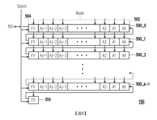
在一實施例中,不同區塊的位元線可能因不同的設計方式而由不同的可編程電流比較器進行測試。如圖6所示,半導體記憶體裝置600包括列解碼器610、第一電壓泵電路620_1、第二電壓泵電路620_2、第一可編程電流比較器630_1、第二可編程電流比較器630_2以及或閘640。In one embodiment, bit lines of different blocks may be tested by different programmable current comparators due to different design methods. As shown in FIG6 , a
列解碼器610耦接於第一可編程電流比較器630_1所對應的多條字元線與第一測試路徑TP1之間,且耦接於第二可編程電流比較器630_2所對應的多條字元線與第二測試路徑TP2之間。列解碼器610可對列位址資料ADD進行解碼,並根據解碼結果將對應的字元線作為測試字元線WLt來與第一測試路徑TP1或第二測試路徑TP2電性連接。The
第一電壓泵電路620_1配置在測試路徑TP1上。第一電壓泵電路620_1可接收操作電壓Vt1並加以調整,以施加測試電壓Vpp1至與第一測試路徑TP1電性連接的測試字元線WLt。The first voltage pump circuit 620_1 is disposed on the test path TP1. The first voltage pump circuit 620_1 can receive the operation voltage Vt1 and adjust it to apply the test voltage Vpp1 to the test word line WLt electrically connected to the first test path TP1.
第二電壓泵電路620_2配置在測試路徑TP2上。第二電壓泵電路620_2可接收操作電壓Vt2並加以調整,以施加測試電壓Vpp2至與第二測試路徑TP2電性連接的測試字元線WLt。The second voltage pump circuit 620_2 is disposed on the test path TP2. The second voltage pump circuit 620_2 can receive the operation voltage Vt2 and adjust it to apply the test voltage Vpp2 to the test word line WLt electrically connected to the second test path TP2.
第一可編程電流比較器630_1耦接第一測試路徑TP1。第一可編程電流比較器630_1可根據所接收到的供應電壓Vs,傳送操作電壓Vt1至第一電壓泵電路620_1。並且,第一可編程電流比較器630_1可將流經第一測試路徑TP1的測試電流Ivpp1與對應的可編程參考電流進行比較,以輸出第一測試結果信號Dout1至或閘640。The first programmable current comparator 630_1 is coupled to the first test path TP1. The first programmable current comparator 630_1 can transmit the operating voltage Vt1 to the first voltage pump circuit 620_1 according to the received supply voltage Vs. In addition, the first programmable current comparator 630_1 can compare the test current Ivpp1 flowing through the first test path TP1 with the corresponding programmable reference current to output the first test result signal Dout1 to the
第二可編程電流比較器630_2耦接第二測試路徑TP2。第二可編程電流比較器630_2可根據所接收到的供應電壓Vs,傳送操作電壓Vt2至第二電壓泵電路620_2。並且,第二可編程電流比較器630_2可將流經第二測試路徑TP2的測試電流Ivpp2與對應的可編程參考電流進行比較,以輸出第二測試結果信號Dout2至或閘640。The second programmable current comparator 630_2 is coupled to the second test path TP2. The second programmable current comparator 630_2 can transmit the operating voltage Vt2 to the second voltage pump circuit 620_2 according to the received supply voltage Vs. In addition, the second programmable current comparator 630_2 can compare the test current Ivpp2 flowing through the second test path TP2 with the corresponding programmable reference current to output the second test result signal Dout2 to the
或閘640的第一輸入端接收來自第一可編程電流比較器630_1的第一測試結果信號Dout1,第二輸入端接收來自第二可編程電流比較器630_2的第二測試結果信號Dout2,輸出端提供測試結果信號Dout。藉由上述所說明的電路結構,能夠在半導體記憶體裝置設置多個可編程電流比較器,藉以對不同區塊的位元線進行測試。The first input terminal of the
需說明的是,根據不同的設計方式,第一可編程電流比較器630_1與第二可編程電流比較器630_2所預設的等效電阻Rsen可以相同或不同。第一可編程電流比較器630_1與第二可編程電流比較器630_2所接收到的供應電壓Vs也可以相同或不同。此外,列解碼器610可以拆分成多個解碼器,以分別耦接不同的測試路徑來對所對應的多條字元線進行測試。It should be noted that, according to different design methods, the preset equivalent resistance Rsen of the first programmable current comparator 630_1 and the second programmable current comparator 630_2 can be the same or different. The supply voltage Vs received by the first programmable current comparator 630_1 and the second programmable current comparator 630_2 can also be the same or different. In addition, the
再者,雖然本實施例是以包括2個電壓泵電路及2個可編程電流比較器的半導體記憶體裝置進行說明,但上述元件的個數並不用以限定本發明。本領域技術人員可以視其實際需求,並參照本實施例之教示,而將上述元件的個數類推至更多。Furthermore, although the present embodiment is described with reference to a semiconductor memory device including two voltage pump circuits and two programmable current comparators, the number of the above components is not intended to limit the present invention. Those skilled in the art can, according to their actual needs and with reference to the teachings of the present embodiment, extrapolate the number of the above components to a greater number.
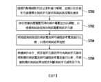
請參照圖7,在本實施例中半導體記憶體裝置的測試方法包括下列步驟。透過列解碼器對列位址資料進行解碼,並據以從多個字元線選擇出測試字元線來與測試路徑電性連接(步驟S700)。接收根據供應電壓而得的操作電壓並加以調整,以透過測試路徑施加測試電壓測試字元線(步驟S702)。將流經測試路徑的測試電流與可編程參考電流進行比較,以提供測試結果信號(步驟S704)。根據操作命令,將多個字元線依序作為測試字元線來將對應的測試電流與可編程參考電流進行比較,而根據對應的測試結果信號來判斷測試字元線是否不良(步驟S706)。上述步驟S700、S702、S704及S706的實施細節可參照圖1至圖6的實施例,在此則不再贅述。Referring to FIG. 7 , in the present embodiment, the semiconductor memory device testing method includes the following steps. Decoding the column address data through the column decoder, and selecting a test word line from a plurality of word lines to electrically connect to the test path (step S700). Receiving and adjusting the operating voltage obtained according to the supply voltage to apply the test voltage through the test path to test the word line (step S702). Comparing the test current flowing through the test path with the programmable reference current to provide a test result signal (step S704). According to the operation command, multiple word lines are sequentially used as test word lines to compare the corresponding test current with the programmable reference current, and whether the test word line is defective is determined according to the corresponding test result signal (step S706). The implementation details of the above steps S700, S702, S704 and S706 can refer to the embodiments of Figures 1 to 6, and will not be repeated here.
需說明的是,雖然本實施例的測試方法主要針對字元線漏電流,但本發明並不以此為限,通過適當的時序安排及所需的電壓設置還可以適用於字元線上其他種類的漏檢測。It should be noted that although the testing method of this embodiment is mainly aimed at word line leakage current, the present invention is not limited thereto and can also be applied to other types of leakage detection on word lines through appropriate timing arrangement and required voltage setting.
綜上所述,本發明的半導體記憶體裝置及其測試方法能夠將針對高阻抗的字元線漏電流的測試簡化為在功能性測試中進行,無需額外進行直流測試。如此一來,不僅可大幅降低測試時間,還能夠將其導入至量產的標準測試項目中來過濾掉不良的元件,提高產品的可靠度。In summary, the semiconductor memory device and its testing method of the present invention can simplify the test of high-impedance word line leakage current to be performed during functional testing, without the need for additional DC testing. In this way, not only can the test time be greatly reduced, but it can also be introduced into the standard test items of mass production to filter out defective components and improve product reliability.
100、600:半導體記憶體裝置 110、610:列解碼器 120:電壓泵電路 130:可編程電流比較器 140:控制電路 150:列位址鎖存器 160:刷新計數器 500_0~500_k-1:移位暫存器 502:多個位址位元 504:有效位元 510:溢位暫存器 620_1:第一電壓泵電路 620_2:第二電壓泵電路 630_1:第一可編程電流比較器 630_2:第二可編程電流比較器 640:或閘 A0~Aj-1:二進位值 ADD:列位址資料 Badd:不良列位址 BL0~BLm-1、BL*0~BL*m-1:位元線 CLK:時脈信號 CMD:操作命令 CMP1:第一比較器 CMP2:第二比較器 Dout:測試結果信號 Dout1:第一測試結果信號 Dout2:第二測試結果信號 FO:溢位旗標 FV:有效旗標 Id:電流 Ivpp、Ivpp1、Ivpp1:測試電流 MC:記憶體胞元 Nin:輸入節點 Nout:輸出節點 R1:第一電阻 R2:第二電阻 R3:第三電阻 R4:第四電阻 R5:第五電阻 R6:第六電阻 Scomp:執行脈衝信號 Slatch:鎖存脈衝信號 Sset:設定信號 Sset1:第一設定信號 Sset2:第二設定信號 Sset3:第三設定信號 Sset4:第四設定信號 SW1:第一開關 SW2:第二開關 SW3:第三開關 SW4:第四開關 t1~t4:時間點 TDO:輸出腳位 TP:測試路徑 TP1:第一測試路徑 TP2:第二測試路徑 Ts:偵測時間 Vout:電壓 Vpp、Vpp1、Vpp2:測試電壓 Vs:供應電壓 Vt、Vt1、Vt2:操作電壓 WL0~WLn-1、WLi、WLi-1、WLi+1:字元線 WLt:測試字元線 S300~S310、S700~S706:步驟100, 600: semiconductor memory device110, 610: column decoder120: voltage pump circuit130: programmable current comparator140: control circuit150: column address latch160: refresh counter500_0~500_k-1: shift register502: multiple address bits504: valid bit510: overflow register620_1: first voltage pump circuit620_2: second voltage pump circuit630_1: first programmable current comparator630_2: second programmable current comparator640: OR gateA0~Aj-1: binary valueADD: row address dataBadd: bad row addressBL0~BLm-1, BL*0~BL*m-1: bit lineCLK: clock signalCMD: operation commandCMP1: first comparatorCMP2: second comparatorDout: test result signalDout1: first test result signalDout2: second test result signalFO: overflow flagFV: valid flagId: currentIvpp, Ivpp1, Ivpp1: test currentMC: memory cellNin: input nodeNout: output nodeR1: first resistorR2: second resistorR3: third resistorR4: fourth resistorR5: fifth resistorR6: sixth resistorScomp: execution pulse signalSlatch: latch pulse signalSset: setting signalSset1: first setting signalSset2: second setting signalSset3: third setting signalSset4: fourth setting signalSW1: first switchSW2: second switchSW3: third switchSW4: fourth switcht1~t4: time pointTDO: output pinTP: test pathTP1: first test pathTP2: second test pathTs: detection timeVout: voltageVpp, Vpp1, Vpp2: test voltageVs: supply voltageVt, Vt1, Vt2: operating voltageWL0~WLn-1, WLi, WLi-1, WLi+1: word lineWLt: Test character lineS300~S310, S700~S706: Steps
圖1是依照本發明一實施例的半導體記憶體裝置的電路示意圖。 圖2是依照本發明一實施例的可編程電流比較器的電路示意圖。 圖3是依照本發明一實施例的半導體記憶體裝置的測試操作的流程圖。 圖4是依照本發明一實施例的半導體記憶體裝置的測試操作的波形示意圖。 圖5是依照本發明一實施例的列位址鎖存器的架構示意圖。 圖6是依照本發明另一實施例的半導體記憶體裝置的部分電路示意圖 圖7是依照本發明一實施例的半導體記憶體裝置的測試方法的流程圖。FIG. 1 is a circuit diagram of a semiconductor memory device according to an embodiment of the present invention.FIG. 2 is a circuit diagram of a programmable current comparator according to an embodiment of the present invention.FIG. 3 is a flow chart of a test operation of a semiconductor memory device according to an embodiment of the present invention.FIG. 4 is a waveform diagram of a test operation of a semiconductor memory device according to an embodiment of the present invention.FIG. 5 is a schematic diagram of the structure of a column address latch according to an embodiment of the present invention.FIG. 6 is a partial circuit diagram of a semiconductor memory device according to another embodiment of the present invention.FIG. 7 is a flow chart of a test method of a semiconductor memory device according to an embodiment of the present invention.
100:半導體記憶體裝置100:Semiconductor memory device
110:列解碼器110: Column decoder
120:電壓泵電路120: Voltage pump circuit
130:可編程電流比較器130: Programmable current comparator
140:控制電路140: Control circuit
150:列位址鎖存器150: Column address latch
160:刷新計數器160: Refresh counter
ADD:列位址資料ADD: column address data
Badd:不良列位址Badd: Bad column address
BL0~BLm-1、BL*0~BL*m-1:位元線BL0~BLm-1, BL*0~BL*m-1: bit line
CMD:操作命令CMD: Operation command
Dout:測試結果信號Dout: test result signal
Ivpp:測試電流Ivpp: test current
MC:記憶體胞元MC: memory cell
Scomp:執行脈衝信號Scomp: Execution pulse signal
Slatch:鎖存脈衝信號Slatch: latch pulse signal
Sset:設定信號Sset: Set signal
TP:測試路徑TP: Test path
Vpp:測試電壓Vpp: test voltage
Vs:供應電壓Vs: Supply voltage
Vt:操作電壓Vt: operating voltage
WL0~WLn-1:字元線WL0~WLn-1: character line
WLt:測試字元線WLt: Test character line
Claims (13)
Translated fromChinesePriority Applications (3)
| Application Number | Priority Date | Filing Date | Title |
|---|---|---|---|
| TW112139363ATWI881494B (en) | 2023-10-16 | 2023-10-16 | Semiconductor memory device and testing method thereof |
| CN202311580738.5ACN119851731A (en) | 2023-10-16 | 2023-11-24 | Semiconductor memory device and test method thereof |
| US18/826,151US20250124996A1 (en) | 2023-10-16 | 2024-09-05 | Semiconductor memory device and test method thereof |
Applications Claiming Priority (1)
| Application Number | Priority Date | Filing Date | Title |
|---|---|---|---|
| TW112139363ATWI881494B (en) | 2023-10-16 | 2023-10-16 | Semiconductor memory device and testing method thereof |
Publications (2)
| Publication Number | Publication Date |
|---|---|
| TWI881494Btrue TWI881494B (en) | 2025-04-21 |
| TW202518460A TW202518460A (en) | 2025-05-01 |
Family
ID=95341002
Family Applications (1)
| Application Number | Title | Priority Date | Filing Date |
|---|---|---|---|
| TW112139363ATWI881494B (en) | 2023-10-16 | 2023-10-16 | Semiconductor memory device and testing method thereof |
Country Status (3)
| Country | Link |
|---|---|
| US (1) | US20250124996A1 (en) |
| CN (1) | CN119851731A (en) |
| TW (1) | TWI881494B (en) |
Citations (1)
| Publication number | Priority date | Publication date | Assignee | Title |
|---|---|---|---|---|
| US20100125429A1 (en)* | 2008-11-14 | 2010-05-20 | Micron Technology, Inc. | Automatic word line leakage measurement circuitry |
- 2023
- 2023-10-16TWTW112139363Apatent/TWI881494B/enactive
- 2023-11-24CNCN202311580738.5Apatent/CN119851731A/enactivePending
- 2024
- 2024-09-05USUS18/826,151patent/US20250124996A1/enactivePending
Patent Citations (1)
| Publication number | Priority date | Publication date | Assignee | Title |
|---|---|---|---|---|
| US20100125429A1 (en)* | 2008-11-14 | 2010-05-20 | Micron Technology, Inc. | Automatic word line leakage measurement circuitry |
Also Published As
| Publication number | Publication date |
|---|---|
| TW202518460A (en) | 2025-05-01 |
| US20250124996A1 (en) | 2025-04-17 |
| CN119851731A (en) | 2025-04-18 |
Similar Documents
| Publication | Publication Date | Title |
|---|---|---|
| US10074443B2 (en) | Semiconductor device including fuse circuit | |
| TWI618074B (en) | One time programmable non-volatile memory and associated read sensing method | |
| US6983404B2 (en) | Method and apparatus for checking the resistance of programmable elements | |
| US20090059682A1 (en) | Semiconductor memory device having antifuse circuitry | |
| US20170110200A1 (en) | Memory device and operating method thereof | |
| KR100985400B1 (en) | Method and circuit for identifying weak bits in a magnetoresistive random access memory | |
| US8599635B2 (en) | Fuse circuit and semiconductor memory device including the same | |
| KR100416919B1 (en) | Circuit and method for accessing momory cells of a memory device | |
| US7859938B2 (en) | Semiconductor memory device and test method thereof | |
| KR100824141B1 (en) | Semiconductor memory device | |
| JP2004039221A (en) | On-chip compression of charge distribution data | |
| JP2014220026A (en) | Semiconductor device and method of switching data line | |
| TWI881494B (en) | Semiconductor memory device and testing method thereof | |
| US5710737A (en) | Semiconductor memory device | |
| US10068662B2 (en) | Semiconductor device including a roll call circuit for outputting addresses of defective memory cells | |
| US8391083B2 (en) | Semiconductor device capable of detecting defect of column selection line | |
| JP2008004264A (en) | Nonvolatile semiconductor memory and method for detecting and replacing defective column in nonvolatile semiconductor memory | |
| JP3762517B2 (en) | Burn-in stress circuit for semiconductor memory device | |
| US11335427B1 (en) | Memory test circuit | |
| US7791960B2 (en) | Semiconductor memory device and control signal generating method thereof | |
| US6434070B1 (en) | Semiconductor integrated circuit with variable bit line precharging voltage | |
| CN110827878B (en) | memory device | |
| US6256257B1 (en) | Memory device including a burn-in controller for enabling multiple wordiness during wafer burn-in | |
| KR100357187B1 (en) | Circuit of Semiconductor Memory | |
| US20040141387A1 (en) | Semiconductor storage device |