TWI879590B - Potential conversion circuit, source drive circuit, display and information processing device - Google Patents
Potential conversion circuit, source drive circuit, display and information processing deviceDownload PDFInfo
- Publication number
- TWI879590B TWI879590BTW113120299ATW113120299ATWI879590BTW I879590 BTWI879590 BTW I879590BTW 113120299 ATW113120299 ATW 113120299ATW 113120299 ATW113120299 ATW 113120299ATW I879590 BTWI879590 BTW I879590B
- Authority
- TW
- Taiwan
- Prior art keywords
- source
- drain
- gate
- coupled
- nmos transistor
- Prior art date
Links
Images


Landscapes
- Logic Circuits (AREA)
Abstract
Translated fromChineseDescription
Translated fromChinese本發明係有關顯示器驅動電路,尤指一種源極驅動器之電位轉換電路。The present invention relates to a display driver circuit, and more particularly to a potential conversion circuit of a source driver.
隨著市場需求的演變,顯示器的應用產品已從電視、筆電、手機、手錶擴展到VR(虛擬實像)眼鏡及AR(擴增實像)眼鏡,而在VR(虛擬實像)眼鏡及AR(擴增實像)眼鏡的高解析顯示應用中,由於電路板的面積有限,顯示器的源極驅動電路不能靠多顆驅動晶片串接而必須在單顆驅動晶片裡提供高數目的輸出通道來滿足高解析度的顯示需求。With the evolution of market demand, the application products of displays have expanded from TVs, laptops, mobile phones, and watches to VR (virtual reality) glasses and AR (augmented reality) glasses. In the high-resolution display applications of VR (virtual reality) glasses and AR (augmented reality) glasses, due to the limited area of the circuit board, the source driver circuit of the display cannot rely on multiple driver chips connected in series, but must provide a large number of output channels in a single driver chip to meet the high-resolution display requirements.
請參照圖1,其為一現有源極驅動晶片之一輸出通道之方塊圖。如圖1所示,該輸出通道具有一移位暫存器10、一電位轉換電路20、一數位至類比轉換電路30及一緩衝放大器40,其中,移位暫存器10係用以儲存以序列方式輸入之一顯示資料DIN並以並列的格式輸出該顯示資料DIN;電位轉換電路20係用以提高該顯示資料DIN的邏輯準位以輸出一對應的數位信號;數位至類比轉換電路30係用以依該對應的數位信號產生一類比電壓;以及緩衝放大器40係用以依該類比電壓產生一輸出電壓VOUT以驅動一顯示器。Please refer to FIG1, which is a block diagram of an output channel of a conventional active-source driver chip. As shown in FIG1, the output channel has a
請參照圖2,其繪示圖1之電位轉換電路20之電路圖。如圖2所示,電位轉換電路20,耦接於一正供應電壓VDD與一參考地之間,具有一對主動負載(由一PMOS電晶體21a和一PMOS電晶體21b組成)、一閂鎖電路(由一PMOS電晶體22a和一PMOS電晶體22b組成)、一對疊接負載(由一NMOS電晶體23a和一NMOS電晶體23b組成)以及一對反相器(由一NMOS電晶體24a和一NMOS電晶體24b組成),其中,PMOS電晶體21a之閘極和PMOS電晶體21b之閘極共同耦接一第一直流電壓VBP,NMOS電晶體23a之閘極和NMOS電晶體23b之閘極共同耦接一第二直流電壓VBN,NMOS電晶體24a之閘極耦接一正輸入信號VIP,NMOS電晶體24b之閘極耦接一負輸入信號VIN,且NMOS電晶體24a之源極和NMOS電晶體24b之源極耦接至一接地節點GND,接地節點GND再經由一導電路徑連接至該參考地。於操作時,當正輸入信號VIP為邏輯1,節點QB的電位會被拉低,致使PMOS電晶體22b導通而將節點Q的電位拉高;當負輸入信號VIN為邏輯1,節點Q的電位會被拉低,致使PMOS電晶體22a導通而將節點QB的電位拉高。Please refer to FIG. 2, which shows a circuit diagram of the
然而,在多個輸出通道同時操作時,該些輸出通道之瞬間電流的總和卻會在接地節點GND與該參考地之間產生壓降(亦即在接地節點GND與該參考地之間的路徑電阻上產生一電壓),致使NMOS電晶體24a和NMOS電晶體24b無法正常操作,從而導致電位轉換電路20的輸出異常。However, when multiple output channels operate simultaneously, the sum of the instantaneous currents of the output channels will generate a voltage drop between the ground node GND and the reference ground (i.e., a voltage is generated on the path resistance between the ground node GND and the reference ground), causing the
為解決上述的問題,本領域亟需一種新穎的電位轉換電路。In order to solve the above problems, a novel potential conversion circuit is urgently needed in this field.
本發明之主要目的在於提供一種電位轉換電路,其可在一電位轉換操作的過程中暫時將其低側反相電路對與高側主動負載對斷開,以有效降低其接地節點與參考地之間之電位差,從而確保該電位轉換操作的正確性和可靠度。The main purpose of the present invention is to provide a potential conversion circuit which can temporarily disconnect its low-side inverter circuit pair from its high-side active load pair during a potential conversion operation to effectively reduce the potential difference between its ground node and the reference ground, thereby ensuring the accuracy and reliability of the potential conversion operation.
本發明之另一目的在於提供一種電位轉換電路,其可在該電位轉換操作的過程中先使其正、負輸出節點的電位均預充至一正供應電壓,從而有效提升該電位轉換操作的反應速度。Another object of the present invention is to provide a potential conversion circuit which can pre-charge the potentials of both the positive and negative output nodes to a positive supply voltage during the potential conversion operation, thereby effectively improving the response speed of the potential conversion operation.
為達上述目的,一種電位轉換電路乃被提出,其具有: 一第一PMOS電晶體和一第二PMOS電晶體,其中,該第一PMOS電晶體具有一第一源極、一第一閘極和一第一汲極,該第一源極係用以耦接一正供應電壓,該第一閘極係用以耦接一第一直流電壓;及該第二PMOS電晶體具有一第二源極、一第二閘極和一第二汲極,該第二源極係用以耦接該正供應電壓,該第二閘極係用以耦接該第一直流電壓; 一第三PMOS電晶體和一第四PMOS電晶體,其中,該第三PMOS電晶體具有一第三源極、一第三閘極和一第三汲極,該第三源極耦接該第一汲極,該第三閘極耦接一正輸出節點,該第三汲極耦接一負輸出節點;及該第四PMOS電晶體具有一第四源極、一第四閘極和一第四汲極,該第四源極係用以耦接該第二汲極,該第四閘極耦接該負輸出節點,該第四汲極耦接該正輸出節點; 一第一NMOS電晶體和一第二NMOS電晶體,其中,該第一NMOS電晶體具有一第五汲極、一第五閘極和一第五源極,該第五汲極耦接該負輸出節點,該第五閘極耦接一第一致能信號;及該第二NMOS電晶體具有一第六汲極、一第六閘極和一第六源極,該第六汲極耦接該正輸出節點,該第六閘極耦接該第一致能信號; 一第三NMOS電晶體和一第四NMOS電晶體,其中,該第三NMOS電晶體具有一第七汲極、一第七閘極和一第七源極,該第七汲極耦接該第五源極,該第七閘極耦接一第二直流電壓;及該第四NMOS電晶體具有一第八汲極、一第八閘極和一第八源極,該第八汲極耦接該第六源極,該第八閘極耦接該第二直流電壓; 一第五NMOS電晶體和一第六NMOS電晶體,其中,該第五NMOS電晶體具有一第九汲極、一第九閘極和一第九源極,該第九汲極耦接該第七源極,該第九閘極耦接一正輸入信號,該第九源極耦接一接地節點;及該第六NMOS電晶體具有一第十汲極、一第十閘極和一第十源極,該第十汲極耦接該第八源極,該第十閘極耦接一負輸入信號,該第十源極耦接該接地節點;以及 一第五PMOS電晶體和一第六PMOS電晶體,其中,該第五PMOS電晶體具有一第十一源極、一第十一閘極和一第十一汲極,該第十一源極耦接該正供應電壓,該第十一閘極係用以耦接一第二致能信號,該第十一汲極耦接該負輸出節點;及該第六PMOS電晶體具有一第十二源極、一第十二閘極和一第十二汲極,該第十二源極耦接該正供應電壓,該第十二閘極係用以耦接該第二致能信號,該第十二汲極耦接該正輸出節點。To achieve the above-mentioned purpose, a potential conversion circuit is proposed, which has:A first PMOS transistor and a second PMOS transistor, wherein the first PMOS transistor has a first source, a first gate and a first drain, the first source is used to couple a positive supply voltage, and the first gate is used to couple a first DC voltage; and the second PMOS transistor has a second source, a second gate and a second drain, the second source is used to couple the positive supply voltage, and the second gate is used to couple the first DC voltage;A third PMOS transistor and a fourth PMOS transistor, wherein the third PMOS transistor has a third source, a third gate and a third drain, the third source is coupled to the first drain, the third gate is coupled to a positive output node, and the third drain is coupled to a negative output node; and the fourth PMOS transistor has a fourth source, a fourth gate and a fourth drain, the fourth source is used to couple the second drain, the fourth gate is coupled to the negative output node, and the fourth drain is coupled to the positive output node;A first NMOS transistor and a second NMOS transistor, wherein the first NMOS transistor has a fifth drain, a fifth gate and a fifth source, the fifth drain is coupled to the negative output node, and the fifth gate is coupled to a first enable signal; and the second NMOS transistor has a sixth drain, a sixth gate and a sixth source, the sixth drain is coupled to the positive output node, and the sixth gate is coupled to the first enable signal;A third NMOS transistor and a fourth NMOS transistor, wherein the third NMOS transistor has a seventh drain, a seventh gate and a seventh source, the seventh drain is coupled to the fifth source, and the seventh gate is coupled to a second DC voltage; and the fourth NMOS transistor has an eighth drain, an eighth gate and an eighth source, the eighth drain is coupled to the sixth source, and the eighth gate is coupled to the second DC voltage;a fifth NMOS transistor and a sixth NMOS transistor, wherein the fifth NMOS transistor has a ninth drain, a ninth gate and a ninth source, the ninth drain is coupled to the seventh source, the ninth gate is coupled to a positive input signal, and the ninth source is coupled to a ground node; and the sixth NMOS transistor has a tenth drain, a tenth gate and a tenth source, the tenth drain is coupled to the eighth source, the tenth gate is coupled to a negative input signal, and the tenth source is coupled to the ground node; andA fifth PMOS transistor and a sixth PMOS transistor, wherein the fifth PMOS transistor has an eleventh source, an eleventh gate and an eleventh drain, the eleventh source is coupled to the positive supply voltage, the eleventh gate is used to couple a second enable signal, and the eleventh drain is coupled to the negative output node; and the sixth PMOS transistor has a twelfth source, a twelfth gate and a twelfth drain, the twelfth source is coupled to the positive supply voltage, the twelfth gate is used to couple the second enable signal, and the twelfth drain is coupled to the positive output node.
在一實施例中,該第一致能信號和該第二致能信號係由一時序控制單元提供。In one embodiment, the first enable signal and the second enable signal are provided by a timing control unit.
在一實施例中,該正輸入信號和該負輸入信號係由一移位暫存器提供,且該移位暫存器係依該時序控制單元所提供之一顯示資料產生該正輸入信號和該負輸入信號。In one embodiment, the positive input signal and the negative input signal are provided by a shift register, and the shift register generates the positive input signal and the negative input signal according to a display data provided by the timing control unit.
在一實施例中,所述之電位轉換電路係依該第一致能信號和該第二致能信號之控制進行一電位轉換操作,且該電位轉換操作之特徵在於: 該第一致能信號係在該正輸入信號和該負輸入信號輸入前先斷開該第一NMOS電晶體和該第二NMOS電晶體,且該第二致能信號係在該第一NMOS電晶體和該第二NMOS電晶體被斷開後導通該第五PMOS電晶體和該第六PMOS電晶體以將該正輸出節點和該負輸出節點拉升至該正供應電壓。In one embodiment, the potential conversion circuit performs a potential conversion operation according to the control of the first enable signal and the second enable signal, and the potential conversion operation is characterized in that: The first enable signal disconnects the first NMOS transistor and the second NMOS transistor before the positive input signal and the negative input signal are input, and the second enable signal turns on the fifth PMOS transistor and the sixth PMOS transistor after the first NMOS transistor and the second NMOS transistor are disconnected to pull the positive output node and the negative output node to the positive supply voltage.
亦即,本發明揭露了一種電位轉換電路,其具有一對低側反相電路及一對高側閂鎖式主動負載以對一正輸入信號和一負輸入信號進行一電位轉換操作,該對低側反相電路及該對高側閂鎖式主動負載之間具有一正輸出節點及一負輸出節點,且該電位轉換電路之特徵在於:在該電位轉換操作中,利用一對第一開關暫時斷開該對低側反相電路與該對高側主動負載之間的電流路徑,以及利用一對第二開關先使該正輸出節點及該負輸出節點的電位均預充至一正供應電壓。That is, the present invention discloses a potential conversion circuit, which has a pair of low-side inverter circuits and a pair of high-side latched active loads to perform a potential conversion operation on a positive input signal and a negative input signal, and there is a positive output node and a negative output node between the pair of low-side inverter circuits and the pair of high-side latched active loads, and the potential conversion circuit is characterized in that: in the potential conversion operation, a pair of first switches are used to temporarily disconnect the current path between the pair of low-side inverter circuits and the pair of high-side active loads, and a pair of second switches are used to pre-charge the potentials of the positive output node and the negative output node to a positive supply voltage.
為達上述目的,本發明進一步提出一種源極驅動電路,其具有多個輸出通道,各該輸出通道均具有一電位轉換電路,且該電位轉換電路具有: 一第一PMOS電晶體和一第二PMOS電晶體,其中,該第一PMOS電晶體具有一第一源極、一第一閘極和一第一汲極,該第一源極係用以耦接一正供應電壓,該第一閘極係用以耦接一第一直流電壓;及該第二PMOS電晶體具有一第二源極、一第二閘極和一第二汲極,該第二源極係用以耦接該正供應電壓,該第二閘極係用以耦接該第一直流電壓; 一第三PMOS電晶體和一第四PMOS電晶體,其中,該第三PMOS電晶體具有一第三源極、一第三閘極和一第三汲極,該第三源極耦接該第一汲極,該第三閘極耦接一正輸出節點,該第三汲極耦接一負輸出節點;及該第四PMOS電晶體具有一第四源極、一第四閘極和一第四汲極,該第四源極係用以耦接該第二汲極,該第四閘極耦接該負輸出節點,該第四汲極耦接該正輸出節點; 一第一NMOS電晶體和一第二NMOS電晶體,其中,該第一NMOS電晶體具有一第五汲極、一第五閘極和一第五源極,該第五汲極耦接該負輸出節點,該第五閘極耦接一第一致能信號;及該第二NMOS電晶體具有一第六汲極、一第六閘極和一第六源極,該第六汲極耦接該正輸出節點,該第六閘極耦接該第一致能信號; 一第三NMOS電晶體和一第四NMOS電晶體,其中,該第三NMOS電晶體具有一第七汲極、一第七閘極和一第七源極,該第七汲極耦接該第五源極,該第七閘極耦接一第二直流電壓;及該第四NMOS電晶體具有一第八汲極、一第八閘極和一第八源極,該第八汲極耦接該第六源極,該第八閘極耦接該第二直流電壓; 一第五NMOS電晶體和一第六NMOS電晶體,其中,該第五NMOS電晶體具有一第九汲極、一第九閘極和一第九源極,該第九汲極耦接該第七源極,該第九閘極耦接一正輸入信號,該第九源極耦接一接地節點;及該第六NMOS電晶體具有一第十汲極、一第十閘極和一第十源極,該第十汲極耦接該第八源極,該第十閘極耦接一負輸入信號,該第十源極耦接該接地節點;以及 一第五PMOS電晶體和一第六PMOS電晶體,其中,該第五PMOS電晶體具有一第十一源極、一第十一閘極和一第十一汲極,該第十一源極耦接該正供應電壓,該第十一閘極係用以耦接一第二致能信號,該第十一汲極耦接該負輸出節點;及該第六PMOS電晶體具有一第十二源極、一第十二閘極和一第十二汲極,該第十二源極耦接該正供應電壓,該第十二閘極係用以耦接該第二致能信號,該第十二汲極耦接該正輸出節點。To achieve the above-mentioned purpose, the present invention further proposes a source drive circuit having a plurality of output channels, each of which has a potential conversion circuit, and the potential conversion circuit has: A first PMOS transistor and a second PMOS transistor, wherein the first PMOS transistor has a first source, a first gate and a first drain, the first source is used to couple a positive supply voltage, and the first gate is used to couple a first DC voltage; and the second PMOS transistor has a second source, a second gate and a second drain, the second source is used to couple the positive supply voltage, and the second gate is used to couple the first DC voltage; A third PMOS transistor and a fourth PMOS transistor, wherein the third PMOS transistor has a third source, a third gate and a third drain, the third source is coupled to the first drain, the third gate is coupled to a positive output node, and the third drain is coupled to a negative output node; and the fourth PMOS transistor has a fourth source, a fourth gate and a fourth drain, the fourth source is used to couple the second drain, the fourth gate is coupled to the negative output node, and the fourth drain is coupled to the positive output node;A first NMOS transistor and a second NMOS transistor, wherein the first NMOS transistor has a fifth drain, a fifth gate and a fifth source, the fifth drain is coupled to the negative output node, and the fifth gate is coupled to a first enable signal; and the second NMOS transistor has a sixth drain, a sixth gate and a sixth source, the sixth drain is coupled to the positive output node, and the sixth gate is coupled to the first enable signal;A third NMOS transistor and a fourth NMOS transistor, wherein the third NMOS transistor has a seventh drain, a seventh gate and a seventh source, the seventh drain is coupled to the fifth source, and the seventh gate is coupled to a second DC voltage; and the fourth NMOS transistor has an eighth drain, an eighth gate and an eighth source, the eighth drain is coupled to the sixth source, and the eighth gate is coupled to the second DC voltage;a fifth NMOS transistor and a sixth NMOS transistor, wherein the fifth NMOS transistor has a ninth drain, a ninth gate and a ninth source, the ninth drain is coupled to the seventh source, the ninth gate is coupled to a positive input signal, and the ninth source is coupled to a ground node; and the sixth NMOS transistor has a tenth drain, a tenth gate and a tenth source, the tenth drain is coupled to the eighth source, the tenth gate is coupled to a negative input signal, and the tenth source is coupled to the ground node; andA fifth PMOS transistor and a sixth PMOS transistor, wherein the fifth PMOS transistor has an eleventh source, an eleventh gate and an eleventh drain, the eleventh source is coupled to the positive supply voltage, the eleventh gate is used to couple a second enable signal, and the eleventh drain is coupled to the negative output node; and the sixth PMOS transistor has a twelfth source, a twelfth gate and a twelfth drain, the twelfth source is coupled to the positive supply voltage, the twelfth gate is used to couple the second enable signal, and the twelfth drain is coupled to the positive output node.
在一實施例中,該第一致能信號和該第二致能信號係由一時序控制單元提供。In one embodiment, the first enable signal and the second enable signal are provided by a timing control unit.
在一實施例中,該正輸入信號和該負輸入信號係由一移位暫存器提供,且該移位暫存器係依該時序控制單元所提供之一顯示資料產生該正輸入信號和該負輸入信號。In one embodiment, the positive input signal and the negative input signal are provided by a shift register, and the shift register generates the positive input signal and the negative input signal according to a display data provided by the timing control unit.
在一實施例中,所述之電位轉換電路係依該第一致能信號和該第二致能信號之控制進行一電位轉換操作,且該電位轉換操作之特徵在於: 該第一致能信號係在該正輸入信號和該負輸入信號輸入前先斷開該第一NMOS電晶體和該第二NMOS電晶體,且該第二致能信號係在該第一NMOS電晶體和該第二NMOS電晶體被斷開後導通該第五PMOS電晶體和該第六PMOS電晶體以將該正輸出節點和該負輸出節點拉升至該正供應電壓。In one embodiment, the potential conversion circuit performs a potential conversion operation according to the control of the first enable signal and the second enable signal, and the potential conversion operation is characterized in that: The first enable signal disconnects the first NMOS transistor and the second NMOS transistor before the positive input signal and the negative input signal are input, and the second enable signal turns on the fifth PMOS transistor and the sixth PMOS transistor after the first NMOS transistor and the second NMOS transistor are disconnected to pull the positive output node and the negative output node to the positive supply voltage.
為達上述目的,本發明進一步提出一種顯示器,其包含一顯示面板及用以驅動該顯示面板之如前述之源極驅動電路。To achieve the above object, the present invention further provides a display device, which includes a display panel and the source driving circuit as mentioned above for driving the display panel.
在可能的實施例中,該顯示器可為液晶顯示器、次毫米二極體發光顯示器、微米二極體發光顯示器、量子點二極體發光顯示器或有機發光二極體顯示器。In a possible embodiment, the display may be a liquid crystal display, a sub-millimeter diode light emitting display, a micron diode light emitting display, a quantum dot diode light emitting display or an organic light emitting diode display.
為達上述目的,本發明進一步提出一種資訊處理裝置,其具有一中央處理器及如前述之顯示器,其中,該中央處理器係用以與該顯示器通信。To achieve the above object, the present invention further provides an information processing device having a central processing unit and the display as described above, wherein the central processing unit is used to communicate with the display.
在可能的實施例中,該資訊處理裝置可為攜帶型電腦、車用電腦、智慧型手錶、智慧型手環、智慧型手機、VR眼鏡或AR眼鏡。In a possible embodiment, the information processing device may be a portable computer, a car computer, a smart watch, a smart bracelet, a smart phone, a VR glasses, or an AR glasses.
為使 貴審查委員能進一步瞭解本發明之結構、特徵、目的、與其優點,茲附以圖式及較佳具體實施例之詳細說明如後。In order to enable the Review Committee to further understand the structure, features, purpose, and advantages of the present invention, the following are attached with drawings and detailed descriptions of preferred specific embodiments.
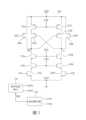
請參照圖3,其繪示本發明之電位轉換電路之一實施例之電路圖。Please refer to FIG. 3 , which shows a circuit diagram of an embodiment of the potential conversion circuit of the present invention.
如圖3所示,一電位轉換電路100,耦接於一正供應電壓VDD與一參考地之間,具有一對主動負載(由一PMOS電晶體101a和一PMOS電晶體101b組成)、一閂鎖電路(由一PMOS電晶體102a和一PMOS電晶體102b組成)、一對第一疊接負載(由一NMOS電晶體103a和一NMOS電晶體103b組成)、一對第二疊接負載(由一NMOS電晶體104a和一NMOS電晶體104b組成)、一對反相器(由一NMOS電晶體105a和一NMOS電晶體105b組成)以及一對拉升開關(由一PMOS電晶體106a和一PMOS電晶體106b組成)。另外,電位轉換電路100係依一時序控制單元110輸出之一第一致能信號EN1和一第二致能信號EN2之控制進行一電位轉換操作。As shown in FIG. 3 , a
在該對主動負載中,PMOS電晶體101a之源極和PMOS電晶體101b之源極共同耦接正供應電壓VDD,PMOS電晶體101a之閘極和PMOS電晶體101b之閘極共同耦接一第一直流電壓VBP,PMOS電晶體101a之汲極耦接PMOS電晶體102a之源極,且PMOS電晶體101b之汲極耦接PMOS電晶體102b之源極。In the pair of active loads, the source of the
在該閂鎖電路中,PMOS電晶體102a之源極耦接PMOS電晶體101a之汲極,閘極耦接正輸出節點Q,汲極耦接負輸出節點QB;PMOS電晶體102b之源極耦接PMOS電晶體101b之汲極,閘極耦接負輸出節點QB,汲極耦接正輸出節點Q。In the latch circuit, the source of the
在該對第一疊接負載中,NMOS電晶體103a之汲極耦接負輸出節點QB,閘極耦接第一致能信號EN1,源極耦接NMOS電晶體104a之汲極;NMOS電晶體103b之汲極耦接正輸出節點Q,閘極耦接第一致能信號EN1,源極耦接NMOS電晶體104b之汲極。In the pair of first cascade loads, the drain of
在該對第二疊接負載中,NMOS電晶體104a之汲極耦接NMOS電晶體103a之源極,閘極耦接一第二直流電壓VBN,源極耦接NMOS電晶體105a之汲極;NMOS電晶體104b之汲極耦接NMOS電晶體103b之源極,閘極耦接第二直流電壓VBN,源極耦接NMOS電晶體105b之汲極。In the pair of second cascade loads, the drain of
在該對反相器中,NMOS電晶體105a之汲極耦接NMOS電晶體104a之源極,閘極耦接一正輸入信號VIP,源極耦接一接地節點GND,接地節點GND再經一導電路徑連接至該參考地;NMOS電晶體105b之汲極耦接NMOS電晶體104b之源極,閘極耦接一負輸入信號VIN,源極耦接該接地節點GND。另外,正輸入信號VIP和負輸入信號VIN係由一移位暫存器120提供,且係依時序控制單元110所提供之一顯示資料DIN之二進制值產生。In the pair of inverters, the drain of
在該對拉升開關中,PMOS電晶體106a之源極耦接正供應電壓VDD,閘極耦接第二致能信號EN2,汲極耦接負輸出節點QB;PMOS電晶體106b之源極耦接正供應電壓VDD,閘極耦接第二致能信號EN2,汲極耦接正輸出節點Q。In the pair of pull-up switches, the source of the
於操作時,時序控制單元110在週期性地輸出顯示資料DIN時會對應輸出第一致能信號EN1和第二致能信號EN2以驅使電位轉換電路100進行所述的電位轉換操作。請參照圖4,其為電位轉換電路100之電位轉換操作之時序圖。如圖4所示,各該電位轉換操作之時序由先至後均包括t1、t2、t3、t4、t5等5個時點。During operation, the
在第1個電位轉換操作中:In the first potential conversion operation:
在t1時點:第一致能信號EN1由高電位變低電位,致使NMOS電晶體103a和NMOS電晶體103b被斷開;且第二致能信號EN2維持高電位,致使PMOS電晶體106a和PMOS電晶體106b維持被斷開狀態。At time t1: the first enable signal EN1 changes from high level to low level, causing the
在t2時點:第一致能信號EN1維持低電位,致使NMOS電晶體103a和NMOS電晶體103b維持被斷開狀態;且第二致能信號EN2由高電位變低電位,致使PMOS電晶體106a和PMOS電晶體106b被導通而使節點Q和節點QB的電位被拉高至VDD。At time t2: the first enable signal EN1 maintains a low level, so that the
在t3時點:電位轉換電路100進入一顯示信號接收期間(在此電位轉換操作中,輸入信號VIP為高電位),第一致能信號EN1維持低電位,致使NMOS電晶體103a和NMOS電晶體103b維持被斷開狀態;且第二致能信號EN2維持低電位,致使PMOS電晶體106a和PMOS電晶體106b維持導通狀態而使節點Q和節點QB的電位維持在VDD。At time t3: the
在t4時點:第一致能信號EN1維持低電位,致使NMOS電晶體103a和NMOS電晶體103b維持被斷開狀態;且第二致能信號EN2由低電位變高電位,致使PMOS電晶體106a和PMOS電晶體106b被斷開,此時節點Q和節點QB的電位維持在VDD。At time t4: the first enable signal EN1 maintains a low level, causing the
在t5時點:第一致能信號EN1由低電位變高電位,致使NMOS電晶體103a和NMOS電晶體103b被導通;且第二致能信號EN2維持高電位,致使PMOS電晶體106a和PMOS電晶體106b維持被斷開狀態。此時,電位轉換電路100進入一電位轉換期間,節點Q的電位維持在VDD,而節點QB電位則由VDD被拉低至該參考地。At time t5: the first enable signal EN1 changes from a low potential to a high potential, causing the
在第2個電位轉換操作中:In the second potential conversion operation:
在t1時點:第一致能信號EN1由高電位變低電位,致使NMOS電晶體103a和NMOS電晶體103b被斷開;且第二致能信號EN2維持高電位,致使PMOS電晶體106a和PMOS電晶體106b維持被斷開狀態。At time t1: the first enable signal EN1 changes from high level to low level, causing the
在t2時點:第一致能信號EN1維持低電位,致使NMOS電晶體103a和NMOS電晶體103b維持被斷開狀態;且第二致能信號EN2由高電位變低電位,致使PMOS電晶體106a和PMOS電晶體106b被導通而使節點Q和節點QB的電位被拉高至VDD。At time t2: the first enable signal EN1 maintains a low level, so that the
在t3時點:電位轉換電路100進入一顯示信號接收期間(在此電位轉換操作中,輸入信號VIP高電位變低電位),第一致能信號EN1維持低電位,致使NMOS電晶體103a和NMOS電晶體103b維持被斷開狀態;且第二致能信號EN2維持低電位,致使PMOS電晶體106a和PMOS電晶體106b維持導通狀態而使節點Q和節點QB的電位維持在VDD。At time t3: the
在t4時點:第一致能信號EN1維持低電位,致使NMOS電晶體103a和NMOS電晶體103b維持被斷開狀態;且第二致能信號EN2由低電位變高電位,致使PMOS電晶體106a和PMOS電晶體106b被斷開,此時節點Q和節點QB的電位維持在VDD。At time t4: the first enable signal EN1 maintains a low level, causing the
在t5時點:第一致能信號EN1由低電位變高電位,致使NMOS電晶體103a和NMOS電晶體103b被導通;且第二致能信號EN2維持高電位,致使PMOS電晶體106a和PMOS電晶體106b維持被斷開狀態。此時,電位轉換電路100進入一電位轉換期間,節點Q的電位由VDD被拉低至該參考地,而節點QB電位則維持在VDD。At time t5: the first enable signal EN1 changes from a low potential to a high potential, causing the
依此,本發明即可在各個電位轉換操作中使NMOS電晶體105a和NMOS電晶體105b的通道電流都為0,從而在多個輸出通道同時操作時,有效避免該些輸出通道之瞬間電流的總和在接地節點GND與該參考地之間產生壓降(亦即在接地節點GND與該參考地之間的路徑電阻上產生一電壓),致使NMOS電晶體105a和NMOS電晶體105b無法正常操作,從而導致電位轉換電路100的輸出異常。Accordingly, the present invention can make the channel current of the
由上述的說明可知,本發明揭露了一種電位轉換電路,其具有: 一第一PMOS電晶體和一第二PMOS電晶體,其中,該第一PMOS電晶體具有一第一源極、一第一閘極和一第一汲極,該第一源極係用以耦接一正供應電壓,該第一閘極係用以耦接一第一直流電壓;及該第二PMOS電晶體具有一第二源極、一第二閘極和一第二汲極,該第二源極係用以耦接該正供應電壓,該第二閘極係用以耦接該第一直流電壓;一第三PMOS電晶體和一第四PMOS電晶體,其中,該第三PMOS電晶體具有一第三源極、一第三閘極和一第三汲極,該第三源極耦接該第一汲極,該第三閘極耦接一正輸出節點,該第三汲極耦接一負輸出節點;及該第四PMOS電晶體具有一第四源極、一第四閘極和一第四汲極,該第四源極係用以耦接該第二汲極,該第四閘極耦接該負輸出節點,該第四汲極耦接該正輸出節點;一第一NMOS電晶體和一第二NMOS電晶體,其中,該第一NMOS電晶體具有一第五汲極、一第五閘極和一第五源極,該第五汲極耦接該負輸出節點,該第五閘極耦接一第一致能信號;及該第二NMOS電晶體具有一第六汲極、一第六閘極和一第六源極,該第六汲極耦接該正輸出節點,該第六閘極耦接該第一致能信號;一第三NMOS電晶體和一第四NMOS電晶體,其中,該第三NMOS電晶體具有一第七汲極、一第七閘極和一第七源極,該第七汲極耦接該第五源極,該第七閘極耦接一第二直流電壓;及該第四NMOS電晶體具有一第八汲極、一第八閘極和一第八源極,該第八汲極耦接該第六源極,該第八閘極耦接該第二直流電壓;一第五NMOS電晶體和一第六NMOS電晶體,其中,該第五NMOS電晶體具有一第九汲極、一第九閘極和一第九源極,該第九汲極耦接該第七源極,該第九閘極耦接一正輸入信號,該第九源極耦接一接地節點;及該第六NMOS電晶體具有一第十汲極、一第十閘極和一第十源極,該第十汲極耦接該第八源極,該第十閘極耦接一負輸入信號,該第十源極耦接該接地節點;以及一第五PMOS電晶體和一第六PMOS電晶體,其中,該第五PMOS電晶體具有一第十一源極、一第十一閘極和一第十一汲極,該第十一源極耦接該正供應電壓,該第十一閘極係用以耦接一第二致能信號,該第十一汲極耦接該負輸出節點;及該第六PMOS電晶體具有一第十二源極、一第十二閘極和一第十二汲極,該第十二源極耦接該正供應電壓,該第十二閘極係用以耦接該第二致能信號,該第十二汲極耦接該正輸出節點。From the above description, it can be seen that the present invention discloses a potential conversion circuit, which has: a first PMOS transistor and a second PMOS transistor, wherein the first PMOS transistor has a first source, a first gate and a first drain, the first source is used to couple a positive supply voltage, and the first gate is used to couple a first DC voltage; and the second PMOS transistor has a second source, a second gate and a second drain, The second source is used to couple the positive supply voltage, and the second gate is used to couple the first DC voltage; a third PMOS transistor and a fourth PMOS transistor, wherein the third PMOS transistor has a third source, a third gate and a third drain, the third source is coupled to the first drain, the third gate is coupled to a positive output node, and the third drain The fourth PMOS transistor has a fourth source, a fourth gate and a fourth drain, the fourth source is used to couple the second drain, the fourth gate is coupled to the negative output node, and the fourth drain is coupled to the positive output node; a first NMOS transistor and a second NMOS transistor, wherein the first NMOS transistor has A fifth drain, a fifth gate and a fifth source, the fifth drain is coupled to the negative output node, the fifth gate is coupled to a first enable signal; and the second NMOS transistor has a sixth drain, a sixth gate and a sixth source, the sixth drain is coupled to the positive output node, the sixth gate is coupled to the first enable signal; a third NMOS transistor and a fourth NMOS transistors, wherein the third NMOS transistor has a seventh drain, a seventh gate and a seventh source, the seventh drain is coupled to the fifth source, the seventh gate is coupled to a second DC voltage; and the fourth NMOS transistor has an eighth drain, an eighth gate and an eighth source, the eighth drain is coupled to the sixth source, the eighth gate is coupled to the a second direct current voltage; a fifth NMOS transistor and a sixth NMOS transistor, wherein the fifth NMOS transistor has a ninth drain, a ninth gate and a ninth source, the ninth drain is coupled to the seventh source, the ninth gate is coupled to a positive input signal, and the ninth source is coupled to a ground node; and the sixth NMOS transistor has a tenth drain, a tenth gate and a tenth source, the tenth drain is coupled to the eighth source, the tenth gate is coupled to a negative input signal, and the tenth source is coupled to the ground node; and a fifth PMOS transistor and a sixth PMOS transistor, wherein the fifth PMOS transistor has an eleventh source, an eleventh gate and an eleventh drain, the eleventh source is coupled to the positive supply voltage, the eleventh gate is used to couple a second enable signal, and the eleventh drain is coupled to the negative output node; and the sixth PMOS transistor has a twelfth source, a twelfth gate and a twelfth drain, the twelfth source is coupled to the positive supply voltage, the twelfth gate is used to couple the second enable signal, and the twelfth drain is coupled to the positive output node.
另外,在本發明之電位轉換電路中,該第一致能信號和該第二致能信號係由一時序控制單元提供;該正輸入信號和該負輸入信號係由一移位暫存器提供,且該移位暫存器係依該時序控制單元所提供之一顯示資料產生該正輸入信號和該負輸入信號;且所述之電位轉換電路係依該第一致能信號和該第二致能信號之控制進行一電位轉換操作,且該電位轉換操作之特徵在於:該第一致能信號係在該正輸入信號和該負輸入信號輸入前先斷開該第一NMOS電晶體和該第二NMOS電晶體,且該第二致能信號係在該第一NMOS電晶體和該第二NMOS電晶體被斷開後導通該第五PMOS電晶體和該第六PMOS電晶體以將該正輸出節點和該負輸出節點拉升至該正供應電壓。In addition, in the potential conversion circuit of the present invention, the first enable signal and the second enable signal are provided by a timing control unit; the positive input signal and the negative input signal are provided by a shift register, and the shift register generates the positive input signal and the negative input signal according to a display data provided by the timing control unit; and the potential conversion circuit performs a potential conversion operation according to the control of the first enable signal and the second enable signal. , and the potential conversion operation is characterized in that: the first enable signal disconnects the first NMOS transistor and the second NMOS transistor before the positive input signal and the negative input signal are input, and the second enable signal turns on the fifth PMOS transistor and the sixth PMOS transistor after the first NMOS transistor and the second NMOS transistor are disconnected to pull the positive output node and the negative output node to the positive supply voltage.
亦即,本發明揭露了一種電位轉換電路,其具有一對低側反相電路及一對高側閂鎖式主動負載以對一正輸入信號和一負輸入信號進行一電位轉換操作,該對低側反相電路及該對高側閂鎖式主動負載之間具有一正輸出節點及一負輸出節點,且該電位轉換電路之特徵在於:在該電位轉換操作中,利用一對第一開關暫時斷開該對低側反相電路與該對高側主動負載之間的電流路徑,以及利用一對第二開關先使該正輸出節點及該負輸出節點的電位均預充至一正供應電壓。That is, the present invention discloses a potential conversion circuit, which has a pair of low-side inverter circuits and a pair of high-side latched active loads to perform a potential conversion operation on a positive input signal and a negative input signal, and there is a positive output node and a negative output node between the pair of low-side inverter circuits and the pair of high-side latched active loads, and the potential conversion circuit is characterized in that: in the potential conversion operation, a pair of first switches are used to temporarily disconnect the current path between the pair of low-side inverter circuits and the pair of high-side active loads, and a pair of second switches are used to pre-charge the potentials of the positive output node and the negative output node to a positive supply voltage.
依上述的說明,本發明進一步提出一種顯示器。請參照圖5,其繪示本發明之顯示器之一實施例之方塊圖。如圖5所示,一顯示器200包含一顯示面板210及用以驅動顯示面板210之一源極驅動電路220,其中,源極驅動電路220具有多個輸出通道221,各輸出通道221均具有一電位轉換電路,且該電位轉換電路係由電位轉換電路100實現。According to the above description, the present invention further proposes a display. Please refer to FIG. 5, which shows a block diagram of an embodiment of the display of the present invention. As shown in FIG. 5, a
另外,顯示器200可為液晶顯示器、次毫米二極體發光顯示器、微米二極體發光顯示器、量子點二極體發光顯示器或有機發光二極體顯示器。In addition, the
另外,依上述的說明,本發明進一步提出一種資訊處理裝置。請參照圖6,其繪示本發明之資訊處理裝置之一實施例之方塊圖。如圖6所示,一資訊處理裝置300具有一中央處理器310及一顯示器320,其中,顯示器320係由顯示器200實現且中央處理器310係用以與顯示器320通信。In addition, according to the above description, the present invention further proposes an information processing device. Please refer to FIG. 6, which shows a block diagram of an embodiment of the information processing device of the present invention. As shown in FIG. 6, an
另外,資訊處理裝置300可為攜帶型電腦、車用電腦、智慧型手錶、智慧型手環、智慧型手機、VR眼鏡或AR眼鏡。In addition, the
依上述的設計,本發明乃具有下列之優點:According to the above design, the present invention has the following advantages:
一、本發明之電位轉換電路可在一電位轉換操作的過程中暫時將其低側反相電路對與高側主動負載對斷開,以有效降低其接地節點與參考地之間之電位差,從而確保該電位轉換操作的正確性和可靠度。以及1. The potential conversion circuit of the present invention can temporarily disconnect its low-side inverter circuit pair from the high-side active load pair during a potential conversion operation to effectively reduce the potential difference between its ground node and the reference ground, thereby ensuring the accuracy and reliability of the potential conversion operation. And
二、本發明之電位轉換電路可在該電位轉換操作的過程中先使其正、負輸出節點的電位均預充至一正供應電壓,從而有效提升該電位轉換操作的反應速度。2. The potential conversion circuit of the present invention can pre-charge the potentials of the positive and negative output nodes to a positive supply voltage during the potential conversion operation, thereby effectively improving the response speed of the potential conversion operation.
本案所揭示者,乃較佳實施例,舉凡局部之變更或修飾而源於本案之技術思想而為熟習該項技藝之人所易於推知者,俱不脫本案之專利權範疇。The invention disclosed in this case is a preferred embodiment. Any partial changes or modifications that are derived from the technical concept of this case and are easily inferred by people familiar with the art do not deviate from the scope of the patent rights of this case.
綜上所陳,本案無論目的、手段與功效,皆顯示其迥異於習知技術,且其首先發明合於實用,確實符合發明之專利要件,懇請 貴審查委員明察,並早日賜予專利俾嘉惠社會,是為至禱。In summary, this case shows that it is very different from the known technology in terms of purpose, means and effect, and it is the first invention that is practical and indeed meets the patent requirements for invention. We sincerely request the review committee to examine this carefully and grant a patent as soon as possible to benefit the society. This is our utmost prayer.
10: 移位暫存器 20: 電位轉換電路 21a: PMOS電晶體 21b: PMOS電晶體 22a: PMOS電晶體 22b: PMOS電晶體 23a: NMOS電晶體 23b: NMOS電晶體 24a: NMOS電晶體 24b: NMOS電晶體 30: 數位至類比轉換電路 40: 緩衝放大器 100: 電位轉換電路 101a: PMOS電晶體 101b: PMOS電晶體 102a: PMOS電晶體 102b: PMOS電晶體 103a: NMOS電晶體 103b: NMOS電晶體 104a: NMOS電晶體 104b: NMOS電晶體 105a: NMOS電晶體 105b: NMOS電晶體 106a: PMOS電晶體 106b: PMOS電晶體 110: 時序控制單元 120: 移位暫存器 200: 顯示器 210: 顯示面板 220: 源極驅動電路 221: 輸出通道 300: 資訊處理裝置 310: 中央處理器 320: 顯示器10: Shift register20:
圖1為一現有源極驅動晶片之一輸出通道之方塊圖; 圖2繪示圖1之電位轉換電路之電路圖; 圖3繪示本發明之電位轉換電路之一實施例之電路圖; 圖4繪示圖3之電位轉換電路之電位轉換操作之一時序圖; 圖5繪示本發明之顯示器之一實施例之方塊圖;以及 圖6繪示本發明之資訊處理裝置之一實施例之方塊圖。FIG. 1 is a block diagram of an output channel of a conventional active-electrode driver chip;FIG. 2 is a circuit diagram of the potential conversion circuit of FIG. 1;FIG. 3 is a circuit diagram of an embodiment of the potential conversion circuit of the present invention;FIG. 4 is a timing diagram of the potential conversion operation of the potential conversion circuit of FIG. 3;FIG. 5 is a block diagram of an embodiment of a display of the present invention; andFIG. 6 is a block diagram of an embodiment of an information processing device of the present invention.
100:電位轉換電路100: Potential conversion circuit
101a:PMOS電晶體101a:PMOS transistor
101b:PMOS電晶體101b: PMOS transistor
102a:PMOS電晶體102a: PMOS transistor
102b:PMOS電晶體102b:PMOS transistor
103a:NMOS電晶體103a:NMOS transistor
103b:NMOS電晶體103b:NMOS transistor
104a:NMOS電晶體104a:NMOS transistor
104b:NMOS電晶體104b:NMOS transistor
105a:NMOS電晶體105a:NMOS transistor
105b:NMOS電晶體105b:NMOS transistor
106a:PMOS電晶體106a:PMOS transistor
106b:PMOS電晶體106b:PMOS transistor
110:時序控制單元110: Timing control unit
120:移位暫存器120: Shift register
Claims (13)
Translated fromChinesePriority Applications (1)
| Application Number | Priority Date | Filing Date | Title |
|---|---|---|---|
| TW113120299ATWI879590B (en) | 2024-05-31 | 2024-05-31 | Potential conversion circuit, source drive circuit, display and information processing device |
Applications Claiming Priority (1)
| Application Number | Priority Date | Filing Date | Title |
|---|---|---|---|
| TW113120299ATWI879590B (en) | 2024-05-31 | 2024-05-31 | Potential conversion circuit, source drive circuit, display and information processing device |
Publications (1)
| Publication Number | Publication Date |
|---|---|
| TWI879590Btrue TWI879590B (en) | 2025-04-01 |
Family
ID=96142274
Family Applications (1)
| Application Number | Title | Priority Date | Filing Date |
|---|---|---|---|
| TW113120299ATWI879590B (en) | 2024-05-31 | 2024-05-31 | Potential conversion circuit, source drive circuit, display and information processing device |
Country Status (1)
| Country | Link |
|---|---|
| TW (1) | TWI879590B (en) |
Citations (3)
| Publication number | Priority date | Publication date | Assignee | Title |
|---|---|---|---|---|
| TWI267049B (en)* | 2000-05-09 | 2006-11-21 | Sharp Kk | Image display device, and electronic apparatus using the same |
| US7471286B2 (en)* | 2003-09-16 | 2008-12-30 | Samsung Electronics Co., Ltd. | Circuits and methods for driving flat panel displays |
| US20160093245A1 (en)* | 2014-09-29 | 2016-03-31 | Lapis Semiconductor Co., Ltd. | Amplifier and display driver including amplifier |
- 2024
- 2024-05-31TWTW113120299Apatent/TWI879590B/enactive
Patent Citations (4)
| Publication number | Priority date | Publication date | Assignee | Title |
|---|---|---|---|---|
| TWI267049B (en)* | 2000-05-09 | 2006-11-21 | Sharp Kk | Image display device, and electronic apparatus using the same |
| US7471286B2 (en)* | 2003-09-16 | 2008-12-30 | Samsung Electronics Co., Ltd. | Circuits and methods for driving flat panel displays |
| TWI358702B (en)* | 2003-09-16 | 2012-02-21 | Samsung Electronics Co Ltd | Circuits and methods for driving flat panel displa |
| US20160093245A1 (en)* | 2014-09-29 | 2016-03-31 | Lapis Semiconductor Co., Ltd. | Amplifier and display driver including amplifier |
Similar Documents
| Publication | Publication Date | Title |
|---|---|---|
| US10685616B2 (en) | Shift register circuit, method for driving the same, gate drive circuit, and display panel | |
| US7936363B2 (en) | Data receiver circuit, data driver, and display device | |
| CN106228927A (en) | Shift register cell, driving method, gate driver circuit and display device | |
| CN107093414A (en) | A kind of shift register, its driving method, gate driving circuit and display device | |
| CN106683607B (en) | A kind of shift register, gate driving circuit and display panel | |
| CN105869562A (en) | Shifting register, grid drive circuit and display panel | |
| TWI737315B (en) | Level shifter and level shifting method | |
| CN106504721A (en) | A shift register, its driving method, gate driving circuit and display device | |
| WO2020007059A1 (en) | Shift register unit, driving method, light-emission control gate driving circuit, and display apparatus | |
| US20050007176A1 (en) | Semiconductor integrated circuit | |
| US12088288B2 (en) | Level shifter | |
| CN109064981B (en) | GOA circuit and display panel and display device including it | |
| US7471122B2 (en) | Shift register | |
| KR100686983B1 (en) | Level converter circuit | |
| WO2020015091A1 (en) | Goa circuit, display panel comprising same, and display device | |
| US8558779B2 (en) | Display device | |
| CN100359607C (en) | shift register circuit | |
| TWI879590B (en) | Potential conversion circuit, source drive circuit, display and information processing device | |
| TWI747790B (en) | Level shifter | |
| US5561388A (en) | Semiconductor device having CMOS circuit and bipolar circuit mixed | |
| TWI886986B (en) | Potential conversion circuit, source drive circuit, display and information processing device | |
| CN107507598A (en) | A kind of shift register, gate driving circuit and display device | |
| TWI892673B (en) | Potential conversion circuit, source drive circuit, display and information processing device | |
| WO2021027091A1 (en) | Goa circuit and display panel | |
| CN105741745A (en) | Shift register, gate driving circuit and display panel |