TWI878805B - Diagnostic device, semiconductor manufacturing device system, semiconductor device manufacturing system and diagnostic method - Google Patents
Diagnostic device, semiconductor manufacturing device system, semiconductor device manufacturing system and diagnostic methodDownload PDFInfo
- Publication number
- TWI878805B TWI878805BTW112106469ATW112106469ATWI878805BTW I878805 BTWI878805 BTW I878805BTW 112106469 ATW112106469 ATW 112106469ATW 112106469 ATW112106469 ATW 112106469ATW I878805 BTWI878805 BTW I878805B
- Authority
- TW
- Taiwan
- Prior art keywords
- exhaust pipe
- pressure
- processing
- valve
- exhaust
- Prior art date
Links
Images


Classifications
- H—ELECTRICITY
- H01—ELECTRIC ELEMENTS
- H01L—SEMICONDUCTOR DEVICES NOT COVERED BY CLASS H10
- H01L21/00—Processes or apparatus adapted for the manufacture or treatment of semiconductor or solid state devices or of parts thereof
- H01L21/67—Apparatus specially adapted for handling semiconductor or electric solid state devices during manufacture or treatment thereof; Apparatus specially adapted for handling wafers during manufacture or treatment of semiconductor or electric solid state devices or components ; Apparatus not specifically provided for elsewhere
- H01L21/67005—Apparatus not specifically provided for elsewhere
- H01L21/67242—Apparatus for monitoring, sorting or marking
- H01L21/67253—Process monitoring, e.g. flow or thickness monitoring
- G—PHYSICS
- G01—MEASURING; TESTING
- G01L—MEASURING FORCE, STRESS, TORQUE, WORK, MECHANICAL POWER, MECHANICAL EFFICIENCY, OR FLUID PRESSURE
- G01L15/00—Devices or apparatus for measuring two or more fluid pressure values simultaneously
- H—ELECTRICITY
- H01—ELECTRIC ELEMENTS
- H01L—SEMICONDUCTOR DEVICES NOT COVERED BY CLASS H10
- H01L21/00—Processes or apparatus adapted for the manufacture or treatment of semiconductor or solid state devices or of parts thereof
- H01L21/02—Manufacture or treatment of semiconductor devices or of parts thereof
- H—ELECTRICITY
- H01—ELECTRIC ELEMENTS
- H01L—SEMICONDUCTOR DEVICES NOT COVERED BY CLASS H10
- H01L21/00—Processes or apparatus adapted for the manufacture or treatment of semiconductor or solid state devices or of parts thereof
- H01L21/67—Apparatus specially adapted for handling semiconductor or electric solid state devices during manufacture or treatment thereof; Apparatus specially adapted for handling wafers during manufacture or treatment of semiconductor or electric solid state devices or components ; Apparatus not specifically provided for elsewhere
- H01L21/67005—Apparatus not specifically provided for elsewhere
- H01L21/67011—Apparatus for manufacture or treatment
- H01L21/67017—Apparatus for fluid treatment
- H—ELECTRICITY
- H01—ELECTRIC ELEMENTS
- H01L—SEMICONDUCTOR DEVICES NOT COVERED BY CLASS H10
- H01L21/00—Processes or apparatus adapted for the manufacture or treatment of semiconductor or solid state devices or of parts thereof
- H01L21/67—Apparatus specially adapted for handling semiconductor or electric solid state devices during manufacture or treatment thereof; Apparatus specially adapted for handling wafers during manufacture or treatment of semiconductor or electric solid state devices or components ; Apparatus not specifically provided for elsewhere
- H01L21/67005—Apparatus not specifically provided for elsewhere
- H01L21/67242—Apparatus for monitoring, sorting or marking
- H01L21/67288—Monitoring of warpage, curvature, damage, defects or the like
Landscapes
- Engineering & Computer Science (AREA)
- Physics & Mathematics (AREA)
- General Physics & Mathematics (AREA)
- Condensed Matter Physics & Semiconductors (AREA)
- Manufacturing & Machinery (AREA)
- Computer Hardware Design (AREA)
- Microelectronics & Electronic Packaging (AREA)
- Power Engineering (AREA)
- Drying Of Semiconductors (AREA)
Abstract
Translated fromChineseDescription
Translated fromChinese本揭示,有關診斷裝置、半導體製造裝置系統、半導體裝置製造系統及診斷方法,尤其有關應用於針對製造半導體裝置的半導體製造裝置的異常進行檢測的診斷裝置及診斷方法時有效的技術。The present disclosure relates to a diagnostic device, a semiconductor manufacturing device system, a semiconductor device manufacturing system, and a diagnostic method, and particularly to a technology that is effective when applied to a diagnostic device and a diagnostic method for detecting abnormalities in a semiconductor manufacturing device for manufacturing semiconductor devices.
在半導體製造裝置,因歷時的因素使得於構成半導體製造裝置的處理室、周邊機器,發生性能變動,或附著異物。此等成為半導體裝置的停止、形成於半導體晶圓上的半導體裝置的不良的原因。In semiconductor manufacturing equipment, due to time-related factors, performance changes or foreign matter adhesion occur in the processing chamber and peripheral equipment constituting the semiconductor manufacturing equipment. This causes the semiconductor device to stop operating or the semiconductor device formed on the semiconductor wafer to fail.
使用半導體製造裝置的感測器資料而檢測半導體製造裝置的異常的方法方面,例如已提出特開2021-12654號公報。 [先前技術文獻] [專利文獻]Regarding a method for detecting abnormalities in a semiconductor manufacturing device using sensor data of the semiconductor manufacturing device, for example, Japanese Patent Publication No. 2021-12654 has been proposed.[Prior Technical Literature][Patent Literature]
[專利文獻1]日本特開2021-12654號公報[Patent Document 1] Japanese Patent Application Publication No. 2021-12654
[發明所欲解決之問題][The problem the invention is trying to solve]
於特開2021-12654號公報,已揭露一種方法,其使用半導體製造裝置的處理中的感測器資料(壓力資料、溫度資料等),計算目標值與資料的差分從而檢測異常。然而,該等感測器資料,值因處理條件而異。為此,設定單一的閾值而判定異常時,取決於處理條件,發生虛報、漏看成為課題。Japanese Patent Publication No. 2021-12654 discloses a method for detecting abnormalities by calculating the difference between a target value and the data using sensor data (pressure data, temperature data, etc.) during processing of a semiconductor manufacturing device. However, the values of such sensor data vary depending on the processing conditions. Therefore, when a single threshold is set to determine an abnormality, false alarms and missed detections may occur depending on the processing conditions.
本揭示的課題,在於提供一種診斷技術,其可在抑制處理條件導致的變異性之下,判定半導體製造裝置的排氣裝置或排氣配管的異常。The subject of the present disclosure is to provide a diagnostic technology that can determine abnormalities in an exhaust device or exhaust piping of a semiconductor manufacturing device while suppressing variability caused by processing conditions.
其他課題與新穎的特徵,由本說明書的記述及圖式應會變清楚。 [解決問題之技術手段]Other topics and novel features should become clear from the descriptions and diagrams in this manual.[Technical means of solving problems]
簡單說明本揭示之中具代表性者的概要時,如下述。The following is a brief summary of representative aspects of the present disclosure.
一種診斷裝置,診斷半導體製造裝置的狀態,前述半導體製造裝置具備處理樣品的處理室、將樣品往前述處理室搬送並連接於處理室的搬送室、配置於處理室與搬送室之間的閥以及將處理室進行排氣的排氣裝置,基於閥開放後的排氣裝置之壓力而判定排氣裝置或排氣裝置之排氣配管的異常有無。 [對照先前技術之功效]A diagnostic device for diagnosing the state of a semiconductor manufacturing device, wherein the semiconductor manufacturing device comprises a processing chamber for processing samples, a transfer chamber for transferring samples to the processing chamber and connected to the processing chamber, a valve disposed between the processing chamber and the transfer chamber, and an exhaust device for exhausting the processing chamber, and determines whether there is an abnormality in the exhaust device or the exhaust piping of the exhaust device based on the pressure of the exhaust device after the valve is opened.[Comparison with the effect of the prior art]
依上述診斷裝置時,可在抑制處理條件導致的變異性之下,判定半導體製造裝置的排氣裝置或排氣配管的異常。據此,可減低起因於處理條件之虛報、漏看。According to the above-mentioned diagnostic device, it is possible to determine abnormalities in the exhaust device or exhaust piping of the semiconductor manufacturing device while suppressing the variability caused by the processing conditions. This can reduce false alarms and omissions caused by the processing conditions.
以下,針對實施例,利用圖式進行說明。其中,於以下的說明,對相同構成要素,有時標注相同符號,省略重複的說明。另外,圖式,有時為了使說明更明確,與實際的態樣相比,以示意方式表示,惟僅為一例,非限定本發明的解釋者。 [實施例]The following is an explanation of the embodiments using drawings. In the following explanation, the same components are sometimes marked with the same symbols, and repeated explanations are omitted. In addition, the drawings are sometimes shown in a schematic manner compared to the actual state in order to make the explanation clearer, but this is only an example and does not limit the explanation of the present invention.[Embodiment]
圖1,為實施例之半導體製造裝置系統的硬體構成圖。圖2,為圖1的處理裝置的硬體構成圖。圖3,為圖1的診斷裝置的功能塊的說明圖。圖4,為說明圖3的裝置資料、閾值資料及相關計算用資料的資料構成例的圖。FIG1 is a diagram showing a hardware configuration of a semiconductor manufacturing device system according to an embodiment. FIG2 is a diagram showing a hardware configuration of a processing device in FIG1. FIG3 is a diagram showing a functional block of a diagnostic device in FIG1. FIG4 is a diagram showing an example of a data configuration of device data, threshold data, and related calculation data in FIG3.
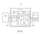
如示於圖1,半導體製造裝置系統100,包含處理裝置(PPE)101、診斷裝置(DIE)111及伺服器(SRV)117。處理裝置(PPE)101,是為了製造半導體裝置而使用的半導體製造裝置,例如為電漿蝕刻裝置等的電漿處理裝置。半導體製造裝置系統100,亦可另稱為半導體裝置製造系統。於以下的說明,有時將處理裝置(PPE)101另稱為半導體製造裝置101。As shown in FIG. 1 , a semiconductor
處理裝置101與診斷裝置111之間,透過LAN佈線(LAN電纜)、USB佈線(USB電纜)或無線LAN等的訊號的發送用及接收用的第1網路線路NWL1進行連接。此外,診斷裝置111與伺服器117之間,透過LAN佈線(LAN電纜)、USB佈線(USB電纜)或無線LAN等的訊號的發送用及接收用的第2網路線路NWL2進行連接。The
處理裝置101,包含處理室(PRR)102、搬送室(COR)103、排氣配管(EPI)104、第1排氣裝置(EXP1)105、第2排氣裝置(EXP2)106、監控排氣配管104的壓力用的第1壓力計(PPM)107、監控搬送室103的壓力用的第2壓力計(CPM)108、閥(VAL)109。The
診斷裝置111,由個人電腦等的電腦構成,包含外部介面電路(EXIF)112、處理器(PROC)113、記憶體(MEM)114、儲存器(STG)115。記憶體114,例如由RAM (Random Access Memory)等的可高速讀取或高速寫入的半導體記憶體而構成。儲存器115,例如由HDD(Hard Disk Drive)、SSD(Solid State Drive)等的大容量的記憶裝置而構成。The
外部介面電路112,在此例,與處理裝置101以網路線路NWL1進行電連接。此外,外部介面電路112,在此例,與伺服器117以網路線路NWL2進行電連接。In this example, the
診斷裝置111,例如透過資料傳輸(DTR)110將搭載於處理裝置101的各種感測器的訊號資料(感測器資料)從外部介面電路112經由網路線路NWL1接收。診斷裝置111,例如將診斷結果等的輸出結果(ORE)116從外部介面電路112經由網路線路NWL2往伺服器117發送。The
伺服器117,在此例,具有將輸出結果116透過GUI118而顯示的顯示部。In this example, the
如示於圖2,為半導體製造裝置的處理裝置(PPE)101,具有:處理為半導體晶圓的樣品212的處理室102;將樣品212往處理室102搬送且連接於處理室102的搬送室103;配置於處理室102與搬送室103之間的閥109。此外,處理裝置101,具有:連接於處理室102的排氣配管104;設於排氣配管104,將處理室102進行排氣的第1排氣裝置105及第2排氣裝置106;計測(監控)排氣配管104的壓力的第1壓力計107;以及計測(監控)搬送室103的壓力的第2壓力計108。As shown in FIG. 2 , a processing device (PPE) 101 of a semiconductor manufacturing device includes: a
處理室102,具有:載置樣品212的作為樣品台的晶圓台210;以及支撐晶圓台210的載台底座211。樣品212,載置於晶圓台210,處理室102的內部被設為既定的狀態(壓力、氣體等),對樣品212實施期望的處理。期望的處理,例如為成膜處理、蝕刻處理、離子植入處理、氧化處理等。The
搬送室103,為樣品212的暫時性的待機場所,在樣品212的往處理室102的搬入之時及樣品212的從處理室102的搬出之時,暫時地收納樣品212。對樣品212實施期望的處理時,樣品212被從搬送室103往處理室102搬入(搬送)。樣品212被往處理室102搬入時,將處理室102與搬送室103之間進行遮斷的閥109開放,處理室102與搬送室103連通。並且,配置於搬送室103內的樣品212,載置於晶圓台210之上。之後,閥109關閉,處理室102與搬送室103之間被遮斷,處理室102成為密封狀態。並且,處理室102內被設為期望的狀態,對樣品212實施期望的處理。另一方面,對樣品212實施期望的處理後,樣品212被從處理室102搬出。將樣品212從處理室102往搬送室103搬出(搬送)時,閥109開放,處理室102與搬送室103連通。並且,載置於晶圓台210之上的樣品212被搬出至搬送室103。之後,閥109關閉,處理室102與搬送室103之間被遮斷。於圖2,以箭頭215示意地示出閥109的開閉的方向,閥109之往上方向的移動,表示閥109開放,閥109的往下方向的移動,表示閥109關閉。閥109開放的狀態,指從搬送室103往處理室102搬送樣品212的情況或從處理室102往搬送室103搬送樣品212的情況。The
第1排氣裝置105,例如採用渦輪分子泵等的真空泵。第2排氣裝置106,例如採用乾式泵等的真空泵。連接於排氣配管104的處理室102,透過第2排氣裝置106粗略地排氣至既定的真空度,之後透過第1排氣裝置105高精度地排氣至既定的高真空。高真空,例如為可進行電漿的產生的真空度。The
第1壓力計107,連接於排氣配管104,可計測(監控)排氣配管104的壓力。據此,可計測(監控)連接於排氣配管104的處理室102的壓力。透過第1壓力計107進行了計測的壓力值(排氣配管104的壓力值),被往診斷裝置111進行資料傳輸110。The
第2壓力計108,連接於搬送室103,可計測(監控)搬送室103的壓力。透過第2壓力計108進行了計測的壓力值(搬送室103的壓力值),被往診斷裝置111進行資料傳輸110。The
如示於圖3,由電腦構成的診斷裝置111被構成為,處理器113例如執行儲存於儲存器115的實現診斷裝置111的功能的軟體程式(亦稱為應用程式),從而透過電腦實現。診斷裝置111具有資料收集部(DAC)303以及診斷部(DIG)305。於診斷裝置111,各功能(303、305)亦可由硬體電路構成。As shown in FIG3 , the
資料收集部(DAC)303具備一功能,該功能為,接收透過資料傳輸110發送的壓力值(排氣配管104的壓力值PE(處理室102的壓力值)與搬送室103的壓力值PT)的資料,作為裝置資料(DED)304而保存於儲存器115。The data collection unit (DAC) 303 has a function of receiving data of pressure values (pressure value PE of the exhaust pipe 104 (pressure value of the processing chamber 102) and pressure value PT of the transfer chamber 103) sent through the
診斷部(DIG)305具有處理部(PRC)306、閾值資料(DTH)307以及相關計算用資料(DCC)308。處理部(PRC)306,被透過由處理器113執行軟體程式從而實現。閾值資料(DTH)307及相關計算用資料(DCC)308,保存於儲存器115。The diagnosis unit (DIG) 305 includes a processing unit (PRC) 306, threshold data (DTH) 307, and correlation calculation data (DCC) 308. The processing unit (PRC) 306 is implemented by the
相關計算用資料(DCC)308,由在閥109開放後的既定期間中的排氣配管104的壓力值PE及搬送室103的壓力值PT的過去的歷史資料構成。此過去的歷史資料,例如可從裝置資料(DED)304獲得。閥109開放後的既定期間,不特別限制,惟例如可設為在閥109成為開狀態後5秒至10秒(5秒~10秒)之時間範圍。此處,異常檢測方法方面,雖以壓力的最大值進行說明,惟其他變數(參數)亦無問題,具體而言,舉第1排氣裝置105的電流的統計量等作為異常檢測的候補。The relevant calculation data (DCC) 308 is composed of the past historical data of the pressure value PE of the
處理部(PRC)306,基於相關計算用資料(DCC)308而繪製(作成)圖形。並且,處理部(PRC)306,基於作成的圖形,生成表示搬送室103的壓力值與排氣配管104的最大壓力值之間的相關的回歸曲線(排氣配管104的壓力值=f(P(搬送室103的壓力值)))。並且,處理部(PRC)306,選擇排氣配管104的最大壓力值之上位既定數(例如,前10個最大壓力值),計算選擇的前10個最大壓力值的平均值(PEVA10)。處理部(PRC)306,基於選擇的前10個最大壓力值的平均值(PEVA10),生成排氣配管104的壓力值PE的閾值PETH。閾值PETH,例如可設為平均值(PEVA10)的85%至95%之間的壓力值,較優選上可設為90%左右的壓力值。處理部(PRC)306,此外將閾值PETH代入於回歸曲線(排氣配管104的壓力值=f(P(搬送室103的壓力值))),從而生成搬送室103的壓力值的閾值(亦稱為既定值)PTTH。亦即,基於在閥109開放後的既定期間中的為排氣裝置(105、106)之壓力的最大值與搬送室103的壓力的相關之回歸曲線,求出既定值(閾值PTTH)。閾值PETH、PTTH,被作為閾值資料(DTH)307保存於儲存器115。閾值PETH、PTTH方面,於後述的圖7及圖11詳細進行說明。The processing unit (PRC) 306 draws (creates) a graph based on the relevant calculation data (DCC) 308. Furthermore, the processing unit (PRC) 306 generates a regression curve representing the correlation between the pressure value of the
於圖4,示出圖3的裝置資料(DED)304、閾值資料(DTH)307及相關計算用資料(DCC)308的資料構成的一例。FIG. 4 shows an example of the data structure of the device data (DED) 304, the threshold data (DTH) 307, and the correlation calculation data (DCC) 308 of FIG. 3.
裝置資料(DED)304,為由第1壓力計107與第2壓力計108計測的排氣配管104的壓力值PE與搬送室103的壓力值PT之時序列資料,包含年月日(Date)、時間(Time)、閥開判定(VALOJ)、排氣配管104的壓力值PE以及搬送室103的壓力值PT。閥開判定(VALOJ),表示閥109的開狀態(OPEN)與閉狀態(CLOSE)的判定結果。The device data (DED) 304 is time series data of the pressure value PE of the
閾值資料(DTH)307,包含排氣配管104的壓力值PE的閾值PETH以及搬送室103的壓力值PT的閾值PTTH。The threshold data (DTH) 307 includes a threshold value PETH of the pressure value PE of the
相關計算用資料(DCC)308,包含複數組的排氣配管104的壓力值PE與搬送室103的壓力值PT。The correlation calculation data (DCC) 308 includes a plurality of sets of pressure values PE of the
診斷裝置111,由個人電腦構成,具備一平台,該平台實現了檢測半導體製造裝置101的排氣裝置(第1排氣裝置105、第2排氣裝置106)或排氣配管104的異常用的應用程式。診斷裝置111,透過網路連接於半導體製造裝置101,該半導體製造裝置101具有處理樣品212的處理室102、為了將樣品212往處理室102搬送而連接於處理室102的搬送室103、將處理室102與搬送室103之間進行遮斷的閥109、連接於處理室102的排氣裝置(105、106)與排氣配管104以及計測(監控)排氣配管104的壓力的第1壓力計107。診斷裝置111,使用透過壓力計107進行了計測的閥109開放後的既定期間的壓力值,判定半導體製造裝置101的排氣裝置(105、106)或排氣配管104的異常有無。亦即,基於閥109開放後的排氣裝置(105、106)之壓力,透過診斷裝置111判定排氣裝置(105、106)或排氣裝置(105、106)之排氣配管104的異常有無。The
此處,針對本揭示的診斷裝置111的異常有無的判定的動作流程進行說明。Here, the operation flow of determining whether or not there is an abnormality in the
診斷裝置111,使用在閥109開放後的既定期間,例如使用5秒至10秒的範圍的既定期間的排氣配管104的壓力值,判定半導體製造裝置101的排氣裝置(105、106)或排氣配管104的異常有無。將閥109開放後的既定期間的排氣配管104的壓力值利用於異常有無的判定,故可不需要考量處理室102中的處理條件的變異性導致的排氣配管104的壓力值的變動。據此,變得可抑制排氣配管104的壓力值的變動,可正確地判定半導體製造裝置101的排氣裝置(105、106)或排氣配管104的異常有無。The
此外,依本揭示者的見解時,透過第1壓力計107與第2壓力計108而計測之處的排氣配管104的壓力值PE與搬送室103的壓力值PT,具有既定的相關關係。另一方面,透過第1壓力計107而計測的排氣配管104的壓力值,有時即使在閥109開放後,仍會在計測的壓力值方面產生變異性(雜訊)。於是,得知為了排除所計測的排氣配管104的壓力值的變異性,優選上導入利用於排氣配管104的壓力值PE的判定的閾值(PETH)。此外,同樣的見解亦可見於第1排氣裝置105的電流值的最大值。另外,閾值(PETH)的計算方面,可參照後述的圖7及圖11的說明。Furthermore, according to the opinion of the present discloser, the pressure value PE of the
診斷裝置111,在第2壓力計108的壓力值在閥109開放後的既定期間超過為既定的閾值(既定值)的閾值PTTH的情況(第2壓力計108的壓力值>PTTH)下,判定為半導體製造裝置101的排氣裝置105、106或排氣配管104為異常。亦即,閥109開放後的搬送室103的壓力成為既定值以上的情況下,透過診斷裝置111判定異常有無。據此,可在抑制對於半導體製造裝置101的樣品之處理條件導致的排氣配管104的壓力值的變異性以及在閥109開放後的既定期間所計測的排氣配管104的壓力值的變異性(雜訊)之下,正確地判定半導體製造裝置101的排氣裝置105、106或排氣配管104的異常。The
在以上的說明,雖說明了設有透過網路連接於半導體製造裝置101的診斷裝置111的半導體製造裝置系統100的構成例,惟診斷裝置111不限定於此構成例。診斷裝置111,例如亦可由在伺服器SRV執行的軟體而構成,將該伺服器SRV透過網路連接於半導體製造裝置101從而構成。In the above description, although the configuration example of the semiconductor
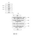
接著,使用圖5,說明診斷裝置111實施的診斷演算法之異常診斷流程。圖5,為實施例之診斷裝置的處理流程圖。此診斷方法之處理流程,表示診斷演算法之異常診斷流程。於圖5,示出包含半導體製造裝置101的動作流程50以及診斷裝置111的異常診斷的動作流程51的診斷方法。Next, the abnormality diagnosis process of the diagnostic algorithm implemented by the
首先,說明半導體製造裝置101的動作流程50。First, the
半導體製造裝置101的動作流程50,具有步驟S100、步驟S101以及步驟S102。The operation flow 50 of the
步驟S100:從閥109關閉的狀態(Close)設為開放的狀態(Open)。Step S100: Change the
步驟S101:在閥109開放的狀態下,將為處理前的樣品212之晶圓從搬送室103往處理室102的內部搬入。或者,將為處理後的樣品212之晶圓從處理室102往搬送室103的內部搬出。Step S101: With the
步驟S102:從閥109開放的狀態(Open)設為關閉的狀態(Close)。另外,從步驟S100至步驟S102中,第1壓力計107與第2壓力計108,計測排氣配管104的壓力值PE與搬送室103的壓力值PT,往診斷裝置111的資料收集部(DAC)303進行資料傳輸110,於裝置資料(DED)304,儲存有時序列資料。Step S102: Set the
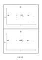
圖8,為實施例之半導體製造裝置101的排氣配管104的壓力值PE與搬送室103的壓力值PT的構成例的說明圖。於圖8,圖形81,橫軸表示時間T,縱軸表示由第1壓力計107計測的排氣配管104的壓力值PE。圖形82,橫軸表示時間T,縱軸表示由第2壓力計108計測的搬送室103的壓力值PT。83表示閥109開放的狀態(Open)的期間。TA表示閥109開放的狀態(Open)後的既定期間。既定期間TA,例如為5秒至10秒的範圍。使用在閥109開放的狀態(Open)後的既定期間TA之排氣配管104的壓力值PE,判定半導體製造裝置101的排氣裝置(105、106)或排氣配管104的異常有無。FIG8 is an explanatory diagram of a configuration example of the pressure value PE of the
如示於圖5,診斷裝置111的動作流程51,具有步驟S200、步驟S201、步驟S202以及步驟S203。As shown in FIG. 5 , the
步驟S200:診斷裝置111的處理部306,從資料收集部(DAC)303,針對處理室102的排氣配管104的壓力值PE與搬送室103的壓力值PT,取得閥109開放的狀態(Open)後之時序列資料(圖8參照)。Step S200: The processing
步驟S201:診斷裝置111的處理部306,於取得的時序列資料,算出閥109開放的狀態(Open)後的既定期間TA內的處理室102的排氣配管104的壓力值PE。Step S201: The processing
步驟S202:處理部306,將在步驟S201算出的排氣配管104的壓力值PE代入於結果壓力。Step S202: The processing
步驟S203:處理部306在結果壓力比排氣配管104的壓力值PE的閾值PETH大的情況(排氣配管104的壓力值PE>PETH)下,進行異常報送。另一方面,結果壓力不比閾值PETH大的情況(排氣配管104的壓力值PE<PETH)下,不進行異常報送,結束異常診斷的動作流程。此處,排氣配管104的壓力值PE的閾值PETH,可參照後述的圖7及圖11的說明。Step S203: When the result pressure is greater than the threshold value PETH of the pressure value PE of the exhaust pipe 104 (the pressure value PE of the
亦即,基於閥109開放後的排氣裝置(105、106)之壓力而判定排氣裝置(105、106)或排氣裝置(105、106)之排氣配管104的異常有無的步驟(S200-S203),被透過診斷半導體製造裝置101的狀態用的應用程式而執行。That is, the steps (S200-S203) of determining whether there is an abnormality in the exhaust device (105, 106) or the
圖9,為排氣配管104的壓力值PE(處理中與閥開後)的說明圖。圖9中,圖形91為正在將樣品212在處理室102內進行處理中的排氣配管104的壓力值PE的一例,橫軸表示時間T,縱軸表示排氣配管104的壓力值PE。圖形92,為閥109開放的狀態(Open)後的既定期間TA的排氣配管104的壓力值PE的一例,橫軸表示時間T,縱軸表示排氣配管104的壓力值PE。FIG9 is an explanatory diagram of the pressure value PE of the exhaust pipe 104 (during processing and after the valve is opened). In FIG9, FIG91 is an example of the pressure value PE of the
如示於圖形91,正在將樣品212在處理室102內進行處理中的排氣配管104的壓力值PE,可得知依處理條件,成為高的壓力值或成為低的壓力值,具有變異性。As shown in FIG. 91 , the pressure value PE of the
另一方面,如示於圖形92,在閥109開放的狀態(Open)後的既定期間TA的排氣配管104的壓力值PE,可得知比起示於圖形91的排氣配管104的壓力值PE,壓力值PE的變異性被抑制。亦即,在檢測半導體製造裝置101的排氣裝置105、106或排氣配管104的異常之際,基於閥109開放的狀態(Open)後的既定期間TA的排氣配管104的壓力值PE而檢測異常,使得可在抑制處理條件導致的壓力值PE的變異性之下,檢測半導體製造裝置101的排氣裝置105、106或排氣配管104的異常。On the other hand, as shown in FIG92, the pressure value PE of the
在圖形92,可得知雖抑制了處理條件導致的壓力值PE的變異性,惟在壓力值PE的一部分,產生不少的變異性(雜訊)。於是,設定排氣配管104的壓力值PE的閾值PETH,依排氣配管104的壓力值PE是否比閾值PETH大,從而判斷是否進行通知在導體製造裝置101的排氣裝置105、106或排氣配管104存在異常的異常報送為佳。據此,可在抑制在閥109開放後的既定期間所計測的排氣配管104的壓力值的變異性(雜訊)之下,正確地判定半導體製造裝置101的排氣裝置105、106或排氣配管104的異常。In Fig. 92, it can be seen that although the variability of the pressure value PE caused by the processing conditions is suppressed, a considerable variability (noise) is generated in a part of the pressure value PE. Therefore, a threshold value PETH of the pressure value PE of the
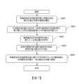
接著,使用圖6,說明關於診斷裝置111實施的診斷演算法之異常診斷流程的別例。圖6,為實施例之診斷裝置的別的處理流程圖。此處理流程,表示診斷演算法之異常診斷流程。於圖6,示出包含半導體製造裝置101的動作流程50以及診斷裝置111的異常診斷的動作流程61的診斷方法。Next, another example of the abnormality diagnosis process of the diagnostic algorithm implemented by the
半導體製造裝置101的動作流程50,與圖5的半導體製造裝置101的動作流程50相同,故重複之說明省略。The operation flow 50 of the
診斷裝置111的異常診斷的動作流程61,具有步驟S200、步驟S301、步驟S302、步驟S303、步驟S304及步驟S203。The abnormality
步驟S200:診斷裝置111的處理部306,從資料收集部(DAC)303,針對處理室102的排氣配管104的壓力值PE與搬送室103的壓力值PT,取得閥109開放的狀態(Open)後之時序列資料(圖8參照)。Step S200: The processing
步驟S301:診斷裝置111的處理部306,於取得的時序列資料,算出(抽出)閥109開放的狀態(Open)後的既定期間TA內的處理室102的排氣配管104的最大壓力值PE。Step S301: The processing
步驟S302:診斷裝置111的處理部306,判定在閥109開放的狀態(Open)後的既定期間TA內的搬送室103的壓力值PT,是否為搬送室103的壓力值PT的閾值PTTH以上。在既定期間TA內的搬送室103的壓力值PT為閾值PTTH以上(PT>PTTH)的情況(是)下,移至步驟S303。在既定期間TA內的搬送室103的壓力值PT非閾值PTTH以上(PT>PTTH)的情況(否)下,移至步驟S304。Step S302: The processing
步驟S303:處理部306,將在步驟S201算出的排氣配管104的最大壓力值代入於結果壓力。Step S303: The processing
步驟S304:處理部306,使結果壓力無效,結束異常診斷的動作流程。Step S304:
步驟S203:處理部306在結果壓力比排氣配管104的壓力值PE的閾值PETH大的情況(排氣配管104的壓力值PE>PETH)下,進行異常報送。另一方面,結果壓力不比閾值PETH大的情況(排氣配管104的壓力值PE<PETH)下,不進行異常報送,結束異常診斷的動作流程。Step S203: The processing
亦即,基於閥109開放後的排氣裝置(105、106)之壓力而判定排氣裝置(105、106)或排氣裝置(105、106)之排氣配管104的異常有無的步驟(S200、S301-S304、S203),被透過診斷半導體製造裝置101的狀態用的應用程式而執行。That is, the steps (S200, S301-S304, S203) of determining whether there is an abnormality in the exhaust device (105, 106) or the
接著,利用圖7、圖10及圖11,針對排氣配管104的壓力值PE的閾值PETH及搬送室103的壓力值PT的閾值PTTH進行說明。圖7,為決定實施例之排氣配管104的壓力閾值(PETH)與搬送室103的壓力閾值(PTTH)用的處理流程圖。圖10,為搬送室103的壓力值PT(閾值應用前與閾值應用後)的說明圖。圖11,為從排氣配管104的壓力值PE與搬送室103的壓力值PT的相關計算用資料(DCC)決定排氣配管104的壓力值PE的閾值PETH及搬送室103的壓力值PT的閾值PTTH之一例的說明圖。Next, the threshold value PETH of the pressure value PE of the
於圖7,示出處理部306決定搬送室103的壓力值PT的閾值PTTH用的處理流程;此處理流程,於任意之時序,被透過處理部306執行。處理流程,具有步驟S400、步驟S401、步驟S402、步驟S403以及步驟S404。7 shows a process flow for the
步驟S400:處理部(PRC)306,基於相關計算用資料(DCC)308而繪製(作成)圖形。相關計算用資料(DCC)308,由在閥109開放後的既定期間中的排氣配管104的壓力值PE及搬送室103的壓力值PT的過去的歷史資料構成。此過去的歷史資料,例如可從裝置資料(DED)304獲得。閥109開放後的既定期間,不特別限制,惟例如可設為在閥109成為開狀態後5秒至10秒(5秒~10秒)之時間範圍。Step S400: The processing unit (PRC) 306 draws (creates) a graph based on the relevant calculation data (DCC) 308. The relevant calculation data (DCC) 308 is composed of the past history data of the pressure value PE of the
步驟S401:處理部(PRC)306,基於作成的圖形,生成搬送室103的壓力值PT與排氣配管104的最大壓力值之間的回歸曲線RC(圖11參照)。亦即,此處,排氣配管104的壓力值PE與搬送室103的壓力值PT具有既定的相關關係,故作成搬送室103的壓力值PT與欲判定異常的處理室102的排氣配管104的壓力值PE的最大壓力值之間的回歸曲線RC。回歸曲線RC,例如利用以下的式子表示。Step S401: The processing unit (PRC) 306 generates a regression curve RC between the pressure value PT of the
排氣配管104的壓力值PE=f(P(搬送室103的壓力值PT)) 步驟S402:處理部(PRC)306,選擇排氣配管104的最大壓力值之上位既定數(例如,前10個最大壓力值)(圖11參照)。The pressure value PE of the
步驟S403:計算選擇的前10個最大壓力值的平均值(PEVA10)(圖11參照)。Step S403: Calculate the average value (PEVA10) of the first 10 selected maximum pressure values (see FIG. 11 ).
步驟S404:處理部(PRC)306,基於選擇的前10個最大壓力值的平均值(PEVA10),生成排氣配管104的壓力值PE的閾值PETH。閾值PETH,例如可設為平均值(PEVA10)的85%至95%之間的壓力值,較優選上可設為平均值(PEVA10)的90%左右的壓力值。處理部(PRC)306,此外將閾值PETH代入於回歸曲線RC,從而生成搬送室103的壓力值PT的閾值PTTH。閾值PETH、PTTH,透過處理部(PRC)306,被作為閾值資料(DTH)307而保存於儲存器115。Step S404: The processing unit (PRC) 306 generates a threshold value PETH of the pressure value PE of the
設定以圖7求出的搬送室103的壓力值PT的閾值PTTH,從而可抑制示於圖10的圖形92(與圖9的圖形92相同)的變異性(雜訊)。圖10的圖形93,為在應用了搬送室103的壓力值PT的閾值PTTH的情況下的閥109開放的狀態(Open)後的既定期間TA的排氣配管104的壓力值PE的一例,橫軸表示時間T,縱軸表示排氣配管104的壓力值PE。亦即,可得知由於應用閾值PTTH,使得抑制了閥109開放的狀態(Open)後的既定期間TA的排氣配管104的壓力值PE的變異性。By setting the threshold PTTH of the pressure value PT of the
亦即,使用閥109開放後的既定期間TA的排氣配管104的壓力值PE,從而可抑制處理條件導致的變異性(參照圖9的圖形91與圖形92)。此外,於搬送室103的壓力值PT設定閾值(PTTH),使得變異性從存在處理條件導致的變異性的狀態(圖9的圖形91參照)改善71%左右(圖10的圖形93參照)。此處,雖以壓力值進行了說明,惟使用第1排氣裝置105的電流值的統計量,亦獲得同樣的效果。That is, by using the pressure value PE of the
依實施例之診斷裝置時,可在抑制處理條件導致的變異性之下,判定半導體製造裝置的排氣裝置或排氣配管的異常有無。According to the diagnostic device of the embodiment, it is possible to determine whether there is an abnormality in the exhaust device or exhaust piping of the semiconductor manufacturing device while suppressing the variability caused by the processing conditions.
以上,基於實施例具體說明了本發明人創作的發明;然而,本發明,當然不限定於上述實施方式及實施例,可作各種變更。The invention created by the inventor is described above in detail based on the embodiments; however, the invention is certainly not limited to the above-mentioned implementation methods and embodiments, and various modifications can be made.
100:半導體製造裝置系統 101:半導體製造裝置(處理裝置) 102:處理室 103:搬送室 104:排氣配管 105:第1排氣裝置 106:第2排氣裝置 107:第1壓力計 108:第2壓力計 109:閥 111:診斷裝置 117:伺服器 210:晶圓台 212:樣品100: Semiconductor manufacturing equipment system101: Semiconductor manufacturing equipment (processing equipment)102: Processing room103: Transfer room104: Exhaust pipe105: First exhaust device106: Second exhaust device107: First pressure gauge108: Second pressure gauge109: Valve111: Diagnostic equipment117: Server210: Wafer stage212: Sample
[圖1]圖1為實施例之半導體製造裝置系統的硬體構成圖。 [圖2]圖2為圖1的處理裝置的硬體構成圖。 [圖3]圖3為圖1的診斷裝置的功能塊的說明圖。 [圖4]圖4為說明圖3的裝置資料、閾值資料及相關計算用資料的資料構成例的圖。 [圖5]圖5為實施例之診斷裝置的處理流程圖。 [圖6]圖6為實施例之診斷裝置的其他處理流程圖。 [圖7]圖7為決定實施例之排氣配管的壓力閾值與搬送室的壓力閾值用的處理流程圖。 [圖8]圖8為實施例之半導體製造裝置的排氣配管的壓力與搬送室的壓力的構成例的說明圖。 [圖9]圖9為排氣配管的壓力(處理中與閥開後)的說明圖。 [圖10]圖10為搬送室的壓力(閾值應用前與閾值應用後)的說明圖。 [圖11]圖11為從排氣配管的壓力與搬送室的壓力決定排氣配管的壓力的閾值及搬送室的壓力的閾值之例的說明圖。[Figure 1] Figure 1 is a hardware configuration diagram of a semiconductor manufacturing device system of an embodiment.[Figure 2] Figure 2 is a hardware configuration diagram of a processing device of Figure 1.[Figure 3] Figure 3 is an explanatory diagram of a functional block of a diagnostic device of Figure 1.[Figure 4] Figure 4 is a diagram illustrating an example of a data configuration of device data, threshold data, and related calculation data of Figure 3.[Figure 5] Figure 5 is a processing flow chart of a diagnostic device of an embodiment.[Figure 6] Figure 6 is another processing flow chart of a diagnostic device of an embodiment.[Figure 7] Figure 7 is a processing flow chart for determining a pressure threshold of an exhaust pipe and a pressure threshold of a transfer chamber of an embodiment.[Figure 8] Figure 8 is an explanatory diagram of an example of the configuration of the pressure of the exhaust pipe and the pressure of the transfer chamber of the semiconductor manufacturing device of the embodiment.[Figure 9] Figure 9 is an explanatory diagram of the pressure of the exhaust pipe (during processing and after the valve is opened).[Figure 10] Figure 10 is an explanatory diagram of the pressure of the transfer chamber (before and after the threshold is applied).[Figure 11] Figure 11 is an explanatory diagram of an example of determining the threshold of the pressure of the exhaust pipe and the threshold of the pressure of the transfer chamber from the pressure of the exhaust pipe and the pressure of the transfer chamber.
Claims (5)
Translated fromChineseApplications Claiming Priority (2)
| Application Number | Priority Date | Filing Date | Title |
|---|---|---|---|
| WOPCT/JP2022/013658 | 2022-03-23 | ||
| PCT/JP2022/013658WO2023181208A1 (en) | 2022-03-23 | 2022-03-23 | Diagnostic device, semiconductor manufacturing apparatus system, semiconductor device manufacturing system, and diagnostic method |
Publications (2)
| Publication Number | Publication Date |
|---|---|
| TW202338541A TW202338541A (en) | 2023-10-01 |
| TWI878805Btrue TWI878805B (en) | 2025-04-01 |
Family
ID=88100556
Family Applications (1)
| Application Number | Title | Priority Date | Filing Date |
|---|---|---|---|
| TW112106469ATWI878805B (en) | 2022-03-23 | 2023-02-22 | Diagnostic device, semiconductor manufacturing device system, semiconductor device manufacturing system and diagnostic method |
Country Status (6)
| Country | Link |
|---|---|
| US (1) | US20250014923A1 (en) |
| JP (2) | JP7496932B2 (en) |
| KR (1) | KR20230140546A (en) |
| CN (1) | CN117121157A (en) |
| TW (1) | TWI878805B (en) |
| WO (1) | WO2023181208A1 (en) |
Citations (10)
| Publication number | Priority date | Publication date | Assignee | Title |
|---|---|---|---|---|
| TW200641981A (en)* | 2005-05-17 | 2006-12-01 | Hitachi High Tech Corp | Plasma processing apparatus |
| TW200725686A (en)* | 2005-10-03 | 2007-07-01 | Advanced Tech Materials | Systems and methods for determination of endpoint of chamber cleaning processes |
| JP2008072030A (en)* | 2006-09-15 | 2008-03-27 | Matsushita Electric Ind Co Ltd | Plasma processing apparatus, abnormality detection method of plasma processing apparatus, and plasma processing method |
| JP2010027836A (en)* | 2008-07-18 | 2010-02-04 | Panasonic Corp | Plasma treatment apparatus |
| TWI407498B (en)* | 2008-09-30 | 2013-09-01 | Mitsubishi Heavy Ind Ltd | A wafer bonding apparatus and a method of bonding wafers |
| TW201736998A (en)* | 2016-03-29 | 2017-10-16 | Hitachi Int Electric Inc | Processing device, device management controller, and recording medium |
| TW201933510A (en)* | 2017-11-08 | 2019-08-16 | 日商東京威力科創股份有限公司 | Gas supply system and gas supply method |
| US20200023487A1 (en)* | 2017-03-31 | 2020-01-23 | Ebara Corporation | Substrate processing apparatus |
| US20200081423A1 (en)* | 2018-03-20 | 2020-03-12 | Tokyo Electron Limited | Self-aware and correcting heterogenous platform incorporating integrated semiconductor processing modules and method for using same |
| JP2021012654A (en)* | 2019-07-09 | 2021-02-04 | 東京エレクトロン株式会社 | Board processing system and process data monitoring method |
Family Cites Families (9)
| Publication number | Priority date | Publication date | Assignee | Title |
|---|---|---|---|---|
| JP4387573B2 (en)* | 1999-10-26 | 2009-12-16 | 東京エレクトロン株式会社 | Process exhaust gas monitoring apparatus and method, semiconductor manufacturing apparatus, and semiconductor manufacturing apparatus management system and method |
| US7122096B2 (en)* | 2003-03-04 | 2006-10-17 | Hitachi High-Technologies Corporation | Method and apparatus for processing semiconductor |
| KR101208295B1 (en)* | 2004-12-28 | 2012-12-05 | 도쿄엘렉트론가부시키가이샤 | Semiconductor manufacturing apparatus, method for detecting abnormality in such semiconductor manufacturing apparatus, and recording medium wherein computer program for executing such method is recorded |
| US7438534B2 (en)* | 2005-10-07 | 2008-10-21 | Edwards Vacuum, Inc. | Wide range pressure control using turbo pump |
| JP2007186757A (en) | 2006-01-13 | 2007-07-26 | Tokyo Electron Ltd | Vacuum treatment apparatus and vacuum treatment method |
| JP4688764B2 (en) | 2006-09-19 | 2011-05-25 | 東京エレクトロン株式会社 | Substrate removal method for substrate processing apparatus |
| JP6613276B2 (en) | 2017-09-22 | 2019-11-27 | 株式会社Kokusai Electric | Semiconductor device manufacturing method, program, recording medium, and substrate processing apparatus |
| US11133204B2 (en)* | 2019-01-29 | 2021-09-28 | Applied Materials, Inc. | Chamber matching with neural networks in semiconductor equipment tools |
| JP7467261B2 (en) | 2020-06-30 | 2024-04-15 | 東京エレクトロン株式会社 | Anomaly detection device, semiconductor manufacturing device, and anomaly detection method |
- 2022
- 2022-03-23KRKR1020237004558Apatent/KR20230140546A/enactivePending
- 2022-03-23CNCN202280005991.5Apatent/CN117121157A/enactivePending
- 2022-03-23WOPCT/JP2022/013658patent/WO2023181208A1/ennot_activeCeased
- 2022-03-23JPJP2023512205Apatent/JP7496932B2/enactiveActive
- 2022-03-23USUS18/026,079patent/US20250014923A1/enactivePending
- 2023
- 2023-02-22TWTW112106469Apatent/TWI878805B/enactive
- 2024
- 2024-05-28JPJP2024085969Apatent/JP7662878B2/enactiveActive
Patent Citations (10)
| Publication number | Priority date | Publication date | Assignee | Title |
|---|---|---|---|---|
| TW200641981A (en)* | 2005-05-17 | 2006-12-01 | Hitachi High Tech Corp | Plasma processing apparatus |
| TW200725686A (en)* | 2005-10-03 | 2007-07-01 | Advanced Tech Materials | Systems and methods for determination of endpoint of chamber cleaning processes |
| JP2008072030A (en)* | 2006-09-15 | 2008-03-27 | Matsushita Electric Ind Co Ltd | Plasma processing apparatus, abnormality detection method of plasma processing apparatus, and plasma processing method |
| JP2010027836A (en)* | 2008-07-18 | 2010-02-04 | Panasonic Corp | Plasma treatment apparatus |
| TWI407498B (en)* | 2008-09-30 | 2013-09-01 | Mitsubishi Heavy Ind Ltd | A wafer bonding apparatus and a method of bonding wafers |
| TW201736998A (en)* | 2016-03-29 | 2017-10-16 | Hitachi Int Electric Inc | Processing device, device management controller, and recording medium |
| US20200023487A1 (en)* | 2017-03-31 | 2020-01-23 | Ebara Corporation | Substrate processing apparatus |
| TW201933510A (en)* | 2017-11-08 | 2019-08-16 | 日商東京威力科創股份有限公司 | Gas supply system and gas supply method |
| US20200081423A1 (en)* | 2018-03-20 | 2020-03-12 | Tokyo Electron Limited | Self-aware and correcting heterogenous platform incorporating integrated semiconductor processing modules and method for using same |
| JP2021012654A (en)* | 2019-07-09 | 2021-02-04 | 東京エレクトロン株式会社 | Board processing system and process data monitoring method |
Also Published As
| Publication number | Publication date |
|---|---|
| JP7662878B2 (en) | 2025-04-15 |
| TW202338541A (en) | 2023-10-01 |
| JP2024109877A (en) | 2024-08-14 |
| WO2023181208A1 (en) | 2023-09-28 |
| US20250014923A1 (en) | 2025-01-09 |
| KR20230140546A (en) | 2023-10-06 |
| CN117121157A (en) | 2023-11-24 |
| JP7496932B2 (en) | 2024-06-07 |
| JPWO2023181208A1 (en) | 2023-09-28 |
Similar Documents
| Publication | Publication Date | Title |
|---|---|---|
| CN113330463B (en) | Using Neural Networks for Chamber Matching in Semiconductor Equipment Tools | |
| US6706543B2 (en) | Method of monitoring and/or controlling a semiconductor manufacturing apparatus and a therefor | |
| US8751196B2 (en) | Abnormality detection system, abnormality detection method, recording medium, and substrate processing apparatus | |
| CN104238543B (en) | The bad pattern method of inspection and its device of the sensing data of time series form | |
| JPWO2020136823A1 (en) | Abnormality diagnosis device and abnormality diagnosis method | |
| KR20210017651A (en) | Method for Fault Detection and Fault Diagnosis in Semiconductor Manufacturing Process | |
| TWI878805B (en) | Diagnostic device, semiconductor manufacturing device system, semiconductor device manufacturing system and diagnostic method | |
| KR20230104951A (en) | Substrate processing system tools to monitor, evaluate and respond based on health, including sensor mapping and triggered datalogging | |
| JP2016134585A (en) | Semiconductor manufacturing device, diagnosis system for the same, and method of manufacturing semiconductor device | |
| JP2006146459A (en) | Method and system for manufacturing semiconductor device | |
| CN114203588A (en) | Chamber leak detection method and semiconductor process equipment | |
| CN112585727B (en) | Device diagnosis device, plasma processing device, and device diagnosis method | |
| US20070043534A1 (en) | System and method for electronic diagnostics of a process vacuum environment | |
| US20060206230A1 (en) | Method and apparatus for detecting abnormal characteristic values capable of suppressing detection of normal characteristic values | |
| CN112997177B (en) | Attack detection device, attack detection method, and attack detection program | |
| JP4836994B2 (en) | Semiconductor processing equipment | |
| CN116933028A (en) | Telemetry data anomaly detection method based on B-spline envelope analysis | |
| CN116756673A (en) | Multi-sensor abnormality detection method, device, computer equipment and storage medium | |
| US20060224267A1 (en) | Method and apparatus for detecting abnormal characteristic values capable of suppressing detection of normal characteristic values | |
| TWI849766B (en) | Diagnostic device, semiconductor manufacturing device system, semiconductor device manufacturing system and diagnostic method | |
| TWI895961B (en) | Abnormality detection device and abnormality detection method | |
| TW202435111A (en) | Abnormality detection device and abnormality detection method | |
| CN120234596B (en) | Peak extraction method, thickness measurement method and equipment | |
| JP2002099328A (en) | Monitoring device, process device, monitoring method, data collection method, and semiconductor device manufacturing method | |
| CN118073248A (en) | Method for detecting etching equipment and method for etching wafer |