TWI878311B - Camera equipment and electronic equipment - Google Patents
Camera equipment and electronic equipmentDownload PDFInfo
- Publication number
- TWI878311B TWI878311BTW109121768ATW109121768ATWI878311BTW I878311 BTWI878311 BTW I878311BTW 109121768 ATW109121768 ATW 109121768ATW 109121768 ATW109121768 ATW 109121768ATW I878311 BTWI878311 BTW I878311B
- Authority
- TW
- Taiwan
- Prior art keywords
- transistor
- circuit
- layer
- wiring
- insulating layer
- Prior art date
Links
Images


Classifications
- H—ELECTRICITY
- H10—SEMICONDUCTOR DEVICES; ELECTRIC SOLID-STATE DEVICES NOT OTHERWISE PROVIDED FOR
- H10F—INORGANIC SEMICONDUCTOR DEVICES SENSITIVE TO INFRARED RADIATION, LIGHT, ELECTROMAGNETIC RADIATION OF SHORTER WAVELENGTH OR CORPUSCULAR RADIATION
- H10F39/00—Integrated devices, or assemblies of multiple devices, comprising at least one element covered by group H10F30/00, e.g. radiation detectors comprising photodiode arrays
- H10F39/80—Constructional details of image sensors
- H10F39/802—Geometry or disposition of elements in pixels, e.g. address-lines or gate electrodes
- H10F39/8023—Disposition of the elements in pixels, e.g. smaller elements in the centre of the imager compared to larger elements at the periphery
- H—ELECTRICITY
- H04—ELECTRIC COMMUNICATION TECHNIQUE
- H04N—PICTORIAL COMMUNICATION, e.g. TELEVISION
- H04N25/00—Circuitry of solid-state image sensors [SSIS]; Control thereof
- H04N25/70—SSIS architectures; Circuits associated therewith
- H—ELECTRICITY
- H04—ELECTRIC COMMUNICATION TECHNIQUE
- H04N—PICTORIAL COMMUNICATION, e.g. TELEVISION
- H04N25/00—Circuitry of solid-state image sensors [SSIS]; Control thereof
- H04N25/70—SSIS architectures; Circuits associated therewith
- H04N25/76—Addressed sensors, e.g. MOS or CMOS sensors
- H04N25/77—Pixel circuitry, e.g. memories, A/D converters, pixel amplifiers, shared circuits or shared components
- H—ELECTRICITY
- H10—SEMICONDUCTOR DEVICES; ELECTRIC SOLID-STATE DEVICES NOT OTHERWISE PROVIDED FOR
- H10B—ELECTRONIC MEMORY DEVICES
- H10B12/00—Dynamic random access memory [DRAM] devices
- H—ELECTRICITY
- H10—SEMICONDUCTOR DEVICES; ELECTRIC SOLID-STATE DEVICES NOT OTHERWISE PROVIDED FOR
- H10D—INORGANIC ELECTRIC SEMICONDUCTOR DEVICES
- H10D30/00—Field-effect transistors [FET]
- H10D30/60—Insulated-gate field-effect transistors [IGFET]
- H10D30/67—Thin-film transistors [TFT]
- H—ELECTRICITY
- H10—SEMICONDUCTOR DEVICES; ELECTRIC SOLID-STATE DEVICES NOT OTHERWISE PROVIDED FOR
- H10D—INORGANIC ELECTRIC SEMICONDUCTOR DEVICES
- H10D84/00—Integrated devices formed in or on semiconductor substrates that comprise only semiconducting layers, e.g. on Si wafers or on GaAs-on-Si wafers
- H10D84/01—Manufacture or treatment
- H10D84/0123—Integrating together multiple components covered by H10D12/00 or H10D30/00, e.g. integrating multiple IGBTs
- H10D84/0126—Integrating together multiple components covered by H10D12/00 or H10D30/00, e.g. integrating multiple IGBTs the components including insulated gates, e.g. IGFETs
- H—ELECTRICITY
- H10—SEMICONDUCTOR DEVICES; ELECTRIC SOLID-STATE DEVICES NOT OTHERWISE PROVIDED FOR
- H10D—INORGANIC ELECTRIC SEMICONDUCTOR DEVICES
- H10D84/00—Integrated devices formed in or on semiconductor substrates that comprise only semiconducting layers, e.g. on Si wafers or on GaAs-on-Si wafers
- H10D84/01—Manufacture or treatment
- H10D84/02—Manufacture or treatment characterised by using material-based technologies
- H10D84/03—Manufacture or treatment characterised by using material-based technologies using Group IV technology, e.g. silicon technology or silicon-carbide [SiC] technology
- H10D84/038—Manufacture or treatment characterised by using material-based technologies using Group IV technology, e.g. silicon technology or silicon-carbide [SiC] technology using silicon technology, e.g. SiGe
- H—ELECTRICITY
- H10—SEMICONDUCTOR DEVICES; ELECTRIC SOLID-STATE DEVICES NOT OTHERWISE PROVIDED FOR
- H10D—INORGANIC ELECTRIC SEMICONDUCTOR DEVICES
- H10D84/00—Integrated devices formed in or on semiconductor substrates that comprise only semiconducting layers, e.g. on Si wafers or on GaAs-on-Si wafers
- H10D84/80—Integrated devices formed in or on semiconductor substrates that comprise only semiconducting layers, e.g. on Si wafers or on GaAs-on-Si wafers characterised by the integration of at least one component covered by groups H10D12/00 or H10D30/00, e.g. integration of IGFETs
- H10D84/82—Integrated devices formed in or on semiconductor substrates that comprise only semiconducting layers, e.g. on Si wafers or on GaAs-on-Si wafers characterised by the integration of at least one component covered by groups H10D12/00 or H10D30/00, e.g. integration of IGFETs of only field-effect components
- H10D84/83—Integrated devices formed in or on semiconductor substrates that comprise only semiconducting layers, e.g. on Si wafers or on GaAs-on-Si wafers characterised by the integration of at least one component covered by groups H10D12/00 or H10D30/00, e.g. integration of IGFETs of only field-effect components of only insulated-gate FETs [IGFET]
- H—ELECTRICITY
- H10—SEMICONDUCTOR DEVICES; ELECTRIC SOLID-STATE DEVICES NOT OTHERWISE PROVIDED FOR
- H10F—INORGANIC SEMICONDUCTOR DEVICES SENSITIVE TO INFRARED RADIATION, LIGHT, ELECTROMAGNETIC RADIATION OF SHORTER WAVELENGTH OR CORPUSCULAR RADIATION
- H10F39/00—Integrated devices, or assemblies of multiple devices, comprising at least one element covered by group H10F30/00, e.g. radiation detectors comprising photodiode arrays
- H10F39/011—Manufacture or treatment of image sensors covered by group H10F39/12
- H10F39/014—Manufacture or treatment of image sensors covered by group H10F39/12 of CMOS image sensors
- H—ELECTRICITY
- H10—SEMICONDUCTOR DEVICES; ELECTRIC SOLID-STATE DEVICES NOT OTHERWISE PROVIDED FOR
- H10F—INORGANIC SEMICONDUCTOR DEVICES SENSITIVE TO INFRARED RADIATION, LIGHT, ELECTROMAGNETIC RADIATION OF SHORTER WAVELENGTH OR CORPUSCULAR RADIATION
- H10F39/00—Integrated devices, or assemblies of multiple devices, comprising at least one element covered by group H10F30/00, e.g. radiation detectors comprising photodiode arrays
- H10F39/011—Manufacture or treatment of image sensors covered by group H10F39/12
- H10F39/026—Wafer-level processing
- H—ELECTRICITY
- H10—SEMICONDUCTOR DEVICES; ELECTRIC SOLID-STATE DEVICES NOT OTHERWISE PROVIDED FOR
- H10F—INORGANIC SEMICONDUCTOR DEVICES SENSITIVE TO INFRARED RADIATION, LIGHT, ELECTROMAGNETIC RADIATION OF SHORTER WAVELENGTH OR CORPUSCULAR RADIATION
- H10F39/00—Integrated devices, or assemblies of multiple devices, comprising at least one element covered by group H10F30/00, e.g. radiation detectors comprising photodiode arrays
- H10F39/10—Integrated devices
- H10F39/12—Image sensors
- H10F39/18—Complementary metal-oxide-semiconductor [CMOS] image sensors; Photodiode array image sensors
- H—ELECTRICITY
- H10—SEMICONDUCTOR DEVICES; ELECTRIC SOLID-STATE DEVICES NOT OTHERWISE PROVIDED FOR
- H10F—INORGANIC SEMICONDUCTOR DEVICES SENSITIVE TO INFRARED RADIATION, LIGHT, ELECTROMAGNETIC RADIATION OF SHORTER WAVELENGTH OR CORPUSCULAR RADIATION
- H10F39/00—Integrated devices, or assemblies of multiple devices, comprising at least one element covered by group H10F30/00, e.g. radiation detectors comprising photodiode arrays
- H10F39/80—Constructional details of image sensors
- H10F39/802—Geometry or disposition of elements in pixels, e.g. address-lines or gate electrodes
- H—ELECTRICITY
- H10—SEMICONDUCTOR DEVICES; ELECTRIC SOLID-STATE DEVICES NOT OTHERWISE PROVIDED FOR
- H10F—INORGANIC SEMICONDUCTOR DEVICES SENSITIVE TO INFRARED RADIATION, LIGHT, ELECTROMAGNETIC RADIATION OF SHORTER WAVELENGTH OR CORPUSCULAR RADIATION
- H10F39/00—Integrated devices, or assemblies of multiple devices, comprising at least one element covered by group H10F30/00, e.g. radiation detectors comprising photodiode arrays
- H10F39/80—Constructional details of image sensors
- H10F39/803—Pixels having integrated switching, control, storage or amplification elements
- H10F39/8037—Pixels having integrated switching, control, storage or amplification elements the integrated elements comprising a transistor
- H—ELECTRICITY
- H10—SEMICONDUCTOR DEVICES; ELECTRIC SOLID-STATE DEVICES NOT OTHERWISE PROVIDED FOR
- H10F—INORGANIC SEMICONDUCTOR DEVICES SENSITIVE TO INFRARED RADIATION, LIGHT, ELECTROMAGNETIC RADIATION OF SHORTER WAVELENGTH OR CORPUSCULAR RADIATION
- H10F39/00—Integrated devices, or assemblies of multiple devices, comprising at least one element covered by group H10F30/00, e.g. radiation detectors comprising photodiode arrays
- H10F39/80—Constructional details of image sensors
- H10F39/804—Containers or encapsulations
- H—ELECTRICITY
- H10—SEMICONDUCTOR DEVICES; ELECTRIC SOLID-STATE DEVICES NOT OTHERWISE PROVIDED FOR
- H10F—INORGANIC SEMICONDUCTOR DEVICES SENSITIVE TO INFRARED RADIATION, LIGHT, ELECTROMAGNETIC RADIATION OF SHORTER WAVELENGTH OR CORPUSCULAR RADIATION
- H10F39/00—Integrated devices, or assemblies of multiple devices, comprising at least one element covered by group H10F30/00, e.g. radiation detectors comprising photodiode arrays
- H10F39/80—Constructional details of image sensors
- H10F39/805—Coatings
- H10F39/8053—Colour filters
- H—ELECTRICITY
- H10—SEMICONDUCTOR DEVICES; ELECTRIC SOLID-STATE DEVICES NOT OTHERWISE PROVIDED FOR
- H10F—INORGANIC SEMICONDUCTOR DEVICES SENSITIVE TO INFRARED RADIATION, LIGHT, ELECTROMAGNETIC RADIATION OF SHORTER WAVELENGTH OR CORPUSCULAR RADIATION
- H10F39/00—Integrated devices, or assemblies of multiple devices, comprising at least one element covered by group H10F30/00, e.g. radiation detectors comprising photodiode arrays
- H10F39/80—Constructional details of image sensors
- H10F39/805—Coatings
- H10F39/8057—Optical shielding
- H—ELECTRICITY
- H10—SEMICONDUCTOR DEVICES; ELECTRIC SOLID-STATE DEVICES NOT OTHERWISE PROVIDED FOR
- H10F—INORGANIC SEMICONDUCTOR DEVICES SENSITIVE TO INFRARED RADIATION, LIGHT, ELECTROMAGNETIC RADIATION OF SHORTER WAVELENGTH OR CORPUSCULAR RADIATION
- H10F39/00—Integrated devices, or assemblies of multiple devices, comprising at least one element covered by group H10F30/00, e.g. radiation detectors comprising photodiode arrays
- H10F39/80—Constructional details of image sensors
- H10F39/806—Optical elements or arrangements associated with the image sensors
- H10F39/8063—Microlenses
- H—ELECTRICITY
- H10—SEMICONDUCTOR DEVICES; ELECTRIC SOLID-STATE DEVICES NOT OTHERWISE PROVIDED FOR
- H10F—INORGANIC SEMICONDUCTOR DEVICES SENSITIVE TO INFRARED RADIATION, LIGHT, ELECTROMAGNETIC RADIATION OF SHORTER WAVELENGTH OR CORPUSCULAR RADIATION
- H10F39/00—Integrated devices, or assemblies of multiple devices, comprising at least one element covered by group H10F30/00, e.g. radiation detectors comprising photodiode arrays
- H10F39/80—Constructional details of image sensors
- H10F39/807—Pixel isolation structures
- H—ELECTRICITY
- H10—SEMICONDUCTOR DEVICES; ELECTRIC SOLID-STATE DEVICES NOT OTHERWISE PROVIDED FOR
- H10F—INORGANIC SEMICONDUCTOR DEVICES SENSITIVE TO INFRARED RADIATION, LIGHT, ELECTROMAGNETIC RADIATION OF SHORTER WAVELENGTH OR CORPUSCULAR RADIATION
- H10F39/00—Integrated devices, or assemblies of multiple devices, comprising at least one element covered by group H10F30/00, e.g. radiation detectors comprising photodiode arrays
- H10F39/80—Constructional details of image sensors
- H10F39/809—Constructional details of image sensors of hybrid image sensors
- H—ELECTRICITY
- H10—SEMICONDUCTOR DEVICES; ELECTRIC SOLID-STATE DEVICES NOT OTHERWISE PROVIDED FOR
- H10F—INORGANIC SEMICONDUCTOR DEVICES SENSITIVE TO INFRARED RADIATION, LIGHT, ELECTROMAGNETIC RADIATION OF SHORTER WAVELENGTH OR CORPUSCULAR RADIATION
- H10F39/00—Integrated devices, or assemblies of multiple devices, comprising at least one element covered by group H10F30/00, e.g. radiation detectors comprising photodiode arrays
- H10F39/80—Constructional details of image sensors
- H10F39/811—Interconnections
Landscapes
- Engineering & Computer Science (AREA)
- Multimedia (AREA)
- Signal Processing (AREA)
- Thin Film Transistor (AREA)
- Solid State Image Pick-Up Elements (AREA)
- Metal-Oxide And Bipolar Metal-Oxide Semiconductor Integrated Circuits (AREA)
- Transforming Light Signals Into Electric Signals (AREA)
Abstract
Translated fromChineseDescription
Translated fromChinese本發明的一個實施方式係關於一種攝像裝置。An embodiment of the present invention relates to a camera device.
注意,本發明的一個實施方式不侷限於上述技術領域。本說明書等所公開的發明的一個實施方式的技術領域係關於一種物體、方法或製造方法。另外,本發明的一個實施方式係關於一種製程(process)、機器(machine)、產品(manufacture)或者組合物(composition of matter)。因此,更明確而言,作為本說明書所公開的本發明的一個實施方式的技術領域的例子,可以舉出半導體裝置、顯示裝置、液晶顯示裝置、發光裝置、照明設備、蓄電裝置、記憶體裝置、攝像裝置、它們的驅動方法或者它們的製造方法。Note that an embodiment of the present invention is not limited to the above-mentioned technical fields. The technical field of an embodiment of the invention disclosed in this specification and the like is related to an object, a method or a manufacturing method. In addition, an embodiment of the present invention is related to a process, a machine, a product or a composition of matter. Therefore, to be more specific, as examples of the technical field of an embodiment of the present invention disclosed in this specification, there can be cited semiconductor devices, display devices, liquid crystal display devices, light-emitting devices, lighting equipment, power storage devices, memory devices, imaging devices, their driving methods or their manufacturing methods.
注意,在本說明書等中,半導體裝置是指能夠藉由利用半導體特性而工作的所有裝置。電晶體、半導體電路為半導體裝置的一個實施方式。另外,記憶體裝置、顯示裝置、攝像裝置、電子機器有時包含半導體裝置。Note that in this specification and the like, semiconductor devices refer to all devices that can operate by utilizing semiconductor characteristics. A transistor and a semiconductor circuit are one embodiment of a semiconductor device. In addition, a memory device, a display device, a camera device, and an electronic device may include a semiconductor device.
使用形成在基板上的氧化物半導體薄膜構成電晶體的技術受到關注。例如,專利文獻1公開了將包括氧化物半導體的關態電流非常低的電晶體用於像素電路的結構的攝像裝置。A technique for forming a transistor using an oxide semiconductor thin film formed on a substrate has attracted attention. For example,
[專利文獻1] 日本專利申請公開第2011-119711號公報[Patent Document 1] Japanese Patent Application Publication No. 2011-119711
隨著技術的發展,在包括CMOS影像感測器等攝像裝置中,能夠容易拍攝高品質的影像。需要在下一代攝像裝置中還安裝更高功能。With the development of technology, it is possible to easily capture high-quality images in camera devices including CMOS image sensors. However, there is a need to install even higher functions in the next generation of camera devices.
另一方面,攝像裝置組裝於各種設備,所以也被要求小型化。因此,也在附加功能的情況下感測器晶片被要求小型化。由此,較佳為層疊對攝像裝置附加功能的組件。On the other hand, since the imaging device is assembled in various equipments, it is also required to be miniaturized. Therefore, the sensor chip is also required to be miniaturized when adding functions. Therefore, it is preferable to stack components that add functions to the imaging device.
然而,在層疊多個使用矽半導體的器件(以下,稱為Si器件)等時,需要進行多次的拋光製程及貼合製程等。因此,仍有良率的提高的課題。However, when stacking a plurality of devices using silicon semiconductors (hereinafter referred to as Si devices), multiple polishing processes and bonding processes are required. Therefore, there is still a problem of improving the yield.
因此,本發明的一個實施方式的目的之一是提供一種高功能的攝像裝置。另外,本發明的一個實施方式的目的之一是提供一種小型的攝像裝置。另外,本發明的一個實施方式的目的之一是提供一種能夠進行高速工作的攝像裝置等。另外,本發明的一個實施方式的目的之一是提供一種可靠性高的攝像裝置。另外,本發明的一個實施方式的目的之一是提供一種新穎的攝像裝置等。另外,本發明的一個實施方式的目的之一是提供一種上述攝像裝置的驅動方法。另外,本發明的一個實施方式的目的之一是提供一種新穎的半導體裝置等。Therefore, one of the purposes of an embodiment of the present invention is to provide a high-function imaging device. In addition, one of the purposes of an embodiment of the present invention is to provide a small imaging device. In addition, one of the purposes of an embodiment of the present invention is to provide a imaging device capable of high-speed operation, etc. In addition, one of the purposes of an embodiment of the present invention is to provide a highly reliable imaging device. In addition, one of the purposes of an embodiment of the present invention is to provide a novel imaging device, etc. In addition, one of the purposes of an embodiment of the present invention is to provide a driving method for the above-mentioned imaging device. In addition, one of the purposes of an embodiment of the present invention is to provide a novel semiconductor device, etc.
注意,這些課題的記載不妨礙其他課題的存在。注意,本發明的一個實施方式並不需要實現所有上述課題。上述課題以外的課題可以顯而易見地從說明書、圖式、申請專利範圍等的描述中看出,並且可以從該描述中抽取上述課題以外的課題。Note that the description of these topics does not hinder the existence of other topics. Note that one embodiment of the present invention does not need to realize all of the above topics. Topics other than the above topics can be clearly seen from the description of the specification, drawings, patent application scope, etc., and topics other than the above topics can be extracted from the description.
本發明的一個實施方式係關於一種具有疊層結構的攝像裝置。An embodiment of the present invention relates to a camera device having a stacked structure.
本發明的一個實施方式是一種攝像裝置,包括第一電路、第二電路、第三電路、光電轉換器件、第一絕緣層、第二絕緣層、第三絕緣層、第四絕緣層、第一導電層、第二導電層,其中第一電路具有隔著第一絕緣層及第二電路與第二絕緣層重疊的區域,第一絕緣層設置在第一電路與第二電路間,第一導電層具有埋設於第二絕緣層的區域,光電轉換器件具有隔著第三絕緣層及第三電路與第四絕緣層重疊的區域,第三絕緣層設置在光電轉換器件與第三電路間,第二導電層具有埋設於第四絕緣層的區域,第一導電層與第一電路電連接,第一電路與第二電路電連接,第二導電層與第三電路電連接,第三電路與光電轉換器件電連接,第一導電層與第二導電層直接接合,第二絕緣層與第四絕緣層直接接合。One embodiment of the present invention is a camera device, comprising a first circuit, a second circuit, a third circuit, a photoelectric conversion device, a first insulating layer, a second insulating layer, a third insulating layer, a fourth insulating layer, a first conductive layer, and a second conductive layer, wherein the first circuit has a region separated by the first insulating layer and the second circuit overlaps with the second insulating layer, the first insulating layer is disposed between the first circuit and the second circuit, the first conductive layer has a region buried in the second insulating layer, and the photoelectric conversion device The device has a region where the third insulating layer and the third circuit overlap with the fourth insulating layer, the third insulating layer is arranged between the photoelectric conversion device and the third circuit, the second conductive layer has a region buried in the fourth insulating layer, the first conductive layer is electrically connected to the first circuit, the first circuit is electrically connected to the second circuit, the second conductive layer is electrically connected to the third circuit, the third circuit is electrically connected to the photoelectric conversion device, the first conductive layer is directly bonded to the second conductive layer, and the second conductive layer is directly bonded to the fourth insulating layer.
較佳的是,第一電路包括在通道形成區域包含矽的電晶體,第二電路及第三電路包括在通道形成區域包含金屬氧化物的電晶體,光電轉換器件是在光電轉換層包含矽的光電二極體。金屬氧化物較佳為包含In、Zn、M(M為Al、Ti、Ga、Ge、Sn、Y、Zr、La、Ce、Nd和Hf中的一種或多種)。Preferably, the first circuit includes a transistor including silicon in the channel forming region, the second circuit and the third circuit include a transistor including a metal oxide in the channel forming region, and the photoelectric conversion device is a photodiode including silicon in the photoelectric conversion layer. The metal oxide preferably includes In, Zn, and M (M is one or more of Al, Ti, Ga, Ge, Sn, Y, Zr, La, Ce, Nd, and Hf).
較佳的是,第一導電層及第二導電層由同一金屬材料構成,第二絕緣層及第四絕緣層由同一絕緣材料構成。Preferably, the first conductive layer and the second conductive layer are made of the same metal material, and the second insulating layer and the fourth insulating layer are made of the same insulating material.
第三電路及光電轉換器件可以具有像素電路的功能,第一電路可以具有像素電路的讀出電路的功能。The third circuit and the photoelectric conversion device can have the function of a pixel circuit, and the first circuit can have the function of a readout circuit of the pixel circuit.
另外,攝像裝置還可以包括遮光層。遮光層可以設置在光電轉換器件與第三電路間。In addition, the camera device may further include a light shielding layer. The light shielding layer may be arranged between the photoelectric conversion device and the third circuit.
另外,攝像裝置還可以包括第四電路及第五電路,其中第四電路及第五電路設置在與第一電路相同的基板上,第四電路與第二電路電連接,第五電路與第二電路電連接。In addition, the imaging device may further include a fourth circuit and a fifth circuit, wherein the fourth circuit and the fifth circuit are arranged on the same substrate as the first circuit, the fourth circuit is electrically connected to the second circuit, and the fifth circuit is electrically connected to the second circuit.
第四電路及第五電路較佳為包括在通道形成區域包含矽的電晶體。The fourth circuit and the fifth circuit preferably include transistors including silicon in the channel forming region.
第二電路可以具有記憶體電路的功能,第四電路可以具有驅動記憶體電路的列驅動器的功能,第五電路可以具有驅動記憶體電路的行驅動器的功能。The second circuit may have a function of a memory circuit, the fourth circuit may have a function of a column driver driving the memory circuit, and the fifth circuit may have a function of a row driver driving the memory circuit.
第三電路可以包括第一電晶體、第二電晶體、第三電晶體、第四電晶體、第五電晶體、電容器,第一電晶體的源極和汲極中的一方與光電轉換器件的一方電極電連接,第一電晶體的源極和汲極中的另一方與第二電晶體的源極和汲極中的一方及第三電晶體的源極和汲極中的一方電連接,第三電晶體的源極和汲極中的另一方與第四電晶體的閘極及電容器的一方電極電連接,第四電晶體的源極和汲極中的一方與第五電晶體的源極和汲極中的一方電連接。The third circuit may include a first transistor, a second transistor, a third transistor, a fourth transistor, a fifth transistor, and a capacitor, one of the source and the drain of the first transistor is electrically connected to one electrode of the photoelectric conversion device, the other of the source and the drain of the first transistor is electrically connected to one of the source and the drain of the second transistor and one of the source and the drain of the third transistor, the other of the source and the drain of the third transistor is electrically connected to the gate of the fourth transistor and one electrode of the capacitor, and one of the source and the drain of the fourth transistor is electrically connected to one of the source and the drain of the fifth transistor.
第一電晶體、第二電晶體、第四電晶體及第五電晶體可以為在通道形成區域包含矽的電晶體,第三電晶體可以為在通道形成區域包含金屬氧化物的電晶體。金屬氧化物較佳為包含In、Zn、M(M為Al、Ti、Ga、Ge、Sn、Y、Zr、La、Ce、Nd和Hf中的一種或多種)。The first transistor, the second transistor, the fourth transistor, and the fifth transistor may be transistors including silicon in the channel forming region, and the third transistor may be a transistor including a metal oxide in the channel forming region. The metal oxide preferably includes In, Zn, and M (M is one or more of Al, Ti, Ga, Ge, Sn, Y, Zr, La, Ce, Nd, and Hf).
藉由使用本發明的一個實施方式,可以提供一種高功能的攝像裝置。藉由使用本發明的一個實施方式,可以提供一種可以以較少製程製造的攝像裝置。另外,藉由使用本發明的一個實施方式,可以提供一種可以以高良率製造的攝像裝置。另外,藉由使用本發明的一個實施方式,可以提供一種小型的攝像裝置。另外,藉由使用本發明的一個實施方式,可以提供一種能夠進行高速工作的攝像裝置等。另外,藉由使用本發明的一個實施方式,可以提供一種可靠性高的攝像裝置。另外,藉由使用本發明的一個實施方式,可以提供一種新穎的攝像裝置等。另外,藉由使用本發明的一個實施方式,可以提供一種上述攝像裝置的驅動方法。另外,藉由使用本發明的一個實施方式,可以提供一種新穎的半導體裝置等。By using an embodiment of the present invention, a high-function imaging device can be provided. By using an embodiment of the present invention, a imaging device that can be manufactured with fewer processes can be provided. In addition, by using an embodiment of the present invention, a imaging device that can be manufactured with a high yield can be provided. In addition, by using an embodiment of the present invention, a small imaging device can be provided. In addition, by using an embodiment of the present invention, a imaging device capable of high-speed operation can be provided. In addition, by using an embodiment of the present invention, a highly reliable imaging device can be provided. In addition, by using an embodiment of the present invention, a novel imaging device can be provided. In addition, by using an embodiment of the present invention, a driving method of the above-mentioned imaging device can be provided. In addition, by using an embodiment of the present invention, a novel semiconductor device, etc. can be provided.
參照圖式對實施方式進行詳細說明。注意,本發明不侷限於下面說明,所屬技術領域的通常知識者可以很容易地理解一個事實就是其方式及詳細內容在不脫離本發明的精神及其範圍的情況下可以被變換為各種各樣的形式。因此,本發明不應該被解釋為僅限定在以下所示的實施方式所記載的內容中。另外,在下面所說明的發明的結構中,在不同的圖式中共同使用相同的元件符號來表示相同的部分或具有相同功能的部分,而省略其重複說明。另外,有時在不同的圖式中適當地省略或改變相同組件的陰影。The embodiments are described in detail with reference to the drawings. Note that the present invention is not limited to the following description, and a person of ordinary skill in the art can easily understand that the methods and details can be transformed into various forms without departing from the spirit and scope of the present invention. Therefore, the present invention should not be interpreted as being limited to the contents described in the embodiments shown below. In addition, in the structure of the invention described below, the same component symbols are used in different drawings to represent the same parts or parts with the same functions, and their repeated descriptions are omitted. In addition, the shading of the same components is sometimes appropriately omitted or changed in different drawings.
另外,即使在電路圖上為一個要素,如果在功能上沒有問題,該要素也可以使用多個要素構成。例如,有時被用作開關的多個電晶體可以串聯或並聯連接。此外,有時對電容器進行分割並將其配置在多個位置上。In addition, even if there is one element on the circuit diagram, it can be composed of multiple elements if there is no problem in terms of function. For example, multiple transistors used as switches can be connected in series or in parallel. In addition, capacitors are sometimes divided and arranged in multiple locations.
此外,有時一個導電體具有佈線、電極及端子等多個功能,在本說明書中,有時對同一要素使用多個名稱。另外,即使在電路圖上示出要素之間直接連接的情況,有時實際上該要素之間透過一個或多個導電體連接,本說明書中這種結構也包括在直接連接的範疇內。In addition, a single conductor may have multiple functions such as wiring, electrode, and terminal, and in this specification, multiple names may be used for the same element. In addition, even if the circuit diagram shows that the elements are directly connected, in fact, the elements are connected through one or more conductors. In this specification, such a structure is also included in the scope of direct connection.
實施方式1在本實施方式中,參照圖式說明本發明的一個實施方式的攝像裝置。
本發明的一個實施方式是包括層疊有多個器件的攝像裝置。該攝像裝置藉由貼合層疊有多個器件的第一疊層體與層疊有多個器件的第二疊層體而形成。因此,即使使用層疊多個功能不同的電路等的結構也可以減少拋光製程、貼合製程,而可以提高良率。One embodiment of the present invention is a camera device including a plurality of devices stacked on top of each other. The camera device is formed by laminating a first laminated body including a plurality of devices stacked on top of each other and a second laminated body including a plurality of devices stacked on top of each other. Therefore, even if a structure including a plurality of circuits with different functions is used, the polishing process and the laminating process can be reduced, thereby improving the yield.
例如,可以在第一疊層體中設置像素電路、像素的驅動電路等且在第二疊層體中設置像素電路的讀出電路、記憶體電路、記憶體電路的驅動電路等。藉由採用上述結構,可以形成小型攝像裝置。另外,藉由層疊各電路,可以抑制佈線延遲等,所以可以進行高速工作。For example, a pixel circuit, a pixel driver circuit, etc. may be provided in the first stack, and a pixel circuit readout circuit, a memory circuit, a memory circuit driver circuit, etc. may be provided in the second stack. By adopting the above structure, a small imaging device may be formed. In addition, by stacking the circuits, wiring delays may be suppressed, so high-speed operation may be possible.
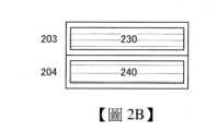
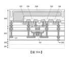
<疊層結構>圖1是說明本發明的一個實施方式的攝像裝置的剖面立體圖。攝像裝置包括層201、層202、層203、層204及層205。<Layered structure> Figure 1 is a cross-sectional perspective view of a camera device for illustrating an embodiment of the present invention. The camera device includes
注意,在本實施方式中,為了便於說明,將攝像裝置分割為上述五個層進行說明,各層中的組件的種類、數量、位置不侷限於本実施的說明。例如,有時層與層的邊界附近的絕緣層、佈線及插頭等組件包括在與本實施方式中說明的不同的層中。另外,也可以在各層中包括與本實施方式中說明的組件不同的組件。Note that in this embodiment, for the sake of convenience, the camera device is divided into the above five layers for description, and the types, quantities, and positions of components in each layer are not limited to the description of this embodiment. For example, components such as insulating layers, wiring, and plugs near the boundaries between layers may be included in a layer different from that described in this embodiment. In addition, components different from those described in this embodiment may also be included in each layer.
層201包括區域210。例如,可以在區域210設置像素電路的讀出電路、記憶體電路的驅動電路等。The
層202包括區域220。例如,可以在區域220設置記憶體電路等。
層203包括區域230。例如,可以在區域230設置像素電路(光電轉換器件240除外)及像素電路的驅動電路等。The
層204包括光電轉換器件240。作為光電轉換器件240,例如可以使用光電二極體等。光電轉換器件240是像素電路的組件。The
層205包括光學轉換層250。作為光學轉換層250,例如可以使用濾色片等。另外,層205可以包括微透鏡陣列255。The
如上所述,本發明的一個實施方式的攝像裝置包括光電轉換器件240、設置在區域230的像素電路及像素電路的驅動電路、設置在區域220的記憶體電路、設置在區域210的像素電路的讀出電路及記憶體電路的驅動電路等。As described above, an imaging device according to an embodiment of the present invention includes a
在此,光電轉換器件240較佳為對可見光具有靈敏度。例如,作為光電轉換器件240可以使用將矽用於光電轉換層的Si光電二極體。Here, the
作為像素電路及像素電路的驅動電路等的組件,較佳為使用在通道形成區域包含金屬氧化物的電晶體(以下,稱為OS電晶體)。OS電晶體的關態電流(off-state current)極小,可以抑制從像素電路流出過量資料。因此,可以使用簡單的電路結構進行在多個像素電路中一齊取得資料而依次讀出的全局快門方式工作。另外,像素的驅動電路可以藉由與像素電路相同的製程形成。As components such as pixel circuits and pixel circuit driver circuits, it is preferred to use a transistor containing a metal oxide in the channel forming region (hereinafter referred to as an OS transistor). The off-state current of the OS transistor is extremely small, which can suppress the excessive data from flowing out of the pixel circuit. Therefore, a global shutter method can be used to obtain data in multiple pixel circuits at the same time and read out in sequence using a simple circuit structure. In addition, the pixel driver circuit can be formed by the same process as the pixel circuit.
較佳為作為記憶體電路也使用OS電晶體。藉由作為記憶體電路的單元電晶體使用OS電晶體,可以抑制流出過量資料而可以抑制更新頻率。因此,可以抑制功耗。It is preferable to use an OS transistor as a memory circuit as well. By using an OS transistor as a unit transistor of a memory circuit, it is possible to suppress the excessive outflow of data and suppress the refresh frequency. Therefore, power consumption can be suppressed.
像素電路的讀出電路及記憶體電路的驅動電路等被要求高速工作,所以較佳為使用移動率高的電晶體。例如,較佳為使用在通道形成區域包含矽的電晶體(以下,稱為Si電晶體)。作為Si電晶體,可以舉出包含非晶矽的電晶體、包含結晶矽(微晶矽、低溫多晶矽、單晶矽)的電晶體等。另外,像素電路的驅動電路也可以由Si電晶體形成。The readout circuit of the pixel circuit and the drive circuit of the memory circuit are required to operate at high speed, so it is preferable to use a transistor with a high mobility. For example, it is preferable to use a transistor containing silicon in the channel forming region (hereinafter referred to as a Si transistor). As Si transistors, there can be cited transistors containing amorphous silicon, transistors containing crystalline silicon (microcrystalline silicon, low-temperature polycrystalline silicon, single crystal silicon), etc. In addition, the drive circuit of the pixel circuit can also be formed by a Si transistor.
在層疊多個Si器件時,需要進行多次的拋光製程、貼合製程。因此,製造成本高且有如下課題:製程數多、需要專用的裝置、良率低等。在本發明的一個實施方式中,藉由在Si器件上形成使用OS電晶體的電路,可以減少拋光製程及貼合製程。When stacking multiple Si devices, multiple polishing processes and bonding processes are required. Therefore, the manufacturing cost is high and there are the following problems: many processes, the need for dedicated equipment, low yield, etc. In one embodiment of the present invention, by forming a circuit using OS transistors on Si devices, the polishing process and bonding process can be reduced.
OS電晶體可以隔著絕緣層在Si器件(Si電晶體、Si光電二極體)上形成而不需要貼合、凸塊接合等複雜的製程。OS transistors can be formed on Si devices (Si transistors, Si photodiodes) through an insulating layer without the need for complex processes such as bonding and bump bonding.
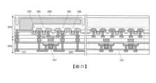
因此,在本發明的一個實施方式中,層201為包括矽基板的層,在區域210形成包括Si電晶體的電路。並且,如圖2A所示,在層201上形成層202。在層202的區域220形成包括OS電晶體的電路。Therefore, in one embodiment of the present invention,
另外,層204為包含矽基板的層,在層204作為光電轉換器件240形成Si光電二極體。並且,如圖2B所示,在層204上形成層203。在層203的區域230形成包括OS電晶體的電路。In addition, the
然後,如圖2C所示,藉由在面A貼合層202與層203,可以製造層201至層204彼此重疊的疊層結構。圖1示出在圖2C所示的疊層體的層204上還設置層205的結構。Then, as shown in Fig. 2C, by laminating
在層疊Si器件的情況下,在層疊四層時拋光製程和貼合製程至少需要進行三次左右,但是在本發明的一個實施方式中,拋光製程可以進行一次或兩次且貼合製程可以進行一次。In the case of stacked Si devices, the polishing process and the bonding process need to be performed at least three times when four layers are stacked, but in one embodiment of the present invention, the polishing process can be performed once or twice and the bonding process can be performed once.
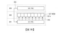
<電路>圖3A是說明層201至203所包括的組件的電連接的簡單的方塊圖。注意,層204所包括的光電轉換器件240在電路上包括在像素電路331(PIX),所以在此未圖示。<Circuit> Figure 3A is a simple block diagram illustrating the electrical connections of the components included in
像素電路331以矩陣狀排列且透過佈線351與驅動電路332(Driver)電連接。驅動電路332可以進行像素電路331的取得資料工作及選擇工作等的控制。作為驅動電路332,例如可以使用移位暫存器等。The
另外,像素電路331透過佈線352與讀出電路311(RC)電連接。讀出電路311具有去除雜訊的相關雙取樣電路(CDS電路)及將類比資料轉換為數位資料的A/D轉換器。In addition, the
讀出電路311透過佈線353與記憶體電路321(MEM)電連接。記憶體電路321可以保持從讀出電路311輸出的數位資料。或者,也可以從讀出電路311直接向外部輸出數位資料。The
記憶體電路321透過佈線354與行驅動器312(RD)電連接。另外,記憶體電路321透過佈線355與列驅動器313(CD)電連接。行驅動器312是記憶體電路321的驅動電路,可以控制資料的寫入及讀出。列驅動器313是記憶體電路321的驅動電路,可以控制資料的讀出。The
使用圖3B的方塊圖說明像素電路331、讀出電路311及記憶體電路321的詳細的連接關係。讀出電路311的數量可以與像素電路331的數量相同,每一個讀出電路311透過佈線352與每一個像素電路331電連接。另外,讀出電路311與多個佈線353連接,佈線353的每一個與一個記憶單元321a電連接。另外,也可以在讀出電路311與記憶體電路321間設置資料保持電路。The detailed connection relationship between the
讀出電路311所包括的A/D轉換器並列輸出相當於預定位元數的量的2值資料。因此,A/D轉換器連接到相當於該位元數的量的記憶單元321a。例如,在A/D轉換器的輸出是8位元時,連接到8個記憶單元321a。The A/D converter included in the
藉由採用上述結構,在本發明的一個實施方式的攝像裝置中可以並行進行在所有像素電路331中取得的類比資料的A/D轉換,而可以將所轉換了的數位資料直接寫入到記憶體電路321。換言之,可以以高速進行拍攝至向記憶體電路的儲存的工作。另外,也可以並行進行撮像工作、A/D轉換工作、讀出工作。By adopting the above structure, in the imaging device of one embodiment of the present invention, the A/D conversion of analog data obtained in all
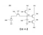
<像素電路>圖4A是說明像素電路331的一個例子的電路圖。像素電路331可以包括光電轉換器件240、電晶體103、電晶體104、電晶體105、電晶體106及電容器108。另外,也可以不設置電容器108。<Pixel circuit> Figure 4A is a circuit diagram illustrating an example of a
光電轉換器件240的一方電極(陰極)與電晶體103的源極和汲極中的一方電連接。電晶體103的源極和汲極中的另一方與電晶體104的源極和汲極中的一方電連接。電晶體104的源極和汲極中的一方與電容器108的一方電極電連接。電容器108的一方電極與電晶體105的閘極電連接。電晶體105的源極和汲極中的一方與電晶體106的源極和汲極中的一方電連接。One electrode (cathode) of the
在此,將使電晶體103的源極和汲極中的另一方、電容器108的一方電極與電晶體105的閘極連接的佈線設為節點FD。節點FD可以被用作電荷檢測部。Here, a wiring connecting the other of the source and the drain of the
光電轉換器件240的另一方電極(陽極)與佈線121電連接。電晶體103的閘極與佈線127電連接。電晶體104的源極和汲極中的另一方與佈線122電連接。電晶體105的源極和汲極中的另一方與佈線123電連接。電晶體104的閘極與佈線126電連接。電晶體106的閘極與佈線128電連接。電容器108的另一方電極例如與GND佈線等參考電位線電連接。電晶體106的源極和汲極中的另一方與佈線352電連接。The other electrode (anode) of the
佈線127、126、128可以具有作為控制各電晶體的導通的信號線的功能。佈線352可以具有作為輸出線的功能。The
佈線121、122、123可以具有作為電源線的功能。圖4A所示的結構是光電轉換器件240的陰極一側與電晶體103電連接且使節點FD重設到高電位而進行工作的結構,所以佈線122處於高電位(高於佈線121的電位)。The
圖4A示出光電轉換器件240的陰極與節點FD電連接的結構,但是如圖4B所示,也可以採用光電轉換器件240的陽極一側與電晶體103的源極和汲極中的一方電連接的結構。FIG4A shows a structure in which the cathode of the
該結構是使節點FD重設到低電位而進行工作的結構,所以佈線122處於低電位(低於佈線121的電位)。This structure operates by resetting the node FD to a low potential, so the
電晶體103具有控制節點FD的電位的功能。電晶體104具有使節點FD的電位重設的功能。電晶體105被用作源極隨耦電路的組件,可以將節點FD的電位作為影像資料輸出到佈線352。電晶體106具有選擇輸出影像資料的像素的功能。
像素電路331所包括的電晶體103至106較佳為使用OS電晶體。OS電晶體具有關態電流極低的特性。尤其是,藉由作為電晶體103、104使用關態電流低的電晶體,可以儘量延長能夠在節點FD中保持電荷的期間。因此,可以採用在所有像素中同時進行電荷的積累工作的全局快門方式而不使電路結構、工作方法複雜。The
另外,像素電路331也可以具有圖4C所示的結構。圖4C所示的像素電路331具有對圖4A的結構追加電晶體107的結構。In addition, the
電晶體107的源極和汲極中的一方與電晶體103的源極和汲極中的另一方及電晶體104的源極和汲極中的一方電連接。電晶體107的源極和汲極中的另一方與電晶體105的閘極及電容器108的一方電極電連接。電晶體107的閘極與佈線129電連接。佈線129可以具有作為控制電晶體的導通的信號線的功能。One of the source and the drain of the
將該結構中的使電晶體107的另一方電極、電晶體105的閘極及電容器108的一方電極連接的佈線設為節點FD。In this structure, a wiring connecting the other electrode of the
電晶體107具有抑制節點FD的電荷的流出的功能。因此,作為電晶體107較佳為使用關態電流較低的OS電晶體。也可以說由電晶體107及電容器108構成記憶體電路MEM。The
藉由採用該結構,即使作為電晶體103及電晶體104使用關態電流較高的Si電晶體也可以抑制電荷從節點FD流出。By adopting this structure, even if Si transistors with high off-state current are used as
因此,即使其他電晶體都是Si電晶體,只要電晶體107為OS電晶體,節點FD就呈現優良的保持特性。例如,在OS電晶體的洩漏電流為1zA、Si電晶體的洩漏電流為30fA、電容器108的電容為20fF時,估計為:在圖框頻率為60Hz的情況下,在沒有電晶體107時節點FD的電位下降25mV,在設有電晶體107時節點FD的電位下降0.83nV。Therefore, even if the other transistors are all Si transistors, as long as
如此,藉由作為電晶體107使用OS電晶體,該結構的像素電路331可以提高像素中的資料的保持功能且適於全局快門方式的工作。另外,可以將Si電晶體用於電晶體107以外的電晶體,所以可以進行高速工作。Thus, by using an OS transistor as the
另外,如圖5A、圖5B所示,也可以採用在電晶體中設置背閘極的結構。圖5A示出背閘極與前閘極電連接的結構,具有提高通態電流的效果。圖5B示出背閘極與能夠供應恆電位的佈線電連接的結構,該結構可以控制電晶體的臨界電壓。In addition, as shown in FIG5A and FIG5B, a structure in which a back gate is provided in the transistor can also be adopted. FIG5A shows a structure in which the back gate is electrically connected to the front gate, which has the effect of increasing the on-state current. FIG5B shows a structure in which the back gate is electrically connected to a wiring capable of supplying a constant potential, which can control the critical voltage of the transistor.
另外,也可以使各電晶體可以進行適當的工作,諸如組合圖5A、圖5B所示的電晶體的結構等。另外,像素電路331也可以包括不設置有背閘極的電晶體。注意,圖5A、圖5B示出在圖4A所示的像素電路331中設置背閘極的例子,但是也可以適用於圖4B、圖4C的像素電路331。In addition, each transistor can be made to work properly, such as by combining the structures of the transistors shown in FIG. 5A and FIG. 5B. In addition, the
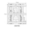
圖6A、圖6B是示出圖5B所示的像素電路331的佈局的一個例子的俯視圖。為了明確像素電路331的各組件,圖6A示出電容器108的到上部電極的層。另外,圖6B還追加示出使各組件間或各組件與驅動電路連接的佈線。圖6A、圖6B示出使電晶體尺寸設為W/L=60nm/60nm的例子,可以在1.2μm×1.3μm的區域安裝組件。FIG. 6A and FIG. 6B are top views showing an example of the layout of the
<讀出電路>圖7是說明與像素電路331連接的讀出電路311的一個例子的圖,示出CDS電路400的電路圖及與CDS電路400電連接的A/D轉換器410的方塊圖。注意,圖7所示的CDS電路及A/D轉換器是一個例子,也可以採用其他結構。<Readout circuit> Figure 7 is a diagram illustrating an example of a
CDS電路400可以採用包括電壓轉換用電晶體401、電容耦合用電容器402、供應電位V0的電晶體403、保持供應到A/D轉換器410的電位的電晶體404、以及電位保持用電容器405的結構。CDS電路400的輸入電連接到像素電路331且輸出電連接到A/D轉換器410的比較器電路(COMP)。The
在佈線352的電位為Vres+Vdata(重設電位+影像資料的電位)時,節點N(電晶體403、404與電容器402的連接點)的電位設為V0。此外,在使節點N處於浮動狀態而將佈線352的電位設為Vres(重設電位)時,由於電容器402的電容耦合,對節點N追加佈線352的電位變化的量。因此,節點N的電位為V0+((Vres+Vdata)-Vres),在V0=0時只殘留Vdata的項。Vres包括伴隨電晶體的工作的雜訊成分,所以可以去除該雜訊成分。When the potential of
A/D轉換器410可以包括比較器電路(COMP)及計數電路(COUNTER)。在A/D轉換器410中,比較從CDS電路400輸入到比較器電路(COMP)的信號電位和被掃描的參考電位(RAMP)。此外,計數電路(COUNTER)根據比較器電路(COMP)的輸出進行工作而對多個佈線353輸出數位信號。The A/
<記憶體電路>圖8A是示出記憶體電路321所包括的記憶單元321a、行驅動器312與列驅動器313的連接關係的圖。作為構成記憶單元321a的電晶體可以使用OS電晶體。<Memory Circuit> Figure 8A is a diagram showing the connection relationship between the
記憶體電路321包括在一個列上m(m為1以上的整數)個且在一個行上n(n為1以上的整數)個,共m×n個的記憶單元321a,記憶單元321a以矩陣狀配置。圖8A也示出記憶單元321a的位址。例如,[1,1]表示位於第1行第1列的位址的記憶單元321a,[i,j](i為1以上且m以下的整數、j為1以上且n以下的整數)表示位於第i行第j列的位址的記憶單元321a。使記憶體電路321與行驅動器312連接的佈線的數量根據記憶單元321a的結構、一個列上的記憶單元321a的數量等而決定。另外,使記憶體電路321與列驅動器313連接的佈線的數量根據記憶單元321a的結構、一行上的記憶單元321a的數量等而決定。The
圖8B至圖8E是說明能夠適用於記憶單元321a的記憶單元321aA至記憶單元321aD的圖。注意,在以下說明中,位元線類可以連接到列驅動器313。另外,字線類可以連接到行驅動器312。注意,位元線類也連接到讀出電路311,但是在此未圖示。8B to 8E are diagrams illustrating memory cells 321aA to 321aD applicable to the
作為行驅動器312及列驅動器313,例如可以使用解碼器或移位暫存器。另外,也可以設置多個行驅動器312及多個列驅動器313。For example, a decoder or a shift register may be used as the
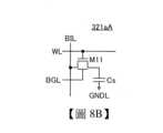
[DOSRAM]圖8B示出DRAM型的記憶單元321aA的電路結構例子。在本說明書等中,將使用OS電晶體的DRAM稱為DOSRAM(Dynamic Oxide Semiconductor Random Access Memory:動態氧化物半導體隨機存取記憶體)。記憶單元321aA包括電晶體M11及電容器Cs。[DOSRAM]Figure 8B shows an example of the circuit structure of a DRAM-type memory cell 321aA. In this specification, etc., a DRAM using an OS transistor is referred to as a DOSRAM (Dynamic Oxide Semiconductor Random Access Memory). The memory cell 321aA includes a transistor M11 and a capacitor Cs.
電晶體M11的第一端子與電容器Cs的第一端子連接,電晶體M11的第二端子與佈線BIL連接,電晶體M11的閘極與佈線WL連接,電晶體M11的背閘極與佈線BGL連接。電容器Cs的第二端子與佈線GNDL連接。佈線GNDL是供應低位準電位(也稱為參考電位)的佈線。The first terminal of the transistor M11 is connected to the first terminal of the capacitor Cs, the second terminal of the transistor M11 is connected to the wiring BIL, the gate of the transistor M11 is connected to the wiring WL, and the back gate of the transistor M11 is connected to the wiring BGL. The second terminal of the capacitor Cs is connected to the wiring GNDL. The wiring GNDL is a wiring for supplying a low potential (also called a reference potential).
佈線BIL被用作位元線。佈線WL被用作字線。佈線BGL用作對電晶體M11的背閘極施加電位的佈線。藉由對佈線BGL施加任意電位,可以增減電晶體M11的臨界電壓。The wiring BIL is used as a bit line. The wiring WL is used as a word line. The wiring BGL is used as a wiring for applying a potential to the back gate of the transistor M11. By applying an arbitrary potential to the wiring BGL, the critical voltage of the transistor M11 can be increased or decreased.
資料的寫入及讀出藉由對佈線WL施加高位準電位使電晶體M11變為導通狀態而使佈線BIL與電容器Cs的第一端子電連接而進行。Data writing and reading are performed by applying a high potential to the wiring WL to turn on the transistor M11 and thereby electrically connecting the wiring BIL to the first terminal of the capacitor Cs.
作為電晶體M11較佳為使用OS電晶體。另外,OS電晶體的半導體層較佳為使用含有銦、元素M(元素M為鋁、鎵、釔和錫中的一個或多個)、鋅中的任意一個的氧化物半導體。尤其是,較佳為使用包含銦、鎵及鋅的氧化物半導體。It is preferable to use an OS transistor as the transistor M11. In addition, it is preferable to use an oxide semiconductor containing any one of indium, element M (element M is one or more of aluminum, gallium, yttrium and tin), and zinc as the semiconductor layer of the OS transistor. In particular, it is preferable to use an oxide semiconductor containing indium, gallium and zinc.
使用含有銦、鎵、鋅的氧化物半導體的OS電晶體具有關態電流極小的特性。藉由作為電晶體M11使用OS電晶體,可以使電晶體M11的洩漏電流非常低。也就是說,可以利用電晶體M11長時間地保持寫入資料,由此可以降低記憶單元的更新頻率。或者,可以無需進行記憶單元的更新工作。OS transistors using oxide semiconductors containing indium, gallium, and zinc have the characteristic of extremely low off-state current. By using OS transistors as transistor M11, the leakage current of transistor M11 can be made very low. In other words, transistor M11 can be used to maintain written data for a long time, thereby reducing the update frequency of the memory cell. Alternatively, there is no need to update the memory cell.
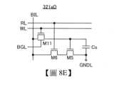
[NOSRAM]圖8C示出包括2個電晶體和1個電容器的增益單元型(也稱為“2Tr1C型”)的記憶單元321aB的電路結構例子。記憶單元321aB包括電晶體M11、電晶體M3及電容器Cs。[NOSRAM]Figure 8C shows an example of a circuit structure of a memory cell 321aB of a gain unit type (also referred to as a "2Tr1C type") including two transistors and one capacitor. The memory cell 321aB includes a transistor M11, a transistor M3, and a capacitor Cs.
電晶體M11的第一端子與電容器Cs的第一端子連接,電晶體M11的第二端子與佈線WBL連接,電晶體M11的閘極與佈線WL連接,電晶體M11的背閘極與佈線BGL連接。電容器Cs的第二端子與佈線RL連接。電晶體M3的第一端子與佈線RBL連接,電晶體M3的第二端子與佈線SL連接,電晶體M3的閘極與電容器Cs的第一端子連接。The first terminal of transistor M11 is connected to the first terminal of capacitor Cs, the second terminal of transistor M11 is connected to wiring WBL, the gate of transistor M11 is connected to wiring WL, and the back gate of transistor M11 is connected to wiring BGL. The second terminal of capacitor Cs is connected to wiring RL. The first terminal of transistor M3 is connected to wiring RBL, the second terminal of transistor M3 is connected to wiring SL, and the gate of transistor M3 is connected to the first terminal of capacitor Cs.
佈線WBL被用作寫入位元線。佈線RBL被用作讀出位元線。佈線WL被用作字線。佈線RL用作對電容器Cs的第二端子施加預定電位的佈線。資料寫入時、正在進行資料保持時,較佳為對佈線RL施加參考電位。Wiring WBL is used as a write bit line. Wiring RBL is used as a read bit line. Wiring WL is used as a word line. Wiring RL is used as a wiring for applying a predetermined potential to the second terminal of capacitor Cs. When data is written or data is retained, it is preferred to apply a reference potential to wiring RL.
佈線BGL用作對電晶體M11的背閘極施加電位的佈線。藉由對佈線BGL施加任意電位,可以增減電晶體M11的臨界電壓。The wiring BGL is used as a wiring for applying a potential to the back gate of the transistor M11. By applying an arbitrary potential to the wiring BGL, the critical voltage of the transistor M11 can be increased or decreased.
資料的寫入藉由對佈線WL施加高位準電位使電晶體M11變為導通狀態以使佈線WBL與電容器Cs的第一端子電連接來進行。明確地說,在電晶體M11為導通狀態時,對佈線WBL施加對應於要記錄的資訊的電位來對電容器Cs的第一端子及電晶體M3的閘極寫入該電位。然後,對佈線WL施加低位準電位使電晶體M11變為非導通狀態,由此儲存電容器Cs的第一端子的電位及電晶體M3的閘極的電位。Data is written by applying a high potential to the wiring WL to turn the transistor M11 into a conductive state so that the wiring WBL is electrically connected to the first terminal of the capacitor Cs. Specifically, when the transistor M11 is in a conductive state, a potential corresponding to the information to be recorded is applied to the wiring WBL to write the potential to the first terminal of the capacitor Cs and the gate of the transistor M3. Then, a low potential is applied to the wiring WL to turn the transistor M11 into a non-conductive state, thereby storing the potential of the first terminal of the capacitor Cs and the potential of the gate of the transistor M3.
資料的讀出藉由對佈線RL和佈線SL施加預定的電位來進行。由於電晶體M3的源極-汲極間流過的電流及電晶體M3的第一端子的電位由電晶體M3的閘極的電位及電晶體M3的第二端子的電位決定,所以藉由讀出與電晶體M3的第一端子連接的佈線RBL的電位,可以讀出電容器Cs的第一端子(或電晶體M3的閘極)所保持的電位。也就是說,可以從電容器Cs的第一端子(或電晶體M3的閘極)所保持的電位讀出該記憶單元中寫入的資訊。或者,可以知道該記憶單元是否被寫入資訊。Data is read by applying a predetermined potential to the wiring RL and the wiring SL. Since the current flowing between the source and drain of the transistor M3 and the potential of the first terminal of the transistor M3 are determined by the potential of the gate of the transistor M3 and the potential of the second terminal of the transistor M3, the potential held by the first terminal of the capacitor Cs (or the gate of the transistor M3) can be read by reading the potential of the wiring RBL connected to the first terminal of the transistor M3. In other words, the information written in the memory cell can be read from the potential held by the first terminal of the capacitor Cs (or the gate of the transistor M3). Alternatively, it can be known whether the memory cell has information written.
另外,如圖8D所示,也可以採用將佈線WBL與佈線RBL合為一個佈線BIL的結構。在圖8D所示的記憶單元321aC中,記憶單元321aB的佈線WBL與佈線RBL合為一個佈線BIL,電晶體M11的第二端子及電晶體M3的第一端子與佈線BIL連接。也就是說,記憶單元321aC將寫入位元線和讀出位元線合為一個佈線BIL工作。In addition, as shown in FIG8D , a structure in which the wiring WBL and the wiring RBL are combined into one wiring BIL may also be adopted. In the memory cell 321aC shown in FIG8D , the wiring WBL and the wiring RBL of the memory cell 321aB are combined into one wiring BIL, and the second terminal of the transistor M11 and the first terminal of the transistor M3 are connected to the wiring BIL. In other words, the memory cell 321aC combines the write bit line and the read bit line into one wiring BIL.
另外,記憶單元321aB及記憶單元321aC的電晶體M11也較佳為使用OS電晶體。將使用記憶單元321aB及記憶單元321aC那樣的作為電晶體M11使用OS電晶體的2Tr1C型的記憶單元的記憶體裝置稱為NOSRAM(Non-volatile Oxide Semiconductor Random Access Memory:氧化物半導體非揮發性隨機存取記憶體)。In addition, the transistor M11 of the memory cell 321aB and the memory cell 321aC is preferably an OS transistor. A memory device using a 2Tr1C type memory cell using an OS transistor as the transistor M11 such as the memory cell 321aB and the memory cell 321aC is called a NOSRAM (Non-volatile Oxide Semiconductor Random Access Memory).
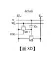
另外,圖8D示出3個電晶體1個電容器的增益單元型(也稱為“3Tr1C型”)的記憶單元321aD的電路結構例子。記憶單元321aD包括電晶體M11、電晶體M5、電晶體M6及電容器Cs。8D shows a circuit configuration example of a memory cell 321aD of a gain unit type of three transistors and one capacitor (also referred to as a "3Tr1C type"). The memory cell 321aD includes a transistor M11, a transistor M5, a transistor M6, and a capacitor Cs.
電晶體M11的第一端子與電容器Cs的第一端子連接,電晶體M11的第二端子與佈線BIL連接,電晶體M11的閘極與佈線WL連接,電晶體M11的背閘極與佈線BGL電連接。電容器Cs的第二端子與電晶體M5的第一端子、佈線GNDL電連接。電晶體M5的第二端子與電晶體M6的第一端子連接,電晶體M5的閘極與電容器Cs的第一端子連接。電晶體M6的第二端子與佈線BIL連接,電晶體M6的閘極與佈線RL連接。The first terminal of transistor M11 is connected to the first terminal of capacitor Cs, the second terminal of transistor M11 is connected to wiring BIL, the gate of transistor M11 is connected to wiring WL, and the back gate of transistor M11 is electrically connected to wiring BGL. The second terminal of capacitor Cs is electrically connected to the first terminal of transistor M5 and wiring GNDL. The second terminal of transistor M5 is connected to the first terminal of transistor M6, and the gate of transistor M5 is connected to the first terminal of capacitor Cs. The second terminal of transistor M6 is connected to wiring BIL, and the gate of transistor M6 is connected to wiring RL.
佈線BIL用作位元線,佈線WL用作寫入字線,佈線RL用作讀出字線。The wiring BIL is used as a bit line, the wiring WL is used as a write word line, and the wiring RL is used as a read word line.
佈線BGL用作對電晶體M11的背閘極施加電位的佈線。藉由對佈線BGL施加任意電位,可以增減電晶體M11的臨界電壓。The wiring BGL is used as a wiring for applying a potential to the back gate of the transistor M11. By applying an arbitrary potential to the wiring BGL, the critical voltage of the transistor M11 can be increased or decreased.
資料的寫入藉由對佈線WL施加高位準電位使電晶體M11變為導通狀態以使佈線BIL與電容器Cs的第一端子連接來進行。明確地說,在電晶體M11為導通狀態時,對佈線BIL施加對應於要記錄的資訊的電位來對電容器Cs的第一端子及電晶體M5的閘極寫入該電位。然後,對佈線WL施加低位準電位使電晶體M11變為非導通狀態,由此儲存電容器Cs的第一端子的電位及電晶體M5的閘極的電位。Data is written by applying a high potential to the wiring WL to turn the transistor M11 into a conductive state so that the wiring BIL is connected to the first terminal of the capacitor Cs. Specifically, when the transistor M11 is in a conductive state, a potential corresponding to the information to be recorded is applied to the wiring BIL to write the potential to the first terminal of the capacitor Cs and the gate of the transistor M5. Then, a low potential is applied to the wiring WL to turn the transistor M11 into a non-conductive state, thereby storing the potential of the first terminal of the capacitor Cs and the potential of the gate of the transistor M5.
資料的讀出藉由將佈線BIL預充電至預定的電位之後使佈線BIL變為電浮動狀態並對佈線RL施加高位準電位來進行。藉由使佈線RL變為高位準電位,電晶體M6變為導通狀態,佈線BIL與電晶體M5的第二端子變為電連接狀態。此時,電晶體M5的第二端子被施加佈線BIL的電位,但是電晶體M5的第二端子的電位及佈線BIL的電位會對應電容器Cs的第一端子(或電晶體M5的閘極)所保持的電位改變。這裡,可以藉由讀出佈線BIL的電位來讀出電容器Cs的第一端子(或電晶體M5的閘極)所保持的電位。也就是說,可以從電容器Cs的第一端子(或電晶體M5的閘極)所保持的電位讀出該記憶單元中寫入的資訊。或者,可以知道該記憶單元是否被寫入資訊。Data is read by precharging wiring BIL to a predetermined potential, then making wiring BIL electrically floating and applying a high level potential to wiring RL. By making wiring RL a high level potential, transistor M6 becomes conductive, and wiring BIL and the second terminal of transistor M5 become electrically connected. At this time, the potential of wiring BIL is applied to the second terminal of transistor M5, but the potential of the second terminal of transistor M5 and the potential of wiring BIL will change in accordance with the potential maintained by the first terminal of capacitor Cs (or the gate of transistor M5). Here, the potential maintained by the first terminal of capacitor Cs (or the gate of transistor M5) can be read by reading the potential of wiring BIL. That is, the information written in the memory cell can be read from the potential held by the first terminal of the capacitor Cs (or the gate of the transistor M5). Alternatively, it can be known whether the memory cell has information written therein.
另外,記憶單元321aD的電晶體M11也較佳為使用OS電晶體。作為電晶體M11使用了OS電晶體的3Tr1C型的記憶單元321aD是前面所述的NOSRAM的一個實施方式。記憶單元可以適當地改變其電路結構。In addition, the transistor M11 of the memory cell 321aD is preferably an OS transistor. The 3Tr1C memory cell 321aD using the OS transistor as the transistor M11 is an embodiment of the aforementioned NOSRAM. The circuit structure of the memory cell can be appropriately changed.
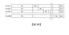
<攝像裝置的工作方式>圖9A示意性地示出滾動式快門方式的工作方法,圖9B示意性地示出全局快門方式。En表示第n列(n為自然數)的曝光(積累工作)、Rn表示第n列的讀出工作。圖9A、圖9B示出第1行(Line[1])至第M行(Line[M],M為自然數)的工作。<Working method of the camera> Figure 9A schematically shows the working method of the rolling shutter method, and Figure 9B schematically shows the working method of the global shutter method. En represents the exposure (accumulation operation) of the nth column (n is a natural number), and Rn represents the reading operation of the nth column. Figures 9A and 9B show the operation of the 1st row (Line[1]) to the Mth row (Line[M], M is a natural number).
滾動式快門方式是依次進行曝光及資料讀出的工作方法,其中一個行的讀出期間與其他行的曝光期間重疊。曝光後立刻進行讀出工作,所以即使使用資料的保持期間較短的電路結構也可以進行撮像。但是,由於由沒有撮像的同時性的資料構成1個圖框的影像,所以在拍攝動體時在影像中產生歪曲。The rolling shutter method is a method of sequentially performing exposure and data readout, where the readout period of one row overlaps the exposure period of other rows. Since the readout operation is performed immediately after exposure, it is possible to capture images even with a circuit structure that has a short data retention period. However, since an image of one frame is formed by data that is not captured synchronously, distortion occurs in the image when shooting a moving object.
另一方面,全局快門方式是在所有像素中同時進行曝光而在各像素保持資料,按每個行讀出資料的工作方法。因此,在動體的撮像中也可以得到沒有歪曲的影像。On the other hand, the global shutter method is a method of operating in which all pixels are exposed at the same time, data is stored in each pixel, and data is read out for each row. Therefore, even when shooting moving objects, images without distortion can be obtained.
在作為像素電路使用Si電晶體等關態電流較高的電晶體時,電荷容易從電荷檢測部流出,所以多採用滾動式快門方式。為了使用Si電晶體實現全局快門方式,需要以高速進行複雜的工作,諸如另行將資料儲存於記憶體電路等。另一方面,在作為像素電路使用OS電晶體時,從電荷檢測部幾乎沒有流出資料電位,所以容易實現全局快門方式。另外,本發明的一個實施方式的攝像裝置可以藉由滾動式快門方式工作。When a transistor with a high off-state current such as an Si transistor is used as a pixel circuit, the charge easily flows out from the charge detection part, so a rolling shutter method is often used. In order to use Si transistors to implement a global shutter method, complex operations need to be performed at high speed, such as storing data separately in a memory circuit. On the other hand, when an OS transistor is used as a pixel circuit, almost no data potential flows out from the charge detection part, so it is easy to implement a global shutter method. In addition, a camera device of an embodiment of the present invention can work by a rolling shutter method.
另外,像素電路331也可以採用任意地組合OS電晶體及Si電晶體的結構。或者,也可以作為所有電晶體使用Si電晶體。In addition, the
<像素電路的工作><Pixel circuit operation>
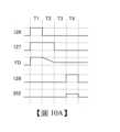
接著,用圖10A的時序圖說明圖4A所示的像素電路331的工作的一個例子。在本說明書中的時序圖的說明中,以“H”表示高電位,以“L”表示低電位。對佈線121一直供應“L”且對佈線122、123一直供應“H”。Next, an example of the operation of the
在期間T1,當佈線126的電位設為“H”、佈線127的電位設為“H”、佈線128的電位設為“L”時,電晶體103、104導通而對節點FD供應佈線122的電位“H”(重設工作)。In period T1, when the potential of
在期間T2,當佈線126的電位設為“L”、佈線127的電位設為“H”、佈線128的電位設為“L”時,電晶體104不導通而停止重設電位的供應。另外,節點FD的電位對應光電轉換器件240的工作下降(積累工作)。In period T2, when the potential of
在期間T3,當佈線126的電位設為“L”、佈線127的電位設為“L”、佈線128的電位設為“L”時,電晶體103不導通,節點FD的電位確定而被保持(保持工作)。此時,藉由作為連接到節點FD的電晶體103及電晶體104使用關態電流較低的OS電晶體,可以抑制從節點FD流出過量電荷,所以可以延長資料的保持時間。In period T3, when the potential of
在期間T4,當佈線126的電位設為“L”、佈線127的電位設為“L”、佈線128的電位設為“H”時,電晶體106導通,節點FD的電位根據電晶體105的源極隨耦工作被讀出到佈線352(讀出工作)。In period T4, when the potential of
以上是圖4A所示的像素電路331的工作的一個例子。The above is an example of the operation of the
圖4B所示的像素電路331可以根據圖10B的時序圖進行工作。注意,對佈線121、123一直供應“H”且對佈線122一直供應“L”。基本工作與上述圖10A的時序圖的說明相同。The
圖4C所示的像素電路331可以根據圖10C的時序圖進行工作。在圖4C的像素電路331中,藉由按每個行控制佈線129,可以容易進行CDS電路400中的讀出工作。因此,也說明CDS電路400的工作。注意,電晶體401(參照圖7)的閘極被供應適當的類比電位。The
在期間T1,當佈線126的電位設為“L”、佈線127的電位設為“L”、佈線128的電位設為“L”、佈線129的電位設為“H”時,電晶體107導通。In the period T1, when the potential of the
接著,在期間T2,當佈線126的電位設為“H”、佈線127的電位設為“L”、佈線128的電位設為“L”、佈線129的電位設為“H”時,電晶體104導通而對節點FD供應佈線122的電位“H”(重設電位)(重設工作)。Next, during period T2, when the potential of
接著,在期間T3,當佈線126的電位設為“L”、佈線127的電位設為“L”、佈線128的電位設為“L”、佈線129的電位設為“H”時,電晶體104不導通而節點FD保持為重設電位。Next, in period T3, when the potential of
在期間T4,當佈線126的電位設為“L”、佈線127的電位設為“H”、佈線128的電位設為“L”、佈線129的電位設為“H”時,電晶體103導通而節點FD的電位對應光電轉換器件240的工作下降(轉送工作)。During period T4, when the potential of
在期間T5,當佈線126的電位設為“L”、佈線127的電位設為“L”、佈線128的電位設為“L”、佈線129的電位設為“H”時,電晶體103不導通而節點FD的電位確定。In the period T5, when the potential of the
在期間T6,當佈線126的電位設為“L”、佈線127的電位設為“L”、佈線128的電位設為“L”、佈線129的電位設為“L”時,電晶體107不導通而節點FD的電位被保持(保持工作)。此時,藉由作為連接到節點FD的電晶體107使用關態電流較低的OS電晶體,可以抑制從節點FD流出過量電荷,所以可以延長資料的保持時間。In period T6, when the potential of
在期間T7,當佈線126的電位設為“L”、佈線127的電位設為“L”、佈線128的電位設為“H”、佈線129的電位設為“L”、佈線431(參照圖7)的電位設為“H”時,電晶體106導通,節點FD的電位根據電晶體105的源極隨耦工作被讀出到佈線352(讀出工作)。During period T7, when the potential of
另外,在CDS電路400(參照圖7)中,電晶體403導通且節點N重設到佈線432的電位“Vr”。換言之,在與佈線352電連接的電容器402的一方電極的電位處於像素電路331輸出影像資料的狀態下,節點N(電容器402的另一方的電極)被初始化為電位“Vr”。In addition, in the CDS circuit 400 (see FIG. 7 ), the
在期間T8,當佈線126的電位設為“L”、佈線127的電位設為“L”、佈線128的電位設為“H”、佈線129的電位設為“H”、佈線431的電位設為“L”時,電晶體107導通。另外,節點N的電位保持為電位“Vr”。In period T8, when the potential of
在期間T9,當佈線126的電位設為“H”、佈線127的電位設為“L”、佈線128的電位設為“H”、佈線129的電位設為“H”、佈線431的電位設為“L”時,電晶體104導通而對節點FD供應佈線122的電位“H”(重設電位)。During period T9, when the potential of
藉由在時刻T10佈線126的電位設為“L”且在時刻T11佈線129的電位設為“L”,使電晶體104及電晶體107不導通而將節點FD的電位保持為重設電位。By setting the potential of the
並且,藉由伴隨節點FD的電位變化的源極隨耦工作,電容器402的一方電極的電位變化而該變化Y由電容耦合追加到節點N的電位“Vr”。因此,節點N的電位成為“Vr+Y”。在此,Y是不包括重設電位成分的影像資料,讀出雜訊成分被去除的資料。Furthermore, due to the source follower operation accompanying the potential change of the node FD, the potential of one electrode of the
<疊層結構1>接著,使用剖面圖說明攝像裝置的疊層結構。<
圖11示出包括層201至層205且在層202與層203間具有接合平面的疊層體的剖面圖的一個例子。FIG. 11 shows an example of a cross-sectional view of a stacked
<層201>層201包括設置在矽基板211上的讀出電路311、行驅動器312及列驅動器313。在此,作為上述電路的一部分示出讀出電路311的CDS電路所包括的電容器402及電晶體403、讀出電路311的A/D轉換器所包括的電晶體115以及行驅動器312所包括的電晶體116。電容器402的一方電極與電晶體403的源極和汲極中的一方電連接。<Layer 201>
在層201中設置絕緣層212、213、214、215、216、217、218。絕緣層212具有作為保護膜的功能。絕緣層212、213、214、217具有作為層間絕緣膜及平坦化膜的功能。絕緣層216具有作為電容器402的介電質層的功能。絕緣層218具有作為障壁膜的功能。Insulating
作為保護膜,例如可以使用氮化矽膜、氧化矽膜、氧化鋁膜等。作為層間絕緣膜及平坦化膜,例如可以使用氧化矽膜等的無機絕緣膜、丙烯酸樹脂、聚醯亞胺樹脂等的有機絕緣膜。作為電容器的介電質層,可以使用氮化矽膜、氧化矽膜、氧化鋁膜等。作為障壁膜,較佳為使用具有抑制氫的擴散的功能的膜。As a protective film, for example, a silicon nitride film, a silicon oxide film, an aluminum oxide film, etc. can be used. As an interlayer insulating film and a planarizing film, for example, an inorganic insulating film such as a silicon oxide film, an organic insulating film such as an acrylic resin, a polyimide resin, etc. can be used. As a dielectric layer of a capacitor, a silicon nitride film, a silicon oxide film, an aluminum oxide film, etc. can be used. As a barrier film, it is preferable to use a film having a function of suppressing the diffusion of hydrogen.
在Si器件中,為了使懸空鍵終結需要氫,但是OS電晶體附近的氫成為在氧化物半導體層中產生載子的原因之一而降低可靠性。因此,在形成Si器件的層與形成OS電晶體的層間較佳為設置氫的障壁膜。In Si devices, hydrogen is required to terminate dangling bonds, but hydrogen near the OS transistor becomes one of the causes of carrier generation in the oxide semiconductor layer, reducing reliability. Therefore, it is preferable to provide a hydrogen barrier film between the layer forming the Si device and the layer forming the OS transistor.
作為該障壁膜,例如可以使用氧化鋁、氧氮化鋁、氧化鎵、氧氮化鎵、氧化釔、氧氮化釔、氧化鉿、氧氮化鉿、釔安定氧化鋯(YSZ)等。As the barrier film, for example, aluminum oxide, aluminum oxynitride, gallium oxide, gallium oxynitride, yttrium oxide, yttrium oxynitride, einsteinium oxide, einsteinium oxynitride, yttrium-stabilized zirconia (YSZ), or the like can be used.
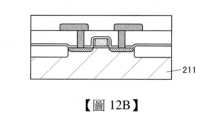
圖11所示的Si電晶體是在矽基板211具有通道形成區域的鰭型,圖12A示出通道寬度方向的剖面(圖11所示的A1-A2的剖面)。如圖12B所示,Si電晶體也可以為平面型。The Si transistor shown in FIG11 is a fin type having a channel forming region on a
另外,如圖12C所示,也可以採用包括矽薄膜的半導體層545的電晶體。例如,半導體層545可以使用在矽基板211上的絕緣層546上形成的單晶矽(SOI(Silicon on Insulator:絕緣層上覆矽))。12C , a transistor including a
作為可以作為用於器件間的電連接的佈線、電極及插頭使用的導電體,適當地選擇選自鋁、鉻、銅、銀、金、鉑、鉭、鎳、鈦、鉬、鎢、鉿、釩、鈮、錳、鎂、鋯、鈹、銦、釕、銥、鍶和鑭等中的金屬元素、以上述金屬元素為成分的合金或者組合上述金屬元素的合金等而使用即可。該導電體既可以為單層又可以為由不同材料構成的多個層。As a conductor that can be used as wiring, electrodes and plugs for electrical connection between devices, metal elements selected from aluminum, chromium, copper, silver, gold, platinum, tungsten ...
<層202>層202形成在層201上。層202包括具有OS電晶體的記憶體電路321。在此,作為記憶體電路321的一部分示出記憶單元321a所包括的電晶體111及電容器112。<Layer 202>
在層202中設置絕緣層221、222、223、224、225、226、227、228、229。另外,設置導電層131。Insulating
絕緣層221、224、225、227、228具有作為層間絕緣膜及平坦化膜的功能。絕緣層222具有作為閘極絕緣膜的功能。絕緣層223具有作為保護膜的功能,絕緣層226具有作為電容器的介電質層的功能。絕緣層229及導電層131具有作為貼合層的功能。The insulating
作為閘極絕緣膜可以使用氧化矽膜等。關於貼合層,在後面說明。As the gate insulating film, a silicon oxide film or the like can be used. The bonding layer will be described later.
導電層131與層201的電容器402的另一方電極電連接。電晶體111的源極和汲極中的一方與層201的電晶體115的源極和汲極中的一方電連接。電晶體111的閘極與層201的電晶體116的源極和汲極中的一方電連接。電晶體111的源極和汲極中的另一方與電容器112的一方電極電連接。
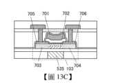
圖13A示出詳細的OS電晶體。圖13A所示的OS電晶體具有藉由在氧化物半導體層及導電層的疊層上設置絕緣層而設置到達該氧化物半導體層的開口部來形成源極電極705及汲極電極706的自對準型的結構。Fig. 13A shows a detailed OS transistor. The OS transistor shown in Fig. 13A has a self-aligned structure in which a
除了形成在氧化物半導體層的通道形成區域、源極區域703及汲極區域704以外,OS電晶體還可以包括閘極電極701、閘極絕緣膜702。在該開口部中至少設置閘極絕緣膜702及閘極電極701。在該槽中也可以還設置氧化物半導體層707。In addition to the channel formation region,
如圖13B所示,OS電晶體也可以採用使用閘極電極701作為遮罩在半導體層形成源極區域703及汲極區域704的自對準型的結構。As shown in FIG. 13B , the OS transistor may also adopt a self-aligned structure in which a
或者,如圖13C所示,可以採用具有源極電極705或汲極電極706與閘極電極701重疊的區域的非自對準型的頂閘極型電晶體。Alternatively, as shown in FIG. 13C , a non-self-aligned top gate transistor having a region where the
OS電晶體包括背閘極535,但也可以不包括背閘極。如圖13D所示的電晶體的通道寬度方向的剖面圖那樣,背閘極535也可以與相對的電晶體的前閘極電連接。作為一個例子,圖13D示出圖13A所示的B1-B2的剖面,其他結構的電晶體也是同樣的。另外,也可以採用能夠對背閘極535供應與前閘極不同的固定電位的結構。The OS transistor includes a
作為用於OS電晶體的半導體材料,可以使用能隙為2eV以上,較佳為2.5eV以上,更佳為3eV以上的金屬氧化物。典型的有含有銦的氧化物半導體等,例如,可以使用後面提到的CAAC-OS或CAC-OS等。CAAC-OS中構成晶體的原子穩定,適用於重視可靠性的電晶體等。CAC-OS呈現高移動率特性,適用於進行高速驅動的電晶體等。As semiconductor materials for OS transistors, metal oxides with energy gaps of 2 eV or more, preferably 2.5 eV or more, and more preferably 3 eV or more can be used. Typical examples include oxide semiconductors containing indium, and for example, CAAC-OS or CAC-OS mentioned later can be used. CAAC-OS has stable atoms constituting the crystal, and is suitable for transistors that value reliability. CAC-OS has high mobility characteristics, and is suitable for transistors that are driven at high speeds.
由於OS電晶體的半導體層具有大能隙,所以呈現極低的關態電流特性,僅為幾yA/μm(每通道寬度1μm的電流值)。與Si電晶體不同,OS電晶體不會發生碰撞電離、突崩潰、短通道效應等,因此能夠形成高耐壓性和高可靠性的電路。此外,Si電晶體所引起的起因於結晶性的不均勻的電特性不均勻不容易產生在OS電晶體中。Since the semiconductor layer of OS transistors has a large energy gap, they exhibit extremely low off-state current characteristics of only a few yA/μm (current value per channel width of 1μm). Unlike Si transistors, OS transistors do not experience impact ionization, sudden collapse, short channel effects, etc., so they can form circuits with high voltage resistance and high reliability. In addition, the electrical characteristics unevenness caused by the uneven crystallinity caused by Si transistors is not easy to occur in OS transistors.
作為OS電晶體中的半導體層,例如可以採用包含銦、鋅及M(鋁、鈦、鎵、鍺、釔、鋯、鑭、鈰、錫、釹和鉿等金屬中的一個或多個)的以“In-M-Zn類氧化物”表示的膜。典型的是,In-M-Zn類氧化物可以藉由濺射法形成。或者,也可以藉由ALD(Atomic layer deposition:原子層沉積)法形成。As a semiconductor layer in the OS transistor, for example, a film represented by "In-M-Zn oxide" containing indium, zinc, and M (one or more of metals such as aluminum, titanium, gallium, germanium, yttrium, zirconium, lumen, niobium, tin, neodymium, and einsteinium) can be used. Typically, the In-M-Zn oxide can be formed by sputtering. Alternatively, it can also be formed by ALD (Atomic layer deposition) method.
當利用濺射法形成In-M-Zn類氧化物膜時,較佳為用來形成In-M-Zn類氧化物膜的濺射靶材的金屬元素的原子數比滿足In≥M及Zn≥M。這種濺射靶材的金屬元素的原子數比較佳為In:M:Zn=1:1:1、In:M:Zn=1:1:1.2、In:M:Zn=3:1:2、In:M:Zn=4:2:3、In:M:Zn=4:2:4.1、In:M:Zn=5:1:6、In:M:Zn=5:1:7、In:M:Zn=5:1:8等。注意,所形成的半導體層的原子數比分別有可能在上述濺射靶材中的金屬元素的原子數比的±40%的範圍內變動。When an In-M-Zn oxide film is formed by a sputtering method, it is preferred that the atomic ratio of the metal element of the sputtering target used to form the In-M-Zn oxide film satisfies In ≥ M and Zn ≥ M. The atomic ratio of the metal element of such a sputtering target is preferably In:M:Zn=1:1:1, In:M:Zn=1:1:1.2, In:M:Zn=3:1:2, In:M:Zn=4:2:3, In:M:Zn=4:2:4.1, In:M:Zn=5:1:6, In:M:Zn=5:1:7, In:M:Zn=5:1:8, etc. Note that the atomic ratio of the semiconductor layer to be formed may vary within a range of ±40% of the atomic ratio of the metal element in the above-mentioned sputtering target.
作為半導體層,可以使用載子密度低的氧化物半導體。例如,作為半導體層可以使用載子密度為1×10¹⁷/cm3以下,較佳為1×1015/cm3以下,更佳為1×1013/cm3以下,進一步較佳為1×1011/cm3以下,更進一步較佳為小於1×1010/cm3,1×10-9/cm3以上的氧化物半導體。將這樣的氧化物半導體稱為高純度本質或實質上高純度本質的氧化物半導體。該氧化物半導體的缺陷態密度低,因此可以說是具有穩定的特性的氧化物半導體。As the semiconductor layer, an oxide semiconductor with a low carrier density can be used. For example, as the semiconductor layer, an oxide semiconductor with a carrier density of 1×10¹⁷ /cm3 or less, preferably 1×10¹⁵ /cm3 or less, more preferably 1×10¹³ /cm3 or less, further preferably 1×10¹¹ /cm3 or less, further preferably less than 1×10¹⁰ /cm3 and 1×10⁻⁹ /cm3 or more can be used. Such an oxide semiconductor is called a high-purity or substantially high-purity oxide semiconductor. The oxide semiconductor has a low defect state density and can be said to be an oxide semiconductor with stable characteristics.
注意,本發明不侷限於上述記載,可以根據所需的電晶體的半導體特性及電特性(場效移動率、臨界電壓等)來使用具有適當的組成的材料。另外,較佳為適當地設定半導體層的載子密度、雜質濃度、缺陷密度、金屬元素與氧的原子數比、原子間距離、密度等,以得到所需的電晶體的半導體特性。Note that the present invention is not limited to the above description, and a material having an appropriate composition can be used according to the desired semiconductor characteristics and electrical characteristics (field effect mobility, critical voltage, etc.) of the transistor. In addition, it is preferred to appropriately set the carrier density, impurity concentration, defect density, atomic ratio of metal elements to oxygen, interatomic distance, density, etc. of the semiconductor layer to obtain the desired semiconductor characteristics of the transistor.
當構成半導體層的氧化物半導體包含第14族元素之一的矽或碳時,氧空位增加,會使該半導體層變為n型。因此,將半導體層中的矽或碳的濃度(藉由二次離子質譜分析法測得的濃度)設定為2×10¹⁸atoms/cm3以下,較佳為2×1017atoms/cm3以下。When the oxide semiconductor constituting the semiconductor layer contains silicon or carbon, which is one of the elements of Group 14, oxygen vacancies increase, and the semiconductor layer becomes n-type. Therefore, the concentration of silicon or carbon in the semiconductor layer (concentration measured by secondary ion mass spectrometry) is set to 2×10¹⁸ atoms/cm3 or less, preferably 2×10¹⁷ atoms/cm3 or less.
另外,有時當鹼金屬及鹼土金屬與氧化物半導體鍵合時生成載子,而使電晶體的關態電流增大。因此,將半導體層的鹼金屬或鹼土金屬的濃度(藉由二次離子質譜分析法測得的濃度)設定為1×10¹⁸atoms/cm3以下,較佳為2×1016atoms/cm3以下。In addition, when alkali metals and alkali earth metals bond with oxide semiconductors, carriers are generated, which increases the off-state current of the transistor. Therefore, the concentration of alkali metals or alkali earth metals in the semiconductor layer (concentration measured by secondary ion mass spectrometry) is set to 1×10¹⁸ atoms/cm3 or less, preferably 2×10¹⁶ atoms/cm3 or less.
另外,當構成半導體層的氧化物半導體含有氮時生成作為載子的電子,載子密度增加而容易n型化。其結果是,使用含有氮的氧化物半導體的電晶體容易變為常開啟特性。因此,半導體層的氮濃度(藉由二次離子質譜分析法測得的濃度)較佳為5×10¹⁸atoms/cm3以下。In addition, when the oxide semiconductor constituting the semiconductor layer contains nitrogen, electrons as carriers are generated, the carrier density increases, and it is easy to become n-type. As a result, the transistor using the oxide semiconductor containing nitrogen is easy to become normally-on. Therefore, the nitrogen concentration of the semiconductor layer (concentration measured by secondary ion mass spectrometry) is preferably 5×10¹⁸ atoms/cm3 or less.
另外,當構成半導體層的氧化物半導體包含氫時,氫與鍵合於金屬原子的氧起反應生成水,因此有時在氧化物半導體中形成氧空位。在氧化物半導體中的通道形成區域包含氧空位的情況下,電晶體趨於具有常開啟特性。再者,有時氫進入氧空位中而成的缺陷被用作施體而生成作為載子的電子。此外,氫的一部分鍵合到與金屬原子鍵合的氧而生成作為載子的電子。因此,使用包含較多的氫的氧化物半導體的電晶體容易具有常開啟特性。In addition, when the oxide semiconductor constituting the semiconductor layer contains hydrogen, hydrogen reacts with oxygen bonded to metal atoms to generate water, and thus oxygen vacancies are sometimes formed in the oxide semiconductor. In the case where the channel formation region in the oxide semiconductor contains oxygen vacancies, the transistor tends to have a normally-on characteristic. Furthermore, sometimes defects formed by hydrogen entering the oxygen vacancies are used as donors to generate electrons as carriers. In addition, part of the hydrogen is bonded to oxygen bonded to metal atoms to generate electrons as carriers. Therefore, transistors using oxide semiconductors containing more hydrogen tend to have normally-on characteristics.
氫進入氧空位中的缺陷會被用作氧化物半導體的施體。然而,定量地評價該缺陷是困難的。於是,在氧化物半導體中,有時不是根據施體濃度而是根據載子濃度進行評價。由此,在本說明書等中,有時作為氧化物半導體的參數,不採用施體濃度而採用假定為不被施加電場的狀態的載子濃度。也就是說,本說明書等所記載的“載子濃度”有時可以稱為“施體濃度”。Defects in which hydrogen enters oxygen vacancies are used as donors in oxide semiconductors. However, it is difficult to quantitatively evaluate this defect. Therefore, in oxide semiconductors, evaluation is sometimes performed based on carrier concentration rather than donor concentration. Therefore, in this specification, etc., as a parameter of oxide semiconductors, instead of donor concentration, carrier concentration assumed to be in a state where no electric field is applied is sometimes used. That is, the "carrier concentration" described in this specification, etc. can sometimes be referred to as "donor concentration."
由此,較佳為儘可能減少氧化物半導體中的氫。明確而言,在氧化物半導體膜中,利用二次離子質譜(SIMS:Secondary Ion Mass Spectrometry)測得的氫濃度低於1×10²⁰atoms/cm3,較佳為低於1×1019atoms/cm3,更佳為低於5×1018atoms/cm3,進一步較佳為低於1×1018atoms/cm3。藉由將氫等雜質被充分減少的氧化物半導體用於電晶體的通道形成區域,可以賦予穩定的電特性。Therefore, it is preferable to reduce hydrogen in oxide semiconductors as much as possible. Specifically, in oxide semiconductor films, the hydrogen concentration measured by secondary ion mass spectroscopy (SIMS) is less than 1×10²⁰ atoms/cm3 , preferably less than 1×10¹⁹ atoms/cm3 , more preferably less than 5×10¹⁸ atoms/cm3 , and even more preferably less than 1×10¹⁸ atoms/cm3 . By using oxide semiconductors with sufficiently reduced impurities such as hydrogen in the channel formation region of transistors, stable electrical characteristics can be imparted.
另外,半導體層例如也可以具有非單晶結構。非單晶結構例如包括具有c軸配向的結晶的CAAC-OS(C-Axis Aligned Crystalline Oxide Semiconductor)、多晶結構、微晶結構或非晶結構。在非單晶結構中,非晶結構的缺陷態密度最高,而CAAC-OS的缺陷態密度最低。In addition, the semiconductor layer may have a non-single-crystal structure, for example. The non-single-crystal structure includes, for example, a crystal CAAC-OS (C-Axis Aligned Crystalline Oxide Semiconductor) with a c-axis orientation, a polycrystalline structure, a microcrystalline structure, or an amorphous structure. Among the non-single-crystal structures, the amorphous structure has the highest defect state density, while the CAAC-OS has the lowest defect state density.
非晶結構的氧化物半導體膜例如具有無秩序的原子排列且不具有結晶成分。或者,非晶結構的氧化物膜例如是完全的非晶結構且不具有結晶部。An oxide semiconductor film having an amorphous structure has, for example, a disordered atomic arrangement and no crystalline component. Alternatively, an oxide film having an amorphous structure has, for example, a completely amorphous structure and no crystalline portion.
此外,半導體層也可以為具有非晶結構的區域、微晶結構的區域、多晶結構的區域、CAAC-OS的區域和單晶結構的區域中的兩種以上的混合膜。混合膜有時例如具有包括上述區域中的兩種以上的區域的單層結構或疊層結構。In addition, the semiconductor layer may be a mixed film having two or more of an amorphous structure region, a microcrystalline structure region, a polycrystalline structure region, a CAAC-OS region, and a single crystal structure region. The mixed film may have a single layer structure or a stacked layer structure including two or more of the above regions.
下面,對非單晶半導體層的一個實施方式的CAC(Cloud-Aligned Composite)-OS的構成進行說明。Next, the structure of CAC (Cloud-Aligned Composite)-OS, which is one embodiment of a non-single-crystal semiconductor layer, is described.
CAC-OS例如是指包含在氧化物半導體中的元素不均勻地分佈的構成,其中包含不均勻地分佈的元素的材料的尺寸為0.5nm以上且10nm以下,較佳為1nm以上且2nm以下或近似的尺寸。注意,在下面也將在氧化物半導體中一個或多個金屬元素不均勻地分佈且包含該金屬元素的區域以0.5nm以上且10nm以下,較佳為1nm以上且2nm以下或近似的尺寸混合的狀態稱為馬賽克(mosaic)狀或補丁(patch)狀。CAC-OS refers to, for example, a structure in which elements contained in an oxide semiconductor are unevenly distributed, wherein the size of the material containing the unevenly distributed elements is greater than or equal to 0.5 nm and less than or equal to 10 nm, preferably greater than or equal to 1 nm and less than or equal to 2 nm, or a similar size. Note that in the following, a state in which one or more metal elements are unevenly distributed in an oxide semiconductor and regions containing the metal elements are mixed in a size of greater than or equal to 0.5 nm and less than or equal to 10 nm, preferably greater than or equal to 1 nm and less than or equal to 2 nm, is also referred to as a mosaic or patch shape.
氧化物半導體較佳為至少包含銦。尤其較佳為包含銦及鋅。除此之外,也可以還包含選自鋁、鎵、釔、銅、釩、鈹、硼、矽、鈦、鐵、鎳、鍺、鋯、鉬、鑭、鈰、釹、鉿、鉭、鎢和鎂等中的一種或多種。The oxide semiconductor preferably contains at least indium. In particular, it preferably contains indium and zinc. In addition, it may also contain one or more selected from aluminum, gallium, yttrium, copper, vanadium, curium, boron, silicon, titanium, iron, nickel, germanium, zirconium, molybdenum, ruthenium, neodymium, uranium, tungsten, and magnesium.
例如,In-Ga-Zn氧化物中的CAC-OS(在CAC-OS中,尤其可以將In-Ga-Zn氧化物稱為CAC-IGZO)是指材料分成銦氧化物(以下,稱為InOX1(X1為大於0的實數))或銦鋅氧化物(以下,稱為InX2ZnY2OZ2(X2、Y2及Z2為大於0的實數))以及鎵氧化物(以下,稱為GaOX3(X3為大於0的實數))或鎵鋅氧化物(以下,稱為GaX4ZnY4OZ4(X4、Y4及Z4為大於0的實數))等而成為馬賽克狀,且馬賽克狀的InOX1或InX2ZnY2OZ2均勻地分佈在膜中的構成(以下,也稱為雲狀)。For example, CAC-OS in In-Ga-Zn oxide (among CAC-OS, In-Ga-Zn oxide can be particularly referred to as CAC-IGZO) means that the material is divided into indium oxide (hereinafter referred to as InOX1 (X1 is a real number greater than 0)) or indium zinc oxide (hereinafter referred to as InX2 ZnY2 OZ2 (X2, Y2 and Z2 are real numbers greater than 0)) and gallium oxide (hereinafter referred to as GaOX3 (X3 is a real number greater than 0)) or gallium zinc oxide (hereinafter referred to as GaX4 ZnY4 OZ4 (X4, Y4 and Z4 are real numbers greater than 0)) and the like in a mosaic shape, and the mosaic-like InOX1 or InX2 ZnY2 OZ2 is uniformly distributed in the film (hereinafter also referred to as a cloud shape).
換言之,CAC-OS是具有以GaOX3為主要成分的區域和以InX2ZnY2OZ2或InOX1為主要成分的區域混在一起的構成的複合氧化物半導體。在本說明書中,例如,當第一區域的In與元素M的原子數比大於第二區域的In與元素M的原子數比時,第一區域的In濃度高於第二區域。In other words, CAC-OS is a composite oxide semiconductor having a structure in which a region having GaOX3 as a main component and a region having InX2 ZnY2 OZ2 or InOX1 as a main component are mixed. In this specification, for example, when the atomic ratio of In to element M in the first region is greater than the atomic ratio of In to element M in the second region, the In concentration in the first region is higher than that in the second region.
注意,IGZO是通稱,有時是指包含In、Ga、Zn及O的化合物。作為典型例子,可以舉出以InGaO3(ZnO)m1(m1為自然數)或In(1+x0)Ga(1-x0)O3(ZnO)m0(-1≤ x0≤1,m0為任意數)表示的結晶性化合物。Note that IGZO is a general term and sometimes refers to a compound containing In, Ga, Zn, and O. Typical examples include crystalline compounds represented by InGaO3 (ZnO)m1 (m1 is a natural number) or In(1+x0) Ga(1-x0) O3 (ZnO)m0 (-1≤ x0≤1, m0 is an arbitrary number).
上述結晶性化合物具有單晶結構、多晶結構或CAAC結構。CAAC結構是多個IGZO的奈米晶具有c軸配向性且在a-b面上以不配向的方式連接的結晶結構。The crystalline compound has a single crystal structure, a polycrystalline structure or a CAAC structure. The CAAC structure is a crystal structure in which a plurality of IGZO nanocrystals have c-axis orientation and are connected in a non-oriented manner on the a-b plane.
另一方面,CAC-OS與氧化物半導體的材料構成有關。CAC-OS是指如下構成:在包含In、Ga、Zn及O的材料構成中,一部分中觀察到以Ga為主要成分的奈米粒子狀區域,一部分中觀察到以In為主要成分的奈米粒子狀區域,並且,這些區域以馬賽克狀無規律地分散。因此,在CAC-OS中,結晶結構是次要因素。On the other hand, CAC-OS is related to the material composition of oxide semiconductors. CAC-OS refers to a composition in which, in a material composition containing In, Ga, Zn, and O, nanoparticle-like regions with Ga as the main component are observed in one part, and nanoparticle-like regions with In as the main component are observed in another part, and these regions are randomly dispersed in a mosaic shape. Therefore, in CAC-OS, the crystal structure is a secondary factor.
CAC-OS不包含組成不同的兩種以上的膜的疊層結構。例如,不包含由以In為主要成分的膜與以Ga為主要成分的膜的兩層構成的結構。CAC-OS does not include a stacked structure of two or more films having different compositions. For example, it does not include a structure consisting of two layers of a film having In as a main component and a film having Ga as a main component.
注意,有時觀察不到以GaOX3為主要成分的區域與以InX2ZnY2OZ2或InOX1為主要成分的區域之間的明確的邊界。Note that sometimes no clear boundary is observed between the region containing GaOX3 as the main component and the region containing InX2 ZnY2 OZ2 or InOX1 as the main component.
在CAC-OS中包含選自鋁、釔、銅、釩、鈹、硼、矽、鈦、鐵、鎳、鍺、鋯、鉬、鑭、鈰、釹、鉿、鉭、鎢和鎂等中的一種或多種以代替鎵的情況下,CAC-OS是指如下構成:一部分中觀察到以該金屬元素為主要成分的奈米粒子狀區域以及一部分中觀察到以In為主要成分的奈米粒子狀區域以馬賽克狀無規律地分散。When CAC-OS includes one or more selected from aluminum, yttrium, copper, vanadium, curium, boron, silicon, titanium, iron, nickel, germanium, zirconium, molybdenum, lumber, arsenic, neodymium, tungsten and magnesium instead of gallium, CAC-OS refers to a structure in which nanoparticle-like regions with the metal element as the main component are observed in a part and nanoparticle-like regions with In as the main component are observed in a part, which are randomly dispersed in a mosaic state.
CAC-OS例如可以藉由在對基板不進行意圖性的加熱的條件下利用濺射法來形成。在利用濺射法形成CAC-OS的情況下,作為沉積氣體,可以使用選自惰性氣體(典型的是氬)、氧氣體和氮氣體中的一種或多種。另外,成膜時的沉積氣體的總流量中的氧氣體的流量比越低越好,例如,將氧氣體的流量比設定為0%以上且低於30%,較佳為0%以上且10%以下。CAC-OS can be formed, for example, by sputtering without intentionally heating the substrate. When CAC-OS is formed by sputtering, one or more selected from inert gas (typically argon), oxygen gas, and nitrogen gas can be used as the deposition gas. In addition, the flow rate ratio of oxygen gas in the total flow rate of the deposition gas during film formation is as low as possible, for example, the flow rate ratio of oxygen gas is set to be greater than 0% and less than 30%, preferably greater than 0% and less than 10%.
CAC-OS具有如下特徵:藉由根據X射線繞射(XRD:X-ray diffraction)測定法之一的out-of-plane法利用θ/2θ掃描進行測定時,觀察不到明確的峰值。也就是說,根據X射線繞射,可知在測定區域中沒有a-b面方向及c軸方向上的配向。CAC-OS has the following characteristics: when measuring by out-of-plane method using θ/2θ scanning, which is one of the X-ray diffraction (XRD) measurement methods, no clear peak is observed. In other words, according to X-ray diffraction, it can be seen that there is no orientation in the a-b plane direction and c-axis direction in the measurement area.
另外,在藉由照射束徑為1nm的電子束(也稱為奈米束)而取得的CAC-OS的電子繞射圖案中,觀察到環狀的亮度高的區域(環狀區域)以及在該環狀區域內的多個亮點。由此,根據電子繞射圖案,可知CAC-OS的結晶結構具有在平面方向及剖面方向上沒有配向的nc(nano-crystal)結構。In addition, in the electron diffraction pattern of CAC-OS obtained by irradiating an electron beam (also called a nanobeam) with a beam diameter of 1 nm, a ring-shaped area with high brightness (ring-shaped area) and multiple bright spots in the ring-shaped area were observed. Therefore, according to the electron diffraction pattern, it can be seen that the crystal structure of CAC-OS has an nc (nano-crystal) structure with no orientation in the plane direction and the cross-sectional direction.
另外,例如在In-Ga-Zn氧化物的CAC-OS中,根據藉由能量色散型X射線分析法(EDX:Energy Dispersive X-ray spectroscopy)取得的EDX面分析影像(EDX-mapping),可確認到:具有以GaOX3為主要成分的區域及以InX2ZnY2OZ2或InOX1為主要成分的區域不均勻地分佈而混合的構成。In addition, for example, in CAC-OS of In-Ga-Zn oxide, based on the EDX surface analysis image (EDX-mapping) obtained by energy dispersive X-ray spectroscopy (EDX), it can be confirmed that: it has a structure in which regions with GaOX3 as the main component and regions with InX2 ZnY2 OZ2 or InOX1 as the main component are unevenly distributed and mixed.
CAC-OS的結構與金屬元素均勻地分佈的IGZO化合物不同,具有與IGZO化合物不同的性質。換言之,CAC-OS具有以GaOX3等為主要成分的區域及以InX2ZnY2OZ2或InOX1為主要成分的區域互相分離且以各元素為主要成分的區域為馬賽克狀的構成。The structure of CAC-OS is different from that of IGZO compounds in which metal elements are evenly distributed, and it has different properties from IGZO compounds. In other words, CAC-OS has a structure in which regions with GaOX3 as the main component and regions with InX2 ZnY2 OZ2 or InOX1 as the main component are separated from each other, and regions with each element as the main component are in a mosaic shape.
在此,以InX2ZnY2OZ2或InOX1為主要成分的區域的導電性高於以GaOX3等為主要成分的區域。換言之,當載子流過以InX2ZnY2OZ2或InOX1為主要成分的區域時,呈現氧化物半導體的導電性。因此,當以InX2ZnY2OZ2或InOX1為主要成分的區域在氧化物半導體中以雲狀分佈時,可以實現高場效移動率(μ)。Here, the conductivity of the region with InX2 ZnY2 OZ2 or InOX1 as the main component is higher than that of the region with GaOX3 or the like as the main component. In other words, when carriers flow through the region with InX2 ZnY2 OZ2 or InOX1 as the main component, the conductivity of the oxide semiconductor is exhibited. Therefore, when the region with InX2 ZnY2 OZ2 or InOX1 as the main component is distributed in a cloud-like manner in the oxide semiconductor, a high field-effect mobility (μ) can be achieved.
另一方面,以GaOX3等為主要成分的區域的絕緣性高於以InX2ZnY2OZ2或InOX1為主要成分的區域。換言之,當以GaOX3等為主要成分的區域在氧化物半導體中分佈時,可以抑制洩漏電流而實現良好的切換工作。On the other hand, the region with GaOX3 as the main component has higher insulation than the region with InX2 ZnY2 OZ2 or InOX1 as the main component. In other words, when the region with GaOX3 as the main component is distributed in the oxide semiconductor, the leakage current can be suppressed and good switching operation can be achieved.
因此,當將CAC-OS用於半導體元件時,藉由起因於GaOX3等的絕緣性及起因於InX2ZnY2OZ2或InOX1的導電性的互補作用可以實現高通態電流(Ion)及高場效移動率(μ)。Therefore, when CAC-OS is used in semiconductor devices, high on-state current (Ion ) and high field-effect mobility (μ) can be achieved by the complementary effect of the insulation due to GaOX3 and the conductivity due to InX2 ZnY2 OZ2 or InOX1 .
另外,使用CAC-OS的半導體元件具有高可靠性。因此,CAC-OS適用於各種半導體裝置的構成材料。In addition, semiconductor devices using CAC-OS have high reliability. Therefore, CAC-OS is suitable for use as a constituent material for various semiconductor devices.
<層203>層203形成在層202上。層203包括具有OS電晶體的像素電路331。在此,作為像素電路331的一部分示出電晶體103及電晶體104。<Layer 203>
在層203中設置絕緣層231、232、233、234、235、236、237。另外,還設置導電層132。Insulating
絕緣層231及導電層132具有作為貼合層的功能。絕緣層232、233、234、237具有作為層間絕緣膜及平坦化膜的功能。絕緣層235具有作為保護膜的功能。絕緣層236具有作為閘極絕緣膜的功能。The insulating
導電層132與被用作像素電路331的輸出線的佈線352電連接。The
<層204>層204包括光電轉換器件240、絕緣層241、242、245。<Layer 204>
光電轉換器件240是形成在矽基板上的pn接面型的光電二極體且具有p型區域243及n型區域244。光電轉換器件240是嵌入式光電二極體,可以由設置在n型區域244的表面一側(取出電流一側)的厚度較薄的p型區域243抑制暗電流而減少雜訊。The
絕緣層241具有作為障壁層的功能。絕緣層242具有作為元件分離層的功能。絕緣層245具有抑制載子的流出的功能。The insulating
在矽基板設置使像素分離的槽,絕緣層245設置在矽基板頂面及該槽。藉由設置絕緣層245,可以抑制產生在光電轉換器件240內的載子流出到相鄰的像素。另外,絕緣層245還具有抑制雜散光的侵入的功能。因此,可以由絕緣層245抑制混色。另外,也可以在矽基板的頂面與絕緣層245間設置反射防止膜。A groove for separating pixels is provided on the silicon substrate, and an insulating
元件分離層可以使用LOCOS(LOCal Oxidation of Silicon:矽局部氧化)法或STI(Shallow Trench Isolation:淺溝槽隔離)法等形成。作為絕緣層245,例如可以使用氧化矽、氮化矽等無機絕緣膜、聚醯亞胺樹脂、丙烯酸樹脂等有機絕緣膜。絕緣層245也可以為多層。The element isolation layer can be formed using a LOCOS (LOCal Oxidation of Silicon) method or an STI (Shallow Trench Isolation) method. As the insulating
光電轉換器件240的n型區域244(相當於陰極)與層203的電晶體103的源極和汲極中的一方電連接。p型區域243(陽極)與被用作電源線的層203的佈線121電連接。The n-type region 244 (corresponding to the cathode) of the
<層205>層205形成在層204上。層205包括遮光層251、光學轉換層250及微透鏡陣列255。<Layer 205>
遮光層251可以抑制光入射到相鄰的像素。作為遮光層251可以使用鋁、鎢等的金屬層。另外,也可以層疊該金屬層與具有作為反射防止膜的功能的介電質膜。The
作為光學轉換層250可以使用濾色片。藉由按每個像素使各濾色片具有R(紅色)、G(綠色)、B(藍色)、Y(黃色)、C(青色)和M(洋紅色)等的顏色,可以獲得彩色影像。A color filter may be used as the
另外,在作為光學轉換層250使用波長截止濾波器時,可以實現能夠獲得各種波長區域的影像的攝像裝置。In addition, when a wavelength cutoff filter is used as the
例如,當作為光學轉換層250使用阻擋可見光線的波長以下的光的濾光片時,可以獲得紅外線攝像裝置。另外,藉由作為光學轉換層250使用阻擋近紅外線的波長以下的光的濾光片,可以形成遠紅外線攝像裝置。另外,藉由作為光學轉換層250使用阻擋可見光線的波長以上的光的濾光片,可以形成紫外線攝像裝置。For example, when a filter that blocks light with a wavelength below visible light is used as the
另外,藉由將閃爍體用於光學轉換層250,可以形成用於X射線攝像裝置等的獲得使輻射強度視覺化的影像的攝像裝置。當透過拍攝物件的X射線等輻射入射到閃爍體時,由於光致發光現象而轉換為可見光線或紫外光線等的光(螢光)。藉由由光電轉換器件240檢測該光來獲得影像資料。也可以將該結構的攝像裝置用於輻射探測器等。In addition, by using the scintillator as the
閃爍體含有如下物質:當閃爍體被照射X射線或伽瑪射線等輻射時吸收輻射的能量而發射可見光或紫外線的物質。例如,可以使用將Gd2O2S:Tb、Gd2O2S:Pr、Gd2O2S:Eu、BaFCl:Eu、NaI、CsI、CaF2、BaF2、CeF3、LiF、LiI、ZnO等分散到樹脂或陶瓷中的材料。The scintillator contains a substance that, when irradiated with radiation such as X-rays or gamma rays, absorbs the energy of the radiation and emits visible light or ultraviolet light. For example, a material obtained by dispersingGd2O2S :Tb,Gd2O2S :Pr,Gd2O2S :Eu,BaFCl :Eu, NaI, CsI,CaF2 ,BaF2 ,CeF3 , LiF, LiI, ZnO, etc. in a resin or ceramiccan be used.
在光學轉換層250上設置微透鏡陣列255。透過微透鏡陣列255所包括的各透鏡的光穿過正下方的光學轉換層250而照射到光電轉換器件240。藉由設置微透鏡陣列255,可以將所集聚的光入射到光電轉換器件240,所以可以高效地進行光電轉換。微透鏡陣列255較佳為由對可見光具有高透光性的樹脂或玻璃等形成。A
<貼合>接著,說明層202與層203的貼合。<Bonding>Next, the bonding of
在層202設置絕緣層229及導電層131。導電層131具有埋設於絕緣層229的區域。另外,絕緣層229及導電層131的表面以高度彼此一致的方式被平坦化。An insulating
在層203設置絕緣層231及導電層132。導電層132具有埋設於絕緣層232的區域。另外,絕緣層231及導電層132的表面以高度彼此一致的方式被平坦化。An insulating
在此,導電層131及導電層132的主要成分較佳為相同的金屬元素。另外,絕緣層229及絕緣層231較佳為由相同的成分構成。Here, the main components of the
例如,作為導電層131、132可以使用Cu、Al、Sn、Zn、W、Ag、Pt或Au等。從接合的容易性的觀點來看,較佳為使用Cu、Al、W或Au。另外,絕緣層229、231可以使用氧化矽、氧氮化矽、氮氧化矽、氮化矽、氮化鈦等。For example, Cu, Al, Sn, Zn, W, Ag, Pt, or Au can be used as the
換言之,較佳的是,作為導電層131和導電層132都使用在上面所示的相同金屬材料。另外,較佳的是,作為絕緣層229及絕緣層231都使用與上述絕緣材料相同的絕緣材料。藉由採用上述結構,可以進行以層202和層203的邊界為貼合位置的貼合。In other words, it is preferable that the same metal material as described above is used for both the
注意,導電層131及導電層132也可以具有多個層的多層結構,此時表面層(接合面)使用相同金屬材料即可。另外,絕緣層229及絕緣層231也可以具有多個層的多層結構,此時表面層(接合面)為相同的絕緣材料即可。Note that the
藉由進行該貼合,可以獲得導電層131與導電層132的電連接。另外,可以以足夠的機械強度使絕緣層229及絕緣層231連接。By performing this bonding, the
當接合金屬層時,可以利用表面活化接合法。在該方法中,藉由濺射處理等去除表面的氧化膜及雜質吸附層等並使清潔化且活化了的表面接觸而接合。或者,可以利用並用溫度及壓力使表面接合的擴散接合法等。上述方法都可以發生原子級的結合,因此可以獲得電氣上和機械上都優異的接合。When bonding metal layers, surface activation bonding can be used. In this method, the oxide film and impurity adsorption layer on the surface are removed by sputtering, etc., and the cleaned and activated surfaces are brought into contact for bonding. Alternatively, diffusion bonding, which uses temperature and pressure to bond the surfaces, can be used. All of the above methods can produce atomic-level bonding, so excellent bonding can be obtained both electrically and mechanically.
另外,當接合絕緣層時,可以利用親水性接合法等。在該方法中,在藉由拋光等獲得高平坦性之後,使利用氧電漿等進行過親水性處理的表面接觸而暫時接合,利用熱處理進行脫水,由此進行正式接合。親水性接合法也發生原子級的結合,因此可以獲得機械上優異的接合。In addition, when bonding the insulating layer, a hydrophilic bonding method can be used. In this method, after obtaining high flatness by polishing, etc., the surfaces that have been hydrophilically treated by oxygen plasma are brought into contact for temporary bonding, and dehydration is performed by heat treatment to achieve formal bonding. The hydrophilic bonding method also produces bonding at the atomic level, so it is possible to obtain mechanically excellent bonding.
在貼合層202與層203的情況下,由於在各接合面絕緣層與金屬層是混合的,所以,例如,組合表面活化接合法及親水性接合法即可。In the case of the
例如,可以採用在進行拋光之後使表面清潔化,對金屬層的表面進行防氧處理,然後進行親水性處理來進行接合的方法等。另外,也可以作為金屬層的表面使用Au等難氧化性金屬,進行親水性處理。另外,也可以使用上述以外的接合方法。For example, a method of bonding can be adopted in which the surface is cleaned after polishing, the surface of the metal layer is subjected to anti-oxidation treatment, and then hydrophilic treatment is performed. Alternatively, a difficultly oxidizable metal such as Au can be used as the surface of the metal layer and hydrophilic treatment can be performed. Alternatively, bonding methods other than the above can be used.
藉由進行上述貼合,可以使層203所包括的像素電路331與層201所包括的讀出電路311電連接。By performing the above-mentioned bonding, the
<疊層結構1的變形例子1>圖14A示出層204的結構與圖11所示的疊層結構1不同的變形例子。在圖14A所示的變形例子1中,在層204所包括的絕緣層241與層203所包括的層237間設置遮光層300及用作層間絕緣膜的絕緣層246。注意,省略層201、202、205的圖示。<Modification example 1 of
遮光層300可以由金屬等的導電膜形成。可以使用遮光層300阻擋光電轉換器件240不能吸收的光的向層203的照射。另外,可以使用在遮光層300反射的光提高光電轉換器件240的靈敏度。可以在設置有與光電轉換器件240連接的插頭等的區域設置開口部301。The
光的向層203所包括的OS電晶體的照射成為關態電流的上升等雜訊的原因。因此,可以減少雜訊。另外,藉由使遮光層300的電位固定為GND電位等,可以用作電磁屏蔽。因此,可以進一步減少雜訊。The irradiation of light to the OS transistor included in the
<疊層結構1的變形例子2>另外,如圖14B所示,也可以將遮光層300作為光電轉換器件240的陰極使用。<Modification Example 2 of the
<疊層結構1的變形例子3>另外,如圖15A所示,也可以將遮光層300作為像素電路331所包括的電容器108的另一方電極使用。在此情況下,在層204設置用作電容器108的介電質層的絕緣層247。另外,在層203設置用作電容器108的一方電極的導電層238。<Variation Example 3 of
導電層238可以藉由與OS電晶體的背閘極相同的製程製造。另外,導電層238可以藉由插頭239a、連接電極239b及插頭239c與電晶體103及電晶體104電連接。插頭239c是在圖15A所示的剖面上不出現的位置與導電層238電連接的插頭。The
在像素電路331所包括的OS電晶體的背閘極與遮光層300間形成寄生電容。因此,如圖15B所示,在與遮光層300的背閘極重疊的區域也可以設置開口部302。A parasitic capacitor is formed between the back gate of the OS transistor included in the
<疊層結構1的變形例子4>圖16示出層203及層204的結構與圖11所示的疊層結構1不同的變形例子。圖16所示的變形例子4是將像素電路331所包括的電晶體103設置在層204的結構。在層204中,電晶體103由Si電晶體形成。電晶體103的源極和汲極中的一方直接與光電轉換器件240連接,電晶體103的源極和汲極中的另一方被用作節點FD。<Variation example 4 of
在此情況下,在層203設置電晶體103以外的構成像素電路331的電晶體。圖16示出電晶體104及電晶體105。In this case, transistors constituting the
<疊層結構1的變形例子5>圖17示出層201及層203的結構與圖11所示的疊層結構1不同的變形例子。圖17所示的變形例子5是將讀出電路311的組件的CDS電路400用於層203的結構。雖然圖17示出將CDS電路400層疊在像素電路331的結構,但是CDS電路400也可以設置在與像素電路331同一面上。<Variation Example 5 of
在採用上述結構的情況下,在層201設置讀出電路311的另一組件的A/D轉換器410。圖17示出用作A/D轉換器410的輸入電晶體的電晶體117。電晶體117的閘極與層202所包括的導電層131電連接。In the case of adopting the above structure, an A/
除了像素電路331以外,層203還包括CDS電路400。在此,示出CDS電路400的組件的電容器402、電晶體403、404。電晶體403、404可以由OS電晶體形成。另外,在層203設置絕緣層421、422、423、424、425、426、427。In addition to the
絕緣層421、423、424、427具有作為層間絕緣膜及平坦化膜的功能。絕緣層422具有作為電容器402的介電質層的功能。絕緣層425具有作為保護膜的功能。絕緣層426具有作為閘極絕緣膜的功能。The insulating
連接有像素電路331的佈線352與電容器402的另一方電極電連接,電容器402的一方電極與電晶體403的源極和汲極中的一方及電晶體404的源極和汲極中的一方電連接。並且,電晶體404的源極和汲極中的另一方與導電層132連接。藉由貼合導電層132與層202所包括的導電層131,可以使CDS電路400與A/D轉換器410電連接。The
<疊層結構2>在疊層結構1及其變形例子中,示出貼合層202與層203的結構,但是也可以使用其他層進行貼合。圖18所示的疊層結構2是在層203與層204間具有接合平面的結構。<
在此情況下,在層203設置與電晶體103的源極和汲極中的一方電連接的導電層135。另外,還設置與佈線121電連接的導電層136。導電層135、136具有埋設於絕緣層231的區域。另外,絕緣層231及導電層135、136的表面以各高度一致的方式被平坦化。In this case, a
在層204設置與光電轉換器件240的n型區域244(相當於陰極)電連接的導電層133。另外,還設置與p型區域243(陽極)電連接的導電層134。另外,在絕緣層246上設置絕緣層249。導電層133、134具有埋設於絕緣層249的區域。另外,絕緣層249及導電層133、134的表面以各高度一致的方式被平坦化。A
在此,導電層133、134、135、136是與上述導電層131、132相同的貼合層。另外,絕緣層249是與上述絕緣層229、231相同的貼合層。Here, the
因此,藉由貼合導電層133與導電層135,可以使光電轉換器件的n型區域244(相當於陰極)與電晶體103的源極和汲極中的一方電連接。另外,藉由貼合導電層134與導電層136,可以使光電轉換器件的p型區域243(相當於陽極)與佈線121電連接。另外,藉由貼合絕緣層231與絕緣層249,可以進行層203與層204的電接合及機械接合。Therefore, by bonding the
<疊層結構3>圖19所示的疊層結構2是在層201與層202間具有接合平面的結構。<
在此情況下,在層201設置與電容器402的另一方電極電連接的導電層141。另外,還設置與電晶體115的源極和汲極中的一方電連接的導電層142。另外,電連接有與電晶體116的源極和汲極中的一方電連接的導電層143。另外,在絕緣層218上設置絕緣層219。導電層141、142、143具有埋設於絕緣層219的區域。另外,絕緣層219及導電層141、142、143的表面以各高度一致的方式被平坦化。In this case, a
在層202設置與層203所包括的佈線352電連接的導電層137。另外,還設置與層202所包括的電晶體111的源極和汲極中的一方電連接的導電層138。另外,還設置與電晶體111的閘極電連接的導電層139。導電層137、138、139具有埋設於絕緣層229的區域。另外,絕緣層229及導電層137、138、139的表面以各高度一致的方式被平坦化。A
在此,導電層137、138、139、141、142、143是與上述導電層131、132相同的貼合層。另外,絕緣層219是與上述絕緣層229、231相同的貼合層。Here, the
因此,藉由貼合導電層137與導電層141,可以使讀出電路311與像素電路331電連接。另外,藉由貼合導電層138與導電層142,可以使列驅動器313與記憶體電路321電連接。另外,藉由貼合導電層139與導電層143,可以使行驅動器312與記憶體電路321電連接。Therefore, by laminating the
注意,在本實施方式中說明在層201設置像素電路的讀出電路及記憶體電路的驅動電路且在層202設置記憶體電路的結構,但不侷限於此。例如,也可以在層201、層202設置像素電路的驅動電路、神經網路、通訊電路、CPU等。Note that in this embodiment, the readout circuit of the pixel circuit and the driver circuit of the memory circuit are provided in
可以使用OS電晶體及Si電晶體實現常關閉CPU(也稱為“Noff-CPU”)。Noff-CPU是指包括即使閘極電壓為0V也處於非導通狀態(也稱為關閉狀態)的常關閉型電晶體的積體電路。A normally-off CPU (also called a "Noff-CPU") can be realized using OS transistors and Si transistors. A Noff-CPU is an integrated circuit that includes a normally-off transistor that is in a non-conductive state (also called an off state) even when the gate voltage is 0V.
在Noff-CPU中,可以停止向Noff-CPU中的不需要工作的電路的供電,使該電路處於待機狀態。在供電停止而處於待機狀態的電路中,沒有電力消耗。因此,Noff-CPU可以將用電量抑制到最小限度。另外,即使供電停止,Noff-CPU也可以長時間保持設定條件等工作所需要的資訊。當從待機狀態恢復時,只要再次開始向該電路的供電即可,而不需要設定條件等的再次寫入。就是說,可以高速從待機狀態恢復。如此,Noff-CPU可以降低功耗,而無需大幅度降低工作速度。In Noff-CPU, it is possible to stop the power supply to a circuit that does not need to work in the Noff-CPU, and put the circuit in a standby state. In a circuit in a standby state with the power supply stopped, no power is consumed. Therefore, Noff-CPU can minimize the power consumption. In addition, even if the power supply is stopped, Noff-CPU can keep the information required for work, such as setting conditions, for a long time. When recovering from the standby state, it is sufficient to start the power supply to the circuit again, without having to rewrite the setting conditions, etc. In other words, it is possible to recover from the standby state at a high speed. In this way, Noff-CPU can reduce power consumption without significantly reducing the operating speed.
<疊層結構4>另外,當在圖4C所示的像素電路331中電晶體107為OS電晶體且其他電晶體為Si電晶體時,可以採用圖20A所示的結構。圖20A示出在層204設置Si電晶體的電晶體103、104、105、106且在層203設置OS電晶體的電晶體107的結構。圖20A所示的層203可以與其他疊層結構同樣地連接於層202所包括的電路。或者,也可以與層201所包括的電路連接而不設置層202。<Stacked structure 4>In addition, when
另外,圖4C所示的像素電路331也可以具有圖20B所示的疊層結構。圖20B所示的疊層結構是從佈線一側向光電轉換器件240照射光的結構。該結構的光的利用效率較低但具有製程彈性高的優點。圖20B所示的結構為在層203的上層疊有層205的結構。In addition, the
另外,本發明的一個實施方式也可以具有圖21所示的疊層結構。圖21所示的疊層結構示出圖4C所示的像素電路331及設置在像素陣列的外側的驅動電路332。作為驅動電路332示出包括Si電晶體及OS電晶體的結構,也可以由Si電晶體和OS電晶體中的任一個構成。在該結構中,可以不使用貼合製程。In addition, one embodiment of the present invention may also have a stacked structure as shown in FIG21. The stacked structure shown in FIG21 shows the
<有機光電轉換器件>在本發明的一個實施方式中,作為光電轉換器件可以使用有機光電轉換器件以代替Si光電二極體。圖22所示的光電轉換器件240是有機光電導膜的一個例子,其中層567a是下部電極,層567e是具有透光性的上部電極,層567b、567c、567d相當於光電轉換部。<Organic photoelectric conversion device>In one embodiment of the present invention, an organic photoelectric conversion device can be used as a photoelectric conversion device instead of a Si photodiode. The
光電轉換部的層567b、567d中的任一個可以為電洞傳輸層、另一個為電子傳輸層。另外,層567c可以為光電轉換層。One of the
作為電洞傳輸層,例如可以使用氧化鉬等。作為電子傳輸層,例如可以使用C60、C70等的富勒烯或其衍生物等。As the hole transport layer, for example, molybdenum oxide or the like can be used. As the electron transport layer, for example, fullerene such as C60 and C70 or its derivatives can be used.
作為光電轉換層,可以使用n型有機半導體和p型有機半導體的混合層(本體異質接面結構)。As the photoelectric conversion layer, a mixed layer of n-type organic semiconductor and p-type organic semiconductor (bulk heterojunction structure) can be used.
圖22示出圖4C所示的像素電路331的結構,此時電晶體103、104、105、106可以設置在層206所包括的矽基板上。在該結構中,可以不使用貼合製程。FIG22 shows the structure of the
本實施方式可以與其他實施方式或實施例的記載適當地組合而實施。This embodiment can be implemented in combination with other embodiments or descriptions of embodiments as appropriate.
實施方式2在本實施方式中,說明收納影像感測器晶片的封裝及相機模組的一個例子。作為該影像感測器晶片可以使用本發明的一個實施方式的攝像裝置的結構。
圖23A1是收納影像感測器晶片的封裝的頂面一側的外觀立體圖。該封裝包括使影像感測器晶片650固定的封裝基板610、玻璃蓋板620及貼合它們的黏合劑630等。Fig. 23A1 is a perspective view of the top side of a package that contains an image sensor chip. The package includes a
圖23A2是該封裝的底面一側的外觀立體圖。在封裝的底面包括以焊球為凸塊640的BGA(Ball grid array:球柵陣列)。注意,不侷限於BGA,也可以包括LGA(Land grid array:地柵陣列)、PGA(Pin Grid Array:針柵陣列)等。FIG. 23A2 is a perspective view of the bottom side of the package. The bottom side of the package includes a BGA (Ball Grid Array) with solder balls as bumps 640. Note that it is not limited to BGA, and may also include LGA (Land Grid Array), PGA (Pin Grid Array), etc.
圖23A3是省略玻璃蓋板620及黏合劑630的一部分而圖示的封裝的立體圖。在封裝基板610上形成電極焊盤660,電極焊盤660透過通孔與凸塊640電連接。電極焊盤660透過引線670與影像感測器晶片650電連接。23A3 is a perspective view of the package omitting a portion of the
另外,圖23B1是將影像感測器晶片收納在透鏡一體型封裝的相機模組的頂面一側的外觀立體圖。該相機模組包括使影像感測器晶片651固定的封裝基板611、透鏡蓋621及透鏡635等。另外,在封裝基板611與影像感測器晶片651之間設置有具有攝像裝置的驅動電路及信號轉換電路等的功能的IC晶片690,具有作為SiP(System in package:系統封裝)的結構。In addition, FIG. 23B1 is a perspective view of the top side of a camera module in which an image sensor chip is housed in a lens-integrated package. The camera module includes a
圖23B2是該相機模組的底面一側的外觀立體圖。封裝基板611的底面及側面具有設置有收納用連接盤641的QFN(Quad flat no-lead package:四側無引腳扁平封裝)的結構。注意,該結構是一個例子,也可以設置QFP(Quad flat package:四面扁平封裝)或上述BGA。FIG. 23B2 is a perspective view of the bottom side of the camera module. The bottom and side surfaces of the
圖23B3是省略透鏡蓋621及透鏡635的一部分而圖示的模組的立體圖。連接盤641與電極焊盤661電連接,電極焊盤661透過引線671與影像感測器晶片651或IC晶片690電連接。23B3 is a perspective view of the module omitting a portion of the
藉由將影像感測器晶片收納在上述那樣的方式的封裝,容易安裝在印刷電路板等,由此可以將影像感測器晶片組裝在各種半導體裝置、電子機器。By housing the image sensor chip in a package of the above type, it can be easily mounted on a printed circuit board, etc., thereby enabling the image sensor chip to be assembled in various semiconductor devices and electronic equipment.
本實施方式可以與其他實施方式或實施例的記載適當地組合。This embodiment can be appropriately combined with other embodiments or descriptions of embodiments.
實施方式3作為可以使用根據本發明的一個實施方式的攝像裝置的電子機器,可以舉出顯示裝置、個人電腦、具備儲存媒體的影像記憶體裝置及影像再現裝置、行動電話機、包括可攜式的遊戲機、可攜式資料終端、電子書閱讀器、拍攝裝置諸如視頻攝影機或數碼照相機等、護目鏡型顯示器(頭戴式顯示器)、導航系統、音頻再生裝置(汽車音響系統、數位聲訊播放機等)、影印機、傳真機、印表機、多功能印表機、自動櫃員機(ATM)以及自動販賣機等。圖24A至圖24F示出這些電子機器的具體例子。
圖24A是行動電話機的一個例子,該行動電話機包括外殼981、顯示部982、操作按鈕983、外部連接介面984、揚聲器985、麥克風986、攝像頭987等。該行動電話機在顯示部982具有觸控感測器。藉由用手指或觸控筆等觸摸顯示部982可以進行打電話或輸入文字等各種操作。本發明的一個實施方式的攝像裝置及其工作方法可以適用於在該行動電話機中用來獲取影像的組件。FIG. 24A is an example of a mobile phone, which includes a
圖24B是可攜式資料終端,該可攜式資料終端包括外殼911、顯示部912、揚聲器913、攝像頭919等。藉由顯示部912所具有的觸控面板功能可以輸入且輸出資訊。另外,可以從由攝像頭919獲取的影像中識別出文字等,並可以使用揚聲器913以語音輸出該文字。本發明的一個實施方式的攝像裝置及其工作方法可以適用於在該可攜式資料終端中用來獲取影像的組件。FIG. 24B is a portable data terminal, which includes a
圖24C是監控攝影機,該監控攝影機包括支架951、照相單元952及保護罩953等。在照相單元952中設置旋轉機構等,藉由設置在天花板可以拍攝周圍。本發明的一個實施方式的攝像裝置及其工作方法可以適用於在該照相單元中用來獲取影像的組件。注意,“監控攝影機”是一般名稱,不侷限於其用途。例如,具有作為監控攝影機的功能的裝置被稱為攝影機或視頻攝影機。FIG. 24C is a surveillance camera, which includes a
圖24D是視頻攝影機,該視頻攝影機包括第一外殼971、第二外殼972、顯示部973、操作鍵974、透鏡975、連接部976、揚聲器977、麥克風978等。操作鍵974及透鏡975設置在第一外殼971中,顯示部973設置在第二外殼972中。本發明的一個實施方式的攝像裝置及其工作方法可以適用於在該視頻攝影機中用來獲取影像的組件。FIG24D is a video camera, which includes a
圖24E是數碼照相機,該數碼照相機包括外殼961、快門按鈕962、麥克風963、發光部967以及透鏡965等。本發明的一個實施方式的攝像裝置及其工作方法可以適用於在該數碼照相機中用來獲取影像的組件。FIG24E is a digital camera, which includes a
圖24F是手錶型資訊終端,該手錶型資訊終端包括顯示部932、外殼兼腕帶933以及攝像頭939等。顯示部932也可以包括用來進行資訊終端的操作的觸控面板。顯示部932及外殼兼腕帶933具有撓性,並且適合佩戴於身體。本發明的一個實施方式的攝像裝置及其工作方法可以適用於在該資訊終端中用來獲取影像的組件。FIG. 24F is a wristwatch-type information terminal, which includes a
本實施方式可以與其他實施方式或實施例的記載適當地組合。This embodiment can be appropriately combined with other embodiments or descriptions of embodiments.
102:電晶體103:電晶體104:電晶體105:電晶體106:電晶體107:電晶體108:電容器111:電晶體112:電容器115:電晶體116:電晶體117:電晶體121:佈線122:佈線123:佈線126:佈線127:佈線128:佈線129:佈線131:導電層132:導電層133:導電層134:導電層135:導電層136:導電層137:導電層138:導電層139:導電層141:導電層142:導電層143:導電層201:層202:層203:層204:層205:層206:層210:區域211:矽基板212:絕緣層213:絕緣層214:絕緣層215:絕緣層216:絕緣層217:絕緣層218:絕緣層219:絕緣層220:區域221:絕緣層222:絕緣層223:絕緣層224:絕緣層225:絕緣層226:絕緣層227:絕緣層228:絕緣層229:絕緣層230:區域231:絕緣層232:絕緣層233:絕緣層234:絕緣層235:絕緣層236:絕緣層237:層238:導電層239a:插頭239b:連接電極239c:插頭240:光電轉換器件241:絕緣層242:絕緣層243:p型區域244:n型區域245:絕緣層246:絕緣層247:絕緣層249:絕緣層250:光學轉換層251:遮光層255:微透鏡陣列300:遮光層301:開口部302:開口部311:電路312:行驅動器313:列驅動器321:記憶體電路321a:記憶單元321aA:記憶單元321aB:記憶單元321aC:記憶單元321aD:記憶單元331:像素電路332:驅動電路351:佈線352:佈線353:佈線354:佈線355:佈線400:CDS電路401:電晶體402:電容器403:電晶體404:電晶體405:電容器410:A/D轉換器421:絕緣層422:絕緣層423:絕緣層424:絕緣層425:絕緣層426:絕緣層427:絕緣層431:佈線432:佈線535:背閘極545:半導體層546:絕緣層567a:層567b:層567c:層567d:層567e:層610:封裝基板611:封裝基板620:玻璃蓋板621:透鏡蓋630:黏合劑635:透鏡640:凸塊641:連接盤650:影像感測器晶片651:影像感測器晶片660:電極焊盤661:電極焊盤670:引線671:引線690:IC晶片701:閘極電極702:閘極絕緣膜703:源極區域704:汲極區域705:源極電極706:汲極電極707:氧化物半導體層911:外殼912:顯示部913:揚聲器919:攝像頭932:顯示部933:外殼兼腕帶939:攝像頭951:支架952:照相單元953:保護罩961:外殼962:快門按鈕963:麥克風965:透鏡967:發光部971:外殼972:外殼973:顯示部974:操作鍵975:透鏡976:連接部977:揚聲器978:麥克風981:外殼982:顯示部983:操作按鈕984:外部連接埠985:揚聲器986:麥克風987:攝像頭102: transistor103: transistor104: transistor105: transistor106: transistor107: transistor108: capacitor111: transistor112: capacitor115: transistor116: transistor117: transistor121: wiring122: wiring123: wiring126: wiring127: wiring128: wiring129: wiring131: conductive layer132: conductive layer133: conductive layer134: conductive layer1 35:Conductive layer136:Conductive layer137: Conductive layer138: Conductive layer139: Conductive layer141: Conductive layer142: Conductive layer143: Conductive layer201:Layer202:Layer203:Layer204:Layer20 5: layer206: layer210: region211: silicon substrate212: insulating layer213: insulating layer214: insulating layer215: insulating layer216: insulating layer217: insulating layer218: insulating layer219: insulating layer220: Region221: Insulation layer222: Insulation layer223: Insulation layer224: Insulation layer225: Insulation layer226: Insulation layer227: Insulation layer228: Insulation layer229: Insulation layer230: Region231 :Insulating layer232:Insulating layer233:Insulating layer234:Insulating layer235:Insulating layer236:Insulating layer237:Layer238:Conductive layer239a:Plug239b:Connecting electrode239c:Plug240: Photoelectric conversion device241: Insulation layer242: Insulation layer243: P-type region244: N-type region245: Insulation layer246: Insulation layer247: Insulation layer249: Insulation layer250: Optical conversion layer251: Light shielding layer255: Microlens array300: Light shielding layer301: Opening302: Opening311: Circuit312: Row driver313: Column driver321: Memory circuit321a: Memory cell321aA: Memory cell Element321aB: memory cell321aC: memory cell321aD: memory cell331: pixel circuit332: drive circuit351: wiring352: wiring353: wiring354: wiring355: wiring400: CDS circuit401: transistor402: capacitor403: transistor404: transistor405: capacitor410: A/D converter421: insulation layer422: insulation layer423: insulation layer424: insulation =Interface layer425: Insulation layer426: Insulation layer427: Insulation layer431: Wiring432: Wiring535: Back gate545: Semiconductor layer546: Insulation layer567a: Layer567b: Layer567c: Layer567d: Layer567e: Layer610: Package substrate611: Package substrate620: Glass cover621: Lens cover630: Adhesive635: Lens640: Bump641: Connector pad650: Image sensor chip6 51: Image sensor chip660: Electrode pad661: Electrode pad670: Lead671: Lead690: IC chip701: Gate electrode702: Gate insulation film703: Source region704: Drain region705: Source electrode706: Drain electrode707: Oxide semiconductor layer911: Housing912: Display unit913: Speaker919: Camera932: Display unit933: Housing and wrist strap939: Camera95 1: Bracket952: Camera unit953: Protective cover961: Housing962: Shutter button963: Microphone965: Lens967: Lighting unit971: Housing972: Housing973: Display unit974: Operation buttons975: Lens976: Connector977: Speaker978: Microphone981: Housing982: Display unit983: Operation buttons984: External connection port985: Speaker986: Microphone987: Camera
在圖式中:[圖1]是說明攝像裝置的剖面立體圖。[圖2A至圖2C]是說明疊層體的製造方法的圖。[圖3A、圖3B]是說明攝像裝置的方塊圖。[圖4A至圖4C]是說明像素電路的電路圖。[圖5A、圖5B]是說明像素電路的電路圖。[圖6A、圖6B]是說明像素電路的佈局的圖。[圖7]是說明讀出電路的電路圖及方塊圖。[圖8A]是說明記憶體電路的方塊圖,[圖8B至圖8E]是說明記憶單元的電路圖。[圖9A]是說明滾動式快門方式的工作的圖,[圖9B]是說明全局快門方式的工作的圖。[圖10A至圖10C]是說明像素電路的工作的時序圖。[圖11]是說明像素的剖面圖。[圖12A至圖12C]是說明Si電晶體的圖。[圖13A至圖13D]是說明OS電晶體的圖。[圖14A、圖14B]是說明像素的剖面圖。[圖15A、圖15B]是說明像素的剖面圖。[圖16]是說明像素的剖面圖。[圖17]是說明像素的剖面圖。[圖18]是說明像素的剖面圖。[圖19]是說明像素的剖面圖。[圖20A、圖20B]是說明像素的剖面圖。[圖21]是說明像素的剖面圖。[圖22]是說明像素的剖面圖。[圖23A1至圖23A3]、[圖23B1至圖23B3]是安裝有攝像裝置的封裝、模組的立體圖。[圖24A至圖24F]是說明電子機器的圖。In the drawings: [FIG. 1] is a cross-sectional perspective view illustrating the imaging device. [FIG. 2A to FIG. 2C] are views illustrating a method for manufacturing a stacked body. [FIG. 3A and FIG. 3B] are block diagrams illustrating the imaging device. [FIG. 4A to FIG. 4C] are circuit diagrams illustrating a pixel circuit. [FIG. 5A and FIG. 5B] are circuit diagrams illustrating a pixel circuit. [FIG. 6A and FIG. 6B] are views illustrating a layout of a pixel circuit. [FIG. 7] is a circuit diagram and a block diagram illustrating a readout circuit. [FIG. 8A] is a block diagram illustrating a memory circuit, and [FIG. 8B to FIG. 8E] are circuit diagrams illustrating a memory cell. [FIG. 9A] is a diagram for explaining the operation of the rolling shutter method, and [FIG. 9B] is a diagram for explaining the operation of the global shutter method.[FIG. 10A to FIG. 10C] are timing diagrams for explaining the operation of the pixel circuit.[FIG. 11] is a cross-sectional diagram for explaining the pixel.[FIG. 12A to FIG. 12C] are diagrams for explaining the Si transistor.[FIG. 13A to FIG. 13D] are diagrams for explaining the OS transistor.[FIG. 14A and FIG. 14B] are cross-sectional diagrams for explaining the pixel.[FIG. 15A and FIG. 15B] are cross-sectional diagrams for explaining the pixel.[FIG. 16] is a cross-sectional diagram for explaining the pixel.[FIG. 17] is a cross-sectional diagram for explaining the pixel.[FIG. 18] is a cross-sectional diagram for explaining the pixel.[FIG. 19] is a cross-sectional diagram for explaining the pixel.[Figures 20A and 20B] are cross-sectional views for explaining pixels.[Figure 21] is a cross-sectional view for explaining pixels.[Figure 22] is a cross-sectional view for explaining pixels.[Figures 23A1 to 23A3] and [Figures 23B1 to 23B3] are three-dimensional views of a package or module in which an imaging device is mounted.[Figures 24A to 24F] are views for explaining electronic equipment.
201:層201: Layer
202:層202: Layer
203:層203: Layer
204:層204: Layer
205:層205: Layer
210:區域210: Area
220:區域220: Area
230:區域230: Area
240:光電轉換器件240: Photoelectric conversion device
250:光學轉換層250:Optical conversion layer
255:微透鏡陣列255: Microlens array
Claims (13)
Translated fromChineseApplications Claiming Priority (4)
| Application Number | Priority Date | Filing Date | Title |
|---|---|---|---|
| JP2019-125092 | 2019-07-04 | ||
| JP2019125092 | 2019-07-04 | ||
| JP2019165155 | 2019-09-11 | ||
| JP2019-165155 | 2019-09-11 |
Publications (2)
| Publication Number | Publication Date |
|---|---|
| TW202105704A TW202105704A (en) | 2021-02-01 |
| TWI878311Btrue TWI878311B (en) | 2025-04-01 |
Family
ID=74100222
Family Applications (1)
| Application Number | Title | Priority Date | Filing Date |
|---|---|---|---|
| TW109121768ATWI878311B (en) | 2019-07-04 | 2020-06-29 | Camera equipment and electronic equipment |
Country Status (6)
| Country | Link |
|---|---|
| US (1) | US12376410B2 (en) |
| JP (2) | JP7634925B2 (en) |
| KR (1) | KR20220028008A (en) |
| CN (1) | CN114008784A (en) |
| TW (1) | TWI878311B (en) |
| WO (1) | WO2021001719A1 (en) |
Families Citing this family (2)
| Publication number | Priority date | Publication date | Assignee | Title |
|---|---|---|---|---|
| CN116075943A (en)* | 2020-09-25 | 2023-05-05 | 株式会社半导体能源研究所 | Camera and Electronic Equipment |
| JP2025133575A (en)* | 2024-03-01 | 2025-09-11 | ソニーセミコンダクタソリューションズ株式会社 | Photodetector and electronic equipment |
Citations (3)
| Publication number | Priority date | Publication date | Assignee | Title |
|---|---|---|---|---|
| TW201735130A (en)* | 2016-02-12 | 2017-10-01 | 半導體能源研究所股份有限公司 | Semiconductor device and method of manufacturing same |
| JP2018085402A (en)* | 2016-11-22 | 2018-05-31 | ソニー株式会社 | Image pick-up device, stacked image pick-up device and solid state imaging device |
| JP2018101699A (en)* | 2016-12-20 | 2018-06-28 | ソニーセミコンダクタソリューションズ株式会社 | Solid-state imaging device, method of manufacturing the same, and electronic equipment |
Family Cites Families (46)
| Publication number | Priority date | Publication date | Assignee | Title |
|---|---|---|---|---|
| US5501989A (en) | 1993-03-22 | 1996-03-26 | Semiconductor Energy Laboratory Co., Ltd. | Method of making semiconductor device/circuit having at least partially crystallized semiconductor layer |
| JP4123415B2 (en) | 2002-05-20 | 2008-07-23 | ソニー株式会社 | Solid-state imaging device |
| KR100610481B1 (en) | 2004-12-30 | 2006-08-08 | 매그나칩 반도체 유한회사 | Image sensor with wider light receiving area and manufacturing method |
| EP1770788A3 (en) | 2005-09-29 | 2011-09-21 | Semiconductor Energy Laboratory Co., Ltd. | Semiconductor device having oxide semiconductor layer and manufacturing method thereof |
| JP4752447B2 (en) | 2005-10-21 | 2011-08-17 | ソニー株式会社 | Solid-state imaging device and camera |
| JP5781720B2 (en) | 2008-12-15 | 2015-09-24 | ルネサスエレクトロニクス株式会社 | Semiconductor device and manufacturing method of semiconductor device |
| JP5029624B2 (en) | 2009-01-15 | 2012-09-19 | ソニー株式会社 | Solid-state imaging device and electronic apparatus |
| US9543356B2 (en) | 2009-03-10 | 2017-01-10 | Globalfoundries Inc. | Pixel sensor cell including light shield |
| IN2012DN03080A (en) | 2009-10-30 | 2015-07-31 | Semiconductor Energy Lab | |
| KR101488521B1 (en) | 2009-11-06 | 2015-02-02 | 가부시키가이샤 한도오따이 에네루기 켄큐쇼 | Semiconductor device |
| JP2011129633A (en) | 2009-12-16 | 2011-06-30 | Sony Corp | Solid-state imaging device and method of manufacturing the same, and electronic apparatus |
| EP2518768B1 (en) | 2009-12-26 | 2019-03-20 | Canon Kabushiki Kaisha | Solid-state imaging device and imaging system |
| JP2011176715A (en) | 2010-02-25 | 2011-09-08 | Nikon Corp | Back-illuminated image sensor and imaging apparatus |
| US9473714B2 (en) | 2010-07-01 | 2016-10-18 | Semiconductor Energy Laboratory Co., Ltd. | Solid-state imaging device and semiconductor display device |
| JP5917036B2 (en) | 2010-08-05 | 2016-05-11 | 株式会社半導体エネルギー研究所 | Method for manufacturing SOI substrate |
| JP5682174B2 (en) | 2010-08-09 | 2015-03-11 | ソニー株式会社 | Solid-state imaging device, manufacturing method thereof, and electronic apparatus |
| JP2012094719A (en) | 2010-10-27 | 2012-05-17 | Sony Corp | Solid-state imaging device, method of manufacturing the same and electronic device |
| US8735263B2 (en) | 2011-01-21 | 2014-05-27 | Semiconductor Energy Laboratory Co., Ltd. | Method for manufacturing SOI substrate |
| JP5696513B2 (en) | 2011-02-08 | 2015-04-08 | ソニー株式会社 | SOLID-STATE IMAGING DEVICE, ITS MANUFACTURING METHOD, AND ELECTRONIC DEVICE |
| JP6299058B2 (en) | 2011-03-02 | 2018-03-28 | ソニー株式会社 | Solid-state imaging device, method for manufacturing solid-state imaging device, and electronic apparatus |
| US9123529B2 (en) | 2011-06-21 | 2015-09-01 | Semiconductor Energy Laboratory Co., Ltd. | Method for reprocessing semiconductor substrate, method for manufacturing reprocessed semiconductor substrate, and method for manufacturing SOI substrate |
| US8772130B2 (en) | 2011-08-23 | 2014-07-08 | Semiconductor Energy Laboratory Co., Ltd. | Manufacturing method of SOI substrate |
| US9236408B2 (en) | 2012-04-25 | 2016-01-12 | Semiconductor Energy Laboratory Co., Ltd. | Oxide semiconductor device including photodiode |
| US8629524B2 (en) | 2012-04-27 | 2014-01-14 | Taiwan Semiconductor Manufacturing Company, Ltd. | Apparatus for vertically integrated backside illuminated image sensors |
| TWI540710B (en) | 2012-06-22 | 2016-07-01 | Sony Corp | A semiconductor device, a method for manufacturing a semiconductor device, and an electronic device |
| JP6074985B2 (en) | 2012-09-28 | 2017-02-08 | ソニー株式会社 | Semiconductor device, solid-state imaging device, and manufacturing method of semiconductor device |
| US9356061B2 (en) | 2013-08-05 | 2016-05-31 | Apple Inc. | Image sensor with buried light shield and vertical gate |
| JP2015041677A (en) | 2013-08-21 | 2015-03-02 | ルネサスエレクトロニクス株式会社 | Semiconductor device and manufacturing method of the same |
| KR101395235B1 (en) | 2013-10-31 | 2014-05-16 | (주)실리콘화일 | A image sensor using back illumination photodiode and method of manufacturing the same |
| US9437572B2 (en)* | 2013-12-18 | 2016-09-06 | Taiwan Semiconductor Manufacturing Company, Ltd. | Conductive pad structure for hybrid bonding and methods of forming same |
| JP2015170620A (en) | 2014-03-04 | 2015-09-28 | 株式会社東芝 | Solid-state imaging device |
| JP6545976B2 (en)* | 2014-03-07 | 2019-07-17 | 株式会社半導体エネルギー研究所 | Semiconductor device |
| KR102450562B1 (en) | 2014-03-13 | 2022-10-07 | 가부시키가이샤 한도오따이 에네루기 켄큐쇼 | Imaging device |
| TWI656631B (en) | 2014-03-28 | 2019-04-11 | 日商半導體能源研究所股份有限公司 | Imaging device |
| KR102380829B1 (en) | 2014-04-23 | 2022-03-31 | 가부시키가이샤 한도오따이 에네루기 켄큐쇼 | Imaging device |
| KR102418666B1 (en) | 2014-05-29 | 2022-07-11 | 가부시키가이샤 한도오따이 에네루기 켄큐쇼 | Imaging element, electronic appliance, method for driving imaging device, and method for driving electronic appliance |
| WO2016046685A1 (en) | 2014-09-26 | 2016-03-31 | Semiconductor Energy Laboratory Co., Ltd. | Imaging device |
| JP6570417B2 (en) | 2014-10-24 | 2019-09-04 | 株式会社半導体エネルギー研究所 | Imaging apparatus and electronic apparatus |
| US9548327B2 (en) | 2014-11-10 | 2017-01-17 | Semiconductor Energy Laboratory Co., Ltd. | Imaging device having a selenium containing photoelectric conversion layer |
| TWI792065B (en) | 2015-01-30 | 2023-02-11 | 日商半導體能源研究所股份有限公司 | Imaging device and electronic device |
| KR102553553B1 (en)* | 2015-06-12 | 2023-07-10 | 가부시키가이샤 한도오따이 에네루기 켄큐쇼 | Imaging device, method for operating the same, and electronic device |
| US10020336B2 (en) | 2015-12-28 | 2018-07-10 | Semiconductor Energy Laboratory Co., Ltd. | Imaging device and electronic device using three dimentional (3D) integration |
| US9947700B2 (en)* | 2016-02-03 | 2018-04-17 | Semiconductor Energy Laboratory Co., Ltd. | Imaging device and electronic device |
| KR102367787B1 (en) | 2016-06-30 | 2022-02-24 | 가부시키가이샤 한도오따이 에네루기 켄큐쇼 | Semiconductor device and method for operating the semiconductor device |
| KR102699797B1 (en)* | 2017-07-14 | 2024-08-27 | 가부시키가이샤 한도오따이 에네루기 켄큐쇼 | Camera devices and electronic devices |
| WO2020129712A1 (en)* | 2018-12-20 | 2020-06-25 | ソニーセミコンダクタソリューションズ株式会社 | Imaging device |
- 2020
- 2020-06-22WOPCT/IB2020/055844patent/WO2021001719A1/ennot_activeCeased
- 2020-06-22JPJP2021529545Apatent/JP7634925B2/enactiveActive
- 2020-06-22KRKR1020227002911Apatent/KR20220028008A/enactivePending
- 2020-06-22USUS17/621,335patent/US12376410B2/enactiveActive
- 2020-06-22CNCN202080045952.9Apatent/CN114008784A/enactivePending
- 2020-06-29TWTW109121768Apatent/TWI878311B/enactive
- 2025
- 2025-02-11JPJP2025020390Apatent/JP2025072592A/enactivePending
Patent Citations (3)
| Publication number | Priority date | Publication date | Assignee | Title |
|---|---|---|---|---|
| TW201735130A (en)* | 2016-02-12 | 2017-10-01 | 半導體能源研究所股份有限公司 | Semiconductor device and method of manufacturing same |
| JP2018085402A (en)* | 2016-11-22 | 2018-05-31 | ソニー株式会社 | Image pick-up device, stacked image pick-up device and solid state imaging device |
| JP2018101699A (en)* | 2016-12-20 | 2018-06-28 | ソニーセミコンダクタソリューションズ株式会社 | Solid-state imaging device, method of manufacturing the same, and electronic equipment |
Also Published As
| Publication number | Publication date |
|---|---|
| WO2021001719A1 (en) | 2021-01-07 |
| CN114008784A (en) | 2022-02-01 |
| JP7634925B2 (en) | 2025-02-25 |
| KR20220028008A (en) | 2022-03-08 |
| US20220320172A1 (en) | 2022-10-06 |
| TW202105704A (en) | 2021-02-01 |
| JP2025072592A (en) | 2025-05-09 |
| JPWO2021001719A1 (en) | 2021-01-07 |
| US12376410B2 (en) | 2025-07-29 |
Similar Documents
| Publication | Publication Date | Title |
|---|---|---|
| US11302736B2 (en) | Imaging device and electronic device | |
| JP7731798B2 (en) | Imaging systems and electronic devices | |
| TWI879824B (en) | Camera device, operating method thereof and electronic device | |
| JP2025072592A (en) | Imaging device | |
| JP7524430B2 (en) | Imaging device | |
| JP2021100025A (en) | Imaging device and driving method for imaging device | |
| JP7480137B2 (en) | Imaging device and electronic device | |
| TW202215654A (en) | Imaging device and electronic apparatus | |
| WO2022018561A1 (en) | Imaging device and electronic apparatus | |
| WO2021130590A1 (en) | Imaging device and electronic apparatus | |
| KR20210029254A (en) | How to operate the imaging device | |
| JP7755695B2 (en) | Imaging device | |
| WO2021048676A1 (en) | Imaging device and electronic apparatus | |
| TW202220227A (en) | Imaging device and electronic apparatus | |
| WO2022263967A1 (en) | Imaging device and electronic device | |
| CN114175617A (en) | Image pickup apparatus or image pickup system |