TWI874937B - Low reflection layer, optical lens assembly, imaging apparatus and electronic device - Google Patents
Low reflection layer, optical lens assembly, imaging apparatus and electronic deviceDownload PDFInfo
- Publication number
- TWI874937B TWI874937BTW112110718ATW112110718ATWI874937BTW I874937 BTWI874937 BTW I874937BTW 112110718 ATW112110718 ATW 112110718ATW 112110718 ATW112110718 ATW 112110718ATW I874937 BTWI874937 BTW I874937B
- Authority
- TW
- Taiwan
- Prior art keywords
- layer
- low
- optical lens
- following conditions
- reflectivity
- Prior art date
Links
Images


Classifications
- G—PHYSICS
- G02—OPTICS
- G02B—OPTICAL ELEMENTS, SYSTEMS OR APPARATUS
- G02B1/00—Optical elements characterised by the material of which they are made; Optical coatings for optical elements
- G02B1/10—Optical coatings produced by application to, or surface treatment of, optical elements
- G02B1/11—Anti-reflection coatings
- G02B1/111—Anti-reflection coatings using layers comprising organic materials
- G—PHYSICS
- G02—OPTICS
- G02B—OPTICAL ELEMENTS, SYSTEMS OR APPARATUS
- G02B1/00—Optical elements characterised by the material of which they are made; Optical coatings for optical elements
- G02B1/10—Optical coatings produced by application to, or surface treatment of, optical elements
- G02B1/11—Anti-reflection coatings
- G02B1/118—Anti-reflection coatings having sub-optical wavelength surface structures designed to provide an enhanced transmittance, e.g. moth-eye structures
- G—PHYSICS
- G02—OPTICS
- G02B—OPTICAL ELEMENTS, SYSTEMS OR APPARATUS
- G02B5/00—Optical elements other than lenses
- G02B5/08—Mirrors
- G02B5/0808—Mirrors having a single reflecting layer
- G—PHYSICS
- G02—OPTICS
- G02B—OPTICAL ELEMENTS, SYSTEMS OR APPARATUS
- G02B1/00—Optical elements characterised by the material of which they are made; Optical coatings for optical elements
- G02B1/10—Optical coatings produced by application to, or surface treatment of, optical elements
- G02B1/11—Anti-reflection coatings
- G02B1/113—Anti-reflection coatings using inorganic layer materials only
- G02B1/115—Multilayers
- G—PHYSICS
- G02—OPTICS
- G02B—OPTICAL ELEMENTS, SYSTEMS OR APPARATUS
- G02B1/00—Optical elements characterised by the material of which they are made; Optical coatings for optical elements
- G02B1/10—Optical coatings produced by application to, or surface treatment of, optical elements
- G02B1/18—Coatings for keeping optical surfaces clean, e.g. hydrophobic or photo-catalytic films
- G—PHYSICS
- G02—OPTICS
- G02B—OPTICAL ELEMENTS, SYSTEMS OR APPARATUS
- G02B13/00—Optical objectives specially designed for the purposes specified below
- G02B13/001—Miniaturised objectives for electronic devices, e.g. portable telephones, webcams, PDAs, small digital cameras
- G02B13/0055—Miniaturised objectives for electronic devices, e.g. portable telephones, webcams, PDAs, small digital cameras employing a special optical element
- G02B13/0065—Miniaturised objectives for electronic devices, e.g. portable telephones, webcams, PDAs, small digital cameras employing a special optical element having a beam-folding prism or mirror
- G—PHYSICS
- G02—OPTICS
- G02B—OPTICAL ELEMENTS, SYSTEMS OR APPARATUS
- G02B2207/00—Coding scheme for general features or characteristics of optical elements and systems of subclass G02B, but not including elements and systems which would be classified in G02B6/00 and subgroups
- G02B2207/101—Nanooptics
Landscapes
- Physics & Mathematics (AREA)
- General Physics & Mathematics (AREA)
- Optics & Photonics (AREA)
- Chemical & Material Sciences (AREA)
- Chemical Kinetics & Catalysis (AREA)
- Inorganic Chemistry (AREA)
- Optical Elements Other Than Lenses (AREA)
- Lens Barrels (AREA)
- Surface Treatment Of Optical Elements (AREA)
- Lenses (AREA)
Abstract
Description
Translated fromChinese本發明係關於一種光學鏡頭組、取像裝置及電子裝置,特別是關於一種包含光學鏡片或光學元件,且光學鏡片或光學元件的表面具有低反射層的光學鏡頭組、取像裝置及電子裝置。The present invention relates to an optical lens set, an imaging device and an electronic device, and in particular to an optical lens set, an imaging device and an electronic device comprising an optical lens or an optical element, wherein the surface of the optical lens or the optical element has a low reflection layer.
近年來日趨流行以行動裝置的微型光學鏡頭進行攝影拍照,但行動裝置常因在戶外使用而受到強烈陽光光線影響,使得光學鏡頭被強烈非成像雜散光大幅降低成像品質。In recent years, it has become popular to use miniature optical lenses on mobile devices for photography. However, mobile devices are often used outdoors and are affected by strong sunlight, which causes the optical lens to be affected by strong non-imaging stray light, greatly reducing the image quality.
習知策略在組成光學鏡頭的不透明光學元件表面進行塗墨、噴砂與鍍膜等技術,以達到降低反射率與消除雜散光線效果,如此雖可提升光學成像品質但其效果仍不足消除高強度雜散光線。在非行動裝置光學鏡頭領域具有其他降低反射率技術,其藉由蝕刻膜層表面以產生具多孔洞的微結構,但其結構支撐性不足,易因外力導致膜層變形而大幅降低抗反射效果。進一步雖有習知技術以多層鍍膜方式欲求達到更較佳的抗反射效果,但多層製作過程複雜且鍍膜成本居高不下而無法於光學鏡頭產業廣泛應用。The known strategy is to apply ink, sandblasting and coating on the surface of the opaque optical elements that make up the optical lens to reduce the reflectivity and eliminate the stray light. Although this can improve the quality of optical imaging, it is still not enough to eliminate high-intensity stray light. In the field of non-mobile device optical lenses, there are other technologies to reduce reflectivity. They etch the surface of the film layer to produce a microstructure with multiple holes, but the structural support is insufficient and the film layer is easily deformed by external forces, which greatly reduces the anti-reflection effect. In addition, although there is a known technology to achieve a better anti-reflection effect by multi-layer coating, the multi-layer manufacturing process is complicated and the coating cost is high, so it cannot be widely used in the optical lens industry.
本揭示內容的光學鏡頭組於光學鏡片或光學元件的至少一表面設置低反射層,低反射層表面係施以粗糙化製程 (例如乾蝕刻),再以適當材料在表面進行成核反應 (如物理氣象沉積 (Physical vapor deposition)或化學氣相沉積 (chemical vapor deposition),又如真空蒸鍍 (Vacuum evaporation)、濺鍍 (Sputtering)與離子鍍著 (Ion plating)等),以藉由結晶化過程製造出具有奈米結晶 (Nano-Crystallization)的表面結構。再者,由於低反射層表面具有適當顆粒大小的奈米結晶顆粒,可破壞並削弱入射在所述表面的雜散光線強度,而選擇適當折射率的奈米結晶材料,能夠使光學鏡片或光學元件的表面與空氣間的折射率達到漸層分布,使光線順利入射但卻無法反射,有助維持光學鏡片或光學元件表面的超低反射率,明顯提升光學鏡頭組的光學成像品質。再者,藉由外層疏水層設計,有助於防止組裝光學鏡頭組時黏膠擴散導致反光嚴重,達到保護內部反射層結構且不影響超低反射效果。因此,本揭示內容的技術適合應用在行動裝置中光學鏡頭組與取像裝置的各種元件表面,具有明顯提升光學成像品質效果與廣泛應用的成本優勢。The optical lens assembly disclosed herein has a low-reflection layer disposed on at least one surface of an optical lens or an optical element. The surface of the low-reflection layer is subjected to a roughening process (e.g., dry etching), and then a nucleation reaction (e.g., physical vapor deposition or chemical vapor deposition, such as vacuum evaporation, sputtering, and ion plating) is performed on the surface with a suitable material to produce a surface structure with nano-crystallization through a crystallization process. Furthermore, since the low-reflection layer surface has nanocrystalline particles of appropriate particle size, it can destroy and weaken the intensity of scattered light incident on the surface, and the selection of nanocrystalline materials with appropriate refractive index can make the refractive index between the surface of the optical lens or optical element and the air reach a gradient distribution, so that light can be smoothly incident but cannot be reflected, which helps to maintain the ultra-low reflectivity of the surface of the optical lens or optical element, and significantly improves the optical imaging quality of the optical lens assembly. Furthermore, the design of the outer hydrophobic layer helps to prevent the diffusion of adhesive during the assembly of the optical lens assembly, resulting in severe reflection, so as to protect the internal reflective layer structure without affecting the ultra-low reflection effect. Therefore, the technology disclosed in the present invention is suitable for application to various component surfaces of optical lens assemblies and imaging devices in mobile devices, and has the advantages of significantly improving the quality of optical imaging and wide application costs.
依據本揭示內容的一態樣提供一種光學鏡頭組,包含至少一光學鏡片以及至少一光學元件。光學鏡片或光學元件的至少一表面具有一低反射層,低反射層包含一粗糙層、一奈米結晶顆粒與一疏水層,奈米結晶顆粒配置在粗糙層與疏水層之間,且疏水層較奈米結晶顆粒遠離光學鏡片或光學元件的表面。奈米結晶顆粒的材料至少包含SiO2。奈米結晶顆粒的平均粒徑為DC,其滿足下列條件:200 nm < DC < 1000 nm。According to one aspect of the present disclosure, an optical lens assembly is provided, comprising at least one optical lens and at least one optical element. At least one surface of the optical lens or the optical element has a low reflection layer, the low reflection layer comprises a rough layer, a nanocrystalline particle and a hydrophobic layer, the nanocrystalline particle is disposed between the rough layer and the hydrophobic layer, and the hydrophobic layer is farther from the surface of the optical lens or the optical element than the nanocrystalline particle. The material of the nanocrystalline particle at least comprises SiO2 . The average particle size of the nanocrystalline particle is DC, which satisfies the following conditions: 200 nm < DC < 1000 nm.
依據本揭示內容的另一態樣提供一種取像裝置,包含一光學鏡頭組以及至少一載體。光學鏡頭組或載體的至少一表面具有一低反射層,低反射層包含一粗糙層、一奈米結晶顆粒與一疏水層,奈米結晶顆粒配置在粗糙層與疏水層之間,且疏水層較奈米結晶顆粒遠離光學鏡頭組或載體的表面。奈米結晶顆粒的材料至少包含SiO2。奈米結晶顆粒的平均粒徑為DC,其滿足下列條件:200 nm < DC。According to another aspect of the present disclosure, an imaging device is provided, comprising an optical lens assembly and at least one carrier. At least one surface of the optical lens assembly or the carrier has a low-reflection layer, the low-reflection layer comprises a rough layer, a nanocrystalline particle and a hydrophobic layer, the nanocrystalline particle is disposed between the rough layer and the hydrophobic layer, and the hydrophobic layer is farther from the surface of the optical lens assembly or the carrier than the nanocrystalline particle. The material of the nanocrystalline particle at least comprises SiO2 . The average particle size of the nanocrystalline particle is DC, which satisfies the following condition: 200 nm < DC.
依據本揭示內容的另一態樣提供一種電子裝置,包含前段所述的取像裝置。According to another aspect of the present disclosure, an electronic device is provided, including the imaging device described in the preceding paragraph.
依據本揭示內容的又一態樣提供一種低反射層,包含一粗糙層、一奈米結晶顆粒以及一疏水層,其中奈米結晶顆粒配置在粗糙層與疏水層之間。奈米結晶顆粒的材料至少包含SiO2。奈米結晶顆粒的平均粒徑為DC,具低反射層的一表面於波長400 nm - 1000 nm的反射率為R40100,其滿足下列條件:200 nm < DC < 1000 nm;以及0% < R40100 ≤ 2.4%。According to another aspect of the present disclosure, a low reflection layer is provided, comprising a rough layer, a nanocrystalline particle and a hydrophobic layer, wherein the nanocrystalline particle is disposed between the rough layer and the hydrophobic layer. The material of the nanocrystalline particle at least comprises SiO2 . The average particle size of the nanocrystalline particle is DC, and the reflectivity of a surface of the low reflection layer at a wavelength of 400 nm - 1000 nm is R40100, which meets the following conditions: 200 nm < DC < 1000 nm; and 0% < R40100 ≤ 2.4%.
本揭示內容的一實施方式提供一種光學鏡頭組,包含至少一光學鏡片以及至少一光學元件。光學鏡片或光學元件的至少一表面具有一低反射層,低反射層包含一粗糙層、一奈米結晶顆粒與一疏水層,奈米結晶顆粒配置在粗糙層與疏水層之間,且疏水層較奈米結晶顆粒遠離光學鏡片或光學元件的表面。奈米結晶顆粒的材料至少包含SiO2。奈米結晶顆粒的平均粒徑為DC,其滿足下列條件:200 nm < DC < 1000 nm。藉此,藉由光學鏡頭組的光學鏡片或光學元件的至少一表面設置低反射層,且低反射層表面施以粗糙化製程,並再以適當材料在表面進行成核反應,以藉由結晶化過程製造出具有奈米結晶顆粒的表面結構,由於低反射層表面具有適當顆粒大小的奈米結晶顆粒,可破壞並削弱入射在所述表面的雜散光線強度,而選擇適當折射率的奈米結晶材料,能夠使光學鏡片或光學元件的表面與空氣間的折射率達到漸層分布,使光線順利入射但卻無法反射,有助維持光學鏡片或光學元件表面的超低反射率,明顯提升光學鏡頭組的光學成像品質,再藉由低反射層的外層塗上疏水層,有助於防止組裝光學鏡頭組時黏膠擴散導致反光嚴重,達到保護內部反射層結構且不影響超低反射效果。An embodiment of the present disclosure provides an optical lens assembly, comprising at least one optical lens and at least one optical element. At least one surface of the optical lens or the optical element has a low reflection layer, the low reflection layer comprises a rough layer, a nanocrystalline particle and a hydrophobic layer, the nanocrystalline particle is disposed between the rough layer and the hydrophobic layer, and the hydrophobic layer is farther from the surface of the optical lens or the optical element than the nanocrystalline particle. The material of the nanocrystalline particle at least comprises SiO2 . The average particle size of the nanocrystalline particle is DC, which satisfies the following conditions: 200 nm < DC < 1000 nm. Thus, a low-reflection layer is provided on at least one surface of an optical lens or an optical element of an optical lens assembly, and the surface of the low-reflection layer is subjected to a roughening process, and then a nucleation reaction is performed on the surface with an appropriate material to produce a surface structure with nanocrystalline particles through a crystallization process. Since the surface of the low-reflection layer has nanocrystalline particles of an appropriate particle size, the intensity of scattered light incident on the surface can be destroyed and weakened, and the nanocrystalline particles of an appropriate refractive index are selected. The material can achieve a gradient distribution of the refractive index between the surface of an optical lens or optical element and the air, so that light can be incident smoothly but cannot be reflected, which helps to maintain the ultra-low reflectivity of the surface of the optical lens or optical element, and significantly improves the optical imaging quality of the optical lens assembly. By applying a hydrophobic layer on the outer layer of the low-reflection layer, it helps to prevent severe reflection caused by adhesive diffusion when assembling the optical lens assembly, thereby protecting the internal reflective layer structure without affecting the ultra-low reflection effect.
本揭示內容的另一實施方式提供一種取像裝置,包含一光學鏡頭組以及至少一載體。光學鏡頭組或載體的至少一表面具有一低反射層,低反射層包含一粗糙層、一奈米結晶顆粒與一疏水層,奈米結晶顆粒配置在粗糙層與疏水層之間,且疏水層較奈米結晶顆粒遠離光學鏡頭組或載體的表面。奈米結晶顆粒的材料至少包含SiO2。奈米結晶顆粒的平均粒徑為DC,其滿足下列條件:200 nm < DC。藉此,藉由取像裝置的光學鏡頭組或載體至少一表面設置低反射層,且低反射層表面施以粗糙化製程,並再以適當材料在表面進行成核反應,以藉由結晶化過程製造出具有奈米結晶顆粒的表面結構,由於低反射層表面具有適當顆粒大小的奈米結晶顆粒,可破壞並削弱入射在表面的雜散光線強度,而選擇適當折射率的奈米結晶材料,能夠使光學鏡頭組或載體的表面與空氣間的折射率達到漸層分布,使光線順利入射但卻無法反射,有助維持光學鏡頭組或載體表面的超低反射率,明顯提升取像裝置的光學成像品質。再者,藉由外層塗上疏水層,有助於防止組裝取像裝置時黏膠擴散導致反光嚴重,達到保護內部反射層結構且不影響超低反射效果。Another embodiment of the present disclosure provides an imaging device, comprising an optical lens assembly and at least one carrier. At least one surface of the optical lens assembly or the carrier has a low-reflection layer, the low-reflection layer comprises a rough layer, a nanocrystalline particle and a hydrophobic layer, the nanocrystalline particle is disposed between the rough layer and the hydrophobic layer, and the hydrophobic layer is farther from the surface of the optical lens assembly or the carrier than the nanocrystalline particle. The material of the nanocrystalline particle at least comprises SiO2 . The average particle size of the nanocrystalline particle is DC, which satisfies the following condition: 200 nm < DC. Thus, a low-reflection layer is provided on at least one surface of the optical lens assembly or carrier of the imaging device, and the surface of the low-reflection layer is subjected to a roughening process, and then a nucleation reaction is carried out on the surface with an appropriate material, so as to manufacture a surface structure having nanocrystalline particles through a crystallization process. Since the surface of the low-reflection layer has nanocrystalline particles of appropriate particle size, the intensity of scattered light incident on the surface can be destroyed and weakened, and the selection of nanocrystalline materials with appropriate refractive index can make the refractive index between the surface of the optical lens assembly or carrier and the air reach a gradient distribution, so that the light can be smoothly incident but cannot be reflected, which helps to maintain the ultra-low reflectivity of the surface of the optical lens assembly or carrier, and significantly improves the optical imaging quality of the imaging device. Furthermore, by applying a hydrophobic layer on the outer layer, it helps to prevent the adhesive from diffusing and causing severe reflection when assembling the imaging device, thereby protecting the internal reflective layer structure without affecting the ultra-low reflection effect.
本揭示內容的又一實施方式提供一種低反射層,包含一粗糙層、一奈米結晶顆粒以及一疏水層,其中奈米結晶顆粒配置在粗糙層與疏水層之間。奈米結晶顆粒的材料至少包含SiO2。奈米結晶顆粒的平均粒徑為DC,具低反射層的表面於波長400 nm - 1000 nm的反射率為R40100,其滿足下列條件:200 nm < DC < 1000 nm;以及0% < R40100 ≤ 2.4%。藉此,藉由低反射層表面施以粗糙化製程,並再以適當材料在表面進行成核反應,以藉由結晶化過程製造出具有奈米結晶顆粒的表面結構,由於低反射層表面具有適當顆粒大小的奈米結晶顆粒,可破壞並削弱入射在表面的雜散光線強度,而選擇適當折射率的奈米結晶材料,可使光線順利入射表面但卻無法反射,有助達到超低反射率。再者,藉由外層塗上疏水層,有助於防止黏膠擴散導致反光嚴重,達到保護內部反射層結構且不影響超低反射效果。Another embodiment of the present disclosure provides a low reflection layer, comprising a rough layer, a nanocrystalline particle and a hydrophobic layer, wherein the nanocrystalline particle is disposed between the rough layer and the hydrophobic layer. The material of the nanocrystalline particle at least comprises SiO2 . The average particle size of the nanocrystalline particle is DC, and the reflectivity of the surface with the low reflection layer at a wavelength of 400 nm - 1000 nm is R40100, which meets the following conditions: 200 nm < DC < 1000 nm; and 0% < R40100 ≤ 2.4%. Thus, the surface of the low-reflection layer is roughened, and then a nucleation reaction is carried out on the surface with an appropriate material to produce a surface structure with nanocrystalline particles through a crystallization process. Since the surface of the low-reflection layer has nanocrystalline particles of appropriate particle size, the intensity of scattered light incident on the surface can be destroyed and weakened. The selection of nanocrystalline materials with appropriate refractive index can make the light smoothly incident on the surface but cannot be reflected, which helps to achieve ultra-low reflectivity. Furthermore, by applying a hydrophobic layer on the outer layer, it helps to prevent the diffusion of adhesive from causing severe reflection, so as to protect the internal reflective layer structure without affecting the ultra-low reflection effect.
本揭示內容的奈米結晶顆粒的平均粒徑為DC,其可滿足下列條件:200 nm < DC < 800 nm。或者,其可滿足下列條件:200 nm < DC < 600 nm。或者,其可滿足下列條件:200 nm < DC < 400 nm。或者,其可滿足下列條件:240 nm < DC < 350 nm。The average particle size of the nanocrystalline particles of the present disclosure is DC, which may satisfy the following conditions: 200 nm < DC < 800 nm. Alternatively, it may satisfy the following conditions: 200 nm < DC < 600 nm. Alternatively, it may satisfy the following conditions: 200 nm < DC < 400 nm. Alternatively, it may satisfy the following conditions: 240 nm < DC < 350 nm.
本揭示內容的疏水層可選自於至少一種聚胺酯化合物、聚醯亞胺化合物、有機矽烷化合物、氟烷化合物、氟烯基醚聚合物、含氟矽烷化合物或含氟丙烯酸酯化合物。藉此,藉由在外層塗上疏水層,有助於防止黏膠或含水溶液等在低反射層表面擴散導致反光嚴重,達到保護內部反射層結構且不影響超低反射效果。The hydrophobic layer of the present disclosure can be selected from at least one of polyurethane compounds, polyimide compounds, organic silane compounds, fluorocarbon compounds, fluoroalkenyl ether polymers, fluorine-containing silane compounds or fluorine-containing acrylate compounds. Thus, by applying the hydrophobic layer on the outer layer, it helps to prevent adhesives or aqueous solutions from diffusing on the surface of the low-reflection layer and causing severe reflection, thereby protecting the internal reflective layer structure without affecting the ultra-low reflection effect.
本揭示內容的奈米結晶顆粒可為一多層結構,且奈米結晶顆粒包含至少一高折射率膜層與至少一低折射率膜層。高折射率膜層與低折射率膜層交替堆疊配置,低折射率膜層較高折射率膜層靠近疏水層,且低折射率膜層的主要材質為SiO2。藉此,藉由高折射率膜層與低折射率膜層交替堆疊,使光線在膜層表面以破壞性干涉達到減少反射光目的。The nanocrystalline particles disclosed herein may be a multi-layer structure, and the nanocrystalline particles include at least one high refractive index film layer and at least one low refractive index film layer. The high refractive index film layer and the low refractive index film layer are alternately stacked, the low refractive index film layer is closer to the hydrophobic layer than the high refractive index film layer, and the main material of the low refractive index film layer is SiO2 . Thus, by alternately stacking the high refractive index film layer and the low refractive index film layer, the light is destructively interfered on the film layer surface to achieve the purpose of reducing reflected light.
本揭示內容的奈米結晶顆粒的高度為Tc,其可滿足下列條件:200 nm < Tc < 800 nm。藉此,藉由設計適當的奈米結晶顆粒高度,有助於維持奈米結晶顆粒結構的完整性,達到最佳低反射效果。或者,其可滿足下列條件:200 nm < Tc < 700 nm。或者,其可滿足下列條件:200 nm < Tc < 600 nm。或者,其可滿足下列條件:200 nm < Tc < 500 nm。或者,其可滿足下列條件:240 nm < Tc < 400 nm。The height of the nanocrystalline particles disclosed herein is Tc, which can meet the following conditions: 200 nm < Tc < 800 nm. Thus, by designing an appropriate height of the nanocrystalline particles, it helps to maintain the integrity of the nanocrystalline particle structure and achieve the best low reflection effect. Alternatively, it can meet the following conditions: 200 nm < Tc < 700 nm. Alternatively, it can meet the following conditions: 200 nm < Tc < 600 nm. Alternatively, it can meet the following conditions: 200 nm < Tc < 500 nm. Alternatively, it can meet the following conditions: 240 nm < Tc < 400 nm.
本揭示內容的具低反射層的表面於波長400 nm - 1000 nm的反射率為R40100,其可滿足下列條件:0% < R40100 ≤ 2.0%。藉此,可有效控制廣波域的光線在表面的反射效果,有助於增加廣波長範圍的低反射效果。或者,其可滿足下列條件:0% < R40100 ≤ 1.5%。或者,其可滿足下列條件:0% < R40100 ≤ 1.0%。或者,其可滿足下列條件:0.1% ≤ R40100 ≤ 0.7%。The reflectivity of the surface with a low reflection layer of the present disclosure at a wavelength of 400 nm - 1000 nm is R40100, which can meet the following conditions: 0% < R40100 ≤ 2.0%. In this way, the reflection effect of light in the wide wavelength range on the surface can be effectively controlled, which helps to increase the low reflection effect in the wide wavelength range. Alternatively, it can meet the following conditions: 0% < R40100 ≤ 1.5%. Alternatively, it can meet the following conditions: 0% < R40100 ≤ 1.0%. Alternatively, it can meet the following conditions: 0.1% ≤ R40100 ≤ 0.7%.
本揭示內容的具低反射層的表面於波長400 nm - 700 nm的反射率為R4070,其可滿足下列條件:0% < R4070 ≤ 2.5%。藉此,可有效控制可見光波段的光線在表面的反射效果,有助於增加藍、綠與紅可見光區域的低反射效果。或者,其可滿足下列條件:0% < R4070 ≤ 2.0%。或者,其可滿足下列條件:0% < R4070 ≤ 1.5%。或者,其可滿足下列條件:0% < R4070 ≤ 1.0%。或者,其可滿足下列條件:0.1% ≤ R4070 ≤ 0.7%。The reflectivity of the surface with a low reflection layer disclosed in the present disclosure at a wavelength of 400 nm - 700 nm is R4070, which can meet the following conditions: 0% < R4070 ≤ 2.5%. In this way, the reflection effect of light in the visible light band on the surface can be effectively controlled, which helps to increase the low reflection effect in the blue, green and red visible light regions. Alternatively, it can meet the following conditions: 0% < R4070 ≤ 2.0%. Alternatively, it can meet the following conditions: 0% < R4070 ≤ 1.5%. Alternatively, it can meet the following conditions: 0% < R4070 ≤ 1.0%. Alternatively, it can meet the following conditions: 0.1% ≤ R4070 ≤ 0.7%.
本揭示內容的具低反射層的表面於波長500 nm - 700 nm的反射率為R5070,其可滿足下列條件:0% < R5070 ≤ 2.4%。藉此,可有效控制特定波長範圍的光線在表面的反射效果,有助於增加特定波長範圍的低反射效果。或者,其可滿足下列條件:0% < R5070 ≤ 2.0%。或者,其可滿足下列條件:0% < R5070 ≤ 1.5%。或者,其可滿足下列條件:0% < R5070 ≤ 1.0%。或者,其可滿足下列條件:0.1% ≤ R5070 ≤ 0.7%。The reflectivity of the surface with a low reflection layer of the present disclosure at a wavelength of 500 nm - 700 nm is R5070, which can meet the following conditions: 0% < R5070 ≤ 2.4%. In this way, the reflection effect of light in a specific wavelength range on the surface can be effectively controlled, which helps to increase the low reflection effect in the specific wavelength range. Alternatively, it can meet the following conditions: 0% < R5070 ≤ 2.0%. Alternatively, it can meet the following conditions: 0% < R5070 ≤ 1.5%. Alternatively, it can meet the following conditions: 0% < R5070 ≤ 1.0%. Alternatively, it can meet the following conditions: 0.1% ≤ R5070 ≤ 0.7%.
本揭示內容的具低反射層的表面於波長400 nm - 600 nm的反射率為R4060,其可滿足下列條件:0% < R4060 ≤ 2.5%。藉此,可有效吸收雜散光線,維持表面特定波長範圍的低反射率。或者,其可滿足下列條件:0% < R4060 ≤ 2.0%。或者,其可滿足下列條件:0% < R4060 ≤ 1.5%。或者,其可滿足下列條件:0% < R4060 ≤ 1.0%。或者,其可滿足下列條件:0.1% ≤ R4060 ≤ 0.7%。The surface with a low reflection layer of the present disclosure has a reflectivity of R4060 at a wavelength of 400 nm - 600 nm, which can meet the following conditions: 0% < R4060 ≤ 2.5%. In this way, stray light can be effectively absorbed to maintain the low reflectivity of the surface in a specific wavelength range. Alternatively, it can meet the following conditions: 0% < R4060 ≤ 2.0%. Alternatively, it can meet the following conditions: 0% < R4060 ≤ 1.5%. Alternatively, it can meet the following conditions: 0% < R4060 ≤ 1.0%. Alternatively, it can meet the following conditions: 0.1% ≤ R4060 ≤ 0.7%.
本揭示內容的具低反射層的表面於波長500 nm - 600 nm的反射率為R5060,其可滿足下列條件:0% < R5060 ≤ 2.4%。藉此,可有效吸收特定波長範圍的雜散光線,如綠可見光波長範圍雜散光線,維持表面的低反射率。或者,其可滿足下列條件:0% < R5060 ≤ 2.0%。或者,其可滿足下列條件:0% < R5060 ≤ 1.5%。或者,其可滿足下列條件:0% < R5060 ≤ 1.0%。或者,其可滿足下列條件:0.1% ≤ R5060 ≤ 0.7%。The surface with a low reflection layer disclosed in the present disclosure has a reflectivity of R5060 at a wavelength of 500 nm - 600 nm, which can meet the following conditions: 0% < R5060 ≤ 2.4%. In this way, stray light in a specific wavelength range, such as stray light in the green visible light wavelength range, can be effectively absorbed to maintain the low reflectivity of the surface. Alternatively, it can meet the following conditions: 0% < R5060 ≤ 2.0%. Alternatively, it can meet the following conditions: 0% < R5060 ≤ 1.5%. Alternatively, it can meet the following conditions: 0% < R5060 ≤ 1.0%. Alternatively, it can meet the following conditions: 0.1% ≤ R5060 ≤ 0.7%.
本揭示內容的具低反射層的表面於波長700 nm - 1000 nm的反射率為R70100,其可滿足下列條件:0% < R70100 ≤ 2.2%。藉此,可有效控制近紅外光波段的光線在表面的反射效果,有助於增加長波長範圍的低反射效果。或者,其可滿足下列條件:0% < R70100 ≤ 2.0%。或者,其可滿足下列條件:0% < R70100 ≤ 1.6%。或者,其可滿足下列條件:0% < R70100 ≤ 1.2%。或者,其可滿足下列條件:0.1% ≤ R70100 ≤ 1.0%。The reflectivity of the surface with a low reflection layer disclosed in the present disclosure at a wavelength of 700 nm - 1000 nm is R70100, which can meet the following conditions: 0% < R70100 ≤ 2.2%. In this way, the reflection effect of light in the near-infrared band on the surface can be effectively controlled, which helps to increase the low reflection effect in the long wavelength range. Alternatively, it can meet the following conditions: 0% < R70100 ≤ 2.0%. Alternatively, it can meet the following conditions: 0% < R70100 ≤ 1.6%. Alternatively, it can meet the following conditions: 0% < R70100 ≤ 1.2%. Alternatively, it can meet the following conditions: 0.1% ≤ R70100 ≤ 1.0%.
本揭示內容的具低反射層的表面於波長800 nm - 1000 nm的反射率為R80100,其可滿足下列條件:0% < R80100 ≤ 2.2%。藉此,可有效吸收近紅外光波長範圍的雜散光線,維持表面的低反射率。或者,其可滿足下列條件:0% < R80100 ≤ 2.0%。或者,其可滿足下列條件:0% < R80100 ≤ 1.6%。或者,其可滿足下列條件:0% < R80100 ≤ 1.2%。或者,其可滿足下列條件:0.1% ≤ R80100 ≤ 1.0%。The reflectivity of the surface with a low reflection layer disclosed in the present disclosure at a wavelength of 800 nm - 1000 nm is R80100, which can meet the following conditions: 0% < R80100 ≤ 2.2%. In this way, the stray light in the near-infrared wavelength range can be effectively absorbed to maintain the low reflectivity of the surface. Alternatively, it can meet the following conditions: 0% < R80100 ≤ 2.0%. Alternatively, it can meet the following conditions: 0% < R80100 ≤ 1.6%. Alternatively, it can meet the following conditions: 0% < R80100 ≤ 1.2%. Alternatively, it can meet the following conditions: 0.1% ≤ R80100 ≤ 1.0%.
本揭示內容的具低反射層的表面於波長900 nm - 1000 nm的反射率為R90100,其可滿足下列條件:0% < R90100 ≤ 2.2%。藉此,可有效吸收近紅外光波長範圍的雜散光線,維持表面的低反射率。或者,其可滿足下列條件:0% < R90100 ≤ 2.0%。或者,其可滿足下列條件:0% < R90100 ≤ 1.8%。或者,其可滿足下列條件:0% < R90100 ≤ 1.5%。或者,其可滿足下列條件:0.1% ≤ R90100 ≤ 1.3%。The reflectivity of the surface with a low reflection layer disclosed in the present disclosure at a wavelength of 900 nm - 1000 nm is R90100, which can meet the following conditions: 0% < R90100 ≤ 2.2%. In this way, the stray light in the near-infrared wavelength range can be effectively absorbed to maintain the low reflectivity of the surface. Alternatively, it can meet the following conditions: 0% < R90100 ≤ 2.0%. Alternatively, it can meet the following conditions: 0% < R90100 ≤ 1.8%. Alternatively, it can meet the following conditions: 0% < R90100 ≤ 1.5%. Alternatively, it can meet the following conditions: 0.1% ≤ R90100 ≤ 1.3%.
本揭示內容所述的光學鏡片,可在面向光學鏡頭組的物側的物側表面非有效區、面向光學鏡頭組的像側的像側表面非有效區或連接物側表面及像側表面的外周面具有低反射層,可有效減少光線在周邊反射產生的雜散光。The optical lens described in the present disclosure may have a low-reflection layer on the ineffective area of the object side surface facing the object side of the optical lens assembly, the ineffective area of the image side surface facing the image side of the optical lens assembly, or the peripheral surface connecting the object side surface and the image side surface, which can effectively reduce stray light generated by peripheral reflection of light.
本揭示內容可適當設置一個或多個光學元件,藉以限制光線通過光學鏡頭組的形式。所述的光學元件可為一種遮光元件、環形間隔元件、鏡筒元件、平板玻璃 (Cover glass)、藍玻璃 (Blue glass)、濾光元件 (Filter, Color filter)、光路轉折元件、稜鏡 (Prism)或反射鏡 (Mirror)等,但不限於上述元件,且所述光學元件可為單片元件、複合組件或以薄膜等方式呈現,但不限於上述方式。所述光學元件可設置於光學鏡頭組的物側、像側或光學鏡片之間,藉以控制特定形式的光線通過,進而符合應用需求。The present disclosure may appropriately set one or more optical elements to limit the form of light passing through the optical lens assembly. The optical element may be a shading element, an annular spacer element, a lens barrel element, a flat glass (Cover glass), a blue glass (Blue glass), a filter element (Filter, Color filter), an optical path turning element, a prism (Prism) or a reflector (Mirror), etc., but not limited to the above elements, and the optical element may be a single-chip element, a composite component or presented in the form of a film, etc., but not limited to the above methods. The optical element may be set on the object side, the image side or between the optical lenses of the optical lens assembly to control the passage of a specific form of light, thereby meeting the application requirements.
本揭示內容所述的遮光元件可設置於光學鏡片前後,通常為圓環的深色薄片,有助於吸收雜散光線。The shading element described in the present disclosure can be disposed in front of or behind an optical lens, and is usually a circular dark-colored thin film that helps absorb stray light.
本揭示內容所述的環形間隔元件可設置於光學鏡片前後,提供光學鏡片較大間距,有助調整光學鏡片適當間距與穩固光學鏡片組裝。The annular spacer element described in the present disclosure can be disposed in front of and behind the optical lens to provide the optical lens with a larger spacing, thereby facilitating adjustment of the appropriate spacing of the optical lens and stabilizing the assembly of the optical lens.
本揭示內容所述的鏡筒元件,為可承載光學鏡片、遮光元件與環形間隔元件的筒狀外殼,具有固定與保護內部元件的功能。The lens barrel element described in the present disclosure is a cylindrical outer shell that can carry optical lenses, shading elements and annular spacer elements, and has the function of fixing and protecting internal elements.
本揭示內容所述的載體可為取像裝置中光路所能觸及的任一非光學鏡片或非光學元件,可以是光學鏡頭組的鏡座,用於固定或承載取像裝置與光學鏡頭組,亦可是設置感光元件上的微透鏡 (Micro lens)、感光元件基板周邊或是用於保護感光元件的玻璃片,所述載體可設置於取像裝置的物側、像側或圍繞取像裝置,有助於減少因周邊光線入射到載體表面後產生的反射光。The carrier described in the present disclosure may be any non-optical lens or non-optical element that can be reached by the optical path in the imaging device. It may be a lens holder of an optical lens assembly for fixing or carrying the imaging device and the optical lens assembly. It may also be a micro lens arranged on a photosensitive element, the periphery of a photosensitive element substrate, or a glass sheet for protecting the photosensitive element. The carrier may be arranged on the object side, image side, or around the imaging device, which helps to reduce reflected light generated by peripheral light incident on the surface of the carrier.
本揭示內容所述的乾蝕刻技術為一種粗糙化製程,可為一種沒有液態的蝕刻技術,分為物理濺擊 (離子銑削)、活性離子蝕刻與電漿蝕刻。如物理濺擊又稱離子銑削或離子研磨 (ion milling),藉由物理動能傳輸進行非等向性蝕刻與表面破壞,環境通常為小於100 millitorr,可使用氬氣 (Ar)與氧氣 (oxygen)作為氣體,再以高激發能量的離子撞擊和濺射效應傾斜轟擊工件,將材料表面的原子逐個剝離,屬毫微米與原子尺度的加工工藝。The dry etching technology described in the present disclosure is a roughening process, which can be an etching technology without liquid, and is divided into physical spattering (ion milling), active ion etching and plasma etching. For example, physical spattering is also called ion milling or ion grinding (ion milling). It uses physical kinetic energy transfer to perform anisotropic etching and surface destruction. The environment is usually less than 100 millitorr. Argon (Ar) and oxygen (oxygen) can be used as gases, and then high-excitation energy ions are used to impact and spall the workpiece obliquely to peel off the atoms on the surface of the material one by one. It is a nanometer and atomic scale processing process.
本揭示內容所述的粗糙層,可使用乾蝕刻技術的粗糙化製程而使粗糙層內部結構與表面形成多個不規則孔隙以達到粗糙化效果,提供光線因內部結構與表面起伏不平整產生多重反射效果,形成光陷阱結構,有助於增加吸收光區域面積和減少全反射的目的。The rough layer described in the present disclosure can use a roughening process of dry etching technology to form multiple irregular pores in the internal structure and surface of the rough layer to achieve a roughening effect, providing light with multiple reflection effects due to the uneven internal structure and surface, forming a light trap structure, which helps to increase the area of the light absorption region and reduce the purpose of total reflection.
本揭示內容所述的粗糙層材料可為環氧樹脂為基底的速乾型墨水形成的黑色塗墨層 (black ink spraying layer)、化學氣相沉積的黑化鍍膜層或是光阻墨層 (Photoresistive coating layer)等具有光線吸收效果的深色塗層,塗層具容易塗覆與黏著在元件表面的特性並適合大量加工製造。The rough layer material described in the present disclosure may be a black ink spraying layer formed by quick-drying ink based on epoxy resin, a black coating layer formed by chemical vapor deposition, or a photoresistive coating layer, etc., which are dark coatings with light absorption effects. The coatings have the characteristics of being easy to coat and adhere to the surface of the device and are suitable for mass processing and manufacturing.
本揭示內容所述的成核反應,可根據欲鍍膜材料的表面粗糙程度,形成均勻奈米層狀薄膜或是形成具有多層結構的奈米結晶顆粒。The nucleation reaction described in the present disclosure can form a uniform nanolayer film or nanocrystalline particles with a multilayer structure according to the surface roughness of the material to be coated.
本揭示內容所述的奈米結晶顆粒的平均粒徑,是以電子顯微鏡觀察低反射層的俯視面,優先選擇較靠近空氣且符合粒狀或球狀的顆粒,測量單一顆粒的最大直徑,並於36 μm2內的面積範圍至少選取5顆以進行平均計算。The average particle size of the nanocrystalline particles described in the present disclosure is obtained by observing the top view of the low reflection layer with an electron microscope, preferentially selecting particles that are closer to the air and conform to granular or spherical shapes, measuring the maximum diameter of a single particle, and selecting at least 5 particles within an area range of 36 μm2 for average calculation.
本揭示內容的每張結晶表面影像皆為約寬6 μm與長6 μm,總面積約36 μm2。Each crystal surface image in this disclosure is approximately 6 μm wide and 6 μm long, with a total area of approximately 36 μm2 .
本揭示內容所述的奈米結晶顆粒的高度,其計算方式為以電子顯微鏡觀察低反射層的橫切面,若選擇待測的奈米結晶顆粒與粗糙層接觸,量測垂直於待測的奈米結晶顆粒與粗糙層接觸表面的方向上的最大高度;若選擇待測的奈米結晶顆粒與另外至少一顆奈米結晶顆粒接觸,量測垂直於待測的奈米結晶顆粒與另外至少一顆奈米結晶顆粒接觸表面的方向上的最大高度。The height of the nanocrystalline particles described in the present disclosure is calculated by observing the cross-section of the low reflective layer with an electron microscope. If the nanocrystalline particles to be tested are selected to be in contact with the rough layer, the maximum height in the direction perpendicular to the contact surface between the nanocrystalline particles to be tested and the rough layer is measured; if the nanocrystalline particles to be tested are selected to be in contact with at least one other nanocrystalline particle, the maximum height in the direction perpendicular to the contact surface between the nanocrystalline particles to be tested and at least one other nanocrystalline particle is measured.
本揭示內容所述的奈米結晶顆粒的材料可為金屬或非金屬氧化物,如SiO2、Al2O3、TiO2、Ta2O5、TeO2、ZnO、ZrO2、GeO2、MgO等;奈米結晶材料亦可為金屬氮化物,如AlN、SiN、Si3N4等;奈米結晶材料亦可為金屬氟化物,如MgF2、CaF2等。The material of the nanocrystalline particles described in the present disclosure may be metal ornon-metal oxides, such as SiO2, Al2O3, TiO2, Ta2O5,TeO2,ZnO,ZrO2 ,GeO2 , MgO, etc.; the nanocrystalline material may also be metal nitride, such as AlN, SiN,Si3N4 ,etc .; the nanocrystalline material may also be metal fluoride, such asMgF2 ,CaF2 , etc.
本揭示內容所述的疏水層,可為含異氰酸酯基的聚胺酯化合物、含環狀醯亞胺基的聚醯亞胺化合物、含烷氧基的有機矽烷化合物、氟化聚胺酯化合物、全氟烷化合物、氟烯基醚聚合物、含氟矽烷化合物或含氟丙烯酸酯化合物等氟取代烷基聚合物。如聚胺基甲酸乙酯樹脂 {Polyurethane; PUR}、聚異丙基丙烯酞胺 {Poly(N-isopropylacrylamide); PNIPA}、聚四氟乙烯 {Poly(1,1,2,2-tetrafluoroethylene); PTFE}、全氟辛酸 {Pentadecafluorooctanoic acid; PFOA}、全氟辛烷磺酸 {1,1,2,2,3,3,4,4,5,5,6,6,7,7,8,8,8-Heptadecafluorooctane-1-sulfonic acid; PFOS}、九氟己基三乙氧基矽烷 {Triethoxy(1H,1H,2H,2H-nonafluorohexyl)silane}、甲基丙烯酸三氟乙酯 {2,2,2-trifluoroethyl 2-methylprop-2-enoate}。The hydrophobic layer described in the present disclosure may be a fluorine-substituted alkyl polymer such as an isocyanate-containing polyurethane compound, a cyclic imide-containing polyimide compound, an alkoxy-containing organic silane compound, a fluorinated polyurethane compound, a perfluoroalkane compound, a fluoroalkenyl ether polymer, a fluorine-containing silane compound or a fluorine-containing acrylate compound. Such as polyurethane resin {Polyurethane; PUR}, polyisopropylacrylamide {Poly(N -isopropylacrylamide); PNIPA}, polytetrafluoroethylene {Poly(1,1,2,2-tetrafluoroethylene); PTFE}, perfluorooctanoic acid {Pentadecafluorooctanoic acid; PFOA}, perfluorooctane sulfonic acid {1,1,2,2,3,3,4,4,5,5,6,6,7,7,8,8,8-Heptadecafluorooctane-1-sulfonic acid; PFOS}, nonafluorohexyltriethoxysilane {Triethoxy(1H,1H,2H,2H-nonafluorohexyl)silane}, trifluoroethyl methacrylate {2,2,2-trifluoroethyl 2-methylprop-2-enoate}.
本揭示內容提供的光學鏡頭組中,亦可於光路上在被攝物至成像面間選擇性設置至少一具有轉折光路功能的元件,如稜鏡或反射鏡等,以提供光學鏡頭組較高彈性的空間配置,使電子裝置的輕薄化不受制於光學鏡頭組的光學總長度。進一步說明,請參照第16A圖以及第16B圖,其中第16A圖繪示依照本揭示內容的光路轉折元件LF在光學鏡頭組中的一種配置關係示意圖,第16B圖繪示依照本揭示內容的光路轉折元件LF在光學鏡頭組中的另一種配置關係示意圖。如第16A圖以及第16B圖所示,光學鏡頭組可沿光路由被攝物 (未繪示)至成像面IMG,依序具有第一光軸OA1、光路轉折元件LF、第二光軸OA2與濾光元件FL,其中光路轉折元件LF係設置於被攝物與光學鏡頭組的透鏡群LG之間,且光路轉折元件LF的入射面與出射面可以如第16A圖所示係呈平面,或者如第16B圖所示係呈曲面。此外,請參照第16C圖以及第16D圖,其中第16C圖繪示依照本揭示內容的二光路轉折元件LF1、LF2在光學鏡頭組中的一種配置關係示意圖,第16D圖繪示依照本揭示內容的二光路轉折元件LF1、LF2在光學鏡頭組中的另一種配置關係示意圖。如第16C圖以及第16D圖所示,光學鏡頭組亦可沿光路由被攝物 (未繪示)至成像面IMG,依序具有第一光軸OA1、光路轉折元件LF1、第二光軸OA2、濾光元件FL、光路轉折元件LF2與第三光軸OA3,其中光路轉折元件LF1係設置於被攝物與光學鏡頭組的透鏡群LG之間,光路轉折元件LF2係設置於光學鏡頭組的透鏡群LG與成像面IMG之間,且光路轉折元件LF2可以如第16C圖所示係為一稜鏡 (Prism),或者如第16D圖所示係為一鏡子。此外,請參照第16E圖,其中第16E圖繪示依照本揭示內容的光路轉折元件LF在光學鏡頭組中的又一種配置關係示意圖。如第16E圖所示,光學鏡頭組亦可沿光路由被攝物 (未繪示)至成像面IMG,依序具有第一光軸OA1、濾光元件FL、光路轉折元件LF、第二光軸OA2與第三光軸OA3,其中光路轉折元件LF係設置於光學鏡頭組的透鏡群LG與成像面IMG之間,且光路可以如第16E圖所示於光路轉折元件LF內進行二次轉折。光學鏡頭組亦可選擇性配置三個以上的光路轉折元件,本揭示內容不以圖式所揭露的光路轉折元件的種類、數量與位置為限。In the optical lens assembly provided by the present disclosure, at least one element having the function of bending the optical path, such as a prism or a reflector, can be selectively arranged on the optical path between the object to be photographed and the imaging surface, so as to provide a more flexible spatial configuration of the optical lens assembly, so that the thinness of the electronic device is not restricted by the total optical length of the optical lens assembly. For further explanation, please refer to FIG. 16A and FIG. 16B, wherein FIG. 16A is a schematic diagram showing a configuration relationship of the optical path bending element LF in the optical lens assembly according to the present disclosure, and FIG. 16B is a schematic diagram showing another configuration relationship of the optical path bending element LF in the optical lens assembly according to the present disclosure. As shown in FIG. 16A and FIG. 16B, the optical lens assembly can be arranged along an optical path from a photographed object (not shown) to an imaging surface IMG, and has a first optical axis OA1, an optical path bending element LF, a second optical axis OA2 and a filter element FL in sequence, wherein the optical path bending element LF is arranged between the photographed object and a lens group LG of the optical lens assembly, and the incident surface and the exit surface of the optical path bending element LF can be a plane as shown in FIG. 16A, or a curved surface as shown in FIG. 16B. In addition, please refer to Figure 16C and Figure 16D, wherein Figure 16C shows a schematic diagram of a configuration relationship of two light path turning elements LF1 and LF2 in an optical lens group according to the contents of the present disclosure, and Figure 16D shows a schematic diagram of another configuration relationship of two light path turning elements LF1 and LF2 in an optical lens group according to the contents of the present disclosure. As shown in FIG. 16C and FIG. 16D, the optical lens assembly can also have a first optical axis OA1, an optical path bending element LF1, a second optical axis OA2, a filter element FL, an optical path bending element LF2 and a third optical axis OA3 along the optical path from the object (not shown) to the imaging surface IMG, in sequence, wherein the optical path bending element LF1 is arranged between the object and the lens group LG of the optical lens assembly, the optical path bending element LF2 is arranged between the lens group LG of the optical lens assembly and the imaging surface IMG, and the optical path bending element LF2 can be a prism as shown in FIG. 16C, or a mirror as shown in FIG. 16D. In addition, please refer to FIG. 16E, wherein FIG. 16E shows another schematic diagram of the configuration relationship of the optical path bending element LF in the optical lens set according to the content of the present disclosure. As shown in FIG. 16E, the optical lens set can also be arranged along the optical path from the object (not shown) to the imaging surface IMG, and has a first optical axis OA1, a filter element FL, an optical path bending element LF, a second optical axis OA2 and a third optical axis OA3 in sequence, wherein the optical path bending element LF is arranged between the lens group LG of the optical lens set and the imaging surface IMG, and the optical path can be twice bent in the optical path bending element LF as shown in FIG. 16E. The optical lens set can also selectively be configured with more than three optical path bending elements, and the content of the present disclosure is not limited to the type, quantity and position of the optical path bending elements disclosed in the figure.
本揭示內容提供的光學鏡頭組亦可多方面應用於三維 (3D)影像擷取、數位相機、行動產品、數位平板、智慧型電視、網路監控設備、體感遊戲機、行車紀錄器、倒車顯影裝置、穿戴式產品、空拍機等電子裝置中。The optical lens assembly provided in the present disclosure can also be widely used in three-dimensional (3D) image capture, digital cameras, mobile products, digital tablets, smart TVs, network monitoring equipment, somatosensory game consoles, driving recorders, reversing display devices, wearable products, drones and other electronic devices.
上述本揭示內容的各技術特徵皆可組合配置,而達到對應之功效。The various technical features of the above disclosure can be configured in combination to achieve corresponding effects.
本揭示內容的再一實施方式提供一種電子裝置,包含前述之取像裝置。藉此,可提升成像品質。再者,電子裝置可進一步包含控制單元、顯示單元、儲存單元、暫儲存單元或其組合。Another embodiment of the present disclosure provides an electronic device, including the aforementioned imaging device, thereby improving the imaging quality. Furthermore, the electronic device may further include a control unit, a display unit, a storage unit, a temporary storage unit or a combination thereof.
根據上述實施方式,以下提出具體實施例予以詳細說明。According to the above implementation, specific embodiments are presented below for detailed description.
<第一比較例><First comparison example>
請參照第1圖,其係第一比較例之基底表面的影像。第一比較例的基底的表面具有一反射層,反射層由基底的表面向上依序包含一粗糙層與一奈米結晶顆粒,並於反射層上塗上一層膠水,且奈米結晶顆粒配置在粗糙層與膠水之間。具體而言,第一比較例之反射層設計所使用的基底,可為本揭示內容所述的任一光學鏡片、任一光學元件或任一載體。而如第1圖所示,由於第一比較例之基底的表面不具有本揭示內容的低反射層設計,致使基底的上半部表面因膠水而導致反光情形嚴重。Please refer to Figure 1, which is an image of the substrate surface of the first comparative example. The surface of the substrate of the first comparative example has a reflective layer, and the reflective layer includes a rough layer and a nanocrystalline particle in order from the surface of the substrate upward, and a layer of glue is applied on the reflective layer, and the nanocrystalline particles are arranged between the rough layer and the glue. Specifically, the substrate used in the reflective layer design of the first comparative example can be any optical lens, any optical element or any carrier described in the present disclosure. As shown in Figure 1, since the surface of the substrate of the first comparative example does not have the low reflective layer design of the present disclosure, the upper half of the substrate surface is severely reflective due to the glue.
在第一比較例中,奈米結晶顆粒為一多層結構,而第一比較例的反射層的各層細節請參表1A。
請一併參照第2圖與表1B,第2圖係繪示第一比較例中具反射層的表面之反射率與波長的關係圖,而表1B係第一比較例的具反射層的表面於波長400 nm至1000 nm的反射率數值。
請再參照表1C,其係第一比較例的具反射層的表面的R4060、R4070、R5060、R5070、R40100、R70100、R80100與R90100的數值,其中R4060為具低反射層的表面於波長400 nm - 600 nm的反射率,R4070為具低反射層的表面於波長400 nm - 700 nm的反射率,R5060為具低反射層的表面於波長500 nm - 600 nm的反射率,R5070為具低反射層的表面於波長500 nm - 700 nm的反射率,R40100為具低反射層的表面於波長400 nm - 1000 nm的反射率,R70100為具低反射層的表面於波長700 nm - 1000 nm的反射率,R80100為具低反射層的表面於波長800 nm - 1000 nm的反射率,R90100為具低反射層的表面於波長900 nm - 1000 nm的反射率。再者,以下各比較例或實施例表格中數據的定義若與表1C的定義相同者,將不再加以贅述。
<第二比較例><Second Comparison Example>
第二比較例的基底的表面具有一反射層,反射層由基底的表面向上依序包含一粗糙層與一奈米結晶顆粒,並於反射層上塗上一層膠水,且奈米結晶顆粒配置在粗糙層與膠水之間。具體而言,第二比較例之反射層設計所使用的基底,可為本揭示內容所述的任一光學鏡片、任一光學元件或任一載體。The surface of the substrate of the second comparative example has a reflective layer, and the reflective layer includes a rough layer and a nanocrystalline particle in order from the surface of the substrate upward, and a layer of glue is applied on the reflective layer, and the nanocrystalline particles are arranged between the rough layer and the glue. Specifically, the substrate used in the reflective layer design of the second comparative example can be any optical lens, any optical element or any carrier described in the present disclosure.
在第二比較例中,奈米結晶顆粒為一多層結構,而第二比較例的反射層的各層細節請參表2A。
請一併參照第3圖與表2B,第3圖係繪示第二比較例中具反射層的表面之反射率與波長的關係圖,而表2B係第二比較例的具反射層的表面於波長400 nm至1000 nm的反射率數值。
請再參照表2C,其係第二比較例的具反射層的表面的R4060、R4070、R5060、R5070、R40100、R70100、R80100與R90100的數值。
<第一實施例><First embodiment>
請參照第4圖,其係第一實施例之基底表面的影像。第一實施例的基底的表面具有一低反射層,低反射層由基底的表面向上依序包含一粗糙層、一奈米結晶顆粒與一疏水層,並於低反射層上塗上一層膠水,且奈米結晶顆粒配置在粗糙層與疏水層之間。具體而言,第一實施例之低反射層設計所使用的基底,可為本揭示內容所述的任一光學鏡片、任一光學元件或任一載體。而如第4圖所示,第一實施例之基底的表面可有效維持外觀黑度與超低反射率。Please refer to FIG. 4, which is an image of the substrate surface of the first embodiment. The surface of the substrate of the first embodiment has a low-reflection layer, and the low-reflection layer includes a rough layer, a nanocrystalline particle, and a hydrophobic layer in order from the surface of the substrate upward, and a layer of glue is applied on the low-reflection layer, and the nanocrystalline particles are arranged between the rough layer and the hydrophobic layer. Specifically, the substrate used in the low-reflection layer design of the first embodiment can be any optical lens, any optical element, or any carrier described in the present disclosure. As shown in FIG. 4, the surface of the substrate of the first embodiment can effectively maintain the appearance blackness and ultra-low reflectivity.
在第一實施例中,奈米結晶顆粒為一多層結構,而第一實施例的低反射層的各層細節請參表3A。
請一併參照第5圖與表3B,第5圖係繪示第一實施例中具低反射層的表面之反射率與波長的關係圖,而表3B係第一實施例的具低反射層的表面於波長400 nm至1000 nm的反射率數值。
請再參照表3C,其係第一實施例的具低反射層的表面的R4060、R4070、R5060、R5070、R40100、R70100、R80100與R90100的數值。
<第二實施例><Second embodiment>
第二實施例的基底的表面具有一低反射層,低反射層由基底的表面向上依序包含一粗糙層、一奈米結晶顆粒與一疏水層,且奈米結晶顆粒配置在粗糙層與疏水層之間。具體而言,第二實施例之低反射層設計所使用的基底,可為本揭示內容所述的任一光學鏡片、任一光學元件或任一載體。The surface of the substrate of the second embodiment has a low reflection layer, and the low reflection layer includes a rough layer, a nanocrystalline particle and a hydrophobic layer in order from the surface of the substrate upward, and the nanocrystalline particle is arranged between the rough layer and the hydrophobic layer. Specifically, the substrate used in the low reflection layer design of the second embodiment can be any optical lens, any optical element or any carrier described in the present disclosure.
在第二實施例中,奈米結晶顆粒為一多層結構,而第二實施例的低反射層的各層細節請參表4A。
請一併參照第6圖與表4B,第6圖係第二實施例的結晶表面影像,而表4B係第二實施例之奈米結晶顆粒的粒徑數值。
請一併參照第7圖與表4C,第7圖係繪示第二實施例中具低反射層的表面之反射率與波長的關係圖,而表4C係第二實施例的具低反射層的表面於波長400 nm至1000 nm的反射率數值。
請再參照表4D,其係第二實施例的具反射層的表面的R4060、R4070、R5060、R5070、R40100、R70100、R80100與R90100的數值。
<第三實施例><Third Embodiment>
第三實施例的基底的表面具有一低反射層,低反射層由基底的表面向上依序包含一粗糙層、一奈米結晶顆粒與一疏水層,並於低反射層上塗上一層膠水,且奈米結晶顆粒配置在粗糙層與疏水層之間。具體而言,第三實施例之低反射層設計所使用的基底,可為本揭示內容所述的任一光學鏡片、任一光學元件或任一載體。The surface of the substrate of the third embodiment has a low reflection layer, and the low reflection layer includes a rough layer, a nanocrystalline particle and a hydrophobic layer in order from the surface of the substrate upward, and a layer of glue is coated on the low reflection layer, and the nanocrystalline particle is arranged between the rough layer and the hydrophobic layer. Specifically, the substrate used in the low reflection layer design of the third embodiment can be any optical lens, any optical element or any carrier described in the present disclosure.
在第三實施例中,奈米結晶顆粒為一多層結構,而第三實施例的低反射層的各層細節請參表5A。
請一併參照第8圖與表5B,第8圖係繪示第三實施例中具低反射層的表面之反射率與波長的關係圖,而表5B係第三實施例的具低反射層的表面於波長400 nm至1000 nm的反射率數值。
請再參照表5C,其係第三實施例的具反射層的表面的R4060、R4070、R5060、R5070、R40100、R70100、R80100與R90100的數值。
<第四實施例><Fourth embodiment>
第四實施例的基底的表面具有一低反射層,低反射層由基底的表面向上依序包含一粗糙層、一奈米結晶顆粒與一疏水層,且奈米結晶顆粒配置在粗糙層與疏水層之間。具體而言,第四實施例之低反射層設計所使用的基底,可為本揭示內容所述的任一光學鏡片、任一光學元件或任一載體。The surface of the substrate of the fourth embodiment has a low reflection layer, and the low reflection layer includes a rough layer, a nanocrystalline particle and a hydrophobic layer in order from the surface of the substrate upward, and the nanocrystalline particle is arranged between the rough layer and the hydrophobic layer. Specifically, the substrate used in the low reflection layer design of the fourth embodiment can be any optical lens, any optical element or any carrier described in the present disclosure.
在第四實施例中,奈米結晶顆粒為一多層結構,而第四實施例的低反射層的各層細節請參表6A。
請一併參照第9圖與表6B,第9圖係第四實施例的結晶表面影像,而表6B係第四實施例之奈米結晶顆粒的粒徑數值。
請一併參照第10圖與表6C,第10圖係繪示第四實施例中具低反射層的表面之反射率與波長的關係圖,而表6C係第四實施例的具低反射層的表面於波長400 nm至1000 nm的反射率數值。
請再參照表6D,其係第四實施例的具反射層的表面的R4060、R4070、R5060、R5070、R40100、R70100、R80100與R90100的數值。
<第五實施例><Fifth Embodiment>
請參照第11圖,其係繪示依照本揭示內容第五實施例的一種取像裝置100的立體示意圖。由第11圖可知,第五實施例的取像裝置100為一相機模組,取像裝置100包含光學鏡頭組101、驅動裝置組102以及電子感光元件103,其中光學鏡頭組101包含本揭示內容的光學鏡片與光學元件,且取像裝置100更包含一載體 (未另標號)。取像裝置100利用光學鏡頭組101聚光且對被攝物進行攝像並配合驅動裝置組102進行影像對焦,最後成像於電子感光元件103,並將影像資料輸出。Please refer to FIG. 11, which is a three-dimensional schematic diagram of an
驅動裝置組102可為自動對焦模組,其驅動方式可使用如音圈馬達、微機電系統、壓電系統、或記憶金屬等驅動系統。驅動裝置組102可讓光學鏡頭組101取得較佳的成像位置,可提供被攝物於不同物距的狀態下,皆能拍攝清晰影像。The driving
取像裝置100可搭載一感光度佳及低雜訊的電子感光元件103 (如CMOS、CCD)設置於光學鏡頭組101的成像面,可真實呈現光學鏡頭組101的良好成像品質。此外,取像裝置100更可包含影像穩定模組104,其可為加速計、陀螺儀或霍爾元件 (Hall Effect Sensor)等動能感測元件,而第五實施例中,影像穩定模組104為陀螺儀,但不以此為限。藉由調整光學鏡頭組101不同軸向的變化以補償拍攝瞬間因晃動而產生的模糊影像,進一步提升動態以及低照度場景拍攝的成像品質,並提供例如光學防手震 (Optical Image Stabilization; OIS)、電子防手震 (Electronic Image Stabilization; EIS)等進階的影像補償功能。The
<第六實施例><Sixth embodiment>
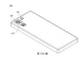
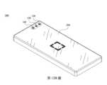
請參照第12A圖、第12B圖及第12C圖,其中第12A圖繪示依照本揭示內容第六實施例的一種電子裝置200的一側的示意圖,第12B圖繪示依照第12A圖中電子裝置200的另一側的示意圖,第12C圖繪示依照第12A圖中電子裝置200的系統示意圖。由第12A圖、第12B圖及第12C圖可知,第六實施例的電子裝置200係一智慧型手機,電子裝置200包含取像裝置100、110、120、130、140、閃光燈模組201、對焦輔助模組202、影像訊號處理器203 (Image Signal Processor; ISP)、使用者介面204以及影像軟體處理器205,其中取像裝置120、130、140為前置鏡頭。當使用者透過使用者介面204對被攝物206進行拍攝,電子裝置200利用取像裝置100、110、120、130、140聚光取像,啟動閃光燈模組201進行補光,並使用對焦輔助模組202提供的被攝物物距資訊進行快速對焦,再加上影像訊號處理器203以及影像軟體處理器205進行影像最佳化處理,來進一步提升影像鏡頭所產生的影像品質。對焦輔助模組202可採用紅外線或雷射對焦輔助系統來達到快速對焦,使用者介面204可採用觸控螢幕或實體拍攝按鈕,配合影像處理軟體的多樣化功能進行影像拍攝以及影像處理。Please refer to Figures 12A, 12B and 12C, wherein Figure 12A shows a schematic diagram of one side of an
第六實施例中的取像裝置100、110、120、130、140中至少一者可包含本揭示內容的光學鏡頭組,且可與前述第五實施例中的取像裝置100相同或具有類似的結構,在此不另贅述。詳細來說,第六實施例中的取像裝置100、110可分別為廣角取像裝置與超廣角取像裝置,亦可分別為廣角取像裝置與望遠取像裝置,而取像裝置120、130、140可分別為廣角取像裝置、超廣角取像裝置以及TOF模組 (Time-Of-Flight;飛時測距模組),但並不以此配置為限。另外,取像裝置110、120、130、140與其他構件的連接關係皆可與第11圖中繪示的取像裝置100相同,或依照取像裝置的類型適應性調整,在此不另繪示及詳述。At least one of the
<第七實施例><Seventh Embodiment>
請參照第13圖,其繪示依照本揭示內容第七實施例的一種電子裝置300的一側的示意圖。第七實施例的電子裝置300係一智慧型手機,電子裝置300包含取像裝置310、320、330以及閃光燈模組301。Please refer to FIG. 13 , which is a schematic diagram of a side of an
第七實施例的電子裝置300可包含與前述第六實施例中相同或相似的元件,且取像裝置310、320、330與其他元件的連接關係也可與第六實施例所揭露的相同或相似,在此不另贅述。第七實施例中的取像裝置310、320、330皆可包含本揭示內容的光學鏡頭組,且皆可與前述第五實施例中的取像裝置100相同或具有類似的結構,在此不另贅述。詳細來說,取像裝置310可為超廣角取像裝置,取像裝置320可為廣角取像裝置,取像裝置330可為望遠取像裝置 (可包含光路轉折元件),或另可為其他種類的取像裝置,並不限於此配置方式。The
<第八實施例><Eighth Embodiment>
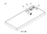
請參照第14圖,其繪示依照本揭示內容第八實施例的一種電子裝置400的一側的示意圖。第八實施例的電子裝置400係一智慧型手機,電子裝置400包含取像裝置410、420、430、440、450、460、470、480、490以及閃光燈模組401。Please refer to FIG. 14 , which shows a schematic diagram of one side of an
第八實施例的電子裝置400可包含與前述第六實施例中相同或相似的元件,且取像裝置410、420、430、440、450、460、470、480、490以及閃光燈模組401與其他元件的連接關係也可與第六實施例所揭露的相同或相似,在此不另贅述。第八實施例中的取像裝置410、420、430、440、450、460、470、480、490皆可包含本揭示內容的光學鏡頭組,且皆可與前述第五實施例中的取像裝置100相同或具有類似的結構,在此不另贅述。The
詳細來說,取像裝置410、420可分別為超廣角取像裝置,取像裝置430、440可分別為廣角取像裝置,取像裝置450、460可分別為望遠取像裝置,取像裝置470、480可分別為望遠取像裝置 (可包含光路轉折元件),取像裝置490可為TOF模組,或另可為其他種類的取像裝置,並不限於此配置方式。In detail,
<第九實施例><Ninth Embodiment>
請參照第15A圖以及第15B圖,其中第15A圖繪示依照本揭示內容第九實施例的一種電子裝置500的一側的示意圖,第15B圖繪示依照第15A圖中電子裝置500的另一側的示意圖。由第15A圖以及第15B圖可知,第九實施例的電子裝置500係一智慧型手機,電子裝置500包含取像裝置510、520、530、540以及使用者介面504。Please refer to FIG. 15A and FIG. 15B, wherein FIG. 15A is a schematic diagram of one side of an
第九實施例的電子裝置500可包含與前述第六實施例中相同或相似的元件,且取像裝置510、520、530、540以及使用者介面504與其他元件的連接關係也可與第六實施例所揭露的相同或相似,在此不另贅述。詳細來說,取像裝置510可對應電子裝置外側的一非圓形開口進行取像,取像裝置520、530、540則分別為望遠取像裝置、廣角取像裝置以及超廣角取像裝置,或另可為其他種類的取像裝置,並不限於此配置方式。The
雖然本揭示內容已以實施方式揭露如上,然其並非用以限定本揭示內容,任何熟習此技藝者,在不脫離本揭示內容的精神和範圍內,當可作各種的更動與潤飾,因此本揭示內容的保護範圍當視後附的申請專利範圍所界定者為準。Although the contents of this disclosure have been disclosed in the form of implementation as above, it is not intended to limit the contents of this disclosure. Anyone skilled in the art can make various changes and modifications without departing from the spirit and scope of the contents of this disclosure. Therefore, the protection scope of the contents of this disclosure shall be subject to the scope defined by the attached patent application.
100,110,120,130,140,310,320,330,410,420,430,440,450,460,470,480,490,510,520,530,540:取像裝置 200,300,400,500:電子裝置 101:光學鏡頭組 102:驅動裝置組 103:電子感光元件 104:影像穩定模組 201,301,401:閃光燈模組 202:對焦輔助模組 203:影像訊號處理器 204,504:使用者介面 205:影像軟體處理器 206:被攝物 OA1:第一光軸 OA2:第二光軸 OA3:第三光軸 LF,LF1,LF2:光路轉折元件 LG:透鏡群 IMG:成像面 FL:濾光元件 DC:奈米結晶顆粒的平均粒徑 Tc:奈米結晶顆粒的高度 R40100:具低反射層的表面於波長400 nm - 1000 nm的反射率 R70100:具低反射層的表面於波長700 nm - 1000 nm的反射率 R80100:具低反射層的表面於波長800 nm - 1000 nm的反射率 R90100:具低反射層的表面於波長900 nm - 1000 nm的反射率 R4060:具低反射層的表面於波長400 nm - 600 nm的反射率 R4070:具低反射層的表面於波長400 nm - 700 nm的反射率 R5060:具低反射層的表面於波長500 nm - 600 nm的反射率 R5070:具低反射層的表面於波長500 nm - 700 nm的反射率100,110,120,130,140,310,320,330,410,420,430,440,450,460,470,480,490,510,520,530,540: Image acquisition device200,300,400,500: Electronic device101: Optical lens assembly102: Drive assembly103: Electronic photosensitive element104: Image stabilization module201,301,401: Flash module202: Focus assist module203: Image signal processor204,504: User interface205: Image software processor206: ObjectOA1: First optical axisOA2: Second optical axisOA3: Third optical axisLF, LF1, LF2: Light path bending elementLG: Lens groupIMG: Imaging surfaceFL: Filter elementDC: Average particle size of nanocrystalline particlesTc: Height of nanocrystalline particlesR40100: Reflectivity of the surface with low reflection layer at wavelength 400 nm - 1000 nmR70100: Reflectivity of the surface with low reflection layer at wavelength 700 nm - 1000 nmR80100: Reflectivity of the surface with low reflection layer at wavelength 800 nm - 1000 nmR90100: Reflectivity of the surface with low reflection layer at wavelength 900 nm - 1000 nmR4060: Reflectivity of a surface with a low reflective layer at a wavelength of 400 nm - 600 nmR4070: Reflectivity of a surface with a low reflective layer at a wavelength of 400 nm - 700 nmR5060: Reflectivity of a surface with a low reflective layer at a wavelength of 500 nm - 600 nmR5070: Reflectivity of a surface with a low reflective layer at a wavelength of 500 nm - 700 nm
為讓本揭示內容的上述和其他目的、特徵、優點與實施例能更明顯易懂,所附圖式的說明如下: 第1圖係第一比較例之基底表面的影像; 第2圖係繪示第一比較例中具反射層的表面之反射率與波長的關係圖; 第3圖係繪示第二比較例中具反射層的表面之反射率與波長的關係圖; 第4圖係第一實施例之基底表面的影像; 第5圖係繪示第一實施例中具低反射層的表面之反射率與波長的關係圖; 第6圖係第二實施例的結晶表面影像; 第7圖係繪示第二實施例中具低反射層的表面之反射率與波長的關係圖; 第8圖係繪示第三實施例中具低反射層的表面之反射率與波長的關係圖; 第9圖係第四實施例的結晶表面影像; 第10圖係繪示第四實施例中具低反射層的表面之反射率與波長的關係圖; 第11圖繪示依照本揭示內容第五實施例的一種取像裝置的立體示意圖; 第12A圖繪示依照本揭示內容第六實施例的一種電子裝置的一側的示意圖; 第12B圖繪示依照第12A圖中電子裝置的另一側的示意圖; 第12C圖繪示依照第12A圖中電子裝置的系統示意圖; 第13圖繪示依照本揭示內容第七實施例的一種電子裝置的一側的示意圖; 第14圖繪示依照本揭示內容第八實施例的一種電子裝置的一側的示意圖; 第15A圖繪示依照本揭示內容第九實施例的一種電子裝置的一側的示意圖; 第15B圖繪示依照第15A圖中電子裝置的另一側的示意圖; 第16A圖繪示依照本揭示內容的光路轉折元件在光學鏡頭組中的一種配置關係示意圖; 第16B圖繪示依照本揭示內容的光路轉折元件在光學鏡頭組中的另一種配置關係示意圖; 第16C圖繪示依照本揭示內容的二光路轉折元件在光學鏡頭組中的一種配置關係示意圖; 第16D圖繪示依照本揭示內容的二光路轉折元件在光學鏡頭組中的另一種配置關係示意圖;以及 第16E圖繪示依照本揭示內容的光路轉折元件在光學鏡頭組中的又一種配置關係示意圖。In order to make the above and other purposes, features, advantages and embodiments of the present disclosure more clearly understandable, the attached drawings are described as follows: Figure 1 is an image of the substrate surface of the first comparative example; Figure 2 is a graph showing the relationship between the reflectivity and wavelength of the surface with a reflective layer in the first comparative example; Figure 3 is a graph showing the relationship between the reflectivity and wavelength of the surface with a reflective layer in the second comparative example; Figure 4 is an image of the substrate surface of the first embodiment; Figure 5 is a graph showing the relationship between the reflectivity and wavelength of the surface with a low reflective layer in the first embodiment; Figure 6 is an image of the crystal surface of the second embodiment; Figure 7 is a graph showing the relationship between the reflectivity and wavelength of the surface with a low reflective layer in the second embodiment; Figure 8 is a graph showing the relationship between the reflectivity and wavelength of the surface with a low reflective layer in the third embodiment; Figure 9 is a crystal surface image of the fourth embodiment;Figure 10 is a graph showing the relationship between the reflectivity and wavelength of the surface with a low reflection layer in the fourth embodiment;Figure 11 is a three-dimensional schematic diagram of an imaging device according to the fifth embodiment of the present disclosure;Figure 12A is a schematic diagram of one side of an electronic device according to the sixth embodiment of the present disclosure;Figure 12B is a schematic diagram of the other side of the electronic device in Figure 12A;Figure 12C is a system schematic diagram of the electronic device in Figure 12A;Figure 13 is a schematic diagram of one side of an electronic device according to the seventh embodiment of the present disclosure;Figure 14 is a schematic diagram of one side of an electronic device according to the eighth embodiment of the present disclosure;FIG. 15A is a schematic diagram of one side of an electronic device according to the ninth embodiment of the present disclosure;FIG. 15B is a schematic diagram of the other side of the electronic device in FIG. 15A;FIG. 16A is a schematic diagram of a configuration relationship of an optical path bending element in an optical lens group according to the present disclosure;FIG. 16B is a schematic diagram of another configuration relationship of an optical path bending element in an optical lens group according to the present disclosure;FIG. 16C is a schematic diagram of a configuration relationship of two optical path bending elements in an optical lens group according to the present disclosure;FIG. 16D is a schematic diagram of another configuration relationship of two optical path bending elements in an optical lens group according to the present disclosure; andFIG. 16E is a schematic diagram of another configuration relationship of an optical path bending element in an optical lens group according to the present disclosure.
Claims (27)
Translated fromChineseApplications Claiming Priority (2)
| Application Number | Priority Date | Filing Date | Title |
|---|---|---|---|
| US202263322667P | 2022-03-23 | 2022-03-23 | |
| US63/322,667 | 2022-03-23 |
Publications (2)
| Publication Number | Publication Date |
|---|---|
| TW202338404A TW202338404A (en) | 2023-10-01 |
| TWI874937Btrue TWI874937B (en) | 2025-03-01 |
Family
ID=85724753
Family Applications (2)
| Application Number | Title | Priority Date | Filing Date |
|---|---|---|---|
| TW112110718ATWI874937B (en) | 2022-03-23 | 2023-03-22 | Low reflection layer, optical lens assembly, imaging apparatus and electronic device |
| TW114102101ATW202518062A (en) | 2022-03-23 | 2023-03-22 | Optical lens assembly, imaging apparatus and electronic device |
Family Applications After (1)
| Application Number | Title | Priority Date | Filing Date |
|---|---|---|---|
| TW114102101ATW202518062A (en) | 2022-03-23 | 2023-03-22 | Optical lens assembly, imaging apparatus and electronic device |
Country Status (5)
| Country | Link |
|---|---|
| US (1) | US20230305200A1 (en) |
| EP (1) | EP4249966A1 (en) |
| CN (1) | CN116804775A (en) |
| BR (1) | BR102023005283A2 (en) |
| TW (2) | TWI874937B (en) |
Families Citing this family (1)
| Publication number | Priority date | Publication date | Assignee | Title |
|---|---|---|---|---|
| CN120195831A (en)* | 2023-12-21 | 2025-06-24 | 大立光电股份有限公司 | Imaging lens module, camera module and electronic device |
Citations (6)
| Publication number | Priority date | Publication date | Assignee | Title |
|---|---|---|---|---|
| US6773801B2 (en)* | 2001-04-06 | 2004-08-10 | Dai Nippon Printing Co., Ltd. | Fine particle layer laminated film and optical functional material |
| TW200628524A (en)* | 2004-12-21 | 2006-08-16 | Du Pont | Process for forming a patterned fluoropolymer film on a substrate |
| TW200712545A (en)* | 2005-09-20 | 2007-04-01 | Eastman Kodak Co | Nano-structured thin film with reduced light reflection |
| US20120009429A1 (en)* | 2009-01-12 | 2012-01-12 | Cleansun Energy Ltd. | substrate having a self cleaning anti-reflecting coating and method for its preparation |
| US10473823B2 (en)* | 2012-07-04 | 2019-11-12 | Canon Kabushiki Kaisha | Fine structure, optical member, antireflection film, water-repellent film, substrate for mass spectrometry, phase plate, process for producing fine structure, and process for producing antireflection film |
| TW202022472A (en)* | 2018-11-30 | 2020-06-16 | 大立光電股份有限公司 | Miniature optical lens assembly, imaging apparatus and electronic device |
Family Cites Families (8)
| Publication number | Priority date | Publication date | Assignee | Title |
|---|---|---|---|---|
| JPH07104102A (en)* | 1993-09-30 | 1995-04-21 | Olympus Optical Co Ltd | Water repellant reflection preventive film for glass-made optical parts and production thereof |
| FR2858420B1 (en)* | 2003-07-29 | 2005-11-25 | Essilor Int | OPTICAL ARTICLE COMPRISING A MULTILAYER ANTI-REFLECTING STACK AND METHOD FOR PREPARING THE SAME |
| US20070104922A1 (en)* | 2005-11-08 | 2007-05-10 | Lei Zhai | Superhydrophilic coatings |
| DE102010048088A1 (en)* | 2010-10-01 | 2012-04-05 | Carl Zeiss Vision Gmbh | Optical lens with scratch-resistant anti-reflection coating |
| JP2013152425A (en)* | 2011-12-28 | 2013-08-08 | Tamron Co Ltd | Antireflection film and optical element |
| GB201515271D0 (en)* | 2015-08-27 | 2015-10-14 | Surrey Nanosystems Ltd | Ultra low reflectivity coating and method therefor |
| CN105565678B (en)* | 2015-10-15 | 2018-04-24 | 北京科技大学 | A kind of super-hydrophobic automatic cleaning SiO of anti-reflection2Nano coating |
| CN111208588B (en)* | 2020-01-15 | 2021-08-31 | 深圳中天银河科技有限公司 | Self-dedusting monitoring camera lens and preparation method thereof |
- 2023
- 2023-03-22TWTW112110718Apatent/TWI874937B/enactive
- 2023-03-22BRBR102023005283-5Apatent/BR102023005283A2/enunknown
- 2023-03-22USUS18/187,744patent/US20230305200A1/enactivePending
- 2023-03-22CNCN202310281872.9Apatent/CN116804775A/enactivePending
- 2023-03-22EPEP23163345.4Apatent/EP4249966A1/enactivePending
- 2023-03-22TWTW114102101Apatent/TW202518062A/enunknown
Patent Citations (6)
| Publication number | Priority date | Publication date | Assignee | Title |
|---|---|---|---|---|
| US6773801B2 (en)* | 2001-04-06 | 2004-08-10 | Dai Nippon Printing Co., Ltd. | Fine particle layer laminated film and optical functional material |
| TW200628524A (en)* | 2004-12-21 | 2006-08-16 | Du Pont | Process for forming a patterned fluoropolymer film on a substrate |
| TW200712545A (en)* | 2005-09-20 | 2007-04-01 | Eastman Kodak Co | Nano-structured thin film with reduced light reflection |
| US20120009429A1 (en)* | 2009-01-12 | 2012-01-12 | Cleansun Energy Ltd. | substrate having a self cleaning anti-reflecting coating and method for its preparation |
| US10473823B2 (en)* | 2012-07-04 | 2019-11-12 | Canon Kabushiki Kaisha | Fine structure, optical member, antireflection film, water-repellent film, substrate for mass spectrometry, phase plate, process for producing fine structure, and process for producing antireflection film |
| TW202022472A (en)* | 2018-11-30 | 2020-06-16 | 大立光電股份有限公司 | Miniature optical lens assembly, imaging apparatus and electronic device |
Also Published As
| Publication number | Publication date |
|---|---|
| US20230305200A1 (en) | 2023-09-28 |
| TW202338404A (en) | 2023-10-01 |
| TW202518062A (en) | 2025-05-01 |
| EP4249966A1 (en) | 2023-09-27 |
| CN116804775A (en) | 2023-09-26 |
| BR102023005283A2 (en) | 2023-10-10 |
Similar Documents
| Publication | Publication Date | Title |
|---|---|---|
| TWI707169B (en) | Imaging lens assembly, camera module and electronic device | |
| CN114647021B (en) | Miniature optical lens, imaging device and electronic device | |
| TW202403426A (en) | Imaging lens and electronic device | |
| TWI874937B (en) | Low reflection layer, optical lens assembly, imaging apparatus and electronic device | |
| JP2013114235A (en) | Optical element, method for manufacturing optical element, optical system, and optical apparatus | |
| JP2019039961A (en) | Optical system including anti-reflection film and optical device | |
| US20240118462A1 (en) | Bokeh filter membrane, imaging optical lens assembly, imaging apparatus and electronic device | |
| JP7385364B2 (en) | Optical member, method for manufacturing optical member, optical device, and imaging device | |
| US12379524B2 (en) | Optical imaging lens assembly comprising a gradient refractive coating having a plurality of holes, imaging apparatus and electronic device | |
| TWI777542B (en) | Imaging lens assembly and electronic device | |
| TWI866863B (en) | Optical imaging lens assembly, imaging apparatus and electronic device | |
| JP7378924B2 (en) | Optical elements, their manufacturing methods, imaging devices, and optical instruments | |
| TWI862459B (en) | Catadioptric optical membrane, imaging optical lens assembly, imaging apparatus and electronic device | |
| TWI847291B (en) | Catadioptric optical membrane, imaging optical lens assembly, imaging apparatus and electronic device | |
| TWI857814B (en) | Optical lens assembly, imaging apparatus and electronic device | |
| US20240393502A1 (en) | Optical element, optical system, image pickup apparatus, and manufacturing method of an optical element | |
| TWI417643B (en) | Shutter and camera module having same |