TWI870393B - Semiconductor device and method for fabricating the same - Google Patents
Semiconductor device and method for fabricating the sameDownload PDFInfo
- Publication number
- TWI870393B TWI870393BTW109108803ATW109108803ATWI870393BTW I870393 BTWI870393 BTW I870393BTW 109108803 ATW109108803 ATW 109108803ATW 109108803 ATW109108803 ATW 109108803ATW I870393 BTWI870393 BTW I870393B
- Authority
- TW
- Taiwan
- Prior art keywords
- gate structure
- dielectric layer
- substrate
- source
- oxide semiconductor
- Prior art date
Links
Images
Classifications
- H—ELECTRICITY
- H10—SEMICONDUCTOR DEVICES; ELECTRIC SOLID-STATE DEVICES NOT OTHERWISE PROVIDED FOR
- H10D—INORGANIC ELECTRIC SEMICONDUCTOR DEVICES
- H10D88/00—Three-dimensional [3D] integrated devices
- H—ELECTRICITY
- H01—ELECTRIC ELEMENTS
- H01L—SEMICONDUCTOR DEVICES NOT COVERED BY CLASS H10
- H01L23/00—Details of semiconductor or other solid state devices
- H01L23/52—Arrangements for conducting electric current within the device in operation from one component to another, i.e. interconnections, e.g. wires, lead frames
- H01L23/535—Arrangements for conducting electric current within the device in operation from one component to another, i.e. interconnections, e.g. wires, lead frames including internal interconnections, e.g. cross-under constructions
- H—ELECTRICITY
- H01—ELECTRIC ELEMENTS
- H01L—SEMICONDUCTOR DEVICES NOT COVERED BY CLASS H10
- H01L24/00—Arrangements for connecting or disconnecting semiconductor or solid-state bodies; Methods or apparatus related thereto
- H01L24/01—Means for bonding being attached to, or being formed on, the surface to be connected, e.g. chip-to-package, die-attach, "first-level" interconnects; Manufacturing methods related thereto
- H01L24/02—Bonding areas ; Manufacturing methods related thereto
- H01L24/07—Structure, shape, material or disposition of the bonding areas after the connecting process
- H01L24/08—Structure, shape, material or disposition of the bonding areas after the connecting process of an individual bonding area
- H—ELECTRICITY
- H01—ELECTRIC ELEMENTS
- H01L—SEMICONDUCTOR DEVICES NOT COVERED BY CLASS H10
- H01L24/00—Arrangements for connecting or disconnecting semiconductor or solid-state bodies; Methods or apparatus related thereto
- H01L24/80—Methods for connecting semiconductor or other solid state bodies using means for bonding being attached to, or being formed on, the surface to be connected
- H—ELECTRICITY
- H01—ELECTRIC ELEMENTS
- H01L—SEMICONDUCTOR DEVICES NOT COVERED BY CLASS H10
- H01L25/00—Assemblies consisting of a plurality of semiconductor or other solid state devices
- H01L25/03—Assemblies consisting of a plurality of semiconductor or other solid state devices all the devices being of a type provided for in a single subclass of subclasses H10B, H10D, H10F, H10H, H10K or H10N, e.g. assemblies of rectifier diodes
- H01L25/04—Assemblies consisting of a plurality of semiconductor or other solid state devices all the devices being of a type provided for in a single subclass of subclasses H10B, H10D, H10F, H10H, H10K or H10N, e.g. assemblies of rectifier diodes the devices not having separate containers
- H01L25/065—Assemblies consisting of a plurality of semiconductor or other solid state devices all the devices being of a type provided for in a single subclass of subclasses H10B, H10D, H10F, H10H, H10K or H10N, e.g. assemblies of rectifier diodes the devices not having separate containers the devices being of a type provided for in group H10D89/00
- H01L25/0657—Stacked arrangements of devices
- H—ELECTRICITY
- H01—ELECTRIC ELEMENTS
- H01L—SEMICONDUCTOR DEVICES NOT COVERED BY CLASS H10
- H01L25/00—Assemblies consisting of a plurality of semiconductor or other solid state devices
- H01L25/50—Multistep manufacturing processes of assemblies consisting of devices, the devices being individual devices of subclass H10D or integrated devices of class H10
- H—ELECTRICITY
- H10—SEMICONDUCTOR DEVICES; ELECTRIC SOLID-STATE DEVICES NOT OTHERWISE PROVIDED FOR
- H10B—ELECTRONIC MEMORY DEVICES
- H10B10/00—Static random access memory [SRAM] devices
- H10B10/12—Static random access memory [SRAM] devices comprising a MOSFET load element
- H—ELECTRICITY
- H10—SEMICONDUCTOR DEVICES; ELECTRIC SOLID-STATE DEVICES NOT OTHERWISE PROVIDED FOR
- H10D—INORGANIC ELECTRIC SEMICONDUCTOR DEVICES
- H10D84/00—Integrated devices formed in or on semiconductor substrates that comprise only semiconducting layers, e.g. on Si wafers or on GaAs-on-Si wafers
- H10D84/01—Manufacture or treatment
- H10D84/0123—Integrating together multiple components covered by H10D12/00 or H10D30/00, e.g. integrating multiple IGBTs
- H10D84/0126—Integrating together multiple components covered by H10D12/00 or H10D30/00, e.g. integrating multiple IGBTs the components including insulated gates, e.g. IGFETs
- H10D84/0149—Manufacturing their interconnections or electrodes, e.g. source or drain electrodes
- H—ELECTRICITY
- H10—SEMICONDUCTOR DEVICES; ELECTRIC SOLID-STATE DEVICES NOT OTHERWISE PROVIDED FOR
- H10D—INORGANIC ELECTRIC SEMICONDUCTOR DEVICES
- H10D84/00—Integrated devices formed in or on semiconductor substrates that comprise only semiconducting layers, e.g. on Si wafers or on GaAs-on-Si wafers
- H10D84/01—Manufacture or treatment
- H10D84/02—Manufacture or treatment characterised by using material-based technologies
- H10D84/03—Manufacture or treatment characterised by using material-based technologies using Group IV technology, e.g. silicon technology or silicon-carbide [SiC] technology
- H10D84/038—Manufacture or treatment characterised by using material-based technologies using Group IV technology, e.g. silicon technology or silicon-carbide [SiC] technology using silicon technology, e.g. SiGe
- H—ELECTRICITY
- H10—SEMICONDUCTOR DEVICES; ELECTRIC SOLID-STATE DEVICES NOT OTHERWISE PROVIDED FOR
- H10D—INORGANIC ELECTRIC SEMICONDUCTOR DEVICES
- H10D88/00—Three-dimensional [3D] integrated devices
- H10D88/01—Manufacture or treatment
- H—ELECTRICITY
- H10—SEMICONDUCTOR DEVICES; ELECTRIC SOLID-STATE DEVICES NOT OTHERWISE PROVIDED FOR
- H10D—INORGANIC ELECTRIC SEMICONDUCTOR DEVICES
- H10D89/00—Aspects of integrated devices not covered by groups H10D84/00 - H10D88/00
- H10D89/10—Integrated device layouts
- H—ELECTRICITY
- H01—ELECTRIC ELEMENTS
- H01L—SEMICONDUCTOR DEVICES NOT COVERED BY CLASS H10
- H01L2224/00—Indexing scheme for arrangements for connecting or disconnecting semiconductor or solid-state bodies and methods related thereto as covered by H01L24/00
- H01L2224/01—Means for bonding being attached to, or being formed on, the surface to be connected, e.g. chip-to-package, die-attach, "first-level" interconnects; Manufacturing methods related thereto
- H01L2224/02—Bonding areas; Manufacturing methods related thereto
- H01L2224/07—Structure, shape, material or disposition of the bonding areas after the connecting process
- H01L2224/08—Structure, shape, material or disposition of the bonding areas after the connecting process of an individual bonding area
- H01L2224/081—Disposition
- H01L2224/0812—Disposition the bonding area connecting directly to another bonding area, i.e. connectorless bonding, e.g. bumpless bonding
- H01L2224/08135—Disposition the bonding area connecting directly to another bonding area, i.e. connectorless bonding, e.g. bumpless bonding the bonding area connecting between different semiconductor or solid-state bodies, i.e. chip-to-chip
- H01L2224/08145—Disposition the bonding area connecting directly to another bonding area, i.e. connectorless bonding, e.g. bumpless bonding the bonding area connecting between different semiconductor or solid-state bodies, i.e. chip-to-chip the bodies being stacked
- H—ELECTRICITY
- H01—ELECTRIC ELEMENTS
- H01L—SEMICONDUCTOR DEVICES NOT COVERED BY CLASS H10
- H01L2224/00—Indexing scheme for arrangements for connecting or disconnecting semiconductor or solid-state bodies and methods related thereto as covered by H01L24/00
- H01L2224/01—Means for bonding being attached to, or being formed on, the surface to be connected, e.g. chip-to-package, die-attach, "first-level" interconnects; Manufacturing methods related thereto
- H01L2224/10—Bump connectors; Manufacturing methods related thereto
- H01L2224/15—Structure, shape, material or disposition of the bump connectors after the connecting process
- H01L2224/16—Structure, shape, material or disposition of the bump connectors after the connecting process of an individual bump connector
- H01L2224/161—Disposition
- H01L2224/16135—Disposition the bump connector connecting between different semiconductor or solid-state bodies, i.e. chip-to-chip
- H01L2224/16145—Disposition the bump connector connecting between different semiconductor or solid-state bodies, i.e. chip-to-chip the bodies being stacked
- H—ELECTRICITY
- H01—ELECTRIC ELEMENTS
- H01L—SEMICONDUCTOR DEVICES NOT COVERED BY CLASS H10
- H01L2224/00—Indexing scheme for arrangements for connecting or disconnecting semiconductor or solid-state bodies and methods related thereto as covered by H01L24/00
- H01L2224/80—Methods for connecting semiconductor or other solid state bodies using means for bonding being attached to, or being formed on, the surface to be connected
- H01L2224/80001—Methods for connecting semiconductor or other solid state bodies using means for bonding being attached to, or being formed on, the surface to be connected by connecting a bonding area directly to another bonding area, i.e. connectorless bonding, e.g. bumpless bonding
- H01L2224/808—Bonding techniques
- H01L2224/80894—Direct bonding, i.e. joining surfaces by means of intermolecular attracting interactions at their interfaces, e.g. covalent bonds, van der Waals forces
- H01L2224/80895—Direct bonding, i.e. joining surfaces by means of intermolecular attracting interactions at their interfaces, e.g. covalent bonds, van der Waals forces between electrically conductive surfaces, e.g. copper-copper direct bonding, surface activated bonding
- H—ELECTRICITY
- H01—ELECTRIC ELEMENTS
- H01L—SEMICONDUCTOR DEVICES NOT COVERED BY CLASS H10
- H01L2224/00—Indexing scheme for arrangements for connecting or disconnecting semiconductor or solid-state bodies and methods related thereto as covered by H01L24/00
- H01L2224/80—Methods for connecting semiconductor or other solid state bodies using means for bonding being attached to, or being formed on, the surface to be connected
- H01L2224/80001—Methods for connecting semiconductor or other solid state bodies using means for bonding being attached to, or being formed on, the surface to be connected by connecting a bonding area directly to another bonding area, i.e. connectorless bonding, e.g. bumpless bonding
- H01L2224/808—Bonding techniques
- H01L2224/80894—Direct bonding, i.e. joining surfaces by means of intermolecular attracting interactions at their interfaces, e.g. covalent bonds, van der Waals forces
- H01L2224/80896—Direct bonding, i.e. joining surfaces by means of intermolecular attracting interactions at their interfaces, e.g. covalent bonds, van der Waals forces between electrically insulating surfaces, e.g. oxide or nitride layers
- H—ELECTRICITY
- H01—ELECTRIC ELEMENTS
- H01L—SEMICONDUCTOR DEVICES NOT COVERED BY CLASS H10
- H01L2225/00—Details relating to assemblies covered by the group H01L25/00 but not provided for in its subgroups
- H01L2225/03—All the devices being of a type provided for in the same main group of the same subclass of class H10, e.g. assemblies of rectifier diodes
- H01L2225/04—All the devices being of a type provided for in the same main group of the same subclass of class H10, e.g. assemblies of rectifier diodes the devices not having separate containers
- H01L2225/065—All the devices being of a type provided for in the same main group of the same subclass of class H10
- H01L2225/06503—Stacked arrangements of devices
- H01L2225/0652—Bump or bump-like direct electrical connections from substrate to substrate
- H—ELECTRICITY
- H01—ELECTRIC ELEMENTS
- H01L—SEMICONDUCTOR DEVICES NOT COVERED BY CLASS H10
- H01L2225/00—Details relating to assemblies covered by the group H01L25/00 but not provided for in its subgroups
- H01L2225/03—All the devices being of a type provided for in the same main group of the same subclass of class H10, e.g. assemblies of rectifier diodes
- H01L2225/04—All the devices being of a type provided for in the same main group of the same subclass of class H10, e.g. assemblies of rectifier diodes the devices not having separate containers
- H01L2225/065—All the devices being of a type provided for in the same main group of the same subclass of class H10
- H01L2225/06503—Stacked arrangements of devices
- H01L2225/06524—Electrical connections formed on device or on substrate, e.g. a deposited or grown layer
- H—ELECTRICITY
- H01—ELECTRIC ELEMENTS
- H01L—SEMICONDUCTOR DEVICES NOT COVERED BY CLASS H10
- H01L2225/00—Details relating to assemblies covered by the group H01L25/00 but not provided for in its subgroups
- H01L2225/03—All the devices being of a type provided for in the same main group of the same subclass of class H10, e.g. assemblies of rectifier diodes
- H01L2225/04—All the devices being of a type provided for in the same main group of the same subclass of class H10, e.g. assemblies of rectifier diodes the devices not having separate containers
- H01L2225/065—All the devices being of a type provided for in the same main group of the same subclass of class H10
- H01L2225/06503—Stacked arrangements of devices
- H01L2225/06541—Conductive via connections through the device, e.g. vertical interconnects, through silicon via [TSV]
- H—ELECTRICITY
- H01—ELECTRIC ELEMENTS
- H01L—SEMICONDUCTOR DEVICES NOT COVERED BY CLASS H10
- H01L24/00—Arrangements for connecting or disconnecting semiconductor or solid-state bodies; Methods or apparatus related thereto
- H01L24/01—Means for bonding being attached to, or being formed on, the surface to be connected, e.g. chip-to-package, die-attach, "first-level" interconnects; Manufacturing methods related thereto
- H01L24/10—Bump connectors ; Manufacturing methods related thereto
- H01L24/15—Structure, shape, material or disposition of the bump connectors after the connecting process
- H01L24/16—Structure, shape, material or disposition of the bump connectors after the connecting process of an individual bump connector
- H—ELECTRICITY
- H01—ELECTRIC ELEMENTS
- H01L—SEMICONDUCTOR DEVICES NOT COVERED BY CLASS H10
- H01L2924/00—Indexing scheme for arrangements or methods for connecting or disconnecting semiconductor or solid-state bodies as covered by H01L24/00
- H01L2924/10—Details of semiconductor or other solid state devices to be connected
- H01L2924/11—Device type
- H01L2924/14—Integrated circuits
- H01L2924/143—Digital devices
- H01L2924/1431—Logic devices
- H—ELECTRICITY
- H01—ELECTRIC ELEMENTS
- H01L—SEMICONDUCTOR DEVICES NOT COVERED BY CLASS H10
- H01L2924/00—Indexing scheme for arrangements or methods for connecting or disconnecting semiconductor or solid-state bodies as covered by H01L24/00
- H01L2924/10—Details of semiconductor or other solid state devices to be connected
- H01L2924/11—Device type
- H01L2924/14—Integrated circuits
- H01L2924/143—Digital devices
- H01L2924/1434—Memory
- H01L2924/1435—Random access memory [RAM]
- H01L2924/1437—Static random-access memory [SRAM]
Landscapes
- Engineering & Computer Science (AREA)
- Microelectronics & Electronic Packaging (AREA)
- Power Engineering (AREA)
- Computer Hardware Design (AREA)
- Physics & Mathematics (AREA)
- Condensed Matter Physics & Semiconductors (AREA)
- General Physics & Mathematics (AREA)
- Manufacturing & Machinery (AREA)
- Semiconductor Memories (AREA)
Abstract
Description
Translated fromChinese本發明是關於一種製作半導體元件,尤指一種製作靜態隨機存取記憶體的方法。The present invention relates to a method for manufacturing a semiconductor device, and more particularly to a method for manufacturing a static random access memory.
在一嵌入式靜態隨機存取記憶體(embedded static random access memory, embedded SRAM)中,包含有邏輯電路(logic circuit)和與邏輯電路連接之靜態隨機存取記憶體。靜態隨機存取記憶體本身屬於一種揮發性(volatile)的記憶單元(memory cell),亦即當供給靜態隨機存取記憶體之電力消失之後,所儲存之資料會同時抹除。靜態隨機存取記憶體儲存資料之方式是利用記憶單元內電晶體的導電狀態來達成,靜態隨機存取記憶體的設計是採用互耦合電晶體為基礎,沒有電容器放電的問題,不需要不斷充電以保持資料不流失,也就是不需作記憶體更新的動作,這與同屬揮發性記憶體的動態隨機存取記憶體(Dynamic Random Access Memory, DRAM)利用電容器帶電狀態儲存資料的方式並不相同。靜態隨機存取記憶體之存取速度相當快,因此有在電腦系統中當作快取記憶體(cache memory)等之應用。An embedded static random access memory (embedded SRAM) includes a logic circuit and a static random access memory connected to the logic circuit. The static random access memory itself is a volatile memory cell, which means that when the power supplied to the static random access memory disappears, the stored data will be erased at the same time. Static random access memory stores data by using the conductive state of the transistors in the memory cells. The design of static random access memory is based on mutually coupled transistors. There is no problem of capacitor discharge, and it does not need to be constantly charged to keep the data from being lost. In other words, there is no need to update the memory. This is different from the dynamic random access memory (DRAM), which is also a volatile memory and uses the charged state of the capacitor to store data. The access speed of static random access memory is very fast, so it is used as cache memory in computer systems.
一般而言,現行靜態隨機存取記憶體架構在讀取速度上雖相較於習知記憶體元件快速許多但仍佔據過大面積並造成空間浪費。因此如何改善現有靜態隨機存取記憶體架構即為現今一重要課題。Generally speaking, although the current static random access memory architecture is much faster than the learning memory device in terms of read speed, it still occupies too large an area and causes space waste. Therefore, how to improve the current static random access memory architecture is an important issue today.
本發明一實施例揭露一種製作半導體元件的方法,其主要先形成第一金氧半導體電晶體於第一基底上,形成第一層間介電層並覆蓋第一金氧半導體電晶體,形成第二金氧半導體電晶體於第二基底上,形成第二層間介電層於第二金氧半導體電晶體上,然後於第二層間介電層覆蓋第二金氧半導體電晶體上之後將第二基底黏接至第一層間介電層上。An embodiment of the present invention discloses a method for manufacturing a semiconductor element, which mainly comprises first forming a first metal oxide semiconductor transistor on a first substrate, forming a first interlayer dielectric layer and covering the first metal oxide semiconductor transistor, forming a second metal oxide semiconductor transistor on a second substrate, forming a second interlayer dielectric layer on the second metal oxide semiconductor transistor, and then bonding the second substrate to the first interlayer dielectric layer after the second interlayer dielectric layer covers the second metal oxide semiconductor transistor.
本發明另一實施例揭露一種半導體元件,其主要包含第一金氧半導體電晶體設於第一基底上、第一層間介電層設於第一金氧半導體電晶體上、第二基底設於第一層間介電層上以及第二金氧半導體電晶體設於第二基底上。Another embodiment of the present invention discloses a semiconductor element, which mainly includes a first metal oxide semiconductor transistor disposed on a first substrate, a first interlayer dielectric layer disposed on the first metal oxide semiconductor transistor, a second substrate disposed on the first interlayer dielectric layer, and a second metal oxide semiconductor transistor disposed on the second substrate.
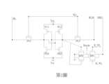
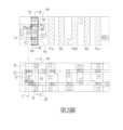
請參照第1圖與第2圖,第1圖為本發明靜態隨機存取記憶體中一組十電晶體靜態隨機存取記憶體(ten-transistor SRAM, 10T-SRAM)記憶單元之電路圖,第2圖為第1圖之靜態隨機存取記憶體之佈局圖。如第1圖與第2圖所示,本發明之靜態隨機存取記憶體較佳包含至少一組靜態隨機存取記憶體單元,其中每一靜態隨機存取記憶體單元包含一十電晶體靜態隨機存取記憶單元(10T-SRAM)。Please refer to FIG. 1 and FIG. 2. FIG. 1 is a circuit diagram of a group of ten-transistor SRAM (10T-SRAM) memory cells in the SRAM of the present invention, and FIG. 2 is a layout diagram of the SRAM of FIG. 1. As shown in FIG. 1 and FIG. 2, the SRAM of the present invention preferably includes at least one group of SRAM cells, wherein each SRAM cell includes a ten-transistor SRAM cell (10T-SRAM).
在本實施例中,10T-SRAM記憶單元較佳包含一第一上拉元件(pull-up device)PU1、一第二上拉元件PU2、一第一下拉元件(pull-down device)PD1、一第二下拉元件PD2、一第一存取元件(pass gate device)PG1、一第二存取元件PG2、二電晶體所組成的讀取端下拉元件(read port pull down device)RPD以及二電晶體所組成的讀取端存取元件(read portion pass gate device)RPG,其中第一上拉元件PU1和第二上拉元件PU2、第一下拉元件PD1和第二下拉元件PD2構成栓鎖電路(latch),使資料可以栓鎖在元件間的儲存節點(Storage Node)。另外第一上拉元件PU1和第二上拉元件PU2是作為主動負載之用,其亦可以一般之電阻來取代做為上拉元件,在此情況下即為四電晶體靜態隨機存取記憶體(four-transistor SRAM, 4T-SRAM)。另外在本實施例中,第一上拉元件PU1和第二上拉元件PU2各自之一源極區域電連接至一電壓源Vcc,第一下拉元件PD1和第二下拉元件PD2各自之一源極區域電連接至一電壓源Vss。In the present embodiment, the 10T-SRAM memory cell preferably includes a first pull-up device PU1, a second pull-up device PU2, a first pull-down device PD1, a second pull-down device PD2, a first access device PG1, a second access device PG2, a read port pull-down device RPD composed of two transistors, and a read portion pass gate device RPG composed of two transistors, wherein the first pull-up device PU1 and the second pull-up device PU2, the first pull-down device PD1 and the second pull-down device PD2 constitute a latch circuit (latch), so that data can be latched in the storage node (Storage Node) between the devices. In addition, the first pull-up element PU1 and the second pull-up element PU2 are used as active loads, and can also be replaced by ordinary resistors as pull-up elements, in this case, a four-transistor SRAM (4T-SRAM). In addition, in this embodiment, one source region of each of the first pull-up element PU1 and the second pull-up element PU2 is electrically connected to a voltage source Vcc, and one source region of each of the first pull-down element PD1 and the second pull-down element PD2 is electrically connected to a voltage source Vss.
在一實施例中,10T-SRAM記憶單元的第一上拉元件PU1、第二上拉元件PU2是由P型金氧半導體(P-type metal oxide semiconductor, PMOS)電晶體所組成,而第一下拉元件PD1、第二下拉元件PD2和第一存取元件PG1、第二存取元件PG2、讀取端下拉元件RPD以及讀取端存取元件RPG則是由N型金氧半導體(N-type metal oxide semiconductor, NMOS)電晶體所組成,但本發明不限於此。其中,第一上拉元件PU1和第一下拉元件PD1一同構成一反相器(inverter),且這兩者所構成的串接電路其兩端點分別耦接於一電壓源Vcc與一電壓源Vss;同樣地,第二上拉元件PU2與第二下拉元件PD2構成另一反相器,而這兩者所構成的串接電路其兩端點亦分別耦接於電壓源Vcc與電壓源Vss。In one embodiment, the first pull-up element PU1 and the second pull-up element PU2 of the 10T-SRAM memory cell are composed of P-type metal oxide semiconductor (PMOS) transistors, and the first pull-down element PD1, the second pull-down element PD2 and the first access element PG1, the second access element PG2, the read-end pull-down element RPD and the read-end access element RPG are composed of N-type metal oxide semiconductor (NMOS) transistors, but the present invention is not limited to this. Among them, the first pull-up element PU1 and the first pull-down element PD1 together constitute an inverter, and the two ends of the series circuit formed by the two are respectively coupled to a voltage source Vcc and a voltage source Vss; similarly, the second pull-up element PU2 and the second pull-down element PD2 constitute another inverter, and the two ends of the series circuit formed by the two are also respectively coupled to the voltage source Vcc and the voltage source Vss.
此外,第一存取元件PG1和第二存取元件PG2的閘極則分別耦接至一字元線(Word Line)WL,第一存取元件PG1的源極(Source)耦接至相對應之一位元線(Bit Line)BL,第二存取元件PG2的源極耦接至相對應之一位元線BLB,讀取端下拉元件RPD的其中一閘極藕接至第二上拉元件PU2與第二下拉元件PD2之間的節點,讀取端存取元件RPG的二閘極分別藕接至字元線R_WL,讀取端存取元件RPG的一源極藕接至位元線RBL且讀取端下拉元件RPD與讀取端存取元件RPG共同連接至一節點Rnode。In addition, the gates of the first access element PG1 and the second access element PG2 are respectively coupled to a word line WL, the source of the first access element PG1 is coupled to a corresponding bit line BL, the source of the second access element PG2 is coupled to a corresponding bit line BLB, one of the gates of the read-end pull-down element RPD is coupled to a node between the second pull-up element PU2 and the second pull-down element PD2, two gates of the read-end access element RPG are respectively coupled to the word line R_WL, a source of the read-end access element RPG is coupled to the bit line RBL, and the read-end pull-down element RPD and the read-end access element RPG are commonly connected to a node Rnode.
相較於習知6T-SRAM或8T-SRAM的記憶體架構,本實施例的10T-SRAM主要加入讀取端下拉元件RPD以及讀取端存取元件RPG等兩組元件使記憶體元件可同時進行寫入與讀取的動作。舉例來說,傳統6T-SRAM的架構下一般寫入一個訊號後需重新開啟電晶體再進行讀取,但在本實施例的10T-SRAM架構下藉由節點連接讀取端下拉元件RPD與習知6T-SRAM,在進行寫入動作時可同時經由節點將訊號傳遞出來,達到同時進行讀取與寫入的操作。Compared with the memory architecture of the conventional 6T-SRAM or 8T-SRAM, the 10T-SRAM of the present embodiment mainly adds two sets of components, namely, the read-end pull-down component RPD and the read-end access component RPG, so that the memory component can perform writing and reading operations at the same time. For example, under the conventional 6T-SRAM architecture, after writing a signal, the transistor needs to be turned on again before reading. However, under the 10T-SRAM architecture of the present embodiment, the read-end pull-down component RPD and the conventional 6T-SRAM are connected through a node, and the signal can be transmitted through the node at the same time when performing a writing operation, so as to achieve the operation of reading and writing at the same time.
需注意的是雖然10T-SRAM架構在讀取速度上相較於習知6T-SRAM或8T-SRAM快速許多,但由於佔據面積過大因此在製作上容易造成空間浪費。為了改善此缺點本發明主要將讀取端下拉元件RPD以及讀取端存取元件RPG等兩組電晶體分別設置於不同層,例如第2圖所示下半部為讀取端下拉元件RPD而上半部則為讀取端存取元件RPG,藉此節省元件空間。It should be noted that although the 10T-SRAM architecture is much faster in read speed than the conventional 6T-SRAM or 8T-SRAM, it occupies too much area and is therefore prone to waste space in manufacturing. In order to improve this shortcoming, the present invention mainly sets two sets of transistors, such as the read-end pull-down element RPD and the read-end access element RPG, on different layers. For example, as shown in FIG. 2, the lower half is the read-end pull-down element RPD and the upper half is the read-end access element RPG, thereby saving component space.
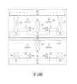
請繼續參照第3圖至第4圖,第3圖至第4圖為本發明一實施例之靜態隨機存取記憶體之結構示意圖,其中第3圖下半部為第2圖中沿著切線AA’之讀取端下拉元件RPD之結構示意圖,第3圖上半部為第2圖中沿著切線BB’之讀取端存取元件RPG之結構示意圖,而第4圖則為第2圖中沿著切線CC’由讀取端下拉元件RPD連接至讀取端存取元件RPG之結構示意圖。如第3圖至第4圖所示,首先提供一基底12,例如一由半導體材料所構成的基底12,其中半導體材料可選自由矽、鍺、矽鍺複合物、矽碳化物(silicon carbide)、砷化鎵(gallium arsenide)等所構成之群組。Please continue to refer to Figures 3 to 4, which are structural schematic diagrams of a static random access memory of an embodiment of the present invention, wherein the lower half of Figure 3 is a structural schematic diagram of the read-end pull-down element RPD along the cut line AA’ in Figure 2, the upper half of Figure 3 is a structural schematic diagram of the read-end access element RPG along the cut line BB’ in Figure 2, and Figure 4 is a structural schematic diagram of the read-end pull-down element RPD connected to the read-end access element RPG along the cut line CC’ in Figure 2. As shown in FIGS. 3 to 4 , a
然後於基底12上形成金氧半導體(metal-oxide semiconductor, MOS)電晶體14、16如讀取端下拉元件RPD等主動元件以及例如層間介電層(interlayer dielectric, ILD)28等介電層覆蓋於其上。更具體而言,基底12上可包含平面型或非平面型(如鰭狀結構電晶體)等電晶體元件,其中金氧半導體電晶體14、16可包含至少一閘極結構如閘極結構18、20設於基底12上、側壁子(圖未示)與源極/汲極區域22設於閘極結構18、20兩側的基底12內以及選擇性磊晶層與金屬矽化物設於源極/汲極區域22表面。Then, metal-oxide semiconductor (MOS)
在本實施例中,各閘極結構18、20可包含一閘極介電層24以及一閘極電極26,其中閘極介電層24較佳包含氧化矽而閘極電極26則可包含多晶矽或金屬材料。本實施例的閘極結構18、20雖以多晶矽所構成的閘極電極26為例,但不侷限於此,依據本發明其他實施例又可依據金屬閘極置換(replacement metal gate, RMG)製程將多晶矽所構成的閘極結構18、20轉換為包含功函數金屬材料的金屬閘極,此變化型也屬本發明所涵蓋的範圍。而由於依據RMG製程將多晶矽閘極轉換為金屬閘極為本領域所熟知技藝,在此不另加贅述。In this embodiment, each
另外側壁子可包含單一側壁子或複合式側壁子,例如可細部包含一偏位側壁子(圖未示)以及一主側壁子(圖未示),且側壁子可選自由氧化矽、氮化矽、氮氧化矽以及氮碳化矽所構成的群組,但不侷限於此。源極/汲極區域22與磊晶層可依據所置備電晶體的導電型式而包含不同摻質或不同材料。例如源極/汲極區域22可包含P型摻質或N型摻質,而磊晶層則可包含鍺化矽、碳化矽或磷化矽。In addition, the sidewalls may include a single sidewall or a composite sidewall, for example, a partial sidewall (not shown) and a main sidewall (not shown), and the sidewalls may be selected from a group consisting of silicon oxide, silicon nitride, silicon oxynitride, and silicon carbide nitride, but are not limited thereto. The source/
層間介電層28可設於基底12上並覆蓋各金氧半導體電晶體14、16,且層間介電層28中可設有複數個接觸插塞30、32電連接電晶體的源極/汲極區域22。然後進行一金屬內連線製程於層間介電層28上形成金屬間介電層34以及金屬內連線36、38、40鑲嵌於金屬間介電層34內並電連接接觸插塞30、32。在本實施例中接觸插塞30、32以及/或金屬內連線36、38、40均可依據單鑲嵌製程或雙鑲嵌製程鑲嵌於層間介電層28以及/或層間介電層28上的金屬間介電層34內,其中各接觸插塞30、32以及/或金屬內連線36、38、40可更細部包含一阻障層以及一金屬層,阻障層可選自由鈦(Ti)、氮化鈦(TiN)、鉭(Ta)以及氮化鉭(TaN)所構成的群組,而金屬層可選自由鎢(W)、銅(Cu)、鋁(Al)、鈦鋁合金(TiAl)、鈷鎢磷化物(cobalt tungsten phosphide,CoWP)等所構成的群組,但不侷限於此。由於平面型或非平面型電晶體與金屬內連線等相關製程均為本領域所熟知技藝,在此不另加贅述,另外在此階段即完成第2圖讀取端下拉元件RPD的製作。An interlayer
接著可重複上述形成讀取端下拉元件RPD的步驟於金屬內連線40上形成讀取端存取元件RPG。舉例來說,可先進行一磊晶成長製程於下層所製備完成的讀取端下拉元件RPD上或更具體而言金屬內連線40表面形成另一基底42例如一由半導體材料所構成的基底42,其中半導體材料可選自由矽、鍺、矽鍺複合物、矽碳化物(silicon carbide)、砷化鎵(gallium arsenide)等所構成之群組。Then, the above steps of forming the read-side pull-down device RPD may be repeated to form the read-side access device RPG on the
然後於基底42上形成金氧半導體(metal-oxide semiconductor, MOS)電晶體44、46如讀取端存取元件RPG等主動元件以及層間介電層(interlayer dielectric, ILD)58覆蓋於其上。如前所述,基底42上可包含平面型或非平面型(如鰭狀結構電晶體)等電晶體元件,其中各金氧半導體電晶體44、46可包含至少一閘極結構如閘極結構48、50設於基底42上、側壁子與源極/汲極區域52設於閘極結構48、50兩側的基底42內以及選擇性磊晶層與金屬矽化物設於源極/汲極區域52表面。Then, metal-oxide semiconductor (MOS)
如同讀取端下拉元件RPD的閘極結構18、20,讀取端存取元件RPG的閘極結構48、50可包含一閘極介電層54以及一閘極電極56,其中閘極介電層54較佳包含氧化矽而閘極電極56則可包含多晶矽或金屬材料。本實施例的閘極結構48、50雖以多晶矽所構成的閘極電極56為例,但不侷限於此,依據本發明其他實施例又可依據金屬閘極置換(replacement metal gate, RMG)製程將多晶矽所構成的閘極結構48、50轉換為包含功函數金屬材料的金屬閘極,此變化型也屬本發明所涵蓋的範圍。Like the
如同前述實施例側壁子可包含單一側壁子或複合式側壁子,例如可細部包含一偏位側壁子(圖未示)以及一主側壁子(圖未示),且側壁子可選自由氧化矽、氮化矽、氮氧化矽以及氮碳化矽所構成的群組,但不侷限於此。源極/汲極區域52與磊晶層可依據所置備電晶體的導電型式而包含不同摻質或不同材料。例如源極/汲極區域52可包含P型摻質或N型摻質,而磊晶層則可包含鍺化矽、碳化矽或磷化矽。As in the aforementioned embodiment, the sidewalls may include a single sidewall or a composite sidewall, for example, a partial sidewall (not shown) and a main sidewall (not shown), and the sidewalls may be selected from the group consisting of silicon oxide, silicon nitride, silicon oxynitride, and silicon carbonitride, but not limited thereto. The source/
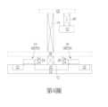
層間介電層58可設於基底42上並覆蓋各金氧半導體電晶體44、46,且層間介電層58中可設有接觸插塞或金屬內連線60、62、74電連接閘極結構48、50之間的源極/汲極區域52。需注意的是,第4圖中設於金屬內連線60旁的金屬內連線74較佳作為一橋梁同時電連接下層讀取端下拉元件RPD的源極/汲極區域22以及上層讀取端存取元件RPG的源極/汲極區域52。另外為了更簡潔顯示金屬內連線74及所連接的元件,第4圖中較佳省略設於金屬內連線74旁上層讀取端存取元件RPG的閘極結構50。An interlayer
然後進行一金屬內連線製程形成金屬間介電層64以及接觸插塞或金屬內連線66、68、70鑲嵌於金屬間介電層64內並電連接閘極結構48、50兩側的源極/汲極區域52。在本實施例中金屬內連線60、62、66、68、70可依據單鑲嵌製程或雙鑲嵌製程鑲嵌於層間介電層58內以及/或金屬間介電層64內,其中各金屬內連線60、62、66、68、70可更細部包含一阻障層以及一金屬層,阻障層可選自由鈦(Ti)、氮化鈦(TiN)、鉭(Ta)以及氮化鉭(TaN)所構成的群組,而金屬層可選自由鎢(W)、銅(Cu)、鋁(Al)、鈦鋁合金(TiAl)、鈷鎢磷化物(cobalt tungsten phosphide,CoWP)等所構成的群組,但不侷限於此。在此階段即完成第2圖讀取端存取元件RPG的製作。Then, a metal interconnection process is performed to form an intermetallic
值得注意的是,除了上述實施例以磊晶成長方式直接於下層所製備完成的讀取端下拉元件RPD上形成由半導體材料所構成的基底42後再進行讀取端存取元件RPG的製作,依據本發明另一實施例又可於讀取端下拉元件RPD製作完成後於先在另一由半導體材料所構成的基底42或矽晶圓上進行讀取端存取元件RPG的製作,迨所有元件包括閘極結構、源極/汲極區域、層間介電層、金屬間介電層以及金屬內連線等元件製作完成後再利用利用接合(bonding)技術將設有讀取端存取元件RPG的基底42黏接至讀取端下拉元件RPD上或更具體而言金屬內連線40表面,此實施例也屬本發明所涵蓋的範圍。另外在本實施例中,若下層的讀取端下拉元件RPD與上層的讀取端存取元件RPG選擇經由接合方式進行連結,則兩者之間可依據製程或產品需求利用凸塊或矽貫通電極(through-silicon via, TSV)進行訊號傳遞,這些變化型均屬本發明所涵蓋的範圍。It is worth noting that in addition to the above-mentioned embodiment of directly forming a
綜上所述,由於現行10T-SRAM架構在讀取速度上雖較習知6T-SRAM或8T-SRAM快速許多但仍佔據過大面積造成空間浪費,因此本發明主要將10T-SRAM元件中的讀取端下拉元件RPD以及讀取端存取元件RPG等兩組電晶體元件分別設置於不同層,例如第2圖及第3圖所示下層為讀取端下拉元件RPD而上層則為讀取端存取元件RPG,藉此節省元件空間。依據前述實施例,本發明可先於第一基底12上進行下層讀取端下拉元件RPD的製作後利用磊晶成長製程於讀取端下拉元件RPD的最上層金屬內連線表面形成另一由半導體材料所構成的基底42,再於其上進行讀取端存取元件RPG的製作。除此之外,本發明另一實施例又可選擇先於第一基底12上進行讀取端下拉元件RPD的製作,然後於另一同樣由半導體材料所構成的第二基底42或矽晶圓上進行讀取端存取元件RPG的製作,迨兩者均完成後再利用接合技術將承載讀取端存取元件RPG的基底42附著於讀取端下拉元件RPD的最上層金屬內連線上,這兩種變化行均屬本發明所涵蓋的範圍。 以上所述僅為本發明之較佳實施例,凡依本發明申請專利範圍所做之均等變化與修飾,皆應屬本發明之涵蓋範圍。In summary, although the current 10T-SRAM architecture is much faster than the conventional 6T-SRAM or 8T-SRAM in terms of read speed, it still occupies too large an area and causes space waste. Therefore, the present invention mainly arranges two sets of transistor elements, namely the read-end pull-down element RPD and the read-end access element RPG, in the 10T-SRAM element in different layers. For example, as shown in FIG. 2 and FIG. 3, the lower layer is the read-end pull-down element RPD and the upper layer is the read-end access element RPG, thereby saving element space. According to the above-mentioned embodiment, the present invention can firstly manufacture the lower layer read-end pull-down element RPD on the
12:基底 14:金氧半導體電晶體 16:金氧半導體電晶體 18:閘極結構 20:閘極結構 22:源極/汲極區域 24:閘極介電層 26:閘極電極 28:層間介電層 30:接觸插塞 32:接觸插塞 34:金屬間介電層 36:金屬內連線 38:金屬內連線 40:金屬內連線 42:基底 44:金氧半導體電晶體 46:金氧半導體電晶體 48:閘極結構 50:閘極結構 52:源極/汲極區域 54:閘極介電層 56:閘極電極 58:層間介電層 60:金屬內連線 62:金屬內連線 64:金屬間介電層 66:金屬內連線 68:金屬內連線 70:金屬內連線 72:接觸插塞 74:金屬內連線12: Substrate14: MOS transistor16: MOS transistor18: Gate structure20: Gate structure22: Source/drain region24: Gate dielectric layer26: Gate electrode28: Interlayer dielectric layer30: Contact plug32: Contact plug34: Intermetallic dielectric layer36: Metal interconnect38: Metal interconnect40: Metal interconnect42: Substrate44: MOS transistor46: MOS transistor48: Gate structure50: Gate structure52: Source/Drain Region54: Gate Dielectric Layer56: Gate Electrode58: Interlayer Dielectric Layer60: Metal Interconnect62: Metal Interconnect64: Intermetal Dielectric Layer66: Metal Interconnect68: Metal Interconnect70: Metal Interconnect72: Contact Plug74: Metal Interconnect
第1圖為本發明十電晶體靜態隨機存取記憶體(10T-SRAM)之電路圖。 第2圖為第1圖之靜態隨機存取記憶體之佈局圖。 第3圖為本發明一實施例之靜態隨機存取記憶體之結構示意圖。 第4圖為本發明一實施例之靜態隨機存取記憶體之結構示意圖。FIG. 1 is a circuit diagram of a ten-transistor static random access memory (10T-SRAM) of the present invention.FIG. 2 is a layout diagram of the static random access memory of FIG. 1.FIG. 3 is a structural schematic diagram of a static random access memory of an embodiment of the present invention.FIG. 4 is a structural schematic diagram of a static random access memory of an embodiment of the present invention.
12:基底 14:金氧半導體電晶體 16:金氧半導體電晶體 18:閘極結構 20:閘極結構 22:源極/汲極區域 24:閘極介電層 26:閘極電極 28:層間介電層 30:接觸插塞 32:接觸插塞 34:金屬間介電層 36:金屬內連線 38:金屬內連線 40:金屬內連線 42:基底 44:金氧半導體電晶體 46:金氧半導體電晶體 48:閘極結構 50:閘極結構 52:源極/汲極區域 54:閘極介電層 56:閘極電極 58:層間介電層 60:金屬內連線 62:金屬內連線 64:金屬間介電層 66:金屬內連線 68:金屬內連線 70:金屬內連線12: Substrate14: MOS transistor16: MOS transistor18: Gate structure20: Gate structure22: Source/drain region24: Gate dielectric layer26: Gate electrode28: Interlayer dielectric layer30: Contact plug32: Contact plug34: Intermetallic dielectric layer36: Metal interconnect38: Metal interconnect40: Metal interconnect42: Substrate44: MOS transistor46: MOS transistor48: Gate structure50: Gate structure52: Source/Drain Region54: Gate Dielectric Layer56: Gate Electrode58: Interlayer Dielectric Layer60: Metal Interconnect62: Metal Interconnect64: Intermetal Dielectric Layer66: Metal Interconnect68: Metal Interconnect70: Metal Interconnect
Claims (13)
Translated fromChinesePriority Applications (2)
| Application Number | Priority Date | Filing Date | Title |
|---|---|---|---|
| TW109108803ATWI870393B (en) | 2020-03-17 | 2020-03-17 | Semiconductor device and method for fabricating the same |
| US16/848,848US11552052B2 (en) | 2020-03-17 | 2020-04-15 | Static random access memory (SRAM) and method for fabricating the same |
Applications Claiming Priority (1)
| Application Number | Priority Date | Filing Date | Title |
|---|---|---|---|
| TW109108803ATWI870393B (en) | 2020-03-17 | 2020-03-17 | Semiconductor device and method for fabricating the same |
Publications (2)
| Publication Number | Publication Date |
|---|---|
| TW202137499A TW202137499A (en) | 2021-10-01 |
| TWI870393Btrue TWI870393B (en) | 2025-01-21 |
Family
ID=77748236
Family Applications (1)
| Application Number | Title | Priority Date | Filing Date |
|---|---|---|---|
| TW109108803ATWI870393B (en) | 2020-03-17 | 2020-03-17 | Semiconductor device and method for fabricating the same |
Country Status (2)
| Country | Link |
|---|---|
| US (1) | US11552052B2 (en) |
| TW (1) | TWI870393B (en) |
Families Citing this family (1)
| Publication number | Priority date | Publication date | Assignee | Title |
|---|---|---|---|---|
| US20240355726A1 (en)* | 2023-04-19 | 2024-10-24 | Taiwan Semiconductor Manufacturing Company Limited | Back-end-of-line cmos inverter having twin channels and one gate electrode and methods of forming the same |
Citations (4)
| Publication number | Priority date | Publication date | Assignee | Title |
|---|---|---|---|---|
| TW200428595A (en)* | 2003-06-03 | 2004-12-16 | Faraday Tech Corp | Method for coding semiconductor permanent store ROM |
| TW200529439A (en)* | 2004-02-27 | 2005-09-01 | Au Optronics Corp | Method of fabricating thin film transistor array substrate and stacked thin film structure |
| US20170236874A1 (en)* | 2015-12-11 | 2017-08-17 | Polyera Corporation | Bonding P-Type and N-Type Sheets to Form Complementary Circuits |
| US20190081050A1 (en)* | 2016-01-29 | 2019-03-14 | Taiwan Semiconductor Manufacturing Company, Ltd. | Two-Port SRAM Structure |
Family Cites Families (25)
| Publication number | Priority date | Publication date | Assignee | Title |
|---|---|---|---|---|
| JP2000174225A (en)* | 1998-12-01 | 2000-06-23 | Hitachi Ltd | Semiconductor integrated circuit device and method of manufacturing the same |
| TW442837B (en)* | 1998-12-03 | 2001-06-23 | Infineon Technologies Ag | Integrated circuit-arrangement and its production method |
| US6635552B1 (en)* | 2000-06-12 | 2003-10-21 | Micron Technology, Inc. | Methods of forming semiconductor constructions |
| US6887753B2 (en)* | 2001-02-28 | 2005-05-03 | Micron Technology, Inc. | Methods of forming semiconductor circuitry, and semiconductor circuit constructions |
| US8144540B2 (en)* | 2009-04-14 | 2012-03-27 | Taiwan Semiconductor Manufacturing Co., Ltd. | Two-port 8T SRAM design |
| US8399935B2 (en)* | 2009-09-18 | 2013-03-19 | Taiwan Semiconductor Manufacturing Company, Ltd. | Embedded SRAM memory for low power applications |
| US8942030B2 (en)* | 2010-06-25 | 2015-01-27 | Taiwan Semiconductor Manufacturing Company, Ltd. | Structure and method for SRAM cell circuit |
| US8625334B2 (en)* | 2011-12-16 | 2014-01-07 | Taiwan Semiconductor Manufacturing Company, Ltd. | Memory cell |
| JP6014354B2 (en)* | 2012-04-25 | 2016-10-25 | 株式会社日立製作所 | Manufacturing method of semiconductor device |
| US8629524B2 (en)* | 2012-04-27 | 2014-01-14 | Taiwan Semiconductor Manufacturing Company, Ltd. | Apparatus for vertically integrated backside illuminated image sensors |
| US9406711B2 (en)* | 2012-06-15 | 2016-08-02 | Taiwan Semiconductor Manufacturing Company, Ltd. | Apparatus and method for backside illuminated image sensors |
| US8860229B1 (en)* | 2013-07-16 | 2014-10-14 | Taiwan Semiconductor Manufacturing Co., Ltd. | Hybrid bonding with through substrate via (TSV) |
| US9793243B2 (en)* | 2014-08-13 | 2017-10-17 | Taiwan Semiconductor Manufacturing Company, Ltd. | Buffer layer(s) on a stacked structure having a via |
| CN105355232B (en)* | 2014-08-19 | 2018-10-23 | 中芯国际集成电路制造(上海)有限公司 | Static RAM |
| FR3028095B1 (en)* | 2014-11-04 | 2018-01-26 | Commissariat A L'energie Atomique Et Aux Energies Alternatives | ELECTRONIC POWER DEVICE WITH VERTICAL 3D SWITCH CELL |
| US9607685B2 (en)* | 2015-07-30 | 2017-03-28 | Taiwan Semiconductor Manufacturing Company, Ltd. | Memory array with strap cells |
| WO2017052594A1 (en)* | 2015-09-25 | 2017-03-30 | Intel Corporation | Semiconductor device wafer bonding integration techniques |
| TWI726869B (en)* | 2016-02-24 | 2021-05-11 | 聯華電子股份有限公司 | Layout structure for sram and manufacturing methods thereof |
| US9761302B1 (en)* | 2016-04-06 | 2017-09-12 | United Microelectronics Corp. | Static random access memory cell and manufacturing method thereof |
| US10515969B2 (en)* | 2016-11-17 | 2019-12-24 | Taiwan Semiconductor Manufacturing Co., Ltd. | Semiconductor device and manufacturing method thereof |
| TWI698871B (en)* | 2017-01-03 | 2020-07-11 | 聯華電子股份有限公司 | Six-transistor static random access memory cell and operation method thereof |
| US20190296081A1 (en)* | 2018-03-23 | 2019-09-26 | Intel Corporation | Selector-based electronic devices, inverters, memory devices, and computing devices |
| US10672775B2 (en)* | 2018-05-25 | 2020-06-02 | Taiwan Semiconductor Manufacturing Co., Ltd. | Semiconductor device having strap cell |
| TWI771484B (en)* | 2018-09-07 | 2022-07-21 | 聯華電子股份有限公司 | Layout pattern of a static random access memory |
| US11659722B2 (en)* | 2018-12-19 | 2023-05-23 | Intel Corporation | Thin-film-transistor based complementary metal-oxide-semiconductor (CMOS) circuit |
- 2020
- 2020-03-17TWTW109108803Apatent/TWI870393B/enactive
- 2020-04-15USUS16/848,848patent/US11552052B2/enactiveActive
Patent Citations (4)
| Publication number | Priority date | Publication date | Assignee | Title |
|---|---|---|---|---|
| TW200428595A (en)* | 2003-06-03 | 2004-12-16 | Faraday Tech Corp | Method for coding semiconductor permanent store ROM |
| TW200529439A (en)* | 2004-02-27 | 2005-09-01 | Au Optronics Corp | Method of fabricating thin film transistor array substrate and stacked thin film structure |
| US20170236874A1 (en)* | 2015-12-11 | 2017-08-17 | Polyera Corporation | Bonding P-Type and N-Type Sheets to Form Complementary Circuits |
| US20190081050A1 (en)* | 2016-01-29 | 2019-03-14 | Taiwan Semiconductor Manufacturing Company, Ltd. | Two-Port SRAM Structure |
Also Published As
| Publication number | Publication date |
|---|---|
| US11552052B2 (en) | 2023-01-10 |
| US20210296286A1 (en) | 2021-09-23 |
| TW202137499A (en) | 2021-10-01 |
Similar Documents
| Publication | Publication Date | Title |
|---|---|---|
| US10163495B2 (en) | Two-port SRAM connection structure | |
| CN103366800B (en) | For the method and apparatus of SRAM cell structure | |
| US10147729B2 (en) | Structures, devices and methods for memory devices | |
| CN100420011C (en) | Interconnect structure for integrated circuit and SRAM cell | |
| CN100563010C (en) | Semiconductor structure | |
| TWI710064B (en) | Memory device | |
| US11201159B2 (en) | SRAM structure and connection | |
| US9196352B2 (en) | Static random access memory unit cell structure and static random access memory unit cell layout structure | |
| CN103377685A (en) | Apparatus for SRAM cells | |
| TWI771484B (en) | Layout pattern of a static random access memory | |
| US10727237B2 (en) | Semiconductor structure | |
| JP2023109724A (en) | Integrated scaling and stretching platform for server processors and rack server units | |
| KR20250030459A (en) | Homogeneous/heterogeneous integration system with high performance computing and high storage volume | |
| US12009326B2 (en) | SRAM bit cells with three-dimensional integration | |
| TWI870393B (en) | Semiconductor device and method for fabricating the same | |
| WO2019142670A1 (en) | Semiconductor integrated circuit device | |
| US9871049B1 (en) | Static random access memory device and forming method thereof | |
| TWI881552B (en) | Static random-access memory cell and methods of fabricating the same | |
| US20240178131A1 (en) | Semiconductor device having through-via structure | |
| KR101036158B1 (en) | SRAM and Logic Composite Device Manufacturing Method | |
| JP2010073914A (en) | Semiconductor device and method of manufacturing the same |