TWI870172B - Method of manufacturing circuit boards with source traceability and system for manufacturing the same - Google Patents
Method of manufacturing circuit boards with source traceability and system for manufacturing the sameDownload PDFInfo
- Publication number
- TWI870172B TWI870172BTW112149884ATW112149884ATWI870172BTW I870172 BTWI870172 BTW I870172BTW 112149884 ATW112149884 ATW 112149884ATW 112149884 ATW112149884 ATW 112149884ATW I870172 BTWI870172 BTW I870172B
- Authority
- TW
- Taiwan
- Prior art keywords
- circuit board
- graphic
- graphic code
- manufacturing
- code
- Prior art date
Links
Images


Landscapes
- Structure Of Printed Boards (AREA)
- Combinations Of Printed Boards (AREA)
Abstract
Description
Translated fromChinese本發明有關於一種電路板之製作方法,尤指一種有助源頭追溯之電路板之製作方法及其製作系統。The present invention relates to a method for manufacturing a circuit board, and more particularly to a method for manufacturing a circuit board and a manufacturing system thereof that are helpful for source tracing.
隨著科技的日益進步,所有電子裝置皆內含有印刷電路板,使得印刷電路板於電子領域得到廣泛應用。With the advancement of technology, all electronic devices contain printed circuit boards, making printed circuit boards widely used in the electronics field.
然而,在印刷電路板之製造過程中,每個批量之電路板之原料來源、入庫、出庫、生產廠區及後續處置等之生產履歷資料並無有效的記錄及追蹤方式。故,在檢驗出電路板產品之瑕疵時,不易循線找出同批產品之流向,進而難以進行品質追蹤。However, in the manufacturing process of printed circuit boards, there is no effective way to record and track the production history of each batch of circuit boards, including the source of raw materials, storage, delivery, production plant, and subsequent disposal. Therefore, when defects are detected in circuit board products, it is not easy to trace the flow of the same batch of products, making it difficult to track quality.
由此可見,上述技術顯然仍存在不便與缺陷,乃為此業界亟待解決的問題。It can be seen that the above-mentioned technology still has inconveniences and defects, which are problems that the industry needs to solve urgently.
本發明之一目的在於提供一種有助源頭追溯之電路板之製作方法及其製作系統,用以解決以上先前技術所提到的困難。One purpose of the present invention is to provide a method and system for manufacturing a circuit board that facilitates source tracing, so as to solve the difficulties mentioned in the above-mentioned prior art.
依據本發明一或複數個實施例,一種有助源頭追溯之電路板之製作方法包含數個步驟如下。提供多個電路子板,每個電路子板之內部具有一第一圖形碼,第一圖形碼以供取得對應電路子板之生產履歷資料。將這些電路子板整體壓合為一電路板產品。讀取電路板產品之電路子板之這些第一圖形碼,並生成一代表這些電路子板之第二圖形碼。將第二圖形碼製作於電路板產品之外表面。According to one or more embodiments of the present invention, a method for manufacturing a circuit board that facilitates source tracing includes several steps as follows. Provide multiple circuit boards, each of which has a first graphic code inside, and the first graphic code is used to obtain the production history data of the corresponding circuit board. Press these circuit boards as a whole into a circuit board product. Read these first graphic codes of the circuit boards of the circuit board product, and generate a second graphic code representing these circuit boards. Make the second graphic code on the outer surface of the circuit board product.
依據本發明一或複數個實施例,在上述之有助源頭追溯之電路板之製作方法中,提供這些電路子板之步驟,更包含數個步驟。提供一電路板基板。形成第一圖形碼於電路板基板上。將一金屬層覆蓋於第一圖形碼及電路板基板上。將金屬層製作為一遮蔽第一圖形碼之線路圖案。According to one or more embodiments of the present invention, in the above-mentioned method for manufacturing a circuit board that facilitates source tracing, the step of providing these circuit boards further includes several steps. Provide a circuit board substrate. Form a first graphic code on the circuit board substrate. Cover the first graphic code and the circuit board substrate with a metal layer. Make the metal layer into a circuit pattern that covers the first graphic code.
依據本發明一或複數個實施例,在上述之有助源頭追溯之電路板之製作方法中,形成第一圖形碼於電路板基板上之步驟更包含步驟如下。透過一雷射打標裝置將第一圖形碼製作至電路板基板上。According to one or more embodiments of the present invention, in the above-mentioned method for manufacturing a circuit board that facilitates source tracing, the step of forming a first graphic code on the circuit board substrate further includes the following steps: The first graphic code is manufactured on the circuit board substrate by a laser marking device.
依據本發明一或複數個實施例,在上述之有助源頭追溯之電路板之製作方法中,在將這些電路子板整體壓合為電路板產品之步驟前更包含步驟如下。將這些電路子板沿一壓合方向彼此壓合,並且讓這些電路子板之這些第一圖形碼在壓合方向為彼此重疊或交錯的。According to one or more embodiments of the present invention, in the above-mentioned method for manufacturing a circuit board that facilitates source tracing, before the step of pressing the circuit boards together into a circuit board product, the following steps are further included: Pressing the circuit boards together along a pressing direction, and making the first graphic codes of the circuit boards overlap or staggered in the pressing direction.
依據本發明一或複數個實施例,在上述之有助源頭追溯之電路板之製作方法中,讀取這些第一圖形碼之步驟,更包含步驟如下。透過一X光讀碼裝置朝這些電路子板之壓合方向依序照射並讀取這些電路子板的這些第一圖形碼。According to one or more embodiments of the present invention, in the above-mentioned method for manufacturing a circuit board that facilitates source tracing, the step of reading the first graphic codes further includes the following steps: Using an X-ray code reader to sequentially irradiate and read the first graphic codes of the circuit boards in the pressing direction of the circuit boards.
依據本發明一或複數個實施例,在上述之有助源頭追溯之電路板之製作方法中,將第二圖形碼製作於電路板產品之外表面之步驟更包含步驟如下。透過一雷射打標裝置將第二圖形碼製作至電路板產品之外表面。According to one or more embodiments of the present invention, in the above-mentioned method for manufacturing a circuit board that facilitates source tracing, the step of making a second graphic code on the outer surface of the circuit board product further includes the following steps: Making the second graphic code on the outer surface of the circuit board product by a laser marking device.
依據本發明一或複數個實施例,在上述之有助源頭追溯之電路板之製作方法中,第一圖形碼及第二圖形碼分別為一維碼及二維碼其中之一。According to one or more embodiments of the present invention, in the above-mentioned method for manufacturing a circuit board that facilitates source tracing, the first graphic code and the second graphic code are respectively one of a one-dimensional code and a two-dimensional code.
依據本發明一或複數個實施例,在上述之有助源頭追溯之電路板之製作方法中,第一圖形碼及第二圖形碼分別為盲孔及貫孔其中之一。According to one or more embodiments of the present invention, in the above-mentioned method for manufacturing a circuit board that facilitates source tracing, the first graphic code and the second graphic code are respectively one of a blind via and a through via.
依據本發明一或複數個實施例,一種有助源頭追溯之電路板之製作系統包含一壓合裝置、一X光讀碼裝置、一條碼生成單元與一雷射打標裝置。壓合裝置用以將多個電路子板整體壓合為一電路板產品,每個電路子板之內部皆具有一第一圖形碼。X光讀碼裝置用以讀取電路板產品之此些電路子板之此些第一圖形碼。條碼生成單元電連接X光讀碼裝置,用以生成一代表此些電路子板之第二圖形碼。雷射打標裝置電連接條碼生成單元,用以將第二圖形碼製作至電路板產品之外表面。According to one or more embodiments of the present invention, a circuit board manufacturing system that facilitates source tracing includes a pressing device, an X-ray code reading device, a barcode generating unit, and a laser marking device. The pressing device is used to press a plurality of circuit boards together into a circuit board product, and each circuit board has a first graphic code inside. The X-ray code reading device is used to read these first graphic codes of these circuit boards of the circuit board product. The barcode generating unit is electrically connected to the X-ray code reading device to generate a second graphic code representing these circuit boards. The laser marking device is electrically connected to the barcode generating unit to produce the second graphic code on the outer surface of the circuit board product.
依據本發明一或複數個實施例,上述之有助源頭追溯之電路板之製作系統更包含一資料庫裝置、一光學讀碼裝置及一終端裝置。終端裝置電連接資料庫裝置及光學讀碼裝置,用以將第二圖形碼記錄至資料庫裝置內,並且透過光學讀碼裝置所讀取之第二圖形碼取得電路板產品之序號、電路子板於電路板產品上之層疊順序,以及電路子板之生產履歷資料。According to one or more embodiments of the present invention, the above-mentioned circuit board manufacturing system that facilitates source tracing further includes a database device, an optical code reader and a terminal device. The terminal device is electrically connected to the database device and the optical code reader to record the second graphic code in the database device, and obtain the serial number of the circuit board product, the stacking order of the circuit board on the circuit board product, and the production history data of the circuit board through the second graphic code read by the optical code reader.
如此,透過以上架構,本發明之電路板產品之電路子板之原料來源、入庫、出庫、生產廠區、品質檢驗及後續處置等之生產履歷資料都能被有效地記錄及追蹤,有助生產成本、生產週期和生產效率的控制,從而大大提高產品的競爭力。Thus, through the above structure, the production history data of the circuit board products of the present invention, such as the source of raw materials, warehousing, delivery, production plant, quality inspection and subsequent disposal, can be effectively recorded and tracked, which helps to control the production cost, production cycle and production efficiency, thereby greatly improving the competitiveness of the product.
以上所述僅係用以闡述本發明所欲解決的問題、解決問題的技術手段、及其產生的功效等等,本發明之具體細節將在下文的實施方式及相關圖式中詳細介紹。The above description is only used to explain the problem to be solved by the present invention, the technical means for solving the problem, and the effects produced, etc. The specific details of the present invention will be introduced in detail in the following implementation method and related drawings.
以下將以圖式揭露本發明之複數個實施例,為明確說明起見,許多實務上的細節將在以下敘述中一併說明。然而,應瞭解到,這些實務上的細節不應用以限制本發明。也就是說,在本發明一實施例中,這些實務上的細節是非必要的。此外,為簡化圖式起見,一些習知慣用的結構與元件在圖式中將以簡單示意的方式繪示之。The following will disclose multiple embodiments of the present invention with drawings. For the purpose of clarity, many practical details will be described together in the following description. However, it should be understood that these practical details should not be used to limit the present invention. In other words, in an embodiment of the present invention, these practical details are not necessary. In addition, for the purpose of simplifying the drawings, some commonly used structures and components will be depicted in the drawings in a simple schematic manner.
第1圖為本發明一實施例之有助源頭追溯之電路板之製作系統10的方塊圖。如第1圖所示,製作系統10包含一壓合裝置100、一資料庫裝置200、一X光讀碼裝置300、一雷射打標裝置400、一條碼生成單元500與一終端裝置700。壓合裝置100用以將多個電路子板整體壓合為一電路板產品,每個電路子板之內部皆具有一第一圖形碼。所述第一圖形碼為一獨特編碼,用於區分不同之電路子板。資料庫裝置200內儲存有分別對應這些第一圖形碼之電路子板之生產履歷資料。生產履歷資料例如為電路子板之料號、電路子板之批次號、序列號、入庫、出庫、生產廠區及後續處置等。X光讀碼裝置300用以透視電路板產品,並依序讀取此些電路子板之此些第一圖形碼。舉例來說,X光讀碼裝置300不限為固定式讀碼裝置或活動型讀碼裝置。條碼生成單元500電連接X光讀碼裝置300,用以生成一第二圖形碼。第二圖形碼代表電路板產品上之此些電路子板。所述第二圖形碼為一獨特編碼,不僅用於區分不同之電路板產品,更將資料庫裝置200內之此些第一圖形碼對應之第二圖形碼(即此電路板產品)。雷射打標裝置400電連接條碼生成單元500,用以將第二圖形碼製作至電路板產品之外表面。詳細來說,雷射打標為使用高能量密度的雷射對電路板產品之外表面進行局部照射,使其表面材料汽化或經歷會改變顏色的反應的標記方法。終端裝置700電連接壓合裝置100、資料庫裝置200、X光讀碼裝置300、雷射打標裝置400及條碼生成單元500,且終端裝置700用以電控這些元件運轉。終端裝置700用以將第二圖形碼記錄至資料庫裝置200內,並且透過光學讀碼裝置600所讀取之第二圖形碼取得電路板產品之序號、電路子板於電路板產品上之層疊順序,以及電路子板之生產履歷資料。在本實施例中,終端裝置700例如為電腦、伺服器、工作站或單晶片裝置等等。FIG. 1 is a block diagram of a circuit
製作系統10更包含一光學讀碼裝置600。光學讀碼裝置600電連接終端裝置700,用以讀取電路板產品之外表面上之第二圖形碼,以供終端裝置700透過光學讀碼裝置600所讀取之第二圖形碼取得電路板產品之序號、電路子板於電路板產品上之層疊順序,以及電路板產品之每個電路子板之生產履歷資料。舉例來說,光學讀碼裝置600不限為固定式讀碼裝置或活動型讀碼裝置。The
第2圖為本發明一實施例之有助源頭追溯之電路板之製作方法的流程圖。如第2圖所示,此種有助源頭追溯之電路板之製作方法包含步驟21至步驟24,如下。在步驟21中,提供多個電路子板,每個電路子板之內部具有一第一圖形碼,第一圖形碼以供取得對應電路子板之生產履歷資料。在步驟22中,將這些電路子板整體壓合為一電路板產品。在步驟23中,讀取電路板產品之電路子板之這些第一圖形碼,並生成代表此些電路子板之第二圖形碼。在步驟24中,將第二圖形碼製作於電路板產品之外表面。FIG. 2 is a flow chart of a method for manufacturing a circuit board that facilitates source tracing according to an embodiment of the present invention. As shown in FIG. 2, this method for manufacturing a circuit board that facilitates source tracing includes
須了解到,所述製作方法可以配合上述實施例之製作系統10,詳細如後文所述。然而,所述製作方法不限必須適用於上述實施例之製作系統10。It should be understood that the manufacturing method can be used in conjunction with the
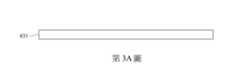
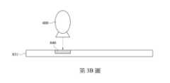
第3A圖至第3D圖分別為第2圖之步驟21之電路子板830的連續操作示意圖。具體地,步驟21更依據如下之數個細部步驟以製作每個電路子板830。首先,如第3A圖所示,提供一電路板基板831;接著,如第3B圖所示,形成第一圖形碼840於電路板基板831上,舉例來說,透過雷射打標裝置400將第一圖形碼840製作至電路板基板831上;接著,如第3C圖所示,將一金屬層832覆蓋於第一圖形碼840及電路板基板831上;接著,如第3C圖及第3D圖所示,將金屬層832製作為一遮蔽第一圖形碼840之線路圖案833。FIG. 3A to FIG. 3D are schematic diagrams of the continuous operation of the
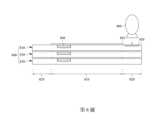
第4圖為第2圖之步驟22之操作示意圖。第5圖為第2圖之步驟23之操作示意圖。更具體地,如第4圖所示,步驟22更包含將多個電路子板830沿一壓合方向S彼此壓合為電路板產品800(第5圖),並且讓電路板產品800接受邊線研磨程序。此時,這些電路子板830之這些第一圖形碼840在壓合方向S為彼此重疊的。然而,本發明不限於此,其他實施例中亦可改讓這些電路子板830之這些第一圖形碼840在壓合方向S為彼此交錯的。FIG. 4 is a schematic diagram of the operation of
第5圖為第2圖之步驟23之操作示意圖。更進一步地,如第5圖所示,步驟23更包含之細部步驟為透過X光讀碼裝置300朝壓合方向S依序照射並讀取這些電路子板830的這些第一圖形碼840。如此,當終端裝置700啟動X光讀碼裝置300,並取得X光讀碼裝置300所依序讀取的這些第一圖形碼840時,終端裝置700將這些第一圖形碼840記錄至資料庫裝置200內、指示此條碼生成單元500生成第二圖形碼850、將第二圖形碼850記錄至資料庫裝置200內,並將此些第一圖形碼840對應至第二圖形碼850。FIG. 5 is a schematic diagram of the operation of
進一步地,終端裝置700將第二圖形碼850、對應此第二圖形碼850之電路板產品800之序號、此些電路子板830於電路板產品800上之層疊順序,以及每個電路子板830之生產履歷資料記錄至資料庫裝置200內。Furthermore, the
第6圖為第2圖之步驟24之操作示意圖。更進一步地,如第6圖所示,步驟24更包含透過雷射打標裝置400將第二圖形碼850製作至電路板產品800之外表面801。舉例來說,當電路板產品800沿著水平方向H分為電路區域810及其環繞電路區域810之非電路區域820時,雷射打標裝置400將第二圖形碼850製作至電路板產品800之非電路區域820,然而,本發明不限於此。FIG. 6 is a schematic diagram of the operation of
另外,在第二圖形碼850被生成,或者製作至電路板產品800之後,終端裝置700將第二圖形碼850對應此第二圖形碼850之電路板產品800之序號及生產履歷資料及此些電路子板830於電路板產品800上之層疊順序等相關軌跡訊息記錄至資料庫裝置200內。In addition, after the second
第7圖為透過光學讀碼裝置600讀取第二圖形碼850的操作示意圖。如第7圖所示,當任一檢驗人員透過光學讀碼裝置600朝壓合方向S對準且讀取電路板產品800之第二圖形碼850時,終端裝置700不僅從資料庫裝置200內取得對應第二圖形碼850之相關軌跡訊息,更能夠檢視對應此第二圖形碼850之所有電路子板830之層疊順序及其生產履歷資料。FIG. 7 is a schematic diagram of the operation of reading the second
須了解到,在上述所有實施例中,第一圖形碼840及第二圖形碼850分別為二維碼,且第一圖形碼840及第二圖形碼850分別為電路板基板831上之貫孔。然而,本發明不限於此,其他實施例中亦可讓第一圖形碼840及第二圖形碼850改為一維碼,或者,改為電路板基板831上之盲孔。It should be understood that in all the above embodiments, the first
如此,透過以上架構,本發明之電路板產品之電路子板之原料來源、入庫、出庫、生產廠區、品質檢驗及後續處置等之生產履歷資料都能被有效地記錄及追蹤,有助生產成本、生產週期和生產效率的控制,從而大大提高產品的競爭力。Thus, through the above structure, the production history data of the circuit board products of the present invention, such as the source of raw materials, warehousing, delivery, production plant, quality inspection and subsequent disposal, can be effectively recorded and tracked, which helps to control the production cost, production cycle and production efficiency, thereby greatly improving the competitiveness of the product.
最後,上述所揭露之各實施例中,並非用以限定本發明,任何熟習此技藝者,在不脫離本發明之精神和範圍內,當可作各種之更動與潤飾,皆可被保護於本發明中。因此本發明之保護範圍當視後附之申請專利範圍所界定者為準。Finally, the above disclosed embodiments are not intended to limit the present invention. Anyone skilled in the art can make various changes and modifications within the spirit and scope of the present invention, and all of them can be protected by the present invention. Therefore, the protection scope of the present invention shall be determined by the scope of the attached patent application.
10:製作系統 21~24:步驟 100:壓合裝置 200:資料庫裝置 300:X光讀碼裝置 400:雷射打標裝置 500:條碼生成單元 600:光學讀碼裝置 700:終端裝置 800:電路板產品 801:外表面 810:電路區域 820:非電路區域 830:電路子板 831:電路板基板 832:金屬層 833:線路圖案 840:第一圖形碼 850:第二圖形碼 H:水平方向 S:壓合方向10:
為讓本發明之上述和其他目的、特徵、優點與實施例能更明顯易懂,所附圖式之說明如下: 第1圖為本發明一實施例之有助源頭追溯之電路板之製作系統的方塊圖。 第2圖為本發明一實施例之有助源頭追溯之電路板之製作方法的流程圖。 第3A圖至第3D圖分別為第2圖之步驟21之電路子板的連續操作示意圖。 第4圖為第2圖之步驟22之操作示意圖。 第5圖為第2圖之步驟23之操作示意圖。 第6圖為第2圖之步驟24之操作示意圖。 第7圖為透過光學讀碼裝置讀取第二圖形碼的操作示意圖。In order to make the above and other purposes, features, advantages and embodiments of the present invention more clearly understandable, the attached drawings are described as follows: FIG. 1 is a block diagram of a circuit board manufacturing system that facilitates source tracing of an embodiment of the present invention. FIG. 2 is a flow chart of a circuit board manufacturing method that facilitates source tracing of an embodiment of the present invention. FIG. 3A to FIG. 3D are respectively schematic diagrams of the continuous operation of the circuit board of
國內寄存資訊(請依寄存機構、日期、號碼順序註記) 無 國外寄存資訊(請依寄存國家、機構、日期、號碼順序註記) 無Domestic storage information (please note in the order of storage institution, date, and number)NoneForeign storage information (please note in the order of storage country, institution, date, and number)None
21~24:步驟21~24: Steps
Claims (7)
Translated fromChinesePriority Applications (1)
| Application Number | Priority Date | Filing Date | Title |
|---|---|---|---|
| TW112149884ATWI870172B (en) | 2023-12-20 | 2023-12-20 | Method of manufacturing circuit boards with source traceability and system for manufacturing the same |
Applications Claiming Priority (1)
| Application Number | Priority Date | Filing Date | Title |
|---|---|---|---|
| TW112149884ATWI870172B (en) | 2023-12-20 | 2023-12-20 | Method of manufacturing circuit boards with source traceability and system for manufacturing the same |
Publications (2)
| Publication Number | Publication Date |
|---|---|
| TWI870172Btrue TWI870172B (en) | 2025-01-11 |
| TW202527330A TW202527330A (en) | 2025-07-01 |
Family
ID=95151762
Family Applications (1)
| Application Number | Title | Priority Date | Filing Date |
|---|---|---|---|
| TW112149884ATWI870172B (en) | 2023-12-20 | 2023-12-20 | Method of manufacturing circuit boards with source traceability and system for manufacturing the same |
Country Status (1)
| Country | Link |
|---|---|
| TW (1) | TWI870172B (en) |
Citations (5)
| Publication number | Priority date | Publication date | Assignee | Title |
|---|---|---|---|---|
| US20060086794A1 (en)* | 1999-06-07 | 2006-04-27 | Metrologic Instruments, Inc.. | X-radiation scanning system having an automatic object identification and attribute information acquisition and linking mechanism integrated therein |
| US20080166497A1 (en)* | 2004-04-22 | 2008-07-10 | Shih-Ping Hsu | Circuit board with identifiable information and method for fabricating the same |
| TW201146109A (en)* | 2010-06-15 | 2011-12-16 | Foxconn Advanced Tech Inc | Method for tracing quality of printed circuit board |
| TW201519705A (en)* | 2013-11-08 | 2015-05-16 | Prov Technology Corp | Bar code reading method of multilayer circuit board |
| CN110400152A (en)* | 2018-04-17 | 2019-11-01 | 鹏鼎控股(深圳)股份有限公司 | Quality traceability system for printed circuit board |
- 2023
- 2023-12-20TWTW112149884Apatent/TWI870172B/enactive
Patent Citations (5)
| Publication number | Priority date | Publication date | Assignee | Title |
|---|---|---|---|---|
| US20060086794A1 (en)* | 1999-06-07 | 2006-04-27 | Metrologic Instruments, Inc.. | X-radiation scanning system having an automatic object identification and attribute information acquisition and linking mechanism integrated therein |
| US20080166497A1 (en)* | 2004-04-22 | 2008-07-10 | Shih-Ping Hsu | Circuit board with identifiable information and method for fabricating the same |
| TW201146109A (en)* | 2010-06-15 | 2011-12-16 | Foxconn Advanced Tech Inc | Method for tracing quality of printed circuit board |
| TW201519705A (en)* | 2013-11-08 | 2015-05-16 | Prov Technology Corp | Bar code reading method of multilayer circuit board |
| CN110400152A (en)* | 2018-04-17 | 2019-11-01 | 鹏鼎控股(深圳)股份有限公司 | Quality traceability system for printed circuit board |
Also Published As
| Publication number | Publication date |
|---|---|
| TW202527330A (en) | 2025-07-01 |
Similar Documents
| Publication | Publication Date | Title |
|---|---|---|
| US10602651B2 (en) | System for tracing printed circuit boards through manufacturing stages | |
| KR101019762B1 (en) | Forming method and apparatus for forming two-dimensional code | |
| CN111372382A (en) | Primary and secondary board pressing alignment design process method of PCB | |
| CN105678362A (en) | Traceability method of power module | |
| Chang et al. | An implementation of health prediction in SMT solder joint via machine learning | |
| CN113573506B (en) | PCB production process and PCB circuit board | |
| TWI870172B (en) | Method of manufacturing circuit boards with source traceability and system for manufacturing the same | |
| JP2881418B1 (en) | Silicon substrate with identification data and method of manufacturing the same | |
| TWI391052B (en) | Method for tracing quality of printed circuit board | |
| JPWO2010070964A1 (en) | Circuit module and management method thereof | |
| TWI381780B (en) | Manufacturing method for identifiable pcb | |
| CN110399937B (en) | Information detection method for printed circuit board | |
| JP3046697B2 (en) | Exposure equipment | |
| CN115696773A (en) | Laser welding-proof layer removing process method for substrate | |
| CN117651373B (en) | A circuit board manufacturing method and manufacturing system that facilitates source tracing | |
| JP4483874B2 (en) | Multi-chip substrate | |
| US20090101391A1 (en) | Circuit board having barcode and fabrication method thereof | |
| TW201608681A (en) | Substrate structure and method of manufacture | |
| CN111278230A (en) | Method for screening negative films of printed circuit boards | |
| CN116133290A (en) | Processing method of multilayer PCB with manufacturing flow tracing two-dimensional code | |
| TWI402010B (en) | Manufacturing procedure and manufacturing system for integrated circuit module | |
| JP7678433B2 (en) | Laser beam removal process for solder resist on substrate | |
| TW201733888A (en) | Printed circuit board classification method capable of effectively enhancing classification efficiency to obtain shrinkage classification or batch by way of reading | |
| KR20210103597A (en) | Method of marking the printed circuit board pannel | |
| TWI413872B (en) | Marking system of printed circuit board and method for using the same |