TWI866482B - Light-emitting device, display apparatus including the same and method for manufacturing the same - Google Patents
Light-emitting device, display apparatus including the same and method for manufacturing the sameDownload PDFInfo
- Publication number
- TWI866482B TWI866482BTW112135871ATW112135871ATWI866482BTW I866482 BTWI866482 BTW I866482BTW 112135871 ATW112135871 ATW 112135871ATW 112135871 ATW112135871 ATW 112135871ATW I866482 BTWI866482 BTW I866482B
- Authority
- TW
- Taiwan
- Prior art keywords
- semiconductor layer
- emitting device
- layer
- light
- disposed
- Prior art date
Links
Images


Classifications
- H—ELECTRICITY
- H10—SEMICONDUCTOR DEVICES; ELECTRIC SOLID-STATE DEVICES NOT OTHERWISE PROVIDED FOR
- H10H—INORGANIC LIGHT-EMITTING SEMICONDUCTOR DEVICES HAVING POTENTIAL BARRIERS
- H10H20/00—Individual inorganic light-emitting semiconductor devices having potential barriers, e.g. light-emitting diodes [LED]
- H10H20/80—Constructional details
- H10H20/81—Bodies
- H10H20/819—Bodies characterised by their shape, e.g. curved or truncated substrates
- H—ELECTRICITY
- H01—ELECTRIC ELEMENTS
- H01L—SEMICONDUCTOR DEVICES NOT COVERED BY CLASS H10
- H01L24/00—Arrangements for connecting or disconnecting semiconductor or solid-state bodies; Methods or apparatus related thereto
- H01L24/93—Batch processes
- H01L24/95—Batch processes at chip-level, i.e. with connecting carried out on a plurality of singulated devices, i.e. on diced chips
- H01L24/97—Batch processes at chip-level, i.e. with connecting carried out on a plurality of singulated devices, i.e. on diced chips the devices being connected to a common substrate, e.g. interposer, said common substrate being separable into individual assemblies after connecting
- H—ELECTRICITY
- H01—ELECTRIC ELEMENTS
- H01L—SEMICONDUCTOR DEVICES NOT COVERED BY CLASS H10
- H01L25/00—Assemblies consisting of a plurality of semiconductor or other solid state devices
- H01L25/03—Assemblies consisting of a plurality of semiconductor or other solid state devices all the devices being of a type provided for in a single subclass of subclasses H10B, H10D, H10F, H10H, H10K or H10N, e.g. assemblies of rectifier diodes
- H01L25/04—Assemblies consisting of a plurality of semiconductor or other solid state devices all the devices being of a type provided for in a single subclass of subclasses H10B, H10D, H10F, H10H, H10K or H10N, e.g. assemblies of rectifier diodes the devices not having separate containers
- H01L25/075—Assemblies consisting of a plurality of semiconductor or other solid state devices all the devices being of a type provided for in a single subclass of subclasses H10B, H10D, H10F, H10H, H10K or H10N, e.g. assemblies of rectifier diodes the devices not having separate containers the devices being of a type provided for in group H10H20/00
- H01L25/0753—Assemblies consisting of a plurality of semiconductor or other solid state devices all the devices being of a type provided for in a single subclass of subclasses H10B, H10D, H10F, H10H, H10K or H10N, e.g. assemblies of rectifier diodes the devices not having separate containers the devices being of a type provided for in group H10H20/00 the devices being arranged next to each other
- H—ELECTRICITY
- H10—SEMICONDUCTOR DEVICES; ELECTRIC SOLID-STATE DEVICES NOT OTHERWISE PROVIDED FOR
- H10D—INORGANIC ELECTRIC SEMICONDUCTOR DEVICES
- H10D86/00—Integrated devices formed in or on insulating or conducting substrates, e.g. formed in silicon-on-insulator [SOI] substrates or on stainless steel or glass substrates
- H10D86/01—Manufacture or treatment
- H10D86/021—Manufacture or treatment of multiple TFTs
- H—ELECTRICITY
- H10—SEMICONDUCTOR DEVICES; ELECTRIC SOLID-STATE DEVICES NOT OTHERWISE PROVIDED FOR
- H10D—INORGANIC ELECTRIC SEMICONDUCTOR DEVICES
- H10D86/00—Integrated devices formed in or on insulating or conducting substrates, e.g. formed in silicon-on-insulator [SOI] substrates or on stainless steel or glass substrates
- H10D86/40—Integrated devices formed in or on insulating or conducting substrates, e.g. formed in silicon-on-insulator [SOI] substrates or on stainless steel or glass substrates characterised by multiple TFTs
- H10D86/441—Interconnections, e.g. scanning lines
- H—ELECTRICITY
- H10—SEMICONDUCTOR DEVICES; ELECTRIC SOLID-STATE DEVICES NOT OTHERWISE PROVIDED FOR
- H10H—INORGANIC LIGHT-EMITTING SEMICONDUCTOR DEVICES HAVING POTENTIAL BARRIERS
- H10H20/00—Individual inorganic light-emitting semiconductor devices having potential barriers, e.g. light-emitting diodes [LED]
- H10H20/01—Manufacture or treatment
- H10H20/011—Manufacture or treatment of bodies, e.g. forming semiconductor layers
- H10H20/013—Manufacture or treatment of bodies, e.g. forming semiconductor layers having light-emitting regions comprising only Group III-V materials
- H10H20/0133—Manufacture or treatment of bodies, e.g. forming semiconductor layers having light-emitting regions comprising only Group III-V materials with a substrate not being Group III-V materials
- H10H20/01335—Manufacture or treatment of bodies, e.g. forming semiconductor layers having light-emitting regions comprising only Group III-V materials with a substrate not being Group III-V materials the light-emitting regions comprising nitride materials
- H—ELECTRICITY
- H10—SEMICONDUCTOR DEVICES; ELECTRIC SOLID-STATE DEVICES NOT OTHERWISE PROVIDED FOR
- H10H—INORGANIC LIGHT-EMITTING SEMICONDUCTOR DEVICES HAVING POTENTIAL BARRIERS
- H10H20/00—Individual inorganic light-emitting semiconductor devices having potential barriers, e.g. light-emitting diodes [LED]
- H10H20/01—Manufacture or treatment
- H10H20/011—Manufacture or treatment of bodies, e.g. forming semiconductor layers
- H10H20/013—Manufacture or treatment of bodies, e.g. forming semiconductor layers having light-emitting regions comprising only Group III-V materials
- H10H20/0137—Manufacture or treatment of bodies, e.g. forming semiconductor layers having light-emitting regions comprising only Group III-V materials the light-emitting regions comprising nitride materials
- H—ELECTRICITY
- H10—SEMICONDUCTOR DEVICES; ELECTRIC SOLID-STATE DEVICES NOT OTHERWISE PROVIDED FOR
- H10H—INORGANIC LIGHT-EMITTING SEMICONDUCTOR DEVICES HAVING POTENTIAL BARRIERS
- H10H20/00—Individual inorganic light-emitting semiconductor devices having potential barriers, e.g. light-emitting diodes [LED]
- H10H20/01—Manufacture or treatment
- H10H20/011—Manufacture or treatment of bodies, e.g. forming semiconductor layers
- H10H20/018—Bonding of wafers
- H—ELECTRICITY
- H10—SEMICONDUCTOR DEVICES; ELECTRIC SOLID-STATE DEVICES NOT OTHERWISE PROVIDED FOR
- H10H—INORGANIC LIGHT-EMITTING SEMICONDUCTOR DEVICES HAVING POTENTIAL BARRIERS
- H10H20/00—Individual inorganic light-emitting semiconductor devices having potential barriers, e.g. light-emitting diodes [LED]
- H10H20/80—Constructional details
- H10H20/81—Bodies
- H10H20/811—Bodies having quantum effect structures or superlattices, e.g. tunnel junctions
- H—ELECTRICITY
- H10—SEMICONDUCTOR DEVICES; ELECTRIC SOLID-STATE DEVICES NOT OTHERWISE PROVIDED FOR
- H10H—INORGANIC LIGHT-EMITTING SEMICONDUCTOR DEVICES HAVING POTENTIAL BARRIERS
- H10H20/00—Individual inorganic light-emitting semiconductor devices having potential barriers, e.g. light-emitting diodes [LED]
- H10H20/80—Constructional details
- H10H20/81—Bodies
- H10H20/819—Bodies characterised by their shape, e.g. curved or truncated substrates
- H10H20/821—Bodies characterised by their shape, e.g. curved or truncated substrates of the light-emitting regions, e.g. non-planar junctions
- H—ELECTRICITY
- H10—SEMICONDUCTOR DEVICES; ELECTRIC SOLID-STATE DEVICES NOT OTHERWISE PROVIDED FOR
- H10H—INORGANIC LIGHT-EMITTING SEMICONDUCTOR DEVICES HAVING POTENTIAL BARRIERS
- H10H20/00—Individual inorganic light-emitting semiconductor devices having potential barriers, e.g. light-emitting diodes [LED]
- H10H20/80—Constructional details
- H10H20/81—Bodies
- H10H20/822—Materials of the light-emitting regions
- H10H20/824—Materials of the light-emitting regions comprising only Group III-V materials, e.g. GaP
- H10H20/825—Materials of the light-emitting regions comprising only Group III-V materials, e.g. GaP containing nitrogen, e.g. GaN
- H—ELECTRICITY
- H10—SEMICONDUCTOR DEVICES; ELECTRIC SOLID-STATE DEVICES NOT OTHERWISE PROVIDED FOR
- H10H—INORGANIC LIGHT-EMITTING SEMICONDUCTOR DEVICES HAVING POTENTIAL BARRIERS
- H10H20/00—Individual inorganic light-emitting semiconductor devices having potential barriers, e.g. light-emitting diodes [LED]
- H10H20/80—Constructional details
- H10H20/84—Coatings, e.g. passivation layers or antireflective coatings
- H—ELECTRICITY
- H10—SEMICONDUCTOR DEVICES; ELECTRIC SOLID-STATE DEVICES NOT OTHERWISE PROVIDED FOR
- H10H—INORGANIC LIGHT-EMITTING SEMICONDUCTOR DEVICES HAVING POTENTIAL BARRIERS
- H10H20/00—Individual inorganic light-emitting semiconductor devices having potential barriers, e.g. light-emitting diodes [LED]
- H10H20/80—Constructional details
- H10H20/85—Packages
- H10H20/8506—Containers
- H—ELECTRICITY
- H10—SEMICONDUCTOR DEVICES; ELECTRIC SOLID-STATE DEVICES NOT OTHERWISE PROVIDED FOR
- H10H—INORGANIC LIGHT-EMITTING SEMICONDUCTOR DEVICES HAVING POTENTIAL BARRIERS
- H10H20/00—Individual inorganic light-emitting semiconductor devices having potential barriers, e.g. light-emitting diodes [LED]
- H10H20/80—Constructional details
- H10H20/85—Packages
- H10H20/855—Optical field-shaping means, e.g. lenses
- H—ELECTRICITY
- H10—SEMICONDUCTOR DEVICES; ELECTRIC SOLID-STATE DEVICES NOT OTHERWISE PROVIDED FOR
- H10H—INORGANIC LIGHT-EMITTING SEMICONDUCTOR DEVICES HAVING POTENTIAL BARRIERS
- H10H20/00—Individual inorganic light-emitting semiconductor devices having potential barriers, e.g. light-emitting diodes [LED]
- H10H20/80—Constructional details
- H10H20/85—Packages
- H10H20/857—Interconnections, e.g. lead-frames, bond wires or solder balls
- H—ELECTRICITY
- H01—ELECTRIC ELEMENTS
- H01L—SEMICONDUCTOR DEVICES NOT COVERED BY CLASS H10
- H01L25/00—Assemblies consisting of a plurality of semiconductor or other solid state devices
- H01L25/16—Assemblies consisting of a plurality of semiconductor or other solid state devices the devices being of types provided for in two or more different subclasses of H10B, H10D, H10F, H10H, H10K or H10N, e.g. forming hybrid circuits
- H01L25/167—Assemblies consisting of a plurality of semiconductor or other solid state devices the devices being of types provided for in two or more different subclasses of H10B, H10D, H10F, H10H, H10K or H10N, e.g. forming hybrid circuits comprising optoelectronic devices, e.g. LED, photodiodes
- H—ELECTRICITY
- H01—ELECTRIC ELEMENTS
- H01L—SEMICONDUCTOR DEVICES NOT COVERED BY CLASS H10
- H01L2924/00—Indexing scheme for arrangements or methods for connecting or disconnecting semiconductor or solid-state bodies as covered by H01L24/00
- H01L2924/10—Details of semiconductor or other solid state devices to be connected
- H01L2924/11—Device type
- H01L2924/12—Passive devices, e.g. 2 terminal devices
- H01L2924/1204—Optical Diode
- H01L2924/12041—LED
- H—ELECTRICITY
- H10—SEMICONDUCTOR DEVICES; ELECTRIC SOLID-STATE DEVICES NOT OTHERWISE PROVIDED FOR
- H10H—INORGANIC LIGHT-EMITTING SEMICONDUCTOR DEVICES HAVING POTENTIAL BARRIERS
- H10H20/00—Individual inorganic light-emitting semiconductor devices having potential barriers, e.g. light-emitting diodes [LED]
- H10H20/01—Manufacture or treatment
- H10H20/034—Manufacture or treatment of coatings
- H—ELECTRICITY
- H10—SEMICONDUCTOR DEVICES; ELECTRIC SOLID-STATE DEVICES NOT OTHERWISE PROVIDED FOR
- H10H—INORGANIC LIGHT-EMITTING SEMICONDUCTOR DEVICES HAVING POTENTIAL BARRIERS
- H10H20/00—Individual inorganic light-emitting semiconductor devices having potential barriers, e.g. light-emitting diodes [LED]
- H10H20/01—Manufacture or treatment
- H10H20/036—Manufacture or treatment of packages
- H10H20/0364—Manufacture or treatment of packages of interconnections
- H—ELECTRICITY
- H10—SEMICONDUCTOR DEVICES; ELECTRIC SOLID-STATE DEVICES NOT OTHERWISE PROVIDED FOR
- H10H—INORGANIC LIGHT-EMITTING SEMICONDUCTOR DEVICES HAVING POTENTIAL BARRIERS
- H10H20/00—Individual inorganic light-emitting semiconductor devices having potential barriers, e.g. light-emitting diodes [LED]
- H10H20/80—Constructional details
- H10H20/882—Scattering means
Landscapes
- Engineering & Computer Science (AREA)
- Microelectronics & Electronic Packaging (AREA)
- Power Engineering (AREA)
- Computer Hardware Design (AREA)
- Physics & Mathematics (AREA)
- Condensed Matter Physics & Semiconductors (AREA)
- General Physics & Mathematics (AREA)
- Led Devices (AREA)
- Led Device Packages (AREA)
- Manufacturing & Machinery (AREA)
Abstract
Description
Translated fromChinese本發明涉及一種發光裝置,特別是一種包含能夠防止發光裝置毀損的結構的發光裝置、一種包含所述發光裝置的顯示設備,以及一種所述顯示設備的製造方法。The present invention relates to a light-emitting device, in particular to a light-emitting device comprising a structure capable of preventing the light-emitting device from being damaged, a display device comprising the light-emitting device, and a method for manufacturing the display device.
顯示設備已被應用於例如電視機(TV)、行動電話、筆記型電腦以及平板等的各種電子裝置。在這些顯示設備中,發光顯示設備具有內建的發光元件或光源,且藉由使用從內建的發光元件或光源產生的光來顯示資訊。包含自發光元件的顯示設備可被實施成比具有內建的光源的顯示設備還薄,且可被實施為可被摺疊、彎曲或捲繞的可撓式顯示設備。Display devices have been applied to various electronic devices such as televisions (TVs), mobile phones, laptops, and tablets. Among these display devices, a light-emitting display device has a built-in light-emitting element or light source, and displays information by using light generated from the built-in light-emitting element or light source. A display device including a self-luminous element can be implemented to be thinner than a display device having a built-in light source, and can be implemented as a flexible display device that can be folded, bent, or rolled.
舉例來說,具有自發光元件的顯示設備可包含:包含由有機材料製成的發光層的有機發光顯示設備(OLED),或包含由無機材料製成的發光層的微型LED顯示設備(微型發光二極體顯示設備)。在這方面,有機發光顯示設備不需要獨立的光源。然而,因為易受濕氣以及氧氣影響的有機材料的材料特性,所以透過外部環境於有機發光顯示設備中可能容易發生有缺陷的像素。For example, a display device having a self-luminous element may include an organic light-emitting display device (OLED) including a light-emitting layer made of an organic material, or a micro-LED display device (micro-LED display device) including a light-emitting layer made of an inorganic material. In this regard, an organic light-emitting display device does not require an independent light source. However, due to the material properties of organic materials that are susceptible to moisture and oxygen, defective pixels may easily occur in an organic light-emitting display device through the external environment.
相反地,微型LED顯示設備包含由能抵抗濕氣以及氧氣的無機材料製成的發光層,且因此可不受外部環境影響,且因此可相較於有機發光顯示設備提供良好的可靠性且具有長的壽命。In contrast, the micro LED display device includes a light-emitting layer made of an inorganic material that is resistant to moisture and oxygen, and thus may not be affected by the external environment, and thus may provide good reliability and have a long life compared to an organic light-emitting display device.
再者,微型LED顯示設備可抵抗外部環境,且因此可不需要例如密封材料等的保護性結構,且各種類型的材料可被用作為設備的基板的材料。因此,微型LED顯示設備可被製成比有機發光顯示設備更薄,且可更有利於被實施為可撓式顯示設備。Furthermore, the micro LED display device can resist the external environment and thus may not require a protective structure such as a sealing material, and various types of materials may be used as a material for a substrate of the device. Therefore, the micro LED display device can be made thinner than an organic light emitting display device and may be more advantageously implemented as a flexible display device.
再者,多個微型LED能彼此連接,以實施大面積的顯示設備。因此,微型LED顯示設備作為下一代的顯示設備而備受矚目。Furthermore, a plurality of micro LEDs can be connected to each other to implement a large-area display device. Therefore, micro LED display devices are attracting much attention as next-generation display devices.
因此,正在進行研究,以在增加微型LED顯示設備的發光效率的同時改善微型LED顯示設備的特性。Therefore, research is being conducted to improve the characteristics of the micro LED display device while increasing the light emission efficiency of the micro LED display device.
因此,本發明涉及一種實質上消除因上述的限制以及缺點所導致的一個或多個問題的發光裝置、包含其的顯示設備及其製造方法。Therefore, the present invention relates to a light emitting device, a display device including the same, and a manufacturing method thereof, which substantially eliminates one or more problems caused by the above-mentioned limitations and disadvantages.
更具體來說,本發明在於提供一種發光裝置,其能夠防止因發生於雷射剝離製程中的裂縫缺陷等而導致的發光裝置晶片的特性的劣化。More specifically, the present invention provides a light emitting device that can prevent the degradation of the characteristics of a light emitting device chip due to crack defects or the like occurring during a laser lift-off process.
本發明也在於減少氮化物半導體結構和生長基板之間的接觸區域,以提供相對厚的鈍化圖案,進而保護氮化物半導體結構的側表面,且因此補償外部量子效率的下降。The present invention also aims to reduce the contact area between the nitride semiconductor structure and the growth substrate to provide a relatively thick passivation pattern, thereby protecting the side surface of the nitride semiconductor structure and thus compensating for the decrease in external quantum efficiency.
再者,本發明在於減少氮化物半導體結構和生長基板之間的接觸區域,以減少相鄰的多個發光裝置晶片之間的空間餘裕,進而增加發光裝置晶片的密度,且因此改善產量且使製程最佳化。Furthermore, the present invention is to reduce the contact area between the nitride semiconductor structure and the growth substrate to reduce the space margin between adjacent light emitting device chips, thereby increasing the density of the light emitting device chips, and thus improving the yield and optimizing the process.
再者,本發明在於提供一種顯示設備及其製造方法,其中將多個發光裝置晶片結合至封裝基板時,將氮化物半導體結構的底突出部插入封裝基板的固持區域中的同時多個發光裝置晶片中的每一者會固定至封裝基板,因而防止這些發光裝置晶片的錯位。Furthermore, the present invention provides a display device and a manufacturing method thereof, wherein when a plurality of light-emitting device chips are bonded to a packaging substrate, each of the plurality of light-emitting device chips is fixed to the packaging substrate while the bottom protrusion of the nitride semiconductor structure is inserted into the holding area of the packaging substrate, thereby preventing the light-emitting device chips from being misaligned.
本發明不以上述提及的特徵為限。可基於以下描述理解根據本發明的未提及的其他特徵以及優點,且可更清楚地理解基於根據本發明的態樣。再者,將容易理解的是,可使用請求項中所示的手段或其組合來實現根據本發明的目的以及優點。The present invention is not limited to the above-mentioned features. Other features and advantages not mentioned according to the present invention can be understood based on the following description, and the aspects according to the present invention can be more clearly understood. Furthermore, it will be easily understood that the objects and advantages according to the present invention can be achieved by using the means shown in the claims or their combination.
在本發明的一態樣中,發光裝置包含:包含依序地設置的第一半導體層、主動層以及第二半導體層的氮化物半導體結構;以及設置於氮化物半導體結構的外表面上的鈍化圖案,其中第一半導體層包含突出部,突出部沿著遠離主動層的方向突出。In one aspect of the present invention, the light emitting device includes: a nitride semiconductor structure including a first semiconductor layer, an active layer, and a second semiconductor layer arranged in sequence; and a passivation pattern arranged on the outer surface of the nitride semiconductor structure, wherein the first semiconductor layer includes a protrusion, and the protrusion protrudes in a direction away from the active layer.
在本發明的另一態樣中,顯示設備包含封裝基板以及發光裝置,其中封裝基板設置有多個電路元件,封裝基板包含固持區域;其中發光裝置包含:包含依序地設置的第一半導體層、主動層以及第二半導體層的氮化物半導體結構;以及設置於氮化物半導體結構的外表面上的鈍化圖案,其中第一半導體層包含突出部,突出部沿著遠離主動層的方向突出,其中突出部設置於固持區域中。In another aspect of the present invention, a display device includes a packaging substrate and a light-emitting device, wherein the packaging substrate is provided with a plurality of circuit elements, and the packaging substrate includes a holding region; wherein the light-emitting device includes: a nitride semiconductor structure including a first semiconductor layer, an active layer, and a second semiconductor layer arranged in sequence; and a passivation pattern arranged on an outer surface of the nitride semiconductor structure, wherein the first semiconductor layer includes a protrusion, the protrusion protruding in a direction away from the active layer, wherein the protrusion is arranged in the holding region.
在本發明的又另一態樣中,顯示設備包含設置有多個電路元件的封裝基板;以及發光裝置,其中發光裝置包含:包含依序地設置的第一半導體層、主動層以及第二半導體層的氮化物半導體結構;以及設置於氮化物半導體結構的外表面上的鈍化圖案,其中發光裝置以及封裝基板經由導電黏合材料彼此結合。In yet another aspect of the present invention, a display device includes a package substrate having a plurality of circuit elements disposed thereon; and a light-emitting device, wherein the light-emitting device includes: a nitride semiconductor structure including a first semiconductor layer, an active layer, and a second semiconductor layer disposed in sequence; and a passivation pattern disposed on an outer surface of the nitride semiconductor structure, wherein the light-emitting device and the package substrate are bonded to each other via a conductive adhesive material.
在本發明的又再另一態樣中,顯示設備的製造方法包含:提供發光裝置,其中發光裝置包含氮化物半導體結構,以及設置於氮化物半導體結構的外表面上的鈍化圖案,其中氮化物半導體結構包含依序地設置的第一半導體層、主動層以及第二半導體層,其中第一半導體層包含下部部分以及相較於下部部分具有更大的寬度的上部部分;提供封裝基板,所述封裝基板具有界定於其中且與發光裝置對齊的固持區域,其中用於驅動發光裝置的多個電路元件設置於封裝基板中;將第一半導體層的下部部分置於固持區域中;以及將封裝基板以及發光裝置彼此結合。In yet another aspect of the present invention, a method for manufacturing a display device includes: providing a light-emitting device, wherein the light-emitting device includes a nitride semiconductor structure, and a passivation pattern disposed on an outer surface of the nitride semiconductor structure, wherein the nitride semiconductor structure includes a first semiconductor layer, an active layer, and a second semiconductor layer disposed in sequence, wherein the first semiconductor layer includes a lower portion and an upper portion having a larger width than the lower portion; providing a packaging substrate, wherein the packaging substrate has a holding area defined therein and aligned with the light-emitting device, wherein a plurality of circuit elements for driving the light-emitting device are disposed in the packaging substrate; placing the lower portion of the first semiconductor layer in the holding area; and bonding the packaging substrate and the light-emitting device to each other.
在本發明的進一步態樣中,發光裝置包含依序地設置的第一半導體層、主動層以及第二半導體層;以及設置於第一半導體層、主動層以及第二半導體層的外表面上的鈍化圖案,其中第一半導體層包含:具有第一寬度的第一部分;以及相較於第一部分被設置成更接近主動層且具有大於第一寬度的第二寬度的第二部分。In a further aspect of the present invention, the light-emitting device includes a first semiconductor layer, an active layer, and a second semiconductor layer arranged in sequence; and a passivation pattern arranged on the outer surfaces of the first semiconductor layer, the active layer, and the second semiconductor layer, wherein the first semiconductor layer includes: a first portion having a first width; and a second portion which is arranged closer to the active layer than the first portion and has a second width greater than the first width.
根據本發明的各種態樣,遮罩圖案可設置於生長基板和氮化物半導體結構之間,而可減少生長基板和氮化物半導體結構之間的接觸區域。因此,會有在雷射剝離製程中減少發生於生長基板和氮化物半導體結構之間的裂縫缺陷的功效。According to various aspects of the present invention, a mask pattern can be disposed between a growth substrate and a nitride semiconductor structure, thereby reducing the contact area between the growth substrate and the nitride semiconductor structure. Therefore, it has the effect of reducing crack defects occurring between the growth substrate and the nitride semiconductor structure during a laser lift-off process.
再者,因為減少了在生長基板和氮化物半導體結構之間的接觸區域,所以會減少在雷射剝離製程期間雷射接觸的氮化物半導體結構的接觸區域。因此,可減少相鄰的多個發光裝置晶片之間的空間餘裕,進而增加發光裝置晶片的密度且改善產量。Furthermore, since the contact area between the growth substrate and the nitride semiconductor structure is reduced, the contact area of the nitride semiconductor structure that is contacted by the laser during the laser stripping process is reduced. Therefore, the space margin between adjacent light emitting device chips can be reduced, thereby increasing the density of the light emitting device chips and improving the yield.
再者,因為保護氮化物半導體結構的外表面的鈍化圖案遠離於生長基板,所以可減少雷射剝離製程中來自鈍化圖案的異物缺陷。Furthermore, because the passivation pattern protecting the outer surface of the nitride semiconductor structure is away from the growth substrate, foreign body defects from the passivation pattern during the laser lift-off process can be reduced.
再者,因為鈍化圖案遠離於生長基板,所以可確保鈍化圖案的足夠的厚度。因此,鈍化圖案的厚度在乾蝕刻製程中可足以防止可能會發生於氮化物半導體結構的側表面上的損毀,進而補償外部量子效率(EQE)的下降。Furthermore, since the passivation pattern is far from the growth substrate, a sufficient thickness of the passivation pattern can be ensured. Therefore, the thickness of the passivation pattern can be sufficient to prevent damage that may occur on the side surface of the nitride semiconductor structure during the dry etching process, thereby compensating for the reduction of external quantum efficiency (EQE).
此外,光散射圖案設置於氮化物半導體結構的第一半導體層的下部部分的側表面上,以引發光散射。因此,會有改善光提取效率的功效,且因此改善發光裝置晶片的效能。因此,需要相對小的電流以驅動發光裝置晶片,進而節省功耗。In addition, a light scattering pattern is provided on the side surface of the lower portion of the first semiconductor layer of the nitride semiconductor structure to induce light scattering. Therefore, there is an effect of improving light extraction efficiency, and thus improving the performance of the light emitting device chip. Therefore, a relatively small current is required to drive the light emitting device chip, thereby saving power consumption.
此外,氮化物半導體結構的第一半導體的下部部分具有突出形狀。因此,在將發光裝置結合至封裝基板的期間,發光裝置可固定地插入開放區域(固持區域)中。因此,多個發光裝置晶片可容易分別與封裝基板上的多個目標位置對齊,且因此能防止發光裝置的錯位。因此,可減少將這些發光裝置晶片與封裝基板上的多個目標位置對齊所需的時間,進而簡化顯示設備的製造製程。In addition, the lower portion of the first semiconductor of the nitride semiconductor structure has a protruding shape. Therefore, during the bonding of the light-emitting device to the packaging substrate, the light-emitting device can be fixedly inserted into the open area (holding area). Therefore, a plurality of light-emitting device chips can be easily aligned with a plurality of target positions on the packaging substrate, respectively, and thus misalignment of the light-emitting devices can be prevented. Therefore, the time required to align these light-emitting device chips with a plurality of target positions on the packaging substrate can be reduced, thereby simplifying the manufacturing process of the display device.
本發明的功效並不以上述提及的功效為限,且本領域中具有通常知識者將從以下描述清楚地理解未提及的其他功效。The effects of the present invention are not limited to the effects mentioned above, and those having ordinary knowledge in the art will clearly understand other effects not mentioned from the following description.
本發明之優點以及特徵及達成此優點與特徵的方法將詳細參照下述的態樣以及所附圖式而變得清晰。然而,本發明並不以以下揭露的態樣為限,且可以各種形式實施。因此,闡述這些態樣僅使本發明完整,且對本發明所屬技術領域中具有通常知識者完整地傳達本發明的範疇。The advantages and features of the present invention and the methods for achieving the advantages and features will become clear with reference to the following embodiments and the accompanying drawings. However, the present invention is not limited to the embodiments disclosed below and can be implemented in various forms. Therefore, these embodiments are described only to make the present invention complete and fully convey the scope of the present invention to those having ordinary knowledge in the technical field to which the present invention belongs.
圖式中所揭露的用於描述本發明的態樣之外形、尺寸、比例、角度、數量等等為示例性的,且本發明並不以此為限。於此,相同的標號代表相同的元件。再者,為了描述的簡潔,將省略周知的步驟以及元件的描述以及細節。再者,在本發明的以下詳細描述中,將闡述數個具體細節,以提供本發明的透徹理解。然而,將理解的是,可在沒有這些具體的細節的情況下實踐本發明。在其他情況下,周知的方法、步驟、元件與電路並未被詳細說明以免非必要地模糊本發明的態樣。The shapes, sizes, ratios, angles, quantities, etc. disclosed in the drawings for describing the aspects of the present invention are exemplary, and the present invention is not limited thereto. Herein, the same reference numerals represent the same elements. Furthermore, for the sake of brevity of description, the description and details of well-known steps and elements will be omitted. Furthermore, in the following detailed description of the present invention, several specific details will be elaborated to provide a thorough understanding of the present invention. However, it will be understood that the present invention can be practiced without these specific details. In other cases, well-known methods, steps, elements and circuits are not described in detail to avoid unnecessarily obscuring the aspects of the present invention.
在本文中使用到的特定術語只是為了說明特定態樣之目的,而非用以限制本發明。除非內文另有清楚指出,否則在本文中單個元件所使用的「一」和「一個」同時也包含多個元件。並且應更進一步了解在本說明書中所使用的「包含」、「包括」之用語指出所述特徵、整體、操作、元件,及/或構件的存在,但是並不排除其既有的或額外的一或多個其他特徵、整體、操作、元件、構件,及/或部分。如本文所用,用語「及/或」包括一個或多個關聯所列項目的任意或全部組合。像是在一列表的元件之後的「其中至少一者」的表達可修飾整個列表的元件而不是修飾所列出的個別元件。在解釋數值時,即使該處沒有明顯說明也可能發生誤差或是公差。The specific terms used in this article are only for the purpose of describing specific aspects and are not intended to limit the present invention. Unless otherwise clearly indicated in the text, the "one" and "an" used in this article for a single element also include multiple elements. It should be further understood that the terms "including" and "comprising" used in this specification indicate the existence of the characteristics, wholes, operations, elements, and/or components, but do not exclude one or more existing or additional other characteristics, wholes, operations, elements, components, and/or parts. As used herein, the term "and/or" includes any or all combinations of one or more associated listed items. Expressions such as "at least one of which" after a list of elements can modify the entire list of elements rather than modifying the individual elements listed. When interpreting numerical values, errors or tolerances may occur even if there is no obvious explanation there.
此外,應了解當第一元件或層被指出現在第二元件或層「之上」時,第一元件可被直接設置在第二元件上,或可間接地被放置在第二元件或層上且有第三元件或層放置在第一及第二元件或層之間。應理解當元件或層被指「連接於」或「耦合至」另一元件或層時,其可以是直接在、連接於或是耦合至另一元件或層,或是一個或以上介入元件或層可能會出現。此外,應理解當元件或層被指在兩個元件或層「之間」時,其可能是兩元件或層之間唯一的元件或層,或是有一個或以上介入元件可能會出現。Furthermore, it should be understood that when a first element or layer is referred to as being "on" a second element or layer, the first element may be directly disposed on the second element, or may be indirectly disposed on the second element or layer with a third element or layer disposed between the first and second elements or layers. It should be understood that when an element or layer is referred to as being "connected to" or "coupled to" another element or layer, it may be directly on, connected to, or coupled to the other element or layer, or one or more intervening elements or layers may be present. Furthermore, it should be understood that when an element or layer is referred to as being "between" two elements or layers, it may be the only element or layer between the two elements or layers, or one or more intervening elements may be present.
再者,如在本文中使用,當層、膜、區域、板或是其他類似物被設置在另一層、膜、區域、板或是其他類似物「上」或是「之上」時,前者可直接接觸後者,或同樣有另一層、膜、區域、板或是其他類似物可能在前者與後者之間。如在本文中使用,當層、膜、區域、板或是其他類似物被直接設置在另一層、膜、區域、板或是其他類似「上」或是「之上」時,前者可直接接觸於後者並且沒有又另一層、膜、區域、板或是其他類似物設置在前者與後者之間。更進一步,當層、膜、區域、板或是其他類似可被設置在另一層、膜、區域、板或是其他類似「下」或「之下」時,前者可以直接接觸於後者或另一層、膜、區域、板或是其他類似物可以被設置在前者與後者之間。如本文所用,當層、膜、區域、板或是其他類似物可被直接設置在另一層、膜、區域、板或是其他類似「下」或「之下」時,前者可直接接觸於後者並且又另一層、膜、區域、板或是其他類似物並不設置在前者與後者之間。Furthermore, as used herein, when a layer, film, region, plate or other similar object is disposed "on" or "over" another layer, film, region, plate or other similar object, the former may directly contact the latter, or there may be another layer, film, region, plate or other similar object between the former and the latter. As used herein, when a layer, film, region, plate or other similar object is directly disposed "on" or "over" another layer, film, region, plate or other similar object, the former may directly contact the latter and there may not be another layer, film, region, plate or other similar object disposed between the former and the latter. Furthermore, when a layer, film, region, plate or the like is disposed "under" or "beneath" another layer, film, region, plate or the like, the former may be in direct contact with the latter or another layer, film, region, plate or the like may be disposed between the former and the latter. As used herein, when a layer, film, region, plate or the like is disposed directly "under" or "beneath" another layer, film, region, plate or the like, the former may be in direct contact with the latter and another layer, film, region, plate or the like may not be disposed between the former and the latter.
在描述時間上的關係時,舉例來說,時間上的前例關係,像是「之後」、「隨後」、「之前」等,除非「直接…之後」、「直接…隨後」或是「直接…之前」被指示,否則另一事件可能會發生於其之間。When describing temporal relationships, for example, temporal precedent relationships such as "after," "subsequently," "before," etc., unless "directly after," "directly after," or "directly before" is indicated, another event may occur in between.
應了解,即使用語「第一」、「第二」、「第三」等等在本文可被用於說明多種元件、構件、區域、層以及/或部分,這些元件、構件、區域、層以及/或部分並不被這些用語限制。這些用語是用來區分一個元件、構件、區域、層或部分。因此,以下說明中的第一元件、構件、區域、層或區域可在不脫離本發明之精神以及範圍的情況下被稱為第二元件、構件、區域、層或部分。It should be understood that even though the terms "first", "second", "third", etc. may be used herein to describe a variety of elements, components, regions, layers, and/or parts, these elements, components, regions, layers, and/or parts are not limited by these terms. These terms are used to distinguish an element, component, region, layer, or part. Therefore, the first element, component, region, layer, or region in the following description may be referred to as a second element, component, region, layer, or part without departing from the spirit and scope of the present invention.
本發明的各種態樣的多個特徵可以部分或完全地互相結合,且可以技術上彼此關聯或互相運行。這些態樣可各自單獨實施也可在結合的關係下一起實施。The various features of the present invention may be partially or completely combined with each other, and may be technically related to or mutually operated. These aspects may be implemented separately or together in a combined relationship.
在解釋數值時,除非該處有另外明確描述,否則被解釋的數值都包含誤差範圍。When interpreting numerical values, unless expressly stated otherwise, the numerical values interpreted include a range of errors.
應理解當元件或層被指「連接於」或「耦合至」另一元件或層時,其可以是直接在、連接於或是耦合至另一元件或層,或是一個或以上介入元件或層可能會出現。此外,應理解當元件或層被指在兩個元件或層「之間」時,其可能是兩元件或層之間唯一的元件或層,或是有一個或以上介入元件可能會出現。It should be understood that when an element or layer is referred to as being “connected to” or “coupled to” another element or layer, it can be directly on, connected to, or coupled to the other element or layer, or one or more intervening elements or layers may be present. Additionally, it should be understood that when an element or layer is referred to as being “between” two elements or layers, it can be the only element or layer between the two elements or layers, or one or more intervening elements may be present.
本發明的各種態樣的多個特徵可以部分或完全地互相結合,且可以技術上彼此關聯或互相運行。這些態樣可各自單獨實施也可在結合的關係下一起實施。The various features of the present invention may be partially or completely combined with each other, and may be technically related to or mutually operated. These aspects may be implemented separately or together in a combined relationship.
除非另有界定,否則於此使用的包含技術性及科學性用語的所有用語與本發明之概念所屬領域具通常知識者所一般理解的方式有著一樣的意思。應進一步理解,如字典中一般界定的那些用語應被解釋為具有與相關技術的內容中的意思一致的意思,且除非有明確地界定,否則不應以理想化或過度正式的方式理解。Unless otherwise defined, all terms used herein, including technical and scientific terms, have the same meaning as those generally understood by those of ordinary skill in the art to which the concepts of the present invention belong. It should be further understood that those terms generally defined in dictionaries should be interpreted as having a meaning consistent with the meaning in the context of the relevant technology, and should not be understood in an idealized or overly formal manner unless explicitly defined.
以下,將參照所附圖式描述根據本發明的各態樣的顯示設備。Hereinafter, the display device according to various aspects of the present invention will be described with reference to the attached drawings.
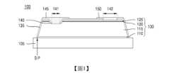
圖1係繪示根據本發明的第一態樣的發光裝置的圖。FIG. 1 is a diagram showing a light emitting device according to a first aspect of the present invention.
請參考圖1,根據第一態樣的發光裝置100可設置於生長基板105上。雖然圖1為了方便說明而僅繪示一個發光裝置100,但多個發光裝置可在生長基板105上被布置成彼此分離。發光裝置100可包含氮化物半導體結構130、環繞氮化物半導體結構130的外表面的鈍化圖案135、第一電極145以及第二電極150。氮化物半導體結構130可包含緩衝半導體層110、第一半導體層115、主動層120以及第二半導體層125。此外,氮化物半導體結構130可具有界定於其中的溝槽孔140,其中溝槽孔140延伸穿過第二半導體層125以及主動層120且使第一半導體層115之部分被露出。Referring to FIG. 1 , a
鈍化圖案135可覆蓋氮化物半導體結構130的外表面以及溝槽孔140的側表面。形成氮化物半導體結構130時,鈍化圖案135在乾蝕刻製程期間用以防止可能會發生於氮化物半導體結構的側表面130上的損毀,進而補充裝置的特性。鈍化圖案135被形成以具有非常薄的厚度。舉例來說,鈍化圖案135可具有100奈米(nm)至120奈米(nm)的厚度,且可被形成以具有不超過120 nm的厚度。The passivation pattern 135 may cover the outer surface of the
再者,鈍化圖案135可包含使第一半導體層115的表面之部分被露出的第一開放區域141,以及使第二半導體層125的表面之部分被露出的第二開放區域142。第一電極145接觸透過第一開放區域141所露出的第一半導體層115之部分,且第二電極150接觸透過第二開放區域142所露出的第二半導體層125之部分。第一電極145以及第二電極150可透過鈍化圖案135而彼此絕緣。Furthermore, the passivation pattern 135 may include a first
在一示例中,作為氮化物半導體結構130之最底部部分的緩衝半導體層110具有整個底表面可與生長基板105接觸的形狀。In one example, the
可藉由使用雷射剝離製程將分別包含氮化物半導體結構130的多個獨立的發光裝置100從生長基板105移除,以使彼此分離。然而,裂縫缺陷可能會發生於雷射剝離製程期間。舉例來說,鈍化圖案135能保護氮化物半導體結構130,且改善發光裝置的特性。此外,如上所述,鈍化圖案135被形成以具有100 nm至120 nm的薄的厚度。A plurality of independent
當鈍化圖案135的厚度太厚(例如,厚於120 nm)時,厚的鈍化圖案135可為雷射剝離製程期間裂縫開始的起點。鈍化圖案135的底表面S·P與生長基板105接觸。當在鈍化圖案135的底表面S·P與生長基板105接觸的同時裂縫產生時,從氮化物半導體結構130移除的鈍化圖案135之部分會成為殘留物。因裂縫而從氮化物半導體結構130移除的鈍化圖案135的殘留物可在後續製程中作為外來物質,且當發光裝置轉移至封裝基板時,殘留物可作為導致缺陷的原因,進而降低裝置的可靠性。When the thickness of the passivation pattern 135 is too thick (e.g., thicker than 120 nm), the thick passivation pattern 135 may be a starting point for cracks to start during the laser stripping process. The bottom surface S·P of the passivation pattern 135 is in contact with the
為了防止這樣的缺陷,鈍化圖案135被形成以具有適當的厚度,例如120 nm以下。然而,當鈍化圖案135的厚度變太薄時,在乾蝕刻製程中防止可能會發生於氮化物半導體結構130的側表面上的損毀有其限制。當損毀沒有被防止而是殘留在氮化物半導體結構130的側表面上時,大量不參與發光的電子與電洞的異常組合會發生於氮化物半導體結構130的外表面上。因此,發光面積可能會顯著地減少。在此情況下,即便施加相同電流,外部量子效率(EQE)仍降低,亮度(luminance)仍降低,且因此發光效率會大幅降低。In order to prevent such defects, the passivation pattern 135 is formed to have an appropriate thickness, for example, 120 nm or less. However, when the thickness of the passivation pattern 135 becomes too thin, there is a limit to preventing damage that may occur on the side surface of the
因此,在本發明的一態樣中,將描述能夠防止裂縫缺陷發生於雷射剝離製程期間以增加發光效率的發光裝置、包含發光裝置的顯示設備及其製造方法。這將於以下參照圖式來描述。Therefore, in one aspect of the present invention, a light emitting device capable of preventing crack defects from occurring during a laser lift-off process to increase light emitting efficiency, a display device including the light emitting device, and a manufacturing method thereof will be described below with reference to the drawings.
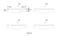
圖2A至圖2C係繪示根據本發明的第二態樣的發光裝置的圖。在這方面,圖2A係發光裝置的平面圖,且圖2B係沿著圖2A的線I-I'切的剖面圖。圖2C係繪示本發明的第二態樣的另一示例中的更包含光散射圖案的發光裝置的剖面圖。2A to 2C are diagrams showing a light emitting device according to the second aspect of the present invention. In this regard, FIG2A is a plan view of the light emitting device, and FIG2B is a cross-sectional view cut along line II' of FIG2A. FIG2C is a cross-sectional view showing a light emitting device further including a light scattering pattern in another example of the second aspect of the present invention.
請參考圖2A至圖2C,根據本發明的第二態樣的發光裝置200可包含氮化物半導體結構230、鈍化圖案235、第一電極245以及第二電極250。氮化物半導體結構230可設置於生長基板205上。發光裝置200可以指包含除了生長基板205之外的元件的裝置。2A to 2C , the
氮化物半導體結構230可包含緩衝半導體層210、第一半導體層215、主動層220以及第二半導體層225。氮化物半導體結構230的第一半導體層215可包含具有第一寬度W1的下部部分212,以及具有大於第一寬度W1的第二寬度W2的上部部分214。第一半導體層215可包含突出部。係藉由底切(undercutting)下部部分214來形成第一半導體層215的突出部。位於第一半導體層215之下的緩衝半導體層210可具有與第一半導體層215的下部部分212的第一寬度W1相同的寬度。再者,位於第一半導體層215之上的主動層220以及第二半導體層225中的每一者可具有小於第一半導體層215的上部部分214的第二寬度W2的寬度。因此,第一半導體層215的下部部分212可以指可包含與第一半導體層215的上部部分214的材料相同的材料的突出部,且可為與上部部分214一體成型的上部部分214的懸凸部分(或突出部)。根據本發明的一態樣的發光裝置200的第一半導體層215可包含從其的一個表面突出的突出部。The
舉例來說,如圖2B所示,氮化物半導體結構230可在剖面圖中具有「T」形形狀。For example, as shown in FIG. 2B , the
鈍化圖案235可具有覆蓋氮化物半導體結構230的上表面之部分以及外側面之部分的形狀。舉例來說,鈍化圖案235可具有環繞第一半導體層215的第二半導體層225、主動層220以及上部部分214中的每一者的外側面的形狀。因此,第一半導體層215的下部部分212的外側面可被曝露在發光裝置外部。鈍化圖案235可覆蓋氮化物半導體結構230的側表面,且不覆蓋第一半導體層215的突出部中將被露出的外側面。再者,鈍化圖案235可包含使第一半導體層215的表面之部分被露出的第一開放區域241,以及使第二半導體層225的表面之部分被露出的第二開放區域242。The
第一電極245可接觸透過第一開放區域241所露出的第一半導體層215之部分,且第二電極250可接觸透過第二開放區域242所露出的第二半導體層225之部分。第一電極245以及第二電極250可透過鈍化圖案235而彼此絕緣。The
作為氮化物半導體結構230之最下部的緩衝半導體層210具有整個底表面接觸生長基板205的形狀。在此情況下,緩衝半導體層210與第一半導體層215的下部部分212具有相同的寬度,且因此緩衝半導體層210以小於第二寬度W2的第一寬度W1的尺寸接觸生長基板205。再者,因為鈍化圖案235的底表面235b與生長基板205的表面以第一半導體層215的下部部分212的高度H1分離,所以鈍化圖案235不與生長基板205接觸。因此,可在雷射剝離製程中防止裂縫從鈍化圖案235發生。再者,因為鈍化圖案235不接觸生長基板205的表面且與生長基板205的表面分離,所以鈍化圖案235可在缺少第一半導體層215的下部部分212的結構中相較於鈍化圖案135具有更大的厚度。舉例來說,鈍化圖案235的厚度可大於120 nm。因此,鈍化圖案235可具有足以防止氮化物半導體結構230的側表面的損毀的厚度。在此情況下,第一半導體層215的下部部分212的高度H1小於第一半導體層215的高度。The
由於具有足夠的厚度的鈍化圖案235防止了因電漿而導致的氮化物半導體結構230的側表面的損毀,所以能抑制異常的電子-電洞結合,進而改善發光裝置200的發光效率。Since the
在另一示例中,如圖2C所示,光散射圖案255可進一步設置於第一半導體層215的下部部分212的外側面上。光散射圖案255可具有凹凸不平且不規則(或非平坦)的表面。形成於第一半導體層215的下部部分212的外側面上的光散射圖案255引發所發出的光的散射,進而改善發光裝置200的光提取效率。舉例來說,當沒有光散射圖案255時,構成氮化物半導體結構230的GaN基氮化物的折射率可約為2.4。在此情況下,會發生全內反射,且因此大量的光束可能會在其中熄滅,而可能會降低光提取效率。In another example, as shown in FIG. 2C , a
在這方面,於本發明的一態樣中,當第一半導體層215的下部部分212包含設置於其的外側面上的光散射圖案255時,光散射可能會重複發生於光散射圖案255的不規則表面上,而可增加發出至外部的光的量,且因此可減少全內反射。因此,增加了光發出至外部的光提取效率,進而改善發光裝置的效能。In this regard, in one aspect of the present invention, when the
氮化物半導體結構230可具有界定於其中的溝槽孔240,其中溝槽孔240延伸穿過第二半導體層225以及主動層220且使第一半導體層215之部分被露出。The
圖3係繪示根據本發明的第三態樣的發光裝置的圖。FIG. 3 is a diagram showing a light emitting device according to a third aspect of the present invention.
請參考圖3,發光裝置300可包含氮化物半導體結構330、鈍化圖案335、第一電極345以及第二電極350。氮化物半導體結構330可設置於生長基板305上。因為除了發光裝置300具有凸台(mesa)結構之外,根據本發明的第三態樣的發光裝置300與根據圖2A至圖2C的第二態樣的發光裝置相同,所以將描述其之間的差異,而相同的元件的描述可被省略。3 , the
氮化物半導體結構330可包含緩衝半導體層310、第一半導體層315、主動層320以及第二半導體層325。氮化物半導體結構330的第一半導體層315可包含具有第一寬度W3的下部部分312,以及具有大於第一寬度W3的第二寬度W4的上部部分314。氮化物半導體結構330的主動層320以及第二半導體層325設置於第一半導體層315的頂面的一側上。在與其頂面的一側相對的頂面的另一側中,第一半導體層315的上部部分314的頂面之部分因凸台蝕刻而被露出。第一半導體層的上部部分314的頂面因凸台蝕刻而具有階梯結構(step)。第一半導體層315包含下部部分312以及上部部分314。The
作為氮化物半導體結構330之最下部的緩衝半導體層310可與第一半導體層315的下部部分312的第一寬度W3具有相同的寬度。位於第一半導體層315之上的主動層320以及第二半導體層325中的每一者具有比第一半導體層315的下部部分312的第一寬度W3還大的寬度,且具有比第一半導體層315的上部部分314的第二寬度W4還小的寬度。因此,第一半導體層315的下部部分312可作為包含與第一半導體層315的上部部分314的材料相同的材料的突出部,且與其一體成型,並從上部部分314突出。The
除了第一半導體層315的下部部分312的外側面之外,鈍化圖案335可具有覆蓋氮化物半導體結構330所露出的表面的形狀。舉例來說,鈍化圖案335可具有環繞第一半導體層315的第二半導體層325、主動層320以及上部部分314中的每一者的外側面的形狀。因此,第一半導體層315的下部部分312的外側面可被曝露在外部。再者,鈍化圖案335可包含使因凸台蝕刻而被露出的第一半導體層315的頂面之部分被露出的第一開放區域341,以及使第二半導體層325的頂面之部分被露出的第二開放區域342。The
在第二電極350可接觸透過第二開放區域342所露出的第二半導體層325之部分的同時,第一電極345可接觸透過第一開放區域341所露出的第一半導體層315之部分。第一電極345以及第二電極350可透過鈍化圖案335而彼此絕緣。While the
因為作為氮化物半導體結構330的最下部的緩衝半導體層310與第一半導體層315的下部部分312具有相同的寬度,所以緩衝半導體層310以相同於第一寬度W3的尺寸接觸生長基板305。再者,因為鈍化圖案335的底表面與生長基板305的頂面以第一半導體層315的下部部分312的高度H2分離,所以鈍化圖案335的底表面不與生長基板305接觸。因此,可在雷射剝離製程期間防止裂縫從鈍化圖案335發生。再者,鈍化圖案335具有足以防止氮化物半導體結構330的側表面的損毀的厚度。這能抑制異常的電子-電洞結合,進而增加發光效率。在此情況下,第一半導體層315的下部部分312的高度H2小於第一半導體層315的高度。Because the
再者,光散射圖案255可進一步設置於第一半導體層315的下部部分312的外側面上(繪示於圖2C)。光散射圖案255可具有凹凸不平且不規則(或非平坦)的表面。具有不規則表面的光散射圖案255可能會引發所發出的光的散射,藉以改善發光裝置300的光提取效率。Furthermore, a
圖4係繪示根據本發明的第四態樣的發光裝置的圖。FIG. 4 is a diagram showing a light emitting device according to a fourth aspect of the present invention.
請參考圖4,發光裝置400可包含氮化物半導體結構430、鈍化圖案435以及墊部450。氮化物半導體結構430可設置於生長基板405上。因為根據本發明的第四態樣的發光裝置400不同於根據圖2A至圖2C的第二態樣的發光裝置之處在於發光裝置400具有垂直的結構,所以將描述其之間的差異。4 , the
氮化物半導體結構430可包含緩衝半導體層410、第一半導體層415、主動層420以及第二半導體層425。氮化物半導體結構430的第一半導體層415可包含具有第一寬度W5的下部部分412,以及具有大於第一寬度W5的第二寬度W6的上部部分414。在氮化物半導體結構430中,第一半導體層415的上部部分414、主動層420以及第二半導體層425可依序地設置於下部部分412上。在氮化物半導體結構430中,主動層420以及第二半導體層425中的每一者的外側面可沿著傾斜線與第一半導體層415的上部部分414的外側面對齊。舉例來說,氮化物半導體結構430的寬度可隨氮化物半導體結構430從第一半導體層415的上部部分414朝向第二半導體層425延伸而逐漸地減少。在此情況下,氮化物半導體結構430的外側面可為傾斜側表面。舉例來說,第一半導體層415的上部部分414可具有相對於其底表面具有預設傾角θ的傾斜側表面。氮化物半導體結構430可在剖面圖中具有「T」形形狀。The
作為氮化物半導體結構430的最下部的緩衝半導體層410可具有與第一半導體層415的下部部分412的寬度W5相同的寬度。位於第一半導體層415之上的主動層420以及第二半導體層425中的每一者可具有比第一半導體層415的下部部分412的第一寬度W5還大的寬度。The
除了第一半導體層415的下部部分412的外側面之外,鈍化圖案435可具有覆蓋氮化物半導體結構430所露出的表面的形狀。舉例來說,鈍化圖案435可具有環繞第一半導體層415的第二半導體層425、主動層420以及上部部分414中的每一者的外側面的形狀。因此,第一半導體層415的下部部分412的外側面可被露出。再者,鈍化圖案435可包含使第二半導體層425的頂面之部分被露出的開放區域。墊部450可被設置成與透過開放區域所露出的第二半導體層425的頂面之部分接觸。The
因為作為氮化物半導體結構430的最下部的緩衝半導體層410與第一半導體層415的下部部分412具有相同的寬度,所以緩衝半導體層410以相同於第一寬度W5的尺寸接觸生長基板405。再者,鈍化圖案435的底表面與生長基板405的頂面以第一半導體層415的下部部分412的高度分離,且因此不與生長基板405接觸。這可在雷射剝離製程期間防止從鈍化圖案435發生的裂縫。再者,鈍化圖案435具有足以保護氮化物半導體結構430的側表面不受可能會發生於乾蝕刻製程期間的損毀影響的厚度。因此,能抑制異常的電子-電洞結合,且因此能增加發光裝置400的發光效率。在另一示例中,光散射圖案255(繪示於圖2C)可進一步設置於第一半導體層415的下部部分412的外側面上。Because the
圖5係繪示根據本發明的一態樣的顯示設備的圖。FIG. 5 is a diagram showing a display device according to one aspect of the present invention.
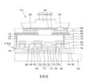
請參考圖5,根據本發明的一態樣的顯示設備包含發光裝置結合至封裝基板P-SUB上的配置。舉例來說,發光裝置可被體現為本發明的第二態樣的發光裝置200。5 , a display device according to one aspect of the present invention includes a configuration in which a light emitting device is combined with a package substrate P-SUB. For example, the light emitting device can be embodied as a
如上所述,發光裝置200可包含氮化物半導體結構230、鈍化圖案235、第一電極245以及第二電極250。再者,氮化物半導體結構230可包含緩衝半導體層210、第一半導體層215、主動層220以及第二半導體層225,且可在剖面圖中具有「T」形形狀。舉例來說,氮化物半導體結構230可具有於其中具有第一寬度W1的第一半導體層215的下部部分從其上部部分向下突出的形狀。As described above, the
用於驅動發光裝置的多個電路元件設置於包含基底基板700的封裝基板P-SUB中。具體來說,薄膜電晶體TFT設置於封裝基板P-SUB中。薄膜電晶體TFT可包含形成於基底基板700上的半導體層720、位於半導體層720上的閘極電極730、位於半導體層720和閘極電極730之間的閘極絕緣層725,以及源極和汲極電極760。緩衝層705以及阻光膜710可設置於基底基板700和半導體層720之間。A plurality of circuit elements for driving the light emitting device are disposed in a package substrate P-SUB including a
緩衝層705能防止雜質或濕氣從基底基板700擴散至薄膜電晶體TFT。阻光層710用以防止光進入半導體層720。第一層間絕緣層715可設置於緩衝層705、阻光層710和半導體層720之間。The
閘極電極730可設置於閘極絕緣層725上,以與半導體層720重疊。第二層間絕緣層735以及第三層間絕緣層745可依序地設置於閘極電極730上。The
多個連接線路740可設置於第二層間絕緣層735上。第三層間絕緣層745可位於第二層間絕緣層735上,且可覆蓋這些連接線路740。在閘極電極730插設於源極和汲極電極760之間的同時,源極和汲極電極760可設置於第三層間絕緣層745上。源極和汲極接觸孔750可延伸穿過第三層間絕緣層745、第二層間絕緣層735以及閘極絕緣層725,以分別使半導體層720的源極以及汲極區域之部分被露出。源極和汲極接觸孔750可被填充有導電材料或金屬材料,以分別形成源極和汲極接觸處755。源極和汲極電極760中的每一者可經由源極和汲極接觸處755中的每一者電性連接於半導體層720以及至少一連接線路740。在此情況下,在源極和汲極電極760中的每一者的一側可連接於連接線路740的同時,源極和汲極電極760中的每一者的另一側可連接於半導體層720。連接線路740可包含例如共用電壓線路等的電壓線路。A plurality of
保護層765設置於第三層間絕緣層745上。保護層765被形成以覆蓋源極和汲極電極760。平坦化膜770設置於保護層765上。平坦化膜770可足夠厚,以使由下層(underlying)電路元件導致的階梯狀(stepped)上表面平坦化。A
第一連接電極775以及第二連接電極780設置於平坦化膜770上。第一連接電極775以及第二連接電極780中的每一者可經由導電接觸處777連接於第二層間絕緣層735上所設置的連接線路740。為此,接觸孔776可延伸穿過平坦化膜770、保護層765以及第三層間絕緣層745,且可被填充有導電材料或金屬材料,以形成導電接觸處777。導電接觸處777可接觸且電性連接於第一連接電極775以及第二連接電極780中的每一者的底表面。The
界定發光裝置200將被放置的位置的固持區域792可位於第一連接電極775和第二連接電極780之間。在這方面,第一連接電極775可電性連接於連接線路740。再者,第二連接電極780可電性連接於薄膜電晶體TFT。The holding
在這方面,發光裝置200包含從其上部部分突出的第一半導體晶片215的下部部分212(繪示於圖2A至圖2C)。再者,第一半導體晶片215的突出的下部部分212可被對齊,使得突出的下部部分212插入發光裝置200將被放置的固持區域792中。封裝基板P-SUB可包含固持區域792。作為突出部的第一半導體晶片215的下部部分212可被接收於固持區域792中。因此,當將多個發光裝置200轉移至封裝基板P-SUB上時,會有容易將發光裝置與目標區域在封裝基板P-SUB上對齊的功效。In this regard, the
覆蓋膜820設置於發光裝置200以及平坦化膜770上。覆蓋膜820可被設置,以環繞發光裝置200的外側面。舉例來說,覆蓋膜820可由樹脂製成。第一線路電極800以及第二線路電極805可設置於覆蓋膜820上。第一線路電極800以及第二線路電極805可分別將連接於發光裝置200的第一半導體層215的第一電極245以及連接於第二半導體層225的第二電極250電性連接於設置於封裝基板P-SUB中的電路元件。第一電極245以及第二電極250可經由延伸穿過覆蓋膜820的墊部接觸處815a、815b分別電性連接於設置於封裝基板P-SUB中的多個電路元件,以分別連接於第一線路電極800以及第二線路電極805。在這方面,在第二線路電極805可經由填滿通孔810中的第二墊部接觸處815b電性連接於第二連接電極780的同時,第一線路電極800可經由第一墊部接觸處815a電性連接於第一連接電極775。The
第一線路電極800以及第二線路電極805中的每一者可由例如Au、W、Pt、Si、Ir、Ag、Cu、Ni、Ti、Cr,或上述金屬中至少兩者的合金的金屬材料製成。再者,第一線路電極800以及第二線路電極805中的每一者可包含例如氧化銦錫(ITO)以及氧化銦鋅(IZO)的透明金屬氧化物。本發明並不以此為限。Each of the
在另一示例中,可以覆晶法(flip-chip scheme)來將發光裝置安裝至封裝基板上。這將於以下參照圖式來描述。In another example, the light emitting device may be mounted on the package substrate using a flip-chip scheme, which will be described below with reference to the drawings.
圖6係繪示根據本發明的另一態樣的顯示設備的圖。因為圖6所示的發光裝置以及封裝基板中的每一者與圖5中的發光裝置以及封裝基板中的每一者包含相同的元件,所以將於以下描述其之間的差異。Fig. 6 is a diagram showing a display device according to another aspect of the present invention. Since each of the light emitting device and the package substrate shown in Fig. 6 includes the same elements as each of the light emitting device and the package substrate in Fig. 5, the differences therebetween will be described below.
請參考圖6,根據本發明的另一態樣的顯示設備包含發光裝置結合至封裝基板P-SUB上的配置。發光裝置可被體現為本發明的第二態樣的發光裝置200。在此情況下,發光裝置200具有其第一電極245以及第二電極250分別面對封裝基板P-SUB的第一連接電極775以及第二連接電極780的覆晶狀(flip-chip shape)。6, a display device according to another aspect of the present invention includes a configuration in which a light emitting device is combined with a package substrate P-SUB. The light emitting device can be embodied as a
發光裝置200以及封裝基板P-SUB可經由例如導電球的導電黏合材料825而彼此結合。當導電黏合材料825被體現為導電球時,黏合樹脂層830可設置於發光裝置200和封裝基板P-SUB之間,以固定導電球。The
圖7係繪示根據本發明的又再另一態樣的顯示設備的圖。在這方面,繪示於圖7中的發光裝置400與根據本發明的第四態樣的發光裝置包含相同的配置。Fig. 7 is a diagram showing a display device according to yet another aspect of the present invention. In this regard, the
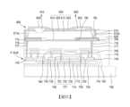
請參考圖7,根據本發明的又再另一態樣的顯示設備包含發光裝置400結合至封裝基板P-SUB上的配置。Please refer to FIG. 7 , a display device according to yet another aspect of the present invention includes a configuration in which a
發光裝置400可包含氮化物半導體結構430、鈍化圖案435、第一電極445以及第二電極450。氮化物半導體結構430可包含緩衝半導體層410、第一半導體層415、主動層420以及第二半導體層425。氮化物半導體結構430的第一半導體層415可包含具有第一寬度W5的下部部分412(繪示於圖4),以及具有大於第一寬度W5的第二寬度W6的上部部分414。換言之,氮化物半導體結構430可具有於其中具有第一寬度W5的第一半導體層415的下部部分412從上部部分414向下突出的形狀。The
用於驅動發光裝置晶片的多個電路元件設置於包含基底基板700的封裝基板P-SUB中。具體來說,薄膜電晶體TFT設置於封裝基板P-SUB中。薄膜電晶體TFT可包含形成於基底基板700上的半導體層720、位於半導體層720上的閘極電極730、位於半導體層720和閘極電極730之間的閘極絕緣層725,以及源極和汲極電極760。緩衝層705以及阻光膜710可設置於基底基板700和半導體層720之間。A plurality of circuit elements for driving the light emitting device chip are disposed in a package substrate P-SUB including a
緩衝層705能防止雜質或濕氣從基底基板700擴散至薄膜電晶體TFT。阻光層710用以防止光進入半導體層720。第一層間絕緣層715可設置於緩衝層705、阻光層710和半導體層720之間。The
閘極電極730可設置於閘極絕緣層725上,以與半導體層720重疊。第二層間絕緣層735以及第三層間絕緣層745可依序地設置於閘極電極730上。The
多個連接線路740可設置於第二層間絕緣層735上。第三層間絕緣層745可位於第二層間絕緣層735上,且可覆蓋這些連接線路740。在閘極電極730插設於源極和汲極電極760之間的同時,源極和汲極電極760可設置於第三層間絕緣層745上。源極和汲極接觸孔750可延伸穿過第三層間絕緣層745、第二層間絕緣層735以及閘極絕緣層725,以分別使半導體層720的源極和汲極區域之部分被露出。源極和汲極接觸孔750可被填充有導電材料或金屬材料,以分別形成源極和汲極接觸處755。源極和汲極電極760中的每一者可經由源極和汲極接觸處755中的每一者電性連接於半導體層720以及至少一連接線路740。在此情況下,在源極和汲極電極760中的每一者的另一側可連接於連接線路740的同時,源極和汲極電極760中的每一者的一側可連接於半導體層720。連接線路740可包含例如共用電壓線路的電壓線路。A plurality of
保護層765設置於第三層間絕緣層745上。保護層765被形成以覆蓋源極和汲極電極760。平坦化膜770設置於保護層765上。平坦化膜770可足夠厚,以使由下層電路元件導致的階梯狀上表面平坦化。A
第一連接電極775以及第二連接電極780設置於平坦化膜770上。第一連接電極775以及第二連接電極780中的每一者可經由導電接觸處777連接於第二層間絕緣層735上所設置的連接線路740。為此,接觸孔776可延伸穿過平坦化膜770、保護層765以及第三層間絕緣層745,且可被填充有導電材料或金屬材料,以形成導電接觸處777。導電接觸處777可接觸且電性連接於第一連接電極775以及第二連接電極780中的每一者的底表面。在這方面,第一連接電極775可電性連接於連接線路740。再者,第二連接電極780可電性連接於薄膜電晶體TFT。The
上部絕緣層790可形成於第二連接電極780之下。界定發光裝置400將被放置的位置的固持區域792可被上部絕緣層790界定,且可設置於第二連接電極780上。The upper insulating
發光裝置400包含第一半導體晶片415的突出的下部部分412(繪示於圖4)。此外,第一半導體晶片415的突出的下部部分412可插入發光裝置400將被放置的固持區域792中。因此,當將多個發光裝置400轉移至封裝基板P-SUB上時,會有容易將發光裝置與目標區域在封裝基板P-SUB上對齊的功效。The
發光裝置400以及封裝基板P-SUB可經由例如導電球的導電黏合材料825而彼此結合。當導電黏合材料825被體現為導電球時,黏合樹脂層830可設置於發光裝置200和封裝基板P-SUB之間,以固定導電球。The
在具有垂直的結構的發光裝置400中,多個墊部沿著垂直方向被放置成彼此相對。舉例來說,在與第一電極445相對的第二電極450接觸第二半導體層425的同時,第一電極445接觸緩衝半導體層410以及第一半導體層415。線路電極800可部分地設置於第二電極450上,且可經由多個導電接觸處777之中的一者電性連接於多個連接線路740之中的一者。線路電極800可經由墊部接觸處815電性連接於第一連接電極775。再者,第一電極445可經由導電黏合材料825電性連接於第二連接電極780。第二連接電極780可經由導電接觸處777電性連接於另一連接線路740。In the
在這方面,發光裝置400包含第一半導體晶片415的突出的下部部分412(繪示於圖4)。再者,第一半導體晶片415的突出的下部部分412可與固持區域792對齊,且可插入固持區域792中。因此,即便多個發光裝置400被轉移至封裝基板P-SUB上時,仍會有容易將發光裝置與目標區域在封裝基板P-SUB上對齊的功效。In this regard, the
圖8至圖21係用於繪示設置有根據本發明的一態樣的發光裝置的顯示設備的製造方法的圖。8 to 21 are diagrams for illustrating a method for manufacturing a display device provided with a light-emitting device according to one embodiment of the present invention.
首先請參考圖8至圖10,遮罩圖案605形成於生長基板600上。為此,遮罩材料層形成於生長基板600的整個表面上,且圖案化製程被進行,以選擇性地移除遮罩材料層,以形成遮罩圖案605。圖9係圖8或圖10沿著線II-II'切的剖面圖。First, referring to Figures 8 to 10, a
生長基板600可由例如藍寶石、矽(Si)、碳化矽(SiC)以及砷化鎵(GaAs)的材料製成。然而,本發明並不以此為限。遮罩材料層可包含其上不生長氮化物基半導體的材料。再者,遮罩材料層可包含可藉由使用濕蝕刻劑容易移除的材料。舉例來說,遮罩材料層由包含矽氧化物或氧化銦錫(ITO)的絕緣材料製成。The
遮罩圖案605包含沿著作為生長基板600的第一方向的Y軸方向延伸且沿著作為相交於第一方向的第二方向的X軸方向彼此分離的多個子圖案605-1、605-2。因此,這些子圖案605-1、605-2中的每一者具有條紋形狀。The
舉例來說,構成一個遮罩圖案605a的第一子圖案605-1以及被設置成相鄰於第一子圖案605-1的第二子圖案605-2可具有相同的線寬度a。第二子圖案605-2可與第一子圖案605-1以預設距離d分離。作為第一子圖案605-1的線寬度a、第二子圖案605-2的線寬度a,以及第一子圖案605-1和第二子圖案605-2之間的距離d的加總的尺寸b可為將於之後形成的一個發光裝置的尺寸。換言之,設置有一個發光裝置的區域可對應到包含第一子圖案605-1以及第二子圖案605-2的遮罩圖案605a。For example, a first sub-pattern 605-1 constituting a
再者,可沿著作為生長基板600的第二方向的X軸方向重複布置多個第一子圖案605-1以及多個第二子圖案605-2。對應一個發光裝置的遮罩圖案605a以及對應一個發光裝置且相鄰於遮罩圖案605a的遮罩圖案605b彼此可以間隔s分離。在以下圖式中,遮罩圖案將統稱為605。Furthermore, a plurality of first sub-patterns 605-1 and a plurality of second sub-patterns 605-2 may be repeatedly arranged along the X-axis direction as the second direction of the
請參考圖10,遮罩圖案605可被形成以包含多個格子形狀,各格子具有界定於其中的空間SA。根據本發明的一態樣,一個格子狀的遮罩圖案605可具有數微米(µm)至數十微米的寬度以及長度。將放置發光裝置C1、C2、C3、C4中的每一者的區域可被界定,以包含界定成格子形狀的空間SA。10 , the
請參考圖11,係在已形成有遮罩圖案605的生長基板600上進行磊晶(epitaxy)製程。磊晶製程可被理解為在某種晶體的表面上以特定取向關係生長材料的製程。為了形成微型LED基發光裝置的氮化物半導體結構,GaN基化合物半導體應沉積於生長基板600的頂面上。此時,各層體系基於下層層體的結晶度來生長。Please refer to FIG. 11 , which shows an epitaxy process on a
當進行了磊晶製程時,緩衝半導體材料層610a、第一半導體材料層615a、主動材料層620a以及第二半導體材料層625a可依序地在彼此相鄰的遮罩圖案的子圖案605-1、605-2之間的區域中生長,且在生長基板600上生長。在這方面,設置有遮罩圖案605的區域包含在磊晶製程期間其上不生長半導體層的材料,且因此緩衝半導體材料層610a、第一半導體材料層615a、主動材料層620a以及第二半導體材料層625a可選擇性地僅生長於除了遮罩圖案605之外的殘留的區域中。When the epitaxial process is performed, the buffer semiconductor material layer 610a, the first semiconductor material layer 615a, the active material layer 620a, and the second semiconductor material layer 625a may be sequentially grown in the region between the sub-patterns 605-1 and 605-2 of the mask pattern adjacent to each other, and grown on the
作為最下部的層體的緩衝半導體材料層610a可被形成以包含未摻雜的氮化物半導體。舉例來說,氮化物半導體可為GaN基半導體材料。第一半導體材料層615a形成於緩衝半導體材料層610a的頂面上。第一半導體材料層615a可包含含有第一導電型雜質的氮化物半導體。舉例來說,第一導電型雜質可包含N型雜質。第一半導體材料層615a的氮化物半導體可由包含GaN、AlGaN、InGaN或AlInGaN的GaN基半導體材料製成。第一半導體材料層615a中用於摻雜的N型雜質可包含矽(Si)、鍺(Ge)、硒(Se)、碲(Te)或碳(C)。本發明並不以此為限。The buffer semiconductor material layer 610a as the lowermost layer may be formed to include an undoped nitride semiconductor. For example, the nitride semiconductor may be a GaN-based semiconductor material. The first semiconductor material layer 615a is formed on the top surface of the buffer semiconductor material layer 610a. The first semiconductor material layer 615a may include a nitride semiconductor containing a first conductive type impurity. For example, the first conductive type impurity may include N-type impurities. The nitride semiconductor of the first semiconductor material layer 615a may be made of a GaN-based semiconductor material including GaN, AlGaN, InGaN or AlInGaN. The N-type impurities used for doping in the first semiconductor material layer 615a may include silicon (Si), germanium (Ge), selenium (Se), tellurium (Te) or carbon (C). The present invention is not limited thereto.
第一半導體材料層615a會生長,以填滿多個子遮罩圖案之間的空間,且接著填滿整個空間,且接著能向上生長至垂直位準,以具有預設厚度。舉例來說,第一半導體材料層615a可包含填滿多個子遮罩圖案605之間的空間的下部部分612a。舉例來說,第一半導體材料層615可包含下部部分612a,以及形成於下部部分以及遮罩圖案605上的上部部分614a。The first semiconductor material layer 615a grows to fill the space between the plurality of sub-mask patterns, and then fills the entire space, and then can grow upward to a vertical level to have a preset thickness. For example, the first semiconductor material layer 615a may include a lower portion 612a filling the space between the plurality of
主動材料層620a位於第一半導體材料層615a的頂面上。主動材料層620a可為用於基於電子以及電洞的結合而發光的層體。主動材料層620a包含具有井層(well layer)以及相較於井層具有更高能帶間隙(band gap)的障壁層的多量子井(MQW)結構。舉例來說,主動材料層620a可包含作為井層的InGaN層以及作為障壁層的AlGaN層。然而,其材料並不以此為限。The active material layer 620a is located on the top surface of the first semiconductor material layer 615a. The active material layer 620a can be a layer for emitting light based on the combination of electrons and holes. The active material layer 620a includes a multi-quantum well (MQW) structure having a well layer and a barrier layer having a higher band gap than the well layer. For example, the active material layer 620a can include an InGaN layer as a well layer and an AlGaN layer as a barrier layer. However, the material is not limited thereto.
第二半導體材料層625a形成於主動材料層620a上。第二半導體材料層625a可包含含有第二導電型雜質的氮化物半導體。舉例來說,第二導電型雜質可包含P型雜質。第二半導體材料層625a的氮化物半導體可由包含GaN、AlGaN、InGaN或AlInGaN的GaN基半導體材料製成。包含於第二半導體材料層625a中的P型雜質可包含鎂(Mg)、鋅(Zn)或鈹(Be)。The second semiconductor material layer 625a is formed on the active material layer 620a. The second semiconductor material layer 625a may include a nitride semiconductor containing a second conductivity type impurity. For example, the second conductivity type impurity may include a P-type impurity. The nitride semiconductor of the second semiconductor material layer 625a may be made of a GaN-based semiconductor material including GaN, AlGaN, InGaN, or AlInGaN. The P-type impurity included in the second semiconductor material layer 625a may include magnesium (Mg), zinc (Zn), or curium (Be).
在本發明的一態樣中,描述了第一半導體材料層615a以及第二半導體材料層625a分別包含含有N型雜質的氮化物半導體以及含有P型雜質的氮化物半導體之示例。然而,本發明並不以此為限。在另一示例中,第一半導體材料層615a以及第二半導體材料層625a可分別包含含有P型雜質的氮化物半導體以及含有N型雜質的氮化物半導體。In one embodiment of the present invention, an example is described in which the first semiconductor material layer 615a and the second semiconductor material layer 625a include a nitride semiconductor containing N-type impurities and a nitride semiconductor containing P-type impurities, respectively. However, the present invention is not limited thereto. In another example, the first semiconductor material layer 615a and the second semiconductor material layer 625a may include a nitride semiconductor containing P-type impurities and a nitride semiconductor containing N-type impurities, respectively.
隨後地,在後續圖案化製程中保護下層層體的蝕刻遮罩627形成於第二半導體材料層625a上。蝕刻遮罩627可被形成以具有界定於其中的開口,開口使第二半導體材料層625a的表面中與將形成有氮化物半導體結構的部分不同的其他部分被露出。Subsequently, an etching mask 627 for protecting the underlying layer in a subsequent patterning process is formed on the second semiconductor material layer 625a. The etching mask 627 may be formed to have an opening defined therein, the opening exposing other portions of the surface of the second semiconductor material layer 625a than the portion where the nitride semiconductor structure is to be formed.
請參考圖12,可藉由使用蝕刻遮罩627使第二半導體材料層625a、主動材料層620a、第一半導體材料層615a以及緩衝半導體層610a圖案化(見圖11),使得多個氮化物半導體結構630形成於生長基板600上且彼此分離。可以乾蝕刻方案來進行圖案化製程。可藉由使用反應氣體的感應耦合電漿-反應性離子蝕刻(inductively coupled plasma-reactive ion etch,ICP-RIE)來執行乾蝕刻方案。可藉由圖案化製程依序地蝕刻透過蝕刻遮罩627的開口所露出的部分。圖案化製程能繼續,使得生長基板600的表面被露出。接著,相鄰的多個氮化物半導體結構630可彼此分離。Referring to FIG. 12 , the second semiconductor material layer 625a, the active material layer 620a, the first semiconductor material layer 615a, and the buffer semiconductor layer 610a can be patterned (see FIG. 11 ) using an etching mask 627, so that a plurality of
由圖案化製程所形成的多個氮化物半導體結構630中的每一者可包含緩衝半導體層610、第一半導體層615、主動層620以及第二半導體層625。在這方面,第一半導體層615可包含位於多個子遮罩圖案605之間且具有第一寬度的下部部分612,以及從下部部分612朝向遮罩圖案605的上表面延伸且具有大於下部部分612的第一寬度的第二寬度的上部部分614。因此,氮化物半導體結構630可在剖面圖中具有「T」形形狀。接著,移除蝕刻遮罩627。Each of the plurality of
請參考圖13以及圖14,溝槽孔640形成於氮化物半導體結構630中。在這方面,圖13係圖14的俯視圖。圖14係沿著圖13的線III-III'截切的剖面圖。可藉由使用蝕刻製程來形成溝槽孔640。溝槽孔640可延伸穿過作為氮化物半導體結構630之最頂部的第二半導體層625以及主動層620,且可具有具備底表面以及側牆的溝槽形狀,所述溝槽形狀被界定於第一半導體層615中。可透過溝槽孔640的底表面使第一半導體層615被露出。13 and 14, a
隨後地,形成了覆蓋包含溝槽孔640的氮化物半導體結構630的外表面的鈍化圖案635。鈍化圖案635可包含絕緣材料。在一示例中,鈍化圖案635可包含矽氧化物(SiOx)。然而,本發明並不以此為限,且可將具有絕緣性質的材料應用為其材料。Subsequently, a
因為鈍化圖案635被形成以覆蓋溝槽孔640中除了底表面之外的側牆,所以溝槽孔640的底表面可作為使第一半導體層615的表面被露出的第一開放區域641。再者,鈍化圖案635可具有界定於其中的第二開放區域642,第二開放區域642在與第一開放區域641分離的位置使第二半導體層625的表面之部分被露出。Since the
鈍化圖案635用以改善發光裝置的特性。舉例來說,氮化物半導體結構630的側表面可能會在乾蝕刻製程期間被電漿損毀,以使相鄰的多個氮化物半導體結構630彼此分離。鈍化圖案635用以保護氮化物半導體結構630的側表面使其不損毀。再者,鈍化圖案635用以將於之後形成的第一電極以及第二電極彼此電性絕緣。The
鈍化圖案635係用於保護氮化物半導體結構630且改善發光裝置的特性的必要部件。然而,如圖1所示,鈍化圖案635具有鈍化圖案635應被形成以具有100 nm至120 nm的小厚度之限制。當鈍化圖案135(繪示於圖1)被形成以具有大於120 nm的厚度時,厚的鈍化圖案635作為雷射剝離製程期間裂縫開始的起點。再者,具有裂縫的鈍化圖案135中從氮化物半導體結構移除的殘留物在後續製程中作為異物,因而在發光裝置轉移至封裝基板時可作為導致缺陷的原因。The
然而,在本發明的一態樣中,遮罩圖案605設置於生長基板600和緩衝半導體層610之間,使得生長基板605和緩衝半導體層610之間的接觸區域能減少設置有遮罩圖案605的區域的寬度。再者,因為遮罩圖案605設置於鈍化圖案635和生長基板600之間,所以鈍化圖案635可不與生長基板600接觸。換言之,鈍化圖案635的底表面與生長基板600的頂面分離。However, in one aspect of the present invention, the
因此,可移除在雷射剝離製程中施加有雷射的鈍化圖案635之部分,進而防止裂縫從鈍化圖案635開始。因此,鈍化圖案635可在缺少第一半導體層615的下部部分612的結構中相較於鈍化圖案具有更大的厚度。舉例來說,鈍化圖案635的厚度可大於120 nm。因此,鈍化圖案635可具有足以防止氮化物半導體結構630的側表面的損毀的厚度,而可改善發光裝置的特性。在此情況下,第一半導體層615的下部部分612的高度小於第一半導體層615的上部部分614的高度。Therefore, the portion of the
在形成鈍化圖案635之後,可在接觸第一開放區域641的同時,於鈍化圖案635的上表面之部分上形成沿著其延伸的第一電極645。再者,可在接觸第二開放區域642的同時,於鈍化圖案635的上表面之另一部分上形成沿著其延伸的第二電極650。After forming the
請參考圖15,蝕刻終止圖案653形成於氮化物半導體結構630上。蝕刻終止圖案653可被形成以具有足以覆蓋環繞氮化物半導體結構630的外表面的鈍化圖案635的厚度。如圖15所示,蝕刻終止圖案653可被形成以與氮化物半導體結構630具有相同的寬度。在一示例中,可藉由施加光阻材料並對其進行曝光以及顯影製程來形成蝕刻終止圖案653。15 , an
因為蝕刻終止圖案653選擇性地僅形成於設置有氮化物半導體結構630的位置,所以蝕刻終止圖案653可包含在俯視圖中選擇性地使遮罩圖案605被露出的開放區域。Since the
請參考圖16,移除位於氮化物半導體結構630之下的遮罩圖案605(繪示於圖15)。可藉由在生長基板上進行濕蝕刻製程來移除遮罩圖案605。可藉由使用有彼此混合的氫氟酸(HF)以及氟化銨(NH4F)的緩衝氧化物蝕刻劑(Buffered Oxide Etchant,BOE)溶液,或包含氫氟酸的濕蝕刻劑來進行濕蝕刻製程。Referring to FIG. 16 , the mask pattern 605 (shown in FIG. 15 ) located below the
因為氮化物半導體結構630被蝕刻終止圖案653覆蓋,所以在氮化物半導體結構630被濕蝕刻劑影響的同時,可選擇性地僅移除遮罩圖案605。因為係選擇性地移除遮罩圖案605,所以可使第一半導體層615的下部部分612的外側面被露出。接著,移除蝕刻終止圖案653。在以下圖式中,包含下部部分612以及上部部分614的第一半導體層615將在圖式中被繪示為單一元件。Because the
在另一示例中,如圖17所示,遮罩圖案可部分地殘留於第一半導體層615的下部部分612的外側面上,且因此可作為光散射圖案655。光散射圖案655可具有凹凸不平且不規則的表面。舉例來說,可藉由調整在濕蝕刻製程中施加濕蝕刻劑的時間來形成光散射圖案655的不規則的表面。舉例來說,可控制濕蝕刻劑供應時間,使得遮罩圖案不被完全地移除,但部分地殘留於第一半導體層615的下部部分612的外側面上。設置於第一半導體層615的下部部分612的側表面上的光散射圖案655引發所發出的光的散射,進而改善發光裝置的光提取效率。舉例來說,當沒有光散射圖案255時,構成氮化物半導體結構的GaN基氮化物的折射率可為2.4。在此情況下,折射率具有高的值,從而發生全內反射,且因此大量的光束在其中熄滅,因而能降低光提取效率。In another example, as shown in FIG. 17 , the mask pattern may partially remain on the outer side surface of the
在這方面,於本發明的一態樣中,光散射圖案655設置於第一半導體層615的下部部分612的側表面上,使得光散射重複發生於光散射圖案655的不規則的表面上。因此,能增加發出至外部的光的量,且因此能減少全內反射。因此,可增加光發出至外部的光提取效率,進而改善發光裝置的效能。In this regard, in one aspect of the present invention, the
請參考圖18,從氮化物半導體結構630移除生長基板600,使得獨立的發光裝置660a、660b、660c、660d彼此分離。在此情況下,可在雷射剝離(LLO)製程中藉由使用雷射來移除生長基板600。當因此彼此分離的獨立的發光裝置660a、660b、660c、660d接著被轉移至顯示設備的封裝基板時,一個發光裝置能作為一個像素。18 , the
請參考圖19,製備封裝基板P-SUB,且接著多個發光裝置660被轉移至封裝基板P-SUB上。在發光裝置660被接附至載體基板C-SUB的同時,發光裝置660可移至封裝基板。發光裝置660可在封裝基板P-SUB的第一連接電極775和第二連接電極780之間與固持區域792對齊。19, a package substrate P-SUB is prepared, and then a plurality of light emitting
用於驅動發光裝置的多個電路元件設置於包含基底基板700的封裝基板P-SUB中。具體來說,薄膜電晶體TFT設置於封裝基板P-SUB中。薄膜電晶體TFT可包含形成於基底基板700上的半導體層720、位於半導體層720上的閘極電極730、位於半導體層720和閘極電極730之間的閘極絕緣層725,以及源極和汲極電極760。緩衝層705以及阻光膜710可設置於基底基板700和半導體層720之間。A plurality of circuit elements for driving the light emitting device are disposed in a package substrate P-SUB including a
基底基板700可包含含有玻璃或塑膠的任一透明材料。緩衝層705能防止雜質或濕氣從基底基板700擴散至薄膜電晶體TFT。緩衝層705可包含無機絕緣材料。在一示例中,緩衝層705可包含氮化矽或氧化矽。阻光層710用以防止光進入半導體層720。緩衝層705可被形成為單層或多層的堆疊結構。當半導體層720包含金屬氧化物半導體時,阻光層710能用以防止光入射到半導體層720上。第一層間絕緣層715可設置於緩衝層705、阻光層710和半導體層720之間。The
覆蓋半導體層720的閘極絕緣層725可設置於半導體層720和閘極電極730之間。閘極絕緣層725可包含有機絕緣材料或無機絕緣材料其中至少一者。閘極電極730可設置於閘極絕緣層725上,以與半導體層720重疊。A
第二層間絕緣層735以及第三層間絕緣層745可依序地設置於閘極電極730上。第二層間絕緣層735以及第三層間絕緣層745中的每一者可包含有機絕緣材料或無機絕緣材料其中至少一者。The second
多個連接線路740可設置於第二層間絕緣層735上。連接線路740可包含例如共用電壓線路的電壓線路。第三層間絕緣層745可位於第二層間絕緣層735上,且可覆蓋這些連接線路740。在閘極電極730插設於源極和汲極電極760之間的同時源極和汲極電極760可設置於第三層間絕緣層745上。源極和汲極接觸孔750可延伸穿過第三層間絕緣層745、第二層間絕緣層735以及閘極絕緣層725,以分別使半導體層720的源極以及汲極區域之部分被露出。源極和汲極接觸孔750可被填充有導電材料或金屬材料,以分別形成源極和汲極接觸處755。源極和汲極電極760中的每一者可經由源極和汲極接觸處755中的每一者電性連接於半導體層720以及至少一連接線路740。在此情況下,在源極和汲極電極760中的每一者的一側可連接於連接線路740的同時源極和汲極電極760中的每一者的另一側可連接於半導體層720。A plurality of
保護層765設置於第三層間絕緣層745上。保護層765被形成以覆蓋源極和汲極電極760。平坦化膜770設置於保護層765上。平坦化膜770可足夠厚,以使由下層電路元件導致的階梯狀上表面平坦化。平坦化膜770可包含具有優異的階梯覆蓋範圍(step coverage)的絕緣材料。A
第一連接電極775以及第二連接電極780設置於平坦化膜770上。第一連接電極775以及第二連接電極780中的每一者可經由導電接觸處777連接於設置於第二層間絕緣層735上的連接線路740。為此,接觸孔776可延伸穿過平坦化膜770、保護層765以及第三層間絕緣層745,且可被填充有導電材料或金屬材料,以形成導電接觸處777。導電接觸處777可接觸且電性連接於第一連接電極775以及第二連接電極780中的每一者的底表面。界定發光裝置660將被放置的位置的固持區域792可位於第一連接電極775和第二連接電極780之間。在這方面,第一連接電極775可電性連接於連接線路740。再者,第二連接電極780可電性連接於薄膜電晶體TFT。The
黏合層785設置於平坦化膜770、第一連接電極775以及第二連接電極780上。黏合層785可被形成以具有一定厚度,使得黏合層785覆蓋第一連接電極775、第二連接電極780以及平坦化膜770的全部所露出的表面。黏合層785用以將發光裝置660以及封裝基板P-SUB彼此結合。在固化之前,黏合層785的黏度低於黏合層785可將發光裝置660以及封裝基板P-SUB彼此固定地結合的黏度。因此,在固化之前,發光裝置660以及封裝基板P-SUB在不被固定至黏合層785上的同時可相對於黏合層785移動。隨後地,如圖19中的箭頭所示,發光裝置660朝向封裝基板P-SUB位移。The
在一示例中,發光裝置660被放置成與界定於第一連接電極775和第二連接電極780之間的固持區域792對齊,且設置於其上。如圖20所示,在轉移製程期間可能會發生錯位。然而,發光裝置660以及封裝基板P-SUB可不彼此固定,且可不固定至黏合層785上,且可在黏合層的固化之前相對於彼此移動。因此,發光裝置660可移至固持區域792,並與固持區域792對齊。In one example, the
在這方面,發光裝置660的第一半導體層615包含突出的下部部分。此外,第一半導體層615的突出的下部部分可與固持區域792對齊,且插入固持區域792中。因此,在將多個發光裝置轉移至封裝基板上時,會有容易分別將這些發光裝置與封裝基板的多個目標區域對齊的功效。接著,藉由固化黏合層785來將發光裝置660固定至封裝基板P-SUB。In this regard, the
請參考圖21,從發光裝置660移除載體基板C-SUB。隨後地,覆蓋膜820形成於發光裝置660以及平坦化膜770上。覆蓋膜820可被設置成環繞發光裝置660的外側面。舉例來說,覆蓋膜820可由樹脂製成。21, the carrier substrate C-SUB is removed from the
接著,第一線路電極800以及第二線路電極805形成於覆蓋膜820上。第一線路電極800以及第二線路電極805可分別將連接於發光裝置660的第一半導體層615的第一電極645以及連接於其第二半導體層625的第二電極650電性連接於設置於封裝基板P-SUB中的電路元件。第一電極645以及第二電極650可經由延伸穿過覆蓋膜820的墊部接觸處815a、815b分別電性連接於設置於封裝基板P-SUB中的電路元件,以分別連接於第一線路電極800以及第二線路電極805。在這方面,在第二線路電極805可經由第二墊部接觸處815b電性連接於第二連接電極780的同時第一線路電極800可經由第一墊部接觸處815a電性連接於第一連接電極775。Next, a
第一線路電極800以及第二線路電極805中的每一者可由例如Au、W、Pt、Si、Ir、Ag、Cu、Ni、Ti、Cr,或上述金屬中至少兩者的合金的金屬材料製成。再者,第一線路電極800以及第二線路電極805中的每一者可包含例如氧化銦錫(ITO)以及氧化銦鋅(IZO)的透明金屬氧化物。本發明的態樣並不以此為限。Each of the
根據本發明的上述態樣,包含不能生長半導體層的材料的遮罩圖案可設置於生長基板上,且接著可執行用於生長氮化物半導體層的磊晶製程。因此,可減少生長基板和氮化物半導體結構之間的接觸區域。因此,可在將氮化物半導體結構從生長基板移除的雷射剝離製程期間減少發生於生長基板和氮化物半導體結構之間的裂縫缺陷。According to the above aspects of the present invention, a mask pattern including a material that cannot grow a semiconductor layer can be disposed on a growth substrate, and then an epitaxial process for growing a nitride semiconductor layer can be performed. Therefore, the contact area between the growth substrate and the nitride semiconductor structure can be reduced. Therefore, crack defects occurring between the growth substrate and the nitride semiconductor structure can be reduced during a laser lift-off process for removing the nitride semiconductor structure from the growth substrate.
再者,因為減少了在生長基板和氮化物半導體結構之間的接觸區域,所以會在雷射剝離製程期間減少雷射接觸的氮化物半導體結構的接觸區域。因此,可減少相鄰的多個發光裝置晶片之間的空間餘裕,進而增加發光裝置晶片的密度且改善產量。Furthermore, since the contact area between the growth substrate and the nitride semiconductor structure is reduced, the contact area of the nitride semiconductor structure contacted by the laser during the laser stripping process is reduced. Therefore, the space margin between adjacent light emitting device chips can be reduced, thereby increasing the density of the light emitting device chips and improving the yield.
再者,因為保護氮化物半導體結構的外表面的鈍化圖案遠離於生長基板,所以可減少雷射剝離製程中來自鈍化圖案的異物缺陷。Furthermore, because the passivation pattern protecting the outer surface of the nitride semiconductor structure is away from the growth substrate, foreign body defects from the passivation pattern during the laser lift-off process can be reduced.
再者,因為鈍化圖案遠離於生長基板,所以可確保鈍化圖案的足夠的厚度。因此,鈍化圖案的厚度在乾蝕刻製程中可足以防止可能會發生於氮化物半導體結構的側表面上的損毀,進而補償外部量子效率(EQE)的下降。Furthermore, since the passivation pattern is far from the growth substrate, a sufficient thickness of the passivation pattern can be ensured. Therefore, the thickness of the passivation pattern can be sufficient to prevent damage that may occur on the side surface of the nitride semiconductor structure during the dry etching process, thereby compensating for the reduction of external quantum efficiency (EQE).
此外,光散射圖案設置於氮化物半導體結構的第一半導體層的下部部分的側表面上,以引發光散射。因此,會有改善光提取效率的功效,且因此改善發光裝置晶片的效能。因此,需要相對小的電流,以驅動發光裝置晶片,進而節省功耗。In addition, a light scattering pattern is provided on the side surface of the lower portion of the first semiconductor layer of the nitride semiconductor structure to induce light scattering. Therefore, there is an effect of improving light extraction efficiency and thus improving the performance of the light emitting device chip. Therefore, a relatively small current is required to drive the light emitting device chip, thereby saving power consumption.
此外,氮化物半導體結構的第一半導體的下部部分具有突出形狀。因此,在將發光裝置結合至封裝基板的期間,發光裝置可固定地插入開放區域(固持區域)中。因此,多個發光裝置晶片可容易地分別與封裝基板上的多個目標位置對齊,且因此能防止發光裝置的錯位。因此,可減少將這些發光裝置晶片與封裝基板上的多個目標位置對齊所需的時間,進而簡化顯示設備的製造製程。In addition, the lower portion of the first semiconductor of the nitride semiconductor structure has a protruding shape. Therefore, during the bonding of the light-emitting device to the packaging substrate, the light-emitting device can be fixedly inserted into the open area (holding area). Therefore, a plurality of light-emitting device chips can be easily aligned with a plurality of target positions on the packaging substrate, respectively, and thus misalignment of the light-emitting devices can be prevented. Therefore, the time required to align these light-emitting device chips with a plurality of target positions on the packaging substrate can be reduced, thereby simplifying the manufacturing process of the display device.
根據本發明的態樣的顯示設備可被描述如下。A display device according to an aspect of the present invention can be described as follows.
本發明的第一態樣提供一種發光裝置,包含:包含依序地設置的第一半導體層、主動層以及第二半導體層的氮化物半導體結構;以及設置於氮化物半導體結構的外表面上的鈍化圖案,其中第一半導體層包含突出部,突出部沿著遠離主動層的方向突出。The first aspect of the present invention provides a light-emitting device, comprising: a nitride semiconductor structure comprising a first semiconductor layer, an active layer and a second semiconductor layer arranged in sequence; and a passivation pattern arranged on the outer surface of the nitride semiconductor structure, wherein the first semiconductor layer comprises a protrusion, and the protrusion protrudes in a direction away from the active layer.
在發光裝置的一實施例中,突出部由與第一半導體層的材料相同的材料製成,且與第一半導體層一體成型。In one embodiment of the light emitting device, the protrusion is made of the same material as the first semiconductor layer and is formed integrally with the first semiconductor layer.
在發光裝置的一實施例中,第一半導體層包含:具有第一寬度的下部部分;以及設置於下部部分上且具有大於第一寬度的第二寬度的上部部分,其中突出部係下部部分。In one embodiment of the light emitting device, the first semiconductor layer includes: a lower portion having a first width; and an upper portion disposed on the lower portion and having a second width greater than the first width, wherein the protrusion is the lower portion.
在發光裝置的一實施例中,鈍化圖案使第一半導體層的突出部的外側面被露出,且覆蓋氮化物半導體結構的外表面。In one embodiment of the light emitting device, the passivation pattern exposes the outer side surface of the protruding portion of the first semiconductor layer and covers the outer surface of the nitride semiconductor structure.
在發光裝置的一實施例中,發光裝置更包含設置於突出部的外側面上的光散射圖案。In one embodiment of the light emitting device, the light emitting device further comprises a light scattering pattern disposed on the outer surface of the protrusion.
在發光裝置的一實施例中,氮化物半導體結構在發光裝置的剖面圖中具有T形形狀。In one embodiment of the light emitting device, the nitride semiconductor structure has a T-shape in a cross-sectional view of the light emitting device.
在發光裝置的一實施例中,氮化物半導體結構的主動層設置於第一半導體層的頂面的一側上,其中第二半導體層設置於主動層上,其中與第一半導體層的頂面的一側相對的頂面的另一側被露出。In one embodiment of the light emitting device, an active layer of a nitride semiconductor structure is disposed on one side of a top surface of a first semiconductor layer, wherein a second semiconductor layer is disposed on the active layer, wherein the other side of the top surface opposite to one side of the top surface of the first semiconductor layer is exposed.
在發光裝置的一實施例中,氮化物半導體結構的主動層以及第二半導體層中的每一者的側表面與第一半導體層的上部部分的多個側表面對齊。In one embodiment of the light emitting device, side surfaces of each of the active layer and the second semiconductor layer of the nitride semiconductor structure are aligned with a plurality of side surfaces of an upper portion of the first semiconductor layer.
在發光裝置的一實施例中,鈍化圖案包含使第一半導體層之部分被露出的第一開放區域,以及使第二半導體層之部分被露出的第二開放區域,且其中發光裝置更包含第一電極以及第二電極,第一電極接觸透過第一開放區域所露出的第一半導體層之部分,且第二電極接觸透過第二開放區域所露出的第二半導體層之部分。In one embodiment of the light-emitting device, the passivation pattern includes a first open area that exposes a portion of the first semiconductor layer, and a second open area that exposes a portion of the second semiconductor layer, and the light-emitting device further includes a first electrode and a second electrode, the first electrode contacts the portion of the first semiconductor layer exposed through the first open area, and the second electrode contacts the portion of the second semiconductor layer exposed through the second open area.
本發明的第二態樣提供一種顯示設備,包含:設置有多個電路元件的封裝基板,其中封裝基板包含固持區域;以及發光裝置,其中發光裝置包含:包含依序地設置的第一半導體層、主動層以及第二半導體層的氮化物半導體結構;以及設置於氮化物半導體結構的外表面上的鈍化圖案,其中第一半導體層包含突出部,突出部沿著遠離主動層的方向突出,其中突出部設置於固持區域中。A second aspect of the present invention provides a display device, comprising: a package substrate on which a plurality of circuit elements are disposed, wherein the package substrate comprises a holding region; and a light-emitting device, wherein the light-emitting device comprises: a nitride semiconductor structure comprising a first semiconductor layer, an active layer, and a second semiconductor layer disposed in sequence; and a passivation pattern disposed on an outer surface of the nitride semiconductor structure, wherein the first semiconductor layer comprises a protrusion, the protrusion protruding in a direction away from the active layer, wherein the protrusion is disposed in the holding region.
在顯示設備的一實施例中,第一半導體層包含:具有第一寬度的下部部分;以及設置於下部部分上且具有大於第一寬度的第二寬度的上部部分,其中突出部係下部部分。In one embodiment of the display device, the first semiconductor layer includes: a lower portion having a first width; and an upper portion disposed on the lower portion and having a second width greater than the first width, wherein the protrusion is the lower portion.
在顯示設備的一實施例中,鈍化圖案使第一半導體層的突出部的外側面被露出,且覆蓋氮化物半導體結構的側表面。In one embodiment of the display device, the passivation pattern exposes the outer side surface of the protrusion of the first semiconductor layer and covers the side surface of the nitride semiconductor structure.
在顯示設備的一實施例中,發光裝置更包含設置於第一半導體層的突出部的外側面上的光散射圖案。In one embodiment of the display device, the light emitting device further includes a light scattering pattern disposed on an outer surface of the protruding portion of the first semiconductor layer.
在顯示設備的一實施例中,發光裝置以及封裝基板經由導電黏合材料而彼此結合。In an embodiment of the display device, the light emitting device and the packaging substrate are bonded to each other via a conductive adhesive material.
在顯示設備的一實施例中,導電黏合材料係導電球,黏合樹脂層設置於發光裝置和封裝基板之間,以固定導電球。In one embodiment of the display device, the conductive adhesive material is a conductive ball, and the adhesive resin layer is disposed between the light emitting device and the packaging substrate to fix the conductive ball.
在顯示設備的一實施例中,氮化物半導體結構的主動層設置於第一半導體層的頂面的一側,其中第二半導體層設置於主動層上,其中與第一半導體層的頂面的一側相對的頂面的另一側被露出。In one embodiment of a display device, an active layer of a nitride semiconductor structure is disposed on one side of a top surface of a first semiconductor layer, wherein a second semiconductor layer is disposed on the active layer, wherein another side of the top surface opposite to one side of the top surface of the first semiconductor layer is exposed.
本發明的第三態樣提供一種顯示設備,包含:設置有多個電路元件的封裝基板;以及發光裝置,其中發光裝置包含:包含依序地設置的第一半導體層、主動層以及第二半導體層的氮化物半導體結構;以及設置於氮化物半導體結構的外表面上的鈍化圖案,其中發光裝置以及封裝基板經由導電黏合材料而彼此結合。The third aspect of the present invention provides a display device, comprising: a packaging substrate having a plurality of circuit elements disposed thereon; and a light-emitting device, wherein the light-emitting device comprises: a nitride semiconductor structure comprising a first semiconductor layer, an active layer, and a second semiconductor layer disposed in sequence; and a passivation pattern disposed on an outer surface of the nitride semiconductor structure, wherein the light-emitting device and the packaging substrate are bonded to each other via a conductive adhesive material.
在顯示設備的一實施例中,導電黏合材料係導電球,黏合樹脂層設置於發光裝置和封裝基板之間,以固定導電球。In one embodiment of the display device, the conductive adhesive material is a conductive ball, and the adhesive resin layer is disposed between the light emitting device and the packaging substrate to fix the conductive ball.
本發明的第四態樣提供一種顯示設備的製造方法,包含:提供一發光裝置,其中發光裝置包含氮化物半導體結構,以及設置於氮化物半導體結構的外表面上的鈍化圖案,其中氮化物半導體結構包含依序地設置的第一半導體層、主動層以及第二半導體層,其中第一半導體層包含下部部分以及相較於下部部分具有更大的寬度的上部部分;提供封裝基板,所述封裝基板具有界定於其中且與發光裝置對齊的固持區域,其中用於驅動發光裝置的多個電路元件設置於封裝基板中;將第一半導體層的下部部分置於固持區域中;以及將封裝基板以及發光裝置彼此結合。在所述方法的一實施例中,提供發光裝置包含:在生長基板上形成遮罩圖案;依序地在遮罩圖案上形成第一半導體材料層、主動材料層以及第二半導體材料層;在第二半導體材料層上形成蝕刻遮罩;藉由使用蝕刻遮罩來進行蝕刻製程,使得生長基板的表面被露出,進而形成氮化物半導體結構;形成將被設置於氮化物半導體結構的外表面上的鈍化圖案;形成覆蓋除了遮罩圖案之外的氮化物半導體結構的蝕刻終止圖案;移除遮罩圖案以使第一半導體層的下部部分的外側面被露出;以及從氮化物半導體結構移除生長基板。A fourth aspect of the present invention provides a method for manufacturing a display device, comprising: providing a light-emitting device, wherein the light-emitting device includes a nitride semiconductor structure, and a passivation pattern arranged on the outer surface of the nitride semiconductor structure, wherein the nitride semiconductor structure includes a first semiconductor layer, an active layer, and a second semiconductor layer arranged in sequence, wherein the first semiconductor layer includes a lower portion and an upper portion having a larger width than the lower portion; providing a packaging substrate, wherein the packaging substrate has a holding area defined therein and aligned with the light-emitting device, wherein a plurality of circuit elements for driving the light-emitting device are arranged in the packaging substrate; placing the lower portion of the first semiconductor layer in the holding area; and bonding the packaging substrate and the light-emitting device to each other. In one embodiment of the method, providing a light-emitting device includes: forming a mask pattern on a growth substrate; sequentially forming a first semiconductor material layer, an active material layer, and a second semiconductor material layer on the mask pattern; forming an etching mask on the second semiconductor material layer; performing an etching process using the etching mask so that the surface of the growth substrate is exposed, thereby forming a nitride semiconductor structure; forming a passivation pattern to be disposed on the outer surface of the nitride semiconductor structure; forming an etching stop pattern covering the nitride semiconductor structure except the mask pattern; removing the mask pattern so that the outer side surface of the lower portion of the first semiconductor layer is exposed; and removing the growth substrate from the nitride semiconductor structure.
在所述方法的一實施例中,遮罩圖案包含使用濕蝕刻劑容易移除的絕緣材料,其中氮化物半導體不能生長於絕緣材料上。In one embodiment of the method, the mask pattern includes an insulating material that is easily removed using a wet etchant, wherein a nitride semiconductor cannot grow on the insulating material.
在所述方法的一實施例中,遮罩圖案包含以條紋形狀沿著生長基板的第一方向延伸且沿著相交於第一方向的第二方向被布置成彼此分離的多個子圖案。In one embodiment of the method, the mask pattern includes a plurality of sub-patterns extending in a first direction of the growth substrate in a stripe shape and arranged to be separated from each other along a second direction intersecting the first direction.
在所述方法的一實施例中,遮罩圖案形成為多個格子的形狀,各格子具有界定於其中的一空間。In one embodiment of the method, the mask pattern is formed in the shape of a plurality of grids, each grid having a space defined therein.
在所述方法的一實施例中,依序地在遮罩圖案上形成第一半導體材料層、主動材料層以及第二半導體材料層包含:在遮罩圖案的相鄰的多個子遮罩圖案之間的區域中形成第一半導體材料層的下部部分;以及在遮罩圖案以及第一半導體材料層的下部部分上形成第一半導體材料層的上部部分。In one embodiment of the method, sequentially forming a first semiconductor material layer, an active material layer, and a second semiconductor material layer on a mask pattern includes: forming a lower portion of the first semiconductor material layer in an area between a plurality of adjacent sub-mask patterns of the mask pattern; and forming an upper portion of the first semiconductor material layer on the mask pattern and the lower portion of the first semiconductor material layer.
在所述方法的一實施例中,提供發光裝置更包含在第一半導體層的下部部分的被露出的外側面上形成具有不規則的表面的光散射圖案,其中形成光散射圖案包含在遮罩圖案上進行濕蝕刻製程,使得遮罩圖案殘留在下部部分的被露出的外側面上。In one embodiment of the method, providing a light-emitting device further includes forming a light scattering pattern having an irregular surface on the exposed outer side surface of the lower portion of the first semiconductor layer, wherein forming the light scattering pattern includes performing a wet etching process on the mask pattern so that the mask pattern remains on the exposed outer side surface of the lower portion.
本發明的第五態樣提供一種發光裝置,包含:依序地設置的第一半導體層、主動層以及第二半導體層;以及設置於第一半導體層、主動層以及第二半導體層的外表面上的鈍化圖案,其中第一半導體層包含:具有第一寬度的第一部分;以及相較於第一部分被設置成更接近主動層且具有大於第一寬度的第二寬度的第二部分。A fifth aspect of the present invention provides a light-emitting device, comprising: a first semiconductor layer, an active layer, and a second semiconductor layer arranged in sequence; and a passivation pattern arranged on the outer surfaces of the first semiconductor layer, the active layer, and the second semiconductor layer, wherein the first semiconductor layer comprises: a first portion having a first width; and a second portion which is arranged closer to the active layer than the first portion and has a second width greater than the first width.
在發光裝置的一實施例中,第一部分由與第二部分的材料相同的材料製成,且與第二部分一體成型。In one embodiment of the light emitting device, the first portion is made of the same material as the second portion and is formed integrally with the second portion.
在發光裝置的一實施例中,鈍化圖案使第一半導體層的第一部分的外側面被露出,且覆蓋第一半導體層、主動層以及第二半導體層的外表面。In an embodiment of the light emitting device, the passivation pattern exposes the outer side surface of a first portion of the first semiconductor layer and covers the outer surfaces of the first semiconductor layer, the active layer and the second semiconductor layer.
在發光裝置的一實施例中,更包含設置於第一部分的外側面上的光散射圖案。In one embodiment of the light emitting device, it further includes a light scattering pattern disposed on the outer surface of the first portion.
在發光裝置的一實施例中,氮化物半導體結構的主動層設置於第一半導體層的頂面的一側上,其中第二半導體層設置於主動層上,其中與第一半導體層的頂面的一側相對的頂面的另一側被露出。In one embodiment of the light emitting device, an active layer of a nitride semiconductor structure is disposed on one side of a top surface of a first semiconductor layer, wherein a second semiconductor layer is disposed on the active layer, wherein the other side of the top surface opposite to one side of the top surface of the first semiconductor layer is exposed.
在發光裝置的一實施例中,氮化物半導體結構的主動層以及第二半導體層中的每一者的側表面與第一半導體層的第二部分的側表面對齊。In one embodiment of the light emitting device, a side surface of each of the active layer of the nitride semiconductor structure and the second semiconductor layer is aligned with a side surface of the second portion of the first semiconductor layer.
在發光裝置的一實施例中,鈍化圖案包含使第一半導體層之部分被露出的第一開放區域,以及使第二半導體層之部分被露出的第二開放區域,且其中發光裝置更包含第一電極以及第二電極,第一電極接觸透過第一開放區域所露出的第一半導體層之部分,且第二電極接觸透過第二開放區域所露出的第二半導體層之部分。In one embodiment of the light-emitting device, the passivation pattern includes a first open area that exposes a portion of the first semiconductor layer, and a second open area that exposes a portion of the second semiconductor layer, and the light-emitting device further includes a first electrode and a second electrode, the first electrode contacts the portion of the first semiconductor layer exposed through the first open area, and the second electrode contacts the portion of the second semiconductor layer exposed through the second open area.
對於所屬技術領域中具有通常知識者而言,顯可知在不脫離態樣的精神或範疇的情況下,本發明的發光裝置、包含其的顯示設備及其製造方法可進行各種修改及變化。因此,只要本發明所提供之修改及變化落於所附之申請專利範圍及其均等範圍內,態樣可有意於涵蓋此等修改及變化。It is obvious to a person skilled in the art that the light emitting device, the display device including the light emitting device and the manufacturing method thereof can be modified and varied in various ways without departing from the spirit or scope of the embodiments. Therefore, as long as the modifications and variations provided by the present invention fall within the scope of the attached patent application and its equivalent scope, the embodiments are intended to cover such modifications and variations.
100:發光裝置 105:生長基板 110:緩衝半導體層 115:第一半導體層 120:主動層 125:第二半導體層 130:氮化物半導體結構 135:鈍化圖案 140:溝槽孔 141:第一開放區域 142:第二開放區域 145:第一電極 150:第二電極 200:發光裝置 205:生長基板 210:緩衝半導體層 212:下部部分 214:上部部分 215:第一半導體層 220:主動層 225:第二半導體層 230:氮化物半導體結構 235:鈍化圖案 235b:底表面 240:溝槽孔 241:第一開放區域 242:第二開放區域 245:第一電極 250:第二電極 300:發光裝置 305:生長基板 310:緩衝半導體層 312:下部部分 314:上部部分 315:第一半導體層 320:主動層 325:第二半導體層 330:氮化物半導體結構 335:鈍化圖案 341:第一開放區域 342:第二開放區域 345:第一電極 350:第二電極 400:發光裝置 405:生長基板 410:緩衝半導體層 412:下部部分 414:上部部分 415:第一半導體層 420:主動層 425:第二半導體層 430:氮化物半導體結構 435:鈍化圖案 445:第一電極 450:墊部 600:生長基板 605,605a,605b:遮罩圖案 605-1:第一子圖案 605-2:第二子圖案 610:緩衝半導體層 610a:緩衝半導體材料層 612,612a:下部部分 614,614a:上部部分 615:第一半導體層 615a:第一半導體材料層 620:主動層 620a:主動材料層 625:第二半導體層 625a:第二半導體材料層 627:蝕刻遮罩 630:氮化物半導體結構 635:鈍化圖案 640:溝槽孔 641:第一開放區域 642:第二半導體層 645:第一電極 650:第二電極 653:蝕刻終止圖案 655:光散射圖案 660,660a,660b,660c,660d:發光裝置 700:基底基板 705:緩衝層 710:阻光膜 715:第一層間絕緣層 720:半導體層 725:閘極絕緣層 730:閘極電極 735:第二層間絕緣層 740:連接線路 745:第三層間絕緣層 750:源極和汲極接觸孔 755:源極和汲極接觸處 760:源極和汲極電極 765:保護層 770:平坦化膜 775:第一連接電極 776:接觸孔 777:導電接觸處 780:第二連接電極 785:黏合層 790:上部絕緣層 792:固持區域 800:第一線路電極 805:第二線路電極 810:通孔 815:墊部接觸處 815a:第一墊部接觸處 815b:第二墊部接觸處 820:覆蓋膜 825:導電黏合材料 830:黏合樹脂層 a:線寬度 b:尺寸 C1,C2,C3,C4:發光裝置 C-SUB:載體基板 d:距離 H1,H2:高度 P-SUB:封裝基板 s:間隔 SA:空間 S·P:底表面 TFT:薄膜電晶體 W1,W3,W5:第一寬度 W2,W4,W6:第二寬度 θ:傾角 I-I',II-II',III-III':線100: light-emitting device105: growth substrate110: buffer semiconductor layer115: first semiconductor layer120: active layer125: second semiconductor layer130: nitride semiconductor structure135: passivation pattern140: trench hole141: first open area142: second open area145: first electrode150: second electrode200: light-emitting device205: growth substrate210: buffer semiconductor layer212: lower part214: upper part215: first semiconductor layer220: active layer225: second semiconductor layer230: nitride semiconductor structure235: passivation pattern235b: bottom surface240: trench hole241: first open area242: second open area245: first electrode250: second electrode300: light emitting device305: growth substrate310: buffer semiconductor layer312: lower part314: upper part315: first semiconductor layer320: active layer325: second semiconductor layer330: nitride semiconductor structure335: passivation pattern341: first open area342: second open area345: first electrode350: second electrode400: light emitting device405: growth substrate410: buffer semiconductor layer412: lower part414: upper part415: first semiconductor layer420: active layer425: second semiconductor layer430: nitride semiconductor structure435: passivation pattern445: first electrode450: pad600: growth substrate605, 605a, 605b: mask pattern605-1: first sub-pattern605-2: second sub-pattern610: buffer semiconductor layer610a: buffer semiconductor material layer612, 612a: lower part614, 614a: upper part615: first semiconductor layer615a: first semiconductor material layer620: active layer620a: active material layer625: second semiconductor layer625a: second semiconductor material layer627: etching mask630: nitride semiconductor structure635: passivation pattern640: trench hole641: first open area642: second semiconductor layer645: first electrode650: second electrode653: etching stop pattern655: light scattering pattern660, 660a, 660b, 660c, 660d: light emitting device700: base substrate705: buffer layer710: light blocking film715: first interlayer insulating layer720: semiconductor layer725: gate insulating layer730: gate electrode735: second interlayer insulating layer740: connection line745: third interlayer insulating layer750: source and drain contact holes755: source and drain contact area760: source and drain electrodes765: protective layer770: planarization film775: first connection electrode776: contact hole777: conductive contact780: second connection electrode785: adhesive layer790: upper insulating layer792: holding area800: first line electrode805: second line electrode810: through hole815: pad contact815a: first pad contact815b: second pad contact820: cover film825: conductive adhesive material830: Adhesive resin layera: Line widthb: DimensionsC1, C2, C3, C4: Light-emitting deviceC-SUB: Carrier substrated: DistanceH1, H2: HeightP-SUB: Package substrates: SpacingSA: SpaceS·P: Bottom surfaceTFT: Thin film transistorW1, W3, W5: First widthW2, W4, W6: Second widthθ: Tilt angleI-I', II-II', III-III': Line
包含所附圖式以提供本發明之進一步瞭解,且圖式併入本案而構成本案的一部分,所附圖式繪示本發明之態樣且與描述一併用以解釋本發明之原理。The attached drawings are included to provide a further understanding of the present invention, and the drawings are incorporated into and constitute a part of this application. The attached drawings illustrate aspects of the present invention and together with the description are used to explain the principles of the present invention.
在圖式中:In the diagram:
圖1係繪示根據本發明的第一態樣的發光裝置的圖;FIG. 1 is a diagram showing a light emitting device according to a first aspect of the present invention;
圖2A、圖2B以及圖2C係繪示根據本發明的第二態樣的發光裝置的圖;FIG. 2A , FIG. 2B and FIG. 2C are diagrams showing a light emitting device according to a second aspect of the present invention;
圖3係繪示根據本發明的第三態樣的發光裝置的圖;FIG3 is a diagram showing a light emitting device according to a third aspect of the present invention;
圖4係繪示根據本發明的第四態樣的發光裝置的圖;FIG. 4 is a diagram showing a light emitting device according to a fourth aspect of the present invention;
圖5係繪示根據本發明的一態樣的顯示設備的圖;FIG5 is a diagram showing a display device according to one aspect of the present invention;
圖6係繪示根據本發明的另一態樣的顯示設備的圖;FIG6 is a diagram showing a display device according to another aspect of the present invention;
圖7係繪示根據本發明的進一步態樣的顯示設備的圖;以及FIG. 7 is a diagram showing a display device according to a further aspect of the present invention; and
圖8至圖21係繪示根據本發明設置有發光裝置的顯示設備的製造方法的圖。8 to 21 are diagrams illustrating a method for manufacturing a display device provided with a light-emitting device according to the present invention.
100:發光裝置100: Light-emitting device
105:生長基板105: Growth substrate
110:緩衝半導體層110: Buffer semiconductor layer
115:第一半導體層115: First semiconductor layer
120:主動層120: Active layer
125:第二半導體層125: Second semiconductor layer
130:氮化物半導體結構130: Nitride semiconductor structure
135:鈍化圖案135: Passivation pattern
140:溝槽孔140: Groove hole
141:第一開放區域141: First open area
142:第二開放區域142: Second open area
145:第一電極145: First electrode
150:第二電極150: Second electrode
S.P:底表面S. P: Bottom surface
Claims (23)
Translated fromChineseApplications Claiming Priority (2)
| Application Number | Priority Date | Filing Date | Title |
|---|---|---|---|
| KR1020220160206AKR20240078509A (en) | 2022-11-25 | 2022-11-25 | Light emitting device, display device including the same and the method for manufacturing of the same |
| KR10-2022-0160206 | 2022-11-25 |
Publications (2)
| Publication Number | Publication Date |
|---|---|
| TW202422905A TW202422905A (en) | 2024-06-01 |
| TWI866482Btrue TWI866482B (en) | 2024-12-11 |
Family
ID=88599242
Family Applications (1)
| Application Number | Title | Priority Date | Filing Date |
|---|---|---|---|
| TW112135871ATWI866482B (en) | 2022-11-25 | 2023-09-20 | Light-emitting device, display apparatus including the same and method for manufacturing the same |
Country Status (6)
| Country | Link |
|---|---|
| US (1) | US20240178345A1 (en) |
| KR (1) | KR20240078509A (en) |
| CN (1) | CN118099314A (en) |
| DE (1) | DE102023124651A1 (en) |
| GB (1) | GB2624758B (en) |
| TW (1) | TWI866482B (en) |
Families Citing this family (1)
| Publication number | Priority date | Publication date | Assignee | Title |
|---|---|---|---|---|
| JP1750101S (en)* | 2023-02-09 | 2023-08-03 | light emitting diode |
Citations (4)
| Publication number | Priority date | Publication date | Assignee | Title |
|---|---|---|---|---|
| TW201909455A (en)* | 2017-07-24 | 2019-03-01 | 友達光電股份有限公司 | Micro light-emitting device, method for fabricating the same, and display device and transient carrier device using the same |
| US20210151472A1 (en)* | 2016-10-28 | 2021-05-20 | Lg Display Co., Ltd. | Light emitting diode display device |
| CN114122050A (en)* | 2020-11-23 | 2022-03-01 | 伊乐视有限公司 | Mass transfer method for microscopic light-emitting diode displays based on fluidic assembly |
| CN114514611A (en)* | 2019-09-26 | 2022-05-17 | Lg电子株式会社 | Display device using micro LED and method of manufacturing the same |
Family Cites Families (4)
| Publication number | Priority date | Publication date | Assignee | Title |
|---|---|---|---|---|
| US6657237B2 (en)* | 2000-12-18 | 2003-12-02 | Samsung Electro-Mechanics Co., Ltd. | GaN based group III-V nitride semiconductor light-emitting diode and method for fabricating the same |
| CN113826188B (en)* | 2019-03-13 | 2025-02-18 | 加利福尼亚大学董事会 | Use the void to partially remove the device's substrate |
| KR102746085B1 (en)* | 2019-06-24 | 2024-12-26 | 삼성전자주식회사 | Semiconductor light emitting diode and display apparatus |
| US20230335674A1 (en)* | 2020-09-28 | 2023-10-19 | Lg Electronics Inc. | Semiconductor light-emitting element and display device comprising same |
- 2022
- 2022-11-25KRKR1020220160206Apatent/KR20240078509A/enactivePending
- 2023
- 2023-09-12USUS18/367,184patent/US20240178345A1/enactivePending
- 2023-09-13CNCN202311184982.XApatent/CN118099314A/enactivePending
- 2023-09-13DEDE102023124651.8Apatent/DE102023124651A1/enactivePending
- 2023-09-20TWTW112135871Apatent/TWI866482B/enactive
- 2023-09-26GBGB2314767.1Apatent/GB2624758B/enactiveActive
Patent Citations (4)
| Publication number | Priority date | Publication date | Assignee | Title |
|---|---|---|---|---|
| US20210151472A1 (en)* | 2016-10-28 | 2021-05-20 | Lg Display Co., Ltd. | Light emitting diode display device |
| TW201909455A (en)* | 2017-07-24 | 2019-03-01 | 友達光電股份有限公司 | Micro light-emitting device, method for fabricating the same, and display device and transient carrier device using the same |
| CN114514611A (en)* | 2019-09-26 | 2022-05-17 | Lg电子株式会社 | Display device using micro LED and method of manufacturing the same |
| CN114122050A (en)* | 2020-11-23 | 2022-03-01 | 伊乐视有限公司 | Mass transfer method for microscopic light-emitting diode displays based on fluidic assembly |
Also Published As
| Publication number | Publication date |
|---|---|
| KR20240078509A (en) | 2024-06-04 |
| GB2624758B (en) | 2025-05-21 |
| GB2624758A (en) | 2024-05-29 |
| GB202314767D0 (en) | 2023-11-08 |
| DE102023124651A1 (en) | 2024-05-29 |
| TW202422905A (en) | 2024-06-01 |
| US20240178345A1 (en) | 2024-05-30 |
| CN118099314A (en) | 2024-05-28 |
Similar Documents
| Publication | Publication Date | Title |
|---|---|---|
| US10340309B2 (en) | Light emitting device | |
| CN103222073B (en) | Light-emitting diode chip, light-emitting diode package structure, and method for forming the above | |
| US8384093B2 (en) | Semiconductor light emitting device and method of fabricating the same | |
| US8263985B2 (en) | Semiconductor light emitting device having one or more recesses on a layer | |
| CN108963051B (en) | Light emitting diode package | |
| TWI720053B (en) | Light-emitting element and manufacturing method thereof | |
| CN213845268U (en) | Light-emitting element for display | |
| TWI437737B (en) | Light-emitting diode structure and manufacturing method thereof | |
| JP2013034010A (en) | Vertical light-emitting device | |
| TWI466327B (en) | Method for fabricating wafer-level light emitting diode structure | |
| WO2020121449A1 (en) | Micro led device, and method for manufacturing micro led device | |
| TWI866482B (en) | Light-emitting device, display apparatus including the same and method for manufacturing the same | |
| US20240079523A1 (en) | Light-Emitting Device, Display Device Including the Same, and Method for Manufacturing the Same | |
| TW202441808A (en) | Light-emitting device and display apparatus including the same | |
| CN117673230A (en) | Light-emitting device and method for manufacturing the same | |
| KR20100028885A (en) | Nitride semiconductor light emitting device and manufacturing method thereof | |
| CN118676280A (en) | LED device, electronic device and method for preparing LED device |