TWI866326B - Manufacturing method of semiconductor packaging assembly and semiconductor packaging assembly and optoelectromechanical module - Google Patents
Manufacturing method of semiconductor packaging assembly and semiconductor packaging assembly and optoelectromechanical moduleDownload PDFInfo
- Publication number
- TWI866326B TWI866326BTW112125581ATW112125581ATWI866326BTW I866326 BTWI866326 BTW I866326BTW 112125581 ATW112125581 ATW 112125581ATW 112125581 ATW112125581 ATW 112125581ATW I866326 BTWI866326 BTW I866326B
- Authority
- TW
- Taiwan
- Prior art keywords
- chip
- circuit board
- wire
- plastic package
- semiconductor package
- Prior art date
Links
Images


Landscapes
- Solid State Image Pick-Up Elements (AREA)
Abstract
Description
Translated fromChinese本發明涉及半導體封裝技術領域,尤其涉及一種光機電模組、半導體封裝組件及其製造方法。The present invention relates to the field of semiconductor packaging technology, and in particular to an optomechanical module, a semiconductor packaging assembly and a manufacturing method thereof.
習知技術中,半導體封裝的方式主要有板上晶片封裝(Chips On Board,簡稱COB)、倒裝封裝(Flip Chip)和晶片級封裝(Chip Scale Package,簡稱CSP),COB封裝技術是先將半導體晶片黏接在電路板表面,再採用導線電連接半導體晶片和電路板上的焊墊;Flip Chip封裝技術是在晶片的焊墊上先植金球,再將金球與電路板上的焊墊接合;CSP封裝技術是先對半導體晶片進行3D封裝,再於半導體晶片下方植錫球,藉由錫球焊接在電路板上。In the conventional technology, the main semiconductor packaging methods include Chips On Board (COB), Flip Chip and Chip Scale Package (CSP). COB packaging technology is to first bond the semiconductor chip to the surface of the circuit board, and then use wires to electrically connect the semiconductor chip and the pads on the circuit board; Flip Chip packaging technology is to first plant gold balls on the pads of the chip, and then bond the gold balls to the pads on the circuit board; CSP packaging technology is to first perform 3D packaging on the semiconductor chip, and then plant solder balls under the semiconductor chip, and then solder the solder balls to the circuit board.
COB封裝技術中,由於晶片與電路板的焊墊之間需要保持一定距離,且晶片上方需要保留一定空間,從而不利於半導體封裝結構的小型化。並且,半導體晶片藉由膠黏在電路板表面,不可避免地會產生變型組裝工差問題,進而影響到圖元平面的平整度與各結構之間的高度差異,造成光程的差異,影響成像品質。另外,當應用於攝像模組時,在影像感測晶片圖元越來越大的情況下,影像感測器的成像區與電路板的焊墊的距離越來越近,光線很容易打到導線而反射到成像區,造成雜散光。Flip Chip封裝技術中,半導體晶片的焊墊上的金球需要有一定的高度方能補償電路板的變形,電路板需要凸出到晶片上方,在影像感測晶片的圖元越來越大的狀況下,設計難度較大。CSP封裝技術中,半導體晶片在經3D封裝後,厚度方向上的尺寸增大,且仍需要採用SMT技術等焊接於電路板上,導致整個封裝結構的尺寸無法縮小。習知的各種半導體封裝技術導致半導體晶片的成本無法下降,封裝後的尺寸無法縮小。In COB packaging technology, a certain distance needs to be maintained between the chip and the pad of the circuit board, and a certain space needs to be reserved above the chip, which is not conducive to the miniaturization of the semiconductor packaging structure. In addition, the semiconductor chip is glued to the surface of the circuit board, which will inevitably cause deformation and assembly errors, thereby affecting the flatness of the image element plane and the height difference between the structures, resulting in differences in optical path and affecting the imaging quality. In addition, when applied to camera modules, as the image sensor chip elements become larger and larger, the distance between the imaging area of the image sensor and the pad of the circuit board becomes closer and closer, and the light can easily hit the wires and reflect to the imaging area, causing stray light. In Flip Chip packaging technology, the gold ball on the semiconductor chip's solder pad needs to have a certain height to compensate for the deformation of the circuit board. The circuit board needs to protrude above the chip. As the image sensor chip's graphics elements become larger and larger, the design is more difficult. In CSP packaging technology, after 3D packaging, the semiconductor chip increases in thickness, and still needs to be soldered to the circuit board using SMT technology, resulting in the size of the entire packaging structure cannot be reduced. The various known semiconductor packaging technologies have resulted in the cost of semiconductor chips unable to be reduced, and the size after packaging cannot be reduced.
有鑑於此,本發明提供一種半導體封裝組件及其製造方法,以解決上述問題。In view of this, the present invention provides a semiconductor package component and a manufacturing method thereof to solve the above problems.
另外,本發明還有必要提供一種應用上述半導體封裝組件的光機電模組。In addition, the present invention also needs to provide an optomechanical module that uses the above-mentioned semiconductor packaging assembly.
本發明提供了一種半導體封裝組件,包括電路板、至少一晶片、塑封體和導線,所述電路板具有相對的第一表面和第二表面,所述第一表面朝所述第二表面凹設有至少一收容孔,所述第一表面上設有複數個焊墊;所述晶片設於所述收容孔內,且所述晶片和所述電路板藉由間隙隔開;所述晶片包括相對的有源面和無源面,所述有源面與所述第一表面朝向同一側,所述有源面設有複數個引腳;所述塑封體至少設於所述間隙並黏結所述晶片與所述收容孔的孔壁,所述導線貼設於所述塑封體背離所述第二表面的第三表面且所述導線電連接所述焊墊和所述引腳。The present invention provides a semiconductor package assembly, including a circuit board, at least one chip, a plastic package and a wire, wherein the circuit board has a first surface and a second surface opposite to each other, the first surface is provided with at least one receiving hole recessed toward the second surface, and a plurality of solder pads are provided on the first surface; the chip is provided in the receiving hole, and the chip and the circuit board are separated by a gap; the chip includes an active surface and a passive surface opposite to each other, the active surface faces the same side as the first surface, and a plurality of pins are provided on the active surface; the plastic package is at least provided in the gap and bonds the chip to the hole wall of the receiving hole, the wire is attached to a third surface of the plastic package away from the second surface, and the wire electrically connects the solder pad and the pins.
本發明還提供另一種半導體封裝組件,包括晶片、塑封體和導線,所述晶片包括相對的有源面和無源面,所述有源面設有複數個引腳,所述塑封體包覆所述晶片的所述無源面和側面,所述塑封體包括與所述晶片的所述有源面朝向同一側的第三表面,所述第三表面設有複數個焊墊,所述導線貼設於所述塑封體的所述第三表面且所述導線電連接所述焊墊和所述引腳。The present invention also provides another semiconductor package assembly, including a chip, a plastic package and a wire, wherein the chip includes an active surface and a passive surface opposite to each other, the active surface is provided with a plurality of pins, the plastic package covers the passive surface and side surface of the chip, the plastic package includes a third surface facing the same side as the active surface of the chip, the third surface is provided with a plurality of pads, the wire is attached to the third surface of the plastic package and the wire electrically connects the pad and the pins.
本發明還提供一種半導體封裝組件的製造方法,包括以下步驟:提供一電路板,所述電路板具有相對的第一表面和第二表面,所述第一表面朝所述第二表面凹設有至少一收容孔,所述第一表面上設有複數個焊墊;於所述電路板的所述第一表面或所述第二表面設置一載板,於所述收容孔內設置一晶片,且所述晶片和所述電路板藉由間隙隔開;所述晶片包括相對的有源面和無源面,所述有源面設有複數個引腳,所述第一表面和所述有源面朝向同一側;至少於所述間隙內填充樹脂形成塑封體以黏結所述晶片與所述收容孔的孔壁,並移除所述載板;於所述塑封體背離所述第二表面的第三表面貼設導線以電連接所述焊墊和所述引腳。The present invention also provides a method for manufacturing a semiconductor package assembly, comprising the following steps: Providing a circuit board, the circuit board having a first surface and a second surface opposite to each other, the first surface having at least one receiving hole recessed toward the second surface, and a plurality of solder pads being provided on the first surface; arranging a carrier on the first surface or the second surface of the circuit board, arranging a chip in the receiving hole, and the chip and the circuit board are separated by a gap; the chip comprises an active surface and a passive surface opposite to each other, the active surface having a plurality of pins, and the first surface and the active surface facing the same side; filling at least the gap with resin to form a plastic package to bond the chip to the hole wall of the receiving hole, and removing the carrier; attaching a wire on a third surface of the plastic package away from the second surface to electrically connect the solder pad and the pins.
本發明還提供一種光機電模組,包括上述半導體封裝組件。The present invention also provides an optomechanical module, including the above-mentioned semiconductor packaging assembly.
本發明中提供的半導體封裝組件藉由於所述電路板內開設收容孔,並將晶片設於所述收容孔內,且設置塑封體進行保護,使得所述晶片和所述電路板在同一平面,可有效降低整個封裝元件的高度、降低成本,且藉由提供一個平整且高度一致的圖元平面,可有效提升成像品質。相較於傳統的打金線連接,採用平面的導線電連接所述晶片和所述電路板,可有效減少雜散光,提高成像品質。另外,後續設置主動元件和/或被動元件時可以更靠近晶片,電性特性更好,整個所述半導體封裝組件的尺寸更小型化、薄型化。The semiconductor package assembly provided in the present invention is provided with a receiving hole in the circuit board, and the chip is arranged in the receiving hole, and a plastic package is provided for protection, so that the chip and the circuit board are on the same plane, which can effectively reduce the height of the entire package component, reduce costs, and provide a flat and highly consistent graphic element plane, which can effectively improve the imaging quality. Compared with the traditional gold wire connection, the use of a planar wire to electrically connect the chip and the circuit board can effectively reduce stray light and improve imaging quality. In addition, when the active element and/or the passive element are subsequently arranged, they can be closer to the chip, the electrical properties are better, and the size of the entire semiconductor package assembly is more compact and thin.
100、200、300、400:半導體封裝組件100, 200, 300, 400: semiconductor packaging components
10、20、30:電路板10, 20, 30: Circuit board
101:第一硬板部101: First hard board part
101a、201a、301a:第一表面101a, 201a, 301a: first surface
101b、201b、301b:第二表面101b, 201b, 301b: Second surface
1011、2011、3011、421:收容孔1011, 2011, 3011, 421: receiving hole
1012、2012、422:第一焊墊1012, 2012, 422: First welding pad
1013、2013、423:第二焊墊1013, 2013, 423: Second welding pad
1014:第一金屬塊1014: First metal block
102:軟板部102: Soft board department
103:第二硬板部103: Second hard board part
1031:電連接器1031:Electrical connector
104、204:載板104, 204: carrier board
105、105a、205:可剝離膜105, 105a, 205: Peelable membrane
11、21、31、41:晶片11, 21, 31, 41: Chip
111、211、311、411:有源面111, 211, 311, 411: Active surface
1112、2112:感應區1112, 2112: Sensing area
1114、2114:非感應區1114, 2114: non-sensitive area
112、212、312、412:無源面112, 212, 312, 412: passive surface
113、213、313、413:引腳113, 213, 313, 413: Pins
114、214、314:間隙114, 214, 314: gap
115:第二金屬塊115: Second metal block
12、22、32、42:塑封體12, 22, 32, 42: Plastic package
121、221、42a:第三表面121, 221, 42a: Third surface
122、222、42b:第四表面122, 222, 42b: Fourth surface
13、23、43:導線13, 23, 43: Conductor wire
132、232、432:絕緣保護層132, 232, 432: Insulation protection layer
14、24、34、44:電子元件14, 24, 34, 44: electronic components
15、25:光學元件15, 25: Optical components
152、252:膠體152, 252: Colloid
16、26:鏡頭組件16, 26: Lens assembly
17:密封體17: Sealing body
172:開孔172: Opening
18:薄膜焊墊18: Thin film welding pad
L:電路連板L: Circuit board
Z:載具Z: Vehicles
1000、2000:光機電模組1000, 2000: Opto-mechanical modules
R:收容腔R: Receiving chamber
圖1為本發明第一實施例之半導體封裝組件的截面示意圖。Figure 1 is a cross-sectional schematic diagram of a semiconductor package assembly according to the first embodiment of the present invention.
圖2為圖1所示之半導體封裝組件的結構示意圖。Figure 2 is a schematic diagram of the structure of the semiconductor package assembly shown in Figure 1.
圖3為圖2所示之半導體封裝組件的Ⅲ部分的放大結構示意圖。Figure 3 is an enlarged structural diagram of part III of the semiconductor package assembly shown in Figure 2.
圖4為本發明另一實施例之半導體封裝組件的正面結構示意圖。Figure 4 is a schematic diagram of the front structure of a semiconductor package assembly according to another embodiment of the present invention.
圖5為圖4所示之半導體封裝組件的背面結構示意圖。FIG5 is a schematic diagram of the back structure of the semiconductor package assembly shown in FIG4.
圖6為本發明另一實施例之半導體封裝組件的結構示意圖。Figure 6 is a schematic diagram of the structure of a semiconductor package assembly according to another embodiment of the present invention.
圖7為本發明另一實施例之半導體封裝組件的結構示意圖。Figure 7 is a schematic diagram of the structure of a semiconductor package assembly according to another embodiment of the present invention.
圖8為圖7所示之半導體封裝組件的Ⅷ部分的放大結構示意圖。FIG8 is an enlarged structural diagram of part VIII of the semiconductor package assembly shown in FIG7.
圖9為本發明第一實施例之光機電模組的截面示意圖。Figure 9 is a cross-sectional schematic diagram of the optomechanical module of the first embodiment of the present invention.
圖10為本發明第一實施例之電路板的截面示意圖。Figure 10 is a schematic cross-sectional view of the circuit board of the first embodiment of the present invention.
圖11為圖10所示之電路板的結構示意圖。Figure 11 is a schematic diagram of the structure of the circuit board shown in Figure 10.
圖12為於圖10所示之電路板一側設置載板後的截面示意圖。FIG12 is a schematic cross-sectional view of the circuit board shown in FIG10 after a carrier board is installed on one side of the circuit board.
圖13為於圖12所示之收容孔內設置晶片後的截面示意圖。FIG13 is a cross-sectional view showing a chip placed in the receiving hole shown in FIG12.
圖14為於圖13所示之收容孔內填充樹脂形成塑封體後的截面示意圖。FIG14 is a schematic cross-sectional view of the receiving hole shown in FIG13 after resin is filled to form a plastic package.
圖15為將圖14所示之載板移除後的截面示意圖。FIG15 is a schematic cross-sectional view after the carrier shown in FIG14 is removed.
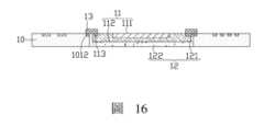
圖16為於圖15所示之塑封體表面設置導線以電連接所述第一焊墊和所述引腳後的截面示意圖。FIG16 is a cross-sectional schematic diagram after a wire is provided on the surface of the plastic package shown in FIG15 to electrically connect the first pad and the lead.
圖17為於圖16所示之導線表面設置絕緣保護層後的截面示意圖。FIG17 is a schematic cross-sectional view of the conductor shown in FIG16 after an insulating protective layer is provided on the conductor surface.
圖18為本發明另一實施例之電路連板的正面結構示意圖。Figure 18 is a schematic diagram of the front structure of a circuit board of another embodiment of the present invention.
圖19為圖18所示之電路連板的背面結構示意圖。Figure 19 is a schematic diagram of the back structure of the circuit board shown in Figure 18.
圖20為圖18所示之電路連板設於載具上的結構示意圖。FIG20 is a schematic diagram of the structure of the circuit board shown in FIG18 being arranged on a carrier.
圖21為本發明第二實施例之半導體封裝組件的截面示意圖。Figure 21 is a cross-sectional schematic diagram of the semiconductor package assembly of the second embodiment of the present invention.
圖22為本發明第二實施例之光機電模組的截面示意圖。Figure 22 is a cross-sectional schematic diagram of the optomechanical module of the second embodiment of the present invention.
圖23為本發明第二實施例之電路板的截面示意圖。Figure 23 is a cross-sectional schematic diagram of the circuit board of the second embodiment of the present invention.
圖24為將圖23所示之電路板設置於載板後的截面示意圖。FIG. 24 is a schematic cross-sectional view of the circuit board shown in FIG. 23 after being placed on a carrier board.
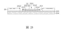
圖25為於圖24所示之收容孔內設置晶片後的截面示意圖。FIG25 is a schematic cross-sectional view of a chip after it is placed in the receiving hole shown in FIG24.
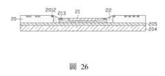
圖26為於圖25所示之收容孔內填充樹脂形成塑封體後的截面示意圖。FIG26 is a schematic cross-sectional view of the receiving hole shown in FIG25 after resin is filled to form a plastic package.
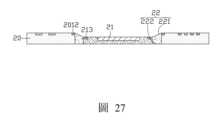
圖27為將圖26所示之載板移除後的截面示意圖。FIG27 is a schematic cross-sectional view after the carrier shown in FIG26 is removed.
圖28為於圖27所示之塑封體表面設置導線後的截面示意圖。FIG28 is a schematic cross-sectional view of the surface of the plastic package shown in FIG27 after a wire is set.
圖29為圖28所示之A部分的放大結構示意圖。Figure 29 is an enlarged structural diagram of part A shown in Figure 28.
圖30為於圖28所示之導線表面設置絕緣保護層後的截面示意圖。FIG30 is a schematic cross-sectional view of the conductor shown in FIG28 after an insulating protective layer is provided on the conductor surface.
圖31為本發明第三實施例之半導體封裝組件的截面示意圖。Figure 31 is a cross-sectional schematic diagram of the semiconductor package assembly of the third embodiment of the present invention.
圖32為本發明第四實施例之半導體封裝組件的截面示意圖。Figure 32 is a cross-sectional schematic diagram of the semiconductor package assembly of the fourth embodiment of the present invention.
下面將結合本發明實施例中的附圖,對本發明實施例中的技術方案進行清楚、完整地描述,顯然,所描述的實施例僅是本發明一部分實施例,而不是全部的實施例。基於本發明中的實施例,本領域普通技術人員在沒有做出創造性勞動前提下所獲得的所有其他實施例,都屬於本發明保護的範圍。The following will combine the attached figures in the embodiments of the present invention to clearly and completely describe the technical solutions in the embodiments of the present invention. Obviously, the described embodiments are only part of the embodiments of the present invention, not all of the embodiments. Based on the embodiments of the present invention, all other embodiments obtained by ordinary technicians in this field without creative labor are within the scope of protection of the present invention.
需要說明的是,當一個元件被認為是“連接”另一個元件,它可以是直接連接到另一個元件或者可能同時存於居中元件。當一個元件被認為是“設置於”另一個元件,它可以是直接設置於另一個元件上或者可能同時存於居中元件。It should be noted that when an element is considered to be "connected" to another element, it can be directly connected to the other element or it can exist in the center element at the same time. When an element is considered to be "set on" another element, it can be directly set on the other element or it can exist in the center element at the same time.
請參閱圖1、圖2和圖3,本發明第一實施例提供一種半導體封裝組件100,所述半導體封裝組件100包括電路板10、晶片11、塑封體12和導線13,所述電路板10包括相對的第一表面101a和第二表面101b,所述電路板10貫穿所述第一表面101a和所述第二表面101b設有至少一收容孔1011,所述電路板10的所述第一表面101a設有複數個第一焊墊1012。所述晶片11設於所述收容孔1011內且所述晶片11和所述電路板10藉由間隙114隔開,所述晶片11包括相對的有源面111和無源面112,所述有源面111和所述第一表面101a朝向同一側,所述有源面111設有複數個引腳113。所述塑封體12至少設於所述間隙114並黏接所述晶片11與所述收容孔1011的孔壁,所述導線13貼設於所述塑封體12背離所述第二表面101b的第三表面121且所述導線13電連接所述晶片11的所述引腳113和所述電路板10的所述第一焊墊1012。Please refer to Figures 1, 2 and 3. The first embodiment of the present invention provides a
在本實施例中,所述第一焊墊1012設於所述第一表面101a靠近所述晶片11的邊緣處。所述晶片11的有源面111與所述電路板10的第一表面101a以及所述塑封體12的第三表面121大致平齊。所述有源面111包括感應區1112和除所述感應區1112之外的非感應區1114,所述感應區1112位於所述有源面111的中心位置,所述非感應區1114環繞所述感應區1112設置,複數個所述引腳113設於所述非感應區1114遠離所述感應區1112的邊緣處,且所述引腳113和所述第一焊墊1012相鄰設置。In this embodiment, the
在本實施例中,所述電路板10為軟硬結合板,所述電路板10包括第一硬板部101、軟板部102和第二硬板部103。所述收容孔1011貫穿設於所述第一硬板部101,所述第二硬板部103的表面還設有電連接器1031。所述晶片11可為影像感測器、發光器或光線反射器等任意一種。In this embodiment, the
在其他實施例中,所述電路板10還可以為硬板、軟板、陶瓷基板、玻璃基板或金屬基板等任意一種。In other embodiments, the
所述半導體封裝組件100還可包括電子元件14,所述電路板10的第一表面101a上還設有第二焊墊1013,所述電子元件14藉由所述第二焊墊1013焊接於所述電路板10。The
在本實施例中,所述塑封體12還覆蓋所述晶片11的無源面112,所述塑封體12還包括與所述第三表面121相對的第四表面122,所述塑封體12的第四表面122與所述電路板10的第二表面101b大致平齊。In this embodiment, the
在一些實施例中,所述半導體封裝組件100還包括絕緣保護層132,所述絕緣保護層132覆蓋所述導線13並與所述第三表面121黏結,所述導線13位於所述絕緣保護層132與所述第三表面121之間,從而可實現所述導線13的保護和所述半導體封裝組件100表面的平整化,提高導線13的導通可靠性。In some embodiments, the
所述半導體封裝組件100中,藉由將所述晶片11設於所述電路板10的收容孔1011內並設置所述塑封體12進行保護,使得所述晶片11與所述電路板10在同一平面,可有效降低整個封裝元件的高度,且提供一個平整且高度一致的圖元平面,可有效提升成像品質。並且,相較於傳統的打金線連接,採用平面的導線13電連接所述晶片11和所述電路板10,可有效減少雜散光,提高成像品質。In the
另外,由於所述第一焊墊1012和所述引腳113相鄰設置,兩者電路短距離導通,所述電子元件14可以更靠近晶片11,電性特性更好,整個所述半導體封裝組件100的尺寸更小型化、薄型化。In addition, since the
請參閱圖4和圖5,在一些實施例中,還可在同一所述電路板10上同時開設兩個或複數個所述收容孔1011,所述收容孔1011內可分別放置相同或者不同類型的所述晶片11,藉由整合電路、提高效能,可降低成本、縮小尺寸。Please refer to Figures 4 and 5. In some embodiments, two or
在一些實施例中,所述塑封體12除覆蓋所述晶片11的無源面112之外,還可覆蓋所述電路板10的整個所述第二表面101b,從而可充當所述電路板10的補強層。In some embodiments, the
請一併參閱圖6,在一些實施例中,所述電路板10的第一表面101a上還設有密封體17,所述密封體17可包覆所述電子元件14和所述晶片11的非感應區1114,所述密封體17貫穿設有一開孔172,所述晶片11的感應區1112由所述開孔172露出。在一些實施例中,還可在所述密封體17表面設置平面的薄膜焊墊18,所述薄膜焊墊18可用於後續連接音圈馬達,或者用作散熱焊墊和/或電磁遮罩焊墊,用於匯出熱源及接地。藉由設置所述密封體17保護所述晶片11的非感應區1114,能夠擴展後續的可封裝區域,減少最終光機電模組的長寬尺寸。Please refer to FIG. 6 . In some embodiments, a sealing
請參閱圖7和圖8,在一些實施例中,所述第一焊墊1012的表面還可設有第一金屬塊1014,所述引腳113的表面可設置有第二金屬塊115,所述絕緣保護層132包覆所述第一焊墊1012、所述第一金屬塊1014、所述引腳113和所述第二金屬塊115,所述第一金屬塊1014背離所述第一焊墊1012的一端和所述第二金屬塊115背離所述引腳113的一端由所述絕緣保護層132背離所述電路板10的表面露出,所述導線13設置於所述絕緣保護層132背離所述電路板10和所述晶片11的表面,且電連接所述第一金屬塊1014從所述絕緣保護層132露出的部分和所述第二金屬塊115從所述絕緣保護層132露出的部分。Please refer to FIG. 7 and FIG. 8. In some embodiments, the surface of the
其中,所述第一金屬塊1014和所述第二金屬塊115可以為金球。藉由設置所述第一金屬塊1014和所述第二金屬塊115以及所述絕緣保護層132包覆,再設置所述導線13,可使得導線生成立體化,進一步提高導通可靠性。在具體製造過程中,在設置所述絕緣保護層132後,可條件化地加入平坦化工藝(例如研磨拋光)使得所述絕緣保護層132背離所述電路板10和所述晶片11的表面平整並露出部分所述第一金屬塊1014和部分所述第二金屬塊115。The
請參閱圖9,本發明第一實施例還提供一種應用上述半導體封裝組件100的光機電模組1000,所述光機電模組1000包括半導體封裝組件100、光學元件15、膠體152和鏡頭組件16,所述膠體152包覆所述導線13及所述絕緣保護層132,所述光學元件15藉由所述膠體152黏接於所述電路板10與所述晶片11的結合處,且所述光學元件15與所述晶片11間隔設置。所述鏡頭組件16設於所述電路板10的第一表面101a,所述鏡頭組件16與所述電路板10之間圍設形成一收容腔R,所述光學元件15和所述電子元件14收容於所述收容腔R內。Please refer to FIG. 9. The first embodiment of the present invention further provides an
在本實施例中,所述光機電模組1000為一攝像頭模組,所述光學元件15可為紅外截止濾光片,所述晶片11可為影像感測器,所述鏡頭組件16可包括音圈馬達、鏡筒和鏡頭等部件。藉由將所述光學元件15黏接在所述晶片11和所述電路板10的交界處,可有效減少整個模組長寬方向上的尺寸。In this embodiment, the
請參閱圖1至圖3、圖10至圖19,本發明第一實施例還提供一種半導體封裝組件100的製造方法,包括以下步驟:Please refer to Figures 1 to 3 and Figures 10 to 19. The first embodiment of the present invention also provides a method for manufacturing a
步驟S11:請參閱圖10,提供一電路板10,所述電路板10貫穿設有至少一收容孔1011,所述電路板10其中一表面設有複數個第一焊墊1012。Step S11: Please refer to Figure 10, provide a
請參閱圖11,在本實施例中,所述電路板10為軟硬結合板,所述電路板10包括第一硬板部101、軟板部102和第二硬板部103。所述第一硬板部101包括相對設置的第一表面101a和第二表面101b,所述收容孔1011貫穿所述第一表面101a和所述第二表面101b,所述第一焊墊1012設於所述第一表面101a。所述第二硬板部103的表面還設有電連接器1031。Please refer to Figure 11. In this embodiment, the
在其他實施例中,所述電路板10還可以為硬板、軟板、陶瓷基板、玻璃基板或金屬基板等任意一種。In other embodiments, the
在一些實施例中,所述第一表面101a上還設有與所述第一焊墊1012間隔設置的第二焊墊1013。In some embodiments, a
步驟S12:請參閱圖12和圖13,於所述電路板10的第一表面101a疊設一載板104,所述載板104朝向所述電路板10的表面設有可剝離膜105,於所述收容孔1011內放置一晶片11。Step S12: Please refer to Figures 12 and 13. A
所述晶片11包括相對的有源面111和無源面112,所述有源面111朝向所述可剝離膜105設置。所述有源面111包括感應區1112和除所述感應區1112之外的非感應區1114,所述非感應區1114內設有複數個間隔設置的引腳113。在本實施例中,所述感應區1112位於所述有源面111的中心位置,所述非感應區1114環繞所述感應區1112設置,複數個所述引腳113設於所述非感應區1114遠離所述感應區1112的邊緣處,複數個所述引腳113和所述第一焊墊1012相鄰設置。在本實施例中,所述晶片11為測試完成的良好晶片(Known Good Die,KGD),可藉由從單一或多種晶圓上拿取校準對位擺放在所述收容孔1011內。The
其中,所述收容孔1011的尺寸大於所述晶片11的尺寸,從而所述晶片11與所述電路板10之間形成一間隙114。在本實施例中,所述第一焊墊1012設於所述第一表面101a靠近所述晶片11的邊緣處,從而所述第一焊墊1012和所述引腳113相鄰設置。The size of the receiving
步驟S13:請參閱圖14和圖15,至少於所述間隙114內填充樹脂形成塑封體12,並移除所述可剝離膜105和所述載板104。Step S13: Please refer to Figures 14 and 15, fill the
具體地,可採用注塑成型工藝(molding)工藝於所述間隙114內形成所述塑封體12。Specifically, the
其中,部分填充入所述間隙114以黏接所述晶片11與所述收容孔1011的孔壁,另一部分所述塑封體12覆蓋所述晶片11的無源面112,使得所述晶片11可牢固固定於所述收容孔1011內,強化整體模組的結構強度。Part of the
所述塑封體12包括背離所述第二表面101b的第三表面121,以及與所述第三表面121相對的第四表面122,所述第三表面與所述晶片11的有源面111和所述電路板10的第一表面101a大致平齊。所述第四表面122與所述電路板10的第二表面101b大致平齊。The
步驟S14:請參閱圖16,於所述塑封體12的第三表面121貼設導線13以電連接所述晶片11的引腳113和所述電路板10的第一焊墊1012。Step S14: Please refer to Figure 16, a
具體地,可藉由噴塗導電材料的方式於所述第三表面121形成平整的導通薄膜線路,即所述導線13。Specifically, a flat conductive film circuit, namely the
請參閱圖17,在一些實施例中,步驟S14還包括:於所述導線13表面覆蓋絕緣保護層132,以提高導通可靠性。Please refer to Figure 17. In some embodiments, step S14 further includes: covering the surface of the
在一些實施例中,請參閱圖18、圖19和圖20,可採用電路板連板製程,同時對複數個電路板進行製造,可以控制雙模組或更多模組成像/發射面在同一平面,獲得更佳品質的光學模組。具體地,電路連板L包括複數個電路板單板,可在每一所述電路板單板上收容孔後,將電路連板L置於一載具Z表面,所述載具Z表面設有弱黏性的可剝離膜105a,在所述電路連板L的單個所述電路板10上分別製造,最後切割分單即可。In some embodiments, please refer to Figures 18, 19 and 20. A circuit board connecting process can be used to manufacture multiple circuit boards at the same time, and the imaging/emitting surfaces of dual modules or more modules can be controlled to be on the same plane, so as to obtain an optical module with better quality. Specifically, the circuit board L includes multiple circuit board single boards. After the receiving holes are provided on each of the circuit board single boards, the circuit board L can be placed on the surface of a carrier Z. The surface of the carrier Z is provided with a weakly sticky
步驟S15:請參閱圖1,於所述第一表面101a設置電子元件14,獲得所述半導體封裝組件100。Step S15: Please refer to Figure 1, set the
具體地,可藉由表面貼裝技術(SMT)將所述電子元件14焊接於所述第二焊墊1013。其中,所述電子元件14的數量可為複數個,複數個所述電子元件14可為主動元件和/或被動元件。Specifically, the
請參閱圖21,本發明第二實施例提供一種半導體封裝組件200,所述半導體封裝組件200與所述半導體封裝組件100的結構大致相同,不同之處在於:Please refer to Figure 21. The second embodiment of the present invention provides a
所述晶片21的有源面211的高度低於所述電路板20的第一表面201a的高度,即所述有源面211位於所述第一表面201a和第二表面201b之間。所述塑封體22僅填充於所述晶片21與所述電路板20之間的間隙214,所述塑封體22的第三表面221為一傾斜面連接所述第一表面201a和第二表面201b,所述晶片21的無源面212與所述電路板20的第二表面201b以及所述塑封體22的第四表面222大致平齊。The height of the
請參閱圖22,本發明第二實施例還提供一種應用上述半導體封裝組件200的光機電模組2000,所述光機電模組2000與所述光機電模組1000的結構大致相同,在此不再贅述。Please refer to FIG. 22 . The second embodiment of the present invention also provides an
請參閱圖21、圖23至圖30,本發明第二實施例還提供一種半導體封裝組件200的製造方法,包括以下步驟:Please refer to Figures 21, 23 to 30. The second embodiment of the present invention also provides a method for manufacturing a
步驟S21:請參閱圖22,提供一電路板20,所述電路板20貫穿設有至少一收容孔2011,所述電路板20包括相對的第一表面201a和第二表面201b,所述第一表面201a上間隔設有複數個第一焊墊2012。Step S21: Please refer to Figure 22, provide a
在一些實施例中,所述第一表面201a上還設有與所述第一焊墊2012間隔設置的第二焊墊2013。In some embodiments, a
步驟S22:請參閱圖23和圖24,於所述電路板20的第二表面201b的一側疊設一可剝離膜205和載板204,並於所述收容孔1011內放置一晶片21。Step S22: Please refer to Figures 23 and 24, a
所述晶片21包括相對的有源面211和無源面212,所述無源面212朝向所述可剝離膜205設置。所述有源面111包括感應區2112和除所述感應區2112之外的非感應區2114,所述非感應區2114內設有複數個間隔設置的引腳213。在本實施例中,所述感應區1112位於所述有源面111的中心位置,所述非感應區2114環繞所述感應區2112設置,複數個所述引腳213設於所述非感應區1114遠離所述感應區2112的一邊緣處。其中,所述第一焊墊2012設於所述第一表面201a靠近所述晶片21的邊緣處,複數個所述引腳213和所述第一焊墊2012相鄰設置。The
所述收容孔2011的尺寸大於所述晶片21的尺寸,從而所述晶片21與所述電路板20之間形成一間隙214。在本實施例中,所述晶片21的有源面211的高度低於所述電路板20的第一表面201a的高度,即所述有源面211位於所述第一表面201a和第二表面201b之間。The size of the receiving
步驟S23:請參閱圖25和圖26,於所述間隙214內填充樹脂形成塑封體22,並移除所述可剝離膜205和所述載板204,所述塑封體22黏接所述晶片21和所述收容孔2011的孔壁。Step S23: Please refer to Figures 25 and 26, fill the
步驟S24:請參閱圖27和圖28,於所述塑封體22的第三表面221貼設導線23以電連接所述晶片21的引腳213和所述電路板20的第一焊墊2012。Step S24: Please refer to Figures 27 and 28, a
請參閱圖29,在一些實施例中,步驟S24還包括:於所述導線23的表面設置絕緣保護層232,以提高導通可靠性。Please refer to Figure 29. In some embodiments, step S24 further includes: providing an insulating
步驟S25:請參閱圖21,於所述第一表面201a設置電子元件24,獲得半導體封裝組件200。Step S25: Please refer to Figure 21, set the
具體地,可藉由表面貼裝技術(SMT)將所述電子元件24焊接於所述第二焊墊2013。其中,所述電子元件24的數量可為複數個,複數個所述電子元件24可為主動元件和/或被動元件。Specifically, the
請參閱圖31,本發明第三實施例還提供一種半導體封裝組件300,所述半導體封裝組件300與所述半導體封裝組件100的結構大致相同,不同之處在於:Please refer to Figure 31. The third embodiment of the present invention also provides a
所述電路板30的第一表面301a朝第二表面301b內凹設有收容孔3011,所述晶片31設於所述收容孔3011內,所述晶片31的無源面312貼設於所述收容孔3011的底壁。所述塑封體32僅填充於所述晶片31與所述電路板30之間的間隙314內。The
其中,所述晶片31的無源面312之間可設有黏結層(圖未示),例如可藉由設置DAF膜(Die Attach Film)將所述晶片31黏結於所述電路板30。Among them, a bonding layer (not shown) may be provided between the
請參閱圖32,本發明第四實施例還提供一種無基板封裝的半導體封裝組件400,所述半導體封裝組件400與所述半導體封裝組件100的區別在於,所述半導體封裝組件400不包括電路板10,所述塑封體42包覆所述晶片41的無源面412和側面。Please refer to FIG. 32 . The fourth embodiment of the present invention also provides a
所述塑封體42包括相對的第三表面42a和第四表面42b,所述晶片41的有源面411和所述第三表面42a大致平齊。所述第三表面42a朝第四表面42b內凹設有收容孔421,所述晶片41設於所述收容孔421內。所述第三表面42a靠近所述晶片41的邊緣處間隔設有複數個第一焊墊422和第二焊墊423,所述晶片41的引腳413和所述第一焊墊422藉由導線43電連接,所述電子元件44藉由所述第二焊墊423焊接於所述第三表面42a。The
具體地,可採用重新佈線技術(Redistribution Layer,RDL)首先將所述晶片41倒置於一載板上(即有源面411朝向載板),然後於所述晶片41填充樹脂形成所述塑封體42,去除所述載板後。在所述塑封體42上重新佈線形成所述第一焊墊422和第二焊墊423,後續設置所述導線43和所述電子元件4即可。Specifically, the
以上所述,僅是本發明的較佳實施方式而已,並非對本發明任何形式上的限制,雖然本發明已是較佳實施方式揭露如上,並非用以限定本發明,任何熟悉本專業的技術人員,在不脫離本發明技術方案範圍內,當可利用上述揭示的技術內容做出些許更動或修飾為等同變化的等效實施方式,但凡是未脫離本發明技術方案內容,依據本發明的技術實質對以上實施方式所做的任何簡單修改、等同變化與修飾,均仍屬於本發明技術方案的範圍內。The above is only the preferred implementation of the present invention, and does not constitute any form of limitation on the present invention. Although the present invention has been disclosed as the preferred implementation, it is not intended to limit the present invention. Any technician familiar with this profession can make some changes or modifications to the above disclosed technical contents within the scope of the technical solution of the present invention. However, any simple modification, equivalent change and modification made to the above implementation according to the technical essence of the present invention without departing from the content of the technical solution of the present invention still falls within the scope of the technical solution of the present invention.
100:半導體封裝組件100:Semiconductor packaging components
10:電路板10: Circuit board
101a:第一表面101a: first surface
101b:第二表面101b: Second surface
1011:收容孔1011: Receiving hole
1012:第一焊墊1012: First welding pad
1013:第二焊墊1013: Second welding pad
11:晶片11: Chip
111:有源面111: Active surface
1112:感應區1112: Sensing area
1114:非感應區1114: Non-sensitive area
112:無源面112: Passive surface
113:引腳113: Pins
114:間隙114: Gap
12:塑封體12: Plastic sealing body
121:第三表面121: Third surface
122:第四表面122: The fourth surface
13:導線13: Wire
132:絕緣保護層132: Insulation protective layer
14:電子元件14: Electronic components
Claims (11)
Translated fromChinesePriority Applications (1)
| Application Number | Priority Date | Filing Date | Title |
|---|---|---|---|
| TW112125581ATWI866326B (en) | 2023-07-07 | 2023-07-07 | Manufacturing method of semiconductor packaging assembly and semiconductor packaging assembly and optoelectromechanical module |
Applications Claiming Priority (1)
| Application Number | Priority Date | Filing Date | Title |
|---|---|---|---|
| TW112125581ATWI866326B (en) | 2023-07-07 | 2023-07-07 | Manufacturing method of semiconductor packaging assembly and semiconductor packaging assembly and optoelectromechanical module |
Publications (2)
| Publication Number | Publication Date |
|---|---|
| TWI866326Btrue TWI866326B (en) | 2024-12-11 |
| TW202503912A TW202503912A (en) | 2025-01-16 |
Family
ID=94769305
Family Applications (1)
| Application Number | Title | Priority Date | Filing Date |
|---|---|---|---|
| TW112125581ATWI866326B (en) | 2023-07-07 | 2023-07-07 | Manufacturing method of semiconductor packaging assembly and semiconductor packaging assembly and optoelectromechanical module |
Country Status (1)
| Country | Link |
|---|---|
| TW (1) | TWI866326B (en) |
Citations (2)
| Publication number | Priority date | Publication date | Assignee | Title |
|---|---|---|---|---|
| US20140339668A1 (en)* | 2012-02-07 | 2014-11-20 | Nikon Corporation | Imaging unit and imaging apparatus |
| US20220045112A1 (en)* | 2018-11-20 | 2022-02-10 | Ningbo Semiconductor International Corporation | Camera assembly, lens module, and electronic device |
- 2023
- 2023-07-07TWTW112125581Apatent/TWI866326B/enactive
Patent Citations (2)
| Publication number | Priority date | Publication date | Assignee | Title |
|---|---|---|---|---|
| US20140339668A1 (en)* | 2012-02-07 | 2014-11-20 | Nikon Corporation | Imaging unit and imaging apparatus |
| US20220045112A1 (en)* | 2018-11-20 | 2022-02-10 | Ningbo Semiconductor International Corporation | Camera assembly, lens module, and electronic device |
Also Published As
| Publication number | Publication date |
|---|---|
| TW202503912A (en) | 2025-01-16 |
Similar Documents
| Publication | Publication Date | Title |
|---|---|---|
| KR100493063B1 (en) | BGA package with stacked semiconductor chips and manufacturing method thereof | |
| CN1104745C (en) | Solid-state imaging device and manufacturing method thereof | |
| US7763964B2 (en) | Semiconductor device and semiconductor module using the same | |
| KR100652375B1 (en) | Image sensor module structure including wire bonding package and manufacturing method thereof | |
| US7282693B2 (en) | Camera module for compact electronic equipments | |
| US5418566A (en) | Compact imaging apparatus for electronic endoscope with improved optical characteristics | |
| CN100416816C (en) | Method for manufacturing solid-state imaging device | |
| US9508687B2 (en) | Low cost hybrid high density package | |
| US7138695B2 (en) | Image sensor module and method for fabricating the same | |
| US7511367B2 (en) | Optical device and method for fabricating the same | |
| US20040089921A1 (en) | Lead frame and method of producing the same, and resin-encapsulated semiconductor device and method of producing the same | |
| CN100490162C (en) | Solid-state imaging device and method for producing the same | |
| US8077248B2 (en) | Optical device and production method thereof | |
| US20060016973A1 (en) | Multi-chip image sensor package module | |
| JP2008092417A (en) | Semiconductor imaging device, method for manufacturing the same, semiconductor imaging device, and semiconductor imaging module | |
| US20110180891A1 (en) | Conductor package structure and method of the same | |
| KR20030018642A (en) | Stack chip module | |
| CN101271913A (en) | Optical devices, camera modules, mobile phones, digital still cameras, and medical endoscopes | |
| US11804464B2 (en) | Semiconductor device and manufacturing method thereof | |
| US20220093673A1 (en) | Image sensor packages | |
| US20110083322A1 (en) | Optical device and method for manufacturing the same | |
| US20070278639A1 (en) | Semiconductor Device Stack and Method for Its Production | |
| US7242538B2 (en) | Optical device | |
| TWI866326B (en) | Manufacturing method of semiconductor packaging assembly and semiconductor packaging assembly and optoelectromechanical module | |
| CN117038683B (en) | Opto-mechanical-electrical module, semiconductor packaging assembly and manufacturing method thereof |