TWI863785B - Method of fabricating semiconductor device, multi-gate semiconductor device and method of fabricating the same - Google Patents
Method of fabricating semiconductor device, multi-gate semiconductor device and method of fabricating the sameDownload PDFInfo
- Publication number
- TWI863785B TWI863785BTW112151435ATW112151435ATWI863785BTW I863785 BTWI863785 BTW I863785BTW 112151435 ATW112151435 ATW 112151435ATW 112151435 ATW112151435 ATW 112151435ATW I863785 BTWI863785 BTW I863785B
- Authority
- TW
- Taiwan
- Prior art keywords
- layer
- gate
- fin
- doping
- epitaxial
- Prior art date
Links
Images


Classifications
- H—ELECTRICITY
- H10—SEMICONDUCTOR DEVICES; ELECTRIC SOLID-STATE DEVICES NOT OTHERWISE PROVIDED FOR
- H10D—INORGANIC ELECTRIC SEMICONDUCTOR DEVICES
- H10D30/00—Field-effect transistors [FET]
- H10D30/01—Manufacture or treatment
- H10D30/021—Manufacture or treatment of FETs having insulated gates [IGFET]
- H10D30/024—Manufacture or treatment of FETs having insulated gates [IGFET] of fin field-effect transistors [FinFET]
- H—ELECTRICITY
- H10—SEMICONDUCTOR DEVICES; ELECTRIC SOLID-STATE DEVICES NOT OTHERWISE PROVIDED FOR
- H10D—INORGANIC ELECTRIC SEMICONDUCTOR DEVICES
- H10D30/00—Field-effect transistors [FET]
- H10D30/501—FETs having stacked nanowire, nanosheet or nanoribbon channels
- H10D30/502—FETs having stacked nanowire, nanosheet or nanoribbon channels characterised by the stacked channels
- H10D30/503—FETs having stacked nanowire, nanosheet or nanoribbon channels characterised by the stacked channels having non-rectangular cross-sections
- H—ELECTRICITY
- H10—SEMICONDUCTOR DEVICES; ELECTRIC SOLID-STATE DEVICES NOT OTHERWISE PROVIDED FOR
- H10D—INORGANIC ELECTRIC SEMICONDUCTOR DEVICES
- H10D30/00—Field-effect transistors [FET]
- H10D30/01—Manufacture or treatment
- H10D30/014—Manufacture or treatment of FETs having zero-dimensional [0D] or one-dimensional [1D] channels, e.g. quantum wire FETs, single-electron transistors [SET] or Coulomb blockade transistors
- H—ELECTRICITY
- H10—SEMICONDUCTOR DEVICES; ELECTRIC SOLID-STATE DEVICES NOT OTHERWISE PROVIDED FOR
- H10D—INORGANIC ELECTRIC SEMICONDUCTOR DEVICES
- H10D30/00—Field-effect transistors [FET]
- H10D30/01—Manufacture or treatment
- H10D30/019—Manufacture or treatment of FETs having stacked nanowire, nanosheet or nanoribbon channels
- H10D30/0191—Manufacture or treatment of FETs having stacked nanowire, nanosheet or nanoribbon channels forming stacked channels, e.g. changing their shapes or sizes
- H10D30/0193—Manufacture or treatment of FETs having stacked nanowire, nanosheet or nanoribbon channels forming stacked channels, e.g. changing their shapes or sizes by modifying properties of the stacked channels
- H—ELECTRICITY
- H10—SEMICONDUCTOR DEVICES; ELECTRIC SOLID-STATE DEVICES NOT OTHERWISE PROVIDED FOR
- H10D—INORGANIC ELECTRIC SEMICONDUCTOR DEVICES
- H10D30/00—Field-effect transistors [FET]
- H10D30/40—FETs having zero-dimensional [0D], one-dimensional [1D] or two-dimensional [2D] charge carrier gas channels
- H10D30/43—FETs having zero-dimensional [0D], one-dimensional [1D] or two-dimensional [2D] charge carrier gas channels having 1D charge carrier gas channels, e.g. quantum wire FETs or transistors having 1D quantum-confined channels
- H—ELECTRICITY
- H10—SEMICONDUCTOR DEVICES; ELECTRIC SOLID-STATE DEVICES NOT OTHERWISE PROVIDED FOR
- H10D—INORGANIC ELECTRIC SEMICONDUCTOR DEVICES
- H10D30/00—Field-effect transistors [FET]
- H10D30/60—Insulated-gate field-effect transistors [IGFET]
- H10D30/62—Fin field-effect transistors [FinFET]
- H10D30/6211—Fin field-effect transistors [FinFET] having fin-shaped semiconductor bodies integral with the bulk semiconductor substrates
- H—ELECTRICITY
- H10—SEMICONDUCTOR DEVICES; ELECTRIC SOLID-STATE DEVICES NOT OTHERWISE PROVIDED FOR
- H10D—INORGANIC ELECTRIC SEMICONDUCTOR DEVICES
- H10D62/00—Semiconductor bodies, or regions thereof, of devices having potential barriers
- H10D62/10—Shapes, relative sizes or dispositions of the regions of the semiconductor bodies; Shapes of the semiconductor bodies
- H10D62/117—Shapes of semiconductor bodies
- H10D62/118—Nanostructure semiconductor bodies
- H10D62/119—Nanowire, nanosheet or nanotube semiconductor bodies
- H10D62/121—Nanowire, nanosheet or nanotube semiconductor bodies oriented parallel to substrates
- H—ELECTRICITY
- H10—SEMICONDUCTOR DEVICES; ELECTRIC SOLID-STATE DEVICES NOT OTHERWISE PROVIDED FOR
- H10D—INORGANIC ELECTRIC SEMICONDUCTOR DEVICES
- H10D62/00—Semiconductor bodies, or regions thereof, of devices having potential barriers
- H10D62/10—Shapes, relative sizes or dispositions of the regions of the semiconductor bodies; Shapes of the semiconductor bodies
- H10D62/13—Semiconductor regions connected to electrodes carrying current to be rectified, amplified or switched, e.g. source or drain regions
- H10D62/149—Source or drain regions of field-effect devices
- H10D62/151—Source or drain regions of field-effect devices of IGFETs
- H—ELECTRICITY
- H10—SEMICONDUCTOR DEVICES; ELECTRIC SOLID-STATE DEVICES NOT OTHERWISE PROVIDED FOR
- H10D—INORGANIC ELECTRIC SEMICONDUCTOR DEVICES
- H10D64/00—Electrodes of devices having potential barriers
- H10D64/01—Manufacture or treatment
- H10D64/017—Manufacture or treatment using dummy gates in processes wherein at least parts of the final gates are self-aligned to the dummy gates, i.e. replacement gate processes
- H—ELECTRICITY
- H10—SEMICONDUCTOR DEVICES; ELECTRIC SOLID-STATE DEVICES NOT OTHERWISE PROVIDED FOR
- H10D—INORGANIC ELECTRIC SEMICONDUCTOR DEVICES
- H10D64/00—Electrodes of devices having potential barriers
- H10D64/20—Electrodes characterised by their shapes, relative sizes or dispositions
- H10D64/27—Electrodes not carrying the current to be rectified, amplified, oscillated or switched, e.g. gates
- H10D64/311—Gate electrodes for field-effect devices
- H10D64/411—Gate electrodes for field-effect devices for FETs
- H10D64/511—Gate electrodes for field-effect devices for FETs for IGFETs
- H10D64/514—Gate electrodes for field-effect devices for FETs for IGFETs characterised by the insulating layers
- H—ELECTRICITY
- H10—SEMICONDUCTOR DEVICES; ELECTRIC SOLID-STATE DEVICES NOT OTHERWISE PROVIDED FOR
- H10D—INORGANIC ELECTRIC SEMICONDUCTOR DEVICES
- H10D84/00—Integrated devices formed in or on semiconductor substrates that comprise only semiconducting layers, e.g. on Si wafers or on GaAs-on-Si wafers
- H10D84/01—Manufacture or treatment
- H10D84/0123—Integrating together multiple components covered by H10D12/00 or H10D30/00, e.g. integrating multiple IGBTs
- H10D84/0126—Integrating together multiple components covered by H10D12/00 or H10D30/00, e.g. integrating multiple IGBTs the components including insulated gates, e.g. IGFETs
- H10D84/0165—Integrating together multiple components covered by H10D12/00 or H10D30/00, e.g. integrating multiple IGBTs the components including insulated gates, e.g. IGFETs the components including complementary IGFETs, e.g. CMOS devices
- H10D84/0167—Manufacturing their channels
- H—ELECTRICITY
- H10—SEMICONDUCTOR DEVICES; ELECTRIC SOLID-STATE DEVICES NOT OTHERWISE PROVIDED FOR
- H10D—INORGANIC ELECTRIC SEMICONDUCTOR DEVICES
- H10D84/00—Integrated devices formed in or on semiconductor substrates that comprise only semiconducting layers, e.g. on Si wafers or on GaAs-on-Si wafers
- H10D84/01—Manufacture or treatment
- H10D84/0123—Integrating together multiple components covered by H10D12/00 or H10D30/00, e.g. integrating multiple IGBTs
- H10D84/0126—Integrating together multiple components covered by H10D12/00 or H10D30/00, e.g. integrating multiple IGBTs the components including insulated gates, e.g. IGFETs
- H10D84/0165—Integrating together multiple components covered by H10D12/00 or H10D30/00, e.g. integrating multiple IGBTs the components including insulated gates, e.g. IGFETs the components including complementary IGFETs, e.g. CMOS devices
- H10D84/0193—Integrating together multiple components covered by H10D12/00 or H10D30/00, e.g. integrating multiple IGBTs the components including insulated gates, e.g. IGFETs the components including complementary IGFETs, e.g. CMOS devices the components including FinFETs
- H—ELECTRICITY
- H10—SEMICONDUCTOR DEVICES; ELECTRIC SOLID-STATE DEVICES NOT OTHERWISE PROVIDED FOR
- H10D—INORGANIC ELECTRIC SEMICONDUCTOR DEVICES
- H10D84/00—Integrated devices formed in or on semiconductor substrates that comprise only semiconducting layers, e.g. on Si wafers or on GaAs-on-Si wafers
- H10D84/01—Manufacture or treatment
- H10D84/02—Manufacture or treatment characterised by using material-based technologies
- H10D84/03—Manufacture or treatment characterised by using material-based technologies using Group IV technology, e.g. silicon technology or silicon-carbide [SiC] technology
- H10D84/038—Manufacture or treatment characterised by using material-based technologies using Group IV technology, e.g. silicon technology or silicon-carbide [SiC] technology using silicon technology, e.g. SiGe
- H—ELECTRICITY
- H10—SEMICONDUCTOR DEVICES; ELECTRIC SOLID-STATE DEVICES NOT OTHERWISE PROVIDED FOR
- H10D—INORGANIC ELECTRIC SEMICONDUCTOR DEVICES
- H10D84/00—Integrated devices formed in or on semiconductor substrates that comprise only semiconducting layers, e.g. on Si wafers or on GaAs-on-Si wafers
- H10D84/80—Integrated devices formed in or on semiconductor substrates that comprise only semiconducting layers, e.g. on Si wafers or on GaAs-on-Si wafers characterised by the integration of at least one component covered by groups H10D12/00 or H10D30/00, e.g. integration of IGFETs
- H10D84/82—Integrated devices formed in or on semiconductor substrates that comprise only semiconducting layers, e.g. on Si wafers or on GaAs-on-Si wafers characterised by the integration of at least one component covered by groups H10D12/00 or H10D30/00, e.g. integration of IGFETs of only field-effect components
- H10D84/83—Integrated devices formed in or on semiconductor substrates that comprise only semiconducting layers, e.g. on Si wafers or on GaAs-on-Si wafers characterised by the integration of at least one component covered by groups H10D12/00 or H10D30/00, e.g. integration of IGFETs of only field-effect components of only insulated-gate FETs [IGFET]
- H10D84/85—Complementary IGFETs, e.g. CMOS
- H10D84/853—Complementary IGFETs, e.g. CMOS comprising FinFETs
- B—PERFORMING OPERATIONS; TRANSPORTING
- B82—NANOTECHNOLOGY
- B82Y—SPECIFIC USES OR APPLICATIONS OF NANOSTRUCTURES; MEASUREMENT OR ANALYSIS OF NANOSTRUCTURES; MANUFACTURE OR TREATMENT OF NANOSTRUCTURES
- B82Y10/00—Nanotechnology for information processing, storage or transmission, e.g. quantum computing or single electron logic
- H—ELECTRICITY
- H10—SEMICONDUCTOR DEVICES; ELECTRIC SOLID-STATE DEVICES NOT OTHERWISE PROVIDED FOR
- H10D—INORGANIC ELECTRIC SEMICONDUCTOR DEVICES
- H10D30/00—Field-effect transistors [FET]
- H10D30/60—Insulated-gate field-effect transistors [IGFET]
- H10D30/67—Thin-film transistors [TFT]
- H10D30/6729—Thin-film transistors [TFT] characterised by the electrodes
- H10D30/673—Thin-film transistors [TFT] characterised by the electrodes characterised by the shapes, relative sizes or dispositions of the gate electrodes
- H10D30/6735—Thin-film transistors [TFT] characterised by the electrodes characterised by the shapes, relative sizes or dispositions of the gate electrodes having gates fully surrounding the channels, e.g. gate-all-around
- H—ELECTRICITY
- H10—SEMICONDUCTOR DEVICES; ELECTRIC SOLID-STATE DEVICES NOT OTHERWISE PROVIDED FOR
- H10D—INORGANIC ELECTRIC SEMICONDUCTOR DEVICES
- H10D30/00—Field-effect transistors [FET]
- H10D30/60—Insulated-gate field-effect transistors [IGFET]
- H10D30/67—Thin-film transistors [TFT]
- H10D30/6757—Thin-film transistors [TFT] characterised by the structure of the channel, e.g. transverse or longitudinal shape or doping profile
- H—ELECTRICITY
- H10—SEMICONDUCTOR DEVICES; ELECTRIC SOLID-STATE DEVICES NOT OTHERWISE PROVIDED FOR
- H10D—INORGANIC ELECTRIC SEMICONDUCTOR DEVICES
- H10D30/00—Field-effect transistors [FET]
- H10D30/60—Insulated-gate field-effect transistors [IGFET]
- H10D30/791—Arrangements for exerting mechanical stress on the crystal lattice of the channel regions
- H10D30/797—Arrangements for exerting mechanical stress on the crystal lattice of the channel regions being in source or drain regions, e.g. SiGe source or drain
Landscapes
- Insulated Gate Type Field-Effect Transistor (AREA)
Abstract
Description
Translated fromChinese本揭示內容是關於製造半導體裝置的方法、多閘極半導體裝置及其製造方法。This disclosure relates to a method for manufacturing a semiconductor device, a multi-gate semiconductor device and a method for manufacturing the same.
電子產業對於更小、更快且同時具有支援更多日益複雜和精密功能的電子裝置的需求不斷增加。因此半導體產業製造成本低、性能高且功耗低的積體電路(IC)的趨勢持續存在。到目前為止,這些目標在很大程度上是藉由縮小半導體IC的尺寸(例如最小特徵尺寸)來實現的,從而提高生產效率並降低相關成本。然而這種尺寸的縮小也增加了半導體製造製程的複雜性。因此半導體IC和裝置的持續進步需要相關的半導體製造製程和技術的進步。The electronics industry has an increasing demand for smaller, faster electronic devices that support more increasingly complex and sophisticated functions. Therefore, the semiconductor industry continues to manufacture low-cost, high-performance, and low-power integrated circuits (ICs). To date, these goals have been achieved in large part by reducing the size of semiconductor ICs (e.g., minimum feature size), thereby increasing production efficiency and reducing associated costs. However, this reduction in size has also increased the complexity of semiconductor manufacturing processes. Therefore, continued advancement of semiconductor ICs and devices requires advancement of related semiconductor manufacturing processes and technologies.
僅作為一個例子,製造具有低密度的介面阱(interface trap)和氧化物阱(oxide trap)的電晶體對於提供高性能的裝置至關重要。然而隨著IC尺寸的不斷縮小和多閘極裝置(例如鰭式場效電晶體(fin field-effect transistor,FinFET))的引入,隨之的挑戰也增加。其中一個挑戰是雜訊,例如閃爍(1/f)雜訊,其可由介面阱和氧化物阱引起,並且降低裝置性能。此外,鑒於多閘極裝置的電晶體的通道至閘極介電介面(channel-to-gate dielectric interface)的表面積比例增加,在通道至閘極介電介面處的載流子的電荷被捕捉(trapped)機率可能增加。As just one example, fabricating transistors with low density of interface traps and oxide traps is critical to providing high performance devices. However, with the continued scaling of ICs and the introduction of multi-gate devices such as fin field-effect transistors (FinFETs), challenges are increasing. One such challenge is noise, such as flicker (1/f) noise, which can be caused by interface traps and oxide traps and degrade device performance. In addition, given the increased surface area ratio of the channel-to-gate dielectric interface of the transistor in a multi-gate device, the probability of carriers being trapped at the channel-to-gate dielectric interface may increase.
因此,現有技術在所有方面並非完全令人滿意。Therefore, the prior art is not completely satisfactory in all aspects.
本揭示內容提供一種製造半導體裝置的方法。方法包括以下操作。提供從基板延伸的第一鰭。形成第一閘極堆疊在第一鰭上。形成第一摻雜層沿著第一鰭的表面及第一閘極堆疊下方,其中第一摻雜層的第一摻雜劑種類與半導體裝置的源極/汲極特徵的第二摻雜劑種類具有相同的極性。The present disclosure provides a method for manufacturing a semiconductor device. The method includes the following operations. Providing a first fin extending from a substrate. Forming a first gate stack on the first fin. Forming a first doping layer along a surface of the first fin and below the first gate stack, wherein a first dopant type of the first doping layer has the same polarity as a second dopant type of a source/drain feature of the semiconductor device.
本揭示內容也提供一種製造多閘極半導體裝置的方法。方法包括以下操作。提供從基板延伸的鰭,其中鰭包括具有複數個第二磊晶層插置其間的複數個第一磊晶層。選擇性地移除第二磊晶層以在這些第一磊晶層中相鄰的多者之間形成多個間隙並暴露出第一磊晶層的多個表面。在第一磊晶層暴露的表面上形成第一摻雜層。執行趨入退火以使得第一摻雜層中的多個摻雜劑擴散到第一磊晶層的表面,以沿著第一磊晶層的表面形成第二摻雜層。在執行趨入退火之後,移除第一摻雜層的剩餘部分。The present disclosure also provides a method for manufacturing a multi-gate semiconductor device. The method includes the following operations. A fin extending from a substrate is provided, wherein the fin includes a plurality of first epitaxial layers having a plurality of second epitaxial layers interposed therebetween. The second epitaxial layers are selectively removed to form a plurality of gaps between adjacent ones of the first epitaxial layers and to expose a plurality of surfaces of the first epitaxial layers. A first doping layer is formed on the exposed surface of the first epitaxial layer. A run-in anneal is performed to diffuse a plurality of dopants in the first doping layer to the surface of the first epitaxial layer to form a second doping layer along the surface of the first epitaxial layer. After the run-in anneal is performed, the remaining portion of the first doping layer is removed.
本揭示內容還提供一種多閘極半導體裝置。多閘極半導體裝置包括包括複數個矽磊晶層的第一鰭、在第一鰭的通道區域上的第一閘極結構,以及與第一鰭的通道區域相鄰的第一磊晶源極/汲極特徵。矽磊晶層中的每一個包括沿著矽磊晶層的表面的第一摻雜層,以及第一摻雜層具有第一極性類型及第一摻雜劑濃度。第一閘極結構的一部分設置在矽磊晶層的相鄰多層之間。第一磊晶源極/汲極特徵具有與第一極性類型相同的第二極性類型,以及第一磊晶源極/汲極特徵具有大於第一摻雜劑濃度的第二摻雜劑濃度。The present disclosure also provides a multi-gate semiconductor device. The multi-gate semiconductor device includes a first fin including a plurality of silicon epitaxial layers, a first gate structure on a channel region of the first fin, and a first epitaxial source/drain feature adjacent to the channel region of the first fin. Each of the silicon epitaxial layers includes a first doped layer along a surface of the silicon epitaxial layer, and the first doped layer has a first polarity type and a first dopant concentration. A portion of the first gate structure is disposed between adjacent layers of the silicon epitaxial layer. The first epitaxial source/drain features have a second polarity type that is the same as the first polarity type, and the first epitaxial source/drain features have a second dopant concentration that is greater than the first dopant concentration.
100:電晶體100: Transistor
102:基板102: Substrate
104:閘極堆疊104: Gate stack
106:閘極介電質106: Gate dielectric
108:閘極電極108: Gate electrode
110:源極區域110: Source region
112:汲極區域112: Drain area
114:通道區域114: Channel area
150:多閘極裝置150:Multi-gate device
152:基板152: Substrate
154:鰭154: Fins
155:源極區域155: Source region
156:隔離區域156: Isolation area
157:汲極區域157: Drain area
158:閘極結構158: Gate structure
160:介面層160: Interface layer
162:閘極介電層162: Gate dielectric layer
164:金屬層164:Metal layer
200:方法200:Methods
202:方塊202: Block
204:方塊204: Block
206:方塊206: Block
208:方塊208: Block
210:方塊210: Block
212:方塊212: Block
214:方塊214: Block
216:方塊216: Block
218:方塊218: Block
300A:閘極全環裝置300A: Gate full ring device
300B:鰭式場效電晶體裝置300B: Fin field effect transistor device
302:基板302: Substrate
306:磊晶層306: Epitaxial layer
308:磊晶層308: Epitaxial layer
402:磊晶層402: Epitaxial layer
502:離子注入製程502: Ion implantation process
505:摻雜層505: Doped layer
507:主體部分507: Main body
509:經原子層沉積的摻雜層509: Doping layer deposited by atomic layer deposition
602:鰭602: Fins
604:鰭604: Fins
702:閘極堆疊702: Gate stack
704:閘極堆疊704: Gate stack
706:介電層706: Dielectric layer
707:元件707: Components
708:硬遮罩層708: Hard mask layer
710:硬遮罩層710: Hard mask layer
802:側壁間隙物802: Side wall gap
804:源極/汲極特徵804: Source/Sink Characteristics
806:源極/汲極特徵806: Source/Sink Characteristics
902:層間介電層902: Interlayer dielectric layer
1002:間隙1002: Gap
1015:部分1015: Partial
1102:介面層1102: Interface layer
1104:高k值閘極介電層1104: High-k gate dielectric layer
1105:摻雜層1105: Doped layer
1107:主體部分1107: Main body
1109:經原子層沉積的摻雜層1109: Doping layer deposited by atomic layer deposition
1111:側端1111: Side
1202:金屬層1202: Metal layer
A-A':剖面A-A': Section
L:通道長度L: Channel length
NW-space:間距NW-space: spacing
NW-X:方向NW-X: Direction
NW-Y:方向NW-Y: Direction
W:通道寬度W: Channel width
X1-X1':剖面X1-X1': Section
X2-X2':剖面X2-X2': Section
Y1-Y1':剖面Y1-Y1': Section
Y2-Y2':剖面Y2-Y2': Section
當與附圖一起閱讀時,最好從以下詳細描述中理解本揭示內容的各個方面。需要注意的是,根據產業的標準做法,各種特徵可能沒有按比例繪製。事實上,為了使討論清晰,可能任意增加或減少各種特徵的尺寸。Various aspects of the present disclosure are best understood from the following detailed description when read in conjunction with the accompanying drawings. It should be noted that, in accordance with standard practice in the industry, the various features may not be drawn to scale. In fact, the dimensions of the various features may be arbitrarily increased or reduced for clarity of discussion.
第1A圖示出根據一些實施方式的示例性的金屬氧化物半導體(metal-oxide-semiconductor,MOS)電晶體。FIG. 1A illustrates an exemplary metal-oxide-semiconductor (MOS) transistor according to some embodiments.
第1B圖示出根據一些實施方式的示例性的多閘極(multi-gate)電晶體。FIG. 1B illustrates an exemplary multi-gate transistor according to some embodiments.
第2圖是根據本揭示內容一個或多個方面的製造多閘極裝置的方法的流程圖。FIG. 2 is a flow chart of a method for manufacturing a multi-gate device according to one or more aspects of the present disclosure.
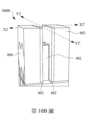
第3A圖、第4A圖、第9A圖、第10A圖和第12A圖提供根據第2圖的方法製造閘極全環(gate-all-around,GAA)裝置300A的等軸測(isometric)視圖。Figures 3A, 4A, 9A, 10A, and 12A provide isometric views of a gate-all-around (GAA)
第3B圖、第4B圖、第9B圖、第10B圖和第12B圖提供根據第2圖的方法製造鰭式場效電晶體裝置300B的等軸測視圖。Figures 3B, 4B, 9B, 10B, and 12B provide isometric views of a fin field
第5A圖、第5B圖、第7A圖和第7B圖提供鰭式場效電晶體裝置300B沿著平行於如第4B圖所示的剖面Y1-Y1'的平面的剖面圖。Figures 5A, 5B, 7A and 7B provide cross-sectional views of the fin field
第6A圖、第6B圖、第8A圖、第8B圖和第8C圖提供鰭式場效電晶體裝置300B沿著平行於如第4B圖所示的剖面X1-X1'的平面的剖面圖。Figures 6A, 6B, 8A, 8B and 8C provide cross-sectional views of the fin field
第10C圖和第10D圖分別提供閘極全環裝置300A和鰭式場效電晶體裝置300B沿著平行於如第10A圖和第10B圖所示的剖面X2-X2'的平面的剖面圖。FIG. 10C and FIG. 10D provide cross-sectional views of the gate
第10E圖和第10F圖分別提供閘極全環裝置300A和鰭式場效電晶體裝置300B沿著平行於如第10A圖和第10B圖所示的剖面Y2-Y2'的平面的剖面圖。FIG. 10E and FIG. 10F provide cross-sectional views of the gate
第11A圖和第11B圖提供如第10E圖所示的部分閘極全環裝置300A的放大視圖。Figures 11A and 11B provide enlarged views of a partial gate
第12C圖提供閘極全環裝置300A沿著平行於如第10A圖所示的剖面X2-X2'的平面的剖面圖。FIG. 12C provides a cross-sectional view of the gate
第12D圖提供鰭式場效電晶體裝置300B沿著平行於如第10B圖所示的剖面X2-X2'的平面的剖面圖。FIG. 12D provides a cross-sectional view of the fin field
第12E圖提供閘極全環裝置300A沿著平行於如第10A圖所示的剖面Y2-Y2'的平面的剖面圖。FIG. 12E provides a cross-sectional view of the gate
第12F圖提供第12E圖的一部分的放大剖面視圖,以更清楚地說明閘極全環裝置300A的各個方面的結構和尺寸。FIG. 12F provides an enlarged cross-sectional view of a portion of FIG. 12E to more clearly illustrate the structure and dimensions of various aspects of the gate
第12G圖提供鰭式場效電晶體裝置300B沿著平行於如第10B圖所示的剖面Y2-Y2'的平面的剖面圖。FIG. 12G provides a cross-sectional view of the fin field
以下揭示內容提供許多不同的實施方式或示例,用於實現所提供標的的不同特徵。下文描述元件和配置的具體示例以簡化本揭示內容。當然,這些只是示例,並不意欲限制。例如,在隨後的描述中,在第二特徵之上或上形成第一特徵可以包括其中第一特徵和第二特徵是直接接觸以形成的實施方式,也可以包括在第一特徵和第二特徵之間可形成附加特徵的實施方式,使得第一特徵和第二特徵可能不直接接觸。此外,本揭示內容可以在一些示例中重複附圖標記和/或字母。這種重複是為了簡單明瞭,本身並不限定所討論的一些實施方式和/或配置之間的關係。The following disclosure provides many different implementations or examples for implementing different features of the subject matter provided. Specific examples of components and configurations are described below to simplify the disclosure. Of course, these are examples and are not intended to be limiting. For example, in the subsequent description, forming a first feature on or over a second feature may include implementations in which the first feature and the second feature are directly in contact to form, and may also include implementations in which additional features may be formed between the first feature and the second feature, such that the first feature and the second feature may not be in direct contact. In addition, the disclosure may repeat figure labels and/or letters in some examples. This repetition is for simplicity and clarity and does not in itself limit the relationship between some of the implementations and/or configurations discussed.
此外,空間相對用語,例如「下面」、「下方」、「下」、「上面」、「上方」等,可在本文中使用以便於描述一個元素或特徵與圖中所示另一個元素或特徵的關係。空間相對用語旨在包括除圖中描述的方向之外,使用或操作中的裝置的不同方向。裝置可以其它方式定向(旋轉90度或其它方向),且本文使用的空間相對用語可同樣地對應解釋。Additionally, spatially relative terms, such as "below," "beneath," "below," "above," "above," etc., may be used herein to facilitate describing the relationship of one element or feature to another element or feature as depicted in a figure. Spatially relative terms are intended to encompass different orientations of the device in use or operation in addition to the orientation depicted in the figure. The device may be otherwise oriented (rotated 90 degrees or otherwise), and the spatially relative terms used herein may be interpreted accordingly.
更進一步地,當用「大約」、「近似」等描述一個數值或數值範圍時,此用語旨在包括所描述的數值及其包括在內的合理範圍內的數值,例如在所描述的數值的+/-10%以內或所屬技術領域中通常知識者理解的其它數值。例如,用語「約5nm」包括從4.5nm到5.5nm的尺寸範圍。Furthermore, when "approximately", "approximately", etc. are used to describe a value or a range of values, such terms are intended to include the described value and values within a reasonable range thereof, such as within +/-10% of the described value or other values understood by a person of ordinary skill in the art. For example, the term "about 5 nm" includes a size range from 4.5 nm to 5.5 nm.
還需注意的是,本揭示內容實施方式中的方法和相關結構是以可用於各種裝置類型中的任何一種的方式來呈現。例如本揭示內容的實施方式可用於製造平面的體金屬氧化物半導體場效電晶體(bulk metal-oxide-semiconductor field-effect transistor,bulk MOSFET)、多閘極電晶體(平面的或垂直的),例如鰭式場效電晶體裝置、閘極全環(GAA)裝置、Ω閘極裝置或Π閘極裝置、以及應變半導體裝置、絕緣體上矽(silicon-on-insulator,SOI)裝置、部分空乏型(partially-depleted)SOI裝置或其他所屬技術領域中已知的裝置。此外,本文揭示的實施方式可用於形成P型和/或N型裝置。所屬技術領域中通常知識者可能認知到半導體裝置的其它實施方式,這些實施方式可能受益於本揭示內容的各個方面。It is also noted that the methods and related structures of the embodiments of the present disclosure are presented in a manner that can be used in any of a variety of device types. For example, the embodiments of the present disclosure can be used to fabricate planar bulk metal-oxide-semiconductor field-effect transistors (bulk MOSFETs), multi-gate transistors (planar or vertical), such as fin field effect transistor devices, gate-all-around (GAA) devices, Ω-gate devices, or Π-gate devices, as well as strained semiconductor devices, silicon-on-insulator (SOI) devices, partially-depleted SOI devices, or other devices known in the art. In addition, the embodiments disclosed herein can be used to form P-type and/or N-type devices. A person of ordinary skill in the art may recognize other implementations of semiconductor devices that may benefit from aspects of this disclosure.
在先進的半導體加工中,製造具有低密度的介面阱和氧化物阱的電晶體對於提供高性能的裝置至關重要。然而隨著IC尺寸的不斷縮小和多閘極裝置(例如鰭式場效電晶體)的引入,挑戰也隨之增加。其中一個挑戰是雜訊,例如閃爍(1/f)雜訊,其可由介面阱和氧化物阱引起,並且會降低裝置性能。此外,鑒於多閘極裝置的電晶體的通道至閘極介電介面的表面積增加,在通道至閘極介電介面處載流子的電荷被捕捉的機會增加。因此現有技術並非在所有方面都完全令人滿意。In advanced semiconductor processing, fabricating transistors with low density of interface wells and oxide wells is critical to providing high performance devices. However, with the continuous reduction of IC size and the introduction of multi-gate devices (such as fin field effect transistors), challenges have also increased. One of the challenges is noise, such as flicker (1/f) noise, which can be caused by interface wells and oxide wells and degrade device performance. In addition, given the increased surface area of the channel-to-gate dielectric interface of the transistor of the multi-gate device, the chance of carrier charge being trapped at the channel-to-gate dielectric interface increases. Therefore, the existing technology is not completely satisfactory in all aspects.
本揭示內容的實施方式提供優於現有技術的優點,儘管可理解的是,其它實施方式可能提供不同的優點,且並非所有優點都必然在本文中討論,且並非所有實施方式具有特定優點。例如,本文討論的實施方式包括用於降低先進電晶體結構中雜訊(例如閃爍雜訊)的方法和結構。通常來說,本文揭示的實施方式可有效地降低閃爍雜訊,藉由改善(降低)介面阱和氧化物阱的密度,以及藉由調節電晶體通道電流路徑(例如電晶體的源極和汲極之間的電流路徑)以使電流路徑與電晶體的通道至閘極介電介面之間距離一距離,因此最大限度地減少通道至閘極介電介面處電荷遭受阱捕捉的機率。在一些實施方式中,阱的減少可以藉由使用沉積後退火(post-deposition anneal,PDA)製程(例如在形成閘極介電質之後執行)來達成,其中沉積後退火製程在氮氣(N2)環境中以PDA浸泡溫度為約攝氏80度至150度來執行。沉積後退火製程可能具有填充氧化物空位的效果,從而減少氧化物的捕捉中心。在一些實施中,阱的減少可以藉由使用TiN層(例如TiN覆蓋層)來減少閘極介電質對氧氣的吸收並減少氧化物缺陷。Implementations of the present disclosure provide advantages over the prior art, although it is understood that other implementations may provide different advantages, and not all advantages are necessarily discussed herein, and not all implementations have a particular advantage. For example, implementations discussed herein include methods and structures for reducing noise (e.g., flicker noise) in advanced transistor structures. Generally speaking, the embodiments disclosed herein can effectively reduce flash noise by improving (reducing) the density of interface wells and oxide wells, and by adjusting the transistor channel current path (e.g., the current path between the source and drain of the transistor) so that the current path is a distance away from the channel-to-gate dielectric interface of the transistor, thereby minimizing the probability of charge being trapped by wells at the channel-to-gate dielectric interface. In some embodiments, trap reduction can be achieved by using a post-deposition anneal (PDA) process (e.g., performed after forming the gate dielectric), wherein the PDA process is performed in a nitrogen (N2 ) environment with a PDA soak temperature of about 80 degrees Celsius to 150 degrees Celsius. The PDA process may have the effect of filling oxide vacancies, thereby reducing oxide trapping centers. In some embodiments, trap reduction can be achieved by using a TiN layer (e.g., a TiN cap layer) to reduce oxygen absorption by the gate dielectric and reduce oxide defects.
在一些實施方式中,電流路徑可以藉由摻雜靠近通道至閘極介電介面的電晶體通道(例如半導體層)來遠離電晶體的通道至閘極介電介面。在一示例中,電晶體通道可以使用離子注入製程(ion implantation process)、擴散摻雜製程(diffusion doping process)、經原子層沉積(atomic layer deposition)的摻雜層及其接續的趨入退火(drive-in anneal)製程、電漿摻雜(plasma doping,PLAD)製程或其他適當的摻雜製程來進行摻雜。特別的是,摻雜製程可用於在靠近通道至閘極介電介面的半導體通道層中引入摻雜劑(例如N型摻雜劑、P型摻雜劑、帶電正離子或帶電負離子),且此引入的摻雜劑的類型與被引入的電晶體的類型相同(例如對於N型電晶體來說是N型摻雜劑或帶電負離子,以及對於P型電晶體來說是P型摻雜劑或帶電正離子)。因此,在一些示例中,電晶體可以埋入式通道電晶體來執行操作,其中工作期間中的電晶體中的電流將在源極和汲極之間的電晶體主體(bulk)部分(例如在鰭式場效電晶體裝置的鰭結構的主體部分內)流動且遠離通道至閘極介電介面。在一些實施方式中,當摻雜劑的種類包括引入到N型電晶體在通道至閘極介電介面附近的閘極介電質中的帶電負離子時,在電晶體通道中流動的電子可以被帶電負離子排斥而遠離通道至閘極介電介面。在另一示例中,當摻雜劑種類包括引入到P型電晶體在通道至閘極介電介面附近的閘極介電質中的帶電正離子時,在電晶體通道中流動的電洞可以被帶電正離子排斥而遠離通道至閘極介電介面。無論採用何種方法,電流路徑移動到遠離電晶體的通道至閘極介電介面一距離,因此減少通道至閘極介電介面處載流子的電荷被捕捉及相關的閃爍雜訊。其它實施方式和優點對於所屬技術領域中通常知識者在閱讀本揭示內容時應是顯而易見的。In some embodiments, the current path can be doped away from the channel-to-gate dielectric interface of the transistor by doping the transistor channel (e.g., semiconductor layer) near the channel-to-gate dielectric interface. In one example, the transistor channel can be doped using an ion implantation process, a diffusion doping process, a doping layer deposited by atomic layer deposition and a subsequent drive-in annealing process, a plasma doping (PLAD) process, or other suitable doping processes. In particular, the doping process can be used to introduce a dopant (e.g., an N-type dopant, a P-type dopant, positively charged ions, or negatively charged ions) into a semiconductor channel layer near a channel-to-gate dielectric interface, and the type of dopant introduced is the same as the type of transistor being introduced (e.g., an N-type dopant or negatively charged ions for an N-type transistor, and a P-type dopant or positively charged ions for a P-type transistor). Thus, in some examples, the transistor may be operated as a buried channel transistor, wherein the current in the transistor during operation will flow in the bulk portion of the transistor between the source and drain (e.g., within the bulk portion of the fin structure of a fin field effect transistor device) and away from the channel to gate dielectric interface. In some embodiments, when the type of dopant includes negatively charged ions introduced into the gate dielectric of the N-type transistor near the channel to gate dielectric interface, electrons flowing in the transistor channel may be repelled by the negatively charged ions away from the channel to gate dielectric interface. In another example, when the dopant species includes charged positive ions introduced into the gate dielectric of a P-type transistor near the channel-to-gate dielectric interface, holes flowing in the transistor channel can be repelled by the charged positive ions away from the channel-to-gate dielectric interface. Regardless of the method used, the current path moves to a distance away from the channel-to-gate dielectric interface of the transistor, thereby reducing the charge capture of carriers at the channel-to-gate dielectric interface and the associated flicker noise. Other embodiments and advantages should be apparent to those of ordinary skill in the art upon reading this disclosure.
現在參照第1A圖的示例,示出金屬氧化物半導體(MOS)的電晶體100,作為可包括本揭示內容實施方式的一種裝置類型的示例。可以理解的是,示例性的電晶體100並不意欲以任何方式進行限制,並且所屬技術領域中通常知識者將認識到,本揭示內容的實施方式可同樣適用於其它各種裝置類型中的任何一種,例如上文描述的那些。電晶體100在基板102上製造且包括閘極堆疊104。基板102可以是半導體基板,例如矽基板。基板102可以包括各種層,包括在基板102上形成的導電層或絕緣層。基板102可以包括各種摻雜的配置,取決於所屬技術領域中已知的設計需求。基板102還可以包括其它半導體,例如鍺、碳化矽(SiC)、矽鍺(SiGe)或鑽石。可選地,基板102可以包括化合物半導體和/或合金半導體。此外,在一些實施方式中,基板102可以包括磊晶層(epitaxial layer,epi-layer),基板102可被施加應變以增強性能,基板102可以包括絕緣體上矽(SOI)結構,和/或基板102可以具有其它合適的增強特徵。Referring now to the example of FIG. 1A , a metal oxide semiconductor (MOS)
閘極堆疊104包括閘極介電質106及設置在閘極介電質106上的閘極電極108。在一些實施方式中,閘極介電質106可以包括諸如氧化矽(SiO2)層或氮氧化矽(SiON)的介面層,這種介面層可以藉由化學氧化、熱氧化、原子層沉積(ALD)、化學氣相沉積(chemical vapor deposition,CVD)和/或其它合適的方法形成。在一些示例中,閘極介電質106包括高k值介電層,例如氧化鉿(HfO2)。或者,高k值介電層可以包括其它高k值介電質,例如TiO2、HfZrO、Ta2O3、HfSiO4、ZrO2、ZrSiO2、LaO、AlO、ZrO、TiO、Ta2O5、Y2O3、SrTiO3(STO)、BaTiO3(BTO)、BaZrO、HfZrO、HfLaO、HfSiO、LaSiO、AlSiO、HfTaO、HfTiO、(Ba,Sr)TiO3(BST)、Al2O3、Si3N4、氮氧化物(SiON)、其組合或其它合適的材料。本文使用和描述的高k值閘極介電質包括具有高介電常數的介電材料,例如大於熱氧化矽(~3.9)。在又一些實施方式中,閘極介電質106可以包括二氧化矽或其它合適的介電質。閘極介電質106可以藉由ALD、物理氣相沉積(physical vapor deposition,PVD)、CVD、氧化和/或其它合適的方法形成。在一些實施方式中,閘極電極108可以在前閘極(gate first)或後閘極(gate last,例如替換閘極)製程中的一部分中被沉積。在一些實施方式中,閘極電極108包括導電層,例如W、Ti、TiN、TiAl、TiAlN、Ta、TaN、WN、Re、Ir、Ru、Mo、Al、Cu、Co、CoSi、Ni、NiSi、其組合和/或其它合適的組成物。在一些示例中,閘極電極108可以包括用於N型電晶體的第一金屬材料和用於P型電晶體的第二金屬材料。因此,電晶體100可以包括雙功函數(dual work-function)的金屬閘極配置。例如,第一金屬材料(例如用於N型裝置)可以包括具有與基板導帶的功函數基本上一致的功函數,或至少與電晶體100的通道區域114的導帶的功函數基本上一致。類似地,第二金屬材料(例如用於P型裝置)可以包括具有與基板價帶的功函數基本上一致的功函數,或至少與電晶體100的通道區域114的價帶的功函數基本上一致。因此,閘極電極108可為包括N型和P型裝置的電晶體100提供閘極電極。在一些實施方式中,閘極電極108可替代性地或附加性地包括多晶矽層。在一些示例中,閘極電極108可以使用PVD、CVD、電子束(electron beam,e-beam)蒸發和/或其它合適的製程形成。在一些實施方式中,側壁間隙物形成在閘極堆疊104的側壁上。這種側壁間隙物可以包括介電材料,例如氧化矽、氮化矽、碳化矽、氮氧化矽或其組合。The
電晶體100還包括源極區域110和汲極區域112,各自形成在半導體的基板102內,並且相鄰及位於閘極堆疊104的任一側。在一些實施方式中,源極區域110和汲極區域112包括擴散的源極/汲極區域、離子注入源極/汲極區域、磊晶生長區域或其組合。電晶體100的通道區域114被定義為在閘極介電質106下及半導體的基板102內的源極區域110與汲極區域112之間的區域。通道區域114具有通道長度L和通道寬度W。在操作時,電流(例如電晶體驅動的電流)藉由通道區域114在源極區域110和汲極區域112之間流動。針對給定的偏壓(例如施加到閘極電極108或源極區域110與汲極區域112之間)而引發的驅動電流的量是用於形成通道區域114的材料的遷移率等的函數。在一些示例中,通道區域114包括矽(Si)和/或高遷移率材料,例如鍺,其可以磊晶生長而成,以及包括所屬技術領域中已知的多種化合物半導體或合金半導體中的任何一種。高遷移率材料包括具有電子和/或電洞遷移率大於矽(Si)的材料,其中矽在室溫(300K)下的本徵(intrinsic)電子遷移率為約1350cm2/V-s,以及在室溫(300K)下的本徵(intrinsic)電洞遷移率為約480cm2/V-s。The
參照第1B圖,示出的是多閘極裝置150,提供本揭示內容實施方式的替代性的裝置類型的示例。作為示例,多閘極裝置150包括一個或多個多閘極場效電晶體(field-effect transistor,FET)。在一些實施方式中,多閘極裝置150可以包括鰭式場效電晶體裝置或閘極全環裝置。多閘極裝置150包括基板152、從基板152延伸的至少一個鰭154、隔離區域156以及設置在鰭154上和周圍的閘極結構158。基板152可以是半導體基板,例如矽基板。在一些實施方式中,基板152可與基板102基本上相同且可包括用於基板102的一種或多種材料,如上文所述。Referring to FIG. 1B , a
鰭154與基板152一樣,可包括一個或多個磊晶生長層,並且可以包括矽或其他元素半導體,例如鍺;化合物半導體,包括碳化矽、砷化鎵、磷化鎵、磷化銦、砷化銦和/或銻化銦;合金半導體,包括SiGe、GaAsP、AlInAs、AlGaAs、InGaAs、GaInP和/或GaInAsP;或其組合。鰭154可以使用合適的製程製造,包括微影和蝕刻製程。微影製程可能包括在基板上(例如在矽層上)形成光阻(photoresist或resist)層、將光阻層暴露於圖案中、執行暴露後烘烤製程以及顯影光阻劑,以形成包括光阻劑的遮罩元件。在一些實施方式中,可以使用電子束(e-beam)微影製程對光阻層執行圖案化以形成遮罩元件。然後可以使用遮罩元件來保護基板的多個區域,同時使用蝕刻製程在矽層中形成溝槽,從而留下延伸的鰭154。溝槽可以使用乾蝕刻(例如化學氧化物移除)、濕蝕刻和/或其他合適的製程來執行蝕刻。還可以使用其他在基板152上形成鰭154的實施方式。還需注意的是,當多閘極裝置150包括鰭式場效電晶體裝置時,鰭154可以包括組成基本上均勻的連續鰭,以及當多閘極裝置150包括閘極全環裝置時,鰭154可以包括由閘極結構158的多個部分插置之間的多個半導體通道層中的多個通道。
這些鰭154中的每一個還包括源極區域155和汲極區域157,其中源極區域155/汲極區域157形成在鰭154中、上和/或周圍。源極區域155/汲極區域157可以磊晶生長在鰭154上。此外,電晶體的通道區域(或多個通道區域)沿著基本上平行於由第1B圖的剖面A-A'定義的平面設置在鰭154中及閘極結構158的底層。在一些示例中,鰭的通道區域包括高遷移率材料,如上文所述。Each of these
隔離區域156可以是淺溝槽隔離(shallow trench isolation,STI)特徵。替代性地,場氧化物(field oxide)、LOCOS特徵和/或其它合適的隔離特徵可以在基板152上和/或內實施。隔離區域156可以由氧化矽、氮化矽、氮氧化矽、氟摻雜矽酸鹽玻璃(fluorine-doped silicate glass,FSG)、低k值介電質、其組合和/或所屬技術領域中已知的其它合適材料組成。在一實施方式中,隔離區域156是淺溝槽隔離特徵,並且藉由在基板152中蝕刻溝槽而形成。然後可以用隔離材料填充溝槽,接著執行化學機械拋光(chemical mechanical polishing,CMP)製程。然而,其它實施方式也是可能的。在一些實施方式中,隔離區域156可以包括多層結構,例如具有一個或多個襯層。The
閘極結構158包括具有在鰭154的通道區域上形成介面層160的閘極堆疊、在介面層160上形成的閘極介電層162,以及在閘極介電層162上形成的金屬層164。在一些實施方式中,介面層160基本上與被描述為閘極介電質106一部分的介面層相同。在一些實施方式中,閘極介電層162基本上與閘極介電質106相同,並且可以包括類似於用於閘極介電質106的高k值介電質。類似地,在一些實施方式中,金屬層164基本上與上述閘極電極108相同。在一些實施方式中,側壁間隙物形成在閘極結構158的側壁上。側壁間隙物可以包括介電材料,例如氧化矽、氮化矽、碳化矽、氮氧化矽或其組合。The
每個電晶體100和多閘極裝置150可以包括本揭示內容的一個或多個實施方式,且在下文中更詳細地描述。然而,為了清楚起見,下文的討論主要針對多閘極裝置,例如多閘極裝置150。本文所用的用語「多閘極裝置」用於描述具有至少一些閘極材料設置在裝置的至少一個通道的多個側面上的裝置(例如半導體電晶體)。例如,多閘極裝置可以包括具有閘極材料設置在電晶體通道的至少三個側面上的鰭式場效電晶體裝置、具有閘極材料設置在電晶體通道的至少四個側面上的閘極全環裝置,或是閘極全環裝置與鰭式場效電晶體裝置一起形成的組合。當多閘極裝置包括閘極全環裝置時,通道區域可稱為「奈米線」且包括各種幾何形狀(例如圓柱形、條形)和各種尺寸的通道區域。Each
參照第2圖,示出半導體製造的方法200,包括製造包括閘極全環裝置300A和鰭式場效電晶體裝置300B的多閘極裝置。可以理解的是,方法200包括具有互補式金屬氧化物半導體(CMOS)技術製程流程特徵的步驟,因此在此僅簡要描述。附加步驟可在方法200之前、之後和/或之間執行。需要注意的是,閘極全環裝置300A和鰭式場效電晶體裝置300B可以包括各種其它裝置和特徵,例如其他類型的裝置,諸如附加的電晶體、雙極性接面電晶體(bipolar junction transistor)、電阻器、電容器、電感器、二極體、保險絲、靜態隨機存取記憶體(static random-access memory,SRAM)和/或其它邏輯電路等,但為更好地理解本揭示內容的概念而在本揭示內容中被簡化。在一些實施方式中,閘極全環裝置300A和鰭式場效電晶體裝置300B包括複數個半導體裝置(例如電晶體),包括PFET、NFET等,且它們可以互連。此外,需要注意的是,方法200的製程步驟,以及包括參照附圖的任何描述僅是示例性的,並不意欲限制隨後申請專利範圍中具體記載的內容。Referring to FIG. 2 , a
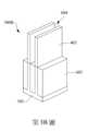
方法200從提供部分已經製造的多閘極裝置的方塊202開始。參照第3A圖和第3B圖的示例,在方塊202的實施方式中,部分已經製造的多閘極裝置可以包括如第3A圖所示的部分已經製造的閘極全環裝置300A,或如第3B圖所示的部分已經製造的鰭式場效電晶體裝置300B。根據一些實施方式,第3A圖和第3B圖分別提供閘極全環裝置300A和鰭式場效電晶體裝置300B的等軸測視圖。出於討論的目的,將並行討論閘極全環裝置300A和鰭式場效電晶體裝置300B的製造製程。然而可以理解的是,在一些實施方式中,一種裝置類型或兩種裝置類型(閘極全環裝置和/或鰭式場效電晶體裝置)可以在一個給定的基板上被製造。每個閘極全環裝置300A和鰭式場效電晶體裝置300B包括基板302。在一些實施方式中,基板302可以是諸如矽基板的半導體基板。在一些實施方式中,基板302可以與基板102、基板152基本上相同,並且可以包括用於基板102、基板152的一種或多種材料,如上文所述。此外,閘極全環裝置300A和鰭式場效電晶體裝置300B中的每個可以包括在基板302的N型區域形成的N型裝置或在基板302的P型區域形成的P型裝置。The
如第3A圖所示,閘極全環裝置300A包括從基板302延伸的鰭602,其中鰭602包括基板部分以及基板部分上具有第二組成物的磊晶層308插置其間的第一組成物的磊晶層306。第一組成物和第二組成物可以不同。在一實施方式中,磊晶層306是SiGe,以及磊晶層308是矽(Si)。其它實施方式也是可能的,包括那些使第一組成物和第二組成物具有不同氧化速率和/或蝕刻選擇性的實施方式。磊晶層308或其部分可形成閘極全環裝置300A的通道區域。例如,磊晶層308可被稱為「奈米線」,用於形成閘極全環裝置300A的通道區域。這些「奈米線」也可用於形成閘極全環裝置300A的源極/汲極特徵的一部分。同樣地,如本文中使用的用語,「奈米線」是指圓柱形的半導體層以及諸如條形的其它構形。As shown in FIG. 3A , the gate all around
需要注意的是,雖然7層磊晶層306和6層磊晶層308在第3A圖中示出,但這僅用於說明的目的,並不意欲限制申請專利範圍中具體記載的內容。可以理解的是,可以形成任意數量的磊晶層;層數取決於閘極全環裝置300A所需的通道區域數量。在一些實施方式中,磊晶層308的數量在4和10之間。It should be noted that although 7
在一些實施方式中,磊晶層306具有約4奈米至8奈米(nm)的厚度範圍。在一些實施方式中,磊晶層306的厚度可以基本上均勻。然而在一些實施中,磊晶層306的最頂層可以比其餘磊晶層306厚,例如以減輕在隨後CMP製程中可能發生的磊晶層306的最頂層的損失。在一些實施方式中,磊晶層308具有約5奈米至8奈米的厚度範圍。在一些實施方式中,磊晶層308的厚度基本上均勻。如下文更詳細地描述,磊晶層308可用作隨後形成的閘極全環裝置300A的通道區域,並根據裝置性能考慮選擇的厚度。磊晶層306可用於為隨後形成的多閘極裝置定義相鄰通道區域之間的間隙距離,並根據裝置性能考慮選擇的厚度。In some embodiments, the
作為示例,磊晶層306和磊晶層308的磊晶生長可以藉由分子束磊晶(molecular beam epitaxy,MBE)製程、金屬有機化學氣相沉積(metalorganic chemical vapor deposition,MOCVD)製程和/或其它合適的磊晶生長製程來實現。在一些實施方式中,磊晶生長層例如磊晶層308包括與基板302相同的材料。在一些實施方式中,磊晶生長的磊晶層306及磊晶層308包括與基板302不同的材料。如上文所述,在至少一些示例中,磊晶層306包括磊晶生長的矽鍺(SiGe)層,以及磊晶層308包括磊晶生長的矽(Si)層。或者,在一些實施方式中,磊晶層306和磊晶層308中的任何一者可以包括其它材料,例如鍺;如碳化矽、砷化鎵、磷化鎵、磷化銦、砷化銦的化合物半導體;如SiGe、GaAsP、AlInAs、AlGaAs、InGaAs、GaInP和/或GaInAsP的合金半導體;或其組合。如前文所述,磊晶層306和磊晶層308的材料可以基於提供不同氧化、蝕刻速率和/或蝕刻選擇性的特性來選擇。在一些實施方式中,磊晶層306和磊晶層308起初基本上不含摻雜劑(即,具有約0cm-3至約1x1017cm-3的外來(extrinsic)摻雜劑濃度),例如在磊晶生長製程中不有意地執行摻雜。然而如下文所述並按照本揭示內容的實施方式,磊晶層308靠近磊晶層308表面的部分(例如在通道至閘極介電介面處)可以被有意地摻雜,以便電流路徑(例如在源極和汲極之間)被移動一段距離(例如大於約2Å)至遠離電晶體的通道至閘極介電介面。可以肯定的是,在一些示例中,磊晶層308表面附近的磊晶層308的部分可以在磊晶層308的磊晶生長製程中被原位摻雜。As an example, the epitaxial growth of
如第3B圖所示,鰭式場效電晶體裝置300B包括從基板302延伸的鰭604,其中鰭604包括基板部分和在基板部分上形成的磊晶層402。在一些實施方式中,磊晶層402包括Si或SiGe;然而其它實施方式也是可能的。在磊晶層402包括SiGe的實施方式中,SiGe中Ge的百分比可以在約0%至35%之間。磊晶層402或其部分可以形成鰭式場效電晶體裝置300B的通道區域。磊晶層402或其部分也可用於形成鰭式場效電晶體裝置300B部分的源極/汲極特徵,如下文所述。As shown in FIG. 3B , the fin field
與磊晶層306及磊晶層308類似,磊晶層402的磊晶生長可以藉由MBE製程、MOCVD製程和/或其它合適的磊晶生長製程來實現。在一些實施方式中,磊晶層402可以包括與基板302相同的材料。在一些實施方式中,磊晶層402可以包括與基板302不同的材料。如上文所述,在至少一些示例中,磊晶層402包括磊晶生長的矽或矽鍺(SiGe)層。或者,在一些實施方式中,磊晶層402可以包括其它材料,例如鍺;如碳化矽、砷化鎵、磷化鎵、磷化銦、砷化銦和/或銻化銦的化合物半導體;如SiGe、GaAsP、AlInAs、AlGaAs、InGaAs、GaInP和/或GaInAsP的合金半導體;或其組合。在一些實施方式中,磊晶層402起初基本上不含摻雜劑(即,具有約0cm-3至約1x1017cm-3的外來摻雜劑濃度),例如在磊晶生長製程中不執行有意的摻雜。然而如下面討論的,且根據本揭示內容的實施方式,磊晶層402靠近磊晶層402表面的部分(例如在通道至閘極介電介面處)可以有意地摻雜,以使電流路徑(例如在源極和汲極之間)遠離電晶體的通道至閘極介電介面一段距離(例如大於約2Å)。Similar to
在一些實施方式中,鰭602和鰭604可以使用合適的製程製造,包括微影和蝕刻製程,並且以基本上類似於上述參照多閘極裝置150的鰭154的方式製造。在形成鰭602和鰭604時,可以在鰭602和鰭604附近形成插置其間的溝槽。在一些實施方式中,溝槽可以介電材料填充,然後可以將其平坦化和凹陷,以形成淺溝槽隔離特徵。在一些實施方式中,用於填充溝槽的介電層可以包括SiO2、氮化矽、氮氧化矽、氟摻雜矽酸鹽玻璃(FSG)、低k值介電質、其組合和/或所屬技術領域中已知的其它合適材料。在一些示例中,介電層可以藉由CVD製程、次大氣壓CVD(subatmospheric CVD,SACVD)製程、流動式CVD製程、ALD製程、PVD製程和/或其他合適的製程沉積。在一些實施方式中,閘極全環裝置300A、鰭式場效電晶體裝置300B可以例如藉由退火以提高介電層的品質。在一些實施方式中,介電層(以及因此淺溝槽隔離特徵)可以包括多層結構,例如具有一個或多個襯層。In some embodiments,
如第3A圖和第3B圖的示例所示,淺溝槽隔離特徵凹陷,使得鰭602和鰭604延伸到淺溝槽隔離特徵上方。在一些實施方式中,凹陷製程可以包括乾蝕刻製程、濕蝕刻製程和/或其組合。在一些實施方式中,凹陷深度被控制(例如藉由控制蝕刻時間)以使鰭602和鰭604的上部暴露所需高度。在一些實施方式中,此高度暴露閘極全環裝置300A中的每個磊晶層306和磊晶層308以及基本上鰭式場效電晶體裝置300B中全部的磊晶層402。As shown in the examples of FIGS. 3A and 3B , the shallow trench isolation feature is recessed so that
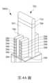
然後方法200繼續到形成虛擬閘極結構的方塊204。雖然目前的討論是針對替換閘極(後閘極)製程,其中虛擬閘極結構被形成並隨後被替換,但其他配置(例如先閘極)也可能是可行的。參照第4A圖和第4B圖,在方塊204的實施方式中,在閘極全環裝置300A的鰭602上形成閘極堆疊702,並且在鰭式場效電晶體裝置300B的鰭604上形成閘極堆疊704。根據一些實施方式,第4A圖和第4B圖分別提供閘極全環裝置300A和鰭式場效電晶體裝置300B的等軸測視圖。在一實施方式中,閘極堆疊702和閘極堆疊704是隨後被移除和替換的虛擬(犧牲)閘極堆疊,如下文所述。The
在一些實施方式中,在形成閘極堆疊702和閘極堆疊704之前,可任選地形成介電層706。在一些實施方式中,介電層706沉積在基板302、鰭602和鰭604上,包括在相鄰鰭602和鰭604之間的溝槽中。在一些實施方式中,介電層706可以包括SiO2、氮化矽、高k值介電材料或其它合適的材料。在不同的示例中,介電層706可以藉由CVD製程、次大氣壓CVD(SACVD)製程、流動式CVD製程、ALD製程、PVD製程或其它合適的製程沉積。作為示例,介電層706可用於防止後續製程(例如隨後的虛擬閘極的形成)損壞鰭602和鰭604。In some embodiments, a
在一些使用後閘極製程的實施方式中,閘極堆疊702和閘極堆疊704是虛擬閘極堆疊,並且在閘極全環裝置300A和鰭式場效電晶體裝置300B的後續製程階段中被最終的閘極堆疊取代。特別地是,閘極堆疊702和閘極堆疊704可以在後續的製程階段中被高k值介電層(high-k,HK)和金屬閘極(metal gate electrode,MG)取代。在一些實施方式中,閘極堆疊702和閘極堆疊704形成在基板302上並且至少部分地設置在鰭602和鰭604上。此外,在一些實施方式中,閘極堆疊702和閘極堆疊704可以在介電層706上形成,介電層706任選地在形成閘極堆疊702和閘極堆疊704之前如上文所述沉積。鰭602和鰭604在閘極堆疊702和閘極堆疊704下方的部分可稱為通道區域。閘極堆疊702和閘極堆疊704還可以定義鰭602和鰭604的源極/汲極區域,例如鰭602和鰭604相鄰通道區域且在通道區域相對側的部分。In some embodiments using a gate-last process, the
在一些實施方式中,閘極堆疊702和閘極堆疊704包括介電層和電極層,兩者均由元件707示意。閘極堆疊702和閘極堆疊704還可以包括一個或多個硬遮罩層708和硬遮罩層710。在一些實施方式中,硬遮罩層708可以包括氧化物層,並且硬遮罩層710可以包括氮化物層。在一些實施方式中,閘極堆疊702和閘極堆疊704藉由各種製程步驟形成,例如層沉積、圖案化、蝕刻,以及其它合適的製程步驟。在一些示例中,層沉積製程包括CVD(包括低壓CVD和電漿增強CVD)、PVD、ALD、熱氧化、電子束蒸發或其它合適的沉積技術,或其組合。在形成閘極堆疊時,例如圖案化製程包括微影製程(例如微影或電子束微影),其還可以包括光阻劑塗層(例如旋轉塗佈)、軟烘烤、遮罩對準、暴露、暴露後烘烤、顯影光阻劑、潤洗、乾燥(例如旋乾和/或硬烘烤)、其它合適的微影技術和/或其組合。在一些實施方式中,蝕刻製程可包括乾蝕刻(例如RIE蝕刻)、濕蝕刻和/或其它蝕刻方法。In some embodiments,
在一些實施方式中,閘極堆疊702和閘極堆疊704中的介電層包括氧化矽。替代地或附加地,閘極堆疊702和閘極堆疊704中的介電層可以包括氮化矽、高k值介電材料或其它合適的材料。在一些實施方式中,閘極堆疊702和閘極堆疊704中的電極層可以包括多晶矽(polysilicon)。在一些實施方式中,硬遮罩層708的氧化物包括可包括SiO2的墊氧化層。在一些實施方式中,硬遮罩層710的氮化物包括可包括Si3N4、氮氧化矽或碳化矽的墊氮化物層。In some embodiments, the dielectric layer in the
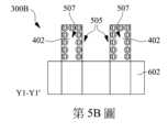
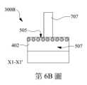
然後方法200繼續到方塊206,執行第一通道摻雜製程。參照第5A圖、第5B圖、第6A圖、第6B圖、第7A圖、第7B圖、第8A圖、第8B圖和第8C圖,在方塊206的實施方式中,對鰭式場效電晶體裝置300B執行第一通道摻雜製程。第5A圖、第5B圖、第7A圖、第7B圖提供鰭式場效電晶體裝置300B沿著平行於剖面Y1-Y1'的平面的剖面圖,以及第6A圖、第6B圖、第8A圖、第8B圖、第8C圖提供鰭式場效電晶體裝置300B沿著平行於剖面X1-X1'的平面的剖面圖,如第4B圖所示。在一示例中,磊晶層402靠近磊晶層402表面的部分(例如靠近將成為通道至閘極介電介面的地方)可以被有意地摻雜,以使電流路徑(例如在源極和汲極之間)被移動至遠離電晶體的通道至閘極介電介面一距離(例如大於約2Å)。閘極全環裝置300A靠近磊晶層308表面的磊晶層308的部分(例如形成閘極全環裝置300A的通道者)可在製程的後期階段摻雜,如下文進一步的描述。需要注意的是,介電層706雖為了清楚起見而在第5A圖、第5B圖、第6A圖、第6B圖、第7A圖、第7B圖、第8A圖、第8B圖和第8C圖省略,但其可存在也可不存在,如下文中更詳細的描述。The
首先參照第5A圖、第5B圖、第6A圖和第6B圖,在方塊206中的一個實施方式中,可以執行離子注入製程502以沿著磊晶層402的表面及閘極堆疊704下方(例如元件707下方)形成摻雜層505。在一些示例中,離子注入製程502可以藉由上述介電層706來執行,或者離子注入製程502可以在介電層706形成之前執行或在不形成介電層706的情況執行。在第5B圖和第6B圖中,形成摻雜層505的摻雜劑圖示為字母「D」且位於圓圈內。注入能量、注入劑量、傾斜角度和旋轉被優化以使摻雜層505沿著磊晶層402的表面形成,如圖所示。特別地是,離子注入製程502可以被優化成穿透閘極堆疊704的至少下部,以便在閘極堆疊704下方形成摻雜層505。在一些實施方式中,摻雜層505的摻雜劑濃度可以在約1x1014cm-3至1x1015cm-3的範圍內,離子注入製程502的傾斜角度可以在約0°至40°之間(並且可以包括以不同的傾斜角度形成摻雜層505的多次注入),以及鰭式場效電晶體裝置300B可以在離子注入製程502期間旋轉以確保摻雜劑的均勻分佈。在一些實施中,在離子注入製程502期間,鰭式場效電晶體裝置300B可以連續或分離式的步驟進行旋轉(例如約0個至8個分離步驟)。需要注意的是,離子注入製程502在一些方面可以類似於輕摻雜汲極(lightly doped drai,LDD)注入製程,並且在一些實施中可以被稱為LDD注入,即使所得摻雜層505跨越包括閘極堆疊704下方的磊晶層402的表面。同樣地,在一些實施中,離子注入製程502可以包括電漿摻雜(PLAD)製程。Referring first to FIGS. 5A, 5B, 6A, and 6B, in one embodiment in
在一些實施方式中,用於形成摻雜層505的摻雜劑種類與將其引入的電晶體具有相同的類型(極性)(例如對於N型電晶體來說的N型摻雜劑種類或帶電負離子,以及對於P型電晶體來說的P型摻雜劑種類或帶電正離子)。以另一種方式說明,用於形成摻雜層505的摻雜劑種類可以與將其引入的裝置中的源極/汲極摻雜物質具有相同的類型(極性)(例如N型摻雜劑種類或帶電負離子用於具有N型源極/汲極的裝置,以及P型摻雜劑種類或帶電正離子用於具有P型源極/汲極的裝置)。雖然摻雜劑種類可以是相同的類型(極性),但需要注意的是,摻雜層505的摻雜劑濃度小於源極/汲極的摻雜劑濃度。作為示例,如果鰭式場效電晶體裝置300B是N型裝置,則離子注入製程502(以及所得摻雜層505)可以包括N型摻雜劑種類(例如如磷、砷、銻的第V欄元素和/或如帶負電的磷離子的帶電負離子)。在另一示例中,如果鰭式場效電晶體裝置300B是P型裝置,則離子注入製程502(以及所得摻雜層505)可以包括P型摻雜劑種類(例如如硼的第III欄元素和/或如帶正電荷的硼離子的帶電正離子)。在這種情況下,鰭式場效電晶體裝置300B可以類似於埋入式通道電晶體進行工作,其中在鰭式場效電晶體裝置300B的工作期間,電流主要流過鰭式場效電晶體裝置300B中源極和汲極之間的磊晶層402的主體部分507且遠離通道至閘極介電介面。在一些實施方式中,在摻雜層505形成之後,鰭式場效電晶體裝置300B可經高熱預算(thermal budget)製程(退火)移除缺陷並活化摻雜劑(即,將摻雜劑置於取代位點)。In some embodiments, the dopant species used to form the
現在參照第7A圖、第7B圖、第8A圖、第8B圖和第8C圖,在方塊206的另一個實施方式中,可以在磊晶層402上形成經原子層沉積的摻雜層509,例如在形成(或不形成)介電層706之前和在形成閘極堆疊704之前(例如如第8A圖所示)。經原子層沉積的摻雜層509可類似地用於沿著磊晶層402的表面及閘極堆疊704下方形成摻雜層505,如上文所述。在一些實施方式中,經原子層沉積的摻雜層509可以包括與將其引入的電晶體的類型(極性)相同的摻雜劑種類,或與將其引入的裝置中的源極/汲極摻類相同的類型(極性),如上文所述。作為示例,如果鰭式場效電晶體裝置300B是N型裝置,則經原子層沉積的摻雜層509可以包括N型摻雜劑物種(例如如磷、砷、銻的第V欄元素和/或如帶負電的磷離子的帶電負離子)。在另一示例中,如果鰭式場效電晶體裝置300B是P型裝置,則經原子層沉積的摻雜層509可以包括P型摻雜劑種類(例如如硼的第III欄元素和/或如帶正電的硼離子的帶電正離子)。在一些實施中,經原子層沉積的摻雜層509可以包括用於N型裝置的基於F的層(例如諸如WFx)和用於P型裝置的基於Al的層(例如諸如TiAl)。在沉積經原子層沉積的摻雜層509之後,可以執行趨入退火以使經原子層沉積的摻雜層509內的摻雜劑擴散到磊晶層402的表面以形成摻雜層505(例如如第8B圖所示)。在趨入退火之後,在一些實施中,經原子層沉積的摻雜層509的任何剩餘部分可以使用合適的蝕刻製程(例如濕蝕刻製程、乾蝕刻製程或其組合)移除。在本示例中,在形成摻雜層505之後,可以形成閘極堆疊704,如上文所述(例如如第8C圖所示)。同樣地,在一些實施中,不使用經原子層沉積的摻雜層509,而以電漿摻雜(PLAD)製程在形成閘極堆疊704之前形成摻雜層505。7A, 7B, 8A, 8B, and 8C, in another embodiment of
然後方法200繼續至形成間隙物元件的方塊208。參照第9A圖和第9B圖,在方塊208的實施方式中,側壁間隙物802形成在閘極堆疊702和閘極堆疊704的側壁上。根據一些實施方式,第9A圖和第9B圖分別提供閘極全環裝置300A和鰭式場效電晶體裝置300B的等軸測視圖。側壁間隙物802的形成可以包括在閘極全環裝置300A和鰭式場效電晶體裝置300B的每個上沉積間隙物材料層。在一些示例中,沉積間隙物材料層可以包括介電材料,例如氧化矽、氮化矽、碳化矽、氮氧化矽、SiCN薄膜、碳氧化矽、SiOCN薄膜和/或其組合。在一些實施方式中,間隙物材料層包括多層,例如主間隙物側壁、襯層等。作為示例,間隙物材料層可以藉由在閘極堆疊702和閘極堆疊704上沉積介電材料而形成,使用諸如CVD製程、次大氣壓CVD(SACVD)製程、流動式CVD製程、ALD製程、PVD製程或其它合適的製程。The
在一些實施方式中,沉積間隙物材料層之後是回蝕(例如各向異性)介電質的間隙物材料。參照第9A圖和第9B圖的示例,在形成間隙物材料層之後,間隙物材料層可以被回蝕以暴露與閘極堆疊702和閘極堆疊704相鄰且未被閘極堆疊702和閘極堆疊704覆蓋的鰭602和鰭604的部分(例如源極/汲極區域)。間隙物材料層可以保留在閘極堆疊702和閘極堆疊704的側壁上以形成側壁間隙物802。在一些實施方式中,間隙物材料層的回蝕可以包括濕蝕刻製程、乾蝕刻製程、多步蝕刻製程和/或其組合。間隙物材料層也可以從閘極堆疊702和閘極堆疊704的頂面移除,如第9A圖和第9B圖所示。In some embodiments, depositing the spacer material layer is followed by etching back the (e.g., anisotropic) dielectric spacer material. Referring to the examples of FIGS. 9A and 9B , after forming the spacer material layer, the spacer material layer may be etched back to expose portions of the
然後,方法200繼續方塊210,形成源極/汲極特徵。最初,在方塊210的實施方式中,在形成閘極堆疊702和閘極堆疊704和/或側壁間隙物802之後,介電層706(第4A圖或第4B圖)如果存在的話可以被回蝕以暴露鰭602和鰭604未被閘極堆疊702和閘極堆疊704覆蓋的部分(例如在源極/汲極區域中),包括磊晶層306、磊晶層308和磊晶層402的一部分。在一些示例中,介電層706可以基本上被回蝕刻至底下的淺溝槽隔離特徵。在一些實施方式中,介電層706的回蝕可以包括濕蝕刻製程、乾蝕刻製程、多步蝕刻製程和/或其組合。因此在一些實施方式中,在閘極堆疊702和閘極堆疊704的形成過程中保留介電層706可用於在製程期間有效地保護鰭602和鰭604。Then, the
再次參照第9A圖和第9B圖的示例,在方塊210的進一步實施方式中,源極/汲極特徵804和源極/汲極特徵806形成於與閘極堆疊702和閘極堆疊704相鄰的源極/汲極區域及閘極堆疊702和閘極堆疊704兩側。在一些實施方式中,源極/汲極特徵804和源極/汲極特徵806是藉由在源極/汲極區域暴露的鰭602和鰭604上磊晶生長半導體材料層而形成。在一些實施方式中,生長形成源極/汲極特徵804和源極/汲極特徵806的半導體材料層可以包括Ge、Si、GaAs、AlGaAs、SiGe、GaAsP、SiP或其它合適的材料。源極/汲極特徵804和源極/汲極特徵806可由一個或多個磊晶(epi)製程形成。在一些實施方式中,源極/汲極特徵804和源極/汲極特徵806可在磊晶製程中被原位摻雜。例如在一些實施方式中,磊晶生長的SiGe源極/汲極特徵可以摻雜硼。在一些實施中,磊晶生長的Si磊晶源極/汲極特徵可能摻雜碳以形成Si:C源極/汲極特徵、摻雜磷以形成Si:P源極/汲極特徵,或同時摻雜碳和磷以形成SiCP源極/汲極特徵。在一些實施方式中,源極/汲極特徵804和源極/汲極特徵806未經原位摻雜,而是執行注入製程以摻雜源極/汲極特徵804和源極/汲極特徵806。在一些實施方式中,源極/汲極特徵804和源極/汲極特徵806的形成可以針對N型源極/汲極特徵(例如對於N型的閘極全環裝置300A或N型的鰭式場效電晶體裝置300B)和P型源極/汲極特徵(例如對於P型的閘極全環裝置300A或P型的鰭式場效電晶體裝置300B)中的每一個執行單獨的製程順序。9A and 9B, in a further embodiment of
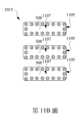
然後方法200繼續到形成層間介電(inter-layer dielectric,ILD)層的方塊212。參照第10A圖、第10B圖、第10C圖和第10D圖的示例,在方塊212的實施方式中,在閘極全環裝置300A和鰭式場效電晶體裝置300B中的每個上形成層間介電層902。根據一些實施方式,第10A圖和第10B圖分別提供閘極全環裝置300A和鰭式場效電晶體裝置300B的等軸測視圖。第10C圖和第10D圖分別提供閘極全環裝置300A和鰭式場效電晶體裝置300B沿著平行於如第10A圖和第10B圖所示的剖面X2-X2'的平面的剖面圖。在一些實施方式中,在形成層間介電層902之前,在閘極全環裝置300A和鰭式場效電晶體裝置300B中的每一個上形成接觸蝕刻停止層(contact etch stop layer,CESL)。在一些示例中,接觸蝕刻停止層包括氮化矽層、氧化矽層、氮氧化矽層和/或所屬技術領域中已知的其它材料。接觸蝕刻停止層可以藉由電漿增強化學氣相沉積(PECVD)製程和/或其他合適的沉積或氧化製程形成。在一些實施方式中,層間介電層902包括諸如正矽酸四乙酯(tetraethylorthosilicate,TEOS)氧化物、未摻雜的矽酸鹽玻璃或摻雜氧化矽的如硼磷矽酸鹽玻璃(borophosphosilicate glass,BPSG)、氟矽酸鹽玻璃(FSG)、磷矽酸鹽玻璃(phosphosilicate glass,PSG)、硼摻雜矽玻璃(boron doped silicon glass,BSG)和/或其它合適的介電材料等。層間介電層902可以藉由PECVD製程或其它合適的沉積技術沉積。在一些實施方式中,在形成層間介電層902之後,每個閘極全環裝置300A和鰭式場效電晶體裝置300B可以經受高熱預算製程以退火層間介電層。The
在一些示例中,在沉積層間介電層(和/或接觸蝕刻停止層或其它介電層)之後,可以執行平坦化製程以暴露閘極全環裝置300A和鰭式場效電晶體裝置300B的閘極堆疊702和閘極堆疊704的頂表面。例如平坦化製程包括CMP製程,移除覆蓋在閘極堆疊702和閘極堆疊704上的層間介電層902(和接觸蝕刻停止層,如果存在)的部分,並使每個閘極全環裝置300A和鰭式場效電晶體裝置300B的頂表面平坦。此外,CMP製程可以移除覆蓋在閘極堆疊702和閘極堆疊704上的硬遮罩層708和硬遮罩層710以露出底層的虛擬閘極的電極層,例如多晶矽電極層。In some examples, after depositing the interlayer dielectric layer (and/or the contact etch stop layer or other dielectric layer), a planarization process can be performed to expose the top surfaces of the
方法200繼續到方塊214,其中虛擬閘極(參見方塊204)被移除,並且如果需要(例如根據需求所製造的閘極全環裝置300A)可執行通道層釋放製程。參照第10A圖、第10B圖、第10C圖、第10D圖、第10E圖和第10F圖的示例,在方塊214的實施方式中,移除每個閘極全環裝置300A和鰭式場效電晶體裝置300B上的虛擬的閘極堆疊702和閘極堆疊704的電極層和介電層,並對閘極全環裝置300A執行通道層釋放製程以釋放半導體通道層(例如磊晶層308)。第10E圖和第10F圖分別提供閘極全環裝置300A和鰭式場效電晶體裝置300B沿著如第10A圖和第10B圖所示的平行於剖面Y2-Y2'的平面的剖面圖。The
在一些實施方式中,每個閘極全環裝置300A和鰭式場效電晶體裝置300B上的虛擬的閘極堆疊702和閘極堆疊704的電極層(例如多晶矽閘極電極)可先藉由適當的蝕刻製程移除。在移除虛擬的電極層之後,執行蝕刻製程以蝕刻每個閘極全環裝置300A和鰭式場效電晶體裝置300B上的虛擬的閘極堆疊702和閘極堆疊704的虛擬的閘極介電層。以另一種方式說明,在方塊214中移除虛擬閘極可以包括從每個閘極全環裝置300A和鰭式場效電晶體裝置300B的閘極堆疊702和閘極堆疊704中移除元件707(其包括虛擬的介電層和電極層)。在一些示例中,蝕刻製程可包括濕蝕刻、乾蝕刻或其組合。In some embodiments, the electrode layer (e.g., polysilicon gate electrode) of the
在從閘極全環裝置300A和鰭式場效電晶體裝置300B上移除虛擬閘極之後,在一些示例和方塊214的實施方式中,對閘極全環裝置300A執行通道釋放製程,其中閘極全環裝置300A的通道區域中的磊晶層306(虛擬層)可以被選擇性地移除(例如使用選擇性蝕刻製程),而磊晶層308(半導體通道層)保持未蝕刻。在實施方式中,所選擇的磊晶層藉由移除閘極全環裝置300A的虛擬閘極所提供的溝槽從鰭602上移除。在一些實施方式中,選擇性的蝕刻製程可包括選擇性的濕蝕刻製程。在一些實施中,選擇性的濕蝕刻包括氨和/或臭氧。僅作為一個例子,選擇性的濕蝕刻製程包括四甲基氫氧化銨(tetra-methyl ammonium hydroxide,TMAH)。在一些實施方式中,選擇性的蝕刻製程可以包括藉由使用CERTAS®氣體化學蝕刻系統(CERTAS® Gas Chemical Etch System)所執行的乾燥、無電漿蝕刻製程,且此系統可從日本東京電子有限公司(Tokyo Electron Limited,Tokyo,Japan)獲得。After removing the dummy gate from the gate-all-around
需要注意的是,由於選擇性地移除磊晶層306(虛擬層),間隙1002形成在閘極全環裝置300A的通道區域中相鄰的半導體通道層(磊晶層308)之間,如第10A圖、第10C圖和第10E圖所示。作為示例,間隙1002可用於暴露磊晶層308的表面,且其上將形成一層或多層閘極結構。例如如下文更詳細地描述,閘極結構的一部分(例如包括具有介面層、高k值介電層和一個或多個金屬電極層的金屬閘極堆疊)將在相鄰的半導體通道層(磊晶層308)之間的間隙1002中形成。在一些實施方式中,在移除虛擬層(磊晶層306)之後,並且在形成閘極結構的部分之前,可以執行片材修剪製程(例如蝕刻製程)以修改半導體通道層(例如磊晶層308)的輪廓以實現所需尺寸和/或所需形狀(例如圓柱形(例如奈米線)、矩形(例如奈米棒)、片狀(例如奈米片)等)的半導體通道層(磊晶層308)。因此在方塊214之後,用於形成閘極全環裝置300A的通道區域的半導體通道層(磊晶層308)的一部分和用於形成鰭式場效電晶體裝置300B的通道區域的磊晶層402的一部分被暴露。It should be noted that due to the selective removal of the epitaxial layer 306 (dummy layer), a
然後方法200繼續進入方塊216,執行第二通道摻雜製程。參照第11A圖和第11B圖,在方塊216的實施方式中,對閘極全環裝置300A執行第二通道摻雜製程。第11A圖和第11B圖提供如第10E圖所示的閘極全環裝置300A的部分1015的放大視圖。在一示例中,磊晶層308(例如半導體通道層)靠近磊晶層308表面(例如靠近將成為通道至閘極介電介面的地方)的一部分可以被有意地摻雜,以使電流路徑(例如在源極和汲極之間)遠離電晶體的通道至閘極介電介面一距離(例如大於約2Å)。The
如第11A圖所示,經原子層沉積的摻雜層1109可以在每個磊晶層308上形成,例如在方塊214中的通道釋放製程之後。經原子層沉積的摻雜層1109可以與上述經原子層沉積的摻雜層509基本上相同。因此經原子層沉積的摻雜層1109可用於沿著每個磊晶層308的表面形成摻雜層1105,類似於摻雜層505。在一些實施方式中,經原子層沉積的摻雜層1109的摻雜劑種類可以包括和與將其引入的電晶體具相同類型(極性)者,或和與將其引入的裝置中的源極/汲極摻類具相同類型(極性)者,如上文所述。雖然摻雜劑種類可以是同一類型(極性),但需要注意的是,摻雜層1105的摻雜劑濃度小於源極/汲極的摻雜劑濃度。作為示例,如果閘極全環裝置300A是N型裝置,則經原子層沉積的摻雜層1109可以包括N型摻雜劑物種(例如如磷、砷、銻的第V欄元素和/或如帶負電的磷離子的帶電負離子)。在另一示例中,如果閘極全環裝置300A是P型裝置,則經原子層沉積的摻雜層1109可以包括P型摻雜劑種類(例如如硼的第III欄列元素和/或如帶正電的硼離子的帶電正離子)。在一些實施中,經原子層沉積的摻雜層1109可以包括用於N型裝置的基於F的層(例如WFx)和用於P型裝置的基於Al的層(例如TiAl)。在經原子層沉積的摻雜層1109之後,可以執行趨入退火以使經原子層沉積的摻雜層1109內的摻雜劑擴散到每個磊晶層308的表面以形成摻雜層1105(例如如第11B圖所示)。在趨入退火之後,在一些實施中,可以使用合適的蝕刻製程(例如濕蝕刻製程、乾蝕刻製程或其組合)移除經原子層沉積的摻雜層1109的任何剩餘部分。在一些實施方式中,由於形成摻雜層1105,閘極全環裝置300A可以類似於埋入式通道電晶體進行工作,其中在閘極全環裝置300A的操作期間,電流主要流經閘極全環裝置300A中源極和汲極之間的每個磊晶層308中的主體部分1107且遠離通道至閘極介電介面。在一些實施中,可以使用電漿摻雜(PLAD)製程來形成摻雜層1105,而不使用經原子層沉積的摻雜層1109。As shown in FIG. 11A , an
方法200接著繼續方塊218,為閘極全環裝置300A和鰭式場效電晶體裝置300B中的每一個形成閘極結構。如下文更詳細地描述,閘極結構可以包括閘極介電質和閘極介電質上形成的金屬閘極。在一些實施方式中,閘極結構可以形成與閘極全環裝置300A中的多個半導體通道(磊晶層308)相關聯的閘極,以及與鰭式場效電晶體裝置300B通道區域中由磊晶層402提供的半導體通道相關聯的閘極。The
參照第12A圖、第12C圖和第12E圖的示例,在方塊218的實施方式中,閘極介電質藉由移除虛擬閘極和通道釋放製程在閘極全環裝置300A的溝槽內形成,參照上述方塊214的描述。根據一些實施方式,第12A圖提供閘極全環裝置300A的等軸測視圖。第12C圖提供閘極全環裝置300A沿著平行於如第10A圖所示的剖面X2-X2'的平面的剖面圖。第12E圖提供閘極全環裝置300A沿著平行於如第10A圖所示的剖面Y2-Y2'的平面的剖面圖。在一些實施方式中,閘極介電質包括介面層(interfacial IL)1102和在介面層上形成的高k值閘極介電層1104。本文使用和描述的高k值的閘極介電質包括具有高介電常數的介電材料,例如大於熱氧化矽(~3.9)。包括介面層1102及在介面層1102上的高k值閘極介電層1104的閘極介電質也形成在藉由移除虛擬閘極而得到的鰭式場效電晶體裝置300B的溝槽中,如第12B圖、第12D圖和第12G圖的示例所示。根據一些實施方式,第12B圖提供鰭式場效電晶體裝置300B的等軸測視圖。第12D圖提供鰭式場效電晶體裝置300B沿著平行於如第10B圖所示的剖面X2-X2'的平面的剖面圖。第12G圖提供鰭式場效電晶體裝置300B沿著平行於如第10B圖所示的剖面Y2-Y2'的平面的剖面圖。Referring to the examples of FIGS. 12A, 12C, and 12E, in an implementation of block 218, a gate dielectric is formed in a trench of a gate all-around
在一些實施方式中,介面層1102可以包括介電材料,例如氧化矽(SiO2)、HfSiO或氮氧化矽(SiON)。介面層可以藉由化學氧化、熱氧化、ALD、CVD和/或其他合適的方法形成。高k值閘極介電層1104可以包括高k值的介電層,例如氧化鉿(HfO2)。可選地,高k值閘極介電層1104可以包括其它高k值的介電質,例如TiO2、HfZrO、Ta2O3、HfSiO4、ZrO2、ZrSiO2、LaO、AlO、ZrO、TiO、Ta2O5、Y2O3、SrTiO3(STO)、BaTiO3(BTO)、BaZrO、HfZrO、HfLaO、HfSiO、LaSiO、AlSiO、HfTaO、HfTiO、(Ba,Sr)TiO3(BST)、Al2O3、Si3N4、氮氧化物(SiON)、其組合或其它合適的材料。高k值閘極介電層1104可以藉由ALD、PVD、CVD、氧化和/或其它合適的方法形成。In some embodiments, the
在不同的示例中,在介面層1102的沉積和/或高k值閘極介電層1104的沉積之後,可以執行沉積後退火(post-deposition anneal,PDA)製程以減少介面阱和氧化物阱,從而降低閃爍雜訊。在一些實施方式中,沉積後退火製程在攝氏約80度至150度的PDA浸泡溫度下在氮氣(N2)環境中執行約40秒至80秒的持續時間。沉積後退火製程可具有填充氧化物空位的效果,從而減少氧化物捕捉中心。In various examples, after deposition of the
在方塊218的進一步實施方式中,在閘極全環裝置300A的閘極介電質和鰭式場效電晶體裝置300B的閘極介電質上形成包括金屬層1202的金屬閘極。金屬層1202可以包括金屬、金屬合金或金屬矽化物。此外,閘極介電質/金屬閘極堆疊的形成可以包括沉積,以形成各種閘極材料、一個或多個襯層;以及包括一個或多個CMP製程,以移除過多的閘極材料並由此使閘極全環裝置300A和鰭式場效電晶體裝置300B的頂表面平坦。在一些示例中,在沉積金屬層1202之後,可以執行任選的金屬化後退火(post-metallization anneal,PMA)製程以進一步減少介面阱和氧化物阱,從而降低閃爍雜訊。In a further implementation of block 218, a metal gate including a
在一些實施方式中,金屬層1202可以包括單層或可選地多層結構,例如具有選定功函數以增強裝置性能的金屬層(功函數金屬層)、襯層、潤濕層(wetting layer)、黏附層、金屬合金或金屬矽化物的各種組合。作為示例,金屬層1202可以包括Ti、Ag、Al、TiAlN、TaC、TaCN、TaSiN、Mn、Zr、TiN、TaN、Ru、Mo、WN、Cu、W、Re、Ir、Co、Ni、其它合適的金屬材料或其組合。在至少一些情況下,金屬層1202可以包括厚的覆蓋層(例如TiN覆蓋層),厚度在約10Å至80Å之間,且形成閘極介電質上,以減少氧吸收到閘極介電質中並減少氧化物缺陷,從而降低閃爍雜訊。在一些示例中,厚的覆蓋層可以包括具有原位矽烷預處理製程(TiN-iSP)的TiN覆蓋層,以在TiN覆蓋層上形成高品質的Si,而不是藉由熱製程而潛在地吸收氧氣。在一些實施方式中,金屬層1202可以藉由ALD、PVD、CVD、電子束蒸發或其它合適的製程形成。此外,金屬層1202可以分別形成用於使用不同金屬層的N型電晶體和P型電晶體。在一些實施方式中,可以執行CMP製程以從金屬層1202上移除過多的金屬,並由此提供金屬層1202基本上平面的頂面。此外,金屬層1202可以提供N型或P型的功函數,以用作閘極全環裝置300A和鰭式場效電晶體裝置300B的閘極,並且在至少一些實施方式中,金屬層1202可以包括多晶矽層。相對於閘極全環裝置300A,閘極結構包括插入每個磊晶層308的部分且各自形成閘極全環裝置300A的通道。In some embodiments, the
需要注意的是,閘極全環裝置300A被圖示為不包括具有在相鄰的磊晶層308之間的閘極結構的部分的側端1111上的內部間隙物層(例如如第12C圖所示)。然而在一些實施中,閘極全環裝置300A可以包括內部間隙物,其中源極/汲極特徵804和源極/汲極特徵806除了接觸半導體通道層(磊晶層308)之外還會與這種內部間隙物接觸。為了揭示如第12C圖所示的示例,相鄰的磊晶層308之間的間距包括合併的IL/HK層(例如介面層1102和高k值閘極介電層1104),而沒有內部間隙物。也如第12C圖的示例所示,半導體通道層(磊晶層308)和合併的IL/HK層延伸至側壁間隙物802下方,且同時相鄰(接觸)源極/汲極特徵804和源極/汲極特徵806。還需注意的是,在一些實施方式中,相鄰的奈米線之間的間距(例如在方向NW-Y上相鄰的磊晶層308之間,如下文所述)可以包括合併的介面層1102,且沒有高k值閘極介電層1104。在這種情況下,高k值閘極介電層1104仍至少設置在奈米線的橫向側(例如在方向NW-X上,下文討論)。此外,在一些示例中,高k值閘極介電層1104的末端或介面層1102的末端可以基本上與側壁間隙物802的外側表面對齊(例如與層間介電層902相鄰的側壁間隙物802的表面),如第12C圖所示。It is noted that the gate-all-around
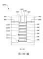
第12F圖提供第12E圖的一部分的放大剖面視圖,其更清楚地說明閘極全環裝置300A的各個方面的結構和尺寸。在一些實施方式中,奈米線的X尺寸(方向NW-X)等於約5奈米至14奈米,而奈米線的Y尺寸(方向NW-Y)等於約5奈米至8奈米。在一些實施中,奈米線的X尺寸(方向NW-X)與奈米線的Y尺寸(方向NW-Y)基本上相同。作為示例,如果奈米線的X尺寸(方向NW-X)大於奈米線的Y尺寸(方向NW-Y),則奈米線結構可以改稱為「奈米片」。在一些實施中,相鄰奈米線(間距NW-space)之間的間距/間隙等於約4奈米至8奈米。需要注意的是,相鄰奈米線之間的間距/間隙(間距NW-space)基本上等於磊晶層306的厚度,磊晶層306先前設置在相鄰奈米線之間,並且如上文所述在方塊214中被移除。在一些實施中,磊晶層306的厚度以及由此產生的相鄰奈米線之間的間距/間隙,可以經選擇以提供相鄰奈米線之間合併的介面層或合併的介面層/高k值閘極介電層的所需厚度,以在相鄰奈米線之間提供完全的間隙填充,且此奈米線也延伸到側壁間隙物802下方,和/或為閘極全環裝置300A提供所需數量的通道區域(例如相鄰奈米線之間的較小間距可以提供額外的磊晶層308,以形成閘極全環裝置300A的通道區域)。在一些實施方式中,介面層1102具有約0.5nm至1.5nm的厚度,而高k值閘極介電層1104具有約1nm至3nm的厚度。FIG. 12F provides an enlarged cross-sectional view of a portion of FIG. 12E that more clearly illustrates the structure and dimensions of various aspects of the gate-all-around
閘極全環裝置300A和鰭式場效電晶體裝置300B中的每個可以經過進一步製程以形成所屬技術領域中已知的各種特徵和區域。例如後續製程可以在基板302上形成接觸開口、接觸金屬以及各種接觸/通孔/線和多層互連特徵(例如金屬層和層間介電質),以配置成連接各種特徵以形成功能電路,並包括一個或多個多閘極裝置。在進一步的示例中,多層互連可以包括垂直互連,例如通孔或觸點,以及水平互連,例如金屬線。各種互連特徵可以採用各種導電材料,包括銅、鎢和/或矽化物。在一例子中,使用鑲嵌和/或雙鑲嵌製程形成與銅相關的多層互連結構。此外,可以在方法200之前、之間和之後執行額外的製程步驟,並且可以根據方法200的一些實施方式替換或移除上述一些製程步驟。Each of the gate
關於本文提供的描述,本揭示內容提供用於降低新進電晶體結構中的雜訊(例如閃爍雜訊)的方法和結構。通常來說,本揭示的實施方式可以藉由改善(降低)介面阱和氧化物阱的密度,以及藉由調節電晶體通道電流路徑(例如電晶體的源極和汲極之間的電流路徑)使電流路徑與電晶體通道至閘極介電介面保持一定距離來有效地降低閃爍雜訊,從而最大限度地減少在通道至閘極介電介面處發生電荷捕捉。在一些實施方式中,阱的減少可以藉由使用沉積後退火製程和/或使用厚的TiN覆蓋層來減少閘極介電質對氧氣的吸收來實現。在一些實施方式中,電流路徑可以藉由摻雜靠近通道至閘極介電介面處的電晶體通道(例如半導體層)來遠離電晶體通道至閘極介電介面。在一示例中,電晶體通道可以使用離子注入製程、擴散摻雜製程、經原子層沉積的摻雜層(ALD deposition of a doped layer)及隨後的趨入退火製程、電漿摻雜(PLAD)製程或使用其他適當的摻雜製程來進行摻雜。特別的是,摻雜製程可用於在靠近通道至閘極介電介面的半導體通道層中引入摻雜劑種類(例如N型摻雜劑種類、P型摻雜劑種類、帶電正離子或帶電負離子),且此摻雜劑種類與其被引入的電晶體類型相同。因此在工作期間,電晶體中的電流將在源極和汲極之間的電晶體的主體部分中流動,並遠離通道至閘極介電介面,從而減少通道到閘極介質介面處載流子的電荷遭到捕捉和相關的閃爍雜訊。所屬技術領域中通常知識者將容易地理解,本文中描述的方法和結構可以應用於各種其它的半導體裝置,以有利地從這些其它的裝置獲得類似的益處,而不脫離本揭示內容的範圍。In connection with the description provided herein, the present disclosure provides methods and structures for reducing noise (e.g., flicker noise) in novel transistor structures. Generally speaking, embodiments of the present disclosure can effectively reduce flicker noise by improving (reducing) the density of interface wells and oxide wells, and by adjusting the transistor channel current path (e.g., the current path between the source and drain of the transistor) to maintain a certain distance from the transistor channel to the gate dielectric interface, thereby minimizing charge trapping at the channel to the gate dielectric interface. In some embodiments, the reduction of wells can be achieved by using a post-deposition annealing process and/or using a thick TiN capping layer to reduce oxygen absorption by the gate dielectric. In some embodiments, the current path can be separated from the transistor channel to the gate dielectric interface by doping the transistor channel (e.g., semiconductor layer) near the channel to the gate dielectric interface. In one example, the transistor channel can be doped using an ion implantation process, a diffusion doping process, an ALD deposition of a doped layer followed by a trend annealing process, a plasma doping (PLAD) process, or using other suitable doping processes. In particular, a doping process can be used to introduce a dopant species (e.g., N-type dopant species, P-type dopant species, positively charged ions, or negatively charged ions) in a semiconductor channel layer near a channel-to-gate dielectric interface, and the dopant species is the same type as the transistor into which it is introduced. Thus, during operation, the current in the transistor will flow in the bulk of the transistor between the source and drain and away from the channel-to-gate dielectric interface, thereby reducing charge trapping of carriers at the channel-to-gate dielectric interface and the associated flicker noise. Those skilled in the art will readily appreciate that the methods and structures described herein may be applied to various other semiconductor devices to advantageously obtain similar benefits from such other devices without departing from the scope of the present disclosure.
因此本揭示內容的一個實施方式描述了製造半導體裝置的方法。方法包括以下操作。提供從基板延伸的第一鰭。形成第一閘極堆疊在第一鰭上。形成第一摻雜層沿著第一鰭的表面及第一閘極堆疊下方,其中第一摻雜層的第一摻雜劑種類與半導體裝置的源極/汲極特徵的第二摻雜劑種類具有相同的極性。在一些實施方式中,第一摻雜層的第一摻雜劑濃度小於源極/汲極特徵的第二摻雜劑濃度。在一些實施方式中,第一摻雜層使半導體裝置的電流路徑遠離通道至閘極介電介面一距離。在一些實施方式中,形成第一摻雜層包括在第一鰭的表面執行離子注入製程,以及其中離子注入製程至少穿透第一閘極堆疊的下部以形成位在第一閘極堆疊下方的第一摻雜層。在一些實施方式中,形成第一摻雜層包括:在形成第一閘極堆疊之前,形成經原子層沉積的摻雜層在第一鰭上;在形成經原子層沉積的摻雜層之後,執行趨入退火以使得經原子層沉積的摻雜層中的多個摻雜劑擴散到第一鰭的表面以形成第一摻雜層;以及在執行趨入退火之後,移除經原子層沉積的摻雜層的剩餘部分。在一些實施方式中,在移除經原子層沉積的摻雜層的剩餘部分之後,第一閘極堆疊形成在第一鰭上。在一些實施方式中,形成第一摻雜層包括在形成第一閘極堆疊之前執行電漿摻雜製程。在一些實施方式中,源極/汲極特徵的第二摻雜劑種類包括N型摻雜劑種類,以及其中第一摻雜層的第一摻雜劑種類包括磷、砷、銻及帶電負離子中的至少一者。在一些實施方式中,源極/汲極特徵的第二摻雜劑種類包括P型摻雜劑種類,以及其中第一摻雜層的第一摻雜劑種類包括硼及帶電正離子中的至少一者。在一些實施方式中,方法更包括:提供從基板延伸的第二鰭,其中第二鰭包括彼此之間具有間隙的複數個半導體通道層;在這些半導體通道層中的每一個的多個表面上形成經原子層沉積的摻雜層;在形成經原子層沉積的摻雜層之後,執行趨入退火以使得經原子層沉積的摻雜層中的多個摻雜劑擴散到這些半導體通道層中的每一個的表面,以沿著這些半導體通道層中的每一個的表面形成第二摻雜層;以及在執行趨入退火之後,移除經原子層沉積的摻雜層的剩餘部分。Thus, one embodiment of the present disclosure describes a method of manufacturing a semiconductor device. The method includes the following operations. A first fin extending from a substrate is provided. A first gate stack is formed on the first fin. A first doping layer is formed along a surface of the first fin and below the first gate stack, wherein a first dopant species of the first doping layer has the same polarity as a second dopant species of a source/drain feature of the semiconductor device. In some embodiments, the first dopant concentration of the first doping layer is less than the second dopant concentration of the source/drain feature. In some embodiments, the first doped layer allows a current path of the semiconductor device to be away from the channel to the gate dielectric surface by a distance. In some embodiments, forming the first doped layer includes performing an ion implantation process on the surface of the first fin, and wherein the ion implantation process at least penetrates the lower portion of the first gate stack to form the first doped layer below the first gate stack. In some embodiments, forming the first doped layer includes: forming an atomic layer deposited doped layer on the first fin before forming the first gate stack; after forming the atomic layer deposited doped layer, performing a run-in anneal to allow a plurality of dopants in the atomic layer deposited doped layer to diffuse to a surface of the first fin to form the first doped layer; and after performing the run-in anneal, removing a remaining portion of the atomic layer deposited doped layer. In some embodiments, after removing the remaining portion of the atomically deposited doping layer, a first gate stack is formed on the first fin. In some embodiments, forming the first doping layer includes performing a plasma doping process before forming the first gate stack. In some embodiments, the second dopant species of the source/drain features includes an N-type dopant species, and wherein the first dopant species of the first doping layer includes at least one of phosphorus, arsenic, antimony, and negatively charged ions. In some embodiments, the second dopant species of the source/drain features includes a P-type dopant species, and wherein the first dopant species of the first doping layer includes at least one of boron and positively charged ions. In some embodiments, the method further includes: providing a second fin extending from the substrate, wherein the second fin includes a plurality of semiconductor channel layers having gaps therebetween; forming an atomically layer deposited doping layer on a plurality of surfaces of each of the semiconductor channel layers; after forming the atomically layer deposited doping layer, performing a run-in annealing to diffuse a plurality of dopants in the atomically layer deposited doping layer to a surface of each of the semiconductor channel layers to form a second doping layer along a surface of each of the semiconductor channel layers; and after performing the run-in annealing, removing a remaining portion of the atomically layer deposited doping layer.
在另一個實施方式中,討論的是製造多閘極半導體裝置的方法。方法包括以下操作。提供從基板延伸的鰭,其中鰭包括具有複數個第二磊晶層插置其間的複數個第一磊晶層。選擇性地移除第二磊晶層以在這些第一磊晶層中相鄰的多者之間形成多個間隙並暴露出第一磊晶層的多個表面。在第一磊晶層暴露的表面上形成第一摻雜層。執行趨入退火以使得第一摻雜層中的多個摻雜劑擴散到第一磊晶層的表面,以沿著第一磊晶層的表面形成第二摻雜層。在執行趨入退火之後,移除第一摻雜層的剩餘部分。在一些實施方式中,方法更包括形成閘極結構,其中閘極結構的多個部分插置於第一磊晶層中。在一些實施方式中,第二摻雜層的摻雜劑種類與多閘極半導體裝置的源極/汲極特徵具有相同的極性。在一些實施方式中,第二摻雜層的第一摻雜劑濃度小於源極/汲極特徵的第二摻雜劑濃度。在一些實施方式中,在多閘極半導體裝置的操作期間,第二摻雜層使電流在遠離通道至閘極介電介面一距離的第一磊晶層的主體部分中流動。在一些實施方式中,多閘極半導體裝置包括N型裝置,以及其中第二摻雜層的摻雜劑種類包括磷、砷、銻及帶電負離子中的至少一者。在一些實施方式中,多閘極半導體裝置包括P型裝置,以及其中第二摻雜層的摻雜劑種類包括硼及帶電正離子中的至少一者。In another embodiment, a method for manufacturing a multi-gate semiconductor device is discussed. The method includes the following operations. A fin extending from a substrate is provided, wherein the fin includes a plurality of first epitaxial layers having a plurality of second epitaxial layers interposed therebetween. The second epitaxial layers are selectively removed to form a plurality of gaps between adjacent ones of the first epitaxial layers and to expose a plurality of surfaces of the first epitaxial layers. A first doped layer is formed on the exposed surface of the first epitaxial layer. A run-in anneal is performed to diffuse a plurality of dopants in the first doped layer to the surface of the first epitaxial layer to form a second doped layer along the surface of the first epitaxial layer. After performing the run-in anneal, the remaining portion of the first doping layer is removed. In some embodiments, the method further includes forming a gate structure, wherein multiple portions of the gate structure are inserted into the first epitaxial layer. In some embodiments, the dopant type of the second doping layer has the same polarity as the source/drain features of the multi-gate semiconductor device. In some embodiments, the first dopant concentration of the second doping layer is less than the second dopant concentration of the source/drain features. In some embodiments, during operation of the multi-gate semiconductor device, the second doping layer causes current to flow in a bulk portion of the first epitaxial layer at a distance from the channel to the gate dielectric plane. In some embodiments, the multi-gate semiconductor device includes an N-type device, and wherein the dopant species of the second doping layer includes at least one of phosphorus, arsenic, antimony, and negatively charged ions. In some embodiments, the multi-gate semiconductor device includes a P-type device, and wherein the dopant species of the second doping layer includes at least one of boron and positively charged ions.
在又一個實施方式中,討論的是多閘極半導體裝置。多閘極半導體裝置包括包括複數個矽磊晶層的第一鰭、在第一鰭的通道區域上的第一閘極結構,以及與第一鰭的通道區域相鄰的第一磊晶源極/汲極特徵。矽磊晶層中的每一個包括沿著矽磊晶層的表面的第一摻雜層,以及第一摻雜層具有第一極性類型及第一摻雜劑濃度。第一閘極結構的一部分設置在矽磊晶層的相鄰多層之間。第一磊晶源極/汲極特徵具有與第一極性類型相同的第二極性類型,以及第一磊晶源極/汲極特徵具有大於第一摻雜劑濃度的第二摻雜劑濃度。在一些實施方式中,多閘極半導體裝置更包括包括矽鍺層的第二鰭、在第二鰭的通道區域上的第二閘極結構,以及與第二鰭的通道區域相鄰的第二磊晶源極/汲極特徵。矽鍺層包括沿著矽鍺層的表面的第二摻雜層,以及第二摻雜層具有第三極性類型及第三摻雜劑濃度。第二磊晶源極/汲極特徵具有與第三極性類型相同的第四極性類型,以及第二磊晶源極/汲極特徵具有大於第三摻雜劑濃度的第四摻雜劑濃度。在一些實施方式中,閘極全環裝置包括第一鰭,以及鰭式場效電晶體裝置包括第二鰭。In yet another embodiment, a multi-gate semiconductor device is discussed. The multi-gate semiconductor device includes a first fin including a plurality of epitaxial silicon layers, a first gate structure on a channel region of the first fin, and a first epitaxial source/drain feature adjacent to the channel region of the first fin. Each of the epitaxial silicon layers includes a first doped layer along a surface of the epitaxial silicon layer, and the first doped layer has a first polarity type and a first dopant concentration. A portion of the first gate structure is disposed between adjacent layers of the epitaxial silicon layers. The first epitaxial source/drain feature has a second polarity type that is the same as the first polarity type, and the first epitaxial source/drain feature has a second dopant concentration that is greater than the first dopant concentration. In some embodiments, the multi-gate semiconductor device further includes a second fin including a silicon germanium layer, a second gate structure on a channel region of the second fin, and a second epitaxial source/drain feature adjacent to the channel region of the second fin. The silicon germanium layer includes a second dopant layer along a surface of the silicon germanium layer, and the second dopant layer has a third polarity type and a third dopant concentration. The second epitaxial source/drain feature has a fourth polarity type that is the same as the third polarity type, and the second epitaxial source/drain feature has a fourth dopant concentration that is greater than the third dopant concentration. In some embodiments, the gate-all-around device includes a first fin, and the fin field effect transistor device includes a second fin.
前述概述幾個實施方式的特徵,以便所屬技術領域中通常知識者可以更好地理解本揭示內容的各個方面。所屬技術領域中通常知識者應當理解,他們可以容易地使用本揭示內容作為設計或修改其它製程和結構的基礎,以執行相同的目的和/或實現本文介紹的實施方式的相同優點。所屬技術領域中通常知識者還應當認識到,這種等效結構並不背離本揭示內容的精神和範圍,並且它們可以在不脫離本揭示內容的精神和範圍的情況下執行本文的各種更改、替換和修改。The foregoing summarizes the features of several implementations so that those skilled in the art can better understand the various aspects of this disclosure. Those skilled in the art should understand that they can easily use this disclosure as a basis for designing or modifying other processes and structures to perform the same purpose and/or achieve the same advantages of the implementations described herein. Those skilled in the art should also recognize that such equivalent structures do not depart from the spirit and scope of this disclosure, and that they can perform various changes, substitutions, and modifications of this disclosure without departing from the spirit and scope of this disclosure.
100:電晶體100: Transistor
102:基板102: Substrate
104:閘極堆疊104: Gate stack
106:閘極介電質106: Gate dielectric
108:閘極電極108: Gate electrode
110:源極區域110: Source region
112:汲極區域112: Drain area
114:通道區域114: Channel area
L:通道長度L: Channel length
W:通道寬度W: Channel width
Claims (10)
Translated fromChineseApplications Claiming Priority (2)
| Application Number | Priority Date | Filing Date | Title |
|---|---|---|---|
| US18/348,780US20250015167A1 (en) | 2023-07-07 | 2023-07-07 | Multi-gate device and related methods |
| US18/348,780 | 2023-07-07 |
Publications (2)
| Publication Number | Publication Date |
|---|---|
| TWI863785Btrue TWI863785B (en) | 2024-11-21 |
| TW202503905A TW202503905A (en) | 2025-01-16 |
Family
ID=93232081
Family Applications (1)
| Application Number | Title | Priority Date | Filing Date |
|---|---|---|---|
| TW112151435ATWI863785B (en) | 2023-07-07 | 2023-12-28 | Method of fabricating semiconductor device, multi-gate semiconductor device and method of fabricating the same |
Country Status (3)
| Country | Link |
|---|---|
| US (1) | US20250015167A1 (en) |
| CN (1) | CN118888444A (en) |
| TW (1) | TWI863785B (en) |
Citations (3)
| Publication number | Priority date | Publication date | Assignee | Title |
|---|---|---|---|---|
| US10332803B1 (en)* | 2018-05-08 | 2019-06-25 | Globalfoundaries Inc. | Hybrid gate-all-around (GAA) field effect transistor (FET) structure and method of forming |
| US20200168742A1 (en)* | 2018-11-27 | 2020-05-28 | Taiwan Semiconductor Manufacturing Co., Ltd. | Gate-All-Around Structure and Methods of Forming the Same |
| US20200411656A1 (en)* | 2016-04-25 | 2020-12-31 | Applied Materials, Inc. | Horizontal gate all around device nanowire air gap spacer formation |
Family Cites Families (4)
| Publication number | Priority date | Publication date | Assignee | Title |
|---|---|---|---|---|
| US11600528B2 (en)* | 2020-05-28 | 2023-03-07 | Taiwan Semiconductor Manufacturing Co., Ltd. | Semiconductor structure and method for forming the same |
| US11862638B2 (en)* | 2020-08-14 | 2024-01-02 | Taiwan Semiconductor Manufacturing Co., Ltd. | Semiconductor device and method |
| US11600533B2 (en)* | 2020-09-18 | 2023-03-07 | Taiwan Semiconductor Manufacturing Company, Ltd. | Semiconductor device fabrication methods and structures thereof |
| US12424443B2 (en)* | 2021-12-08 | 2025-09-23 | Texas Instruments Incorporated | Fin field-effect transistor semiconductor device and method of forming the same |
- 2023
- 2023-07-07USUS18/348,780patent/US20250015167A1/enactivePending
- 2023-12-28TWTW112151435Apatent/TWI863785B/enactive
- 2024
- 2024-02-20CNCN202410189506.5Apatent/CN118888444A/enactivePending
Patent Citations (3)
| Publication number | Priority date | Publication date | Assignee | Title |
|---|---|---|---|---|
| US20200411656A1 (en)* | 2016-04-25 | 2020-12-31 | Applied Materials, Inc. | Horizontal gate all around device nanowire air gap spacer formation |
| US10332803B1 (en)* | 2018-05-08 | 2019-06-25 | Globalfoundaries Inc. | Hybrid gate-all-around (GAA) field effect transistor (FET) structure and method of forming |
| US20200168742A1 (en)* | 2018-11-27 | 2020-05-28 | Taiwan Semiconductor Manufacturing Co., Ltd. | Gate-All-Around Structure and Methods of Forming the Same |
Also Published As
| Publication number | Publication date |
|---|---|
| CN118888444A (en) | 2024-11-01 |
| US20250015167A1 (en) | 2025-01-09 |
| TW202503905A (en) | 2025-01-16 |
Similar Documents
| Publication | Publication Date | Title |
|---|---|---|
| US11942548B2 (en) | Multi-gate device and method of fabrication thereof | |
| US10943925B2 (en) | Method of forming FinFET channel and structures thereof | |
| US11355611B2 (en) | Multi-gate device and method of fabrication thereof | |
| US11972981B2 (en) | FinFET channel on oxide structures and related methods | |
| US10790280B2 (en) | Multi-gate device and method of fabrication thereof | |
| US11211295B2 (en) | FinFET doping methods and structures thereof | |
| US9704755B2 (en) | Multi-gate device structure including a fin-embedded isolation region and methods thereof | |
| US9899269B2 (en) | Multi-gate device and method of fabrication thereof | |
| US12191307B2 (en) | Multi-gate device and related methods | |
| US20150380558A1 (en) | Finfet thermal protection methods and related structures | |
| TWI863785B (en) | Method of fabricating semiconductor device, multi-gate semiconductor device and method of fabricating the same |