TWI861536B - Semiconductor device - Google Patents
Semiconductor deviceDownload PDFInfo
- Publication number
- TWI861536B TWI861536BTW111128418ATW111128418ATWI861536BTW I861536 BTWI861536 BTW I861536BTW 111128418 ATW111128418 ATW 111128418ATW 111128418 ATW111128418 ATW 111128418ATW I861536 BTWI861536 BTW I861536B
- Authority
- TW
- Taiwan
- Prior art keywords
- layer
- oxide semiconductor
- electrode layer
- oxide
- film
- Prior art date
Links
Images


Classifications
- H—ELECTRICITY
- H10—SEMICONDUCTOR DEVICES; ELECTRIC SOLID-STATE DEVICES NOT OTHERWISE PROVIDED FOR
- H10D—INORGANIC ELECTRIC SEMICONDUCTOR DEVICES
- H10D30/00—Field-effect transistors [FET]
- H10D30/60—Insulated-gate field-effect transistors [IGFET]
- H10D30/67—Thin-film transistors [TFT]
- H10D30/674—Thin-film transistors [TFT] characterised by the active materials
- H10D30/6755—Oxide semiconductors, e.g. zinc oxide, copper aluminium oxide or cadmium stannate
- H—ELECTRICITY
- H01—ELECTRIC ELEMENTS
- H01L—SEMICONDUCTOR DEVICES NOT COVERED BY CLASS H10
- H01L21/00—Processes or apparatus adapted for the manufacture or treatment of semiconductor or solid state devices or of parts thereof
- H01L21/02—Manufacture or treatment of semiconductor devices or of parts thereof
- H01L21/02104—Forming layers
- H01L21/02365—Forming inorganic semiconducting materials on a substrate
- H01L21/02518—Deposited layers
- H01L21/02521—Materials
- H01L21/02551—Group 12/16 materials
- H01L21/02554—Oxides
- H—ELECTRICITY
- H01—ELECTRIC ELEMENTS
- H01L—SEMICONDUCTOR DEVICES NOT COVERED BY CLASS H10
- H01L21/00—Processes or apparatus adapted for the manufacture or treatment of semiconductor or solid state devices or of parts thereof
- H01L21/02—Manufacture or treatment of semiconductor devices or of parts thereof
- H01L21/02104—Forming layers
- H01L21/02365—Forming inorganic semiconducting materials on a substrate
- H01L21/02518—Deposited layers
- H01L21/02521—Materials
- H01L21/02565—Oxide semiconducting materials not being Group 12/16 materials, e.g. ternary compounds
- H—ELECTRICITY
- H10—SEMICONDUCTOR DEVICES; ELECTRIC SOLID-STATE DEVICES NOT OTHERWISE PROVIDED FOR
- H10D—INORGANIC ELECTRIC SEMICONDUCTOR DEVICES
- H10D30/00—Field-effect transistors [FET]
- H10D30/60—Insulated-gate field-effect transistors [IGFET]
- H10D30/67—Thin-film transistors [TFT]
- H10D30/6704—Thin-film transistors [TFT] having supplementary regions or layers in the thin films or in the insulated bulk substrates for controlling properties of the device
- H10D30/6713—Thin-film transistors [TFT] having supplementary regions or layers in the thin films or in the insulated bulk substrates for controlling properties of the device characterised by the properties of the source or drain regions, e.g. compositions or sectional shapes
- H—ELECTRICITY
- H10—SEMICONDUCTOR DEVICES; ELECTRIC SOLID-STATE DEVICES NOT OTHERWISE PROVIDED FOR
- H10D—INORGANIC ELECTRIC SEMICONDUCTOR DEVICES
- H10D30/00—Field-effect transistors [FET]
- H10D30/60—Insulated-gate field-effect transistors [IGFET]
- H10D30/67—Thin-film transistors [TFT]
- H10D30/6729—Thin-film transistors [TFT] characterised by the electrodes
- H10D30/673—Thin-film transistors [TFT] characterised by the electrodes characterised by the shapes, relative sizes or dispositions of the gate electrodes
- H10D30/6733—Multi-gate TFTs
- H—ELECTRICITY
- H10—SEMICONDUCTOR DEVICES; ELECTRIC SOLID-STATE DEVICES NOT OTHERWISE PROVIDED FOR
- H10D—INORGANIC ELECTRIC SEMICONDUCTOR DEVICES
- H10D30/00—Field-effect transistors [FET]
- H10D30/60—Insulated-gate field-effect transistors [IGFET]
- H10D30/67—Thin-film transistors [TFT]
- H10D30/6758—Thin-film transistors [TFT] characterised by the insulating substrates
- H—ELECTRICITY
- H10—SEMICONDUCTOR DEVICES; ELECTRIC SOLID-STATE DEVICES NOT OTHERWISE PROVIDED FOR
- H10D—INORGANIC ELECTRIC SEMICONDUCTOR DEVICES
- H10D86/00—Integrated devices formed in or on insulating or conducting substrates, e.g. formed in silicon-on-insulator [SOI] substrates or on stainless steel or glass substrates
- H10D86/40—Integrated devices formed in or on insulating or conducting substrates, e.g. formed in silicon-on-insulator [SOI] substrates or on stainless steel or glass substrates characterised by multiple TFTs
- H10D86/421—Integrated devices formed in or on insulating or conducting substrates, e.g. formed in silicon-on-insulator [SOI] substrates or on stainless steel or glass substrates characterised by multiple TFTs having a particular composition, shape or crystalline structure of the active layer
- H10D86/423—Integrated devices formed in or on insulating or conducting substrates, e.g. formed in silicon-on-insulator [SOI] substrates or on stainless steel or glass substrates characterised by multiple TFTs having a particular composition, shape or crystalline structure of the active layer comprising semiconductor materials not belonging to the Group IV, e.g. InGaZnO
- H—ELECTRICITY
- H10—SEMICONDUCTOR DEVICES; ELECTRIC SOLID-STATE DEVICES NOT OTHERWISE PROVIDED FOR
- H10D—INORGANIC ELECTRIC SEMICONDUCTOR DEVICES
- H10D86/00—Integrated devices formed in or on insulating or conducting substrates, e.g. formed in silicon-on-insulator [SOI] substrates or on stainless steel or glass substrates
- H10D86/40—Integrated devices formed in or on insulating or conducting substrates, e.g. formed in silicon-on-insulator [SOI] substrates or on stainless steel or glass substrates characterised by multiple TFTs
- H10D86/441—Interconnections, e.g. scanning lines
- H—ELECTRICITY
- H10—SEMICONDUCTOR DEVICES; ELECTRIC SOLID-STATE DEVICES NOT OTHERWISE PROVIDED FOR
- H10D—INORGANIC ELECTRIC SEMICONDUCTOR DEVICES
- H10D86/00—Integrated devices formed in or on insulating or conducting substrates, e.g. formed in silicon-on-insulator [SOI] substrates or on stainless steel or glass substrates
- H10D86/40—Integrated devices formed in or on insulating or conducting substrates, e.g. formed in silicon-on-insulator [SOI] substrates or on stainless steel or glass substrates characterised by multiple TFTs
- H10D86/451—Integrated devices formed in or on insulating or conducting substrates, e.g. formed in silicon-on-insulator [SOI] substrates or on stainless steel or glass substrates characterised by multiple TFTs characterised by the compositions or shapes of the interlayer dielectrics
- H—ELECTRICITY
- H10—SEMICONDUCTOR DEVICES; ELECTRIC SOLID-STATE DEVICES NOT OTHERWISE PROVIDED FOR
- H10D—INORGANIC ELECTRIC SEMICONDUCTOR DEVICES
- H10D86/00—Integrated devices formed in or on insulating or conducting substrates, e.g. formed in silicon-on-insulator [SOI] substrates or on stainless steel or glass substrates
- H10D86/40—Integrated devices formed in or on insulating or conducting substrates, e.g. formed in silicon-on-insulator [SOI] substrates or on stainless steel or glass substrates characterised by multiple TFTs
- H10D86/481—Integrated devices formed in or on insulating or conducting substrates, e.g. formed in silicon-on-insulator [SOI] substrates or on stainless steel or glass substrates characterised by multiple TFTs integrated with passive devices, e.g. auxiliary capacitors
- H—ELECTRICITY
- H10—SEMICONDUCTOR DEVICES; ELECTRIC SOLID-STATE DEVICES NOT OTHERWISE PROVIDED FOR
- H10D—INORGANIC ELECTRIC SEMICONDUCTOR DEVICES
- H10D86/00—Integrated devices formed in or on insulating or conducting substrates, e.g. formed in silicon-on-insulator [SOI] substrates or on stainless steel or glass substrates
- H10D86/40—Integrated devices formed in or on insulating or conducting substrates, e.g. formed in silicon-on-insulator [SOI] substrates or on stainless steel or glass substrates characterised by multiple TFTs
- H10D86/60—Integrated devices formed in or on insulating or conducting substrates, e.g. formed in silicon-on-insulator [SOI] substrates or on stainless steel or glass substrates characterised by multiple TFTs wherein the TFTs are in active matrices
- H—ELECTRICITY
- H10—SEMICONDUCTOR DEVICES; ELECTRIC SOLID-STATE DEVICES NOT OTHERWISE PROVIDED FOR
- H10D—INORGANIC ELECTRIC SEMICONDUCTOR DEVICES
- H10D99/00—Subject matter not provided for in other groups of this subclass
- H—ELECTRICITY
- H10—SEMICONDUCTOR DEVICES; ELECTRIC SOLID-STATE DEVICES NOT OTHERWISE PROVIDED FOR
- H10H—INORGANIC LIGHT-EMITTING SEMICONDUCTOR DEVICES HAVING POTENTIAL BARRIERS
- H10H20/00—Individual inorganic light-emitting semiconductor devices having potential barriers, e.g. light-emitting diodes [LED]
- H10H20/80—Constructional details
- H10H20/83—Electrodes
- H10H20/832—Electrodes characterised by their material
- H10H20/833—Transparent materials
- H—ELECTRICITY
- H01—ELECTRIC ELEMENTS
- H01L—SEMICONDUCTOR DEVICES NOT COVERED BY CLASS H10
- H01L2924/00—Indexing scheme for arrangements or methods for connecting or disconnecting semiconductor or solid-state bodies as covered by H01L24/00
- H01L2924/0001—Technical content checked by a classifier
- H01L2924/0002—Not covered by any one of groups H01L24/00, H01L24/00 and H01L2224/00
Landscapes
- Engineering & Computer Science (AREA)
- Physics & Mathematics (AREA)
- Condensed Matter Physics & Semiconductors (AREA)
- General Physics & Mathematics (AREA)
- Manufacturing & Machinery (AREA)
- Computer Hardware Design (AREA)
- Microelectronics & Electronic Packaging (AREA)
- Power Engineering (AREA)
- Thin Film Transistor (AREA)
- Liquid Crystal (AREA)
- Devices For Indicating Variable Information By Combining Individual Elements (AREA)
- Electroluminescent Light Sources (AREA)
- Electrodes Of Semiconductors (AREA)
- Metal-Oxide And Bipolar Metal-Oxide Semiconductor Integrated Circuits (AREA)
- Shift Register Type Memory (AREA)
- Bipolar Transistors (AREA)
Abstract
Description
Translated fromChinese本發明係相關於具有使用薄膜電晶體(下面稱作TFT)所形成的電路之半導體裝置及其製造方法。例如,本發明係相關於以液晶顯示面板為代表之電光裝置,或具有含有機發光元件作為組件的發光顯示裝置之電子裝置。The present invention relates to a semiconductor device having a circuit formed using a thin film transistor (hereinafter referred to as TFT) and a manufacturing method thereof. For example, the present invention relates to an electro-optical device represented by a liquid crystal display panel, or an electronic device having a light-emitting display device having an organic light-emitting element as a component.
需注意的是,在此說明書中,半導體裝置意指可藉由利用半導體特性來運作之所有裝置。電光裝置、半導體電路、和電子器具都是半導體裝置。Please note that in this manual, semiconductor devices refer to all devices that can operate by utilizing the characteristics of semiconductors. Electro-optical devices, semiconductor circuits, and electronic equipment are all semiconductor devices.
需注意的是,作為設置用於電光元件之透明電極的金屬輔助配線之方法,已知金屬輔助配線被設置,以與透明電極的上表面或透明電極的下表面重疊,以及電連接到透明電極之方法(例如,見專利文件1)。It should be noted that as a method of setting a metal auxiliary wiring for a transparent electrode for an electro-optical element, a method of setting the metal auxiliary wiring to overlap with the upper surface of the transparent electrode or the lower surface of the transparent electrode and electrically connecting to the transparent electrode is known (for example, see Patent Document 1).
已知設置用於主動矩陣式基板的額外電容器電極係由ITO、SnO2等具有光透射特性之導電膜所形成,以及由金屬膜所形成之輔助配線係設置成與額外電容器電極接觸,以降低額外電容器電極的電阻之結構(見專利文件2)。It is known that an additional capacitor electrode for an active matrix substrate is formed of a conductive film having light-transmitting properties such as ITO andSnO2 , and an auxiliary wiring formed of a metal film is arranged to contact the additional capacitor electrode to reduce the resistance of the additional capacitor electrode (see patent document 2).
需注意的是,已知作為使用非晶氧化物半導體膜所形成的場效電晶體之閘極電極、源極電極、及汲極電極的每一個,可使用銦錫氧化物(ITO)、銦鋅氧化物、ZnO、SnO2等透明電極,Al(鋁)、Ag(銀)、Cr(鉻)、Ni(鎳)、Mo(鉬)、Au(金)、Ti(鈦)、Ta(鉭)等的金屬電極,含有上述元素的任一個之合金的金屬電極;而且,藉由堆疊兩或更多個這些層,可降低接觸電阻,或者可提高介面強度(例如,見專利文件3)。It should be noted that each of the gate electrode, source electrode, and drain electrode of a field effect transistor formed using an amorphous oxide semiconductor film is known to use a transparent electrode such as indium tin oxide (ITO), indium zinc oxide, ZnO,SnO2 , a metal electrode such as Al (aluminum), Ag (silver), Cr (chromium), Ni (nickel), Mo (molybdenum), Au (gold), Ti (titanium), Ta (tantalum), or a metal electrode containing an alloy of any of the above elements; and by stacking two or more of these layers, the contact resistance can be reduced, or the interface strength can be increased (for example, see patent document 3).
需注意的是,已知作為使用非晶氧化物半導體所形成的電晶體之源極電極、汲極電極、閘極電極、及輔助電容器電極的每一個之材料,可使用諸如銦(In)、鋁(Al)、金(Au)、或銀(Ag)等金屬,諸如氧化銦(In2O3)、氧化錫(SnO2)、氧化鋅(ZnO)、氧化鎘(CdO)、鎘銦氧化物(CdIn2O4)、鎘錫氧化物(Cd2SnO4)、或鋅錫氧化物(Zn2SnO4)等氧化物材料;及相同材料或不同材料可被用於閘極電極、源極電極、及汲極電極(例如,見專利文件4及5)。It should be noted that as a material for each of the source electrode, drain electrode, gate electrode, and auxiliary capacitor electrode of a transistor formed using an amorphous oxide semiconductor, metals such as indium (In), aluminum (Al), gold (Au), or silver (Ag), indium oxide (In2 O3 ), tin oxide (SnO2 ), zinc oxide (ZnO), cadmium oxide (CdO), cadmium indium oxide (CdIn2 O4 ), cadmium tin oxide (Cd2 SnO4 ), or zinc tin oxide (Zn2 SnO4 ) and the same material or different materials can be used for the gate electrode, the source electrode, and the drain electrode (for example, see
[參考文件][Reference Documents]
[參考文件1]日本已出版專利申請案號H02-82221[Reference document 1] Japanese published patent application number H02-82221
[參考文件2]日本已出版專利申請案號H02-310536[Reference Document 2] Japanese published patent application number H02-310536
[參考文件3]日本已出版專利申請案號2008-243928[Reference Document 3] Japanese published patent application number 2008-243928
[參考文件4]日本已出版專利申請案號2007-109918[Reference Document 4] Japanese published patent application number 2007-109918
[參考文件5]日本已出版專利申請案號2007-115807[Reference document 5] Japanese published patent application number 2007-115807
然而,因為具有光透射特性的導電膜僅被用於使用氧化物半導體之習知顯示面板中的電極材料,所以無法提高孔徑比。此外,當使用金屬氧化物製造顯示裝置時,無法將其可靠性列入考量。However, since conductive films having light-transmitting properties are only used as electrode materials in conventional display panels using oxide semiconductors, the aperture ratio cannot be increased. In addition, when a display device is manufactured using metal oxide, its reliability cannot be taken into consideration.
鑑於上述,本發明的一實施例之目的係用以提高使用金屬氧化物所形成之顯示裝置的孔徑比和可靠性。In view of the above, the purpose of one embodiment of the present invention is to improve the aperture ratio and reliability of a display device formed using metal oxide.
在具有使用氧化物半導體膜形成包括通道形成區的半導體層之薄膜電晶體的半導體裝置之製造方法中,執行用以降低是雜質的濕氣等以及用以提高氧化物半導體膜的純淨之熱處理(用於脫水作用或除氫作用的熱處理)。另外,諸如不僅存在於氧化物半導體膜而且亦存在於閘極絕緣層,氧化物半導體膜和上方的膜之間和與之接觸,以及在氧化物半導體膜和下方的膜之間和與之接觸的介面之濕氣等雜質被降低。In a method for manufacturing a semiconductor device having a thin film transistor in which a semiconductor layer including a channel formation region is formed using an oxide semiconductor film, heat treatment (heat treatment for dehydration or dehydrogenation) is performed to reduce moisture and the like which are impurities and to improve the purity of the oxide semiconductor film. In addition, moisture and other impurities which exist not only in the oxide semiconductor film but also in the gate insulating layer, between the oxide semiconductor film and the film above and in contact with it, and between the oxide semiconductor film and the film below and in contact with it are reduced.
此說明書所揭示之本發明的一實施例為半導體裝置的製造方法,其包括以下步驟:將包括金屬氧化物的閘極電極層形成於具有絕緣表面之基板上;將閘極絕緣層形成於閘極電極層上;將氧化物半導體層形成於閘極絕緣層上;將氧化物半導體層脫水或除氫;將源極電極層和汲極電極層形成於脫水或除氫的氧化物半導體層上;將與氧化物半導體層的部分接觸保護絕緣層形成於閘極絕緣層、氧化物半導體層、源極電極層、和汲極電極層上;及將包括金屬氧化物之像素電極層形成在保護絕緣層上。One embodiment of the present invention disclosed in this specification is a method for manufacturing a semiconductor device, which includes the following steps: forming a gate electrode layer including a metal oxide on a substrate having an insulating surface; forming a gate insulating layer on the gate electrode layer; forming an oxide semiconductor layer on the gate insulating layer; dehydrating or drying the oxide semiconductor layer; dehydrogenation; forming a source electrode layer and a drain electrode layer on the dehydrated or dehydrogenated oxide semiconductor layer; forming a protective insulating layer that partially contacts the oxide semiconductor layer on the gate insulating layer, the oxide semiconductor layer, the source electrode layer, and the drain electrode layer; and forming a pixel electrode layer including a metal oxide on the protective insulating layer.
就脫水作用或除氫作用而言,在大於或等於350℃的溫度中或者大於或等於400℃較佳且低於基板的應變點的溫度中,在氧氛圍中,在諸如氮或稀有氣體(氬、氦等)等鈍氣大氣中,或減壓下執行熱處理,藉以降低含在氧化物半導體層中諸如濕氣等雜質。For dehydration or dehydrogenation, heat treatment is performed at a temperature greater than or equal to 350°C or preferably greater than or equal to 400°C and lower than the strain point of the substrate in an oxygen atmosphere, in a passive gas atmosphere such as nitrogen or a rare gas (argon, helium, etc.), or under reduced pressure to reduce impurities such as moisture contained in the oxide semiconductor layer.
以當在溫度增加到450℃的同時以熱去吸附光譜學(TDS)測量脫水或除氫的氧化物半導體層時未偵測到水的兩峰值之約300℃的至少一峰值之熱處理的條件來實施氧化物半導體的脫水作用或除氫作用。因此,甚至當使用脫水或除氫的氧化物半導體層之薄膜電晶體經過溫度如450℃一般高的之TDS時,未偵測到約300℃的水之至少一峰值。Dehydration or dehydrogenation of an oxide semiconductor is performed under heat treatment conditions such that at least one of the two peaks of water at about 300°C is not detected when the dehydrated or dehydrogenated oxide semiconductor layer is measured by thermal desorption spectroscopy (TDS) while the temperature is increased to 450°C. Therefore, even when a thin film transistor using a dehydrated or dehydrogenated oxide semiconductor layer is subjected to TDS at a temperature as high as 450°C, at least one peak of water at about 300°C is not detected.
然後,從氧化物半導體層被脫水或除氫的加熱溫度T至足夠低到防止水再次進來的溫度來執行慢速冷卻,尤其是至低於加熱溫度T之大於100℃的溫度,或者至低於或等於100℃的溫度更好。Then, slow cooling is performed from the heating temperatureT at which the oxide semiconductor layer is dehydrated or dehydrogenated to a temperature low enough to prevent water from entering again, particularly to a temperature greater than 100°C lower than the heating temperatureT , or more preferably to a temperature lower than or equal to 100°C.
加熱溫度T被減少之氣體大氣可轉換到不同於溫度被增加至加熱溫度T者的氣體大氣。The gas atmosphere whose heating temperatureT is reduced may be converted into a gas atmosphere whose temperature is different from that of the gas atmosphere whose temperature is increased to the heating temperatureT.
藉由使用藉由以用於脫水作用或除氫作用之熱處理來降低含在膜中的濕氣,然後在未含濕氣的大氣中(低於或等於-40℃或者低於或等於-60℃較佳的露點溫度)經過慢速冷卻(或冷卻)所形成之氧化物半導體膜,提高薄膜電晶體的電特性,和實現具有大量生產和高性能的薄膜電晶體。By using heat treatment for dehydration or dehydrogenation to reduce the moisture contained in the film, and then slowly cooling (or cooling) the oxide semiconductor film in a non-humidified atmosphere (less than or equal to -40°C or less than or equal to -60°C preferably dew point temperature), the electrical characteristics of the thin film transistor are improved, and a thin film transistor with mass production and high performance is realized.
在此說明書中,在氧氛圍中,在諸如氮或稀有氣體(氬、氦等)等鈍氣大氣中,或減壓下的熱處理被稱作用於脫水作用或除氫作用之熱處理。為了方便,此說明書中的脫水作用或除氫作用不僅意指藉由熱處理去除H2,亦藉由熱處理去除H、OH等。In this specification, heat treatment in an oxygen atmosphere, in a dull atmosphere such as nitrogen or a rare gas (argon, helium, etc.), or under reduced pressure is referred to as heat treatment for dehydration or dehydrogenation. For convenience, dehydration or dehydrogenation in this specification means not only removal of H2 by heat treatment, but also removal of H, OH, etc. by heat treatment.
在諸如氮或稀有氣體(氬、氦等)等鈍氣大氣中,或者在減壓下執行熱處理的例子中,可說是:藉由熱處理將已經是i型的氧化物半導體層變成缺氧型層並且具有低電阻,即、變成n型(諸如n-或n+等);然後,藉由形成與氧化物半導體層接觸之氧化物絕緣膜,氧化物半導體層變成氧過量之狀態,以具有較高電阻,即、變成i型。如此可製造和提供包括具有令人滿意的電特性和高可靠性之薄膜電晶體的半導體裝置。In the case of heat treatment in a passive atmosphere such as nitrogen or a rare gas (argon, helium, etc.), or under reduced pressure, it can be said that the oxide semiconductor layer that is already i-type is changed to an oxygen-deficient type layer and has low resistance, that is, it is changed to n-type (such asn- or n+, etc.) by heat treatment; then, by forming an oxide insulating film in contact with the oxide semiconductor layer, the oxide semiconductor layer is changed to an oxygen-excess state to have a higher resistance, that is, it is changed to i-type. In this way, a semiconductor device including a thin film transistor having satisfactory electrical characteristics and high reliability can be manufactured and provided.
在諸如氮或稀有氣體(氬、氦等)等鈍氣大氣中,或者在減壓下執行熱處理,然後將大氣轉換成氧氛圍以執行慢速冷卻的例子中,藉由熱處理將已經是i型的氧化物半導體層變成缺氧型層並且具有低電阻,即、變成n型(諸如n-或n+等);然後,藉由形成與氧化物半導體層接觸之氧化物絕緣膜,氧化物半導體層變成氧過量之狀態,以具有較高電阻,即、變成i型。In examples where heat treatment is performed in a passive atmosphere such as nitrogen or a rare gas (argon, helium, etc.), or under reduced pressure, and then the atmosphere is switched to an oxygen atmosphere for slow cooling, an already i-type oxide semiconductor layer is changed by heat treatment to an oxygen-deficient layer having a low resistance, that is, to an n-type (such asn- or n+, etc.); then, by forming an oxide insulating film in contact with the oxide semiconductor layer, the oxide semiconductor layer is changed to an oxygen-excess state to have a higher resistance, that is, to an i-type.
此外,在於氧氛圍中執行用於脫水作用或除氫作用的熱處理之例子中,氧化物半導體層中的濕氣被釋放,藉以可使氧化物半導體層變成氧過量的狀態。Furthermore, in the case where heat treatment for dehydration or dehydrogenation is performed in an oxygen atmosphere, moisture in the oxide semiconductor layer is released, thereby making it possible to bring the oxide semiconductor layer into an oxygen-excess state.
此說明書所使用的“氧化物半導體”一詞係以InMO3(ZnO)m(m>0)來表示,及製造氧化物半導體的薄膜被使用作為氧化物半導體層之薄膜電晶體。需注意的是,M表示選自Ga(鎵)、Fe(鐵)、Ni(鎳)、Mn(錳)、及Co(鈷)的一或多個金屬元素。作為例子,M可以是Ga,或可包括除了Ga以外的上述金屬元素;例如,M可以是Ga及Ni或可以是Ga及Fe。而且,在上述氧化物半導體中,在一些例子中,除了含有金屬元素作為M之外,還含有諸如Fe或Ni等過渡金屬元素或者過渡金屬的氧化物作為雜質元素。在此說明書中,在以InMO3(ZnO)m(m>0)表示結構的氧化物半導體之中,包括Ga作為M之氧化物半導體被稱作In-Ga-Zn-O為基的氧化物半導體,及In-Ga-Zn-O為基的氧化物半導體之薄膜被稱作In-Ga-Zn-O為基的非單晶膜。The term "oxidesemiconductor" used in this specification is represented by InMO3( ZnO)m (m >0), and the thin film of the oxide semiconductor is used as a thin film transistor of the oxide semiconductor layer. It should be noted thatM represents one or more metal elements selected from Ga (gallium), Fe (iron), Ni (nickel), Mn (manganese), and Co (cobalt). As an example,M may be Ga, or may include the above-mentioned metal elements except Ga; for example,M may be Ga and Ni or may be Ga and Fe. Moreover, in the above-mentioned oxide semiconductor, in some examples, in addition to containing a metal element asM , it also contains transition metal elements such as Fe or Ni or oxides of transition metals as impurity elements. In this specification, among oxidesemiconductors having a structure represented by InMO3( ZnO)m (m >0), an oxide semiconductor including Ga asM is referred to as an In-Ga-Zn-O-based oxide semiconductor, and a thin film of an In-Ga-Zn-O-based oxide semiconductor is referred to as an In-Ga-Zn-O-based non-single-crystal film.
作為應用到氧化物半導體層之金屬氧化物,除了上述之外還可應用下面金屬氧化物的任一個:In-Sn-Zn-O為基的金屬氧化物、In-Al-Zn-O為基的金屬氧化物、Sn-Ga-Zn-O為基的金屬氧化物、Al-Ga-Zn-O為基的金屬氧化物、Sn-Al-Zn-O為基的金屬氧化物、In-Zn-O為基的金屬氧化物、Sn-Zn-O為基的金屬氧化物、Al-Zn-O為基的金屬氧化物、In-O為基的金屬氧化物、Sn-O為基的金屬氧化物、和Zn-O為基的金屬氧化物。其他選擇是,亦可包括氧化矽在使用上述金屬氧化物所形成的氧化物半導體層中。As the metal oxide applied to the oxide semiconductor layer, in addition to the above, any of the following metal oxides can be applied: In-Sn-Zn-O-based metal oxide, In-Al-Zn-O-based metal oxide, Sn-Ga-Zn-O-based metal oxide, Al-Ga-Zn-O-based metal oxide, Sn-Al-Zn-O-based metal oxide, In-Zn-O-based metal oxide, Sn-Zn-O-based metal oxide, Al-Zn-O-based metal oxide, In-O-based metal oxide, Sn-O-based metal oxide, and Zn-O-based metal oxide. Alternatively, silicon oxide may be included in the oxide semiconductor layer formed using the above metal oxides.
氧化物半導體包括In較佳,In及Ga更好。脫水作用或除氫作用在將氧化物半導體層改成i型(本質)時是有效的。The oxide semiconductor preferably includes In, and more preferably In and Ga. Dehydration or dehydrogenation is effective in changing the oxide semiconductor layer to i-type (nature).
在於形成氧化物半導體層之後執行用於脫水作用或除氫作用的熱處理之例子中,在一些例子中,依據熱處理的條件或氧化物半導體層的材料,而將非晶的氧化物半導體層改變成微晶膜或複晶膜。另外,在一些例子中,將氧化物半導體層局部結晶;例如,可將晶粒(奈米晶體)包括在非晶結構中。甚至當氧化物半導體層被改變成微晶膜或複晶膜時,只要使氧化物半導體層成為氧過量以具有較高電阻之狀態(即、變成i型),薄膜電晶體仍可獲得交換特性。In the case where heat treatment for dehydration or dehydrogenation is performed after forming an oxide semiconductor layer, in some cases, the amorphous oxide semiconductor layer is changed into a microcrystalline film or a polycrystalline film depending on the conditions of the heat treatment or the material of the oxide semiconductor layer. In addition, in some cases, the oxide semiconductor layer is partially crystallized; for example, grains (nanocrystals) can be included in the amorphous structure. Even when the oxide semiconductor layer is changed into a microcrystalline film or a polycrystalline film, as long as the oxide semiconductor layer is made into an oxygen excess state to have a higher resistance (i.e., becomes i-type), the thin film transistor can still obtain the exchange characteristic.
然而,氧化物半導體層是非晶的較佳,以降低TFT的斷開電流以及達成低電力消耗。However, it is preferred that the oxide semiconductor layer be amorphous to reduce the off current of the TFT and achieve low power consumption.
為了甚至在接著氧化物半導體層的形成之後的用於脫水作用或除氫作用之熱處理後變成非晶的,氧化物半導體層具有小於或等於50nm的小厚度較佳。藉由使氧化物半導體層的厚度小,可抑制其形成之後的熱處理時之氧化物半導體層中的結晶。In order to become amorphous even after heat treatment for dehydration or dehydrogenation following formation of the oxide semiconductor layer, the oxide semiconductor layer preferably has a small thickness of less than or equal to 50 nm. By making the thickness of the oxide semiconductor layer small, crystallization in the oxide semiconductor layer during heat treatment after its formation can be suppressed.
其他選擇是,為了甚至在接著氧化物半導體層的形成之後的用於脫水作用或除氫作用之熱處理後變成非晶的,使氧化物半導體層能夠包括禁止結晶的氧化矽(SiOx(X>0)),如此能夠當於製造處理中形成氧化物半導體層之後執行熱處理時防止結晶。Alternatively, in order to become amorphous even after heat treatment for dehydration or dehydrogenation following formation of the oxide semiconductor layer, the oxide semiconductor layer can include crystallization-inhibiting silicon oxide (SiOx (x >0)), thereby preventing crystallization when heat treatment is performed after the oxide semiconductor layer is formed in a manufacturing process.
需注意的是,在此說明書中,斷開電流為當電晶體存斷開狀態時,在源極電極和汲極電極之間流動的電流。例如,在n通道電晶體中,斷開電流為當閘極電壓低於電晶體的臨界電壓時在源極電極和汲極電極之間流動的電流。Note that in this specification, the off current is the current flowing between the source electrode and the drain electrode when the transistor is in the off state. For example, in an n-channel transistor, the off current is the current flowing between the source electrode and the drain electrode when the gate voltage is lower than the critical voltage of the transistor.
另外,閘極電極層、源極電極層、汲極電極層、像素電極層、另一電極層、或另一配線層係可藉由濺鍍法、真空蒸發法(諸如電子束蒸發法等)、電弧放電離子電鍍法、或噴灑法,使用諸如以下金屬氧化物等具有可見光透射特性之導電材料來形成:In-Sn-Zn-O為基的金屬氧化物、In-Al-Zn-O為基的金屬氧化物、Sn-Ga-Zn-O為基的金屬氧化物、Al-Ga-Zn-O為基的金屬氧化物、Sn-Al-Zn-O為基的金屬氧化物、In-Zn-O為基的金屬氧化物、Sn-Zn-O為基的金屬氧化物、Al-Zn-O為基的金屬氧化物、In-O為基的金屬氧化物、Sn-O為基的金屬氧化物、和Zn-O為基的金屬氧化物。另外,亦可包括氧化矽在使用上述金屬氧化物所形成的配線層或電極層中。In addition, the gate electrode layer, the source electrode layer, the drain electrode layer, the pixel electrode layer, another electrode layer, or another wiring layer can be formed by sputtering, vacuum evaporation (such as electron beam evaporation), arc discharge ionization plating, or spraying, using conductive materials with visible light transmission properties such as the following metal oxides: In-Sn-Zn-O-based metal oxides, In-Al-Zn-O-based metal oxides , Sn-Ga-Zn-O-based metal oxides, Al-Ga-Zn-O-based metal oxides, Sn-Al-Zn-O-based metal oxides, In-Zn-O-based metal oxides, Sn-Zn-O-based metal oxides, Al-Zn-O-based metal oxides, In-O-based metal oxides, Sn-O-based metal oxides, and Zn-O-based metal oxides. In addition, silicon oxide may be included in the wiring layer or electrode layer formed using the above metal oxides.
作為可用於閘極電極層、源極電極層、汲極電極層、像素電極層、另一電極層、或另一配線層的其他材料,可使用包括氮之Al-Zn-O為基的非單晶膜、其為Al-Zn-O-N為基的非單晶膜;包括氮之Zn-O-N為基的非單晶膜;或包括氮之Sn-Zn-O-N為基的非單晶膜。需注意的是,鋅在Al-Zn-O-N為基的氧化物半導體膜之相對比例(原子百分比atomic%)低於或等於47atomic%,及大於鋁在氧化物半導體膜之相對比例(atomic%)。鋁在氧化物半導體膜之相對比例(atomic%)大於氮在具有光透射特性之導電膜的相對比例(atomic%)。需注意的是,在具有光透射特性之導電膜中的相對比例之單位為原子百分比,及相對比例係藉由使用電子探針X射線微量分析器(EPMA)的分析來評估。As other materials that can be used for the gate electrode layer, the source electrode layer, the drain electrode layer, the pixel electrode layer, another electrode layer, or another wiring layer, a non-single-crystal film based on Al-Zn-O including nitrogen, a non-single-crystal film based on Al-Zn-O-N, a non-single-crystal film based on Zn-O-N including nitrogen, or a non-single-crystal film based on Sn-Zn-O-N including nitrogen can be used. It should be noted that the relative proportion (atomic %) of zinc in the oxide semiconductor film based on Al-Zn-O-N is less than or equal to 47 atomic %, and greater than the relative proportion (atomic %) of aluminum in the oxide semiconductor film. The relative proportion (atomic%) of aluminum in the oxide semiconductor film is greater than the relative proportion (atomic%) of nitrogen in the conductive film having light-transmitting properties. It should be noted that the unit of the relative proportion in the conductive film having light-transmitting properties is atomic percentage, and the relative proportion is evaluated by analysis using an electron probe X-ray microanalyzer (EPMA).
顯示裝置的孔徑比係可藉由將具有可見光透射特性的導電膜用於閘極電極層、源極電極層、汲極電極層、像素電極層、另一電極層、或另一配線層來提高。此外,當具有光透射特性之材料亦被用於氧化物半導體層時,可進一步提高孔徑比。藉由將具有光透射特性的膜用於薄膜電晶體之組件(配線和半導體層),尤其在小型液晶顯示裝置中,甚至當為了增加掃描線數目而將像素尺寸微型化例如以實現顯示影像的高清晰度時,仍可達成高孔徑比。另外,藉由將具有光透射特性的膜用於薄膜電晶體之組件,甚至當一像素被分成複數個子像素以實現寬廣視角時,仍可達成高孔徑比。換言之,甚至當密集配置一群薄膜電晶體並且可充分獲得顯示區的區域時,孔徑比仍高。例如,在一像素包括兩至四個子像素之例子中,孔徑比可被提高,因為不僅薄膜電晶體而且其各自儲存電容器都具有光透射特性。The aperture ratio of a display device can be improved by using a conductive film having visible light transmission properties for a gate electrode layer, a source electrode layer, a drain electrode layer, a pixel electrode layer, another electrode layer, or another wiring layer. In addition, when a material having light transmission properties is also used for an oxide semiconductor layer, the aperture ratio can be further improved. By using a film having light transmission properties for components (wiring and semiconductor layers) of a thin film transistor, a high aperture ratio can be achieved, especially in a small liquid crystal display device, even when the pixel size is miniaturized in order to increase the number of scan lines, for example, to achieve high definition of displayed images. In addition, by using a film having light-transmitting properties for a thin film transistor component, a high aperture ratio can be achieved even when a pixel is divided into a plurality of sub-pixels to achieve a wide viewing angle. In other words, the aperture ratio is high even when a group of thin film transistors are densely arranged and the area of the display area can be fully obtained. For example, in an example where a pixel includes two to four sub-pixels, the aperture ratio can be improved because not only the thin film transistors but also their respective storage capacitors have light-transmitting properties.
同樣地在發光顯示裝置中,甚至當複數個薄膜電晶體被置放在一像素中時,仍可藉由將具有光透射特性的膜用於薄膜電晶體之組件(配線和半導體層)來達成高孔徑比。在使用發光元件的發光顯示裝置中,在像素部中包括複數個薄膜電晶體,及在像素部中亦包括薄膜電晶體的閘極電極電連接到另一電晶體的源極配線或汲極配線之部位。例如,甚至當發光顯示裝置中的一像素包括兩至七個電晶體和儲存電容器時,仍可達成高孔徑比,因為薄膜電晶體和儲存電容器具有光透射特性。Similarly, in a light-emitting display device, even when a plurality of thin film transistors are placed in one pixel, a high aperture ratio can be achieved by using a film having light-transmitting properties for the components (wiring and semiconductor layer) of the thin film transistor. In a light-emitting display device using a light-emitting element, a plurality of thin film transistors are included in a pixel portion, and a portion where a gate electrode of a thin film transistor is electrically connected to a source wiring or a drain wiring of another transistor is also included in the pixel portion. For example, even when a pixel in a light-emitting display device includes two to seven transistors and a storage capacitor, a high aperture ratio can be achieved because the thin film transistor and the storage capacitor have light-transmitting properties.
此外,當閘極電極層、源極電極層、汲極電極層、像素電極層、另一電極層、或另一配線層係使用相同材料所形成時,可使用共同濺鍍目標和共同製造設備;因此,可降低這些層的材料和蝕刻時所使用之蝕刻劑(或蝕刻氣體)的成本,如此降低製造成本。In addition, when the gate electrode layer, source electrode layer, drain electrode layer, pixel electrode layer, another electrode layer, or another wiring layer are formed using the same material, a common sputtering target and common manufacturing equipment can be used; therefore, the cost of the materials of these layers and the etchant (or etching gas) used during etching can be reduced, thereby reducing the manufacturing cost.
在此說明書中,具有可見光透射特性之膜意指具有實現75%至100%的可見光透射比之厚度的膜。此種膜亦被稱作透明導電膜。可使用對可見光半透明之導電膜作為用於閘極電極層、源極電極層、汲極電極層、像素電極層、另一電極層、或另一配線層的金屬氧化物。當導電膜對可見光半透明時,其具有50%至75%的可見光之透射比。In this specification, a film having visible light transmission characteristics means a film having a thickness that achieves a visible light transmittance of 75% to 100%. Such a film is also called a transparent conductive film. A conductive film that is semi-transparent to visible light can be used as a metal oxide for a gate electrode layer, a source electrode layer, a drain electrode layer, a pixel electrode layer, another electrode layer, or another wiring layer. When the conductive film is semi-transparent to visible light, it has a visible light transmittance of 50% to 75%.
閘極電極層、源極電極層、汲極電極層、像素電極層、另一電極層、或另一配線層的每一個之厚度被設定成大於或等於30nm,及小於或等於200nm。可選擇使各層能夠具有光透射特性或對可見光半透明之厚度。The thickness of each of the gate electrode layer, the source electrode layer, the drain electrode layer, the pixel electrode layer, the other electrode layer, or the other wiring layer is set to be greater than or equal to 30nm and less than or equal to 200nm. The thickness can be selected so that each layer can have a light-transmitting property or be semi-transparent to visible light.
另外,可在不暴露至空氣之下連續處理閘極絕緣層和氧化物半導體膜(亦被稱作連續處理、原地處理、或連續形成)。當在不暴露至空氣之下連續處理閘極絕緣層和氧化物半導體膜時,可在未被諸如濕氣或碳氫化合物等大氣組成或空氣中飄浮的雜質元素污染其介面之下來形成閘極絕緣層和氧化物半導體膜。因此,可降低薄膜電晶體之間的特性變化。In addition, the gate insulating layer and the oxide semiconductor film can be processed continuously without exposure to air (also referred to as continuous processing, in-situ processing, or continuous formation). When the gate insulating layer and the oxide semiconductor film are processed continuously without exposure to air, the gate insulating layer and the oxide semiconductor film can be formed without contaminating their interfaces with atmospheric components such as moisture or hydrocarbons or impurity elements floating in the air. Therefore, the characteristic variation between thin film transistors can be reduced.
需注意的是,此說明書中的“連續處理”一詞意指在藉由PCVD法或濺鍍法的第一處理步驟到藉由PCVD法或濺鍍法的第二處理步驟之一連串期間,配置欲待處理的基板之大氣未被諸如空氣等污染大氣污染,及不斷地被控制成真空、鈍氣大氣(氮氛圍或稀有氣體氛圍)、或氧氛圍。藉由連續處理,在防止濕氣等再次附著到已弄乾淨之欲待處理的基板同時,能夠執行膜形成等。It should be noted that the term "continuous processing" in this specification means that during a series of processes from the first processing step of the PCVD method or the sputtering method to the second processing step of the PCVD method or the sputtering method, the atmosphere in which the substrate to be processed is disposed is not polluted by polluted atmospheres such as air, and is continuously controlled to be a vacuum, a passivation atmosphere (nitrogen atmosphere or a rare gas atmosphere), or an oxygen atmosphere. By continuous processing, film formation, etc. can be performed while preventing moisture, etc. from adhering to the cleaned substrate to be processed again.
在同一室中執行從第一處理步驟到第二處理步驟在此說明書的連續處理之範圍內。Performing the process from the first processing step to the second processing step in the same chamber is within the scope of continuous processing in this specification.
此外,下面亦在此說明書的連續處理之範圍內:在不同室中執行從第一處理步驟到第二處理步驟的例子中,在不暴露至空氣之下,將基板於第一處理步驟之後轉移到另一室,及接受第二處理。In addition, the following is also within the scope of continuous processing in this specification: in an example where the first processing step to the second processing step is performed in different chambers, the substrate is transferred to another chamber after the first processing step and subjected to the second processing without being exposed to air.
需注意的是,在第一處理步驟和第二處理步驟之間,可提供基板轉移步驟、對準步驟、慢速冷卻步驟、加熱或冷卻基板到第二步驟所需的溫度之步驟。此種處理亦在此說明書的連續處理之範圍內。It should be noted that between the first processing step and the second processing step, a substrate transfer step, an alignment step, a slow cooling step, a step of heating or cooling the substrate to the temperature required for the second step may be provided. Such processing is also within the scope of continuous processing in this specification.
可在第一處理步驟和第二處理步驟之間提供使用液體的步驟,諸如清洗步驟、濕蝕刻、或抗蝕劑形成等。此例子並未在此說明書的連續處理之範圍內。A step using a liquid may be provided between the first processing step and the second processing step, such as a cleaning step, wet etching, or resist formation. Such an example is not within the scope of continuous processing of this specification.
具有藉由上述製造方法所獲得之結構的半導體裝置為包括如下之半導體裝置:閘極電極層,在具有絕緣表面之基板上;閘極絕緣層,在閘極電極層上;氧化物半導體層,在閘極絕緣層上;源極電極層和汲極電極層,在氧化物半導體層上;與氧化物半導體層的部分接觸之保護絕緣層,在閘極絕緣層、氧化物半導體層、源極電極層、和汲極電極層上;以及包括金屬氧化物之像素電極層,在保護絕緣層上。在上述結構中,閘極電極層、閘極絕緣層、氧化物半導體層、源極電極層、汲極電極層、保護絕緣層、及像素電極層具有光透射特性。像素電極層與氧化物半導體層和閘極電極層重疊。The semiconductor device having the structure obtained by the above-mentioned manufacturing method is a semiconductor device comprising: a gate electrode layer on a substrate having an insulating surface; a gate insulating layer on the gate electrode layer; an oxide semiconductor layer on the gate insulating layer; a source electrode layer and a drain electrode layer on the oxide semiconductor layer; a protective insulating layer in contact with a portion of the oxide semiconductor layer on the gate insulating layer, the oxide semiconductor layer, the source electrode layer, and the drain electrode layer; and a pixel electrode layer including a metal oxide on the protective insulating layer. In the above structure, the gate electrode layer, the gate insulating layer, the oxide semiconductor layer, the source electrode layer, the drain electrode layer, the protective insulating layer, and the pixel electrode layer have light transmission properties. The pixel electrode layer overlaps the oxide semiconductor layer and the gate electrode layer.
利用上述結構,解決上述問題的至少其中之一。Using the above structure, at least one of the above problems can be solved.
在上述結構中,雖然像素電極層與氧化物半導體層和閘極電極層重疊,但是重疊區亦可充作顯示區,藉以可實現高孔徑比。與氧化物半導體層和閘極電極層重疊之像素電極層可以是鄰接像素的像素電極層。換言之,可利用具有源極電極層和汲極電極層在其間,而電連接到氧化物半導體層之像素電極層未與氧化物半導體層的通道形成區重疊,但是與鄰接像素的像素電極層重疊之結構。In the above structure, although the pixel electrode layer overlaps with the oxide semiconductor layer and the gate electrode layer, the overlapping area can also serve as a display area, thereby achieving a high aperture ratio. The pixel electrode layer overlapping with the oxide semiconductor layer and the gate electrode layer can be the pixel electrode layer of the adjacent pixel. In other words, a structure can be used in which the pixel electrode layer having the source electrode layer and the drain electrode layer therebetween and electrically connected to the oxide semiconductor layer does not overlap with the channel forming area of the oxide semiconductor layer, but overlaps with the pixel electrode layer of the adjacent pixel.
在置放連接到諸如FPC等外部終端的複數個終端電極之終端部中,終端電極係可使用與閘極電極層、源極電極層、汲極電極層、或像素電極層相同的材料和處理來形成。In a terminal portion where a plurality of terminal electrodes connected to an external terminal such as an FPC are placed, the terminal electrodes may be formed using the same material and process as a gate electrode layer, a source electrode layer, a drain electrode layer, or a pixel electrode layer.
另外,液晶顯示裝置或發光顯示裝置的像素部中之儲存電容器包括:電容器配線層,其係由具有可見光透射特性的導電材料所形成;電容器電極層,其係由具有可見光透射特性的導電材料所形成;及閘極絕緣層,其被使用作為介電。需注意的是,此例中的電容器配線層係可使用與閘極電極層相同的材料和處理來形成。此外,電容器電極層係可使用與源極電極層或汲極電極層相同的材料和處理來形成。In addition, the storage capacitor in the pixel portion of the liquid crystal display device or the luminescent display device includes: a capacitor wiring layer, which is formed of a conductive material having visible light transmission characteristics; a capacitor electrode layer, which is formed of a conductive material having visible light transmission characteristics; and a gate insulating layer, which is used as a dielectric. It should be noted that the capacitor wiring layer in this example can be formed using the same material and process as the gate electrode layer. In addition, the capacitor electrode layer can be formed using the same material and process as the source electrode layer or the drain electrode layer.
其他選擇是,液晶顯示裝置或發光顯示裝置的像素部中之儲存電容器可包括:電容器配線層,其係由具有可見光透射特性的導電材料所形成;像素電極層,其係由具有可見光透射特性的導電材料所形成;及保護絕緣層,其被使用作為介電。此例中的電容器配線層係可使用與源極電極層或汲極電極層相同的材料和處理來形成。Alternatively, the storage capacitor in the pixel portion of the liquid crystal display device or the luminescent display device may include: a capacitor wiring layer formed of a conductive material having visible light transmission characteristics; a pixel electrode layer formed of a conductive material having visible light transmission characteristics; and a protective insulating layer used as a dielectric. The capacitor wiring layer in this example may be formed using the same material and process as the source electrode layer or the drain electrode layer.
而且,作為包括薄膜電晶體的顯示裝置,除了液晶顯示裝置之外,還給定使用發光元件之發光顯示裝置,以及使用電泳顯示元件之顯示裝置(亦被稱作電子紙)。Furthermore, as a display device including a thin film transistor, in addition to a liquid crystal display device, there are also a light-emitting display device using a light-emitting element, and a display device using an electrophoretic display element (also called electronic paper).
並未特別限制上述液晶顯示裝置,及使用TN液晶、IPS液晶、OCB液晶、STN液晶、VA液晶、ECB液晶、GH液晶、聚合物分散型液晶、圓盤狀液晶等之液晶顯示裝置可被使用。在它們之中,利用垂直對準(VA)模式的諸如透射型液晶顯示裝置等正常黑液晶面板較佳。給定一些例子作為垂直對準模式。例如,可利用MVA(多域垂直對準)模式、PVA(圖案化垂直對準)模式、ASV模式等。尤其是,一像素被分成複數個子像素,及凸出部被設置在對應於各個子像素的中心之相對基板的位置中,來形成多域像素。一像素被分成複數個子像素,及凸出部被設置在對應於各個子像素的中心之相對基板的位置中,以執行一像素的取向分割(多域)和達成寬廣視角之此種驅動方法被稱作子像素驅動。需注意的是,凸出部可被設置在相對基板和元件基板的其中之一或二者上。凸出部使液晶分子呈輻射取向,及提高取向的可控制性。The above-mentioned liquid crystal display device is not particularly limited, and a liquid crystal display device using TN liquid crystal, IPS liquid crystal, OCB liquid crystal, STN liquid crystal, VA liquid crystal, ECB liquid crystal, GH liquid crystal, polymer dispersed liquid crystal, disc-shaped liquid crystal, etc. can be used. Among them, a normally black liquid crystal panel such as a transmissive liquid crystal display device using a vertical alignment (VA) mode is preferred. Some examples are given as vertical alignment modes. For example, an MVA (multi-domain vertical alignment) mode, a PVA (patterned vertical alignment) mode, an ASV mode, etc. can be used. In particular, a pixel is divided into a plurality of sub-pixels, and a protrusion is set in a position relative to the substrate corresponding to the center of each sub-pixel to form a multi-domain pixel. A pixel is divided into a plurality of sub-pixels, and a protrusion is set in a position of the relative substrate corresponding to the center of each sub-pixel to perform orientation division (multi-domain) of a pixel and achieve a wide viewing angle. This driving method is called sub-pixel driving. It should be noted that the protrusion can be set on one or both of the relative substrate and the element substrate. The protrusion makes the liquid crystal molecules radiate and improves the controllability of the orientation.
另外,用以驅動液晶的電極,即、像素電極,可具有像梳形或鋸齒形的俯視圖形狀,使得可改變施加電壓的方向。另外,多域像素係可利用光對準來形成。In addition, the electrode for driving the liquid crystal, i.e., the pixel electrode, may have a comb-like or saw-tooth-like top view shape so that the direction of the applied voltage can be changed. In addition, multi-domain pixels can be formed using optical alignment.
因為薄膜電晶體容易由於靜電等而導致破壞,所以用以保護像素部中的薄膜電晶體之保護電路在同一基板上設置用於閘極線或源極線較佳。保護電路係由包括氧化物半導體層的非線性元件所形成較佳。Since thin film transistors are easily damaged by static electricity, etc., it is better to set the protection circuit for protecting the thin film transistors in the pixel part on the same substrate as the gate line or source line. The protection circuit is preferably formed by a nonlinear element including an oxide semiconductor layer.
在顯示裝置的像素部中,藉由將具有光透射特性之膜用於薄膜電晶體的組件,甚至當為了增加掃描線數目而將像素尺寸微型化例如以實現顯示影像的高清晰度時,仍可達成高孔徑比。另外,藉由將具有光透射特性之膜用於薄膜電晶體的組件,甚至當一像素被分成複數個子像素以實現寬廣視角時,仍可達成高孔徑比。In the pixel portion of a display device, by using a film having light-transmitting properties for a thin-film transistor component, a high aperture ratio can be achieved even when the pixel size is miniaturized to increase the number of scan lines, for example, to achieve high definition of displayed images. In addition, by using a film having light-transmitting properties for a thin-film transistor component, a high aperture ratio can be achieved even when a pixel is divided into a plurality of sub-pixels to achieve a wide viewing angle.
100:基板100: Substrate
101:閘極電極層101: Gate electrode layer
102:閘極絕緣層102: Gate insulation layer
103:氧化物半導體層103: Oxide semiconductor layer
105a:源極電極層105a: Source electrode layer
105b:汲極電極層105b: Drain electrode layer
107:第一保護絕緣層107: First protective insulating layer
108:電容器配線108: Capacitor wiring
110:像素電極層110: Pixel electrode layer
121:終端121:Terminal
122:終端122:Terminal
124:接觸孔124: Contact hole
125:接觸孔125: Contact hole
126:接觸孔126: Contact hole
127:接觸孔127: Contact hole
128:具有光透射特性之導電膜128: Conductive film with light-transmitting properties
129:具有光透射特性之導電膜129: Conductive film with light-transmitting properties
131:第二保護絕緣層131: Second protective insulation layer
132:具有光透射特性之導電膜132: Conductive film with light transmission properties
133:第一氧化物半導體層133: First oxide semiconductor layer
134:第二氧化物半導體層134: Second oxide semiconductor layer
135:電容器電極135:Capacitor electrode
150:終端150:Terminal
151:終端151:Terminal
152:閘極絕緣層152: Gate insulation layer
153:連接電極層153: Connecting electrode layer
154:第一保護絕緣層154: First protective insulation layer
155:具有光透射特性之導電膜155: Conductive film with light transmission properties
156:電極層156:Electrode layer
157:第二保護絕緣層157: Second protective insulation layer
170:薄膜電晶體170: Thin Film Transistor
400:基板400: Substrate
401:閘極電極層401: Gate electrode layer
402:閘極絕緣層402: Gate insulation layer
403:氧化物半導體層403: Oxide semiconductor layer
405a:源極電極層405a: Source electrode layer
405b:汲極電極層405b: Drain electrode layer
407:氧化物絕緣膜407: Oxide insulation film
430:第一氧化物半導體層430: First oxide semiconductor layer
431:第二氧化物半導體層431: Second oxide semiconductor layer
440:薄膜電晶體440: Thin Film Transistor
442:第二氧化物半導體層442: Second oxide semiconductor layer
443:氧化物半導體層443:Oxide semiconductor layer
444:第二氧化物半導體層444: Second oxide semiconductor layer
450:基板450: Substrate
451:閘極電極層451: Gate electrode layer
452:閘極絕緣層452: Gate insulation layer
453:氧化物半導體層453:Oxide semiconductor layer
455a:源極電極層455a: Source electrode layer
455b:汲極電極層455b: Drain electrode layer
457:氧化物絕緣膜457: Oxide insulation film
460:薄膜電晶體460:Thin Film Transistor
470:薄膜電晶體470:Thin Film Transistor
480:薄膜電晶體480:Thin Film Transistor
481:氧化物半導體層481: Oxide semiconductor layer
483:氧化物半導體層483:Oxide semiconductor layer
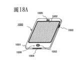
1000:行動電話1000: Mobile phone
1001:外殼1001: Shell
1002:顯示部1002: Display unit
1003:操作按鈕1003: Operation button
1004:外部連接埠1004: External port
1005:揚聲器1005: Speaker
1006:麥克風1006: Microphone
1300:基板1300: Substrate
1301:顯示部1301: Display unit
1302:驅動部1302: Drive Department
1303:信號線驅動器電路1303:Signal line driver circuit
1304:掃描線驅動器電路1304: Scan line driver circuit
1305:像素1305: pixels
1306:掃描線1306: Scan line
1308:信號線1308:Signal line
1309:外部連接終端1309: External connection terminal
1400:基板1400: Substrate
1401:閘極電極層1401: Gate electrode layer
1402:閘極絕緣層1402: Gate insulation layer
1403:氧化物半導體層1403: Oxide semiconductor layer
1405a:源極電極層1405a: Source electrode layer
1405b:汲極電極層1405b: Drain electrode layer
1418:通道保護層1418: Channel protection layer
1430:薄膜電晶體1430:Thin Film Transistor
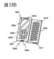
1800:外殼1800: Shell
1801:外殼1801: Shell
1802:顯示面板1802: Display panel
1803:揚聲器1803: Speaker
1804:麥克風1804: Microphone
1805:操作鍵1805: Operation keys
1806:定位裝置1806: Positioning device
1807:相機透鏡1807: Camera lens
1808:外部連接終端1808: External connection terminal
1810:鍵盤1810:Keyboard
1811:外部記憶卡插槽1811: External memory card slot
1908:顯示面板1908: Display panel
1920:基板1920: Substrate
1921:顯示部1921: Display Department
1922:密封劑1922: Sealant
1923:基板1923: Substrate
1924:撓性印刷電路1924: Flexible printed circuits
1925:第一密封劑1925: The first sealant
1926:第二密封劑1926: Second sealant
1927:驅動器積體電路1927: Driver integrated circuit
6400:像素6400: pixels
6401:交換電晶體6401: Switching transistor
6402:驅動電晶體6402:Drive transistor
6403:電容器6403:Capacitor
6404:發光元件6404: Light-emitting element
6405:信號線6405:Signal line
6406:掃描線6406: Scan line
6407:電源線6407: Power cord
6408:共同電極6408: Common electrode
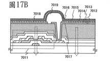
7001:驅動薄膜電晶體7001: Driving thin film transistors
7002:發光元件7002: Light-emitting element
7003:陰極7003: cathode
7004:發光層7004: Luminescent layer
7005:陽極7005: Yang pole
7006:保護絕緣層7006: Protective insulation layer
7007:平面化絕緣膜7007: Planarization insulation film
7008:陰極7008: cathode
7009:隔牆7009: Partition wall
7011:驅動薄膜電晶體7011: Driving thin film transistors
7012:發光元件7012: Light-emitting element
7013:陰極7013: cathode
7014:發光層7014: Luminescent layer
7015:陽極7015: Yang pole
7016:阻光膜7016: Light-blocking film
7017:具有光透射特性之導電膜7017: Conductive film with light-transmitting properties
7018:陰極7018: cathode
7019:隔牆7019: Partition wall
7021:驅動薄膜電晶體7021: Driving thin film transistors
7022:發光元件7022: Light-emitting element
7023:陰極7023: cathode
7024:發光層7024: Luminescent layer
7025:陽極7025: Yang pole
7027:具有光透射特性之導電膜7027: Conductive film with light-transmitting properties
7028:陰極7028: cathode
7029:隔牆7029: Partition
9600:電視機9600:TV
9601:外殼9601: Shell
9603:顯示部9603: Display unit
9605:座9605: Seat
9607:顯示部9607: Display unit
9609:操作鍵9609: Operation key
9610:遙控器9610: Remote control
9700:數位相框9700: Digital photo frame
9701:外殼9701: Shell
9703:顯示部9703: Display unit
9881:外殼9881: Shell
9882:顯示部9882: Display unit
9883:顯示部9883: Display unit
9884:揚聲器部9884: Speaker unit
9885:操作鍵9885: Operation key
9886:記錄媒體插入部9886: Recording media insertion unit
9887:連接終端9887:Connecting terminal
9888:感測器9888:Sensor
9889:麥克風9889: Microphone
9890:發光二極體燈9890:LED lamp
9891:外殼9891: Shell
9893:連接部9893:Connection part
在附圖中:In the attached picture:
圖1A至1C為本發明的一實施例之製造步驟的橫剖面圖;Figures 1A to 1C are cross-sectional views of the manufacturing steps of an embodiment of the present invention;
圖2A及2B分別為本發明的一實施例之平面圖和橫剖面圖;Figures 2A and 2B are respectively a plan view and a cross-sectional view of an embodiment of the present invention;
圖3A至3D為本發明的一實施例之製造步驟的橫剖面圖;Figures 3A to 3D are cross-sectional views of the manufacturing steps of an embodiment of the present invention;
圖4A至4C為本發明的一實施例之製造步驟的橫剖面圖;Figures 4A to 4C are cross-sectional views of the manufacturing steps of an embodiment of the present invention;
圖5A至5C為本發明的一實施例之製造步驟的橫剖面圖;Figures 5A to 5C are cross-sectional views of the manufacturing steps of an embodiment of the present invention;
圖6A及6B分別為本發明的一實施例之平面圖和橫剖面圖;Figures 6A and 6B are respectively a plan view and a cross-sectional view of an embodiment of the present invention;
圖7A及7B為本發明的一實施例之製造步驟的橫剖面圖,及圖7C為本發明的一實施例之平面圖;Figures 7A and 7B are cross-sectional views of the manufacturing steps of an embodiment of the present invention, and Figure 7C is a plan view of an embodiment of the present invention;
圖8A至8D為本發明的一實施例之製造步驟的橫剖面圖;Figures 8A to 8D are cross-sectional views of the manufacturing steps of an embodiment of the present invention;
圖9A至9C為本發明的一實施例之製造步驟的橫剖面圖;Figures 9A to 9C are cross-sectional views of the manufacturing steps of an embodiment of the present invention;
圖10為本發明的一實施例之平面圖;Figure 10 is a plan view of an embodiment of the present invention;
圖11為本發明的一實施例之平面圖;Figure 11 is a plan view of an embodiment of the present invention;
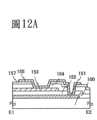
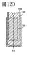
圖12A及12C為本發明的一實施例之橫剖面圖而圖12B及12D為其平面圖;Figures 12A and 12C are cross-sectional views of an embodiment of the present invention and Figures 12B and 12D are plan views thereof;
圖13A至13C為本發明的一實施例之立體圖;Figures 13A to 13C are three-dimensional diagrams of an embodiment of the present invention;
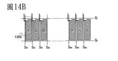
圖14A及14B為本發明的一實施例之方塊圖;Figures 14A and 14B are block diagrams of an embodiment of the present invention;
圖15為本發明的一實施例之時序圖;Figure 15 is a timing diagram of an embodiment of the present invention;
圖16為半導體裝置中的像素之等效電路圖;Figure 16 is an equivalent circuit diagram of a pixel in a semiconductor device;
圖17A至17C各個為半導體裝置的橫剖面圖;Figures 17A to 17C are each a cross-sectional view of a semiconductor device;
圖18A及18B各個為半導體裝置圖;Figures 18A and 18B are each a semiconductor device diagram;
圖19A及19B各個為半導體裝置圖;以及Figures 19A and 19B are each a semiconductor device diagram; and
圖20為半導體裝置圖。Figure 20 is a diagram of a semiconductor device.
下面,將參考附圖詳細說明本發明的實施例。然而,本發明並不侷限於下面說明,精於本技藝之人士應容易明白,可以各種方式修改此處所揭示之模式和細節。因此,本發明不應被解釋成侷限於實施例的說明。Below, the embodiments of the present invention will be described in detail with reference to the attached drawings. However, the present invention is not limited to the following description, and it should be easy for those skilled in the art to understand that the modes and details disclosed herein can be modified in various ways. Therefore, the present invention should not be interpreted as being limited to the description of the embodiments.
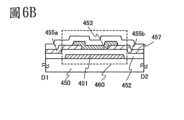
將參考圖1A至1C及圖2A及2B說明半導體裝置及半導體裝置之製造方法。在圖2B中,圖解為稱作通道蝕刻型之結構的其中一類型之薄膜電晶體470。A semiconductor device and a method for manufacturing the semiconductor device will be described with reference to FIGS. 1A to 1C and FIGS. 2A and 2B. In FIG. 2B, a
圖2A為包括在半導體裝置中之薄膜電晶體470的平面圖,及圖2B為沿著圖2A的線C1-C2所取之橫剖面圖。薄膜電晶體470為底閘極薄膜電晶體,及包括閘極電極層401、閘極絕緣層402、氧化物半導體層403、源極電極層405a、及汲極電極層405b在具有絕緣表面的基板400上。此外,氧化物絕緣膜407係設置成覆蓋薄膜電晶體470並且與氧化物半導體層403接觸。FIG. 2A is a plan view of a
具有絕緣表面的基板400、閘極電極層401、閘極絕緣層402、氧化物半導體層403、源極電極層405a、汲極電極層405b、及氧化物絕緣膜407係都使用具有可見光透射特性的材料來形成。因此,在將薄膜電晶體470置放於顯示裝置的像素部中之例子中,薄膜電晶體470具有光透射特性並且可提高孔徑比。The
關於氧化物半導體層403,至少在形成氧化物半導體膜之後,執行用以降低雜質的濕氣等熱處理(用於脫水作用或除氫作用的熱處理)。用於脫水作用或除氫作用的熱處理和慢速冷卻接在形成與氧化物半導體層接觸的氧化物絕緣膜等之後;因此,氧化物半導體層的載子被降低,以提高薄膜電晶體470的可靠性。Regarding the
不僅在氧化物半導體層403中,並且也在閘極絕緣層402中,在氧化物半導體層403和上方的薄膜之間且與之接觸以及在氧化物半導體層403和下方的膜之間和與之接觸的介面中降低諸如濕氣等雜質,尤其是在閘極絕緣層402和氧化物半導體層403之間的介面以及氧化物絕緣膜407和氧化物半導體層403之間的介面。Impurities such as moisture are reduced not only in the
下面,圖1A至1C為說明圖2B所示之薄膜電晶體470的製造處理之橫剖面圖。Below, Figures 1A to 1C are cross-sectional views illustrating the manufacturing process of the
在圖1A中,閘極電極層401係設置在具有絕緣表面的基板400上。In FIG. 1A , a
雖然沒有特別限制可被使用作為具有絕緣表面的基板400之基板,但是基板必須至少對稍候將執行的熱處理具有足夠的耐熱性。作為具有絕緣表面的基板400,可使用由鋇硼矽酸鹽玻璃、鋁硼矽酸鹽玻璃等所形成的玻璃基板。Although there is no particular limitation on the substrate that can be used as the
在使用玻璃基板並且稍候欲執行熱處理的溫度高之例子中,使用應變點大於或等於730℃之玻璃基板較佳。作為玻璃基板,例如使用諸如鋁矽酸鹽玻璃、鋁硼矽酸鹽玻璃、或鋇硼矽酸鹽玻璃等玻璃材料。需注意的是,藉由含有氧化鋇(BaO)的量多於硼酸,玻璃基板耐熱且更實用。因此,使用含有BaO及B2O3的玻璃基板,使得BaO的量大於B2O3的量較佳。In the case where a glass substrate is used and the temperature of heat treatment to be performed later is high, it is preferable to use a glass substrate having a strain point greater than or equal to 730°C. As the glass substrate, for example, glass materials such as aluminosilicate glass, aluminum borosilicate glass, or barium borosilicate glass are used. It should be noted that by containing more barium oxide (BaO) than boricacid , the glass substrate is heat-resistant and more practical. Therefore, it is preferable to use a glass substrate containing BaO andB2O3 so that the amount of BaO is greater thanthe amount ofB2O3 .
需注意的是,可使用由諸如陶瓷基板、石英基板、或藍寶石基板等絕緣體所形成的基板,來取代上述玻璃基板。其他選擇是,亦可使用結晶玻璃。It should be noted that a substrate formed of an insulator such as a ceramic substrate, a quartz substrate, or a sapphire substrate may be used instead of the above-mentioned glass substrate. Alternatively, crystallized glass may be used.
另外,充作基膜的絕緣膜係可設置在基板400和閘極電極層401之間。基膜具有防止雜質元素擴散到基板400的功能,及可被形成具有使用一或多個氮化矽膜、氧化矽膜、氧氮化矽膜、及氮氧化矽膜之單層或疊層結構。In addition, an insulating film serving as a base film may be disposed between the
作為閘極電極層401的材料,可利用諸如下面材料等具有光透射特性的導電材料:In-Sn-Zn-O為基的金屬氧化物、In-Al-Zn-O為基的金屬氧化物、Sn-Ga-Zn-O為基的金屬氧化物、Al-Ga-Zn-O為基的金屬氧化物、Sn-Al-Zn-O為基的金屬氧化物、In-Zn-O為基的金屬氧化物、Sn-Zn-O為基的金屬氧化物、Al-Zn-O為基的金屬氧化物、In-O為基的金屬氧化物、Sn-O為基的金屬氧化物、和Zn-O為基的金屬氧化物。適當選擇閘極電極層401的厚度在30nm至200nm的範圍內。作為用於閘極電極層401之金屬氧化物的沈積方法,可使用濺鍍法、真空蒸發法(電子束蒸發法等)、電弧放電離子電鍍法、或噴灑法。As the material of the
接著,將閘極絕緣層402形成在閘極電極層401上。Next, a
閘極絕緣層402可藉由電漿CVD法、濺鍍法等被形成具有使用氧化矽層、氮化矽層、氮氧化矽層、氧氮化矽層之單層或疊層結構。例如,可藉由電漿CVD法,使用SiH4、氧、和氮作為膜形成氣體來形成氮氧化矽層。The
然後,在閘極絕緣層402上,氧化物半導體膜被形成具有大於或等於2nm及小於或等於200nm的厚度。Then, on the
需注意的是,在藉由濺鍍法形成氧化物半導體膜之前,藉由引進氬氣及產生電漿之逆濺鍍去除閘極絕緣層402的表面上之灰塵較佳。逆濺鍍意指在未施加電壓到目標側之下,在氬大氣中使用RF電源來施加電壓到基板側,以在基板附近產生電漿,以修改表面之方法。需注意的是,可使用氮、氦、氧等來取代氬。It should be noted that before forming an oxide semiconductor film by sputtering, dust on the surface of the
氧化物半導體膜係藉由使用In-Ga-Zn-O為基的氧化物半導體目標,以濺鍍法來形成。其他選擇是,氧化物半導體膜係可在稀有氣體(典型上為氬)中、在氧氛圍中、或在包括稀有氣體(典型上為氬)和氧的大氣中以濺鍍法形成。The oxide semiconductor film is formed by sputtering using an In-Ga-Zn-O-based oxide semiconductor target. Alternatively, the oxide semiconductor film may be formed by sputtering in a rare gas (typically argon), in an oxygen atmosphere, or in an atmosphere including a rare gas (typically argon) and oxygen.
可在未暴露至空氣之下連續形成閘極絕緣層402和氧化物半導體膜。當在未暴露至空氣之下連續形成閘極絕緣層402和氧化物半導體膜時,可在未被諸如濕氣或碳氫化合物等大氣組成或空氣中飄浮的雜質元素污染其介面之下來形成閘極絕緣層402和氧化物半導體膜。因此,可降低薄膜電晶體之間的特性變化。The
然後,藉由光致微影步驟將氧化物半導體膜處理成氧化物半導體層(第一氧化物半導體層430),其為島型氧化物半導體層(見圖1A)。Then, the oxide semiconductor film is processed into an oxide semiconductor layer (first oxide semiconductor layer 430) by a photolithography step, which is an island-type oxide semiconductor layer (see FIG. 1A).
接著,將第一氧化物半導體層430脫水或除氫。執行用於脫水作用或除氫作用之第一熱處理的溫度大於或等於350℃且低於基板的應變點,大於或等於400℃較佳。此處,將基板引進熱處理設備的其中之一的電爐中,及在氧氛圍中將第一氧化物半導體層430經過熱處理;然後,在氧氛圍中執行慢速冷卻,藉以形成第二氧化物半導體層431(見圖1B)。從將氧化物半導體層脫水或除氫之加熱溫度T到足夠低到防止水再次進入之溫度執行慢速冷卻,尤其是到低於加熱溫度T之大於100℃的溫度。其他選擇是,將慢速冷卻執行到低於稍後執行之第二熱處理的溫度之溫度,然後將基板從熱處理的設備取出。氧化物半導體層在氧氛圍中接受熱處理,藉以可去除含在氧化物半導體層中諸如水等雜質,及同時,使第二氧化物半導體層431成為氧過量的狀態。依據第一熱處理的條件或氧化物半導體層的材料,在一些例子中,氧化物半導體層被結晶且變成微晶膜或複晶膜。Next, the first
需注意的是,在第一熱處理中,水、氫等未包含在氧氣中較佳。其他選擇是,引進熱處理設備內之氧氣的純淨大於或等於6N(99.9999%)較佳,大於或等於7N(99.99999%)更好(即、氧氣中的雜質濃度低於或等於1ppm,或者低於或等於0.1ppm較佳)。It should be noted that in the first heat treatment, water, hydrogen, etc. are preferably not included in the oxygen. Another option is that the purity of the oxygen introduced into the heat treatment equipment is preferably greater than or equal to 6N (99.9999%), and greater than or equal to 7N (99.99999%) (that is, the impurity concentration in the oxygen is less than or equal to 1ppm, or less than or equal to 0.1ppm).
執行第一熱處理達大於或等於0.5小時和低於或等於10小時,其中電爐的溫度增加比率大於或等於0.1℃/min及小於或等於20℃/min較佳。另外,電爐的溫度減少比率大於或等於0.1℃/min及小於或等於15℃/min較佳。The first heat treatment is performed for greater than or equal to 0.5 hours and less than or equal to 10 hours, wherein the temperature increase rate of the electric furnace is preferably greater than or equal to 0.1°C/min and less than or equal to 20°C/min. In addition, the temperature decrease rate of the electric furnace is preferably greater than or equal to 0.1°C/min and less than or equal to 15°C/min.
結果,可提高稍後欲形成的薄膜電晶體之可靠性。As a result, the reliability of the thin film transistor to be formed later can be improved.
另外,取代使用電爐的加熱法,諸如使用加熱氣體之氣體快速熱退火(GRTA)法等快速加熱法,或者使用燈光之燈快速熱退火(LRTA)法可被用於第一熱處理。In addition, instead of the heating method using an electric furnace, a rapid heating method such as a gas rapid thermal annealing (GRTA) method using a heating gas, or a lamp rapid thermal annealing (LRTA) method using lamps may be used for the first heat treatment.
在熱處理設備為多室型之例子中,用於第一熱處理之室可不同於冷卻處理之室。典型上,在填滿氧氣且其溫度增加到大於或等於400℃且低於基板的應變點之第一室中加熱基板上的氧化物半導體層。然後,經由引進氧氣之轉移室,執行上述第一熱處理之基板被轉移到填滿氧且其溫度低於或等於100℃或室溫較佳之第二室內,及接受冷卻處理。經由上述步驟,可提高生產量。In the case where the heat treatment equipment is a multi-chamber type, the chamber used for the first heat treatment may be different from the chamber for the cooling treatment. Typically, the oxide semiconductor layer on the substrate is heated in the first chamber filled with oxygen and whose temperature is increased to greater than or equal to 400°C and lower than the strain point of the substrate. Then, through the transfer chamber into which oxygen is introduced, the substrate subjected to the above-mentioned first heat treatment is transferred to the second chamber filled with oxygen and whose temperature is lower than or equal to 100°C or preferably room temperature, and subjected to cooling treatment. Through the above steps, the production capacity can be improved.
其他選擇是,在處理成島型氧化物半導體層之前的氧化物半導體膜亦可在氧氛圍中接受第一熱處理。在那例子中,在氧化物半導體膜的第一熱處理和冷卻處理之後,從加熱裝置取出基板,及執行光致微影步驟。Alternatively, the oxide semiconductor film may be subjected to a first heat treatment in an oxygen atmosphere before the island-type oxide semiconductor layer is processed. In that case, after the first heat treatment and cooling treatment of the oxide semiconductor film, the substrate is removed from the heating device and a photolithography step is performed.
在形成氧化物半導體膜之前,在鈍氣(氮或諸如氦、氖、或氬等稀有氣體)大氣中、在氧氛圍中、或減壓下,閘極絕緣層可接受熱處理(在大於或等於400℃且低於基板的應變點之溫度中),使得層中之諸如氫和水等雜質被去除。Before forming the oxide semiconductor film, the gate insulating layer may be subjected to heat treatment (at a temperature greater than or equal to 400°C and lower than the strain point of the substrate) in a passivation gas (nitrogen or a rare gas such as helium, neon, or argon) atmosphere, in an oxygen atmosphere, or under reduced pressure, so that impurities such as hydrogen and water in the layer are removed.
接著,將導電膜形成在閘極絕緣層402和第二氧化物半導體層431上。作為導電膜的沈積法,使用濺鍍法、真空蒸發法(電子束蒸發法等)、電弧放電離子電鍍法、或噴灑法等。Next, a conductive film is formed on the
作為導電膜的材料,可利用諸如下面材料等具有可見光透射特性之導電材料:In-Sn-Zn-O為基的金屬氧化物、In-Al-Zn-O為基的金屬氧化物、Sn-Ga-Zn-O為基的金屬氧化物、Al-Ga-Zn-O為基的金屬氧化物、Sn-Al-Zn-O為基的金屬氧化物、In-Zn-O為基的金屬氧化物、Sn-Zn-O為基的金屬氧化物、Al-Zn-O為基的金屬氧化物、In-O為基的金屬氧化物、Sn-O為基的金屬氧化物、和Zn-O為基的金屬氧化物。適當選擇導電膜的厚度在30nm至200nm的範圍內。As the material of the conductive film, conductive materials having visible light transmission characteristics such as the following materials can be used: In-Sn-Zn-O-based metal oxides, In-Al-Zn-O-based metal oxides, Sn-Ga-Zn-O-based metal oxides, Al-Ga-Zn-O-based metal oxides, Sn-Al-Zn-O-based metal oxides, In-Zn-O-based metal oxides, Sn-Zn-O-based metal oxides, Al-Zn-O-based metal oxides, In-O-based metal oxides, Sn-O-based metal oxides, and Zn-O-based metal oxides. The thickness of the conductive film is appropriately selected within the range of 30nm to 200nm.
然後,藉由光致微影步驟選擇性蝕刻第二氧化物半導體層431和導電膜,以形成氧化物半導體層403、源極電極層405a、及汲極電極層405b。需注意的是,只有氧化物半導體層的部分被蝕刻成具有溝槽(凹下部)之氧化物半導體層。當在去除此光致微影步驟中所使用的抗蝕遮罩中執行氧灰化時,將氧引進氧化物半導體層的露出區域。Then, the second
接著,充作保護絕緣層的氧化物絕緣膜407被形成與氧化物半導體層403的部分接觸,藉以可製造薄膜電晶體470(見圖1C)。氧化物絕緣膜407被形成具有至少大於或等於1nm的厚度,且可藉由防止諸如水或氫等雜質進入氧化物絕緣膜407之方法來適當形成,例如,藉由CVD法或濺鍍法。此處,氧化物絕緣膜407係藉由濺鍍法來形成。形成與低電阻氧化物半導體層接觸之氧化物絕緣膜407未含有諸如濕氣、氫離子、或OH-等雜質,及係使用防止這些從外面侵入之無機絕緣膜所形成。典型上,使用氧化矽膜、氧氮化矽膜、氧化鋁膜、或氮氧化鋁膜。其他選擇是,可形成在氧化物絕緣膜407上並且與氧化物絕緣膜407接觸之氮化矽膜或氮化鋁膜。氮化矽膜未含有諸如濕氣、氫離子、或OH-等雜質,及防止這些從外面侵入。Next, an
在此實施例中,具有厚度300nm之氧化矽膜被形成作氧化物絕緣膜407。膜形成時之基板溫度可大於或等於室溫且低於或等於300℃;在此實施例中,基板溫度是100℃。可在稀有氣體(典型上為氬)大氣中、氧氛圍中、或包括氧化矽膜稀有氣體(典型上為氬)和氧的大氣中,以濺鍍法來形成氧化矽膜。作為目標,可使用氧化矽目標或矽目標;例如,氧化矽膜係可在包括氧和氮的大氣中,以濺鍍法,使用矽目標來形成。In this embodiment, a silicon oxide film having a thickness of 300 nm is formed as an
另外,在形成氧化物絕緣膜407之後,薄膜電晶體470可在氮氛圍或在氧氛圍中接受第二熱處理(在大於或等於150℃及低於350℃的溫度中較佳)。例如,在氮氛圍中以250℃執行第二熱處理達一小時。藉由第二熱處理,在氧化物半導體層403與氧化物絕緣膜407接觸的同時加熱氧化物半導體層403;如此,可降低薄膜電晶體470中的電特性變化。In addition, after the
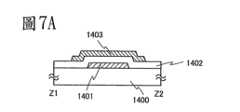
將參考圖3A至3D說明不同於實施例1之半導體裝置和半導體裝置製造方法。完全相同或具有類似於實施例1者的功能之部位係可以類似於實施例1所說明的方式之方式來形成;因此,省略重複說明。A semiconductor device and a method for manufacturing a semiconductor device different from
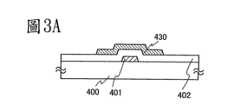
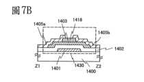
圖3A至3D為薄膜電晶體480的製造處理之橫剖面圖。圖3D所示之薄膜電晶體480的結構被稱作反向共面型(亦稱作底接觸型)。3A to 3D are cross-sectional views of the manufacturing process of the
與實施例1類似,閘極電極層401係設置在具有絕緣表面的基板400上。充作基膜的絕緣膜係可設置在基板400和閘極電極層401之間。Similar to
接著,與實施例1類似,閘極絕緣層402係形成在閘極電極層401上。然後,氧化物半導體膜係形成在閘極絕緣層402上。Next, similar to
然後,藉由光致微影步驟將氧化物半導體膜處理成氧化物半導體層(第一氧化物半導體層430),其為島型氧化物半導體層(見圖3A)。需注意的是,圖3A與圖1A相同。Then, the oxide semiconductor film is processed into an oxide semiconductor layer (first oxide semiconductor layer 430) by a photolithography step, which is an island-type oxide semiconductor layer (see FIG. 3A). It should be noted that FIG. 3A is the same as FIG. 1A.
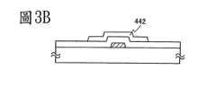
接著,將第一氧化物半導體層430脫水或除氫。執行用於脫水作用或除氫作用之第一熱處理的溫度大於或等於350℃且低於基板的應變點,大於或等於400℃較佳。此處,將基板引進熱處理設備的其中之一的電爐中,及在鈍氣(氮或諸如氦、氖、或氬等稀有氣體)大氣中或減壓下,將第一氧化物半導體層430接受熱處理,藉以形成第二氧化物半導體層442(見圖3B)。藉由在鈍氣大氣中或減壓下的熱處理,氧化物半導體層的電阻被降低(其載子濃度增加到大於或等於1×10¹⁸/cm3較佳),及可形成低電阻氧化物半導體層(第二氧化物半導體層442)。Next, the first
需注意的是,在第一熱處理中,水、氫等未包含在氮或諸如氦、氖、或氬等稀有氣體中較佳。其他選擇是,引進到熱處理設備中之氮或諸如氦、氖、或氬等稀有氣體的純淨大於或等於6N較佳,或大於或等於7N更好(即、雜質濃度低於或等於1ppm,或低於或等於0.1ppm較佳)。在此實施例中,藉由加熱具有氮氛圍且引進基板之電爐到大於或等於350℃及低於或等於600℃的溫度,或大於或等於400℃較佳,來執行脫水作用或除氫作用;然後,停止氮或稀有氣體及關掉加熱器。It should be noted that in the first heat treatment, water, hydrogen, etc. are preferably not contained in nitrogen or rare gases such as helium, neon, or argon. Another option is that the purity of nitrogen or rare gases such as helium, neon, or argon introduced into the heat treatment equipment is preferably greater than or equal to 6N, or greater than or equal to 7N (i.e., the impurity concentration is less than or equal to 1ppm, or less than or equal to 0.1ppm). In this embodiment, dehydration or dehydrogenation is performed by heating the electric furnace with a nitrogen atmosphere and the substrate introduced to a temperature greater than or equal to 350°C and less than or equal to 600°C, or greater than or equal to 400°C; then, the nitrogen or rare gas is stopped and the heater is turned off.
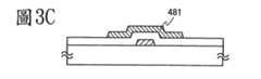
在加熱之後,在氧氛圍中執行慢速冷卻,使得第三氧化物半導體481被形成(見圖3C)。從氧化物半導體層被脫水或除氫的加熱溫度T至足夠低到防止水再次進來的溫度來執行慢速冷卻,尤其是至大於100℃低於加熱溫度T之溫度。其他選擇是,在氧氛圍中執行慢速冷卻到低於稍後欲執行之第二熱處理的溫度,然後從熱處理設備取出基板。在此實施例中,在關掉電爐的加熱器及引進氧到電爐內之後執行慢速冷卻。較佳的是,諸如水或氫等雜質未包含在所引進的氧中較佳。其他選擇是,從氣體供應源引進到室內之氧的純淨低於或等於6N,或低於或等於7N較佳(即、氧氣中的雜質濃度低於或等於1ppm,或者低於或等於0.1ppm較佳)。After heating, slow cooling is performed in an oxygen atmosphere so that a
結果,可提高稍後欲形成之薄膜電晶體的可靠度。As a result, the reliability of the thin film transistor to be formed later can be improved.
需注意的是,在減壓下執行第一熱處理的例子中,可在熱處理之後藉由引進氧到電爐內以及將壓力回到大氣壓力,來執行冷卻。It should be noted that in the case where the first heat treatment is performed under reduced pressure, cooling can be performed after the heat treatment by introducing oxygen into the electric furnace and returning the pressure to atmospheric pressure.
在熱處理設備為多室型之例子中,用於第一熱處理的室可不同於冷卻處理用的室。典型上,在填滿氮或稀有氣體且其溫度增加到大於或等於400℃及低於基板的應變點之第一室加熱基板上的氧化物半導體層。然後,執行慢速冷卻到足以低到防止水再次進來的溫度,尤其是,到低於加熱溫度T之大於100℃的溫度。接著,經由引進氮或稀有氣體之轉移室,執行上述第一熱處理之基板被轉移到填滿氧且其溫度低於或等於100℃或室溫較佳之第二室,及接受冷卻處理。經由上述步驟,可提高生產量。In the case where the heat treatment equipment is a multi-chamber type, the chamber used for the first heat treatment may be different from the chamber used for the cooling treatment. Typically, the oxide semiconductor layer on the substrate is heated in the first chamber which is filled with nitrogen or a rare gas and whose temperature is increased to greater than or equal to 400°C and lower than the strain point of the substrate. Then, slow cooling is performed to a temperature low enough to prevent water from entering again, in particular, to a temperature greater than 100°C lower than the heating temperatureT. Next, the substrate subjected to the above-mentioned first heat treatment is transferred to a second chamber filled with oxygen and whose temperature is lower than or equal to 100°C or preferably room temperature, through a transfer chamber into which nitrogen or a rare gas is introduced, and subjected to cooling treatment. Through the above steps, the throughput can be improved.
其他選擇是,在被處理成島型氧化物半導體層之前的氧化物半導體膜亦可在鈍氣大氣中或減壓下接受第一熱處理。在那例子中,在第一熱處理和冷卻處理之後,從加熱裝置取出基板,及執行光致微影步驟。Alternatively, the oxide semiconductor film before being processed into the island-type oxide semiconductor layer may also be subjected to a first heat treatment in a passive atmosphere or under reduced pressure. In that case, after the first heat treatment and cooling treatment, the substrate is removed from the heating device and a photolithography step is performed.
在形成氧化物半導體膜之前,可在鈍氣(氮或諸如氦、氖、或氬等稀有氣體)大氣中、在氧氛圍中、或減壓下,使閘極絕緣層接受熱處理(在大於或等於400℃和低於基板的應變點之溫度),使得層中的諸如氫和水等雜質被去除。Before forming the oxide semiconductor film, the gate insulating layer can be subjected to heat treatment (at a temperature greater than or equal to 400°C and lower than the strain point of the substrate) in a passivation gas (nitrogen or rare gases such as helium, neon, or argon) atmosphere, in an oxygen atmosphere, or under reduced pressure, so that impurities such as hydrogen and water in the layer are removed.
然後,將導電膜形成在閘極絕緣層402和第三氧化物半導體層481上。Then, a conductive film is formed on the
作為導電膜的材料,可利用諸如下面材料等具有可見光透射特性的導電材料:In-Sn-Zn-O為基的金屬氧化物、In-Al-Zn-O為基的金屬氧化物、Sn-Ga-Zn-O為基的金屬氧化物、Al-Ga-Zn-O為基的金屬氧化物、Sn-Al-Zn-O為基的金屬氧化物、In-Zn-O為基的金屬氧化物、Sn-Zn-O為基的金屬氧化物、Al-Zn-O為基的金屬氧化物、In-O為基的金屬氧化物、Sn-O為基的金屬氧化物、和Zn-O為基的金屬氧化物。適當選擇導電膜的厚度在30nm至200nm的範圍內。As the material of the conductive film, conductive materials having visible light transmission characteristics such as the following materials can be used: In-Sn-Zn-O-based metal oxides, In-Al-Zn-O-based metal oxides, Sn-Ga-Zn-O-based metal oxides, Al-Ga-Zn-O-based metal oxides, Sn-Al-Zn-O-based metal oxides, In-Zn-O-based metal oxides, Sn-Zn-O-based metal oxides, Al-Zn-O-based metal oxides, In-O-based metal oxides, Sn-O-based metal oxides, and Zn-O-based metal oxides. The thickness of the conductive film is appropriately selected within the range of 30nm to 200nm.
然後,藉由光致微影步驟選擇性蝕刻第三氧化物半導體層481和導電膜,以形成氧化物半導體層483、源極電極層405a、和汲極電極層405b。需注意的是,只有氧化物半導體層的部分被蝕刻成具有溝槽(凹下部)的氧化物半導體層。當在去除此光致微影步驟中所使用之抗蝕遮罩中執行氧灰化時,將氧引進氧化物半導體層的露出區域。Then, the third
接著,充作保護絕緣層之氧化物絕緣膜407被形成與氧化物半導體層483的部分接觸,藉以可製造薄膜電晶體480(見圖3D)。氧化物絕緣膜407被形成具有至少大於或等於1nm的厚度,及可藉由防止諸如水或氫等雜質進入氧化物絕緣膜407之方法來適當形成,例如,藉由CVD法或濺鍍法。此處,氧化物絕緣膜407係藉由濺鍍法所形成。被形成與低電阻氧化物半導體層接觸之氧化物絕緣膜407未含有諸如濕氣、氫離子、或OH-等雜質,及使用防止這些從外面侵入之無機絕緣膜來形成。典型上,使用氧化矽膜、氧氮化矽膜、氧化鋁膜、或氮氧化鋁膜。其他選擇是,可形成在氧化物絕緣膜407上及與氧化物絕緣膜407接觸氮化矽膜或氮化鋁膜。氮化矽膜未含有諸如濕氣、氫離子、或OH-等雜質,及防止這些從外面侵入。Next, an
在此實施例中,具有厚度300nm的氧化矽膜被形成作為氧化物絕緣膜407。膜形成時的基板溫度可大於或等於室溫及小於或等於300℃;在此實施例中,基板溫度是100℃。氧化矽膜係可在稀有氣體(典型上為氬)大氣中、在氧氛圍中、或在包括稀有氣體(典型上為氬)和氧的大氣中,以濺鍍法來形成。作為目標,可使用氧化矽目標或矽目標;例如,氧化矽膜係可在包括氧和氮的大氣中,以濺鍍法,使用矽目標來形成。In this embodiment, a silicon oxide film having a thickness of 300 nm is formed as the
另外,在形成氧化物絕緣膜407之後,薄膜電晶體480可在氮氛圍或在氧氛圍中接受第二熱處理(在大於或等於150℃及低於350℃的溫度中較佳)。例如,在氮氛圍中以250℃執行第二熱處理達一小時。藉由第二熱處理,在氧化物半導體層483與氧化物絕緣膜407接觸的同時加熱氧化物半導體層483;如此,可降低薄膜電晶體480中的電特性變化。In addition, after the
此實施例可與實施例1自由組合。This embodiment can be freely combined with
將參考圖4A至4C說明不同於實施例1及2之半導體裝置和半導體裝置製造方法。完全相同或具有類似於實施例1及2者的功能之部位係可以類似於實施例1及2所說明的方式之方式來形成;因此,省略重複說明。A semiconductor device and a method for manufacturing a semiconductor device different from those in Examples 1 and 2 will be described with reference to FIGS. 4A to 4C. Parts having functions that are completely identical to or similar to those in Examples 1 and 2 can be formed in a manner similar to that described in Examples 1 and 2; therefore, repeated descriptions are omitted.
圖4A至4C為薄膜電晶體440的製造處理之橫剖面圖。圖4C所示之薄膜電晶體440的結構被稱作通道停止型。4A to 4C are cross-sectional views of the manufacturing process of the
與實施例1類似,閘極電極層401係設置在具有絕緣表面的基板400上。充作基膜的絕緣膜係可設置在基板400和閘極電極層401之間。Similar to
接著,與實施例1類似,閘極絕緣層402係形成在閘極電極層401上。然後,氧化物半導體膜係形成在閘極絕緣層402上。Next, similar to
然後,藉由光致微影步驟將氧化物半導體膜處理成氧化物半導體層(第一氧化物半導體層430),其為島型氧化物半導體層(見圖4A)。需注意的是,圖4A與圖1A相同。Then, the oxide semiconductor film is processed into an oxide semiconductor layer (first oxide semiconductor layer 430) by a photolithography step, which is an island-type oxide semiconductor layer (see FIG. 4A). It should be noted that FIG. 4A is the same as FIG. 1A.
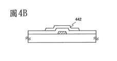
接著,將第一氧化物半導體層430脫水或除氫。執行用於脫水作用或除氫作用之第一熱處理的溫度大於或等於350℃且低於基板的應變點,大於或等於400℃較佳。此處,將基板引進熱處理設備的其中之一的電爐中,及在鈍氣(氮或諸如氦、氖、或氬等稀有氣體)大氣中或減壓下,將第一氧化物半導體層430接受熱處理,藉以形成第二氧化物半導體層444(見圖4B)。Next, the first
需注意的是,在第一熱處理中,水、氫等未包含在氮或諸如氦、氖、或氬等稀有氣體中較佳。其他選擇是,引進到熱處理設備中之氮或諸如氦、氖、或氬等稀有氣體的純淨大於或等於6N(99.9999%)較佳,或大於或等於7N(99.99999%)更好(即、雜質濃度低於或等於1ppm,或低於或等於0.1ppm較佳)。在此實施例中,藉由加熱具有氮氛圍且引進基板之電爐到大於或等於350℃及低於或等於600℃的溫度,或大於或等於400℃較佳,來執行脫水作用或除氫作用;然後,關掉加熱器及執行慢速冷卻。藉由在鈍氣大氣中或減壓下的熱處理和慢速冷卻,氧化物半導體層的電阻被降低(其載子濃度增加到大於或等於1×10¹⁸/cm3較佳),及可形成低電阻氧化物半導體層(第二氧化物半導體層444)。It should be noted that in the first heat treatment, water, hydrogen, etc. are preferably not contained in nitrogen or rare gases such as helium, neon, or argon. Alternatively, the purity of nitrogen or rare gases such as helium, neon, or argon introduced into the heat treatment equipment is preferably greater than or equal to 6N (99.9999%), or greater than or equal to 7N (99.99999%) (i.e., the impurity concentration is less than or equal to 1ppm, or less than or equal to 0.1ppm). In this embodiment, dehydration or dehydrogenation is performed by heating a furnace having a nitrogen atmosphere and introducing the substrate to a temperature greater than or equal to 350° C. and less than or equal to 600° C., or preferably greater than or equal to 400° C.; then, the heater is turned off and slow cooling is performed. By heat treatment in a passivation atmosphere or under reduced pressure and slow cooling, the resistance of the oxide semiconductor layer is reduced (its carrier concentration is preferably increased to greater than or equal to 1×10¹⁸ /cm3 ), and a low-resistance oxide semiconductor layer (second oxide semiconductor layer 444) can be formed.
需注意的是,在減壓下執行熱處理之例子中,可在熱處理之後藉由引進鈍氣到電爐內以及將壓力回到大氣壓力,來執行冷卻。It should be noted that in the case of heat treatment under reduced pressure, cooling can be performed after heat treatment by introducing passive gas into the furnace and returning the pressure to atmospheric pressure.
在熱處理設備為多室型之例子中,用於熱處理的室可不同於冷卻處理用的室。典型上,在填滿氮或稀有氣體且其溫度增加到大於或等於200℃及低於或等於600℃,或大於或等於400℃及低於或等於450℃較佳之第一室加熱基板上的氧化物半導體層。然後,執行慢速冷卻到足以低到防止水再次進來的溫度,尤其是,到低於加熱溫度T之大於100℃的溫度。接著,經由引進氮或稀有氣體之轉移室,執行上述熱處理之基板被轉移到填滿氮或稀有氣體且其溫度低於或等於100℃或室溫較佳之第二室,及接受冷卻處理。經由上述步驟,可提高生產量。In the case where the heat treatment equipment is a multi-chamber type, the chamber used for the heat treatment may be different from the chamber used for the cooling treatment. Typically, the oxide semiconductor layer on the substrate is heated in the first chamber which is filled with nitrogen or a rare gas and whose temperature is increased to greater than or equal to 200°C and less than or equal to 600°C, or greater than or equal to 400°C and less than or equal to 450°C, preferably. Then, slow cooling is performed to a temperature low enough to prevent water from entering again, in particular, to a temperature greater than 100°C lower than the heating temperatureT. Next, the substrate subjected to the above heat treatment is transferred to the second chamber which is filled with nitrogen or a rare gas and whose temperature is less than or equal to 100°C or preferably room temperature, via a transfer chamber into which nitrogen or a rare gas is introduced, and subjected to cooling treatment. Through the above steps, the production volume can be increased.
其他選擇是,在被處理成島型氧化物半導體層之前的氧化物半導體膜亦可在鈍氣大氣中或減壓下接受熱處理。在那例子中,在氧化物半導體膜於鈍氣大氣中或減壓下接受熱處理之後,執行慢速冷卻到大於或等於室溫及低於100℃之溫度;然後,從加熱裝置取出基板,及執行光致微影步驟。Alternatively, the oxide semiconductor film before being processed into the island-type oxide semiconductor layer may also be subjected to heat treatment in a passivation atmosphere or under reduced pressure. In that case, after the oxide semiconductor film is subjected to heat treatment in a passivation atmosphere or under reduced pressure, it is slowly cooled to a temperature greater than or equal to room temperature and less than 100°C; then, the substrate is removed from the heating device, and a photolithography step is performed.
在形成氧化物半導體膜之前,可在鈍氣(氮或諸如氦、氖、或氬等稀有氣體)大氣中、在氧氛圍中、或減壓下,使閘極絕緣層接受熱處理(在大於或等於400℃和低於基板的應變點之溫度),使得層中的諸如氫和水等雜質被去除。Before forming the oxide semiconductor film, the gate insulating layer can be subjected to heat treatment (at a temperature greater than or equal to 400°C and lower than the strain point of the substrate) in a passivation gas (nitrogen or rare gases such as helium, neon, or argon) atmosphere, in an oxygen atmosphere, or under reduced pressure, so that impurities such as hydrogen and water in the layer are removed.
然後,將導電膜形成在閘極絕緣層402和第二氧化物半導體層444上。Then, a conductive film is formed on the
作為導電膜的材料,可利用諸如下面材料等具有可見光透射特性的導電材料:In-Sn-Zn-O為基的金屬氧化物、In-Al-Zn-O為基的金屬氧化物、Sn-Ga-Zn-O為基的金屬氧化物、Al-Ga-Zn-O為基的金屬氧化物、Sn-Al-Zn-O為基的金屬氧化物、In-Zn-O為基的金屬氧化物、Sn-Zn-O為基的金屬氧化物、Al-Zn-O為基的金屬氧化物、In-O為基的金屬氧化物、Sn-O為基的金屬氧化物、和Zn-O為基的金屬氧化物。適當選擇導電膜的厚度在30nm至200nm的範圍內。As the material of the conductive film, conductive materials having visible light transmission characteristics such as the following materials can be used: In-Sn-Zn-O-based metal oxides, In-Al-Zn-O-based metal oxides, Sn-Ga-Zn-O-based metal oxides, Al-Ga-Zn-O-based metal oxides, Sn-Al-Zn-O-based metal oxides, In-Zn-O-based metal oxides, Sn-Zn-O-based metal oxides, Al-Zn-O-based metal oxides, In-O-based metal oxides, Sn-O-based metal oxides, and Zn-O-based metal oxides. The thickness of the conductive film is appropriately selected within the range of 30nm to 200nm.
然後,藉由光致微影步驟選擇性蝕刻第二氧化物半導體層444和導電膜,以形成氧化物半導體層、源極電極層405a、和汲極電極層405b。需注意的是,只有氧化物半導體層的部分被蝕刻成具有溝槽(凹下部)的氧化物半導體層。當在去除此光致微影步驟中所使用之抗蝕遮罩中執行氧灰化時,將氧引進氧化物半導體層的露出區域。Then, the second oxide semiconductor layer 444 and the conductive film are selectively etched by a photolithography step to form an oxide semiconductor layer, a
接著,充作保護絕緣層之氧化物絕緣膜407被形成與氧化物半導體層的部分接觸。氧化物絕緣膜407被形成具有至少大於或等於1nm的厚度,及可藉由防止諸如水或氫等雜質進入氧化物絕緣膜407之方法來適當形成,例如,藉由CVD法或濺鍍法。此處,氧化物絕緣膜407係藉由濺鍍法所形成。被形成與低電阻氧化物半導體層接觸之氧化物絕緣膜407未含有諸如濕氣、氫離子、或OH-等雜質,及使用防止這些從外面侵入之無機絕緣膜來形成。典型上,使用氧化矽膜、氧氮化矽膜、氧化鋁膜、或氮氧化鋁膜。其他選擇是,可形成在氧化物絕緣膜407上及與氧化物絕緣膜407接觸氮化矽膜或氮化鋁膜。氮化矽膜未含有諸如濕氣、氫離子、或OH-等雜質,及防止這些從外面侵入。Next, an
藉由以濺鍍法、PCVD法等形成與低電阻第二氧化物半導體層444接觸之氧化物絕緣膜407,至少在與氧化物絕緣膜407(其載子濃度減少到低於1×10¹⁸/cm3較佳)接觸之低電阻第二氧化物半導體層444的區域中增加電阻,如此區域可成為高電阻氧化物半導體區。另外,與源極電極層405a及汲極電極層405b重疊之低電阻第二氧化物半導體層444的區域之電阻仍舊是低的,如此獲得具有高電阻氧化物半導體區在其間之兩低電阻氧化物半導體區。藉由在半導體裝置的製造處理期間,於鈍氣大氣(或減壓下)加熱、慢速冷卻、形成氧化物絕緣膜等來增加和減少氧化物半導體層的載子濃度是重要的。低電阻第二氧化物半導體層444變成具有高電阻氧化物半導體區和低電阻氧化物半導體區之氧化物半導體層443(第三氧化物半導體層),及可形成薄膜電晶體440。需注意的是,高電阻氧化物半導體區充作薄膜電晶體440的通道形成區。By forming an
需注意的是,藉由在與汲極和源極電極層重疊之氧化物半導體層443中形成低電阻氧化物半導體區,當形成驅動器電路時可增加可靠性。尤其是,藉由形成低電阻氧化物半導體區,實現汲極電極層、低電阻氧化物半導體區、及通道形成區可以此順序改變導電性之結構。如此,在連接到供應汲極電極層高電源電位VDD之配線的同時所操作之電晶體中,低電阻氧化物半導體區充作緩衝器,使得甚至當在閘極電極層和汲極電極層之間施加高電場時,仍未施加局部高電場;以此方式,電晶體可具有有著增加的耐壓之結構。It should be noted that by forming a low-resistance oxide semiconductor region in the
此外,藉由在與汲極和源極電極層重疊之氧化物半導體層443中形成低電阻氧化物半導體區,當形成驅動器電路時可降低通道形成區中的漏電流。尤其是,藉由形成低電阻氧化物半導體區,流動在汲極電極層和源極電極層之間的電流以下面順序通過汲極電極層、汲極電極層側上之低電阻氧化物半導體區、通道形成區、源極電極層側上之低電阻氧化物半導體區、及源極電極層。此時,從汲極電極層側上之低電阻氧化物半導體區流動到通道形成區之漏電流可集中在閘極絕緣層和通道形成區之間的介面附近,當關掉電晶體時其具有高電阻,藉以背通道部(除了閘極電極層外之通道形成區的表面之部分)中的漏電流可被降低。Furthermore, by forming a low-resistance oxide semiconductor region in the
另外,在形成氧化物絕緣膜407之後,薄膜電晶體440可在氮氛圍中或在氧氛圍中接受第二熱處理(大於或等於150℃及低於350℃的溫度較佳)。例如,在氮氛圍中以250℃執行第二熱處理達一小時。藉由第二熱處理,氧化物半導體層443在與氧化物絕緣膜407接觸的同時被加熱;如此,可降低薄膜電晶體440的電特性變化。In addition, after the
實施例可與實施例1或2自由組合。This embodiment can be freely combined with
參考圖5A至5C及圖6A及6B說明半導體裝置及半導體裝置製造方法。The semiconductor device and the method for manufacturing the semiconductor device are described with reference to FIGS. 5A to 5C and FIGS. 6A and 6B.
圖6A為包括在半導體裝置中之薄膜電晶體460的平面圖,而圖6B為沿著圖6A的線D1-D2所取之橫剖面圖。薄膜電晶體460為底閘極薄膜電晶體,及包括閘極電極層451、閘極絕緣層452、源極電極層455a、汲極電極層455b、及氧化物半導體層453在具有絕緣表面的基板450上。此外,氧化物絕緣膜457被設置成覆蓋薄膜電晶體460且與氧化物半導體層453接觸。In-Ga-Zn-O為基的非單晶膜被用於氧化物半導體層453。FIG6A is a plan view of a
在薄膜電晶體460中,閘極絕緣層452存在於包括薄膜電晶體460的整個區域中,及閘極電極層451被設置在閘極絕緣層452和具有絕緣表面之基板的基板450之間。源極電極層455a和汲極電極層455b被設置在閘極絕緣層452上。另外,氧化物半導體層453被設置在閘極絕緣層452、源極電極層455a、及汲極電極層455b上。雖然未圖示,但是除了源極電極層455a和汲極電極層455b之外,還設置配線層在閘極絕緣層452上,及配線層延伸超過氧化物半導體層453的周邊區。In the
具有絕緣表面之基板450、閘極電極層451、閘極絕緣層452、氧化物半導體層453、源極電極層455a、汲極電極層455b、及氧化物絕緣膜457係都使用具有可見光透射特性的材料所形成。如此,在薄膜電晶體460置放在顯示裝置的像素部之例子中,薄膜電晶體460具有光透射特性,及可提高孔徑比。The
至少在形成氧化物半導體膜之後,氧化物半導體層453接受用以降低雜質的濕氣等之熱處理(用於脫水作用或除氫作用的熱處理)以及慢速冷卻;然後,氧化物絕緣膜457係形成與氧化物半導體層453接觸。以此方式,氧化物半導體膜被使用作為通道形成區。At least after the oxide semiconductor film is formed, the
圖5A至5C為製造圖6B所示之薄膜電晶體460的步驟之橫剖面圖。Figures 5A to 5C are cross-sectional views of the steps for manufacturing the
閘極電極層451係設置在基板450上,其為具有絕緣表面之基板。另外,充作基膜之絕緣膜係可設置在基板450和閘極電極層451之間。基膜具有防止雜質元素從基板450擴散之功能,及可被形成具有使用一或多個氮化矽膜、氧化矽膜、氧氮化矽膜、及氮氧化矽膜之單層或疊層結構。The
作為閘極電極層451的材料,可利用諸如下面材料等具有可見光透射特性的導電材料:In-Sn-Zn-O為基的金屬氧化物、In-Al-Zn-O為基的金屬氧化物、Sn-Ga-Zn-O為基的金屬氧化物、Al-Ga-Zn-O為基的金屬氧化物、Sn-Al-Zn-O為基的金屬氧化物、In-Zn-O為基的金屬氧化物、Sn-Zn-O為基的金屬氧化物、Al-Zn-O為基的金屬氧化物、In-O為基的金屬氧化物、Sn-O為基的金屬氧化物、和Zn-O為基的金屬氧化物。適當選擇閘極電極層451的厚度在30nm至200nm的範圍內。As the material of the
接著,閘極絕緣層452係形成在閘極電極層451上。Next, a
藉由電漿CVD法、濺鍍法等,可將閘極絕緣層452形成具有使用氧化矽層、氮化矽層、氮氧化矽層、氧氮化矽層之單層或疊層結構。例如,可藉由電漿CVD法,使用SiH4、氧、和氮作為膜形成氣體來形成氮氧化矽層。The
然後,將導電膜形成在閘極絕緣層452,及藉由光致微影步驟處理成島型源極電極層455a和島型汲極電極層455b(見圖5A)。Then, a conductive film is formed on the
作為導電膜的材料,可利用諸如下面材料等具有光透射特性的導電材料:In-Sn-Zn-O為基的金屬氧化物、In-Al-Zn-O為基的金屬氧化物、Sn-Ga-Zn-O為基的金屬氧化物、Al-Ga-Zn-O為基的金屬氧化物、Sn-Al-Zn-O為基的金屬氧化物、In-Zn-O為基的金屬氧化物、Sn-Zn-O為基的金屬氧化物、Al-Zn-O為基的金屬氧化物、In-O為基的金屬氧化物、Sn-O為基的金屬氧化物、和Zn-O為基的金屬氧化物。適當選擇導電膜的厚度在30nm至200nm的範圍內。As the material of the conductive film, conductive materials having light transmission characteristics such as the following materials can be used: In-Sn-Zn-O-based metal oxides, In-Al-Zn-O-based metal oxides, Sn-Ga-Zn-O-based metal oxides, Al-Ga-Zn-O-based metal oxides, Sn-Al-Zn-O-based metal oxides, In-Zn-O-based metal oxides, Sn-Zn-O-based metal oxides, Al-Zn-O-based metal oxides, In-O-based metal oxides, Sn-O-based metal oxides, and Zn-O-based metal oxides. The thickness of the conductive film is appropriately selected within the range of 30nm to 200nm.
然後,將氧化物半導體膜形成在閘極絕緣層452、源極電極層455a、和汲極電極層455b上,及藉由光致微影步驟處理成島型氧化物半導體層483(第一氧化物半導體層)(見圖5B)。當在去除此光致微影步驟中所使用的抗蝕遮罩中執行氧灰化時,將氧引進氧化物半導體層的露出區域。Then, an oxide semiconductor film is formed on the
需注意的是,在藉由濺鍍法形成氧化物半導體膜之前,藉由引進氬氣及產生電漿之逆濺鍍去除閘極絕緣層452的表面上之灰塵較佳。It should be noted that before forming an oxide semiconductor film by sputtering, it is preferable to remove dust on the surface of the
氧化物半導體層483接受用於脫水作用或除氫作用的第一熱處理。執行用於脫水作用或除氫作用的第一熱處理之溫度大於或等於350℃及低於基板的應變點,大於或等於400℃較佳。The
作為用於脫水作用或除氫作用的第一熱處理,執行在鈍氣(氮或諸如氦、氖、或氬等稀有氣體)大氣中、在氧氛圍中、或在減壓下的熱處理。之後,從將氧化物半導體層脫水或除氫之加熱溫度T到足夠低到防止水再次進入之溫度執行慢速冷卻,尤其是到低於加熱溫度T之大於100℃的溫度。其他選擇是,將慢速冷卻執行到低於稍後執行之第二熱處理的溫度之溫度,然後將基板從熱處理的設備取出。As the first heat treatment for dehydration or dehydrogenation, heat treatment is performed in a dull gas (nitrogen or a rare gas such as helium, neon, or argon) atmosphere, in an oxygen atmosphere, or under reduced pressure. Thereafter, slow cooling is performed from the heating temperatureT for dehydration or dehydrogenation of the oxide semiconductor layer to a temperature low enough to prevent water from entering again, particularly to a temperature of more than 100° C. lower than the heating temperatureT. Alternatively, slow cooling is performed to a temperature lower than the temperature of the second heat treatment performed later, and then the substrate is taken out of the heat treatment equipment.
在此實施例中,與實施例1類似,降低層中之諸如濕氣等雜質的氧化物半導體層453係由在氧氛圍中執行第一熱處理及在氧氛圍中執行慢速冷卻所形成。未特別限制第一熱處理和慢速冷卻的組合,及可使用實施例1至3的任一個所說明之組合和順序。In this embodiment, similar to
需注意的是,在第一熱處理中,水、氫等未包含在鈍氣(氮或諸如氦、氖、或氬等稀有氣體)大氣中或氧氛圍中較佳。其他選擇是,引進熱處理設備內之氣體的純淨大於或等於6N(99.9999%)較佳,大於或等於7N(99.99999%)更好(即、大氣中的雜質濃度低於或等於1ppm,或者低於或等於0.1ppm較佳)。It should be noted that in the first heat treatment, water, hydrogen, etc. are preferably not contained in the passivation gas (nitrogen or rare gases such as helium, neon, or argon) atmosphere or oxygen atmosphere. Another option is that the purity of the gas introduced into the heat treatment equipment is preferably greater than or equal to 6N (99.9999%), and greater than or equal to 7N (99.99999%) (that is, the impurity concentration in the atmosphere is less than or equal to 1ppm, or less than or equal to 0.1ppm).
結果,可提高稍後欲形成之薄膜電晶體的可靠性。As a result, the reliability of the thin film transistor to be formed later can be improved.
其他選擇是,在處理成島型氧化物半導體層之前的氧化物半導體膜亦可在氧氛圍中接受第一熱處理。在那例子中,在氧化物半導體膜的第一熱處理和冷卻處理之後,從加熱裝置取出基板,及執行光致微影步驟。Alternatively, the oxide semiconductor film may be subjected to a first heat treatment in an oxygen atmosphere before the island-type oxide semiconductor layer is processed. In that case, after the first heat treatment and cooling treatment of the oxide semiconductor film, the substrate is removed from the heating device and a photolithography step is performed.
在形成氧化物半導體膜之前,在鈍氣(氮或諸如氦、氖、或氬等稀有氣體)大氣中、在氧氛圍中、或減壓下,閘極絕緣層可接受熱處理(在大於或等於400℃且低於基板的應變點之溫度中),使得層中之諸如氫和水等雜質被去除。Prior to forming the oxide semiconductor film, the gate insulating layer may be subjected to heat treatment (at a temperature greater than or equal to 400°C and lower than the strain point of the substrate) in a passivation gas (nitrogen or a rare gas such as helium, neon, or argon) atmosphere, in an oxygen atmosphere, or under reduced pressure, so that impurities such as hydrogen and water in the layer are removed.
接著,藉由濺鍍法或PCVD法將氧化物絕緣膜457形成與氧化物半導體層453接觸,藉以可製造薄膜電晶體460(見圖5C)。在此實施例中,具有厚度300nm之氧化矽膜被形成作為氧化物絕緣膜457。膜形成時之基板溫度可大於或等於室溫,及低於或等於300℃;在此實施例中,基板溫度是100℃。Next, an
另外,在形成氧化物絕緣膜457之後,可在氮氛圍中或在氧氛圍中將薄膜電晶體460接受第二熱處理(大於或等於150℃及低於350℃的溫度較佳)。例如,在氮氛圍中以250℃執行第二熱處理達一小時。藉由第二熱處理,氧化物半導體層453在與氧化物絕緣膜457接觸的同時被加熱;如此,可降低薄膜電晶體460的電特性變化。In addition, after the
此實施例可與實施例1、2、或3自由組合。This embodiment can be freely combined with
在此實施例中,參考圖7A至7C說明通道停止型薄膜電晶體1430之例子。圖7C圖示薄膜電晶體的平面圖之例子,沿著對應於圖7B的點線Z1-Z2所取之橫剖面圖。此實施例為鎵未包括在薄膜電晶體1430的氧化物半導體層中之例子。In this embodiment, an example of a channel stop type
首先,閘極電極層1401係設置在基板1400上。First, the
此外,充作基膜的絕緣膜係可設置在基板1400和閘極電極層1401之間。基膜具有防止雜質元素從基板1400擴散之功能,及可被形成具有使用一或多個氮化矽膜、氧化矽膜、氧氮化矽膜、及氮氧化矽膜之單層或疊層結構。In addition, an insulating film serving as a base film may be disposed between the
作為閘極電極層1401的材料,可利用諸如下面材料等具有可見光透射特性的導電材料:In-Sn-Zn-O為基的金屬氧化物、In-Al-Zn-O為基的金屬氧化物、Sn-Ga-Zn-O為基的金屬氧化物、Al-Ga-Zn-O為基的金屬氧化物、Sn-Al-Zn-O為基的金屬氧化物、In-Zn-O為基的金屬氧化物、Sn-Zn-O為基的金屬氧化物、Al-Zn-O為基的金屬氧化物、In-O為基的金屬氧化物、Sn-O為基的金屬氧化物、和Zn-O為基的金屬氧化物。適當選擇閘極電極層1401的厚度在30nm至200nm的範圍內。As the material of the
接著,閘極絕緣層1402被形成覆蓋閘極電極層1401。氧化物半導體層係形成在閘極絕緣層1402上。Next, a
在此實施例中,氧化物半導體層係使用Sn-Zn-O為基的氧化物半導體以濺鍍法所形成。當鎵未用於氧化物半導體層時,可避免將昂貴目標用於氧化物半導體層的形成,如此可降低成本。In this embodiment, the oxide semiconductor layer is formed by sputtering a Sn-Zn-O-based oxide semiconductor. When gallium is not used in the oxide semiconductor layer, it is possible to avoid using expensive targets in the formation of the oxide semiconductor layer, thereby reducing costs.
緊接在沈積半導體膜之後或者在被處理成島型氧化物半導體層之後,執行脫水作用或除氫作用。Dehydration or dehydrogenation is performed immediately after the semiconductor film is deposited or after being processed into an island oxide semiconductor layer.
作為用於脫水作用或除氫作用的第一熱處理,執行在鈍氣(氮或諸如氦、氖、或氬等稀有氣體)大氣中、在氧氛圍中、或在減壓下的熱處理。執行第一熱處理的溫度大於或等於350℃及低於基板的應變點,大於或等於400℃較佳。之後,從將氧化物半導體層脫水或除氫之加熱溫度T到足夠低到防止水再次進入之溫度執行慢速冷卻,尤其是到低於加熱溫度T之大於100℃的溫度。其他選擇是,將慢速冷卻執行到低於稍後執行之第二熱處理的溫度之溫度,然後將基板從熱處理的設備取出。As the first heat treatment for dehydration or dehydrogenation, heat treatment is performed in a dull gas (nitrogen or a rare gas such as helium, neon, or argon) atmosphere, in an oxygen atmosphere, or under reduced pressure. The temperature at which the first heat treatment is performed is greater than or equal to 350° C. and lower than the strain point of the substrate, preferably greater than or equal to 400° C. Thereafter, slow cooling is performed from the heating temperatureT for dehydration or dehydrogenation of the oxide semiconductor layer to a temperature low enough to prevent water from entering again, particularly to a temperature greater than 100° C. lower than the heating temperatureT. Alternatively, slow cooling is performed to a temperature lower than the temperature of the second heat treatment performed later, and then the substrate is taken out of the heat treatment equipment.
在此實施例中,與實施例1類似,降低層中之諸如濕氣等雜質的氧化物半導體層1403係由在氧氛圍中執行第一熱處理及在氧氛圍中執行慢速冷卻所形成(見圖7A)。未特別限制第一熱處理和慢速冷卻的組合,及可使用實施例1至3的任一個所說明之組合和順序。In this embodiment, similar to
需注意的是,在第一熱處理中,水、氫等未包含在鈍氣(氮或諸如氦、氖、或氬等稀有氣體)大氣中或氧氛圍中較佳。其他選擇是,引進熱處理設備內之氣體的純淨大於或等於6N(99.9999%)較佳,大於或等於7N(99.99999%)更好(即、大氣中的雜質濃度低於或等於1ppm,或者低於或等於0.1ppm較佳)。It should be noted that in the first heat treatment, water, hydrogen, etc. are preferably not contained in the passivation gas (nitrogen or rare gases such as helium, neon, or argon) atmosphere or oxygen atmosphere. Another option is that the purity of the gas introduced into the heat treatment equipment is preferably greater than or equal to 6N (99.9999%), and greater than or equal to 7N (99.99999%) (that is, the impurity concentration in the atmosphere is less than or equal to 1ppm, or less than or equal to 0.1ppm).
結果,可提高稍後欲形成之薄膜電晶體的可靠性。As a result, the reliability of the thin film transistor to be formed later can be improved.
其他選擇是,在處理成島型氧化物半導體層之前的氧化物半導體膜亦可在氧氛圍中接受第一熱處理。在那例子中,在氧化物半導體膜的第一熱處理和冷卻處理之後,從加熱裝置取出基板,及執行光致微影步驟。Alternatively, the oxide semiconductor film may be subjected to a first heat treatment in an oxygen atmosphere before the island-type oxide semiconductor layer is processed. In that case, after the first heat treatment and cooling treatment of the oxide semiconductor film, the substrate is removed from the heating device and a photolithography step is performed.
在形成氧化物半導體膜之前,在鈍氣(氮或諸如氦、氖、或氬等稀有氣體)大氣中、在氧氛圍中、或減壓下,閘極絕緣層可接受熱處理(在大於或等於400℃且低於基板的應變點之溫度中),使得層中之諸如氫和水等雜質被去除。Prior to forming the oxide semiconductor film, the gate insulating layer may be subjected to heat treatment (at a temperature greater than or equal to 400°C and lower than the strain point of the substrate) in a passivation gas (nitrogen or a rare gas such as helium, neon, or argon) atmosphere, in an oxygen atmosphere, or under reduced pressure, so that impurities such as hydrogen and water in the layer are removed.
接著,通道保護層1418係設置在氧化物半導體層1403上且與氧化物半導體層1403接觸。藉由設置通道保護層1418,可在製造處理中防止對氧化物半導體層1403的通道形成區之破壞(如、由於電漿或蝕刻時的蝕刻劑所導致之厚度的降低)。如此,薄膜電晶體1430可具有提高的可靠性。Next, the
另外,可在用於脫水作用或除氫作用的熱處理之後,在未暴露至空氣之下連續形成通道保護層1418。在未暴露至空氣之下的連續膜形成能夠形成氧化物半導體層1403和通道保護層1418,可在未被諸如濕氣或碳氫化合物等大氣組成或空氣中飄浮的雜質元素污染其介面。因此,可降低薄膜電晶體之間的特性變化。In addition, after the heat treatment for dehydration or dehydrogenation, the
通道保護層1418係可使用包含氧之無機材料(如、氧化矽、氮氧化矽、或氧氮化矽)來形成。作為形成通道保護層1418之方法,可使用諸如電漿CVD法或熱CVD法等蒸汽沈積法或者濺鍍法。在形成通道保護層1418之後,以蝕刻處理其形狀。此處,以藉由濺鍍法形成及藉由使用光致微影所形成的遮罩以蝕刻處理氧化矽膜之此種方法來形成通道保護層1418。當在去除此光致微影步驟中所使用的抗蝕遮罩中執行氧灰化時,將氧引進氧化物半導體層的露出區域。The
然後,將導電膜形成在通道保護層1418和氧化物半導體層1403上。Then, a conductive film is formed on the
作為導電膜的材料,可利用諸如下面材料等具有可見光透射特性的導電材料:In-Sn-Zn-O為基的金屬氧化物、In-Al-Zn-O為基的金屬氧化物、Sn-Ga-Zn-O為基的金屬氧化物、Al-Ga-Zn-O為基的金屬氧化物、Sn-Al-Zn-O為基的金屬氧化物、In-Zn-O為基的金屬氧化物、Sn-Zn-O為基的金屬氧化物、Al-Zn-O為基的金屬氧化物、In-O為基的金屬氧化物、Sn-O為基的金屬氧化物、和Zn-O為基的金屬氧化物。適當選擇導電膜的厚度在30nm至200nm的範圍內。As the material of the conductive film, conductive materials having visible light transmission characteristics such as the following materials can be used: In-Sn-Zn-O-based metal oxides, In-Al-Zn-O-based metal oxides, Sn-Ga-Zn-O-based metal oxides, Al-Ga-Zn-O-based metal oxides, Sn-Al-Zn-O-based metal oxides, In-Zn-O-based metal oxides, Sn-Zn-O-based metal oxides, Al-Zn-O-based metal oxides, In-O-based metal oxides, Sn-O-based metal oxides, and Zn-O-based metal oxides. The thickness of the conductive film is appropriately selected within the range of 30nm to 200nm.
接著,使用由光致微影所形成的遮罩,選擇性蝕刻導電膜,以在通道保護層1418和氧化物半導體層1403上形成源極電極層1405a和汲極電極層1405b;如此,製造薄膜電晶體1430(見圖7B)。Next, the conductive film is selectively etched using a mask formed by photolithography to form a
此實施例可與實施例1、2、或3自由組合。This embodiment can be freely combined with
在此實施例中,參考圖8A至8D、圖9A至9C、圖10、圖11、圖12A至12D、圖13A至13C、圖14A及14B、和圖15說明將實施例1所說明的薄膜電晶體置放在像素部之液晶顯示裝置的製造例子。In this embodiment, an example of manufacturing a liquid crystal display device in which the thin film transistor described in
在圖8A中,由鋇硼矽酸玻璃、鋁硼矽酸玻璃等所形成的玻璃基板可被使用作為具有光透射特性的基板100。作為具有光透射特性的基板100,可使用具有尺寸例如1000mm×1200mm、1100mm×1250mm、或1150mm×1300mm之大面積的基板。當使用此種大面積基板時,可使用一基板製造複數個液晶顯示裝置,及可降低製造成本。在此實施例中,使用尺寸為600mm×720mm之玻璃基板。In FIG. 8A , a glass substrate formed of barium borosilicate glass, aluminum borosilicate glass, etc. can be used as a
接著,在將具有可見光透射特性之導電膜形成在基板100的整個表面上之後,執行第一光致微影步驟,以形成抗蝕遮罩,及可藉由蝕刻去除導電膜的不必要部位,以形成配線和電極(包括閘極電極層101的閘極配線、電容器配線108、及第一終端121)。在此時,執行蝕刻,使得閘極電極層101的至少端部位具有錐型。Next, after forming a conductive film having visible light transmission characteristics on the entire surface of the
在使用大面積基板的例子中,取代將昂貴光遮罩用於光致微影,可藉由噴墨法形成抗蝕遮罩。當抗蝕遮罩係由噴墨法所形成時,可降低製造成本。需注意的是,為了降低製造成本,在下面光致微影處理的至少一步驟中,可以噴墨法形成抗蝕遮罩。In the case of using a large area substrate, instead of using an expensive photomask for photolithography, an anti-corrosion mask can be formed by inkjetting. When the anti-corrosion mask is formed by inkjetting, the manufacturing cost can be reduced. It should be noted that in order to reduce the manufacturing cost, the anti-corrosion mask can be formed by inkjetting in at least one step of the following photolithography process.
作為包括閘極電極層101的閘極配線、電容器配線108、及終端部的第一終端121之材料,可利用諸如下面材料等具有光透射特性的導電材料:In-Sn-Zn-O為基的金屬氧化物、In-Al-Zn-O為基的金屬氧化物、Sn-Ga-Zn-O為基的金屬氧化物、Al-Ga-Zn-O為基的金屬氧化物、Sn-Al-Zn-O為基的金屬氧化物、In-Zn-O為基的金屬氧化物、Sn-Zn-O為基的金屬氧化物、Al-Zn-O為基的金屬氧化物、In-O為基的金屬氧化物、Sn-O為基的金屬氧化物、和Zn-O為基的金屬氧化物。適當選擇包括閘極電極層101的閘極配線、電容器配線108、及終端部的第一終端121之厚度在30nm至200nm的範圍內。作為導電膜的沈積方法,可使用濺鍍法、真空蒸發法(電子束蒸發法等)、電弧放電離子電鍍法、噴灑法、或噴墨法。在以噴墨法形成導電膜之例子中,光致微影步驟變成不必要,及可進一步達成成本降低。As the material of the gate wiring including the
在此實施例中,作為導電膜,藉由濺鍍法,使用In-Sn-O為基的目標來形成In-Sn-O為基的導電膜。在形成之後,導電膜可接受熱處理,以具有低電阻。目標係藉由將目標材料裝附到支承板(用於裝附目標之板)所形成。關於裝附目標到支承板,可將目標分割及裝附到一支承板。當分割目標時,在裝附目標到支承板時可鬆弛目標的彎曲。尤其是,當薄膜形成在大基板上時,此種分割的目標可適用於根據大基板的尺寸而擴大之目標。無須說,一目標可裝附到一支承板。In this embodiment, as a conductive film, an In-Sn-O-based conductive film is formed by sputtering using an In-Sn-O-based target. After formation, the conductive film may be subjected to heat treatment to have low resistance. The target is formed by attaching the target material to a support plate (a plate for attaching the target). Regarding attaching the target to the support plate, the target may be divided and attached to a support plate. When the target is divided, the bend of the target may be relaxed when attaching the target to the support plate. In particular, when a thin film is formed on a large substrate, such a divided target may be applicable to a target enlarged according to the size of the large substrate. Needless to say, a target may be attached to a support plate.
濺鍍法的例子包括RF濺鍍法,其中高頻電源被使用作為濺鍍電源;DC濺鍍法;及脈衝式DC濺鍍法,其中以脈衝方式施加偏壓。RF濺鍍法主要用於形成絕緣膜的例子中,及DC濺鍍法主要用於形成金屬膜之例子中。Examples of sputtering methods include RF sputtering methods, in which a high frequency power source is used as a sputtering power source; DC sputtering methods; and pulsed DC sputtering methods, in which a bias voltage is applied in a pulsed manner. RF sputtering methods are mainly used in examples where insulating films are formed, and DC sputtering methods are mainly used in examples where metal films are formed.
此外,亦可具有安裝不同材料的複數個目標之多源濺鍍設備。利用多源濺鍍設備,不同材料的膜係可被形成堆疊在同一室中,或複數種材料的膜係可在同一室中同時以放電來形成。In addition, a multi-source sputtering device may be provided with multiple targets of different materials. Using the multi-source sputtering device, films of different materials can be formed in a stack in the same chamber, or films of multiple materials can be formed in the same chamber by discharge at the same time.
此外,具有設置有磁鐵系統在室內且被用於磁電管濺鍍之濺鍍設備;以及用於ECR濺鍍之濺鍍設備,其中在未使用輝光放電之下,使用藉由使用微波所產生的電漿。In addition, there is a sputtering apparatus having a magnet system installed in a chamber and used for magnetron sputtering; and a sputtering apparatus for ECR sputtering, in which plasma generated by using microwaves is used without using glow discharge.
而且,作為藉由濺鍍之沈積法,亦具有反應性濺鍍法,其中在沈積期間目標物質和濺鍍氣體組成彼此起化學反應,以形成其薄的化合物膜;以及在沈積期間亦施加電壓到基板之偏壓濺鍍。Furthermore, as a deposition method by sputtering, there are also reactive sputtering methods in which a target substance and a sputtering gas composition chemically react with each other during deposition to form a thin compound film thereof; and bias sputtering methods in which a voltage is also applied to a substrate during deposition.
接著,閘極絕緣層102係形成在閘極電極層101的整個表面上。藉由濺鍍法、PCVD法等將閘極絕緣層102形成大於或等於50nm及小於或等於250nm的厚度。閘極絕緣層102被形成具有使用無機絕緣膜之單層結構或疊層結構,諸如氧化矽膜、氮氧化矽膜、氧氮化矽膜、氮化矽膜、或氧化鉭膜等。Next, the
在此實施例中,以下面方式將具有厚度100nm之閘極絕緣層102形成在閘極電極層101上:單矽烷氣體(SiH4)、氮的氧化物(N2O),及稀有氣體引進到高密度電漿設備的室內作為來源氣體,及在壓力10Pa至30Pa下產生高密度電漿。閘極絕緣層102為氮氧化矽膜。在此實施例中,高密度電漿設備意指能夠實現大於或等於1×10¹¹/cm3的電漿密度之設備。例如,藉由施加微波功率3kW至6kW產生電漿,使得絕緣膜被形成。當形成絕緣膜時,引進到室內之單矽烷氣體(SiH4)到氮的氧化物(N2O)之流率是在1:10至1:200的範圍中。此外,作為引進到室內之稀有氣體,可使用氦、氬、氪、氙等。尤其是,使用不昂貴的氬較佳。In this embodiment, a
此外,因為以高密度電漿設備所形成之閘極絕緣層102具有均勻厚度,所以閘極絕緣層102具有絕佳的步階覆蓋。另外,藉由使用高密度電漿設備形成絕緣膜,可精確控制絕緣膜的厚度。In addition, because the
利用高密度電漿設備所獲得之絕緣膜與利用習知平行板PCVD設備所形成之絕緣膜大不相同。利用高密度電漿設備所獲得之絕緣膜具有低於利用習知平行板PCVD設備所形成之絕緣膜的蝕刻率之蝕刻率,在彼此比較利用相同蝕刻劑之蝕刻率時,大於或等於10%或大於或等於20%。如此,可說是,利用高密度電漿設備所獲得之絕緣膜是密集膜。The insulating film obtained using a high-density plasma device is very different from the insulating film formed using a conventional parallel plate PCVD device. The insulating film obtained using a high-density plasma device has an etching rate lower than that of the insulating film formed using a conventional parallel plate PCVD device, which is greater than or equal to 10% or greater than or equal to 20% when the etching rates using the same etchant are compared with each other. Thus, it can be said that the insulating film obtained using a high-density plasma device is a dense film.
接著,氧化物半導體膜(In-Ga-Zn-O為基的非單晶膜)係形成在閘極絕緣層102上。在電漿處理之後,於未暴露至空氣之下形成In-Ga-Zn-O為基的非單晶膜是有效的,因為可防止灰塵或濕氣附著到閘極絕緣層和半導體膜之間的介面。此處,在目標為具有直徑8英吋之含有In、Ga、及Zn的氧化物半導體目標(In-Ga-Zn-O為基的氧化物半導體目標(In2O3:Ga2O3:ZnO=1:1:1))、基板和目標之間的距離為170mm、壓力為0.4Pa、及直流電(DC)電源為0.5kW之條件下,在氧氛圍中、在氬大氣中、或在包括氬和氧的大氣中形成氧化物半導體膜。需注意的是,使用脈衝直流電(DC)電源較佳,因為此可降低灰塵,及使膜厚度均勻。In-Ga-Zn-O為基的非單晶膜被形成具有厚度2nm至200nm。作為氧化物半導體膜,具有厚度50nm之In-Ga-Zn-O為基的非單晶膜以濺鍍法,使用In-Ga-Zn-O為基的氧化物半導體目標所形成。氧化物半導體膜具有小於或等於50nm之厚度較佳,以保持非晶。尤其是在通道蝕刻薄膜電晶體中,進一步蝕刻氧化物半導體膜,使得小厚度區域(即、通道形成區)具有小於或等於30nm之厚度,及完成的薄膜電晶體之小厚度區域具有大於或等於5nm及小於或等於20nm的厚度。此外,完成的薄膜電晶體之通道寬度大於或等於0.5μm及小於或等於10μm較佳。Next, an oxide semiconductor film (In-Ga-Zn-O-based non-single-crystal film) is formed on the
目標係藉由將目標材料裝附到支承板(用於裝附目標之板)及真空封裝所形成。在形成氧化物半導體層中,為了獲得薄膜電晶體的絕佳電特性,在盡可能遠離空氣中的濕氣等同時,包括裝附至此的目標材料之支承板被安裝在濺鍍設備中較佳。較佳的是,不僅在安裝目標材料到濺鍍設備時,而且在直到真空封裝為止的週期期間、在執行製造目標、裝附目標材料至支撐板等期間都盡可能使目標遠離空氣中的濕氣等。The target is formed by attaching the target material to a support plate (a plate for attaching the target) and vacuum packaging. In forming the oxide semiconductor layer, in order to obtain excellent electrical characteristics of the thin film transistor, it is preferred that the support plate including the target material attached thereto is installed in the sputtering equipment while being as far away from moisture in the air as possible. It is preferred that the target be kept as far away from moisture in the air as possible not only when the target material is installed in the sputtering equipment, but also during the cycle until vacuum packaging, during the execution of manufacturing the target, attaching the target material to the support plate, etc.
接著,執行第二光致微影步驟,以形成抗蝕遮罩,然後蝕刻氧化物半導體膜。例如,藉由使用磷酸、醋酸、及硝酸的混合溶液之濕蝕刻來去除不必要的部位,使得第一氧化物半導體層133被形成(見圖RA)。需注意的是,此處的蝕刻並不侷限於濕蝕刻,亦可執行乾蝕刻。Next, a second photolithography step is performed to form an anti-etching mask, and then the oxide semiconductor film is etched. For example, unnecessary parts are removed by wet etching using a mixed solution of phosphoric acid, acetic acid, and nitric acid, so that the first
作為用於乾蝕刻的蝕刻氣體,使用含有氯的氣體(諸如氯(Cl2)、氯化硼(BCl3)、氯化矽(SiCl4)、或四氯化碳(CCl4)等以氯為基的氣體)較佳。As the etching gas used for dry etching, a gas containing chlorine (such as chlorine-based gas such as chlorine (Cl2 ), boron chloride (BCl3 ), silicon chloride (SiCl4 ), or carbon tetrachloride (CCl4 )) is preferably used.
其他選擇是,可使用含有氟的氣體(諸如四氟化碳(CF4)、氟化硫(SF6)、氟化氮(NF3)、或三氟甲烷(CHF3)等以氟為基的氣體);氧(O2);添加諸如氦(He)或氬(Ar)等稀有氣體之這些氣體的任一個等等。Alternatively, a fluorine-containing gas (fluorine-based gas such as carbon tetrafluoride (CF4 ), sulfur fluoride (SF6 ), nitrogen fluoride (NF3 ), or trifluoromethane (CHF3 )); oxygen (O2 ); any of these gases to which a noble gas such as helium (He) or argon (Ar) is added, etc. may be used.
作為乾蝕刻方法,可使用平行板RIE(反應性離子蝕刻)方法或ICP(電感耦合式電漿)蝕刻方法。為了將膜蝕刻成想要的形狀,適當調整蝕刻條件(施加到線圈形電極之電力量、施加到基板側上之電極的電力量、基板側上之電極的溫度等)。As a dry etching method, a parallel plate RIE (reactive ion etching) method or an ICP (inductively coupled plasma) etching method can be used. In order to etch the film into a desired shape, the etching conditions (the amount of power applied to the coil-shaped electrode, the amount of power applied to the electrode on the substrate side, the temperature of the electrode on the substrate side, etc.) are appropriately adjusted.
作為濕蝕刻所使用的蝕刻劑,可使用磷酸、醋酸、及硝酸等的混合溶液。其他選擇是,亦可使用ITO07N(由KANTO CHEMICAL CO.,INC.所生產)。As an etchant used for wet etching, a mixed solution of phosphoric acid, acetic acid, and nitric acid can be used. Another option is to use ITO07N (produced by KANTO CHEMICAL CO., INC.).
與蝕刻掉的材料一起清洗來去除濕蝕刻所使用的蝕刻劑。可淨化包括蝕刻劑和蝕刻掉的材料之廢棄液體,以再利用包含在廢棄液體中的材料。當在蝕刻之後從廢棄液體收集到包括在氧化物半導體層中之諸如銦等材料及再使用時,可有效利用資源,如此可降低成本。The etchant used in wet etching is removed by washing together with the etched material. The waste liquid including the etchant and the etched material can be purified to reuse the material contained in the waste liquid. When materials such as indium included in the oxide semiconductor layer are collected from the waste liquid after etching and reused, resources can be effectively utilized, thus reducing costs.
依據材料適當調整蝕刻條件(諸如蝕刻劑、蝕刻時間、及溫度等),使得可將膜蝕刻成想要的形狀。By properly adjusting etching conditions (such as etchant, etching time, and temperature, etc.) according to the material, the film can be etched into the desired shape.
第一氧化物半導體層133接受用於脫水作用或除氫作用的第一熱處理。在第一氧化物半導體層133於氧氛圍中接受第一熱處理之後,執行氧氛圍中之慢速冷卻。The first
例如,在氧氛圍中以溫度650℃執行第一熱處理達一小時。從氧化物半導體層被脫水或除氫的加熱溫度T至足夠低到防止水再次進來的溫度來執行慢速冷卻,尤其是至低於加熱溫度T之大於100℃的溫度,使得第二氧化物半導體層134被形成。其他選擇是,執行慢速冷卻到低於稍後欲執行之第二熱處理的溫度,然後從熱處理設備取出基板。氧化物半導體層在氧氛圍中接受熱處理,藉以包含在氧化物半導體層中之諸如水等雜質可被去除,同時使第二氧化物半導體層134成為氧過量的狀態(見圖8B)。在一些例子中,依據第一熱處理的條件或氧化物半導體層的材料,使氧化物半導體層結晶及改變成微晶膜或複晶膜。For example, the first heat treatment is performed at a temperature of 650° C. for one hour in an oxygen atmosphere. Slow cooling is performed from the heating temperatureT at which the oxide semiconductor layer is dehydrated or dehydrogenated to a temperature low enough to prevent water from entering again, especially to a temperature greater than 100° C. lower than the heating temperatureT , so that the second
然後,藉由濺鍍法、真空蒸發法(電子束蒸發法等)、電弧放電離子電鍍法、噴灑法、或噴墨法,將具有光透射特性之導電膜132形成在第二氧化物半導體層134上(見圖8C)。Then, a
可利用諸如下面材料等具有可見光透射特性之導電材料作為具有光透射特性之導電膜132的材料:In-Sn-Zn-O為基的金屬氧化物、In-Al-Zn-O為基的金屬氧化物、Sn-Ga-Zn-O為基的金屬氧化物、Al-Ga-Zn-O為基的金屬氧化物、Sn-Al-Zn-O為基的金屬氧化物、In-Zn-O為基的金屬氧化物、Sn-Zn-O為基的金屬氧化物、Al-Zn-O為基的金屬氧化物、In-O為基的金屬氧化物、Sn-O為基的金屬氧化物、和Zn-O為基的金屬氧化物。適當選擇具有光透射特性之導電膜132的厚度在30nm至200nm的範圍內。Conductive materials having visible light transmission characteristics such as the following materials can be used as the material of the
在此實施例中,說明在形成具有光透射特性的導電膜132之前執行用於脫水作用或除氫作用的第一熱處理之例子;然而,本發明並不特別侷限於此,可在形成具有光透射特性的導電膜132之後執行第一熱處理。當在形成具有光透射特性的導電膜132之後執行第一熱處理時,可將氧化物半導體層脫水或除氫,同時藉由此熱處理具有光透射特性的導電膜132可具有提高的晶性和低電阻。In this embodiment, an example of performing the first heat treatment for dehydration or dehydrogenation before forming the
接著,執行第三光致微影步驟,以形成抗蝕遮罩,然後蝕刻掉不必要部位,使得形成源極電極層105a、汲極電極層105b、電容器電極135、及第二終端122。此時利用濕蝕刻或乾蝕刻作為蝕刻方法。在此蝕刻步驟中,局部蝕刻氧化物半導體層的露出區域,使得形成具有凹下之氧化物半導體層103。因此,未與源極電極層105a和汲極電極層105b重疊之氧化物半導體層103的區域具有小厚度。在圖8D中,藉由乾蝕刻,一次執行用以形成源極電極層105a、汲極電極層105b、和氧化物半導體層之蝕刻。因此,在氧化物半導體層103的端部和汲極電極層105b彼此對準和連續的同時,氧化物半導體層103的端部和源極電極層105a彼此對準及連續(這些端部位在閘極電極層101上方)。Next, a third photolithography step is performed to form an anti-etching mask, and then unnecessary portions are etched away to form the
在第三光致微影步驟中,使用與源極電極層105a或汲極電極層105b相同的材料所形成之第二終端122被留在終端部。需注意的是,第二終端122電連接到源極配線(包括源極電極層105a之源極配線)。In the third photolithography step, a
此外,在第三光致微影步驟中,儲存電容器係使用閘極絕緣層102作為介電,藉由電容器配線108和使用與源極電極層105a或汲極電極層105b相同的材料所形成之電容器電極135所形成。Furthermore, in the third photolithography step, the storage capacitor is formed using the
另外,藉由使用使用多調遮罩所形成的具有有著複數個厚度(典型上兩個不同厚度)之區域的抗蝕遮罩,可降低抗蝕遮罩的數目,如此實現簡化處理和較低成本。In addition, by using a polytone mask to form an anti-corrosion mask having regions with multiple thicknesses (typically two different thicknesses), the number of anti-corrosion masks can be reduced, thus achieving simplified processing and lower cost.
接著,去除抗蝕遮罩。當在去除抗蝕遮罩中執行氧灰化時,將氧引進氧化物半導體層103的露出區域。然後,充作保護絕緣層之第一保護絕緣層107係形成與氧化物半導體層103的部分接觸。第一保護絕緣層107係使用典型上氧化矽膜、氮氧化矽膜、氧化鋁膜、氮氧化鋁膜等所形成。無須說,第一保護絕緣層107為具有光透射特性之絕緣膜。Next, the anti-etching mask is removed. When oxygen ashing is performed in removing the anti-etching mask, oxygen is introduced into the exposed area of the
然後,在形成第一保護絕緣層107之後執行熱處理。可在氧氛圍中或在氮氛圍中,以大於或等於150℃及低於350℃的溫度執行熱處理。藉由熱處理,氧化物半導體層103在與第一保護絕緣層107接觸的同時被加熱;如此,可使氧化物半導體層103具有較高電阻,藉以可提高電晶體的電特性,及可降低電晶體的電特性變化。只要在形成第一保護絕緣層107之後,並不特別限制此熱處理的時序(以大於或等於150℃及低於或等於350℃的溫度較佳)。當此熱處理亦充作另一步驟中的熱處理時,如,形成樹脂膜時的熱處理,或用以降低具有光透射特性之導電膜的電阻之熱處理,可防止步驟數目增加。Then, after forming the first protective insulating
經由上述步驟,可完成薄膜電晶體170。Through the above steps, the
之後,形成第二保護絕緣層131(見圖9A)。第二保護絕緣層131係使用未含有諸如濕氣、氫離子、或OH-等雜質的無機絕緣膜所形成,其防止這些從外面侵入;典型上,使用氮化矽膜、氮化鋁膜、氧氮化矽膜、氮氧化鋁膜等。無須說,第二保護絕緣層131為具有光透射特性之絕緣膜。After that, a second protective insulating
另外,第二保護絕緣層131與設置在第二保護絕緣層131下方之閘極絕緣層102或充作基座的絕緣膜接觸較佳,藉以防止諸如濕氣、氫離子、或OH-等雜質從基板的側表面侵入。上述結構在氮化矽膜用於與第二保護絕緣層131接觸之閘極絕緣層102或充作基座的絕緣膜時特別有效。In addition, the second protective insulating
接著,執行第四光致微影步驟,以形成抗蝕遮罩。第一保護絕緣層107、第二保護絕緣層131、及閘極絕緣層102被蝕刻,以形成到達汲極電極層105b之接觸孔125。此外,亦在同一蝕刻步驟中形成到達第二終端122之接觸孔127和到達第一終端121之接觸孔126。圖9B圖解此階段的橫剖面圖。需注意的是,圖10為此階段的平面圖和沿著對應於圖9B的點線A1-A2和B1-B2所取之橫剖面圖。此外,如圖10所示,亦在同一蝕刻步驟形成到達電容器電極135之接觸孔124。Next, a fourth photolithography step is performed to form an anti-etching mask. The first protective insulating
接著,去除抗蝕遮罩,然後形成具有光透射特性之導電膜。具有光透射特性之導電膜係以濺鍍法、真空蒸發法等,使用氧化銦(In2O3)、氧化銦-氧化錫合金(In2O3-SnO2,簡稱ITO)等所形成。包括氮之Al-Zn-O為基的非單晶膜,其例子為Al-Zn-O-N為基的非單晶膜;包括氮之Zn-O-N為基的非單晶膜;及包括氮之Sn-Zn-O-N為基的非單晶膜可被使用作為導電膜。需注意的是,鋅在Al-Zn-O-N為基的氧化物半導體膜中之相對比例(atomic%)小於或等於47atomic%及大於鋁在氧化物半導體膜中之相對比例(atomic%)。鋁在氧化物半導體膜中之相對比例(atomic%)大於氮在具有光透射特性之導電膜中的相對比例(atomic%)。以鹽酸為基的溶液來蝕刻此種材料。然而,因為特別在蝕刻ITO時容易產生殘餘物,所以氧化銦-氧化鋅合金(In2O3-ZnO)可被用於提高蝕刻可處理性。另外,當用以降低具有光透射特性之導電膜的電阻之熱處理被執行時,熱處理可充作用以增加氧化物半導體層103的電阻之熱處理,結果提高電晶體的電特性,及降低其電特性的變化。Next, the anti-etching mask is removed, and then a conductive film having light-transmitting properties is formed. The conductive film having light-transmitting properties is formed by sputtering, vacuum evaporation, etc. using indium oxide (In2 O3 ), indium oxide-tin oxide alloy (In2 O3 -SnO2 , abbreviated as ITO), etc. Al-Zn-O-based non-single-crystalline films including nitrogen, examples of which are Al-Zn-ON-based non-single-crystalline films; Zn-ON-based non-single-crystalline films including nitrogen; and Sn-Zn-ON-based non-single-crystalline films including nitrogen can be used as the conductive film. It should be noted that the relative proportion (atomic%) of zinc in the Al-Zn-ON-based oxide semiconductor film is less than or equal to 47 atomic% and greater than the relative proportion (atomic%) of aluminum in the oxide semiconductor film. The relative proportion (atomic %) of aluminum in the oxide semiconductor film is greater than the relative proportion (atomic %) of nitrogen in the conductive film having light-transmitting properties. This material is etched with a hydrochloric acid-based solution. However, since residues are easily generated particularly when etching ITO, an indium oxide-zinc oxide alloy (In2 O3 -ZnO) can be used to improve etching processability. In addition, when heat treatment for reducing the resistance of the conductive film having light-transmitting properties is performed, the heat treatment can serve as a heat treatment for increasing the resistance of the
接著,執行第五光致微影步驟,以形成抗蝕遮罩。然後,蝕刻掉不必要部位,使得像素電極層110被形成。需注意的是,經由形成在第一保護絕緣層107和第二保護絕緣層131中之接觸孔,像素電極層110電連接到電容器電極135。Next, a fifth photolithography step is performed to form an anti-etching mask. Then, unnecessary parts are etched away so that the
此外,在第五光致微影步驟中,第一終端121和第二終端122被覆蓋有抗蝕遮罩,及具有光透射特性之導電膜128及129被留在終端部中。具有光透射特性之導電膜128及129充作連接到PFC之電極或配線。形成在第一終端121上的具有光透射特性之導電膜128為充作閘極配線的輸入終端之連接終端電極。形成在第二終端122上的具有光透射特性之導電膜129為充作源極配線的輸入終端之連接終端電極。In addition, in the fifth photolithography step, the
然後,去除抗蝕遮罩。此階段的橫剖面圖圖示在圖9C。圖11圖解此階段的平面圖,沿著對應於圖9C之點線A1-A2、B1-B2所取的橫剖面圖。雖然說明像素電極層110與電連接像素電極層110之薄膜電晶體170的通道形成區和閘極電極層101重疊之例子,但是本發明並不特別侷限於此,及薄膜電晶體170的通道形成區可與未電連接到通道形成區之鄰接像素的像素電極層重疊。當具有光透射特性之導電膜(此處為像素電極層110)被形成與薄膜電晶體170的通道形成區重疊時,在用以檢驗薄膜電晶體的可靠性之偏壓溫度應力測試(下面稱作BT測試)中,可降低BT測試之前和之後的薄膜電晶體170之臨界電壓的變化量。Then, the anti-etching mask is removed. A cross-sectional view of this stage is shown in FIG. 9C. FIG. 11 illustrates a plan view of this stage, a cross-sectional view taken along dotted lines A1-A2 and B1-B2 corresponding to FIG. 9C. Although an example is described in which the
圖12A及12B分別為此階段之閘極配線終端部的橫剖面圖和平面圖。圖12A為沿著圖12B的線E1-E2所取之橫剖面圖。在圖12A中,形成在第一保護絕緣層154和第二保護絕緣層157上的具有光透射特性之導電膜155為充作輸入終端之連接終端電極。而且,在圖12A的終端部中,由與閘極配線相同的材料所形成之第一終端151和與源極配線相同材料所形成之連接電極層153彼此重疊,具有閘極絕緣層152插入在其間,並且經由具有光透射特性之導電膜155彼此電連接。需注意的是,具有光透射特性之導電膜128與圖9C中的第一終端121接觸之部位對應於具有光透射特性之導電膜155與圖12A中的第一終端151接觸之部位。Fig. 12A and Fig. 12B are respectively a cross-sectional view and a plan view of the gate wiring terminal portion at this stage. Fig. 12A is a cross-sectional view taken along the line E1-E2 of Fig. 12B. In Fig. 12A, the
圖12C及12D分別為不同於圖9C所示者之源極配線終端部的橫剖面圖和平面圖。圖12C為沿著圖12D的線F1-F2所取之橫剖面圖。在圖12C中,形成在第一保護絕緣層154和第二保護絕緣層157上之具有光透射特性的導電膜155為充作輸入終端之連接終端電極。而且,在圖12C的終端部中,由與閘極配線相同的材料所形成之電極層156位在電連接到源極配線之第二終端150下方,並且與第二終端150重疊,具有閘極絕緣層152在其間。電極層156未電連接到第二終端150,及若電極層156的電位被設定成不同於第二終端150的電位,諸如浮動、GND、或0V等,則可形成用以防止雜訊或靜電之電容器。另外,第二終端150電連接到具有光透射特性的導電膜155,具有第一保護絕緣層154和第二保護絕緣層157在其間。Figs. 12C and 12D are respectively a cross-sectional view and a plan view of a source wiring terminal portion different from that shown in Fig. 9C. Fig. 12C is a cross-sectional view taken along line F1-F2 of Fig. 12D. In Fig. 12C, a
依據像素密度而設置複數個閘極配線、源極配線、及電容器配線。同樣地在終端部中,與閘極配線相同電位之第一終端,與源極配線相同電位之第二終端,與電容器配線相同電位之第三終端等各個排列成複數個。終端的每一個之數目可以是任何數目,及終端的數目係可由實踐者適當決定。A plurality of gate wirings, source wirings, and capacitor wirings are provided according to the pixel density. Similarly, in the terminal portion, a first terminal having the same potential as the gate wiring, a second terminal having the same potential as the source wiring, a third terminal having the same potential as the capacitor wiring, etc. are arranged in plurality. The number of each terminal can be any number, and the number of terminals can be appropriately determined by the practitioner.
經由這五個光致微影步驟,儲存電容器和包括底閘極交錯式薄膜電晶體之薄膜電晶體170的像素薄膜電晶體部係可使用五個光遮罩來完成。藉由配置薄膜電晶體和儲存電容器在以矩陣形式排列像素之像素部的各個像素中,可獲得用以製造主動矩陣式顯示裝置之基板的其中之一。在此說明書中,為了方便,此種基板被稱作主動矩陣式基板。Through these five photolithography steps, the storage capacitor and the pixel thin film transistor portion of the
在製造主動矩陣式液晶顯示裝置的例子中,主動矩陣式基板和設置有相對電極之相對基板彼此接合,具有液晶層插入在其間。需注意的是,電連接到相對基板上的相對電極之共同電極設置在主動矩陣式基板上,及電連接到共同電極之第四終端設置在終端部中。第四終端被設置,使得共同電極被設置成固定電位,諸如GND或0V等。In an example of manufacturing an active matrix liquid crystal display device, an active matrix substrate and an opposing substrate provided with opposing electrodes are bonded to each other with a liquid crystal layer inserted therebetween. It should be noted that a common electrode electrically connected to the opposing electrode on the opposing substrate is provided on the active matrix substrate, and a fourth terminal electrically connected to the common electrode is provided in the terminal portion. The fourth terminal is provided so that the common electrode is set to a fixed potential, such as GND or 0V, etc.
其他選擇是,儲存電容器的結構並不侷限於此實施例所說明者;例如,取代設置電容器配線,像素電極層可與鄰接像素的閘極配線重疊,具有保護絕緣層和閘極絕緣層插入在其間,使得儲存電容器被形成。Alternatively, the structure of the storage capacitor is not limited to that described in this embodiment; for example, instead of providing capacitor wiring, the pixel electrode layer may overlap with the gate wiring of an adjacent pixel with a protective insulating layer and a gate insulating layer interposed therebetween, so that a storage capacitor is formed.
作為液晶層設置在主動矩陣式基板和相對基板之間並且密封的方法,具有液晶滴落法、液晶注射法等。圖13A至13C圖解液晶層設置在主動矩陣式基板和相對基板之間的液晶面板,及裝附FPC 1924之例子。在圖13A的顯示面板1908中,利用密封劑1922,將設置像素電極層之第一基板1920以及面向第一基板1920之第二基板1923彼此裝附。密封劑1922被形成,以圍繞顯示部1921。液晶層設置在由第一基板1920、第二基板1923、及密封劑1922所圍繞的區域中。在圖13A所示之顯示面板1908中,藉由利用液晶滴落法密封以及在減壓下裝附基板來密封液晶。利用間隔物來維持一對基板之間的間隙;尤其是,球狀間隔物、柱狀間隔物、密封劑中的填料等。需注意的是,可依據驅動顯示面板1908的液晶模式(TN模式、VA模式、IPS模式等)來適當密封間隔物。需注意的是,雖然在IPS模式中第二基板未總是被設置有電極,但是在其他液晶模式中,第二基板通常被設置有相對電極;及在此種例子中,當裝附一對基板時,亦完成用以電連接相對基板到設置在第一基板上的終端電極之連接。As a method of setting a liquid crystal layer between an active matrix substrate and an opposing substrate and sealing, there are a liquid crystal dropping method, a liquid crystal injection method, and the like. FIGS. 13A to 13C illustrate a liquid crystal panel in which a liquid crystal layer is set between an active matrix substrate and an opposing substrate, and an example of attaching FPC 1924. In the display panel 1908 of FIG. 13A, a first substrate 1920 on which a pixel electrode layer is set and a second substrate 1923 facing the first substrate 1920 are attached to each other using a sealant 1922. The sealant 1922 is formed to surround the display portion 1921. The liquid crystal layer is set in an area surrounded by the first substrate 1920, the second substrate 1923, and the sealant 1922. In the display panel 1908 shown in FIG. 13A , the liquid crystal is sealed by sealing using a liquid crystal dropping method and attaching the substrates under reduced pressure. Spacers are used to maintain the gap between a pair of substrates; in particular, spherical spacers, columnar spacers, fillers in sealants, etc. It should be noted that the spacers can be appropriately sealed according to the liquid crystal mode (TN mode, VA mode, IPS mode, etc.) driving the display panel 1908. It should be noted that although the second substrate is not always provided with an electrode in the IPS mode, in other liquid crystal modes, the second substrate is usually provided with a relative electrode; and in this example, when a pair of substrates are attached, a connection is also completed for electrically connecting the relative substrate to the terminal electrode provided on the first substrate.
圖13B圖解不同於圖13A之利用密封液晶的方法之方法所製造的面板之結構例子。需注意的是,在圖13B中,與圖13A者相同的部位係以與圖13A所使用者之相同參考號碼來表示。在圖13B所示之顯示面板中,使用液晶注射法等,經由以第一密封劑1925所形成的用以注射液晶之入口注射液晶,然後由第二密封劑1926密封用以注射液晶之入口。FIG. 13B illustrates an example of a structure of a panel manufactured by a method different from FIG. 13A using a method of sealing liquid crystal. It should be noted that in FIG. 13B, the same parts as those in FIG. 13A are indicated by the same reference numbers as those used in FIG. 13A. In the display panel shown in FIG. 13B, liquid crystal is injected through an inlet for injecting liquid crystal formed by a first sealant 1925 using a liquid crystal injection method, and then the inlet for injecting liquid crystal is sealed by a second sealant 1926.
圖13C圖解不同於圖13A的面板之面板的結構例子。在圖13C中,與圖13A者相同的部位係以與圖13A所使用者之相同參考號碼來表示。在圖13C的面板中,用以驅動顯示部之驅動器IC 1927安裝在第一基板1920上,使得電路被整合。FIG. 13C illustrates an example of a structure of a panel different from the panel of FIG. 13A. In FIG. 13C, the same parts as those of FIG. 13A are indicated by the same reference numbers as those used in FIG. 13A. In the panel of FIG. 13C, a driver IC 1927 for driving the display portion is mounted on the first substrate 1920, so that the circuit is integrated.
若需要的話,可適當設置諸如極化器、逆反射膜、或濾色器等想要的光學膜給圖13A至13C所示之顯示面板。If necessary, desired optical films such as polarizers, retroreflective films, or color filters may be appropriately provided for the display panels shown in FIGS. 13A to 13C .
圖14A及14B的方塊圖圖示對應於圖13C之主動矩陣式液晶顯示裝置的結構。在圖14A中,圖解設置在基板1300之顯示部1301和連接到基板1300外之驅動部1302的結構。驅動部1302包括信號線驅動器電路1303、掃描線驅動器電路1304等。在顯示部1301中,複數個像素1305被設置成矩陣。The block diagrams of Figures 14A and 14B illustrate the structure of the active matrix liquid crystal display device corresponding to Figure 13C. In Figure 14A, the structure of the
在圖14A中,經由外部連接終端1309,將掃描信號從掃描線驅動器電路1304供應到掃描線1306。此外,經由外部連接終端1309,將資料從信號線驅動器電路1303供應到信號線1308。以從掃描線1306的第一列連續選擇像素1305之此種方式來供應來自掃描線1306的掃描信號。In FIG. 14A, a scan signal is supplied from a scan
需注意的是,在此實施例中,驅動部1302係形成在基板1300外,及藉由TAB(膠帶自動接合)法安裝在FPC(撓性印刷電路)上。其他選擇是,可藉由玻璃上晶片(COG)法驅動部1302安裝在基板1300上。It should be noted that in this embodiment, the
需注意的是,在此實施例中,驅動部1302係形成在基板1300外,及係使用利用單晶半導體之電晶體所形成。因此,在驅動部1302中可獲得諸如提高驅動頻率、藉由降低驅動電壓之低電力消耗、及抑制輸出信號的變化等優點。同樣需注意的是,經由外部連接終端1309,將信號、電壓、電流等從掃描線驅動器電路1304輸入到信號線驅動器電路1303。It should be noted that in this embodiment, the
在圖14A中,掃描線驅動器電路1304連接到n掃描線1306 G1至Gn。試想最小影像單元係由三個像素R(紅)、G(綠)、及B(藍)所組成之例子,信號線驅動器電路1303被連接到總共3.m信號線:對應於R之m信號線SR1至SRm;對應於G之m信號線SG1至SGm;對應於B之m信號線SB1至SBm。也就是說,如圖14B所示,各個彩色元件被設置有信號線,及資料從信號線供應到對應於各個彩色元件之像素,使得像素1305可表示想要的顏色。In FIG. 14A , the scanning
圖15的時序圖圖解用以在一框週期之各自列選擇週期中(顯示裝置的像素之一列的掃描週期)選擇掃描線1306(如、G1及Gn)之掃描信號,及信號線1308(如、SR1)的資料信號。The timing diagram of FIG. 15 illustrates scan signals for selecting scan lines 1306 (e.g.,G1 andGn ) and data signals for signal lines 1308 (e.g.,SR1 ) in respective row select cycles (scan cycles for a row of pixels of a display device) of a frame cycle.
需注意的是,圖14A及14B的方塊圖,各個像素被設置有n通道電晶體之薄膜電晶體170。同樣在圖15中,說明在控制n通道電晶體的開或關時之像素的驅動。It should be noted that in the block diagrams of Figures 14A and 14B, each pixel is provided with a
在圖15之時序圖中,在顯示一螢幕的影像期間之一圖框週期被設定成至少1/120秒(

因為配置在各個像素中之薄膜電晶體170具有光透射特性,所以甚至當掃描線的數目增加到例如2000,仍可實現高孔徑比。Since the
在主動矩陣式液晶顯示裝置中(例如,TN型液晶顯示裝置),排列成矩陣形式之像素電極層被驅動,以在螢幕上形成顯示圖案。尤其是,電壓施加在所選擇的像素電極層和對應於像素電極層的相對電極之間,如此,配置在像素電極層和相對電極之間的液晶層用光學調變。觀看者將此光學調變辨識作顯示圖案。In an active matrix liquid crystal display device (e.g., a TN type liquid crystal display device), pixel electrode layers arranged in a matrix form are driven to form a display pattern on the screen. Specifically, a voltage is applied between a selected pixel electrode layer and a counter electrode corresponding to the pixel electrode layer, so that the liquid crystal layer disposed between the pixel electrode layer and the counter electrode is optically modulated. The viewer recognizes this optical modulation as a display pattern.
在TN型液晶顯示裝置中,在一對基板之間,以90°以扭轉狀態排列液晶,及在約平行或垂直於研磨方向中排列極化元件的吸收軸方向。在此種TN型液晶顯示裝置,當未施加電壓到像素電極層時,來自諸如背光等光源的入射光在光源側上之極化元件中變成線性極化,及沿著液晶層的扭轉傳輸此線性極化。此外,當其他極化元件的傳輸軸與線性極化的方位角對準時,線性極化都被發出,以顯示白色(正常白顯示)。In a TN type liquid crystal display device, liquid crystal is arranged in a twisted state at 90° between a pair of substrates, and the absorption axis direction of the polarization element is arranged in approximately parallel or perpendicular to the grinding direction. In such a TN type liquid crystal display device, when no voltage is applied to the pixel electrode layer, the incident light from a light source such as a backlight becomes linearly polarized in the polarization element on the light source side, and this linear polarization is transmitted along the twist of the liquid crystal layer. In addition, when the transmission axis of the other polarization elements is aligned with the azimuth of the linear polarization, the linear polarization is emitted to display white (normally white display).
另外,在全彩液晶顯示裝置的例子中,當未施加電壓到像素電極層時,設置濾色器及執行彩色顯示。其他選擇是,當施加電壓到像素電極層時,來自光源的入射光在光源側上的極化元件中變成線性極化,及顯示包括在液晶層中之液晶分子軸的平均取向之單位向量的方向約垂直於基板表面。因此,在未改變光源側上的其方位角之下傳輸線性極化,及方位角與其他極化元件的吸收軸對準,及獲得黑色顯示。In addition, in the example of a full-color liquid crystal display device, when no voltage is applied to the pixel electrode layer, a color filter is set and a color display is performed. Alternatively, when a voltage is applied to the pixel electrode layer, the incident light from the light source becomes linearly polarized in the polarization element on the light source side, and the direction of the unit vector showing the average orientation of the liquid crystal molecule axis included in the liquid crystal layer is approximately perpendicular to the substrate surface. Therefore, linear polarization is transmitted without changing its azimuth on the light source side, and the azimuth is aligned with the absorption axis of other polarization elements, and a black display is obtained.
在此實施例中,圖示TN型液晶顯示裝置的例子;然而,並不特別限制,及本發明可應用到液晶顯示裝置的各種模式。例如,作為用以提高視角特性之方法,本發明可應用到橫向電場法(亦稱作IPS),其中到基板的主要表面之水平方向中的電場施加到液晶層。此外,藉由使用具有負介電各向異性的圓盤狀液晶材料作為液晶材料,本發明可應用到使用垂直對準膜作為對準膜之方法。使用垂直對準膜之此方法是電壓控制雙折射法(亦稱作ECB)的其中之一,及利用液晶分子的雙折射來控制透射比。In this embodiment, an example of a TN-type liquid crystal display device is illustrated; however, it is not particularly limited, and the present invention can be applied to various modes of liquid crystal display devices. For example, as a method for improving viewing angle characteristics, the present invention can be applied to a lateral electric field method (also called IPS), in which an electric field in a horizontal direction to a main surface of a substrate is applied to a liquid crystal layer. In addition, by using a disk-shaped liquid crystal material having negative dielectric anisotropy as a liquid crystal material, the present invention can be applied to a method using a vertical alignment film as an alignment film. This method using a vertical alignment film is one of the voltage-controlled birefringence methods (also called ECB), and uses the birefringence of liquid crystal molecules to control the transmittance.
作為用以提高反應速度之方法,可提高液晶層的反應速度,以藉由使用鐵電液晶和逆鐵電液晶來反應移動影像。As a method for increasing the response speed, the response speed of the liquid crystal layer can be increased to respond to moving images by using ferroelectric liquid crystal and inverse ferroelectric liquid crystal.
其他選擇是,可使用不需要對準膜之展現藍相的液晶。藍相為液晶相的其中之一,其僅在增加膽固醇液晶的溫度同時膽固醇相位改變成各向同性相位之前出現。因為藍相只出現在溫度的狹窄範圍內,所以含有大於或等於5wt%的對掌劑以提高溫度範圍之液晶組成被用於液晶層。包括展現藍相和對掌劑具有低於或等於1msec的短反應時間之液晶組成具有光學各向同性,其使對準處理變得不需要,及具有小的視角相依性。Alternatively, a liquid crystal exhibiting a blue phase that does not require an alignment film may be used. The blue phase is one of the liquid crystal phases that appears only before the cholesterol phase changes to an isotropic phase when the temperature of the cholesterol liquid crystal is increased. Since the blue phase only appears within a narrow temperature range, a liquid crystal composition containing a counter agent greater than or equal to 5wt% to increase the temperature range is used for the liquid crystal layer. A liquid crystal composition including a liquid crystal exhibiting a blue phase and a counter agent having a short reaction time of less than or equal to 1msec has optical isotropy, which makes alignment processing unnecessary, and has a small viewing angle dependency.
另外,本發明可應用到透射型液晶顯示裝置,其中利用OCB(光學補償雙折射)模式。OCB模式藉由使一對基板之間的液晶層變成稱作彎曲對準之狀態來提高液晶層的反應速度。將與液晶層接觸之第一對準膜的預傾角和與液晶層接觸之第二對準膜的預傾角顛倒,藉以進行彎曲對準。在此OCB模式中,需要液晶層,以從最初的狀態之斜面對準轉移到彎曲對準狀態。In addition, the present invention can be applied to a transmissive liquid crystal display device in which an OCB (optically compensated birefringence) mode is used. The OCB mode increases the response speed of the liquid crystal layer by changing the liquid crystal layer between a pair of substrates into a state called bend alignment. The pre-tilt angle of the first alignment film in contact with the liquid crystal layer and the pre-tilt angle of the second alignment film in contact with the liquid crystal layer are inverted to perform bend alignment. In this OCB mode, the liquid crystal layer is required to shift from the initial state of slope alignment to the bend alignment state.
而且,本發明可應用到利用垂直對準模式之透射型液晶顯示裝置。在利用垂直對準模式之透射型液晶顯示裝置中,一像素被設定成複數個子像素,及凸出部被設置在定位在子像素的每一個之中心部分之相反基板中,藉以執行一像素的取向分割(多域);因此,可利用用以達成寬廣視角之驅動方法。此驅動方法被稱作子像素驅動。Furthermore, the present invention can be applied to a transmissive liquid crystal display device using a vertical alignment mode. In a transmissive liquid crystal display device using a vertical alignment mode, a pixel is configured as a plurality of sub-pixels, and a protrusion is provided in an opposite substrate positioned at the center portion of each sub-pixel, thereby performing orientation division (multi-domain) of a pixel; therefore, a driving method for achieving a wide viewing angle can be utilized. This driving method is called sub-pixel driving.
因為配置在各個像素中之薄膜電晶體170具有光透射特性,所以甚至當為子像素驅動將一像素分成複數個子像素以實現寬廣視角時,仍可實現高孔徑比。Since the
在顯示移動影像中,液晶顯示裝置具有液晶分子本身的長反應時間導致殘像或影像模糊之問題。為了改良液晶顯示裝置的移動影像特性,利用被稱作黑色插入的驅動方法,其中每隔一圖框週期將黑色顯示在整個螢幕上。In displaying moving images, liquid crystal display devices have the problem of afterimages or image blurring caused by the long reaction time of the liquid crystal molecules themselves. In order to improve the moving image characteristics of liquid crystal display devices, a driving method called black insertion is used, in which black is displayed on the entire screen every other frame cycle.
另外,具有所謂的雙圖框率驅動之另一驅動方法。在雙圖框率驅動中,垂直同步化頻率被設定如平常垂直同步化頻率一般高的1.5倍或更多,2倍或更多較佳,藉以改良移動影像特性。In addition, there is another driving method called dual frame rate driving. In dual frame rate driving, the vertical synchronization frequency is set to be 1.5 times or more, preferably 2 times or more, higher than the normal vertical synchronization frequency to improve the moving image characteristics.
另外其他選擇是,為了改良液晶顯示裝置的移動影像特性,可利用驅動方法,其中複數個LED(發光二極體)或複數個EL光源被用於形成表面光源作為背光,及在一圖框週期中,以脈衝方式獨立驅動表面光源的各個光源。作為表面光源,可使用三或更多種LED,及可使用發出白光之LED。因為可獨立控制複數個LED,可與光學調變液晶層的時序同步化LED的光發射時序。根據此驅動方法,可部分關掉LED;因此,特別在一螢幕上顯示具有顯示黑色的大部分之影像的例子中,可獲得降低電力消耗的效果。Still another option is that, in order to improve the moving image characteristics of the liquid crystal display device, a driving method can be used, in which a plurality of LEDs (light emitting diodes) or a plurality of EL light sources are used to form a surface light source as a backlight, and each light source of the surface light source is driven independently in a pulse manner in a frame cycle. As the surface light source, three or more types of LEDs can be used, and LEDs that emit white light can be used. Because a plurality of LEDs can be controlled independently, the light emission timing of the LEDs can be synchronized with the timing of optically modulating the liquid crystal layer. According to this driving method, the LEDs can be partially turned off; therefore, in particular in the case of displaying an image with a large portion displayed in black on a screen, the effect of reducing power consumption can be obtained.
藉由組合這些驅動方法,與習知液晶顯示裝置的顯示特性比較,可改良諸如移動影像特性等液晶顯示裝置的顯示特性。By combining these driving methods, the display characteristics of the liquid crystal display device, such as moving image characteristics, can be improved compared with the display characteristics of the conventional liquid crystal display device.
此說明書所揭示之n通道電晶體包括用於通道形成區的氧化物半導體膜,及具有絕佳動態特性;如此,能夠與這些驅動方法組合。The n-channel transistor disclosed in this specification includes an oxide semiconductor film for a channel formation region and has excellent dynamic characteristics; thus, it can be combined with these driving methods.
將氧化物半導體用於薄膜電晶體能夠降低製造成本。因為藉由用於脫水作用或除氫作用的熱處理將雜質的濕氣等降低,以增加氧化物半導體膜的純淨,所以不需要使用超純淨氧化物半導體目標,及設置有降低露點溫度之沈積室的特殊濺鍍設備。因此,可製造包括具有令人滿意的電特性和高可靠度之薄膜電晶體的半導體裝置。Using oxide semiconductors for thin film transistors can reduce manufacturing costs. Since the purity of the oxide semiconductor film is increased by reducing the moisture of impurities through heat treatment for dehydration or dehydrogenation, there is no need to use ultra-pure oxide semiconductor targets and special sputtering equipment with a deposition chamber that reduces the dew point temperature. Therefore, semiconductor devices including thin film transistors with satisfactory electrical characteristics and high reliability can be manufactured.
氧化物半導體層中的通道形成區為高電阻區;如此,穩定化薄膜電晶體的電特性,及可防止斷開電流等的增加。因此,可設置包括具有令人滿意的電特性和高可靠度之薄膜電晶體的半導體裝置。The channel formation region in the oxide semiconductor layer is a high resistance region; thus, the electrical characteristics of the thin film transistor are stabilized and the increase of the disconnection current, etc. can be prevented. Therefore, a semiconductor device including a thin film transistor having satisfactory electrical characteristics and high reliability can be provided.
可與其他實施例所說明的結構組合適當實施此實施例。This embodiment can be appropriately implemented in combination with the structures described in other embodiments.
將說明發光顯示裝置作為半導體裝置的例子。作為包括在顯示裝置中的顯示元件,此處說明利用電致發光之發光元件。根據發光材料是有機化合物還是無機化合物來分類利用電致發光之發光元件。通常,前者被稱作有機EL元件,及後者被稱作無機EL元件。A light-emitting display device will be described as an example of a semiconductor device. As a display element included in the display device, a light-emitting element using electroluminescence is described here. Light-emitting elements using electroluminescence are classified according to whether the light-emitting material is an organic compound or an inorganic compound. Generally, the former is called an organic EL element, and the latter is called an inorganic EL element.
在有機EL元件中,藉由施加電壓到發光元件,從一對電極分開注射電子和電洞到含有發光有機化合物之層內,如此電流流動。然後,載子(電子和電洞)重組,使得發光有機化合物被激勵。發光有機化合物從激勵狀態回到接地狀態,藉以發光。由於此種機制,此發光元件被稱作電流激勵發光元件。In an organic EL element, by applying voltage to the light-emitting element, electrons and holes are separately injected from a pair of electrodes into a layer containing a light-emitting organic compound, so that current flows. Then, carriers (electrons and holes) recombine, causing the light-emitting organic compound to be excited. The light-emitting organic compound returns from the excited state to the ground state, thereby emitting light. Due to this mechanism, this light-emitting element is called a current-excited light-emitting element.
根據其元件結構將無機EL元件分類成分散型無機EL元件和薄膜無機EL元件。分散型無機EL元件具有發光材料的粒子分散在接合劑中之發光層,及其光發射機制為利用施體位準和受體位準之施體-受體重組型光發射。薄膜無機EL元件具有發光層夾置在介電層之間,而介電層另外夾置在電極之間的結構,及其光發射機制為利用金屬離子的內殼電子過渡之局部型光發射。需注意的是,此處使用有機EL元件作為發光元件來進行說明。Inorganic EL elements are classified into dispersed inorganic EL elements and thin-film inorganic EL elements according to their element structure. Dispersed inorganic EL elements have a light-emitting layer in which particles of a light-emitting material are dispersed in a binder, and their light emission mechanism is donor-acceptor recombination light emission using donor level and acceptor level. Thin-film inorganic EL elements have a structure in which a light-emitting layer is sandwiched between dielectric layers, which are further sandwiched between electrodes, and their light emission mechanism is localized light emission using inner shell electron transition of metal ions. It should be noted that organic EL elements are used as light-emitting elements for explanation here.
圖16為可應用數位時間灰階驅動之像素結構的例子作為半導體裝置的例子圖。FIG16 is a diagram showing an example of a pixel structure that can be applied with digital time grayscale drive as an example of a semiconductor device.
將說明可藉由數位時間灰階法驅動之像素的結構和操作。此處說明一像素包括各個將氧化物半導體層用於通道形成區之兩n通道電晶體的例子。The structure and operation of a pixel that can be driven by a digital time grayscale method will be described. Here, an example is described in which a pixel includes two n-channel transistors each using an oxide semiconductor layer as a channel formation region.
像素6400包括交換電晶體6401、驅動電晶體6402、發光元件6404、及電容器6403。交換電晶體6401的閘極連接到掃描線6406,交換電晶體6401的第一電極(源極電極和汲極電極的其中之一)連接到信號線6405,及交換電晶體6401的第二電極(源極電極和汲極電極的其中另一個)連接到驅動電晶體6402的閘極。經由電容器6403,將驅動電晶體6402的閘極連接到電源線6407,驅動電晶體6402的第一電極連接到電源線6407,及驅動電晶體6402的第二電極連接到發光元件6404的第一電極(像素電極層)。發光元件6404的第二電極對應於共同電極6408。共同電極6408電連接到設置在同一基板上之共同電位線。The
需注意的是,發光元件6404的第二電極(共同電極6408)被設定成低電源電位。低電源電位低於供應到電源線6407之高電源電位。例如,GND、0V等可被設定作低電源電位。高電源電位和低電源電位之間的差被應用到發光元件6404,使得電流流經發光元件6404,藉以發光元件6404發光。如此,各個電位被設定成高電源電位和低電源電位之間的差大於或等於發光元件6404的前向臨界電壓。It should be noted that the second electrode (common electrode 6408) of the light-emitting
當驅動電晶體6402的閘極電容被使用作為電容器6403的替代物時,可省略電容器6403。驅動電晶體6402的閘極電容係可形成在通道形成區和閘極電極之間。When the gate capacitor of the driving
此處,在使用電壓輸入電壓驅動法的例子中,視頻信號被輸入到驅動電晶體6402的閘極,以使驅動電晶體6402能完全開或關。也就是說,驅動電晶體6402在直線區域中操作,如此,高於電源線6407之電壓的電壓被施加到驅動電晶體6402的閘極。需注意的是,高於或等於“電源線電壓+驅動電晶體6402的Vth”之電壓被施加到信號線6405。Here, in the example of using the voltage input voltage driving method, the video signal is input to the gate of the driving
在使用類比灰階法取代數位時間灰階法之例子中,可藉由以不同方式輸入信號來利用與圖16相同之像素結構。In the example of using analog grayscale instead of digital time grayscale, the same pixel structure as in Figure 16 can be utilized by inputting the signal in a different way.
在使用類比灰階驅動法的例子中,大於或等於“發光元件6404的前向電壓+驅動電晶體6402的Vth”之電壓被施加到驅動電晶體6402的閘極。發光元件6404的前向電壓意指獲得想要的亮度之電壓,及包括至少前向臨界電壓。藉由輸入視頻信號,以使驅動電晶體6402能夠在飽和區域中操作,電流能夠流經發光元件6404。為了驅動電晶體6402能夠在飽和區域中操作,電源線6407的電位高於驅動電晶體6402的閘極電位。利用類比視頻信號,根據視頻信號的電流流經發光元件6404,及可執行類比灰階驅動法。In the example using the analog grayscale driving method, a voltage greater than or equal to "forward voltage of the light-emitting
需注意的是,像素結構並不侷限於圖16所示者。例如,圖16的像素可進一步包括開關、電阻器、電容器、電晶體、邏輯電路等。It should be noted that the pixel structure is not limited to that shown in FIG. 16 . For example, the pixel in FIG. 16 may further include switches, resistors, capacitors, transistors, logic circuits, etc.
接著,參考圖17A至17C說明發光元件的結構。此處,藉由採用n通道驅動TFT作為例子來說明像素的橫剖面結構。可以類似於實施例1所說明的薄膜電晶體之方式的方式來分別形成圖17A、17B、及17C所示之半導體裝置所使用的驅動TFT 7001、7011、及7021,及它們是各個包括氧化物半導體層之高度可靠的薄膜電晶體。其他選擇是,實施例2或3所說明的薄膜電晶體亦可使用作為驅動TFT 7001、7011、及7021。Next, the structure of the light-emitting element is described with reference to FIGS. 17A to 17C. Here, the cross-sectional structure of the pixel is described by taking an n-channel driving TFT as an example. The driving
為了析取從發光元件所發出的光,需要陽極和陰極的至少其中之一以傳送光。薄膜電晶體和發光元件係形成在基板上。發光元件可具有頂發射結構,其中經由與基板相對的表面析取光;底發射結構,其中經由基板側上的表面析取光;或雙發射結構,其中經由與基板相對的表面和基板側上的表面析取光。像素結構可應用到具有這些發射結構的任一個之發光元件。In order to extract the light emitted from the light-emitting element, at least one of the anode and the cathode is required to transmit the light. The thin film transistor and the light-emitting element are formed on a substrate. The light-emitting element may have a top emission structure, in which light is extracted through a surface opposite to the substrate; a bottom emission structure, in which light is extracted through a surface on the side of the substrate; or a dual emission structure, in which light is extracted through a surface opposite to the substrate and a surface on the side of the substrate. The pixel structure can be applied to a light-emitting element having any of these emission structures.
參考圖17A說明具有頂發射結構之發光元件。Refer to Figure 17A for an illustration of a light-emitting element having a top emission structure.
圖17A為在驅動TFT 7001為n型TFT及從發光元件7002發光到陽極7005側之例子中的像素之橫剖面圖。在圖17A中,發光元件7002的陰極7003電連接到驅動TFT 7001,及發光層7004和陽極7005以此順序堆疊在陰極7003上。另外,驅動TFT 7001被覆蓋有氮化矽膜、氮化鋁膜等之保護絕緣層7006,及另外覆蓋有極化絕緣膜7007。只要它們具有低功函數並且反射光,可使用各種導電材料來形成陰極7003。例如,使用Ca、Al、MgAg、AlLi等較佳。發光層7004係可使用單層或堆疊的複數個層來形成。當發光層7004係使用複數個層來形成時,發光層7004係藉由以下面順序在陰極7003上堆疊電子注射層、電子運送層、發光層、電洞運送層、及電洞注射層所形成。然而,並不需要形成所有這些層。陽極7005係使用具有光透射特性之導電膜所形成,諸如含氧化鎢的氧化銦之膜、含氧化鎢的銦鋅氧化物、含有氧化鈦之氧化銦、含有氧化鈦之銦錫、銦錫氧化物(下面稱作ITO)、銦鋅氧化物、或添加氧化矽之銦錫氧化物等。FIG17A is a cross-sectional view of a pixel in an example where the driving
藉由隔牆7009將陰極7003與鄰接像素的陰極7008絕緣。鄰接像素的陰極7008與驅動TFT 7001的氧化物半導體層及閘極絕緣層重疊。在完成用以檢驗薄膜電晶體的可靠性之偏壓溫度應力測試(下面稱作BT測試)之例子中,藉由形成與驅動TFT 7001的通道形成區重疊之鄰接像素的陰極7008,可降低BT測試之前和之後之間的驅動TFT 7001之臨界電壓的變化量。The
將發光層7004夾置在陰極7003和陽極7005之間的區域對應於發光元件7002。在圖17A所示之像素的例子中,從發光元件7002發光到陽極7005,如箭頭所示。The region where the light-emitting
接著,參考圖17B說明具有底發射結構之發光元件。圖17B為在驅動TFT 7011為n型TFT且從發光元件7012發光到陰極7013側之例子中的像素之橫剖面圖。在圖17B中,發光元件7012的陰極7013係形成在電連接到驅動TFT 7011的具有光透射特性之導電膜7017上,及發光層7014和陽極7015以此順序堆疊在陰極7013上。當陽極7015具有光透射特性時,用以反射或阻隔光之阻光膜7016係可形成覆蓋陽極7015。就陰極7013而言,只要陰極7013係使用具有低功函數的導電材料所形成,可如同圖17A的例子一般使用各種材料。陰極7013被形成具有能夠傳輸光之厚度(約5nm至30nm較佳)。例如,可使用具有厚度20nm的鋁膜作為陰極7013。與圖17A的例子類似,發光層7014係可使用單層或堆疊的複數個層來形成。不需要陽極7015來傳送光,但是可如同圖17A的例子一般,使用具有光透射特性之導電材料來形成。作為阻光膜7016,例如可使用反射光之金屬等;然而,並不侷限於金屬膜。例如,亦可使用添加黑色素之樹脂等。Next, a light-emitting element having a bottom emission structure is described with reference to FIG. 17B. FIG. 17B is a cross-sectional view of a pixel in an example in which the driving
藉由隔牆7019將陰極7013與鄰接像素的陰極7018絕緣。鄰接像素的陰極7018與驅動TFT 7011的氧化物半導體層及閘極絕緣層重疊。在完成用以檢驗薄膜電晶體的可靠性之偏壓溫度應力測試(下面稱作BT測試)之例子中,藉由形成與驅動TFT 7011的通道形成區重疊之鄰接像素的陰極7018,可降低BT測試之前和之後之間的驅動TFT 7011之臨界電壓的變化量。The
將發光層7014夾置在陰極7013和陽極7015之間的區域對應於發光元件7012。在圖17B所示之像素的例子中,從發光元件7012發光到陰極7013,如箭頭所示。The region where the light-emitting layer 7014 is sandwiched between the
另外,因為驅動TFT 7011具有光透射特性,所以經由驅動TFT 7011,將從鄰接於發光元件7012的像素之發光元件所發出的光發射到陰極7013側,如箭頭所示。In addition, since the driving
接著,參考圖17C說明具有雙發射結構之發光元件。在圖17C中,發光元件7022的陰極7023係形成在電連接到驅動TFT 7021的具有光透射特性之導電膜7027上,及發光層7024和陽極7025係以此順序堆疊在陰極7023上。如圖17A的例子一般,只要陰極7023係使用具有低功函數的導電材料所形成,可使用各種材料的任一個來形成陰極7023。陰極7023被形成具有能夠傳輸光之厚度。例如,可使用具有厚度20nm之Al膜作為陰極7023。如圖17A的例子一般,發光層7024係可使用單層或堆疊的複數個層來形成。如圖17A的例子一般,陽極7025係可使用具有光透射特性的導電材料來形成。Next, a light-emitting element having a dual-emission structure is described with reference to FIG. 17C. In FIG. 17C, a
藉由隔牆7009將陰極7023與鄰接像素的陰極7028絕緣。鄰接像素的陰極7028與驅動TFT 7021的氧化物半導體層及閘極絕緣層重疊。在完成用以檢驗薄膜電晶體的可靠性之偏壓溫度應力測試(下面稱作BT測試)之例子中,藉由形成與驅動TFT 7021的通道形成區重疊之鄰接像素的陰極7028,可降低BT測試之前和之後之間的驅動TFT 7021之臨界電壓的變化量。The
陰極7023、發光層7024、及陽極7025彼此重疊之區域對應於發光元件7022。在圖17C所示之像素的例子中,從發光元件7022發光到陽極7025側和陰極7023側二者,如箭頭所示。The area where the
另外,因為驅動TFT 7021具有光透射特性,所以經由驅動TFT 7021將從鄰接於發光元件7022的像素之發光元件所發出的光發射到陰極7023側,如箭頭所示。In addition, since the driving
雖然在此實施例中說明像素電極層之陰極與鄰接像素的TFT之通道形成區重疊的例子,但是本發明並不特別侷限於此例,及可利用陰極與電連接陰極的TFT之通道形成區重疊的結構。Although this embodiment describes an example in which the cathode of the pixel electrode layer overlaps with the channel forming region of the TFT of the adjacent pixel, the present invention is not particularly limited to this example, and can utilize a structure in which the cathode overlaps with the channel forming region of the TFT electrically connected to the cathode.
雖然此處說明有機EL元件作為發光元件,但是亦可設置無機EL元件作為發光元件。Although an organic EL element is described here as a light-emitting element, an inorganic EL element may also be provided as a light-emitting element.
需注意的是,說明控制發光元件的驅動之薄膜電晶體(驅動TFT)電連接到發光元件之例子;然而,可利用用於電流控制之TFT連接在驅動TFT和發光元件之間的結構。It should be noted that the example in which the thin film transistor (driving TFT) for controlling the drive of the light-emitting element is electrically connected to the light-emitting element is described; however, a structure in which a TFT for current control is connected between the driving TFT and the light-emitting element may be used.
需注意的是,半導體裝置的結構並不侷限於圖17A至17C所示者,及可依據此說明書所揭示的技術,以各種方式修改。It should be noted that the structure of the semiconductor device is not limited to that shown in FIGS. 17A to 17C and can be modified in various ways according to the techniques disclosed in this specification.
經由上述步驟,可製造高度可靠的發光顯示裝置(顯示面板)作為顯示裝置。Through the above steps, a highly reliable light-emitting display device (display panel) can be manufactured as a display device.
此實施例可適當組合其他實施例所說明的結構來實施。This embodiment can be implemented by appropriately combining the structures described in other embodiments.
具有由此說明書所揭示之實施例1至7的任一個所說明之處理所製造的薄膜電晶體之半導體裝置可應用到各種電子器具(包括娛樂機)。電子器具的例子包括電視機(亦稱作電視或電視接收器)、電腦的監視器等、諸如數位相機或數位視頻相機等相機、數位相框、行動電話機(亦稱作行動電話或行動電話裝置)、可攜式遊戲操作臺、可攜式資訊終端、聲頻再生裝置、諸如柏青哥機器等大尺寸遊戲機等等。Semiconductor devices having thin film transistors manufactured by the process described in any one of Examples 1 to 7 disclosed in this specification can be applied to various electronic devices (including entertainment machines). Examples of electronic devices include televisions (also called televisions or television receivers), computer monitors, cameras such as digital cameras or digital video cameras, digital photo frames, mobile phones (also called mobile phones or mobile phone devices), portable game consoles, portable information terminals, audio playback devices, large-size game consoles such as pachinko machines, etc.
圖18A圖解行動電話1000的例子。行動電話1000包括結合在外殼1001中之顯示部1002、操作按鈕1003、外部連接埠1004、揚聲器1005、麥克風1006等。FIG. 18A illustrates an example of a
當以手指等觸碰圖18A所示之行動電話1000的顯示部1002時,可輸入資料到行動電話1000內。而且,諸如打電話和寫郵件等操作亦可藉由以手指等觸碰顯示部1002來執行。When the
主要具有顯示部1002的三個螢幕模式。第一模式為主要用以顯示影像之顯示模式。第二模式主要用以輸入諸如正文等資料的輸入模式。第三模式為組合顯示模式和輸入模式的兩模式之顯示及輸入模式。The
例如,在打電話或寫郵件時,主要用以輸入正文之正文輸入模式被選擇用於顯示部1002,使得顯示在螢幕上的正文可被輸入。在那例子中,在顯示部1002之螢幕的幾乎所有區域上顯示鍵盤或數字按鈕較佳。For example, when making a phone call or writing an email, a text input mode mainly used to input text is selected for
當諸如迴轉儀或加速度感測器等包括用以感測傾斜的感測器之偵測裝置設置在行動電話1000內時,顯示部1002的螢幕上之顯示可藉由決定行動電話1000的安裝方向來自動切換(行動電話1000是用於風景模式或者肖像模式的水平還是垂直置放)。When a detection device including a sensor for sensing tilt, such as a gyroscope or an accelerometer, is installed in the
藉由觸碰顯示部1002或者操作外殼1001的操作按鈕1003來切換螢幕模式。其他選擇是,可依據顯示部1002上所顯示的影像種類來切換螢幕模式。例如,當顯示在顯示部上的影像之信號為移動影像資料的信號,所以螢幕模式被切換到顯示模式。當信號為正文資料的信號時,螢幕模式被切換到輸入模式。The screen mode is switched by touching the
另外,在輸入模式中,當在由顯示部1002中的光學感測器所偵測之信號被偵測的同時,未執行藉由觸碰顯示部1002的輸入達某段週期時,可控制螢幕模式以從輸入模式切換到顯示模式。In addition, in the input mode, when the input by touching the
顯示部1002可充作影像感測器。例如,當以手掌或手指觸碰顯示部1002時,可取用掌印、指印等的影像,藉以可執行個人識別。另外,藉由提供發出近紅外線光之背光或者發出近紅外線光之感測光源給顯示部,可取用手指靜脈、手掌靜脈等的影像。The
實施例1所說明之複數個薄膜電晶體被排列在顯示部1002中。因為薄膜電晶體和配線具有光透射特性,所以在提供光學感測器給顯示部1002時它們未阻隔入射光,因此有效。此外,同樣在提供發出近紅外線光之背光或者發出近紅外線光之感測光源給顯示部的例子中,薄膜電晶體和配線未阻隔光,因此有效。The plurality of thin film transistors described in Example 1 are arranged in the
圖18B亦圖解行動電話的例子。例子圖解在圖18B之可攜式資訊終端可具有複數個功能。例如,除了電話功能之外,此種可攜式資訊終端可具有藉由結合電腦來處理各種資料段之功能。FIG. 18B also illustrates an example of a mobile phone. The example illustrates that the portable information terminal in FIG. 18B may have multiple functions. For example, in addition to the telephone function, such a portable information terminal may have the function of processing various data segments by combining with a computer.
圖18B所示之可攜式資訊終端具有外殼1800和外殼1801。外殼1800包括顯示面板1802、揚聲器1803、麥克風1804、定位裝置1806、相機透鏡1807、外部連接終端1808等。外殼1801包括鍵盤1810、外部記憶體插槽1811等。此外,天線結合在外殼1801中。The portable information terminal shown in FIG. 18B has a
顯示面板1802被設置有觸碰面板。圖18B的短劃線圖解被顯視作影像之複數個操作鍵1805。The
另外,除了上述結構以外,可結合無接觸IC晶片、小型記憶裝置等。In addition to the above structures, it can also be combined with contactless IC chips, small memory devices, etc.
本發明的顯示裝置可用於顯示面板1802,及可依據應用模式來適當改變顯示的方向。另外,顯示裝置被設置有相機透鏡1807在與顯示面板1802相同的表面上,及如此可被使用作為視頻電話。揚聲器1803和麥克風1804可被用於視頻電話打電話、記錄、及播放聲音等以及語音呼叫。而且,如圖18B所示一般發展之狀態中的外殼1800及1801可位移,使得可藉由滑動將其中之一重疊在另一個上;因此,可降低可攜式資訊終端的尺寸,其使可攜式資訊終端適於攜帶。The display device of the present invention can be used for the
外部連接終端1808可連接到AC配接器和諸如USB纜線等各種類型的纜線,及能夠充電和與個人電腦的資料通訊。而且,儲存媒體可插入到外部記憶體插槽1811,使得可儲存及可移動大量資料。The
另外,除了上述功能之外,可提供紅外線通訊功能、電視接收功能等。In addition to the above functions, it can also provide infrared communication function, TV reception function, etc.
圖19A圖解電視機9600的例子。在電視機9600中,顯示部9603結合在外殼9601中。可將影像顯示在顯示部9603上。此處,外殼9601係由台9605所支撐。FIG. 19A illustrates an example of a television set 9600. In the television set 9600, a display portion 9603 is incorporated in a housing 9601. An image can be displayed on the display portion 9603. Here, the housing 9601 is supported by a stand 9605.
可利用外殼9601的操作開關或者分開的遙控器9610來操作電視機9600。可利用遙控器9610的操作鍵9609來控制頻道和音量,使得可控制顯示在顯示部9603上的影像。而且,遙控器9610可被設置有顯示部9607,用以顯示從遙控器9610所輸出的資料。The television set 9600 can be operated using an operation switch of the housing 9601 or a separate remote control 9610. The channel and volume can be controlled using operation keys 9609 of the remote control 9610, so that the image displayed on the display portion 9603 can be controlled. Furthermore, the remote control 9610 can be provided with a display portion 9607 for displaying data output from the remote control 9610.
需注意的是,電視機9600被設置有接收器、數據機等。利用接收器,可接收一般電視廣播。而且,當透過數據機,藉由有線或無線連接將電視機9600連接到通訊網路時,可執行單向(從發射器到接收器)或者雙向(在發射器和接收器之間,在接收器之間等)資料通訊。It should be noted that the TV 9600 is provided with a receiver, a modem, etc. The receiver can receive general television broadcasts. Furthermore, when the TV 9600 is connected to a communication network via a modem by a wired or wireless connection, one-way (from a transmitter to a receiver) or two-way (between a transmitter and a receiver, between receivers, etc.) data communication can be performed.
因為實施例1所說明的具有光透射特性之複數個薄膜電晶體被排列在顯示部9603中,所以同樣在藉由增加掃描線數目例如到2000來實現具有高清晰度的影像之例子中孔徑比高(考慮具有4096×2160像素、3840×2160像素等所謂4k2k影像)。然而,當顯示部9603的尺寸為60英吋、120英吋等時,其超過10英吋,所以具有具有光透射特性之配線的配線電阻變成有問題之考量;因此,掃描線或來源線被設置有低電阻金屬配線作為輔助配線較佳。Since a plurality of thin film transistors with light transmission characteristics described in Example 1 are arranged in the display portion 9603, the aperture ratio is high in the example of realizing a high-definition image by increasing the number of scan lines, for example, to 2000 (considering a so-called 4k2k image with 4096×2160 pixels, 3840×2160 pixels, etc.). However, when the size of the display portion 9603 is 60 inches, 120 inches, etc., it exceeds 10 inches, so the wiring resistance of the wiring with light transmission characteristics becomes a problematic consideration; therefore, it is preferred that the scan line or source line is provided with a low-resistance metal wiring as an auxiliary wiring.
圖19B圖解數位相框9700的例子。例如,在數位相框9700中,顯示部9703結合在外殼9701中。各種影像可顯示在顯示部9703上。例如,顯示部9703可顯示由數位相機等所拍攝之影像的資料,以充作一般相框。FIG. 19B illustrates an example of a digital photo frame 9700. For example, in the digital photo frame 9700, a display unit 9703 is incorporated in a housing 9701. Various images can be displayed on the display unit 9703. For example, the display unit 9703 can display data of an image taken by a digital camera or the like, so as to function as a general photo frame.
需注意的是,數位相框9700被設置有操作部、外部連接終端(USB終端、能夠連接到諸如USB纜線等各種纜線之終端等)、記錄媒體插入部等。雖然他們可被設置在與顯示部相同的表面上,但是為了數位相框9700的設計將他們設置在側表面或背表面上較佳。例如,儲存由數位相機所拍攝的影像之資料的記憶體可插入到數位相框的記錄媒體插入部,藉以可轉移影像資料和顯示在顯示部9703上。It should be noted that the digital photo frame 9700 is provided with an operation unit, an external connection terminal (USB terminal, a terminal that can be connected to various cables such as a USB cable, etc.), a recording medium insertion unit, etc. Although they can be provided on the same surface as the display unit, it is preferred to provide them on the side surface or the back surface for the design of the digital photo frame 9700. For example, a memory storing data of an image taken by a digital camera can be inserted into the recording medium insertion unit of the digital photo frame, so that the image data can be transferred and displayed on the display unit 9703.
數位相框9700可具有能夠無線傳輸和接收資料之組態。經由無線通訊,想要的影像資料可被轉移來顯示。The digital photo frame 9700 may have a configuration capable of wirelessly transmitting and receiving data. Through wireless communication, desired image data may be transferred for display.
圖20圖解包括兩外殼之可攜式娛樂機:外殼9881及外殼9891。利用連接部9893連接外殼9881及外殼9891,以開和關。顯示部9882及顯示部9883被分別結合在外殼9881及外殼9891。此外,圖20所示之可攜式娛樂機包括揚聲器部9884、記錄媒體插入部9886、LED燈9890、輸入機構(操作鍵9885、連接終端9887、感測器9888(具有測量力、位移、位置、速度、加速度、角速度、旋轉數目、距離、光、液體、磁性、溫度、化學物質、聲音、時間、硬度、電場、電流、電壓、電力、輻射線、流率、濕度、梯度、振動、氣味、或紅外線之功能)、及麥克風9889等)。無須說,可攜式遊戲機的結構並不侷限於上述,而可利用被設置有至少此說明書所揭示的半導體裝置之其他結構。可攜式遊戲機可適當包括其他配件。圖20所示之可攜式遊戲機具有閱讀儲存在記憶媒體中的程式或資料以將其顯示在顯示部上之功能,及經由無線通訊與另一可攜式遊戲機分享資訊之功能。需注意的是,圖20所示之可攜式遊戲機的功能可具有各種功能,並不侷限於上述。FIG. 20 illustrates a portable entertainment player including two housings:
如上述,具有光透射特性的薄膜電晶體可排列在諸如上述等各種電子器具的顯示部或顯示面板中。藉由使用具有光透射特性的薄膜電晶體作為顯示面板的交換元件,可設置具有有著高孔徑比的顯示部之高度可靠的電子器具。As described above, thin film transistors having light-transmitting properties can be arranged in the display portion or display panel of various electronic devices such as those described above. By using thin film transistors having light-transmitting properties as switching elements of a display panel, a highly reliable electronic device having a display portion with a high aperture ratio can be provided.
此實施例可與其他實施例所說明的結構適當組合來實施This embodiment can be implemented by appropriately combining with the structures described in other embodiments.
此申請案係依據日本專利局於2009、7、10所發表之日本專利申請案號2009-164265,藉以併入其全文做為參考。This application is based on Japanese Patent Application No. 2009-164265 published by the Japan Patent Office on July 10, 2009, and its full text is incorporated as a reference.
400:基板400: Substrate
401:閘極電極層401: Gate electrode layer
402:閘極絕緣層402: Gate insulation layer
403:氧化物半導體層403: Oxide semiconductor layer
405a:源極電極層405a: Source electrode layer
405b:汲極電極層405b: Drain electrode layer
407:氧化物絕緣膜407: Oxide insulation film
430:第一氧化物半導體層430: First oxide semiconductor layer
431:第二氧化物半導體層431: Second oxide semiconductor layer
470:薄膜電晶體470:Thin Film Transistor
C1-C2:線C1-C2: Line
Claims (7)
Translated fromChineseApplications Claiming Priority (2)
| Application Number | Priority Date | Filing Date | Title |
|---|---|---|---|
| JP2009164265 | 2009-07-10 | ||
| JP2009-164265 | 2009-07-10 |
Publications (2)
| Publication Number | Publication Date |
|---|---|
| TW202247297A TW202247297A (en) | 2022-12-01 |
| TWI861536Btrue TWI861536B (en) | 2024-11-11 |
Family
ID=43426798
Family Applications (8)
| Application Number | Title | Priority Date | Filing Date |
|---|---|---|---|
| TW104139667ATWI591732B (en) | 2009-07-10 | 2010-07-08 | Semiconductor device and method of manufacturing same |
| TW108134100ATWI772680B (en) | 2009-07-10 | 2010-07-08 | Semiconductor device and method for manufacturing the same |
| TW099122476ATWI521605B (en) | 2009-07-10 | 2010-07-08 | Semiconductor device and method of manufacturing same |
| TW102119754ATWI487040B (en) | 2009-07-10 | 2010-07-08 | Semiconductor device and electronic device |
| TW106114308ATWI644366B (en) | 2009-07-10 | 2010-07-08 | Semiconductor device and method of manufacturing same |
| TW102119752ATWI502650B (en) | 2009-07-10 | 2010-07-08 | Display device and electronic appliance |
| TW107132843ATWI679706B (en) | 2009-07-10 | 2010-07-08 | Semiconductor device and method for manufacturing the same |
| TW111128418ATWI861536B (en) | 2009-07-10 | 2010-07-08 | Semiconductor device |
Family Applications Before (7)
| Application Number | Title | Priority Date | Filing Date |
|---|---|---|---|
| TW104139667ATWI591732B (en) | 2009-07-10 | 2010-07-08 | Semiconductor device and method of manufacturing same |
| TW108134100ATWI772680B (en) | 2009-07-10 | 2010-07-08 | Semiconductor device and method for manufacturing the same |
| TW099122476ATWI521605B (en) | 2009-07-10 | 2010-07-08 | Semiconductor device and method of manufacturing same |
| TW102119754ATWI487040B (en) | 2009-07-10 | 2010-07-08 | Semiconductor device and electronic device |
| TW106114308ATWI644366B (en) | 2009-07-10 | 2010-07-08 | Semiconductor device and method of manufacturing same |
| TW102119752ATWI502650B (en) | 2009-07-10 | 2010-07-08 | Display device and electronic appliance |
| TW107132843ATWI679706B (en) | 2009-07-10 | 2010-07-08 | Semiconductor device and method for manufacturing the same |
Country Status (5)
| Country | Link |
|---|---|
| US (11) | US8324027B2 (en) |
| JP (9) | JP5681401B2 (en) |
| KR (10) | KR101857405B1 (en) |
| TW (8) | TWI591732B (en) |
| WO (1) | WO2011004755A1 (en) |
Families Citing this family (78)
| Publication number | Priority date | Publication date | Assignee | Title |
|---|---|---|---|---|
| KR101810699B1 (en) | 2009-06-30 | 2018-01-25 | 가부시키가이샤 한도오따이 에네루기 켄큐쇼 | Method for manufacturing semiconductor device |
| KR102011616B1 (en) | 2009-06-30 | 2019-08-16 | 가부시키가이샤 한도오따이 에네루기 켄큐쇼 | Method for manufacturing semiconductor device |
| WO2011001881A1 (en)* | 2009-06-30 | 2011-01-06 | Semiconductor Energy Laboratory Co., Ltd. | Method for manufacturing semiconductor device |
| KR101857405B1 (en) | 2009-07-10 | 2018-05-11 | 가부시키가이샤 한도오따이 에네루기 켄큐쇼 | Semiconductor device and method for manufacturing the same |
| KR101739154B1 (en)* | 2009-07-17 | 2017-05-23 | 가부시키가이샤 한도오따이 에네루기 켄큐쇼 | Semiconductor device and manufacturing method thereof |
| WO2011007677A1 (en)* | 2009-07-17 | 2011-01-20 | Semiconductor Energy Laboratory Co., Ltd. | Semiconductor device and method for manufacturing the same |
| WO2011010542A1 (en) | 2009-07-23 | 2011-01-27 | Semiconductor Energy Laboratory Co., Ltd. | Semiconductor device and method for manufacturing the same |
| WO2011027656A1 (en) | 2009-09-04 | 2011-03-10 | Semiconductor Energy Laboratory Co., Ltd. | Transistor and display device |
| KR101843558B1 (en) | 2009-10-09 | 2018-03-30 | 가부시키가이샤 한도오따이 에네루기 켄큐쇼 | Shift register and display device and driving method thereof |
| WO2011043164A1 (en) | 2009-10-09 | 2011-04-14 | Semiconductor Energy Laboratory Co., Ltd. | Semiconductor device and method for manufacturing the semiconductor device |
| KR101812683B1 (en)* | 2009-10-21 | 2017-12-27 | 가부시키가이샤 한도오따이 에네루기 켄큐쇼 | Method for manufacturing semiconductor device |
| CN102598284B (en)* | 2009-11-06 | 2015-04-15 | 株式会社半导体能源研究所 | Semiconductor device |
| CN102598279B (en)* | 2009-11-06 | 2015-10-07 | 株式会社半导体能源研究所 | Semiconductor device |
| KR101370301B1 (en) | 2009-11-20 | 2014-03-05 | 가부시키가이샤 한도오따이 에네루기 켄큐쇼 | Method for manufacturing semiconductor device |
| KR101802406B1 (en) | 2009-11-27 | 2017-11-28 | 가부시키가이샤 한도오따이 에네루기 켄큐쇼 | Semiconductor device and method for manufacturing the same |
| JP6126775B2 (en) | 2010-06-25 | 2017-05-10 | 株式会社半導体エネルギー研究所 | Display device |
| US8835917B2 (en) | 2010-09-13 | 2014-09-16 | Semiconductor Energy Laboratory Co., Ltd. | Semiconductor device, power diode, and rectifier |
| US8569754B2 (en) | 2010-11-05 | 2013-10-29 | Semiconductor Energy Laboratory Co., Ltd. | Semiconductor device and manufacturing method thereof |
| KR101731047B1 (en)* | 2010-12-01 | 2017-05-12 | 삼성디스플레이 주식회사 | Ir sensing transistor and manufacturing method of display device including thesame |
| EP3686719B1 (en)* | 2010-12-24 | 2024-08-14 | Graphene Square Inc. | Touch sensor using graphene for simultaneously detecting a pressure and a position |
| US9799773B2 (en)* | 2011-02-02 | 2017-10-24 | Semiconductor Energy Laboratory Co., Ltd. | Transistor and semiconductor device |
| JP5616252B2 (en)* | 2011-02-23 | 2014-10-29 | 太平洋セメント株式会社 | Sputtering target and manufacturing method thereof |
| WO2012117439A1 (en)* | 2011-02-28 | 2012-09-07 | パナソニック株式会社 | Thin-film semiconductor device and manufacturing method therefor |
| TWI624878B (en) | 2011-03-11 | 2018-05-21 | 半導體能源研究所股份有限公司 | Semiconductor device manufacturing method |
| KR101781532B1 (en)* | 2011-03-14 | 2017-10-24 | 삼성디스플레이 주식회사 | An organic light emitting display device and the manufacturing method thereof |
| US9082860B2 (en)* | 2011-03-31 | 2015-07-14 | Semiconductor Energy Laboratory Co., Ltd. | Semiconductor device |
| TWI613822B (en) | 2011-09-29 | 2018-02-01 | 半導體能源研究所股份有限公司 | Semiconductor device and method of manufacturing same |
| KR20130043063A (en)* | 2011-10-19 | 2013-04-29 | 가부시키가이샤 한도오따이 에네루기 켄큐쇼 | Semiconductor device and manufacturing method thereof |
| WO2013061895A1 (en)* | 2011-10-28 | 2013-05-02 | Semiconductor Energy Laboratory Co., Ltd. | Semiconductor device and manufacturing method thereof |
| US8829528B2 (en)* | 2011-11-25 | 2014-09-09 | Semiconductor Energy Laboratory Co., Ltd. | Semiconductor device including groove portion extending beyond pixel electrode |
| KR102343715B1 (en)* | 2012-07-20 | 2021-12-27 | 가부시키가이샤 한도오따이 에네루기 켄큐쇼 | Semiconductor device and method for manufacturing semiconductor device |
| KR102004398B1 (en) | 2012-07-24 | 2019-07-29 | 삼성디스플레이 주식회사 | Display device and method of manufacturing the same |
| JP2014042004A (en)* | 2012-07-26 | 2014-03-06 | Semiconductor Energy Lab Co Ltd | Semiconductor device and manufacturing method of the same |
| CN108054175A (en)* | 2012-08-03 | 2018-05-18 | 株式会社半导体能源研究所 | Semiconductor device |
| DE102013216824B4 (en) | 2012-08-28 | 2024-10-17 | Semiconductor Energy Laboratory Co., Ltd. | semiconductor device |
| TWI611511B (en) | 2012-08-31 | 2018-01-11 | 半導體能源研究所股份有限公司 | Semiconductor device |
| CN104620390A (en) | 2012-09-13 | 2015-05-13 | 株式会社半导体能源研究所 | Semiconductor device |
| TWI467301B (en)* | 2012-10-24 | 2015-01-01 | Au Optronics Corp | Display panel |
| KR102680781B1 (en)* | 2012-12-25 | 2024-07-04 | 가부시키가이샤 한도오따이 에네루기 켄큐쇼 | Semiconductor device |
| US9905585B2 (en) | 2012-12-25 | 2018-02-27 | Semiconductor Energy Laboratory Co., Ltd. | Semiconductor device comprising capacitor |
| KR102241249B1 (en) | 2012-12-25 | 2021-04-15 | 가부시키가이샤 한도오따이 에네루기 켄큐쇼 | Resistor, display device, and electronic device |
| US9915848B2 (en) | 2013-04-19 | 2018-03-13 | Semiconductor Energy Laboratory Co., Ltd. | Display device and electronic device |
| US9231002B2 (en) | 2013-05-03 | 2016-01-05 | Semiconductor Energy Laboratory Co., Ltd. | Display device and electronic device |
| US9704894B2 (en) | 2013-05-10 | 2017-07-11 | Semiconductor Energy Laboratory Co., Ltd. | Display device including pixel electrode including oxide |
| TWI809474B (en) | 2013-05-16 | 2023-07-21 | 日商半導體能源研究所股份有限公司 | Semiconductor device |
| KR102537022B1 (en)* | 2013-05-20 | 2023-05-30 | 가부시키가이샤 한도오따이 에네루기 켄큐쇼 | Semiconductor device |
| TWI687748B (en) | 2013-06-05 | 2020-03-11 | 日商半導體能源研究所股份有限公司 | Display device and electronic device |
| KR102100880B1 (en)* | 2013-06-26 | 2020-04-14 | 엘지디스플레이 주식회사 | Organic Light Emitting Diode Display Device |
| KR102244553B1 (en)* | 2013-08-23 | 2021-04-23 | 가부시키가이샤 한도오따이 에네루기 켄큐쇼 | Capacitor and semiconductor device |
| EP3093856B1 (en)* | 2014-01-08 | 2019-05-29 | Mitsubishi Materials Corporation | Resistor and production method for resistor |
| WO2016063169A1 (en) | 2014-10-23 | 2016-04-28 | Semiconductor Energy Laboratory Co., Ltd. | Light-emitting element |
| US10680017B2 (en) | 2014-11-07 | 2020-06-09 | Semiconductor Energy Laboratory Co., Ltd. | Light-emitting element including EL layer, electrode which has high reflectance and a high work function, display device, electronic device, and lighting device |
| JP6558007B2 (en)* | 2015-03-20 | 2019-08-14 | 大日本印刷株式会社 | Antireflection film, display device using the antireflection film, and method for selecting antireflection film |
| JP6986831B2 (en)* | 2015-07-17 | 2021-12-22 | 株式会社半導体エネルギー研究所 | Semiconductor devices and electronic devices |
| DE112016004928B4 (en)* | 2015-10-29 | 2020-08-06 | Mitsubishi Electric Corporation | Thin film transistor substrate |
| KR20180093000A (en)* | 2015-12-11 | 2018-08-20 | 가부시키가이샤 한도오따이 에네루기 켄큐쇼 | Display device and separation method |
| JP6802701B2 (en) | 2015-12-18 | 2020-12-16 | 株式会社半導体エネルギー研究所 | Display devices, modules and electronic devices |
| JP2017162852A (en)* | 2016-03-07 | 2017-09-14 | 株式会社ジャパンディスプレイ | Semiconductor device and display device |
| JP6776931B2 (en)* | 2016-03-23 | 2020-10-28 | 三菱マテリアル株式会社 | Manufacturing method of laminated reflective electrode film, laminated reflective electrode pattern, laminated reflective electrode pattern |
| JP6888318B2 (en)* | 2016-03-23 | 2021-06-16 | 三菱マテリアル株式会社 | Method for manufacturing laminated transparent conductive film, laminated wiring film and laminated wiring film |
| US10866472B2 (en)* | 2016-09-14 | 2020-12-15 | Sharp Kabushiki Kaisha | Mounting substrate and display panel |
| KR101980780B1 (en) | 2016-10-31 | 2019-05-21 | 엘지디스플레이 주식회사 | Organic light emitting display device and method of manufacturing the same |
| CN110462842B (en)* | 2017-04-07 | 2022-05-17 | 夏普株式会社 | TFT substrate, scanning antenna including TFT substrate, and method of manufacturing TFT substrate |
| US20180308876A1 (en)* | 2017-04-20 | 2018-10-25 | HKC Corporation Limited | Active switch array substrate, manufacturing method therefor, and display panel using the same |
| CN107275339B (en)* | 2017-04-20 | 2020-06-12 | 惠科股份有限公司 | Active switch array substrate and manufacturing method and applied display panel |
| KR102516699B1 (en)* | 2017-11-29 | 2023-03-30 | 엘지디스플레이 주식회사 | Oled panel for lighting device and method of manufacturing the same |
| CN108154863B (en)* | 2018-02-28 | 2019-09-17 | 深圳市华星光电技术有限公司 | Pixel-driving circuit, image element driving method and liquid crystal display device |
| CN108807423B (en)* | 2018-06-13 | 2020-11-10 | 京东方科技集团股份有限公司 | Flexible electronic device and manufacturing method thereof, and flexible display device |
| TWI662353B (en)* | 2018-07-13 | 2019-06-11 | 松翰科技股份有限公司 | Optical image sensing module |
| US11189763B2 (en)* | 2018-09-07 | 2021-11-30 | Wuhan China Star Optoelectronics Technology Co., Ltd. | Backlight structure |
| KR20250024132A (en)* | 2018-09-07 | 2025-02-18 | 가부시키가이샤 한도오따이 에네루기 켄큐쇼 | Display device, display module, and electronic device |
| KR20220117889A (en)* | 2019-12-20 | 2022-08-24 | 가부시키가이샤 한도오따이 에네루기 켄큐쇼 | Inorganic light emitting device, semiconductor device, method of manufacturing inorganic light emitting device |
| JP7479164B2 (en)* | 2020-02-27 | 2024-05-08 | 株式会社ジャパンディスプレイ | Display device |
| US11387213B2 (en) | 2020-06-05 | 2022-07-12 | Advanced Semiconductor Engineering, Inc. | Method for manufacturing a semiconductor package |
| US11646262B2 (en)* | 2021-06-21 | 2023-05-09 | Nanya Technology Corporation | Semiconductor device with horizontally arranged capacitor and method for fabricating the same |
| CN115058695B (en)* | 2022-08-11 | 2022-11-04 | 广州粤芯半导体技术有限公司 | Sputtering method and method for manufacturing semiconductor device |
| CN116435417B (en)* | 2023-06-13 | 2023-08-29 | 安徽大学 | Gallium nitride device with grid self-luminous function and preparation method |
| TWI854833B (en)* | 2023-09-14 | 2024-09-01 | 速博思股份有限公司 | Electrophoresis display with vacuum-filled micro partition structure |
Citations (4)
| Publication number | Priority date | Publication date | Assignee | Title |
|---|---|---|---|---|
| US20030197208A1 (en)* | 2000-04-27 | 2003-10-23 | Semiconductor Energy Laboratory Co., Ltd., A Japan Corporation | Semiconductor device and method of fabricating the same |
| US20040189919A1 (en)* | 2003-03-29 | 2004-09-30 | Ahn Byung Chul | Liquid crystal display of horizontal electric field applying type and fabricating method thereof |
| TW200807122A (en)* | 2006-07-27 | 2008-02-01 | Epson Imaging Devices Corp | Liquid crystal display device |
| US20090140438A1 (en)* | 2007-12-03 | 2009-06-04 | Semiconductor Energy Laboratory Co., Ltd. | Semiconductor device and manufacturing method thereof |
Family Cites Families (255)
| Publication number | Priority date | Publication date | Assignee | Title |
|---|---|---|---|---|
| US2008100A (en) | 1933-05-16 | 1935-07-16 | Ford Henry | Pipe cleaning apparatus |
| JPS60198861A (en) | 1984-03-23 | 1985-10-08 | Fujitsu Ltd | Thin film transistor |
| JPH0244256B2 (en) | 1987-01-28 | 1990-10-03 | Kagaku Gijutsucho Mukizaishitsu Kenkyushocho | INGAZN2O5DESHIMESARERUROTSUHOSHOKEINOSOJOKOZOOJUSURUKAGOBUTSUOYOBISONOSEIZOHO |
| JPH0244258B2 (en) | 1987-02-24 | 1990-10-03 | Kagaku Gijutsucho Mukizaishitsu Kenkyushocho | INGAZN3O6DESHIMESARERUROTSUHOSHOKEINOSOJOKOZOOJUSURUKAGOBUTSUOYOBISONOSEIZOHO |
| JPH0244260B2 (en) | 1987-02-24 | 1990-10-03 | Kagaku Gijutsucho Mukizaishitsu Kenkyushocho | INGAZN5O8DESHIMESARERUROTSUHOSHOKEINOSOJOKOZOOJUSURUKAGOBUTSUOYOBISONOSEIZOHO |
| JPS63210023A (en) | 1987-02-24 | 1988-08-31 | Natl Inst For Res In Inorg Mater | Compound having a hexagonal layered structure represented by InGaZn↓4O↓7 and its manufacturing method |
| JPH0244262B2 (en) | 1987-02-27 | 1990-10-03 | Kagaku Gijutsucho Mukizaishitsu Kenkyushocho | INGAZN6O9DESHIMESARERUROTSUHOSHOKEINOSOJOKOZOOJUSURUKAGOBUTSUOYOBISONOSEIZOHO |
| JPH0244263B2 (en) | 1987-04-22 | 1990-10-03 | Kagaku Gijutsucho Mukizaishitsu Kenkyushocho | INGAZN7O10DESHIMESARERUROTSUHOSHOKEINOSOJOKOZOOJUSURUKAGOBUTSUOYOBISONOSEIZOHO |
| JPH0282221A (en) | 1988-09-20 | 1990-03-22 | Seiko Epson Corp | Wiring method for electro-optical elements |
| JPH07113728B2 (en) | 1989-05-26 | 1995-12-06 | シャープ株式会社 | Active matrix substrate |
| US5162901A (en) | 1989-05-26 | 1992-11-10 | Sharp Kabushiki Kaisha | Active-matrix display device with added capacitance electrode wire and secondary wire connected thereto |
| FR2679057B1 (en) | 1991-07-11 | 1995-10-20 | Morin Francois | LIQUID CRYSTAL, ACTIVE MATRIX AND HIGH DEFINITION SCREEN STRUCTURE. |
| JPH05251705A (en) | 1992-03-04 | 1993-09-28 | Fuji Xerox Co Ltd | Thin-film transistor |
| JP3098345B2 (en) | 1992-12-28 | 2000-10-16 | 富士通株式会社 | Thin film transistor matrix device and method of manufacturing the same |
| JP3479375B2 (en) | 1995-03-27 | 2003-12-15 | 科学技術振興事業団 | Metal oxide semiconductor device in which a pn junction is formed with a thin film transistor made of a metal oxide semiconductor such as cuprous oxide, and methods for manufacturing the same |
| KR100394896B1 (en) | 1995-08-03 | 2003-11-28 | 코닌클리케 필립스 일렉트로닉스 엔.브이. | A semiconductor device including a transparent switching element |
| US5835177A (en) | 1995-10-05 | 1998-11-10 | Kabushiki Kaisha Toshiba | Array substrate with bus lines takeout/terminal sections having multiple conductive layers |
| JP3663261B2 (en)* | 1995-10-05 | 2005-06-22 | 株式会社東芝 | Array substrate for display device and manufacturing method thereof |
| JP3625598B2 (en) | 1995-12-30 | 2005-03-02 | 三星電子株式会社 | Manufacturing method of liquid crystal display device |
| JP3683643B2 (en)* | 1996-05-09 | 2005-08-17 | 矢崎総業株式会社 | Solenoid unit |
| JP3634089B2 (en) | 1996-09-04 | 2005-03-30 | 株式会社半導体エネルギー研究所 | Display device |
| EP0863495B1 (en)* | 1996-09-26 | 2005-08-24 | Seiko Epson Corporation | Display device |
| JPH10293321A (en)* | 1997-04-17 | 1998-11-04 | Mitsubishi Electric Corp | Liquid crystal display device and manufacturing method thereof |
| JP4130490B2 (en) | 1997-10-16 | 2008-08-06 | 三菱電機株式会社 | Liquid crystal display |
| JP3819590B2 (en)* | 1998-05-07 | 2006-09-13 | 三菱電機株式会社 | Liquid crystal display element, liquid crystal display apparatus using the element, and reflective liquid crystal display apparatus |
| JP4170454B2 (en) | 1998-07-24 | 2008-10-22 | Hoya株式会社 | Article having transparent conductive oxide thin film and method for producing the same |
| KR20000027776A (en)* | 1998-10-29 | 2000-05-15 | 김영환 | Method for manufacturing lcd |
| JP2000150861A (en) | 1998-11-16 | 2000-05-30 | Tdk Corp | Oxide thin film |
| JP3276930B2 (en) | 1998-11-17 | 2002-04-22 | 科学技術振興事業団 | Transistor and semiconductor device |
| US6255130B1 (en) | 1998-11-19 | 2001-07-03 | Samsung Electronics Co., Ltd. | Thin film transistor array panel and a method for manufacturing the same |
| DE69942442D1 (en) | 1999-01-11 | 2010-07-15 | Semiconductor Energy Lab | Semiconductor arrangement with driver TFT and pixel TFT on a substrate |
| JP3683463B2 (en) | 1999-03-11 | 2005-08-17 | シャープ株式会社 | Active matrix substrate, manufacturing method thereof, and image sensor using the substrate |
| JP2000357586A (en) | 1999-06-15 | 2000-12-26 | Sharp Corp | Method of manufacturing thin film EL element and thin film EL element |
| JP5210473B2 (en)* | 1999-06-21 | 2013-06-12 | 株式会社半導体エネルギー研究所 | Display device |
| JP4627822B2 (en)* | 1999-06-23 | 2011-02-09 | 株式会社半導体エネルギー研究所 | Display device |
| US6661096B1 (en)* | 1999-06-29 | 2003-12-09 | Semiconductor Energy Laboratory Co., Ltd. | Wiring material semiconductor device provided with a wiring using the wiring material and method of manufacturing thereof |
| JP2001053283A (en) | 1999-08-12 | 2001-02-23 | Semiconductor Energy Lab Co Ltd | Semiconductor device and manufacturing method thereof |
| TW460731B (en) | 1999-09-03 | 2001-10-21 | Ind Tech Res Inst | Electrode structure and production method of wide viewing angle LCD |
| US6812493B2 (en)* | 2000-04-04 | 2004-11-02 | Matsushita Electric Industrial Co., Ltd. | Thin-film semiconductor element and method of producing same |
| JP2001324725A (en) | 2000-05-12 | 2001-11-22 | Hitachi Ltd | Liquid crystal display device and manufacturing method thereof |
| JP4777500B2 (en) | 2000-06-19 | 2011-09-21 | 三菱電機株式会社 | Array substrate, display device using the same, and method of manufacturing array substrate |
| JP4089858B2 (en) | 2000-09-01 | 2008-05-28 | 国立大学法人東北大学 | Semiconductor device |
| KR100695303B1 (en) | 2000-10-31 | 2007-03-14 | 삼성전자주식회사 | Control signal unit and manufacturing method thereof, liquid crystal display including the same and manufacturing method thereof |
| KR20020038482A (en) | 2000-11-15 | 2002-05-23 | 모리시타 요이찌 | Thin film transistor array, method for producing the same, and display panel using the same |
| JP4646420B2 (en)* | 2001-02-28 | 2011-03-09 | 三菱電機株式会社 | Thin film transistor array substrate and display device using the same |
| JP3997731B2 (en) | 2001-03-19 | 2007-10-24 | 富士ゼロックス株式会社 | Method for forming a crystalline semiconductor thin film on a substrate |
| US7301279B2 (en)* | 2001-03-19 | 2007-11-27 | Semiconductor Energy Laboratory Co., Ltd. | Light-emitting apparatus and method of manufacturing the same |
| JP2002289859A (en) | 2001-03-23 | 2002-10-04 | Minolta Co Ltd | Thin film transistor |
| JP2002289589A (en) | 2001-03-27 | 2002-10-04 | Fujitsu Ltd | Etching method |
| JP3925839B2 (en) | 2001-09-10 | 2007-06-06 | シャープ株式会社 | Semiconductor memory device and test method thereof |
| JP4090716B2 (en) | 2001-09-10 | 2008-05-28 | 雅司 川崎 | Thin film transistor and matrix display device |
| KR100391157B1 (en) | 2001-10-25 | 2003-07-16 | 엘지.필립스 엘시디 주식회사 | array panel of liquid crystal display and manufacturing method thereof |
| WO2003040441A1 (en) | 2001-11-05 | 2003-05-15 | Japan Science And Technology Agency | Natural superlattice homologous single crystal thin film, method for preparation thereof, and device using said single crystal thin film |
| JP4164562B2 (en) | 2002-09-11 | 2008-10-15 | 独立行政法人科学技術振興機構 | Transparent thin film field effect transistor using homologous thin film as active layer |
| CN100380673C (en)* | 2001-11-09 | 2008-04-09 | 株式会社半导体能源研究所 | Light emitting device and manufacturing method thereof |
| US7042024B2 (en)* | 2001-11-09 | 2006-05-09 | Semiconductor Energy Laboratory Co., Ltd. | Light emitting apparatus and method for manufacturing the same |
| US6822264B2 (en)* | 2001-11-16 | 2004-11-23 | Semiconductor Energy Laboratory Co., Ltd. | Light emitting device |
| JP2003179233A (en)* | 2001-12-13 | 2003-06-27 | Fuji Xerox Co Ltd | Thin film transistor and display element having the same |
| KR100484591B1 (en) | 2001-12-29 | 2005-04-20 | 엘지.필립스 엘시디 주식회사 | an active matrix organic electroluminescence display and a manufacturing method of the same |
| US6835954B2 (en) | 2001-12-29 | 2004-12-28 | Lg.Philips Lcd Co., Ltd. | Active matrix organic electroluminescent display device |
| JP4083486B2 (en) | 2002-02-21 | 2008-04-30 | 独立行政法人科学技術振興機構 | Method for producing LnCuO (S, Se, Te) single crystal thin film |
| CN1445821A (en) | 2002-03-15 | 2003-10-01 | 三洋电机株式会社 | Forming method of ZnO film and ZnO semiconductor layer, semiconductor element and manufacturing method thereof |
| JP3933591B2 (en) | 2002-03-26 | 2007-06-20 | 淳二 城戸 | Organic electroluminescent device |
| US6933568B2 (en) | 2002-05-17 | 2005-08-23 | Samsung Electronics Co., Ltd. | Deposition method of insulating layers having low dielectric constant of semiconductor device, a thin film transistor substrate using the same and a method of manufacturing the same |
| US7339187B2 (en) | 2002-05-21 | 2008-03-04 | State Of Oregon Acting By And Through The Oregon State Board Of Higher Education On Behalf Of Oregon State University | Transistor structures |
| TWI255432B (en)* | 2002-06-03 | 2006-05-21 | Lg Philips Lcd Co Ltd | Active matrix organic electroluminescent display device and fabricating method thereof |
| JP2004022625A (en) | 2002-06-13 | 2004-01-22 | Murata Mfg Co Ltd | Semiconductor device and method of manufacturing the semiconductor device |
| US7105868B2 (en) | 2002-06-24 | 2006-09-12 | Cermet, Inc. | High-electron mobility transistor with zinc oxide |
| KR100846581B1 (en) | 2002-09-19 | 2008-07-16 | 삼성에스디아이 주식회사 | Dual organic light emitting diode and its manufacturing method |
| EP2116816B1 (en)* | 2002-09-20 | 2013-05-01 | Yazaki Corporation | Movement module and meter employing the same |
| JP4067090B2 (en)* | 2002-10-03 | 2008-03-26 | シャープ株式会社 | TFT substrate and manufacturing method thereof |
| US7067843B2 (en) | 2002-10-11 | 2006-06-27 | E. I. Du Pont De Nemours And Company | Transparent oxide semiconductor thin film transistors |
| EP2662219B1 (en)* | 2002-10-23 | 2015-08-19 | Seiko Epson Corporation | Liquid storage bag and liquid ejection apparatus |
| JP2004247533A (en)* | 2003-02-14 | 2004-09-02 | Casio Comput Co Ltd | Active matrix panel |
| KR100567305B1 (en)* | 2003-02-20 | 2006-04-04 | 산요덴키가부시키가이샤 | Color electro luminescence display device |
| JP4166105B2 (en) | 2003-03-06 | 2008-10-15 | シャープ株式会社 | Semiconductor device and manufacturing method thereof |
| JP2004273732A (en) | 2003-03-07 | 2004-09-30 | Sharp Corp | Active matrix substrate and manufacturing method thereof |
| US7333072B2 (en)* | 2003-03-24 | 2008-02-19 | Semiconductor Energy Laboratory Co., Ltd. | Thin film integrated circuit device |
| JP4108633B2 (en) | 2003-06-20 | 2008-06-25 | シャープ株式会社 | THIN FILM TRANSISTOR, MANUFACTURING METHOD THEREOF, AND ELECTRONIC DEVICE |
| US7262463B2 (en) | 2003-07-25 | 2007-08-28 | Hewlett-Packard Development Company, L.P. | Transistor including a deposited channel region having a doped portion |
| JP4974452B2 (en)* | 2003-10-28 | 2012-07-11 | 株式会社半導体エネルギー研究所 | Method for manufacturing semiconductor device |
| US7229900B2 (en) | 2003-10-28 | 2007-06-12 | Semiconductor Energy Laboratory Co., Ltd. | Semiconductor device, method of manufacturing thereof, and method of manufacturing base material |
| WO2005048222A1 (en)* | 2003-11-14 | 2005-05-26 | Semiconductor Energy Laboratory Co., Ltd. | Light emitting display device, method for manufacturing the same, and tv set |
| KR100958246B1 (en) | 2003-11-26 | 2010-05-17 | 엘지디스플레이 주식회사 | Transverse electric field type liquid crystal display device and manufacturing method thereof |
| WO2005055178A1 (en)* | 2003-12-02 | 2005-06-16 | Semiconductor Energy Laboratory Co., Ltd. | Display device, method for manufacturing the same, and television apparatus |
| TWI226712B (en) | 2003-12-05 | 2005-01-11 | Au Optronics Corp | Pixel structure and fabricating method thereof |
| US7145174B2 (en) | 2004-03-12 | 2006-12-05 | Hewlett-Packard Development Company, Lp. | Semiconductor device |
| US7297977B2 (en) | 2004-03-12 | 2007-11-20 | Hewlett-Packard Development Company, L.P. | Semiconductor device |
| US7282782B2 (en) | 2004-03-12 | 2007-10-16 | Hewlett-Packard Development Company, L.P. | Combined binary oxide semiconductor device |
| CN1998087B (en) | 2004-03-12 | 2014-12-31 | 独立行政法人科学技术振兴机构 | Amorphous oxide and thin film transistor |
| JP4661076B2 (en)* | 2004-04-16 | 2011-03-30 | 三菱電機株式会社 | TFT array substrate, liquid crystal display panel, and liquid crystal display device |
| KR101086477B1 (en) | 2004-05-27 | 2011-11-25 | 엘지디스플레이 주식회사 | Method for manufacturing thin film transistor substrate for display element |
| US7834948B2 (en) | 2004-06-11 | 2010-11-16 | Sharp Kabushiki Kaisha | Active matrix substrate and liquid crystal display device |
| US7211825B2 (en) | 2004-06-14 | 2007-05-01 | Yi-Chi Shih | Indium oxide-based thin film transistors and circuits |
| KR101160824B1 (en)* | 2004-07-08 | 2012-07-02 | 삼성전자주식회사 | Thin film transistor array panel and liquid crystal display including the same |
| TWI382264B (en)* | 2004-07-27 | 2013-01-11 | Samsung Display Co Ltd | Thin film transistor array panel and display device including the same |
| JP2006100760A (en) | 2004-09-02 | 2006-04-13 | Casio Comput Co Ltd | Thin film transistor and manufacturing method thereof |
| US7285501B2 (en) | 2004-09-17 | 2007-10-23 | Hewlett-Packard Development Company, L.P. | Method of forming a solution processed device |
| JP5110785B2 (en)* | 2004-10-08 | 2012-12-26 | 株式会社半導体エネルギー研究所 | Method for manufacturing display device |
| US7470604B2 (en) | 2004-10-08 | 2008-12-30 | Semiconductor Energy Laboratory Co., Ltd. | Method for manufacturing display device |
| KR20060032034A (en)* | 2004-10-11 | 2006-04-14 | 엘지.필립스 엘시디 주식회사 | Transverse electric field liquid crystal display device |
| US7382421B2 (en) | 2004-10-12 | 2008-06-03 | Hewlett-Packard Development Company, L.P. | Thin film transistor with a passivation layer |
| US7910271B2 (en) | 2004-10-13 | 2011-03-22 | Sharp Kabushiki Kaisha | Functional substrate |
| US7298084B2 (en) | 2004-11-02 | 2007-11-20 | 3M Innovative Properties Company | Methods and displays utilizing integrated zinc oxide row and column drivers in conjunction with organic light emitting diodes |
| US7829444B2 (en) | 2004-11-10 | 2010-11-09 | Canon Kabushiki Kaisha | Field effect transistor manufacturing method |
| KR100953596B1 (en) | 2004-11-10 | 2010-04-21 | 캐논 가부시끼가이샤 | Light emitting device |
| EP2453481B1 (en) | 2004-11-10 | 2017-01-11 | Canon Kabushiki Kaisha | Field effect transistor with amorphous oxide |
| US7453065B2 (en) | 2004-11-10 | 2008-11-18 | Canon Kabushiki Kaisha | Sensor and image pickup device |
| AU2005302964B2 (en) | 2004-11-10 | 2010-11-04 | Canon Kabushiki Kaisha | Field effect transistor employing an amorphous oxide |
| US7791072B2 (en) | 2004-11-10 | 2010-09-07 | Canon Kabushiki Kaisha | Display |
| US7863611B2 (en) | 2004-11-10 | 2011-01-04 | Canon Kabushiki Kaisha | Integrated circuits utilizing amorphous oxides |
| KR101054344B1 (en) | 2004-11-17 | 2011-08-04 | 삼성전자주식회사 | Thin film transistor array panel and manufacturing method thereof |
| KR100661725B1 (en)* | 2004-12-30 | 2006-12-26 | 엘지.필립스 엘시디 주식회사 | Thin film transistor array substrate and manufacturing method thereof |
| US7579224B2 (en) | 2005-01-21 | 2009-08-25 | Semiconductor Energy Laboratory Co., Ltd. | Method for manufacturing a thin film semiconductor device |
| JP4522872B2 (en)* | 2005-01-27 | 2010-08-11 | シャープ株式会社 | Glass substrate repair method |
| TWI445178B (en) | 2005-01-28 | 2014-07-11 | Semiconductor Energy Lab | Semiconductor device, electronic device, and method of manufacturing semiconductor device |
| TWI505473B (en) | 2005-01-28 | 2015-10-21 | Semiconductor Energy Lab | Semiconductor device, electronic device, and method of manufacturing semiconductor device |
| JP4777078B2 (en)* | 2005-01-28 | 2011-09-21 | 株式会社半導体エネルギー研究所 | Method for manufacturing semiconductor device |
| US7858451B2 (en) | 2005-02-03 | 2010-12-28 | Semiconductor Energy Laboratory Co., Ltd. | Electronic device, semiconductor device and manufacturing method thereof |
| US7948171B2 (en) | 2005-02-18 | 2011-05-24 | Semiconductor Energy Laboratory Co., Ltd. | Light emitting device |
| JP2006245031A (en)* | 2005-02-28 | 2006-09-14 | Casio Comput Co Ltd | Thin film transistor panel |
| JP5117667B2 (en) | 2005-02-28 | 2013-01-16 | カシオ計算機株式会社 | Thin film transistor panel |
| US20060197092A1 (en) | 2005-03-03 | 2006-09-07 | Randy Hoffman | System and method for forming conductive material on a substrate |
| US8681077B2 (en) | 2005-03-18 | 2014-03-25 | Semiconductor Energy Laboratory Co., Ltd. | Semiconductor device, and display device, driving method and electronic apparatus thereof |
| KR20060100872A (en)* | 2005-03-18 | 2006-09-21 | 삼성전자주식회사 | Transflective liquid crystal display panel and its manufacturing method |
| US7544967B2 (en) | 2005-03-28 | 2009-06-09 | Massachusetts Institute Of Technology | Low voltage flexible organic/transparent transistor for selective gas sensing, photodetecting and CMOS device applications |
| US7645478B2 (en) | 2005-03-31 | 2010-01-12 | 3M Innovative Properties Company | Methods of making displays |
| US8300031B2 (en) | 2005-04-20 | 2012-10-30 | Semiconductor Energy Laboratory Co., Ltd. | Semiconductor device comprising transistor having gate and drain connected through a current-voltage conversion element |
| JP2006344849A (en) | 2005-06-10 | 2006-12-21 | Casio Comput Co Ltd | Thin film transistor |
| US7402506B2 (en) | 2005-06-16 | 2008-07-22 | Eastman Kodak Company | Methods of making thin film transistors comprising zinc-oxide-based semiconductor materials and transistors made thereby |
| US7691666B2 (en) | 2005-06-16 | 2010-04-06 | Eastman Kodak Company | Methods of making thin film transistors comprising zinc-oxide-based semiconductor materials and transistors made thereby |
| US7507618B2 (en) | 2005-06-27 | 2009-03-24 | 3M Innovative Properties Company | Method for making electronic devices using metal oxide nanoparticles |
| JP4306654B2 (en)* | 2005-07-26 | 2009-08-05 | カシオ計算機株式会社 | Transistor array panel |
| KR100711890B1 (en) | 2005-07-28 | 2007-04-25 | 삼성에스디아이 주식회사 | OLED display and manufacturing method thereof |
| KR101240656B1 (en) | 2005-08-01 | 2013-03-08 | 삼성디스플레이 주식회사 | Flat panel display and manufacturing method of flat panel display |
| KR101158903B1 (en)* | 2005-08-05 | 2012-06-25 | 삼성전자주식회사 | Substrate For Display Device, Method of Manufacturing The Same, And Display Device Having The Same |
| KR20070019458A (en) | 2005-08-12 | 2007-02-15 | 삼성전자주식회사 | Wiring, its formation method, thin film transistor substrate and its manufacturing method |
| JP2007059128A (en) | 2005-08-23 | 2007-03-08 | Canon Inc | Organic EL display device and manufacturing method thereof |
| JP4280736B2 (en) | 2005-09-06 | 2009-06-17 | キヤノン株式会社 | Semiconductor element |
| JP2007073705A (en) | 2005-09-06 | 2007-03-22 | Canon Inc | Oxide semiconductor channel thin film transistor and method for manufacturing the same |
| JP5116225B2 (en) | 2005-09-06 | 2013-01-09 | キヤノン株式会社 | Manufacturing method of oxide semiconductor device |
| JP4850457B2 (en) | 2005-09-06 | 2012-01-11 | キヤノン株式会社 | Thin film transistor and thin film diode |
| JP5064747B2 (en) | 2005-09-29 | 2012-10-31 | 株式会社半導体エネルギー研究所 | Semiconductor device, electrophoretic display device, display module, electronic device, and method for manufacturing semiconductor device |
| EP1770788A3 (en) | 2005-09-29 | 2011-09-21 | Semiconductor Energy Laboratory Co., Ltd. | Semiconductor device having oxide semiconductor layer and manufacturing method thereof |
| JP5078246B2 (en) | 2005-09-29 | 2012-11-21 | 株式会社半導体エネルギー研究所 | Semiconductor device and manufacturing method of semiconductor device |
| JP2007109918A (en) | 2005-10-14 | 2007-04-26 | Toppan Printing Co Ltd | Transistor and manufacturing method thereof |
| JP2007115807A (en) | 2005-10-19 | 2007-05-10 | Toppan Printing Co Ltd | Transistor |
| JP5037808B2 (en) | 2005-10-20 | 2012-10-03 | キヤノン株式会社 | Field effect transistor using amorphous oxide, and display device using the transistor |
| US7745798B2 (en) | 2005-11-15 | 2010-06-29 | Fujifilm Corporation | Dual-phosphor flat panel radiation detector |
| CN101577231B (en)* | 2005-11-15 | 2013-01-02 | 株式会社半导体能源研究所 | Semiconductor device and method of manufacturing the same |
| JP5250929B2 (en)* | 2005-11-30 | 2013-07-31 | 凸版印刷株式会社 | Transistor and manufacturing method thereof |
| JP4492528B2 (en)* | 2005-12-02 | 2010-06-30 | カシオ計算機株式会社 | Liquid crystal display |
| TWI292281B (en) | 2005-12-29 | 2008-01-01 | Ind Tech Res Inst | Pixel structure of active organic light emitting diode and method of fabricating the same |
| JP2007183629A (en) | 2005-12-29 | 2007-07-19 | Samsung Electronics Co Ltd | Thin film transistor display substrate and manufacturing method thereof |
| US7867636B2 (en) | 2006-01-11 | 2011-01-11 | Murata Manufacturing Co., Ltd. | Transparent conductive film and method for manufacturing the same |
| JP4977478B2 (en) | 2006-01-21 | 2012-07-18 | 三星電子株式会社 | ZnO film and method of manufacturing TFT using the same |
| WO2007086534A1 (en)* | 2006-01-26 | 2007-08-02 | Semiconductor Energy Laboratory Co., Ltd. | Organic field effect transistor and semiconductor device |
| US7576394B2 (en) | 2006-02-02 | 2009-08-18 | Kochi Industrial Promotion Center | Thin film transistor including low resistance conductive thin films and manufacturing method thereof |
| US7977169B2 (en) | 2006-02-15 | 2011-07-12 | Kochi Industrial Promotion Center | Semiconductor device including active layer made of zinc oxide with controlled orientations and manufacturing method thereof |
| US7435633B2 (en) | 2006-03-14 | 2008-10-14 | Seiko Epson Corporation | Electroluminescence device, manufacturing method thereof, and electronic apparatus |
| JP4930704B2 (en)* | 2006-03-14 | 2012-05-16 | セイコーエプソン株式会社 | Organic electroluminescence device and electronic device |
| KR20070101595A (en) | 2006-04-11 | 2007-10-17 | 삼성전자주식회사 | ZnO TFT |
| JP4215068B2 (en) | 2006-04-26 | 2009-01-28 | エプソンイメージングデバイス株式会社 | Electro-optical device and electronic apparatus |
| US20070252928A1 (en) | 2006-04-28 | 2007-11-01 | Toppan Printing Co., Ltd. | Structure, transmission type liquid crystal display, reflection type display and manufacturing method thereof |
| JP5312728B2 (en)* | 2006-04-28 | 2013-10-09 | 凸版印刷株式会社 | Display device and manufacturing method thereof |
| JP5250944B2 (en)* | 2006-04-28 | 2013-07-31 | 凸版印刷株式会社 | Structure, transmissive liquid crystal display device, semiconductor circuit manufacturing method, and transmissive liquid crystal display device manufacturing method |
| JP2007334297A (en)* | 2006-05-10 | 2007-12-27 | Epson Imaging Devices Corp | Liquid crystal display and manufacturing method therefor |
| JP4277874B2 (en) | 2006-05-23 | 2009-06-10 | エプソンイメージングデバイス株式会社 | Manufacturing method of electro-optical device |
| JP5028033B2 (en) | 2006-06-13 | 2012-09-19 | キヤノン株式会社 | Oxide semiconductor film dry etching method |
| KR101297358B1 (en)* | 2006-06-30 | 2013-08-14 | 엘지디스플레이 주식회사 | An array substrate for LCD and method for fabricating thereof |
| US8570468B2 (en)* | 2006-06-30 | 2013-10-29 | Lg Display Co., Ltd. | Liquid crystal display device and method of fabricating the same |
| KR100920118B1 (en)* | 2006-06-30 | 2009-10-01 | 엘지디스플레이 주식회사 | Backlight assembly and liquid crystal display device having the same |
| JP4321557B2 (en)* | 2006-07-06 | 2009-08-26 | エプソンイメージングデバイス株式会社 | Electro-optical device, method of manufacturing electro-optical device, and electronic apparatus |
| JP4609797B2 (en) | 2006-08-09 | 2011-01-12 | Nec液晶テクノロジー株式会社 | Thin film device and manufacturing method thereof |
| JP4999400B2 (en) | 2006-08-09 | 2012-08-15 | キヤノン株式会社 | Oxide semiconductor film dry etching method |
| US7927991B2 (en)* | 2006-08-25 | 2011-04-19 | Semiconductor Energy Laboratory Co., Ltd. | Method for manufacturing semiconductor device |
| JP4332545B2 (en) | 2006-09-15 | 2009-09-16 | キヤノン株式会社 | Field effect transistor and manufacturing method thereof |
| KR20080028042A (en)* | 2006-09-26 | 2008-03-31 | 삼성전자주식회사 | Thin film transistor substrate and its manufacturing method |
| JP5164357B2 (en) | 2006-09-27 | 2013-03-21 | キヤノン株式会社 | Semiconductor device and manufacturing method of semiconductor device |
| JP4274219B2 (en) | 2006-09-27 | 2009-06-03 | セイコーエプソン株式会社 | Electronic devices, organic electroluminescence devices, organic thin film semiconductor devices |
| JP5116277B2 (en)* | 2006-09-29 | 2013-01-09 | 株式会社半導体エネルギー研究所 | Semiconductor device, display device, liquid crystal display device, display module, and electronic apparatus |
| US7622371B2 (en) | 2006-10-10 | 2009-11-24 | Hewlett-Packard Development Company, L.P. | Fused nanocrystal thin film semiconductor and method |
| US7772021B2 (en) | 2006-11-29 | 2010-08-10 | Samsung Electronics Co., Ltd. | Flat panel displays comprising a thin-film transistor having a semiconductive oxide in its channel and methods of fabricating the same for use in flat panel displays |
| JP2008140684A (en) | 2006-12-04 | 2008-06-19 | Toppan Printing Co Ltd | Color EL display and manufacturing method thereof |
| KR101303578B1 (en) | 2007-01-05 | 2013-09-09 | 삼성전자주식회사 | Etching method of thin film |
| KR20080068240A (en)* | 2007-01-18 | 2008-07-23 | 삼성전자주식회사 | Method of manufacturing thin film transistor substrate |
| US8207063B2 (en) | 2007-01-26 | 2012-06-26 | Eastman Kodak Company | Process for atomic layer deposition |
| JP4934599B2 (en) | 2007-01-29 | 2012-05-16 | キヤノン株式会社 | Active matrix display device |
| US7777224B2 (en)* | 2007-01-30 | 2010-08-17 | Semiconductor Energy Laboratory Co., Ltd. | Semiconductor device and method of manufacturing the same |
| JP5121254B2 (en)* | 2007-02-28 | 2013-01-16 | キヤノン株式会社 | Thin film transistor and display device |
| KR100851215B1 (en) | 2007-03-14 | 2008-08-07 | 삼성에스디아이 주식회사 | Thin film transistor and organic light emitting display device using same |
| JP2008227316A (en)* | 2007-03-14 | 2008-09-25 | Seiko Epson Corp | SEMICONDUCTOR DEVICE, SEMICONDUCTOR DEVICE MANUFACTURING METHOD, AND ELECTRONIC DEVICE |
| WO2008117739A1 (en)* | 2007-03-23 | 2008-10-02 | Idemitsu Kosan Co., Ltd. | Semiconductor device, polycrystalline semiconductor thin film, process for producing polycrystalline semiconductor thin film, field effect transistor, and process for producing field effect transistor |
| JP5244331B2 (en) | 2007-03-26 | 2013-07-24 | 出光興産株式会社 | Amorphous oxide semiconductor thin film, manufacturing method thereof, thin film transistor manufacturing method, field effect transistor, light emitting device, display device, and sputtering target |
| WO2008126879A1 (en) | 2007-04-09 | 2008-10-23 | Canon Kabushiki Kaisha | Light-emitting apparatus and production method thereof |
| JP5197058B2 (en)* | 2007-04-09 | 2013-05-15 | キヤノン株式会社 | Light emitting device and manufacturing method thereof |
| US7795613B2 (en) | 2007-04-17 | 2010-09-14 | Toppan Printing Co., Ltd. | Structure with transistor |
| KR101325053B1 (en) | 2007-04-18 | 2013-11-05 | 삼성디스플레이 주식회사 | Thin film transistor substrate and manufacturing method thereof |
| KR20080094300A (en) | 2007-04-19 | 2008-10-23 | 삼성전자주식회사 | Thin film transistors and methods of manufacturing the same and flat panel displays comprising thin film transistors |
| KR101334181B1 (en) | 2007-04-20 | 2013-11-28 | 삼성전자주식회사 | Thin Film Transistor having selectively crystallized channel layer and method of manufacturing the same |
| JP5215589B2 (en) | 2007-05-11 | 2013-06-19 | キヤノン株式会社 | Insulated gate transistor and display device |
| KR20080101237A (en) | 2007-05-16 | 2008-11-21 | 삼성전자주식회사 | Thin film transistor substrate and liquid crystal display including the same |
| JP5261979B2 (en)* | 2007-05-16 | 2013-08-14 | 凸版印刷株式会社 | Image display device |
| KR101345376B1 (en) | 2007-05-29 | 2013-12-24 | 삼성전자주식회사 | Fabrication method of ZnO family Thin film transistor |
| KR20090002841A (en) | 2007-07-04 | 2009-01-09 | 삼성전자주식회사 | Oxide semiconductor, thin film transistor comprising same, and method of manufacturing |
| TWI456663B (en)* | 2007-07-20 | 2014-10-11 | Semiconductor Energy Lab | Display device manufacturing method |
| JP5435907B2 (en)* | 2007-08-17 | 2014-03-05 | 株式会社半導体エネルギー研究所 | Method for manufacturing display device |
| KR101484297B1 (en) | 2007-08-31 | 2015-01-19 | 가부시키가이샤 한도오따이 에네루기 켄큐쇼 | Display device and method of manufacturing display device |
| TWI357530B (en) | 2007-09-11 | 2012-02-01 | Au Optronics Corp | Pixel structure and liquid crystal display panel |
| US8133773B2 (en)* | 2007-10-17 | 2012-03-13 | Au Optronics Corporation | Apparatus and method for reducing photo leakage current for TFT LCD |
| JP2009099847A (en)* | 2007-10-18 | 2009-05-07 | Canon Inc | THIN FILM TRANSISTOR, ITS MANUFACTURING METHOD, AND DISPLAY DEVICE |
| US8202365B2 (en) | 2007-12-17 | 2012-06-19 | Fujifilm Corporation | Process for producing oriented inorganic crystalline film, and semiconductor device using the oriented inorganic crystalline film |
| KR101461127B1 (en) | 2008-05-13 | 2014-11-14 | 삼성디스플레이 주식회사 | Semiconductor device and method for manufacturing the same |
| US9041202B2 (en) | 2008-05-16 | 2015-05-26 | Semiconductor Energy Laboratory Co., Ltd. | Semiconductor device and manufacturing method of the same |
| TWI469354B (en) | 2008-07-31 | 2015-01-11 | Semiconductor Energy Lab | Semiconductor device and method of manufacturing same |
| TWI627757B (en) | 2008-07-31 | 2018-06-21 | 半導體能源研究所股份有限公司 | Semiconductor device |
| JP5608347B2 (en) | 2008-08-08 | 2014-10-15 | 株式会社半導体エネルギー研究所 | Semiconductor device and manufacturing method of semiconductor device |
| JP5602390B2 (en) | 2008-08-19 | 2014-10-08 | 富士フイルム株式会社 | Thin film transistor, active matrix substrate, and imaging device |
| US8129718B2 (en) | 2008-08-28 | 2012-03-06 | Canon Kabushiki Kaisha | Amorphous oxide semiconductor and thin film transistor using the same |
| US9082857B2 (en) | 2008-09-01 | 2015-07-14 | Semiconductor Energy Laboratory Co., Ltd. | Semiconductor device comprising an oxide semiconductor layer |
| KR101657957B1 (en)* | 2008-09-12 | 2016-09-20 | 가부시키가이샤 한도오따이 에네루기 켄큐쇼 | Display device |
| CN102160184B (en) | 2008-09-19 | 2014-07-09 | 株式会社半导体能源研究所 | Display device |
| CN102160105B (en)* | 2008-09-19 | 2014-06-11 | 株式会社半导体能源研究所 | Display device and manufacturing method thereof |
| EP2172804B1 (en)* | 2008-10-03 | 2016-05-11 | Semiconductor Energy Laboratory Co, Ltd. | Display device |
| KR101435501B1 (en)* | 2008-10-03 | 2014-08-29 | 가부시키가이샤 한도오따이 에네루기 켄큐쇼 | Display device |
| CN101719493B (en)* | 2008-10-08 | 2014-05-14 | 株式会社半导体能源研究所 | Display device |
| JP5590877B2 (en) | 2008-12-26 | 2014-09-17 | 株式会社半導体エネルギー研究所 | Semiconductor device |
| KR101810699B1 (en)* | 2009-06-30 | 2018-01-25 | 가부시키가이샤 한도오따이 에네루기 켄큐쇼 | Method for manufacturing semiconductor device |
| KR101857405B1 (en)* | 2009-07-10 | 2018-05-11 | 가부시키가이샤 한도오따이 에네루기 켄큐쇼 | Semiconductor device and method for manufacturing the same |
| KR101799252B1 (en) | 2009-07-31 | 2017-11-17 | 가부시키가이샤 한도오따이 에네루기 켄큐쇼 | Semiconductor device and method for manufacturing the same |
| WO2011013596A1 (en) | 2009-07-31 | 2011-02-03 | Semiconductor Energy Laboratory Co., Ltd. | Semiconductor device and manufacturing method thereof |
| WO2011013523A1 (en) | 2009-07-31 | 2011-02-03 | Semiconductor Energy Laboratory Co., Ltd. | Semiconductor device and method for manufacturing the same |
| KR102097932B1 (en)* | 2009-07-31 | 2020-04-06 | 가부시키가이샤 한도오따이 에네루기 켄큐쇼 | Semiconductor device and manufacturing method thereof |
| US8115883B2 (en)* | 2009-08-27 | 2012-02-14 | Semiconductor Energy Laboratory Co., Ltd. | Display device and method for manufacturing the same |
| KR101779349B1 (en) | 2009-10-14 | 2017-09-18 | 가부시키가이샤 한도오따이 에네루기 켄큐쇼 | Semiconductor device and manufacturing method thereof |
| KR102241766B1 (en)* | 2009-12-04 | 2021-04-19 | 가부시키가이샤 한도오따이 에네루기 켄큐쇼 | Semiconductor device and manufacturing method thereof |
| KR102114012B1 (en)* | 2010-03-05 | 2020-05-22 | 가부시키가이샤 한도오따이 에네루기 켄큐쇼 | Display device |
| WO2011135987A1 (en)* | 2010-04-28 | 2011-11-03 | Semiconductor Energy Laboratory Co., Ltd. | Method for manufacturing semiconductor device |
| KR101779510B1 (en)* | 2010-11-11 | 2017-09-19 | 삼성디스플레이 주식회사 | Liquid crystal display and manufacturing method thereof |
| CN102116982B (en)* | 2010-11-26 | 2012-08-22 | 深圳市华星光电技术有限公司 | Liquid crystal display panel and manufacturing method thereof |
| US8928010B2 (en)* | 2011-02-25 | 2015-01-06 | Semiconductor Energy Laboratory Co., Ltd. | Display device |
| US9960278B2 (en)* | 2011-04-06 | 2018-05-01 | Yuhei Sato | Manufacturing method of semiconductor device |
| KR101976057B1 (en)* | 2011-08-19 | 2019-05-07 | 엘지디스플레이 주식회사 | Array substrate for display device and method of fabricating the same |
| KR101894328B1 (en)* | 2011-10-06 | 2018-09-03 | 엘지디스플레이 주식회사 | Thin film transistor substrate and method of fabricating the same |
| JP6122275B2 (en)* | 2011-11-11 | 2017-04-26 | 株式会社半導体エネルギー研究所 | Display device |
| CN102651342B (en)* | 2012-03-13 | 2014-12-17 | 京东方科技集团股份有限公司 | Array substrate and manufacturing method thereof |
| CN103928453B (en)* | 2013-01-11 | 2016-09-28 | 北京京东方光电科技有限公司 | A kind of array base palte and manufacture method thereof |
| CN108598087B (en)* | 2018-04-26 | 2021-01-15 | 京东方科技集团股份有限公司 | Array substrate, manufacturing method thereof, display panel and electronic device |
| KR20250024132A (en)* | 2018-09-07 | 2025-02-18 | 가부시키가이샤 한도오따이 에네루기 켄큐쇼 | Display device, display module, and electronic device |
| WO2020049398A1 (en)* | 2018-09-07 | 2020-03-12 | 株式会社半導体エネルギー研究所 | Image-capture device and electronic device |
| WO2020089733A1 (en)* | 2018-11-02 | 2020-05-07 | 株式会社半導体エネルギー研究所 | Semiconductor device |
| CN112997335A (en)* | 2018-11-02 | 2021-06-18 | 株式会社半导体能源研究所 | Semiconductor device with a plurality of semiconductor chips |
| CN113168051A (en)* | 2018-12-14 | 2021-07-23 | 株式会社半导体能源研究所 | Display device, data processing device |
| KR102807777B1 (en)* | 2020-12-28 | 2025-05-14 | 삼성디스플레이 주식회사 | Display device and method of manufacturing the same |
| KR20230073378A (en)* | 2021-11-18 | 2023-05-26 | 삼성디스플레이 주식회사 | Display panel and method of the same |
- 2010
- 2010-06-24KRKR1020177033315Apatent/KR101857405B1/enactiveActive
- 2010-06-24KRKR1020127000706Apatent/KR101422362B1/enactiveActive
- 2010-06-24KRKR1020147031784Apatent/KR101643835B1/enactiveActive
- 2010-06-24KRKR1020197023365Apatent/KR102216028B1/enactiveActive
- 2010-06-24WOPCT/JP2010/061221patent/WO2011004755A1/enactiveApplication Filing
- 2010-06-24KRKR1020217003909Apatent/KR102416978B1/enactiveActive
- 2010-06-24KRKR1020167018699Apatent/KR101801500B1/ennot_activeExpired - Fee Related
- 2010-06-24KRKR1020187026499Apatent/KR102011614B1/enactiveActive
- 2010-06-24KRKR1020187011553Apatent/KR101900653B1/enactiveActive
- 2010-06-24KRKR1020147010294Apatent/KR101493662B1/enactiveActive
- 2010-06-24KRKR1020227022464Apatent/KR20220100086A/ennot_activeCeased
- 2010-07-08TWTW104139667Apatent/TWI591732B/enactive
- 2010-07-08TWTW108134100Apatent/TWI772680B/enactive
- 2010-07-08TWTW099122476Apatent/TWI521605B/enactive
- 2010-07-08USUS12/832,334patent/US8324027B2/ennot_activeExpired - Fee Related
- 2010-07-08TWTW102119754Apatent/TWI487040B/enactive
- 2010-07-08TWTW106114308Apatent/TWI644366B/enactive
- 2010-07-08TWTW102119752Apatent/TWI502650B/enactive
- 2010-07-08TWTW107132843Apatent/TWI679706B/enactive
- 2010-07-08TWTW111128418Apatent/TWI861536B/enactive
- 2010-07-09JPJP2010156779Apatent/JP5681401B2/enactiveActive
- 2012
- 2012-10-23USUS13/658,201patent/US8441011B2/enactiveActive
- 2013
- 2013-04-04USUS13/856,590patent/US8835920B2/enactiveActive
- 2013-12-26JPJP2013268521Apatent/JP5651769B2/enactiveActive
- 2014
- 2014-09-15USUS14/486,187patent/US9054138B2/enactiveActive
- 2015
- 2015-01-09JPJP2015003539Apatent/JP5973004B2/enactiveActive
- 2015-06-04USUS14/730,259patent/US9490277B2/enactiveActive
- 2016
- 2016-07-12JPJP2016137899Apatent/JP2016192573A/ennot_activeWithdrawn
- 2016-11-03USUS15/342,373patent/US9754974B2/enactiveActive
- 2017
- 2017-09-05USUS15/695,162patent/US10157936B2/enactiveActive
- 2017-12-05JPJP2017233346Apatent/JP6525443B2/enactiveActive
- 2018
- 2018-11-15USUS16/191,952patent/US10522568B2/enactiveActive
- 2019
- 2019-04-30JPJP2019087042Apatent/JP2019140409A/ennot_activeWithdrawn
- 2019-11-05USUS16/674,161patent/US10916566B2/enactiveActive
- 2020
- 2020-10-14JPJP2020173066Apatent/JP2021015983A/ennot_activeWithdrawn
- 2020-12-16USUS17/123,321patent/US11374029B2/enactiveActive
- 2022
- 2022-05-12USUS17/742,432patent/US12057453B2/enactiveActive
- 2022-09-01JPJP2022139284Apatent/JP7511611B2/enactiveActive
- 2024
- 2024-06-25JPJP2024101870Apatent/JP2024147575A/enactivePending
Patent Citations (4)
| Publication number | Priority date | Publication date | Assignee | Title |
|---|---|---|---|---|
| US20030197208A1 (en)* | 2000-04-27 | 2003-10-23 | Semiconductor Energy Laboratory Co., Ltd., A Japan Corporation | Semiconductor device and method of fabricating the same |
| US20040189919A1 (en)* | 2003-03-29 | 2004-09-30 | Ahn Byung Chul | Liquid crystal display of horizontal electric field applying type and fabricating method thereof |
| TW200807122A (en)* | 2006-07-27 | 2008-02-01 | Epson Imaging Devices Corp | Liquid crystal display device |
| US20090140438A1 (en)* | 2007-12-03 | 2009-06-04 | Semiconductor Energy Laboratory Co., Ltd. | Semiconductor device and manufacturing method thereof |
Also Published As
Similar Documents
| Publication | Publication Date | Title |
|---|---|---|
| TWI861536B (en) | Semiconductor device |