TWI859965B - Memory management method, memory storage device and memory control circuit unit - Google Patents
Memory management method, memory storage device and memory control circuit unitDownload PDFInfo
- Publication number
- TWI859965B TWI859965BTW112125880ATW112125880ATWI859965BTW I859965 BTWI859965 BTW I859965BTW 112125880 ATW112125880 ATW 112125880ATW 112125880 ATW112125880 ATW 112125880ATW I859965 BTWI859965 BTW I859965B
- Authority
- TW
- Taiwan
- Prior art keywords
- unit
- data
- memory
- physical
- mode
- Prior art date
Links
Images


Classifications
- G—PHYSICS
- G06—COMPUTING OR CALCULATING; COUNTING
- G06F—ELECTRIC DIGITAL DATA PROCESSING
- G06F3/00—Input arrangements for transferring data to be processed into a form capable of being handled by the computer; Output arrangements for transferring data from processing unit to output unit, e.g. interface arrangements
- G06F3/06—Digital input from, or digital output to, record carriers, e.g. RAID, emulated record carriers or networked record carriers
- G06F3/0601—Interfaces specially adapted for storage systems
- G06F3/0602—Interfaces specially adapted for storage systems specifically adapted to achieve a particular effect
- G06F3/061—Improving I/O performance
- G06F3/0613—Improving I/O performance in relation to throughput
- G—PHYSICS
- G06—COMPUTING OR CALCULATING; COUNTING
- G06F—ELECTRIC DIGITAL DATA PROCESSING
- G06F3/00—Input arrangements for transferring data to be processed into a form capable of being handled by the computer; Output arrangements for transferring data from processing unit to output unit, e.g. interface arrangements
- G06F3/06—Digital input from, or digital output to, record carriers, e.g. RAID, emulated record carriers or networked record carriers
- G06F3/0601—Interfaces specially adapted for storage systems
- G06F3/0602—Interfaces specially adapted for storage systems specifically adapted to achieve a particular effect
- G06F3/061—Improving I/O performance
- G—PHYSICS
- G06—COMPUTING OR CALCULATING; COUNTING
- G06F—ELECTRIC DIGITAL DATA PROCESSING
- G06F3/00—Input arrangements for transferring data to be processed into a form capable of being handled by the computer; Output arrangements for transferring data from processing unit to output unit, e.g. interface arrangements
- G06F3/06—Digital input from, or digital output to, record carriers, e.g. RAID, emulated record carriers or networked record carriers
- G06F3/0601—Interfaces specially adapted for storage systems
- G06F3/0628—Interfaces specially adapted for storage systems making use of a particular technique
- G06F3/0629—Configuration or reconfiguration of storage systems
- G06F3/0634—Configuration or reconfiguration of storage systems by changing the state or mode of one or more devices
- G—PHYSICS
- G06—COMPUTING OR CALCULATING; COUNTING
- G06F—ELECTRIC DIGITAL DATA PROCESSING
- G06F3/00—Input arrangements for transferring data to be processed into a form capable of being handled by the computer; Output arrangements for transferring data from processing unit to output unit, e.g. interface arrangements
- G06F3/06—Digital input from, or digital output to, record carriers, e.g. RAID, emulated record carriers or networked record carriers
- G06F3/0601—Interfaces specially adapted for storage systems
- G06F3/0628—Interfaces specially adapted for storage systems making use of a particular technique
- G06F3/0655—Vertical data movement, i.e. input-output transfer; data movement between one or more hosts and one or more storage devices
- G06F3/0659—Command handling arrangements, e.g. command buffers, queues, command scheduling
- G—PHYSICS
- G06—COMPUTING OR CALCULATING; COUNTING
- G06F—ELECTRIC DIGITAL DATA PROCESSING
- G06F3/00—Input arrangements for transferring data to be processed into a form capable of being handled by the computer; Output arrangements for transferring data from processing unit to output unit, e.g. interface arrangements
- G06F3/06—Digital input from, or digital output to, record carriers, e.g. RAID, emulated record carriers or networked record carriers
- G06F3/0601—Interfaces specially adapted for storage systems
- G06F3/0668—Interfaces specially adapted for storage systems adopting a particular infrastructure
- G06F3/0671—In-line storage system
- G06F3/0673—Single storage device
- G06F3/0679—Non-volatile semiconductor memory device, e.g. flash memory, one time programmable memory [OTP]
Landscapes
- Engineering & Computer Science (AREA)
- Theoretical Computer Science (AREA)
- Human Computer Interaction (AREA)
- Physics & Mathematics (AREA)
- General Engineering & Computer Science (AREA)
- General Physics & Mathematics (AREA)
- Read Only Memory (AREA)
Abstract
Description
Translated fromChinese本發明是有關於一種記憶體管理技術,且特別是有關於一種記憶體管理方法、記憶體儲存裝置及記憶體控制電路單元。The present invention relates to a memory management technology, and in particular to a memory management method, a memory storage device and a memory control circuit unit.
行動電話與筆記型電腦等可攜式電子裝置在這幾年來的成長十分迅速,使得消費者對儲存媒體的需求也急速增加。由於可複寫式非揮發性記憶體模組(rewritable non-volatile memory module)(例如,快閃記憶體)具有資料非揮發性、省電、體積小,以及無機械結構等特性,所以非常適合內建於上述所舉例的各種可攜式電子裝置中。Portable electronic devices such as mobile phones and laptops have grown rapidly in recent years, resulting in a rapid increase in consumer demand for storage media. Rewritable non-volatile memory modules (e.g., flash memory) are very suitable for being built into the above-mentioned portable electronic devices due to their non-volatility, power saving, small size, and mechanical structure-free properties.
部分類型的可複寫式非揮發性記憶體模組中可配置有支援快速寫入模式的實體單元(例如實體區塊)。在需要快速寫入來自主機系統的資料時,此些實體單元可基於寫入速度較快但資料儲存量較小的程式化模式來儲存資料,以提升主機寫入的寫入效能。在執行背景資料整理時,儲存於此些實體單元的資料可被搬移或複製到其他的實體單元進行儲存。Some types of rewritable non-volatile memory modules may be configured with physical units (e.g., physical blocks) that support a fast write mode. When data from the host system needs to be written quickly, these physical units can store data based on a programmed mode with a faster write speed but a smaller data storage volume to improve the write performance of the host write. When performing background data organization, the data stored in these physical units can be moved or copied to other physical units for storage.
一般來說,為了管理方便,一個可複寫式非揮發性記憶體模組中支援所述快速寫入模式的實體單元的總數是固定的,例如佔總實體單元的5%~15%。在主機系統執行連續的資料寫入時,一旦預設支援所述快速寫入模式的實體單元被用盡,則主機寫入的寫入速度會大幅下降,從而降低主機寫入的寫入效能。Generally speaking, for ease of management, the total number of physical units supporting the fast write mode in a rewritable non-volatile memory module is fixed, for example, 5% to 15% of the total physical units. When the host system performs continuous data writing, once the physical units supporting the fast write mode are used up, the writing speed of the host writing will drop significantly, thereby reducing the writing performance of the host writing.
本發明提供一種記憶體管理方法、記憶體儲存裝置及記憶體控制電路單元,可提高主機寫入的寫入效能。The present invention provides a memory management method, a memory storage device and a memory control circuit unit, which can improve the writing performance of a host.
本發明的範例實施例提供一種記憶體管理方法,其用於可複寫式非揮發性記憶體模組,其中所述可複寫式非揮發性記憶體模組包括多個實體單元,所述記憶體管理方法包括:在初始化操作中,將所述多個實體單元中的第一實體單元設定為採用第一操作模式,其中在所述第一操作模式下,所述第一實體單元是基於第一程式化模式來程式化;從主機系統接收多個指令,其中所述多個指令包括第一指令與第二指令,所述第一指令指示將第一資料儲存至第一邏輯單元,且所述第二指令指示將儲存於第二邏輯單元的第二資料標記為無效資料;以及響應於目標條件被滿足,根據所述第二指令,將所述第一實體單元設定為採用第二操作模式,其中在所述第二操作模式下,所述第一實體單元可基於第二程式化模式來程式化,且所述第一程式化模式不同於所述第二程式化模式。The exemplary embodiment of the present invention provides a memory management method for a rewritable non-volatile memory module, wherein the rewritable non-volatile memory module includes a plurality of physical units, and the memory management method includes: in an initialization operation, setting a first physical unit among the plurality of physical units to adopt a first operation mode, wherein in the first operation mode, the first physical unit is programmed based on a first programming mode; receiving a plurality of instructions from a host system, wherein the plurality of instructions The method comprises a first instruction and a second instruction, wherein the first instruction indicates that the first data is stored in the first logic unit, and the second instruction indicates that the second data stored in the second logic unit is marked as invalid data; and in response to the target condition being met, according to the second instruction, the first physical unit is set to adopt a second operation mode, wherein in the second operation mode, the first physical unit can be programmed based on a second programming mode, and the first programming mode is different from the second programming mode.
在本發明的範例實施例中,根據所述第二指令,將所述第一實體單元設定為採用所述第二操作模式的步驟包括:響應於所述第二指令的總數達到第一臨界值或所述第二資料的總資料量達到第二臨界值,將所述第一實體單元設定為採用所述第二操作模式。In an exemplary embodiment of the present invention, according to the second instruction, the step of setting the first physical unit to adopt the second operating mode includes: in response to the total number of the second instructions reaching a first critical value or the total amount of the second data reaching a second critical value, setting the first physical unit to adopt the second operating mode.
在本發明的範例實施例中,所述的記憶體管理方法更包括:響應於所述第一資料的總資料量達到第三臨界值及採用所述第二操作模式儲存的第三資料的總資料量達到第四臨界值的至少其中之一,判定所述目標條件被滿足。In an exemplary embodiment of the present invention, the memory management method further includes: in response to at least one of the total data volume of the first data reaching a third critical value and the total data volume of the third data stored using the second operation mode reaching a fourth critical value, determining that the target condition is met.
在本發明的範例實施例中,所述的記憶體管理方法更包括:在將所述第一實體單元設定為採用所述第二操作模式後,在一時間範圍內,將所述第一實體單元維持於採用所述第二操作模式;以及在離開所述時間範圍後,將所述第一實體單元回復為採用所述第一操作模式。In an exemplary embodiment of the present invention, the memory management method further includes: after setting the first physical unit to adopt the second operating mode, maintaining the first physical unit in the second operating mode within a time range; and after leaving the time range, restoring the first physical unit to adopt the first operating mode.
在本發明的範例實施例中,所述的記憶體管理方法更包括:在所述時間範圍內,禁止或延遲執行資料整併操作,其中所述資料整併操作透過搬移有效資料來釋放閒置實體單元。In an exemplary embodiment of the present invention, the memory management method further comprises: prohibiting or delaying the execution of a data consolidation operation within the time range, wherein the data consolidation operation releases idle physical units by moving valid data.
在本發明的範例實施例中,在基於所述第一程式化模式來程式化的一個實體單元中,一個記憶胞用以儲存m個位元,在基於所述第二程式化模式來程式化的一個實體單元中,一個記憶胞用以儲存n個位元,且m大於n。In an exemplary embodiment of the present invention, in a physical unit programmed based on the first programming mode, a memory cell is used to store m bits, and in a physical unit programmed based on the second programming mode, a memory cell is used to store n bits, and m is greater than n.
在本發明的範例實施例中,透過所述第二程式化模式執行的主機寫入操作的寫入效能高於透過所述第一程式化模式執行的主機寫入操作的寫入效能。In an exemplary embodiment of the present invention, the write performance of the host write operation executed through the second programming mode is higher than the write performance of the host write operation executed through the first programming mode.
本發明的範例實施例另提供一種記憶體儲存裝置,其包括連接介面單元、可複寫式非揮發性記憶體模組及記憶體控制電路單元。所述連接介面單元用以耦接至主機系統。所述可複寫式非揮發性記憶體模組包括多個實體單元。所述記憶體控制電路單元耦接至所述連接介面單元與所述可複寫式非揮發性記憶體模組。所述記憶體控制電路單元用以:在初始化操作中,將所述多個實體單元中的第一實體單元設定為採用第一操作模式,其中在所述第一操作模式下,所述第一實體單元是基於第一程式化模式來程式化;從所述主機系統接收多個指令,其中所述多個指令包括第一指令與第二指令,所述第一指令指示將第一資料儲存至第一邏輯單元,且所述第二指令指示將儲存於第二邏輯單元的第二資料標記為無效資料;以及響應於目標條件被滿足,根據所述第二指令,將所述第一實體單元設定為採用第二操作模式,其中在所述第二操作模式下,所述第一實體單元可基於第二程式化模式來程式化,且所述第一程式化模式不同於所述第二程式化模式。The exemplary embodiment of the present invention further provides a memory storage device, which includes a connection interface unit, a rewritable non-volatile memory module and a memory control circuit unit. The connection interface unit is used to couple to a host system. The rewritable non-volatile memory module includes a plurality of physical units. The memory control circuit unit is coupled to the connection interface unit and the rewritable non-volatile memory module. The memory control circuit unit is used to: in an initialization operation, set a first physical unit among the multiple physical units to adopt a first operating mode, wherein in the first operating mode, the first physical unit is programmed based on a first programming mode; receive multiple instructions from the host system, wherein the multiple instructions include a first instruction and a second instruction, the first instruction indicates that the first data is stored in the first logic unit, and the second instruction indicates that the second data stored in the second logic unit is marked as invalid data; and in response to a target condition being met, set the first physical unit to adopt a second operating mode according to the second instruction, wherein in the second operating mode, the first physical unit can be programmed based on a second programming mode, and the first programming mode is different from the second programming mode.
在本發明的範例實施例中,所述記憶體控制電路單元根據所述第二指令,將所述第一實體單元設定為採用所述第二操作模式的操作包括:響應於所述第二指令的總數達到第一臨界值或所述第二資料的總資料量達到第二臨界值,將所述第一實體單元設定為採用所述第二操作模式。In an exemplary embodiment of the present invention, the memory control circuit unit sets the first physical unit to adopt the second operating mode according to the second instruction, including: in response to the total number of the second instructions reaching a first critical value or the total data amount of the second data reaching a second critical value, setting the first physical unit to adopt the second operating mode.
在本發明的範例實施例中,所述記憶體控制電路單元更用以:響應於所述第一資料的總資料量達到第三臨界值及採用所述第二操作模式儲存的第三資料的總資料量達到第四臨界值的至少其中之一,判定所述目標條件被滿足。In an exemplary embodiment of the present invention, the memory control circuit unit is further configured to: determine that the target condition is met in response to at least one of the total data amount of the first data reaching a third critical value and the total data amount of the third data stored in the second operation mode reaching a fourth critical value.
在本發明的範例實施例中,所述記憶體控制電路單元更用以:在將所述第一實體單元設定為採用所述第二操作模式後,在一時間範圍內,將所述第一實體單元維持於採用所述第二操作模式;以及在離開所述時間範圍後,將所述第一實體單元回復為採用所述第一操作模式。In an exemplary embodiment of the present invention, the memory control circuit unit is further used to: after setting the first physical unit to adopt the second operating mode, maintain the first physical unit in the second operating mode within a time range; and after leaving the time range, restore the first physical unit to adopt the first operating mode.
在本發明的範例實施例中,所述記憶體控制電路單元更用以:在所述時間範圍內,禁止或延遲執行資料整併操作,其中所述資料整併操作透過搬移有效資料來釋放閒置實體單元。In an exemplary embodiment of the present invention, the memory control circuit unit is further configured to: prohibit or delay the execution of a data consolidation operation within the time range, wherein the data consolidation operation releases idle physical units by moving valid data.
本發明的範例實施例另提供一種記憶體控制電路單元,其用以控制可複寫式非揮發性記憶體模組,其中所述可複寫式非揮發性記憶體模組包括多個實體單元,且所述記憶體控制電路單元包括主機介面、記憶體介面及記憶體管理電路。所述主機介面用以耦接至主機系統。所述記憶體介面用以耦接至所述可複寫式非揮發性記憶體模組。所述記憶體管理電路耦接至所述主機介面與所述記憶體介面。所述記憶體管理電路用以:在初始化操作中,將所述多個實體單元中的第一實體單元設定為採用第一操作模式,其中在所述第一操作模式下,所述第一實體單元是基於第一程式化模式來程式化;從所述主機系統接收多個指令,其中所述多個指令包括第一指令與第二指令,所述第一指令指示將第一資料儲存至第一邏輯單元,且所述第二指令指示將儲存於第二邏輯單元的第二資料標記為無效資料;以及響應於目標條件被滿足,根據所述第二指令,將所述第一實體單元設定為採用第二操作模式,其中在所述第二操作模式下,所述第一實體單元可基於第二程式化模式來程式化,且所述第一程式化模式不同於所述第二程式化模式。The exemplary embodiment of the present invention further provides a memory control circuit unit for controlling a rewritable non-volatile memory module, wherein the rewritable non-volatile memory module includes a plurality of physical units, and the memory control circuit unit includes a host interface, a memory interface, and a memory management circuit. The host interface is used to couple to a host system. The memory interface is used to couple to the rewritable non-volatile memory module. The memory management circuit is coupled to the host interface and the memory interface. The memory management circuit is used to: in an initialization operation, set a first physical unit among the multiple physical units to adopt a first operating mode, wherein in the first operating mode, the first physical unit is programmed based on a first programming mode; receive multiple instructions from the host system, wherein the multiple instructions include a first instruction and a second instruction, the first instruction indicates that first data is stored in a first logic unit, and the second instruction indicates that second data stored in a second logic unit is marked as invalid data; and in response to a target condition being met, set the first physical unit to adopt a second operating mode according to the second instruction, wherein in the second operating mode, the first physical unit can be programmed based on a second programming mode, and the first programming mode is different from the second programming mode.
在本發明的範例實施例中,所述記憶體管理電路根據所述第二指令,將所述第一實體單元設定為採用所述第二操作模式的操作包括:響應於所述第二指令的總數達到第一臨界值或所述第二資料的總資料量達到第二臨界值,將所述第一實體單元設定為採用所述第二操作模式。In an exemplary embodiment of the present invention, the memory management circuit sets the first physical unit to adopt the second operating mode according to the second instruction, including: in response to the total number of the second instructions reaching a first critical value or the total data amount of the second data reaching a second critical value, setting the first physical unit to adopt the second operating mode.
在本發明的範例實施例中,所述記憶體管理電路更用以:響應於所述第一資料的總資料量達到第三臨界值及採用所述第二操作模式儲存的第三資料的總資料量達到第四臨界值的至少其中之一,判定所述目標條件被滿足。In an exemplary embodiment of the present invention, the memory management circuit is further configured to: determine that the target condition is met in response to at least one of the total data amount of the first data reaching a third critical value and the total data amount of the third data stored in the second operation mode reaching a fourth critical value.
在本發明的範例實施例中,所述記憶體管理電路更用以:在將所述第一實體單元設定為採用所述第二操作模式後,在一時間範圍內,將所述第一實體單元維持於採用所述第二操作模式;以及在離開所述時間範圍後,將所述第一實體單元回復為採用所述第一操作模式。In an exemplary embodiment of the present invention, the memory management circuit is further used to: after setting the first physical unit to adopt the second operating mode, maintain the first physical unit in the second operating mode within a time range; and after leaving the time range, restore the first physical unit to adopt the first operating mode.
在本發明的範例實施例中,所述記憶體管理電路更用以:在所述時間範圍內,禁止或延遲執行資料整併操作,其中所述資料整併操作透過搬移有效資料來釋放閒置實體單元。In an exemplary embodiment of the present invention, the memory management circuit is further configured to: prohibit or delay the execution of a data consolidation operation within the time range, wherein the data consolidation operation releases idle physical units by moving valid data.
基於上述,在初始化操作中,可複寫式非揮發性記憶體模組中的第一實體單元可被設定為採用第一操作模式,以基於第一程式化模式來程式化。此外,來自主機系統的多個指令可被接收。所述多個指令可包括第一指令與第二指令。第一指令指示將第一資料儲存至第一邏輯單元。第二指令指示將儲存於第二邏輯單元的第二資料標記為無效資料。特別是,響應於目標條件被滿足,根據第二指令,第一實體單元可被動態設定為採用第二操作模式,以基於第二程式化模式來程式化。藉此,可提高主機寫入的寫入效能。Based on the above, in the initialization operation, the first physical unit in the rewritable non-volatile memory module can be set to adopt the first operating mode to be programmed based on the first programming mode. In addition, multiple instructions from the host system can be received. The multiple instructions may include a first instruction and a second instruction. The first instruction instructs the first data to be stored in the first logic unit. The second instruction instructs the second data stored in the second logic unit to be marked as invalid data. In particular, in response to the target condition being met, according to the second instruction, the first physical unit can be dynamically set to adopt the second operating mode to be programmed based on the second programming mode. Thereby, the write performance of the host write can be improved.
一般而言,記憶體儲存裝置(亦稱,記憶體儲存系統)包括可複寫式非揮發性記憶體模組(rewritable non-volatile memory module)與控制器(亦稱,控制電路)。記憶體儲存裝置可與主機系統一起使用,以使主機系統可將資料寫入至記憶體儲存裝置或從記憶體儲存裝置中讀取資料。Generally speaking, a memory storage device (also called a memory storage system) includes a rewritable non-volatile memory module and a controller (also called a control circuit). The memory storage device can be used together with a host system so that the host system can write data to the memory storage device or read data from the memory storage device.
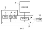
圖1是根據本發明的範例實施例所繪示的主機系統、記憶體儲存裝置及輸入/輸出(I/O)裝置的示意圖。圖2是根據本發明的範例實施例所繪示的主機系統、記憶體儲存裝置及I/O裝置的示意圖。Fig. 1 is a schematic diagram of a host system, a memory storage device, and an input/output (I/O) device according to an exemplary embodiment of the present invention. Fig. 2 is a schematic diagram of a host system, a memory storage device, and an I/O device according to an exemplary embodiment of the present invention.
請參照圖1與圖2,主機系統11可包括處理器111、隨機存取記憶體(random access memory, RAM)112、唯讀記憶體(read only memory, ROM)113及資料傳輸介面114。處理器111、隨機存取記憶體112、唯讀記憶體113及資料傳輸介面114可耦接至系統匯流排(system bus)110。1 and 2 , the
在一範例實施例中,主機系統11可透過資料傳輸介面114與記憶體儲存裝置10耦接。例如,主機系統11可經由資料傳輸介面114將資料儲存至記憶體儲存裝置10或從記憶體儲存裝置10中讀取資料。此外,主機系統11可透過系統匯流排110與I/O裝置12耦接。例如,主機系統11可經由系統匯流排110將輸出訊號傳送至I/O裝置12或從I/O裝置12接收輸入訊號。In an exemplary embodiment, the
在一範例實施例中,處理器111、隨機存取記憶體112、唯讀記憶體113及資料傳輸介面114可設置在主機系統11的主機板20上。資料傳輸介面114的數目可以是一或多個。透過資料傳輸介面114,主機板20可以經由有線或無線方式耦接至記憶體儲存裝置10。In an exemplary embodiment, the
在一範例實施例中,記憶體儲存裝置10可例如是隨身碟201、記憶卡202、固態硬碟(Solid State Drive, SSD)203或無線記憶體儲存裝置204。無線記憶體儲存裝置204可例如是近距離無線通訊(Near Field Communication, NFC)記憶體儲存裝置、無線傳真(WiFi)記憶體儲存裝置、藍牙(Bluetooth)記憶體儲存裝置或低功耗藍牙記憶體儲存裝置(例如,iBeacon)等以各式無線通訊技術為基礎的記憶體儲存裝置。此外,主機板20也可以透過系統匯流排110耦接至全球定位系統(Global Positioning System, GPS)模組205、網路介面卡206、無線傳輸裝置207、鍵盤208、螢幕209、喇叭210等各式I/O裝置。例如,在一範例實施例中,主機板20可透過無線傳輸裝置207存取無線記憶體儲存裝置204。In an exemplary embodiment, the
在一範例實施例中,主機系統11為電腦系統。在一範例實施例中,主機系統11可為可實質地與記憶體儲存裝置配合以儲存資料的任意系統。在一範例實施例中,記憶體儲存裝置10與主機系統11可分別包括圖3的記憶體儲存裝置30與主機系統31。In an exemplary embodiment, the
圖3是根據本發明的範例實施例所繪示的主機系統與記憶體儲存裝置的示意圖。請參照圖3,記憶體儲存裝置30可與主機系統31搭配使用以儲存資料。例如,主機系統31可以是數位相機、攝影機、通訊裝置、音訊播放器、視訊播放器或平板電腦等系統。例如,記憶體儲存裝置30可為主機系統31所使用的安全數位(Secure Digital, SD)卡32、小型快閃(Compact Flash, CF)卡33或嵌入式儲存裝置34等各式非揮發性記憶體儲存裝置。嵌入式儲存裝置34包括嵌入式多媒體卡(embedded Multi Media Card, eMMC)341及/或嵌入式多晶片封裝(embedded Multi Chip Package, eMCP)儲存裝置342等各類型將記憶體模組直接耦接於主機系統的基板上的嵌入式儲存裝置。FIG. 3 is a schematic diagram of a host system and a memory storage device according to an exemplary embodiment of the present invention. Referring to FIG. 3 , a
圖4是根據本發明的範例實施例所繪示的記憶體儲存裝置的示意圖。請參照圖4,記憶體儲存裝置10包括連接介面單元41、記憶體控制電路單元42與可複寫式非揮發性記憶體模組43。FIG4 is a schematic diagram of a memory storage device according to an exemplary embodiment of the present invention. Referring to FIG4 , the
連接介面單元41用以將記憶體儲存裝置10耦接主機系統11。記憶體儲存裝置10可經由連接介面單元41與主機系統11通訊。在一範例實施例中,連接介面單元41是相容於高速周邊零件互連(Peripheral Component Interconnect Express, PCI Express)標準。在一範例實施例中,連接介面單元41亦可以是符合序列先進附件(Serial Advanced Technology Attachment, SATA)標準、並列先進附件(Parallel Advanced Technology Attachment, PATA)標準、電氣和電子工程師協會(Institute of Electrical and Electronic Engineers, IEEE)1394標準、通用序列匯流排(Universal Serial Bus, USB)標準、SD介面標準、超高速一代(Ultra High Speed-I, UHS-I)介面標準、超高速二代(Ultra High Speed-II, UHS-II)介面標準、記憶棒(Memory Stick, MS)介面標準、MCP介面標準、MMC介面標準、eMMC介面標準、通用快閃記憶體(Universal Flash Storage, UFS)介面標準、eMCP介面標準、CF介面標準、整合式驅動電子介面(Integrated Device Electronics, IDE)標準或其他適合的標準。連接介面單元41可與記憶體控制電路單元42封裝在一個晶片中,或者連接介面單元41是佈設於一包含記憶體控制電路單元42之晶片外。The
記憶體控制電路單元42耦接至連接介面單元41與可複寫式非揮發性記憶體模組43。記憶體控制電路單元42用以執行以硬體型式或韌體型式實作的多個邏輯閘或控制指令並且根據主機系統11的指令在可複寫式非揮發性記憶體模組43中進行資料的寫入、讀取與抹除等運作。The memory
可複寫式非揮發性記憶體模組43用以儲存主機系統11所寫入之資料。可複寫式非揮發性記憶體模組43可包括單階記憶胞(Single Level Cell, SLC)NAND型快閃記憶體模組(即,一個記憶胞中可儲存1個位元的快閃記憶體模組)、二階記憶胞(Multi Level Cell, MLC)NAND型快閃記憶體模組(即,一個記憶胞中可儲存2個位元的快閃記憶體模組)、三階記憶胞(Triple Level Cell, TLC)NAND型快閃記憶體模組(即,一個記憶胞中可儲存3個位元的快閃記憶體模組)、四階記憶胞(Quad Level Cell, QLC)NAND型快閃記憶體模組(即,一個記憶胞中可儲存4個位元的快閃記憶體模組)、其他快閃記憶體模組或其他具有相同特性的記憶體模組。The rewritable
可複寫式非揮發性記憶體模組43中的每一個記憶胞是以電壓(以下亦稱為臨界電壓)的改變來儲存一或多個位元。具體來說,每一個記憶胞的控制閘極(control gate)與通道之間有一個電荷捕捉層。透過施予一寫入電壓至控制閘極,可以改變電荷補捉層的電子量,進而改變記憶胞的臨界電壓。此改變記憶胞之臨界電壓的操作亦稱為“把資料寫入至記憶胞”或“程式化(programming)記憶胞”。隨著臨界電壓的改變,可複寫式非揮發性記憶體模組43中的每一個記憶胞具有多個儲存狀態。透過施予讀取電壓可以判斷一個記憶胞是屬於哪一個儲存狀態,藉此取得此記憶胞所儲存的一或多個位元。Each memory cell in the rewritable
在一範例實施例中,可複寫式非揮發性記憶體模組43的記憶胞可構成多個實體程式化單元,並且此些實體程式化單元可構成多個實體抹除單元。具體來說,同一條字元線上的記憶胞可組成一或多個實體程式化單元。若每一個記憶胞可儲存2個以上的位元,則同一條字元線上的實體程式化單元可至少可被分類為下實體程式化單元與上實體程式化單元。例如,一記憶胞的最低有效位元(Least Significant Bit, LSB)是屬於下實體程式化單元,並且一記憶胞的最高有效位元(Most Significant Bit, MSB)是屬於上實體程式化單元。一般來說,在MLC NAND型快閃記憶體中,下實體程式化單元的寫入速度會大於上實體程式化單元的寫入速度,及/或下實體程式化單元的可靠度是高於上實體程式化單元的可靠度。In an exemplary embodiment, the memory cells of the rewritable
在一範例實施例中,實體程式化單元為程式化的最小單元。即,實體程式化單元為寫入資料的最小單元。例如,實體程式化單元可為實體頁(page)或是實體扇(sector)。若實體程式化單元為實體頁,則此些實體程式化單元可包括資料位元區與冗餘(redundancy)位元區。資料位元區包含多個實體扇,用以儲存使用者資料,而冗餘位元區用以儲存系統資料(例如,錯誤更正碼等管理資料)。在一範例實施例中,資料位元區包含32個實體扇,且一個實體扇的大小為512位元組(byte, B)。然而,在其他範例實施例中,資料位元區中也可包含8個、16個或數目更多或更少的實體扇,並且每一個實體扇的大小也可以是更大或更小。另一方面,實體抹除單元為抹除之最小單位。亦即,每一實體抹除單元含有最小數目之一併被抹除之記憶胞。例如,實體抹除單元為實體區塊(block)。In an exemplary embodiment, the physical programming unit is the smallest unit of programming. That is, the physical programming unit is the smallest unit for writing data. For example, the physical programming unit may be a physical page or a physical sector. If the physical programming unit is a physical page, these physical programming units may include a data bit area and a redundancy bit area. The data bit area includes a plurality of physical sectors for storing user data, and the redundancy bit area is used to store system data (for example, management data such as error correction codes). In an exemplary embodiment, the data byte area includes 32 physical sectors, and the size of a physical sector is 512 bytes (byte, B). However, in other exemplary embodiments, the data bit area may also include 8, 16, or more or fewer physical sectors, and the size of each physical sector may also be larger or smaller. On the other hand, the physical erase unit is the minimum unit of erasure. That is, each physical erase unit contains a minimum number of memory cells that are erased. For example, the physical erase unit is a physical block.
圖5是根據本發明的範例實施例所繪示的記憶體控制電路單元的示意圖。請參照圖5,記憶體控制電路單元42包括記憶體管理電路51、主機介面52及記憶體介面53。FIG5 is a schematic diagram of a memory control circuit unit according to an exemplary embodiment of the present invention. Referring to FIG5 , the memory
記憶體管理電路51用以控制記憶體控制電路單元42的整體運作。具體來說,記憶體管理電路51具有多個控制指令,並且在記憶體儲存裝置10運作時,此些控制指令會被執行以進行資料的寫入、讀取與抹除等運作。以下說明記憶體管理電路51的操作時,等同於說明記憶體控制電路單元42的操作。The
在一範例實施例中,記憶體管理電路51的控制指令是以韌體型式來實作。例如,記憶體管理電路51具有微處理器單元(未繪示)與唯讀記憶體(未繪示),並且此些控制指令是被燒錄至此唯讀記憶體中。當記憶體儲存裝置10運作時,此些控制指令會由微處理器單元來執行以進行資料的寫入、讀取與抹除等運作。In an exemplary embodiment, the control instructions of the
在一範例實施例中,記憶體管理電路51的控制指令亦可以程式碼型式儲存於可複寫式非揮發性記憶體模組43的特定區域(例如,記憶體模組中專用於存放系統資料的系統區)中。此外,記憶體管理電路51具有微處理器單元(未繪示)、唯讀記憶體(未繪示)及隨機存取記憶體(未繪示)。特別是,此唯讀記憶體具有開機碼(boot code),並且當記憶體控制電路單元42被致能時,微處理器單元會先執行此開機碼來將儲存於可複寫式非揮發性記憶體模組43中之控制指令載入至記憶體管理電路51的隨機存取記憶體中。之後,微處理器單元會運轉此些控制指令以進行資料的寫入、讀取與抹除等運作。In an exemplary embodiment, the control instructions of the
在一範例實施例中,記憶體管理電路51的控制指令亦可以一硬體型式來實作。例如,記憶體管理電路51包括微控制器、記憶胞管理電路、記憶體寫入電路、記憶體讀取電路、記憶體抹除電路與資料處理電路。記憶胞管理電路、記憶體寫入電路、記憶體讀取電路、記憶體抹除電路與資料處理電路是耦接至微控制器。記憶胞管理電路用以管理可複寫式非揮發性記憶體模組43的記憶胞或記憶胞群組。記憶體寫入電路用以對可複寫式非揮發性記憶體模組43下達寫入指令序列以將資料寫入至可複寫式非揮發性記憶體模組43中。記憶體讀取電路用以對可複寫式非揮發性記憶體模組43下達讀取指令序列以從可複寫式非揮發性記憶體模組43中讀取資料。記憶體抹除電路用以對可複寫式非揮發性記憶體模組43下達抹除指令序列以將資料從可複寫式非揮發性記憶體模組43中抹除。資料處理電路用以處理欲寫入至可複寫式非揮發性記憶體模組43的資料以及從可複寫式非揮發性記憶體模組43中讀取的資料。寫入指令序列、讀取指令序列及抹除指令序列可各別包括一或多個程式碼或指令碼並且用以指示可複寫式非揮發性記憶體模組43執行相對應的寫入、讀取及抹除等操作。在一範例實施例中,記憶體管理電路51還可以下達其他類型的指令序列給可複寫式非揮發性記憶體模組43以指示執行相對應的操作。In an exemplary embodiment, the control instructions of the
主機介面52是耦接至記憶體管理電路51。記憶體管理電路51可透過主機介面52與主機系統11通訊。主機介面52可用以接收與識別主機系統11所傳送的指令與資料。例如,主機系統11所傳送的指令與資料可透過主機介面52來傳送至記憶體管理電路51。此外,記憶體管理電路51可透過主機介面52將資料傳送至主機系統11。在本範例實施例中,主機介面52是相容於PCI Express標準。然而,必須瞭解的是本發明不限於此,主機介面52亦可以是相容於SATA標準、PATA標準、IEEE 1394標準、USB標準、SD標準、UHS-I標準、UHS-II標準、MS標準、MMC標準、eMMC標準、UFS標準、CF標準、IDE標準或其他適合的資料傳輸標準。The
記憶體介面53是耦接至記憶體管理電路51並且用以存取可複寫式非揮發性記憶體模組43。例如,記憶體管理電路51可透過記憶體介面53存取可複寫式非揮發性記憶體模組43。也就是說,欲寫入至可複寫式非揮發性記憶體模組43的資料會經由記憶體介面53轉換為可複寫式非揮發性記憶體模組43所能接受的格式。具體來說,若記憶體管理電路51要存取可複寫式非揮發性記憶體模組43,記憶體介面53會傳送對應的指令序列。例如,這些指令序列可包括指示寫入資料的寫入指令序列、指示讀取資料的讀取指令序列、指示抹除資料的抹除指令序列、以及用以指示各種記憶體操作(例如,改變讀取電壓準位等)的相對應的指令序列。這些指令序列例如是由記憶體管理電路51產生並且透過記憶體介面53傳送至可複寫式非揮發性記憶體模組43。這些指令序列可包括一或多個訊號,或是在匯流排上的資料。這些訊號或資料可包括指令碼或程式碼。例如,在讀取指令序列中,會包括讀取的辨識碼、記憶體位址等資訊。The
在一範例實施例中,記憶體控制電路單元42還包括錯誤檢查與校正電路54、緩衝記憶體55及電源管理電路56。In an exemplary embodiment, the memory
錯誤檢查與校正電路54是耦接至記憶體管理電路51並且用以執行錯誤檢查與校正操作以確保資料的正確性。具體來說,當記憶體管理電路51從主機系統11中接收到寫入指令時,錯誤檢查與校正電路54會為對應此寫入指令的資料產生對應的錯誤更正碼(error correcting code, ECC)及/或錯誤檢查碼(error detecting code,EDC),並且記憶體管理電路51會將對應此寫入指令的資料與對應的錯誤更正碼及/或錯誤檢查碼寫入至可複寫式非揮發性記憶體模組43中。之後,當記憶體管理電路51從可複寫式非揮發性記憶體模組43中讀取資料時會同時讀取此資料對應的錯誤更正碼及/或錯誤檢查碼,並且錯誤檢查與校正電路54會依據此錯誤更正碼及/或錯誤檢查碼對所讀取的資料執行錯誤檢查與校正操作。例如,錯誤檢查與校正電路54可支援低密度奇偶檢查碼(Low Density Parity Check code, LDPC code)或BCH等各式編/解碼演算法。The error checking and
緩衝記憶體55是耦接至記憶體管理電路51並且用以暫存資料。電源管理電路56是耦接至記憶體管理電路51並且用以控制記憶體儲存裝置10的電源。The
在一範例實施例中,圖4的可複寫式非揮發性記憶體模組43可包括快閃記憶體模組。在一範例實施例中,圖4的記憶體控制電路單元42可包括快閃記憶體控制器。在一範例實施例中,圖5的記憶體管理電路51可包括快閃記憶體管理電路。In an exemplary embodiment, the rewritable
可複寫式非揮發性記憶體模組43可包括多個實體單元。在一範例實施例中,一個實體單元是指一個實體位址或一個實體程式化單元。在一範例實施例中,一個實體單元亦可以是由多個連續或不連續的實體位址組成。在一範例實施例中,一個實體單元亦可以是指一個虛擬區塊(VB)。一個虛擬區塊可包括多個實體位址或多個實體程式化單元。The rewritable
在一範例實施例中,記憶體管理電路51可配置邏輯單元以映射實體單元。在一範例實施例中,每一個邏輯單元對應一個邏輯位址。例如,一個邏輯位址可包括一或多個邏輯區塊位址(Logical Block Address, LBA)或其他的邏輯管理單元。在一範例實施例中,一個邏輯單元也可對應一個邏輯程式化單元或者由多個連續或不連續的邏輯位址組成。In an exemplary embodiment, the
須注意的是,一個邏輯單元可被映射至一或多個實體單元。若某一實體單元當前有被某一邏輯單元映射,則表示此實體單元當前儲存的資料包括有效資料。反之,若某一實體單元當前未被任一邏輯單元映射,則表示此實體單元當前儲存的資料為無效資料。此外,描述邏輯單元與實體單元之間的映射關係的邏輯至實體映射資訊可記載於邏輯至實體映射表中。爾後,記憶體管理電路51可根據此邏輯至實體映射表中的資訊來存取可複寫式非揮發性記憶體模組43。It should be noted that a logic unit can be mapped to one or more physical units. If a physical unit is currently mapped by a logic unit, it means that the data currently stored in this physical unit includes valid data. On the contrary, if a physical unit is not currently mapped by any logic unit, it means that the data currently stored in this physical unit is invalid data. In addition, the logic-to-physical mapping information describing the mapping relationship between the logic unit and the physical unit can be recorded in the logic-to-physical mapping table. Thereafter, the
圖6是根據本發明的範例實施例所繪示的管理可複寫式非揮發性記憶體模組的示意圖。請參照圖6,假設可複寫式非揮發性記憶體模組43包括實體單元610(0)~610(B)。在啟動(例如初次啟動)記憶體儲存裝置10時,記憶體管理電路51可執行一個初始化操作,以對記憶體儲存裝置10內部的管理資訊進行初始化設定。FIG6 is a schematic diagram of managing a rewritable non-volatile memory module according to an exemplary embodiment of the present invention. Referring to FIG6 , it is assumed that the rewritable
在初始化操作中,記憶體管理電路51可將實體單元610(0)~610(A)分類為第一類實體單元61並將實體單元610(A+1)~610(B)分類為第二類實體單元62。根據分類結果,記憶體管理電路51可將屬於第一類實體單元61的實體單元610(0)~610(A)設定為採用一個特定的操作模式(亦稱為第一操作模式)並將屬於第二類實體單元62的實體單元610(A+1)~610(B)設定為採用另一種操作模式(亦稱為第二操作模式)。第一操作模式不同於第二操作模式。在第一操作模式下,一個實體單元可基於一個特定的程式化模式(亦稱為第一程式化模式)來程式化。此外,在第二操作模式下,一個實體單元可基於另一個特定的程式化模式(亦稱為第二程式化模式)來程式化。In the initialization operation, the
須注意的是,在初始化操作中,被分類為第一類實體單元61的實體單元(例如實體單元610(0)~610(A))的總數及被分類為第二類實體單元62的實體單元(例如實體單元610(A+1)~610(B))的總數皆為預設數目。此外,可複寫式非揮發性記憶體模組43還可包括其他的實體單元,本發明不加以限制。It should be noted that, in the initialization operation, the total number of physical units classified as the first type of physical units 61 (e.g., physical units 610(0) to 610(A)) and the total number of physical units classified as the second type of physical units 62 (e.g., physical units 610(A+1) to 610(B)) are both preset numbers. In addition, the rewritable
在一範例實施例中,在基於第一程式化模式來程式化的一個實體單元中,一個記憶胞可用以儲存m個位元。在一範例實施例中,在基於第二程式化模式來程式化的一個實體單元中,一個記憶胞可用以儲存n個位元,且m大於n。例如,n可為“1”,且m可為“2”、“3”或“4”,且本發明不限於此。在一範例實施例中,n與m亦可為其他正整數,只要滿足m大於n之規範即可。In an exemplary embodiment, in a physical unit programmed based on the first programming mode, a memory cell can be used to store m bits. In an exemplary embodiment, in a physical unit programmed based on the second programming mode, a memory cell can be used to store n bits, and m is greater than n. For example, n can be "1", and m can be "2", "3" or "4", and the present invention is not limited thereto. In an exemplary embodiment, n and m can also be other positive integers, as long as the specification that m is greater than n is satisfied.
在一範例實施例中,第一程式化模式是指MLC程式化模式、TLC程式化模式、QLC程式化模式或類似模式。例如,基於MLC程式化模式程式化的一個記憶胞可儲存2個位元,基於TLC程式化模式程式化的一個記憶胞可儲存3個位元,且基於QLC程式化模式程式化的一個記憶胞可儲存4個位元。In an exemplary embodiment, the first programming mode refers to an MLC programming mode, a TLC programming mode, a QLC programming mode, or a similar mode. For example, a memory cell programmed based on the MLC programming mode can store 2 bits, a memory cell programmed based on the TLC programming mode can store 3 bits, and a memory cell programmed based on the QLC programming mode can store 4 bits.
在一範例實施例中,第二程式化模式是指SLC程式化模式、虛擬(pseudo)SLC程式化模式、下實體程式化(lower physical programming)模式、混合程式化(mixture programming)模式及少層記憶胞(less layer memory cell)模式的其中之一。在SLC程式化模式與虛擬SLC程式化模式中,一個記憶胞只儲存一個位元的資料。在下實體程式化模式中,只有下實體程式化單元會被程式化,而此下實體程式化單元所對應之上實體程式化單元可不被程式化。在混合程式化模式中,有效資料(或真實資料)會被程式化於下實體程式化單元中,而同時虛擬資料(dummy data)會被程式化至儲存有效資料之下實體程式化單元所對應的上實體程式化單元中。在少層記憶胞模式中,只有一部分的實體程式化單元會被程式化以儲存有效資料。例如,基於SLC程式化模式、虛擬SLC程式化模式、下實體程式化模式、混合程式化模式及少層記憶胞模式程式化的一個記憶胞可儲存1個位元。然而,基於第一程式化模式與第二程式化模式程式化的一個記憶胞所儲存的位元之總數亦可根據實務需求調整,本發明不加以限制。In an exemplary embodiment, the second programming mode refers to one of an SLC programming mode, a pseudo SLC programming mode, a lower physical programming mode, a mixture programming mode, and a less layer memory cell mode. In the SLC programming mode and the pseudo SLC programming mode, a memory cell stores only one bit of data. In the lower physical programming mode, only the lower physical programming unit is programmed, and the upper physical programming unit corresponding to the lower physical programming unit may not be programmed. In the hybrid programming mode, valid data (or real data) will be programmed in the lower physical programming unit, and at the same time, dummy data will be programmed into the upper physical programming unit corresponding to the lower physical programming unit storing the valid data. In the few-layer memory cell mode, only a portion of the physical programming units will be programmed to store valid data. For example, a memory cell programmed based on the SLC programming mode, the virtual SLC programming mode, the lower physical programming mode, the hybrid programming mode, and the few-layer memory cell mode can store 1 bit. However, the total number of bits stored in a memory cell programmed based on the first programming mode and the second programming mode can also be adjusted according to practical needs, and the present invention is not limited thereto.
在一範例實施例中,透過第二程式化模式執行的主機寫入操作的寫入效能高於透過第一程式化模式執行的主機寫入操作的寫入效能。例如,在針對資料量相同的資料X與資料Y分別執行主機寫入的情況下,透過第二程式化模式將資料X寫入至屬於第二類實體單元62的至少一實體單元中的寫入效能,可高於透過第一程式化模式將資料Y寫入至屬於第一類實體單元61的至少一實體單元中的寫入效能。在一範例實施例中,基於第二程式化模式所儲存的資料的可靠度亦可高於基於第一程式化模式所儲存的資料的可靠度。In an exemplary embodiment, the write performance of the host write operation executed through the second programming mode is higher than the write performance of the host write operation executed through the first programming mode. For example, when the host write is performed for data X and data Y of the same data amount, the write performance of writing data X to at least one physical unit belonging to the second type of
在一範例實施例中,採用第一操作模式的實體單元只能基於第一程式化模式(例如TLC程式化模式)來程式化,以儲存資料。然而,採用第二操作模式的實體單元可基於第一程式化模式(例如TLC程式化模式)與第二程式化模式(例如SLC程式化模式)的其中之一來程式化,以儲存資料。例如,在某一時間點(例如需要直接儲存來自主機系統11的資料時),屬於第二類實體單元62的至少一實體單元可被設定為基於第二程式化模式來程式化,以提高主機寫入的寫入效能。此外,在另一時間點(例如執行可複寫式非揮發性記憶體模組43內部的資料搬移時),屬於第二類實體單元62的至少一實體單元可被設定為基於第一程式化模式來程式化,以加大可複寫式非揮發性記憶體模組43的資料儲存量。In an exemplary embodiment, a physical unit using the first operation mode can only be programmed based on the first programming mode (e.g., TLC programming mode) to store data. However, a physical unit using the second operation mode can be programmed based on one of the first programming mode (e.g., TLC programming mode) and the second programming mode (e.g., SLC programming mode) to store data. For example, at a certain point in time (e.g., when data from the
在一範例實施例中,假設可複寫式非揮發性記憶體模組43中的至少一實體單元(亦稱為第一實體單元)在初始化操作中被設定為採用第一操作模式(即屬於第一類實體單元61)。例如,第一實體單元可為圖6中的實體單元610(0)~610(A)中的一或多個實體單元。藉此,在第一操作模式下,第一實體單元可基於第一程式化模式進行程式化。在一範例實施例中,第一操作模式可視為第一實體單元的預設操作模式。In an exemplary embodiment, it is assumed that at least one physical unit (also referred to as a first physical unit) in the rewritable
在執行初始化操作後,記憶體管理電路51可從主機系統11接收多個指令。所述多個指令包括第一指令與第二指令。第一指令指示將資料(亦稱為第一資料)儲存至特定邏輯單元(亦稱為第一邏輯單元)。例如,第一指令可包括寫入指令。根據第一指令,記憶體管理電路51可指示可複寫式非揮發性記憶體模組43基於第一程式化模式或第二程式化模式將第一資料儲存至第一邏輯單元所映射的至少一實體單元中。第二指令指示將儲存於特定邏輯單元(亦稱為第二邏輯單元)的資料(亦稱為第二資料)標記為無效資料。例如,第二指令可包括Trim指令。根據第二指令,記憶體管理電路51可將儲存於第二邏輯單元的第二資料標記為無效資料。爾後,來自主機系統11的新資料(即更多的第一資料)可被儲存至第二邏輯單元。After performing the initialization operation, the
在一範例實施例中,在第一實體單元被設定為採用第一操作模式的情況下,響應於特定條件(亦稱為目標條件)被滿足,記憶體管理電路51可根據第二指令改變第一實體單元的操作模式,例如將第一實體單元設定為採用第二操作模式(等同於將第一實體單元分類為第二類實體單元62)。藉此,在第二操作模式下,第一實體單元可基於第二程式化模式進行程式化。在一範例實施例中,透過將第一實體單元切換為採用第二操作模式,可增加第二類實體單元62的總數、減少第二類實體單元62被用盡的機率及/或延緩第二類實體單元62被用盡的時間點,從而提高主機寫入的寫入效能。In an exemplary embodiment, when the first physical unit is set to adopt the first operation mode, in response to a specific condition (also referred to as a target condition) being met, the
在一範例實施例中,在第一實體單元被設定為採用第一操作模式且目標條件已被滿足的情況下,記憶體管理電路51可判斷所接收的第二指令的總數是否達到一個臨界值(亦稱為第一臨界值)及/或第二資料的總資料量是否達到一個臨界值(亦稱為第二臨界值)。例如,第一臨界值可為100,第二臨界值可為4GB,且本發明不限於此。例如,第二資料的總資料量可正相關於所接收到的第二指令的總數。例如,在接收到更多來自主機系統11的第二指令後,第二指令的總數及第二資料的總資料量皆可對應增加。In an exemplary embodiment, when the first physical unit is set to adopt the first operation mode and the target condition has been met, the
在一範例實施例中,在第一實體單元被設定為採用第一操作模式且目標條件已被滿足的情況下,響應於第二指令的總數達到第一臨界值及/或第二資料的總資料量達到第二臨界值,改變第一實體單元的操作模式之操作可被觸發。此時,記憶體管理電路51可將第一實體單元設定為採用第二操作模式。此外,在一範例實施例中,若第二指令的總數未達第一臨界值及/或第二資料的總資料量未達第二臨界值,則改變第一實體單元的操作模式之操作可不被觸發。因此,記憶體管理電路51可不改變第一實體單元的操作模式(等同於將第一實體單元維持於採用第一操作模式)。In an exemplary embodiment, when the first physical unit is set to adopt the first operating mode and the target condition has been met, in response to the total number of second instructions reaching the first critical value and/or the total amount of second data reaching the second critical value, the operation of changing the operating mode of the first physical unit may be triggered. At this time, the
在一範例實施例中,在第一實體單元被設定為採用第一操作模式的情況下,記憶體管理電路51可判斷第一資料的總資料量是否達到一個臨界值(亦稱為第三臨界值)及/或採用第二操作模式儲存的資料(亦稱為第三資料)的總資料量是否達到一個臨界值(亦稱為第四臨界值)。例如,第三臨界值可為可複寫式非揮發性記憶體模組43的總容量的75%,第四臨界值可為6GB,且本發明不限於此。例如,第一資料的總資料量可正相關於所接收到的第一指令的總數。例如,在接收到更多來自主機系統11的第一指令後,所儲存的第一資料的總資料量可對應增加。此外,記憶體管理電路51可持續監控當前屬於第二類實體單元62的實體單元的使用狀況,以獲得當前採用第二操作模式儲存的第三資料的總資料量。例如,記憶體管理電路51可根據當前儲存於第二類實體單元62中的有效資料的總資料量來獲得第三資料的總資料量。In an exemplary embodiment, when the first physical unit is set to adopt the first operating mode, the
在一範例實施例中,在第一實體單元被設定為採用第一操作模式的情況下,響應於第一資料的總資料量達到第三臨界值及/或第三資料的總資料量達到第四臨界值,記憶體管理電路51可判定所述目標條件被滿足。此外,在一範例實施例中,若第一資料的總資料量未達第三臨界值及/或第三資料的總資料量未達第四臨界值,則記憶體管理電路51可判定所述目標條件未被滿足。In an exemplary embodiment, when the first physical unit is configured to adopt the first operation mode, in response to the total data amount of the first data reaching the third critical value and/or the total data amount of the third data reaching the fourth critical value, the
在一範例實施例中,在判斷目標條件是否被滿足的操作中,記憶體管理電路51可先判斷第一資料的總資料量是否達到第三臨界值。響應於第一資料的總資料量達到第三臨界值,記憶體管理電路51可接續判斷採用第二操作模式儲存的第三資料的總資料量是否達到第四臨界值。或者,在一範例實施例中,在判斷目標條件是否被滿足的操作中,記憶體管理電路51亦可先判斷採用第二操作模式儲存的第三資料的總資料量是否達到第四臨界值。響應於第三資料的總資料量達到第四臨界值,記憶體管理電路51可接續判斷第一資料的總資料量是否達到第三臨界值。然而,若第一資料的總資料量未達第三臨界值或第三資料的總資料量未達第四臨界值,則記憶體管理電路51可判定所述目標條件未被滿足。In an exemplary embodiment, in the operation of determining whether the target condition is satisfied, the
在一範例實施例中,在將第一實體單元設定為採用第二操作模式後,在一個預設的時間範圍內,記憶體管理電路51可將第一實體單元維持於採用第二操作模式。然而,在離開此時間範圍後,記憶體管理電路51可將第一實體單元回復為採用第一操作模式。例如,在將第一實體單元設定為採用第二操作模式後,記憶體管理電路51可啟動一個計數器。記憶體管理電路51可根據此計數器的計數值來判斷是否已離開此時間範圍。In an exemplary embodiment, after the first physical unit is set to adopt the second operation mode, the
換言之,在一範例實施例中,在第一實體單元被設定為採用第一操作模式的情況下,響應於目標條件被滿足,記憶體管理電路51可暫時將第一實體單元設定為採用第二操作模式,而非永久地將第一實體單元切換為採用第二操作模式。藉此,可在短時間內嘗試提高主機寫入的寫入效能。此外,透過短暫地改變第一實體單元的操作模式,也可盡可能地減少對實體單元的預設管理機制的干擾,進而增加系統的操作穩定性。In other words, in an exemplary embodiment, when the first physical unit is set to adopt the first operation mode, in response to the target condition being met, the
圖7是根據本發明的範例實施例所繪示的改變第一實體單元的操作模式的示意圖。請參照圖7,假設在第一實體單元被設定為採用第一操作模式的情況下,在時間點T(0),記憶體管理電路51將第一實體單元設定為採用第二操作模式。在時間點T(0)至T(1)之間(即預設的時間範圍內),記憶體管理電路51可將第一實體單元維持於採用第二操作模式。接著,在時間點T(1)後(即離開所述預設的時間範圍後),記憶體管理電路51可將第一實體單元回復為採用第一操作模式。例如,所述預設的時間範圍可為10秒,且本發明不限於此。FIG. 7 is a schematic diagram of changing the operation mode of the first entity unit according to an exemplary embodiment of the present invention. Referring to FIG. 7 , assuming that the first entity unit is set to adopt the first operation mode, at time point T(0), the
在一範例實施例中,在所述預設的時間範圍內,記憶體管理電路51還可禁止或延遲執行資料整併操作。此資料整併操作可透過搬移(包含複製)有效資料來釋放閒置實體單元。例如,此資料整併操作可包括垃圾回收(Garbage Collection, GC)操作。例如,閒置實體單元是指沒有儲存有效資料的實體單元。例如,在資料整併操作中,記憶體管理電路51可從作為來源單元的實體單元中收集有效資料並將所收集的有效資料集中儲存到作為目標單元的實體單元中。然後,作為來源單元的實體單元可被標記為閒置實體單元並且可被抹除。此外,在離開所述預設的時間範圍後,記憶體管理電路51可解除對資料整併操作的管制。例如,在離開所述預設的時間範圍後,記憶體管理電路51可允許執行先前被禁止或延遲的資料整併操作。在一範例實施例中,透過在所述預設的時間範圍內增加可基於第二程式化模式來程式化的實體單元並禁止或延遲執行所述資料整併操作,可更進一步提高主機寫入的寫入效能。In an exemplary embodiment, within the preset time range, the
圖8是根據本發明的範例實施例所繪示的記憶體管理方法的流程圖。請參照圖8,在步驟S801中,在初始化操作中,將第一實體單元設定為採用第一操作模式,其中在第一操作模式下,第一實體單元是基於第一程式化模式來程式化。在步驟S802中,從主機系統接收多個指令,其中所述多個指令包括第一指令與第二指令,第一指令指示將第一資料儲存至第一邏輯單元,且第二指令指示將儲存於第二邏輯單元的第二資料標記為無效資料。在步驟S803中,判斷目標條件是否被滿足。若目標條件被滿足,在步驟S804中,根據第二指令,將第一實體單元設定為採用第二操作模式,其中在第二操作模式下,第一實體單元可基於第二程式化模式來程式化,且第一程式化模式不同於第二程式化模式。此外,若目標條件未被滿足,則步驟S802可重複執行。FIG8 is a flow chart of a memory management method according to an exemplary embodiment of the present invention. Referring to FIG8, in step S801, in an initialization operation, a first physical unit is set to adopt a first operation mode, wherein in the first operation mode, the first physical unit is programmed based on a first programming mode. In step S802, a plurality of instructions are received from a host system, wherein the plurality of instructions include a first instruction and a second instruction, the first instruction instructing to store first data in a first logic unit, and the second instruction instructing to mark second data stored in a second logic unit as invalid data. In step S803, it is determined whether a target condition is satisfied. If the target condition is met, in step S804, according to the second instruction, the first physical unit is set to adopt a second operation mode, wherein in the second operation mode, the first physical unit can be programmed based on a second programming mode, and the first programming mode is different from the second programming mode. In addition, if the target condition is not met, step S802 can be repeatedly executed.
圖9是根據本發明的範例實施例所繪示的記憶體管理方法的流程圖。請參照圖9,在步驟S901中,在初始化操作中,將第一實體單元設定為採用第一操作模式。在步驟S902中,從主機系統接收多個指令,其中所述多個指令包括第一指令與第二指令,第一指令指示將第一資料儲存至第一邏輯單元,且第二指令指示將儲存於第二邏輯單元的第二資料標記為無效資料。在步驟S903中,判斷第一資料的總資料量是否達到臨界值(即第三臨界值)。若第一資料的總資料量達到第三臨界值,在步驟S904中,判斷採用第二操作模式儲存的第三資料的總資料量是否達到臨界值(即第四臨界值)。若第三資料的總資料量達到第四臨界值,在步驟S905中,判斷第二指令的總數是否達到臨界值(即第一臨界值)或第二資料的總資料量是否達到臨界值(即第二臨界值)。若第二指令的總數達到第一臨界值或第二資料的總資料量達到第二臨界值,在步驟S906中,將第一實體單元設定為採用第二操作模式。此外,若步驟S903、S904及S905的判斷結果為否,則步驟S902可重複執行。FIG. 9 is a flow chart of a memory management method according to an exemplary embodiment of the present invention. Referring to FIG. 9 , in step S901, in an initialization operation, a first physical unit is set to adopt a first operation mode. In step S902, a plurality of instructions are received from a host system, wherein the plurality of instructions include a first instruction and a second instruction, the first instruction instructing to store the first data in the first logic unit, and the second instruction instructing to mark the second data stored in the second logic unit as invalid data. In step S903, it is determined whether the total data amount of the first data reaches a critical value (i.e., a third critical value). If the total amount of the first data reaches the third critical value, in step S904, it is determined whether the total amount of the third data stored in the second operation mode reaches the critical value (i.e., the fourth critical value). If the total amount of the third data reaches the fourth critical value, in step S905, it is determined whether the total number of the second instructions reaches the critical value (i.e., the first critical value) or the total amount of the second data reaches the critical value (i.e., the second critical value). If the total number of the second instructions reaches the first critical value or the total amount of the second data reaches the second critical value, in step S906, the first entity unit is set to adopt the second operation mode. In addition, if the judgment results of steps S903, S904 and S905 are no, step S902 can be repeatedly executed.
圖10是根據本發明的範例實施例所繪示的記憶體管理方法的流程圖。請參照圖10,在第一實體單元被設定為採用第一操作模式的情況下,在步驟S1001中,將第一實體單元設定為採用第二操作模式。在步驟S1002中,判斷是否離開預設的時間範圍。若已離開預設的時間範圍,在步驟S1003中,將第一實體單元回復為採用第一操作模式。此外,若尚未離開預設的時間範圍,則可將第一實體單元維持為採用第二操作模式。FIG. 10 is a flow chart of a memory management method according to an exemplary embodiment of the present invention. Referring to FIG. 10 , when the first entity unit is set to adopt the first operation mode, in step S1001, the first entity unit is set to adopt the second operation mode. In step S1002, it is determined whether the preset time range has been left. If the preset time range has been left, in step S1003, the first entity unit is restored to adopt the first operation mode. In addition, if the preset time range has not been left, the first entity unit can be maintained in the second operation mode.
然而,圖8至圖10中各步驟已詳細說明如上,在此便不再贅述。值得注意的是,圖8至圖10中各步驟可以實作為多個程式碼或是電路,本發明不加以限制。此外,圖8至圖10的方法可以搭配以上範例實施例使用,也可以單獨使用,本發明不加以限制。However, each step in FIG. 8 to FIG. 10 has been described in detail above, and will not be repeated here. It is worth noting that each step in FIG. 8 to FIG. 10 can be implemented as multiple program codes or circuits, and the present invention is not limited thereto. In addition, the method of FIG. 8 to FIG. 10 can be used in conjunction with the above exemplary embodiments, or can be used alone, and the present invention is not limited thereto.
綜上所述,本發明的範例實施例提出的記憶體管理方法、記憶體儲存裝置及記憶體控制電路單元,可在特定時間點或滿足特定條件時,改變可複寫式非揮發性記憶體模組中的至少部分實體單元(即第一實體單元)的操作模式,例如將第一實體單元的操作模式從第一操作模式改為第二操作模式,以提升主機寫入的寫入效能。此外,透過暫時而非永久地改變第一實體單元的操作模式,例如在經過一段時間後將第一實體單元的操作模式回復為第一操作模式(即第一實體單元的預設操作模式),可減少對實體單元的預設管理機制的干擾,進而增加系統的操作穩定性。In summary, the memory management method, memory storage device, and memory control circuit unit proposed in the exemplary embodiment of the present invention can change the operation mode of at least part of the physical units (i.e., the first physical unit) in the rewritable non-volatile memory module at a specific time point or when specific conditions are met, such as changing the operation mode of the first physical unit from the first operation mode to the second operation mode to improve the write performance of the host write. In addition, by temporarily rather than permanently changing the operation mode of the first physical unit, such as restoring the operation mode of the first physical unit to the first operation mode (i.e., the default operation mode of the first physical unit) after a period of time, the interference with the default management mechanism of the physical unit can be reduced, thereby increasing the operational stability of the system.
雖然本發明已以實施例揭露如上,然其並非用以限定本發明,任何所屬技術領域中具有通常知識者,在不脫離本發明的精神和範圍內,當可作些許的更動與潤飾,故本發明的保護範圍當視後附的申請專利範圍所界定者為準。Although the present invention has been disclosed as above by the embodiments, they are not intended to limit the present invention. Any person with ordinary knowledge in the relevant technical field can make some changes and modifications without departing from the spirit and scope of the present invention. Therefore, the protection scope of the present invention shall be defined by the scope of the attached patent application.
10,30:記憶體儲存裝置 11,31:主機系統 110:系統匯流排 111:處理器 112:隨機存取記憶體 113:唯讀記憶體 114:資料傳輸介面 12:輸入/輸出(I/O)裝置 20:主機板 201:隨身碟 202:記憶卡 203:固態硬碟 204:無線記憶體儲存裝置 205:全球定位系統模組 206:網路介面卡 207:無線傳輸裝置 208:鍵盤 209:螢幕 210:喇叭 32:SD卡 33:CF卡 34:嵌入式儲存裝置 341:嵌入式多媒體卡 342:嵌入式多晶片封裝儲存裝置 41:連接介面單元 42:記憶體控制電路單元 43:可複寫式非揮發性記憶體模組 51:記憶體管理電路 52:主機介面 53:記憶體介面 54:錯誤檢查與校正電路 55:緩衝記憶體 56:電源管理電路 61:第一類實體單元 62:第二類實體單元 610(0)~610(B):實體單元 T(0),T(1):時間點 S801:步驟(在初始化操作中,將第一實體單元設定為採用第一操作模式,其中在第一操作模式下,第一實體單元是基於第一程式化模式來程式化) S802:步驟(從主機系統接收多個指令,其中所述多個指令包括第一指令與第二指令,第一指令指示將第一資料儲存至第一邏輯單元,且第二指令指示將儲存於第二邏輯單元的第二資料標記為無效資料) S803:步驟(目標條件被滿足?) S804:步驟(根據第二指令,將第一實體單元設定為採用第二操作模式,其中在第二操作模式下,第一實體單元可基於第二程式化模式來程式化,且第一程式化模式不同於第二程式化模式) S901:步驟(在初始化操作中,將第一實體單元設定為採用第一操作模式) S902:步驟(從主機系統接收多個指令,其中所述多個指令包括第一指令與第二指令,第一指令指示將第一資料儲存至第一邏輯單元,且第二指令指示將儲存於第二邏輯單元的第二資料標記為無效資料) S903:步驟(第一資料的總資料量達到臨界值?) S904:步驟(採用第二操作模式儲存的第三資料的總資料量達到臨界值?) S905:步驟(第二指令的總數達到臨界值或第二資料的總資料量達到臨界值?) S906:步驟(將第一實體單元設定為採用第二操作模式) S1001:步驟(將第一實體單元設定為採用第二操作模式) S1002:步驟(離開時間範圍?) S1003:步驟(將第一實體單元回復為採用第一操作模式)10,30: Memory storage device11,31: Host system110: System bus111: Processor112: Random access memory113: Read-only memory114: Data transmission interface12: Input/output (I/O) device20: Motherboard201: USB flash drive202: Memory card203: Solid state drive204: Wireless memory storage device205: Global positioning system module206: Network interface card207: Wireless transmission device208: Keyboard209: Screen210: Speaker32: SD card33: CF card34: Embedded storage device341: Embedded multimedia card342: Embedded multi-chip package storage device41: Connection interface unit42: Memory control circuit unit43: Rewritable non-volatile memory module51: Memory management circuit52: Host interface53: Memory interface54: Error detection and correction circuit55: Buffer memory56: Power management circuit61: First type physical unit62: Second type physical unit610(0)~610(B): Physical unitT(0),T(1): Time pointS801: Step (in the initialization operation, the first physical unit is set to adopt the first operation mode, wherein in the first operation mode, the first physical unit is programmed based on the first programming mode)S802: Step (receive multiple instructions from the host system, wherein the multiple instructions include a first instruction and a second instruction, the first instruction indicates that the first data is stored in the first logic unit, and the second instruction indicates that the second data stored in the second logic unit is marked as invalid data)S803: Step (is the target condition satisfied?)S804: Step (according to the second instruction, the first physical unit is set to adopt the second operation mode, wherein in the second operation mode, the first physical unit can be programmed based on the second programming mode, and the first programming mode is different from the second programming mode)S901: Step (during the initialization operation, the first physical unit is set to adopt the first operation mode)S902: Step (receive multiple instructions from the host system, wherein the multiple instructions include a first instruction and a second instruction, the first instruction indicates that the first data is stored in the first logic unit, and the second instruction indicates that the second data stored in the second logic unit is marked as invalid data)S903: Step (Does the total amount of the first data reach a critical value?)S904: Step (Does the total amount of the third data stored in the second operation mode reach a critical value?)S905: Step (Does the total number of the second instructions reach a critical value or the total amount of the second data reach a critical value?)S906: Step (set the first entity unit to the second operation mode)S1001: Step (set the first entity unit to the second operation mode)S1002: Step (leave the time range?)S1003: Step (restore the first entity unit to the first operation mode)
圖1是根據本發明的範例實施例所繪示的主機系統、記憶體儲存裝置及輸入/輸出(I/O)裝置的示意圖。 圖2是根據本發明的範例實施例所繪示的主機系統、記憶體儲存裝置及I/O裝置的示意圖。 圖3是根據本發明的範例實施例所繪示的主機系統與記憶體儲存裝置的示意圖。 圖4是根據本發明的範例實施例所繪示的記憶體儲存裝置的示意圖。 圖5是根據本發明的範例實施例所繪示的記憶體控制電路單元的示意圖。 圖6是根據本發明的範例實施例所繪示的管理可複寫式非揮發性記憶體模組的示意圖。 圖7是根據本發明的範例實施例所繪示的改變第一實體單元的操作模式的示意圖。 圖8是根據本發明的範例實施例所繪示的記憶體管理方法的流程圖。 圖9是根據本發明的範例實施例所繪示的記憶體管理方法的流程圖。 圖10是根據本發明的範例實施例所繪示的記憶體管理方法的流程圖。FIG. 1 is a schematic diagram of a host system, a memory storage device, and an input/output (I/O) device according to an exemplary embodiment of the present invention.FIG. 2 is a schematic diagram of a host system, a memory storage device, and an I/O device according to an exemplary embodiment of the present invention.FIG. 3 is a schematic diagram of a host system and a memory storage device according to an exemplary embodiment of the present invention.FIG. 4 is a schematic diagram of a memory storage device according to an exemplary embodiment of the present invention.FIG. 5 is a schematic diagram of a memory control circuit unit according to an exemplary embodiment of the present invention.FIG. 6 is a schematic diagram of managing a rewritable non-volatile memory module according to an exemplary embodiment of the present invention.FIG. 7 is a schematic diagram of changing the operation mode of the first physical unit according to an exemplary embodiment of the present invention.FIG. 8 is a flow chart of a memory management method according to an exemplary embodiment of the present invention.FIG. 9 is a flow chart of a memory management method according to an exemplary embodiment of the present invention.FIG. 10 is a flow chart of a memory management method according to an exemplary embodiment of the present invention.
S801:步驟(在初始化操作中,將第一實體單元設定為採用第一操作模式,其中在第一操作模式下,第一實體單元是基於第一程式化模式來程式化)S801: Step (in the initialization operation, the first physical unit is set to adopt the first operation mode, wherein in the first operation mode, the first physical unit is programmed based on the first programming mode)
S802:步驟(從主機系統接收多個指令,其中所述多個指令包括第一指令與第二指令,第一指令指示將第一資料儲存至第一邏輯單元,且第二指令指示將儲存於第二邏輯單元的第二資料標記為無效資料)S802: Step (receiving multiple instructions from the host system, wherein the multiple instructions include a first instruction and a second instruction, the first instruction instructs to store the first data in the first logic unit, and the second instruction instructs to mark the second data stored in the second logic unit as invalid data)
S803:步驟(目標條件被滿足?)S803: Step (is the target condition met?)
S804:步驟(根據第二指令,將第一實體單元設定為採用第二操作模式,其中在第二操作模式下,第一實體單元可基於第二程式化模式來程式化,且第一程式化模式不同於第二程式化模式)S804: Step (according to the second instruction, the first physical unit is set to adopt the second operation mode, wherein in the second operation mode, the first physical unit can be programmed based on the second programming mode, and the first programming mode is different from the second programming mode)
Claims (21)
Translated fromChinesePriority Applications (2)
| Application Number | Priority Date | Filing Date | Title |
|---|---|---|---|
| TW112125880ATWI859965B (en) | 2023-07-11 | 2023-07-11 | Memory management method, memory storage device and memory control circuit unit |
| US18/363,758US20250021233A1 (en) | 2023-07-11 | 2023-08-02 | Memory management method, memory storage device and memory control circuit unit |
Applications Claiming Priority (1)
| Application Number | Priority Date | Filing Date | Title |
|---|---|---|---|
| TW112125880ATWI859965B (en) | 2023-07-11 | 2023-07-11 | Memory management method, memory storage device and memory control circuit unit |
Publications (2)
| Publication Number | Publication Date |
|---|---|
| TWI859965Btrue TWI859965B (en) | 2024-10-21 |
| TW202503520A TW202503520A (en) | 2025-01-16 |
Family
ID=94084242
Family Applications (1)
| Application Number | Title | Priority Date | Filing Date |
|---|---|---|---|
| TW112125880ATWI859965B (en) | 2023-07-11 | 2023-07-11 | Memory management method, memory storage device and memory control circuit unit |
Country Status (2)
| Country | Link |
|---|---|
| US (1) | US20250021233A1 (en) |
| TW (1) | TWI859965B (en) |
Citations (4)
| Publication number | Priority date | Publication date | Assignee | Title |
|---|---|---|---|---|
| CN106874223A (en)* | 2017-01-24 | 2017-06-20 | 合肥兆芯电子有限公司 | Data transmission method, memory storage apparatus and memorizer control circuit unit |
| TWI655576B (en)* | 2018-06-20 | 2019-04-01 | 深圳大心電子科技有限公司 | Memory management method and storage controller |
| TWI714840B (en)* | 2018-04-12 | 2021-01-01 | 群聯電子股份有限公司 | Memory management method, memory storage device and memory control circuit unit |
| TWI766764B (en)* | 2021-07-20 | 2022-06-01 | 群聯電子股份有限公司 | Method for managing memory buffer, memory control circuit unit and memory storage apparatus |
Family Cites Families (51)
| Publication number | Priority date | Publication date | Assignee | Title |
|---|---|---|---|---|
| US7984084B2 (en)* | 2005-08-03 | 2011-07-19 | SanDisk Technologies, Inc. | Non-volatile memory with scheduled reclaim operations |
| US7464216B2 (en)* | 2006-09-29 | 2008-12-09 | Sandisk Corporation | Method for phased garbage collection with state indicators |
| JP4912174B2 (en)* | 2007-02-07 | 2012-04-11 | 株式会社日立製作所 | Storage system and storage management method |
| US8321597B2 (en)* | 2007-02-22 | 2012-11-27 | Super Talent Electronics, Inc. | Flash-memory device with RAID-type controller |
| KR101490421B1 (en)* | 2008-07-11 | 2015-02-06 | 삼성전자주식회사 | Nonvolatile memory device capable of suppressing interference between memory cells, a computing system, and a program method thereof |
| US8285918B2 (en)* | 2009-12-11 | 2012-10-09 | Nimble Storage, Inc. | Flash memory cache for data storage device |
| US8443263B2 (en)* | 2009-12-30 | 2013-05-14 | Sandisk Technologies Inc. | Method and controller for performing a copy-back operation |
| JP2012221251A (en)* | 2011-04-08 | 2012-11-12 | Toshiba Corp | Control method of memory system, information processing apparatus, and program |
| US8804415B2 (en)* | 2012-06-19 | 2014-08-12 | Fusion-Io, Inc. | Adaptive voltage range management in non-volatile memory |
| US9348746B2 (en)* | 2012-12-31 | 2016-05-24 | Sandisk Technologies | Method and system for managing block reclaim operations in a multi-layer memory |
| US9336133B2 (en)* | 2012-12-31 | 2016-05-10 | Sandisk Technologies Inc. | Method and system for managing program cycles including maintenance programming operations in a multi-layer memory |
| US9734050B2 (en)* | 2012-12-31 | 2017-08-15 | Sandisk Technologies Llc | Method and system for managing background operations in a multi-layer memory |
| US9223693B2 (en)* | 2012-12-31 | 2015-12-29 | Sandisk Technologies Inc. | Memory system having an unequal number of memory die on different control channels |
| US8873284B2 (en)* | 2012-12-31 | 2014-10-28 | Sandisk Technologies Inc. | Method and system for program scheduling in a multi-layer memory |
| US9734911B2 (en)* | 2012-12-31 | 2017-08-15 | Sandisk Technologies Llc | Method and system for asynchronous die operations in a non-volatile memory |
| US9465731B2 (en)* | 2012-12-31 | 2016-10-11 | Sandisk Technologies Llc | Multi-layer non-volatile memory system having multiple partitions in a layer |
| US9652376B2 (en)* | 2013-01-28 | 2017-05-16 | Radian Memory Systems, Inc. | Cooperative flash memory control |
| KR102053865B1 (en)* | 2013-03-15 | 2019-12-09 | 삼성전자주식회사 | Host-driven garbage collection method and system performing the method |
| US10073626B2 (en)* | 2013-03-15 | 2018-09-11 | Virident Systems, Llc | Managing the write performance of an asymmetric memory system |
| US20140325148A1 (en)* | 2013-04-29 | 2014-10-30 | Sang Hoon Choi | Data storage devices which supply host with data processing latency information, and related data processing methods |
| US20150227600A1 (en)* | 2014-02-13 | 2015-08-13 | Actifio, Inc. | Virtual data backup |
| US9652382B1 (en)* | 2014-09-04 | 2017-05-16 | Sk Hynix Memory Solutions Inc. | Look-ahead garbage collection for NAND flash based storage |
| KR102288546B1 (en)* | 2015-08-31 | 2021-08-10 | 삼성전자주식회사 | Storage device and method for controllng thereof |
| US9778855B2 (en)* | 2015-10-30 | 2017-10-03 | Sandisk Technologies Llc | System and method for precision interleaving of data writes in a non-volatile memory |
| US10120613B2 (en)* | 2015-10-30 | 2018-11-06 | Sandisk Technologies Llc | System and method for rescheduling host and maintenance operations in a non-volatile memory |
| US10133490B2 (en)* | 2015-10-30 | 2018-11-20 | Sandisk Technologies Llc | System and method for managing extended maintenance scheduling in a non-volatile memory |
| US10185658B2 (en)* | 2016-02-23 | 2019-01-22 | Sandisk Technologies Llc | Efficient implementation of optimized host-based garbage collection strategies using xcopy and multiple logical stripes |
| US10739996B1 (en)* | 2016-07-18 | 2020-08-11 | Seagate Technology Llc | Enhanced garbage collection |
| US10359933B2 (en)* | 2016-09-19 | 2019-07-23 | Micron Technology, Inc. | Memory devices and electronic systems having a hybrid cache including static and dynamic caches with single and multiple bits per cell, and related methods |
| US10108543B1 (en)* | 2016-09-26 | 2018-10-23 | EMC IP Holding Company LLC | Efficient physical garbage collection using a perfect hash vector |
| US10255179B2 (en)* | 2016-12-30 | 2019-04-09 | Western Digital Technologies, Inc. | Garbage collection read throttling |
| JP2018120439A (en)* | 2017-01-25 | 2018-08-02 | 東芝メモリ株式会社 | Memory system and control method |
| US10430279B1 (en)* | 2017-02-27 | 2019-10-01 | Tintri By Ddn, Inc. | Dynamic raid expansion |
| US10380018B2 (en)* | 2017-04-04 | 2019-08-13 | Micron Technology, Inc. | Garbage collection |
| US10452282B2 (en)* | 2017-04-07 | 2019-10-22 | Micron Technology, Inc. | Memory management |
| US10795812B1 (en)* | 2017-06-30 | 2020-10-06 | EMC IP Holding Company LLC | Virtual copy forward method and system for garbage collection in cloud computing networks |
| US10983715B2 (en)* | 2018-09-19 | 2021-04-20 | Western Digital Technologies, Inc. | Expandable memory for use with solid state systems and devices |
| KR102763921B1 (en)* | 2018-11-29 | 2025-02-07 | 에스케이하이닉스 주식회사 | Memory system and operating method thereof |
| KR102788974B1 (en)* | 2018-12-13 | 2025-03-31 | 에스케이하이닉스 주식회사 | Data storage device and operating method thereof |
| KR20200086472A (en)* | 2019-01-09 | 2020-07-17 | 에스케이하이닉스 주식회사 | Controller, data storage device and operating method thereof |
| US11150844B2 (en)* | 2019-02-21 | 2021-10-19 | Micron Technology, Inc. | Reflow endurance improvements in triple-level cell NAND flash |
| WO2020180045A1 (en)* | 2019-03-07 | 2020-09-10 | Samsung Electronics Co., Ltd. | Electronic device and method for utilizing memory space thereof |
| US11507305B2 (en)* | 2019-03-29 | 2022-11-22 | EMC IP Holding Company LLC | Concurrently performing normal system operations and garbage collection |
| US11762569B2 (en)* | 2019-10-29 | 2023-09-19 | International Business Machines Corporation | Workload based relief valve activation for hybrid controller architectures |
| US11514075B2 (en)* | 2020-04-29 | 2022-11-29 | EMC IP Holding Company, LLC | System and method for prioritizing replication copy activity |
| CN113778317B (en)* | 2020-06-10 | 2024-12-13 | 慧荣科技股份有限公司 | Computer readable storage medium, method and device for scheduling host commands |
| US11921671B2 (en)* | 2020-06-26 | 2024-03-05 | Netapp, Inc. | Managing volume snapshots in the cloud |
| JP2022143231A (en)* | 2021-03-17 | 2022-10-03 | キオクシア株式会社 | Storage device, storage system, and control method |
| WO2022193270A1 (en)* | 2021-03-19 | 2022-09-22 | Micron Technology, Inc. | Write booster buffer flush operation |
| US12321620B2 (en)* | 2021-08-06 | 2025-06-03 | Micron Technology, Inc. | Techniques for memory zone size adjustment |
| US11947452B2 (en)* | 2022-06-01 | 2024-04-02 | Micron Technology, Inc. | Controlling variation of valid data counts in garbage collection source blocks |
- 2023
- 2023-07-11TWTW112125880Apatent/TWI859965B/enactive
- 2023-08-02USUS18/363,758patent/US20250021233A1/enactivePending
Patent Citations (5)
| Publication number | Priority date | Publication date | Assignee | Title |
|---|---|---|---|---|
| CN106874223A (en)* | 2017-01-24 | 2017-06-20 | 合肥兆芯电子有限公司 | Data transmission method, memory storage apparatus and memorizer control circuit unit |
| TWI714840B (en)* | 2018-04-12 | 2021-01-01 | 群聯電子股份有限公司 | Memory management method, memory storage device and memory control circuit unit |
| TWI655576B (en)* | 2018-06-20 | 2019-04-01 | 深圳大心電子科技有限公司 | Memory management method and storage controller |
| US20190391914A1 (en)* | 2018-06-20 | 2019-12-26 | Shenzhen Epostar Electronics Limited Co. | Memory management method and storage controller |
| TWI766764B (en)* | 2021-07-20 | 2022-06-01 | 群聯電子股份有限公司 | Method for managing memory buffer, memory control circuit unit and memory storage apparatus |
Also Published As
| Publication number | Publication date |
|---|---|
| US20250021233A1 (en) | 2025-01-16 |
| TW202503520A (en) | 2025-01-16 |
Similar Documents
| Publication | Publication Date | Title |
|---|---|---|
| TW201820145A (en) | Data storage method, memory storage device and memory control circuit unit | |
| CN107239225B (en) | Memory management method, memory storage device and memory control circuit unit | |
| CN106775479B (en) | Memory management method, memory storage device and memory control circuit unit | |
| CN110390985A (en) | Memory management method, memory storage device and memory control circuit unit | |
| CN112835536B (en) | Memory control method, memory storage device and memory control circuit unit | |
| TWI863051B (en) | Memory management method, memory storage device and memory control circuit unit | |
| TWI859965B (en) | Memory management method, memory storage device and memory control circuit unit | |
| TWI712886B (en) | Memory management method, memory storage device and memory control circuit unit | |
| TW202236100A (en) | Memory control method, memory storage device and memory control circuit unit | |
| TWI859897B (en) | Memory management method, memory storage device and memory control circuit unit | |
| TWI845275B (en) | Memory management method, memory storage device and memory control circuit unit | |
| TWI897781B (en) | Memory management method, memory storage device and memory control circuit unit | |
| TWI883606B (en) | Device control method, memory storage device and memory control circuit unit | |
| TWI886949B (en) | Device control method, memory storage device and memory control circuit unit | |
| TWI887615B (en) | Data arrangement method based on file system, memory storage device and memory control circuit unit | |
| TWI867977B (en) | Memory management method, memory storage device and memory control circuit unit | |
| TWI897614B (en) | Memory management method, memory storage device and memory control circuit unit | |
| CN117632038B (en) | Wear leveling method, memory storage device and memory control circuit unit | |
| TWI898731B (en) | Wrar leveling method, memory storage device and memory control circuit unit | |
| TWI880783B (en) | Data check method, memory storage device and memory control circuit unit | |
| TWI852352B (en) | Valid node management method, memory storage device and memory control circuit unit | |
| TWI898784B (en) | Memory management method, memory storage device and memory control circuit unit | |
| TWI880329B (en) | Memory management method, memory storage device and memory control circuit unit | |
| CN112445418B (en) | Memory control method, memory storage device and memory control circuit unit | |
| TWI886798B (en) | Decoding parameter updating method, memory storage device and memory control circuit unit |