TWI859602B - Video processing circuit and associated video processing method - Google Patents
Video processing circuit and associated video processing methodDownload PDFInfo
- Publication number
- TWI859602B TWI859602BTW111139183ATW111139183ATWI859602BTW I859602 BTWI859602 BTW I859602BTW 111139183 ATW111139183 ATW 111139183ATW 111139183 ATW111139183 ATW 111139183ATW I859602 BTWI859602 BTW I859602B
- Authority
- TW
- Taiwan
- Prior art keywords
- image data
- channel
- data
- compressed image
- circuit
- Prior art date
Links
- 238000003672processing methodMethods0.000titleclaimsdescription5
- 230000006835compressionEffects0.000claimsabstractdescription21
- 238000007906compressionMethods0.000claimsabstractdescription21
- 238000000034methodMethods0.000claimsabstractdescription21
- 238000003860storageMethods0.000claimsdescription6
- 238000000926separation methodMethods0.000description9
- 238000010586diagramMethods0.000description8
- 230000006837decompressionEffects0.000description6
- 238000005520cutting processMethods0.000description5
- 230000036316preloadEffects0.000description4
- 230000005540biological transmissionEffects0.000description2
- 230000006870functionEffects0.000description2
- 238000004519manufacturing processMethods0.000description2
- 238000012986modificationMethods0.000description1
- 230000004048modificationEffects0.000description1
Images


Landscapes
- Compression Or Coding Systems Of Tv Signals (AREA)
Abstract
Description
Translated fromChinese本發明係有關於視訊處理電路。The present invention relates to a video processing circuit.
在目前的視訊訊號處理電路中,由於每一個圖框的資料量很大且具有較高的圖框率,因此會需要很大的記憶體空間來暫存這些資料。為了解決記憶體需求的問題,先前技術係使用環形緩衝器(ring buffer)來持續暫存來自前端電路所輸出的圖框資料,而在使用環形緩衝器的情形下可以讓所需的記憶體空間降低至一個圖框的資料量或甚至小於一個圖框的資料量。然而,在某些應用上,若是視訊訊號處理電路需要產生多個通道(channel)的圖框資料,而每一個通道又有不同的解析度或是圖框率,則在電路設計上會需要讓每一個通道都有一個對應的環形緩衝器以便於管理,因此,所需記憶體空間仍然無法有效的降低。In current video signal processing circuits, since each frame has a large amount of data and a high frame rate, a large amount of memory space is required to temporarily store the data. To solve the problem of memory requirements, the prior art uses a ring buffer to continuously temporarily store the frame data output from the front-end circuit. When a ring buffer is used, the required memory space can be reduced to the amount of data for one frame or even less than the amount of data for one frame. However, in some applications, if the video signal processing circuit needs to generate multiple channels of frame data, and each channel has a different resolution or frame rate, the circuit design will require each channel to have a corresponding circular buffer for easy management. Therefore, the required memory space cannot be effectively reduced.
因此,本發明的目的之一在於提出一種可以節省記憶體空間的影像處理電路,其可以在支援多個通道的情形下有效地降低所需的記憶體空間,以解決先前技術中所述的問題。Therefore, one of the purposes of the present invention is to propose an image processing circuit that can save memory space, which can effectively reduce the required memory space when supporting multiple channels to solve the problems described in the prior art.
在本發明的一個實施例中,揭露了一種視訊處理電路,耦接於一記憶體晶片,其包含有一影像處理電路。該影像處理電路包含有一第一通道、一第二通道與一壓縮電路,第一通道與第二通道共用一輸入埠,其中該兩個通道分別對一第一影像資料以及一第二影像資料進行處理以產生一第一處理後影像資料以及一第二處理後影像資料,且該壓縮電路對該第一處理後影像資料以及該第二處理後影像資料進行壓縮以產生一第一壓縮後影像資料以及一第二壓縮後影像資料。其中該記憶體晶片中一記憶區塊係被配置為一環形緩衝器,由該第一通道與該第二通道共用,以儲存該第一壓縮後影像資料以及一第二壓縮後影像資料。In one embodiment of the present invention, a video processing circuit is disclosed, which is coupled to a memory chip and includes an image processing circuit. The image processing circuit includes a first channel, a second channel and a compression circuit, wherein the first channel and the second channel share an input port, wherein the two channels process a first image data and a second image data respectively to generate a first processed image data and a second processed image data, and the compression circuit compresses the first processed image data and the second processed image data to generate a first compressed image data and a second compressed image data. A memory block in the memory chip is configured as a ring buffer, which is shared by the first channel and the second channel to store the first compressed image data and the second compressed image data.
在本發明的一個實施例中,揭露了一種視訊處理方法,應用於一視訊處理電路,該視訊處理電路耦接一記憶體晶片,其包含有以下步驟:使用一影像處理電路之一第一通道對一第一影像資料進行處理以產生一第一處理後影像資料,及使用該影像處理電路之一第二通道對一第二影像資料進行處理以產生一第二處理後影像資料,其中該第一通道與該第二通道共用一輸入埠;對該第一處理後影像資料以及該第二處理後影像資料進行壓縮以分別產生一第一壓縮後影像資料以及一第二壓縮後影像資料;以及,將該第一壓縮後影像資料以及一第二壓縮後影像資料儲存至一環形緩衝器中。其中該記憶體晶片中一記憶區塊係被配置為一環形緩衝器,由該第一通道與該第二通道共用,以儲存該第一壓縮後影像資料以及一第二壓縮後影像資料。In one embodiment of the present invention, a video processing method is disclosed, which is applied to a video processing circuit, which is coupled to a memory chip, and includes the following steps: using a first channel of an image processing circuit to process a first image data to generate a first processed image data, and using a second channel of the image processing circuit to process a second image data to generate a second processed image data, wherein the first channel and the second channel share an input port; compressing the first processed image data and the second processed image data to respectively generate a first compressed image data and a second compressed image data; and storing the first compressed image data and the second compressed image data in a circular buffer. A memory block in the memory chip is configured as a ring buffer, which is shared by the first channel and the second channel to store the first compressed image data and the second compressed image data.
100:視訊處理電路100: Video processing circuit
110:影像處理電路110: Image processing circuit
120:環形處理器120: Ring processor
130:視訊編碼器130: Video encoder
Din:影像資料Din: Image data
Denc:編碼後影像資料Denc: Encoded image data
210:分離電路210: Separation circuit
220:第一通道220: First channel
222:切割電路222: Cutting circuit
224:縮放電路224: Scaling circuit
230:第二通道230: Second channel
232:切割電路232: Cutting circuit
234:縮放電路234: Scaling circuit
241,242:選擇電路241,242: Select circuit
250:仲裁器250:Arbitrator
260:壓縮電路260:Compression circuit
270:分離電路270: Separation circuit
281,282:選擇電路281,282: Select circuit
280,290:WDMA電路280,290:WDMA circuit
D1,D2:處理後影像資料D1, D2: processed image data
Dcom1,Dcom2:壓縮後影像資料Dcom1, Dcom2: compressed image data
Vc1,Vc2,Vc3,Vc4:控制訊號Vc1, Vc2, Vc3, Vc4: control signal
310:RDMA電路310: RDMA circuit
320:預載入電路320: Preload circuit
330:記憶體330: Memory
340:解壓縮電路340: Decompression circuit
350:編碼電路350:Encoding circuit
400:寫入資料表400: Write to table
510:多工器510:Multiplexer
Vs:選擇訊號Vs: Select signal
第1圖為根據本發明一實施例之視訊處理電路的示意圖。Figure 1 is a schematic diagram of a video processing circuit according to an embodiment of the present invention.
第2圖為根據本發明一實施例之影像處理電路的示意圖。Figure 2 is a schematic diagram of an image processing circuit according to an embodiment of the present invention.
第3圖為根據本發明一實施例之視訊編碼器的示意圖。Figure 3 is a schematic diagram of a video encoder according to an embodiment of the present invention.
第4圖為根據本發明一實施例之寫入資料表的示意圖。Figure 4 is a schematic diagram of writing a data table according to an embodiment of the present invention.
第5圖為根據本發明一實施例之使用多工器以將寫入資料表的項目依序傳送至視訊編碼器的示意圖。Figure 5 is a schematic diagram of using a multiplexer to sequentially transmit items written into a data table to a video encoder according to an embodiment of the present invention.
第1圖為根據本發明一實施例之視訊處理電路100的示意圖。如第1圖所示,視訊處理電路100包含有一影像處理電路110、一環形緩衝器120以及一視訊編碼器130。在本實施例中,視訊處理電路100可以應用於一影像擷取裝置,其用來接收影像感測器(sensor)所感測的影像資料Din,並對影像資料進行處理及編碼以產生一編碼後影像資料Denc至後端的電路,以進行儲存或是傳送。在一實施例中,影像處理電路110與視訊編碼器係設置於同一晶片上,而環形緩衝器120可由動態隨機存取記憶體(Dynamic Random Access Memory,DRAM)構成並設置於另一晶片上。環形緩衝器120可為一動態隨機存取記憶體晶片中的一特定區塊,用以儲存經視訊處理電路100處理過的影像資料。FIG. 1 is a schematic diagram of a
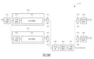
第2圖為根據本發明一實施例之影像處理電路110的示意圖。如第2圖所示,影像處理電路110包含有一分離電路(splitter)210、一第一通道220、一第二通道230、選擇電路241、242、一仲裁器(arbiter)250、一壓縮電路260、一分離電路270、選擇電路281、282、寫入直接記憶體存取(Write Direct Memory Access,WDMA)電路280、290,其中第一通道220包含了一切割(crop)電路222及一縮放電路224;第二通道230包含了一切割電路232及一縮放電路234。FIG. 2 is a schematic diagram of an
在影像處理電路110的操作中,首先,分離電路210接收影像資料Din,並將影像資料分流至第一通道220與第二通道230。在一實施例中,分離電路210係透過單一個端口(port)接收影像資料Din,而第一通道220與第二通道230的每一者都會接收到完整的影像資料Din。接著,關於第一通道220的操作,切割電路222會對影像資料Din中各圖框進行裁切以留下所需要的區域,並將所需要之區域的資料傳送至縮放電路224。縮放電路224用以對所需要之區域的資料進行影像縮放操作以產生一處理後影像資料D1,並傳送至選擇電路241。舉例來說,縮放電路224可包含多組縮放單元,且縮放電路224可先對接收到的資料進行垂直方向的影像放大(scaling up)操作,以產生垂直放大後影像資料至一線緩衝器(line buffer),再對垂直放大後影像資料進行水平方向的影像放大操作,以產生處理後影像資料D1。第二通道230的操作係類似於第一通道,在此不再贅述。實施上,第一通道220對影像資料Din所進行的裁切及/或縮放處理係不同於第二通道230,例如,第一通道220對影像資料Din所進行縮放比例係不同於第二通道230對影像資料Din所進行縮放比例。需注意的是,上述第一通道220與第二通道230的操作內容與操作順序只是作為範例說明,而非是本發明的限制。In the operation of the
接著,選擇電路241可根據控制訊號Vc1以在適當的時間點傳送處理後影像資料D1至仲裁器250,且選擇電路242可以根據控制訊號Vc2以在適當的時間點傳送處理後影像資料D2至仲裁器250。在一實施例中,選擇電路241與選擇電路242整體來說可以使用一多工器來實現。仲裁器250可以是一個2至1仲裁器(2-t0-1arbiter),其用來自選擇電路241、242的輸出中選擇其一輸入至壓縮電路260。壓縮電路260可以是任何形式的壓縮電路,例如採用Arm圖框緩衝壓縮(Arm Frame Buffer Compression,AFBC)壓縮機制的電路,以交替地對處理後影像資料D1、D2進行壓縮,以分別產生壓縮後影像資料Dcom1、Dcom2。接著,分離電路270將壓縮後影像資料Dcom1透過由控制訊號Vc3控制的選擇電路281傳送至WDMA電路280,以供寫入至環形緩衝器120中;類似地,分離電路270將壓縮後影像資料Dcom2透過由控制訊號Vc4控制的選擇電路282傳送至WDMA電路290,以供寫入至環形緩衝器120中。也就是說,經第一通道220處理後所產生的壓縮後影像資料Dcom1與經第二通道230處理後所產生的壓縮後影像資料Dcom2係共用環形緩衝器120。Then, the
上述選擇電路241、242、仲裁器250、壓縮電路260、分離電路270、選擇電路281、282的操作可以視為對處理後影像資料D1、D2進行分時多工處理,亦即交替地利用壓縮電路260對處理後影像資料D1、D2進行處理以分別產生對應的壓縮後影像資料Dcom1、Dcom2,以供儲存至環形緩衝器120。The operations of the
影像處理電路110中,透過對處理後影像資料D1、D2進行壓縮以產生尺寸較小的壓縮後影像資料Dcom1、Dcom2,可以讓環形緩衝器120可以儲存更多筆的影像資料,或是可以讓環形緩衝器120僅需要設計較小的容量便可以符合需求。此外,透過使用分時多工技術來對處理後影像資料D1、D2進行處理,可以只需要一套壓縮電路便可以達到其功能,故可以降低硬體製造成本。In the
第3圖為根據本發明一實施例之視訊編碼器130的示意圖。如第3圖所示,視訊編碼器130包含了一讀取直接記憶體存取(Read Direct Memory Access,RDMA)電路310、一預載入(pre-load)電路320、一記憶體330、一解壓縮電路340以及一編碼電路350。在視訊編碼器130的操作中,RDMA電路310自環形緩衝器120中讀取先前由影像處理電路110所寫入的壓縮後影像資料Dcom1、Dcom2,並透過預載入電路320暫存至記憶體330。解壓縮電路340可以是對應至壓縮電路260的解壓縮電路,例如採用AFBC機制的解壓縮電路,並透過預載入電路320對壓縮後影像資料Dcom1、Dcom2進行解壓縮操作,以產生解壓縮後影像資料。接著,編碼電路對解壓縮後影像資料進行編碼操作,例如符合高效率視訊編碼(High Efficiency Video Coding)之H.264、H.265規格的編碼操作,以產生編碼後影像資料Denc。FIG. 3 is a schematic diagram of a
為了讓環形緩衝器120的尺寸可確實地減少而不影響到影像處理電路110與視訊編碼器130的操作,並實現壓縮後影像資料Dcom1、Dcom2共用環形緩衝器120,需有效率地控制影像處理電路110及視訊編碼器130的資料處理與傳遞,亦即,前一級電路的資料處理完後可以迅速地送往下一級電路進行處理,其具體內容如下所述。In order to reduce the size of the
在一實施例中,視訊處理電路100藉由一些全域暫存器將一記憶體晶片中一記憶區塊配置為環形緩衝器120,全域暫存器的所儲存的內容包含環形緩衝器120的起始位址、環形緩衝器120的大小、環形緩衝器120中項目的數量、目前環形緩衝器120的寫入指標、目前環形緩衝器120的讀取指標等。當WDMA電路280、290分別將壓縮後影像資料Dcom1、Dcom2寫入至環形緩衝器120時,WDMA電路280、290亦會根據全域暫存器的內容來建立一寫入資料表,以記錄寫入至環形緩衝器120中之資料的資訊。以第4圖為例來進行說明,假設WDMA電路280、290在將對應至一圖框的壓縮後影像資料寫入至環形緩衝器120時會在一寫入資料表400建立一個項目(entry)的資訊,則當WDMA電路280、290將對應至一第一圖框的壓縮後影像資料寫入至環形緩衝器120時,WDMA電路280、290在寫入資料表400中的項目0建立第一圖框之壓縮後影像資料在環形緩衝器120中的起始位址、第一圖框之壓縮後影像資料的大小、以及第一圖框之的壓縮後影像資料的相關資訊,其中該相關資訊包含有第一圖框之的壓縮後影像資料的狀態(例如,預設狀態、正在進行寫入或是已經完成寫入)、第一圖框的圖框索引(frame index)、通道索引(對應到第一通道220或是第二通道230)等。其中,圖框索引係用以識別所對應的圖框(例如圖框序號),而通道索引用以識別所對應的通道。由於環形緩衝器120係由第一通道及第二通道共用,藉由在各項目中記錄各圖框的圖框索引、及通道索引,讓視訊編碼器130得以據以識別及讀取環形緩衝器120中所儲存的資料。In one embodiment, the
同樣地,當WDMA電路280、290將對應至一第二圖框、一第三圖框、一第四圖框的壓縮後影像資料寫入至環形緩衝器120時,WDMA電路280、290會分別在寫入資料表400中的項目1、2、3中記錄第二圖框、第三圖框、第四圖框之壓縮後影像資料在環形緩衝器120中的起始位址、壓縮後影像資料的大小、以及的壓縮後影像資料的相關資訊。接著,當WDMA電路280、290將對應至一第五圖框的壓縮後影像資料寫入至環形緩衝器120時,WDMA電路280、290會分別在寫入資料表400中的項目0中記錄第五圖框的資訊,以覆蓋之前所儲存之第一圖框的資訊。Similarly, when the
在一實施例中,寫入資料表400可儲存在對應於WDMA電路280、290的一第一暫存器中,第一暫存器可由多個暫存單元構成,用以儲存寫入資料表中多個項目。而視訊編碼器130內的RDMA電路310可建立一讀取資料表以記錄自環形緩衝器120中所讀取之資料的資訊,讀取資料表可儲存於一第二暫存器中,第二暫存器亦由暫存單元構成。實施上,讀取資料表可僅包括一項目,因此,第二暫存器內的暫存單元係少於第一暫存器內的暫存單元,藉以降低第二暫存器的硬體成本。In one embodiment, the write data table 400 may be stored in a first register corresponding to the
在一實施例中,可透過一機制將第一暫存器內寫入資料表400各項目的資料傳送至第二暫存器內的讀取資料表,以供視訊編碼器130據以讀取環形緩衝器120內的影像資料。在一實施例中,第一暫存器與第二暫存器間係以專屬的硬體線路來進行連接,亦即給視訊編碼器130在取得寫入資料表400的過程可以不需要透過中央處理器或是軟體的控制。以第5圖為例來進行說明,影像處理電路110內可以具有一多工器510,其根據一選擇訊號Vs以依序選擇項目0、項目1、項目2、項目3,之後再重新選擇項目0、項目1、項目2、項目3、...以此類推,以將對應之圖框的起始位址、大小、資訊傳送至視訊編碼器130。此外,在一實施例中,選擇訊號Vs是由視訊編碼器130所產生,並且是具有一特定頻率的時脈訊號,視訊編碼器130可藉由選擇訊號Vs來選擇寫入資料表400內的一項目,且多工器510可以透過選擇訊號Vs之上緣觸發以傳送一個項目的內容至第二暫存器,亦即在每一個時脈訊號的週期,視訊編碼器130都可以自寫入資料表400中取得一個項目的資訊至讀取資料表。In one embodiment, the data of each item written into the data table 400 in the first register can be transmitted to the read data table in the second register through a mechanism, so that the
在接收到某一個項目所帶有之起始位址、大小、資訊後,例如項目0所帶有之第一圖框之壓縮後資料在環形緩衝器120內的起始位址、大小、圖框相關資訊後,視訊編碼器130便可以根據項目0內的內容得知第一圖框之壓縮後資料在環形緩衝器120的位址、所對應的圖框序號及通道等訊息,並以自環形緩衝器120中讀取第一圖框的壓縮後資料,以供後續的操作。在另一實施例中,視訊編碼器130可以在讀取寫入資料表400的多個項目後,根據多個項目的內容來決定後續對環形緩衝器120內之壓縮後資料進行編碼的流程。After receiving the starting address, size, and information of a certain item, for example, the starting address, size, and frame-related information of the compressed data of the first frame in item 0 in the
在第4、5圖的實施例中,透過將寫入資料表400的資料傳送至視訊編碼器130對應的第二暫存器,可以讓視訊編碼器130據以快速地自環形緩衝器120讀取所需的資料。此外,透過使用多工器510,可以在只需要一個硬體線路的情形下依序將不同項目的資料傳送至視訊編碼器130,以降低硬體成本。In the embodiments of Figures 4 and 5, by transmitting the data written into the data table 400 to the second register corresponding to the
在一實施例中,由於影像資料Din包含了亮度(Y)以及色度(UV)資料,因此,環形緩衝器120可以包含一第一環形緩衝器與一第二環形緩衝器,第一環形緩衝器用以儲存壓縮後亮度資料,而第二環形緩衝器用以儲存壓縮後色度資料。此時,在第4、5圖的實施例中,寫入資料表400中每一個項目所帶有之起始位址、大小、資訊可以包含壓縮後亮度資料在第一環形緩衝器中的起始位址、壓縮後亮度資料的大小、以及壓縮後亮度資料的資訊、壓縮後色度資料在第二環形緩衝器中的起始位址、壓縮後色度資料的大小、以及壓縮後色度資料的資訊,其中壓縮後亮度資料的資訊包含壓縮後亮度資料的狀態(例如,預設狀態、正在進行寫入或是已經完成寫入)、以及相關的圖框索引與通道索引,且壓縮後色度資料的資訊包含壓縮後色度資料的狀態(例如,預設狀態、正在進行寫入或是已經完成寫入)、以及相關的圖框索引與通道索引。在另一實施例中,由於影像資料Din可另外包含亮度標頭(header)與色度標頭資料,因此,除了上述的第一環形緩衝器與第二環形緩衝器,環形緩衝器120可以再包含一第三環形緩衝器與一第四環形緩衝器,第三環形緩衝器用以儲存壓縮後亮度標頭資料,而第四環形緩衝器用以儲存壓縮後色度標頭資料。此時,在第4、5圖的實施例中,寫入資料表400中每一個項目所帶有之起始位址、大小、資訊可以另外包含壓縮後亮度標頭資料在第三環形緩衝器中的起始位址、壓縮後亮度資料的大小、以及壓縮後亮度標頭資料的資訊、壓縮後色度標頭資料在第二環形緩衝器中的起始位址、壓縮後色度標頭資料的大小、以及壓縮後色度標頭資料的資訊。如上所述,透過上述寫入資料表400的每一個項目的內容,可以讓視訊編碼器130一次便可以取得亮度以及色度資料的相關資訊,以增進視訊編碼器130的讀取效率。In one embodiment, since the image data Din includes brightness (Y) and chrominance (UV) data, the
需注意的是,在第1圖的實施例中,影像處理電路110係將壓縮後影像資料寫入至環形緩衝器120,以供視訊編碼器130使用但本發明不以此為限。在本發明的其他實施例中,視訊編碼器130可以被替換為其他的後級電路,例如後級影像處理電路。這些設計上的變化應隸屬於本發明的範疇。It should be noted that in the embodiment of FIG. 1, the
簡要歸納本發明,在本發明之視訊處理電路中,透過將多個通道的處理後影像資料進行壓縮並讓多個通道共用同一個環形緩衝器,讓環形緩衝器可以儲存更多筆的影像資料或是讓環形緩衝器僅需要較小的容量便可以符合需求,而透過使用分時多工技術來對處理後影像資料進行壓縮,可以只需要一套壓縮電路便可以達到其功能,故可以降低硬體製造成本。此外,本發明一實施例係另外建立一寫入資料表,其包含了每一個圖框之壓縮後資料在環形緩衝器內的起始位址、大小、狀態、圖框索引及通道索引,且可以將每一個項目透過多工器來傳送至後級電路,以供有效率地自環形緩衝器內讀取所需的資料。To briefly summarize the present invention, in the video processing circuit of the present invention, by compressing the processed image data of multiple channels and allowing the multiple channels to share the same annular buffer, the annular buffer can store more image data or the annular buffer only needs a smaller capacity to meet the demand. By using time-division multiplexing technology to compress the processed image data, only one set of compression circuits is needed to achieve its function, thereby reducing the hardware manufacturing cost. In addition, an embodiment of the present invention is to establish a write data table, which includes the starting address, size, status, frame index and channel index of each frame's compressed data in the ring buffer, and each item can be transmitted to the subsequent circuit through a multiplexer to efficiently read the required data from the ring buffer.
以上所述僅為本發明之較佳實施例,凡依本發明申請專利範圍所做之均等變化與修飾,皆應屬本發明之涵蓋範圍。The above is only the preferred embodiment of the present invention. All equivalent changes and modifications made according to the scope of the patent application of the present invention shall fall within the scope of the present invention.
110:影像處理電路110: Image processing circuit
210:分離電路210: Separation circuit
220:第一通道220: First channel
222:切割電路222: Cutting circuit
224:縮放電路224: Scaling circuit
230:第二通道230: Second channel
232:切割電路232: Cutting circuit
234:縮放電路234: Scaling circuit
241,242:選擇電路241,242: Select circuit
250:仲裁器250:Arbitrator
260:壓縮電路260:Compression circuit
270:分離電路270: Separation circuit
281,282:選擇電路281,282: Select circuit
280,290:WDMA電路280,290:WDMA circuit
D1,D2:處理後影像資料D1, D2: processed image data
Dcom1,Dcom2:壓縮後影像資料Dcom1, Dcom2: compressed image data
Vc1,Vc2,Vc3,Vc4:控制訊號Vc1, Vc2, Vc3, Vc4: control signal
Claims (9)
Translated fromChinesePriority Applications (1)
| Application Number | Priority Date | Filing Date | Title |
|---|---|---|---|
| TW111139183ATWI859602B (en) | 2022-10-17 | 2022-10-17 | Video processing circuit and associated video processing method |
Applications Claiming Priority (1)
| Application Number | Priority Date | Filing Date | Title |
|---|---|---|---|
| TW111139183ATWI859602B (en) | 2022-10-17 | 2022-10-17 | Video processing circuit and associated video processing method |
Publications (2)
| Publication Number | Publication Date |
|---|---|
| TW202418803A TW202418803A (en) | 2024-05-01 |
| TWI859602Btrue TWI859602B (en) | 2024-10-21 |
Family
ID=92074358
Family Applications (1)
| Application Number | Title | Priority Date | Filing Date |
|---|---|---|---|
| TW111139183ATWI859602B (en) | 2022-10-17 | 2022-10-17 | Video processing circuit and associated video processing method |
Country Status (1)
| Country | Link |
|---|---|
| TW (1) | TWI859602B (en) |
Citations (3)
| Publication number | Priority date | Publication date | Assignee | Title |
|---|---|---|---|---|
| TW201233189A (en)* | 2011-01-17 | 2012-08-01 | Mediatek Inc | Buffering apparatus and method for buffering multi-partition video/image bitstream |
| TW202121336A (en)* | 2019-11-15 | 2021-06-01 | 美商英特爾股份有限公司 | Parallel decompression mechanism |
| TW202205198A (en)* | 2020-07-22 | 2022-02-01 | 瑞昱半導體股份有限公司 | Image processing device |
- 2022
- 2022-10-17TWTW111139183Apatent/TWI859602B/enactive
Patent Citations (3)
| Publication number | Priority date | Publication date | Assignee | Title |
|---|---|---|---|---|
| TW201233189A (en)* | 2011-01-17 | 2012-08-01 | Mediatek Inc | Buffering apparatus and method for buffering multi-partition video/image bitstream |
| TW202121336A (en)* | 2019-11-15 | 2021-06-01 | 美商英特爾股份有限公司 | Parallel decompression mechanism |
| TW202205198A (en)* | 2020-07-22 | 2022-02-01 | 瑞昱半導體股份有限公司 | Image processing device |
Also Published As
| Publication number | Publication date |
|---|---|
| TW202418803A (en) | 2024-05-01 |
Similar Documents
| Publication | Publication Date | Title |
|---|---|---|
| CN101188778B (en) | Device and method for outputting video stream | |
| US9179155B1 (en) | Skipped macroblock video encoding enhancements | |
| CN114428595B (en) | Image processing method, device, computer equipment and storage medium | |
| US7936375B2 (en) | Image processor, imaging device, and image processing system use with image memory | |
| CN115801968B (en) | Video processing circuit and related video processing method | |
| US8204318B2 (en) | Method and apparatus for image compression and decompression | |
| US10855917B2 (en) | Data processing method and device, chip, and camera | |
| TWI859602B (en) | Video processing circuit and associated video processing method | |
| CN108668169B (en) | Image information processing method and device, and storage medium | |
| US20060033753A1 (en) | Apparatuses and methods for incorporating an overlay within an image | |
| US8482438B2 (en) | Data processing device and data processing method | |
| CN109274955B (en) | Compression and synchronization method and system for light field video and depth map, and electronic equipment | |
| US7391932B2 (en) | Apparatus and method for selecting image to be displayed | |
| CN108876703B (en) | Data storage method | |
| JP2017055217A (en) | Image processing apparatus and image processing method and imaging device | |
| CN102132568A (en) | motion detection device | |
| US8036476B2 (en) | Image encoding/decoding device and method thereof with data blocks in a determined order | |
| CN118735766B (en) | Image data processing method and device | |
| US20060294324A1 (en) | Modularly configurable memory system for LCD TV system | |
| KR20210134947A (en) | Cooperative access method and system of external memory, cooperative access architecture | |
| TW577229B (en) | Module and method for graphics display | |
| JP2011139175A (en) | Image processing apparatus and image processing method | |
| US20060007237A1 (en) | Apparatuses and methods for sharing a memory between display data and compressed display data | |
| JPH05282191A (en) | Video field memory device for multiple system | |
| JPH0283578A (en) | Image data display device and image data display method |