TWI858304B - Substrate processing apparatus and substrate processing method - Google Patents
Substrate processing apparatus and substrate processing methodDownload PDFInfo
- Publication number
- TWI858304B TWI858304BTW110149552ATW110149552ATWI858304BTW I858304 BTWI858304 BTW I858304BTW 110149552 ATW110149552 ATW 110149552ATW 110149552 ATW110149552 ATW 110149552ATW I858304 BTWI858304 BTW I858304B
- Authority
- TW
- Taiwan
- Prior art keywords
- substrate
- edge electrode
- substrate processing
- insulating ring
- chuck
- Prior art date
Links
Images


Classifications
- H—ELECTRICITY
- H01—ELECTRIC ELEMENTS
- H01J—ELECTRIC DISCHARGE TUBES OR DISCHARGE LAMPS
- H01J37/00—Discharge tubes with provision for introducing objects or material to be exposed to the discharge, e.g. for the purpose of examination or processing thereof
- H01J37/32—Gas-filled discharge tubes
- H01J37/32431—Constructional details of the reactor
- H01J37/32532—Electrodes
- H01J37/32568—Relative arrangement or disposition of electrodes; moving means
- H—ELECTRICITY
- H01—ELECTRIC ELEMENTS
- H01J—ELECTRIC DISCHARGE TUBES OR DISCHARGE LAMPS
- H01J37/00—Discharge tubes with provision for introducing objects or material to be exposed to the discharge, e.g. for the purpose of examination or processing thereof
- H01J37/32—Gas-filled discharge tubes
- H01J37/32009—Arrangements for generation of plasma specially adapted for examination or treatment of objects, e.g. plasma sources
- H01J37/32366—Localised processing
- H01J37/32385—Treating the edge of the workpieces
- H—ELECTRICITY
- H01—ELECTRIC ELEMENTS
- H01J—ELECTRIC DISCHARGE TUBES OR DISCHARGE LAMPS
- H01J37/00—Discharge tubes with provision for introducing objects or material to be exposed to the discharge, e.g. for the purpose of examination or processing thereof
- H01J37/32—Gas-filled discharge tubes
- H01J37/32009—Arrangements for generation of plasma specially adapted for examination or treatment of objects, e.g. plasma sources
- H01J37/32082—Radio frequency generated discharge
- H01J37/32091—Radio frequency generated discharge the radio frequency energy being capacitively coupled to the plasma
- H—ELECTRICITY
- H01—ELECTRIC ELEMENTS
- H01J—ELECTRIC DISCHARGE TUBES OR DISCHARGE LAMPS
- H01J37/00—Discharge tubes with provision for introducing objects or material to be exposed to the discharge, e.g. for the purpose of examination or processing thereof
- H01J37/32—Gas-filled discharge tubes
- H01J37/32431—Constructional details of the reactor
- H01J37/3244—Gas supply means
- H01J37/32449—Gas control, e.g. control of the gas flow
- H—ELECTRICITY
- H01—ELECTRIC ELEMENTS
- H01J—ELECTRIC DISCHARGE TUBES OR DISCHARGE LAMPS
- H01J37/00—Discharge tubes with provision for introducing objects or material to be exposed to the discharge, e.g. for the purpose of examination or processing thereof
- H01J37/32—Gas-filled discharge tubes
- H01J37/32431—Constructional details of the reactor
- H01J37/32532—Electrodes
- H01J37/32541—Shape
- H—ELECTRICITY
- H01—ELECTRIC ELEMENTS
- H01J—ELECTRIC DISCHARGE TUBES OR DISCHARGE LAMPS
- H01J37/00—Discharge tubes with provision for introducing objects or material to be exposed to the discharge, e.g. for the purpose of examination or processing thereof
- H01J37/32—Gas-filled discharge tubes
- H01J37/32431—Constructional details of the reactor
- H01J37/32623—Mechanical discharge control means
- H01J37/32642—Focus rings
- H—ELECTRICITY
- H01—ELECTRIC ELEMENTS
- H01J—ELECTRIC DISCHARGE TUBES OR DISCHARGE LAMPS
- H01J37/00—Discharge tubes with provision for introducing objects or material to be exposed to the discharge, e.g. for the purpose of examination or processing thereof
- H01J37/32—Gas-filled discharge tubes
- H01J37/32431—Constructional details of the reactor
- H01J37/32715—Workpiece holder
- H—ELECTRICITY
- H01—ELECTRIC ELEMENTS
- H01L—SEMICONDUCTOR DEVICES NOT COVERED BY CLASS H10
- H01L21/00—Processes or apparatus adapted for the manufacture or treatment of semiconductor or solid state devices or of parts thereof
- H01L21/67—Apparatus specially adapted for handling semiconductor or electric solid state devices during manufacture or treatment thereof; Apparatus specially adapted for handling wafers during manufacture or treatment of semiconductor or electric solid state devices or components ; Apparatus not specifically provided for elsewhere
- H01L21/67005—Apparatus not specifically provided for elsewhere
- H01L21/67011—Apparatus for manufacture or treatment
- H01L21/67017—Apparatus for fluid treatment
- H01L21/67063—Apparatus for fluid treatment for etching
- H01L21/67069—Apparatus for fluid treatment for etching for drying etching
- H—ELECTRICITY
- H01—ELECTRIC ELEMENTS
- H01J—ELECTRIC DISCHARGE TUBES OR DISCHARGE LAMPS
- H01J2237/00—Discharge tubes exposing object to beam, e.g. for analysis treatment, etching, imaging
- H01J2237/32—Processing objects by plasma generation
- H01J2237/33—Processing objects by plasma generation characterised by the type of processing
- H01J2237/334—Etching
- H—ELECTRICITY
- H01—ELECTRIC ELEMENTS
- H01L—SEMICONDUCTOR DEVICES NOT COVERED BY CLASS H10
- H01L21/00—Processes or apparatus adapted for the manufacture or treatment of semiconductor or solid state devices or of parts thereof
- H01L21/67—Apparatus specially adapted for handling semiconductor or electric solid state devices during manufacture or treatment thereof; Apparatus specially adapted for handling wafers during manufacture or treatment of semiconductor or electric solid state devices or components ; Apparatus not specifically provided for elsewhere
- H01L21/683—Apparatus specially adapted for handling semiconductor or electric solid state devices during manufacture or treatment thereof; Apparatus specially adapted for handling wafers during manufacture or treatment of semiconductor or electric solid state devices or components ; Apparatus not specifically provided for elsewhere for supporting or gripping
- H01L21/687—Apparatus specially adapted for handling semiconductor or electric solid state devices during manufacture or treatment thereof; Apparatus specially adapted for handling wafers during manufacture or treatment of semiconductor or electric solid state devices or components ; Apparatus not specifically provided for elsewhere for supporting or gripping using mechanical means, e.g. chucks, clamps or pinches
- H01L21/68714—Apparatus specially adapted for handling semiconductor or electric solid state devices during manufacture or treatment thereof; Apparatus specially adapted for handling wafers during manufacture or treatment of semiconductor or electric solid state devices or components ; Apparatus not specifically provided for elsewhere for supporting or gripping using mechanical means, e.g. chucks, clamps or pinches the wafers being placed on a susceptor, stage or support
- H01L21/68735—Apparatus specially adapted for handling semiconductor or electric solid state devices during manufacture or treatment thereof; Apparatus specially adapted for handling wafers during manufacture or treatment of semiconductor or electric solid state devices or components ; Apparatus not specifically provided for elsewhere for supporting or gripping using mechanical means, e.g. chucks, clamps or pinches the wafers being placed on a susceptor, stage or support characterised by edge profile or support profile
- H—ELECTRICITY
- H01—ELECTRIC ELEMENTS
- H01L—SEMICONDUCTOR DEVICES NOT COVERED BY CLASS H10
- H01L21/00—Processes or apparatus adapted for the manufacture or treatment of semiconductor or solid state devices or of parts thereof
- H01L21/67—Apparatus specially adapted for handling semiconductor or electric solid state devices during manufacture or treatment thereof; Apparatus specially adapted for handling wafers during manufacture or treatment of semiconductor or electric solid state devices or components ; Apparatus not specifically provided for elsewhere
- H01L21/683—Apparatus specially adapted for handling semiconductor or electric solid state devices during manufacture or treatment thereof; Apparatus specially adapted for handling wafers during manufacture or treatment of semiconductor or electric solid state devices or components ; Apparatus not specifically provided for elsewhere for supporting or gripping
- H01L21/687—Apparatus specially adapted for handling semiconductor or electric solid state devices during manufacture or treatment thereof; Apparatus specially adapted for handling wafers during manufacture or treatment of semiconductor or electric solid state devices or components ; Apparatus not specifically provided for elsewhere for supporting or gripping using mechanical means, e.g. chucks, clamps or pinches
- H01L21/68714—Apparatus specially adapted for handling semiconductor or electric solid state devices during manufacture or treatment thereof; Apparatus specially adapted for handling wafers during manufacture or treatment of semiconductor or electric solid state devices or components ; Apparatus not specifically provided for elsewhere for supporting or gripping using mechanical means, e.g. chucks, clamps or pinches the wafers being placed on a susceptor, stage or support
- H01L21/68742—Apparatus specially adapted for handling semiconductor or electric solid state devices during manufacture or treatment thereof; Apparatus specially adapted for handling wafers during manufacture or treatment of semiconductor or electric solid state devices or components ; Apparatus not specifically provided for elsewhere for supporting or gripping using mechanical means, e.g. chucks, clamps or pinches the wafers being placed on a susceptor, stage or support characterised by a lifting arrangement, e.g. lift pins
Landscapes
- Engineering & Computer Science (AREA)
- Physics & Mathematics (AREA)
- Plasma & Fusion (AREA)
- Chemical & Material Sciences (AREA)
- Analytical Chemistry (AREA)
- General Physics & Mathematics (AREA)
- Condensed Matter Physics & Semiconductors (AREA)
- Manufacturing & Machinery (AREA)
- Computer Hardware Design (AREA)
- Microelectronics & Electronic Packaging (AREA)
- Power Engineering (AREA)
- Drying Of Semiconductors (AREA)
- Chemical Vapour Deposition (AREA)
Abstract
Translated fromChineseDescription
Translated fromChinese本發明係關於基板處理設備及基板處理方法。The present invention relates to a substrate processing device and a substrate processing method.
電漿係指由離子或自由基以及電子等構成的離子化的氣體狀態,藉助於極高的溫度或強電場或高頻電磁場(RF Electromagnetic Fields)而產生。半導體元件製造製程包括利用電漿去除基板上的膜質的灰化或蝕刻製程。灰化或蝕刻製程藉由電漿含有的離子及自由基粒子與基板上的膜質碰撞或反應而執行。利用電漿處理基板的製程以多種方式執行。在利用電漿處理基板的方法中,斜面蝕刻製程在基板的邊緣區域產生電漿,去除基板的邊緣區域上的薄膜。Plasma refers to an ionized gas state composed of ions or free radicals and electrons, etc., which is generated by extremely high temperature or strong electric field or high frequency electromagnetic field (RF Electromagnetic Fields). The semiconductor device manufacturing process includes an ashing or etching process that uses plasma to remove the film on the substrate. The ashing or etching process is performed by the collision or reaction of the ions and free radical particles contained in the plasma with the film on the substrate. The process of using plasma to treat the substrate is performed in a variety of ways. In the method of using plasma to treat the substrate, the bevel etching process generates plasma at the edge area of the substrate to remove the thin film on the edge area of the substrate.
另一方面,在執行這種斜面蝕刻製程方面,要求根據處理條件來調節電漿產生的區域(所謂製程區域)的尺寸和位置。一般係更換斜面蝕刻設備具有的構成,以調節這種製程區域的尺寸和位置。但是,這種方法在更換構成所需的時間內無法處理基板,降低了基板處理效率。另外,在根據處理配方處理基板過程中,會需要變更製程區域的尺寸和位置,在原有方式的情況下,無法變更製程區域的尺寸和位置,或即使可變更,變更範圍也極為有限。On the other hand, in executing this bevel etching process, it is required to adjust the size and position of the area where the plasma is generated (the so-called process area) according to the processing conditions. Generally, the structure of the bevel etching equipment is replaced to adjust the size and position of this process area. However, this method cannot process the substrate within the time required to replace the structure, which reduces the substrate processing efficiency. In addition, in the process of processing the substrate according to the processing recipe, it is necessary to change the size and position of the process area. Under the original method, the size and position of the process area cannot be changed, or even if it can be changed, the range of change is extremely limited.
[技術課題][Technical topics]
本發明一個目的係提供一種能夠高效處理基板的基板處理設備及基板處理方法。An object of the present invention is to provide a substrate processing apparatus and a substrate processing method capable of efficiently processing a substrate.
另外,本發明一個目的係提供一種能夠變更在基板的邊緣區域產生的電漿的位置的基板處理設備及基板處理方法。In addition, an object of the present invention is to provide a substrate processing apparatus and a substrate processing method capable of changing the position of plasma generated in the edge area of the substrate.
另外,本發明一個目的係提供一種能夠變更電漿產生的區域的尺寸的基板處理設備及基板處理方法。In addition, an object of the present invention is to provide a substrate processing apparatus and a substrate processing method capable of changing the size of a plasma generating area.
另外,本發明一個目的係提供一種提供可控制電漿流動的追加控制因子的基板處理設備及基板處理方法。In addition, an object of the present invention is to provide a substrate processing apparatus and a substrate processing method that provide an additional control factor for controlling plasma flow.
本發明要解決的課題並非限定於上述課題,本發明所屬技術領域的技藝人士可從本說明書及圖式明確理解未提及的課題。 [技術方案]The issues to be solved by the present invention are not limited to the above-mentioned issues. A person skilled in the art in the technical field to which the present invention belongs can clearly understand the issues not mentioned from this specification and drawings.[Technical Solution]
本發明提供處理基板的設備。處理基板的設備可包括:殼體,前述殼體具有內部空間;支撐單元,前述支撐單元在前述內部空間中支撐基板;氣體供應單元,前述氣體供應單元向前述內部空間供應氣體;電源構件,前述電源構件激發前述氣體而產生電漿;以及上部邊緣電極,前述上部邊緣電極在被前述支撐單元支撐的基板的邊緣區域產生前述電漿;其中,前述支撐單元可包括:卡盤,前述卡盤支撐基板;下部邊緣電極,前述下部邊緣電極與前述上部邊緣電極面對面;絕緣環,前述絕緣環配置於前述下部邊緣電極與前述卡盤之間;以及移動構件,前述移動構件使前述下部邊緣電極或前述絕緣環沿上下方向移動。The present invention provides a device for processing a substrate. The device for processing a substrate may include: a housing, the housing having an internal space; a support unit, the support unit supporting the substrate in the internal space; a gas supply unit, the gas supply unit supplying gas to the internal space; a power supply component, the power supply component exciting the gas to generate plasma; and an upper edge electrode, the upper edge electrode being disposed on the substrate supported by the support unit. The plasma is generated in the edge area of the substrate; wherein the supporting unit may include: a chuck, the chuck supports the substrate; a lower edge electrode, the lower edge electrode faces the upper edge electrode; an insulating ring, the insulating ring is arranged between the lower edge electrode and the chuck; and a moving component, the moving component moves the lower edge electrode or the insulating ring in the up and down direction.
根據一實施例,可進一步包括:移動電源,前述移動電源傳遞驅動前述移動構件的電力。According to one embodiment, it may further include: a mobile power source, the mobile power source transmits power to drive the mobile component.
根據一實施例,前述移動構件可為壓電馬達。According to one embodiment, the aforementioned moving component may be a piezoelectric motor.
根據一實施例,藉助於前述移動構件而向上移動的前述絕緣環或前述下部邊緣電極的上端高度可小於或等於前述卡盤的上端高度。According to one embodiment, the upper end height of the aforementioned insulating ring or the aforementioned lower edge electrode moved upward by means of the aforementioned moving member may be less than or equal to the upper end height of the aforementioned chuck.
根據一實施例,前述移動構件可以使前述下部邊緣電極和前述絕緣環中的前述絕緣環移動的方式構成。According to one embodiment, the moving member can be configured to move the lower edge electrode and the insulating ring.
根據一實施例,前述移動構件可配置於比前述絕緣環更下部。According to one embodiment, the moving member may be disposed below the insulating ring.
根據一實施例,從主剖面觀察的前述絕緣環的寬度可小於從上部觀察的前述卡盤外周與前述下部邊緣電極內周之間的距離。According to one embodiment, the width of the aforementioned insulating ring observed from the main cross-section may be smaller than the distance between the aforementioned outer periphery of the chuck and the aforementioned inner periphery of the lower edge electrode observed from the top.
根據一實施例,前述絕緣環可配置為與前述下部邊緣電極及/或前述卡盤隔開。According to one embodiment, the insulating ring may be configured to be separated from the lower edge electrode and/or the chuck.
根據一實施例,前述絕緣環與前述下部邊緣電極之間的間隔可為0.2mm至0.5mm。According to one embodiment, the spacing between the insulating ring and the lower edge electrode may be 0.2 mm to 0.5 mm.
根據一實施例,前述絕緣環與前述卡盤之間的間隔可為0.2mm至0.5mm。According to one embodiment, the spacing between the insulating ring and the chuck may be 0.2 mm to 0.5 mm.
根據一實施例,前述設備可進一步包括控制前述支撐單元的控制器,前述控制器在增大前述電漿的每單位面積的密度時,可使前述下部邊緣電極以及前述絕緣環中至少一個向上移動,在減小前述電漿的每單位面積的密度時,可使前述下部邊緣電極以及前述絕緣環中至少一個向下移動。According to one embodiment, the aforementioned device may further include a controller for controlling the aforementioned support unit, and the aforementioned controller may cause at least one of the aforementioned lower edge electrode and the aforementioned insulating ring to move upward when increasing the density per unit area of the aforementioned plasma, and may cause at least one of the aforementioned lower edge electrode and the aforementioned insulating ring to move downward when reducing the density per unit area of the aforementioned plasma.
根據一實施例,前述設備可進一步包括控制前述支撐單元的控制器,前述控制器在利用前述電漿處理被前述支撐單元支撐的基板期間,可使前述下部邊緣電極以及前述絕緣環中至少一個沿上下方向移動。According to one embodiment, the aforementioned apparatus may further include a controller for controlling the aforementioned support unit, and the aforementioned controller may move at least one of the aforementioned lower edge electrode and the aforementioned insulating ring in an up-down direction during the period of using the aforementioned plasma to process the substrate supported by the aforementioned support unit.
另外,本發明提供一種基板處理方法,前述基板處理方法利用斜面蝕刻設備處理前述基板的邊緣區域,其中,前述斜面蝕刻設備包括:卡盤,前述卡盤支撐基板;上部邊緣電極,前述上部邊緣電極在前述基板的邊緣區域產生電漿;下部邊緣電極,前述下部邊緣電極與前述上部邊緣電極面對面;絕緣環,前述絕緣環配置於前述卡盤與前述下部邊緣電極之間。基板處理方法可包括:向前述基板的邊緣區域供應製程氣體並激發前述製程氣體以產生前述電漿,為了調節前述電漿的每單位面積的密度而調節前述絕緣環與前述上部邊緣電極之間的間隔以及前述下部邊緣電極與前述上部邊緣電極之間的間隔中至少一個的間隔。In addition, the present invention provides a substrate processing method, wherein the substrate processing method uses a bevel etching device to process the edge area of the substrate, wherein the bevel etching device includes: a chuck, the chuck supports the substrate; an upper edge electrode, the upper edge electrode generates plasma in the edge area of the substrate; a lower edge electrode, the lower edge electrode faces the upper edge electrode; and an insulating ring, the insulating ring is arranged between the chuck and the lower edge electrode. The substrate processing method may include: supplying a process gas to an edge region of the substrate and exciting the process gas to generate the plasma, and adjusting at least one of the interval between the insulating ring and the upper edge electrode and the interval between the lower edge electrode and the upper edge electrode in order to adjust the density per unit area of the plasma.
根據一實施例,前述間隔的調節可在利用前述電漿處理前述基板期間進行。According to one embodiment, the adjustment of the interval may be performed during the plasma treatment of the substrate.
根據一實施例,前述間隔的調節可在利用前述電漿處理前述基板之前進行。According to one embodiment, the adjustment of the interval may be performed before the substrate is treated with the plasma.
根據實施例,在向前述基板的邊緣區域供應前述製程氣體期間,可為了抑制前述製程氣體進入前述基板的中央區域而向前述基板以及與前述基板面對面配置的介電板之間的空間供應非活性氣體。According to an embodiment, during supplying the process gas to the edge region of the substrate, in order to suppress the process gas from entering the central region of the substrate, an inactive gas may be supplied to the space between the substrate and a dielectric plate disposed opposite to the substrate.
根據一實施例,前述非活性氣體可向前述基板的中央區域供應。According to one embodiment, the inert gas may be supplied to a central area of the substrate.
根據一實施例,可使前述絕緣環以及前述下部邊緣電極中的前述絕緣環沿上下方向移動以調節前述間隔。According to one embodiment, the insulating ring and the insulating ring in the lower edge electrode can be moved in the up-down direction to adjust the interval.
根據一實施例,前述絕緣環可藉助在前述絕緣環下側配置的移動構件而沿上下方向移動。According to one embodiment, the insulating ring can be moved in the up and down direction by means of a moving member arranged at the lower side of the insulating ring.
根據一實施例,可向作為壓電馬達的前述移動構件施加電力以使前述移動構件的尺寸發生變化,尺寸發生變化的前述移動構件可使前述絕緣環向上移動。 [發明效果]According to one embodiment, electric force can be applied to the aforementioned moving member as a piezoelectric motor to change the size of the aforementioned moving member, and the aforementioned moving member with changed size can move the aforementioned insulating ring upward.[Effect of the invention]
根據本發明一實施例,可高效處理基板。According to one embodiment of the present invention, substrates can be processed efficiently.
另外,根據本發明一實施例,可變更在基板的邊緣區域產生的電漿的位置。In addition, according to an embodiment of the present invention, the position of the plasma generated in the edge area of the substrate can be changed.
另外,根據本發明一實施例,可變更電漿產生的區域的尺寸。In addition, according to an embodiment of the present invention, the size of the area where plasma is generated can be changed.
另外,根據本發明一實施例,可提供能夠抑制電漿流動的追加控制因子。In addition, according to an embodiment of the present invention, an additional control factor capable of suppressing plasma flow can be provided.
本發明的效果不限於上述效果,本發明所屬技術領域的技藝人士可從本說明書及圖式明確理解未提及的效果。The effects of the present invention are not limited to the above effects, and those skilled in the art in the technical field to which the present invention belongs can clearly understand the effects not mentioned from this specification and drawings.
下文參考圖式,對本發明的實施例進行詳細說明,以便本發明所屬技術領域的一般技藝人士能夠容易地實施。但是,本發明可以多種不同形態體現,不限定於在此說明的實施例。另外,在詳細說明本發明的較佳實施例方面,在判斷認為對相關公知功能或構成的具體說明可能不必要地混淆本發明的要旨時,省略其詳細說明。另外,對於發揮類似功能和作用的部分,在全體圖式中使用相同的標記。The following is a detailed description of the embodiments of the present invention with reference to the drawings so that a person skilled in the art can easily implement the present invention. However, the present invention can be embodied in a variety of different forms and is not limited to the embodiments described herein. In addition, in the detailed description of the preferred embodiments of the present invention, when it is judged that the specific description of the relevant known functions or components may unnecessarily confuse the gist of the present invention, the detailed description thereof is omitted. In addition, for parts that play similar functions and effects, the same marks are used in the entire drawings.
另外,當提到「包括」某構成元件時,只要沒有特別反對的記載,並非排除其他構成元件,意指可進一步包括其他構成元件。具體地,「包括」或「具有」等術語應理解為係要指定存在說明書上記載的特徵、數字、步驟、動作、構成元件、部件或他們的組合,不預先排除存在或添加一個或其以上的其他特徵或數字、步驟、動作、構成元件、部件或他們的組合的可能性。In addition, when it is mentioned that a certain component is "included", other components are not excluded unless otherwise stated, and it means that other components may be further included. Specifically, the terms "include" or "have" should be understood to specify the existence of features, numbers, steps, actions, components, parts or combinations thereof described in the specification, and do not pre-emptively exclude the possibility of the existence or addition of one or more other features or numbers, steps, actions, components, parts or combinations thereof.
只要上下文未明確表示不同,單數的表達包括複數的表達。另外,為了更明確說明,圖式中的元件的形狀及尺寸等會誇張。Unless the context clearly indicates otherwise, singular expressions include plural expressions. In addition, for the purpose of more clear explanation, the shapes and sizes of the elements in the drawings may be exaggerated.
下文參照圖1至圖8,詳細說明本發明的實施例。The following describes an embodiment of the present invention in detail with reference to FIGS. 1 to 8 .
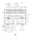
圖1係簡要示出本發明一實施例的基板處理設備的圖。參照圖1,基板處理設備1具有設備前端模組(equipment front end module;EFEM)20和處理模組30。設備前端模組20和處理模組30沿一個方向配置。Fig. 1 is a diagram schematically showing a substrate processing apparatus according to an embodiment of the present invention. Referring to Fig. 1 , the
設備前端模組20具有載入埠(load port)10和移送框架21。載入埠10沿第一方向11配置於設備前端模組20的前方。載入埠10具有多個支撐部6。各個支撐部6沿第二方向12配置成一列,安放有收納將向製程提供的基板W和製程處理完畢的基板W的承載架4(例如載片盒、FOUP(前開式晶圓傳送盒)等)。在承載架4中收納將向製程提供的基板W和製程處理完畢的基板W。移送框架21配置於載入埠10與處理模組30之間。移送框架21包括配置於其內部並在載入埠10與處理模組30間移送基板W的第一移送機器人25。第一移送機器人25沿著沿第二方向12配備的移送軌道27移動,在承載架4與處理模組30間移送基板W。The equipment front-
處理模組30包括裝載閘腔室40、傳輸腔室50及製程腔室60。處理模組30可從設備前端模組20接到移送的基板W並處理基板W。The
裝載閘腔室40鄰接移送框架21配置。作為一個示例,裝載閘腔室40可配置於傳輸腔室50與設備前端模組20之間。裝載閘腔室40提供將向製程提供的基板W在移送到製程腔室60之前或製程處理完畢的基板W在移送到設備前端模組20之前等待的空間。The
傳輸腔室50可傳送基板W。傳輸腔室50鄰接裝載閘腔室40配置。傳輸腔室50從上部觀察時具有多邊形的主體。參照圖1,傳輸腔室50從上部觀察時具有五角形的主體。在主體的外側,沿著主體外周配置有裝載閘腔室40和多個製程腔室60。在主體的各側壁上形成有供基板W進出的通路(未示出),通路連接傳輸腔室50與裝載閘腔室40或製程腔室60。在各通路上提供對通路進行開閉而使內部密閉的門(未示出)。在傳輸腔室50的內部空間,配置有在裝載閘腔室40與製程腔室60間移送基板W的第二移送機器人53。第二移送機器人53將在裝載閘腔室40等待的未處理的基板W移送到製程腔室60,或將製程處理完畢的基板W移送到裝載閘腔室40。另外,第二移送機器人53可向後述的殼體100的內部空間102載入基板W,或從內部空間102載出基板W。另外,第二移送機器人53為了向多個製程腔室60依次提供基板W,可在製程腔室60間移送基板W。如圖1所示,當傳輸腔室50具有五角形的主體時,在與設備前端模組20鄰接的側壁分別配置有裝載閘腔室40,在其餘側壁連續配置有製程腔室60。傳輸腔室50不僅根據前述形狀,而且可根據要求的製程模組而以多樣形態提供。The
製程腔室60可與傳輸腔室50鄰接配置。製程腔室60沿著傳輸腔室50的外周配置。製程腔室60可提供多個。在各個製程腔室60內可執行對基板W的製程處理。製程腔室60從第二移送機器人53接到移送的基板W並執行製程處理,將製程處理完畢的基板W提供給第二移送機器人53。在各個製程腔室60中進行的製程處理可彼此不同。The
下文對製程腔室60中執行電漿製程的基板處理設備1000進行詳細描述。另外,下文說明的基板處理設備1000以構成得能夠對製程腔室60中的基板的邊緣區域執行電漿處理製程的情形為例進行說明。但不限於此,以下說明的基板處理設備1000亦可相同或類似地應用於實現對基板處理的多樣腔室。另外,基板處理設備1000可相同或類似地應用於執行對基板的電漿處理製程的多樣腔室。The following is a detailed description of the
圖2係示出圖1的製程腔室中提供的基板處理設備的一實施例的圖。參照圖2,在製程腔室60中提供的基板處理設備1000利用電漿在基板W上執行既定的製程。作為一個示例,基板處理設備1000可拋光或蝕刻基板W上的膜。膜可為多晶矽膜、矽氧化膜及氮化矽膜等多樣種類的膜。另外,膜可為自然氧化膜或經化學反應而產生的氧化膜。另外,膜可為在處理基板W的過程中產生的副產物(By-Product)。另外,膜可為基板W上附著及/或殘留的雜質。FIG. 2 is a diagram showing an embodiment of a substrate processing device provided in the process chamber of FIG. 1 . Referring to FIG. 2 , the
基板處理設備1000可執行對基板W的電漿製程。例如,基板處理設備1000可供應製程氣體,並使得從供應的製程氣體產生電漿來處理基板W。基板處理設備1000可供應製程氣體,並使得從供應的製程氣體產生電漿來處理基板W的邊緣區域。接著,基板處理設備1000以對基板W的邊緣區域執行蝕刻處理的斜面蝕刻裝置為例進行說明。The
基板處理設備1000可包括殼體100、支撐單元300、介電板單元500、上部電極單元600、溫度調節單元700、氣體供應單元800及控制器900。The
殼體100可定義內部空間102。殼體100可包括上部殼體110(第一殼體的一例)和下部殼體120(第二殼體的一例)。上部殼體110和下部殼體120可相互組合而定義內部空間102。另外,上部殼體110可相對於下部殼體120以能藉助於旋轉結合部(未示出)而旋轉的方式連結。例如,上部殼體110和下部殼體120可藉助於旋轉結合部而連結,前述旋轉結合部可為鉸鏈(Hinge)機構。The
上部殼體110可處於開放位置或處於關閉位置。接著,將上部殼體110與下部殼體120相互組合而定義內部空間102的上部殼體110的位置定義為關閉位置,將使內部空間102暴露於外部的上部殼體110的位置定義為開放位置。The
另外,內部空間102的氣氛在上部殼體110處於關閉位置時與外部隔離,與外部隔離的內部空間102可在基板W處理期間調整為近於真空的低壓狀態(真空壓力氣氛)。另外,殼體100可為包括金屬的材質。另外,殼體100的內表面可用絕緣性材質塗覆。另外,殼體100可接地。In addition, the atmosphere of the
另外,殼體100可為真空腔室。例如,在殼體100的底面可形成有排氣孔104。在內部空間102中產生的電漿P或向內部空間102供應的氣體(G1、G2)可藉由排氣孔104排出到外部。另外,在利用電漿P處理基板W的過程中產生的副產物可藉由排氣孔104排出到外部。另外,排氣孔104可與排氣管線(未示出)連接。排氣管線可與提供減壓的減壓構件連接。減壓構件可藉由排氣管線而向內部空間102提供減壓。In addition, the
支撐單元300可在內部空間102支撐基板W。支撐單元300可包括卡盤310、電源構件320、絕緣環模組330、下部邊緣電極350及驅動構件370。The supporting
卡盤310可在內部空間102支撐基板W。卡盤310可具有支撐基板W的支撐面。卡盤310從上部觀察時可具有圓形。卡盤310從上部觀察時可具有小於基板W的直徑。因此,被卡盤310支撐的基板W的中央區域可安放於卡盤310的支撐面,基板W的邊緣區域可不與卡盤310的支撐面接觸。The
在卡盤310內部可提供加熱裝置(未示出)。加熱裝置(未示出)可加熱卡盤310。加熱裝置可為加熱器。另外,在卡盤310上可形成有冷卻流路312。冷卻流路312可在卡盤310的內部形成。在冷卻流路312上可連接有冷卻流體供應管線314和冷卻流體排出管線316。冷卻流體供應管線314可與冷卻流體供應源318連接。冷卻流體供應源318可儲存冷卻流體及/或向冷卻流體供應管線314供應冷卻流體。另外,向冷卻流路312供應的冷卻流體可藉由冷卻流體排出管線316排出到外部。冷卻流體供應源318儲存及/或供應的冷卻流體可為冷卻液或冷卻氣體。另外,在卡盤310上形成的冷卻流路312的形狀不限於圖2所示的形狀,可多樣地變形。另外,使卡盤310冷卻的構成不限於供應冷卻流體的構成,亦可以能夠使卡盤310冷卻的多樣構成(例如冷卻板等)提供。A heating device (not shown) may be provided inside the
電源構件320可向卡盤310施加電力並激發後述氣體供應單元800供應的氣體以產生電漿。電源構件320可向卡盤310施加RF電力。電源構件320可包括電源322、適配器324及電源線326。電源322可為偏置電源。另外,電源322可為RF電源。電源322可以電源線326為媒介而與卡盤310連接。另外,適配器324可在電源線326上提供,執行阻抗匹配。The
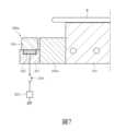
絕緣環模組330可變更製程區域的體積。製程區域可為由絕緣環333、下部邊緣電極350、上部邊緣電極620以及介電板520定義並供處理基板W的邊緣區域的電漿P產生及滯留的區域。絕緣環模組330可包括環主體331、移動構件332、絕緣環333、移動開關334以及移動電源335。The insulating
圖3係示出圖2的卡盤、下部邊緣電極以及絕緣環模組的一部分的剖面圖,圖4係示出圖3的絕緣環向上移動的狀態的圖。FIG3 is a cross-sectional view showing a portion of the chuck, the lower edge electrode, and the insulating ring module of FIG2 , and FIG4 is a view showing a state where the insulating ring of FIG3 is moved upward.
參照圖3及圖4,環主體331可具有環狀。環主體331從上部觀察時可配置於卡盤310以及下部邊緣電極350之間。環主體331從上部觀察時可與卡盤310和下部邊緣電極350結合。環主體331可以具有絕緣性的材料形成。在環主體331的上部可形成有從上向下凹入形成的安放槽。安放槽可形成有多個。安放槽從上部觀察時可沿著環主體331的圓周方向彼此隔開形成。安放槽中可放入後述的移動構件332。3 and 4 , the
移動構件332可使絕緣環333沿上下方向移動。移動構件332可使絕緣環333沿上下方向移動以調節絕緣環333與上部邊緣電極620之間的間隔。所謂絕緣環333與上部邊緣電極620之間的間隔,可意指平行於絕緣環333上面的虛擬直線與平行於上部邊緣電極620下面的虛擬直線之間的間隔。The moving
移動構件332可為壓電馬達(PZT Motor)。移動構件332可根據移動開關334的開啟/關閉而從移動電源335接受電力傳遞。移動電源335可為直流電源。若從移動電源335接受電力傳遞,則移動構件332的尺寸可發生變化。例如,若從移動電源335接受電力傳遞,則移動構件332的尺寸可增大。另外,移動構件332可配置於比絕緣環333更下方。根據移動構件332的尺寸變化,絕緣環333可沿上下方向移動。另外,移動開關334可從後述控制器900接受控制訊號傳遞而開啟/關閉。The moving
在移動構件332的上部可提供絕緣環333。絕緣環333可為具有絕緣性的材料。絕緣環333從上部觀察時可具有環狀。另外,從主剖面觀察的絕緣環333的左右寬度可小於下部邊緣電極350的內周與卡盤310的外周之間的距離。An insulating
絕緣環333可與下部邊緣電極350及/或卡盤310隔開。例如,絕緣環333可與下部邊緣電極350隔開第一間隔D1。另外,絕緣環333可與卡盤310隔開第二間隔D2。第一間隔D1與第二間隔D2可為製程區域產生的電漿P難以穿透的間隔。例如,第一間隔D1可為0.2mm至0.5mm。另外,第二間隔D2亦可為0.2mm至0.5mm。The insulating
再次參照圖2,下部邊緣電極350從上部觀察時可包圍絕緣環333。下部邊緣電極350從上部觀察時可具有環狀。下部邊緣電極350可接地。下部邊緣電極350從上部觀察時可配置於被卡盤310支撐的基板W的邊緣區域下部。基板W的邊緣區域下部從上部觀察時,既可為與基板W的邊緣區域重疊的區域,也可為不重疊的區域。Referring again to FIG. 2 , the
驅動構件370可使卡盤310升降。驅動構件370可包括驅動器372和軸374。軸374可與卡盤310結合。軸374可與驅動器372連接。驅動器372可以軸374為媒介而使卡盤310沿上下方向升降。隨著驅動構件370使卡盤310升降,可調節被卡盤310支撐的基板W的上面與介電板520的下面之間的間隔。The driving
介電板單元500可包括介電板520和第一底座510。另外,介電板單元500可結合於後述的溫度調節板710。The
介電板520的下面可與卡盤310的上面面對面地配置。介電板520從上部觀察時可具有圓形。另外,介電板520的上面可形成錯層,以使其中央區域的高度高於邊緣區域的高度。另外,介電板520的下面可為扁平形狀。另外,在介電板520的下面中,邊緣區域可形成錯層,以使其高度高於中央區域。在介電板520的下面中的錯層區域,使後述的電漿P可進入,可提高對基板W的邊緣區域的處理效率。The bottom of the
介電板520在內部空間102中,可與支撐單元300,具體地,與被卡盤310支撐的基板W上面面對面地配置。介電板520可配置於支撐單元300的上部。介電板520可為包括陶瓷的材質。在介電板520上可形成有與後述的氣體供應單元800的第一氣體供應部810連接的氣體流路。另外,氣體流路的吐出端可構成得使第一氣體供應部810供應的第一氣體G1供應到被支撐單元300支撐的基板W的中央區域。另外,氣體流路的吐出端可構成得使第一氣體G1供應到被支撐單元300支撐的基板W的中央區域上面。The
第一底座510可配置於介電板520與後述的溫度調節板710之間。第一底座510可結合於後述的溫度調節板710,介電板520可結合於第一底座510。因此,介電板520可以第一底座510為媒介而結合於溫度調節板710。The
第一底座510的直徑可從上向下逐漸增大。第一底座510的上面的直徑可小於介電板520的下面。第一底座510的上面可具有扁平形狀。另外,第一底座510的下面可具有錯層形狀。例如,第一底座510的邊緣區域的下面可形成錯層,以使其高度低於中央區域的下面。另外,第一底座510的下面和介電板520的上面可具有能相互組合的形狀。例如,介電板520的中央區域可插入於第一底座510的中央區域。另外,第一底座510可為包括金屬的材質。例如,第一底座510可為包括鋁的材質。介電板520的位置可被第一底座510固定。The diameter of the
上部電極單元600可包括第二底座610和上部邊緣電極620。另外,上部電極單元600可結合於後述的溫度調節板710。上部邊緣電極620可接地。上部邊緣電極620從上部觀察時可具有包圍介電板520的形狀。上部邊緣電極620可與介電板520隔開。上部邊緣電極620可與介電板520隔開而形成隔開空間。隔開空間可形成供後述的第二氣體供應部830供應的第二氣體G2流動的氣體通道中的一部分。氣體通道的吐出端可構成得使第二氣體G2能夠向被支撐單元300支撐的基板W的邊緣區域供應。另外,氣體通道的吐出端可構成得使第二氣體G2向被支撐單元300支撐的基板W的邊緣區域上面供應。The
上部邊緣電極620從上部觀察時可包圍介電板520形成。上部邊緣電極620從上部觀察時可具有環狀。上部邊緣電極620可接地。上部邊緣電極620從上部觀察時可配置於被卡盤310支撐的基板W的邊緣區域上部。基板W的邊緣區域上部從上部觀察時,既可為與基板W的邊緣區域重疊的區域,也可為不重疊的區域。The
第二底座610可設置於比卡盤310和被卡盤310支撐的基板W更上部。第二底座610可固定上部邊緣電極620的位置。第二底座610可配置於上部邊緣電極620與後述的溫度調節板710之間。第二底座610可結合於後述的溫度調節板710,上部邊緣電極620可結合於第二底座610。因此,上部邊緣電極620可以第二底座610為媒介而結合於溫度調節板710。The
第二底座610從上部觀察時可具有環狀。第二底座610的上面和下面可具有扁平形狀。從上部觀察時,第二底座610可具有包圍第一底座510的形狀。第二底座610的內徑可從上向下逐漸增大。第二底座610可與第一底座510隔開。第二底座610可與第一底座510隔開而形成隔開空間。隔開空間可形成供後述的第二氣體供應部830供應的第二氣體G2流動的氣體通道中的一部分。另外,第二底座610可為包括金屬的材質。例如,第二底座610可為包括鋁的材質。The
溫度調節單元700可包括溫度調節板710、流體供應模組(未示出)。The
溫度調節板710可與介電板單元500及上部電極單元600結合。溫度調節板710可設置於上部殼體110的頂上。溫度調節板710可構成得在上部殼體110處於定義內部空間102的關閉位置時配置於內部空間102。溫度調節板710可防止第一底座510和第二底座610的溫度過度升高。例如,溫度調節板710上可形成有供流體供應模組供應的冷卻流體流動的流路712。冷卻流體可為冷卻液。不同於此,冷卻流體可為冷卻氣體。The
根據本發明一實施例,在介電板520與溫度調節板710之間配置有第一底座510。第一底座510可以與介電板520不同的材質提供,亦可以與溫度調節板710相同的材質提供。即,相比介電板520的熱膨脹率,第一底座510的熱膨脹率可更接近溫度調節板710的熱膨脹率。即,第一底座510可配置於介電板520與溫度調節板710之間,並可藉助於溫度調節板710產生的冷熱等,使在溫度調節板710與介電板520之間發生錯位的情況降到最少。這是因為與溫度調節板710直接接觸的第一底座510以與溫度調節板710類似的材質提供。According to an embodiment of the present invention, a
與此類似,根據本發明一實施例,在上部邊緣電極620與溫度調節板710之間配置有第二底座610。第二底座610可以與上部邊緣電極620不同的材質提供,亦可以與溫度調節板710相同的材質提供。即,相比上部邊緣電極620的熱膨脹率,第二底座610的熱膨脹率可更接近溫度調節板710的熱膨脹率。即,第二底座610可配置於上部邊緣電極620與溫度調節板710之間,並可藉助於溫度調節板710產生的冷熱等,使在溫度調節板710與上部邊緣電極620之間發生錯位的情形降到最少。這是因為與溫度調節板710直接接觸的第二底座610以與溫度調節板710類似的材質提供。Similarly, according to an embodiment of the present invention, a
氣體供應單元800可向內部空間102供應氣體。氣體供應單元800可向內部空間102供應第一氣體G1和第二氣體G2。氣體供應單元800可包括第一氣體供應部810和第二氣體供應部830。The gas supply unit 800 may supply gas to the
第一氣體供應部810可向內部空間102供應第一氣體G1。第一氣體G1可為氮氣等非活性氣體。第一氣體供應部810可向被卡盤310支撐的基板W的中央區域供應第一氣體G1。第一氣體供應部810可包括第一氣體供應源812、第一氣體供應管線814及第一閥門816。第一氣體供應源812可儲存第一氣體G1及/或向第一氣體供應管線814供應第一氣體G1。第一氣體供應管線814可與在介電板520上形成的流路連接。第一閥816可設置於第一氣體供應管線814。第一閥816可為開啟/關閉閥或流量調節閥。第一氣體供應源812供應的第一氣體G1可藉由在介電板520上形成的流路而供應到基板W上面中央區域。The first
第二氣體供應部830可向內部空間102供應第二氣體G2。第二氣體G2可為激發成電漿狀態的製程氣體。第二氣體供應部830可藉由氣體通道向基板W的邊緣區域供應第二氣體G2,前述氣體通道由在被卡盤310支撐的基板W的邊緣區域上部提供的介電板520、第一底座510、上部邊緣電極620及第二底座610相互隔開而形成。第二氣體供應部830可包括第二氣體供應源832、第二氣體供應管線834及第二閥836。第二氣體供應源832可儲存第二氣體G2及/或向第二氣體供應管線834供應第二氣體G2。第二氣體供應管線834可向發揮氣體通道功能的隔開空間供應第二氣體G2。第二閥836可設置於第二氣體供應管線834。第二閥836可為開啟/關閉閥或流量調節閥。第二氣體供應源832供應的第二氣體G2可藉由第二流路602供應到基板W上面邊緣區域。The second
控制器900可控制基板處理設備1000。控制器900可控制基板處理設備1000,以便可執行以下執行的電漿處理製程。例如,控制器900可控制氣體供應單元800、溫度調節板710及支撐單元300。例如,控制器900可在從第一氣體供應部810及/或第二氣體供應部830供應氣體時,控制支撐單元300及氣體供應單元800,以使電源322向卡盤310供電,在被卡盤310支撐的基板W的邊緣區域產生電漿P。The
控制器900可控制基板處理設備1000,以便能夠執行以下說明的基板處理方法。另外,控制器900可具備:流程控制器,前述流程控制器由實施基板處理設備1000的控制的微處理器(電腦)構成;使用者介面,前述使用者介面由操作員為了管理基板處理設備1000而進行命令輸入操作等的鍵盤或將基板處理設備1000的運轉情況可視化顯示的顯示裝置等構成;記憶部,前述記憶部儲存用於藉由流程控制器的控制來運行基板處理設備1000中進行的處理所需的控製程式,或儲存用於根據各種資料和處理條件而使各構成部執行處理所需的程式,即處理配方。另外,使用者介面和記憶部可連接於流程控制器。處理配方可儲存於記憶部中的各記憶媒體,記憶媒體既可為硬盤,亦可為CD-ROM(唯讀光盤驅動器)、DVD(數位視訊光盤)等可移動磁盤或快閃記憶體等半導體記憶體。The
圖5係顯示本發明一個實施例的執行基板處理方法的基板處理設備的形態的圖。FIG. 5 is a diagram showing a configuration of a substrate processing apparatus for performing a substrate processing method according to an embodiment of the present invention.
參照圖5,根據本發明一實施例的基板處理設備1000可處理基板W的邊緣區域。例如,基板處理設備1000可在基板W的邊緣區域產生電漿P並處理基板W的邊緣區域。例如,基板處理設備1000可執行處理基板W的邊緣區域的斜面蝕刻製程。5 , a
為了執行對基板W的斜面蝕刻製程,驅動構件370可使卡盤310向上移動,縮小基板W與介電板520之間的間隔。In order to perform a bevel etching process on the substrate W, the driving
基板處理設備1000可在處理基板W的邊緣區域時,由第一氣體供應部810向基板W的中央區域供應第一氣體G1,由第二氣體供應部830向基板W的邊緣區域供應第二氣體G2。第二氣體供應部830供應的第二氣體G2為製程氣體,因而可激發為電漿P狀態並處理基板W的邊緣區域。例如,基板W的邊緣區域上的薄膜可被電漿P蝕刻處理。另外,供應到基板W的中央區域的第一氣體G1為非活性氣體,第一氣體G1可抑制第二氣體G2進入基板W的中央區域,進一步提高對基板W的邊緣區域的處理效率。When processing the edge area of the substrate W, the
圖6係示出在圖5的基板被電漿處理期間變更製程區域體積的狀態的圖。FIG. 6 is a diagram showing a state in which the volume of a process area is changed during the plasma processing of the substrate of FIG. 5 .
控制器900可產生控制支撐單元300的控制訊號。控制器900可控制支撐單元300以使製程區域的體積發生變化。例如,控制器900可使移動開關334開啟(On),以使移動電源335的電力施加於移動構件332。此時,作為壓電馬達的移動構件332可使絕緣環333向上移動。The
若絕緣環333向上移動,則絕緣環333與上部邊緣電極620之間的間隔可減小。其中,所謂間隔,可意指與絕緣環333上面平行的虛擬直線和與上部邊緣電極620下面平行的虛擬直線之間的間隔中最短的間隔。若絕緣環333向上移動,則製程區域的體積減小。因此,供第二氣體G2流動的空間相對減小。若假定所供應的第二氣體G2的每單位時間的供應流量和施加於卡盤310的RF電力的大小既定,則在製程區域流動的電漿P的每單位面積的密度可進一步增大。另外,每單位面積傳遞的RF電力的大小增大,因而發生的電漿P的強度會上升。If the insulating
與此相反,若絕緣環333向下移動,則絕緣環333與上部邊緣電極620之間的間隔會增大。若絕緣環333向下移動,則製程區域的體積增大。因此,供第二氣體G2流動的空間相對增大。若假定所供應的第二氣體G2的每單位時間的供應流量和施加於卡盤310的RF電力的大小既定,則在製程區域流動的電漿P的每單位面積的密度可進一步減小。另外,每單位面積傳遞的RF電力的大小減小,因而產生的電漿P的強度會下降。換言之,本發明可提供新的電漿控制因子,前述電漿控制因子可藉由絕緣環333的變位來調節電漿P的流動、製程區域的尺寸和位置、電漿P的密度等。On the contrary, if the insulating
另外,根據本發明,絕緣環333沿上下方向的移動可在利用電漿P處理基板W的邊緣區域期間進行。例如,在處理一個基板W時,可執行使製程區域的體積為第一體積並處理基板W的第一處理步驟以及使製程區域的體積為不同於第一體積的第二體積並處理基板W的第二處理步驟。根據對基板W的處理條件,有時會需要在處理期間變更電漿P的強度,而本發明可在基板W處理製程執行期間使絕緣環333移動以調節電漿P的強度。In addition, according to the present invention, the insulating
在上述例中,以沿上下方向移動的構成為絕緣環333的情形為例進行了說明,但不限於此。例如,如圖7和圖8所示,沿上下方向移動以調節製程區域體積的構成可為下部邊緣電極。In the above example, the structure moving in the vertical direction is the insulating
根據另一實施例的支撐單元300可包括絕緣環330a和下部邊緣電極模組350a。下部邊緣電極模組350a可包括環主體351、移動構件352、下部邊緣電極353、移動開關354和移動電源355。下部邊緣電極353可與絕緣環330a隔開0.2mm至0.5mm左右。下部邊緣電極353沿上/下方向移動的機制與上述絕緣環模組330的絕緣環333沿上/下方向移動的機制相同/或類似,因而不再贅述。According to another embodiment, the
另外,在上述例中,以沿上下方向移動而調節製程區域體積的構成為下部邊緣電極353以及絕緣環333中任一個的情形為例進行了說明,但調節製程區域體積的構成亦可為下部邊緣電極353以及絕緣環333。In the above example, the structure for adjusting the volume of the process area by moving in the up-down direction is either the
在上述例中,為了調節電漿P的每單位面積的密度,以在利用電漿P處理基板W期間調節絕緣環333與上部邊緣電極620之間間隔的情形為例進行了說明,但這種間隔調節亦可在利用電漿P處理基板W之前進行。In the above example, in order to adjust the density per unit area of plasma P, the distance between the insulating
在上述示例中,以卡盤310沿上下方向移動、介電板520和上部邊緣電極620的位置被固定的情形為例進行了說明,但不限於此。例如,可為卡盤310的位置被固定,而介電板520以能夠沿上下方向移動的方式構成。另外,卡盤310和介電板520亦可均以能夠沿上下方向移動的方式構成。In the above example, the
另外,在上述示例中,以上部邊緣電極620和下部邊緣電極350接地的情形為例進行了說明,但不限於此。例如,上部邊緣電極620及/或下部邊緣電極350可與RF電源連接。In addition, in the above example, the
上述示例中說明的基板處理設備1000產生電漿P的方法可為電感耦合電漿(Inductive coupled plasma;ICP)方式。另外,上述基板處理設備1000產生電漿P的方法可為電容耦合電漿(Capacitor couple plasma;CCP)方式。另外,基板處理設備1000可全部利用ICP方式和CCP方式,或利用在ICP方式和CCP方式中選擇的方式來產生電漿P。另外,基板處理設備1000亦可利用遠程電漿方式來產生電漿P。The method for generating plasma P by the
以上的詳細說明係對本發明進行舉例。另外,前述內容顯示並說明了本發明的較佳實施形態,本發明可在多樣的其他組合、變更及環境下使用。即,可在本說明書中公開的發明的概念範圍、與前述公開內容均等的範圍及/或本行業的技術或知識範圍內進行變更或修訂。前述實施例說明了用於體現本發明技術思想所需的最佳狀態,亦可進行本發明具體應用領域和用途所要求的多樣變更。因此,以上的發明內容並非要將本發明限定為公開的實施形態。另外,附帶的申請專利範圍應解釋為亦包括其他實施形態。The above detailed description is an example of the present invention. In addition, the above content shows and illustrates the preferred implementation form of the present invention, and the present invention can be used in a variety of other combinations, changes and environments. That is, changes or revisions can be made within the conceptual scope of the invention disclosed in this specification, the scope equivalent to the above disclosure, and/or the technical or knowledge scope of the industry. The above embodiments illustrate the optimal state required to embody the technical ideas of the present invention, and various changes required by the specific application fields and uses of the present invention can also be made. Therefore, the above invention content is not intended to limit the present invention to the disclosed implementation form. In addition, the accompanying patent application scope should be interpreted as also including other implementation forms.
1:基板處理設備 4:承載架 6:支撐部 10:載入埠 11:第一方向 12:第二方向 20:設備前端模組 21:移送框架 25:第一移送機器人 27:移送軌道 30:處理模組 40:裝載閘腔室 50:傳輸腔室 53:第二移送機器人 60:製程腔室 100:殼體 102:內部空間 104:排氣孔 110:上部殼體 120:下部殼體 300:支撐單元 310:卡盤 312:冷卻流路 314:冷卻流體供應管線 316:冷卻流體排出管線 318:冷卻流體供應源 320:電源構件 322:電源 324:適配器 326:電源線 330:絕緣環模組 330a:絕緣環 331:環主體 332:移動構件 333:絕緣環 334:移動開關 335:移動電源 350:下部邊緣電極 350a:下部邊緣電極模組 351:環主體 352:移動構件 353:下部邊緣電極 354:移動開關 355:移動電源 370:驅動構件 372:驅動器 374:軸 500:介電板單元 510:第一底座 520:介電板 600:上部電極單元 610:第二底座 620:上部邊緣電極 700:溫度調節單元 710:溫度調節板 712:流路 800:氣體供應單元 810:第一氣體供應部 812:第一氣體供應源 814:第一氣體供應管線 816:第一閥門 830:第二氣體供應部 832:第二氣體供應源 834:第二氣體供應管線 836:第二閥 900:控制器 1000:基板處理設備 D1:第一間隔 D2:第二間隔 G1:第一氣體 G2:第二氣體 P:電漿 W:基板1: Substrate processing equipment4: Carrier6: Support part10: Loading port11: First direction12: Second direction20: Equipment front end module21: Transfer frame25: First transfer robot27: Transfer track30: Processing module40: Loading gate chamber50: Transfer chamber53: Second transfer robot60: Processing chamber100: Shell102: Internal space104: Exhaust hole110: Upper shell120: Lower shell300: Support unit310: Chuck312: Cooling flow path314: Cooling fluid supply pipeline316: Cooling fluid discharge pipeline318: Cooling fluid supply source320: Power supply component322: Power supply324: Adapter326: Power supply line330: Insulation ring module330a: Insulation ring331: Ring body332: Moving component333: Insulation ring334: Moving switch335: Moving power supply350: Lower edge electrode350a: Lower edge electrode module351: Ring body352: Moving component353: Lower edge electrode354: Moving switch355: mobile power source370: driving member372: driver374: shaft500: dielectric plate unit510: first base520: dielectric plate600: upper electrode unit610: second base620: upper edge electrode700: temperature adjustment unit710: temperature adjustment plate712: flow path800: gas supply unit810: first gas supply part812: first gas supply source814: first gas supply pipeline816: first valve830: second gas supply part832: second gas supply source834: second gas supply pipeline836: second valve900: controller1000: substrate processing equipmentD1: first intervalD2: second intervalG1: first gasG2: second gasP: plasmaW: substrate
圖1係簡要示出本發明一實施例的基板處理設備的圖。 圖2係示出圖1的製程腔室中提供的基板處理設備的一實施例的剖面圖。 圖3係示出圖2的卡盤、下部邊緣電極以及絕緣環模組的一部分的剖面圖。 圖4係示出圖3的絕緣環向上移動的狀態的圖。 圖5係示出執行根據本發明一實施例的基板處理方法的基板處理設備的形態的圖。 圖6係示出在圖5的基板被電漿處理期間變更製程區域體積的狀態的圖。 圖7係示出根據本發明另一實施例的支撐單元的形態的圖。 圖8係示出圖7的下部邊緣電極的位置發生變更的形態的圖。FIG. 1 is a diagram briefly showing a substrate processing device according to an embodiment of the present invention.FIG. 2 is a cross-sectional view showing an embodiment of a substrate processing device provided in a process chamber of FIG. 1 .FIG. 3 is a cross-sectional view showing a portion of a chuck, a lower edge electrode, and an insulating ring module of FIG. 2 .FIG. 4 is a diagram showing a state in which the insulating ring of FIG. 3 moves upward.FIG. 5 is a diagram showing a shape of a substrate processing device for executing a substrate processing method according to an embodiment of the present invention.FIG. 6 is a diagram showing a state in which the volume of a process area is changed during plasma processing of the substrate of FIG. 5 .FIG. 7 is a diagram showing a shape of a support unit according to another embodiment of the present invention.FIG8 is a diagram showing the state in which the position of the lower edge electrode of FIG7 is changed.
100:殼體100: Shell
102:內部空間102:Inner space
104:排氣孔104: Exhaust hole
110:上部殼體110: Upper shell
120:下部殼體120: Lower shell
300:支撐單元300: Support unit
310:卡盤310: Chuck
312:冷卻流路312: Cooling flow path
314:冷卻流體供應管線314: Cooling fluid supply line
316:冷卻流體排出管線316: Cooling fluid discharge line
318:冷卻流體供應源318: Cooling fluid supply source
320:電源構件320: Power supply components
322:電源322: Power supply
324:適配器324:Adapter
326:電源線326: Power cord
330:絕緣環模組330: Insulation ring module
331:環主體331: Ring body
332:移動構件332: Moving components
333:絕緣環333: Insulation Ring
334:移動開關334: Mobile switch
335:移動電源335: Mobile power supply
350:下部邊緣電極350: Lower edge electrode
370:驅動構件370: Driving components
372:驅動器372:Driver
374:軸374: Axis
500:介電板單元500: Dielectric board unit
510:第一底座510: First base
520:介電板520: Dielectric board
600:上部電極單元600: Upper electrode unit
610:第二底座610: Second base
620:上部邊緣電極620: Upper edge electrode
700:溫度調節單元700: Temperature control unit
710:溫度調節板710: Temperature control panel
712:流路712: Flow path
800:氣體供應單元800: Gas supply unit
810:第一氣體供應部810: First gas supply unit
812:第一氣體供應源812: First gas supply source
814:第一氣體供應管線814: First gas supply pipeline
816:第一閥門816: First valve
830:第二氣體供應部830: Second gas supply unit
832:第二氣體供應源832: Second gas supply source
834:第二氣體供應管線834: Second gas supply pipeline
836:第二閥836: Second valve
900:控制器900: Controller
1000:基板處理設備1000: Substrate processing equipment
W:基板W: Substrate
Claims (16)
Translated fromChineseApplications Claiming Priority (2)
| Application Number | Priority Date | Filing Date | Title |
|---|---|---|---|
| KR1020210149135AKR102767880B1 (en) | 2021-11-02 | 2021-11-02 | Substrate processing apparatus and substrate processing method |
| KR10-2021-0149135 | 2021-11-02 |
Publications (2)
| Publication Number | Publication Date |
|---|---|
| TW202320594A TW202320594A (en) | 2023-05-16 |
| TWI858304Btrue TWI858304B (en) | 2024-10-11 |
Family
ID=86241661
Family Applications (1)
| Application Number | Title | Priority Date | Filing Date |
|---|---|---|---|
| TW110149552ATWI858304B (en) | 2021-11-02 | 2021-12-30 | Substrate processing apparatus and substrate processing method |
Country Status (6)
| Country | Link |
|---|---|
| US (1) | US12424417B2 (en) |
| EP (1) | EP4428908A1 (en) |
| KR (1) | KR102767880B1 (en) |
| CN (1) | CN118202453A (en) |
| TW (1) | TWI858304B (en) |
| WO (1) | WO2023080325A1 (en) |
Citations (4)
| Publication number | Priority date | Publication date | Assignee | Title |
|---|---|---|---|---|
| TWI514461B (en)* | 2010-06-30 | 2015-12-21 | Lam Res Corp | Movable ground ring for a plasma processing chamber |
| TW201946209A (en)* | 2018-04-27 | 2019-12-01 | 日商東京威力科創股份有限公司 | Substrate processing apparatus |
| TW202004985A (en)* | 2018-05-28 | 2020-01-16 | 美商應用材料股份有限公司 | Process kit with adjustable tuning ring for edge uniformity control |
| US20210305014A1 (en)* | 2020-03-30 | 2021-09-30 | Psk Inc. | Substrate processing apparatus and substrate processing method |
Family Cites Families (12)
| Publication number | Priority date | Publication date | Assignee | Title |
|---|---|---|---|---|
| US8083890B2 (en) | 2005-09-27 | 2011-12-27 | Lam Research Corporation | Gas modulation to control edge exclusion in a bevel edge etching plasma chamber |
| US9184043B2 (en) | 2006-05-24 | 2015-11-10 | Lam Research Corporation | Edge electrodes with dielectric covers |
| KR20080001163A (en) | 2006-06-29 | 2008-01-03 | 주식회사 하이닉스반도체 | Plasma Etching Device to Prevent Hole Bending |
| JP2008084693A (en)* | 2006-09-27 | 2008-04-10 | Seiko Epson Corp | Plasma processing equipment |
| KR20080094302A (en)* | 2007-04-19 | 2008-10-23 | 동부일렉트로닉스 주식회사 | Bevel etching device with adjustable etching area on the back of the wafer |
| KR20100043844A (en)* | 2008-10-21 | 2010-04-29 | 주식회사 테스 | Plasma processing apparatus |
| JP2015162558A (en)* | 2014-02-27 | 2015-09-07 | 東京エレクトロン株式会社 | Plasma processing device, and method of processing workpiece |
| JP5837962B1 (en) | 2014-07-08 | 2015-12-24 | 株式会社日立国際電気 | Substrate processing apparatus, semiconductor device manufacturing method, and gas rectifier |
| US10658222B2 (en) | 2015-01-16 | 2020-05-19 | Lam Research Corporation | Moveable edge coupling ring for edge process control during semiconductor wafer processing |
| JP7170422B2 (en)* | 2018-05-15 | 2022-11-14 | 東京エレクトロン株式会社 | processing equipment |
| CN110634727B (en) | 2019-11-18 | 2020-02-21 | 中微半导体设备(上海)股份有限公司 | Plasma processing device and adjusting method thereof |
| KR102275757B1 (en) | 2020-08-24 | 2021-07-09 | 피에스케이 주식회사 | Apparatus for treating substrate |
- 2021
- 2021-11-02KRKR1020210149135Apatent/KR102767880B1/enactiveActive
- 2021-12-02USUS18/026,619patent/US12424417B2/enactiveActive
- 2021-12-02WOPCT/KR2021/018054patent/WO2023080325A1/ennot_activeCeased
- 2021-12-02CNCN202180103971.7Apatent/CN118202453A/enactivePending
- 2021-12-02EPEP21963425.0Apatent/EP4428908A1/enactivePending
- 2021-12-30TWTW110149552Apatent/TWI858304B/enactive
Patent Citations (4)
| Publication number | Priority date | Publication date | Assignee | Title |
|---|---|---|---|---|
| TWI514461B (en)* | 2010-06-30 | 2015-12-21 | Lam Res Corp | Movable ground ring for a plasma processing chamber |
| TW201946209A (en)* | 2018-04-27 | 2019-12-01 | 日商東京威力科創股份有限公司 | Substrate processing apparatus |
| TW202004985A (en)* | 2018-05-28 | 2020-01-16 | 美商應用材料股份有限公司 | Process kit with adjustable tuning ring for edge uniformity control |
| US20210305014A1 (en)* | 2020-03-30 | 2021-09-30 | Psk Inc. | Substrate processing apparatus and substrate processing method |
Also Published As
| Publication number | Publication date |
|---|---|
| KR102767880B1 (en) | 2025-02-17 |
| US12424417B2 (en) | 2025-09-23 |
| KR20230063746A (en) | 2023-05-09 |
| WO2023080325A1 (en) | 2023-05-11 |
| EP4428908A1 (en) | 2024-09-11 |
| TW202320594A (en) | 2023-05-16 |
| US20250079133A1 (en) | 2025-03-06 |
| CN118202453A (en) | 2024-06-14 |
Similar Documents
| Publication | Publication Date | Title |
|---|---|---|
| TWI798792B (en) | Substrate treating apparatus | |
| KR102380271B1 (en) | Substrate processing apparatus and substrate processing method | |
| JP7320874B2 (en) | SUBSTRATE PROCESSING APPARATUS AND SUBSTRATE PROCESSING METHOD | |
| US20240379332A1 (en) | Apparatus for processing substrate | |
| TW202335173A (en) | Support unit, and apparatus for treating substrate with the same | |
| TWI824368B (en) | Upper electrode unit and substrate processing apparatus including same | |
| TWI858304B (en) | Substrate processing apparatus and substrate processing method | |
| TWI821764B (en) | Apparatus for treating substrate and method for aligning dielectric plate using the same | |
| TWI795021B (en) | Substrate processing apparatus | |
| CN116072500A (en) | Apparatus for processing a substrate and method for processing a substrate | |
| TW202333192A (en) | Substrate processing apparatus and substrate processing method | |
| TWI787958B (en) | Substrate processing apparatus and substrate processing method | |
| KR102674205B1 (en) | Apparatus and method for treating substrate | |
| JP2023132206A (en) | Substrate processing device and substrate processing method | |
| TW202410261A (en) | An apparatus for treating substrate | |
| JP5193481B2 (en) | Plasma processing method and plasma processing apparatus |