TWI852096B - Method and circuit for monitoring voltage of power supply - Google Patents
Method and circuit for monitoring voltage of power supplyDownload PDFInfo
- Publication number
- TWI852096B TWI852096BTW111136261ATW111136261ATWI852096BTW I852096 BTWI852096 BTW I852096BTW 111136261 ATW111136261 ATW 111136261ATW 111136261 ATW111136261 ATW 111136261ATW I852096 BTWI852096 BTW I852096B
- Authority
- TW
- Taiwan
- Prior art keywords
- voltage
- detection circuit
- threshold value
- current
- input
- Prior art date
Links
Images


Classifications
- G—PHYSICS
- G01—MEASURING; TESTING
- G01K—MEASURING TEMPERATURE; MEASURING QUANTITY OF HEAT; THERMALLY-SENSITIVE ELEMENTS NOT OTHERWISE PROVIDED FOR
- G01K7/00—Measuring temperature based on the use of electric or magnetic elements directly sensitive to heat ; Power supply therefor, e.g. using thermoelectric elements
- G01K7/16—Measuring temperature based on the use of electric or magnetic elements directly sensitive to heat ; Power supply therefor, e.g. using thermoelectric elements using resistive elements
- G01K7/22—Measuring temperature based on the use of electric or magnetic elements directly sensitive to heat ; Power supply therefor, e.g. using thermoelectric elements using resistive elements the element being a non-linear resistance, e.g. thermistor
- G—PHYSICS
- G01—MEASURING; TESTING
- G01R—MEASURING ELECTRIC VARIABLES; MEASURING MAGNETIC VARIABLES
- G01R15/00—Details of measuring arrangements of the types provided for in groups G01R17/00 - G01R29/00, G01R33/00 - G01R33/26 or G01R35/00
- G01R15/04—Voltage dividers
- G—PHYSICS
- G01—MEASURING; TESTING
- G01R—MEASURING ELECTRIC VARIABLES; MEASURING MAGNETIC VARIABLES
- G01R19/00—Arrangements for measuring currents or voltages or for indicating presence or sign thereof
- G01R19/165—Indicating that current or voltage is either above or below a predetermined value or within or outside a predetermined range of values
- G01R19/16533—Indicating that current or voltage is either above or below a predetermined value or within or outside a predetermined range of values characterised by the application
- G01R19/16538—Indicating that current or voltage is either above or below a predetermined value or within or outside a predetermined range of values characterised by the application in AC or DC supplies
- G—PHYSICS
- G01—MEASURING; TESTING
- G01R—MEASURING ELECTRIC VARIABLES; MEASURING MAGNETIC VARIABLES
- G01R19/00—Arrangements for measuring currents or voltages or for indicating presence or sign thereof
- G01R19/165—Indicating that current or voltage is either above or below a predetermined value or within or outside a predetermined range of values
- G01R19/16566—Circuits and arrangements for comparing voltage or current with one or several thresholds and for indicating the result not covered by subgroups G01R19/16504, G01R19/16528, G01R19/16533
- G01R19/1659—Circuits and arrangements for comparing voltage or current with one or several thresholds and for indicating the result not covered by subgroups G01R19/16504, G01R19/16528, G01R19/16533 to indicate that the value is within or outside a predetermined range of values (window)
- G—PHYSICS
- G01—MEASURING; TESTING
- G01R—MEASURING ELECTRIC VARIABLES; MEASURING MAGNETIC VARIABLES
- G01R31/00—Arrangements for testing electric properties; Arrangements for locating electric faults; Arrangements for electrical testing characterised by what is being tested not provided for elsewhere
- G01R31/40—Testing power supplies
- H—ELECTRICITY
- H02—GENERATION; CONVERSION OR DISTRIBUTION OF ELECTRIC POWER
- H02H—EMERGENCY PROTECTIVE CIRCUIT ARRANGEMENTS
- H02H3/00—Emergency protective circuit arrangements for automatic disconnection directly responsive to an undesired change from normal electric working condition with or without subsequent reconnection ; integrated protection
- H02H3/20—Emergency protective circuit arrangements for automatic disconnection directly responsive to an undesired change from normal electric working condition with or without subsequent reconnection ; integrated protection responsive to excess voltage
- H02H3/207—Emergency protective circuit arrangements for automatic disconnection directly responsive to an undesired change from normal electric working condition with or without subsequent reconnection ; integrated protection responsive to excess voltage also responsive to under-voltage
- H—ELECTRICITY
- H02—GENERATION; CONVERSION OR DISTRIBUTION OF ELECTRIC POWER
- H02H—EMERGENCY PROTECTIVE CIRCUIT ARRANGEMENTS
- H02H5/00—Emergency protective circuit arrangements for automatic disconnection directly responsive to an undesired change from normal non-electric working conditions with or without subsequent reconnection
- H02H5/04—Emergency protective circuit arrangements for automatic disconnection directly responsive to an undesired change from normal non-electric working conditions with or without subsequent reconnection responsive to abnormal temperature
- H—ELECTRICITY
- H02—GENERATION; CONVERSION OR DISTRIBUTION OF ELECTRIC POWER
- H02M—APPARATUS FOR CONVERSION BETWEEN AC AND AC, BETWEEN AC AND DC, OR BETWEEN DC AND DC, AND FOR USE WITH MAINS OR SIMILAR POWER SUPPLY SYSTEMS; CONVERSION OF DC OR AC INPUT POWER INTO SURGE OUTPUT POWER; CONTROL OR REGULATION THEREOF
- H02M3/00—Conversion of DC power input into DC power output
- H02M3/22—Conversion of DC power input into DC power output with intermediate conversion into AC
- H02M3/24—Conversion of DC power input into DC power output with intermediate conversion into AC by static converters
- H02M3/28—Conversion of DC power input into DC power output with intermediate conversion into AC by static converters using discharge tubes with control electrode or semiconductor devices with control electrode to produce the intermediate AC
- H02M3/325—Conversion of DC power input into DC power output with intermediate conversion into AC by static converters using discharge tubes with control electrode or semiconductor devices with control electrode to produce the intermediate AC using devices of a triode or a transistor type requiring continuous application of a control signal
- H02M3/335—Conversion of DC power input into DC power output with intermediate conversion into AC by static converters using discharge tubes with control electrode or semiconductor devices with control electrode to produce the intermediate AC using devices of a triode or a transistor type requiring continuous application of a control signal using semiconductor devices only
- H02M3/33569—Conversion of DC power input into DC power output with intermediate conversion into AC by static converters using discharge tubes with control electrode or semiconductor devices with control electrode to produce the intermediate AC using devices of a triode or a transistor type requiring continuous application of a control signal using semiconductor devices only having several active switching elements
- H02M3/33576—Conversion of DC power input into DC power output with intermediate conversion into AC by static converters using discharge tubes with control electrode or semiconductor devices with control electrode to produce the intermediate AC using devices of a triode or a transistor type requiring continuous application of a control signal using semiconductor devices only having several active switching elements having at least one active switching element at the secondary side of an isolation transformer
- H02M3/33592—Conversion of DC power input into DC power output with intermediate conversion into AC by static converters using discharge tubes with control electrode or semiconductor devices with control electrode to produce the intermediate AC using devices of a triode or a transistor type requiring continuous application of a control signal using semiconductor devices only having several active switching elements having at least one active switching element at the secondary side of an isolation transformer having a synchronous rectifier circuit or a synchronous freewheeling circuit at the secondary side of an isolation transformer
- H—ELECTRICITY
- H02—GENERATION; CONVERSION OR DISTRIBUTION OF ELECTRIC POWER
- H02H—EMERGENCY PROTECTIVE CIRCUIT ARRANGEMENTS
- H02H7/00—Emergency protective circuit arrangements specially adapted for specific types of electric machines or apparatus or for sectionalised protection of cable or line systems, and effecting automatic switching in the event of an undesired change from normal working conditions
- H02H7/10—Emergency protective circuit arrangements specially adapted for specific types of electric machines or apparatus or for sectionalised protection of cable or line systems, and effecting automatic switching in the event of an undesired change from normal working conditions for converters; for rectifiers
- H02H7/12—Emergency protective circuit arrangements specially adapted for specific types of electric machines or apparatus or for sectionalised protection of cable or line systems, and effecting automatic switching in the event of an undesired change from normal working conditions for converters; for rectifiers for static converters or rectifiers
- H02H7/125—Emergency protective circuit arrangements specially adapted for specific types of electric machines or apparatus or for sectionalised protection of cable or line systems, and effecting automatic switching in the event of an undesired change from normal working conditions for converters; for rectifiers for static converters or rectifiers for rectifiers
- H02H7/1252—Emergency protective circuit arrangements specially adapted for specific types of electric machines or apparatus or for sectionalised protection of cable or line systems, and effecting automatic switching in the event of an undesired change from normal working conditions for converters; for rectifiers for static converters or rectifiers for rectifiers responsive to overvoltage in input or output, e.g. by load dump
- Y—GENERAL TAGGING OF NEW TECHNOLOGICAL DEVELOPMENTS; GENERAL TAGGING OF CROSS-SECTIONAL TECHNOLOGIES SPANNING OVER SEVERAL SECTIONS OF THE IPC; TECHNICAL SUBJECTS COVERED BY FORMER USPC CROSS-REFERENCE ART COLLECTIONS [XRACs] AND DIGESTS
- Y02—TECHNOLOGIES OR APPLICATIONS FOR MITIGATION OR ADAPTATION AGAINST CLIMATE CHANGE
- Y02B—CLIMATE CHANGE MITIGATION TECHNOLOGIES RELATED TO BUILDINGS, e.g. HOUSING, HOUSE APPLIANCES OR RELATED END-USER APPLICATIONS
- Y02B70/00—Technologies for an efficient end-user side electric power management and consumption
- Y02B70/10—Technologies improving the efficiency by using switched-mode power supplies [SMPS], i.e. efficient power electronics conversion e.g. power factor correction or reduction of losses in power supplies or efficient standby modes
Landscapes
- Physics & Mathematics (AREA)
- General Physics & Mathematics (AREA)
- Engineering & Computer Science (AREA)
- Power Engineering (AREA)
- Nonlinear Science (AREA)
- Measurement Of Current Or Voltage (AREA)
- Rectifiers (AREA)
- Dc-Dc Converters (AREA)
- Remote Monitoring And Control Of Power-Distribution Networks (AREA)
Abstract
Description
Translated fromChinese本發明係關於一種監測方法及其電路,特別是一種電源供應器之輸入電壓監測方法及其電路。The present invention relates to a monitoring method and a circuit thereof, and in particular to an input voltage monitoring method and a circuit thereof for a power supply.
現有交流轉直流之電源供應裝置中,一般會設置一高壓偵測電路與一低壓偵測電路,用以偵測電源供應裝置中輸入至電源供應器之輸入電壓,並依據輸入電壓之偵測結果提供不同之應用。In an existing AC-to-DC power supply device, a high voltage detection circuit and a low voltage detection circuit are generally provided to detect an input voltage input to the power supply in the power supply device, and provide different applications according to the detection result of the input voltage.
上述之高壓偵測電路與低壓偵測電路通常整合於一積體電路晶片中,惟設置於晶片中的電路實務上較難被調整更動,為了讓高低壓偵測的閾值容易被更改,可以通過晶片外部的分壓電路來取得對應於該電源供應器之輸入電壓的分壓,如此使用晶片的廠商只要自行改變分壓電路的阻值比例,即可重新設定高低壓偵測的閾值。然而為了節省電路成本,上述之高壓偵測電路與低壓偵測電路可以設計成兩者為共用單一分壓電壓節點,但這樣會造成高低壓偵測的閾值兩者會發生彼此相依的情況,亦即如果通過改變分壓比例來調整高壓偵測的閾值,則低壓偵測的閾值也會被連帶影響,反之亦然。The high voltage detection circuit and the low voltage detection circuit mentioned above are usually integrated into an integrated circuit chip. However, the circuits installed in the chip are difficult to adjust and change in practice. In order to make the high and low voltage detection thresholds easy to change, a voltage divider circuit outside the chip can be used to obtain a voltage divider corresponding to the input voltage of the power supply. In this way, the chip manufacturer only needs to change the resistance ratio of the voltage divider circuit to reset the high and low voltage detection thresholds. However, in order to save circuit cost, the high voltage detection circuit and the low voltage detection circuit can be designed to share a single voltage divider node. However, this will cause the high and low voltage detection thresholds to be interdependent. That is, if the high voltage detection threshold is adjusted by changing the voltage divider ratio, the low voltage detection threshold will also be affected, and vice versa.
為此,現有技術確實有加以改善的必要。Therefore, the existing technology needs to be improved.
本發明之一目的,在於提供一種電源供應器之電壓監測方法及其電路,透過以一分壓電路取得該電源供應器之一輸入電源的輸入電壓之一分壓電壓,並依據該分壓電壓是否超過一拑制門檻值,而決定是否由一第一偵測電路偵測流入之一偵測電流,並由一第二偵測電路偵測該分壓電壓,藉此用於監測一整流電路傳輸至該電源供應器之該輸入電壓,且避免兩偵測電路彼此相依。One purpose of the present invention is to provide a voltage monitoring method and circuit for a power supply, which obtains a divided voltage of an input voltage of an input power source of the power supply by a voltage divider circuit, and determines whether to detect a detection current flowing in by a first detection circuit and detect the divided voltage by a second detection circuit according to whether the divided voltage exceeds a control threshold value, thereby monitoring the input voltage transmitted to the power supply by a rectifier circuit and avoiding the two detection circuits from being dependent on each other.
本發明之一目的,在於提供一種電源供應器之電壓監測方法及其電路,透過以一分壓電路取得該電源供應器之一輸入電源的輸入電壓之一分壓電壓,並依據該分壓電壓是否超過一拑制門檻值,而決定是否由該第二偵測電路偵測該偵測電流,並由該第一偵測電路偵測該分壓電壓,藉此用於監測一整流電路傳輸至該電源供應器之該輸入電壓,且避免兩偵測電路彼此相依。One purpose of the present invention is to provide a voltage monitoring method and circuit for a power supply, which obtains a divided voltage of an input voltage of an input power source of the power supply by a voltage divider circuit, and determines whether to detect the detection current by the second detection circuit and detect the divided voltage by the first detection circuit according to whether the divided voltage exceeds a control threshold value, thereby monitoring the input voltage transmitted to the power supply by a rectifier circuit and avoiding the two detection circuits from being dependent on each other.
針對上述之目的,本發明提供一種電源供應器之電壓監測方法,其應用於監測一整流電路傳輸至該電源供應器之一輸入電源之一輸入電壓,本發明之電壓監測方法為先以一分壓電路分壓該輸入電壓而取得一分壓電壓,並以一第一偵測電路與一第二偵測電路依據該分壓電壓偵測該輸入電壓,分別由該第一偵測電路與該第二偵測電路依據該分壓電壓、一第一門檻值與一第二門檻值產生一第一電壓訊號與一第二電壓訊號,其中該第一偵測電路在該分壓電壓超過一拑制門檻值時拑制該分壓電壓,並偵測流入該第一偵測電路之一偵測電流的一電流值,而該第二偵測電路即依據該分壓電壓偵測該輸入電壓,且該第一偵測電路在該偵測電流之該電流值而判斷該輸入電壓大於該第一門檻值時產生該第一電壓訊號,以及該第二偵測電路在該分壓電壓之一電壓值而判斷該輸入電壓小於該第二門檻值時產生該第二電壓訊號,藉此監測該電源供應器之輸入電源的輸入電壓,且避免該第一偵測電路與該第二偵測電路彼此相依,因而可獨立調整該第一偵測電路或該第二偵測電路之元件參數。In view of the above-mentioned purpose, the present invention provides a voltage monitoring method for a power supply, which is applied to monitor an input voltage of an input power source transmitted from a rectifier circuit to the power supply. The voltage monitoring method of the present invention first divides the input voltage with a voltage divider circuit to obtain a divided voltage, and then uses a first detection circuit and a second detection circuit to monitor the input voltage of an input power source transmitted from a rectifier circuit to the power supply. The two detection circuits detect the input voltage according to the divided voltage, and the first detection circuit and the second detection circuit generate a first voltage signal and a second voltage signal according to the divided voltage, a first threshold value and a second threshold value, respectively, wherein the first detection circuit controls the divided voltage when the divided voltage exceeds a control threshold value. The first detection circuit detects a current value of a detection current flowing into the first detection circuit, and the second detection circuit detects the input voltage according to the divided voltage, and the first detection circuit generates the first voltage signal when the input voltage is determined to be greater than the first threshold value by the current value of the detection current, and the second detection circuit generates the first voltage signal when the input voltage is greater than the first threshold value. When the input voltage is judged to be less than the second threshold value by a voltage value of the divided voltage, the second voltage signal is generated, thereby monitoring the input voltage of the input power of the power supply and avoiding the first detection circuit and the second detection circuit from being dependent on each other, so that the component parameters of the first detection circuit or the second detection circuit can be adjusted independently.
本發明另提供一種電源供應器之電壓監測方法,其應用於監測一整流電路傳輸至該電源供應器之一輸入電源之一輸入電壓,本發明之電壓監測方法為先以一分壓電路分壓該輸入電壓而取得一分壓電壓,並以一第一偵測電路與一第二偵測電路依據該分壓電壓偵測該輸入電壓,分別由該第一偵測電路與該第二偵測電路依據該分壓電壓、一第一門檻值與一第二門檻值產生一第一電壓訊號與一第二電壓訊號,其中該第二偵測電路在該分壓電壓超過一拑制門檻值時拑制該分壓電壓,並偵測流入該第二偵測電路之一偵測電流的一電流值,而該第一偵測電路即依據該分壓電壓偵測該輸入電壓,且該第二偵測電路在該偵測電流之該電流值小於該第二門檻值時產生該第二電壓訊號,以及該第一偵測電路在該分壓電壓之一電壓值大於該第一門檻值時產生該第一電壓訊號,藉此監測該電源供應器之輸入電源的輸入電壓,且避免該第一偵測電路與該第二偵測電路彼此相依,因而可獨立調整該第一偵測電路或該第二偵測電路之元件參數。The present invention also provides a voltage monitoring method for a power supply, which is applied to monitor an input voltage of an input power source transmitted from a rectifier circuit to the power supply. The voltage monitoring method of the present invention first divides the input voltage with a voltage divider circuit to obtain a divided voltage, and then uses a first detection circuit and a second detection circuit to monitor the input voltage of an input power source transmitted from a rectifier circuit to the power supply. The detection circuit detects the input voltage according to the divided voltage, and the first detection circuit and the second detection circuit generate a first voltage signal and a second voltage signal according to the divided voltage, a first threshold value and a second threshold value, respectively, wherein the second detection circuit is controlled when the divided voltage exceeds a control threshold value. The divided voltage is detected, and a current value of a detection current flowing into the second detection circuit is detected. The first detection circuit detects the input voltage according to the divided voltage, and the second detection circuit generates the second voltage signal when the current value of the detection current is less than the second threshold value, and the first detection circuit generates the first voltage signal when a voltage value of the divided voltage is greater than the first threshold value, thereby monitoring the input voltage of the input power of the power supply and avoiding the first detection circuit and the second detection circuit from being dependent on each other, so that the component parameters of the first detection circuit or the second detection circuit can be adjusted independently.
本發明更提供一種電源供應器之電壓監測電路,其應用於監測一整流電路傳輸至該電源供應器之一輸入電源之一輸入電壓,本發明之電壓監測電路包含一第一偵測電路與一第二偵測電路,該第一偵測電路與該第二偵測電路耦接於一分壓電路之一第一阻抗元件與一第二阻抗元件之間,並取得該輸入電源之一分壓電壓,當該分壓電壓超過一拑制門檻值時,該第一偵測電路拑制該分壓電壓,該第一偵測電路依據流入該第一偵測電路之一偵測電流的電流值偵測該輸入電壓,該第二偵測電路依據該分壓電壓偵測該輸入電壓;該第一偵測電路於依據該偵測電流的電流值而判斷該輸入電壓大於該第一門檻值時,因而對應產生一第一電壓訊號,該第二偵測電路於依據該分壓電壓的電壓值而判斷該輸入電壓小於該第二門檻值時,因而對應產生一第二電壓訊號,藉此用於監測一整流電路傳輸至該電源供應器之該輸入電壓,且避免兩偵測電路彼此相依。The present invention further provides a voltage monitoring circuit for a power supply, which is applied to monitor an input voltage of an input power source transmitted from a rectifier circuit to the power supply. The voltage monitoring circuit of the present invention comprises a first detection circuit and a second detection circuit. The first detection circuit and the second detection circuit are coupled between a first impedance element and a second impedance element of a voltage divider circuit, and obtain a divided voltage of the input power source. When the divided voltage exceeds a control threshold value, the first detection circuit controls the divided voltage. The first detection circuit controls the divided voltage according to the current flowing into the first detection circuit. The input voltage is detected by a current value of a detection circuit, and the second detection circuit detects the input voltage according to the divided voltage; when the first detection circuit determines that the input voltage is greater than the first threshold value according to the current value of the detection current, a first voltage signal is generated accordingly, and when the second detection circuit determines that the input voltage is less than the second threshold value according to the voltage value of the divided voltage, a second voltage signal is generated accordingly, thereby monitoring the input voltage transmitted from a rectifier circuit to the power supply and preventing the two detection circuits from being dependent on each other.
本發明再提供一種電源供應器之電壓監測電路,其應用於監測一整流電路傳輸至該電源供應器之一輸入電源之一輸入電壓,本發明之電壓監測電路包含一第一偵測電路與一第二偵測電路,該第一偵測電路與該第二偵測電路耦接於一分壓電路之一第一阻抗元件與一第二阻抗元件之間,並取得該輸入電源之一分壓電壓,當該分壓電壓超過一拑制門檻值時,該第二偵測電路拑制該分壓電壓,該第二偵測電路依據流入該第二偵測電路之一偵測電流的電流值偵測該輸入電壓,該第一偵測電路依據該分壓電壓偵測該輸入電壓;該第一偵測電路於依據該分壓電壓之電壓值而判斷該輸入電壓大於該第一門檻值時,因而對應產生一第一電壓訊號,該第二偵測電路於依據該偵測電流的電流值而判斷該輸入電壓小於該第二門檻值時,因而對應產生一第二電壓訊號,藉此用於監測一整流電路傳輸至該電源供應器之該輸入電壓,且避免兩偵測電路彼此相依。The present invention further provides a voltage monitoring circuit for a power supply, which is applied to monitor an input voltage of an input power source transmitted from a rectifier circuit to the power supply. The voltage monitoring circuit of the present invention comprises a first detection circuit and a second detection circuit. The first detection circuit and the second detection circuit are coupled between a first impedance element and a second impedance element of a voltage divider circuit, and obtain a divided voltage of the input power source. When the divided voltage exceeds a control threshold value, the second detection circuit controls the divided voltage. The second detection circuit controls the divided voltage according to the current flowing into the second detection circuit. The input voltage is detected by a current value of a detection current of a detection circuit, and the first detection circuit detects the input voltage according to the divided voltage; when the first detection circuit determines that the input voltage is greater than the first threshold value according to the voltage value of the divided voltage, a first voltage signal is generated accordingly, and when the second detection circuit determines that the input voltage is less than the second threshold value according to the current value of the detection current, a second voltage signal is generated accordingly, thereby monitoring the input voltage transmitted from a rectifier circuit to the power supply and preventing the two detection circuits from being dependent on each other.
為使 貴審查委員對本發明之特徵及所達成之功效有更進一步之瞭解與認識,謹佐以較佳之實施例及配合詳細之說明,說明如後:In order to enable you to have a deeper understanding and knowledge of the features and effects of the present invention, we would like to provide you with a better embodiment and detailed description, as follows:
為解決習知技術之二偵測電路的閾值彼此相依之問題,本發明提出一種電源供應器之電壓監測電路及其方法,其透過一偵測電路於一輸入電源之一分壓電壓超過/未超過一拑制門檻值時,拑制該分壓電壓並偵測流入之一偵測電流,以及另一偵測電路負責偵測該分壓電壓,因而避免二偵測電路彼此相依。In order to solve the problem of the thresholds of two detection circuits being dependent on each other in the prior art, the present invention proposes a voltage monitoring circuit and method for a power supply, wherein a detection circuit controls a divided voltage and detects a detection current flowing in when a divided voltage of an input power source exceeds/does not exceed a control threshold value, and another detection circuit is responsible for detecting the divided voltage, thereby avoiding the two detection circuits being dependent on each other.
在下文中,將藉由圖式來說明本發明之各種實施例來詳細描述本發明。然而本發明之概念可能以許多不同型式來體現,且不應解釋為限於本文中所闡述之例示性實施例。Hereinafter, the present invention will be described in detail by illustrating various embodiments of the present invention with reference to the drawings. However, the concept of the present invention may be embodied in many different forms and should not be construed as being limited to the exemplary embodiments described herein.
請參閱第1圖,其為本發明各實施例電源供應器之電壓監測方法的流程示意圖。為方便說明各實施例之電壓監測方法,以下將一併說明各實施例之電壓監測方法所使用的相關電路。Please refer to Figure 1, which is a schematic diagram of the process of the voltage monitoring method of the power supply of each embodiment of the present invention. In order to facilitate the description of the voltage monitoring method of each embodiment, the relevant circuits used by the voltage monitoring method of each embodiment will be described below.
首先,請參閱第2圖,其為本發明之一第一實施例之電路示意圖。如圖所示,本實施例之一電源供應裝置10接收一交流電源AC,且其包含一電壓擷取單元12、一整流電路14、一電壓監測電路16以及一電源供應器18,其中該電壓擷取單元12係包含一第一二極體122與一第二二極體124,以供將該交流電源AC轉換為之一直流擷取電壓VD。該整流電路14常見為一橋式整流電路,其包含一第一整流元件D1、一第二整流元件D2、一第三整流元件D3與一第四整流元件D4,以對該交流電源AC進行整流形成一直流輸入電源並提供給該電源供應器18,惟本發明並不以此為限。該電壓監測電路16包含一第一偵測電路162與一第二偵測電路164,該第一偵測電路162與該第二偵測電路164耦接至一分壓電路DIV,該分壓電路DIV包含相互耦接之一第一阻抗元件ZU與一第二阻抗元件ZD,該第一阻抗元件ZU與該第二阻抗元件ZD之間具有一分壓電壓VDIV,本實施例中,該電壓擷取單元12依據該交流電源AC提供該直流擷取電壓VD至該分壓電路DIV,因而讓該分壓電路DIV藉由該第一阻抗元件ZU與該第二阻抗元件ZD提供該分壓電壓VDIV。其中,該直流擷取電壓VD係相關於該整流電路14輸入至該電源供應器18之輸入電源的一輸入電壓VIN,故該電壓監測電路16可通過該分壓電壓VDIV來監測該輸入電壓VIN。First, please refer to FIG. 2, which is a circuit diagram of a first embodiment of the present invention. As shown in the figure, a power supply device 10 of the present embodiment receives an alternating current power source AC, and comprises a voltage acquisition unit 12, a rectifier circuit 14, a voltage monitoring circuit 16 and a power supply 18, wherein the voltage acquisition unit 12 comprises a first diode 122 and a second diode 124 for converting the alternating current power source AC into a direct current acquisition voltage VD . The rectifier circuit 14 is commonly a bridge rectifier circuit, which includes a first rectifier element D1, a second rectifier element D2, a third rectifier element D3 and a fourth rectifier element D4 to rectify the alternating current power source AC to form a direct current input power source and provide it to the power supply 18, but the present invention is not limited thereto. The voltage monitoring circuit 16 includes a first detection circuit 162 and a second detection circuit 164. The first detection circuit 162 and the second detection circuit 164 are coupled to a voltage divider circuit DIV. The voltage divider circuit DIV includes a first impedance elementZU and a second impedance elementZD coupled to each other. There is a voltage divider voltageVDIV between the first impedance elementZU and the second impedance elementZD . In this embodiment, the voltage acquisition unit 12 provides the DC acquisition voltageVD to the voltage divider circuit DIV according to the AC power source AC, so that the voltage divider circuit DIV provides the voltage divider voltageVDIV through the first impedance elementZU and the second impedance elementZD . The DC extraction voltage VD is related to an input voltage VIN of the input power inputted to the power supply 18 by the rectifier circuit 14 , so the voltage monitoring circuit 16 can monitor the input voltage VIN through the divided voltage VDIV .
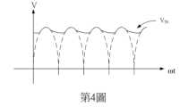
更詳言之,復參閱第3圖,其係本實施例之電壓擷取單元12將該交流電源AC轉換為之該直流擷取電壓VD後之波形圖。第4圖為該整流電路14依據該交流電源AC產生經整流之一直流輸入電源,該整流電路14通過該第一整流元件D1、該第二整流元件D2、該第三整流元件D3與該第四整流元件D4為等二極體及一輸入電容C蓄能作用,所產生之輸入電源的輸入電壓VIN第4圖所示之波形,並且輸出至該電源供應器18。由第3、4圖可看出該直流擷取電壓VD係相關於該整流電路14輸入至該電源供應器18之輸入電壓VIN,故可用來監測該輸入電壓VIN。In more detail, refer to FIG. 3 again, which is a waveform diagram of the DC voltage VD after the voltage capture unit 12 of the present embodiment converts the AC power source AC into a DC input power source. FIG. 4 shows that the rectifier circuit 14 generates a rectified DC input power source according to the AC power source AC. The rectifier circuit 14 generates an input power source through the first rectifier element D1, the second rectifier element D2, the third rectifier element D3 and the fourth rectifier element D4 as diodes and an input capacitor C for energy storage, and the input voltage VIN of the input power source is shown in FIG. 4, and is output to the power supply 18. It can be seen from FIGS. 3 and 4 that the DC extraction voltage VD is related to the input voltage VIN of the rectifier circuit 14 to the power supply 18 , and can therefore be used to monitor the input voltage VIN .
在本實施例的該電壓監測電路16中,該第一偵測電路162與該第二偵測電路164依據該分壓電壓VDIV偵測該輸入電壓VIN,因而讓該第一偵測電路162與該第二偵測電路164分別依據該分壓電壓VDIV、一第一門檻值Vth1與一第二門檻值Vth2產生一第一電壓訊號VT1或一第二電壓訊號VT2,其中,本實施例之該第一門檻值Vth1對應於該第一偵測電路162之一第一參考電流IREF1,該第二門檻值Vth2對應於該第二偵測電路164之一參考電壓VREF1。其中該第一參考電流IREF1與該參考電壓VREF1為該第一偵測電路162與該第二偵測電路164於IC電路設計製造時之預設參數值。該第一偵測電路162與該第二偵測電路164為較為可包含類比電路與邏輯運算電路。In the voltage monitoring circuit 16 of the present embodiment, the first detection circuit 162 and the second detection circuit 164 detect the input voltage VIN according to the divided voltage VDIV , so that the first detection circuit 162 and the second detection circuit 164 generate a first voltage signal VT1 or a second voltage signal VT2 according to the divided voltage VDIV , a first threshold value Vth1 and a second threshold value Vth2, respectively, wherein the first threshold value Vth1 of the present embodiment corresponds to a first reference current IREF1 of the first detection circuit 162, and the second threshold value Vth2 corresponds to a reference voltage VREF1 of the second detection circuit 164. The first reference current IREF1 and the reference voltage VREF1 are preset parameter values of the first detection circuit 162 and the second detection circuit 164 during IC circuit design and manufacturing. The first detection circuit 162 and the second detection circuit 164 may include analog circuits and logic operation circuits.
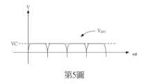
詳言之,在本實施例中當該分壓電壓VDIV超過一拑制門檻值VC(如第5圖所示)時,該第一偵測電路162拑制該分壓電壓VDIV,使該分壓電壓VDIV維持等於或接近該拑制門檻值VC,並依據流入該第一偵測電路162之一偵測電流IIN1的電流值偵測該輸入電壓VIN。其中,因為該壓電壓VDIV被拑制,當該交流電源AC電壓增加使該直流擷取電壓VD增加,流入該第一偵測電路162之偵測電流IIN1將隨之增加;反之當該交流電源AC電壓減少使該直流擷取電壓VD減少,流入該第一偵測電路162之偵測電流IIN1將隨之減少;故該偵測電流IIN1可用於判斷該交流電源AC及該輸入電壓VIN的大小。因此,當該第一偵測電路162依據該偵測電流的電流值判斷該輸入電壓VIN大於該第一門檻值Vth1時,該第一偵測電路162產生該第一電壓訊號VT1In detail, in this embodiment, when the divided voltage VDIV exceeds a control threshold VC (as shown in FIG. 5 ), the first detection circuit 162 controls the divided voltage VDIV so that the divided voltage VDIV is maintained equal to or close to the control threshold VC, and detects the input voltage VIN according to the current value of a detection current IIN1 flowing into the first detection circuit 162 . Among them, because the voltage VDIV is controlled, when the AC power source AC voltage increases, the DC extraction voltage VD increases, and the detection current IIN1 flowing into the first detection circuit 162 will increase accordingly; conversely, when the AC power source AC voltage decreases, the DC extraction voltage VD decreases, and the detection current IIN1 flowing into the first detection circuit 162 will decrease accordingly; therefore, the detection current IIN1 can be used to determine the size of the AC power source AC and the input voltage VIN . Therefore, when the first detection circuit 162 determines that the input voltage VIN is greater than the first threshold value Vth1 according to the current value of the detection current, the first detection circuit 162 generates the first voltage signal VT1.
一旦該直流擷取電壓VD減少至使該分壓電壓VDIV未超過該拑制門檻值VC,該第一偵測電路162將停止拑制該分壓電壓VDIV。該第二偵測電路164依據該分壓電壓VDIV偵測該輸入電壓VIN,當該第二偵測電路164依據該分壓電壓VDIV的電壓值判斷該輸入電壓VIN小於該第二門檻值Vth2時,該第二偵測電路164產生該第二電壓訊號VT2。Once the DC extraction voltage VD decreases to make the divided voltage VDIV no longer exceed the control threshold VC, the first detection circuit 162 stops controlling the divided voltage VDIV . The second detection circuit 164 detects the input voltage VIN according to the divided voltage VDIV . When the second detection circuit 164 determines that the input voltage VIN is less than the second threshold Vth2 according to the voltage value of the divided voltage VDIV , the second detection circuit 164 generates the second voltage signal VT2.
更詳言之,本實施例中,該第一偵測電路162包含一電流鏡1622、一參考電流源1624與一第一訊號處理單元1626,而該電流鏡1622包含一第一鏡像輸入單元M1IN與一第一鏡像輸出單元M1OUT,藉由該第一鏡像輸入端M1IN於該分壓電壓VDIV超過該拑制門檻值VC時拑制該分壓電壓VDIV,並接收一偵測電流IIN1至該第一鏡像輸入單元M1IN,且該第一鏡像輸出單元M1OUT對應輸出一第一鏡像電流IOUT1,本實施例之該參考電流源1624為提供該第一參考電流IREF1。該第一訊號處理單元1626為依據該第一參考電流IREF1與該第一鏡像電流IOUT1之電流值判斷該偵測電流IIN1的大小,進而判斷該輸入電壓VIN是否超過該第一門檻值Vth1,並在判斷該輸入電壓VIN大於該第一門檻值Vth1時,產生該第一電壓訊號VT1。其中,該偵測電流IIN1為該電流鏡1622之輸入電流,該第一鏡像電流IOUT1為該電流鏡1622之一輸出電流,且兩者呈倍數關係;換言之,該偵測電流IN1與該第一鏡像電流IOUT1之比例為K,即IN1:IOUT1= 1:K,可依據使用需求而調整。該拑制門檻值VC大於該第二偵測電路164所使用之一參考電壓VREF1(詳述如後),且當該分壓電壓VDIV小於該拑制門檻值VC時,該偵測電流IIN1之電流值理想為0。In more detail, in this embodiment, the first detection circuit 162 includes a current mirror 1622, a reference current source 1624 and a first signal processing unit 1626, and the current mirror 1622 includes a first mirror input unit M1IN and a first mirror output unit M1OUT . When the divided voltage VDIV exceeds the control threshold VC, the divided voltage VDIV is controlled by the first mirror input terminal M1IN , and a detection current IIN1 is received to the first mirror input unit M1IN , and the first mirror output unit M1OUT outputs a first mirror current IOUT1 in response. The reference current source 1624 of this embodiment provides the first reference current IREF1 . The first signal processing unit 1626 determines the magnitude of the detection current IIN1 according to the current values of the first reference current IREF1 and the first mirror current IOUT1 , and further determines whether the input voltage VIN exceeds the first threshold value Vth1, and generates the first voltage signal VT1 when it is determined that the input voltage VIN is greater than the first threshold value Vth1. The detection current IIN1 is the input current of the current mirror 1622, and the first mirror current IOUT1 is an output current of the current mirror 1622, and the two are in a multiple relationship; in other words, the ratio of the detection current IN1 to the first mirror current IOUT1 is K, that is, IN1 :IOUT1 = 1:K, which can be adjusted according to the use requirements. The control threshold value VC is greater than a reference voltage VREF1 used by the second detection circuit 164 (described in detail below), and when the voltage division voltage VDIV is less than the control threshold value VC, the current value of the detection current IIN1 is ideally 0.
在本實施例中,該第二偵測電路164包含一比較器1642與一第二訊號處理單元1644,該比較器1642包含一正輸入端與一負輸入端,該比較器1642透過該正輸入端耦接該參考電壓VREF1,並透過該負輸入端耦接該分壓電壓VDIV,因此,該比較器1642透過一輸出端產生一比較結果OUT至該第二訊號處理單元1644,使該第二訊號處理單元1644依據該比較結果OUT判斷該輸入電壓VIN是否小於該第二門檻值Vth2,並在判斷該輸入電壓VIN小於該第二門檻值Vth2時,產生該第二電壓訊號VT2。In this embodiment, the second detection circuit 164 includes a comparator 1642 and a second signal processing unit 1644. The comparator 1642 includes a positive input terminal and a negative input terminal. The comparator 1642 is coupled to the reference voltage VREF1 through the positive input terminal, and is coupled to the divided voltage VDIV through the negative input terminal. Therefore, the comparator 1642 generates a comparison result OUT through an output terminal to the second signal processing unit 1644, so that the second signal processing unit 1644 determines whether the input voltage V IN is less than the second threshold value V th2 according to the comparison result OUT, and determines whether the input voltage VIN is less than the second threshold value V th2. WhenIN is less than the second threshold value Vth2, the second voltage signal VT2 is generated.
此外,本實施例中,該電源供應器18依據該第一電壓訊號VT1執行一第一作動機制,例如: 該第一作動機制可以為一過壓保護、一高壓判斷或一輸入電壓切換;該電源供應器18依據該第二電壓訊號VT2執行一第二作動機制,例如: 該第二作動機制可以為一欠壓保護或一最低啟動電壓設定。In addition, in this embodiment, the power supply 18 executes a first actuation mechanism according to the first voltage signal VT1, for example: the first actuation mechanism can be an overvoltage protection, a high voltage judgment or an input voltage switching; the power supply 18 executes a second actuation mechanism according to the second voltage signal VT2, for example: the second actuation mechanism can be an undervoltage protection or a minimum starting voltage setting.
由以上所述可知,本發明之電壓監測電路16為利用該第一偵測電路162與該第二偵測電路164依據該分壓電壓VDIV偵測該輸入電壓VIN,因而讓該第一偵測電路162與該第二偵測電路164分別依據該分壓電壓VDIV、該第一門檻值Vth1與該第二門檻值Vth2產生該第一電壓訊號VT1或該第二電壓訊號VT2。同時,當該分壓電壓VDIV超過該拑制門檻值VC(如第5圖所示)時,該第一偵測電路162拑制該分壓電壓VDIV並依據該偵測電流IIN1的電流值偵測該輸入電壓VIN;該第二偵測電路164依據該分壓電壓VDIV偵測該輸入電壓VIN。藉此,該第一偵測電路162與該第二偵測電路164可用於偵測該輸入電壓VIN,且該第一偵測電路162與該第二偵測電路164可分開設定其參數。From the above description, it can be known that the voltage monitoring circuit 16 of the present invention utilizes the first detection circuit 162 and the second detection circuit 164 to detect the input voltage VIN according to the divided voltage VDIV , so that the first detection circuit 162 and the second detection circuit 164 generate the first voltage signal VT1 or the second voltage signal VT2 according to the divided voltage VDIV , the first threshold value Vth1 and the second threshold value Vth2 respectively. At the same time, when the divided voltage VDIV exceeds the control threshold VC (as shown in FIG. 5 ), the first detection circuit 162 controls the divided voltage VDIV and detects the input voltage VIN according to the current value of the detection current IIN1 ; the second detection circuit 164 detects the input voltage VIN according to the divided voltage VDIV . Thus, the first detection circuit 162 and the second detection circuit 164 can be used to detect the input voltage VIN , and the first detection circuit 162 and the second detection circuit 164 can set their parameters separately.
接續上述,如第6圖所示為構建該第一偵測電路162的一種細部電路範例,該第一鏡像輸入單元M1IN包含一運算放大器OP、一輸入電晶體M11與一第一鏡像電晶體M12,而該第一鏡像輸出單元M1OUT包含一第一輸出電晶體M13,藉由該運算放大器OP之一正輸入端耦合該拑制門檻值VC,該運算放大器OP之一負輸入端耦合該分壓電壓VDIV,因此在該分壓電壓VDIV未超過該拑制門檻值VC時,該輸入電晶體M11係截止使該第一偵測電路162不作用,此時該第一偵測電路162並不影響該分壓電壓VDIV;一旦該分壓電壓VDIV超過該拑制門檻值VC時,該運算放大器OP即控制該輸入電晶體M11導通該偵測電流IIN1,利用該運算放大器OP的虛短路特性拑制該分壓電壓VDIV使其維持等於或接近拑制門檻值VC,並利用該第一鏡像電晶體M12與該第一輸出電晶體M13形成之電流鏡,而產生該第一鏡像電流IOUT1,而該第一訊號處理單元1626即依據該第一參考電流IREF1與該第一鏡像電流IOUT1產生該第一電壓訊號VT1。Continuing with the above, as shown in FIG. 6, a detailed circuit example of constructing the first detection circuit 162 is shown. The first mirror input unit M1IN includes an operational amplifier OP, an input transistor M11 and a first mirror transistor M12, and the first mirror output unit M1OUT includes a first output transistor M13. A positive input terminal of the operational amplifier OP is coupled to the control threshold value VC, and a negative input terminal of the operational amplifier OP is coupled to the divided voltage VDIV . Therefore, when the divided voltage VDIV does not exceed the control threshold value VC, the input transistor M11 is turned off to make the first detection circuit 162 inactive. At this time, the first detection circuit 162 does not affect the divided voltage VDIV. Once the divided voltage VDIV exceeds the control threshold VC, the operational amplifier OP controls the input transistor M11 to conduct the detection current IIN1 , and utilizes the virtual short-circuit characteristic of the operational amplifier OP to control the divided voltage VDIV to maintain it equal to or close to the control threshold VC, and utilizes the current mirror formed by the first mirror transistor M12 and the first output transistor M13 to generate the first mirror current IOUT1 , and the first signal processing unit 1626 generates the first voltage signal VT1 according to the first reference current IREF1 and the first mirror current IOUT1 .
承上所述,本發明第一實施例電源供應器之電壓監測方法及其電路中,第一門檻值Vth1與該第二門檻值Vth2可以表示如下式所示:As mentioned above, in the voltage monitoring method and circuit of the power supply of the first embodiment of the present invention, the first threshold value Vth1 and the second threshold value Vth2 can be expressed as shown in the following formula:
以下舉一簡單數值範例,假設該第一門檻值Vth1與該第二門檻值Vth2分別希望設定為300VAC與80VAC,該第一參考電流IREF1選擇為50μA,該拑制門檻值VC選擇為1V,該第二參考電壓VREF1選擇為0.8V,該偵測電流IN1與該第一鏡像電流IOUT1之比例K選擇為1,上述通常均為IC電路設計製造時之預設參數值。然而第一阻抗元件ZU與該第二阻抗元件ZD一般是耦接於IC外部的元件,因此通過上式可以計算出在前述所選預設參數值下,該第一阻抗元件ZU與該第二阻抗元件ZD之阻抗值分別為5.656百萬歐姆(MΩ)與40.2849千歐姆(kΩ),能夠正確將該第一門檻值Vth1與該第二門檻值Vth2分別設定為300VAC與80VAC。The following is a simple numerical example. Assume that the first threshold value Vth1 and the second threshold value Vth2 are desired to be set to 300VAC and 80VAC respectively, the first reference current IREF1 is selected to be 50μA, the control threshold value VC is selected to be 1V, the second reference voltage VREF1 is selected to be 0.8V, and the ratio K of the detection current IN1 and the first mirror current IOUT1 is selected to be 1. The above are usually the default parameter values when the IC circuit is designed and manufactured. However, the first impedance element ZU and the second impedance element ZD are generally elements coupled to the outside of the IC. Therefore, the above formula can be used to calculate that under the aforementioned selected default parameter values, the impedance values of the first impedance element ZU and the second impedance element ZD are 5.656 million ohms (MΩ) and 40.2849 kiloohms (kΩ), respectively, which can correctly set the first threshold value Vth1 and the second threshold value Vth2 to 300VAC and 80VAC, respectively.
進一步地,假設該第一門檻值Vth1希望調整為250VAC,但式該第二門檻值Vth2仍希望維持為80VAC,在前述所選預設參數值都未變動的情況下,通過上式可以計算出該第一阻抗元件ZU與該第二阻抗元件ZD之阻抗值分別為4.1311百萬歐姆(MΩ)與29.4194千歐姆(kΩ),能夠在不影響該第二門檻值Vth2的前提下將該第一門檻值Vth1調整為250VAC。Furthermore, assuming that the first threshold value Vth1 is desired to be adjusted to 250VAC, but the second threshold value Vth2 is still desired to be maintained at 80VAC, under the condition that the aforementioned selected preset parameter values are not changed, the impedance values of the first impedance element ZU and the second impedance element ZD can be calculated by the above formula to be 4.1311 million ohms (MΩ) and 29.4194 kiloohms (kΩ), respectively, so that the first threshold value Vth1 can be adjusted to 250VAC without affecting the second threshold value Vth2.
因此,雖然本發明實施例同樣只用一分壓電壓節點來監測輸入電壓,卻可透過改變該第一阻抗元件ZU與該第二阻抗元件ZD之阻抗值,來完成該第一門檻值Vth1與該第二門檻值Vth2的獨立設定與調整,而且該第一門檻值Vth1與該第二門檻值Vth2彼此之間不存在相依的情況。本實施例該第一阻抗元件ZU與該第二阻抗元件ZD之阻抗值係單純以電阻值作為舉例說明,但不限於此,更可以利用電容或電感等其他元件來構成該第一阻抗元件ZU與該第二阻抗元件ZD。也就是說本發明更可利用該第一參考電流IREF1、該參考電壓VREF1、該第一阻抗元件ZU之一第一阻抗值與該第二阻抗元件ZD之一第二阻抗值共同設定或調整該第一門檻值Vth1與該第二門檻值Vth2。Therefore, although the embodiment of the present invention also uses only one voltage-dividing node to monitor the input voltage, the first threshold value Vth1 and the second threshold value Vth2 can be independently set and adjusted by changing the impedance values of the first impedance element ZU and the second impedance element ZD , and the first threshold value Vth1 and the second threshold value Vth2 do not depend on each other. In this embodiment, the impedance values of the first impedance element ZU and the second impedance element ZD are simply illustrated by resistance values, but are not limited to this. Other elements such as capacitors or inductors can also be used to constitute the first impedance element ZU and the second impedance element ZD. That is to say, the present invention can further utilize the first reference current IREF1 , the reference voltage VREF1 , a first impedance value of the first impedance element ZU , and a second impedance value of the second impedance element ZD to jointly set or adjust the first threshold value Vth1 and the second threshold value Vth2 .
如第7圖所示,其為本發明之第二實施例之電路示意圖。其中,第2圖與第7圖之差異在於 第2圖之電壓監測電路16耦接於一電壓擷取單元12,也就是耦接於該交流電源AC與該整流電路14之間,而第7圖之電壓監測電路16耦接於該整流電路14與該電源供應器18之間。由於本實施例之該分壓電路DIV為直接依據該輸入電壓VIN產生該分壓電壓VDIV,因此,本實施例之該分壓電壓VDIV為直接關聯於該輸入電壓VIN,且本實施例之電源供應裝置10A並未設置該電壓擷取單元12。As shown in FIG. 7, it is a circuit diagram of the second embodiment of the present invention. The difference between FIG. 2 and FIG. 7 is that the voltage monitoring circuit 16 of FIG. 2 is coupled to a voltage acquisition unit 12, that is, coupled between the alternating current power source AC and the rectifier circuit 14, while the voltage monitoring circuit 16 of FIG. 7 is coupled between the rectifier circuit 14 and the power supply 18. Since the voltage-dividing circuit DIV of this embodiment directly generates the divided voltage VDIV according to the input voltage VIN , the divided voltage VDIV of this embodiment is directly related to the input voltage VIN , and the power supply device 10A of this embodiment is not provided with the voltage acquisition unit 12.
於本實施例中,除了值接接收整流後的輸入電壓VIN來產生該分壓電壓VDIV有別於本發明之第一實施例,其餘訊號操作大致相同於該第一實施例,因此不再重複贅述。In this embodiment, except that the rectified input voltage VIN is received to generate the divided voltage VDIV , which is different from the first embodiment of the present invention, the rest of the signal operations are substantially the same as the first embodiment, and thus will not be repeated.
以上實施例為該第一偵測電路162依據該偵測電流IN1偵測該輸入電壓VIN是否大於第一門檻值Vth1,而該第二偵測電路164依據該分壓電壓VDIV偵測該輸入電壓VIN是否小於該第二門檻值Vth2,但本發明不限於此,更可將二者作用交換設置請參照第8圖,其為本發明另一實施例電源供應器之電壓監測方法的流程示意圖,其所使用的相關電路詳述如下:In the above embodiment, the first detection circuit 162 detects whether the input voltage VIN is greater than the first threshold value Vth1 according to the detection current IN1 , and the second detection circuit 164 detects whether the input voltage VIN is less than the second threshold value Vth2 according to the divided voltage VDIV , but the present invention is not limited thereto, and the two functions can be interchanged. Please refer to FIG. 8, which is a flow chart of a voltage monitoring method of a power supply according to another embodiment of the present invention, and the related circuits used are described in detail as follows:
如第9圖所示,其為本發明之第三實施例之電路示意圖。在前述實施例中,第一偵測電路162可通過該第一鏡像輸入單元M1IN之一輸入電晶體M11,來根據該分壓電壓VDIV的大小主動導通或截止該第一偵測電路162,惟在本實施例中該第一偵測電路162可進一步包含一開關元件SW,該開關元件SW可受該第一訊號處理單元VT1之控制而決定是否導通一偵測電流IIN2。另一方面,本實施例之該電流鏡1622為包含一第二鏡像輸入單元M2IN與一第二鏡像輸出單元M2OUT,且本實施例之該參考電流源1624為提供一第二參考電流IREF2,當該分壓電壓VDIV未超過該拑制門檻值VC時,該開關元件SW導通並拑制該分壓電壓VDIV,因而導通一偵測電流IIN2至該第二電流鏡1646,該第二電流鏡1646中包含一第一鏡像輸入單元M2IN與一第二鏡像輸出單元M2OUT,該第一鏡像輸入單元M2IN接收該偵測電流IIN2,同理,該第二鏡像輸出單元M2OUT產生對應之一第二鏡像電流IOUT2,該第一訊號處理單元1626即依據該第二參考電流IREF2以及該第二鏡像電流IOUT2判斷該輸入電壓VIN是否小於該第一門檻值Vth1,當該第一訊號處理單元1626判斷該輸入電壓VIN小於該第二門檻值時產生該第一電壓訊號VT1,此時如第10圖所示,本實施例之該第一門檻值Vth1為較低之門檻值。As shown in FIG. 9, it is a circuit diagram of the third embodiment of the present invention. In the aforementioned embodiment, the first detection circuit 162 can be actively turned on or off according to the magnitude of the divided voltage VDIV through an input transistor M11 of the first mirror input unit M1IN , but in this embodiment, the first detection circuit 162 can further include a switch element SW, and the switch element SW can be controlled by the first signal processing unit VT1 to determine whether to conduct a detection current IIN2 . On the other hand, the current mirror 1622 of the present embodiment includes a second mirror input unit M2IN and a second mirror output unit M2OUT , and the reference current source 1624 of the present embodiment provides a second reference current IREF2 . When the divided voltage VDIV does not exceed the control threshold VC, the switch element SW is turned on and controls the divided voltage VDIV , thereby conducting a detection current IIN2 to the second current mirror 1646. The second current mirror 1646 includes a first mirror input unit M2IN and a second mirror output unit M2OUT . The first mirror input unit M2IN receives the detection current IIN2 . Similarly, the second mirror output unit M2OUT generates a corresponding second mirror current IOUT2 . The first signal processing unit 1626 determines whether the input voltage VIN is less than the first threshold value Vth1 according to the second reference current IREF2 and the second mirror current IOUT2 . When the first signal processing unit 1626 determines that the input voltage VIN is less than the second threshold value, the first voltage signal VT1 is generated. At this time, as shown in FIG. 10, the first threshold value Vth1 of this embodiment is a lower threshold value.
一旦該直流擷取電壓VD增加至使該分壓電壓VDIV超過該拑制門檻值VC,該開關元件S截止,故該第一偵測電路162將停止拑制該分壓電壓VDIV。本實施例之該第二偵測電路164為接收該分壓電壓VDIV,藉此該比較器1642依據一參考電壓VREF2與該分壓電壓VDIV,而產生一比較結果OUT至該第二訊號處理單元1644,使該第二訊號處理單元1644依據該比較結果OUT判斷該輸入電壓VIN是否大於該第二門檻值Vth2,並在判斷該輸入電壓VIN大於該第二門檻值Vth2時,因而讓該第二訊號處理單元1644產生該第二電壓訊號VT2。本實施例之該第二門檻值Vth2大於該第一門檻值Vth1,因此本實施例相當於利用該第一偵測電路162依據較低之電壓門檻Vth1偵測該輸入電壓VIN,並利用該第二偵測電路164依據較高之電壓門檻Vth2偵測該輸入電壓VIN。Once the DC extraction voltage VD increases to make the divided voltage VDIV exceed the control threshold VC, the switch element S is turned off, so the first detection circuit 162 stops controlling the divided voltage VDIV . The second detection circuit 164 of the present embodiment receives the divided voltage VDIV , whereby the comparator 1642 generates a comparison result OUT to the second signal processing unit 1644 according to a reference voltage VREF2 and the divided voltage VDIV , so that the second signal processing unit 1644 determines whether the input voltage VIN is greater than the second threshold value Vth2 according to the comparison result OUT, and when it is determined that the input voltage VIN is greater than the second threshold value Vth2, the second signal processing unit 1644 generates the second voltage signal VT2. The second threshold value Vth2 of the present embodiment is greater than the first threshold value Vth1. Therefore, the present embodiment is equivalent to using the first detection circuit 162 to detect the input voltage VIN according to the lower voltage threshold Vth1, and using the second detection circuit 164 to detect the input voltage VIN according to the higher voltage threshold Vth2.
如第11圖所示,其為本發明之第四實施例之電路示意圖。本實施例之該分壓電路DIV改為耦接於該整流電路14與該電源供應器18之間,其餘連接關係同於上一實施例,因此不再贅述。As shown in FIG. 11 , which is a circuit diagram of the fourth embodiment of the present invention, the voltage divider circuit DIV of this embodiment is coupled between the rectifier circuit 14 and the power supply 18 , and the remaining connection relationship is the same as the previous embodiment, so it will not be repeated.
同理,在本發明第三實施例與第四實施例中,電壓監測電路16於設定或調整該第一門檻值Vth1或該第二門檻值Vth2時,可透過改變該第一阻抗元件ZU與該第二阻抗元件ZD之阻抗值來獨立設定與調整該第一門檻值Vth1或該第二門檻值Vth2,而且該第一門檻值Vth1與該第二門檻值Vth2彼此之間不存在相依的情況。本實施例該第一阻抗元件ZU與該第二阻抗元件ZD之阻抗值係單純以電阻值作為舉例說明,但不限於此,更可以利用電容或電感等其他元件來構成該第一阻抗元件ZU與該第二阻抗元件ZD。也就是說本發明更可利用該參考電壓VREF2、該第二參考電流IREF2、該第一阻抗元件ZU之一第一阻抗值與該第二阻抗元件ZD之一第二阻抗值共同設定或調整該第一門檻值Vth1與該第二門檻值Vth2。Similarly, in the third and fourth embodiments of the present invention, the voltage monitoring circuit 16 can independently set and adjust the first threshold value Vth1 or the second threshold value Vth2 by changing the impedance value of the first impedance element ZU and the second impedance element ZD when setting or adjusting the first threshold value Vth1 or the second threshold value Vth2, and the first threshold value Vth1 and the second threshold value Vth2 do not depend on each other. In this embodiment, the impedance value of the first impedance element ZU and the second impedance element ZD is simply illustrated by the resistance value, but it is not limited to this. Other elements such as capacitors or inductors can also be used to constitute the first impedance element ZU and the second impedance element ZD. That is to say, the present invention can further utilize the reference voltage VREF2 , the second reference current IREF2 , a first impedance value of the first impedance element ZU , and a second impedance value of the second impedance element ZD to jointly set or adjust the first threshold value Vth1 and the second threshold value Vth2 .
故本發明實為一具有新穎性、進步性及可供產業上利用者,應符合我國專利法專利申請要件無疑,爰依法提出發明專利申請,祈 鈞局早日賜准專利,至感為禱。Therefore, this invention is novel, progressive and can be used in the industry. It should undoubtedly meet the patent application requirements of the Patent Law of our country. Therefore, we have filed an invention patent application in accordance with the law and pray that the Bureau will approve the patent as soon as possible. I am deeply grateful.
惟以上所述者,僅為本發明之較佳實施例而已,並非用來限定本發明實施之範圍,舉凡依本發明申請專利範圍所述之形狀、構造、特徵及精神所為之均等變化與修飾,均應包括於本發明之申請專利範圍內。However, the above is only a preferred embodiment of the present invention and is not intended to limit the scope of implementation of the present invention. All equivalent changes and modifications made according to the shape, structure, features and spirit described in the patent application scope of the present invention should be included in the patent application scope of the present invention.
10:電源供應裝置 12:電壓擷取單元 122:第一二極體 124:第二二極體 14:整流電路 16:電壓監測電路 162:第一偵測電路 1622:電流鏡 1624:參考電流源 1626:第一訊號處理單元 164:第二偵測電路 1642:比較器 1644:第二訊號處理單元 18:電源供應器 AC:交流電源 C:輸入電容 D1:第一整流元件 D2:第二整流元件 D3:第三整流元件 D4:第四整流元件 DIV:分壓電路 IIN1:拑制電流 IIN2:拑制電流 IOUT1:第一鏡像電流 IOUT2:第二鏡像電流 IREF1:第一參考電流 IREF2:第二參考電流 M11:第一輸入電晶體 M12:第一鏡像電晶體 M13:第一輸出電晶體 M1IN:第一鏡像輸入單元 M1OUT:第一鏡像輸出單元 M2IN:第二鏡像輸入單元 M2OUT:第二鏡像輸出單元 OUT:比較結果 OP:運算放大器 SW:開關元件 VIN:輸入電壓 VD:直流擷取電壓 VDIV:分壓 VOUT:輸出電壓 VREF1:參考電壓 VREF2:參考電壓 VT1:第一電壓訊號 VT2:第二電壓訊號 ZU:第一阻抗元件 ZD:第二阻抗元件 1:K:比例10: power supply device 12: voltage acquisition unit 122: first diode 124: second diode 14: rectifier circuit 16: voltage monitoring circuit 162: first detection circuit 1622: current mirror 1624: reference current source 1626: first signal processing unit 164: second detection circuit 1642: comparator 1644: second signal processing unit 18: power supply AC: alternating current source C: input capacitor D1: first rectifier element D2: second rectifier element D3: third rectifier element D4: fourth rectifier element DIV: voltage divider circuit IIN1 : manipulation current IIN2 : manipulation current IOUT1 : first mirror current IOUT2 : second mirror current IREF1 : First reference current IREF2 : Second reference current M11: First input transistor M12: First mirror transistor M13: First output transistor M1IN : First mirror input unit M1OUT : First mirror output unit M2IN : Second mirror input unit M2OUT : Second mirror output unit OUT: Comparison result OP: Operational amplifier SW: Switching element VIN : Input voltage VD : DC extraction voltage VDIV : Divided voltage VOUT : Output voltage VREF1 : Reference voltage VREF2 : Reference voltage VT1: First voltage signal VT2: Second voltage signal ZU : First impedance element ZD : Second impedance element 1: K: Ratio
第1圖:其為本發明一實施例電源供應器之電壓監測方法的流程示意圖; 第2圖:其為本發明之第一實施例之電路示意圖; 第3圖:其為本發明之第一實施例之電壓擷取單元輸出端之訊號示意圖; 第4圖:其為本發明之輸入至電源供應器之輸入電壓之訊號示意圖; 第5圖:其為本發明之分壓電壓受到拑制之訊號示意圖; 第6圖:其為本發明之第一實施例之偵測電路的細部電路範例示意圖; 第7圖:其為本發明之第二實施例之電路示意圖; 第8圖:其為本發明另一實施例電源供應器之電壓監測方法的流程示意圖;第9圖:其為本發明之第三實施例之電路示意圖; 第10圖:其為本發明之第三實施例之整流電路輸出端之訊號示意圖;以及 第11圖:其為本發明之第四實施例之電路示意圖。Figure 1: It is a flow chart of the voltage monitoring method of the power supply of an embodiment of the present invention;Figure 2: It is a circuit diagram of the first embodiment of the present invention;Figure 3: It is a signal diagram of the output end of the voltage acquisition unit of the first embodiment of the present invention;Figure 4: It is a signal diagram of the input voltage input to the power supply of the present invention;Figure 5: It is a signal diagram of the divided voltage of the present invention being controlled;Figure 6: It is a detailed circuit example diagram of the detection circuit of the first embodiment of the present invention;Figure 7: It is a circuit diagram of the second embodiment of the present invention;Figure 8: It is a flow chart of a voltage monitoring method of a power supply of another embodiment of the present invention; Figure 9: It is a circuit diagram of the third embodiment of the present invention;Figure 10: It is a signal diagram of the output end of the rectifier circuit of the third embodiment of the present invention; andFigure 11: It is a circuit diagram of the fourth embodiment of the present invention.
10:電源供應裝置10: Power supply device
12:電壓擷取單元12: Voltage acquisition unit
122:第一二極體122: The first diode
124:第二二極體124: Second Diode
14:整流電路14: Rectifier circuit
16:電壓監測電路16: Voltage monitoring circuit
162:第一偵測電路162: First detection circuit
1622:電流鏡1622:Galvano mirror
1624:參考電流源1624: Reference current source
1626:第一訊號處理單元1626: First signal processing unit
164:第二偵測電路164: Second detection circuit
1642:比較器1642: Comparator
1644:第二訊號處理單元1644: Second signal processing unit
18:電源供應器18: Power supply
AC:交流電源AC: alternating current power
C:輸入電容C: Input capacitance
D1:第一整流元件D1: first rectifier element
D2:第二整流元件D2: Second rectifier element
D3:第三整流元件D3: The third rectifier element
D4:第四整流元件D4: The fourth rectifier element
DIV:分壓電路DIV: voltage divider circuit
IIN1:拑制電流IIN1 : Control current
IOUT1:第一鏡像電流IOUT1 : First image current
IREF1:第一參考電流IREF1 : First reference current
M1IN:第一鏡像輸入單元M1IN : First mirror input unit
M1OUT:第一鏡像輸出單元M1OUT : First mirror output unit
OUT:比較結果OUT: Comparison results
VD:直流擷取電壓VD : DC extraction voltage
VIN:輸入電壓VIN : Input voltage
VDIV:分壓VDIV : voltage divider
VOUT:輸出電壓VOUT : Output voltage
VREF1:參考電壓VREF1 : Reference voltage
VT1:第一電壓訊號VT1: first voltage signal
VT2:第二電壓訊號VT2: Second voltage signal
ZU:第一阻抗元件ZU : First impedance element
ZD:第二阻抗元件ZD : Second impedance element
1:K:比例1: K: ratio
Claims (22)
Translated fromChineseApplications Claiming Priority (2)
| Application Number | Priority Date | Filing Date | Title |
|---|---|---|---|
| US202163247487P | 2021-09-23 | 2021-09-23 | |
| US63/247,487 | 2021-09-23 |
Publications (2)
| Publication Number | Publication Date |
|---|---|
| TW202314442A TW202314442A (en) | 2023-04-01 |
| TWI852096Btrue TWI852096B (en) | 2024-08-11 |
Family
ID=85661119
Family Applications (3)
| Application Number | Title | Priority Date | Filing Date |
|---|---|---|---|
| TW111136261ATWI852096B (en) | 2021-09-23 | 2022-09-23 | Method and circuit for monitoring voltage of power supply |
| TW111136265ATWI822358B (en) | 2021-09-23 | 2022-09-23 | Method and circuit for monitoring power supply |
| TW111136127ATWI852095B (en) | 2021-09-23 | 2022-09-23 | Synchronous rectification circuit |
Family Applications After (2)
| Application Number | Title | Priority Date | Filing Date |
|---|---|---|---|
| TW111136265ATWI822358B (en) | 2021-09-23 | 2022-09-23 | Method and circuit for monitoring power supply |
| TW111136127ATWI852095B (en) | 2021-09-23 | 2022-09-23 | Synchronous rectification circuit |
Country Status (3)
| Country | Link |
|---|---|
| US (3) | US11835592B2 (en) |
| CN (3) | CN115856407A (en) |
| TW (3) | TWI852096B (en) |
Families Citing this family (2)
| Publication number | Priority date | Publication date | Assignee | Title |
|---|---|---|---|---|
| TWI852096B (en)* | 2021-09-23 | 2024-08-11 | 極創電子股份有限公司 | Method and circuit for monitoring voltage of power supply |
| CN118641989B (en)* | 2023-03-13 | 2025-03-28 | 北京有竹居网络技术有限公司 | Device, method and electronic circuit for monitoring power supply voltage of electronic circuit |
Citations (5)
| Publication number | Priority date | Publication date | Assignee | Title |
|---|---|---|---|---|
| US20020000844A1 (en)* | 2000-06-28 | 2002-01-03 | Nec Corporation | Comparator and a control circuit for a power MOSFET |
| TW201316658A (en)* | 2011-10-14 | 2013-04-16 | Infinno Technology Corp | Control circuit of power supply |
| TWI574494B (en)* | 2016-04-19 | 2017-03-11 | 群光電能科技股份有限公司 | Input-voltage-off detection apparatus and power supply with input-voltage-off detection apparatus |
| TWI579576B (en)* | 2015-10-21 | 2017-04-21 | 佳世達科技股份有限公司 | Alternating current detecting apparatus |
| TWI618342B (en)* | 2016-09-26 | 2018-03-11 | 通嘉科技股份有限公司 | Line-voltage detection circuit and relevant detection method |
Family Cites Families (29)
| Publication number | Priority date | Publication date | Assignee | Title |
|---|---|---|---|---|
| WO2005069469A1 (en)* | 2004-01-14 | 2005-07-28 | Sanken Electric Co., Ltd. | Dc-dc converter |
| JP4507918B2 (en)* | 2005-03-01 | 2010-07-21 | 富士電機システムズ株式会社 | Single power supply voltage measurement circuit |
| JP5169498B2 (en)* | 2008-06-02 | 2013-03-27 | 株式会社リコー | Current detection circuit and switching regulator including the current detection circuit |
| JP5287030B2 (en)* | 2008-08-20 | 2013-09-11 | 株式会社リコー | DC-DC converter and control method |
| US8810078B2 (en)* | 2008-12-26 | 2014-08-19 | Mitsubishi Electric Corporation | Analog current output circuit |
| CN102044978B (en)* | 2009-10-16 | 2014-07-23 | 群康科技(深圳)有限公司 | Power supply circuit and monitoring protection method thereof |
| US8450676B2 (en)* | 2009-12-12 | 2013-05-28 | Iptronics A/S | Optical receiver |
| CN102109550B (en)* | 2009-12-25 | 2013-04-17 | 台达电子工业股份有限公司 | Over-voltage and over-temperature detection circuit |
| US8649129B2 (en)* | 2010-11-05 | 2014-02-11 | System General Corporation | Method and apparatus of providing over-temperature protection for power converters |
| CN102759653A (en)* | 2011-04-28 | 2012-10-31 | 鸿富锦精密工业(深圳)有限公司 | Voltage detecting circuit |
| TWI487255B (en)* | 2012-07-13 | 2015-06-01 | Power Forest Technology Corp | Flyback-based power conversion apparatus and power conversion method thereof |
| CN103532102B (en) | 2013-09-26 | 2017-10-17 | 昂宝电子(上海)有限公司 | System and method for the overheat protector and overvoltage protection of power converting system |
| EP2869447A1 (en) | 2013-10-31 | 2015-05-06 | Dialog Semiconductor GmbH | Continuous comparator with improved calibration |
| TWI568160B (en)* | 2014-05-09 | 2017-01-21 | 立錡科技股份有限公司 | Flyback power converter and control circuit thereof |
| TWI521853B (en)* | 2014-12-24 | 2016-02-11 | 力林科技股份有限公司 | Power conversion device based on reverse architecture |
| US9966867B2 (en) | 2015-06-18 | 2018-05-08 | Semiconductor Components Industries, Llc | Dead time compensation for synchronous rectifiers in adaptive output powers |
| US10033268B2 (en)* | 2015-07-10 | 2018-07-24 | Micron Technology, Inc. | Apparatuses and methods for charge pump regulation |
| CN111490682A (en)* | 2016-04-08 | 2020-08-04 | 昂宝电子(上海)有限公司 | Flyback power supply system |
| JP6906182B2 (en)* | 2016-09-07 | 2021-07-21 | パナソニックIpマネジメント株式会社 | Power storage system |
| US10063159B1 (en) | 2017-06-30 | 2018-08-28 | Dialog Semiconductor Inc. | Adaptive synchronous rectifier sensing deglitch |
| CN107979289A (en)* | 2017-11-27 | 2018-05-01 | 成都芯源系统有限公司 | Synchronous rectification switching power supply circuit and control method thereof |
| JP2019168754A (en)* | 2018-03-22 | 2019-10-03 | 東芝メモリ株式会社 | Memory system |
| JP7003003B2 (en)* | 2018-06-21 | 2022-01-20 | ルネサスエレクトロニクス株式会社 | Power circuit |
| CN109067183B (en)* | 2018-08-28 | 2020-10-20 | 佛山市南海赛威科技技术有限公司 | Switching power supply chip, its pin multiplexing circuit, and pin multiplexing method |
| CN210092865U (en)* | 2019-07-28 | 2020-02-18 | 田村电子(深圳)有限公司 | Switching power supply over-temperature protection circuit |
| US11682969B2 (en)* | 2019-12-13 | 2023-06-20 | Texas Instruments Incorporated | Voltage regulator with on-time extension |
| US11146176B2 (en) | 2020-02-28 | 2021-10-12 | Astec International Limited | Switch-mode power supplies including three-level LLC circuits |
| CN113315093B (en)* | 2021-05-27 | 2023-07-25 | 富满微电子集团股份有限公司 | Overvoltage and overtemperature protection circuit, chip and system |
| TWI852096B (en)* | 2021-09-23 | 2024-08-11 | 極創電子股份有限公司 | Method and circuit for monitoring voltage of power supply |
- 2022
- 2022-09-23TWTW111136261Apatent/TWI852096B/enactive
- 2022-09-23USUS17/934,744patent/US11835592B2/enactiveActive
- 2022-09-23USUS17/951,597patent/US12352823B2/enactiveActive
- 2022-09-23CNCN202211168058.8Apatent/CN115856407A/enactivePending
- 2022-09-23TWTW111136265Apatent/TWI822358B/enactive
- 2022-09-23CNCN202211168355.2Apatent/CN115902360A/enactivePending
- 2022-09-23CNCN202211166049.5Apatent/CN115864867A/enactivePending
- 2022-09-23USUS17/951,616patent/US12235329B2/enactiveActive
- 2022-09-23TWTW111136127Apatent/TWI852095B/enactive
Patent Citations (5)
| Publication number | Priority date | Publication date | Assignee | Title |
|---|---|---|---|---|
| US20020000844A1 (en)* | 2000-06-28 | 2002-01-03 | Nec Corporation | Comparator and a control circuit for a power MOSFET |
| TW201316658A (en)* | 2011-10-14 | 2013-04-16 | Infinno Technology Corp | Control circuit of power supply |
| TWI579576B (en)* | 2015-10-21 | 2017-04-21 | 佳世達科技股份有限公司 | Alternating current detecting apparatus |
| TWI574494B (en)* | 2016-04-19 | 2017-03-11 | 群光電能科技股份有限公司 | Input-voltage-off detection apparatus and power supply with input-voltage-off detection apparatus |
| TWI618342B (en)* | 2016-09-26 | 2018-03-11 | 通嘉科技股份有限公司 | Line-voltage detection circuit and relevant detection method |
Also Published As
| Publication number | Publication date |
|---|---|
| CN115856407A (en) | 2023-03-28 |
| CN115902360A (en) | 2023-04-04 |
| TW202314443A (en) | 2023-04-01 |
| US12235329B2 (en) | 2025-02-25 |
| US11835592B2 (en) | 2023-12-05 |
| CN115864867A (en) | 2023-03-28 |
| US12352823B2 (en) | 2025-07-08 |
| US20230160973A1 (en) | 2023-05-25 |
| TWI852095B (en) | 2024-08-11 |
| US20230216419A1 (en) | 2023-07-06 |
| US20230168312A1 (en) | 2023-06-01 |
| TW202315292A (en) | 2023-04-01 |
| TW202314442A (en) | 2023-04-01 |
| TWI822358B (en) | 2023-11-11 |
Similar Documents
| Publication | Publication Date | Title |
|---|---|---|
| TWI852096B (en) | Method and circuit for monitoring voltage of power supply | |
| CN101159410B (en) | Control circuit method and apparatus responsive to impedance coupled to control circuit terminals | |
| CN101572487B (en) | Semiconductor device for controlling switching power supply | |
| TWI393333B (en) | Controller chip and protection method for a power converter | |
| KR101754111B1 (en) | Adaptive overvoltage protection circuit and method, and power system including the same | |
| TWI321272B (en) | Power factor correction circuit and controlling method of output voltage thereof | |
| TW201347371A (en) | Discharge circuit and discharge method for EMI filtering capacitor | |
| TW201203819A (en) | A start-up circuit with low standby power loss for power converters | |
| TWI646767B (en) | Power control device and power control system | |
| TW201937331A (en) | Voltage regulation system, voltage regulation chip and voltage regulation control method thereof | |
| CN109792391B (en) | MPS generation system and method | |
| CN105576999B (en) | Input voltage detection circuit and parameter setting and circuit protection method thereof | |
| JP2014117045A (en) | Charge pump circuit | |
| US20200144914A1 (en) | Detection method, detection circuit, controller and switching power supply | |
| TWI678876B (en) | Alternator and rectifier thereof | |
| TWM580684U (en) | Load status detecting device | |
| TW202037055A (en) | Load condition detection apparatus including a detection unit, a rectifying and filtering unit, an amplifying unit and a comparing unit | |
| TWI717838B (en) | Power supply device | |
| JP2019009947A (en) | Switching power supply device | |
| TWI750170B (en) | Dc-to-dc controller, dc-to-dc power converter and control method thereof | |
| WO2015157857A1 (en) | Power supply circuit with active under-voltage protection | |
| TWI862023B (en) | Detection device and detection method thereof | |
| TWI845426B (en) | Controller for controlling blocking switch of power converter | |
| CN113765415B (en) | buck converter | |
| JP4853253B2 (en) | Power supply circuit with input disconnection detection function |