TWI850976B - Electronic package, package substrate and fabricating method thereof - Google Patents
Electronic package, package substrate and fabricating method thereofDownload PDFInfo
- Publication number
- TWI850976B TWI850976BTW112102059ATW112102059ATWI850976BTW I850976 BTWI850976 BTW I850976BTW 112102059 ATW112102059 ATW 112102059ATW 112102059 ATW112102059 ATW 112102059ATW I850976 BTWI850976 BTW I850976B
- Authority
- TW
- Taiwan
- Prior art keywords
- layer
- wiring
- circuit
- dielectric layer
- insulating layer
- Prior art date
Links
Images


Classifications
- H—ELECTRICITY
- H01—ELECTRIC ELEMENTS
- H01L—SEMICONDUCTOR DEVICES NOT COVERED BY CLASS H10
- H01L23/00—Details of semiconductor or other solid state devices
- H01L23/48—Arrangements for conducting electric current to or from the solid state body in operation, e.g. leads, terminal arrangements ; Selection of materials therefor
- H01L23/488—Arrangements for conducting electric current to or from the solid state body in operation, e.g. leads, terminal arrangements ; Selection of materials therefor consisting of soldered or bonded constructions
- H01L23/498—Leads, i.e. metallisations or lead-frames on insulating substrates, e.g. chip carriers
- H01L23/49811—Additional leads joined to the metallisation on the insulating substrate, e.g. pins, bumps, wires, flat leads
- H—ELECTRICITY
- H01—ELECTRIC ELEMENTS
- H01L—SEMICONDUCTOR DEVICES NOT COVERED BY CLASS H10
- H01L21/00—Processes or apparatus adapted for the manufacture or treatment of semiconductor or solid state devices or of parts thereof
- H01L21/02—Manufacture or treatment of semiconductor devices or of parts thereof
- H01L21/04—Manufacture or treatment of semiconductor devices or of parts thereof the devices having potential barriers, e.g. a PN junction, depletion layer or carrier concentration layer
- H01L21/48—Manufacture or treatment of parts, e.g. containers, prior to assembly of the devices, using processes not provided for in a single one of the groups H01L21/18 - H01L21/326 or H10D48/04 - H10D48/07
- H01L21/4814—Conductive parts
- H01L21/4846—Leads on or in insulating or insulated substrates, e.g. metallisation
- H01L21/4853—Connection or disconnection of other leads to or from a metallisation, e.g. pins, wires, bumps
- H—ELECTRICITY
- H01—ELECTRIC ELEMENTS
- H01L—SEMICONDUCTOR DEVICES NOT COVERED BY CLASS H10
- H01L21/00—Processes or apparatus adapted for the manufacture or treatment of semiconductor or solid state devices or of parts thereof
- H01L21/02—Manufacture or treatment of semiconductor devices or of parts thereof
- H01L21/04—Manufacture or treatment of semiconductor devices or of parts thereof the devices having potential barriers, e.g. a PN junction, depletion layer or carrier concentration layer
- H01L21/48—Manufacture or treatment of parts, e.g. containers, prior to assembly of the devices, using processes not provided for in a single one of the groups H01L21/18 - H01L21/326 or H10D48/04 - H10D48/07
- H01L21/4814—Conductive parts
- H01L21/4846—Leads on or in insulating or insulated substrates, e.g. metallisation
- H01L21/4857—Multilayer substrates
- H—ELECTRICITY
- H01—ELECTRIC ELEMENTS
- H01L—SEMICONDUCTOR DEVICES NOT COVERED BY CLASS H10
- H01L23/00—Details of semiconductor or other solid state devices
- H01L23/48—Arrangements for conducting electric current to or from the solid state body in operation, e.g. leads, terminal arrangements ; Selection of materials therefor
- H01L23/488—Arrangements for conducting electric current to or from the solid state body in operation, e.g. leads, terminal arrangements ; Selection of materials therefor consisting of soldered or bonded constructions
- H01L23/498—Leads, i.e. metallisations or lead-frames on insulating substrates, e.g. chip carriers
- H01L23/49811—Additional leads joined to the metallisation on the insulating substrate, e.g. pins, bumps, wires, flat leads
- H01L23/49816—Spherical bumps on the substrate for external connection, e.g. ball grid arrays [BGA]
- H—ELECTRICITY
- H01—ELECTRIC ELEMENTS
- H01L—SEMICONDUCTOR DEVICES NOT COVERED BY CLASS H10
- H01L23/00—Details of semiconductor or other solid state devices
- H01L23/48—Arrangements for conducting electric current to or from the solid state body in operation, e.g. leads, terminal arrangements ; Selection of materials therefor
- H01L23/488—Arrangements for conducting electric current to or from the solid state body in operation, e.g. leads, terminal arrangements ; Selection of materials therefor consisting of soldered or bonded constructions
- H01L23/498—Leads, i.e. metallisations or lead-frames on insulating substrates, e.g. chip carriers
- H01L23/49822—Multilayer substrates
- H—ELECTRICITY
- H01—ELECTRIC ELEMENTS
- H01L—SEMICONDUCTOR DEVICES NOT COVERED BY CLASS H10
- H01L23/00—Details of semiconductor or other solid state devices
- H01L23/48—Arrangements for conducting electric current to or from the solid state body in operation, e.g. leads, terminal arrangements ; Selection of materials therefor
- H01L23/488—Arrangements for conducting electric current to or from the solid state body in operation, e.g. leads, terminal arrangements ; Selection of materials therefor consisting of soldered or bonded constructions
- H01L23/498—Leads, i.e. metallisations or lead-frames on insulating substrates, e.g. chip carriers
- H01L23/49827—Via connections through the substrates, e.g. pins going through the substrate, coaxial cables
- H—ELECTRICITY
- H01—ELECTRIC ELEMENTS
- H01L—SEMICONDUCTOR DEVICES NOT COVERED BY CLASS H10
- H01L23/00—Details of semiconductor or other solid state devices
- H01L23/48—Arrangements for conducting electric current to or from the solid state body in operation, e.g. leads, terminal arrangements ; Selection of materials therefor
- H01L23/488—Arrangements for conducting electric current to or from the solid state body in operation, e.g. leads, terminal arrangements ; Selection of materials therefor consisting of soldered or bonded constructions
- H01L23/498—Leads, i.e. metallisations or lead-frames on insulating substrates, e.g. chip carriers
- H01L23/49838—Geometry or layout
- H—ELECTRICITY
- H01—ELECTRIC ELEMENTS
- H01L—SEMICONDUCTOR DEVICES NOT COVERED BY CLASS H10
- H01L2224/00—Indexing scheme for arrangements for connecting or disconnecting semiconductor or solid-state bodies and methods related thereto as covered by H01L24/00
- H01L2224/01—Means for bonding being attached to, or being formed on, the surface to be connected, e.g. chip-to-package, die-attach, "first-level" interconnects; Manufacturing methods related thereto
- H01L2224/10—Bump connectors; Manufacturing methods related thereto
- H01L2224/15—Structure, shape, material or disposition of the bump connectors after the connecting process
- H01L2224/16—Structure, shape, material or disposition of the bump connectors after the connecting process of an individual bump connector
- H01L2224/161—Disposition
- H01L2224/16135—Disposition the bump connector connecting between different semiconductor or solid-state bodies, i.e. chip-to-chip
- H01L2224/16145—Disposition the bump connector connecting between different semiconductor or solid-state bodies, i.e. chip-to-chip the bodies being stacked
- H—ELECTRICITY
- H01—ELECTRIC ELEMENTS
- H01L—SEMICONDUCTOR DEVICES NOT COVERED BY CLASS H10
- H01L2224/00—Indexing scheme for arrangements for connecting or disconnecting semiconductor or solid-state bodies and methods related thereto as covered by H01L24/00
- H01L2224/01—Means for bonding being attached to, or being formed on, the surface to be connected, e.g. chip-to-package, die-attach, "first-level" interconnects; Manufacturing methods related thereto
- H01L2224/10—Bump connectors; Manufacturing methods related thereto
- H01L2224/15—Structure, shape, material or disposition of the bump connectors after the connecting process
- H01L2224/16—Structure, shape, material or disposition of the bump connectors after the connecting process of an individual bump connector
- H01L2224/161—Disposition
- H01L2224/16151—Disposition the bump connector connecting between a semiconductor or solid-state body and an item not being a semiconductor or solid-state body, e.g. chip-to-substrate, chip-to-passive
- H01L2224/16221—Disposition the bump connector connecting between a semiconductor or solid-state body and an item not being a semiconductor or solid-state body, e.g. chip-to-substrate, chip-to-passive the body and the item being stacked
- H01L2224/16225—Disposition the bump connector connecting between a semiconductor or solid-state body and an item not being a semiconductor or solid-state body, e.g. chip-to-substrate, chip-to-passive the body and the item being stacked the item being non-metallic, e.g. insulating substrate with or without metallisation
- H01L2224/16227—Disposition the bump connector connecting between a semiconductor or solid-state body and an item not being a semiconductor or solid-state body, e.g. chip-to-substrate, chip-to-passive the body and the item being stacked the item being non-metallic, e.g. insulating substrate with or without metallisation the bump connector connecting to a bond pad of the item
- H—ELECTRICITY
- H01—ELECTRIC ELEMENTS
- H01L—SEMICONDUCTOR DEVICES NOT COVERED BY CLASS H10
- H01L2224/00—Indexing scheme for arrangements for connecting or disconnecting semiconductor or solid-state bodies and methods related thereto as covered by H01L24/00
- H01L2224/01—Means for bonding being attached to, or being formed on, the surface to be connected, e.g. chip-to-package, die-attach, "first-level" interconnects; Manufacturing methods related thereto
- H01L2224/10—Bump connectors; Manufacturing methods related thereto
- H01L2224/15—Structure, shape, material or disposition of the bump connectors after the connecting process
- H01L2224/17—Structure, shape, material or disposition of the bump connectors after the connecting process of a plurality of bump connectors
- H01L2224/171—Disposition
- H01L2224/1718—Disposition being disposed on at least two different sides of the body, e.g. dual array
- H01L2224/17181—On opposite sides of the body
- H—ELECTRICITY
- H01—ELECTRIC ELEMENTS
- H01L—SEMICONDUCTOR DEVICES NOT COVERED BY CLASS H10
- H01L23/00—Details of semiconductor or other solid state devices
- H01L23/48—Arrangements for conducting electric current to or from the solid state body in operation, e.g. leads, terminal arrangements ; Selection of materials therefor
- H01L23/488—Arrangements for conducting electric current to or from the solid state body in operation, e.g. leads, terminal arrangements ; Selection of materials therefor consisting of soldered or bonded constructions
- H01L23/498—Leads, i.e. metallisations or lead-frames on insulating substrates, e.g. chip carriers
- H01L23/49866—Leads, i.e. metallisations or lead-frames on insulating substrates, e.g. chip carriers characterised by the materials
- H01L23/49894—Materials of the insulating layers or coatings
- H—ELECTRICITY
- H01—ELECTRIC ELEMENTS
- H01L—SEMICONDUCTOR DEVICES NOT COVERED BY CLASS H10
- H01L24/00—Arrangements for connecting or disconnecting semiconductor or solid-state bodies; Methods or apparatus related thereto
- H01L24/01—Means for bonding being attached to, or being formed on, the surface to be connected, e.g. chip-to-package, die-attach, "first-level" interconnects; Manufacturing methods related thereto
- H01L24/10—Bump connectors ; Manufacturing methods related thereto
- H01L24/15—Structure, shape, material or disposition of the bump connectors after the connecting process
- H01L24/16—Structure, shape, material or disposition of the bump connectors after the connecting process of an individual bump connector
- H—ELECTRICITY
- H01—ELECTRIC ELEMENTS
- H01L—SEMICONDUCTOR DEVICES NOT COVERED BY CLASS H10
- H01L24/00—Arrangements for connecting or disconnecting semiconductor or solid-state bodies; Methods or apparatus related thereto
- H01L24/01—Means for bonding being attached to, or being formed on, the surface to be connected, e.g. chip-to-package, die-attach, "first-level" interconnects; Manufacturing methods related thereto
- H01L24/10—Bump connectors ; Manufacturing methods related thereto
- H01L24/15—Structure, shape, material or disposition of the bump connectors after the connecting process
- H01L24/17—Structure, shape, material or disposition of the bump connectors after the connecting process of a plurality of bump connectors
Landscapes
- Engineering & Computer Science (AREA)
- Physics & Mathematics (AREA)
- Condensed Matter Physics & Semiconductors (AREA)
- General Physics & Mathematics (AREA)
- Computer Hardware Design (AREA)
- Microelectronics & Electronic Packaging (AREA)
- Power Engineering (AREA)
- Ceramic Engineering (AREA)
- Manufacturing & Machinery (AREA)
- Geometry (AREA)
- Production Of Multi-Layered Print Wiring Board (AREA)
- Parts Printed On Printed Circuit Boards (AREA)
Abstract
Description
Translated fromChinese本發明係有關一種半導體封裝製程,尤指一種具有ABF之電子封裝件及其封裝基板與製法。The present invention relates to a semiconductor packaging process, in particular to an electronic package with ABF and its packaging substrate and manufacturing method.
隨著終端產品的功能需求增加,半導體晶片需具備更多的輸入/輸出(I/O)接點,因而用於承載半導體晶片的封裝基板之外接墊之數量亦相對應增加。As the functional requirements of end products increase, semiconductor chips need to have more input/output (I/O) contacts, so the number of pads outside the package substrate used to carry semiconductor chips also increases accordingly.
目前應用於晶片封裝領域之技術繁多,例如晶片尺寸構裝(Chip Scale Package,簡稱CSP)、晶片直接貼附封裝(Direct Chip Attached,簡稱DCA)或多晶片模組封裝(Multi-Chip Module,簡稱MCM)等覆晶型態的封裝模組,亦或將晶片立體堆疊化整合為三維積體電路(3D IC)晶片堆疊技術等。There are many technologies currently used in the field of chip packaging, such as chip scale package (CSP), direct chip attached (DCA), or multi-chip module (MCM) and other flip-chip packaging modules, or three-dimensional chip stacking technology that integrates chips into three-dimensional integrated circuits (3D ICs).
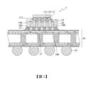
圖1係為習知半導體封裝件1之剖面示意圖。如圖1所示,該半導體封裝件1之製法係先提供一矽中介板(Through Silicon interposer,簡稱TSI)10,該矽中介板10具有具有相對之置晶側10a與轉接側10b及連通該置晶側10a與轉接側10b之複數導電矽穿孔(Through-silicon via,簡稱TSV)100,且該置晶側10a上具有一電性連接該些導電矽穿孔100之線路重佈層(Redistribution layer,簡稱RDL)12;接著,將一半導體晶片11以其電極墊110藉由複數銲錫凸塊111電性結合至該線路重佈層12上,並於該半導體晶片11與該矽中介板10之間填充底膠(underfill)112以包覆該些銲錫凸塊111;之後,將一封裝基板16以其銲墊160藉由複數如銲料凸塊或銅柱之C4規格導電元件15電性結合於該導電矽穿孔100上,並於該矽中介板10與該封裝基板16之間填充另一底膠17以包覆該些導電元件15;最後,於該封裝基板16底側接置複數銲球19以外接一電路板(圖略)。FIG. 1 is a cross-sectional view of a conventional semiconductor package 1. As shown in FIG. 1 , the manufacturing method of the semiconductor package 1 is to first provide a through silicon interposer (TSI) 10, wherein the silicon interposer 10 has a
惟,習知半導體封裝件1中,採用矽中介板10作為半導體晶片11與電路板之間訊號傳遞的介質,故於製作該矽中介板10時,需製作習知導電矽穿孔100及C4規格導電元件15等製程,因而大幅增加製程難度及製作成本,且該封裝基板16需透過該導電元件15傳導電性訊號及散熱,致使該封裝基板16之導電效能及散熱效能不佳。However, in the conventional semiconductor package 1, a silicon interposer 10 is used as a medium for signal transmission between the
再者,該矽中介板10需藉由該些導電元件15設於該封裝基板16上,致使該半導體封裝件1之整體厚度難以降低,導致應用該半導體封裝件1之電子產品難以符合微小化之需求。Furthermore, the silicon interposer 10 needs to be disposed on the
又,習知半導體封裝件1於製作過程中,該封裝基板16與該矽中介板10之間的熱膨脹係數(CTE)不匹配(mismatch),因而容易發生熱應力不均勻之情況,致使於後續回焊銲錫凸塊111、導電元件15與銲球19時,該封裝基板16會產生極大之翹曲(warpage),以致於發生植球狀況不佳(即該銲球19掉落)、銲球19不沾錫(non-wetting)或該封裝基板16裂開等可靠度問題,進而導致應用該半導體封裝件1之終端電子產品(如電腦、手機等)發生可靠度問題。In addition, it is known that during the manufacturing process of the semiconductor package 1, the coefficient of thermal expansion (CTE) between the
另外,矽材與金屬材之結合性不佳,因而不利於製作該線路重佈層12,使該線路重佈層12與該矽中介板10容易發生分離之風險。In addition, the bonding between silicon and metal is not good, which is not conducive to the production of the
因此,如何克服上述習知製法的種種問題,實已成目前亟欲解決的課題。Therefore, how to overcome the above-mentioned problems of the knowledge-based manufacturing method has become an issue that needs to be solved urgently.
鑑於上述習知技術之種種缺失,本發明係提供一種封裝基板,係包括:佈線結構,係具有相對之第一側與第二側,其中,該佈線結構係包含至少一絕緣層及設於該絕緣層上之佈線層,且形成該絕緣層之材質係為味之素增層膜(Ajinomoto build-up film);第一線路結構,係設於該佈線結構之第一側上,其中,該第一線路結構係包含至少一形成於該絕緣層上之第一介電層及設於該第一介電層上且電性連接該佈線層之第一線路層,且形成該第一介電層之材質不同於形成該絕緣層之材質;以及第二線路結構,係設於該佈線結構之第二側上,其中,該第二線路結構係包含至少一形成於該絕緣層上之第二介電層及設於該第二介電層上且電性連接該佈線層之第二線路層,且形成該第二介電層之材質不同於形成該絕緣層之材質。In view of the above-mentioned deficiencies of the prior art, the present invention provides a packaging substrate, comprising: a wiring structure having a first side and a second side opposite to each other, wherein the wiring structure comprises at least one insulating layer and a wiring layer disposed on the insulating layer, and the material forming the insulating layer is Ajinomoto build-up film. film); a first circuit structure is disposed on a first side of the wiring structure, wherein the first circuit structure includes at least one first dielectric layer formed on the insulating layer and a first circuit layer disposed on the first dielectric layer and electrically connected to the wiring layer, and the material forming the first dielectric layer is different from the material forming the insulating layer; and a second circuit structure is disposed on a second side of the wiring structure, wherein the second circuit structure includes at least one second dielectric layer formed on the insulating layer and a second circuit layer disposed on the second dielectric layer and electrically connected to the wiring layer, and the material forming the second dielectric layer is different from the material forming the insulating layer.
前述之封裝基板中,該第一線路結構係結合至一核心板體,該核心板體具有相對之第一表面及第二表面,以令該第一線路結構結合至該核心板體之第一表面上,且該核心板體係具有複數連通該第一與第二表面之導電通孔,以令該導電通孔電性連接該第一線路層。In the aforementioned package substrate, the first circuit structure is bonded to a core board, the core board has a first surface and a second surface opposite to each other, so that the first circuit structure is bonded to the first surface of the core board, and the core board has a plurality of conductive vias connecting the first and second surfaces, so that the conductive vias are electrically connected to the first circuit layer.
本發明亦提供一種電子封裝件,係包括:前述之封裝基板;以及電子元件,係設於該第二線路結構上且電性連接該第二線路層。The present invention also provides an electronic package, comprising: the aforementioned package substrate; and an electronic component, which is disposed on the second circuit structure and electrically connected to the second circuit layer.
本發明又提供一種封裝基板之製法,係包括:形成佈線結構於一承載件上,該佈線結構係具有相對之第一側與第二側,以令該佈線結構以其第二側結合該承載件,其中,該佈線結構係包含至少一絕緣層及設於該絕緣層上之佈線層,且形成該絕緣層之材質係為味之素增層膜(Ajinomoto build-up film);形成第一線路結構於該佈線結構之第一側上,其中,該第一線路結構係包含至少一形成於該絕緣層上之第一介電層及設於該第一介電層上且電性連接該佈線層之第一線路層,且形成該第一介電層之材質不同於形成該絕緣層之材質;移除該承載件,以外露出該佈線結構之第二側;以及形成第二線路結構於該佈線結構之第二側上,其中,該第二線路結構係包含至少一形成於該絕緣層上之第二介電層及設於該第二介電層上且電性連接該佈線層之第二線路層,且形成該第二介電層之材質不同於形成該絕緣層之材質。The present invention also provides a method for manufacturing a package substrate, comprising: forming a wiring structure on a carrier, the wiring structure having a first side and a second side opposite to each other, so that the wiring structure is combined with the carrier by its second side, wherein the wiring structure comprises at least one insulating layer and a wiring layer disposed on the insulating layer, and the material forming the insulating layer is Ajinomoto build-up film. film); forming a first circuit structure on a first side of the wiring structure, wherein the first circuit structure includes at least a first dielectric layer formed on the insulating layer and a first wiring layer disposed on the first dielectric layer and electrically connected to the wiring layer, and the material forming the first dielectric layer is different from the material forming the insulating layer; removing the carrier, and Exposing the second side of the wiring structure; and forming a second wiring structure on the second side of the wiring structure, wherein the second wiring structure includes at least a second dielectric layer formed on the insulating layer and a second wiring layer disposed on the second dielectric layer and electrically connected to the wiring layer, and the material forming the second dielectric layer is different from the material forming the insulating layer.
本發明復提供一種封裝基板之製法,係包括:提供一核心板體,其具有相對之第一表面及第二表面,且該核心板體係具有複數連通該第一與第二表面之導電通孔;形成第一線路結構於該核心板體之第一表面上,其中,該第一線路結構係包含至少一形成於該核心板體上之第一介電層及設於該第一介電層上且電性連接該導電通孔之第一線路層;形成佈線結構於該第一線路結構上,且該佈線結構係具有相對之第一側與第二側,以令該佈線結構以其第一側結合該第一線路結構,其中,該佈線結構係包含至少一形成於該第一介電層上之絕緣層及設於該絕緣層上之佈線層,且形成該絕緣層之材質係為味之素增層膜(Ajinomoto build-up film),其不同於形成該第一介電層之材質;以及形成第二線路結構於該佈線結構之第二側上,其中,該第二線路結構係包含至少一形成於該絕緣層上之第二介電層及設於該第二介電層上且電性連接該佈線層之第二線路層,且形成該第二介電層之材質不同於形成該絕緣層之材質。The present invention further provides a method for manufacturing a package substrate, comprising: providing a core board having a first surface and a second surface opposite to each other, and the core board having a plurality of conductive through holes connecting the first and second surfaces; forming a first circuit structure on the first surface of the core board, wherein the first circuit structure includes at least one first dielectric layer formed on the core board and a first dielectric layer disposed on the first dielectric layer and electrically connected to the first and second surfaces; A first wiring layer of a conductive through hole; forming a wiring structure on the first wiring structure, and the wiring structure has a first side and a second side opposite to each other, so that the wiring structure is combined with the first wiring structure with its first side, wherein the wiring structure includes at least one insulating layer formed on the first dielectric layer and a wiring layer disposed on the insulating layer, and the material forming the insulating layer is Ajinomoto build-up film (Ajinomoto A build-up film) is formed of a material different from that of the first dielectric layer; and a second wiring structure is formed on a second side of the wiring structure, wherein the second wiring structure includes at least a second dielectric layer formed on the insulating layer and a second wiring layer disposed on the second dielectric layer and electrically connected to the wiring layer, and the material forming the second dielectric layer is different from that forming the insulating layer.
前述之封裝基板及其兩種製法中,該第一與第二介電層之材質係相異。In the aforementioned packaging substrate and its two manufacturing methods, the materials of the first and second dielectric layers are different.
本發明另提供一種電子封裝件之製法,係包括:提供一前述之封裝基板;以及將電子元件設於該第二線路結構上,且該電子元件電性連接該第二線路層。The present invention also provides a method for manufacturing an electronic package, which includes: providing a package substrate as described above; and placing an electronic component on the second circuit structure, and the electronic component is electrically connected to the second circuit layer.
前述之電子封裝件及其製法,復包括形成外接元件於該第一線路結構上,且該外接元件電性連接該第一線路層。The aforementioned electronic package and its manufacturing method further include forming an external component on the first circuit structure, and the external component is electrically connected to the first circuit layer.
由上可知,本發明之電子封裝件及其封裝基板與製法,主要藉由ABF作為絕緣層以取代習知矽板體,並利用佈線層作為電子元件與電路板之間訊號傳遞的介質,故相較於習知技術,本發明無需製作習知矽中介板有關導電矽穿孔及C4規格導電元件等之製程,因而能大幅降低製程難度及製作成本,且該封裝基板之導電效能及散熱效能大幅提升。As can be seen from the above, the electronic package and its packaging substrate and manufacturing method of the present invention mainly use ABF as an insulating layer to replace the conventional silicon board, and use the wiring layer as a medium for signal transmission between electronic components and circuit boards. Therefore, compared with the conventional technology, the present invention does not need to manufacture the processes related to conductive silicon vias and C4 specification conductive components in the conventional silicon interposer, thereby greatly reducing the process difficulty and manufacturing cost, and the conductive performance and heat dissipation performance of the packaging substrate are greatly improved.
再者,本發明藉由該佈線結構直接接合該第一線路結構之設計,以取代習知矽中介板及C4規格導電元件之配合,使本發明之封裝基板之厚度有利於薄化需求。Furthermore, the present invention uses the design of directly connecting the wiring structure to the first circuit structure to replace the conventional silicon interposer and C4 specification conductive components, so that the thickness of the package substrate of the present invention is conducive to the thinning requirement.
又,藉由形成該絕緣層之材質不同於形成該第一與第二介電層之材質,以利於分散熱應力,使本發明之封裝基板於後續製程中可有效避免發生翹曲之問題。Furthermore, by forming the insulating layer with a material different from the material forming the first and second dielectric layers, thermal stress can be dispersed, so that the packaging substrate of the present invention can effectively avoid the problem of warping in subsequent manufacturing processes.
另外,本發明藉由ABF作為絕緣層之設計,以利於採用RDL製程製作該第二線路結構,使該第二線路層有利於符合高密度之細線路/細間距之需求,且能降低該第二線路結構與該佈線結構發生分離之風險。In addition, the present invention uses ABF as an insulating layer to facilitate the use of RDL process to manufacture the second circuit structure, so that the second circuit layer is conducive to meeting the requirements of high-density fine circuits/fine spacing, and can reduce the risk of separation between the second circuit structure and the wiring structure.
1:半導體封裝件1:Semiconductor packages
10:矽中介板10: Silicon interposer
10a:置晶側10a: Chip placement side
10b:轉接側10b: Adapter side
100:導電矽穿孔100: Conductive silicon vias
11:半導體晶片11: Semiconductor chip
110,400:電極墊110,400:Electrode pad
111:銲錫凸塊111:Solder bumps
112,17:底膠112,17: Base glue
12:線路重佈層12: Circuit redistribution layer
15:導電元件15: Conductive element
16,2a,3a:封裝基板16,2a,3a:Packaging substrate
160:銲墊160:Welding pad
19:銲球19: Shot
2,3:電子封裝件2,3: Electronic packaging
20,220,320:佈線層20,220,320: wiring layer
21,31a,31b:第一線路結構21,31a,31b: First line structure
210,310:第一線路層210,310: First circuit layer
211,311:第一介電層211,311: First dielectric layer
22,32:佈線結構22,32: Wiring structure
22a,32a:第一側22a,32a: First side
22b,32b:第二側22b,32b: Second side
221,321,322:絕緣層221,321,322: Insulation layer
23,33:第二線路結構23,33: Second circuit structure
230,330:第二線路層230,330: Second circuit layer
231,331:第二介電層231,331: Second dielectric layer
27,29:外接元件27,29: External components
30:核心板體30: Core board
30a:第一表面30a: First surface
30b:第二表面30b: Second surface
300:導電通孔300: Conductive vias
300a:塞孔材料300a: plugging material
301,302:內線路層301,302: Inner line layer
40,41,42,43:電子元件40,41,42,43: Electronic components
40a:作用面40a: Action surface
40b:非作用面40b: Non-active surface
44:導電凸塊44: Conductive bump
45:被動元件45: Passive components
9:承載件9: Carrier
90:板體90: Plate
91:金屬層91:Metal layer
圖1係為習知半導體封裝件之剖視圖。Figure 1 is a cross-sectional view of a conventional semiconductor package.
圖2A至圖2E係為本發明之電子封裝件之製法之第一實施例之剖面示意圖。Figures 2A to 2E are cross-sectional schematic diagrams of the first embodiment of the method for manufacturing the electronic package of the present invention.
圖3A至圖3D係為本發明之電子封裝件之製法之第二實施例之剖面示意圖。Figures 3A to 3D are cross-sectional schematic diagrams of the second embodiment of the method for manufacturing the electronic package of the present invention.
以下藉由特定的具體實施例說明本發明之實施方式,熟悉此技藝之人士可由本說明書所揭示之內容輕易地瞭解本發明之其他優點及功效。The following is a specific and concrete example to illustrate the implementation of the present invention. People familiar with this technology can easily understand other advantages and effects of the present invention from the content disclosed in this manual.
須知,本說明書所附圖式所繪示之結構、比例、大小等,均僅用以配合說明書所揭示之內容,以供熟悉此技藝之人士之瞭解與閱讀,並非用以限定本發明可實施之限定條件,故不具技術上之實質意義,任何結構之修飾、比例關係之改變或大小之調整,在不影響本發明所能產生之功效及所能達成之目的下,均應仍落在本發明所揭示之技術內容得能涵蓋之範圍內。同時,本說明書中所引用之如「上」、「第一」、「第二」、「一」等之用語,亦僅為便於敘述之明瞭,而非用以限定本發明可實施之範圍,其相對關係之改變或調整,在無實質變更技術內容下,當亦視為本發明可實施之範疇。It should be noted that the structures, proportions, sizes, etc. depicted in the drawings attached to this specification are only used to match the contents disclosed in the specification for understanding and reading by people familiar with this technology, and are not used to limit the conditions under which the present invention can be implemented. Therefore, they have no substantial technical significance. Any modification of the structure, change of the proportion relationship or adjustment of the size shall still fall within the scope of the technical content disclosed by the present invention without affecting the effect and purpose that can be achieved by the present invention. At the same time, the terms such as "above", "first", "second", "one" etc. used in this specification are only for the convenience of description and are not used to limit the scope of implementation of the present invention. Changes or adjustments in their relative relationships shall also be regarded as the scope of implementation of the present invention without substantially changing the technical content.
圖2A至圖2E係為本發明之電子封裝件2之製法之第一實施例的剖面示意圖。Figures 2A to 2E are cross-sectional schematic diagrams of the first embodiment of the method for manufacturing the
如圖2A所示,於一承載件9上形成一佈線層20。As shown in FIG. 2A , a
於本實施例中,該承載件9係為暫時性載板,如銅箔基板或其它板材。例如,該承載件9為銅箔基板,其板體90之相對兩側具有金屬層91。In this embodiment, the
再者,該佈線層20藉由該金屬層91以電鍍金屬(如銅材)或其它方式製作成圖案化線路。Furthermore, the
如圖2B所示,以對稱方式形成一佈線結構22分別於該承載件9之相對兩側上,再於該佈線結構22上形成一第一線路結構21。As shown in FIG. 2B , a
於本實施例中,各該佈線結構22係定義有相對之第一側22a及第二側22b,且該佈線結構22以其第二側22b結合該承載件9,並於該佈線結構22之第一側22a上形成該第一線路結構21。In this embodiment, each
再者,該佈線結構22係包含至少一覆蓋該佈線層20之絕緣層221、及形成於該絕緣層221上之另一佈線層220,使該另一佈線層220電性連接該金屬層91上之佈線層20,即該另一佈線層220採用形成於該絕緣層221上之雷射盲孔內所電鍍之導電體電性導通該金屬層91上之佈線層20。例如,形成該絕緣層221之材質係為味之素增層膜(Ajinomoto build-up film,簡稱ABF),其熱膨脹係數(Coefficient of thermal expansion,簡稱CTE)為13至17ppm/℃,且該佈線層220以電鍍金屬(如銅材)或其它方式製作成圖案化線路。應可理解地,利用增層(build-up process)法,該些佈線結構22可依需求增設多層絕緣層221,以製作多層佈線層220。Furthermore, the
又,該第一線路結構21係包含至少一形成於該絕緣層221上之第一介電層211、及形成於該第一介電層211上之第一線路層210,以令該第一線路層210電性連接該佈線層220,即該第一線路層210採用形成於該第一介電層211上之雷射盲孔內所電鍍之導電體電性導通該佈線層220。例如,採用增層法製作該第一線路結構21,使該第一線路結構21可依需求增設多層第一介電層211,以製作多層第一線路層210,且形成該第一介電層211之材質係如聚對二唑苯(Polybenzoxazole,簡稱PBO)、聚醯亞胺(Polyimide,簡稱PI)、具玻纖之預浸材(Prepreg,簡稱PP)或其它等介電材。因此,形成該第一介電層211之材質與形成該絕緣層221之材質可不相同,例如,形成該第一介電層211之材質係為預浸材(PP),其熱膨脹係數(CTE)為10ppm/℃。Furthermore, the
另外,該第一線路層210之線寬/線距約至多為50/50微米(um),且該佈線層220之線寬/線距約至多為10/10微米(um)。In addition, the line width/line spacing of the
如圖2C所示,移除該承載件9,以外露出該佈線結構22之第二側22b及其內之佈線層20。As shown in FIG. 2C , the
於本實施例中,可先剝離或研磨該板體90,再蝕刻移除該金屬層91,使該佈線層20齊平或略凹於該佈線結構22之第二側22b之表面。In this embodiment, the
如圖2D所示,於該佈線結構22之第二側22b上形成一第二線路結構23,以形成封裝基板2a,其佈線層20係電性連接該第二線路結構23。As shown in FIG. 2D , a
於本實施例中,可於該佈線結構22之第二側22b上採用增層法形成該第二線路結構23,使該第二線路結構23可依需求增設多層第二介電層231,以製作多層第二線路層230。例如,該第二線路結構23係包含至少一形成於該絕緣層221上之第二介電層231、及形成於該第二介電層231上之第二線路層230,以令該第二線路層230電性連接該佈線層20。In this embodiment, the
再者,該第二線路層230係為線路重佈層(redistribution layer,簡稱RDL)規格,其線寬/線距約為2/2至5/5um微米(um),且形成該第二介電層231之材質係如聚對二唑苯(PBO)、聚醯亞胺(PI)、具玻纖之預浸材(PP)或其它等介電材。例如,形成該第二介電層231之材質係為聚醯亞胺(PI),其CTE為30~35ppm/℃,使該第二介電層231之材質不同於該第一介電層211及該絕緣層221之材質。Furthermore, the
如圖2E所示,將至少一電子元件40,41,42,43設於該第二線路結構23上,使該電子元件40,41,42,43電性連接該第二線路層230。此外,亦可形成包覆該電子元件40,41,42,43之封裝膠體(圖略)。As shown in FIG. 2E , at least one
於本實施例中,該電子元件40係為主動元件、被動元件或其二者組合,其中,該主動元件係例如半導體晶片,且該被動元件係例如電阻、電容或電感。例如,若該電子元件40為半導體晶片,其具有相對之作用面40a與非作用面40b,該作用面40a係具有複數電極墊400,其以作用面40a朝下方式(如覆晶方式)透過複數導電凸塊44電性連接該第二線路層230;或者,該電子元件40亦可藉由複數銲線(圖略)以打線方式電性連接該第二線路層230;亦或,該電子元件40可直接接觸該第二線路層230。然而,有關該電子元件40電性連接第二線路層230之方式不限於上述。In this embodiment, the
再者,該電子元件41,42,43亦可為不相同類型的電子元件。例如,將一如控制晶片之電子元件41透過複數導電凸塊44設於該封裝基板2a上,其上堆疊至少一高頻寬記憶體(High Bandwidth Memory,簡稱HBM)型晶片之電子元件42,43,且該電子元件41電性連接該第二線路層230。Furthermore, the
又,該封裝基板2a之相對兩側之用途不同。例如,該第二線路結構23係作為用以接置半導體晶片之置晶側,且該第一線路結構21係作為用以接置電路板之植球側,故該第一線路結構21之最外側之第一線路層210可結合複數如焊球之外接元件27,以外接如電路板之電子裝置(圖略)。Furthermore, the two opposite sides of the
另外,該封裝基板2a之植球側亦可依需求配置電子元件,如被動元件45。In addition, the ball implantation side of the
因此,本發明之製法係以ABF之絕緣層221取代習知矽板體,並利用佈線層20,220作為電子元件40,41,42,43與電路板之間訊號傳遞的介質,故無需製作習知矽中介板有關導電矽穿孔及C4規格導電元件等之製程,因而大幅降低製程難度及製作成本。Therefore, the manufacturing method of the present invention replaces the conventional silicon board with the
進一步,藉由該第一線路層210與該佈線層220直接相互接觸連接(即採用雷射盲孔內所電鍍之導電體電性導通),以取代習知C4規格導電元件之傳導,故相較於習知封裝基板,該封裝基板2a之導電效能及散熱效能大幅提升。Furthermore, by directly connecting the
再者,藉由該佈線層20嵌埋於該絕緣層221中,且該第一線路結構21與該佈線結構22等之無核心式設計,以取代習知矽中介板,使該封裝基板2a之厚度有利於薄化需求。Furthermore, by embedding the
又,該封裝基板2a之各層介電層之排設方式係依據CTE大小漸增或漸減,以避免該封裝基板2a發生翹曲之問題。例如,基於該封裝基板2a由其植球側朝置晶側之方向(如圖2E所示之由下往上之方向),該第一介電層211之CTE最小,該第二介電層231之CTE最大,故於後續進行如回焊外接元件27或回焊導電凸塊44等之熱製程時,能有效防止該封裝基板發生翹曲,以避免該外接元件27(或導電凸塊44)脫落(peeled)、碎裂(crack)、偏位(shift)或其它影響良率之狀況等。In addition, the arrangement of each dielectric layer of the
另外,藉由ABF作為絕緣層221及該佈線層20嵌埋於該絕緣層221中之設計,以利於採用RDL製程製作該第二線路層230,使該第二線路層230利於符合高密度之細線路/細間距之需求,且能降低該第二線路層230與該佈線結構22發生分離(peeled)之風險。In addition, by using ABF as the insulating
圖3A至圖3D係為本發明之電子封裝件3之製法之第二實施例之剖面示意圖。本實施例與第一實施例之差異在於該封裝基板3a之形式,故以下不再贅述相同處。Figures 3A to 3D are cross-sectional schematic diagrams of the second embodiment of the method for manufacturing the
如圖3A所示,提供一核心板體30,其具有相對之第一表面30a及第二表面30b,並於該核心板體30之第一表面30a及第二表面30b上佈設有內線路層301,302,且該核心板體30係具有複數連通該第一表面30a與第二表面30b之導電通孔300,以令該導電通孔300電性連接該些內線路層301,302。As shown in FIG. 3A , a
於本實施例中,該核心板體30可為包含雙順丁烯二酸醯亞胺/三氮阱(Bismaleimide triazine,簡稱BT)、具玻纖之預浸材(Prepreg,簡稱PP)之有機聚合板材或其它板材,且該導電通孔300中係為中空柱狀,其可於中空處填滿塞孔材料300a,其中,該塞孔材料300a之種類繁多,如導電膠、油墨等,並無特別限制。應可理解地,於其他實施例中,該導電通孔300亦可為實心金屬柱體,而無需填入塞孔材料300a。In this embodiment, the
再者,於該核心板體30之第一表面30a與第二表面30b上分別形成第一線路結構31a,31b,該第一線路結構31a,31b係包含至少一形成於該核心板體30上之第一介電層311、及形成於該第一介電層311上之第一線路層310,以令該第一線路層310電性連接該內線路層301,302。例如,採用增層法製作該第一線路結構31a,31b,且該第一介電層311係如聚對二唑苯(Polybenzoxazole,簡稱PBO)、聚醯亞胺(Polyimide,簡稱PI)、具玻纖之預浸材(Prepreg,簡稱PP)或其它等介電材。Furthermore,
如圖3B所示,進行圖案化製程,以於該核心板體30之其中一表面(如第一表面30a)上之第一線路結構31a上形成佈線結構32。As shown in FIG. 3B , a patterning process is performed to form a
於本實施例中,各該佈線結構32係定義有相對之第一側32a及第二側32b,且該佈線結構32以其第一側32a結合該第一線路結構31a。In this embodiment, each
再者,該佈線結構32係包含至少一絕緣層321、及形成於該絕緣層321上之佈線層320,使該佈線層320電性連接該第一線路層310。例如,形成該絕緣層321之材質係為味之素增層膜(Ajinomoto build-up film,簡稱ABF),且該佈線層320以電鍍金屬(如銅材)或其它方式製作成圖案化線路。應可理解地,利用增層(build-up process)法,該些佈線結構32可依需求增設多層該絕緣層321,以製作多層佈線層320。Furthermore, the
又,該佈線結構32係於最外側之佈線層320上形成另一絕緣層322,以令該佈線層320齊平該絕緣層322,使該佈線層320外露於該絕緣層322。Furthermore, the
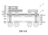
如圖3C所示,於該佈線結構32之第二側32b上形成一第二線路結構33,以形成一不對稱式封裝基板3a,其佈線層320係電性連接該第二線路結構33。As shown in FIG. 3C , a second circuit structure 33 is formed on the
於本實施例中,可於該佈線結構32之第二側32b上採用增層法形成該第二線路結構33。例如,該第二線路結構33係包含至少一形成於該絕緣層321上之第二介電層331、及形成於該第二介電層331上之第二線路層330,以令該第二線路層330電性連接該佈線層320。In this embodiment, the second circuit structure 33 can be formed on the
再者,該第二線路層330係為線路重佈層(redistribution layer,簡稱RDL)規格,且形成該第二介電層331之材質係如聚對二唑苯(Polybenzoxazole,簡稱PBO)、聚醯亞胺(Polyimide,簡稱PI)、具玻纖之預浸材(Prepreg,簡稱PP)或其它等介電材。例如,形成該第二介電層331之材質係為聚醯亞胺(PI),使該第二介電層331之材質不同於該第一介電層311及該絕緣層321之材質。Furthermore, the second circuit layer 330 is a circuit redistribution layer (RDL) specification, and the material forming the
如圖3D所示,將至少一電子元件40,41,42,43設於該第二線路結構33上,使該電子元件40,41,42,43電性連接該第二線路層330。此外,亦可形成包覆該電子元件40,41,42,43之封裝膠體(圖略)。As shown in FIG. 3D , at least one
於本實施例中,該封裝基板3a之相對兩側之用途不同。例如,該第二線路結構33係作為用以接置半導體晶片之置晶側,且該第一線路結構31b係作為用以接置電路板之植球側,故該第一線路結構31b之最外側之第一線路層310可結合複數如焊球之外接元件29,以外接如電路板之電子裝置(圖略)。In this embodiment, the two opposite sides of the package substrate 3a have different uses. For example, the second circuit structure 33 is used as a chip placement side for mounting a semiconductor chip, and the
因此,本發明之製法係以ABF之絕緣層321取代習知矽板體,並利用佈線層320作為電子元件40,41,42,43與電路板之間訊號傳遞的介質,故無需製作習知矽中介板有關導電矽穿孔及C4規格導電元件等之製程,因而大幅降低製程難度及製作成本。Therefore, the manufacturing method of the present invention replaces the conventional silicon board with the
進一步,藉由該第一線路層310與該佈線層320直接相互接觸連接(即採用雷射盲孔內所電鍍之導電體電性導通),以取代習知C4規格導電元件之傳導,故相較於習知封裝基板,該封裝基板3a之導電效能及散熱效能大幅提升。Furthermore, by directly connecting the
再者,藉由該佈線結構32直接結合該第一線路結構31a,因而免用習知C4規格導電元件,故該封裝基板2a之厚度有利於薄化需求。Furthermore, by directly combining the
又,該封裝基板3a之各層介電層之排設方式係依據CTE大小漸增或漸減,可避免該封裝基板3a發生翹曲之問題。In addition, the arrangement of the dielectric layers of the package substrate 3a is based on the gradual increase or decrease of the CTE size, which can avoid the problem of warping of the package substrate 3a.
另外,藉由ABF作為絕緣層321之設計,以利於採用RDL製程製作該第二線路層330,使該第二線路層330有利於符合高密度之細線路/細間距之需求。In addition, by using ABF as the insulating
本發明亦提供一種封裝基板2a,3a,係包括:一佈線結構22,32、一第一線路結構21,31a、以及第二線路結構23,33。The present invention also provides a
所述之佈線結構22,32係具有相對之第一側22a,32a與第二側22b,32b,其中,該佈線結構22,32係包含至少一絕緣層221,321,322及設於該絕緣層221,321,322上之佈線層220,320,且形成該絕緣層221,321,322之材質係為味之素增層膜(Ajinomoto build-up film)。The
所述之第一線路結構21,31a係設於該佈線結構22,32之第一側22a,32a上,其中,該第一線路結構21,31a係包含至少一形成於該絕緣層221,321上之第一介電層211,311及設於該第一介電層211,311上且電性連接該佈線層220,320之第一線路層210,310,且形成該第一介電層211,311之材質不同於形成該絕緣層221,321,322之材質。The
所述之第二線路結構23,33係設於該佈線結構22,32之第二側22b,32b上,其中,該第二線路結構23,33係包含至少一形成於該絕緣層221,322上之第二介電層231,331及設於該第二介電層231,331上且電性連接該佈線層220,320之第二線路層230,330,且形成該第二介電層231,331之材質不同於形成該絕緣層221,321,322之材質。The
於一實施例中,該第一介電層211,311與第二介電層231,331之材質係相異。In one embodiment, the materials of the
於一實施例中,該第一線路結構31a係結合至一核心板體30,該核心板體30具有相對之第一表面30a及第二表面30b,以令該第一線路結構31a結合至該核心板體30之第一表面30a上,且該核心板體30係具有複數連通該第一與第二表面30a,30b之導電通孔300,以令該導電通孔300電性連接該第一線路層310。In one embodiment, the
本發明亦提供一種電子封裝件2,3,係包括:前述之封裝基板2a,3a、以及設於該第二線路結構23,33上且電性連接該第二線路層230,330之電子元件40,41,42,43。The present invention also provides an
於一實施例中,所述之電子封裝件2,3復包括形成於該第一線路結構21,31b上且電性連接該第一線路層210,310之外接元件27。In one embodiment, the
綜上所述,本發明之電子封裝件及其封裝基板與製法,係藉由ABF作為絕緣層以取代習知矽板體,並利用佈線層作為電子元件與電路板之間訊號傳遞的介質,故本發明無需製作習知矽中介板有關導電矽穿孔及C4規格導電元件等之製程,因而能大幅降低製程難度及製作成本,且該封裝基板之導電效能及散熱效能大幅提升。In summary, the electronic package and its packaging substrate and manufacturing method of the present invention use ABF as an insulating layer to replace the conventional silicon board, and use the wiring layer as a medium for signal transmission between the electronic components and the circuit board. Therefore, the present invention does not need to manufacture the processes related to conductive silicon vias and C4 specification conductive components in the conventional silicon interposer, thereby greatly reducing the process difficulty and manufacturing cost, and the conductive performance and heat dissipation performance of the packaging substrate are greatly improved.
再者,藉由該佈線結構直接接合該第一線路結構之設計,以取代習知矽中介板及C4規格導電元件之配合,使該封裝基板之厚度有利於薄化需求。Furthermore, by directly connecting the wiring structure to the first circuit structure, the conventional silicon interposer and C4 specification conductive components are replaced, so that the thickness of the package substrate is conducive to the thinning requirement.
又,該封裝基板之各層介電層之排設方式係依據CTE大小漸增或漸減,以避免該封裝基板於後續製程中發生翹曲之問題。In addition, the arrangement of the dielectric layers of the package substrate is gradually increased or decreased according to the CTE size to avoid the problem of warping of the package substrate in subsequent manufacturing processes.
另外,藉由ABF作為絕緣層之設計,以利於採用RDL製程製作該第二線路結構,使該第二線路層有利於符合高密度之細線路/細間距之需求,且能降低該第二線路結構與該佈線結構發生分離之風險。In addition, by using ABF as the insulating layer, it is convenient to use the RDL process to manufacture the second circuit structure, so that the second circuit layer can meet the requirements of high-density fine circuits/fine spacing, and can reduce the risk of separation between the second circuit structure and the wiring structure.
上述實施例係用以例示性說明本發明之原理及其功效,而非用於限制本發明。任何熟習此項技藝之人士均可在不違背本發明之精神及範疇下,對上述實施例進行修改。因此本發明之權利保護範圍,應如後述之申請專利範圍所列。The above embodiments are used to illustrate the principles and effects of the present invention, but are not used to limit the present invention. Anyone familiar with this technology can modify the above embodiments without violating the spirit and scope of the present invention. Therefore, the scope of protection of the present invention should be as listed in the scope of the patent application described below.
2:電子封裝件2: Electronic packaging components
2a:封裝基板2a:Packaging substrate
21:第一線路結構21: First circuit structure
210:第一線路層210: First circuit layer
211:第一介電層211: First dielectric layer
22:佈線結構22: Wiring structure
221:絕緣層221: Insulation layer
23:第二線路結構23: Second circuit structure
230:第二線路層230: Second circuit layer
231:第二介電層231: Second dielectric layer
27:外接元件27: External components
40,41,42,43:電子元件40,41,42,43: Electronic components
40a:作用面40a: Action surface
40b:非作用面40b: Non-active surface
44:導電凸塊44: Conductive bump
45:被動元件45: Passive components
Claims (10)
Translated fromChinesePriority Applications (3)
| Application Number | Priority Date | Filing Date | Title |
|---|---|---|---|
| TW112102059ATWI850976B (en) | 2023-01-17 | 2023-01-17 | Electronic package, package substrate and fabricating method thereof |
| CN202310122119.5ACN118398590B (en) | 2023-01-17 | 2023-02-15 | Electronic package and package substrate and manufacturing method thereof |
| US18/414,740US20240243048A1 (en) | 2023-01-17 | 2024-01-17 | Electronic package, package substrate and manufacturing method thereof |
Applications Claiming Priority (1)
| Application Number | Priority Date | Filing Date | Title |
|---|---|---|---|
| TW112102059ATWI850976B (en) | 2023-01-17 | 2023-01-17 | Electronic package, package substrate and fabricating method thereof |
Publications (2)
| Publication Number | Publication Date |
|---|---|
| TW202431555A TW202431555A (en) | 2024-08-01 |
| TWI850976Btrue TWI850976B (en) | 2024-08-01 |
Family
ID=91853920
Family Applications (1)
| Application Number | Title | Priority Date | Filing Date |
|---|---|---|---|
| TW112102059ATWI850976B (en) | 2023-01-17 | 2023-01-17 | Electronic package, package substrate and fabricating method thereof |
Country Status (3)
| Country | Link |
|---|---|
| US (1) | US20240243048A1 (en) |
| CN (1) | CN118398590B (en) |
| TW (1) | TWI850976B (en) |
Families Citing this family (1)
| Publication number | Priority date | Publication date | Assignee | Title |
|---|---|---|---|---|
| US20240304555A1 (en)* | 2023-03-08 | 2024-09-12 | Advanced Semiconductor Engineering, Inc. | Package structure and method for manufacturing the same |
Citations (3)
| Publication number | Priority date | Publication date | Assignee | Title |
|---|---|---|---|---|
| TW201701419A (en)* | 2015-06-29 | 2017-01-01 | 矽品精密工業股份有限公司 | Package structure and the manufacture thereof |
| TW202202033A (en)* | 2020-06-24 | 2022-01-01 | 欣興電子股份有限公司 | Substrate structure with heat dissipation structure and manufacturing method thereof |
| TWI781049B (en)* | 2022-01-24 | 2022-10-11 | 欣興電子股份有限公司 | Circuit board structure and manufacturing method thereof |
Family Cites Families (6)
| Publication number | Priority date | Publication date | Assignee | Title |
|---|---|---|---|---|
| TW200839999A (en)* | 2007-03-30 | 2008-10-01 | Phoenix Prec Technology Corp | Packaging substrate structure |
| CN102054710B (en)* | 2009-11-06 | 2013-01-16 | 欣兴电子股份有限公司 | Manufacturing method of coreless layer encapsulation substrate |
| TWI550814B (en)* | 2015-07-31 | 2016-09-21 | 矽品精密工業股份有限公司 | Carrier body, package substrate, electronic package and method of manufacture thereof |
| TWI738069B (en)* | 2019-09-27 | 2021-09-01 | 恆勁科技股份有限公司 | Flip-chip package substrate and preparation method thereof |
| US11342272B2 (en)* | 2020-06-11 | 2022-05-24 | Advanced Semiconductor Engineering, Inc. | Substrate structures, and methods for forming the same and semiconductor package structures |
| KR20220141643A (en)* | 2021-04-13 | 2022-10-20 | 엘지이노텍 주식회사 | Circuit board and package substrate having the same |
- 2023
- 2023-01-17TWTW112102059Apatent/TWI850976B/enactive
- 2023-02-15CNCN202310122119.5Apatent/CN118398590B/enactiveActive
- 2024
- 2024-01-17USUS18/414,740patent/US20240243048A1/enactivePending
Patent Citations (3)
| Publication number | Priority date | Publication date | Assignee | Title |
|---|---|---|---|---|
| TW201701419A (en)* | 2015-06-29 | 2017-01-01 | 矽品精密工業股份有限公司 | Package structure and the manufacture thereof |
| TW202202033A (en)* | 2020-06-24 | 2022-01-01 | 欣興電子股份有限公司 | Substrate structure with heat dissipation structure and manufacturing method thereof |
| TWI781049B (en)* | 2022-01-24 | 2022-10-11 | 欣興電子股份有限公司 | Circuit board structure and manufacturing method thereof |
Also Published As
| Publication number | Publication date |
|---|---|
| CN118398590B (en) | 2025-06-06 |
| TW202431555A (en) | 2024-08-01 |
| CN118398590A (en) | 2024-07-26 |
| US20240243048A1 (en) | 2024-07-18 |
Similar Documents
| Publication | Publication Date | Title |
|---|---|---|
| TWI698966B (en) | Electronic package and manufacturing method thereof | |
| CN103094244B (en) | Packaging substrate with embedded through-hole interposer and method for fabricating the same | |
| CN102543927B (en) | Packaging substrate with embedded through-hole interposer and manufacturing method thereof | |
| US10573615B2 (en) | Semiconductor package and method for fabricating base for semiconductor package | |
| KR101333801B1 (en) | Flip chip substrate package assembly and process for making same | |
| TWI544599B (en) | Fabrication method of package structure | |
| CN116895636B (en) | Package substrate and method for fabricating the same | |
| TW202318587A (en) | Electronic package and manufacturing method thereof | |
| TW202343717A (en) | Electronic package | |
| CN118553709B (en) | Packaging substrate and manufacturing method thereof | |
| US12412869B2 (en) | Electronic structure having first and second thermal conductive materials covering conductive bumps and manufacturing method thereof, and electronic package having electronic structure and manufacturing method thereof | |
| US20230136788A1 (en) | Semiconductor substrate structure and manufacturing method thereof | |
| US20240243048A1 (en) | Electronic package, package substrate and manufacturing method thereof | |
| US20250029911A1 (en) | Manufacturing method of semiconductor substrate | |
| CN111755409A (en) | Semiconductor packaging substrate and its manufacturing method and electronic package and its manufacturing method | |
| TW202401684A (en) | Electronic package and manufacturing method thereof | |
| TWI762777B (en) | Semiconductor package substrate and manufacturing method thereof and electronic package and manufacturing method thereof | |
| TWI835561B (en) | Electronic package, package substrate and fabricating method thereof | |
| TWI804411B (en) | Electronic package and manufacturing method thereof | |
| US12148726B2 (en) | Semiconductor substrate structure, semiconductor structure and manufacturing method thereof | |
| CN220526907U (en) | Package structure | |
| US20250087572A1 (en) | Electronic package and fabricating method thereof | |
| TW202303900A (en) | Semiconductor package and its manufacturing method | |
| TW202414700A (en) | Electronic package and manufacturing method thereof | |
| TW202435374A (en) | Electronic package, carrier substrate and fabricating method thereof |