TWI849738B - Sensing device and manufacturing method thereof - Google Patents
Sensing device and manufacturing method thereofDownload PDFInfo
- Publication number
- TWI849738B TWI849738BTW112104897ATW112104897ATWI849738BTW I849738 BTWI849738 BTW I849738BTW 112104897 ATW112104897 ATW 112104897ATW 112104897 ATW112104897 ATW 112104897ATW I849738 BTWI849738 BTW I849738B
- Authority
- TW
- Taiwan
- Prior art keywords
- sensing
- layer
- sensing layer
- electrode
- present disclosure
- Prior art date
Links
- 238000004519manufacturing processMethods0.000titleclaimsabstractdescription31
- 239000000758substrateSubstances0.000claimsabstractdescription38
- 239000000463materialSubstances0.000claimsabstractdescription34
- 238000000034methodMethods0.000claimsdescription68
- 239000002245particleSubstances0.000claimsdescription66
- 239000000203mixtureSubstances0.000claimsdescription47
- 230000008569processEffects0.000claimsdescription43
- 239000011540sensing materialSubstances0.000claimsdescription43
- 238000010438heat treatmentMethods0.000claimsdescription26
- 238000000137annealingMethods0.000claimsdescription10
- 239000010410layerSubstances0.000description332
- 239000007789gasSubstances0.000description31
- 238000005979thermal decomposition reactionMethods0.000description12
- 230000015572biosynthetic processEffects0.000description10
- LFQSCWFLJHTTHZ-UHFFFAOYSA-NEthanolChemical compoundCCOLFQSCWFLJHTTHZ-UHFFFAOYSA-N0.000description6
- KFZMGEQAYNKOFK-UHFFFAOYSA-NIsopropanolChemical compoundCC(C)OKFZMGEQAYNKOFK-UHFFFAOYSA-N0.000description6
- XLOMVQKBTHCTTD-UHFFFAOYSA-NZinc monoxideChemical compound[Zn]=OXLOMVQKBTHCTTD-UHFFFAOYSA-N0.000description5
- 238000005229chemical vapour depositionMethods0.000description5
- XOLBLPGZBRYERU-UHFFFAOYSA-Ntin dioxideChemical compoundO=[Sn]=OXOLBLPGZBRYERU-UHFFFAOYSA-N0.000description5
- CSCPPACGZOOCGX-UHFFFAOYSA-NAcetoneChemical compoundCC(C)=OCSCPPACGZOOCGX-UHFFFAOYSA-N0.000description4
- 229910000480nickel oxideInorganic materials0.000description4
- 239000003575carbonaceous materialSubstances0.000description3
- 238000005137deposition processMethods0.000description3
- 229910044991metal oxideInorganic materials0.000description3
- 150000004706metal oxidesChemical class0.000description3
- 229910000476molybdenum oxideInorganic materials0.000description3
- PQQKPALAQIIWST-UHFFFAOYSA-NoxomolybdenumChemical compound[Mo]=OPQQKPALAQIIWST-UHFFFAOYSA-N0.000description3
- GNRSAWUEBMWBQH-UHFFFAOYSA-NoxonickelChemical compound[Ni]=OGNRSAWUEBMWBQH-UHFFFAOYSA-N0.000description3
- BASFCYQUMIYNBI-UHFFFAOYSA-NplatinumChemical compound[Pt]BASFCYQUMIYNBI-UHFFFAOYSA-N0.000description3
- 2380000101463D printingMethods0.000description2
- QGZKDVFQNNGYKY-UHFFFAOYSA-NAmmoniaChemical compoundNQGZKDVFQNNGYKY-UHFFFAOYSA-N0.000description2
- UQSXHKLRYXJYBZ-UHFFFAOYSA-NIron oxideChemical compound[Fe]=OUQSXHKLRYXJYBZ-UHFFFAOYSA-N0.000description2
- 239000004793PolystyreneSubstances0.000description2
- 238000000231atomic layer depositionMethods0.000description2
- 239000006229carbon blackSubstances0.000description2
- 238000000576coating methodMethods0.000description2
- 238000002485combustion reactionMethods0.000description2
- 239000004020conductorSubstances0.000description2
- 239000010949copperSubstances0.000description2
- SWXVUIWOUIDPGS-UHFFFAOYSA-Ndiacetone alcoholNatural productsCC(=O)CC(C)(C)OSWXVUIWOUIDPGS-UHFFFAOYSA-N0.000description2
- 239000010931goldSubstances0.000description2
- 238000004518low pressure chemical vapour depositionMethods0.000description2
- 229910052751metalInorganic materials0.000description2
- 239000002184metalSubstances0.000description2
- 230000035699permeabilityEffects0.000description2
- 238000000623plasma-assisted chemical vapour depositionMethods0.000description2
- 238000001289rapid thermal chemical vapour depositionMethods0.000description2
- 230000004044responseEffects0.000description2
- 239000004065semiconductorSubstances0.000description2
- 230000035945sensitivityEffects0.000description2
- 239000007784solid electrolyteSubstances0.000description2
- 238000006467substitution reactionMethods0.000description2
- 238000007669thermal treatmentMethods0.000description2
- XLYOFNOQVPJJNP-UHFFFAOYSA-NwaterChemical compoundOXLYOFNOQVPJJNP-UHFFFAOYSA-N0.000description2
- 229910001233yttria-stabilized zirconiaInorganic materials0.000description2
- 239000011787zinc oxideSubstances0.000description2
- PIGFYZPCRLYGLF-UHFFFAOYSA-NAluminum nitrideChemical compound[Al]#NPIGFYZPCRLYGLF-UHFFFAOYSA-N0.000description1
- OKTJSMMVPCPJKN-UHFFFAOYSA-NCarbonChemical compound[C]OKTJSMMVPCPJKN-UHFFFAOYSA-N0.000description1
- RYGMFSIKBFXOCR-UHFFFAOYSA-NCopperChemical compound[Cu]RYGMFSIKBFXOCR-UHFFFAOYSA-N0.000description1
- QPLDLSVMHZLSFG-UHFFFAOYSA-NCopper oxideChemical compound[Cu]=OQPLDLSVMHZLSFG-UHFFFAOYSA-N0.000description1
- 239000004593EpoxySubstances0.000description1
- 108091081062Repeated sequence (DNA)Proteins0.000description1
- 229910052581Si3N4Inorganic materials0.000description1
- VYPSYNLAJGMNEJ-UHFFFAOYSA-NSilicium dioxideChemical compoundO=[Si]=OVYPSYNLAJGMNEJ-UHFFFAOYSA-N0.000description1
- XUIMIQQOPSSXEZ-UHFFFAOYSA-NSiliconChemical compound[Si]XUIMIQQOPSSXEZ-UHFFFAOYSA-N0.000description1
- BQCADISMDOOEFD-UHFFFAOYSA-NSilverChemical compound[Ag]BQCADISMDOOEFD-UHFFFAOYSA-N0.000description1
- 229910006404SnO 2Inorganic materials0.000description1
- GWEVSGVZZGPLCZ-UHFFFAOYSA-NTitan oxideChemical compoundO=[Ti]=OGWEVSGVZZGPLCZ-UHFFFAOYSA-N0.000description1
- 229910052782aluminiumInorganic materials0.000description1
- XAGFODPZIPBFFR-UHFFFAOYSA-NaluminiumChemical compound[Al]XAGFODPZIPBFFR-UHFFFAOYSA-N0.000description1
- 229910021529ammoniaInorganic materials0.000description1
- 229910052802copperInorganic materials0.000description1
- 238000010586diagramMethods0.000description1
- 239000003989dielectric materialSubstances0.000description1
- 238000005516engineering processMethods0.000description1
- 239000011152fibreglassSubstances0.000description1
- PCHJSUWPFVWCPO-UHFFFAOYSA-NgoldChemical compound[Au]PCHJSUWPFVWCPO-UHFFFAOYSA-N0.000description1
- 229910052737goldInorganic materials0.000description1
- 229910021389grapheneInorganic materials0.000description1
- 230000003116impacting effectEffects0.000description1
- 238000009434installationMethods0.000description1
- 239000011810insulating materialSubstances0.000description1
- XEEYBQQBJWHFJM-UHFFFAOYSA-NironSubstances[Fe]XEEYBQQBJWHFJM-UHFFFAOYSA-N0.000description1
- 230000001788irregularEffects0.000description1
- 229910001092metal group alloyInorganic materials0.000description1
- 238000002156mixingMethods0.000description1
- 239000002102nanobeadSubstances0.000description1
- 239000002105nanoparticleSubstances0.000description1
- 150000004767nitridesChemical class0.000description1
- QGLKJKCYBOYXKC-UHFFFAOYSA-NnonaoxidotritungstenChemical compoundO=[W]1(=O)O[W](=O)(=O)O[W](=O)(=O)O1QGLKJKCYBOYXKC-UHFFFAOYSA-N0.000description1
- 229910052697platinumInorganic materials0.000description1
- 239000002861polymer materialSubstances0.000description1
- 229920002223polystyrenePolymers0.000description1
- 239000011241protective layerSubstances0.000description1
- 238000011084recoveryMethods0.000description1
- 229910052710siliconInorganic materials0.000description1
- 239000010703siliconSubstances0.000description1
- HBMJWWWQQXIZIP-UHFFFAOYSA-Nsilicon carbideChemical compound[Si+]#[C-]HBMJWWWQQXIZIP-UHFFFAOYSA-N0.000description1
- HQVNEWCFYHHQES-UHFFFAOYSA-Nsilicon nitrideChemical compoundN12[Si]34N5[Si]62N3[Si]51N64HQVNEWCFYHHQES-UHFFFAOYSA-N0.000description1
- -1silicon nitrideChemical class0.000description1
- 229910052814silicon oxideInorganic materials0.000description1
- 229910052709silverInorganic materials0.000description1
- 239000004332silverSubstances0.000description1
- 229910001887tin oxideInorganic materials0.000description1
- 229910001930tungsten oxideInorganic materials0.000description1
Images


Classifications
- H—ELECTRICITY
- H01—ELECTRIC ELEMENTS
- H01L—SEMICONDUCTOR DEVICES NOT COVERED BY CLASS H10
- H01L23/00—Details of semiconductor or other solid state devices
- H01L23/52—Arrangements for conducting electric current within the device in operation from one component to another, i.e. interconnections, e.g. wires, lead frames
- H01L23/522—Arrangements for conducting electric current within the device in operation from one component to another, i.e. interconnections, e.g. wires, lead frames including external interconnections consisting of a multilayer structure of conductive and insulating layers inseparably formed on the semiconductor body
- H01L23/532—Arrangements for conducting electric current within the device in operation from one component to another, i.e. interconnections, e.g. wires, lead frames including external interconnections consisting of a multilayer structure of conductive and insulating layers inseparably formed on the semiconductor body characterised by the materials
- H01L23/5329—Insulating materials
- H01L23/53295—Stacked insulating layers
- G—PHYSICS
- G01—MEASURING; TESTING
- G01N—INVESTIGATING OR ANALYSING MATERIALS BY DETERMINING THEIR CHEMICAL OR PHYSICAL PROPERTIES
- G01N27/00—Investigating or analysing materials by the use of electric, electrochemical, or magnetic means
- G01N27/02—Investigating or analysing materials by the use of electric, electrochemical, or magnetic means by investigating impedance
- G01N27/04—Investigating or analysing materials by the use of electric, electrochemical, or magnetic means by investigating impedance by investigating resistance
- G01N27/12—Investigating or analysing materials by the use of electric, electrochemical, or magnetic means by investigating impedance by investigating resistance of a solid body in dependence upon absorption of a fluid; of a solid body in dependence upon reaction with a fluid, for detecting components in the fluid
- G01N27/125—Composition of the body, e.g. the composition of its sensitive layer
- H—ELECTRICITY
- H01—ELECTRIC ELEMENTS
- H01L—SEMICONDUCTOR DEVICES NOT COVERED BY CLASS H10
- H01L21/00—Processes or apparatus adapted for the manufacture or treatment of semiconductor or solid state devices or of parts thereof
- H01L21/70—Manufacture or treatment of devices consisting of a plurality of solid state components formed in or on a common substrate or of parts thereof; Manufacture of integrated circuit devices or of parts thereof
- H01L21/71—Manufacture of specific parts of devices defined in group H01L21/70
- H01L21/768—Applying interconnections to be used for carrying current between separate components within a device comprising conductors and dielectrics
- H01L21/76801—Applying interconnections to be used for carrying current between separate components within a device comprising conductors and dielectrics characterised by the formation and the after-treatment of the dielectrics, e.g. smoothing
- H01L21/76829—Applying interconnections to be used for carrying current between separate components within a device comprising conductors and dielectrics characterised by the formation and the after-treatment of the dielectrics, e.g. smoothing characterised by the formation of thin functional dielectric layers, e.g. dielectric etch-stop, barrier, capping or liner layers
- H01L21/76831—Applying interconnections to be used for carrying current between separate components within a device comprising conductors and dielectrics characterised by the formation and the after-treatment of the dielectrics, e.g. smoothing characterised by the formation of thin functional dielectric layers, e.g. dielectric etch-stop, barrier, capping or liner layers in via holes or trenches, e.g. non-conductive sidewall liners
- H—ELECTRICITY
- H01—ELECTRIC ELEMENTS
- H01L—SEMICONDUCTOR DEVICES NOT COVERED BY CLASS H10
- H01L21/00—Processes or apparatus adapted for the manufacture or treatment of semiconductor or solid state devices or of parts thereof
- H01L21/70—Manufacture or treatment of devices consisting of a plurality of solid state components formed in or on a common substrate or of parts thereof; Manufacture of integrated circuit devices or of parts thereof
- H01L21/71—Manufacture of specific parts of devices defined in group H01L21/70
- H01L21/768—Applying interconnections to be used for carrying current between separate components within a device comprising conductors and dielectrics
- H01L21/76801—Applying interconnections to be used for carrying current between separate components within a device comprising conductors and dielectrics characterised by the formation and the after-treatment of the dielectrics, e.g. smoothing
- H01L21/76829—Applying interconnections to be used for carrying current between separate components within a device comprising conductors and dielectrics characterised by the formation and the after-treatment of the dielectrics, e.g. smoothing characterised by the formation of thin functional dielectric layers, e.g. dielectric etch-stop, barrier, capping or liner layers
- H01L21/76832—Multiple layers
- H—ELECTRICITY
- H01—ELECTRIC ELEMENTS
- H01L—SEMICONDUCTOR DEVICES NOT COVERED BY CLASS H10
- H01L21/00—Processes or apparatus adapted for the manufacture or treatment of semiconductor or solid state devices or of parts thereof
- H01L21/70—Manufacture or treatment of devices consisting of a plurality of solid state components formed in or on a common substrate or of parts thereof; Manufacture of integrated circuit devices or of parts thereof
- H01L21/71—Manufacture of specific parts of devices defined in group H01L21/70
- H01L21/768—Applying interconnections to be used for carrying current between separate components within a device comprising conductors and dielectrics
- H01L21/76801—Applying interconnections to be used for carrying current between separate components within a device comprising conductors and dielectrics characterised by the formation and the after-treatment of the dielectrics, e.g. smoothing
- H01L21/76829—Applying interconnections to be used for carrying current between separate components within a device comprising conductors and dielectrics characterised by the formation and the after-treatment of the dielectrics, e.g. smoothing characterised by the formation of thin functional dielectric layers, e.g. dielectric etch-stop, barrier, capping or liner layers
- H01L21/76834—Applying interconnections to be used for carrying current between separate components within a device comprising conductors and dielectrics characterised by the formation and the after-treatment of the dielectrics, e.g. smoothing characterised by the formation of thin functional dielectric layers, e.g. dielectric etch-stop, barrier, capping or liner layers formation of thin insulating films on the sidewalls or on top of conductors
- H—ELECTRICITY
- H01—ELECTRIC ELEMENTS
- H01L—SEMICONDUCTOR DEVICES NOT COVERED BY CLASS H10
- H01L23/00—Details of semiconductor or other solid state devices
- H01L23/52—Arrangements for conducting electric current within the device in operation from one component to another, i.e. interconnections, e.g. wires, lead frames
- H01L23/522—Arrangements for conducting electric current within the device in operation from one component to another, i.e. interconnections, e.g. wires, lead frames including external interconnections consisting of a multilayer structure of conductive and insulating layers inseparably formed on the semiconductor body
- H01L23/528—Layout of the interconnection structure
Landscapes
- Engineering & Computer Science (AREA)
- Physics & Mathematics (AREA)
- General Physics & Mathematics (AREA)
- Condensed Matter Physics & Semiconductors (AREA)
- Computer Hardware Design (AREA)
- Microelectronics & Electronic Packaging (AREA)
- Power Engineering (AREA)
- Chemical & Material Sciences (AREA)
- Manufacturing & Machinery (AREA)
- Chemical Kinetics & Catalysis (AREA)
- Electrochemistry (AREA)
- Health & Medical Sciences (AREA)
- Life Sciences & Earth Sciences (AREA)
- Analytical Chemistry (AREA)
- Biochemistry (AREA)
- General Health & Medical Sciences (AREA)
- Immunology (AREA)
- Pathology (AREA)
- Geometry (AREA)
- Investigating Or Analyzing Materials By The Use Of Electric Means (AREA)
- Micromachines (AREA)
- Investigating Or Analyzing Materials By The Use Of Fluid Adsorption Or Reactions (AREA)
Abstract
Description
Translated fromChinese本揭露係關於一種感測裝置及其製造方法,特別是關於堆疊式感測裝置及其製造方法。The present disclosure relates to a sensing device and a manufacturing method thereof, and in particular to a stacked sensing device and a manufacturing method thereof.
感測陣列(sensor array)能夠同時使用複數個感測器來共同執行感測,且複數個感測器中的每一個感測器能夠依照需求而具有不同的感測特性,因此經常用於分辨氣體組成。A sensor array can use multiple sensors to perform sensing simultaneously, and each of the multiple sensors can have different sensing characteristics as required. Therefore, it is often used to distinguish gas composition.
然而,感測陣列經常存在面積過大的問題。因此感測陣列受限於設置空間而不能在各種應用中實施。舉例而言,由於感測陣列中的複數個感測器需要在同一個平面上相鄰排列,才能夠使每一個感測器與待測氣體接觸,且避免複數個感測器之間彼此干擾,從而難以降低感測陣列的面積。是以,包括感測陣列的感測裝置存在難以縮小化的問題。However, the sensing array often has the problem of being too large. Therefore, the sensing array cannot be implemented in various applications due to the limited installation space. For example, since the multiple sensors in the sensing array need to be arranged adjacent to each other on the same plane, each sensor can be in contact with the gas to be measured and avoid interference between the multiple sensors, it is difficult to reduce the area of the sensing array. Therefore, the sensing device including the sensing array has the problem of being difficult to be miniaturized.
因此,雖然現存的感測裝置及其製造方法已逐步滿足它們既定的用途,但它們仍未在各方面皆徹底的符合要求,所以關於感測裝置及其製造方法仍有一些問題需要克服。Therefore, although the existing sensing devices and their manufacturing methods have gradually met their intended uses, they still do not fully meet the requirements in all aspects, so there are still some problems to be overcome with respect to the sensing devices and their manufacturing methods.
鑒於上述問題,本揭露的一些實施例包括具有複數個孔洞的第一感測層以及設置於第一感測層上的第二感測層,而使第一感測層及第二感測層在基板的法線方向上垂直地堆疊。因此,本揭露藉由具有複數個孔洞的第一感測層,來使第一感測層能夠有效地感測氣體,從而降低感測裝置的整體面積、提升感測密度(sensor density)及/或提高氣體分辨率(gas resolution)。In view of the above problems, some embodiments of the present disclosure include a first sensing layer having a plurality of holes and a second sensing layer disposed on the first sensing layer, so that the first sensing layer and the second sensing layer are vertically stacked in the normal direction of the substrate. Therefore, the present disclosure uses a first sensing layer having a plurality of holes to enable the first sensing layer to effectively sense gas, thereby reducing the overall area of the sensing device, increasing the sensor density and/or improving the gas resolution.
根據一些實施例,提供感測裝置。所述感測裝置包括基板、第一電極層、第一感測層、第一介電層、第二電極層、第二感測層、第二介電層及覆蓋層。第一電極層設置在基板上。第一感測層設置在第一電極層上,且具有複數個孔洞(hole)。第一介電層設置在第一感測層上。第二電極層設置在第一介電層上。第二感測層設置在第二電極層上,且第二感測層與第一感測層的材料不同。第二介電層設置在第二感測層上。覆蓋層設置在基板上。According to some embodiments, a sensing device is provided. The sensing device includes a substrate, a first electrode layer, a first sensing layer, a first dielectric layer, a second electrode layer, a second sensing layer, a second dielectric layer and a covering layer. The first electrode layer is disposed on the substrate. The first sensing layer is disposed on the first electrode layer and has a plurality of holes. The first dielectric layer is disposed on the first sensing layer. The second electrode layer is disposed on the first dielectric layer. The second sensing layer is disposed on the second electrode layer, and the second sensing layer and the first sensing layer are made of different materials. The second dielectric layer is disposed on the second sensing layer. The covering layer is disposed on the substrate.
根據一些實施例,提供感測裝置的製造方法。所述感測裝置的製造方法包括提供基板。形成第一電極層在基板上。提供第一混合物(mixture)在第一電極層上。所述第一混合物包括第一感測材料(sensing material)以及分散在第一感測材料中的第一粒子(particles)。形成第一介電層在第一混合物上。執行第一熱處理(heat treatment)製程,以移除第一混合物中的第一粒子,而形成第一感測層。形成第二電極層在第一介電層上。形成第二感測層在第二電極層上。形成第二介電層在第二感測層上。形成覆蓋層在基板上。According to some embodiments, a method for manufacturing a sensing device is provided. The method for manufacturing the sensing device includes providing a substrate. Forming a first electrode layer on the substrate. Providing a first mixture on the first electrode layer. The first mixture includes a first sensing material and first particles dispersed in the first sensing material. Forming a first dielectric layer on the first mixture. Performing a first heat treatment process to remove the first particles in the first mixture to form the first sensing layer. Forming a second electrode layer on the first dielectric layer. Forming a second sensing layer on the second electrode layer. Forming a second dielectric layer on the second sensing layer. Forming a covering layer on the substrate.
本揭露的一些實施例的感測裝置及其製造方法可應用於多種類型的感測設備中,為讓本揭露的部件及優點能更明顯易懂,下文特舉出各種實施例,並配合所附圖式,作詳細說明如下。The sensing devices and manufacturing methods of some embodiments of the present disclosure can be applied to various types of sensing equipment. In order to make the components and advantages of the present disclosure more obvious and easy to understand, various embodiments are specifically cited below and described in detail with the accompanying drawings.
以下揭露提供了很多不同的實施例或範例,用於實施所提供的感測裝置中的不同元件。各元件和其配置的具體範例描述如下,以簡化本揭露實施例。當然,這些僅僅是範例,並非用以限定本揭露。舉例而言,敘述中若提及第一元件形成在第二元件之上,可能包括第一和第二元件直接接觸的實施例,也可能包括額外的元件形成在第一和第二元件之間,使得它們不直接接觸的實施例。此外,本揭露實施例可能在不同的範例中重複元件符號。如此重複是為了簡明和清楚,而非用以表示所討論的不同實施例及/或形態之間的關係。The following disclosure provides many different embodiments or examples for implementing different elements in the provided sensing device. Specific examples of each element and its configuration are described below to simplify the disclosed embodiments. Of course, these are merely examples and are not intended to limit the disclosure. For example, if the description refers to a first element formed on a second element, it may include an embodiment in which the first and second elements are in direct contact, and it may also include an embodiment in which additional elements are formed between the first and second elements so that they are not in direct contact. In addition, the disclosed embodiments may repeat element symbols in different examples. Such repetition is for the sake of simplicity and clarity, and is not intended to indicate the relationship between the different embodiments and/or forms discussed.
本文中所提到的方向用語,例如:「上(on)」、「之上(over)」、「下(below)」、「之下(under)」及其類似用語,僅是參考圖式的方向。因此,使用的方向用語是用來說明而非用來限制本揭露。另外,本說明書或申請專利範圍中提及的「第一(first)」、「第二(second)」及其類似用語僅用以命名不同的元件或區別不同實施例或範圍,而並非用來限制元件數量上的上限或下限,也並非用以限定元件的製造順序或設置順序。Directional terms mentioned herein, such as "on", "over", "below", "under" and similar terms, are only used to refer to the directions of the drawings. Therefore, the directional terms used are used to illustrate rather than to limit the present disclosure. In addition, "first", "second" and similar terms mentioned in this specification or patent application are only used to name different components or distinguish different embodiments or scopes, and are not used to limit the upper or lower limit of the number of components, nor are they used to limit the manufacturing order or setting order of the components.
於下文中,「大約(about)」或「實質上(substantially)」等用語通常表示在一給定值或範圍的10%內、或5%內、或3%之內、或2%之內、或1%之內、或0.5%之內。在此給定的數量為大約的數量,亦即在沒有特定說明「大約」或「實質上」的情況下,仍可隱含「大約」或「實質上」的含義。In the following text, the terms "about" or "substantially" usually mean within 10%, 5%, 3%, 2%, 1%, or 0.5% of a given value or range. The quantities given here are approximate quantities, that is, in the absence of specific description of "about" or "substantially", the meaning of "about" or "substantially" can still be implied.
除非另外定義,在此使用的全部用語(包括技術及科學用語)具有與所屬技術領域中具有通常知識者通常理解的相同涵義。能理解的是,這些用語例如在通常使用的字典中定義用語,應被解讀成具有與相關技術及本揭露的背景或上下文一致的意思,而不應以一理想化或過度正式的方式解讀,除非在本揭露實施例有特別定義。Unless otherwise defined, all terms (including technical and scientific terms) used herein have the same meaning as commonly understood by those of ordinary skill in the art. It is understood that these terms, such as those defined in commonly used dictionaries, should be interpreted as having a meaning consistent with the background or context of the relevant technology and the present disclosure, and should not be interpreted in an idealized or overly formal manner unless specifically defined in the present disclosure.
可以理解的是,在方法的前、中、後可以提供額外的操作,且一些敘述的步驟可為了方法的其他實施例被取代或刪除。It is to be understood that additional operations may be provided before, during, or after the method, and that some described steps may be replaced or deleted for other embodiments of the method.
在本文中,各個方向不限於直角坐標系的像是X軸、Y軸及Z軸的三個軸,且可以在更廣泛的意義上進行解釋。舉例而言,X軸、Y軸及Z軸可彼此垂直,或者可表示彼此不垂直的不同方向。為使便於說明,在下文中,X軸方向為第一方向D1(寬度方向),Y軸方向為第二方向D2(長度方向),且Z軸方向為第三方向D3(高度方向)。在本揭露的一實施例中,Z軸方向為基板的法線方向。在一些實施例中,俯視圖為觀察XY平面的視圖,且剖面圖為觀察XZ平面的視圖。In this document, each direction is not limited to three axes of a rectangular coordinate system such as the X-axis, the Y-axis, and the Z-axis, and can be interpreted in a broader sense. For example, the X-axis, the Y-axis, and the Z-axis may be perpendicular to each other, or may represent different directions that are not perpendicular to each other. For ease of explanation, in the following, the X-axis direction is the first direction D1 (width direction), the Y-axis direction is the second direction D2 (length direction), and the Z-axis direction is the third direction D3 (height direction). In one embodiment of the present disclosure, the Z-axis direction is the normal direction of the substrate. In some embodiments, the top view is a view observing the XY plane, and the cross-sectional view is a view observing the XZ plane.
參照第1A圖及第1B圖,分別是根據本揭露的一些實施例繪示的製造感測裝置的各種階段的俯視示意圖及剖面示意圖。其中,第1B圖顯示沿著如第1A圖所示的線段A-A’擷取的剖面示意圖。另外,後續第2B圖、第3B圖、第4B圖、第5B圖及第6B圖亦顯示沿著如第1A圖所示的線段A-A’擷取的剖面示意圖。Referring to FIG. 1A and FIG. 1B, they are respectively a top view and a cross-sectional view of various stages of manufacturing a sensing device according to some embodiments of the present disclosure. Among them, FIG. 1B shows a cross-sectional view taken along the line segment A-A' shown in FIG. 1A. In addition, the subsequent FIG. 2B, FIG. 3B, FIG. 4B, FIG. 5B and FIG. 6B also show cross-sectional views taken along the line segment A-A' shown in FIG. 1A.
如第1A圖及第1B圖所示,可提供基板10。在一些實施例中,基板10可包括玻璃纖維、環氧樹脂(epoxy)、氮化鋁(AlN)、碳化矽(SiC)、印刷電路板(printed circuit board,PCB)、其組合或其他合適的基板,但本揭露不限於此。As shown in FIG. 1A and FIG. 1B , a
在一些實施例中,可形成第一電極層20在基板10上。在一些實施例中,第一電極層20可包括導電材料。所述導電材料可為諸如金(Au)、銀(Ag)、銅(Cu)、鋁(Al)、鉑(Pt)的金屬、金屬合金、導電金屬氧化物、其類似物或其他合適的材料,但本揭露不限於此。在一些實施例中,第一電極層20可為金屬電極。在一些實施例中,可藉由沉積製程來形成第一電極層20於基板10上。所述沉積製程可為化學氣相沉積(chemical vapor deposition,CVD)製程或其他合適的製程。所述CVD製程可為低壓化學氣相沉積法(low pressure chemical vapor deposition,LPCVD)、低溫化學氣相沉積法(low temperature chemical vapor deposition,LTCVD)、快速升溫化學氣相沉積法(rapid thermal chemical vapor deposition,RTCVD)、電漿輔助化學氣相沉積法(plasma enhanced chemical vapor deposition,PECVD)、原子層沉積法(atomic layer deposition,ALD)或其它合適的CVD製程,但本揭露不限於此。In some embodiments, a
如第1A圖所示,第一電極層20可包括彼此分離的第一電極20a及第二電極20b。在一些實施例中,第一電極20a及第二電極20b可為彼此對應的指叉電極(interdigitated electrode),然本揭露不限於此。第一電極20a及第二電極20b可具有任何合適的形狀,諸如直線形、L形、螺旋形、鋸齒形、具有曲線的不規則形狀。As shown in FIG. 1A , the
在一些實施例中,第一電極20a及第二電極20b中的一者可電性連接後續形成的第一感測層(諸如,第4B圖所示的第一感測層26),而使得第一電極20a及第二電極20b中的一者作為正電極。第一電極20a及第二電極20b中的另一者可電性連接後續形成的第一感測層,而使得第一電極20a及第二電極20b中的另一者作為負電極。舉例而言,可施加正電壓至第一電極20a,使第一電極20a作為正電極,且施加負電壓至第二電極20b,使第二電極20b作為負電極。In some embodiments, one of the
接著,藉由量測後續形成的第一感測層的電性特徵的變化(changes in electrical characteristics),來感測氣體種類。在一些實施例中,電性特徵可為一維特徵或二維特徵。舉例而言,由於第一電極20a、第二電極20b及第一感測層彼此連接而形成導電通路,因此可藉由量測通入待測氣體至感測裝置之前及之後的電阻差值,來獲得待測氣體的種類、濃度或其組合。在一些實施例中,電性特徵可為三維特徵。舉例而言,當待測氣體包括還原性氣體(reducing gas)時,三維特徵可為以反應時間(response time)、反應面積(area of response)及還原時間(recovery time)作為三個軸向而組成的三維特徵。Then, the type of gas is sensed by measuring the changes in electrical characteristics of the first sensing layer formed subsequently. In some embodiments, the electrical characteristics may be one-dimensional characteristics or two-dimensional characteristics. For example, since the
參照第2A圖及第2B圖,分別是根據本揭露的一些實施例繪示的製造感測裝置的各種階段的俯視示意圖及剖面示意圖。如第2A圖及第2B圖所示,在一些實施例中,可提供第一混合物21在第一電極層20上。在一些實施例中,可藉由塗佈製程、3D列印製程、或其他合適的製程來提供第一混合物21至第一電極層20上,然本揭露不限於此。在一些實施例中,第一混合物21可覆蓋第一電極層20的頂表面及側表面。在一些實施例中,第一混合物21可介於第一電極層20的第一電極20a及第二電極20b之間。在一些實施例中,第一混合物21可與第一電極20a及第二電極20b直接接觸。Referring to FIG. 2A and FIG. 2B, there are respectively a schematic top view and a schematic cross-sectional view of various stages of manufacturing a sensing device according to some embodiments of the present disclosure. As shown in FIG. 2A and FIG. 2B, in some embodiments, a
在一些實施例中,第一混合物21可包括第一感測材料22及分散在第一感測材料22中的複數個第一粒子24。在一些實施例中,第一感測材料22可包括金屬氧化物半導體(metal oxide semiconductor)材料、碳類(carbon-based)材料、固態電解質材料、其類似物或其他合適的材料,但本揭露不限於此。所述金屬氧化物半導體可包括氧化鎢(WOx)、氧化鉬(MoOx)、氧化鋅(ZnO)、鋁摻雜氧化鋅(Al:ZnO)、氧化鎳(NiO)、二氧化錫(SnO2)、二氧化鈦(TiO2)、氧化鐵(Fe2O3)、氧化銅(CuO)、其類似物或其組合。所述碳類材料可包括碳黑(carbon black)、石墨烯(graphene)、其類似物或其組合。所述固態電解質材料可包括如釔安定氧化鋯(yttria-stabilized zirconia,YSZ)。在一些實施例中,可根據待測氣體的種類來選擇合適的第一感測材料22。舉例而言,氧化鉬可用於感測水氣,或者碳類材料、氧化鎳及二氧化錫可用於感測乙醇、丙酮及異丙醇。In some embodiments, the
在一些實施例中,第一感測材料22的退火溫度可大於或等於300oC且小於或等於800oC。舉例而言,第一感測材料22的退火溫度可為300oC、350oC、400oC、450oC、500oC、550oC、600oC、650oC、700oC、750oC、800oC、或前述範圍中的其他數值或數值範圍,然本揭露不限於此。In some embodiments, the annealing temperature of the
在一些實施例中,第一感測材料22可具有大於或等於1釐泊(cP)且小於或等於1000 cP的黏度。舉例而言,第一感測材料22的黏度可為1 cP、10 cP、50 cP、100 cP、250 cP、500 cP、750 cP、1000 cP或前述範圍中的其他數值或數值範圍,然本揭露不限於此。在一些實施例中,當第一感測層的黏度小於1 cP時,可能導致第一感測材料22流動性太高,不易附著於第一電極層20上。當第一感測層的黏度大於1000 cP時,可能導致第一感測材料22流動性過低,不易均勻設置於第一電極層20上。In some embodiments, the
在一些實施例中,在第三方向D3上,第一感測材料22可具有大於或等於1 um且小於或等於50 um的厚度。在一些實施例中,第一感測材料22可具有大於或等於1 um且小於或等於30 um的厚度。舉例而言,第一感測材料22可具有1 um、5 um、10 um、15 um、20 um、25 um、30 um、35 um、40 um、45 um、50 um、或前述範圍中的其他數值或數值範圍,然本揭露不限於此。在一些實施例中,第一感測材料22的厚度小於50 um時,可增加第一感測材料22對於待測氣體的靈敏性(sensitivity)。In some embodiments, in the third direction D3, the
在一些實施例中,第一粒子24可包括諸如聚苯乙烯(polystrene,PS)的聚合物材料。在一些實施例中,第一粒子24可為諸如奈米珠(nanobead)的奈米粒子。在一些實施例中,第一粒子24可包括能夠藉由熱處理製程來移除的材料。換句話說,第一粒子24可作為犧牲材料。在一些實施例中,第一粒子24可具有燃點(burning point),在大於或等於第一粒子24的燃點的溫度下,可使第一粒子24燃燒,從而能移除第一粒子24。在一些實施例中,第一粒子24的燃點可小於第一感測材料22的退火溫度。據此,能夠在藉由燃燒反應來移除第一粒子24的製程期間中,進一步使第一感測材料22退火。In some embodiments, the
在另一些實施例中,第一粒子24可包括熱分解(thermal decomposition)材料,且第一粒子24可具有熱分解溫度(thermal decomposition temperature)。在大於或等於第一粒子24的熱分解溫度的溫度下,可使第一粒子24受熱分解,從而能移除第一粒子24。在一些實施例中,第一粒子24的熱分解溫度可小於第一感測材料22的退火溫度。據此,能夠在藉由熱分解反應來移除第一粒子24的製程期間中,進一步使第一感測材料22退火。In other embodiments, the
舉例而言,第一粒子24為聚苯乙烯時,第一粒子24的燃點(或熱分解溫度)可大於或等於250oC且小於或等於350oC。舉例而言,第一粒子24的燃點(或熱分解溫度)可為250oC、270oC、290oC、310oC、330oC、350oC、或前述範圍中的其他數值或數值範圍,然本揭露不限於此。For example, when the
在一些實施例中,第一粒子24的直徑可為大於或等於1µm且小於或等於100µm。舉例而言,第一粒子24的直徑可為1 µm、10µm、25µm、50µm、75µm、100 µm、或前述範圍中的其他數值或數值範圍,然本揭露不限於此。在一些實施例中,若第一粒子24的直徑小於1µm,則會造成第一粒子24的堆疊不穩定,而若第一粒子24的直徑大於100µm,則會造成後續移除第一粒子24而形成的移除區域對待測氣體的接觸面積過低。In some embodiments, the diameter of the
在一些實施例中,第一粒子24的體積佔第一混合物21的總體積的體積百分比(第一粒子24/(第一粒子24與第一感測材料22的總體積))為大於或等於30%且小於或等於75%。舉例而言,第一粒子24的體積佔第一混合物21的總體積的體積百分比為30%、35%、40%、45%、50%、55%、60%、65%、70%、75%、或前述範圍中的其他數值或數值範圍,然本揭露不限於此。舉例而言,第一粒子24的體積佔第一混合物21的總體積的體積百分比為小於74%。在一些實施例中,若第一粒子24的體積佔第一混合物21的總體積的體積百分比小於30%,則後續形成的第一感測層中的孔洞難以彼此連通,而降低氣體穿透性(gas permeability)。其中,所述氣體穿透性為待測氣體穿過(pass through)第一感測層中的孔洞的能力。若第一粒子24的體積佔第一混合物21的總體積的體積百分比大於75%,可能會因為後續形成的孔洞過多,而降低後續形成的第一感測層的結構強度(structural strength)。In some embodiments, the volume percentage of the
參照第3A圖及第3B圖,分別是根據本揭露的一些實施例繪示的製造感測裝置的各種階段的俯視示意圖及剖面示意圖。如第3A圖及第3B圖所示,形成第一介電層30在第一混合物21上。在一些實施例中,第一介電層30可包括諸如氧化矽的氧化物、諸如氮化矽的氮化物、諸如氮氧化矽的氮氧化物、其他合適的介電材料或其組合,但本揭露不限於此。在一些實施例中,第一介電層30可包括絕緣材料。在一些實施例中,可藉由沉積製程來形成第一介電層30。Referring to FIG. 3A and FIG. 3B , there are respectively a schematic top view and a schematic cross-sectional view of various stages of manufacturing a sensing device according to some embodiments of the present disclosure. As shown in FIG. 3A and FIG. 3B , a
如第3B圖所示,在一些實施例中,執行第一熱處理製程P1,以移除第一混合物21中的第一粒子24,且保留第一混合物21中的第一感測材料22,並形成第一感測層26(如第4B圖所示)。在一些實施例中,在形成第一介電層30在第一混合物21上之後,執行第一熱處理製程P1。在另一些實施例中,在形成第一介電層30在第一混合物21上之前,執行第一熱處理製程P1。在又一些實施例中,可省略第一熱處理製程P1。As shown in FIG. 3B , in some embodiments, a first heat treatment process P1 is performed to remove the
在一些實施例中,第一熱處理製程P1的溫度可介於第一粒子24的燃點(或熱分解溫度)與第一感測材料22的退火溫度之間。舉例而言,第一熱處理製程P1的溫度可大於或等於250oC且小於或等於800oC、可大於或等於300oC且小於或等於700oC、可大於或等於300oC且小於或等於600oC、可大於或等於300oC且小於或等於550oC、可大於或等於350oC且小於或等於500oC、可大於或等於250oC且小於或等於300oC、可大於或等於250oC且小於或等於350oC或其他合適的數值範圍,然本揭露不限於此。據此,執行第一熱處理製程P1可在移除第一粒子24的情況下使第一感測材料22退火,而第一感測層。雖然第一熱處理製程P1移除了第一粒子24,但因為執行了第一熱處理製程P1作為退火製程,所以第一感測層不僅具有孔洞,還具有足夠的結構強度。在另一些實施例中,第一熱處理製程P1的溫度可大於第一粒子24的燃點(或熱分解溫度),以移除第一粒子24,且可省略第一感測材料22的退火製程。在此實施例中,可藉由控制第一粒子24的尺寸、第一粒子24與第一感測材料22的混合比例等參數,使得第一感測層不僅具有孔洞,還具有足夠的結構強度。In some embodiments, the temperature of the first heat treatment process P1 may be between the combustion point (or thermal decomposition temperature) of the
參照第4A圖及第4B圖,分別是根據本揭露的一些實施例繪示的製造感測裝置的各種階段的俯視示意圖及剖面示意圖。如第4B圖所示,在執行第一熱處理製程P1之後,形成第一感測層26。在一些實施例中,第一介電層30暴露第一感測層26的側表面。在一些實施例中,第一感測層26可包括複數個孔洞25。如前所述,第一感測層26中的複數個孔洞25是藉由熱處理製程來形成的。在一些實施例中,第一感測層26可具有大於或等於30%且小於或等於75%孔洞密度(hole density)(或孔隙率(porosity))。其中,孔洞密度(或孔隙率)代表第一感測層26中的複數個孔洞25的總體積與第一感測層26的總體積的比值(複數個孔洞25的總體積/第一感測層26的總體積)。舉例而言,第一感測層26的孔洞密度可為30%、35%、40%、45%、50%、55%、60%、65%、70%、74%、75%、或前述範圍中的其他數值或數值範圍,然本揭露不限於此。在一些實施例中,若第一感測層26的孔洞密度小於30%,則第一感測層26中的第一感測材料22可能無法與待測氣體充分接觸,進而降低靈敏性。而若第一感測層26的孔洞密度大於75%,則會降低第一感測層26的結構強度。Referring to FIG. 4A and FIG. 4B , there are respectively a schematic top view and a schematic cross-sectional view of various stages of manufacturing a sensing device according to some embodiments of the present disclosure. As shown in FIG. 4B , after performing the first heat treatment process P1, a
在一些實施例中,一層電極層及一層感測層可共同作為一個感測單元。舉例而言,第一電極層20及第一感測層26可共同作為第一感測單元。接著,可重複執行前述用於形成第一電極層20及用於形成第一感測層26的步驟,來形成其他感測單元於第一感測單元上。舉例而言,可形成第二電極層於第一感測層26上,接著以第二混合物來形成第二感測層於第二電極層上,並將第二電極層及第二感測層共同作為第二感測單元。在一些實施例中,第一感測單元與第二感測單元可用於感測不同氣體。在一些實施例中,可省略第二混合物中的第二粒子,以形成實質上不具孔洞的第二感測層。在一些實施例中,可形成介電層在不同的感測單元之間,以藉由介電層使不同的感測單元彼此絕緣。以下,對於後續形成的其他感測單元進行說明。In some embodiments, an electrode layer and a sensing layer can be used together as a sensing unit. For example, the
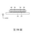
參照第5A圖及第5B圖,分別是根據本揭露的一些實施例繪示的製造感測裝置的各種階段的俯視示意圖及剖面示意圖。如第5A圖及第5B圖所示,形成第二電極層40在第一介電層30上。在一些實施例中,第二電極層40可包括彼此分離的第三電極40a及第四電極40b。在一些實施例用,用於形成第二電極層40的材料及形成方法可與用於形成第一電極層20的材料及形成方法相同或不同。在一些實施例用,第二電極層40與第一電極層20的形狀可為相同或不同。在一些實施例中,可藉由沿著第三方向D3的側面佈線(未顯示)連接第一電極層20及第二電極層40。在一些實施例中,第三電極40a可為正電極,且第四電極40b可為負電極。舉例而言,第一電極20a可與第三電極40a電性連接,且第二電極20b可與第四電極40b電性連接。Referring to FIG. 5A and FIG. 5B , there are respectively a schematic top view and a schematic cross-sectional view of various stages of manufacturing a sensing device according to some embodiments of the present disclosure. As shown in FIG. 5A and FIG. 5B , a
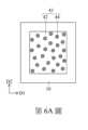
參照第6A圖及第6B圖,分別是根據本揭露的一些實施例繪示的製造感測裝置的各種階段的俯視示意圖及剖面示意圖。如第6A圖及第6B圖所示,可提供第二混合物41在第二電極層40及第一介電層30上。在一些實施例中,可藉由塗佈製程、3D列印製程、或其他合適的製程來提供第二混合物41至第二電極層40及第一介電層30上,然本揭露不限於此。在一些實施例中,第二混合物41可覆蓋第二電極層40的頂表面及側表面。第二混合物41可介於第二電極層40的第三電極40a及第四電極40b之間。第二混合物41可與第三電極40a及第四電極40b直接接觸。Referring to FIG. 6A and FIG. 6B , there are respectively a schematic top view and a schematic cross-sectional view of various stages of manufacturing a sensing device according to some embodiments of the present disclosure. As shown in FIG. 6A and FIG. 6B , a
在一些實施例中,第二混合物41可包括第二感測材料42及分散在第二感測材料42中的複數個第二粒子44。在一些實施例中,第二感測材料42與第一感測材料22可為相同或不同,且第二粒子44與第一粒子24可為相同或不同。在另一些實施例中,可省略第二粒子44,以形成實質上不具有孔洞的第二感測層。在一些實施例中,第二感測材料42與第一感測材料22可為不同,以使形成的第一感測層26及第二感測層可用於感測不同氣體。In some embodiments, the
參照第7A圖及第7B圖,分別是根據本揭露的一些實施例繪示的製造感測裝置的各種階段的俯視示意圖及剖面示意圖。如第7A圖及第7B圖所示,形成第二介電層50在第二混合物41上。在一些實施例中,用於形成第二介電層50的材料及形成方法可與用於形成第一介電層30的材料及形成方法相同或不同。7A and 7B are top view and cross-sectional views of various stages of manufacturing a sensing device according to some embodiments of the present disclosure. As shown in FIG. 7A and FIG. 7B , a
如第7B圖所示,在一些實施例中,執行第二熱處理製程P2,以移除第二混合物41中的第二粒子44,且保留第二混合物41中的第二感測材料42,並形成第二感測層46(如第8圖所示)。在一些實施例中,第二介電層50暴露第二感測層46的側表面。在一些實施例中,第二熱處理製程P2的溫度可介於第二粒子44的燃點(或熱分解溫度)與第二感測材料42的退火溫度之間。As shown in FIG. 7B , in some embodiments, a second heat treatment process P2 is performed to remove the
在一些實施例中,在形成第二介電層50在第二混合物41上之後,執行第二熱處理製程P2。在另一些實施例中,在形成第二介電層50在第二混合物41上之前,執行第二熱處理製程P2。在又一些實施例中,可省略第一熱處理製程P1,並執行第二熱處理製程P2,以藉由第二熱處理製程P2來移除第二混合物41中的第二粒子44及第一混合物21中的第一粒子24。在此實施例中,第二熱處理製程P2的溫度可大於第一粒子24的燃點(或熱分解溫度)及第二粒子44的燃點(或熱分解溫度)。在又一些實施例中,當第二混合物41中實質上不包括第二粒子44時,可執行第二熱處理製程P2,以形成第二感測層46並使第二感測層46退火。在此實施例中,第二熱處理製程P2的溫度可為第二感測層46的退火溫度。In some embodiments, the second heat treatment process P2 is performed after forming the
參照第8圖,其是根據本揭露的一些實施例繪示的感測裝置1的剖面示意圖。如第8圖所示,在一些實施例中,重複執行前述步驟,以形成第三電極層60在第二介電層50上,形成第三感測層66在第三電極層60上,且形成第三介電層70在第三感測層66上。接著,形成第四電極層80在第三介電層70上,且形成第四感測層86在第四電極層80上。在一些實施例中,第三電極層60及第四電極層80的材料及形成方法可與第一電極層20的材料及形成方法相同或不同。第三感測層66及第四感測層86的材料及形成方法可與第一感測層26及第二感測層46的材料及形成方法相同或不同。第三介電層70的材料及形成方法可與第一介電層30的材料及形成方法相同或不同。需說明的是,感測裝置1中可包括任意數量的感測單元。舉例而言,感測裝置1中可包括2個、3個、4個(如第8圖所示)、5個、6個、7個、8個、9個、10個、15個、20個或其他合適的數值的感測單元。Referring to FIG. 8 , it is a cross-sectional schematic diagram of a sensing device 1 according to some embodiments of the present disclosure. As shown in FIG. 8 , in some embodiments, the aforementioned steps are repeatedly performed to form a
如第8圖所示,在一些實施例中,形成覆蓋層90在基板10上,以獲得感測裝置1。在一些實施例中,覆蓋層90可包圍第一電極層20至第四電極層80、第一感測層26至第四感測層86及第一介電層30至第三介電層70。在一些實施例中,覆蓋層90可用於預防外力衝擊感測裝置1而使得感測裝置1損壞,因此覆蓋層90可作為感測裝置1的保護層。在一些實施例中,覆蓋層90可具有開口92,使得待測氣體G穿過開口92而與第一感測層26至第四感測層86接觸。As shown in FIG. 8 , in some embodiments, a
在一些實施例中,在感測裝置1中,相鄰的兩個感測層可在基板10的法線方向(亦即,第三方向D3)重疊。舉例而言,第一感測層26及第二感測層46在基板10的法線方向(亦即,第三方向D3)上重疊。據此,能夠減少感測裝置1的裝置面積。In some embodiments, in the sensing device 1, two adjacent sensing layers may overlap in the normal direction (i.e., the third direction D3) of the
在一些實施例中,在感測裝置1中,相鄰的兩個感測層中較遠離基板10的感測層稱為上層的感測層(upper sensing layer),且相鄰的兩個感測層中較接近基板10的感測層稱為下層的感測層(lower sensing layer)。在一些實施例中,在感測裝置1中,上層的感測層的面積可大於或等於下層的感測層的面積的50%。舉例而言,第一感測層26及第二感測層46相鄰,且相較於第一感測層26,第二感測層26較遠離基板10。因此,第二感測層46的面積可大於或等於第一感測層26的面積的50%。舉例而言,第二感測層46的面積可為第一感測層26的面積的50%、60%、70%、80%、90%、95%、100%、或前述範圍中的其他數值或數值範圍,然本揭露不限於此。若上層的感測層的面積小於下層的感測層的面積的50%,則可能造成上層的感測層的感測面積不足。在一些實施例中,第二感測層46在基板10上的投影面積可小於或等於第一感測層26在基板10上的投影面積。在一些實施例中,第二感測層46在基板10上的投影位在第一感測層26在基板10上的投影之中。In some embodiments, in the sensing device 1, the sensing layer farther from the
在一些實施例中,在感測裝置1中,上層的感測層可暴露下層的感測層的頂表面的一部分。舉例而言,第二感測層46可暴露第一感測層26的頂表面的一部分。據此,上層的感測層的面積可小於下層的感測層的面積,從而使得下層的感測層的暴露表面進一步接觸待測氣體G,而增加待測氣體G與下層的感測層的接觸面積。換句話說,使得感測裝置1中的每一層感測層都能有效地進行感測,並減少感測裝置1的裝置面積。In some embodiments, in the sensing device 1, the upper sensing layer may expose a portion of the top surface of the lower sensing layer. For example, the
在一些實施例中,在感測裝置1中,下層的感測層的孔洞密度可大於或等於上層的感測層的孔洞密度。舉例而言,第一感測層26及第二感測層46相鄰,且相較於第二感測層46,第一感測層26較接近基板10。因此,第一感測層26的孔洞密度可大於或等於第二感測層46的孔洞密度。舉例而言,上層的感測層與下層的感測層的孔洞密度的差值(|上層的感測層的孔洞密度-下層的感測層的孔洞密度|)可為0、10%、20%、30%、40%、或前述範圍中的其他數值或數值範圍,然本揭露不限於此。據此,下層的感測層的孔洞密度可大於上層的感測層的孔洞密度,使得待測氣體G能夠接觸下層的感測層。換句話說,使得感測裝置1中的每一層感測層都能有效地進行感測,並減少感測裝置1的裝置面積。In some embodiments, in the sensing device 1, the hole density of the lower sensing layer may be greater than or equal to the hole density of the upper sensing layer. For example, the
在一些實施例中,在感測裝置1中,各感測層可包括彼此不同的感測材料,以感測不同氣體。舉例而言,第二感測層46可設置於第一感測層26及第三感測層66之間,且第三感測層66、第二感測層46及第一感測層26的材料彼此不同。在一些實施例中,在感測裝置1中,第一感測層26可用於感測氨氣(ammonia);第二感測層46及第三感測層66可用於感測有機氣體(organic gas);且第四感測層86可用於感測水氣(water vapor)。在一些實施例中,在感測裝置1中,第一感測層26可包括氧化鉬,第二感測層46可包括碳黑,第三感測層66可包括氧化鎳,且第四感測層86可包括二氧化錫,以用於感測水氣、乙醇、丙酮及異丙醇。In some embodiments, in the sensing device 1, each sensing layer may include different sensing materials to sense different gases. For example, the
在下文中,以相同或相似的元件符號代表相同或相似的元件,且省略重複地描述。In the following, the same or similar elements are represented by the same or similar reference numerals, and repeated descriptions are omitted.
參照第9圖,其是根據本揭露的一些實施例繪示的感測裝置2的剖面示意圖。如第9圖所示,在一些實施例中,在感測裝置2中,第四感測層86可實質上不具有孔洞,因此第四感測層86的孔洞密度可實質上為0。由於第四感測層86的頂表面可直接接觸待測氣體G,因此可減少第四感測層86的面積,並藉由第四感測層86暴露第三感測層66的頂表面的一部分,從而提升第三感測層66與待測氣體G的接觸面積。在一些實施例中,第四感測層86的面積為第三感測層66的面積的70%,且第四感測層86的孔洞密度與第三感測層66的孔洞密度的差值為30%。在一些實施例中,第三感測層66的孔洞密度可為30%,第二感測層46的孔洞密度可為70%,且第一感測層26的孔洞密度可為70%。換句話說,第一感測層26的孔洞密度可與第二感測層46的孔洞密度實質上相同,且第一感測層26的孔洞密度可大於第三感測層66的孔洞密度。第三感測層66的孔洞密度可大於第四感測層86的孔洞密度。Referring to FIG. 9 , it is a schematic cross-sectional view of a sensing device 2 according to some embodiments of the present disclosure. As shown in FIG. 9 , in some embodiments, in the sensing device 2, the
參照第10圖,其是根據本揭露的一些實施例繪示的感測裝置3的剖面示意圖。如第10圖所示,在一些實施例中,感測裝置3可包括基底電極層12、基底感測層14及基底介電層16。在一些實施例中,基底電極層12可設置在基板10上。基底感測層14可設置在基底電極層12及基板10上。基底介電層16可設置在基底感測層14的側表面及頂表面上。因此,第一感測層26可設置在介於基底感測層14及第二感測層46之間。在一些實施例中,基底介電層16及基板10可包圍基底感測層14,而封閉(enclose)基底感測層14。因此,藉由基底介電層16隔離待測氣體G與基底感測層14,使得待測氣體G與基底感測層14無法彼此接觸。在一些實施例中,基底電極層12的材料及形成方法可與第一電極層20的材料及形成方法相同或不同。基底感測層14的材料及形成方法可與第一感測層26或第二感測層46的材料及形成方法相同或不同。基底介電層16的材料及形成方法可與第一介電層30的材料及形成方法相同或不同。Referring to FIG. 10 , it is a schematic cross-sectional view of a sensing device 3 according to some embodiments of the present disclosure. As shown in FIG. 10 , in some embodiments, the sensing device 3 may include a
在一些實施例中,基底感測層14可與第一感測層26、第二感測層46或第三感測層66的材料相同,而作為第一感測層26、第二感測層46或第三感測層66的共軛層(conjugate layer)。在一些實施例中,當基底感測層14與第一感測層26的材料相同時,基底感測層14能夠提供第一感測層26中的第一感測材料22未接觸待測氣體G時的電性特徵,以作為第一感測層26的基線(baseline)。在此實施例中,第一感測層26的孔洞密度可為70%,且基底感測層14的孔洞密度可為70%(未顯示),第二感測層46的孔洞密度可為70%,且第三感測層66的孔洞密度可為0。換句話說,第一感測層26的孔洞密度可與基底感測層14的孔洞密度實質上相同,第一感測層26的孔洞密度可與第二感測層46的孔洞密度實質上相同,且第一感測層26的孔洞密度可大於第三感測層66的孔洞密度。In some embodiments, the
在另一些實施例中,當基底感測層14與第三感測層66的材料相同時,基底感測層14及第三感測層66的孔洞密度可皆為0,第二感測層46的孔洞密度可為70%,第一感測層26的孔洞密度可為70%。換句話說,第一感測層26的孔洞密度可與第二感測層46的孔洞密度實質上相同,且第一感測層26的孔洞密度可大於第三感測層66的孔洞密度。In other embodiments, when the
綜上所述,根據本揭露的一些實施例,本揭露藉由在垂直方向上設置具有複數個孔洞的第一感測層及第二感測層,來提供垂直堆疊式感測裝置。在本揭露中,藉由移除粒子(例如,第一粒子)來形成複數個孔洞,來微縮化感測裝置。再者,本揭露藉由調整粒子直徑、孔洞密度、各感測層的面積比例及/或堆疊方式,來控制感測裝置的感測特性。據此,本揭露提供經改良的感測裝置及其製造方法。In summary, according to some embodiments of the present disclosure, the present disclosure provides a vertically stacked sensing device by arranging a first sensing layer and a second sensing layer having a plurality of holes in a vertical direction. In the present disclosure, a plurality of holes are formed by removing particles (e.g., first particles) to miniaturize the sensing device. Furthermore, the present disclosure controls the sensing characteristics of the sensing device by adjusting the particle diameter, the hole density, the area ratio of each sensing layer and/or the stacking method. Accordingly, the present disclosure provides an improved sensing device and a manufacturing method thereof.
雖然本揭露的實施例及其優點已揭露如上,但應該瞭解的是,任何所屬技術領域中具有通常知識者,在不脫離本揭露之精神及範圍內,當可作更動、替代與潤飾。本揭露實施例之間的特徵只要不違背發明精神或相衝突,均可任意混合搭配使用。此外,本揭露之保護範圍並未侷限於說明書內所述特定實施例中的製程、機器、製造、物質組成、裝置、方法及步驟,任何所屬技術領域中具有通常知識者可從本揭露揭示內容中理解現行或未來所發展出的製程、機器、製造、物質組成、裝置、方法及步驟,只要可以在此處所述實施例中實施實質上相同功能或獲得實質上相同結果皆可根據本揭露使用。因此,本揭露之保護範圍包括上述製程、機器、製造、物質組成、裝置、方法及步驟。本揭露之保護範圍當視申請專利範圍所界定者為準。本揭露的任一實施例或請求項不須達成本揭露所公開的全部目的、優點及/或特點。Although the embodiments and advantages of the present disclosure have been disclosed as above, it should be understood that any person with ordinary knowledge in the relevant technical field can make changes, substitutions and embellishments without departing from the spirit and scope of the present disclosure. The features between the embodiments of the present disclosure can be mixed and matched as long as they do not violate the spirit of the invention or conflict with each other. In addition, the scope of protection of the present disclosure is not limited to the processes, machines, manufacturing, material compositions, devices, methods and steps in the specific embodiments described in the specification. Any person with ordinary knowledge in the relevant technical field can understand the current or future developed processes, machines, manufacturing, material compositions, devices, methods and steps from the content of the present disclosure, as long as they can implement substantially the same functions or obtain substantially the same results in the embodiments described here, they can be used according to the present disclosure. Therefore, the protection scope of the present disclosure includes the above-mentioned processes, machines, manufactures, material compositions, devices, methods and steps. The protection scope of the present disclosure shall be determined by the scope of the patent application. Any embodiment or claim of the present disclosure does not need to achieve all the purposes, advantages and/or features disclosed in the present disclosure.
以上概述數個實施例,以便在本揭露所屬技術領域中具有通常知識者可以更理解本揭露實施例的觀點。在本揭露所屬技術領域中具有通常知識者應該理解,他們能以本揭露實施例為基礎,設計或修改其他製程和結構,以達到與在此介紹的實施例相同之目的及/或優勢。在本揭露所屬技術領域中具有通常知識者也應該理解到,此類等效的製程和結構並無悖離本揭露的精神與範圍,且他們能在不違背本揭露之精神和範圍之下,做各式各樣的改變、取代和替換。Several embodiments are summarized above so that those with ordinary knowledge in the art to which the present disclosure belongs can better understand the perspectives of the embodiments of the present disclosure. Those with ordinary knowledge in the art to which the present disclosure belongs should understand that they can design or modify other processes and structures based on the embodiments of the present disclosure to achieve the same purposes and/or advantages as the embodiments introduced herein. Those with ordinary knowledge in the art to which the present disclosure belongs should also understand that such equivalent processes and structures do not deviate from the spirit and scope of the present disclosure, and they can make various changes, substitutions and replacements without violating the spirit and scope of the present disclosure.
1, 2, 3:感測裝置1, 2, 3: Sensing device
10:基板10: Substrate
12:基底電極層12: Base electrode layer
14:基底感測層14: Base sensing layer
16:基底介電層16: Base dielectric layer
20:第一電極層20: First electrode layer
20a:第一電極20a: first electrode
20b:第二電極20b: Second electrode
21:第一混合物21: First mixture
22:第一感測材料22: First sensing material
24:第一粒子24: The First Particle
25:孔洞25: Holes
26:第一感測層26: First sensing layer
30:第一介電層30: First dielectric layer
40:第二電極層40: Second electrode layer
40a:第三電極40a: third electrode
40b:第四電極40b: fourth electrode
41:第二混合物41: Second mixture
42:第二感測材料42: Second sensing material
44:第二粒子44: Second Particle
46:第二感測層46: Second sensing layer
50:第二介電層50: Second dielectric layer
60:第三電極層60: Third electrode layer
66:第三感測層66: Third sensing layer
70:第三介電層70: Third dielectric layer
80:第四電極層80: Fourth electrode layer
86:第四感測層86: Fourth sensing layer
90:覆蓋層90: Covering layer
92:開口92: Open
A-A’:線段A-A’: line segment
D1:第一方向D1: First direction
D2:第二方向D2: Second direction
D3:第三方向D3: Third direction
G:待測氣體G: Gas to be tested
P1:第一熱處理製程P1: First heat treatment process
P2:第二熱處理製程P2: Second heat treatment process
藉由以下的詳述配合所附圖式,我們能更加理解本揭露實施例的觀點。值得注意的是,根據工業上的標準慣例,一些部件(feature)可能沒有按照比例繪製。事實上,為了能清楚地討論,不同部件的尺寸可能被增加或減少。 第1A圖及第1B圖分別是根據本揭露的一些實施例繪示的製造感測裝置的各種階段的俯視示意圖及剖面示意圖。 第2A圖及第2B圖分別是根據本揭露的一些實施例繪示的製造感測裝置的各種階段的俯視示意圖及剖面示意圖。 第3A圖及第3B圖分別是根據本揭露的一些實施例繪示的製造感測裝置的各種階段的俯視示意圖及剖面示意圖。 第4A圖及第4B圖分別是根據本揭露的一些實施例繪示的製造感測裝置的各種階段的俯視示意圖及剖面示意圖。 第5A圖及第5B圖分別是根據本揭露的一些實施例繪示的製造感測裝置的各種階段的俯視示意圖及剖面示意圖。 第6A圖及第6B圖分別是根據本揭露的一些實施例繪示的製造感測裝置的各種階段的俯視示意圖及剖面示意圖。 第7A圖及第7B圖分別是根據本揭露的一些實施例繪示的製造感測裝置的各種階段的俯視示意圖及剖面示意圖。 第8圖至第10圖分別是根據本揭露的一些實施例繪示的感測裝置的剖面示意圖。Through the following detailed description and the attached drawings, we can better understand the viewpoints of the embodiments of the present disclosure. It is worth noting that according to standard industrial practices, some features may not be drawn in proportion. In fact, in order to clearly discuss, the sizes of different features may be increased or reduced.Figures 1A and 1B are respectively a top view and a cross-sectional view of various stages of manufacturing a sensing device according to some embodiments of the present disclosure.Figures 2A and 2B are respectively a top view and a cross-sectional view of various stages of manufacturing a sensing device according to some embodiments of the present disclosure.Figures 3A and 3B are respectively a top view and a cross-sectional view of various stages of manufacturing a sensing device according to some embodiments of the present disclosure.FIG. 4A and FIG. 4B are respectively schematic top views and schematic cross-sectional views of various stages of manufacturing a sensing device according to some embodiments of the present disclosure.FIG. 5A and FIG. 5B are respectively schematic top views and schematic cross-sectional views of various stages of manufacturing a sensing device according to some embodiments of the present disclosure.FIG. 6A and FIG. 6B are respectively schematic top views and schematic cross-sectional views of various stages of manufacturing a sensing device according to some embodiments of the present disclosure.FIG. 7A and FIG. 7B are respectively schematic top views and schematic cross-sectional views of various stages of manufacturing a sensing device according to some embodiments of the present disclosure.FIG. 8 to FIG. 10 are respectively schematic cross-sectional views of a sensing device according to some embodiments of the present disclosure.
1:感測裝置1:Sensing device
10:基板10: Substrate
20:第一電極層20: First electrode layer
26:第一感測層26: First sensing layer
30:第一介電層30: First dielectric layer
40:第二電極層40: Second electrode layer
46:第二感測層46: Second sensing layer
50:第二介電層50: Second dielectric layer
60:第三電極層60: Third electrode layer
66:第三感測層66: The third sensing layer
70:第三介電層70: Third dielectric layer
80:第四電極層80: Fourth electrode layer
86:第四感測層86: The fourth sensing layer
90:覆蓋層90: Covering layer
92:開口92: Open mouth
G:待測氣體G: Gas to be tested
D1:第一方向D1: First direction
D3:第三方向D3: Third direction
Claims (10)
Translated fromChinesePriority Applications (3)
| Application Number | Priority Date | Filing Date | Title |
|---|---|---|---|
| TW112104897ATWI849738B (en) | 2023-02-13 | 2023-02-13 | Sensing device and manufacturing method thereof |
| CN202310346356.XACN118483284A (en) | 2023-02-13 | 2023-04-03 | Sensing device and method of manufacturing the same |
| US18/308,353US20240274537A1 (en) | 2023-02-13 | 2023-04-27 | Sensing device and manufacturing method thereof |
Applications Claiming Priority (1)
| Application Number | Priority Date | Filing Date | Title |
|---|---|---|---|
| TW112104897ATWI849738B (en) | 2023-02-13 | 2023-02-13 | Sensing device and manufacturing method thereof |
Publications (2)
| Publication Number | Publication Date |
|---|---|
| TWI849738Btrue TWI849738B (en) | 2024-07-21 |
| TW202433052A TW202433052A (en) | 2024-08-16 |
Family
ID=92192597
Family Applications (1)
| Application Number | Title | Priority Date | Filing Date |
|---|---|---|---|
| TW112104897ATWI849738B (en) | 2023-02-13 | 2023-02-13 | Sensing device and manufacturing method thereof |
Country Status (3)
| Country | Link |
|---|---|
| US (1) | US20240274537A1 (en) |
| CN (1) | CN118483284A (en) |
| TW (1) | TWI849738B (en) |
Citations (3)
| Publication number | Priority date | Publication date | Assignee | Title |
|---|---|---|---|---|
| US6513362B1 (en)* | 1997-10-10 | 2003-02-04 | Nanoproducts Corporation | Low-cost multi-laminate sensors |
| TW201616127A (en)* | 2014-10-31 | 2016-05-01 | 國立交通大學 | Vertical sensor having multiple layers and manufacturing method thereof, and sensing system and sensing method using the vertical sensor having multiple layers |
| TW201830657A (en)* | 2017-02-13 | 2018-08-16 | 華邦電子股份有限公司 | Multifunctional sensor |
- 2023
- 2023-02-13TWTW112104897Apatent/TWI849738B/enactive
- 2023-04-03CNCN202310346356.XApatent/CN118483284A/enactivePending
- 2023-04-27USUS18/308,353patent/US20240274537A1/enactivePending
Patent Citations (3)
| Publication number | Priority date | Publication date | Assignee | Title |
|---|---|---|---|---|
| US6513362B1 (en)* | 1997-10-10 | 2003-02-04 | Nanoproducts Corporation | Low-cost multi-laminate sensors |
| TW201616127A (en)* | 2014-10-31 | 2016-05-01 | 國立交通大學 | Vertical sensor having multiple layers and manufacturing method thereof, and sensing system and sensing method using the vertical sensor having multiple layers |
| TW201830657A (en)* | 2017-02-13 | 2018-08-16 | 華邦電子股份有限公司 | Multifunctional sensor |
Also Published As
| Publication number | Publication date |
|---|---|
| TW202433052A (en) | 2024-08-16 |
| CN118483284A (en) | 2024-08-13 |
| US20240274537A1 (en) | 2024-08-15 |
Similar Documents
| Publication | Publication Date | Title |
|---|---|---|
| US8421582B2 (en) | ESD protection device and manufacturing method therefor | |
| EP1723673B1 (en) | Method of making a semiconductor device | |
| CN103081033B (en) | Resistive device and method for manufacturing resistive device | |
| US6969565B2 (en) | Solid oxide fuel cell stack and method of manufacturing the same | |
| CN105190865B (en) | The manufacture method of semiconductor device and semiconductor device | |
| US20130283886A1 (en) | Particulate matter detection element and method of manufacturing same | |
| DE102009045428B4 (en) | Manufacturing method for a micromechanical component and micromechanical component | |
| TWI673726B (en) | Conductive composition, semiconductor element and solar cell element | |
| US20170131252A1 (en) | Micro heater, micro sensor and micro sensor manufacturing method | |
| EP2762866A1 (en) | CMOS gas sensor and method for manufacturing the same | |
| JP5971416B2 (en) | ESD protection device | |
| DE102015122668A1 (en) | Sensor for detecting electrically conductive and / or polarisable particles, sensor system, method for operating a sensor, method for producing such a sensor and use of such a sensor | |
| JP2020043336A (en) | Ceramic substrate, electrostatic chuck, method of manufacturing the same | |
| WO2010048782A1 (en) | Chip type fuse and its manufacturing method | |
| TWI849738B (en) | Sensing device and manufacturing method thereof | |
| KR100807217B1 (en) | Ceramic parts and manufacturing method thereof | |
| US10971321B2 (en) | Protection device and battery pack | |
| EP3403993A1 (en) | Semiconductor chip | |
| CN107731339A (en) | Conductive oxide sintered body for gas sensor, conductive oxide sintered body, wiring substrate, and gas sensor | |
| WO2017104564A1 (en) | Gas sensor element and gas sensor | |
| CN109644556B (en) | Ceramic electronic component and method for manufacturing ceramic electronic component | |
| CN108335988A (en) | A method of manufacturing a silicon capacitor | |
| TWI769542B (en) | Gas detecting structure | |
| CN108962516B (en) | Chip resistor and method for manufacturing the same | |
| CN207368416U (en) | ESD protection device |