TWI848574B - Semiconductor structure and manufacturing method thereof - Google Patents
Semiconductor structure and manufacturing method thereofDownload PDFInfo
- Publication number
- TWI848574B TWI848574BTW112105968ATW112105968ATWI848574BTW I848574 BTWI848574 BTW I848574BTW 112105968 ATW112105968 ATW 112105968ATW 112105968 ATW112105968 ATW 112105968ATW I848574 BTWI848574 BTW I848574B
- Authority
- TW
- Taiwan
- Prior art keywords
- substrate
- conductive liner
- layer
- material layer
- forming
- Prior art date
Links
- 239000004065semiconductorSubstances0.000titleclaimsabstractdescription55
- 238000004519manufacturing processMethods0.000titleclaimsdescription21
- 239000000758substrateSubstances0.000claimsabstractdescription102
- 238000002955isolationMethods0.000claimsabstractdescription63
- 239000000463materialSubstances0.000claimsdescription81
- 238000000034methodMethods0.000claimsdescription52
- 229910021420polycrystalline siliconInorganic materials0.000claimsdescription13
- 229920005591polysiliconPolymers0.000claimsdescription13
- 238000005468ion implantationMethods0.000claimsdescription12
- 239000002184metalSubstances0.000claimsdescription5
- 229910021332silicideInorganic materials0.000claimsdescription5
- FVBUAEGBCNSCDD-UHFFFAOYSA-Nsilicide(4-)Chemical compound[Si-4]FVBUAEGBCNSCDD-UHFFFAOYSA-N0.000claimsdescription5
- 239000010410layerSubstances0.000description161
- 239000003989dielectric materialSubstances0.000description20
- VYPSYNLAJGMNEJ-UHFFFAOYSA-NSilicium dioxideChemical compoundO=[Si]=OVYPSYNLAJGMNEJ-UHFFFAOYSA-N0.000description15
- 229910052814silicon oxideInorganic materials0.000description15
- 229910052581Si3N4Inorganic materials0.000description9
- 229920002120photoresistant polymerPolymers0.000description9
- HQVNEWCFYHHQES-UHFFFAOYSA-Nsilicon nitrideChemical compoundN12[Si]34N5[Si]62N3[Si]51N64HQVNEWCFYHHQES-UHFFFAOYSA-N0.000description9
- 238000001312dry etchingMethods0.000description7
- 238000005229chemical vapour depositionMethods0.000description6
- 239000004020conductorSubstances0.000description5
- 239000002131composite materialSubstances0.000description4
- 238000001459lithographyMethods0.000description4
- 230000003647oxidationEffects0.000description4
- 238000007254oxidation reactionMethods0.000description4
- 239000002356single layerSubstances0.000description4
- 238000005530etchingMethods0.000description3
- 238000001039wet etchingMethods0.000description3
- XUIMIQQOPSSXEZ-UHFFFAOYSA-NSiliconChemical compound[Si]XUIMIQQOPSSXEZ-UHFFFAOYSA-N0.000description2
- 238000005498polishingMethods0.000description2
- 229910052710siliconInorganic materials0.000description2
- 239000010703siliconSubstances0.000description2
- 239000000126substanceSubstances0.000description2
- 101100012902Saccharomyces cerevisiae (strain ATCC 204508 / S288c) FIG2 geneProteins0.000description1
- 101100233916Saccharomyces cerevisiae (strain ATCC 204508 / S288c) KAR5 geneProteins0.000description1
- 230000015572biosynthetic processEffects0.000description1
- 230000003247decreasing effectEffects0.000description1
- 238000012986modificationMethods0.000description1
- 230000004048modificationEffects0.000description1
- 238000005240physical vapour depositionMethods0.000description1
- 238000004528spin coatingMethods0.000description1
Images


Landscapes
- Semiconductor Memories (AREA)
- Non-Volatile Memory (AREA)
- Element Separation (AREA)
- Internal Circuitry In Semiconductor Integrated Circuit Devices (AREA)
Abstract
Description
Translated fromChinese本發明是有關於一種半導體結構及其製造方法,且特別是有關於一種具有埋入式導線(buried conductive line)的半導體結構及其製造方法。The present invention relates to a semiconductor structure and a manufacturing method thereof, and in particular to a semiconductor structure with buried conductive lines and a manufacturing method thereof.
一些半導體元件具有埋入式導線。舉例來說,在快閃記憶體(flash memory)中,可使用埋入式導線來作為埋入式源極線。然而,在藉由自對準源極製程(self-aligned source (SAS) process)來形成埋入式源極線時,會導致有效閘極長度(effective gate length)大幅地縮短,因此無法進一步地縮小記憶體元件的尺寸。Some semiconductor devices have buried wires. For example, in flash memory, buried wires can be used as buried source lines. However, when the buried source line is formed by a self-aligned source (SAS) process, the effective gate length is greatly shortened, so the size of the memory device cannot be further reduced.
本發明提供一種半導體結構及其製造方法,其有助於進一步地縮小半導體元件的尺寸。The present invention provides a semiconductor structure and a manufacturing method thereof, which are helpful to further reduce the size of semiconductor devices.
本發明提出一種半導體結構,包括基底、隔離結構與埋入式導線。隔離結構位在基底中。埋入式導線位在基底中。埋入式導線包括導電襯層與第一摻雜區。導電襯層位在隔離結構與基底之間。第一摻雜區位在隔離結構旁的基底中。第一摻雜區電性連接於導電襯層。The present invention provides a semiconductor structure, including a substrate, an isolation structure and a buried wire. The isolation structure is located in the substrate. The buried wire is located in the substrate. The buried wire includes a conductive liner and a first doped region. The conductive liner is located between the isolation structure and the substrate. The first doped region is located in the substrate next to the isolation structure. The first doped region is electrically connected to the conductive liner.
依照本發明的一實施例所述,在上述半導體結構中,第一摻雜區的頂面可為平坦表面。According to an embodiment of the present invention, in the semiconductor structure, the top surface of the first doped region can be a flat surface.
依照本發明的一實施例所述,在上述半導體結構中,導電襯層的材料例如是摻雜多晶矽或金屬矽化物(metal silicide)。According to an embodiment of the present invention, in the semiconductor structure, the material of the conductive liner is, for example, doped polysilicon or metal silicide.
依照本發明的一實施例所述,在上述半導體結構中,更可包括控制閘極、浮置閘極、第一介電層與第二介電層。控制閘極位在埋入式導線旁的基底上。浮置閘極位在控制閘極與基底之間。第一介電層位在控制閘極與浮置閘極之間。第二介電層位在浮置閘極與基底之間。According to an embodiment of the present invention, the semiconductor structure may further include a control gate, a floating gate, a first dielectric layer and a second dielectric layer. The control gate is located on the substrate next to the buried wire. The floating gate is located between the control gate and the substrate. The first dielectric layer is located between the control gate and the floating gate. The second dielectric layer is located between the floating gate and the substrate.
依照本發明的一實施例所述,在上述半導體結構中,更可包括第二摻雜區。第一摻雜區可位在控制閘極的一側的基底中,且第二摻雜區可位在控制閘極的另一側的基底中。According to an embodiment of the present invention, the semiconductor structure may further include a second doped region. The first doped region may be located in the substrate on one side of the control gate, and the second doped region may be located in the substrate on the other side of the control gate.
本發明提出一種半導體結構的製造方法,包括以下步驟。提供基底。在基底中形成隔離結構。在基底中形成埋入式導線。埋入式導線包括導電襯層與第一摻雜區。導電襯層位在隔離結構與基底之間。第一摻雜區位在隔離結構旁的基底中。第一摻雜區電性連接於導電襯層。The present invention provides a method for manufacturing a semiconductor structure, comprising the following steps: providing a substrate; forming an isolation structure in the substrate; forming a buried conductor in the substrate; the buried conductor includes a conductive liner and a first doped region; the conductive liner is located between the isolation structure and the substrate; the first doped region is located in the substrate next to the isolation structure; and the first doped region is electrically connected to the conductive liner.
依照本發明的一實施例所述,在上述半導體結構的製造方法中,基底可包括埋入式導線區。埋入式導線可位在埋入式導線區中。隔離結構與導電襯層的形成方法可包括以下步驟。在基底上形成墊層。在墊層上形成硬罩幕層。在硬罩幕層、墊層與基底中形成溝渠。移除硬罩幕層。在墊層上與溝渠中形成導電襯材料層。移除位在埋入式導線區的外部的導電襯材料層。形成填入溝渠的隔離材料層。埋入式導線區中的隔離材料層可位在導電襯材料層上。移除部分隔離材料層,而暴露出導電襯材料層。移除部分導電襯材料層,而形成導電襯層。在形成導電襯層之後,移除部分隔離材料層,而形成隔離結構。According to one embodiment of the present invention, in the manufacturing method of the above-mentioned semiconductor structure, the substrate may include a buried wire area. The buried wire may be located in the buried wire area. The method for forming an isolation structure and a conductive liner may include the following steps. A pad is formed on the substrate. A hard mask layer is formed on the pad. Trench is formed in the hard mask layer, the pad and the substrate. The hard mask layer is removed. A conductive liner material layer is formed on the pad and in the trench. The conductive liner material layer located outside the buried wire area is removed. An isolation material layer is formed to fill the trench. The isolation material layer in the buried wire area may be located on the conductive liner material layer. Removing part of the isolation material layer to expose the conductive liner material layer. Removing part of the conductive liner material layer to form a conductive liner. After forming the conductive liner, removing part of the isolation material layer to form an isolation structure.
依照本發明的一實施例所述,在上述半導體結構的製造方法中,更可包括以下步驟。移除墊層,而暴露出基底。在埋入式導線區旁的基底上形成控制閘極。在控制閘極與基底之間形成浮置閘極。在控制閘極與浮置閘極之間形成第一介電層。在浮置閘極與基底之間形成第二介電層。According to an embodiment of the present invention, the manufacturing method of the semiconductor structure may further include the following steps: removing the pad to expose the substrate; forming a control gate on the substrate next to the buried wiring region; forming a floating gate between the control gate and the substrate; forming a first dielectric layer between the control gate and the floating gate; and forming a second dielectric layer between the floating gate and the substrate.
依照本發明的一實施例所述,在上述半導體結構的製造方法中,更可包括以下步驟。對基底進行離子植入製程,而在控制閘極的一側的基底中形成第一摻雜區,且在控制閘極的另一側的基底中形成第二摻雜區。According to an embodiment of the present invention, the method for manufacturing the semiconductor structure may further include the following steps: performing an ion implantation process on the substrate to form a first doped region in the substrate on one side of the control gate and a second doped region in the substrate on the other side of the control gate.
依照本發明的一實施例所述,在上述半導體結構的製造方法中,離子植入製程可為垂直離子植入(vertical ion implantation)製程。According to an embodiment of the present invention, in the method for manufacturing the semiconductor structure, the ion implantation process may be a vertical ion implantation process.
基於上述,在本發明所提出的半導體結構及其製造方法中,埋入式導線位在基底中。埋入式導線包括導電襯層與第一摻雜區。導電襯層位在隔離結構與基底之間。第一摻雜區位在隔離結構旁的基底中。第一摻雜區電性連接於導電襯層。因此,本發明所提出的半導體結構及其製造方法有助於進一步地縮小半導體元件的尺寸,且可提升半導體元件的可靠度。Based on the above, in the semiconductor structure and the manufacturing method thereof proposed in the present invention, the buried wire is located in the substrate. The buried wire includes a conductive liner and a first doped region. The conductive liner is located between the isolation structure and the substrate. The first doped region is located in the substrate next to the isolation structure. The first doped region is electrically connected to the conductive liner. Therefore, the semiconductor structure and the manufacturing method thereof proposed in the present invention help to further reduce the size of semiconductor components and improve the reliability of semiconductor components.
為讓本發明的上述特徵和優點能更明顯易懂,下文特舉實施例,並配合所附圖式作詳細說明如下。In order to make the above features and advantages of the present invention more clearly understood, embodiments are given below and described in detail with reference to the accompanying drawings.
下文列舉實施例並配合附圖來進行詳細地說明,但所提供的實施例並非用以限制本發明所涵蓋的範圍。為了方便理解,在下述說明中相同的構件將以相同的符號標示來說明。此外,附圖僅以說明為目的,並未依照原尺寸作圖。另外,上視圖中的特徵與剖面圖中的特徵並非按相同比例繪製。事實上,為論述清晰起見,可任意增大或減小各種特徵的尺寸。The following examples are listed and illustrated in detail, but the examples provided are not intended to limit the scope of the present invention. For ease of understanding, the same components will be indicated by the same symbols in the following description. In addition, the drawings are for illustrative purposes only and are not drawn according to the original size. In addition, the features in the top view are not drawn to the same scale as the features in the cross-sectional view. In fact, the size of various features can be arbitrarily increased or decreased for the sake of clarity.
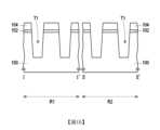
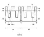
圖1A至圖1N為根據本發明的一些實施例的半導體結構的製造流程剖面圖。圖2為根據本發明的一些實施例的半導體結構的上視圖。圖2為圖1N的上視圖。圖1A至圖1N為沿著圖2中的I-I’剖面線與II-II’剖面線的剖面圖。圖3為沿著圖2中的III-III’剖面線的剖面圖。在本實施例的上視圖中,省略剖面圖中的部分構件,以清楚說明上視圖中的各構件之間的位置關係。FIG. 1A to FIG. 1N are cross-sectional views of the manufacturing process of the semiconductor structure according to some embodiments of the present invention. FIG. 2 is a top view of the semiconductor structure according to some embodiments of the present invention. FIG. 2 is a top view of FIG. 1N. FIG. 1A to FIG. 1N are cross-sectional views along the I-I’ section line and the II-II’ section line in FIG. 2. FIG. 3 is a cross-sectional view along the III-III’ section line in FIG. 2. In the top view of the present embodiment, some components in the cross-sectional view are omitted to clearly illustrate the positional relationship between the components in the top view.
請參照圖1A,提供基底100。在一些實施例中,基底100可包括埋入式導線區R1與非埋入式導線區R2。在一些實施例中,基底100可為半導體基底,如矽基底。1A , a
接著,可在基底100上形成墊層102。在一些實施例中,墊層102的材料例如是氧化矽。在一些實施例中,墊層102的形成方法例如是熱氧化法。Next, a
然後,可在墊層102上形成硬罩幕層104。在一些實施例中,硬罩幕層104的材料例如是氮化矽。在一些實施例中,硬罩幕層104的形成方法例如是化學氣相沉積法。Then, a
請參照圖1B,可在硬罩幕層104、墊層102與基底100中形成溝渠T1。在一些實施例中,可藉由微影製程與蝕刻製程(如,乾式蝕刻製程)對硬罩幕層104、墊層102與基底100進行圖案化,而形成溝渠T1。1B, a trench T1 may be formed in the
請參照圖1C,可移除硬罩幕層104。在一些實施例中,硬罩幕層104的移除方法例如是濕式蝕刻法。1C , the
請參照圖1D,可在墊層102上與溝渠T1中形成導電襯材料層106。在一些實施例中,導電襯材料層106可共形地形成在墊層102上與溝渠T1中。在一些實施例中,導電襯材料層106的材料例如是摻雜多晶矽或金屬矽化物。在一些實施例中,導電襯材料層106的形成方法例如是化學氣相沉積法或物理氣相沉積法。Referring to FIG. 1D , a conductive
請參照圖1E,可移除位在埋入式導線區R1的外部的導電襯材料層106。在一些實施例中,位在埋入式導線區R1的外部的導電襯材料層106的移除方法可包括以下步驟。首先,可形成圖案化光阻層108。圖案化光阻層108可位在埋入式導線區R1中的導電襯材料層106上,且可暴露出非埋入式導線區R2中的導電襯材料層106。在一些實施例中,可藉由微影製程來形成圖案化光阻層108。接著,可利用圖案化光阻層108作為罩幕,移除由圖案化光阻層108所暴露出的導電襯材料層106。在一些實施例中,由圖案化光阻層108所暴露出的導電襯材料層106的移除方法例如是乾式蝕刻法。Referring to FIG. 1E , the conductive
請參照圖1F,可移除圖案化光阻層108。在一些實施例中,圖案化光阻層108的移除方法例如是乾式剝離法(dry stripping)或濕式剝離法(wet stripping)。1F , the patterned
接著,可形成填入溝渠T1的隔離材料層110。埋入式導線區R1中的隔離材料層110可位在導電襯材料層106上,且非埋入式導線區R2中的隔離材料層110可位在基底100與墊層102上。隔離材料層110可為單層結構或多層結構。在一些實施例中,隔離材料層110的材料例如是氧化矽。在一些實施例中,隔離材料層110的形成方法例如是化學氣相沉積法或旋轉塗佈法。Next, an
請參照圖1G,可移除部分隔離材料層110,而暴露出導電襯材料層106。在一些實施例中,部分隔離材料層110的移除方法例如是乾式蝕刻法或化學機械研磨法。1G , a portion of the
請參照圖1H,可移除部分導電襯材料層106,而形成導電襯層106a。藉此,可在隔離材料層110與基底100之間形成導電襯層106a。在一些實施例中,導電襯層106a的材料例如是摻雜多晶矽或金屬矽化物。在一些實施例中,部分導電襯材料層106的移除方法例如是乾式蝕刻法。在一些實施例中,在移除部分導電襯材料層106的製程中,可同時移部分隔離材料層110。Referring to FIG. 1H , a portion of the conductive
請參照圖1I,在形成導電襯層106a之後,可移除部分隔離材料層110,而形成隔離結構110a。藉此,可在基底100中形成隔離結構110a。隔離結構110a可為單層結構或多層結構。在一些實施例中,隔離結構110a的材料例如是氧化矽。此外,可移除墊層102,而暴露出基底100。在一些實施例中,部分隔離材料層110與墊層102可藉由相同製程同時移除。在一些實施例中,部分隔離材料層110與墊層102的移除方法例如是濕式蝕刻法、乾式蝕刻法或化學機械研磨法。Referring to FIG. 1I , after forming the
請參照圖1J,可在基底100上形成介電材料層112。在一些實施例中,介電材料層112的材料例如是氧化矽。在一些實施例中,介電材料層112的形成方法例如是熱氧化法。舉例來說,在基底100為矽基底的情況下,可藉由熱氧化製程將部分基底100氧化成介電材料層112。此外,在導電襯層106a的材料為摻雜多晶矽的情況下,可藉由熱氧化製程將部分導電襯層106a氧化成介電材料層112。Referring to FIG. 1J , a
接著,可在介電材料層112與隔離結構110a上形成浮置閘極材料層114。在一些實施例中,浮置閘極材料層114的材料例如是摻雜多晶矽、未摻雜多晶矽或其組合。在一些實施例中,浮置閘極材料層114的形成方法例如是化學氣相沉積法。Next, a floating
請參照圖1K,可對浮置閘極材料層114進行圖案化。在一些實施例中,可藉由微影製程與蝕刻製程對浮置閘極材料層114進行圖案化。1K , the floating
請參照圖1L,可在浮置閘極材料層114上形成介電材料層116。介電材料層116更可形成在隔離結構110a上。在一些實施例中,介電材料層116可共形地形成在浮置閘極材料層114與隔離結構110a上。介電材料層116可為單層結構或多層結構。在一些實施例中,介電材料層116可為高介電常數材料(high-k material)層、氧化矽層、氧化矽層/氮化矽層/氧化矽層(ONO)的複合層或氮化矽層/氧化矽層/氮化矽層/氧化矽層/氮化矽層(NONON)的複合層。在一些實施例中,介電材料層116的形成方法例如是化學氣相沉積法。1L , a
接著,可在介電材料層116上形成控制閘極材料層118。在一些實施例中,控制閘極材料層118的材料例如是摻雜多晶矽、未摻雜多晶矽或其組合。在一些實施例中,控制閘極材料層118的形成方法例如是化學氣相沉積法。Next, a control
請參照圖1M,可對控制閘極材料層118、介電材料層116與浮置閘極材料層114進行圖案化,而形成控制閘極118a、介電層116a與浮置閘極114a。藉此,可在埋入式導線區R1旁的基底100上形成控制閘極118a,可在控制閘極118a與基底100之間形成浮置閘極114a,且可在控制閘極118a與浮置閘極114a之間形成介電層116a。在一些實施例中,控制閘極118a的材料例如是摻雜多晶矽。在一些實施例中,介電層116a可為單層結構或多層結構。在一些實施例中,介電層116a可為高介電常數材料、氧化矽層、氧化矽層/氮化矽層/氧化矽層(ONO)的複合層或氮化矽層/氧化矽層/氮化矽層/氧化矽層/氮化矽層(NONON)的複合層。在一些實施例中,浮置閘極114a的材料例如是摻雜多晶矽、未摻雜多晶矽或其組合。在一些實施例中,可藉由微影製程與蝕刻製程(如,乾式蝕刻製程)對控制閘極材料層118、介電材料層116與浮置閘極材料層114進行圖案化。1M, the control
接著,可對基底100進行離子植入製程,而在控制閘極118a的一側的基底100中形成摻雜區120,且在控制閘極118a的另一側的基底100中形成摻雜區122(圖2)。在一些實施例中,摻雜區120的頂面與摻雜區122的頂面可為平坦表面。在本實施例中,摻雜區120可用以作為源極區,且摻雜區122可用以作為汲極區,但本發明並不以此為限。在另一些實施例中,摻雜區120可用以作為汲極區,且摻雜區122可用以作為源極區。在一些實施例中,離子植入製程可為垂直離子植入製程。在一些實施例中,在形成摻雜區120的製程中,由於可僅藉由進行垂直離子植入製程來形成摻雜區120,且無須進行傾斜角離子植入製程,因此可減少離子植入製程對介電材料層112及介電層116a所造成的傷害,進而可提升半導體元件(如,記憶體元件)的可靠度。Then, the
藉由上述方法,可在基底100中形成埋入式導線124。埋入式導線124可位在埋入式導線區R1中。埋入式導線124包括導電襯層106a與摻雜區120。導電襯層106a位在隔離結構110a與基底100之間。摻雜區120位在隔離結構110a旁的基底100中。摻雜區120電性連接於導電襯層106a。在本實施例中,埋入式導線124可用以作為埋入式源極線,但本發明並不以此為限。在另一些實施例中,埋入式導線124可用以作為埋入式汲極線。由於埋入式導線124是由彼此電性連接的導電襯層106a與摻雜區120所形成,因此可防止有效閘極長度大幅地縮短,藉此可進一步地縮小半導體元件(如,記憶體元件)的尺寸。By the above method, a buried
然後,請參照圖1N,可藉由控制閘極118a作為罩幕,移除部分介電材料層112,而形成介電層112a。藉此,可在浮置閘極114a與基底100之間形成介電層112a。在一些實施例中,介電層112a的材料例如是氧化矽。在一些實施例中,部分介電材料層112的移除方法例如是濕式蝕刻法或乾式蝕刻法。此外,在移除部分介電材料層112的製程中,可同時移除部分隔離結構110a。Then, referring to FIG. 1N , a portion of the
此外,在後續製程中,可形成電性連接至埋入式導線124的內連線結構(未示出),且可形成電性連接至摻雜區122(圖2)的內連線結構(未示出),於此省略其說明。In addition, in subsequent processes, an internal connection structure (not shown) electrically connected to the buried
以下,藉由圖1N、圖2與圖3來說明上述實施例的半導體結構10。此外,雖然半導體結構10的形成方法是以上述方法為例來進行說明,但本發明並不以此為限。The
請參照圖1N、圖2與圖3,半導體結構10包括基底100、隔離結構110a與埋入式導線124。在一些實施例中,半導體結構10可為記憶體結構,如反或型快閃記憶體(NOR flash memory)結構。隔離結構110a位在基底100中。埋入式導線124位在基底100中。埋入式導線124包括導電襯層106a與摻雜區120。導電襯層106a位在隔離結構110a與基底100之間。摻雜區120位在隔離結構110a旁的基底100中。摻雜區120電性連接於導電襯層106a。在本實施例中,埋入式導線124可包括多個導電襯層106a與多個摻雜區120,但本發明並不以此為限。只要埋入式導線124包括至少一個導電襯層106a與至少一個摻雜區120,即屬於本發明所涵蓋的範圍。1N, 2 and 3, the
半導體結構10更可包括控制閘極118a、浮置閘極114a、介電層116a與介電層112a。控制閘極118a位在埋入式導線124旁的基底100上。浮置閘極114a位在控制閘極118a與基底100之間。介電層116a位在控制閘極118a與浮置閘極114a之間。介電層112a位在浮置閘極114a與基底100之間。The
半導體結構10更可包括摻雜區122。摻雜區120可位在控制閘極118a的一側的基底100中,且摻雜區122可位在控制閘極118a的另一側的基底100中。The
此外,半導體結構10中的各構件的詳細內容(如,材料與形成方法等)已於上述實施例進行詳盡地說明,於此不再說明。另外,半導體結構10中的各構件的數量並不限於圖中的數量。於此技術領域具有通常知識者可依據需求來調整半導體結構10中的各構件的數量。In addition, the details of each component in the semiconductor structure 10 (such as materials and formation methods, etc.) have been described in detail in the above embodiments and will not be described again here. In addition, the number of each component in the
基於上述實施例可知,在半導體結構10及其製造方法中,埋入式導線124位在基底100中。埋入式導線124包括導電襯層106a與摻雜區120。導電襯層106a位在隔離結構110a與基底100之間。摻雜區120位在隔離結構110a旁的基底100中。摻雜區120電性連接於導電襯層106a。因此,半導體結構10及其製造方法有助於進一步地縮小半導體元件(如,記憶體元件)的尺寸(如,面積),且可提升半導體元件的可靠度。Based on the above embodiments, it can be known that in the
綜上所述,在上述實施例的半導體結構及其製造方法中,埋入式導線位在基底中,且埋入式導線包括彼此電性連接的導電襯層與摻雜區,因此有助於進一步地縮小半導體元件的尺寸,且可提升半導體元件的可靠度。In summary, in the semiconductor structure and the manufacturing method thereof of the above-mentioned embodiments, the buried wire is located in the substrate, and the buried wire includes a conductive liner and a doped region electrically connected to each other, thereby helping to further reduce the size of the semiconductor device and improve the reliability of the semiconductor device.
雖然本發明已以實施例揭露如上,然其並非用以限定本發明,任何所屬技術領域中具有通常知識者,在不脫離本發明的精神和範圍內,當可作些許的更動與潤飾,故本發明的保護範圍當視後附的申請專利範圍所界定者為準。Although the present invention has been disclosed as above by the embodiments, they are not intended to limit the present invention. Any person with ordinary knowledge in the relevant technical field can make some changes and modifications without departing from the spirit and scope of the present invention. Therefore, the protection scope of the present invention shall be defined by the scope of the attached patent application.
10:半導體結構 100:基底 102:墊層 104:硬罩幕層 106:導電襯材料層 106a:導電襯層 108:圖案化光阻層 110:隔離材料層 110a:隔離結構 112, 116:介電材料層 112a, 116a:介電層 114:浮置閘極材料層 114a:浮置閘極 118:控制閘極材料層 118a:控制閘極 120, 122:摻雜區 124:埋入式導線 R1:埋入式導線區 R2:非埋入式導線區 T1:溝渠10: semiconductor structure100: substrate102: pad layer104: hard mask layer106: conductive
圖1A至圖1N為根據本發明的一些實施例的半導體結構的製造流程剖面圖。 圖2為根據本發明的一些實施例的半導體結構的上視圖。 圖3為沿著圖2中的III-III’剖面線的剖面圖。Figures 1A to 1N are cross-sectional views of the manufacturing process of a semiconductor structure according to some embodiments of the present invention.Figure 2 is a top view of a semiconductor structure according to some embodiments of the present invention.Figure 3 is a cross-sectional view along the III-III’ section line in Figure 2.
10:半導體結構10:Semiconductor structure
100:基底100: Base
106a:導電襯層106a: Conductive lining
110a:隔離結構110a: Isolation structure
112a,116a:介電層112a,116a: Dielectric layer
114a:浮置閘極114a: floating gate
118a:控制閘極118a: Control gate
120:摻雜區120: Mixed area
124:埋入式導線124: Embedded wire
R1:埋入式導線區R1: Embedded conductor area
R2:非埋入式導線區R2: Non-buried conductor area
T1:溝渠T1: Ditch
Claims (9)
Translated fromChinesePriority Applications (1)
| Application Number | Priority Date | Filing Date | Title |
|---|---|---|---|
| TW112105968ATWI848574B (en) | 2023-02-18 | 2023-02-18 | Semiconductor structure and manufacturing method thereof |
Applications Claiming Priority (1)
| Application Number | Priority Date | Filing Date | Title |
|---|---|---|---|
| TW112105968ATWI848574B (en) | 2023-02-18 | 2023-02-18 | Semiconductor structure and manufacturing method thereof |
Publications (2)
| Publication Number | Publication Date |
|---|---|
| TWI848574Btrue TWI848574B (en) | 2024-07-11 |
| TW202435724A TW202435724A (en) | 2024-09-01 |
Family
ID=92929259
Family Applications (1)
| Application Number | Title | Priority Date | Filing Date |
|---|---|---|---|
| TW112105968ATWI848574B (en) | 2023-02-18 | 2023-02-18 | Semiconductor structure and manufacturing method thereof |
Country Status (1)
| Country | Link |
|---|---|
| TW (1) | TWI848574B (en) |
Citations (5)
| Publication number | Priority date | Publication date | Assignee | Title |
|---|---|---|---|---|
| TW560055B (en)* | 2002-09-09 | 2003-11-01 | Macronix Int Co Ltd | Method of manufacturing a flash memory |
| TW200401436A (en)* | 2002-07-03 | 2004-01-16 | Macronix Int Co Ltd | Method of fabricating a buried bit line and memory device including the same |
| US20090315090A1 (en)* | 2008-06-23 | 2009-12-24 | Rolf Weis | Isolation Trenches with Conductive Plates |
| US20200152754A1 (en)* | 2015-12-23 | 2020-05-14 | SK Hynix Inc. | Semiconductor device having buried gate structure, method for manufacturing the same, and memory cell having the same |
| TW202226462A (en)* | 2020-12-29 | 2022-07-01 | 華邦電子股份有限公司 | Semiconductor memory structure and method for forming the same |
- 2023
- 2023-02-18TWTW112105968Apatent/TWI848574B/enactive
Patent Citations (5)
| Publication number | Priority date | Publication date | Assignee | Title |
|---|---|---|---|---|
| TW200401436A (en)* | 2002-07-03 | 2004-01-16 | Macronix Int Co Ltd | Method of fabricating a buried bit line and memory device including the same |
| TW560055B (en)* | 2002-09-09 | 2003-11-01 | Macronix Int Co Ltd | Method of manufacturing a flash memory |
| US20090315090A1 (en)* | 2008-06-23 | 2009-12-24 | Rolf Weis | Isolation Trenches with Conductive Plates |
| US20200152754A1 (en)* | 2015-12-23 | 2020-05-14 | SK Hynix Inc. | Semiconductor device having buried gate structure, method for manufacturing the same, and memory cell having the same |
| TW202226462A (en)* | 2020-12-29 | 2022-07-01 | 華邦電子股份有限公司 | Semiconductor memory structure and method for forming the same |
Also Published As
| Publication number | Publication date |
|---|---|
| TW202435724A (en) | 2024-09-01 |
Similar Documents
| Publication | Publication Date | Title |
|---|---|---|
| JP5330004B2 (en) | Manufacturing method of semiconductor device | |
| KR100375235B1 (en) | Sonos flash memory device and a method for fabricating the same | |
| JP4217406B2 (en) | Split gate flash memory device and manufacturing method thereof | |
| US20070026612A1 (en) | Method of fabricating flash memory device having self-aligned floating gate | |
| US7235442B2 (en) | Method for fabricating conductive line | |
| US20070187743A1 (en) | Semiconductor device and method of manufacturing the same | |
| JPH11135779A (en) | Semiconductor device and manufacturing method thereof | |
| JP2011199199A (en) | Semiconductor device and method for manufacturing the same | |
| TWI848574B (en) | Semiconductor structure and manufacturing method thereof | |
| TWI685085B (en) | Memory device and method of manufacturing the same | |
| JP4916177B2 (en) | Method for forming gate of flash memory device | |
| US7651912B2 (en) | Semiconductor device and method of fabricating the same | |
| JP3764177B2 (en) | Semiconductor memory device and manufacturing method thereof | |
| JP4822792B2 (en) | Semiconductor device and manufacturing method thereof | |
| JPH11330431A (en) | Manufacture for nonvolatile semiconductor memory device | |
| CN103208458B (en) | Manufacturing method of embedded flash memory | |
| US6562682B1 (en) | Method for forming gate | |
| CN111326516A (en) | Non-volatile memory structure and manufacturing method thereof | |
| JP2015056478A (en) | Semiconductor device and method of manufacturing semiconductor device | |
| CN111696989B (en) | Memory element and method for manufacturing the same | |
| JP2012129453A (en) | Semiconductor device and method of manufacturing semiconductor device | |
| US7122428B2 (en) | Device isolation method of semiconductor memory device and flash memory device fabricating method using the same | |
| JP4128737B2 (en) | Semiconductor device and method for manufacturing semiconductor memory device | |
| CN108110008B (en) | Semiconductor element and manufacturing method thereof and manufacturing method of memory | |
| TWI899484B (en) | Method of manufacturing semiconductor structure |