TWI847061B - Electromagnetic wave shielding film and shielding printed wiring board - Google Patents
Electromagnetic wave shielding film and shielding printed wiring boardDownload PDFInfo
- Publication number
- TWI847061B TWI847061BTW110135365ATW110135365ATWI847061BTW I847061 BTWI847061 BTW I847061BTW 110135365 ATW110135365 ATW 110135365ATW 110135365 ATW110135365 ATW 110135365ATW I847061 BTWI847061 BTW I847061B
- Authority
- TW
- Taiwan
- Prior art keywords
- conductive particles
- electromagnetic wave
- adhesive layer
- wave shielding
- flake
- Prior art date
Links
Images


Classifications
- H—ELECTRICITY
- H05—ELECTRIC TECHNIQUES NOT OTHERWISE PROVIDED FOR
- H05K—PRINTED CIRCUITS; CASINGS OR CONSTRUCTIONAL DETAILS OF ELECTRIC APPARATUS; MANUFACTURE OF ASSEMBLAGES OF ELECTRICAL COMPONENTS
- H05K1/00—Printed circuits
- H05K1/02—Details
- H05K1/0213—Electrical arrangements not otherwise provided for
- H05K1/0216—Reduction of cross-talk, noise or electromagnetic interference
- B—PERFORMING OPERATIONS; TRANSPORTING
- B32—LAYERED PRODUCTS
- B32B—LAYERED PRODUCTS, i.e. PRODUCTS BUILT-UP OF STRATA OF FLAT OR NON-FLAT, e.g. CELLULAR OR HONEYCOMB, FORM
- B32B27/00—Layered products comprising a layer of synthetic resin
- B32B27/18—Layered products comprising a layer of synthetic resin characterised by the use of special additives
- B—PERFORMING OPERATIONS; TRANSPORTING
- B32—LAYERED PRODUCTS
- B32B—LAYERED PRODUCTS, i.e. PRODUCTS BUILT-UP OF STRATA OF FLAT OR NON-FLAT, e.g. CELLULAR OR HONEYCOMB, FORM
- B32B7/00—Layered products characterised by the relation between layers; Layered products characterised by the relative orientation of features between layers, or by the relative values of a measurable parameter between layers, i.e. products comprising layers having different physical, chemical or physicochemical properties; Layered products characterised by the interconnection of layers
- B32B7/02—Physical, chemical or physicochemical properties
- B32B7/025—Electric or magnetic properties
- C—CHEMISTRY; METALLURGY
- C09—DYES; PAINTS; POLISHES; NATURAL RESINS; ADHESIVES; COMPOSITIONS NOT OTHERWISE PROVIDED FOR; APPLICATIONS OF MATERIALS NOT OTHERWISE PROVIDED FOR
- C09J—ADHESIVES; NON-MECHANICAL ASPECTS OF ADHESIVE PROCESSES IN GENERAL; ADHESIVE PROCESSES NOT PROVIDED FOR ELSEWHERE; USE OF MATERIALS AS ADHESIVES
- C09J201/00—Adhesives based on unspecified macromolecular compounds
- C—CHEMISTRY; METALLURGY
- C09—DYES; PAINTS; POLISHES; NATURAL RESINS; ADHESIVES; COMPOSITIONS NOT OTHERWISE PROVIDED FOR; APPLICATIONS OF MATERIALS NOT OTHERWISE PROVIDED FOR
- C09J—ADHESIVES; NON-MECHANICAL ASPECTS OF ADHESIVE PROCESSES IN GENERAL; ADHESIVE PROCESSES NOT PROVIDED FOR ELSEWHERE; USE OF MATERIALS AS ADHESIVES
- C09J7/00—Adhesives in the form of films or foils
- C09J7/30—Adhesives in the form of films or foils characterised by the adhesive composition
- C—CHEMISTRY; METALLURGY
- C09—DYES; PAINTS; POLISHES; NATURAL RESINS; ADHESIVES; COMPOSITIONS NOT OTHERWISE PROVIDED FOR; APPLICATIONS OF MATERIALS NOT OTHERWISE PROVIDED FOR
- C09J—ADHESIVES; NON-MECHANICAL ASPECTS OF ADHESIVE PROCESSES IN GENERAL; ADHESIVE PROCESSES NOT PROVIDED FOR ELSEWHERE; USE OF MATERIALS AS ADHESIVES
- C09J9/00—Adhesives characterised by their physical nature or the effects produced, e.g. glue sticks
- C09J9/02—Electrically-conducting adhesives
- H—ELECTRICITY
- H05—ELECTRIC TECHNIQUES NOT OTHERWISE PROVIDED FOR
- H05K—PRINTED CIRCUITS; CASINGS OR CONSTRUCTIONAL DETAILS OF ELECTRIC APPARATUS; MANUFACTURE OF ASSEMBLAGES OF ELECTRICAL COMPONENTS
- H05K1/00—Printed circuits
- H05K1/02—Details
- H05K1/0213—Electrical arrangements not otherwise provided for
- H05K1/0216—Reduction of cross-talk, noise or electromagnetic interference
- H05K1/0218—Reduction of cross-talk, noise or electromagnetic interference by printed shielding conductors, ground planes or power plane
- H—ELECTRICITY
- H05—ELECTRIC TECHNIQUES NOT OTHERWISE PROVIDED FOR
- H05K—PRINTED CIRCUITS; CASINGS OR CONSTRUCTIONAL DETAILS OF ELECTRIC APPARATUS; MANUFACTURE OF ASSEMBLAGES OF ELECTRICAL COMPONENTS
- H05K1/00—Printed circuits
- H05K1/02—Details
- H05K1/0213—Electrical arrangements not otherwise provided for
- H05K1/0216—Reduction of cross-talk, noise or electromagnetic interference
- H05K1/023—Reduction of cross-talk, noise or electromagnetic interference using auxiliary mounted passive components or auxiliary substances
- H—ELECTRICITY
- H05—ELECTRIC TECHNIQUES NOT OTHERWISE PROVIDED FOR
- H05K—PRINTED CIRCUITS; CASINGS OR CONSTRUCTIONAL DETAILS OF ELECTRIC APPARATUS; MANUFACTURE OF ASSEMBLAGES OF ELECTRICAL COMPONENTS
- H05K1/00—Printed circuits
- H05K1/02—Details
- H05K1/0266—Marks, test patterns or identification means
- H05K1/0268—Marks, test patterns or identification means for electrical inspection or testing
- H—ELECTRICITY
- H05—ELECTRIC TECHNIQUES NOT OTHERWISE PROVIDED FOR
- H05K—PRINTED CIRCUITS; CASINGS OR CONSTRUCTIONAL DETAILS OF ELECTRIC APPARATUS; MANUFACTURE OF ASSEMBLAGES OF ELECTRICAL COMPONENTS
- H05K9/00—Screening of apparatus or components against electric or magnetic fields
- H05K9/0073—Shielding materials
- H05K9/0081—Electromagnetic shielding materials, e.g. EMI, RFI shielding
- H05K9/0083—Electromagnetic shielding materials, e.g. EMI, RFI shielding comprising electro-conductive non-fibrous particles embedded in an electrically insulating supporting structure, e.g. powder, flakes, whiskers
- H—ELECTRICITY
- H05—ELECTRIC TECHNIQUES NOT OTHERWISE PROVIDED FOR
- H05K—PRINTED CIRCUITS; CASINGS OR CONSTRUCTIONAL DETAILS OF ELECTRIC APPARATUS; MANUFACTURE OF ASSEMBLAGES OF ELECTRICAL COMPONENTS
- H05K9/00—Screening of apparatus or components against electric or magnetic fields
- H05K9/0073—Shielding materials
- H05K9/0081—Electromagnetic shielding materials, e.g. EMI, RFI shielding
- H05K9/0088—Electromagnetic shielding materials, e.g. EMI, RFI shielding comprising a plurality of shielding layers; combining different shielding material structure
- H—ELECTRICITY
- H05—ELECTRIC TECHNIQUES NOT OTHERWISE PROVIDED FOR
- H05K—PRINTED CIRCUITS; CASINGS OR CONSTRUCTIONAL DETAILS OF ELECTRIC APPARATUS; MANUFACTURE OF ASSEMBLAGES OF ELECTRICAL COMPONENTS
- H05K2201/00—Indexing scheme relating to printed circuits covered by H05K1/00
- H05K2201/02—Fillers; Particles; Fibers; Reinforcement materials
- H05K2201/0203—Fillers and particles
- H05K2201/0206—Materials
- H05K2201/0215—Metallic fillers
- H—ELECTRICITY
- H05—ELECTRIC TECHNIQUES NOT OTHERWISE PROVIDED FOR
- H05K—PRINTED CIRCUITS; CASINGS OR CONSTRUCTIONAL DETAILS OF ELECTRIC APPARATUS; MANUFACTURE OF ASSEMBLAGES OF ELECTRICAL COMPONENTS
- H05K2201/00—Indexing scheme relating to printed circuits covered by H05K1/00
- H05K2201/02—Fillers; Particles; Fibers; Reinforcement materials
- H05K2201/0203—Fillers and particles
- H05K2201/0242—Shape of an individual particle
- H05K2201/0245—Flakes, flat particles or lamellar particles
- H—ELECTRICITY
- H05—ELECTRIC TECHNIQUES NOT OTHERWISE PROVIDED FOR
- H05K—PRINTED CIRCUITS; CASINGS OR CONSTRUCTIONAL DETAILS OF ELECTRIC APPARATUS; MANUFACTURE OF ASSEMBLAGES OF ELECTRICAL COMPONENTS
- H05K2201/00—Indexing scheme relating to printed circuits covered by H05K1/00
- H05K2201/02—Fillers; Particles; Fibers; Reinforcement materials
- H05K2201/0203—Fillers and particles
- H05K2201/0263—Details about a collection of particles
- H05K2201/0272—Mixed conductive particles, i.e. using different conductive particles, e.g. differing in shape
- H—ELECTRICITY
- H05—ELECTRIC TECHNIQUES NOT OTHERWISE PROVIDED FOR
- H05K—PRINTED CIRCUITS; CASINGS OR CONSTRUCTIONAL DETAILS OF ELECTRIC APPARATUS; MANUFACTURE OF ASSEMBLAGES OF ELECTRICAL COMPONENTS
- H05K2201/00—Indexing scheme relating to printed circuits covered by H05K1/00
- H05K2201/07—Electric details
- H05K2201/0707—Shielding
- H05K2201/0715—Shielding provided by an outer layer of PCB
Landscapes
- Engineering & Computer Science (AREA)
- Microelectronics & Electronic Packaging (AREA)
- Physics & Mathematics (AREA)
- Electromagnetism (AREA)
- Chemical & Material Sciences (AREA)
- Organic Chemistry (AREA)
- Shielding Devices Or Components To Electric Or Magnetic Fields (AREA)
- Laminated Bodies (AREA)
- Structure Of Printed Boards (AREA)
Abstract
Translated fromChineseDescription
Translated fromChinese發明領域 本發明是有關於電磁波屏蔽膜及屏蔽印刷配線板。Field of inventionThe present invention relates to an electromagnetic wave shielding film and a shielded printed wiring board.
背景技術 在急速發展小型化、高機能化的行動電話等行動裝置或視訊攝影機、筆記型電腦等電子儀器中,為了將電路組裝入複雜的機構中,大多會使用撓性印刷配線板。再者,活用其優異之可撓性,也會利用在像是列印頭這種可動部與控制部之連接。於該等電子儀器中,必須要有電磁波屏蔽措施,於裝置內所使用之撓性印刷配線板中,也開始使用已施以電磁波屏蔽措施的撓性印刷配線板(以下亦記載為「屏蔽印刷配線板」)。Background technologyIn mobile devices such as mobile phones, which are rapidly developing in miniaturization and high functionality, or electronic devices such as video cameras and laptop computers, flexible printed wiring boards are often used to install circuits in complex mechanisms. Furthermore, taking advantage of its excellent flexibility, it is also used to connect movable parts such as print heads with control parts. In such electronic devices, electromagnetic wave shielding measures must be taken, and in the flexible printed wiring boards used in the devices, flexible printed wiring boards with electromagnetic wave shielding measures (hereinafter also referred to as "shielded printed wiring boards") are also beginning to be used.
行動裝置會要求多機能化(例如搭載攝影機能或搭載GPS機能等),為了實現多機能化,亦進行印刷配線板之高密度化。尤其是近年來,為了因應通訊頻率提高至10GHz左右之5G通訊規格的行動裝置之高性能化,便要求電磁波屏蔽膜之高屏蔽化。 在高密度配置印刷配線板時,由於行動裝置本身的大型化有限,因此採用薄化屏蔽印刷配線板之厚度的方法。 又,欲薄化屏蔽印刷配線板之厚度時,可考慮薄化電磁波屏蔽膜的方法。Mobile devices require multifunctionality (such as camera or GPS), and in order to achieve multifunctionality, the density of printed wiring boards is also being increased. In particular, in recent years, in order to cope with the high performance of mobile devices that meet the 5G communication standard with a communication frequency of about 10GHz, high shielding of electromagnetic wave shielding films is required.When high-density printed wiring boards are configured, since the size of the mobile device itself is limited, a method of thinning the thickness of the shielded printed wiring board is adopted.In addition, when the thickness of the shielded printed wiring board is to be thinned, a method of thinning the electromagnetic wave shielding film can be considered.
然而,若電磁波屏蔽膜之厚度較薄,在將電磁波屏蔽膜熱壓接於具有高低差的印刷配線板時,電磁波屏蔽膜之導電性接著劑層會在高低差部拉伸,而有電阻值上升抑或電磁波屏蔽膜本身破損之情形。However, if the electromagnetic wave shielding film is thin, when the electromagnetic wave shielding film is heat-pressed onto a printed wiring board having a height difference, the conductive adhesive layer of the electromagnetic wave shielding film will stretch at the height difference portion, causing the resistance value to increase or the electromagnetic wave shielding film itself to be damaged.
專利文獻1中揭示有一種電磁波屏蔽片,其作為可解決此種問題的電磁波屏蔽膜(電磁波屏蔽片),係具備導電層及絕緣層,該導電層包含小片狀導電性微粒子與黏結劑樹脂,且前述導電層之剖面中前述小片狀導電性微粒子之平均縱橫比為7~15,在令加熱壓接前的前述導電層之截面積為100時導電性微粒子以外的成分所佔面積為55~80,於150℃、2MPa、30分鐘之條件下對前述電磁波屏蔽片進行加熱壓接前後的導電性微粒子以外的成分所佔面積之差為5~25。Patent document 1 discloses an electromagnetic wave shielding sheet, which is an electromagnetic wave shielding film (electromagnetic wave shielding sheet) that can solve this problem. It has a conductive layer and an insulating layer. The conductive layer contains small flake-shaped conductive microparticles and a binder resin. The average aspect ratio of the small flake-shaped conductive microparticles in the cross section of the conductive layer is 7 to 15. When the cross-sectional area of the conductive layer before heat-pressing is 100, the area occupied by components other than the conductive microparticles is 55 to 80. The difference in area occupied by components other than the conductive microparticles before and after heat-pressing the electromagnetic wave shielding sheet under the conditions of 150°C, 2MPa, and 30 minutes is 5 to 25.
先前技術文獻 專利文獻 專利文獻1:日本特開2016-115725號公報Prior art documentsPatent documentsPatent document 1: Japanese Patent Publication No. 2016-115725
發明概要 發明欲解決之課題 在具備專利文獻1所記載的電磁波屏蔽膜之屏蔽印刷配線板中,有時小片狀導電性微粒子會位於導電層與絕緣層之界面以及導電層與印刷配線板之界面,致導電層與絕緣層之接著面或導電層與印刷配線板之接觸面減少而有導電層之剝離強度降低之情形。 因此,會有使用時電磁波屏蔽膜之絕緣層剝落抑或電磁波屏蔽膜本身從印刷配線板剝落的問題。 又,在將電磁波屏蔽膜配置於具有高低差的印刷配線板時,有時電磁波屏蔽膜會因高低差而破裂抑或無法良好地順應高低差而浮起,對高低差的耐撓曲性及順應性方面仍有改善的空間。Summary of the inventionProblem to be solved by the inventionIn a shielded printed wiring board having an electromagnetic wave shielding film described in Patent Document 1, sometimes small flakes of conductive particles are located at the interface between the conductive layer and the insulating layer and the interface between the conductive layer and the printed wiring board, resulting in a decrease in the contact surface between the conductive layer and the insulating layer or the contact surface between the conductive layer and the printed wiring board, and a decrease in the peeling strength of the conductive layer.Therefore, there is a problem that the insulating layer of the electromagnetic wave shielding film peels off during use or the electromagnetic wave shielding film itself peels off from the printed wiring board.In addition, when an electromagnetic wave shielding film is placed on a printed wiring board with a height difference, the electromagnetic wave shielding film may sometimes break due to the height difference or cannot adapt to the height difference well and float up. There is still room for improvement in the bending resistance and compliance with the height difference.
本發明是為解決上述問題而完成者,本發明之目的在於提供一種電磁波屏蔽膜,該電磁波屏蔽膜可薄型化且剝離強度強,而且導電性、屏蔽性以及對高低差的耐撓曲性及順應性高。The present invention is made to solve the above-mentioned problems. The purpose of the present invention is to provide an electromagnetic wave shielding film which can be thinned and has a strong peeling strength, and has high conductivity, shielding properties, and high resistance to bending and compliance to height differences.
用以解決課題之手段 本發明之電磁波屏蔽膜,特徵在於具備導電性接著劑層,該導電性接著劑層包含導電性粒子及接著性樹脂組成物;上述導電性粒子包含小片狀導電性粒子及球狀導電性粒子,上述球狀導電性粒子之平均粒徑為1~10μm,上述導電性接著劑層中上述小片狀導電性粒子及上述球狀導電性粒子之含量為70~80wt%,上述小片狀導電性粒子與上述球狀導電性粒子之重量比為[小片狀導電性粒子]/[球狀導電性粒子]=6/4~8/2,上述導電性接著劑層之厚度為5~20μm。Means for solving the problemThe electromagnetic wave shielding film of the present invention is characterized by having a conductive adhesive layer, which includes conductive particles and an adhesive resin composition; the conductive particles include flake conductive particles and spherical conductive particles, the average particle size of the spherical conductive particles is 1-10 μm, the content of the flake conductive particles and the spherical conductive particles in the conductive adhesive layer is 70-80 wt%, the weight ratio of the flake conductive particles to the spherical conductive particles is [flake conductive particles]/[spherical conductive particles]=6/4-8/2, and the thickness of the conductive adhesive layer is 5-20 μm.
本發明之電磁波屏蔽膜中,導電性粒子包含小片狀導電性粒子及球狀導電性粒子。 由於小片狀導電性粒子具有充分之柔軟性,因此,當反覆彎折電磁波屏蔽膜時,小片狀導電性粒子亦可順應彎曲,小片狀導電性粒子之位置就不易偏離。其結果,可充分保持導電性粒子彼此之接觸,並且可防止電阻值上升。 又,若含有球狀導電性粒子,球狀導電性粒子會被夾入導電性接著劑層之厚度方向上的小片狀導電性粒子彼此之間,且於小片狀導電性粒子間存在許多接著性樹脂組成物。因此,導電性接著劑層之機械強度提升,剝離強度會提高。 又,球狀導電性粒子會進入小片狀導電性粒子彼此之間,小片狀導電性粒子彼此可透過球狀導電性粒子而電連接。因此,導電性接著劑層之屏蔽性提升。In the electromagnetic wave shielding film of the present invention, the conductive particles include flake-shaped conductive particles and spherical conductive particles.Since the flake-shaped conductive particles are sufficiently flexible, when the electromagnetic wave shielding film is repeatedly bent, the flake-shaped conductive particles can also follow the bending, and the position of the flake-shaped conductive particles is not easily deviated. As a result, the contact between the conductive particles can be fully maintained, and the resistance value can be prevented from increasing.In addition, if spherical conductive particles are contained, the spherical conductive particles will be sandwiched between the flake-shaped conductive particles in the thickness direction of the conductive adhesive layer, and there will be many adhesive resin compositions between the flake-shaped conductive particles. Therefore, the mechanical strength of the conductive adhesive layer is improved, and the peeling strength is improved.In addition, the spherical conductive particles will enter between the small flake conductive particles, and the small flake conductive particles can be electrically connected to each other through the spherical conductive particles. Therefore, the shielding property of the conductive adhesive layer is improved.
另,本說明書中,所謂「小片狀導電性粒子」,意指在將上述電磁波屏蔽膜於150℃、2MPa、30min之條件下加熱加壓後的導電性接著劑層之剖面中,縱橫比為18以上的導電性粒子。 又,本說明書中,所謂「球狀導電性粒子」,意指在將上述電磁波屏蔽膜於150℃、2MPa、30min之條件下加熱加壓後的導電性接著劑層之剖面中,縱橫比小於18的導電性粒子。 又,本說明書中,所謂「導電性接著劑層之剖面中導電性粒子之縱橫比」,意指從切斷電磁波屏蔽膜後的截面SEM影像所導出之導電性粒子縱橫比之平均值,且該電磁波屏蔽膜是於150℃、2MPa、30min之條件下對上述電磁波屏蔽膜加熱加壓後的電磁波屏蔽膜。具體而言,係使用掃描型電子顯微鏡(JSM-6510LA 日本電子股份有限公司製)以拍攝倍率3000倍拍攝,並將所拍攝的影像資料使用影像處理軟體(SEM Control User Interface Ver3.10)對每一影像計測100個導電性粒子之長軸與短軸,並算出各個導電性粒子之長軸÷短軸,排除上下限15%後的數值之平均值定為縱橫比。In addition, in this specification, the so-called "small-plate conductive particles" means conductive particles having an aspect ratio of 18 or more in the cross section of the conductive adhesive layer after the electromagnetic wave shielding film is heated and pressed at 150°C, 2MPa, and 30min.In addition, in this specification, the so-called "spherical conductive particles" means conductive particles having an aspect ratio of less than 18 in the cross section of the conductive adhesive layer after the electromagnetic wave shielding film is heated and pressed at 150°C, 2MPa, and 30min.In addition, in this specification, the so-called "aspect ratio of the conductive particles in the cross section of the conductive adhesive layer" means the average value of the aspect ratio of the conductive particles derived from the cross-sectional SEM image after cutting the electromagnetic wave shielding film, and the electromagnetic wave shielding film is an electromagnetic wave shielding film after the electromagnetic wave shielding film is heated and pressurized under the conditions of 150°C, 2MPa, and 30min. Specifically, a scanning electron microscope (JSM-6510LA manufactured by JEOL Ltd.) was used to take photos at a magnification of 3000 times, and the image data was processed using image processing software (SEM Control User Interface Ver3.10) to measure the long and short axes of 100 conductive particles for each image. The long axis ÷ short axis of each conductive particle was calculated, and the average value of the values excluding the upper and lower limits of 15% was defined as the aspect ratio.
本發明之電磁波屏蔽膜中,球狀導電性粒子之平均粒徑為1~10μm。 若球狀導電性粒子之平均粒徑小於1μm,球狀導電性粒子不易成為立體阻礙,小片狀導電性粒子便容易於導電性接著劑層之表面露出。其結果為導電性接著劑層之剝離強度降低。 若球狀導電性粒子之平均粒徑大於10μm,則導電性接著劑層之導電性降低,屏蔽性會降低。In the electromagnetic wave shielding film of the present invention, the average particle size of the spherical conductive particles is 1~10μm.If the average particle size of the spherical conductive particles is less than 1μm, the spherical conductive particles are not easy to become a three-dimensional barrier, and the small flake conductive particles are easy to be exposed on the surface of the conductive adhesive layer. As a result, the peeling strength of the conductive adhesive layer is reduced.If the average particle size of the spherical conductive particles is greater than 10μm, the conductivity of the conductive adhesive layer is reduced, and the shielding property will be reduced.
另,本說明書中,所謂「導電性粒子之長度」,意指在切斷電磁波屏蔽膜後的截面SEM影像中,使用影像處理軟體(SEM Control User Interface Ver3.10)所算出的粒子之長軸長度值。 本發明之電磁波屏蔽膜中,上述導電性接著劑層中上述小片狀導電性粒子及上述球狀導電性粒子之含量為70~80wt%。 若導電性接著劑層中小片狀導電性粒子及球狀導電性粒子之含量小於70wt%,由於導電性粒子少,因此球狀導電性粒子變得不易夾入小片狀導電性粒子彼此之間。其結果就導致小片狀導電性粒子彼此不易透過球狀導電性粒子而電連接,電磁波屏蔽膜之屏蔽性會降低。 若導電性接著劑層中小片狀導電性粒子及球狀導電性粒子之含量大於80wt%,相對而言接著性樹脂組成物之含量會降低。由於導電性接著劑層之剝離強度依存於接著性樹脂組成物之含量,因此導電性接著劑層之剝離強度會降低。In addition, in this specification, the so-called "conductive particle length" means the value of the long axis length of the particle calculated using the image processing software (SEM Control User Interface Ver3.10) in the cross-sectional SEM image after cutting the electromagnetic wave shielding film.In the electromagnetic wave shielding film of the present invention, the content of the above-mentioned flake-shaped conductive particles and the above-mentioned spherical conductive particles in the above-mentioned conductive adhesive layer is 70~80wt%.If the content of the flake-shaped conductive particles and the spherical conductive particles in the conductive adhesive layer is less than 70wt%, due to the small number of conductive particles, it becomes difficult for the spherical conductive particles to be sandwiched between the flake-shaped conductive particles. As a result, it is difficult for the flake-shaped conductive particles to be electrically connected to each other through the spherical conductive particles, and the shielding property of the electromagnetic wave shielding film will be reduced.If the content of the flake-shaped conductive particles and the spherical conductive particles in the conductive adhesive layer is greater than 80wt%, the content of the adhesive resin composition will be relatively reduced. Since the peeling strength of the conductive adhesive layer depends on the content of the adhesive resin composition, the peeling strength of the conductive adhesive layer will be reduced.
本發明之電磁波屏蔽膜中,小片狀導電性粒子與球狀導電性粒子之重量比為[小片狀導電性粒子]/[球狀導電性粒子]=6/4~8/2。 若小片狀導電性粒子與球狀導電性粒子之重量比小於[小片狀導電性粒子]/[球狀導電性粒子]=6/4,則球狀導電性粒子之比例變得過多,小片狀導電性粒子之重疊面積減少,而且,於小片狀導電性粒子間存在許多球狀導電性粒子,因此小片狀導電性粒子間的間隔擴大,導電性(屏蔽性)降低。再者,予以撓曲時,也會使導電性粒子間的連接惡化。 若小片狀導電性粒子與球狀導電性粒子之重量比大於[小片狀導電性粒子]/[球狀導電性粒子]=8/2,雖然小片狀導電性粒子之重疊面積會擴大且屏蔽性能提升,但小片狀導電性粒子之間隔卻縮小,導電性接著劑層之剝離強度會降低,而成為從屏蔽印刷配線板剝落的原因。In the electromagnetic wave shielding film of the present invention, the weight ratio of the flake-shaped conductive particles to the spherical conductive particles is [flake-shaped conductive particles]/[spherical conductive particles]=6/4~8/2.If the weight ratio of the flake-shaped conductive particles to the spherical conductive particles is less than [flake-shaped conductive particles]/[spherical conductive particles]=6/4, the proportion of the spherical conductive particles becomes too much, the overlapping area of the flake-shaped conductive particles decreases, and there are many spherical conductive particles between the flake-shaped conductive particles, so the intervals between the flake-shaped conductive particles are expanded, and the conductivity (shielding property) is reduced. Furthermore, when the conductive particles are bent, the connection between the conductive particles will also deteriorate.If the weight ratio of the flake conductive particles to the spherical conductive particles is greater than [flake conductive particles]/[spherical conductive particles]=8/2, although the overlapping area of the flake conductive particles will expand and the shielding performance will be improved, the spacing between the flake conductive particles will be reduced, and the peeling strength of the conductive adhesive layer will be reduced, which will become the cause of peeling from the shielded printed wiring board.
本發明之電磁波屏蔽膜中,導電性接著劑層之厚度為5~20μm。 若導電性接著劑層之厚度小於5μm,為了確保高屏蔽性能,導電性粒子之填充量就要提高,而變得無法維持柔軟性及剝離強度。 若導電性接著劑層之厚度大於20μm,針對高屏蔽化的設計會變得容易,但電磁波屏蔽膜卻無法薄型化。In the electromagnetic wave shielding film of the present invention, the thickness of the conductive adhesive layer is 5 to 20 μm.If the thickness of the conductive adhesive layer is less than 5 μm, in order to ensure high shielding performance, the filling amount of conductive particles must be increased, and it becomes impossible to maintain flexibility and peeling strength.If the thickness of the conductive adhesive layer is greater than 20 μm, the design for high shielding becomes easier, but the electromagnetic wave shielding film cannot be thinned.
本發明之電磁波屏蔽膜可更具備絕緣層。 藉由電磁波屏蔽膜具備絕緣層,處理性會提升。又,可使導電性接著劑層與外部絕緣。The electromagnetic wave shielding film of the present invention may be further provided with an insulating layer.The electromagnetic wave shielding film may be provided with an insulating layer, so that the handling property is improved. In addition, the conductive adhesive layer may be insulated from the outside.
本發明之電磁波屏蔽膜可於上述絕緣層與上述導電性接著劑層之間具備金屬層。 若電磁波屏蔽膜具備金屬層,則電磁波屏蔽效果提升。The electromagnetic wave shielding film of the present invention may have a metal layer between the insulating layer and the conductive adhesive layer.If the electromagnetic wave shielding film has a metal layer, the electromagnetic wave shielding effect is improved.
本發明之屏蔽印刷配線板,特徵在於包含: 印刷配線板,其具備基底膜、配置於上述基底膜上的印刷電路及配置成覆蓋上述印刷電路的覆蓋層;及 電磁波屏蔽膜,其具備導電性接著劑層,該導電性接著劑層包含導電性粒子及接著性樹脂組成物;並且, 上述電磁波屏蔽膜係以上述導電性接著劑層與上述覆蓋層接觸之方式配置於上述印刷配線板;上述導電性粒子包含小片狀導電性粒子及球狀導電性粒子,上述球狀導電性粒子之平均粒徑為1~10μm,上述導電性接著劑層中上述小片狀導電性粒子及上述球狀導電性粒子之含量為70~80wt%,上述小片狀導電性粒子與上述球狀導電性粒子之重量比為[小片狀導電性粒子]/[球狀導電性粒子]=6/4~8/2,上述導電性接著劑層之厚度為5~20μm。The shielded printed wiring board of the present invention is characterized by comprising:a printed wiring board having a base film, a printed circuit arranged on the base film, and a covering layer arranged to cover the printed circuit; andan electromagnetic wave shielding film having a conductive adhesive layer, the conductive adhesive layer comprising conductive particles and an adhesive resin composition; and,The electromagnetic wave shielding film is arranged on the printed wiring board in such a way that the conductive adhesive layer contacts the covering layer; the conductive particles include flake conductive particles and spherical conductive particles, the average particle size of the spherical conductive particles is 1-10 μm, the content of the flake conductive particles and the spherical conductive particles in the conductive adhesive layer is 70-80 wt%, the weight ratio of the flake conductive particles to the spherical conductive particles is [flake conductive particles]/[spherical conductive particles]=6/4-8/2, and the thickness of the conductive adhesive layer is 5-20 μm.
本發明之屏蔽印刷配線板中,導電性粒子包含小片狀導電性粒子及球狀導電性粒子。 由於小片狀導電性粒子具有充分之柔軟性,因此,當反覆彎折屏蔽印刷配線板時,小片狀導電性粒子亦可順應彎曲,小片狀導電性粒子之位置就不易偏離。其結果,可充分保持導電性粒子彼此之接觸,並且可防止電阻值上升。 又,若含有球狀導電性粒子,球狀導電性粒子會被夾入導電性接著劑層之厚度方向上的小片狀導電性粒子彼此之間,且於小片狀導電性粒子間存在許多接著性樹脂組成物。因此,導電性接著劑層之機械強度提升,剝離強度會提高。 又,球狀導電性粒子會進入小片狀導電性粒子彼此之間,小片狀導電性粒子彼此可透過球狀導電性粒子而電連接。因此,導電性接著劑層之屏蔽性提升。In the shielded printed wiring board of the present invention, the conductive particles include flake-shaped conductive particles and spherical conductive particles.Since the flake-shaped conductive particles are sufficiently flexible, when the shielded printed wiring board is repeatedly bent, the flake-shaped conductive particles can also follow the bending, and the position of the flake-shaped conductive particles is not easily deviated. As a result, the contact between the conductive particles can be fully maintained, and the resistance value can be prevented from increasing.In addition, if spherical conductive particles are contained, the spherical conductive particles will be sandwiched between the flake-shaped conductive particles in the thickness direction of the conductive adhesive layer, and there will be many adhesive resin compositions between the flake-shaped conductive particles. Therefore, the mechanical strength of the conductive adhesive layer is improved, and the peeling strength is improved.In addition, the spherical conductive particles will enter between the small flake conductive particles, and the small flake conductive particles can be electrically connected to each other through the spherical conductive particles. Therefore, the shielding property of the conductive adhesive layer is improved.
本發明之屏蔽印刷配線板中,球狀導電性粒子之平均粒徑為1~10μm。 若球狀導電性粒子之平均粒徑小於1μm,球狀導電性粒子不易成為立體阻礙,小片狀導電性粒子便容易於導電性接著劑層之表面露出。其結果為導電性接著劑層之剝離強度降低。 若球狀導電性粒子之平均粒徑大於10μm,則導電性接著劑層之導電性降低,屏蔽性會降低。In the shielded printed wiring board of the present invention, the average particle size of the spherical conductive particles is 1 to 10 μm.If the average particle size of the spherical conductive particles is less than 1 μm, the spherical conductive particles are not easy to become a three-dimensional barrier, and the small flake conductive particles are easy to be exposed on the surface of the conductive adhesive layer. As a result, the peeling strength of the conductive adhesive layer is reduced.If the average particle size of the spherical conductive particles is greater than 10 μm, the conductivity of the conductive adhesive layer is reduced, and the shielding property is reduced.
本發明之屏蔽印刷配線板中,上述導電性接著劑層中上述小片狀導電性粒子及上述球狀導電性粒子之含量為70~80wt%。 若導電性接著劑層中小片狀導電性粒子及球狀導電性粒子之含量小於70wt%,由於導電性粒子少,因此球狀導電性粒子變得不易夾入小片狀導電性粒子彼此之間。其結果就導致小片狀導電性粒子彼此不易透過球狀導電性粒子而電連接,屏蔽性會降低。 若導電性接著劑層中小片狀導電性粒子及球狀導電性粒子之含量大於80wt%,相對而言接著性樹脂組成物之含量會降低。由於導電性接著劑層之剝離強度依存於接著性樹脂組成物之含量,因此導電性接著劑層之剝離強度會降低。In the shielded printed wiring board of the present invention, the content of the above-mentioned flaky conductive particles and the above-mentioned spherical conductive particles in the above-mentioned conductive adhesive layer is 70~80wt%.If the content of the flaky conductive particles and the spherical conductive particles in the conductive adhesive layer is less than 70wt%, the spherical conductive particles become less likely to be sandwiched between the flaky conductive particles due to the small number of conductive particles. As a result, it is difficult for the flaky conductive particles to be electrically connected to each other through the spherical conductive particles, and the shielding property will be reduced.If the content of the flaky conductive particles and the spherical conductive particles in the conductive adhesive layer is greater than 80wt%, the content of the adhesive resin composition will be relatively reduced. Since the peel strength of the conductive adhesive layer depends on the content of the adhesive resin composition, the peel strength of the conductive adhesive layer will decrease.
本發明之屏蔽印刷配線板中,小片狀導電性粒子與球狀導電性粒子之重量比為[小片狀導電性粒子]/[球狀導電性粒子]=6/4~8/2。 若小片狀導電性粒子與球狀導電性粒子之重量比小於[小片狀導電性粒子]/[球狀導電性粒子]=6/4,則球狀導電性粒子之比例變得過多,在使電磁波屏蔽膜撓曲時,導電性粒子之位置就容易偏離,導電性接著劑層之導電性會降低。其結果為導電性接著劑層之屏蔽性降低。 若小片狀導電性粒子與球狀導電性粒子之重量比大於[小片狀導電性粒子]/[球狀導電性粒子]=8/2,小片狀導電性粒子便容易於導電性接著劑層之表面露出,導電性接著劑層之剝離強度會降低。In the shielded printed wiring board of the present invention, the weight ratio of the flake-shaped conductive particles to the spherical conductive particles is [flake-shaped conductive particles]/[spherical conductive particles]=6/4~8/2.If the weight ratio of the flake-shaped conductive particles to the spherical conductive particles is less than [flake-shaped conductive particles]/[spherical conductive particles]=6/4, the proportion of the spherical conductive particles becomes too much, and when the electromagnetic wave shielding film is bent, the position of the conductive particles is easily deviated, and the conductivity of the conductive adhesive layer is reduced. As a result, the shielding property of the conductive adhesive layer is reduced.If the weight ratio of the flake-shaped conductive particles to the spherical conductive particles is greater than [flake-shaped conductive particles]/[spherical conductive particles]=8/2, the flake-shaped conductive particles will be easily exposed on the surface of the conductive adhesive layer, and the peeling strength of the conductive adhesive layer will be reduced.
本發明之屏蔽印刷配線板中,導電性接著劑層之厚度為5~20μm,宜為8~15μm。 若導電性接著劑層之厚度小於5μm,為了確保高屏蔽性能,導電性粒子之填充量就要提高,而變得無法維持柔軟性及剝離強度。 若導電性接著劑層之厚度大於20μm,針對高屏蔽化的設計會變得容易,但電磁波屏蔽膜卻無法薄型化,屏蔽印刷配線板會變大。In the shielded printed wiring board of the present invention, the thickness of the conductive adhesive layer is 5 to 20 μm, preferably 8 to 15 μm.If the thickness of the conductive adhesive layer is less than 5 μm, in order to ensure high shielding performance, the filling amount of conductive particles must be increased, and it becomes impossible to maintain flexibility and peeling strength.If the thickness of the conductive adhesive layer is greater than 20 μm, the design for high shielding will become easier, but the electromagnetic wave shielding film cannot be thinned, and the shielded printed wiring board will become larger.
本發明之屏蔽印刷配線板中,上述印刷電路可包含接地電路,於上述覆蓋層形成有使上述接地電路露出之開口部,上述導電性接著劑層填埋上述開口部而與上述接地電路接觸。 若為此種結構,導電性接著劑層與接地電路就會形成電連接。因此,可獲得良好之接地效果。 又,由於導電性接著劑層之結構為上述結構,因此,即便具有此種開口部,導電性接著劑層亦可順應開口部之形狀而填埋開口部。因此,不易於開口部產生間隙。In the shielded printed wiring board of the present invention, the printed circuit may include a grounding circuit, an opening is formed in the cover layer to expose the grounding circuit, and the conductive adhesive layer fills the opening and contacts the grounding circuit.If such a structure is adopted, the conductive adhesive layer and the grounding circuit will be electrically connected. Therefore, a good grounding effect can be obtained.In addition, since the structure of the conductive adhesive layer is the above structure, even if there is such an opening, the conductive adhesive layer can fill the opening in accordance with the shape of the opening. Therefore, it is not easy to generate a gap in the opening.
本發明之屏蔽印刷配線板中,於上述導電性接著劑層之未與上述覆蓋層接觸側可配置有絕緣層。 藉由此種絕緣層,可使導電性接著劑層與外部絕緣。In the shielded printed wiring board of the present invention, an insulating layer may be arranged on the side of the conductive adhesive layer that is not in contact with the covering layer.By means of such an insulating layer, the conductive adhesive layer can be insulated from the outside.
本發明之屏蔽印刷配線板中,於上述導電性接著劑層與上述絕緣層之間宜配置有金屬層。 如此配置有金屬層時,電磁波屏蔽效果會提升。In the shielded printed wiring board of the present invention, a metal layer is preferably arranged between the conductive adhesive layer and the insulating layer.When the metal layer is arranged in this way, the electromagnetic wave shielding effect is improved.
發明效果 本發明之電磁波屏蔽膜中,導電性粒子包含小片狀導電性粒子及球狀導電性粒子,且球狀導電性粒子之平均粒徑、導電性接著劑層中上述小片狀導電性粒子及上述球狀導電性粒子之含量、小片狀導電性粒子與上述球狀導電性粒子之重量比以及導電性接著劑層之厚度被限定成預定值。 因此,本發明之電磁波屏蔽膜可薄型化且剝離強度強,而且導電性、屏蔽性以及對高低差的耐撓曲性及順應性高。Effect of the inventionIn the electromagnetic wave shielding film of the present invention, the conductive particles include flake-shaped conductive particles and spherical conductive particles, and the average particle size of the spherical conductive particles, the content of the flake-shaped conductive particles and the spherical conductive particles in the conductive adhesive layer, the weight ratio of the flake-shaped conductive particles to the spherical conductive particles, and the thickness of the conductive adhesive layer are limited to predetermined values.Therefore, the electromagnetic wave shielding film of the present invention can be thinned and has a strong peeling strength, and has high conductivity, shielding properties, and high bending resistance and compliance to height differences.
用以實施發明之形態 以下,具體說明本發明之電磁波屏蔽膜及屏蔽印刷配線板。然而,本發明並非受限於以下實施形態,在未變更本發明要旨之範圍內可適當變更而加以應用。Forms for implementing the inventionThe electromagnetic wave shielding film and shielded printed wiring board of the present invention are described in detail below. However, the present invention is not limited to the following implementation forms, and can be appropriately modified and applied within the scope of not changing the gist of the present invention.
(第1實施形態) 圖1為截面圖,其示意顯示本發明第1實施形態之電磁波屏蔽膜之一例。 如圖1所示,電磁波屏蔽膜10是由以下構成:包含導電性粒子21及接著性樹脂組成物22之導電性接著劑層20、積層於導電性接著劑層20上的絕緣層30、及配置於導電性接著劑層20與絕緣層30間的金屬層40。 又,導電性粒子21包含小片狀導電性粒子21a及球狀導電性粒子21b。(First embodiment)FIG. 1 is a cross-sectional view schematically showing an example of an electromagnetic wave shielding film of the first embodiment of the present invention.As shown in FIG. 1 , the electromagnetic
由於小片狀導電性粒子21a具有充分之柔軟性,因此,當反覆彎折電磁波屏蔽膜10時,小片狀導電性粒子21a亦可順應彎曲,小片狀導電性粒子21a之位置就不易偏離。其結果,可充分保持導電性粒子21彼此之接觸,並且可防止電阻值上升。 又,若含有球狀導電性粒子21b,球狀導電性粒子21b會被夾入導電性接著劑層20之厚度方向上的小片狀導電性粒子21a彼此之間,且於小片狀導電性粒子21a間存在許多接著性樹脂組成物。因此,導電性接著劑層20之機械強度提升,剝離強度會提高。 又,球狀導電性粒子21b會進入小片狀導電性粒子21a彼此之間,小片狀導電性粒子21a彼此可透過球狀導電性粒子21b而電連接。因此,導電性接著劑層20之屏蔽性提升。Since the flake-shaped
電磁波屏蔽膜10中,小片狀導電性粒子21a之平均粒徑宜為0.5~30μm,較佳為1~10μm。 若小片狀導電性粒子21a之平均粒徑在該範圍內,小片狀導電性粒子21a會成為適度大小及強度。 因此,導電性接著劑層之導電性及耐撓曲性提升。故,可薄化導電性接著劑層。 即,可於維持住導電性接著劑層之導電性及耐撓曲性的狀態下薄化導電性接著劑層。In the electromagnetic
就電磁波屏蔽膜10而言,在將電磁波屏蔽膜10於150℃、2MPa、30min之條件下加熱加壓後的導電性接著劑層20之剖面中,小片狀導電性粒子21a之平均縱橫比宜為18~150,較佳為20~100,更佳為20~50。 若小片狀導電性粒子21a之平均縱橫比為18以上,小片狀導電性粒子21a就會具有充分之柔軟性,因此,當反覆彎折電磁波屏蔽膜10時,小片狀導電性粒子21a亦可順應彎曲,小片狀導電性粒子21a之位置就不易偏離,而且小片狀導電性粒子21a變得不易破損。其結果,可防止電阻值上升。又,屏蔽膜之密著性也會提升。 若小片狀導電性粒子21a之平均縱橫比為150以下,好處在於從導電性粒子數之觀點來看容易顯現在厚度方向上的導通且屏蔽性會變得良好。In the cross section of the conductive
電磁波屏蔽膜10中,球狀導電性粒子21b之平均粒徑為1~10μm。 若球狀導電性粒子之平均粒徑小於1μm,球狀導電性粒子不易成為立體阻礙,小片狀導電性粒子便容易於導電性接著劑層之表面露出。其結果為導電性接著劑層之剝離強度降低。 若球狀導電性粒子之平均粒徑大於10μm,則導電性接著劑層之導電性降低,屏蔽性會降低。In the electromagnetic
又,導電性接著劑層20中小片狀導電性粒子21a及球狀導電性粒子21b之含量為70~80wt%。 若導電性接著劑層中小片狀導電性粒子及球狀導電性粒子之含量小於70wt%,由於導電性粒子少,因此球狀導電性粒子變得不易夾入小片狀導電性粒子彼此之間。其結果就導致小片狀導電性粒子彼此不易透過球狀導電性粒子而電連接,電磁波屏蔽膜之屏蔽性會降低。 若導電性接著劑層中小片狀導電性粒子及球狀導電性粒子之含量大於80wt%,相對而言接著性樹脂組成物之含量會降低。由於導電性接著劑層之剝離強度依存於接著性樹脂組成物之含量,因此導電性接著劑層之剝離強度會降低。In addition, the content of the flake-shaped
又,小片狀導電性粒子21a與球狀導電性粒子21b之重量比為[小片狀導電性粒子]/[球狀導電性粒子]=6/4~8/2。 若小片狀導電性粒子與球狀導電性粒子之重量比小於[小片狀導電性粒子]/[球狀導電性粒子]=6/4,則球狀導電性粒子之比例變得過多,在使電磁波屏蔽膜撓曲時,導電性粒子之位置就容易偏離,導電性接著劑層之導電性會降低。其結果為導電性接著劑層之屏蔽性降低。 若小片狀導電性粒子與球狀導電性粒子之重量比大於[小片狀導電性粒子]/[球狀導電性粒子]=8/2,小片狀導電性粒子便容易於導電性接著劑層之表面露出,導電性接著劑層之剝離強度會降低。Furthermore, the weight ratio of the flake-shaped
小片狀導電性粒子21a及球狀導電性粒子21b宜由銀、銅、鎳、鋁、對銅施以鍍銀而成的銀包銅等金屬構成。 小片狀導電性粒子21a及球狀導電性粒子21b可由相同材料構成,亦可由不同材料構成。The flake-shaped
球狀導電性粒子21b之製造方法可舉霧化法,係從噴嘴噴射原料粒子來控制氣體壓力等。 藉由控制氣體壓力等,可控制球狀導電性粒子21b之形狀。藉此,可製得正球狀或變形球狀之球狀導電性粒子21b。 又,若利用霧化法來製造球狀導電性粒子21b,可令球狀導電性粒子21b之縱橫比接近1。The manufacturing method of the spherical
接著性樹脂組成物22之材料並無特殊限制,可使用:苯乙烯系樹脂組成物、乙酸乙烯酯系樹脂組成物、聚酯系樹脂組成物、聚乙烯系樹脂組成物、聚丙烯系樹脂組成物、醯亞胺系樹脂組成物、醯胺系樹脂組成物、丙烯酸系樹脂組成物等熱塑性樹脂組成物;抑或酚系樹脂組成物、環氧系樹脂組成物、胺甲酸酯系樹脂組成物、三聚氰胺系樹脂組成物、醇酸系樹脂組成物等熱硬化性樹脂組成物等。 接著性樹脂組成物之材料可為該等中之單獨一種,亦可為二種以上的組合。The material of the
就電磁波屏蔽膜10而言,在將電磁波屏蔽膜10於150℃、2MPa、30min之條件下加熱加壓後的導電性接著劑層20之剖面中,接著性樹脂組成物22之面積相對於剖面總面積之比率宜為60~95%。 若該面積之比率小於60%,導電性粒子21之比率相對而言會變多,導電性粒子21密集,而且導電性接著劑層20之柔軟性降低。其結果為高低差順應性降低。 若該面積之比率大於95%,則導電性粒子21彼此之接觸處減少,導電性會降低。其結果為屏蔽性降低。In the cross section of the conductive
另,本說明書中,所謂「接著性樹脂組成物之面積相對於剖面總面積之比率」,意指從切斷電磁波屏蔽膜後的截面SEM影像所導出之接著性樹脂組成物面積之比率。 具體計算方法如下。 針對導電性接著劑層之剖面,使用掃描型電子顯微鏡(SEM)進行觀察。 用SEM從垂直方向觀察剖面時,於接著性樹脂組成物與導電性粒子間會產生對比差,可辨識導電性粒子之形狀。 將切斷電磁波屏蔽膜後的截面SEM影像,使用影像分析軟體「GIMP2.10.6」將接著性樹脂組成物之部分與導電性粒子之部分二值化成黑與白。 然後,藉由計算黑與白之像素數,從像素數之比率算出接著性樹脂組成物之面積比率。In addition, in this specification, the so-called "ratio of the area of the adhesive resin composition to the total area of the cross section" means the ratio of the area of the adhesive resin composition derived from the cross-sectional SEM image after cutting the electromagnetic wave shielding film.The specific calculation method is as follows.The cross section of the conductive adhesive layer is observed using a scanning electron microscope (SEM).When the cross section is observed from the vertical direction using SEM, a contrast difference is generated between the adhesive resin composition and the conductive particles, and the shape of the conductive particles can be identified.The cross-sectional SEM image of the electromagnetic wave shielding film was cut, and the adhesive resin component and the conductive particle component were binarized into black and white using the image analysis software "GIMP2.10.6".Then, by calculating the number of black and white pixels, the area ratio of the adhesive resin component was calculated from the ratio of the number of pixels.
就電磁波屏蔽膜10而言,在將電磁波屏蔽膜10於150℃、2MPa、30min之條件下加熱加壓後的導電性接著劑層20之剖面中,小片狀導電性粒子間距離宜為1.5μm以上,較佳為2μm以上,更佳為4μm以上。又,宜為9μm以下,較佳為8μm以下,更佳為6μm以下。 若小片狀導電性粒子間距離為1.5μm以上,則剝離強度提高。 若小片狀導電性粒子間距離為9μm以下,則屏蔽性提升。In the cross section of the conductive
另,小片狀導電性粒子間距離可利用以下方法來測定。 針對導電性接著劑層之剖面,使用掃描型電子顯微鏡(SEM)進行觀察。 接著,每一影像選擇10組相鄰的小片狀導電性粒子。隨後,計測各組相鄰的小片狀導電性粒子在厚度方向上的距離。將該值進行平均以作為各組相鄰的小片狀導電性粒子間之距離。In addition, the distance between the flake-shaped conductive particles can be measured by the following method.The cross section of the conductive adhesive layer is observed using a scanning electron microscope (SEM).Then, 10 groups of adjacent flake-shaped conductive particles are selected for each image. Then, the distance between each group of adjacent flake-shaped conductive particles in the thickness direction is measured. The values are averaged as the distance between each group of adjacent flake-shaped conductive particles.
電磁波屏蔽膜10中,導電性接著劑層20之厚度為5~20μm,較佳為8~15μm。 若導電性接著劑層之厚度小於5μm,為了確保高屏蔽性能,導電性粒子之填充量就要提高,而變得無法維持柔軟性及剝離強度。 若導電性接著劑層之厚度大於20μm,針對高屏蔽化的設計會變得容易,但電磁波屏蔽膜卻無法薄型化。In the electromagnetic
導電性接著劑層20更可含有阻燃劑、阻燃助劑、硬化促進劑、賦黏劑、抗氧化劑、顏料、染料、塑化劑、紫外線吸收劑、消泡劑、調平劑、填充材、黏度調節劑等。The conductive
如圖1所示,電磁波屏蔽膜10具備絕緣層30。因此,處理性會提升。又,可使導電性接著劑層20與外部絕緣。As shown in FIG1 , the electromagnetic
電磁波屏蔽膜10之絕緣層30只要具有充分之絕緣性並且可保護導電性接著劑層20及金屬層40,即無特殊限制,例如宜由熱塑性樹脂組成物、熱硬化性樹脂組成物、活性能量線硬化性組成物等構成。 上述熱塑性樹脂組成物並無特殊限制,可列舉:苯乙烯系樹脂組成物、乙酸乙烯酯系樹脂組成物、聚酯系樹脂組成物、聚乙烯系樹脂組成物、聚丙烯系樹脂組成物、醯亞胺系樹脂組成物、丙烯酸系樹脂組成物等。The insulating
上述熱硬化性樹脂組成物並無特殊限制,可列舉:酚系樹脂組成物、環氧系樹脂組成物、胺甲酸酯系樹脂組成物、三聚氰胺系樹脂組成物、醇酸系樹脂組成物等。The thermosetting resin composition is not particularly limited, and examples thereof include phenolic resin compositions, epoxy resin compositions, urethane resin compositions, melamine resin compositions, alkyd resin compositions, and the like.
上述活性能量線硬化性組成物並無特殊限制,可舉例如分子中具有至少2個(甲基)丙烯醯氧基的聚合性化合物等。The active energy ray-curable composition is not particularly limited, and examples thereof include a polymerizable compound having at least two (meth)acryloyloxy groups in a molecule.
絕緣層30可由單獨一種材料構成,亦可由二種以上的材料構成。The insulating
絕緣層30中,視需要亦可含有硬化促進劑、賦黏劑、抗氧化劑、顏料、染料、塑化劑、紫外線吸收劑、消泡劑、調平劑、填充材、阻燃劑、黏度調節劑、抗結塊劑等。The insulating
絕緣層30之厚度並無特殊限制,可以視需要適當設定,宜為1~15μm,較佳為3~10μm。The thickness of the insulating
如圖1所示,電磁波屏蔽膜10具備金屬層40。因此,電磁波屏蔽效果會提升。As shown in FIG1 , the electromagnetic
金屬層40亦可包含由金、銀、銅、鋁、鎳、錫、鈀、鉻、鈦、鋅等材料構成的層體,且以包含銅層為佳。 從導電性及經濟性之觀點來看,對金屬層40而言銅為適當之材料。 另,金屬層40亦可包含由上述金屬之合金構成的層體。The
金屬層40之厚度宜為0.01~10μm。 若金屬層之厚度小於0.01μm,不易獲得充分之屏蔽效果。 若金屬層之厚度大於10μm,會變得不易撓曲。The thickness of the
電磁波屏蔽膜10中,於絕緣層30與金屬層40之間可形成有錨固塗佈層。 錨固塗佈層之材料可列舉:胺甲酸酯樹脂、丙烯酸樹脂、以胺甲酸酯樹脂為殼且以丙烯酸樹脂為核的核-殼型複合樹脂、環氧樹脂、醯亞胺樹脂、醯胺樹脂、三聚氰胺樹脂、酚樹脂、脲甲醛樹脂、使苯酚等封端劑與聚異氰酸酯反應而得的封端異氰酸酯、聚乙烯醇、聚乙烯吡咯啶酮等。In the electromagnetic
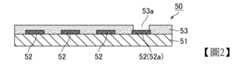
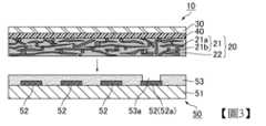
其次,說明使用了本發明第1實施形態之電磁波屏蔽膜的屏蔽印刷配線板之製造方法。 圖2為截面圖,其示意顯示屏蔽印刷配線板之製造方法的印刷配線板準備步驟,且該屏蔽印刷配線板之製造方法中使用了本發明第1實施形態之電磁波屏蔽膜。 圖3為截面圖,其示意顯示屏蔽印刷配線板之製造方法的電磁波屏蔽膜貼合步驟,且該屏蔽印刷配線板之製造方法中使用了本發明第1實施形態之電磁波屏蔽膜。 圖4為截面圖,其示意顯示屏蔽印刷配線板之製造方法的加熱加壓步驟,且該屏蔽印刷配線板之製造方法中使用了本發明第1實施形態之電磁波屏蔽膜。Next, a method for manufacturing a shielded printed wiring board using the electromagnetic wave shielding film of the first embodiment of the present invention is described.FIG. 2 is a cross-sectional view schematically showing a printed wiring board preparation step of the method for manufacturing a shielded printed wiring board, and the electromagnetic wave shielding film of the first embodiment of the present invention is used in the method for manufacturing a shielded printed wiring board.FIG. 3 is a cross-sectional view schematically showing an electromagnetic wave shielding film bonding step of the method for manufacturing a shielded printed wiring board, and the electromagnetic wave shielding film of the first embodiment of the present invention is used in the method for manufacturing a shielded printed wiring board.FIG. 4 is a cross-sectional view schematically showing a heating and pressurizing step of the method for manufacturing a shielded printed wiring board, and the electromagnetic wave shielding film of the first embodiment of the present invention is used in the method for manufacturing a shielded printed wiring board.
(1)印刷配線板準備步驟 首先,如圖2所示,準備印刷配線板50,該印刷配線板50具備基底膜51、配置於基底膜51上的印刷電路52及配置成覆蓋印刷電路52的覆蓋層53。(1) Printed wiring board preparation stepFirst, as shown in FIG. 2 , a printed
另,印刷配線板50中,印刷電路52包含接地電路52a,並於覆蓋層53形成有使接地電路52a露出之開口部53a。In the printed
基底膜51及覆蓋層53之材料並無特殊限制,宜由工程塑膠構成。此種工程塑膠可舉例如:聚對苯二甲酸乙二酯、聚丙烯、交聯聚乙烯、聚酯、聚苯并咪唑、聚醯亞胺、聚醯亞胺醯胺、聚醚醯亞胺、聚伸苯硫醚等樹脂。 又,該等工程塑膠中,當要求阻燃性時,宜為聚伸苯硫醚膜,當要求耐熱性時,則宜為聚醯亞胺膜。另,基底膜51之厚度宜為10~40μm。又,覆蓋層53之厚度宜為10~30μm。The materials of the
印刷電路52並無特殊限制,可藉由對導電材料進行蝕刻處理等來形成。 導電材料可列舉銅、鎳、銀、金等。The printed
(2)電磁波屏蔽膜貼合步驟 接著,如圖3所示,準備電磁波屏蔽膜10,將電磁波屏蔽膜10以其導電性接著劑層20與覆蓋層53相接之方式配置於印刷配線板50。(2) Electromagnetic wave shielding film bonding stepNext, as shown in FIG. 3 , an electromagnetic
(3)加熱加壓步驟 接著,如圖4所示,進行加熱加壓,使電磁波屏蔽膜10貼合於印刷配線板50。 加熱加壓之條件宜為150~200℃、2~5MPa、1~10min。(3) Heating and Pressurizing StepNext, as shown in FIG. 4 , heating and pressing are performed to adhere the electromagnetic
藉由加熱加壓步驟,導電性接著劑層20會填埋開口部53a。Through the heating and pressurizing steps, the conductive
經由以上步驟,可製得屏蔽印刷配線板60。Through the above steps, the shielded printed
另,屏蔽印刷配線板60亦為本發明之屏蔽印刷配線板之一例。In addition, the shielded printed
屏蔽印刷配線板60中,於電磁波屏蔽膜10之導電性接著劑層20中包含小片狀導電性粒子21a及球狀導電性粒子21b。 由於小片狀導電性粒子21a具有充分之柔軟性,因此,當反覆彎折屏蔽印刷配線板60時,小片狀導電性粒子21a亦可順應彎曲,小片狀導電性粒子21a之位置就不易偏離。其結果,可充分保持導電性粒子21彼此之接觸,並且可防止電阻值上升。 又,若含有球狀導電性粒子21b,球狀導電性粒子21b會被夾入導電性接著劑層20之厚度方向上的小片狀導電性粒子21a彼此之間,且於小片狀導電性粒子21a間存在許多接著性樹脂組成物。因此,導電性接著劑層20之機械強度提升,剝離強度會提高。 又,球狀導電性粒子21b會進入小片狀導電性粒子21a彼此之間,小片狀導電性粒子21a彼此可透過球狀導電性粒子21b而電連接。因此,導電性接著劑層20之屏蔽性提升。In the shielded printed
屏蔽印刷配線板60中,球狀導電性粒子21b之平均粒徑為1~10μm。 若球狀導電性粒子之平均粒徑小於1μm,球狀導電性粒子不易成為立體阻礙,小片狀導電性粒子便容易於導電性接著劑層之表面露出。其結果為導電性接著劑層之剝離強度降低。 若球狀導電性粒子之平均粒徑大於10μm,則導電性接著劑層之導電性降低,屏蔽性會降低。In the shielded printed
屏蔽印刷配線板60中,導電性接著劑層20中小片狀導電性粒子21a及球狀導電性粒子21b之含量為70~80wt%。 若導電性接著劑層中小片狀導電性粒子及球狀導電性粒子之含量小於70wt%,由於導電性粒子少,因此球狀導電性粒子變得不易夾入小片狀導電性粒子彼此之間。其結果就導致小片狀導電性粒子彼此不易透過球狀導電性粒子而電連接,電磁波屏蔽膜之屏蔽性會降低。 若導電性接著劑層中小片狀導電性粒子及球狀導電性粒子之含量大於80wt%,相對而言接著性樹脂組成物之含量會降低。由於導電性接著劑層之剝離強度依存於接著性樹脂組成物之含量,因此導電性接著劑層之剝離強度會降低。In the shielded printed
屏蔽印刷配線板60中,小片狀導電性粒子21a與球狀導電性粒子21b之重量比為[小片狀導電性粒子]/[球狀導電性粒子]=6/4~8/2。 若小片狀導電性粒子與球狀導電性粒子之重量比小於[小片狀導電性粒子]/[球狀導電性粒子]=6/4,則球狀導電性粒子之比例變得過多,小片狀導電性粒子之重疊面積減少,而且,於小片狀導電性粒子間存在許多球狀導電性粒子,因此小片狀導電性粒子間的間隔擴大,導電性(屏蔽性)降低。再者,予以撓曲時,也會使導電性粒子間的連接惡化。 若小片狀導電性粒子與球狀導電性粒子之重量比大於[小片狀導電性粒子]/[球狀導電性粒子]=8/2,雖然小片狀導電性粒子之重疊面積會擴大且屏蔽性能提升,但小片狀導電性粒子之間隔卻縮小,導電性接著劑層之剝離強度會降低,而成為從屏蔽印刷配線板剝落的原因。In the shielded printed
屏蔽印刷配線板60中,導電性接著劑層20之厚度為5~20μm,宜為8~15μm。 若導電性接著劑層之厚度小於5μm,為了確保高屏蔽性能,導電性粒子之填充量就要提高,而變得無法維持柔軟性及剝離強度。 若導電性接著劑層之厚度大於20μm,針對高屏蔽化的設計會變得容易,但電磁波屏蔽膜卻無法薄型化,屏蔽印刷配線板會變大。In the shielded printed
(第2實施形態) 其次,說明本發明第2實施形態之電磁波屏蔽膜。 圖5為截面圖,其示意顯示本發明第2實施形態之電磁波屏蔽膜之一例。 圖5所示電磁波屏蔽膜110其結構除了未配置有金屬層40外,其餘皆與上述本發明第1實施形態之電磁波屏蔽膜10相同。 即,電磁波屏蔽膜110是由導電性接著劑層20及積層於導電性接著劑層20上的絕緣層30構成,該導電性接著劑層20包含導電性粒子21及接著性樹脂組成物22,且該導電性粒子21包含小片狀導電性粒子21a及球狀導電性粒子21b。(Second embodiment)Next, the electromagnetic wave shielding film of the second embodiment of the present invention will be described.FIG. 5 is a cross-sectional view schematically showing an example of the electromagnetic wave shielding film of the second embodiment of the present invention.The structure of the electromagnetic
電磁波屏蔽膜110中導電性接著劑層20、小片狀導電性粒子21a及球狀導電性粒子21b、接著性樹脂組成物22及絕緣層30之理想結構,是與上述電磁波屏蔽膜110中導電性接著劑層20、小片狀導電性粒子21a及球狀導電性粒子21b、接著性樹脂組成物22及絕緣層30之理想結構相同。The ideal structure of the conductive
即便為此種結構,電磁波屏蔽膜110亦可薄型化且剝離強度強,而且導電性、屏蔽性以及對高低差的耐撓曲性及順應性高。Even with such a structure, the electromagnetic
實施例 以下顯示用以更具體說明本發明之實施例,惟本發明並非受限於該等實施例。EmbodimentsThe following are embodiments for more specifically illustrating the present invention, but the present invention is not limited to these embodiments.
(實施例1) 於轉印膜上塗敷環氧樹脂,並使用電烘箱,於100℃下加熱2分鐘,製作出厚度5μm之絕緣層。(Example 1)Epoxy resin was applied on the transfer film and heated in an electric oven at 100°C for 2 minutes to produce an insulating layer with a thickness of 5 μm.
接著,準備表1中記載的小片狀導電性粒子及球狀導電性粒子、以及接著性樹脂組成物(甲酚酚醛清漆型環氧樹脂:DIC公司製「EPICLON N-655-EXP」),將該等混合成表1中記載之摻合量,而製作出導電性樹脂組成物。另,小片狀導電性粒子粉及球狀導電性粒子之平均粒徑是使用麥奇克(Microtrac)公司製之MT3300EXII,利用雷射繞射散射式粒度分布測定法來測定。Next, the flake-shaped conductive particles and spherical conductive particles listed in Table 1 and an adhesive resin composition (cresol novolac type epoxy resin: "EPICLON N-655-EXP" manufactured by DIC Corporation) were prepared and mixed in the blending amounts listed in Table 1 to prepare a conductive resin composition. The average particle size of the flake-shaped conductive particle powder and the spherical conductive particles was measured by laser diffraction scattering particle size distribution measurement method using MT3300EXII manufactured by Microtrac Corporation.
接著,於絕緣層上塗佈導電性樹脂組成物,形成厚度15μm之導電性接著劑層,製得實施例1之電磁波屏蔽膜。Next, a conductive resin composition was coated on the insulating layer to form a conductive adhesive layer with a thickness of 15 μm, thereby obtaining the electromagnetic wave shielding film of Example 1.
(實施例2~9)及(比較例1~15) 除了將小片狀導電性粒子及球狀導電性粒子之種類、摻合比率及含量、以及導電性接著劑層之厚度設為如表1及表2所示之外,以與實施例1相同方式製得實施例2~9及比較例1~15之電磁波屏蔽膜。(Examples 2 to 9) and (Comparative Examples 1 to 15)Except that the types, blending ratios and contents of the flake-shaped conductive particles and the spherical conductive particles, and the thickness of the conductive adhesive layer are set as shown in Tables 1 and 2, the electromagnetic wave shielding films of Examples 2 to 9 and Comparative Examples 1 to 15 are prepared in the same manner as Example 1.
[表1][Table 1]
[表2][Table 2]
(加熱加壓試驗) 準備厚度25μm之聚醯亞胺樹脂板,並將各實施例及各比較例之電磁波屏蔽膜以其導電性接著劑層與該聚醯亞胺樹脂板相接之方式進行配置。 接著,於150℃、2MPa、30min之條件下加熱加壓,使各實施例及各比較例之電磁波屏蔽膜貼合於聚醯亞胺樹脂板。(Heating and Pressurizing Test)A polyimide resin plate with a thickness of 25 μm was prepared, and the electromagnetic wave shielding films of each embodiment and each comparative example were arranged in such a manner that their conductive adhesive layer was connected to the polyimide resin plate.Then, heating and pressurizing were performed under the conditions of 150°C, 2 MPa, and 30 min to bond the electromagnetic wave shielding films of each embodiment and each comparative example to the polyimide resin plate.
將加熱加壓試驗後的電磁波屏蔽膜切斷,拍攝SEM影像,並使用影像處理軟體(SEM Control User Interface Ver3.10),測定各導電性粒子之粒徑及縱橫比。於表1及表2中顯示結果。The electromagnetic wave shielding film after the heat and pressure test was cut, and SEM images were taken. The particle size and aspect ratio of each conductive particle were measured using image processing software (SEM Control User Interface Ver3.10). The results are shown in Tables 1 and 2.
又,從SEM影像測定小片狀導電性粒子間距離。於表1及表2中顯示結果。In addition, the distance between the flake-shaped conductive particles was measured from the SEM images. The results are shown in Tables 1 and 2.
顯示實施例1之電磁波屏蔽膜的截面SEM影像作為代表例。 圖6為實施例1之電磁波屏蔽膜的截面SEM影像。The cross-sectional SEM image of the electromagnetic wave shielding film of Example 1 is shown as a representative example.Figure 6 is a cross-sectional SEM image of the electromagnetic wave shielding film of Example 1.
又,另外在與上述加熱加壓條件相同之條件下,將各實施例及各比較例之電磁波屏蔽膜貼合於聚醯亞胺樹脂板,然後,測定從聚醯亞胺樹脂板剝離電磁波屏蔽膜時的剝離強度。於表1及表2中顯示結果。Furthermore, under the same heating and pressurizing conditions as described above, the electromagnetic wave shielding films of each example and each comparative example were bonded to a polyimide resin plate, and then the peeling strength when the electromagnetic wave shielding films were peeled off from the polyimide resin plate was measured. The results are shown in Tables 1 and 2.
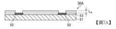
(連接電阻值測定試驗) 使用各實施例及各比較例之電磁波屏蔽膜,利用以下方法,測定各實施例及各比較例之電磁波屏蔽膜之電阻值。於表1及表2中顯示測定結果。 圖7A及圖7B為側視截面圖,其示意顯示連接電阻值測定試驗之方法。 如圖7A所示,準備一連接電阻值測定用印刷配線板50A,其係在基底膜51上形成有2個未相互連接的印刷電路52、並形成有覆蓋基底膜51及印刷電路52的覆蓋層53者。另,於覆蓋層53形成有可露出各印刷電路52之一部分的開口部53a,且所述開口部53a為直徑0.8mm、深度(圖7A中符號LA所示距離)27.5μm。(Connection resistance value measurement test) The electromagnetic wave shielding film of each embodiment and each comparative example was used to measure the resistance value of the electromagnetic wave shielding film of each embodiment and each comparative example by the following method. The measurement results are shown in Tables 1 and 2. FIG. 7A and FIG. 7B are side cross-sectional views, which schematically show the method of the connection resistance value measurement test. As shown in FIG. 7A, a printed
接著,如圖7B所示,以各實施例及各比較例之電磁波屏蔽膜110之導電性接著劑層20與覆蓋層53接觸之方式,將電磁波屏蔽膜110貼合於連接電阻值測定用印刷配線板50A,並利用壓機,於溫度:170℃、時間30分鐘、壓力3MPa之條件下進行壓接。藉此,導電性接著劑層20會進入開口部53a,導電性接著劑層20與印刷電路52接觸,印刷電路52彼此可透過導電性接著劑層20而電連接。 然後,利用電阻器70測定印刷電路52間的電阻值。Next, as shown in FIG. 7B , the electromagnetic
(屏蔽性之評價) 針對各實施例及各比較例之電磁波屏蔽膜之屏蔽性,利用KEC法進行評價;該KEC法是使用由一般社團法人KEC關西電子工業振興中心所開發的電磁波屏蔽效果測定裝置。 圖8為示意圖,其示意顯示KEC法中所用系統之構造。 KEC法中所用系統是由以下構成:電磁波屏蔽效果測定裝置80、頻譜分析儀91、進行10dB之衰減的衰減器92、進行3dB之衰減的衰減器93及前置放大器94。(Evaluation of shielding properties)The shielding properties of the electromagnetic wave shielding films of each embodiment and each comparative example were evaluated by the KEC method; the KEC method uses an electromagnetic wave shielding effect measuring device developed by the Kansai Electronic Industry Promotion Center KEC.Fig. 8 is a schematic diagram showing the structure of the system used in the KEC method.The system used in the KEC method is composed of the following: an electromagnetic wave shielding
如圖8所示,於電磁波屏蔽效果測定裝置80中,2個測定夾具83係呈對向設置。並且設置成可於該測定夾具83間夾持各實施例及各比較例之電磁波屏蔽膜(圖8中以符號110表示)。測定夾具83採用TEM室(橫向電磁室,Transverse Electro Magnetic Cell)之尺寸分配,並形成在與其傳輸軸方向呈垂直的面內以左右對稱之方式分割的構造。不過,為了防止因電磁波屏蔽膜110之插入而形成短路,平板狀的中心導體84係以在其與各測定夾具83間設置間隙之方式來配置。As shown in FIG8 , in the electromagnetic wave shielding
KEC法首先係透過衰減器92,將從頻譜分析儀91輸出的信號輸入至發送側的測定夾具83。然後,藉由前置放大器94,將業經接收側的測定夾具83接收且已經過衰減器93的信號擴大後,利用頻譜分析儀91測定信號位準。另,頻譜分析儀91是以未於電磁波屏蔽效果測定裝置80中設置電磁波屏蔽膜110的狀態為基準,輸出已於電磁波屏蔽效果測定裝置80中設置電磁波屏蔽膜110時的衰減量。The KEC method first inputs the signal output from the
使用此種裝置,於溫度25℃、相對濕度30~50%之條件下,將各實施例及各比較例之電磁波屏蔽膜裁切成15cm見方,並進行於200MHz下的屏蔽性測定。於表1及表2中顯示測定結果。Using this device, the electromagnetic wave shielding films of each embodiment and each comparative example were cut into 15 cm squares under the conditions of temperature 25°C and relative humidity 30-50%, and the shielding properties were measured at 200 MHz. The measurement results are shown in Tables 1 and 2.
(對高低差的耐撓曲性及順應性之評價) 使用各實施例及各比較例之電磁波屏蔽膜,利用以下方法,測定各實施例及各比較例之電磁波屏蔽膜對高低差的耐撓曲性及順應性。 圖9A及圖9B為側視截面圖,其示意顯示對高低差的耐撓曲性及順應性之評價中測定連接電阻值之方法。 首先,準備圖9A所示連接電阻值測定用印刷配線板150。 連接電阻值測定用印刷配線板150是由印刷配線板部151及形成於印刷配線板部151上的高低差形成部152構成。 印刷配線板部151是由基底膜151a、積層於基底膜151a上的下方銅層151b及形成於下方銅層151b上的覆蓋層151c構成。 下方銅層151b具有下方電磁波屏蔽膜配置部171a及下方端子連接部171b,並於覆蓋層151c形成有使該等下方電磁波屏蔽膜配置部171a及下方端子連接部171b露出之第1溝部151c1及第2溝部151c2。 即,下方電磁波屏蔽膜配置部171a藉由第1溝部151c1而露出,下方端子連接部171b則藉由第2溝部151c2而露出。 另,對下方端子連接部171b施以鎳-金鍍敷。 高低差形成部152是由接著劑層152d、形成於接著劑層152d上的高低差部形成用絕緣層152a及形成於高低差部形成用絕緣層152a上的上方銅層152b構成。 高低差形成部152是透過接著劑層152d配置於印刷配線板部151上,並且形成高低差160。又,對上方銅層152b施以鎳-金鍍敷。 上方銅層152b具有上方電磁波屏蔽膜配置部172a及上方端子連接部172b,且以使該等上方電磁波屏蔽膜配置部172a及上方端子連接部172b露出之方式於上方銅層152b上形成有抗蝕層153。(Evaluation of the resistance to bending and compliance to height difference) The electromagnetic wave shielding films of each embodiment and each comparative example are used to measure the resistance to bending and compliance to height difference of the electromagnetic wave shielding films of each embodiment and each comparative example using the following method. FIG. 9A and FIG. 9B are side cross-sectional views, which schematically show the method of measuring the connection resistance value in the evaluation of the resistance to bending and compliance to height difference. First, prepare a printed
連接電阻值測定用印刷配線板150中高低差之高度(圖9A中符號LB所示距離)為288μm。The height of the step in the printed
其次,如圖9B所示,以各實施例及各比較例之電磁波屏蔽膜110之導電性接著劑層20在高低差160側之方式,將電磁波屏蔽膜110貼合於連接電阻值測定用印刷配線板150,並利用壓機,於溫度:170℃、時間30分鐘、壓力3MPa之條件下進行壓接。 藉此,導電性接著劑層20與下方電磁波屏蔽膜配置部171a接觸,且導電性接著劑層20與上方電磁波屏蔽膜配置部172a接觸。結果,下方銅層151b與上方銅層152b就能透過導電性接著劑層20而電連接。 然後,將端子連接於下方端子連接部171b及上方端子連接部172b,並利用電阻器170測定電阻值。於表1及表2中顯示測定結果。Next, as shown in FIG. 9B , the electromagnetic
然後,觀察各電磁波屏蔽膜在高低差160上之外觀並進行評價。 評價基準如下。於表1及表2中顯示結果。 ○:未發生破裂及浮起。 ×:發生破裂及/或浮起。 另,所謂「破裂」,意指電磁波屏蔽膜之至少一部分因高低差160而斷裂的狀態。 又,所謂「浮起」,意指從配置於連接電阻值測定用印刷配線板150上的電磁波屏蔽膜之上方俯視時,因高低差160而形成的電磁波屏蔽膜斜面之寬度大於100μm的狀態。「浮起」是因為在電磁波屏蔽膜與連接電阻值測定用印刷配線板150間產生空隙所引起的現象。Then, the appearance of each electromagnetic wave shielding film on the
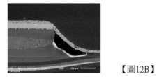
針對上述外觀評價,例示使用了實施例1、比較例5及比較例6之電磁波屏蔽膜時的照片。 圖10A為照片,係在對高低差的耐撓曲性及順應性之評價中,將實施例1之電磁波屏蔽膜壓接於連接電阻值測定用印刷配線板後,以從上方俯視之方式拍攝該電磁波屏蔽膜之高低差所得的照片。 圖10B為照片,係在對高低差的耐撓曲性及順應性之評價中,實施例1之電磁波屏蔽膜壓接於連接電阻值測定用印刷配線板後該電磁波屏蔽膜之高低差截面的照片。 圖11為照片,係在對高低差的耐撓曲性及順應性之評價中,將比較例5之電磁波屏蔽膜壓接於連接電阻值測定用印刷配線板後,以從上方俯視之方式拍攝該電磁波屏蔽膜之高低差所得的照片。 圖12A為照片,係在對高低差的耐撓曲性及順應性之評價中,將比較例6之電磁波屏蔽膜壓接於連接電阻值測定用印刷配線板後,以從上方俯視之方式拍攝該電磁波屏蔽膜之高低差所得的照片。 圖12B為照片,係在對高低差的耐撓曲性及順應性之評價中,比較例6之電磁波屏蔽膜壓接於連接電阻值測定用印刷配線板後該電磁波屏蔽膜之高低差截面的照片。For the above appearance evaluation, the photographs of the electromagnetic wave shielding films of Example 1, Comparative Example 5 and Comparative Example 6 are shown.FIG. 10A is a photograph of the electromagnetic wave shielding film of Example 1, which was pressed onto a printed wiring board for connecting resistance value measurement in the evaluation of the bending resistance and compliance to the height difference, and the height difference of the electromagnetic wave shielding film was photographed from above.FIG. 10B is a photograph of the height difference cross section of the electromagnetic wave shielding film of Example 1, which was pressed onto a printed wiring board for connecting resistance value measurement in the evaluation of the bending resistance and compliance to the height difference.FIG. 11 is a photograph obtained by pressing the electromagnetic wave shielding film of Comparative Example 5 onto a printed wiring board for measuring resistance value in the evaluation of the resistance to height difference and compliance, and then photographing the height difference of the electromagnetic wave shielding film from above.FIG. 12A is a photograph obtained by pressing the electromagnetic wave shielding film of Comparative Example 6 onto a printed wiring board for measuring resistance value in the evaluation of the resistance to height difference and compliance, and then photographing the height difference of the electromagnetic wave shielding film from above.FIG12B is a photograph of the cross section of the height difference of the electromagnetic wave shielding film after the electromagnetic wave shielding film of Comparative Example 6 is pressed onto the printed wiring board for connecting resistance value measurement in the evaluation of the bending resistance and compliance of the height difference.
如圖11所示,於上述外觀之觀察中,在比較例5之電磁波屏蔽膜發生了「破裂」。 如圖12A及圖12B所示,於上述外觀之觀察中,在比較例6之電磁波屏蔽膜發生了「浮起」。As shown in FIG. 11 , in the above-mentioned observation of the appearance, "cracks" occurred in the electromagnetic wave shielding film of Comparative Example 5.As shown in FIG. 12A and FIG. 12B , in the above-mentioned observation of the appearance, "lifting" occurred in the electromagnetic wave shielding film of Comparative Example 6.
如表1及表2所示,清楚明白本發明實施例之電磁波屏蔽膜可薄型化且剝離強度強,而且導電性、屏蔽性以及對高低差的耐撓曲性及順應性優異。As shown in Table 1 and Table 2, it is clear that the electromagnetic wave shielding film of the embodiment of the present invention can be thinned and has a strong peeling strength, and has excellent conductivity, shielding properties, and resistance to bending and compliance to height differences.
10,110:電磁波屏蔽膜 20:導電性接著劑層 21:導電性粒子 21a:小片狀導電性粒子 21b:球狀導電性粒子 22:接著性樹脂組成物 30:絕緣層 40:金屬層 50:印刷配線板 50A,150:連接電阻值測定用印刷配線板 51,151a:基底膜 52:印刷電路 52a:接地電路 53,151c:覆蓋層 53a:開口部 60:屏蔽印刷配線板 70,170:電阻器 80:電磁波屏蔽效果測定裝置 83:測定夾具 84:中心導體 91:頻譜分析儀 92,93:衰減器 94:前置放大器 151:印刷配線板部 151b:下方銅層 151c1:第1溝部 151c2:第2溝部 152:高低差形成部 152a:高低差部形成用絕緣層 152b:上方銅層 152d:接著劑層 153:抗蝕層 160:高低差 171a:下方電磁波屏蔽膜配置部 171b:下方端子連接部 172a:上方電磁波屏蔽膜配置部 172b:上方端子連接部 LA:開口部深度 LB:高低差之高度10,110: electromagnetic wave shielding film 20: conductive adhesive layer 21:
圖1為截面圖,其示意顯示本發明第1實施形態之電磁波屏蔽膜之一例。 圖2為截面圖,其示意顯示屏蔽印刷配線板之製造方法的印刷配線板準備步驟,且該屏蔽印刷配線板之製造方法中使用了本發明第1實施形態之電磁波屏蔽膜。 圖3為截面圖,其示意顯示屏蔽印刷配線板之製造方法的電磁波屏蔽膜貼合步驟,且該屏蔽印刷配線板之製造方法中使用了本發明第1實施形態之電磁波屏蔽膜。 圖4為截面圖,其示意顯示屏蔽印刷配線板之製造方法的加熱加壓步驟,且該屏蔽印刷配線板之製造方法中使用了本發明第1實施形態之電磁波屏蔽膜。 圖5為截面圖,其示意顯示本發明第2實施形態之電磁波屏蔽膜之一例。 圖6為實施例1之電磁波屏蔽膜的截面SEM影像。 圖7A為側視截面圖,其示意顯示連接電阻值測定試驗之方法。 圖7B為側視截面圖,其示意顯示連接電阻值測定試驗之方法。 圖8為示意圖,其示意顯示KEC法中所用系統之構造。 圖9A為側視截面圖,其示意顯示對高低差的耐撓曲性及順應性之評價中測定連接電阻值之方法。 圖9B為側視截面圖,其示意顯示對高低差的耐撓曲性及順應性之評價中測定連接電阻值之方法。 圖10A為照片,係在對高低差的耐撓曲性及順應性之評價中,將實施例1之電磁波屏蔽膜壓接於連接電阻值測定用印刷配線板後,以從上方俯視之方式拍攝該電磁波屏蔽膜之高低差所得的照片。 圖10B為照片,係在對高低差的耐撓曲性及順應性之評價中,實施例1之電磁波屏蔽膜壓接於連接電阻值測定用印刷配線板後該電磁波屏蔽膜之高低差截面的照片。 圖11為照片,係在對高低差的耐撓曲性及順應性之評價中,將比較例5之電磁波屏蔽膜壓接於連接電阻值測定用印刷配線板後,以從上方俯視之方式拍攝該電磁波屏蔽膜之高低差所得的照片。 圖12A為照片,係在對高低差的耐撓曲性及順應性之評價中,將比較例6之電磁波屏蔽膜壓接於連接電阻值測定用印刷配線板後,以從上方俯視之方式拍攝該電磁波屏蔽膜之高低差所得的照片。 圖12B為照片,係在對高低差的耐撓曲性及順應性之評價中,比較例6之電磁波屏蔽膜壓接於連接電阻值測定用印刷配線板後該電磁波屏蔽膜之高低差截面的照片。FIG. 1 is a cross-sectional view schematically showing an example of an electromagnetic wave shielding film of the first embodiment of the present invention.FIG. 2 is a cross-sectional view schematically showing a printed wiring board preparation step of a method for manufacturing a shielded printed wiring board, and the electromagnetic wave shielding film of the first embodiment of the present invention is used in the method for manufacturing a shielded printed wiring board.FIG. 3 is a cross-sectional view schematically showing an electromagnetic wave shielding film bonding step of a method for manufacturing a shielded printed wiring board, and the electromagnetic wave shielding film of the first embodiment of the present invention is used in the method for manufacturing a shielded printed wiring board.FIG. 4 is a cross-sectional view schematically showing a heating and pressurizing step of a method for manufacturing a shielded printed wiring board, and the electromagnetic wave shielding film of the first embodiment of the present invention is used in the method for manufacturing a shielded printed wiring board.FIG. 5 is a cross-sectional view schematically showing an example of an electromagnetic wave shielding film of the second embodiment of the present invention.FIG. 6 is a cross-sectional SEM image of the electromagnetic wave shielding film of Example 1.FIG. 7A is a side cross-sectional view schematically showing a method for measuring a connection resistance value test.FIG. 7B is a side cross-sectional view schematically showing a method for measuring a connection resistance value test.FIG. 8 is a schematic diagram schematically showing the structure of a system used in the KEC method.FIG. 9A is a side cross-sectional view schematically showing a method for measuring a connection resistance value in the evaluation of the bending resistance and compliance to the height difference.FIG. 9B is a side cross-sectional view schematically showing a method for measuring a connection resistance value in the evaluation of the bending resistance and compliance to the height difference.FIG. 10A is a photograph of the height difference of the electromagnetic wave shielding film of Example 1 after it is pressed onto a printed wiring board for measuring resistance value in the evaluation of the resistance to height difference and compliance.FIG. 10B is a photograph of the height difference cross section of the electromagnetic wave shielding film of Example 1 after it is pressed onto a printed wiring board for measuring resistance value in the evaluation of the resistance to height difference and compliance.FIG. 11 is a photograph obtained by pressing the electromagnetic wave shielding film of Comparative Example 5 onto a printed wiring board for measuring resistance value in the evaluation of the resistance to height difference and compliance, and then photographing the height difference of the electromagnetic wave shielding film from above.FIG. 12A is a photograph obtained by pressing the electromagnetic wave shielding film of Comparative Example 6 onto a printed wiring board for measuring resistance value in the evaluation of the resistance to height difference and compliance, and then photographing the height difference of the electromagnetic wave shielding film from above.FIG12B is a photograph of the cross section of the height difference of the electromagnetic wave shielding film after the electromagnetic wave shielding film of Comparative Example 6 is pressed onto the printed wiring board for connecting resistance value measurement in the evaluation of the bending resistance and compliance of the height difference.
Claims (7)
Translated fromChineseApplications Claiming Priority (2)
| Application Number | Priority Date | Filing Date | Title |
|---|---|---|---|
| JP2020-158576 | 2020-09-23 | ||
| JP2020158576 | 2020-09-23 |
Publications (2)
| Publication Number | Publication Date |
|---|---|
| TW202219215A TW202219215A (en) | 2022-05-16 |
| TWI847061Btrue TWI847061B (en) | 2024-07-01 |
Family
ID=80846564
Family Applications (1)
| Application Number | Title | Priority Date | Filing Date |
|---|---|---|---|
| TW110135365ATWI847061B (en) | 2020-09-23 | 2021-09-23 | Electromagnetic wave shielding film and shielding printed wiring board |
Country Status (6)
| Country | Link |
|---|---|
| US (1) | US12120861B2 (en) |
| JP (2) | JP7463523B2 (en) |
| KR (1) | KR102861085B1 (en) |
| CN (1) | CN116096561A (en) |
| TW (1) | TWI847061B (en) |
| WO (1) | WO2022065380A1 (en) |
Families Citing this family (3)
| Publication number | Priority date | Publication date | Assignee | Title |
|---|---|---|---|---|
| TW202316949A (en)* | 2021-09-30 | 2023-04-16 | 日商拓自達電線股份有限公司 | Electromagnetic wave shielding film and shielded printed wiring board |
| CN115696898B (en)* | 2022-11-08 | 2025-08-19 | 广州方邦电子股份有限公司 | Electromagnetic shielding film and circuit board |
| CN117395977B (en)* | 2023-11-20 | 2024-03-22 | 广州方邦电子股份有限公司 | Electromagnetic shielding film and application thereof |
Citations (2)
| Publication number | Priority date | Publication date | Assignee | Title |
|---|---|---|---|---|
| JP2016076444A (en)* | 2014-10-08 | 2016-05-12 | 化研テック株式会社 | Conductive paste and electromagnetic wave shielding member |
| JP2018060987A (en)* | 2016-01-21 | 2018-04-12 | 東洋インキScホールディングス株式会社 | Electromagnetic wave shielding sheet and printed wiring board |
Family Cites Families (9)
| Publication number | Priority date | Publication date | Assignee | Title |
|---|---|---|---|---|
| JP5609064B2 (en) | 2009-11-02 | 2014-10-22 | 住友電気工業株式会社 | Shielded flat cable and manufacturing method thereof |
| JP2012067327A (en) | 2010-09-21 | 2012-04-05 | Mitsui Mining & Smelting Co Ltd | Copper powder for conductive paste, and conductive paste |
| JP2012248399A (en) | 2011-05-27 | 2012-12-13 | Tokai Rubber Ind Ltd | Soft conductive material and method for producing the same |
| JP2013008810A (en) | 2011-06-24 | 2013-01-10 | Sumitomo Electric Ind Ltd | Method of manufacturing printed wiring board, and printed wiring board |
| JP5598739B2 (en) | 2012-05-18 | 2014-10-01 | 株式会社マテリアル・コンセプト | Conductive paste |
| JP6127943B2 (en) | 2013-12-02 | 2017-05-17 | 住友金属鉱山株式会社 | Aqueous silver colloidal liquid, method for producing the same, and paint using aqueous silver colloidal liquid |
| JP6028290B2 (en) | 2014-12-11 | 2016-11-16 | 東洋インキScホールディングス株式会社 | Electromagnetic shielding sheet and printed wiring board |
| JP6318137B2 (en) | 2015-09-30 | 2018-04-25 | Dowaエレクトロニクス株式会社 | Conductive paste and conductive film |
| JP7363103B2 (en)* | 2019-05-30 | 2023-10-18 | 東洋インキScホールディングス株式会社 | Electromagnetic shielding sheets and printed wiring boards |
- 2021
- 2021-09-22WOPCT/JP2021/034857patent/WO2022065380A1/ennot_activeCeased
- 2021-09-22CNCN202180062599.XApatent/CN116096561A/enactivePending
- 2021-09-22JPJP2022540625Apatent/JP7463523B2/enactiveActive
- 2021-09-22USUS18/044,529patent/US12120861B2/enactiveActive
- 2021-09-22KRKR1020237005943Apatent/KR102861085B1/enactiveActive
- 2021-09-23TWTW110135365Apatent/TWI847061B/enactive
- 2023
- 2023-06-05JPJP2023092391Apatent/JP2023120233A/ennot_activeWithdrawn
Patent Citations (2)
| Publication number | Priority date | Publication date | Assignee | Title |
|---|---|---|---|---|
| JP2016076444A (en)* | 2014-10-08 | 2016-05-12 | 化研テック株式会社 | Conductive paste and electromagnetic wave shielding member |
| JP2018060987A (en)* | 2016-01-21 | 2018-04-12 | 東洋インキScホールディングス株式会社 | Electromagnetic wave shielding sheet and printed wiring board |
Also Published As
| Publication number | Publication date |
|---|---|
| JP7463523B2 (en) | 2024-04-08 |
| KR20230070200A (en) | 2023-05-22 |
| JPWO2022065380A1 (en) | 2022-03-31 |
| JP2023120233A (en) | 2023-08-29 |
| WO2022065380A1 (en) | 2022-03-31 |
| US20230337408A1 (en) | 2023-10-19 |
| US12120861B2 (en) | 2024-10-15 |
| CN116096561A (en) | 2023-05-09 |
| TW202219215A (en) | 2022-05-16 |
| KR102861085B1 (en) | 2025-09-16 |
Similar Documents
| Publication | Publication Date | Title |
|---|---|---|
| TWI847061B (en) | Electromagnetic wave shielding film and shielding printed wiring board | |
| TWI700984B (en) | Shielding film for printed wiring board and printed wiring board | |
| JP6857288B1 (en) | Electromagnetic wave shield film and shield printed wiring board | |
| TWI761781B (en) | Grounding member, shielded printed wiring board, and manufacturing method of shielded printed wiring board | |
| TW201841742A (en) | Shield film, shielded printed circuit board, and method for manufacturing shielded printed circuit board | |
| CN112586103B (en) | Electromagnetic wave shielding film, method for manufacturing shielding printed wiring board, and shielding printed wiring board | |
| CN112534974B (en) | Electromagnetic wave shielding film, method for manufacturing shielding printed wiring board, and shielding printed wiring board | |
| KR102640159B1 (en) | Shielded printed wiring board and manufacturing method of shielded printed wiring board | |
| TW202316949A (en) | Electromagnetic wave shielding film and shielded printed wiring board | |
| TWI854159B (en) | Electromagnetic wave shielding film and shielding printed wiring board | |
| TW202312855A (en) | Electromagnetic-wave-shielding film | |
| CN118901288A (en) | Conductive adhesive layer and heat dissipation structure | |
| CN118140606A (en) | Electromagnetic wave shielding film | |
| HK40050210A (en) | Shield printed wiring board and method of manufacturing shield printed wiring board |