TWI846591B - Bonding device and bonding method - Google Patents
Bonding device and bonding methodDownload PDFInfo
- Publication number
- TWI846591B TWI846591BTW112134471ATW112134471ATWI846591BTW I846591 BTWI846591 BTW I846591BTW 112134471 ATW112134471 ATW 112134471ATW 112134471 ATW112134471 ATW 112134471ATW I846591 BTWI846591 BTW I846591B
- Authority
- TW
- Taiwan
- Prior art keywords
- substrate
- adsorption
- bonding
- wafer
- area
- Prior art date
Links
Images


Classifications
- H—ELECTRICITY
- H01—ELECTRIC ELEMENTS
- H01L—SEMICONDUCTOR DEVICES NOT COVERED BY CLASS H10
- H01L21/00—Processes or apparatus adapted for the manufacture or treatment of semiconductor or solid state devices or of parts thereof
- H01L21/67—Apparatus specially adapted for handling semiconductor or electric solid state devices during manufacture or treatment thereof; Apparatus specially adapted for handling wafers during manufacture or treatment of semiconductor or electric solid state devices or components ; Apparatus not specifically provided for elsewhere
- H01L21/67005—Apparatus not specifically provided for elsewhere
- H01L21/67011—Apparatus for manufacture or treatment
- H01L21/67092—Apparatus for mechanical treatment
- B—PERFORMING OPERATIONS; TRANSPORTING
- B23—MACHINE TOOLS; METAL-WORKING NOT OTHERWISE PROVIDED FOR
- B23K—SOLDERING OR UNSOLDERING; WELDING; CLADDING OR PLATING BY SOLDERING OR WELDING; CUTTING BY APPLYING HEAT LOCALLY, e.g. FLAME CUTTING; WORKING BY LASER BEAM
- B23K20/00—Non-electric welding by applying impact or other pressure, with or without the application of heat, e.g. cladding or plating
- B—PERFORMING OPERATIONS; TRANSPORTING
- B32—LAYERED PRODUCTS
- B32B—LAYERED PRODUCTS, i.e. PRODUCTS BUILT-UP OF STRATA OF FLAT OR NON-FLAT, e.g. CELLULAR OR HONEYCOMB, FORM
- B32B38/00—Ancillary operations in connection with laminating processes
- B32B38/18—Handling of layers or the laminate
- B32B38/1858—Handling of layers or the laminate using vacuum
- H—ELECTRICITY
- H01—ELECTRIC ELEMENTS
- H01L—SEMICONDUCTOR DEVICES NOT COVERED BY CLASS H10
- H01L21/00—Processes or apparatus adapted for the manufacture or treatment of semiconductor or solid state devices or of parts thereof
- H01L21/02—Manufacture or treatment of semiconductor devices or of parts thereof
- H01L21/04—Manufacture or treatment of semiconductor devices or of parts thereof the devices having potential barriers, e.g. a PN junction, depletion layer or carrier concentration layer
- H01L21/18—Manufacture or treatment of semiconductor devices or of parts thereof the devices having potential barriers, e.g. a PN junction, depletion layer or carrier concentration layer the devices having semiconductor bodies comprising elements of Group IV of the Periodic Table or AIIIBV compounds with or without impurities, e.g. doping materials
- H01L21/185—Joining of semiconductor bodies for junction formation
- H01L21/187—Joining of semiconductor bodies for junction formation by direct bonding
- H—ELECTRICITY
- H01—ELECTRIC ELEMENTS
- H01L—SEMICONDUCTOR DEVICES NOT COVERED BY CLASS H10
- H01L21/00—Processes or apparatus adapted for the manufacture or treatment of semiconductor or solid state devices or of parts thereof
- H01L21/67—Apparatus specially adapted for handling semiconductor or electric solid state devices during manufacture or treatment thereof; Apparatus specially adapted for handling wafers during manufacture or treatment of semiconductor or electric solid state devices or components ; Apparatus not specifically provided for elsewhere
- H01L21/67005—Apparatus not specifically provided for elsewhere
- H01L21/67242—Apparatus for monitoring, sorting or marking
- H01L21/67253—Process monitoring, e.g. flow or thickness monitoring
- H—ELECTRICITY
- H01—ELECTRIC ELEMENTS
- H01L—SEMICONDUCTOR DEVICES NOT COVERED BY CLASS H10
- H01L21/00—Processes or apparatus adapted for the manufacture or treatment of semiconductor or solid state devices or of parts thereof
- H01L21/67—Apparatus specially adapted for handling semiconductor or electric solid state devices during manufacture or treatment thereof; Apparatus specially adapted for handling wafers during manufacture or treatment of semiconductor or electric solid state devices or components ; Apparatus not specifically provided for elsewhere
- H01L21/68—Apparatus specially adapted for handling semiconductor or electric solid state devices during manufacture or treatment thereof; Apparatus specially adapted for handling wafers during manufacture or treatment of semiconductor or electric solid state devices or components ; Apparatus not specifically provided for elsewhere for positioning, orientation or alignment
- H—ELECTRICITY
- H01—ELECTRIC ELEMENTS
- H01L—SEMICONDUCTOR DEVICES NOT COVERED BY CLASS H10
- H01L21/00—Processes or apparatus adapted for the manufacture or treatment of semiconductor or solid state devices or of parts thereof
- H01L21/67—Apparatus specially adapted for handling semiconductor or electric solid state devices during manufacture or treatment thereof; Apparatus specially adapted for handling wafers during manufacture or treatment of semiconductor or electric solid state devices or components ; Apparatus not specifically provided for elsewhere
- H01L21/683—Apparatus specially adapted for handling semiconductor or electric solid state devices during manufacture or treatment thereof; Apparatus specially adapted for handling wafers during manufacture or treatment of semiconductor or electric solid state devices or components ; Apparatus not specifically provided for elsewhere for supporting or gripping
- H01L21/6838—Apparatus specially adapted for handling semiconductor or electric solid state devices during manufacture or treatment thereof; Apparatus specially adapted for handling wafers during manufacture or treatment of semiconductor or electric solid state devices or components ; Apparatus not specifically provided for elsewhere for supporting or gripping with gripping and holding devices using a vacuum; Bernoulli devices
- H—ELECTRICITY
- H01—ELECTRIC ELEMENTS
- H01L—SEMICONDUCTOR DEVICES NOT COVERED BY CLASS H10
- H01L21/00—Processes or apparatus adapted for the manufacture or treatment of semiconductor or solid state devices or of parts thereof
- H01L21/67—Apparatus specially adapted for handling semiconductor or electric solid state devices during manufacture or treatment thereof; Apparatus specially adapted for handling wafers during manufacture or treatment of semiconductor or electric solid state devices or components ; Apparatus not specifically provided for elsewhere
- H01L21/683—Apparatus specially adapted for handling semiconductor or electric solid state devices during manufacture or treatment thereof; Apparatus specially adapted for handling wafers during manufacture or treatment of semiconductor or electric solid state devices or components ; Apparatus not specifically provided for elsewhere for supporting or gripping
- H01L21/687—Apparatus specially adapted for handling semiconductor or electric solid state devices during manufacture or treatment thereof; Apparatus specially adapted for handling wafers during manufacture or treatment of semiconductor or electric solid state devices or components ; Apparatus not specifically provided for elsewhere for supporting or gripping using mechanical means, e.g. chucks, clamps or pinches
- H01L21/68714—Apparatus specially adapted for handling semiconductor or electric solid state devices during manufacture or treatment thereof; Apparatus specially adapted for handling wafers during manufacture or treatment of semiconductor or electric solid state devices or components ; Apparatus not specifically provided for elsewhere for supporting or gripping using mechanical means, e.g. chucks, clamps or pinches the wafers being placed on a susceptor, stage or support
- H01L21/68742—Apparatus specially adapted for handling semiconductor or electric solid state devices during manufacture or treatment thereof; Apparatus specially adapted for handling wafers during manufacture or treatment of semiconductor or electric solid state devices or components ; Apparatus not specifically provided for elsewhere for supporting or gripping using mechanical means, e.g. chucks, clamps or pinches the wafers being placed on a susceptor, stage or support characterised by a lifting arrangement, e.g. lift pins
- H—ELECTRICITY
- H01—ELECTRIC ELEMENTS
- H01L—SEMICONDUCTOR DEVICES NOT COVERED BY CLASS H10
- H01L21/00—Processes or apparatus adapted for the manufacture or treatment of semiconductor or solid state devices or of parts thereof
- H01L21/67—Apparatus specially adapted for handling semiconductor or electric solid state devices during manufacture or treatment thereof; Apparatus specially adapted for handling wafers during manufacture or treatment of semiconductor or electric solid state devices or components ; Apparatus not specifically provided for elsewhere
- H01L21/683—Apparatus specially adapted for handling semiconductor or electric solid state devices during manufacture or treatment thereof; Apparatus specially adapted for handling wafers during manufacture or treatment of semiconductor or electric solid state devices or components ; Apparatus not specifically provided for elsewhere for supporting or gripping
- H01L21/687—Apparatus specially adapted for handling semiconductor or electric solid state devices during manufacture or treatment thereof; Apparatus specially adapted for handling wafers during manufacture or treatment of semiconductor or electric solid state devices or components ; Apparatus not specifically provided for elsewhere for supporting or gripping using mechanical means, e.g. chucks, clamps or pinches
- H01L21/68714—Apparatus specially adapted for handling semiconductor or electric solid state devices during manufacture or treatment thereof; Apparatus specially adapted for handling wafers during manufacture or treatment of semiconductor or electric solid state devices or components ; Apparatus not specifically provided for elsewhere for supporting or gripping using mechanical means, e.g. chucks, clamps or pinches the wafers being placed on a susceptor, stage or support
- H01L21/6875—Apparatus specially adapted for handling semiconductor or electric solid state devices during manufacture or treatment thereof; Apparatus specially adapted for handling wafers during manufacture or treatment of semiconductor or electric solid state devices or components ; Apparatus not specifically provided for elsewhere for supporting or gripping using mechanical means, e.g. chucks, clamps or pinches the wafers being placed on a susceptor, stage or support characterised by a plurality of individual support members, e.g. support posts or protrusions
- B—PERFORMING OPERATIONS; TRANSPORTING
- B32—LAYERED PRODUCTS
- B32B—LAYERED PRODUCTS, i.e. PRODUCTS BUILT-UP OF STRATA OF FLAT OR NON-FLAT, e.g. CELLULAR OR HONEYCOMB, FORM
- B32B2457/00—Electrical equipment
- B32B2457/14—Semiconductor wafers
Landscapes
- Engineering & Computer Science (AREA)
- Physics & Mathematics (AREA)
- Condensed Matter Physics & Semiconductors (AREA)
- General Physics & Mathematics (AREA)
- Manufacturing & Machinery (AREA)
- Computer Hardware Design (AREA)
- Microelectronics & Electronic Packaging (AREA)
- Power Engineering (AREA)
- Mechanical Engineering (AREA)
- Container, Conveyance, Adherence, Positioning, Of Wafer (AREA)
- Pressure Welding/Diffusion-Bonding (AREA)
Abstract
Translated fromChineseDescription
Translated fromChinese本發明係關於接合裝置及接合方法。The present invention relates to a bonding device and a bonding method.
記載於專利文獻1之接合裝置具備從上方吸附上側基板之上夾盤,和從下方吸附下側基板之下夾盤,將兩片基板面對面後予以接合。具體而言,接合裝置首先下壓被吸附於上夾盤之基板的中心部,使與被吸附於下夾盤之基板的中央部接觸。依此,兩片基板之中心部彼此藉由分子間力等被接合。接著,接合裝置係將兩片基板被接合的接合區域從中心部擴展至外周部。 [先前技術文獻] [專利文獻]The bonding device described in
[專利文獻1]日本特開2015-095579號公報[Patent Document 1] Japanese Patent Application Publication No. 2015-095579
[發明所欲解決之課題][The problem that the invention wants to solve]
接合裝置等之基板處理裝置具有吸附保持基板之保持部。但是,以往之保持部係均勻地吸附被吸附於吸附面之基板,無法控制被吸附於吸附面之基板的歪斜。A substrate processing device such as a bonding device has a holding portion for adsorbing and holding a substrate. However, the conventional holding portion uniformly adsorbs the substrate adsorbed on the adsorption surface, and cannot control the skewness of the substrate adsorbed on the adsorption surface.
實施型態之一態樣的主要目的在於控制被吸附於吸附面之基板的歪斜。 [用以解決課題之手段]The main purpose of one embodiment is to control the deflection of the substrate adsorbed on the adsorption surface.[Means for solving the problem]
實施型態之一態樣的接合裝置,具備:保持部,其係在吸附基板之吸附面,具有吸附上述基板之吸附壓力被獨立控制的複數區域;複數吸附壓力產生部,其係使構成上述吸附面之複數上述區域之各者獨立產生吸附壓力;複數吸附壓力調整部,其係獨立調整藉由複數上述吸附壓力產生部之各者而產生的吸附壓力;對向保持部,其係與上述保持部對向配置,保持被接合於上述基板之與上述基板不同的第2基板;推壓部,其係將被保持於上述對向保持部之上述第2基板之中心部推壓至上述基板之中心;及控制部,其係控制複數上述吸附壓力產生部、複數上述吸附壓力調整部及上述推壓部,上述保持部具包含區劃複數上述區域的肋部,在上述吸附面之徑向中心,配置藉由一上述吸附壓力調整部調整上述吸附壓力的圓狀之上述區域,在上述圓狀之上述區域之徑向外側,於上述吸附面之圓周方向交替重複配置藉由一上述吸附壓力調整部調整上述吸附壓力的圓弧狀之上述區域,和藉由另外的上述吸附壓力調整部而調整上述吸附壓力的另外的圓弧狀之上述區域,分別以90°周期各配置4個,形成環狀區域,上述控制部係藉由以上述推壓部使上述第2基板之中心部接觸於上述基板之中心部,接著,在使上述第2基板之接合面和上述基板之接合面以全面接合之期間,將上述基板吸附於上述吸附面,並且在上述環狀區域之相鄰的兩個圓弧狀之上述區域產生不同的上述吸附壓力,依此控制在上述基板產生的歪斜。 [發明之效果]A bonding device according to one embodiment of the present invention comprises: a holding portion having a plurality of regions on a suction surface of a suction substrate, wherein the suction pressure of the suction substrate is independently controlled; a plurality of suction pressure generating portions, which enable each of the plurality of regions constituting the suction surface to independently generate suction pressure; a plurality of suction pressure adjusting portions, which independently adjust the suction pressure generated by each of the plurality of suction pressure generating portions; and a counter holding portion, which The holding portion is arranged opposite to the holding portion, and holds a second substrate different from the above substrate and bonded to the above substrate; a pressing portion, which presses the center of the second substrate held by the opposing holding portion to the center of the above substrate; and a control portion, which controls the plurality of adsorption pressure generating portions, the plurality of adsorption pressure adjusting portions, and the pressing portion, wherein the holding portion includes a rib portion dividing the plurality of the above regions, and in the radial direction of the above adsorption surface The above-mentioned circular area for adjusting the above-mentioned adsorption pressure by one of the above-mentioned adsorption pressure adjusting parts is arranged at the center, and the above-mentioned circular area for adjusting the above-mentioned adsorption pressure by one of the above-mentioned adsorption pressure adjusting parts and the above-mentioned other circular area for adjusting the above-mentioned adsorption pressure by another above-mentioned adsorption pressure adjusting part are alternately and repeatedly arranged in the circumferential direction of the above-mentioned adsorption surface, and the above-mentioned circular area for adjusting the above-mentioned adsorption pressure by another above-mentioned adsorption pressure adjusting part are arranged respectively at a period of 90 degrees. 4, forming an annular area, the control unit makes the center of the second substrate contact the center of the substrate by the pushing unit, and then, during the period of making the bonding surface of the second substrate and the bonding surface of the substrate fully bonded, the substrate is adsorbed on the adsorption surface, and different adsorption pressures are generated in the two adjacent arc-shaped areas of the annular area, thereby controlling the skew generated in the substrate.[Effect of the invention]
若藉由實施型態之一態樣時,可以控制被吸附於吸附面之基板的歪斜。By using one aspect of the implementation form, the deflection of the substrate adsorbed on the adsorption surface can be controlled.
以下,針對用以實施本發明之型態,參照圖面予以說明。在各圖面中,對於相同或對應之構成,賦予相同或對應的符號,省略說明。在以下之說明中,X軸方向、Y軸方向、Z軸方向為互相垂直的方向,X軸方向及Y軸方向為水平方向,Z軸方向為垂直方向。也將以垂直軸為旋轉中心的旋轉方向稱為θ方向。在本說明書中,下方係指垂直下方,上方係指垂直上方。Hereinafter, the form for implementing the present invention will be described with reference to the drawings. In each drawing, the same or corresponding symbols are given to the same or corresponding components, and the description is omitted. In the following description, the X-axis direction, the Y-axis direction, and the Z-axis direction are mutually perpendicular directions, the X-axis direction and the Y-axis direction are horizontal directions, and the Z-axis direction is a vertical direction. The rotation direction with the vertical axis as the rotation center is also called the θ direction. In this specification, the bottom refers to the vertical bottom, and the top refers to the vertical top.
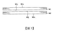
[接合系統] 圖1為表示與一實施型態有關之接合系統的俯視圖。圖2為表示與一實施型態有關之接合系統的側視圖。圖3為表示與一實施型態有關之第1基板及第2基板之接合前之狀態的側視圖。圖1所示之接合系統1藉由接合第1基板W1和第2基板W2形成重合基板T(參照圖7(b))。[Joining system]FIG. 1 is a top view of a joining system related to an embodiment. FIG. 2 is a side view of a joining system related to an embodiment. FIG. 3 is a side view of a state before joining of a first substrate and a second substrate related to an embodiment. The joining
第1基板W1係在例如矽晶圓或化合物半導體晶圓等之半導體基板形成複數電子電路的基板。再者,第2基板W2係無形成例如電子電路的裸晶圓。第1基板W1和第2基板W2具有略同徑。另外,即使在第2基板W2 形成電子電路亦可。The first substrate W1 is a substrate on which a plurality of electronic circuits are formed on a semiconductor substrate such as a silicon wafer or a compound semiconductor wafer. Furthermore, the second substrate W2 is a bare wafer on which no electronic circuits are formed. The first substrate W1 and the second substrate W2 have substantially the same diameter. In addition, it is also possible to form electronic circuits on the second substrate W2.
在以下中,有將第1基板W1記載為「上晶圓W1」,將第2基板W2記載為「下晶圓W2」,將重合基板T記載為「重合晶圓T」之情況。再者,在以下中,如圖3所示般,將上述晶圓W1之板面之中,將與下晶圓W2接合之側的板面,記載為「接合面W1j」,將與接合面W1j相反側之板面記載為「非接合面W1n」。再者,在以下中,將下晶圓W2之板面之中,將與上晶圓W1接合之側的板面,記載為「接合面W2j」,將與接合面W2j相反側之板面記載為「非接合面W2n」。In the following, the first substrate W1 is recorded as "upper wafer W1", the second substrate W2 is recorded as "lower wafer W2", and the overlapping substrate T is recorded as "overlapping wafer T". Furthermore, in the following, as shown in FIG. 3, among the plate surfaces of the above-mentioned wafer W1, the plate surface on the side to be bonded to the lower wafer W2 is recorded as "bonding surface W1j", and the plate surface on the opposite side to the bonding surface W1j is recorded as "non-bonding surface W1n". Furthermore, in the following, among the plate surfaces of the lower wafer W2, the plate surface on the side to be bonded to the upper wafer W1 is recorded as "bonding surface W2j", and the plate surface on the opposite side to the bonding surface W2j is recorded as "non-bonding surface W2n".
如圖1所示般,接合系統1具備搬入搬出站2和處理站3。搬入搬出站2及處理站3係沿著X軸正方向,以搬入搬出站2及處理站3之順序被排列配置。再者,搬入搬出站2及處理站3被一體性地連接。As shown in Fig. 1, the
搬入搬出站2具備載體載置台10和搬運區域20。載置台10具備複數載置板11。在各載置板11分別載置在水平狀態收容複數片(例如,25片)之卡匣CS1、CS2、CS3。例如,卡匣CS1係收容上晶圓W1之卡匣,卡匣CS2係收容下晶圓W2之卡匣,卡匣CS3係收容重合晶圓T之卡匣。The loading and
搬運區域20係與載置台10之X軸正方向側鄰接而被配置。在如此之搬運區域20設置有在Y軸方向延伸之搬運路21,和沿著該搬運路21而可移動之搬運裝置22。搬運裝置22不僅Y軸方向,亦能夠在X軸方向移動並且繞Z軸旋轉,在被載置於載置板11之卡匣CS1~CS3,和後述處理站3之第3處理區塊G3之間,進行上晶圓W1、下晶圓W2及重合晶圓T之搬運。The
另外,被載置在載置台11之卡匣CS1~CS3之個數並不限定於圖示者。再者,即使在載置台11除卡匣CS1、CS2、CS3外,載置用以回收產生不良狀況之基板的卡匣等亦可。In addition, the number of cassettes CS1 to CS3 placed on the mounting table 11 is not limited to that shown in the figure. Furthermore, in addition to the cassettes CS1, CS2, and CS3, a cassette for recovering defective substrates may also be placed on the mounting table 11.
在處理站3設置有具備有各種裝置之複數處理區塊,例如三個處理區塊G1、G2、G3。例如,在處理站3之正面側(圖1之Y軸負方向側)設置第1處理區塊G1,在處理站3之背面側(圖1之Y軸正方向側)設置有第2處理區塊G2。再者,在處理站3之搬入搬出站2側(圖1之X軸負方向側)設置有第3處理區塊G3。A plurality of processing blocks equipped with various devices are provided in the
在第1處理區塊G1配置改質上晶圓W1及下晶圓W2之接合面W1j、W2j之表面改質裝置30。表面改質裝置30係藉由切斷上晶圓W1及下晶圓W2之接合面W1j、W2j中之SiO2的鍵結而成為單鍵的SiO,改質該接合面W1j、W2j以使之後容易被親水化。The first processing block G1 is provided with a
另外,在表面改質裝置30中,在例如減壓氛圍下,處理氣體亦即氧氣或氮氣被激勵而被電漿化,且被離子化。而且,藉由如此的氧離子或氮離子被照射至上晶圓W1及下晶圓W2之接合面W1j、W2j,接合面W1j、W2j被電漿處理而被改質。In addition, in the
在第2處理區塊G2配置表面親水化裝置40和接合裝置41。表面親水化裝置40係藉由例如純水使上晶圓W1及下晶圓W2之接合面W1j、W2j予以親水化,並且洗淨接合面W1j、W2j。在表面親水化裝置40中,一面使被保持於例如旋轉夾盤之上晶圓W1或下晶圓W2旋轉,一面對該上晶圓W1或下晶圓W2上供給純水。依此,被供給至上晶圓W1或下晶圓W2上之純水在上晶圓W1或下晶圓W2之接合面W1j、W2j上擴散,接合面W1j,W2j被親水化。A
接合裝置41藉由分子間力接合被親水化之上晶圓W1和下晶圓W2。針對如此的接合裝置41之構成於後述。The
在第3處理區塊G3,如圖2所示般,從下方依序以2層設置上晶圓W1、下晶圓W2及重合晶圓T之遞移(TRS)裝置50、51。In the third processing block G3, as shown in FIG. 2, transfer (TRS)
再者,如圖1所示般,在被第1處理區塊G1、第2處理區塊G2及第3處理區塊G3包圍的區域,形成搬運區域60。在搬運區域60配置搬運裝置61。搬運裝置61具有在例如垂直方向、水平方向及繞垂直軸移動自如的搬運臂。如此之搬運裝置61係在搬運區域60內移動,將上晶圓W1、下晶圓W2及重合晶圓T搬運至與搬運區域60鄰接之第1處理區塊G1、第2處理區塊G2及第3處理區塊G3內之特定裝置。Furthermore, as shown in FIG. 1 , a
再者,如圖1所示般,接合系統1具備控制裝置70。控制裝置70控制接合系統1之動作。控制裝置70係由例如電腦構成,如圖2所示般,具有CPU(Central Processing Unit)71、記憶體等之記憶媒體72、輸入介面73和輸出介面74。控制裝置70藉由使CPU71實行被記憶於記憶媒體72之程式,進行各種控制。再者,控制裝置70係以輸入介面73接收來自外部的訊號,以輸出介面74將訊號發送至外部。Furthermore, as shown in FIG1 , the
控制裝置70之程式被記憶於資訊記憶媒體,從資訊記憶媒體被安裝。作為資訊記憶媒體,可舉出例如硬碟(HD)、軟碟(FD)、光碟(CD)、磁光碟(MO)、記憶卡等。另外,程式即使從伺服器經由網路被下載,被安裝亦可。The program of the
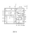
[接合裝置] 圖4為表示與一實施型態有關之接合裝置的俯視圖。圖5為表示與一實施型態有關之接合裝置的側視圖。[Joining device]Figure 4 is a top view of a joining device related to an embodiment. Figure 5 is a side view of a joining device related to an embodiment.
如圖4所示般,接合裝置41具有能夠密閉內部之處理容器100。在處理容器100之搬運區域60側之側面,形成上晶圓W1、下晶圓W2及重合基板T之搬入搬出口101,在該搬入搬出口101設置有開關擋板102。As shown in Fig. 4, the
處理容器100之內部係藉由內壁103被區劃成搬運區域T1和處理區域T2。上述搬入搬出口101係被形成在搬運區域T1中之處理容器100之側面。再者,在內壁103也形成上晶圓W1、下晶圓W2及重合晶圓T之搬入搬出口104。The interior of the
在搬運區域T1從例如搬入搬出口101側依序排列配置晶圓搬運機構111、反轉機構130及位置調節機構120。In the transfer area T1 , for example, a
移轉部110係暫時性地載置上晶圓W1、下晶圓W2及重合晶圓T。移轉部110被形成例如2層,可以同時載置上晶圓W1、下晶圓W2及重合晶圓T中之任兩個。The
晶圓搬運機構111如圖4及圖5所示般,具有例如在垂直方向(Z軸方向)、水平方向(Y軸方向、X軸方向)及繞垂直軸移動自如的搬運臂。晶圓搬運機構111係在搬運區域T1內或搬運區域T1和處理區域T2之間,能夠搬運上晶圓W1、下晶圓W2及重合晶圓T。As shown in FIG. 4 and FIG. 5 , the
位置調節機構120調節上晶圓W1及下晶圓W2之水平方向的方向。具體而言,位置調節機構120具有:基台121,其具備保持上晶圓W1及下晶圓W2而使旋轉的無圖示之保持部,和檢測部122,其檢測上晶圓W1及下晶圓W2之槽口部之位置。位置調節機構120一面使被保持於基台121之上晶圓W1及下晶圓W2旋轉,一面使用檢測部122而檢測出上晶圓W1及下晶圓W2之槽口部之位置,依此調節槽口部之位置。依此,上晶圓W1及下晶圓W2之水平方向之方位被調節。The
反轉機構130使上晶圓W1之表背面反轉。具體而言,反轉機構130具有保持第1上晶圓W1之保持臂131。保持臂131在水平方向(X軸方向)延伸。再者,在保持臂131在例如4處設置有保持上晶圓W1之保持構件132。The reversing
保持臂131被支撐於具備例如馬達等之驅動部133。保持臂131藉由如此之驅動部133繞水平軸轉動自如。再者,保持臂131係以驅動部133為中心轉動自如,並且在水平方向(X軸方向)移動自如。在驅動部133之下方,設置具備有例如馬達等之其他的驅動部(無圖示)。藉由其他之驅動部,驅動部133可以沿著在垂直方向延伸之支持柱134在垂直方向移動。The holding
如此一來,被保持於保持構件132之上晶圓W1可以藉由驅動部133繞水平軸轉動,並且可以在垂直方向及水平方向移動。再者,被保持於保持構件132之上晶圓W1,可以以驅動部133為中心轉動而在位置調節機構120和後述上夾盤140之間移動。Thus, the wafer W1 held on the holding
在處理區域T2,設置從上方吸附保持上晶圓W1之上面(非接合面W1n)之上夾盤140,和載置下晶圓W2而從下方吸附保持下晶圓W2之下面(非接合面W2n)之下夾盤141。下夾盤141係被設置在上夾盤140之下方,構成能夠與上夾盤140對向配置。In the processing area T2, an
如圖5所示般,上夾盤140被保持於被設置在上夾盤140之上方的上夾盤保持部150。上夾盤保持部150被設置在處理容器100之頂棚面。上夾盤140經由上夾盤保持部150被固定在處理容器100。5 , the
在上夾盤保持部150設置攝像被保持於下夾盤141之下晶圓W2之上面(接合面W2j)的上部攝像部151。上部攝像部151使用例如CCD攝影機。The upper
下夾盤141被支持於被設置在下夾盤141之下方之第1下夾盤移動部160。第1下夾盤移動部160係如後述般,使下夾盤141在水平方向(X軸方向)移動。再者,第1下夾盤移動部160被構成使下夾盤141在垂直方向移動自如,並且能夠繞垂直軸旋轉。The
在第1下夾盤移動部160,設置攝像被保持於上夾盤140之上晶圓W1之下面(接合面W1j)的下部攝像部161(參照圖5)。下部攝像部161使用例如CCD攝影機。The first lower
第1下夾盤移動部160被設置在第1下夾盤移動部160之下面側,被安裝於在水平方向(X軸方向)延伸之一對軌道162、162。第1下夾盤移動部160被構成沿著軌道162移動自如。The first lower
一對軌道162、162被配設在第2下夾盤移動部163。第2下夾盤移動部163被設置在第2下夾盤移動部163之下面側,被安裝於在水平方向(Y軸方向)延伸之一對軌道164、164。而且,第2下夾盤移動部163被構成沿著軌道164而在水平方向(Y軸方向)移動自如。另外,一對軌道164、164被配設在例如處理容器100之底面的載置台165上。A pair of
藉由第1下夾盤移動部160及第2下夾盤移動部163等,構成位置對準部166。位置對準部166係藉由使下夾盤141在X軸方向、Y軸方向及θ方向移動,進行被保持於上夾盤140之上晶圓W1,和被保持於下夾盤141之下晶圓W2之水平方向位置對準。再者,位置對準部166係藉由使下夾盤141在Z軸方向移動,進行被保持於上夾盤140之上晶圓W1,和被保持於下夾盤141之下晶圓W2之垂直方向位置對準。The first lower
另外,雖然本實施型態之位置對準部166係藉由使下夾盤141在X軸方向、Y軸方向及θ方向移動,進行上晶圓W1和下晶圓W2之水平方向位置對準,但是本發明不限定於此。位置對準部166若使上夾盤140和下夾盤141在X軸方向、Y軸方向及θ方向相對性地移動即可。例如,位置對準部166係藉由使下夾盤141在X軸方向及Y軸方向移動,並且使上夾盤140在θ方向移動,進行上晶圓W1和下晶圓W2之水平方向位置對準亦可。In addition, although the
再者,雖然本實施型態之位置對準部166係藉由使下夾盤141在Z軸方向移動,進行上晶圓W1和下晶圓W2之垂直方向位置對準,但是本發明不限定於此。位置對準部166若使上夾盤140和下夾盤141在Z軸方向相對性地移動即可。例如,即使位置對準部166藉由使上夾盤140在Z軸方向移動,進行上晶圓W1和下晶圓W2之垂直方向位置對準亦可。Furthermore, although the
圖6為與一實施型態有關之上夾盤及下夾盤之剖面圖,表示上晶圓和下晶圓將要接合之前之狀態的剖面圖。圖7(a)表示與一實施型態有關之上晶圓和下晶圓之接合途中之狀態的剖面圖。圖7(b)表示與一實施型態有關之上晶圓和下晶圓之接合完成時之狀態的剖面圖。在圖6、圖7(a)及圖7(b)中,以實線標示的箭頭表示藉由真空泵的空氣之吸引方向。FIG. 6 is a cross-sectional view of an upper chuck and a lower chuck related to an embodiment, showing a cross-sectional view of a state before the upper wafer and the lower wafer are joined. FIG. 7(a) shows a cross-sectional view of a state in the middle of joining the upper wafer and the lower wafer related to an embodiment. FIG. 7(b) shows a cross-sectional view of a state when the joining of the upper wafer and the lower wafer is completed related to an embodiment. In FIG. 6, FIG. 7(a) and FIG. 7(b), the arrows marked with solid lines show the direction of air suction by the vacuum pump.
上夾盤140及下夾盤141為例如真空夾盤。上夾盤140對應於專利申請範圍所載的保持部,下夾盤141對應於申請專利範圍所載的對向保持部。上夾盤140在與下夾盤141對向之面(下面)具有吸附上晶圓W1之吸附面140a。另外,下夾盤141在與上夾盤140對向之面(上面)具有吸附下晶圓W2之吸附面141a。The
上夾盤140具有夾盤基座170。夾盤基座170具有與上晶圓W1相同直徑或較上晶圓W1大的直徑。夾盤基座170藉由支持構件180被支持。支持構件180被設置成在俯視下至少覆蓋夾盤基座170,藉由例如螺絲緊固被固定在夾盤基座170。支持構件180被支持於被設置在處理容器100之頂棚面之複數支持柱181(參照圖5)。以支持構件180及複數支持柱181構成上夾保持部150。The
在支持構件180及夾盤基座170,形成在垂直方向貫通支持構件180及夾盤基座170之貫通孔176。貫通孔176之位置對應於被吸附保持於上夾盤140之上晶圓W1之中心部。在如此之貫通孔176被插通擊錘190之推壓銷191。A through
擊錘190被配置在支持構件180之上面,具備推壓銷191、致動器部192和直動機構193。推壓銷191係沿著垂直方向延伸之圓柱狀之構件,藉由致動器部192被支持。The
致動器部192係藉由從例如電動空氣調節器(無圖示)被供給之空氣,使在一定方向(在此為垂直下方)產生一定的壓力。致動器部192係藉由從電動空氣調節器被供給之空氣,與上晶圓W1之中心部抵接而可以控制施加於該上晶圓W1之中心部的推壓負載。再者,致動器部192之前端部藉由來自電動空氣調節器之空氣,插通貫通孔176而成為在垂直方向升降自如。The
致動器部192被支持於直動機構193。直動機構193係藉由內置例如馬達之驅動部使致動器部192在垂直方向移動。The
擊錘190係被構成上述般,藉由直動機構193控制致動器192之移動,而藉由致動器192控制推壓銷191所致的上晶圓W1之推壓負載。The
擊錘190係將被吸附保持於上夾盤140之上晶圓W1,和被吸附保持於下夾盤141之下晶圓W2對壓。具體而言,擊錘190係藉由使被吸附保持於上夾盤140之上晶圓W1變形,與下晶圓W2對壓。The
在夾盤基座170之下面設置與上晶圓W1之非接合面W1n接觸的複數插銷171。以夾盤基座170、複數插銷171等,構成上夾盤140。吸附上夾盤140之上晶圓W1的吸附面140a在徑向被區劃成複數區域,在被區劃的每個區域,進行吸附力的產生和吸附力的解除。A plurality of
另外,下夾盤141被構成與上夾盤140相同即可。下夾盤141具有與下晶圓W2之非接合面W2n接觸之複數插銷204。吸附保持下夾盤141之下晶圓W2的吸附面141a在徑向被區劃成複數區域,在被區劃的每個區域,進行吸附力的產生和吸附力的解除。In addition, the
[接合方法] 圖8為表示與一實施型態有關之接合系統所實行之處理之一部分的流程圖。另外,圖8所示之各種處理係在藉由控制裝置70之控制下被實行。[Joining method]FIG. 8 is a flow chart showing a part of the processing performed by a joining system related to an embodiment. In addition, the various processing shown in FIG. 8 is performed under the control of the
首先,收容複數片上晶圓W1之卡匣CS1、收容複數片下晶圓W2之卡匣CS2,及空的卡匣CS3被載置於搬入搬出站2之特定載置板11。之後,藉由搬運裝置22取出卡匣CS1內之上晶圓W1,搬運至處理站3之第3處理區塊G3之遞移裝置50。First, the cassette CS1 containing a plurality of upper wafers W1, the cassette CS2 containing a plurality of lower wafers W2, and the empty cassette CS3 are placed on the
接著,上晶圓W1係藉由搬運裝置61被搬運至第1處理區塊G1之表面改質裝置30。在表面改質裝置30中,在例如特定減壓氛圍下,處理氣體亦即氧氣被激勵而被電漿化,且被離子化。該氧離子被照射至上晶圓W1之接合面W1j,該接合面W1j被電漿處理。依此,上晶圓W1之接合面W1j被改質(步驟S101)。Next, the upper wafer W1 is transported to the
接著,上晶圓W1係藉由搬運裝置61被搬運至第2處理區塊G2之表面親水化裝置40。在表面親水化裝置40中,一面使被保持於旋轉夾盤之上晶圓W1旋轉,一面對該第1基板W1上供給純水。如此一來,被供給之純水在上晶圓W1之接合面W1j上擴散,在表面改質裝置30被改質之上晶圓W1之接合面W1j附著羥基(矽烷醇)而該接合面W1j被親水化(步驟S102)。再者,藉由接合面W1j之親水化使用的純水,上晶圓W1之接合面W1j被洗淨。Next, the upper wafer W1 is transported to the
接著,上晶圓W1係藉由搬運裝置61被搬運至第2處理區塊G2之接合裝置41。被搬入至接合裝置41之上晶圓W1係經移轉部110而藉由晶圓搬運機構111而被搬運至位置調節機構120。而且,藉由位置調節機構120,調節上晶圓W1之水平方向的方位(步驟S103)。Next, the upper wafer W1 is transported to the
之後,上晶圓W1從位置調節機構120被收授至反轉機構130之保持臂131。接著,在搬運區域T1,藉由使保持臂131反轉,上晶圓W1之表背面被反轉(步驟S104)。即是,上晶圓W1之接合面W1j朝下方。Afterwards, the upper wafer W1 is transferred from the
之後,反轉機構130之保持臂131轉動而朝上夾盤140之下方移動。而且,上晶圓W1從反轉機構130被收授至上夾盤140。上晶圓W1係在使槽口部朝向事先決定之方向的狀態,其非接合面W1n被吸附保持於上夾盤140(步驟S105)。Then, the holding
在上晶圓W1被進行上述步驟S101~S105之處理之期間,進行下晶圓W2的處理。首先,藉由搬運裝置22取出卡匣CS2內之下晶圓W2,被搬運至處理站3之移轉裝置50。While the upper wafer W1 is being processed in the above steps S101 to S105 , the lower wafer W2 is processed. First, the lower wafer W2 in the cassette CS2 is taken out by the
接著,下晶圓W2藉由搬運裝置61被搬運至表面改質裝置30,下晶圓W2之接合面W2j被改質(步驟S106)。另外,在步驟S106之下晶圓W2之接合面W2j之改質與上述步驟S101相同。Next, the lower wafer W2 is transported to the
接著,下晶圓W2藉由搬運裝置61被搬運至表面親水化裝置40,下晶圓W2之接合面W2j被親水化(步驟S107)。再者,藉由接合面W2j之親水化使用的純水,接合面W2j被洗淨。另外,在步驟S107之下晶圓W2之接合面W2j之親水化與在上述步驟S102之上晶圓W1之接合面W1j之親水化相同。Next, the lower wafer W2 is transported to the
之後,下晶圓W2藉由搬運裝置61被搬運至接合裝置41。被搬入至接合裝置41之下晶圓W2係經移轉部110而藉由晶圓搬運機構111而被搬運至位置調節機構120。而且,藉由位置調節機構120,調節下晶圓W2之水平方向的方位(步驟S108)。Afterwards, the lower wafer W2 is transported to the
之後,下晶圓W2藉由晶圓搬運機構111被搬運至下夾盤141,被吸附保持至下夾盤141(步驟S109)。下晶圓W2係在槽口部朝向事先設定的方向,即是與上晶圓W1之槽口部相同之方向的狀態,其非接合面W2n被吸附保持在下夾盤141。Afterwards, the lower wafer W2 is transported to the
接著,進行被保持於上夾盤140之上晶圓W1和被保持於下夾盤141之下晶圓W2之水平方向之位置調節(步驟S110)。具體而言,以在垂直方向觀看,被形成在上晶圓W1之接合面W1j之複數對準標記,和被形成在下晶圓W2之接合面W2j的複數對準標記重疊之方式,調節水平方向位置(例如,包含X軸方向位置、Y軸方向位置及θ方向位置)。Next, the horizontal position of the wafer W1 held on the
接著,進行被保持於上夾盤140之上晶圓W1和被保持於下夾盤141之下晶圓W2之垂直方向位置之調節(步驟S111)。具體而言,藉由第1下夾盤移動部160使下夾盤141在垂直上方移動,使下晶圓W2接近於上晶圓W1。依此,如圖6所示般,下晶圓W2之接合面W2j和上晶圓W1之接合面W1j之間隔S,被調整成特定距離,例如50μm~200μm。Next, the vertical positions of the wafer W1 held on the
接著,於解除藉由上夾盤140對上晶圓W1之中央部的吸附保持之後(步驟S112),如圖7(a)所示般,藉由使擊錘190之推壓銷191下降,下壓上晶圓W1之中心部(步驟S113)。當上晶圓W1之中心部接觸於下晶圓W2之中心部,上晶圓W1之中心部和下晶圓W2之中心部以特定之力被推壓時,在被推壓之上晶圓W1之中心部和下晶圓W2之中心部之間,開始接合。之後,產生從中心部朝向外周部慢慢地接合上晶圓W1和下晶圓W2的接合波。Next, after releasing the suction and holding of the center of the upper wafer W1 by the upper chuck 140 (step S112), as shown in FIG. 7(a), the center of the upper wafer W1 is pressed down by lowering the
在此,因上晶圓W1之接合面W1j和下晶圓W2之接合面W2j分別在步驟S101、S106被改質,故首先在接合面W1j、W2j間產生凡得瓦(Van der Waals')力(分子間力),該接合面W1j、W2j被接合。在此,因上晶圓W1之接合面W1j和下晶圓W2之接合面W2j分別在步驟S102、S107被親水化,故首先在接合面W1j、W2j間之親水基產生氫鍵,接合面W1j、W2j被緊固接合。Here, since the bonding surface W1j of the upper wafer W1 and the bonding surface W2j of the lower wafer W2 are modified in steps S101 and S106, respectively, Van der Waals' force (intermolecular force) is first generated between the bonding surfaces W1j and W2j, and the bonding surfaces W1j and W2j are bonded. Here, since the bonding surface W1j of the upper wafer W1 and the bonding surface W2j of the lower wafer W2 are hydrophilized in steps S102 and S107, respectively, hydrogen bonds are first generated in the hydrophilic groups between the bonding surfaces W1j and W2j, and the bonding surfaces W1j and W2j are firmly bonded.
之後,在藉由推壓銷191推壓上晶圓W1之中心部和下晶圓W2之中心部之狀態,解除藉由上夾盤140吸附保持上晶圓W1全體(步驟S114)。依此,如圖7(b)所示般,上晶圓W1之接合面W1j和下晶圓W2之接合面W2j以全面抵接,上晶圓W1和下晶圓W2被接合。之後,使推壓銷191上升至上夾盤140,解除藉由下夾盤141吸附保持下晶圓W2。Afterwards, the center of the upper wafer W1 and the center of the lower wafer W2 are pushed by the
之後,重合基板T藉由搬運裝置61被搬運至第3處理區塊G3之移轉裝置51,之後,藉由搬入搬出站2之搬運裝置22被搬運至卡匣CS3。如此一來,結束一連串之接合處理。Thereafter, the superimposed substrate T is transported to the
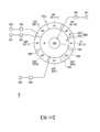
[控制下夾盤所致的下晶圓之歪斜] 圖9為表示與一實施型態有關之下夾盤、真空泵及真空調節器的圖示。在圖9中,表示在下夾盤141之吸附面141a之水平方向角度,和被吸附於其吸附面141a之時的下晶圓W2(參照圖6)之方向指數。另外,下晶圓W2之接合面W2j之面指數為(100)。作為方向指數或面指數使用的米勒指數為負,通常藉由在數字上標示「-」(槓)來表現,在本說明書中,以在數字之前標示負的符號來表現。另外,在圖9中,為了溶液觀看圖面,省略插銷204之圖示。[Control of the skew of the lower wafer caused by the lower chuck] FIG. 9 is a diagram showing a lower chuck, a vacuum pump, and a vacuum regulator related to an embodiment. FIG. 9 shows the horizontal angle of the
下夾盤141係如圖6等所示般,在吸附下晶圓W2之吸附面141a,具有圓狀之第1區域210及被配置在第1區域210之徑向外側的圓環狀之第2區域220,作為吸附下晶圓W2之吸附壓力(例如真空壓力)被獨立控制的複數區域。例如,下夾盤141係在吸附面141a具有區劃第1區域210和第2區域220之內周肋201、被配置在第2區域220之徑向外側的外周肋202。As shown in FIG. 6 and other figures, the
內周肋201和外周肋202係同心圓狀地突出設置在夾盤基座203之上面。在夾盤基座203之上面,散佈並突出設置與內周肋201或外周肋202相同高度之複數插銷204。內周肋201、外周肋202及複數插銷204具有相同高度,將下晶圓W2保持水平。The
再者,下夾盤141具有在徑向分割第2區域220而構成的複數環狀區域221、222,作為吸附下晶圓W2之吸附壓力被獨立控制的複數區域。例如,下夾盤141在吸附面141a具有區劃徑向方向外側之環狀區域221和徑向內側之環狀區域222之圓環狀的中間肋205。中間肋205被配置成與內周肋201或外周肋202呈同心圓狀。中間肋205具有與內周肋201或外周肋202相同的高度,與內周肋201或外周肋202一起將下晶圓W2保持水平。Furthermore, the
再者,下夾盤141如圖9所示般,具有在圓周方向分割第2區域220之外周端(即是,徑向最外側之環狀區域221)而構成的複數圓弧區域A1、A2,作為吸附下晶圓W2之吸附壓力被獨立控制的複數區域。兩個圓弧區域A1、A2在圓周方向彼此重複配置,例如各配置4個。例如,下夾盤141在吸附面141a具有區劃兩個圓弧區域A1、A2之分割肋206。分割肋206以放射狀地配置複數(例如8個)。分割肋206具有與內周肋201或外周肋202相同的高度,與內周肋201或外周肋202一起將下晶圓W2保持水平。在各圓弧區域A1、A2散佈且配置複數插銷204。Furthermore, as shown in FIG. 9 , the
並且,下夾盤141具有在圓周方向分割徑向內側之環狀區域222而構成的複數圓弧區域B1、B2,作為吸附下晶圓W2之吸附壓力被獨立控制的複數區域。兩個圓弧區域B1、B2在圓周方向彼此重複配置,例如各配置4個。例如,下夾盤141在吸附面141a具有區劃兩個圓弧區域B1、B2之分割肋207。分割肋207以放射狀地配置複數(例如8個)。分割肋207具有與內周肋201或外周肋202相同的高度,與內周肋201或外周肋202一起將下晶圓W2保持水平。在各圓弧區域B1、B2散佈且配置複數插銷204。Furthermore, the
接合裝置41具有例如複數真空泵231~234、241,作為構成下夾盤141之吸附面141a的複數區域各自產生吸附壓力的複數吸附壓力產生部。再者,接合裝置41具有例如複數真空調節器251~254、261,作為獨立調整藉由複數真空泵231~234、241分別產生之吸附壓力之複數吸附壓力調整部。The
一個真空泵231經由在途中設置一個真空調節器251之配管而與4個圓弧區域A1連接(在圖9中,僅圖示與一個圓弧區域A1連接之配管)。同樣,一個真空泵232經由在途中設置一個真空調節器252之配管而與4個圓弧區域A2連接(在圖9中,僅圖示與一個圓弧區域A2連接之配管)。再者,一個真空泵233經由在途中設置一個真空調節器253之配管而與4個圓弧區域B1連接(在圖9中,僅圖示與一個圓弧區域B1連接之配管)。同樣,一個真空泵234經由在途中設置一個真空調節器254之配管而與4個圓弧區域B2連接(在圖9中,僅圖示與一個圓弧區域B2連接之配管)。並且,一個真空泵241係經由在途中設置一個真空調節器261之配管而與第1區域210連接。A
當控制裝置70使一個真空泵231作動時, 一個真空泵231使4個圓弧區域A1產生真空壓力,其真空壓力在真空調節器251以事先設定的設定值被維持,在4個圓弧區域A1產生與其設定值對應之吸附壓力。真空設定調節器251之設定值能夠藉由控制裝置70變更,以大氣壓為基準在例如-80kPa~-5kPa之範圍被設定。另外,當控制裝置70使真空泵231之作動停止時,4個圓弧區域A1返回至大氣壓,解除在4個圓弧區域A4產生吸附壓力。因在其他的圓弧區域A2、圓弧區域B1、圓弧區域B2及第1區域210產生及解除吸附壓力,與在圓弧區域A1產生及解除吸附壓力相同,故省略說明。When the
本實施型態之接合裝置41具有控制複數真空泵231~234、241及複數真空調節器251~254、261的控制裝置70。雖然控制裝置70被設置在圖1等中接合裝置41之外部,即使作為接合裝置41之一部分而被設置亦可。控制裝置70與專利申請範圍所記載之控制部對應。The
本實施型態之控制裝置70係使第1區域210之至少一部分(例如,第1區域210之全體)和第2區域220之至少一部分(例如,圓弧區域A2及圓弧區域B1)同時產生不同的吸附壓力。依此,可以控制在吸附面141a產生的吸附壓力之徑向中的分布,可以控制在被吸附於吸附面141a之下晶圓W2產生的歪斜。The
即使在第1區域210產生的吸附壓力,和在圓弧區域A2及圓弧區域B1產生的吸附壓力中之一個較大亦可,即使其中之一個較小亦可。並且,雖然在第1區域210產生的吸附壓力,和在圓弧區域A1及圓弧區域B2產生的吸附壓力,在本實施型態中為相同,但是即使其中之一個較大亦可,即使其中之一個較小亦可。再者,即使在圓弧區域A1及圓弧區域B2,在吸附面141a吸附下晶圓W2之時不產生吸附壓力亦可。即是,雖然在本實施型態中,吸附下晶圓W2之時,在吸附面141a之全體同時產生吸附壓力,但是即使僅使吸附面141a之一部分產生吸附壓力亦可。Even if one of the adsorption pressure generated in the
若藉由本實施型態時,可以一面控制在下晶圓W2產生的歪斜,一面接合下晶圓W2和上晶圓W1,可以降低下晶圓W2和上晶圓W1之貼合歪斜(Distortion)。貼合歪斜係以例如使上晶圓W1和下晶圓W2相對性平行移動、旋轉移動及相似伸縮,使被形成在上晶圓W1之複數對準標記和被形成在下晶圓W2之複數對準標記在俯視下的位置偏移成為最小之時殘留的位置偏移之大小來表示。重複進行吸附壓力之設定的變更,和依照變更後之設定而進行的接合,和接合後之貼合歪斜之測定,直至貼合歪斜落入容許範圍內即可。即使吸附壓力之分布的變更係根據過去存儲的複數資料而進行亦可。資料若表示吸附壓力之設定(或實績)和貼合歪斜之關係者即可,讀出並使用被記憶於資訊記憶媒體者。By using this embodiment, the skew generated in the lower wafer W2 can be controlled while the lower wafer W2 and the upper wafer W1 are bonded, so that the bonding distortion of the lower wafer W2 and the upper wafer W1 can be reduced. The bonding distortion is represented by the size of the residual positional offset when the positional offset of the multiple alignment marks formed on the upper wafer W1 and the multiple alignment marks formed on the lower wafer W2 when viewed from above is minimized, for example, by making the upper wafer W1 and the lower wafer W2 relatively parallel move, rotationally move, and similarly stretch. The setting change of the adsorption pressure, the bonding according to the changed setting, and the measurement of the bonding distortion after bonding are repeated until the bonding distortion falls within the allowable range. It is also acceptable even if the change in the distribution of the adsorption pressure is made based on multiple data stored in the past. Data that indicates the relationship between the setting (or actual performance) of the adsorption pressure and the lamination skewness may be read out and used if it is stored in the information storage medium.
本發明者精心研究研究之結果,找出貼合歪斜之一原因在於下晶圓W2之楊氏係數之物性的各向異性。下晶圓W2之楊氏係數等之物性在圓周方向周期性地變化。藉由該變化而產生的貼合歪斜從下晶圓W2之徑向內側越朝徑向外側越明顯。因為從下晶圓W2之徑向內側越朝徑向外側,例如在[0-11]方向和[001]方向之圓周方向的距離越分離之故。The inventor of the present invention has carefully studied and found that one of the reasons for the bonding skew is the anisotropy of the physical properties of the Young's modulus of the lower wafer W2. The physical properties of the Young's modulus of the lower wafer W2 change periodically in the circumferential direction. The bonding skew caused by this change becomes more obvious from the inner diameter of the lower wafer W2 to the outer diameter. This is because the distance in the circumferential direction of, for example, the [0-11] direction and the [001] direction becomes more and more separated from the inner diameter of the lower wafer W2 to the outer diameter.
於是,本實施型態之控制裝置70係使被配置在第1區域210之徑向外側之第2區域220之一部分(例如,圓弧區域A1及圓弧區域B2)和第2區域220之其他之一部分(例如圓弧區域A2及圓弧區域B1)同時產生不同的吸附壓力。依此,可以控制在偏離下晶圓W2之中心的第2區域220,產生在下晶圓W2的歪斜。Therefore, the
即使在圓弧區域A1及圓弧區域B2產生的吸附壓力,和在圓弧區域A2及圓弧區域B1產生的吸附壓力中之一個較大亦可,其中一個較小亦可。並且,雖然在圓弧區域A1產生的吸附壓力,和在圓弧區域B2產生的吸附壓力在本實施型態中為相同,但是即使其中之一個較大亦可。即使其中之一個較小亦可。同樣,雖然在圓弧區域A2產生的吸附壓力,和在圓弧區域B1產生的吸附壓力在本實施型態中為相同,但是即使其中之一個較大亦可。即使其中之一個較小亦可。Even if one of the adsorption pressures generated in the arc area A1 and the arc area B2 and the adsorption pressures generated in the arc area A2 and the arc area B1 is larger, it is also acceptable. Moreover, although the adsorption pressure generated in the arc area A1 and the adsorption pressure generated in the arc area B2 are the same in this embodiment, it is also acceptable if one of them is larger. It is also acceptable if one of them is smaller. Similarly, although the adsorption pressure generated in the arc area A2 and the adsorption pressure generated in the arc area B1 are the same in this embodiment, it is also acceptable if one of them is larger. It is also acceptable if one of them is smaller.
本實施型態之控制裝置70係使在徑向分割第2區域220而構成的複數環狀區域221、222之中,徑向外側之環狀區域221之至少一部分(例如,圓弧區域A1),和徑向內側之環狀區域222之至少一部分(例如圓弧區域B1)同時產生不同的吸附壓力。依此,可以控制根據從下晶圓W2之中心的徑向距離產生在下晶圓W2的歪斜。The
本實施型態之控制裝置70係在於圓周方向分割第2區域220之外周端而構成的複數圓弧區域之中相鄰的圓弧區域(在此,為徑向最外側之環狀區域221所含的圓弧區域A1和圓弧區域A2),獨立控制吸附壓力,並且同時產生不同的吸附壓力。因為下晶圓W2之楊氏係數等之物性在圓周方向周期性地變化,藉由其變化而產生的貼合歪斜在下晶圓W2之外周端最為明顯之故。The
同樣,控制裝置70即使在圓周方向分割剩下的環狀區域(在此,徑向內側之環狀區域222)而構成的複數圓弧區域之中相鄰的圓弧區域(例如,圓弧區域B1和圓弧區域B2),獨立控制吸附壓力,並且同時產生不同的吸附壓力亦可。不僅徑向外側之環狀區域221,亦可以在徑向內側之環狀區域222控制下晶圓W2之歪斜。在下晶圓W2之直徑大之情況特別有效。Similarly, the
然而,單晶矽晶圓之楊氏係數、浦松氏比(Poisson's ratio)、剪切彈性係數係以90°周期變化。以[0-11] 方向(0°方向)為基準的90°周期之方向(0°方向、90°方向、180°方向及270°方向)總稱為「0°基準90°周期方向」。再者,以[0-10]方向(45°方向)為基準的90°周期之方向(45°方向、135°方向、225°方向及315°方向)總稱為「45°基準90°周期方向」。單晶矽晶圓之楊氏係數在0°基準90°周期方向最高,在45°基準90°周期方向最低。再者,針對浦松氏比及剪切彈性係數,在45°基準90°周期方向最高,在0°基準90°周期方向最低。However, the Young's modulus, Poisson's ratio, and shear elastic modulus of a single crystal silicon wafer vary in a 90° periodicity. The directions of the 90° periodicity (0° direction, 90° direction, 180° direction, and 270° direction) based on the [0-11] direction (0° direction) are collectively referred to as the "0° reference 90° periodicity directions." Furthermore, the directions of the 90° periodicity (45° direction, 135° direction, 225° direction, and 315° direction) based on the [0-10] direction (45° direction) are collectively referred to as the "45° reference 90° periodicity directions." The Young's modulus of a single crystal silicon wafer is highest in the 0° reference 90° periodicity directions and lowest in the 45° reference 90° periodicity directions. Furthermore, for the Pu Song ratio and shear elastic coefficient, the highest is in the 45° base 90° period direction, and the lowest is in the 0° base 90° period direction.
於是,在下晶圓W2為單晶矽晶圓之情況,如圖9所示般,在0°基準90°周期方向配置圓弧區域A1,在45°基準90°周期方向配置圓弧區域A2即可。即是,吸附壓力被獨立控制之兩個圓弧區域A1、A2在圓周方向彼此重複配置,例如各配置4個。Therefore, when the lower wafer W2 is a single crystal silicon wafer, as shown in FIG9 , the arc region A1 is arranged in the 90° period direction of the 0° reference, and the arc region A2 is arranged in the 90° period direction of the 45° reference. That is, the two arc regions A1 and A2 whose adsorption pressure is independently controlled are arranged repeatedly in the circumferential direction, for example, 4 of each are arranged.
同樣,在下晶圓W2為單晶矽晶圓之情況,如圖9所示般,在0°基準90°周期方向配置圓弧區域B1,在45°基準90°周期方向配置圓弧區域B2即可。即是,吸附壓力被獨立控制之兩個圓弧區域B1、B2在圓周方向彼此重複配置,例如各配置4個。Similarly, when the lower wafer W2 is a single crystal silicon wafer, as shown in FIG9 , the arc region B1 is arranged in the 90° period direction of the 0° reference, and the arc region B2 is arranged in the 90° period direction of the 45° reference. That is, the two arc regions B1 and B2 whose adsorption pressure is independently controlled are arranged repeatedly in the circumferential direction, for example, 4 arc regions are arranged in each direction.
另外,雖然本實施型態之控制裝置70係使在角度相同的複數圓弧區域(例如,圓弧區域A1和圓弧區域B1、或圓弧區域A2和圓弧區域B2)同時產生不同的吸附壓力,但是本發明不限定於此。例如,即使控制裝置70使在角度不同之複數圓弧區域(例如,圓弧區域A1和圓弧區域B2,或是圓弧區域A2和圓弧區域B1)產生不同的吸附壓力亦可。In addition, although the
[變形、改良] 以上,雖然針對基板處理裝置及基板處理方法之實施型態進行說明,但是本發明不限定於上述實施型態等,可以在申請專利範圍所記載之本發明之主旨的範圍內,進行各種變形、改良。[Variations and Improvements]Although the above describes the implementation forms of the substrate processing device and the substrate processing method, the present invention is not limited to the above implementation forms, etc. Various modifications and improvements can be made within the scope of the gist of the present invention described in the scope of the patent application.
雖然上述實施型態之控制裝置70係使相鄰之圓弧區域B1、B2中同時產生不同的吸附壓力,但是本發明不限定於此。即使控制裝置70在相鄰的圓弧區域B1、B2產生相同的吸附壓力亦可。在此情況,因徑向內側之環狀區域222無須在圓周方向分割複數圓弧區域B1、B2,故如圖10所示般,僅以一個圓環區域B構成即可。一個圓環區域B係經由在途中設置一個真空調節器253之配管而與一個真空泵233連接。因在圓環區域B產生及解除吸附壓力與在圓弧區域A1產生及解除吸附壓力相同,故省略說明。Although the
雖然上述實施型態之徑向外側之環狀區域221和徑向內側之環狀區域222被分割成在圓周方向相同數量,但是即使被分割成在圓周方向不同的數量亦可。如圖11所示般,即使徑向外側之環狀區域221之分割數量較徑向內側之環狀區域222之分割數量多亦可。因從下晶圓W2之徑向內側越朝向徑向外側,越容易產生貼合歪斜之故。Although the radially outer
圖11所示之下夾盤141具有在圓周方向分割徑向外側之環狀區域221而構成的3個圓弧區域A1、A2、A3,作為吸附壓力被獨立控制的複數區域。圓弧區域A3被配置在0°基準90°周期方向的圓弧區域A1,和被配置在45°基準90°周期方向之圓弧區域A2之間。依此,可以精度更佳地控制在下晶圓W2之圓周方向的吸附壓力分布。As shown in FIG. 11 , the
如圖11所示般,即使將徑向外側之環狀區域221在圓周方向分割成複數圓弧區域A1、A2、A3之分割線(例如,分割肋206),和將徑向內側之環狀區域222在圓周方向分割成複數圓弧區域B1、B2之分割線(例如,分割肋207)在圓周方向偏離亦可。可以使在徑向外側之環狀區域221中吸附壓力不連續變化之處,和在徑向內側之環狀區域222中吸附壓力不連續地變化之處,在圓周方向偏離。As shown in FIG. 11 , even if the dividing line (e.g., dividing rib 206) that divides the radially outer
如圖11所示之4個圓弧區域A3係經由在途中設置一個真空調節器255之配管而與一個真空泵235連接(在圖11中,僅圖示與一個圓弧區域A3連接的配管)。因在圓環區域A3產生及解除吸附壓力與在圓弧區域A1產生及解除吸附壓力相同,故省略說明。As shown in FIG11 , the four arc regions A3 are connected to a
雖然圖9~圖11所示之上夾盤141具有在徑向分割第2區域220而構成的兩個環狀區域221、222,作為吸附壓力被獨立控制之複數區域,但是環狀區域之數量不限定於兩個。環狀區域之數量即使為一個亦可(即是,第2區域220即使不被分割亦可),環狀區域之數量即使為3個以上亦可。Although the
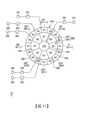
圖12為表示與第3變形例有關之下夾盤、真空泵及真空調節器的圖示。圖12所示之變形例之下夾盤141具有在徑向分割第2區域220而構成的4個環狀區域221、222、223、224,作為吸附壓力被獨立控制的複數區域。Fig. 12 is a diagram showing a lower chuck, a vacuum pump and a vacuum regulator related to the third modification. The
從徑向外側算起第1個之環狀區域221係由在圓周方向彼此交互重複排列之兩個圓弧區域A1、A2構成。相鄰的兩個圓弧區域A1、A2係吸附壓力被獨立控制。同樣,從徑向外側算起第2個之環狀區域222係由在圓周方向彼此交互重複排列之兩個圓弧區域B1、B2構成。相鄰的兩個圓弧區域B1、B2係吸附壓力被獨立控制。The first
再者,從徑向外側算起第3個之環狀區域223係由在圓周方向彼此交互重複排列之兩個圓弧區域C1、C2構成。相鄰的兩個圓弧區域C1、C2係吸附壓力被獨立控制。一個真空泵235經由在途中設置一個真空調節器255之配管而與4個圓弧區域C1連接(在圖12中,僅圖示與一個圓弧區域C1連接之配管)。一個真空泵236經由在途中設置一個真空調節器256之配管而與4個圓弧區域C2連接(在圖12中,僅圖示與一個圓弧區域C2連接之配管)。因在圓弧區域C1、C2產生及解除吸附壓力與在圓弧區域A1產生及解除吸附壓力相同,故省略說明。Furthermore, the third
並且,從徑向外側算起第4個之環狀區域224係由在圓周方向彼此交互重複排列之兩個圓弧區域D1、D2構成。相鄰的兩個圓弧區域D1、D2係吸附壓力被獨立控制。一個真空泵237經由在途中設置一個真空調節器257之配管而與4個圓弧區域D1連接(在圖12中,僅圖示與一個圓弧區域D1連接之配管)。一個真空泵238經由在途中設置一個真空調節器258之配管而與4個圓弧區域D2連接(在圖12中,僅圖示與一個圓弧區域D2連接之配管)。因在圓環區域D1、D2產生及解除吸附壓力與在圓弧區域A1產生及解除吸附壓力相同,故省略說明。Furthermore, the fourth
再者,圖12所示之變形例之下夾盤141具有在徑向分割第1區域210而構成的2個環狀區域211、212和一個圓區域213,作為吸附壓力被獨立控制的複數區域。徑向外側之環狀區域211和徑向內側之環狀區域212藉由圓環狀之肋部被區劃。再者,徑向內側之環狀區域212和圓區域213藉由圓環狀之肋部被區劃。被配置在第1區域210之內部的圓環狀之肋部被形成與圖9等所示之內周肋201或外周肋202同心圓狀。被配置在第1區域210之內部的圓環狀之肋部,具有與插銷204相同的高度,與插銷204等一起將下將圓W2保持水平。另外,在本變形例中,兩個區域211、212及圓區域213與申請專利範圍所載的分割區域對應。Furthermore, the
在第1區域210中從徑向外側算起第1個的環狀區域211,經由在途中設置一個真空調節器261之配管而與一個真空泵241連接。再者,在第1區域210中從徑向外側算起第2個的環狀區域212,經由在途中設置一個真空調節器262之配管而與一個真空泵242連接。並且,在第1區域210中從徑向外側算起第3個的圓區域213,經由在途中設置一個真空調節器263之配管而與一個真空泵243連接。因在環狀區域211、212及圓區域213產生及解除吸附壓力與在圓弧區域A1產生及解除吸附壓力相同,故省略說明。The first
本變形例之控制裝置70係使相鄰的兩個分割區域(例如,徑向外側之環狀區域211和徑向內側之環狀區域212,及/或徑向內側之環狀區域212和圓區域213)同時產生不同的吸附壓力。依此,可以控制以擊錘190之推壓銷191被推壓的下晶圓W2之中心部附近之歪斜。The
另外,構成第1區域210之環狀區域之數量雖然在圖12中為兩個,但是即使為一個亦可,即使為3個以上亦可。再者,構成第1區域210之環狀區域(例如,環狀區域211)與構成第2區域220之環狀區域(例如,環狀區域221)相同,即使在圓周方向分割成複數區域亦可。In addition, although the number of annular regions constituting the
雖然上述實施型態及上述變形例之下夾盤141真空吸附下晶圓W2,但是即使靜電吸附亦可。在此情況,吸附壓力產生部包含被埋設在下吸盤141之內部的內部電極。另外,吸附壓力調整部包含例如調整供給至內部電極之電力的電力調整部。電力調整部係由例如降壓型DC/DC轉換器或升壓型DC/DC轉換器等構成。Although the
在上述實施型態及上述變形例中,雖然控制產生在被吸附於下夾盤141之下晶圓W2的歪斜,但是即使控制產生在被吸附於上夾盤140之上晶圓W1的歪斜亦可。即是,即使將本發明適用於上夾盤140亦可,即使對應於專利申請範圍所載的保持部,下夾盤141對應於申請專利範圍所載的對向保持部亦可。再者,即使將本發明適用於上夾盤140和下夾盤141之雙方亦可。並且,即使將本發明適用於接合裝置41以外之裝置,例如切割裝置等亦可。若本發明為具有保持基板之保持部的裝置則可以適用。In the above-mentioned embodiment and the above-mentioned variation, although the deflection of the wafer W2 adsorbed on the
41:接合裝置 70:控制裝置 140:上夾盤(對向保持部) 141:下夾盤(保持部) 141a:吸附面 210:第1區域 220:第2區域 221:徑向外側之環狀區域 222:徑向內側之環狀區域 231~234、241:真空泵(吸附壓力產生部) 251~254、261:真空調節器(吸附壓力調整部) W1:上晶圓(基板) W2:下晶圓(基板)41: Bonding device70: Control device140: Upper chuck (opposite holding part)141: Lower chuck (holding part)141a: Adsorption surface210: First area220: Second area221: Annular area on the radial outer side222: Annular area on the radial
[圖1]為表示與一實施型態有關之接合系統的俯視圖。 [圖2]為表示與一實施型態有關之接合系統的側視圖。 [圖3]為表示與一實施型態有關之第1基板及第2基板之接合前之狀態的側視圖。 [圖4]為表示與一實施型態有關之接合裝置的俯視圖。 [圖5]為表示與一實施型態有關之接合裝置的側視圖。 [圖6]為表示與一實施型態有關之上夾盤及下夾盤之剖面圖,於上晶圓和下晶圓之位置對準之後,接合前之狀態的剖面圖。 [圖7]為表示從中心部朝向外周部慢慢地接合與一實施型態有關之上晶圓和下晶圓的剖面圖。 [圖8]為表示與一實施型態有關之接合系統所實行之處理之一部分的流程圖。 [圖9]為表示與一實施型態有關之下夾盤、真空泵及真空調節器的圖示。 [圖10]為表示與第1變形例有關之下夾盤、真空泵及真空調節器的圖示。 [圖11]為表示與第2變形例有關之下夾盤、真空泵及真空調節器的圖示。 [圖12]為表示與第3變形例有關之下夾盤、真空泵及真空調節器的圖示。[FIG. 1] is a top view of a bonding system according to an embodiment.[FIG. 2] is a side view of a bonding system according to an embodiment.[FIG. 3] is a side view of a state before bonding of a first substrate and a second substrate according to an embodiment.[FIG. 4] is a top view of a bonding device according to an embodiment.[FIG. 5] is a side view of a bonding device according to an embodiment.[FIG. 6] is a cross-sectional view of an upper chuck and a lower chuck according to an embodiment, and is a cross-sectional view of a state before bonding after the positions of the upper wafer and the lower wafer are aligned.[FIG. 7] is a cross-sectional view showing that the upper wafer and the lower wafer according to an embodiment are bonded gradually from the center toward the periphery.[FIG. 8] is a flow chart showing a part of the processing performed by the joining system related to an embodiment.[FIG. 9] is a diagram showing a lower chuck, a vacuum pump, and a vacuum regulator related to an embodiment.[FIG. 10] is a diagram showing a lower chuck, a vacuum pump, and a vacuum regulator related to the first variant.[FIG. 11] is a diagram showing a lower chuck, a vacuum pump, and a vacuum regulator related to the second variant.[FIG. 12] is a diagram showing a lower chuck, a vacuum pump, and a vacuum regulator related to the third variant.
141a:吸附面141a: Adsorption surface
201:內周肋201: Inner ribs
202:外周肋202: Peripheral ribs
205:中間肋205: Middle rib
206:分割肋206: Split ribs
207:分割肋207: Split ribs
210:第1區域210:
220:第2區域220:
221:徑向外側之環狀區域221: Annular area extending outward
222:徑向內側之環狀區域222: Annular area with inner diameter
231~234、241:真空泵(吸附壓力產生部)231~234, 241: Vacuum pump (adsorption pressure generating part)
251~254、261:真空調節器(吸附壓力調整部)251~254, 261: Vacuum regulator (adsorption pressure adjustment unit)
Claims (8)
Translated fromChineseApplications Claiming Priority (2)
| Application Number | Priority Date | Filing Date | Title |
|---|---|---|---|
| JP2018-005987 | 2018-01-17 | ||
| JP2018005987 | 2018-01-17 |
Publications (2)
| Publication Number | Publication Date |
|---|---|
| TW202401630A TW202401630A (en) | 2024-01-01 |
| TWI846591Btrue TWI846591B (en) | 2024-06-21 |
Family
ID=67302315
Family Applications (2)
| Application Number | Title | Priority Date | Filing Date |
|---|---|---|---|
| TW112134471ATWI846591B (en) | 2018-01-17 | 2019-01-02 | Bonding device and bonding method |
| TW108100018ATWI818942B (en) | 2018-01-17 | 2019-01-02 | Joining device and joining method |
Family Applications After (1)
| Application Number | Title | Priority Date | Filing Date |
|---|---|---|---|
| TW108100018ATWI818942B (en) | 2018-01-17 | 2019-01-02 | Joining device and joining method |
Country Status (6)
| Country | Link |
|---|---|
| US (1) | US11735465B2 (en) |
| JP (2) | JP6918986B2 (en) |
| KR (2) | KR20240074887A (en) |
| CN (2) | CN111566782B (en) |
| TW (2) | TWI846591B (en) |
| WO (1) | WO2019142708A1 (en) |
Families Citing this family (8)
| Publication number | Priority date | Publication date | Assignee | Title |
|---|---|---|---|---|
| WO2021054265A1 (en)* | 2019-09-20 | 2021-03-25 | 東京エレクトロン株式会社 | Joining device and joining method |
| JP2021086989A (en)* | 2019-11-29 | 2021-06-03 | 東京エレクトロン株式会社 | Vacuum chuck and joint device |
| JP7488062B2 (en)* | 2020-03-02 | 2024-05-21 | 東京エレクトロン株式会社 | Bonding device, bonding system, bonding method, and storage medium |
| TW202139060A (en)* | 2020-04-01 | 2021-10-16 | 政美應用股份有限公司 | Wafer image capturing apparatus and image capturing method thereof |
| CN112038220B (en)* | 2020-08-31 | 2023-02-03 | 上海华力集成电路制造有限公司 | Method for improving wafer edge deformation in wafer bonding process |
| JP7717553B2 (en) | 2021-09-17 | 2025-08-04 | キオクシア株式会社 | Joining device and joining method |
| US20230178397A1 (en)* | 2021-12-06 | 2023-06-08 | Skyworks Solutions, Inc. | Wafer cleaning with wafer assembly presence detection |
| JP2025528775A (en)* | 2022-08-16 | 2025-09-02 | 東京エレクトロン株式会社 | Wafer bonding process with reduced overlay distortion |
Citations (3)
| Publication number | Priority date | Publication date | Assignee | Title |
|---|---|---|---|---|
| WO2011111565A1 (en)* | 2010-03-09 | 2011-09-15 | 東京エレクトロン株式会社 | Joining system, joining method, program and computer memory media |
| WO2012121046A1 (en)* | 2011-03-04 | 2012-09-13 | 東京エレクトロン株式会社 | Bonding device, bonding system and bonding method |
| US20160155721A1 (en)* | 2014-11-27 | 2016-06-02 | Tokyo Electron Limited | Bonding Method, Storage Medium, Bonding Apparatus and Bonding System |
Family Cites Families (18)
| Publication number | Priority date | Publication date | Assignee | Title |
|---|---|---|---|---|
| KR20010024969A (en)* | 1999-02-02 | 2001-03-26 | 마에다 시게루 | Wafer holder and polishing device |
| JP2005136025A (en)* | 2003-10-29 | 2005-05-26 | Trecenti Technologies Inc | Semiconductor manufacturing apparatus, method of manufacturing semiconductor device, and wafer stage |
| JP4821091B2 (en)* | 2004-04-08 | 2011-11-24 | 株式会社ニコン | Wafer bonding equipment |
| JP6340693B2 (en)* | 2013-07-18 | 2018-06-13 | 株式会社ブイ・テクノロジー | Substrate holding device, contact exposure device, and proximity exposure device |
| JP5538613B1 (en) | 2013-11-13 | 2014-07-02 | 東京エレクトロン株式会社 | Joining apparatus and joining system |
| JP6244188B2 (en)* | 2013-11-27 | 2017-12-06 | 東京エレクトロン株式会社 | Joining apparatus, joining method and joining system |
| JP6177739B2 (en)* | 2014-08-07 | 2017-08-09 | 東京エレクトロン株式会社 | Joining apparatus, joining system, joining method, program, and computer storage medium |
| JP6665405B2 (en)* | 2014-08-28 | 2020-03-13 | 大日本印刷株式会社 | Work adsorption method and device |
| JP6558646B2 (en)* | 2014-10-29 | 2019-08-14 | Agc株式会社 | Substrate adsorption device, substrate bonding apparatus and method, and electronic device manufacturing method |
| KR20240154103A (en)* | 2014-12-10 | 2024-10-24 | 가부시키가이샤 니콘 | Substrate stacking device and substrate stacking method |
| JP6568781B2 (en)* | 2015-04-04 | 2019-08-28 | 東京エレクトロン株式会社 | Substrate holding method, substrate holding apparatus, processing method and processing apparatus |
| WO2017104732A1 (en)* | 2015-12-18 | 2017-06-22 | 日本特殊陶業株式会社 | Substrate holding device, substrate holding member, and substrate holding method |
| JP6788678B2 (en)* | 2016-02-08 | 2020-11-25 | エーエスエムエル ネザーランズ ビー.ブイ. | Lithography equipment, how to unload a substrate, and how to load a substrate |
| JP6448848B2 (en)* | 2016-03-11 | 2019-01-09 | ボンドテック株式会社 | Substrate bonding method |
| JP6685154B2 (en)* | 2016-03-14 | 2020-04-22 | 東京エレクトロン株式会社 | Joining device and joining method |
| JP6727069B2 (en)* | 2016-08-09 | 2020-07-22 | 東京エレクトロン株式会社 | Joining device and joining system |
| JP6706182B2 (en)* | 2016-09-16 | 2020-06-03 | キオクシア株式会社 | Substrate holding device |
| JP6895770B2 (en)* | 2017-03-02 | 2021-06-30 | 東京エレクトロン株式会社 | Joining equipment and joining system |
- 2019
- 2019-01-02TWTW112134471Apatent/TWI846591B/enactive
- 2019-01-02TWTW108100018Apatent/TWI818942B/enactive
- 2019-01-09CNCN201980008044.XApatent/CN111566782B/enactiveActive
- 2019-01-09KRKR1020247015785Apatent/KR20240074887A/enactivePending
- 2019-01-09KRKR1020207022949Apatent/KR102668071B1/enactiveActive
- 2019-01-09CNCN202410680731.9Apatent/CN118748157A/enactivePending
- 2019-01-09JPJP2019566433Apatent/JP6918986B2/enactiveActive
- 2019-01-09USUS16/962,680patent/US11735465B2/enactiveActive
- 2019-01-09WOPCT/JP2019/000371patent/WO2019142708A1/ennot_activeCeased
- 2020
- 2020-05-07JPJP2020081978Apatent/JP6919019B2/enactiveActive
Patent Citations (3)
| Publication number | Priority date | Publication date | Assignee | Title |
|---|---|---|---|---|
| WO2011111565A1 (en)* | 2010-03-09 | 2011-09-15 | 東京エレクトロン株式会社 | Joining system, joining method, program and computer memory media |
| WO2012121046A1 (en)* | 2011-03-04 | 2012-09-13 | 東京エレクトロン株式会社 | Bonding device, bonding system and bonding method |
| US20160155721A1 (en)* | 2014-11-27 | 2016-06-02 | Tokyo Electron Limited | Bonding Method, Storage Medium, Bonding Apparatus and Bonding System |
Also Published As
| Publication number | Publication date |
|---|---|
| TWI818942B (en) | 2023-10-21 |
| US20200365442A1 (en) | 2020-11-19 |
| JP2020120138A (en) | 2020-08-06 |
| TW202401630A (en) | 2024-01-01 |
| WO2019142708A1 (en) | 2019-07-25 |
| JPWO2019142708A1 (en) | 2020-08-06 |
| KR20200100847A (en) | 2020-08-26 |
| CN111566782A (en) | 2020-08-21 |
| CN118748157A (en) | 2024-10-08 |
| CN111566782B (en) | 2024-06-11 |
| KR20240074887A (en) | 2024-05-28 |
| JP6918986B2 (en) | 2021-08-11 |
| TW202435340A (en) | 2024-09-01 |
| JP6919019B2 (en) | 2021-08-11 |
| TW201937630A (en) | 2019-09-16 |
| US11735465B2 (en) | 2023-08-22 |
| KR102668071B1 (en) | 2024-05-22 |
Similar Documents
| Publication | Publication Date | Title |
|---|---|---|
| TWI846591B (en) | Bonding device and bonding method | |
| TWI594308B (en) | Joining device, joining system, joining method, and computer storage medium | |
| TW201818449A (en) | Bonding device and bonding system | |
| JP6967980B2 (en) | Joining method and joining device | |
| JP6707420B2 (en) | Joining device and joining system | |
| JP6895770B2 (en) | Joining equipment and joining system | |
| TWI612595B (en) | Joining device, joining system, joining method and computer storage medium | |
| JP2021141115A (en) | Joining equipment, joining systems, joining methods and storage media | |
| JP2015018919A (en) | Joining device, joining system, joining method, program and computer storage medium | |
| JP2018190817A (en) | Joining apparatus and joining method | |
| JP6861872B2 (en) | Joining equipment and joining system | |
| TWI839869B (en) | Substrate processing device and substrate processing method | |
| JP2018026415A (en) | Bonding device and bonding system | |
| TWI892652B (en) | Bonding device and bonding method | |
| JP7001527B2 (en) | Joining device and joining method | |
| JP7692789B2 (en) | Linear motion mechanism, positioning mechanism, joining device and joining method | |
| TW202431484A (en) | Bonding device, bonding system and bonding method | |
| JP2024147887A (en) | Bonding device and bonding method |