TWI841377B - Memory device - Google Patents
Memory deviceDownload PDFInfo
- Publication number
- TWI841377B TWI841377BTW112117084ATW112117084ATWI841377BTW I841377 BTWI841377 BTW I841377BTW 112117084 ATW112117084 ATW 112117084ATW 112117084 ATW112117084 ATW 112117084ATW I841377 BTWI841377 BTW I841377B
- Authority
- TW
- Taiwan
- Prior art keywords
- chip
- memory device
- regional
- memory cell
- pads
- Prior art date
Links
- 239000000872bufferSubstances0.000claimsabstractdescription21
- 230000002093peripheral effectEffects0.000claimsdescription26
- 229910052710siliconInorganic materials0.000claimsdescription20
- 239000010703siliconSubstances0.000claimsdescription20
- 238000000926separation methodMethods0.000claimsdescription9
- 230000003071parasitic effectEffects0.000claimsdescription5
- 229910021420polycrystalline siliconInorganic materials0.000claimsdescription5
- 229920005591polysiliconPolymers0.000claimsdescription5
- 238000010586diagramMethods0.000description16
- 239000002184metalSubstances0.000description7
- 230000008054signal transmissionEffects0.000description7
- 101100236208Homo sapiens LTB4R geneProteins0.000description4
- 101000671638Homo sapiens Vesicle transport protein USE1Proteins0.000description4
- 102100033374Leukotriene B4 receptor 1Human genes0.000description4
- 101100437750Schizosaccharomyces pombe (strain 972 / ATCC 24843) blt1 geneProteins0.000description4
- 102100040106Vesicle transport protein USE1Human genes0.000description4
- 230000005540biological transmissionEffects0.000description4
- 230000008878couplingEffects0.000description4
- 238000010168coupling processMethods0.000description4
- 238000005859coupling reactionMethods0.000description4
- 238000000034methodMethods0.000description4
- 101001017969Homo sapiens Leukotriene B4 receptor 2Proteins0.000description3
- 102100033375Leukotriene B4 receptor 2Human genes0.000description3
- 101150104869SLT2 geneProteins0.000description3
- 239000003990capacitorSubstances0.000description2
- 101100233916Saccharomyces cerevisiae (strain ATCC 204508 / S288c) KAR5 geneProteins0.000description1
- 238000003491arrayMethods0.000description1
- 238000005530etchingMethods0.000description1
- 230000000149penetrating effectEffects0.000description1
- 229910000679solderInorganic materials0.000description1
Images


Landscapes
- Dram (AREA)
Abstract
Description
Translated fromChinese本發明是有關於一種記憶體裝置,且特別是有關於一種透過多晶片相互堆疊來形成的記憶體裝置。The present invention relates to a memory device, and more particularly to a memory device formed by stacking multiple chips.
在三維及式快閃記憶體中,數個記憶體區塊可共用一個感測放大器以節省電路布局的面積。然而,這樣的作法,感測放大器的數量將影響到記憶體的存取頻寬。In a 3D-AND flash memory, several memory blocks can share one sense amplifier to save circuit layout area. However, in this way, the number of sense amplifiers will affect the access bandwidth of the memory.
在習知的設計中,小尺寸的記憶胞區塊的設計,可加速記憶胞的存取速率。然而,透過使多個記憶胞區塊以共用一個感測放大器的做法,會造成共用位元線需要很長的長度,並產生過高的信號傳輸阻抗。這個過高的信號傳輸阻抗常為記憶體的資料感測速度的瓶頸,並造成讀取效率無法有效的被提升。In conventional designs, the design of small-sized memory cell blocks can speed up the access rate of memory cells. However, by making multiple memory cell blocks share a sense amplifier, the shared bit line needs to be very long and generates excessively high signal transmission impedance. This excessively high signal transmission impedance is often the bottleneck of the data sensing speed of the memory and causes the read efficiency to be unable to be effectively improved.
本發明提供一種記憶體裝置,可有效降低感測放大器耦接至記憶胞間的共同位元線的傳輸阻抗。The present invention provides a memory device which can effectively reduce the transmission impedance of a sense amplifier coupled to a common bit line between memory cells.
本發明的記憶體裝置包括第一晶片以及第二晶片。第一晶片具有多個源極線開關、多個位元線開關、多個頁緩衝器以及多個感測放大器。第一晶片並具有多個第一焊墊。第二晶片具有多個記憶胞以形成多個記憶胞區塊。第二晶片的第一表面上具有多個第二焊墊以分別耦接至記憶胞區塊上的多條區域位元線以及多條區域源極線。其中各第一焊墊與對應的各第二焊墊相互耦接。The memory device of the present invention includes a first chip and a second chip. The first chip has a plurality of source line switches, a plurality of bit line switches, a plurality of page buffers and a plurality of sense amplifiers. The first chip also has a plurality of first pads. The second chip has a plurality of memory cells to form a plurality of memory cell blocks. The second chip has a plurality of second pads on the first surface to be respectively coupled to a plurality of regional bit lines and a plurality of regional source lines on the memory cell blocks. Each first pad is coupled to a corresponding second pad.
基於上述,本發明的記憶體裝置透過不同的二晶片相互組合而成。其中,源極線開關、位元線開關、頁緩衝器以及感測放大器被設置在第一晶片中,記憶胞區塊被設置在第二晶片中。透過使第一晶片上的多個第一焊墊與第二晶片上的多個第二焊墊相互耦接,可完成記憶體裝置完整的電路迴路。並且,感測放大器可透過第一焊墊、第二焊墊以分別與對應的記憶胞區塊的共同位元線電性連接,降低共同位元線的長度以及傳輸阻抗,提升記憶體裝置的工作效益。Based on the above, the memory device of the present invention is formed by combining two different chips. Among them, the source line switch, the bit line switch, the page buffer and the sense amplifier are arranged in the first chip, and the memory cell block is arranged in the second chip. By coupling the multiple first pads on the first chip with the multiple second pads on the second chip, the complete circuit loop of the memory device can be completed. In addition, the sense amplifier can be electrically connected to the common bit line of the corresponding memory cell block through the first pad and the second pad, respectively, to reduce the length and transmission impedance of the common bit line, and improve the working efficiency of the memory device.
請參照圖1,圖1繪示本發明一實施例的記憶體裝置的示意圖。記憶體裝置100包括第一晶片110以及第二晶片120。第一晶片110上具有多個源極線開關、多個位元線開關、多個頁緩衝器以及多個感測放大器。其中,多個源極線開關可區分為多個源極線開關組。多個位元線開關可區分為多個位元線開關組。各個感測放大器則分別與各個源極線開關組、各個位元線開關以及各個頁緩衝器相對應。在耦接關係上,各個感測放大器耦接至相對應的各個頁緩衝器,並透過對應的共同位元線耦接至對應的各個位元線開關。Please refer to FIG. 1 , which shows a schematic diagram of a memory device of an embodiment of the present invention. The
在本實施例中,第一晶片110上可形成多個焊墊PD1。部分焊墊PD1例如可耦接至對應的各個位元線開關的第一端,另一部分的焊墊PD1則例如可耦接至對應的各個源極線開關的第一端。位元線開關的第二端可耦接至對應的共同位元線。源極線開關的第二端則可接收一參考電壓,例如參考接地電壓。In this embodiment, a plurality of pads PD1 may be formed on the
在另一方面,第二晶片120上具有多個記憶胞,並形成多個記憶胞區塊。各個記憶胞區塊可分別對應置第一晶片110上的各個感測放大器。第二晶片120的第一表面S1上可形成多個焊墊PD2。部分的焊墊PD2可耦接至各個記憶胞區塊的區域位元線,而另一部分的第二焊墊可耦接至各個記憶胞區塊的區域源極線。On the other hand, the
在本實施例中,透過使焊墊PD1分別與對應的焊墊PD2相互電性耦接,第一晶片110上的各個感測放大器可透過對應的源極線開關組以及位元線開關組耦接至第二晶片120上對應的各個記憶胞區塊。記憶體裝置100整體的電路迴路可完成建構。In this embodiment, by electrically coupling the bonding pads PD1 to the corresponding bonding pads PD2, each sense amplifier on the
附帶一提的,關於記憶體裝置100的電路細節,在後續的實施例中會有進一步的說明。Incidentally, the circuit details of the
值得注意的,本發明的記憶體裝置100將電路元件拆分以分別設置在第一晶片110以及第二晶片120中。如此一來,第一晶片110以及第二晶片120中的電路元件的密度可以有效的被降低。如此一來,第一晶片110以及第二晶片120的電路布局的複雜度可以被降低,且電路元件間所產生的不預期的寄生效應也可以並降低,有效提升記憶體裝置100的工作效率。It is worth noting that the
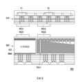
以下請參照圖2,圖2繪示本發明實施例的記憶體裝置的立體結構的示意圖。記憶體裝置200包括第一晶片210以及第二晶片220。第一晶片210包括電路區塊211-1~211-N以及電路區塊212-1~212-N。第二晶片220則包括電路區塊221-1~221-N以及電路區塊222-1~222-N。其中,在第一晶片210中,各個電路區塊212-1~212-N用以設置感測放大器以及相對應的頁緩衝器。各個電路區塊211-1~211-N則用以設置相對應的位元線開關組以及源極線開關組。在第二晶片220中,各個電路區塊221-1~221-N用以設置X位址感測器,各個電路區塊222-1~222-N則用以以設置對應X位址感測器的記憶胞區塊。在本實施例中,用以設置記憶胞區塊的電路區塊222-1~222-N分別堆疊在用以設置X位址感測器的電路區塊221-1~221-N的上方。Please refer to FIG. 2 below, which is a schematic diagram of the three-dimensional structure of the memory device of the embodiment of the present invention. The
在另一方面,以電路區塊222-1為範例,在電路區塊222-1中的記憶胞區塊上,具有多條區域位元線LBL以及區域源極線LSL。各區域位元線LBL以及各區域源極線LSL相互交錯配置,且區域位元線LBL以及區域源極線LSL彼此相互平行。在各區域位元線LBL以及各區域源極線LSL上可分別形成多個焊墊。第二晶片220可透過這些焊墊來與第一晶片210上的多個焊墊相互電性耦接,並使記憶胞區塊上的區域位元線LBL以及區域源極線LSL可分別與對應的位元線開關組以及源極線開關組相互電性耦接。On the other hand, taking the circuit block 222-1 as an example, a plurality of regional bit lines LBL and regional source lines LSL are provided on the memory cell block in the circuit block 222-1. The regional bit lines LBL and the regional source lines LSL are arranged in an interlaced manner, and the regional bit lines LBL and the regional source lines LSL are parallel to each other. A plurality of pads can be formed on each regional bit line LBL and each regional source line LSL, respectively. The
在本實施例中,第一晶片210與第二晶片220透過垂直的方向上下相互貼合來完成電性耦接。在這樣的狀態下,各個電路區塊212-1~212-N中的感測放大器以及相對應的頁緩衝器可堆疊在相對應的各個電路區塊221-1~221-N的記憶胞區塊上方,各個電路區塊211-1~211-N中的位元線開關組以及源極線開關組也可堆疊在相對應的各個電路區塊221-1~221-N的記憶胞區塊上方。In this embodiment, the
在本實施例中,各個記憶胞區塊都有各自對應的感測放大器,並且以垂直向的方向相互堆疊。如此一來,完成記憶胞區塊與對應的感測放大器的電性連接的共同位元線的長度可以有效的被縮短,大幅降低記憶胞區塊與對應的感測放大器間的信號傳輸電阻,提升記憶體裝置200的工作效益。In this embodiment, each memory cell block has its own corresponding sense amplifier and is stacked vertically. In this way, the length of the common bit line that completes the electrical connection between the memory cell block and the corresponding sense amplifier can be effectively shortened, greatly reducing the signal transmission resistance between the memory cell block and the corresponding sense amplifier, thereby improving the working efficiency of the
以下請參照圖3,圖3繪示本發明實施例的記憶體裝的焊墊的結構的立體示意圖。在圖3中,以第二晶片為範例。在第二晶片中,記憶胞區塊310上可設置多條的區域位元線LBL0~LBL3以及多條的區域源極線LSL0~LSL3。其中,區域位元線LBL0~LBL3以及區域源極線LSL0~LSL3分別相互交錯配置。區域位元線LBL0~LBL3以及區域源極線LSL0~LSL3可具有相同的尺寸,並且,相鄰的各區域位元線LBL0~LBL3以及各區域源極線LSL0~LSL3間可具有相同的間距。如此一來,各區域位元線LBL0~LBL3以及各區域源極線LSL0~LSL3間所形成的寄生電容(例如電容C1、C2),可以具有實質上相同的電容值(基於製程上的誤差,寄生電容間還是會存在些許的差異)。藉此,可維持區域位元線LBL0~LBL3以及區域源極線LSL0~LSL3上的資料傳輸的品質。Please refer to FIG. 3 below, which is a three-dimensional schematic diagram of the structure of the pad of the memory device of the embodiment of the present invention. In FIG. 3, the second chip is taken as an example. In the second chip, a plurality of regional bit lines LBL0~LBL3 and a plurality of regional source lines LSL0~LSL3 can be set on the
在本實施例中,區域位元線LBL0~LBL3以及區域源極線LSL0~LSL3可透過上金屬層第一層(TM1)來形成。In this embodiment, the regional bit lines LBL0-LBL3 and the regional source lines LSL0-LSL3 may be formed through the first upper metal layer (TM1).
在另一方面,在對應區域位元線LBL0~LBL3以及區域源極線LSL0~LSL3上方的位置,可設置多個焊墊PD。多個焊墊PD分別透過多個導電通孔TV1與對應的區域位元線LBL0~LBL3以及區域源極線LSL0~LSL3相互電性耦接。焊墊PD可規律的設置在區域位元線LBL0~LBL3以及區域源極線LSL0~LSL3上方,其中相鄰的各區域位元線LBL0~LBL3以及各區域源極線LSL0~LSL3對應的兩焊墊PD間,其水平方向以及垂直方向的距離,可以都是固定的。On the other hand, a plurality of pads PD may be disposed above the corresponding regional bit lines LBL0-LBL3 and the regional source lines LSL0-LSL3. The plurality of pads PD are electrically coupled to the corresponding regional bit lines LBL0-LBL3 and the regional source lines LSL0-LSL3 through a plurality of conductive vias TV1. The pads PD may be regularly disposed above the regional bit lines LBL0-LBL3 and the regional source lines LSL0-LSL3, wherein the distances in the horizontal and vertical directions between the two pads PD corresponding to the adjacent regional bit lines LBL0-LBL3 and the regional source lines LSL0-LSL3 may be fixed.
在本實施例中,焊墊PD例如可以透過上金屬層第二層(TM2)來形成。In this embodiment, the pad PD may be formed, for example, through the upper metal layer second layer (TM2).
值得一提的,關於第一晶片上的焊墊的設置方式,也可根據圖3的實施方式進行設置,在此不多贅述。It is worth mentioning that the arrangement of the bonding pads on the first chip can also be arranged according to the implementation method of FIG3 , which will not be elaborated herein.
以下請參照圖4,圖4繪示本發明實施例的記憶體裝的焊墊的俯視示意圖。在圖4中,多條的區域位元線LBL0~LBLN以及多條的區域源極線LSL0~LSLN交錯平行設置,並可覆蓋記憶包區塊(未繪示)。區域位元線LBL0~LBLN以及區域源極線LSL0~LSLN可具有相同的尺寸,且相鄰的各區域位元線LBL0~LBLN以及各區域源極線LSL0~LSLN間距有相同的間距,並形成實質上具有相同電容值的寄生電容。Please refer to FIG. 4 below, which is a schematic top view of a pad of a memory device according to an embodiment of the present invention. In FIG. 4, a plurality of regional bit lines LBL0~LBLN and a plurality of regional source lines LSL0~LSLN are arranged in parallel and staggered, and may cover a memory package block (not shown). The regional bit lines LBL0~LBLN and the regional source lines LSL0~LSLN may have the same size, and the adjacent regional bit lines LBL0~LBLN and the adjacent regional source lines LSL0~LSLN may have the same spacing, and form parasitic capacitors having substantially the same capacitance value.
多個焊墊PD分別設置在區域位元線LBL0~LBLN以及區域源極線LSL0~LSLN上方,並透過導電通孔,分別與區域位元線LBL0~LBLN以及區域源極線LSL0~LSLN電性連接。A plurality of bonding pads PD are respectively disposed above the regional bit lines LBL0~LBLN and the regional source lines LSL0~LSLN, and are respectively electrically connected to the regional bit lines LBL0~LBLN and the regional source lines LSL0~LSLN through conductive vias.
以下請參照圖5,圖5繪示本發明實施例的記憶體裝置的電路示意圖。在圖5中,記憶體裝置500包括第一晶片510以及第二晶片520。第一晶片510中具有感測放大器SA1、SA2、頁緩衝器PB1、PB2、多個位元線開關BLT1、BLT2以及多個源極線開關SLT1、SLT2。其中,感測放大器SA1耦接至頁緩衝器PB1,並耦接至位元線開關BLT1。感測放大器SA2則耦接至頁緩衝器PB2,並耦接至位元線開關BLT2。多個源極線開關SLT1、SLT2未耦接至第一晶片510的端點,可耦接至接地端以接收參考接地電壓GND。Please refer to FIG. 5 below, which shows a circuit diagram of a memory device of an embodiment of the present invention. In FIG. 5, the
第二晶片520包括多個記憶胞區塊521、522。以記憶胞區塊521為範例,記憶胞區塊521具有多條區域位元線LBL0~LBL3以及多條區域源極線LSL0~LSL3。在本實施例中,區域位元線LBL0~LBL3分別透過多個連接結構PDA以耦接至不同的位元線開關BLT1,區域源極線LSL0~LSL3同樣分別透過多個連接結構PDA以耦接至不同的源極線開關SLT1。其中,每一個連接結構PDA為第一晶片510以及第二晶片520上相互耦接的二焊墊。The
附帶一提的,記憶胞區塊521、522可包括三維堆疊的及式(AND)或反或式(NOR)快閃記憶胞陣列。Incidentally, the
在本實施例中,感測放大器SA1、SA2可應用本領域通常知識者所熟知的,應用於記憶體的,任意的感測放大電路來實施。頁緩衝器PB1、PB2可以為數位電路,並可應用本領域通常知識者所熟知的,應用於記憶體的,任意的頁緩衝電路,沒有一定的限制。In this embodiment, the sense amplifiers SA1 and SA2 can be implemented by any sense amplifier circuit known to those skilled in the art and applied to memory. The page buffers PB1 and PB2 can be digital circuits and can be implemented by any page buffer circuit known to those skilled in the art and applied to memory without any limitation.
請參照圖6,圖6繪示本發明一實施例的記憶體裝置的剖面結構的示意圖。記憶體裝置600包括第一晶片610以及第二晶片620。第一晶片610中具有多個感測放大器、多個位元線開關、多個源極線開關以及多個頁緩衝器。在圖6中,第一晶片610中具有電晶體T1、T2。電晶體T1、T2用以建構位元線開關、源極線開關或其他控制電路。其中,電晶體T1的一端(其源極或汲極)可耦接至焊墊PD11,電晶體T2的一端(其源極或汲極)則可耦接至焊墊PD12。Please refer to FIG6 , which is a schematic diagram of a cross-sectional structure of a memory device of an embodiment of the present invention. The
在另一方面,第二晶片620中具有記憶胞區621。記憶胞區621中可具有多個記憶胞區塊。記憶胞區塊的區域位元線或區域源極線可耦接至焊墊PD21。其中,焊墊PD21可與相對的焊墊PD11相互電性耦接,並使第一晶片610中,作為源極線開關或位元線開關的電晶體T1,可以與第二晶片620中,區域源極線或區域位元線相互連接。On the other hand, the
附帶一提的,第二晶片520中可更包括直通矽晶穿孔TAV1。其中直通矽晶穿孔TAV1的一端耦接至第二晶片620的底金屬層BM4,並穿透第二晶片520中的字元線區,以連接至焊墊PD22。其中,焊墊PD22可與相對的焊墊PD12相互電性耦接,並使第一晶片610中的電晶體T2可與第二晶片620間進行信號的傳輸動作。Incidentally, the
附帶一提的,在本實施例中,在底金屬層BM4下方,可設置X位址解碼器。X位址解碼器可進行位置解碼動作,並提供存取位址資訊至記憶胞區621。Incidentally, in this embodiment, an X address decoder may be disposed below the bottom metal layer BM4 . The X address decoder may perform position decoding and provide access address information to the
以下請參照圖7至圖9,圖7至圖9繪示本發明實施例的記憶體裝置的周邊電路的連接方式的架構示意圖。在本發明實施例中,記憶體裝置的第一晶片中更包括周邊電路。周邊電路可與外部電子裝置進行信號傳輸動作,並進行相關於記憶體裝置存取動作的多個控制動作。Please refer to FIG. 7 to FIG. 9 below, which are schematic diagrams showing the connection method of the peripheral circuit of the memory device of the embodiment of the present invention. In the embodiment of the present invention, the first chip of the memory device further includes a peripheral circuit. The peripheral circuit can perform signal transmission operations with an external electronic device and perform multiple control operations related to the access operation of the memory device.
在本實施例中,周邊電路可耦接至多個直通矽晶穿孔,並透過直通矽晶穿孔以與外部電子裝置進行多個控制信號以及電源信號的傳收動作。上述的直通矽晶穿孔形成在第二晶片中,並穿透第二晶片以與第一晶片中的周邊電路相互電性連接。In this embodiment, the peripheral circuit can be coupled to a plurality of through-silicon vias and transmit and receive a plurality of control signals and power signals with an external electronic device through the through-silicon vias. The above-mentioned through-silicon vias are formed in the second chip and penetrate the second chip to be electrically connected to the peripheral circuit in the first chip.
在圖7的立體圖中,在第二晶片中的周邊區域上的接地多晶矽(ground poly)層710上,可透過蝕刻動作來在使接地多晶矽層710產生多個分隔島711。這些分隔島711彼此相互物理性隔離。另外,在第二晶片中,可在分隔島711上產生多個直通矽晶穿孔TSV。基於分隔島711彼此間相互物理性隔離,且與接地多晶矽層710相互物理性隔離,直通矽晶穿孔TSV彼此間可產生相互電性隔離的效果。In the perspective view of FIG. 7 , a plurality of
在圖8的剖面圖中,直通矽晶穿孔TSV穿透分隔島711,並耦接在焊墊PD2以及導電凸塊MB間。導電凸塊MB形成在第二晶片的第二表面S2,焊墊PD2則形成在第二晶片的第一表面S1上,其中第一表面S1與第二表面S2相對。值得注意的,在穿透第二晶片時,直通矽晶穿孔TSV穿過第二晶片的無電路區域Z1,以避免與第二晶片的內部電路產生信號傳輸上的衝突。In the cross-sectional view of FIG8 , the through-silicon via TSV penetrates the
此外,焊墊PD2用以與第一晶片上的焊墊PD1電性耦接。第一晶片上的焊墊PD1則可電性耦接至第一晶片中的周邊電路。如此一來,外部電子裝置可透過導電凸塊MB,藉由直通矽晶穿孔TSV、焊墊PD2、PD1所形成的信號傳輸路徑,來與第一晶片的周邊電路進行信號傳輸動作。In addition, the pad PD2 is used to electrically couple with the pad PD1 on the first chip. The pad PD1 on the first chip can be electrically coupled to the peripheral circuit in the first chip. In this way, the external electronic device can transmit signals with the peripheral circuit of the first chip through the conductive bump MB through the signal transmission path formed by the through-silicon via TSV, the pad PD2, and the PD1.
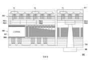
根據圖9的記憶體裝置的剖面示意圖可以得知,記憶體裝置900中,第一晶片910具有周邊電路區911以及以外的非周邊電路區。周邊電路區911用以設置周邊電路,非周邊電路區用以設置感測放大器、頁緩衝器、源極線開關以及位元線開關。第一晶片910上具有焊墊PD11、PD12以及PD13。第二晶片920具有記憶胞區921。記憶胞區921中具有多個記憶胞區塊。第二晶片920相對於第一晶片910的表面上並具有焊墊PD21、PD22以及PD23。其中第二晶片920上的焊墊PD21、PD22以及PD23分別與第一晶片910上的焊墊PD11、PD12以及PD13相互電性耦接。According to the cross-sectional schematic diagram of the memory device in FIG9 , in the
其中,焊墊PD11用以連接至第一晶片910中的位元線開關或源極線開關,焊墊PD21用以連接至第二晶片920中,記憶胞區塊的區域位元線或區域源極線。焊墊PD12可連接至第一晶片910中的任意電晶體,焊墊PD22可連接至第二晶片920中的任意金屬層。焊墊PD13可連接至第一晶片910中的周邊電路,焊墊PD23則可連接至形成在第二晶片910中的直通矽晶穿孔TSV。直通矽晶穿孔TSV穿透第二晶片920,並耦接形成在第二晶片920另一表面上的導電凸塊MB。Among them, pad PD11 is used to connect to the bit line switch or source line switch in the
請參照圖10,圖10繪示本發明實施例的記憶體裝置的立體架構的示意圖。記憶體裝置1000包括第一晶片1110以及第二晶片1120。第一晶片1110覆蓋在第二晶片上1120。第一晶片1110具有周邊電路區1111以及非周邊電路區1112~1115。周邊電路區1111用以設置周邊電路。非周邊電路區1112~1115用以設置感測放大器、頁緩衝器、源極線開關以及位元線開關。Please refer to FIG. 10, which is a schematic diagram of a three-dimensional structure of a memory device according to an embodiment of the present invention. The
第一晶片1110覆蓋在記憶胞區1121的區域上,透過多個焊墊以與第二晶片1120上的多個焊墊相互電性耦接。周邊電路並透過焊墊PDP以與第二晶片1120中的多個直通矽晶穿孔TSV電性耦接。其中,直通矽晶穿孔TSV可穿透第二晶片1120中的多晶矽接地層上所形成的多個分隔島1123。The
綜上所述,本發明的記憶體裝置使感測放大器、頁緩衝器、源極線開關以及位元線開關設置在第一晶片中,使記憶胞區塊設置在第二晶片中。第一晶片、第二晶片上並分別形成多個焊墊,透過使第一晶片與第二晶片上的焊墊相互電性耦接以形成完整的記憶體裝置。據此,記憶體裝置中,各個記憶胞區塊具有各自對應的感測放大器。並且,感測放大器可透過焊墊連接至對應的記憶胞區塊,其間的傳輸導線的長度可以有效被減短,降低信號傳輸阻抗,並提升記憶體裝置的工作效益。In summary, the memory device of the present invention has a sense amplifier, a page buffer, a source line switch, and a bit line switch disposed in a first chip, and a memory cell block disposed in a second chip. A plurality of pads are formed on the first chip and the second chip, respectively, and a complete memory device is formed by electrically coupling the pads on the first chip and the second chip. Accordingly, in the memory device, each memory cell block has its own corresponding sense amplifier. Furthermore, the sense amplifier can be connected to the corresponding memory cell block through the pad, and the length of the transmission wire therebetween can be effectively shortened, thereby reducing the signal transmission impedance and improving the working efficiency of the memory device.
100、200、500、600、900、1000:記憶體裝置 110、210、510、610、910、1110:第一晶片 1112~1115:非周邊電路區 1121:記憶胞區 120、220、520、620、920、1120:第二晶片 211-1~222-N:電路區塊 310:記憶胞區塊 621:記憶胞區 710:接地多晶矽層 711、1123:分隔島 911、1111:周邊電路區 BLT1、BLT2:位元線開關 BM4:底金屬層 C1、C2:電容 GND:參考接地電壓 LBL、LBL0~LBL3:區域位元線 LSL、LSL0~LSL3:區域源極線 MB:導電凸塊 PB1、PB2:頁緩衝器 PD1、PD2、PD11~PD23、PDP:焊墊 PDA:連接結構 S1、S2:表面 SA1、SA2:感測放大器 SLT1、SLT2:源極線開關 T1、T2:電晶體 TAV1、TSV:直通矽晶穿孔 TM2:上金屬層 Z1:無電路區域100, 200, 500, 600, 900, 1000:
圖1繪示本發明一實施例的記憶體裝置的示意圖。 圖2繪示本發明實施例的記憶體裝置的立體結構的示意圖。 圖3繪示本發明實施例的記憶體裝的焊墊的結構的立體示意圖。 圖4繪示本發明實施例的記憶體裝的焊墊的俯視示意圖。 圖5繪示本發明實施例的記憶體裝置的電路示意圖。 圖6繪示本發明一實施例的記憶體裝置的剖面結構的示意圖。 圖7至圖9繪示本發明實施例的記憶體裝置的周邊電路的連接方式的架構示意圖。 圖10繪示本發明實施例的記憶體裝置的立體架構的示意圖。FIG. 1 is a schematic diagram of a memory device according to an embodiment of the present invention.FIG. 2 is a schematic diagram of a three-dimensional structure of a memory device according to an embodiment of the present invention.FIG. 3 is a three-dimensional schematic diagram of the structure of a pad of a memory device according to an embodiment of the present invention.FIG. 4 is a top view schematic diagram of a pad of a memory device according to an embodiment of the present invention.FIG. 5 is a circuit schematic diagram of a memory device according to an embodiment of the present invention.FIG. 6 is a schematic diagram of a cross-sectional structure of a memory device according to an embodiment of the present invention.FIG. 7 to FIG. 9 are schematic diagrams of the connection method of the peripheral circuit of a memory device according to an embodiment of the present invention.FIG. 10 is a schematic diagram of the three-dimensional structure of a memory device according to an embodiment of the present invention.
100:記憶體裝置100: Memory device
110:第一晶片110: First chip
120:第二晶片120: Second chip
PD1、PD2:焊墊PD1, PD2: solder pads
S1:表面S1: Surface
Claims (13)
Translated fromChinesePriority Applications (1)
| Application Number | Priority Date | Filing Date | Title |
|---|---|---|---|
| TW112117084ATWI841377B (en) | 2023-05-09 | 2023-05-09 | Memory device |
Applications Claiming Priority (1)
| Application Number | Priority Date | Filing Date | Title |
|---|---|---|---|
| TW112117084ATWI841377B (en) | 2023-05-09 | 2023-05-09 | Memory device |
Publications (2)
| Publication Number | Publication Date |
|---|---|
| TWI841377Btrue TWI841377B (en) | 2024-05-01 |
| TW202446221A TW202446221A (en) | 2024-11-16 |
Family
ID=92077000
Family Applications (1)
| Application Number | Title | Priority Date | Filing Date |
|---|---|---|---|
| TW112117084ATWI841377B (en) | 2023-05-09 | 2023-05-09 | Memory device |
Country Status (1)
| Country | Link |
|---|---|
| TW (1) | TWI841377B (en) |
Citations (5)
| Publication number | Priority date | Publication date | Assignee | Title |
|---|---|---|---|---|
| TW201232547A (en)* | 2011-01-19 | 2012-08-01 | Macronix Int Co Ltd | Architecture for 3D memory array |
| TW202115737A (en)* | 2019-10-14 | 2021-04-16 | 大陸商長江存儲科技有限責任公司 | Cell current measurement method for three-dimensional memory |
| US20220181283A1 (en)* | 2020-12-07 | 2022-06-09 | Sandisk Technologies Llc | Memory die with source side of three-dimensional memory array bonded to logic die and methods of making the same |
| US20220399362A1 (en)* | 2021-06-15 | 2022-12-15 | Sandisk Technologies Llc | Three-dimensional memory array with dual-level peripheral circuits and methods for forming the same |
| US20230074030A1 (en)* | 2019-06-14 | 2023-03-09 | Kioxia Corporation | Semiconductor memory device |
- 2023
- 2023-05-09TWTW112117084Apatent/TWI841377B/enactive
Patent Citations (5)
| Publication number | Priority date | Publication date | Assignee | Title |
|---|---|---|---|---|
| TW201232547A (en)* | 2011-01-19 | 2012-08-01 | Macronix Int Co Ltd | Architecture for 3D memory array |
| US20230074030A1 (en)* | 2019-06-14 | 2023-03-09 | Kioxia Corporation | Semiconductor memory device |
| TW202115737A (en)* | 2019-10-14 | 2021-04-16 | 大陸商長江存儲科技有限責任公司 | Cell current measurement method for three-dimensional memory |
| US20220181283A1 (en)* | 2020-12-07 | 2022-06-09 | Sandisk Technologies Llc | Memory die with source side of three-dimensional memory array bonded to logic die and methods of making the same |
| US20220399362A1 (en)* | 2021-06-15 | 2022-12-15 | Sandisk Technologies Llc | Three-dimensional memory array with dual-level peripheral circuits and methods for forming the same |
Also Published As
| Publication number | Publication date |
|---|---|
| TW202446221A (en) | 2024-11-16 |
Similar Documents
| Publication | Publication Date | Title |
|---|---|---|
| US9070569B2 (en) | Semiconductor memory devices and semiconductor packages | |
| US20180331074A1 (en) | Microelectronic Package Having Stub Minimization Using Symmetrically-Positioned Duplicate Sets of Terminals for Wirebond Assemblies Without Windows | |
| US8633596B2 (en) | Semiconductor package with bonding wires of reduced loop inductance | |
| US20170092615A1 (en) | Semiconductor memory device | |
| US11881279B2 (en) | Solid state drive device and method for fabricating solid state drive device | |
| US20200402959A1 (en) | Stacked semiconductor package having an interposer | |
| JP2647023B2 (en) | Semiconductor storage device | |
| TWI867174B (en) | Semiconductor package | |
| US20250210514A1 (en) | Semiconductor module | |
| CN106898603A (en) | High-speed semiconductor module | |
| TWI841377B (en) | Memory device | |
| US6956783B2 (en) | Semiconductor memory device including fuse element | |
| JP7611962B2 (en) | Memory Devices | |
| US20240213219A1 (en) | Memory stack structure including power distribution structures and a high-bandwidth memory including the memory stack structure | |
| TW202324672A (en) | Semiconductor devices including stacked dies with interleaved wire bonds and associated systems and methods | |
| US20070090500A1 (en) | Housed DRAM chip for high-speed applications | |
| CN116367540B (en) | Semiconductor structure and forming method thereof | |
| US20250015051A1 (en) | Semiconductor package having memory devices stacked in staircase | |
| US20250183238A1 (en) | Stack chip package | |
| US20250024690A1 (en) | Memory chip and semiconductor package including the same | |
| US20240347524A1 (en) | Semiconductor package | |
| US20250056806A1 (en) | Semiconductor device and data storage system including the same | |
| KR20240167183A (en) | Semiconductor device and semiconductor package including the same |