TWI841145B - Semiconductor device and method for manufacturing the same - Google Patents
Semiconductor device and method for manufacturing the sameDownload PDFInfo
- Publication number
- TWI841145B TWI841145BTW111149874ATW111149874ATWI841145BTW I841145 BTWI841145 BTW I841145BTW 111149874 ATW111149874 ATW 111149874ATW 111149874 ATW111149874 ATW 111149874ATW I841145 BTWI841145 BTW I841145B
- Authority
- TW
- Taiwan
- Prior art keywords
- layer
- oxide semiconductor
- electrode layer
- region
- addition
- Prior art date
Links
- 239000004065semiconductorSubstances0.000titleclaimsabstractdescription357
- 238000000034methodMethods0.000titledescription38
- 238000004519manufacturing processMethods0.000titledescription32
- 229910052751metalInorganic materials0.000claimsdescription78
- 239000002184metalSubstances0.000claimsdescription72
- 229910052733galliumInorganic materials0.000claimsdescription18
- 229910052782aluminiumInorganic materials0.000claimsdescription17
- 239000011701zincSubstances0.000claimsdescription14
- 229910052725zincInorganic materials0.000claimsdescription12
- 229910052738indiumInorganic materials0.000claimsdescription11
- HCHKCACWOHOZIP-UHFFFAOYSA-NZincChemical compound[Zn]HCHKCACWOHOZIP-UHFFFAOYSA-N0.000claimsdescription2
- 239000010408filmSubstances0.000abstractdescription243
- 239000010409thin filmSubstances0.000abstractdescription139
- 239000000872bufferSubstances0.000abstractdescription137
- 230000015572biosynthetic processEffects0.000abstractdescription53
- 238000009826distributionMethods0.000abstractdescription5
- 239000010410layerSubstances0.000description706
- 239000000758substrateSubstances0.000description97
- 229910007541Zn OInorganic materials0.000description78
- 239000010936titaniumSubstances0.000description59
- 239000000463materialSubstances0.000description58
- 229910052760oxygenInorganic materials0.000description51
- 239000004973liquid crystal related substanceSubstances0.000description48
- 239000001301oxygenSubstances0.000description48
- QVGXLLKOCUKJST-UHFFFAOYSA-Natomic oxygenChemical compound[O]QVGXLLKOCUKJST-UHFFFAOYSA-N0.000description47
- 229910052719titaniumInorganic materials0.000description46
- 238000005530etchingMethods0.000description41
- XLOMVQKBTHCTTD-UHFFFAOYSA-NZinc monoxideChemical compound[Zn]=OXLOMVQKBTHCTTD-UHFFFAOYSA-N0.000description40
- RTAQQCXQSZGOHL-UHFFFAOYSA-NTitaniumChemical compound[Ti]RTAQQCXQSZGOHL-UHFFFAOYSA-N0.000description39
- 238000004364calculation methodMethods0.000description39
- 238000004544sputter depositionMethods0.000description37
- 238000010586diagramMethods0.000description29
- 229910052750molybdenumInorganic materials0.000description28
- 238000010438heat treatmentMethods0.000description26
- 239000003990capacitorSubstances0.000description25
- 230000001681protective effectEffects0.000description22
- 239000011787zinc oxideSubstances0.000description22
- 230000006870functionEffects0.000description21
- 239000002245particleSubstances0.000description21
- 238000000329molecular dynamics simulationMethods0.000description20
- 239000000123paperSubstances0.000description20
- ZOKXTWBITQBERF-UHFFFAOYSA-NMolybdenumChemical compound[Mo]ZOKXTWBITQBERF-UHFFFAOYSA-N0.000description19
- 239000013078crystalSubstances0.000description19
- 239000011733molybdenumSubstances0.000description19
- PXHVJJICTQNCMI-UHFFFAOYSA-NNickelChemical compound[Ni]PXHVJJICTQNCMI-UHFFFAOYSA-N0.000description18
- 229910044991metal oxideInorganic materials0.000description18
- 150000004706metal oxidesChemical class0.000description18
- 238000005401electroluminescenceMethods0.000description17
- 238000009413insulationMethods0.000description17
- 239000011572manganeseSubstances0.000description17
- XAGFODPZIPBFFR-UHFFFAOYSA-NaluminiumChemical compound[Al]XAGFODPZIPBFFR-UHFFFAOYSA-N0.000description15
- 239000000203mixtureSubstances0.000description15
- 239000011159matrix materialSubstances0.000description14
- 125000004430oxygen atomChemical groupO*0.000description14
- 238000000206photolithographyMethods0.000description14
- PWHULOQIROXLJO-UHFFFAOYSA-NManganeseChemical compound[Mn]PWHULOQIROXLJO-UHFFFAOYSA-N0.000description13
- 125000004429atomChemical group0.000description13
- 229910052748manganeseInorganic materials0.000description13
- 239000004020conductorSubstances0.000description12
- 239000003566sealing materialSubstances0.000description12
- 238000011282treatmentMethods0.000description12
- 229910052581Si3N4Inorganic materials0.000description11
- VYPSYNLAJGMNEJ-UHFFFAOYSA-NSilicium dioxideChemical compoundO=[Si]=OVYPSYNLAJGMNEJ-UHFFFAOYSA-N0.000description11
- 239000007789gasSubstances0.000description11
- 239000003094microcapsuleSubstances0.000description11
- HQVNEWCFYHHQES-UHFFFAOYSA-Nsilicon nitrideChemical compoundN12[Si]34N5[Si]62N3[Si]51N64HQVNEWCFYHHQES-UHFFFAOYSA-N0.000description11
- 229910052814silicon oxideInorganic materials0.000description11
- XEEYBQQBJWHFJM-UHFFFAOYSA-NIronChemical compound[Fe]XEEYBQQBJWHFJM-UHFFFAOYSA-N0.000description10
- 229910052759nickelInorganic materials0.000description10
- 229920005989resinPolymers0.000description10
- 239000011347resinSubstances0.000description10
- QTBSBXVTEAMEQO-UHFFFAOYSA-NAcetic acidChemical compoundCC(O)=OQTBSBXVTEAMEQO-UHFFFAOYSA-N0.000description9
- 239000000956alloySubstances0.000description9
- 239000012298atmosphereSubstances0.000description9
- 239000003795chemical substances by applicationSubstances0.000description9
- 230000002829reductive effectEffects0.000description9
- XKRFYHLGVUSROY-UHFFFAOYSA-NArgonChemical compound[Ar]XKRFYHLGVUSROY-UHFFFAOYSA-N0.000description8
- GWEVSGVZZGPLCZ-UHFFFAOYSA-NTitan oxideChemical compoundO=[Ti]=OGWEVSGVZZGPLCZ-UHFFFAOYSA-N0.000description8
- 229910045601alloyInorganic materials0.000description8
- 238000004040coloringMethods0.000description8
- 230000005684electric fieldEffects0.000description8
- 230000036961partial effectEffects0.000description8
- 239000002356single layerSubstances0.000description8
- 239000000126substanceSubstances0.000description8
- 229910052721tungstenInorganic materials0.000description8
- 238000001039wet etchingMethods0.000description8
- XUIMIQQOPSSXEZ-UHFFFAOYSA-NSiliconChemical compound[Si]XUIMIQQOPSSXEZ-UHFFFAOYSA-N0.000description7
- 150000001875compoundsChemical class0.000description7
- 229910003437indium oxideInorganic materials0.000description7
- PJXISJQVUVHSOJ-UHFFFAOYSA-Nindium(iii) oxideChemical compound[O-2].[O-2].[O-2].[In+3].[In+3]PJXISJQVUVHSOJ-UHFFFAOYSA-N0.000description7
- WPBNNNQJVZRUHP-UHFFFAOYSA-Lmanganese(2+);methyl n-[[2-(methoxycarbonylcarbamothioylamino)phenyl]carbamothioyl]carbamate;n-[2-(sulfidocarbothioylamino)ethyl]carbamodithioateChemical compound[Mn+2].[S-]C(=S)NCCNC([S-])=S.COC(=O)NC(=S)NC1=CC=CC=C1NC(=S)NC(=O)OCWPBNNNQJVZRUHP-UHFFFAOYSA-L0.000description7
- 230000003647oxidationEffects0.000description7
- 238000007254oxidation reactionMethods0.000description7
- 239000010703siliconSubstances0.000description7
- 229910052710siliconInorganic materials0.000description7
- OGIDPMRJRNCKJF-UHFFFAOYSA-Ntitanium oxideInorganic materials[Ti]=OOGIDPMRJRNCKJF-UHFFFAOYSA-N0.000description7
- 229910052723transition metalInorganic materials0.000description7
- IJGRMHOSHXDMSA-UHFFFAOYSA-NAtomic nitrogenChemical compoundN#NIJGRMHOSHXDMSA-UHFFFAOYSA-N0.000description6
- NBIIXXVUZAFLBC-UHFFFAOYSA-NPhosphoric acidChemical compoundOP(O)(O)=ONBIIXXVUZAFLBC-UHFFFAOYSA-N0.000description6
- 239000010949copperSubstances0.000description6
- 230000000694effectsEffects0.000description6
- 238000005516engineering processMethods0.000description6
- 239000012535impuritySubstances0.000description6
- AMGQUBHHOARCQH-UHFFFAOYSA-Nindium;oxotinChemical compound[In].[Sn]=OAMGQUBHHOARCQH-UHFFFAOYSA-N0.000description6
- 238000003780insertionMethods0.000description6
- 230000037431insertionEffects0.000description6
- 229910052742ironInorganic materials0.000description6
- 239000007788liquidSubstances0.000description6
- 239000000243solutionSubstances0.000description6
- 239000012798spherical particleSubstances0.000description6
- 239000010937tungstenSubstances0.000description6
- RYGMFSIKBFXOCR-UHFFFAOYSA-NCopperChemical compound[Cu]RYGMFSIKBFXOCR-UHFFFAOYSA-N0.000description5
- 206010021143HypoxiaDiseases0.000description5
- 239000000969carrierSubstances0.000description5
- 239000000460chlorineSubstances0.000description5
- 239000011651chromiumSubstances0.000description5
- 238000004891communicationMethods0.000description5
- 229910052802copperInorganic materials0.000description5
- 239000000945fillerSubstances0.000description5
- 239000011521glassSubstances0.000description5
- 239000012299nitrogen atmosphereSubstances0.000description5
- QGLKJKCYBOYXKC-UHFFFAOYSA-NnonaoxidotritungstenChemical compoundO=[W]1(=O)O[W](=O)(=O)O[W](=O)(=O)O1QGLKJKCYBOYXKC-UHFFFAOYSA-N0.000description5
- 230000003287optical effectEffects0.000description5
- 238000009832plasma treatmentMethods0.000description5
- 230000002441reversible effectEffects0.000description5
- 238000003860storageMethods0.000description5
- 229910052715tantalumInorganic materials0.000description5
- WFKWXMTUELFFGS-UHFFFAOYSA-NtungstenChemical compound[W]WFKWXMTUELFFGS-UHFFFAOYSA-N0.000description5
- 229910001930tungsten oxideInorganic materials0.000description5
- QGZKDVFQNNGYKY-UHFFFAOYSA-NAmmoniaChemical compoundNQGZKDVFQNNGYKY-UHFFFAOYSA-N0.000description4
- MHAJPDPJQMAIIY-UHFFFAOYSA-NHydrogen peroxideChemical compoundOOMHAJPDPJQMAIIY-UHFFFAOYSA-N0.000description4
- 229910052786argonInorganic materials0.000description4
- 239000012300argon atmosphereSubstances0.000description4
- HVYWMOMLDIMFJA-DPAQBDIFSA-NcholesterolChemical compoundC1C=C2C[C@@H](O)CC[C@]2(C)[C@@H]2[C@@H]1[C@@H]1CC[C@H]([C@H](C)CCCC(C)C)[C@@]1(C)CC2HVYWMOMLDIMFJA-DPAQBDIFSA-N0.000description4
- 229910052804chromiumInorganic materials0.000description4
- 239000010941cobaltSubstances0.000description4
- 229910017052cobaltInorganic materials0.000description4
- GUTLYIVDDKVIGB-UHFFFAOYSA-Ncobalt atomChemical compound[Co]GUTLYIVDDKVIGB-UHFFFAOYSA-N0.000description4
- KPUWHANPEXNPJT-UHFFFAOYSA-NdisiloxaneChemical class[SiH3]O[SiH3]KPUWHANPEXNPJT-UHFFFAOYSA-N0.000description4
- 238000001312dry etchingMethods0.000description4
- 230000007246mechanismEffects0.000description4
- 229920003023plasticPolymers0.000description4
- 239000004033plasticSubstances0.000description4
- 238000003786synthesis reactionMethods0.000description4
- -1tungsten nitrideChemical class0.000description4
- YVTHLONGBIQYBO-UHFFFAOYSA-Nzinc indium(3+) oxygen(2-)Chemical compound[O--].[Zn++].[In+3]YVTHLONGBIQYBO-UHFFFAOYSA-N0.000description4
- ZSLUVFAKFWKJRC-IGMARMGPSA-N232ThChemical compound[232Th]ZSLUVFAKFWKJRC-IGMARMGPSA-N0.000description3
- 229910000838Al alloyInorganic materials0.000description3
- ZAMOUSCENKQFHK-UHFFFAOYSA-NChlorine atomChemical compound[Cl]ZAMOUSCENKQFHK-UHFFFAOYSA-N0.000description3
- 229910052685CuriumInorganic materials0.000description3
- 229910005191Ga 2 O 3Inorganic materials0.000description3
- GYHNNYVSQQEPJS-UHFFFAOYSA-NGalliumChemical compound[Ga]GYHNNYVSQQEPJS-UHFFFAOYSA-N0.000description3
- FYYHWMGAXLPEAU-UHFFFAOYSA-NMagnesiumChemical compound[Mg]FYYHWMGAXLPEAU-UHFFFAOYSA-N0.000description3
- GRYLNZFGIOXLOG-UHFFFAOYSA-NNitric acidChemical compoundO[N+]([O-])=OGRYLNZFGIOXLOG-UHFFFAOYSA-N0.000description3
- 229910020923Sn-OInorganic materials0.000description3
- 229910052776ThoriumInorganic materials0.000description3
- NRTOMJZYCJJWKI-UHFFFAOYSA-NTitanium nitrideChemical compound[Ti]#NNRTOMJZYCJJWKI-UHFFFAOYSA-N0.000description3
- QCWXUUIWCKQGHC-UHFFFAOYSA-NZirconiumChemical compound[Zr]QCWXUUIWCKQGHC-UHFFFAOYSA-N0.000description3
- 230000009471actionEffects0.000description3
- 229910000147aluminium phosphateInorganic materials0.000description3
- SWXQKHHHCFXQJF-UHFFFAOYSA-Nazane;hydrogen peroxideChemical compound[NH4+].[O-]OSWXQKHHHCFXQJF-UHFFFAOYSA-N0.000description3
- 229910052801chlorineInorganic materials0.000description3
- 229920001940conductive polymerPolymers0.000description3
- 238000009792diffusion processMethods0.000description3
- 239000000428dustSubstances0.000description3
- 230000005611electricityEffects0.000description3
- 229910052749magnesiumInorganic materials0.000description3
- 239000011777magnesiumSubstances0.000description3
- 150000002739metalsChemical class0.000description3
- 229910017604nitric acidInorganic materials0.000description3
- 229910052757nitrogenInorganic materials0.000description3
- 150000002894organic compoundsChemical class0.000description3
- 230000001590oxidative effectEffects0.000description3
- TWNQGVIAIRXVLR-UHFFFAOYSA-Noxo(oxoalumanyloxy)alumaneChemical compoundO=[Al]O[Al]=OTWNQGVIAIRXVLR-UHFFFAOYSA-N0.000description3
- 238000005192partitionMethods0.000description3
- 229920006267polyester filmPolymers0.000description3
- 229920002620polyvinyl fluoridePolymers0.000description3
- 238000012545processingMethods0.000description3
- 239000007787solidSubstances0.000description3
- GUVRBAGPIYLISA-UHFFFAOYSA-Ntantalum atomChemical compound[Ta]GUVRBAGPIYLISA-UHFFFAOYSA-N0.000description3
- 150000003624transition metalsChemical class0.000description3
- XLYOFNOQVPJJNP-UHFFFAOYSA-NwaterSubstancesOXLYOFNOQVPJJNP-UHFFFAOYSA-N0.000description3
- 210000000707wristAnatomy0.000description3
- 229910052726zirconiumInorganic materials0.000description3
- WZJUBBHODHNQPW-UHFFFAOYSA-N2,4,6,8-tetramethyl-1,3,5,7,2$l^{3},4$l^{3},6$l^{3},8$l^{3}-tetraoxatetrasilocaneChemical compoundC[Si]1O[Si](C)O[Si](C)O[Si](C)O1WZJUBBHODHNQPW-UHFFFAOYSA-N0.000description2
- 229920000178Acrylic resinPolymers0.000description2
- 239000004925Acrylic resinSubstances0.000description2
- CURLTUGMZLYLDI-UHFFFAOYSA-NCarbon dioxideChemical compoundO=C=OCURLTUGMZLYLDI-UHFFFAOYSA-N0.000description2
- VYZAMTAEIAYCRO-UHFFFAOYSA-NChromiumChemical compound[Cr]VYZAMTAEIAYCRO-UHFFFAOYSA-N0.000description2
- 238000003775Density Functional TheoryMethods0.000description2
- YCKRFDGAMUMZLT-UHFFFAOYSA-NFluorine atomChemical compound[F]YCKRFDGAMUMZLT-UHFFFAOYSA-N0.000description2
- XPDWGBQVDMORPB-UHFFFAOYSA-NFluoroformChemical compoundFC(F)FXPDWGBQVDMORPB-UHFFFAOYSA-N0.000description2
- 206010052128GlareDiseases0.000description2
- VEXZGXHMUGYJMC-UHFFFAOYSA-NHydrochloric acidChemical compoundClVEXZGXHMUGYJMC-UHFFFAOYSA-N0.000description2
- 229910052779NeodymiumInorganic materials0.000description2
- 239000004642PolyimideSubstances0.000description2
- BLRPTPMANUNPDV-UHFFFAOYSA-NSilaneChemical compound[SiH4]BLRPTPMANUNPDV-UHFFFAOYSA-N0.000description2
- PPBRXRYQALVLMV-UHFFFAOYSA-NStyreneChemical compoundC=CC1=CC=CC=C1PPBRXRYQALVLMV-UHFFFAOYSA-N0.000description2
- BOTDANWDWHJENH-UHFFFAOYSA-NTetraethyl orthosilicateChemical compoundCCO[Si](OCC)(OCC)OCCBOTDANWDWHJENH-UHFFFAOYSA-N0.000description2
- NIXOWILDQLNWCW-UHFFFAOYSA-Nacrylic acid groupChemical groupC(C=C)(=O)ONIXOWILDQLNWCW-UHFFFAOYSA-N0.000description2
- 229910021529ammoniaInorganic materials0.000description2
- 230000005540biological transmissionEffects0.000description2
- 239000005380borophosphosilicate glassSubstances0.000description2
- 239000005388borosilicate glassSubstances0.000description2
- DQXBYHZEEUGOBF-UHFFFAOYSA-Nbut-3-enoic acid;etheneChemical compoundC=C.OC(=O)CC=CDQXBYHZEEUGOBF-UHFFFAOYSA-N0.000description2
- 239000012069chiral reagentSubstances0.000description2
- 235000012000cholesterolNutrition0.000description2
- PMHQVHHXPFUNSP-UHFFFAOYSA-Mcopper(1+);methylsulfanylmethane;bromideChemical compoundBr[Cu].CSCPMHQVHHXPFUNSP-UHFFFAOYSA-M0.000description2
- 239000003822epoxy resinSubstances0.000description2
- 239000005038ethylene vinyl acetateSubstances0.000description2
- 230000005281excited stateEffects0.000description2
- 230000001747exhibiting effectEffects0.000description2
- 239000005262ferroelectric liquid crystals (FLCs)Substances0.000description2
- 239000011152fibreglassSubstances0.000description2
- 239000011737fluorineSubstances0.000description2
- 229910052731fluorineInorganic materials0.000description2
- 125000001153fluoro groupChemical groupF*0.000description2
- 239000001307heliumSubstances0.000description2
- 229910052734heliumInorganic materials0.000description2
- SWQJXJOGLNCZEY-UHFFFAOYSA-Nhelium atomChemical compound[He]SWQJXJOGLNCZEY-UHFFFAOYSA-N0.000description2
- 238000002513implantationMethods0.000description2
- 238000009616inductively coupled plasmaMethods0.000description2
- 239000007769metal materialSubstances0.000description2
- QEFYFXOXNSNQGX-UHFFFAOYSA-Nneodymium atomChemical compound[Nd]QEFYFXOXNSNQGX-UHFFFAOYSA-N0.000description2
- HMMGMWAXVFQUOA-UHFFFAOYSA-NoctamethylcyclotetrasiloxaneChemical compoundC[Si]1(C)O[Si](C)(C)O[Si](C)(C)O[Si](C)(C)O1HMMGMWAXVFQUOA-UHFFFAOYSA-N0.000description2
- 125000000962organic groupChemical group0.000description2
- 239000011368organic materialSubstances0.000description2
- BPUBBGLMJRNUCC-UHFFFAOYSA-Noxygen(2-);tantalum(5+)Chemical compound[O-2].[O-2].[O-2].[O-2].[O-2].[Ta+5].[Ta+5]BPUBBGLMJRNUCC-UHFFFAOYSA-N0.000description2
- 239000005360phosphosilicate glassSubstances0.000description2
- 239000000049pigmentSubstances0.000description2
- 238000001020plasma etchingMethods0.000description2
- 229920001200poly(ethylene-vinyl acetate)Polymers0.000description2
- 229920002037poly(vinyl butyral) polymerPolymers0.000description2
- 229920000647polyepoxidePolymers0.000description2
- 229920001721polyimidePolymers0.000description2
- 229920000915polyvinyl chloridePolymers0.000description2
- 239000004800polyvinyl chlorideSubstances0.000description2
- 238000001552radio frequency sputter depositionMethods0.000description2
- 230000004044responseEffects0.000description2
- 229910000077silaneInorganic materials0.000description2
- 239000002904solventSubstances0.000description2
- 125000006850spacer groupChemical group0.000description2
- 238000005507sprayingMethods0.000description2
- 230000003068static effectEffects0.000description2
- 229910001936tantalum oxideInorganic materials0.000description2
- VZGDMQKNWNREIO-UHFFFAOYSA-NtetrachloromethaneChemical compoundClC(Cl)(Cl)ClVZGDMQKNWNREIO-UHFFFAOYSA-N0.000description2
- CZDYPVPMEAXLPK-UHFFFAOYSA-NtetramethylsilaneChemical compoundC[Si](C)(C)CCZDYPVPMEAXLPK-UHFFFAOYSA-N0.000description2
- 238000007738vacuum evaporationMethods0.000description2
- 239000002699waste materialSubstances0.000description2
- 229910017073AlLiInorganic materials0.000description1
- UGFAIRIUMAVXCW-UHFFFAOYSA-NCarbon monoxideChemical compound[O+]#[C-]UGFAIRIUMAVXCW-UHFFFAOYSA-N0.000description1
- CPELXLSAUQHCOX-UHFFFAOYSA-NHydrogen bromideChemical compoundBrCPELXLSAUQHCOX-UHFFFAOYSA-N0.000description1
- DGAQECJNVWCQMB-PUAWFVPOSA-MIlexoside XXIXChemical compoundC[C@@H]1CC[C@@]2(CC[C@@]3(C(=CC[C@H]4[C@]3(CC[C@@H]5[C@@]4(CC[C@@H](C5(C)C)OS(=O)(=O)[O-])C)C)[C@@H]2[C@]1(C)O)C)C(=O)O[C@H]6[C@@H]([C@H]([C@@H]([C@H](O6)CO)O)O)O.[Na+]DGAQECJNVWCQMB-PUAWFVPOSA-M0.000description1
- 238000004510Lennard-Jones potentialMethods0.000description1
- 239000004952PolyamideSubstances0.000description1
- 229910018503SF6Inorganic materials0.000description1
- 229910000676Si alloyInorganic materials0.000description1
- 229910002808Si–O–SiInorganic materials0.000description1
- 229910006404SnO 2Inorganic materials0.000description1
- 229910001069Ti alloyInorganic materials0.000description1
- 241000237983TrochidaeSpecies0.000description1
- 238000003848UV Light-CuringMethods0.000description1
- 206010047571Visual impairmentDiseases0.000description1
- YHMKWOWVAIPFMP-UHFFFAOYSA-N[O-2].[Fe+2].[In+3].[Zn+2]Chemical compound[O-2].[Fe+2].[In+3].[Zn+2]YHMKWOWVAIPFMP-UHFFFAOYSA-N0.000description1
- AZWHFTKIBIQKCA-UHFFFAOYSA-N[Sn+2]=O.[O-2].[In+3]Chemical compound[Sn+2]=O.[O-2].[In+3]AZWHFTKIBIQKCA-UHFFFAOYSA-N0.000description1
- 230000001133accelerationEffects0.000description1
- 125000000217alkyl groupChemical group0.000description1
- 238000000137annealingMethods0.000description1
- 125000003118aryl groupChemical group0.000description1
- 229910052788bariumInorganic materials0.000description1
- DSAJWYNOEDNPEQ-UHFFFAOYSA-Nbarium atomChemical compound[Ba]DSAJWYNOEDNPEQ-UHFFFAOYSA-N0.000description1
- 230000009286beneficial effectEffects0.000description1
- UMIVXZPTRXBADB-UHFFFAOYSA-NbenzocyclobuteneChemical compoundC1=CC=C2CCC2=C1UMIVXZPTRXBADB-UHFFFAOYSA-N0.000description1
- 239000011230binding agentSubstances0.000description1
- 239000001569carbon dioxideSubstances0.000description1
- 229910002092carbon dioxideInorganic materials0.000description1
- 239000000919ceramicSubstances0.000description1
- 230000008859changeEffects0.000description1
- 238000006243chemical reactionMethods0.000description1
- 238000004140cleaningMethods0.000description1
- 239000003086colorantSubstances0.000description1
- 229920001577copolymerPolymers0.000description1
- 230000007797corrosionEffects0.000description1
- 238000005260corrosionMethods0.000description1
- 210000002858crystal cellAnatomy0.000description1
- 238000001723curingMethods0.000description1
- 238000013461designMethods0.000description1
- 239000003989dielectric materialSubstances0.000description1
- 238000006073displacement reactionMethods0.000description1
- 239000007772electrode materialSubstances0.000description1
- 239000003344environmental pollutantSubstances0.000description1
- 239000000284extractSubstances0.000description1
- 239000004744fabricSubstances0.000description1
- 238000007667floatingMethods0.000description1
- 239000011888foilSubstances0.000description1
- 230000004313glareEffects0.000description1
- 230000005283ground stateEffects0.000description1
- 210000004247handAnatomy0.000description1
- 238000013007heat curingMethods0.000description1
- FFUAGWLWBBFQJT-UHFFFAOYSA-NhexamethyldisilazaneChemical compoundC[Si](C)(C)N[Si](C)(C)CFFUAGWLWBBFQJT-UHFFFAOYSA-N0.000description1
- 230000005525hole transportEffects0.000description1
- 239000001257hydrogenSubstances0.000description1
- 229910052739hydrogenInorganic materials0.000description1
- 125000004435hydrogen atomChemical class[H]*0.000description1
- 238000003384imaging methodMethods0.000description1
- 238000007654immersionMethods0.000description1
- APFVFJFRJDLVQX-UHFFFAOYSA-Nindium atomChemical compound[In]APFVFJFRJDLVQX-UHFFFAOYSA-N0.000description1
- 239000011261inert gasSubstances0.000description1
- 150000002484inorganic compoundsChemical class0.000description1
- 229910010272inorganic materialInorganic materials0.000description1
- 239000011810insulating materialSubstances0.000description1
- 150000002500ionsChemical class0.000description1
- 239000005001laminate filmSubstances0.000description1
- 239000000696magnetic materialSubstances0.000description1
- 230000005389magnetismEffects0.000description1
- 238000001755magnetron sputter depositionMethods0.000description1
- 230000000873masking effectEffects0.000description1
- 238000007578melt-quenching techniqueMethods0.000description1
- 229910021645metal ionInorganic materials0.000description1
- 230000004048modificationEffects0.000description1
- 238000012986modificationMethods0.000description1
- KELHQGOVULCJSG-UHFFFAOYSA-Nn,n-dimethyl-1-(5-methylfuran-2-yl)ethane-1,2-diamineChemical compoundCN(C)C(CN)C1=CC=C(C)O1KELHQGOVULCJSG-UHFFFAOYSA-N0.000description1
- QKCGXXHCELUCKW-UHFFFAOYSA-Nn-[4-[4-(dinaphthalen-2-ylamino)phenyl]phenyl]-n-naphthalen-2-ylnaphthalen-2-amineChemical compoundC1=CC=CC2=CC(N(C=3C=CC(=CC=3)C=3C=CC(=CC=3)N(C=3C=C4C=CC=CC4=CC=3)C=3C=C4C=CC=CC4=CC=3)C3=CC4=CC=CC=C4C=C3)=CC=C21QKCGXXHCELUCKW-UHFFFAOYSA-N0.000description1
- 150000004767nitridesChemical class0.000description1
- 238000007645offset printingMethods0.000description1
- 239000012788optical filmSubstances0.000description1
- 230000005693optoelectronicsEffects0.000description1
- 239000005416organic matterSubstances0.000description1
- AHLBNYSZXLDEJQ-FWEHEUNISA-NorlistatChemical compoundCCCCCCCCCCC[C@H](OC(=O)[C@H](CC(C)C)NC=O)C[C@@H]1OC(=O)[C@H]1CCCCCCAHLBNYSZXLDEJQ-FWEHEUNISA-N0.000description1
- 238000004806packaging method and processMethods0.000description1
- 238000005268plasma chemical vapour depositionMethods0.000description1
- 238000002294plasma sputter depositionMethods0.000description1
- 231100000719pollutantToxicity0.000description1
- 229920002647polyamidePolymers0.000description1
- 229920000767polyanilinePolymers0.000description1
- 229920000128polypyrrolePolymers0.000description1
- 229920001296polysiloxanePolymers0.000description1
- 229920000123polythiophenePolymers0.000description1
- 230000008569processEffects0.000description1
- 230000005855radiationEffects0.000description1
- 230000006798recombinationEffects0.000description1
- 238000005215recombinationMethods0.000description1
- 238000002310reflectometryMethods0.000description1
- 238000007650screen-printingMethods0.000description1
- 238000007789sealingMethods0.000description1
- FDNAPBUWERUEDA-UHFFFAOYSA-Nsilicon tetrachlorideChemical compoundCl[Si](Cl)(Cl)ClFDNAPBUWERUEDA-UHFFFAOYSA-N0.000description1
- 229920002050silicone resinPolymers0.000description1
- 238000004088simulationMethods0.000description1
- 239000002893slagSubstances0.000description1
- 239000011734sodiumSubstances0.000description1
- 229910052708sodiumInorganic materials0.000description1
- 238000004528spin coatingMethods0.000description1
- 238000009987spinningMethods0.000description1
- 239000010935stainless steelSubstances0.000description1
- 229910001220stainless steelInorganic materials0.000description1
- 239000007858starting materialSubstances0.000description1
- 125000001424substituent groupChemical group0.000description1
- SFZCNBIFKDRMGX-UHFFFAOYSA-Nsulfur hexafluorideChemical compoundFS(F)(F)(F)(F)FSFZCNBIFKDRMGX-UHFFFAOYSA-N0.000description1
- 229960000909sulfur hexafluorideDrugs0.000description1
- 230000001360synchronised effectEffects0.000description1
- MZLGASXMSKOWSE-UHFFFAOYSA-Ntantalum nitrideChemical compound[Ta]#NMZLGASXMSKOWSE-UHFFFAOYSA-N0.000description1
- 239000013076target substanceSubstances0.000description1
- TXEYQDLBPFQVAA-UHFFFAOYSA-NtetrafluoromethaneChemical compoundFC(F)(F)FTXEYQDLBPFQVAA-UHFFFAOYSA-N0.000description1
- XOLBLPGZBRYERU-UHFFFAOYSA-Ntin dioxideChemical compoundO=[Sn]=OXOLBLPGZBRYERU-UHFFFAOYSA-N0.000description1
- 229910001887tin oxideInorganic materials0.000description1
- 239000004408titanium dioxideSubstances0.000description1
- 230000007704transitionEffects0.000description1
- 238000002834transmittanceMethods0.000description1
- FAQYAMRNWDIXMY-UHFFFAOYSA-NtrichloroboraneChemical compoundClB(Cl)ClFAQYAMRNWDIXMY-UHFFFAOYSA-N0.000description1
- QQQSFSZALRVCSZ-UHFFFAOYSA-NtriethoxysilaneChemical compoundCCO[SiH](OCC)OCCQQQSFSZALRVCSZ-UHFFFAOYSA-N0.000description1
- GIRKRMUMWJFNRI-UHFFFAOYSA-Ntris(dimethylamino)siliconChemical compoundCN(C)[Si](N(C)C)N(C)CGIRKRMUMWJFNRI-UHFFFAOYSA-N0.000description1
- OYQCBJZGELKKPM-UHFFFAOYSA-Nzinc indium(3+) oxygen(2-)Chemical compound[O-2].[Zn+2].[O-2].[In+3]OYQCBJZGELKKPM-UHFFFAOYSA-N0.000description1
Images


Classifications
- H—ELECTRICITY
- H10—SEMICONDUCTOR DEVICES; ELECTRIC SOLID-STATE DEVICES NOT OTHERWISE PROVIDED FOR
- H10D—INORGANIC ELECTRIC SEMICONDUCTOR DEVICES
- H10D30/00—Field-effect transistors [FET]
- H10D30/01—Manufacture or treatment
- H10D30/021—Manufacture or treatment of FETs having insulated gates [IGFET]
- H10D30/031—Manufacture or treatment of FETs having insulated gates [IGFET] of thin-film transistors [TFT]
- H—ELECTRICITY
- H10—SEMICONDUCTOR DEVICES; ELECTRIC SOLID-STATE DEVICES NOT OTHERWISE PROVIDED FOR
- H10D—INORGANIC ELECTRIC SEMICONDUCTOR DEVICES
- H10D30/00—Field-effect transistors [FET]
- H10D30/60—Insulated-gate field-effect transistors [IGFET]
- H10D30/67—Thin-film transistors [TFT]
- H10D30/674—Thin-film transistors [TFT] characterised by the active materials
- H10D30/6755—Oxide semiconductors, e.g. zinc oxide, copper aluminium oxide or cadmium stannate
- H—ELECTRICITY
- H01—ELECTRIC ELEMENTS
- H01L—SEMICONDUCTOR DEVICES NOT COVERED BY CLASS H10
- H01L21/00—Processes or apparatus adapted for the manufacture or treatment of semiconductor or solid state devices or of parts thereof
- H01L21/02—Manufacture or treatment of semiconductor devices or of parts thereof
- H01L21/02104—Forming layers
- H01L21/02365—Forming inorganic semiconducting materials on a substrate
- H01L21/02518—Deposited layers
- H01L21/02521—Materials
- H01L21/02565—Oxide semiconducting materials not being Group 12/16 materials, e.g. ternary compounds
- H—ELECTRICITY
- H01—ELECTRIC ELEMENTS
- H01L—SEMICONDUCTOR DEVICES NOT COVERED BY CLASS H10
- H01L21/00—Processes or apparatus adapted for the manufacture or treatment of semiconductor or solid state devices or of parts thereof
- H01L21/02—Manufacture or treatment of semiconductor devices or of parts thereof
- H01L21/02104—Forming layers
- H01L21/02365—Forming inorganic semiconducting materials on a substrate
- H01L21/02612—Formation types
- H01L21/02617—Deposition types
- H01L21/02631—Physical deposition at reduced pressure, e.g. MBE, sputtering, evaporation
- H—ELECTRICITY
- H10—SEMICONDUCTOR DEVICES; ELECTRIC SOLID-STATE DEVICES NOT OTHERWISE PROVIDED FOR
- H10D—INORGANIC ELECTRIC SEMICONDUCTOR DEVICES
- H10D30/00—Field-effect transistors [FET]
- H10D30/60—Insulated-gate field-effect transistors [IGFET]
- H10D30/67—Thin-film transistors [TFT]
- H10D30/6704—Thin-film transistors [TFT] having supplementary regions or layers in the thin films or in the insulated bulk substrates for controlling properties of the device
- H10D30/6713—Thin-film transistors [TFT] having supplementary regions or layers in the thin films or in the insulated bulk substrates for controlling properties of the device characterised by the properties of the source or drain regions, e.g. compositions or sectional shapes
- H—ELECTRICITY
- H10—SEMICONDUCTOR DEVICES; ELECTRIC SOLID-STATE DEVICES NOT OTHERWISE PROVIDED FOR
- H10D—INORGANIC ELECTRIC SEMICONDUCTOR DEVICES
- H10D30/00—Field-effect transistors [FET]
- H10D30/60—Insulated-gate field-effect transistors [IGFET]
- H10D30/67—Thin-film transistors [TFT]
- H10D30/6729—Thin-film transistors [TFT] characterised by the electrodes
- H10D30/673—Thin-film transistors [TFT] characterised by the electrodes characterised by the shapes, relative sizes or dispositions of the gate electrodes
- H—ELECTRICITY
- H10—SEMICONDUCTOR DEVICES; ELECTRIC SOLID-STATE DEVICES NOT OTHERWISE PROVIDED FOR
- H10D—INORGANIC ELECTRIC SEMICONDUCTOR DEVICES
- H10D30/00—Field-effect transistors [FET]
- H10D30/60—Insulated-gate field-effect transistors [IGFET]
- H10D30/67—Thin-film transistors [TFT]
- H10D30/6729—Thin-film transistors [TFT] characterised by the electrodes
- H10D30/6737—Thin-film transistors [TFT] characterised by the electrodes characterised by the electrode materials
- H10D30/6739—Conductor-insulator-semiconductor electrodes
- H—ELECTRICITY
- H10—SEMICONDUCTOR DEVICES; ELECTRIC SOLID-STATE DEVICES NOT OTHERWISE PROVIDED FOR
- H10D—INORGANIC ELECTRIC SEMICONDUCTOR DEVICES
- H10D30/00—Field-effect transistors [FET]
- H10D30/60—Insulated-gate field-effect transistors [IGFET]
- H10D30/67—Thin-film transistors [TFT]
- H10D30/674—Thin-film transistors [TFT] characterised by the active materials
- H10D30/6755—Oxide semiconductors, e.g. zinc oxide, copper aluminium oxide or cadmium stannate
- H10D30/6756—Amorphous oxide semiconductors
- H—ELECTRICITY
- H10—SEMICONDUCTOR DEVICES; ELECTRIC SOLID-STATE DEVICES NOT OTHERWISE PROVIDED FOR
- H10D—INORGANIC ELECTRIC SEMICONDUCTOR DEVICES
- H10D30/00—Field-effect transistors [FET]
- H10D30/60—Insulated-gate field-effect transistors [IGFET]
- H10D30/67—Thin-film transistors [TFT]
- H10D30/6757—Thin-film transistors [TFT] characterised by the structure of the channel, e.g. transverse or longitudinal shape or doping profile
- H—ELECTRICITY
- H10—SEMICONDUCTOR DEVICES; ELECTRIC SOLID-STATE DEVICES NOT OTHERWISE PROVIDED FOR
- H10D—INORGANIC ELECTRIC SEMICONDUCTOR DEVICES
- H10D62/00—Semiconductor bodies, or regions thereof, of devices having potential barriers
- H10D62/10—Shapes, relative sizes or dispositions of the regions of the semiconductor bodies; Shapes of the semiconductor bodies
- H10D62/13—Semiconductor regions connected to electrodes carrying current to be rectified, amplified or switched, e.g. source or drain regions
- H10D62/149—Source or drain regions of field-effect devices
- H10D62/151—Source or drain regions of field-effect devices of IGFETs
- H—ELECTRICITY
- H10—SEMICONDUCTOR DEVICES; ELECTRIC SOLID-STATE DEVICES NOT OTHERWISE PROVIDED FOR
- H10D—INORGANIC ELECTRIC SEMICONDUCTOR DEVICES
- H10D62/00—Semiconductor bodies, or regions thereof, of devices having potential barriers
- H10D62/10—Shapes, relative sizes or dispositions of the regions of the semiconductor bodies; Shapes of the semiconductor bodies
- H10D62/17—Semiconductor regions connected to electrodes not carrying current to be rectified, amplified or switched, e.g. channel regions
- H10D62/213—Channel regions of field-effect devices
- H10D62/221—Channel regions of field-effect devices of FETs
- H10D62/235—Channel regions of field-effect devices of FETs of IGFETs
- H—ELECTRICITY
- H10—SEMICONDUCTOR DEVICES; ELECTRIC SOLID-STATE DEVICES NOT OTHERWISE PROVIDED FOR
- H10D—INORGANIC ELECTRIC SEMICONDUCTOR DEVICES
- H10D62/00—Semiconductor bodies, or regions thereof, of devices having potential barriers
- H10D62/80—Semiconductor bodies, or regions thereof, of devices having potential barriers characterised by the materials
- H—ELECTRICITY
- H10—SEMICONDUCTOR DEVICES; ELECTRIC SOLID-STATE DEVICES NOT OTHERWISE PROVIDED FOR
- H10D—INORGANIC ELECTRIC SEMICONDUCTOR DEVICES
- H10D64/00—Electrodes of devices having potential barriers
- H10D64/20—Electrodes characterised by their shapes, relative sizes or dispositions
- H10D64/27—Electrodes not carrying the current to be rectified, amplified, oscillated or switched, e.g. gates
- H10D64/311—Gate electrodes for field-effect devices
- H10D64/411—Gate electrodes for field-effect devices for FETs
- H10D64/511—Gate electrodes for field-effect devices for FETs for IGFETs
- H10D64/512—Disposition of the gate electrodes, e.g. buried gates
- H—ELECTRICITY
- H10—SEMICONDUCTOR DEVICES; ELECTRIC SOLID-STATE DEVICES NOT OTHERWISE PROVIDED FOR
- H10D—INORGANIC ELECTRIC SEMICONDUCTOR DEVICES
- H10D64/00—Electrodes of devices having potential barriers
- H10D64/60—Electrodes characterised by their materials
- H10D64/62—Electrodes ohmically coupled to a semiconductor
- H—ELECTRICITY
- H10—SEMICONDUCTOR DEVICES; ELECTRIC SOLID-STATE DEVICES NOT OTHERWISE PROVIDED FOR
- H10D—INORGANIC ELECTRIC SEMICONDUCTOR DEVICES
- H10D86/00—Integrated devices formed in or on insulating or conducting substrates, e.g. formed in silicon-on-insulator [SOI] substrates or on stainless steel or glass substrates
- H10D86/40—Integrated devices formed in or on insulating or conducting substrates, e.g. formed in silicon-on-insulator [SOI] substrates or on stainless steel or glass substrates characterised by multiple TFTs
- H10D86/421—Integrated devices formed in or on insulating or conducting substrates, e.g. formed in silicon-on-insulator [SOI] substrates or on stainless steel or glass substrates characterised by multiple TFTs having a particular composition, shape or crystalline structure of the active layer
- H10D86/423—Integrated devices formed in or on insulating or conducting substrates, e.g. formed in silicon-on-insulator [SOI] substrates or on stainless steel or glass substrates characterised by multiple TFTs having a particular composition, shape or crystalline structure of the active layer comprising semiconductor materials not belonging to the Group IV, e.g. InGaZnO
- H—ELECTRICITY
- H10—SEMICONDUCTOR DEVICES; ELECTRIC SOLID-STATE DEVICES NOT OTHERWISE PROVIDED FOR
- H10D—INORGANIC ELECTRIC SEMICONDUCTOR DEVICES
- H10D86/00—Integrated devices formed in or on insulating or conducting substrates, e.g. formed in silicon-on-insulator [SOI] substrates or on stainless steel or glass substrates
- H10D86/40—Integrated devices formed in or on insulating or conducting substrates, e.g. formed in silicon-on-insulator [SOI] substrates or on stainless steel or glass substrates characterised by multiple TFTs
- H10D86/60—Integrated devices formed in or on insulating or conducting substrates, e.g. formed in silicon-on-insulator [SOI] substrates or on stainless steel or glass substrates characterised by multiple TFTs wherein the TFTs are in active matrices
- H—ELECTRICITY
- H10—SEMICONDUCTOR DEVICES; ELECTRIC SOLID-STATE DEVICES NOT OTHERWISE PROVIDED FOR
- H10D—INORGANIC ELECTRIC SEMICONDUCTOR DEVICES
- H10D99/00—Subject matter not provided for in other groups of this subclass
- H—ELECTRICITY
- H01—ELECTRIC ELEMENTS
- H01L—SEMICONDUCTOR DEVICES NOT COVERED BY CLASS H10
- H01L21/00—Processes or apparatus adapted for the manufacture or treatment of semiconductor or solid state devices or of parts thereof
- H01L21/02—Manufacture or treatment of semiconductor devices or of parts thereof
- H01L21/02104—Forming layers
- H01L21/02365—Forming inorganic semiconducting materials on a substrate
- H01L21/02518—Deposited layers
- H01L21/02521—Materials
- H01L21/02551—Group 12/16 materials
- H01L21/02554—Oxides
Landscapes
- Engineering & Computer Science (AREA)
- Microelectronics & Electronic Packaging (AREA)
- Condensed Matter Physics & Semiconductors (AREA)
- General Physics & Mathematics (AREA)
- Manufacturing & Machinery (AREA)
- Computer Hardware Design (AREA)
- Physics & Mathematics (AREA)
- Power Engineering (AREA)
- Thin Film Transistor (AREA)
- Liquid Crystal (AREA)
- Electroluminescent Light Sources (AREA)
- Electrodes Of Semiconductors (AREA)
- Metal-Oxide And Bipolar Metal-Oxide Semiconductor Integrated Circuits (AREA)
- Bipolar Transistors (AREA)
Abstract
Description
Translated fromChinese本發明關於一種使用氧化物半導體製造的半導體裝置及其製造方法。The present invention relates to a semiconductor device manufactured using an oxide semiconductor and a manufacturing method thereof.
金屬氧化物的種類繁多且用途廣泛。氧化銦為較普遍的材料,其被用作液晶顯示器等所需要的透明電極材料。There are many types of metal oxides and their uses are wide-ranging. Indium oxide is a more common material, which is used as a transparent electrode material required for liquid crystal displays, etc.
在金屬氧化物中存在呈現半導體特性的金屬氧化物。作為呈現半導體特性的金屬氧化物,例如有氧化鎢、氧化錫、氧化銦、氧化鋅等,並且將這些呈現半導體特性的金屬氧化物用作通道形成區的薄膜電晶體已經是眾所周知的(參照專利檔案1至4、非專利檔案1)。Among metal oxides, there are metal oxides that exhibit semiconductor properties. Examples of metal oxides that exhibit semiconductor properties include tungsten oxide, tin oxide, indium oxide, zinc oxide, etc., and thin film transistors that use these metal oxides that exhibit semiconductor properties as channel formation regions are already well known (see
另外,已知金屬氧化物不僅有一元氧化物還有多元氧化物。例如,作為包含In、Ga及Zn的多元氧化物,具有同系物(homologous series)的InGaO3(ZnO)m(m:自然數)是周知的(參照非專利檔案2至4)。In addition, metal oxides are known to include not only single oxides but also multi-element oxides. For example, InGaO3 (ZnO)m (m: a natural number) having a homologous series is known as a multi-element oxide containing In, Ga, and Zn (see Non-Patent
並且,已經確認到可以將上述那樣的由In-Ga-Zn類氧化物構成的氧化物半導體用作薄膜電晶體的通道層(參照專利檔案5、非專利檔案5及6)。Furthermore, it has been confirmed that the oxide semiconductor composed of the above-mentioned In-Ga-Zn type oxide can be used as the channel layer of the thin film transistor (refer to
[專利檔案1]日本專利申請公開昭60-198861號公報[Patent file 1] Japanese Patent Application Publication No. 60-198861
[專利檔案2]日本專利申請公開平8-264794號公報[Patent File 2] Japanese Patent Application Publication No. 8-264794
[專利檔案3]PCT國際申請日本公表平11-505377號公報[Patent File 3] PCT International Application Japanese Publication No. 11-505377
[專利檔案4]日本專利申請公開2000-150900號公報[Patent File 4] Japanese Patent Application Publication No. 2000-150900
[專利檔案5]日本專利申請公開2004-103957號公報[Patent File 5] Japanese Patent Application Publication No. 2004-103957
[非專利檔案1]M. W. Prins, K. O. Grosse-Holz, G. Muller, J. F. M. Cillessen, J. B. Giesbers, R. P. Weening, and R. M. Wolf, "A ferroelectric transparent thin-film transistor"(透明鐵電薄膜電晶體),Appl. Phys. Lett., 17 June 1996, Vol. 68 p. 3650-3652[Non-patent file 1]MW Prins, KO Grosse-Holz, G. Muller, JFM Cillessen, JB Giesbers, RP Weening, and RM Wolf, "A ferroelectric transparent thin-film transistor",Appl. Phys. Lett. , 17 June 1996, Vol. 68 p. 3650-3652
[非專利檔案2]M. Nakamura, N. Kimizuka, and T. Mohri, "The Phase Relations in the In2O3-Ga2ZnO4-ZnO System at 1350 ℃"(In2O3-Ga2ZnO4-ZnO類在1350℃時的相位關係),J. Solid State Chem., 1991, Vol. 93, p. 298-315[Non-patent file 2] M. Nakamura, N. Kimizuka, and T. Mohri, "The Phase Relations in theIn 2O3-Ga2 ZnO4-ZnO System at 1350 ℃",J. Solid State Chem. , 1991, Vol. 93, p. 298-315
[非專利檔案3]N. Kimizuka, M. Isobe, and M. Nakamura, "Syntheses and Single-Crystal Data of Homologous Compounds, In2O3(ZnO)m(m=3, 4, and 5), InGaO3(ZnO)3, and Ga2O3(ZnO)m (m=7, 8, 9, and 16) in the In2O3-ZnGa2O4-ZnO System"(同系物的合成和單晶資料,In2O3-ZnGa2O4-ZnO類的In2O3(ZnO)m (m=3, 4, and 5), InGaO3(ZnO)3, and Ga2O3(ZnO)m (m=7, 8, 9, and 16)),J. Solid State Chem., 1995, Vol. 116, p. 170-178[Non-patent file 3] N. Kimizuka, M. Isobe, and M. Nakamura, "Syntheses and Single-Crystal Data of Homologous Compounds, In2 O3 (ZnO)m (m=3, 4, and 5), InGaO3 (ZnO)3 , and Ga2 O3 (ZnO)m (m=7, 8, 9, and 16) in the In2 O3 -ZnGa2 O4 -ZnO System" (Syntheses and Single-Crystal Data of Homologous Compounds, In2 O3 -ZnGa2 O4 -ZnO System In2 O3 (ZnO)m (m=3, 4, and 5), InGaO3 (ZnO)3 , and Ga2 O3 (ZnO)m (m=7, 8, 9, and 16)),J. Solid State Chem. , 1995, Vol. 116, p. 170-178
[非專利檔案4]中村真佐樹、君塚昇、毛利尚彥、磯部光正,"


[非專利檔案5]K. Nomura, H. Ohta, K. Ueda, T. Kamiya, M. Hirano, and H. Hosono, "Thin-film transistor fabricated in single-crystalline transparent oxide semiconductor"(由單晶透明氧化物半導體製造的薄膜電晶體),SCIENCE, 2003, Vol. 300, p. 1269-1272[Non-patent file 5] K. Nomura, H. Ohta, K. Ueda, T. Kamiya, M. Hirano, and H. Hosono, "Thin-film transistor fabricated in single-crystalline transparent oxide semiconductor",SCIENCE , 2003, Vol. 300, p. 1269-1272
[非專利檔案6]K. Nomura, H. Ohta, A. Takagi, T. Kamiya, M. Hirano, and H. Hosono, "Room-temperature fabrication of transparent flexible thin-film transistors using amorphous oxide semiconductors"(在室溫下製造使用非晶氧化物半導體的透明撓性薄膜電晶體),NATURE, 2004, Vol. 432 p. 488-492[Non-patent file 6] K. Nomura, H. Ohta, A. Takagi, T. Kamiya, M. Hirano, and H. Hosono, "Room-temperature fabrication of transparent flexible thin-film transistors using amorphous oxide semiconductors",NATURE , 2004, Vol. 432 p. 488-492
本發明的目的之一在於提供一種具有穩定電特性的薄膜電晶體的可靠性高的半導體裝置。One of the purposes of the present invention is to provide a semiconductor device having a thin film transistor with stable electrical characteristics and high reliability.
在包括作為半導體層採用氧化物半導體層的反堆疊型薄膜電晶體的半導體裝置中,在氧化物半導體層之上具有緩衝層。緩衝層與半導體層的通道形成區與源極電極層及汲極電極層接觸。緩衝層在其膜中具有電阻分佈。在緩衝層中,設置在半導體層的通道形成區上的區域的導電率低於半導體層的通道形成區的導電率,並且與源極電極層及汲極電極層接觸的區域的導電率高於半導體層的通道形成區的導電率。另外,與閘極絕緣層相比,緩衝層及半導體層的導電率高(電阻低)。具體而言,按照導電率從高到低的排列順序,其分別為緩衝層的低電阻區域(與源極電極層及汲極電極層接觸的區域)、半導體層的通道形成區、緩衝層的高電阻區域(設置在通道形成區之上的區域)、閘極絕緣層。In a semiconductor device including an anti-stacked thin film transistor using an oxide semiconductor layer as a semiconductor layer, a buffer layer is provided on the oxide semiconductor layer. The buffer layer is in contact with a channel forming region of the semiconductor layer and a source electrode layer and a drain electrode layer. The buffer layer has a resistance distribution in its film. In the buffer layer, the conductivity of a region disposed on the channel forming region of the semiconductor layer is lower than the conductivity of the channel forming region of the semiconductor layer, and the conductivity of a region in contact with the source electrode layer and the drain electrode layer is higher than the conductivity of the channel forming region of the semiconductor layer. In addition, compared with the gate insulating layer, the conductivity of the buffer layer and the semiconductor layer is high (low resistance). Specifically, in order of conductivity from high to low, they are the low resistance region of the buffer layer (the region in contact with the source electrode layer and the drain electrode layer), the channel formation region of the semiconductor layer, the high resistance region of the buffer layer (the region provided above the channel formation region), and the gate insulating layer.
緩衝層中與通道形成區接觸的區域為高電阻區域,所以薄膜電晶體的電特性穩定化,而可以防止截止電流的增加等。另一方面,因為緩衝層中的與源極電極層及汲極電極層接觸的區域為低電阻區域,所以接觸電阻低,而可以使導通電流增高。因此,可以製造具有電特性高且可靠性高的薄膜電晶體的半導體裝置。The area in the buffer layer that contacts the channel formation area is a high resistance area, so the electrical characteristics of the thin film transistor are stabilized, and the increase of the cut-off current can be prevented. On the other hand, because the area in the buffer layer that contacts the source electrode layer and the drain electrode layer is a low resistance area, the contact resistance is low, and the conduction current can be increased. Therefore, a semiconductor device with a thin film transistor having high electrical characteristics and high reliability can be manufactured.
形成緩衝層,可以使用包含鈦、鉬或錳的氧化物半導體層。當使氧化物半導體層包含鈦、鉬或錳的金屬元素時,氧化物半導體層的電阻增大。To form a buffer layer, an oxide semiconductor layer containing titanium, molybdenum or manganese can be used. When the oxide semiconductor layer contains a metal element of titanium, molybdenum or manganese, the resistance of the oxide semiconductor layer increases.
注意,在本說明書中,當形成緩衝層時使緩衝層包含鈦、鉬或錳等的元素。例如,使用包含鈦、鉬或錳的靶藉由濺射法形成緩衝層。Note that in this specification, when forming a buffer layer, the buffer layer is made to contain an element such as titanium, molybdenum, or manganese. For example, the buffer layer is formed by a sputtering method using a target containing titanium, molybdenum, or manganese.
作為用於緩衝層的氧化物半導體層,使用具有半導體特性的氧化物材料即可。例如,可以使用具有表示為InMO3(ZnO)m(m>0)的結構的氧化物半導體,特別較佳使用In-Ga-Zn-O類氧化物半導體。另外,M表示選自鎵(Ga)、鐵(Fe)、鎳(Ni)、錳(Mn)及鈷(Co)中的其中之一者金屬元素或多種金屬元素。例如,作為M,除了有包含Ga的情況之外,還有包含Ga和Ni或Ga和Fe等的Ga以外的上述金屬元素的情況。此外,在上述氧化物半導體中,有不僅包含作為M的金屬元素,而且還包含作為雜質元素的Fe、Ni等其他過渡金屬元素或該過渡金屬的氧化物的氧化物半導體。在本說明書中,在具有表示為InMO3(ZnO)m(m>0)的結構的氧化物半導體中,將具有作為M至少包含Ga的結構的氧化物半導體稱為In-Ga-Zn-O類氧化物半導體,並且將該薄膜也稱為In-Ga-Zn-O類非單晶膜。As the oxide semiconductor layer used as the buffer layer, an oxide material having semiconductor properties may be used. For example, an oxide semiconductor having a structure represented by InMO3 (ZnO)m (m>0) may be used, and an In-Ga-Zn-O-based oxide semiconductor is particularly preferably used. In addition, M represents a metal element or a plurality of metal elements selected from gallium (Ga), iron (Fe), nickel (Ni), manganese (Mn) and cobalt (Co). For example, as M, in addition to the case of including Ga, there is also a case of including Ga and Ni or Ga and Fe and other metal elements other than Ga. In addition, among the above-mentioned oxide semiconductors, there is an oxide semiconductor that contains not only a metal element as M, but also other transition metal elements such as Fe, Ni or oxides of the transition metal as impurity elements. In this specification, among oxide semiconductors having a structure represented as InMO3 (ZnO)m (m>0), an oxide semiconductor having a structure containing at least Ga as M is referred to as an In-Ga-Zn-O type oxide semiconductor, and the thin film is also referred to as an In-Ga-Zn-O type non-single crystal film.
另外,作為用於緩衝層的氧化物半導體層所適用的氧化物半導體,除了可以使用上述材料之外,還可以使用In-Sn-Zn-O類、In-Al-Zn-O類、Sn-Ga-Zn-O類、Al-Ga-Zn-O類、Sn-Al-Zn-O類、In-Zn-O類、Sn-Zn-O類、Al-Zn-O類、In-O類、Sn-O類、Zn-O類的氧化物半導體。In addition, as oxide semiconductors used for the oxide semiconductor layer used for the buffer layer, in addition to the above materials, In-Sn-Zn-O, In-Al-Zn-O, Sn-Ga-Zn-O, Al-Ga-Zn-O, Sn-Al-Zn-O, In-Zn-O, Sn-Zn-O, Al-Zn-O, In-O, Sn-O, and Zn-O oxide semiconductors can be used.
另外,作為緩衝層,也可以使用具有低電阻的金屬區域以及高電阻的金屬氧化物區域的膜。在此情況下,可以藉由在形成金屬膜之後對該金屬膜選擇性地進行氧化處理來在緩衝層中形成高電阻的金屬氧化物區域。In addition, as a buffer layer, a film having a low-resistance metal region and a high-resistance metal oxide region can also be used. In this case, the high-resistance metal oxide region can be formed in the buffer layer by selectively oxidizing the metal film after forming the metal film.
本說明書所揭露的發明的結構的一個方式包括:具有絕緣表面的基板上的閘極電極層;閘極電極層之上的閘極絕緣層;閘極絕緣層之上的包括通道形成區的氧化物半導體層;氧化物半導體層之上的緩衝層;以及緩衝層之上的源極電極層及汲極電極層,其中,在緩衝層中,與源極電極層及汲極電極層接觸的第一區域的導電率高於與氧化物半導體層的通道形成區接觸的第二區域的導電率。One method of the structure of the invention disclosed in this specification includes: a gate electrode layer on a substrate having an insulating surface; a gate insulating layer on the gate electrode layer; an oxide semiconductor layer including a channel formation region on the gate insulating layer; a buffer layer on the oxide semiconductor layer; and a source electrode layer and a drain electrode layer on the buffer layer, wherein in the buffer layer, the conductivity of a first region contacting the source electrode layer and the drain electrode layer is higher than the conductivity of a second region contacting the channel formation region of the oxide semiconductor layer.
本說明書所揭露的發明的結構的另一個方式包括:具有絕緣表面的基板上的閘極電極層;閘極電極層之上的閘極絕緣層;閘極絕緣層之上的包括通道形成區的氧化物半導體層;氧化物半導體層之上的緩衝層;以及緩衝層之上的源極電極層及汲極電極層,其中,緩衝層是包含鈦、鉬或錳的氧化物半導體層,並且,在緩衝層中,與源極電極層及汲極電極層接觸的第一區域的導電率高於與氧化物半導體層的通道形成區接觸的第二區域的導電率。Another embodiment of the structure of the invention disclosed in this specification includes: a gate electrode layer on a substrate having an insulating surface; a gate insulating layer on the gate electrode layer; an oxide semiconductor layer including a channel formation region on the gate insulating layer; a buffer layer on the oxide semiconductor layer; and a buffer layer between the buffer layer and the gate insulating layer. A source electrode layer and a drain electrode layer on the buffer layer, wherein the buffer layer is an oxide semiconductor layer containing titanium, molybdenum or manganese, and, in the buffer layer, the conductivity of the first region contacting the source electrode layer and the drain electrode layer is higher than the conductivity of the second region contacting the channel forming region of the oxide semiconductor layer.
另外,當作為緩衝層使用包含鈦、鉬或錳的氧化物半導體層時,較佳將含有對氧的親和性高的金屬的材料用於源極電極層及汲極電極層。另外,上述對氧的親和性高的金屬較佳是選自鈦、鋁、錳、鎂、鋯、鈹、釷中的任一種或多種的材料。此時,較佳地,在緩衝層中,與與氧化物半導體層的通道形成區接觸的第二區域相比,與源極電極層及汲極電極層接觸的第一區域所包含的氧的組成比(氧濃度)更低。In addition, when an oxide semiconductor layer containing titanium, molybdenum or manganese is used as a buffer layer, it is preferred to use a material containing a metal with a high affinity for oxygen for the source electrode layer and the drain electrode layer. In addition, the above-mentioned metal with a high affinity for oxygen is preferably selected from any one or more materials of titanium, aluminum, manganese, magnesium, zirconium, curium, and thorium. At this time, preferably, in the buffer layer, the first region contacting the source electrode layer and the drain electrode layer has a lower oxygen composition ratio (oxygen concentration) than the second region contacting the channel formation region of the oxide semiconductor layer.
本發明所揭露的發明的結構的另一個實施例包括:具有絕緣表面的基板上的閘極電極層;閘極電極層之上的閘極絕緣層;閘極絕緣層之上的包括通道形成區的氧化物半導體層;氧化物半導體層之上的緩衝層;以及緩衝層之上的源極電極層和汲極電極層,其中,在緩衝層中,與源極電極層及汲極電極層接觸的第一區域是金屬區域,與氧化物半導體層的通道形成區接觸的第二區域是金屬氧化物區域,並且,金屬氧化物區域的導電率低於氧化物半導體層的通道形成區的導電率。Another embodiment of the structure disclosed in the present invention includes: a gate electrode layer on a substrate having an insulating surface; a gate insulating layer on the gate electrode layer; an oxide semiconductor layer including a channel forming region on the gate insulating layer; a buffer layer on the oxide semiconductor layer; and a source electrode layer on the buffer layer. and a drain electrode layer, wherein in the buffer layer, the first region contacting the source electrode layer and the drain electrode layer is a metal region, the second region contacting the channel forming region of the oxide semiconductor layer is a metal oxide region, and the conductivity of the metal oxide region is lower than the conductivity of the channel forming region of the oxide semiconductor layer.
本發明所揭露的發明的結構的另一個方式包括如下步驟:在具有絕緣表面的基板上形成閘極電極層;在閘極電極層之上形成閘極絕緣層;在閘極絕緣層之上形成包括通道形成區的第一氧化物半導體層;在第一氧化物半導體層之上形成包含鈦、鉬或錳的第二氧化物半導體層;在第二氧化物半導體層之上形成源極電極層及汲極電極層;並且對包含鈦、鉬或錳的第二氧化物半導體層以及源極電極層及汲極電極層進行加熱處理,以在第二氧化物半導體層中使與源極電極層及汲極電極層接觸的第一區域的導電率高於與第一氧化物半導體層的通道形成區接觸的第二區域的導電率。藉由該加熱處理,可以使第一區域所包含的氧濃度低於第二區域所包含的氧濃度。Another method of the structure disclosed in the present invention includes the following steps: forming a gate electrode layer on a substrate having an insulating surface; forming a gate insulating layer on the gate electrode layer; forming a first oxide semiconductor layer including a channel formation region on the gate insulating layer; forming a second oxide semiconductor layer including titanium, molybdenum or manganese on the first oxide semiconductor layer; forming a gate insulating layer on the second oxide semiconductor layer; forming a gate insulating layer on the gate electrode layer; forming a gate insulating layer on the gate insulating ... A source electrode layer and a drain electrode layer are formed on the semiconductor layer; and a second oxide semiconductor layer containing titanium, molybdenum or manganese and the source electrode layer and the drain electrode layer are subjected to a heat treatment so that the conductivity of the first region in contact with the source electrode layer and the drain electrode layer in the second oxide semiconductor layer is higher than the conductivity of the second region in contact with the channel forming region of the first oxide semiconductor layer. By the heat treatment, the oxygen concentration contained in the first region can be lower than the oxygen concentration contained in the second region.
本發明所揭露的發明的結構的另一個實施例包括如下步驟:在具有絕緣表面的基板之上形成閘極電極層;在閘極電極層之上形成閘極絕緣層;在閘極絕緣層之上形成包括通道形成區的氧化物半導體層;在氧化物半導體層之上形成金屬膜;在金屬膜的第一區域之上形成源極電極層及汲極電極層;並且對金屬膜的與氧化物半導體層的通道形成區接觸的第二區域進行氧化處理,以形成金屬氧化物區域。作為該氧化處理,可以進行氧電漿處理。Another embodiment of the structure disclosed in the present invention includes the following steps: forming a gate electrode layer on a substrate having an insulating surface; forming a gate insulating layer on the gate electrode layer; forming an oxide semiconductor layer including a channel forming region on the gate insulating layer; forming a metal film on the oxide semiconductor layer; forming a source electrode layer and a drain electrode layer on a first region of the metal film; and performing an oxidation treatment on a second region of the metal film in contact with the channel forming region of the oxide semiconductor layer to form a metal oxide region. As the oxidation treatment, oxygen plasma treatment can be performed.
可以形成絕緣膜以便覆蓋包含氧化物半導體層的薄膜電晶體,該氧化物半導體層包括通道形成區、緩衝層以及源極電極層及汲極電極層,且與包括通道形成區的氧化物半導體層接觸。An insulating film may be formed so as to cover a thin film transistor including an oxide semiconductor layer including a channel formation region, a buffer layer, and a source electrode layer and a drain electrode layer, and to be in contact with the oxide semiconductor layer including the channel formation region.
因為靜電等容易損壞薄膜電晶體,所以較佳在與閘極線或源極電極線相同的基板上設置用於保護驅動電路的保護電路。保護電路最好採用使用氧化物半導體的非線性元件構成。Since thin film transistors are easily damaged by static electricity, it is better to set a protection circuit for protecting the drive circuit on the same substrate as the gate line or source electrode line. The protection circuit is preferably composed of nonlinear elements using oxide semiconductors.
注意,為方便起見而使用諸如“第一”、“第二”之類的序數,該序數不表示步驟的順序或層疊的順序。另外,其在本說明書中不表示特定發明的事項的固有名稱。Note that ordinal numbers such as "first" and "second" are used for convenience and do not indicate the order of steps or the order of stacking. In addition, they do not indicate the inherent names of specific inventions in this specification.
另外,作為包括驅動電路的顯示裝置,除了可以舉出液晶顯示裝置之外,還可以舉出使用發光元件的發光顯示裝置、使用電泳顯示元件的也稱為電子紙的顯示裝置。In addition, as a display device including a drive circuit, in addition to a liquid crystal display device, a light-emitting display device using a light-emitting element and a display device also called electronic paper using an electrophoretic display element can be cited.
在使用發光元件的發光顯示裝置中,在像素部中包括多個薄膜電晶體,而且在像素部中也有連接某薄膜電晶體的閘極電極與別的電晶體的源極電極佈線或汲極電極佈線的位置。此外,在使用發光元件的發光顯示裝置的驅動電路中有連接薄膜電晶體的閘極電極與該薄膜電晶體的源極電極佈線或汲極電極佈線的位置。In a light-emitting display device using a light-emitting element, a plurality of thin film transistors are included in a pixel portion, and a location for connecting a gate electrode of a thin film transistor with a source electrode wiring or a drain electrode wiring of another transistor is also present in the pixel portion. In addition, in a driving circuit of a light-emitting display device using a light-emitting element, a location for connecting a gate electrode of a thin film transistor with a source electrode wiring or a drain electrode wiring of the thin film transistor is present.
在本說明書中,半導體裝置是指藉由利用半導體特性而能夠發揮其功能的所有裝置,因此光電裝置、半導體電路及電子設備都是半導體裝置。In this manual, semiconductor devices refer to all devices that can function by utilizing semiconductor properties, so optoelectronic devices, semiconductor circuits, and electronic equipment are all semiconductor devices.
可以得到具有穩定的電特性的薄膜電晶體,並且可以製造具有良好動態特性的薄膜電晶體。因此,可以提供包括電特性高且可靠性高的薄膜電晶體的半導體裝置。A thin film transistor with stable electrical characteristics can be obtained, and a thin film transistor with good dynamic characteristics can be manufactured. Therefore, a semiconductor device including a thin film transistor with high electrical characteristics and high reliability can be provided.
100:基板100: Substrate
101:閘極電極層101: Gate electrode layer
102:閘極絕緣層102: Gate insulation layer
103:半導體層103: Semiconductor layer
104:緩衝層104: Buffer layer
105a:源極電極層105a: Source electrode layer
105b:汲極電極層105b: Drain electrode layer
107:保護絕緣層107: Protect the insulating layer
108:電容佈線108:Capacitor wiring
109a:第一區域109a: First area
109b:第一區域109b: First area
110:像素電極層110: Pixel electrode layer
111:氧化物半導體層111: Oxide semiconductor layer
112:第二區域112: Second area
121:第一端子121: First terminal
122:第二端子122: Second terminal
125:接觸孔125: Contact hole
126:接觸孔126: Contact hole
127:接觸孔127: Contact hole
128:透明導電膜128: Transparent conductive film
129:透明導電膜129: Transparent conductive film
131:抗蝕劑掩模131: Anti-etching agent mask
132:導電膜132: Conductive film
133:第一氧化物半導體膜133: First oxide semiconductor film
134:第二氧化物半導體膜134: Second oxide semiconductor film
151:第一端子151: First terminal
152:閘極絕緣層152: Gate insulation layer
153:連接電極層153: Connecting electrode layer
154:保護絕緣膜154: Protective insulation film
155:透明導電膜155: Transparent conductive film
156:電極層156:Electrode layer
170:薄膜電晶體170: Thin Film Transistor
400:基板400: Substrate
401:閘極電極層401: Gate electrode layer
402:閘極絕緣層402: Gate insulation layer
403:半導體層403:Semiconductor layer
404:緩衝層404: Buffer layer
405a:源極電極層405a: Source electrode layer
405b:汲極電極層405b: Drain electrode layer
407:絕緣膜407: Insulation film
408:第二區域408: Second area
409a:第一區域409a: First area
409b:第一區域409b: First area
435a:低電阻區域435a: low resistance area
435b:低電阻區域435b: low resistance area
450:基板450: Substrate
451:閘極電極層451: Gate electrode layer
452:閘極絕緣層452: Gate insulation layer
453:半導體層453:Semiconductor layer
454:緩衝層454: Buffer layer
455a:源極電極層455a: Source electrode layer
455b:汲極電極層455b: Drain electrode layer
457:絕緣膜457: Insulation film
458:第二區域458: Second Area
459a:第一區域459a: First Area
459:第一區域459: First Area
460:薄膜電晶體460:Thin Film Transistor
463:氧化物半導體膜463:Oxide semiconductor film
464:金屬膜464:Metal film
470:薄膜電晶體470:Thin Film Transistor
471:薄膜電晶體471:Thin Film Transistor
580:基板580: Substrate
581:薄膜電晶體581:Thin Film Transistor
583:絕緣層583: Insulation layer
584:絕緣層584: Insulation layer
585:絕緣層585: Insulation layer
587:第一電極層587: First electrode layer
588:第二電極層588: Second electrode layer
589:球形粒子589: Spherical particles
590a:黑色區590a: Black area
590b:白色區590b: White area
596:基板596: Substrate
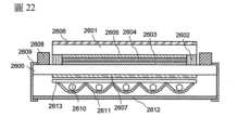
2600:TFT基板2600: TFT substrate
2601:對置基板2601: Opposing substrate
2602:密封材料2602: Sealing material
2603:像素部2603:Pixel Department
2604:顯示元件2604: Display component
2605:著色層2605: Coloring layer
2606:偏光板2606: Polarizing plate
2607:偏光板2607: Polarizing plate
2608:佈線電路部2608: Wiring circuit department
2609:撓性線路板2609: Flexible circuit board
2610:冷陰極管2610:Cold cathode tube
2611:反射板2611:Reflector
2612:電路基板2612: Circuit board
2613:擴散板2613:Diffusion plate
2631:海報2631:Poster
2632:車廂廣告2632:Train advertising
2700:電子書2700: e-books
2701:外殼2701: Shell
2703:外殼2703: Shell
2705:顯示部2705: Display unit
2707:顯示部2707: Display unit
2721:電源2721: Power supply
2723:操作鍵2723: Operation keys
2725:揚聲器2725: Speaker
4001:第一基板4001: First substrate
4002:像素部4002: Pixel Department
4003:信號線驅動電路4003:Signal line drive circuit
4004:掃描線驅動電路4004: Scan line drive circuit
4005:密封材料4005: Sealing material
4006:第二基板4006: Second substrate
4008:液晶層4008: Liquid crystal layer
4010:薄膜電晶體4010: Thin Film Transistor
4011:薄膜電晶體4011: Thin Film Transistor
4013:液晶元件4013: Liquid crystal element
4015:連接端子電極4015:Connecting terminal electrode
4016:端子電極4016: Terminal electrode
4020:絕緣層4020: Insulation layer
4021:絕緣層4021: Insulation layer
4030:像素電極層4030: Pixel electrode layer
4031:對置電極層4031: Opposing electrode layer
4032:絕緣層4032: Insulation layer
4033:絕緣層4033: Insulation layer
4501:第一基板4501: First substrate
4502:像素部4502: Pixel Department
4503a:信號線驅動電路4503a:Signal line driver circuit
4503b:信號線驅動電路4503b:Signal line driver circuit
4504a:掃描線驅動電路4504a: Scan line driver circuit
4504b:掃描線驅動電路4504b: Scan line drive circuit
4505:密封材料4505: Sealing material
4506:第二基板4506: Second substrate
4507:填料4507: Filler
4509:薄膜電晶體4509:Thin Film Transistor
4510:薄膜電晶體4510: Thin Film Transistor
4511:發光元件4511: Light-emitting element
4512:電場發光層4512:Electroluminescent layer
4513:第二電極層4513: Second electrode layer
4515:端子電極4515:Terminal electrode
4517:第一電極層4517:First electrode layer
4518a:FPC4518a:FPC
4518b:FPC4518b:FPC
4519:各向異性導電膜4519:Anisotropic conductive film
4520:分隔壁4520: Partition wall
6400:像素6400: pixels
6401:開關電晶體6401: Switching transistor
6402:驅動電晶體6402:Drive transistor
6403:電容元件6403: Capacitor components
6404:發光元件6404: Light-emitting element
6406:掃描線6406: Scan line
6405:信號線6405:Signal line
6407:電源線6407: Power cord
6408:共同電極6408: Common electrode
7001:驅動TFT7001: Driving TFT
7002:發光元件7002: Light-emitting element
7003:陰極7003: cathode
7004:發光層7004: Luminescent layer
7005:陽極7005: Yang pole
7011:驅動TFT7011: Driving TFT
7014:發光層7014: Luminescent layer
7015:陽極7015: Yang pole
7016:遮罩膜7016: Masking film
7021:TFT7021:TFT
7022:發光元件7022: Light-emitting element
7023:陰極7023: cathode
7024:發光層7024: Luminescent layer
7025:陽極7025: Yang pole
7027:導電膜7027: Conductive film
9201:顯示部9201: Display unit
9203:操作開關9203: Operation switch
9205:調節部9205: Adjustment Department
9206:相機部9206: Camera Department
9207:揚聲器9207: Speaker
9208:麥克風9208: Microphone
9301:頂外殼9301: Top shell
9302:底外殼9302: Bottom shell
9303:顯示部9303: Display unit
9304:鍵盤9304:Keyboard
9305:外部連接埠9305: External port
9306:定位裝置9306: Positioning device
9600:電視機9600:TV
9601:外殼9601: Shell
9603:顯示部9603: Display unit
9605:支架9605: Bracket
9607:顯示部9607: Display unit
9609:操作鍵9609: Operation key
9610:遙控器9610: Remote control
9700:數位相框9700: Digital photo frame
9701:外殼9701: Shell
9703:顯示部9703: Display unit
9881:外殼9881: Shell
9882:顯示部9882: Display unit
9883:顯示部9883: Display unit
9884:揚聲器部9884: Speaker unit
9885:操作鍵9885: Operation key
9886:記錄媒體插入部9886: Recording media insertion unit
9887:連接端子9887:Connection terminal
9888:感測器9888:Sensor
9890:LED燈9890:LED light
9891:外殼9891: Shell
9893:連接部9893:Connection part
9900:投幣機9900: Coin machine
9901:外殼9901: Shell
9903:顯示部9903: Display unit
在附圖中:In the attached picture:
圖1A和圖1B是說明半導體裝置的圖;Figures 1A and 1B are diagrams illustrating a semiconductor device;
圖2A至圖2E是說明半導體裝置的製造方法的圖;Figures 2A to 2E are diagrams illustrating a method for manufacturing a semiconductor device;
圖3A和圖3B是說明半導體裝置的圖;Figures 3A and 3B are diagrams illustrating semiconductor devices;
圖4A至圖4E是說明半導體裝置的製造方法的圖;Figures 4A to 4E are diagrams illustrating a method for manufacturing a semiconductor device;
圖5A和圖5B是說明半導體裝置的圖;Figures 5A and 5B are diagrams illustrating a semiconductor device;
圖6A至圖6E是說明半導體裝置的製造方法的圖;Figures 6A to 6E are diagrams illustrating a method for manufacturing a semiconductor device;
圖7A和圖7B是說明半導體裝置的圖;Figures 7A and 7B are diagrams illustrating a semiconductor device;
圖8A至圖8E是說明半導體裝置的製造方法的圖;Figures 8A to 8E are diagrams illustrating a method for manufacturing a semiconductor device;
圖9A至圖9C是說明半導體裝置的製造方法的圖;Figures 9A to 9C are diagrams illustrating a method for manufacturing a semiconductor device;
圖10A至圖10C是說明半導體裝置的製造方法的圖;Figures 10A to 10C are diagrams illustrating a method for manufacturing a semiconductor device;
圖11是說明半導體裝置的製造方法的圖;FIG11 is a diagram illustrating a method for manufacturing a semiconductor device;
圖12是說明半導體裝置的製造方法的圖;FIG12 is a diagram illustrating a method for manufacturing a semiconductor device;
圖13是說明半導體裝置的製造方法的圖;FIG13 is a diagram illustrating a method for manufacturing a semiconductor device;
圖14是說明半導體裝置的圖;FIG14 is a diagram illustrating a semiconductor device;
圖15A1、圖15A2、圖15B1及圖15B2是說明半導體裝置的圖;Figures 15A1, 15A2, 15B1 and 15B2 are diagrams for explaining semiconductor devices;
圖16是說明半導體裝置的圖;FIG16 is a diagram illustrating a semiconductor device;
圖17是說明半導體裝置的圖;FIG17 is a diagram illustrating a semiconductor device;
圖18A1、圖18A2及圖18B是說明半導體裝置的圖;Figures 18A1, 18A2 and 18B are diagrams for explaining semiconductor devices;
圖19A和圖19B是說明半導體裝置的圖;Figures 19A and 19B are diagrams illustrating a semiconductor device;
圖20是說明半導體裝置的像素等效電路的圖;FIG20 is a diagram illustrating a pixel equivalent circuit of a semiconductor device;
圖21A至圖21C是說明半導體裝置的圖;Figures 21A to 21C are diagrams illustrating semiconductor devices;
圖22是說明半導體裝置的圖;FIG22 is a diagram illustrating a semiconductor device;
圖23A和圖23B是說明電子紙的使用方式的例子的圖;Figures 23A and 23B are diagrams illustrating examples of how electronic paper is used;
圖24是顯示電子書籍的一例的外觀圖;Figure 24 is an appearance diagram showing an example of an electronic book;
圖25A和圖25B是顯示電視裝置及數位相框的例子的外觀圖;FIG. 25A and FIG. 25B are external views showing examples of a television device and a digital photo frame;
圖26A和圖26B是顯示遊戲機的例子的外觀圖;Figures 26A and 26B are external views showing an example of a game console;
圖27A和圖27B是顯示可攜式電腦及行動電話機的一例的外觀圖;Figures 27A and 27B are external views showing an example of a portable computer and a mobile phone;
圖28是顯示根據計算得到的結構的圖;Figure 28 is a diagram showing the structure obtained based on the calculation;
圖29是顯示根據計算得到的結構的圖;Figure 29 is a diagram showing the structure obtained based on the calculation;
圖30A至圖30C是顯示根據計算得到的態密度的圖;Figures 30A to 30C are graphs showing the state density obtained based on the calculation;
圖31A至圖31D是顯示根據計算得到的態密度的圖;Figures 31A to 31D are graphs showing the state density obtained based on the calculation;
圖32A至圖32D是顯示根據計算得到的態密度的圖;Figures 32A to 32D are graphs showing the state density obtained based on the calculation;
圖33A和圖33B是顯示根據計算得到的態密度的圖;Figures 33A and 33B are graphs showing the state density obtained based on the calculation;
圖34A和圖34B是顯示根據計算得到的結構的圖;Figures 34A and 34B are diagrams showing the structures obtained based on the calculation;
圖35是顯示計算前後的原子密度的圖。Figure 35 is a graph showing the atomic density before and after calculation.
使用附圖詳細地說明本發明的實施例。但是,本發明不侷限於以下的說明,本領域的技術人員能夠容易地理解,其方式和細節可以在不脫離本發明的宗旨及其範圍的條件下作各種各樣的變換。因此,所揭露的發明不應該被解釋為僅限於以下所示的實施例的記載內容。在以下說明的結構中,在不同附圖中使用相同的附圖標記來表示相同的部分或具有相同功能的部分,而省略重複說明。The embodiments of the present invention are described in detail using the accompanying drawings. However, the present invention is not limited to the following description, and a person skilled in the art can easily understand that the methods and details can be changed in various ways without departing from the purpose and scope of the present invention. Therefore, the disclosed invention should not be interpreted as being limited to the contents of the embodiments shown below. In the structures described below, the same figure marks are used in different figures to represent the same parts or parts with the same functions, and repeated descriptions are omitted.
(實施例1)(Implementation Example 1)
參照圖1A至圖2E說明半導體裝置及半導體裝置的製造方法。A semiconductor device and a method for manufacturing the semiconductor device are described with reference to FIGS. 1A to 2E.
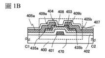
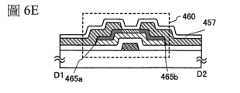
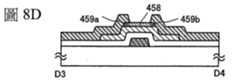
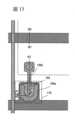
圖1A是半導體裝置所具有的薄膜電晶體470的平面圖,而圖1B是沿著圖1A的線C1-C2的截面圖。薄膜電晶體470是反堆疊型薄膜電晶體,並在具有絕緣表面的基板400上包括閘極電極層401、閘極絕緣層402、半導體層403、緩衝層404及源極電極層及汲極電極層405a、405b。另外,設置有覆蓋薄膜電晶體470且與緩衝層404的絕緣膜407接觸。FIG1A is a plan view of a
緩衝層404包括:與源極電極層及汲極電極層405a、405b的低電阻區域接觸的第一區域409a、409b;以及與半導體層403的通道形成區的高電阻區域接觸的第二區域408。注意,在說明書的附圖中,將緩衝層404、半導體層403的陰影部分的區域表示為低電阻區域的第一區域409a、409b、低電阻區域435a、435b。The
緩衝層404在其膜中具有電阻分佈。設置在半導體層403的通道形成區上的第二區域408的導電率低於半導體層403的通道形成區的導電率,並且接觸於源極電極層及汲極電極層405a、405b的第一區域409a、409b的導電率高於半導體層403的通道形成區的導電率。另外,與閘極絕緣層402相比,緩衝層404及半導體層403的導電率高(電阻低)。因此,按照導電率從高到低的排列順序,其分別為緩衝層404的低電阻區域(第一區域409a、409b)、半導體層403的通道形成區、緩衝層404的高電阻區域(第二區域408)、閘極絕緣層402。The
因為緩衝層中的接觸於通道形成區的區域為高電阻區域,所以薄膜電晶體的電特性穩定化,而可以防止截止電流的增加等。另一方面,因為緩衝層中的接觸於源極電極層及汲極電極層的區域為低電阻區域,所以接觸電阻低,而可以使導通電流增高。因此,可以製造包括電特性高且可靠性高的薄膜電晶體的半導體裝置。Since the area in the buffer layer that contacts the channel formation area is a high resistance area, the electrical characteristics of the thin film transistor are stabilized, and the increase of the cut-off current can be prevented. On the other hand, since the area in the buffer layer that contacts the source electrode layer and the drain electrode layer is a low resistance area, the contact resistance is low, and the conduction current can be increased. Therefore, a semiconductor device including a thin film transistor with high electrical characteristics and high reliability can be manufactured.
作為緩衝層404,可以使用包含鈦、鉬或錳的氧化物半導體層。藉由使氧化物半導體層包含鈦、鉬或錳的金屬元素,氧化物半導體層的電阻增大。As the
對具有如下結構的電子狀態進行計算,在該結構中作為緩衝層404的例子使In-Ga-Zn-O類氧化物半導體包含鈦(Ti)或鉬(Mo)。以下示出計算方法。The electronic state of a structure in which an In-Ga-Zn-O-based oxide semiconductor contains titanium (Ti) or molybdenum (Mo) as an example of a
將包含Ti的In-Ga-Zn-O類氧化物半導體結構的密度和包含Mo的In-Ga-Zn-O類氧化物半導體結構的密度固定於非晶In-Ga-Zn-O類氧化物半導體的實驗值的5.9g/cm3。以下述計算條件對上述兩個結構進行計算。另外,作為經典分子動力學(MD)計算,使用富士通株式會社製造的計算軟體Materials Explorer 5.0。作為第一原理計算,使用Accelrys K.K.製造的第一原子計算軟體CASTEP。The density of the In-Ga-Zn-O-based oxide semiconductor structure containing Ti and the density of the In-Ga-Zn-O-based oxide semiconductor structure containing Mo were fixed to 5.9 g/cm3 , which is the experimental value of amorphous In-Ga-Zn-O-based oxide semiconductors. The above two structures were calculated under the following calculation conditions. In addition, as a classical molecular dynamics (MD) calculation, the calculation software Materials Explorer 5.0 manufactured by Fujitsu Limited was used. As a first principle calculation, the first atomic calculation software CASTEP manufactured by Accelrys KK was used.
首先,使藉由經典分子動力學(MD)計算和第一原理計算製造的In-Ga-Zn-O類氧化物半導體包含Ti或Mo。接著,在第一原理MD計算中,將溫度從3000K降低至1500K、300K,並且以如下條件進行計算,該條件是:粒子數(N)、體積(V)、溫度(T)是一定(系綜NVT);時間步長是1fsec;各溫度下的步數是2000step;電子的截止能量(cut-off energy)是260eV;倒晶格(reciprocal lattice)的網格(k點)為1×1×1,最後藉由以如下條件進行第一原理計算而進行結構的最適化,該條件是:電子的截止能量是420eV;倒晶格的網格(k點)為2×2×2。First, the In-Ga-Zn-O oxide semiconductor manufactured by classical molecular dynamics (MD) calculation and first principle calculation contains Ti or Mo. Then, in the first principle MD calculation, the temperature is lowered from 3000K to 1500K and 300K, and the calculation is performed under the following conditions: the number of particles (N), volume (V), and temperature (T) are constant (system NVT); the time step is 1fsec; the number of steps at each temperature is 2000step; the cut-off energy of the electron is 260eV; the grid (k point) of the reciprocal lattice is 1×1×1, and finally the structure is optimized by performing the first principle calculation under the following conditions: the cut-off energy of the electron is 420eV; the grid (k point) of the reciprocal lattice is 2×2×2.
圖28及圖29示出藉由計算得到的包含Ti或Mo的In-Ga-Zn-O類氧化物半導體結構的結構。黑色圓點表示金屬原子,而白色圓點表示氧原子。大的黑色圓點是Ti或Mo。在圖28的包含Ti的In-Ga-Zn-O類氧化物半導體結構中,In、Ga、Zn的原子數分別是12個,O的原子數是50個,並且Ti的原子數是1個。在圖29的包含Mo的In-Ga-Zn-O類氧化物半導體結構中,In、Ga、Zn的原子數分別是12個,O的原子數是51個,並且Mo的原子數是1個。Figures 28 and 29 show the structure of an In-Ga-Zn-O type oxide semiconductor structure containing Ti or Mo obtained by calculation. Black dots represent metal atoms, and white dots represent oxygen atoms. The large black dots are Ti or Mo. In the In-Ga-Zn-O type oxide semiconductor structure containing Ti in Figure 28, the number of In, Ga, and Zn atoms is 12, the number of O atoms is 50, and the number of Ti atoms is 1. In the In-Ga-Zn-O type oxide semiconductor structure containing Mo in Figure 29, the number of In, Ga, and Zn atoms is 12, the number of O atoms is 51, and the number of Mo atoms is 1.
藉由第一原理計算並以以下條件對圖28及圖29的包含Ti的In-Ga-Zn-O類氧化物半導體結構及包含Mo的In-Ga-Zn-O類氧化物半導體結構進行計算,以求出電子的態密度,該條件是:電子的截止能量是420eV;倒晶格的網格(k點)為3×3×3。The electron state density is calculated by first principle calculations for the In-Ga-Zn-O type oxide semiconductor structure containing Ti and the In-Ga-Zn-O type oxide semiconductor structure containing Mo in Figures 28 and 29 under the following conditions: the cutoff energy of the electron is 420eV; the grid (k point) of the reciprocal lattice is 3×3×3.
圖30A示出In-Ga-Zn-O類氧化物半導體結構整體的態密度,圖30B示出包含Ti的In-Ga-Zn-O類氧化物半導體結構整體的態密度,並且圖30C示出包含Mo的In-Ga-Zn-O類氧化物半導體結構整體的態密度。在圖30A、圖30B、圖30C中,將費米能(Fermi energy)設定為橫軸的原點。在圖30A的In-Ga-Zn-O類氧化物半導體結構中、在圖30B的包含Ti的In-Ga-Zn-O類氧化物半導體結構中、在圖30C的包含Mo的In-Ga-Zn-O類氧化物半導體結構中都有帶隙,並且價帶上端、傳導帶下端位於圖中所示的位置。費米能在價帶上端。FIG. 30A shows the state density of the entire In-Ga-Zn-O type oxide semiconductor structure, FIG. 30B shows the state density of the entire In-Ga-Zn-O type oxide semiconductor structure containing Ti, and FIG. 30C shows the state density of the entire In-Ga-Zn-O type oxide semiconductor structure containing Mo. In FIG. 30A, FIG. 30B, and FIG. 30C, the Fermi energy is set as the origin of the horizontal axis. In the In-Ga-Zn-O type oxide semiconductor structure of FIG. 30A, in the In-Ga-Zn-O type oxide semiconductor structure containing Ti of FIG. 30B, and in the In-Ga-Zn-O type oxide semiconductor structure containing Mo of FIG. 30C, there are band gaps, and the upper end of the valence band and the lower end of the conduction band are located at the positions shown in the figure. The Fermi energy is at the upper end of the valence band.
圖31A示出包含Ti的In-Ga-Zn-O類氧化物半導體結構的每個In原子的部分態密度,圖31B示出包含Ti的In-Ga-Zn-O類氧化物半導體結構的每個Ga原子的部分態密度,圖31C示出包含Ti的In-Ga-Zn-O類氧化物半導體結構的每個Zn原子的部分態密度。圖32A示出包含Mo的In-Ga-Zn-O類氧化物半導體結構的每個In原子的部分態密度,圖32B示出包含Mo的In-Ga-Zn-O類氧化物半導體結構的每個Ga原子的部分態密度,圖32C示出包含Mo的In-Ga-Zn-O類氧化物半導體結構的每個Zn原子的部分態密度。上述原子在系內分別有12個,在此採用其平均值。根據圖31A至圖31C及圖32A至圖32C的結果,可知n型載子進入的傳導帶下端近旁的能級主要由In、Ga、Zn的s軌道形成。FIG. 31A shows the partial state density of each In atom of an In-Ga-Zn-O type oxide semiconductor structure containing Ti, FIG. 31B shows the partial state density of each Ga atom of an In-Ga-Zn-O type oxide semiconductor structure containing Ti, and FIG. 31C shows the partial state density of each Zn atom of an In-Ga-Zn-O type oxide semiconductor structure containing Ti. FIG. 32A shows the partial state density of each In atom of an In-Ga-Zn-O type oxide semiconductor structure containing Mo, FIG. 32B shows the partial state density of each Ga atom of an In-Ga-Zn-O type oxide semiconductor structure containing Mo, and FIG. 32C shows the partial state density of each Zn atom of an In-Ga-Zn-O type oxide semiconductor structure containing Mo. There are 12 atoms in the system, and their average values are used here. According to the results of Figures 31A to 31C and Figures 32A to 32C, it can be seen that the energy level near the lower end of the conduction band where n-type carriers enter is mainly formed by the s-orbit of In, Ga, and Zn.
圖31D示出包含Ti的In-Ga-Zn-O類氧化物半導體結構的Ti的部分態密度,而圖32D示出包含Mo的In-Ga-Zn-O類氧化物半導體結構的Mo的部分態密度。根據圖31D及圖32D的結果,可知最有影響的不是s軌道,而是d軌道。當使Ti、Mo的濃度變高時,傳導帶下端的能級不由In、Ga、Zn的s軌道構成而由Ti、Mo的d軌道構成。d軌道的各向異性高於s軌道的各向異性,並且d軌道在非晶結構中不容易傳導n型載子,因此遷移率降低。FIG31D shows the partial state density of Ti in an In-Ga-Zn-O type oxide semiconductor structure containing Ti, and FIG32D shows the partial state density of Mo in an In-Ga-Zn-O type oxide semiconductor structure containing Mo. According to the results of FIG31D and FIG32D, it can be seen that the most influential is not the s-orbit but the d-orbit. When the concentration of Ti and Mo is increased, the energy level at the lower end of the conduction band is not composed of the s-orbit of In, Ga, and Zn but of the d-orbit of Ti and Mo. The anisotropy of the d-orbit is higher than that of the s-orbit, and the d-orbit is not easy to conduct n-type carriers in an amorphous structure, so the mobility is reduced.
據此,可知當使Ti、Mo包含在In-Ga-Zn-O類氧化物半導體中時,其成為隨著高濃度增大,難以流過n型載子的導電率低的膜。因此,藉由使其d軌道、f軌道空著的過渡金屬元素的Ti、Mo包含在氧化物半導體層中,可以降低導電率(實現高電阻化)。Based on this, it can be seen that when Ti and Mo are included in In-Ga-Zn-O-based oxide semiconductors, it becomes a film with low conductivity that makes it difficult for n-type carriers to flow as the concentration increases. Therefore, by including Ti and Mo, transition metal elements whose d-orbit and f-orbit are vacant, in the oxide semiconductor layer, the conductivity can be reduced (high resistance can be achieved).
注意,作為源極電極層及汲極電極層405a、405b,較佳使用含有對氧的親和性高的金屬的材料。另外,上述對氧的親和性高的金屬較佳為選自鈦、鋁、錳、鎂、鋯、鈹、釷中的一者或多種的材料。Note that as the source electrode layer and the
與緩衝層404接觸的源極電極層及汲極電極層405a、405b較佳使用對氧的親和性高的金屬。作為對氧的親和性高的金屬,例如可以舉出鈦、鋁、錳、鎂、鋯、鈹、釷等的與鋅相比其標準電極電位小的金屬。另外,也可以使用銅等。如上所述,藉由採用對氧的親和性高的金屬與氧化物半導體層接觸的結構並進行熱處理等,作為氧化物半導體層的緩衝層404的接觸於源極電極層及汲極電極層405a、405b的區域的氧的組成比小於其他區域的氧的組成比。因為在該低氧區域中有導電性提高的趨勢,所以成為低電阻區域。另外,對氧的親和性高的金屬不侷限於上述材料。The source electrode layer and the
由於上述現象起因於對氧的親和性高的金屬使氧從氧化物半導體層脫嵌,所以可以得知在電極層中與氧化物半導體層接觸的區域中的氧的組成比大於其他區域的氧的組成比(換言之,在該區域中電極層被氧化)。考慮到上述情況,形成在電極層中的接觸於氧化物半導體層的區域中的金屬氧化物較佳具有導電性。例如,當作為對氧的親和性高的金屬使用鈦時,以形成近於一氧化物的組成比(例如,當採用TiOx時大致是0.5<x<1.5)的氧化物的條件進行各種處理即可。這是因為鈦的一氧化物具有導電性而鈦的二氧化物具有絕緣性的緣故。Since the above phenomenon is caused by the metal with high affinity for oxygen causing oxygen to be de-embedded from the oxide semiconductor layer, it can be known that the composition ratio of oxygen in the region in contact with the oxide semiconductor layer in the electrode layer is greater than the composition ratio of oxygen in other regions (in other words, the electrode layer is oxidized in this region). Considering the above situation, the metal oxide formed in the region in contact with the oxide semiconductor layer in the electrode layer is preferably conductive. For example, when titanium is used as the metal with high affinity for oxygen, various treatments can be performed under conditions to form an oxide with a composition ratio close to that of monoxide (for example, when TiOx is used, it is approximately 0.5<x<1.5). This is because titanium monoxide has conductivity and titanium dioxide has insulation.
在此,基於計算模擬說明將對氧的親和性高的金屬用作電極層的情況的效果。雖然在此對將鈦用作對氧的親和性高的金屬並將In-Ga-Zn-O類氧化物半導體材料用作氧化物半導體層的情況進行計算,但是所揭露的發明的一個方式不侷限於此。另外,在計算中,將In-Ga-Zn-O類氧化物半導體材料的組成設定為In:Ga:Zn:O=1:1:1:4。Here, the effect of using a metal with a high affinity for oxygen as an electrode layer is described based on calculation simulation. Although the calculation is performed here for the case where titanium is used as a metal with a high affinity for oxygen and an In-Ga-Zn-O type oxide semiconductor material is used as an oxide semiconductor layer, the disclosed invention is not limited to this. In addition, in the calculation, the composition of the In-Ga-Zn-O type oxide semiconductor material is set to In:Ga:Zn:O=1:1:1:4.
首先,驗證氧從非晶狀態的氧化物半導體消失所產生的效果。First, verify the effect of oxygen disappearing from amorphous oxide semiconductors.
藉由使用經典MD(分子動力學)計算的熔融淬火法(melt-quench法),準備In-Ga-Zn-O類氧化物半導體的非晶結構。在此,對其總原子數是84個,密度是5.9g/cm3的結構進行計算。至於金屬-氧間及氧-氧間的內在位能使用Born-Mayer-Huggins位能,而至於金屬-金屬間的內在位能使用Lennard-Jones位能,並以NVT系綜進行計算。作為計算程式,使用Matereials Explorer。The amorphous structure of In-Ga-Zn-O oxide semiconductor was prepared by melt-quenching method using classical MD (molecular dynamics) calculation. Here, the total number of atoms is 84 and the density is 5.9g/cm3 . The intrinsic potential between metal and oxygen and between oxygen and oxygen is calculated by Born-Mayer-Huggins potential, and the intrinsic potential between metal and metal is calculated by Lennard-Jones potential, and the NVT system is used. Matereials Explorer is used as the calculation program.
然後,藉由使用基於密度泛函理論(Density Functional Theory:DFT)的平面波贗勢方法的第一原理計算(量子MD計算),對藉由上述經典MD計算得出的結構進行最適化,以求出態密度。另外,對去除任意一個氧原子的結構也進行最適化,以計算態密度。作為計算程式使用CASTEP,並且作為交換相關泛函使用GGA-PBE。Then, the structure obtained by the above classical MD calculation was optimized by first principle calculation (quantum MD calculation) using the plane wave potential method based on density functional theory (DFT) to obtain the state density. In addition, the structure with any oxygen atom removed was also optimized to calculate the state density. CASTEP was used as the calculation program, and GGA-PBE was used as the exchange correlation functional.
圖33A和圖33B示出藉由上述計算結果得出的結構的態密度。圖33A是沒有氧缺損的結構的態密度,而圖33B是有氧缺損的結構的態密度。在此,0(eV)表示對應於費米能階的能量。根據圖33A及圖33B,可知在沒有氧缺損的結構中費米能階存在於價帶的上端,與此相對,在有氧缺損的結構中費米能階存在於傳導帶中。因為在有氧缺損的結構中費米能階存在於傳導帶中,所以影響到傳導的電子數增加,以得到低電阻(高導電率)的結構。FIG33A and FIG33B show the state density of the structure obtained by the above calculation results. FIG33A is the state density of the structure without oxygen deficiency, and FIG33B is the state density of the structure with oxygen deficiency. Here, 0 (eV) represents the energy corresponding to the Fermi level. According to FIG33A and FIG33B, it can be seen that in the structure without oxygen deficiency, the Fermi level exists at the upper end of the valence band, while in the structure with oxygen deficiency, the Fermi level exists in the conduction band. Since the Fermi level exists in the conduction band in the structure with oxygen deficiency, the number of electrons that are conducted increases, thereby obtaining a low resistance (high conductivity) structure.
接著,藉由作為電極層使用對氧的親和性高的金屬,確認到氧從非晶狀態的氧化物半導體移動到對氧的親和性高的金屬的樣子。Next, by using a metal with a high affinity for oxygen as the electrode layer, it was confirmed that oxygen was moving from the amorphous oxide semiconductor to the metal with a high affinity for oxygen.
在此,在藉由上述第一原理計算得出的In-Ga-Zn-O類非晶結構上層疊鈦晶體,並且以NVT系綜對該結構進行量子MD計算。作為計算程式使用CASTEP,並且作為交換相關泛函使用GGA-PBE。另外,將溫度條件設定為623K(350℃)。Here, a titanium crystal is stacked on the In-Ga-Zn-O amorphous structure obtained by the first principle calculation, and the structure is subjected to quantum MD calculation using the NVT system. CASTEP is used as the calculation program, and GGA-PBE is used as the exchange correlation functional. In addition, the temperature condition is set to 623K (350℃).
圖34A和圖34B示出實施量子MD計算前後的結構。圖34A是實施量子MD計算之前的結構,而圖34B是實施量子MD計算之後的結構。在實施量子MD計算之後的結構中,與實施量子MD計算之前相比與鈦接合的氧的數量增加。該結構變化示出氧原子從非晶狀態的氧化物半導體層移動到對氧的親和性高的金屬層。Figures 34A and 34B show the structures before and after the quantum MD calculation is performed. Figure 34A is the structure before the quantum MD calculation is performed, and Figure 34B is the structure after the quantum MD calculation is performed. In the structure after the quantum MD calculation is performed, the amount of oxygen bonded to titanium increases compared to before the quantum MD calculation is performed. This structural change shows that oxygen atoms move from the oxide semiconductor layer in an amorphous state to the metal layer with a high affinity for oxygen.
圖35示出實施量子MD計算的前後的鈦及氧的密度。各曲線分別表示實施量子MD計算之前的鈦密度(Ti_before)、實施量子MD計算之後的鈦密度(Ti_after)、實施量子MD計算之前的氧密度(O_before)、實施量子MD計算之後的氧密度(O_after)。根據圖35也可知氧原子移動到對氧的親和性高的金屬。Figure 35 shows the density of titanium and oxygen before and after the quantum MD calculation. The curves represent the titanium density before the quantum MD calculation (Ti_before), the titanium density after the quantum MD calculation (Ti_after), the oxygen density before the quantum MD calculation (O_before), and the oxygen density after the quantum MD calculation (O_after). Figure 35 also shows that oxygen atoms move to metals with high affinity for oxygen.
據此,確認:藉由使氧化物半導體層與對氧的親和性高的金屬層接觸地進行熱處理,氧原子從氧化物半導體層移動到金屬層,以使介面附近的載子密度增高。該現象示出在介面附近形成低電阻區域,而可以說該現象發揮降低半導體層與電極層的接觸電阻的效果。Based on this, it was confirmed that by heat-treating an oxide semiconductor layer in contact with a metal layer with high affinity for oxygen, oxygen atoms moved from the oxide semiconductor layer to the metal layer, thereby increasing the carrier density near the interface. This phenomenon shows that a low-resistance region is formed near the interface, and it can be said that this phenomenon has the effect of reducing the contact resistance between the semiconductor layer and the electrode layer.
作為包括通道形成區的半導體層403,使用具有半導體特性的氧化物材料即可。例如,可以使用具有表示為InMO3(ZnO)m(m>0)的結構的氧化物半導體,特別最好使用In-Ga-Zn-O類氧化物半導體。另外,M表示選自鎵(Ga)、鐵(Fe)、鎳(Ni)、錳(Mn)和鈷(Co)中的一者金屬元素或多種金屬元素。例如,作為M,除了有包含Ga的情況之外,還有包含Ga和Ni或Ga和Fe等的Ga以外的上述金屬元素的情況。此外,在上述氧化物半導體中,有除了包含作為M的金屬元素的情況之外,還有包含諸如Fe或Ni等的其他過渡金屬元素或者該過渡金屬的氧化物作為雜質元素的情況。在本說明書中,將在具有表示為InMO3(ZnO)m(m>0)的結構的氧化物半導體中的具有作為M至少包含Ga的結構的氧化物半導體稱為In-Ga-Zn-O類氧化物半導體,並且將該薄膜也稱為In-Ga-Zn-O類非單晶膜。As the
另外,作為用於氧化物半導體層的氧化物半導體,除了可以使用上述材料之外,還可以使用In-Sn-Zn-O類、In-Al-Zn-O類、Sn-Ga-Zn-O類、Al-Ga-Zn-O類、Sn-Al-Zn-O類、In-Zn-O類、Sn-Zn-O類、Al-Zn-O類、In-O類、Sn-O類、Zn-O類的氧化物半導體。In addition, as oxide semiconductors used for the oxide semiconductor layer, in addition to the above materials, In-Sn-Zn-O, In-Al-Zn-O, Sn-Ga-Zn-O, Al-Ga-Zn-O, Sn-Al-Zn-O, In-Zn-O, Sn-Zn-O, Al-Zn-O, In-O, Sn-O, and Zn-O oxide semiconductors can also be used.
圖2A至2E相當於示出薄膜電晶體470的製造步驟的截面圖。Figures 2A to 2E are equivalent to cross-sectional views showing the manufacturing steps of the
在圖2A中,在具有絕緣表面的基板400上設置閘極電極層401。也可以在基板400和閘極電極層401之間設置成為基底膜的絕緣膜。基底膜具有防止來自基板400的雜質元素的擴散的功能,並且其可以使用選自氮化矽膜、氧化矽膜、氮氧化矽膜或氧氮化矽膜中的一者或多種膜的疊層結構形成。閘極電極層401的材料可以藉由使用鉬、鈦、鉻、鉭、鎢、鋁、銅、釹或鈧等的金屬材料或以這些材料為主要成分的合金材料的單層或疊層來形成。In FIG. 2A , a
例如,作為閘極電極層401的雙層的疊層結構,最好採用:在鋁層上層疊有鉬層的雙層結構;在銅層上層疊有鉬層的雙層結構;在銅層上層疊有氮化鈦層或氮化鉭層的雙層結構;或者層疊有氮化鈦層和鉬層的雙層結構。作為三層的疊層結構,最好採用層疊如下層的結構:鎢層或氮化鎢層;鋁和矽的合金層或鋁和鈦的合金層;以及氮化鈦層或鈦層。For example, as the double-layer stacked structure of the
在閘極電極層401上形成閘極絕緣層402。A
藉由利用電漿CVD法或濺射法等並使用氧化矽層、氮化矽層、氧氮化矽層或氮氧化矽層的單層或疊層,可以形成閘極絕緣層402。另外,作為閘極絕緣層402,還可以藉由使用有機矽烷氣體的CVD法而形成氧化矽層。作為有機矽烷氣體,可以使用正矽酸乙酯(TEOS:化學式為Si(OC2H5)4)、四甲基矽烷(TMS:化學式為Si(CH3)4)、四甲基環四矽氧烷(TMCTS)、八甲基環四矽氧烷(OMCTS)、六甲基二矽氮烷(HMDS)、三乙氧基矽烷(化學式為SiH(OC2H5)3)、三(二甲氨基)矽烷(化學式為SiH(N(CH3)2)3)等含有矽的化合物。The
在閘極絕緣層402上依次層疊第一氧化物半導體膜433、第二氧化物半導體膜434(參照圖2A)。A first
注意,較佳在藉由濺射法形成第一氧化物半導體膜433之前,進行藉由導入氬氣體來產生電漿的反濺射,而去除附著於閘極絕緣層402的表面的塵屑。反濺射是指一種方法,其中不對靶一側施加電壓而在氬氣圍下使用RF電源對基板一側施加電壓來在基板上產生電漿,以對表面進行改性。Note that it is preferable to perform back sputtering by introducing argon gas to generate plasma before forming the first
注意,也可以使用氮、氦等代替氬氣圍。另外,也可以在對氬氣圍加入氧、N2O等的氣圍下進行反濺射。另外,也可以在對氬氣圍中加入Cl2、CF4等的氣圍下進行反濺射。Note that nitrogen, helium, etc. may be used instead of the argon atmosphere. Also, back sputtering may be performed in an atmosphere in which oxygen, N2 O, etc. are added to the argon atmosphere. Also, back sputtering may be performed in an atmosphere in which Cl2 , CF4 , etc. are added to the argon atmosphere.
作為第一氧化物半導體膜433,使用In-Ga-Zn-O類非單晶膜。第一氧化物半導體膜433使用In-Ga-Zn-O類氧化物半導體靶並藉由濺射法形成。As the first
作為第二氧化物半導體膜434,使用包含鈦的In-Ga-Zn-O類非單晶膜。第二氧化物半導體膜434使用包含氧化鈦的In-Ga-Zn-O類氧化物半導體靶並藉由濺射法形成。As the second
也可以不接觸於大氣地連續形成閘極絕緣層402、第一氧化物半導體膜433、第二氧化物半導體膜434。藉由不接觸於大氣地連續形成閘極絕緣層402、第一氧化物半導體膜433、第二氧化物半導體膜434,可以不被大氣成分或懸浮在大氣中的雜質元素污染地形成各疊層介面,因此可以降低薄膜電晶體特性的不均勻性。The
藉由光刻步驟將第一氧化物半導體膜433、第二氧化物半導體膜434加工為作為島狀的氧化物半導體層的半導體層403、氧化物半導體層431。The first
在閘極絕緣層402、半導體層403及氧化物半導體層431上形成導電膜432(參照圖2B)。A
作為導電膜432的材料,使用作為對氧的親和性高的金屬的鈦膜。另外,也可以在鈦膜上層疊:選自Al、Cr、Ta、Mo、W中的元素;以上述元素為成分的合金;或組合了上述元素的合金膜等。As the material of the
藉由蝕刻步驟對氧化物半導體層431、導電膜432進行蝕刻,形成緩衝層404、源極電極層及汲極電極層405a、405b(參照圖2C)。另外,緩衝層404僅有一部分被蝕刻,而成為具有槽部(凹部)的緩衝層404。The
接著,對作為氧化物半導體層的緩衝層404及源極電極層及汲極電極層405a、405b進行加熱處理。藉由加熱處理,氧原子從氧化物半導體層移動到金屬層,因此,接觸於源極電極層及汲極電極層405a、405b的第一區域409a、409b的電阻降低。另一方面,接觸於半導體層403的通道形成區的第二區域408的電阻依然高。如上所述,在緩衝層404中形成作為低電阻區域的第一區域409a、409b以及作為高電阻區域的第二區域408(參照圖2D)。另外,藉由該加熱處理,在半導體層403的接觸於源極電極層及汲極電極層405a、405b的區域中也是,同樣地,氧原子從氧化物半導體層移動到金屬層,從而形成低電阻區域435a、435b。Next, the
加熱處理較佳以200℃至600℃,典型為以300℃至500℃進行。例如,在氮氣圍下進行350℃且一小時的熱處理。The heat treatment is preferably performed at 200°C to 600°C, typically at 300°C to 500°C. For example, heat treatment is performed at 350°C for one hour in a nitrogen atmosphere.
以上述步驟可以製造圖2E所示的反堆疊型的薄膜電晶體470。另外,覆蓋薄膜電晶體470且接觸於緩衝層404地形成絕緣膜407。The reverse stacked
因為緩衝層中的與通道形成區接觸的區域是高電阻區域,所以薄膜電晶體的電特性穩定化,以可以防止截止電流的增加等。另一方面,因為緩衝層的接觸於源極電極層及汲極電極層的區域是低電阻區域,所以其接觸電阻低,而可以使導通電流增高。因此,可以製造包括電特性高且可靠性高的薄膜電晶體的半導體裝置。Because the area in the buffer layer that contacts the channel formation area is a high resistance area, the electrical characteristics of the thin film transistor are stabilized to prevent the increase of the cut-off current. On the other hand, because the area in the buffer layer that contacts the source electrode layer and the drain electrode layer is a low resistance area, its contact resistance is low, and the on-current can be increased. Therefore, a semiconductor device including a thin film transistor with high electrical characteristics and high reliability can be manufactured.
在此,圖3A至圖4D示出包括如下薄膜電晶體的半導體裝置的例子,該薄膜電晶體在實施例1中以不同蝕刻步驟加工具有通道形成區的氧化物半導體層與緩衝層。從而,除了氧化物半導體層與緩衝層的形成以外,該薄膜電晶體可以與實施例1同樣地形成,而省略具有與實施例1相同的部分、相同的功能的部分以及步驟的重複的說明。Here, FIG. 3A to FIG. 4D show an example of a semiconductor device including a thin film transistor in which an oxide semiconductor layer and a buffer layer having a channel formation region are processed in different etching steps in
圖3A是半導體裝置所具有的薄膜電晶體471的平面圖,而圖3B是沿著圖3A的線C3-C4的截面圖。薄膜電晶體471是反堆疊型的薄膜電晶體,並在具有絕緣表面的基板400上包括閘極電極層401、閘極絕緣層402、半導體層403、緩衝層404、源極電極層及汲極電極層405a、405b。另外,覆蓋薄膜電晶體471且與緩衝層404接觸地設置有絕緣膜407。FIG3A is a plan view of a
緩衝層404包括與源極電極層及汲極電極層405a及405b接觸的作為低電阻區域的第一區域409a及409b以及與半導體層403的通道形成區接觸的作為高電阻區域的第二區域408。The
在薄膜電晶體471中,緩衝層404覆蓋半導體層403的端部且延伸到源極電極層及汲極電極層405a、405b下地形成。緩衝層404具有不與半導體層403重疊且接觸源極電極層405a或汲極電極層405b的區域。In the
圖4A至圖4E相當於示出薄膜電晶體471的製造步驟的截面圖。Figures 4A to 4E are equivalent to cross-sectional views showing the manufacturing steps of the
在具有絕緣表面的基板400上設置閘極電極層401,並且在閘極電極層401上形成閘極絕緣層402。A
在閘極絕緣層402上形成氧化物半導體膜並將其加工為島狀,而形成半導體層403(參照圖4A)。An oxide semiconductor film is formed on the
覆蓋加工為島狀的半導體層403上地形成氧化物半導體膜436,並且在氧化物半導體膜436上層疊導電膜432(參照圖4B)。氧化物半導體膜436是與實施例1中的第二氧化物半導體膜434相同的膜,使用包含鈦的In-Ga-Zn-O類非單晶膜。氧化物半導體膜436使用包含氧化鈦的In-Ga-Zn-O靶並藉由濺射法形成。An
作為導電膜432的材料,使用作為對氧的親和性高的金屬的鈦膜。As the material of the
藉由蝕刻步驟對氧化物半導體膜436、導電膜432進行蝕刻,而形成緩衝層404、源極電極層及汲極電極層405a、405b(參照圖4C)。另外,緩衝層404僅有一部分被蝕刻,而成為具有槽部(凹部)的緩衝層404。The
接著,對作為氧化物半導體層的緩衝層404及源極電極層及汲極電極層405a、405b進行加熱處理。藉由加熱處理,氧原子從氧化物半導體層移動到金屬層,因此,接觸於源極電極層及汲極電極層405a、405b的第一區域409a、409b的電阻降低。另一方面,接觸於半導體層403的通道形成區的第二區域408的電阻依然高。如上所述,在緩衝層404中形成作為低電阻區域的第一區域409a、409b以及作為高電阻區域的第二區域408(參照圖4D)。Next, the
加熱處理較佳以200℃至600℃,典型為以300℃至500℃進行。例如,在氮氣圍下進行350℃且一小時的熱處理。The heat treatment is preferably performed at 200°C to 600°C, typically at 300°C to 500°C. For example, heat treatment is performed at 350°C for one hour in a nitrogen atmosphere.
以上述步驟可以製造圖4E所示的反堆疊型的薄膜電晶體471。另外,覆蓋薄膜電晶體471且接觸於緩衝層404地形成絕緣膜407。The reverse stacked
如上所述,藉由在薄膜電晶體的製造步驟中使蝕刻加工的步驟順序變化,可以製造各種形狀不同的薄膜電晶體。As described above, by changing the order of etching steps in the manufacturing process of thin film transistors, thin film transistors of various shapes can be manufactured.
因為緩衝層中的接觸於通道形成區的區域為高電阻區域,所以薄膜電晶體的電特性穩定化,而可以防止截止電流的增加等。另一方面,因為緩衝層中的接觸於源極電極層及汲極電極層的區域為低電阻區域,所以接觸電阻低,而可以使導通電流增高。因此,可以製造包括電特性高且可靠性高的薄膜電晶體的半導體裝置。Since the area in the buffer layer that contacts the channel formation area is a high resistance area, the electrical characteristics of the thin film transistor are stabilized, and the increase of the cut-off current can be prevented. On the other hand, since the area in the buffer layer that contacts the source electrode layer and the drain electrode layer is a low resistance area, the contact resistance is low, and the conduction current can be increased. Therefore, a semiconductor device including a thin film transistor with high electrical characteristics and high reliability can be manufactured.
(實施例3)(Implementation Example 3)
使用圖5A至圖6E說明半導體裝置及半導體裝置的製造方法的別的例子。本實施例是在實施例1及實施例2中使用不同的緩衝層的材料及製造方法的例子。從而,除了緩衝層之外,本實施例的薄膜電晶體可以與實施例1及實施例2同樣地形成,而省略具有與實施例1及實施例2相同的部分、相同的功能的部分以及步驟的重複的說明。FIG. 5A to FIG. 6E are used to illustrate other examples of semiconductor devices and methods for manufacturing semiconductor devices. This embodiment is an example of using different buffer layer materials and manufacturing methods in
圖5A是半導體裝置所具有的薄膜電晶體460的平面圖,而圖5B是沿著圖5A的線D1-D2的截面圖。薄膜電晶體460是反堆疊型的薄膜電晶體,並在具有絕緣表面的基板450上包括閘極電極層451、閘極絕緣層452、半導體層453、緩衝層454、源極電極層及汲極電極層455a、455b。另外,覆蓋薄膜電晶體460且接觸於緩衝層454地設置有絕緣膜457。FIG5A is a plan view of a
緩衝層454包括接觸於源極電極層及汲極電極層455a、455b的作為低電阻區域的第一區域459a、459b以及接觸於半導體層453的通道形成區的作為高電阻區域的第二區域458。The
緩衝層454在其膜中具有電阻分佈。設置在半導體層453的通道形成區上的第二區域458的導電率低於半導體層453的通道形成區的導電率,並且接觸於源極電極層及汲極電極層455a、455b的第一區域459a、459b的導電率高於半導體層453的通道形成區的導電率。另外,與閘極絕緣層452相比,緩衝層454及半導體層453的導電率高(電阻低)。因此,按照導電率從高到低的排列順序,其分別為緩衝層454的低電阻區域(第一區域459a、459b)、半導體層453的通道形成區、緩衝層454的高電阻區域(第二區域458)、閘極絕緣層452。The
緩衝層454是如下膜:由金屬區域構成低電阻的第一區域459a、459b;並且由金屬氧化物區域構成高電阻的第二區域458。在形成金屬膜之後對該金屬膜選擇性地進行氧化處理,而可以形成上述緩衝層454。The
圖6A至圖6E是示出薄膜電晶體460的製造步驟的截面圖。6A to 6E are cross-sectional views showing the manufacturing steps of the
在基板450上形成閘極電極層451,並且在閘極電極層451上形成閘極絕緣層452。A
在閘極絕緣層452上形成氧化物半導體膜463,並且在氧化物半導體膜463上依次疊層金屬膜464(參照圖6A)。An
作為氧化物半導體膜463,使用In-Ga-Zn-O類非單晶膜。氧化物半導體膜463使用In-Ga-Zn-O類氧化物半導體靶並藉由濺射法形成。As the
金屬膜464只要是在製造步驟中可以選擇性地進行氧化處理以形成高電阻區域的材料即可,可以使用鉭(Ta)、鋁(Al)。形成鉭膜作為金屬膜464。The
藉由光刻步驟將氧化物半導體膜463、金屬膜464加工為作為島狀的氧化物半導體層的半導體層453、緩衝層454。The
在閘極絕緣層452、半導體層453及緩衝層454上形成導電膜462(參照圖6B)。A
藉由蝕刻步驟對導電膜462進行蝕刻,以形成源極電極層及汲極電極層455a、455b(參照圖6C)。The
接著,對緩衝層454選擇性地進行氧化處理。作為氧化處理,進行電漿處理、使用化學溶液的改性處理即可。對緩衝層454的不被源極電極層及汲極電極層455a、455b覆蓋的區域進行氧電漿處理作為氧化處理,以形成高電阻的金屬氧化物區域。該金屬氧化物區域是緩衝層454中的接觸於半導體層453的通道形成區的第二區域458。另一方面,因為接觸於源極電極層及汲極電極層455a、455b的第一區域459a、459b不被氧化處理,因此其依然是低電阻的金屬區域。從而,在緩衝層454中形成作為低電阻區域的第一區域459a、459b以及作為高電阻區域的第二區域458(參照圖6D)。Next, the
然後,進行200℃至600℃,典型為300℃至500℃的熱處理即可。例如,在氮氣圍下進行350℃且一小時的熱處理。藉由該熱處理進行構成半導體層453的In-Ga-Zn-O類氧化物半導體的原子級的重新排列。該熱處理(也包括光退火)可以釋放阻礙半導體層453中的載子移動的應變能。另外,至於進行上述熱處理的時序,只要是在形成氧化物半導體膜463之後,就沒有特別的限定。Then, a heat treatment at 200°C to 600°C, typically 300°C to 500°C, is performed. For example, a heat treatment at 350°C for one hour is performed in a nitrogen atmosphere. The heat treatment is used to rearrange the In-Ga-Zn-O type oxide semiconductor constituting the
另外,因為作為源極電極層及汲極電極層455a、455b使用對氧的親和性高的金屬的鈦膜,所以藉由該加熱處理,在半導體層453的接觸於源極電極層及汲極電極層455a、455b的區域中,與實施例1及實施例2同樣地,氧原子從氧化物半導體層移動到金屬層而形成低電阻區域465a、465b。In addition, since a titanium film having a high affinity for oxygen is used as the source electrode layer and the
以上述步驟可以製造圖6E所示的將半導體層453用作通道形成區的反堆疊型的薄膜電晶體460。另外,覆蓋薄膜電晶體460地形成接觸於緩衝層454的絕緣膜457。The above steps can produce an anti-stacked
因為緩衝層中的接觸於通道形成區的區域為高電阻區域,所以薄膜電晶體的電特性穩定化,而可以防止截止電流的增加等。另一方面,因為緩衝層中的接觸於源極電極層及汲極電極層的區域為低電阻區域,所以接觸電阻低,而可以使導通電流增高。因此,可以製造包括電特性高且可靠性高的薄膜電晶體的半導體裝置。Since the area in the buffer layer that contacts the channel formation area is a high resistance area, the electrical characteristics of the thin film transistor are stabilized, and the increase of the cut-off current can be prevented. On the other hand, since the area in the buffer layer that contacts the source electrode layer and the drain electrode layer is a low resistance area, the contact resistance is low, and the conduction current can be increased. Therefore, a semiconductor device including a thin film transistor with high electrical characteristics and high reliability can be manufactured.
(實施例4)(Implementation Example 4)
在此,圖7A至圖8E示出具有如下薄膜電晶體的半導體裝置的例子,該薄膜電晶體在實施例3中以不同蝕刻步驟加工具有通道形成區的氧化物半導體層與緩衝層。從而,除了氧化物半導體層與緩衝層的形成之外,該薄膜電晶體可以與實施例3同樣地形成,而省略具有與實施例3相同的部分、相同的功能的部分以及步驟的重複的說明。Here, FIG. 7A to FIG. 8E show an example of a semiconductor device having a thin film transistor in which an oxide semiconductor layer and a buffer layer having a channel formation region are processed in different etching steps in
圖7A是半導體裝置所具有的薄膜電晶體480的平面圖,而圖7B是沿著圖7A的線D3-D4的截面圖。薄膜電晶體480是反堆疊型的薄膜電晶體,並在具有絕緣表面的基板450上包括閘極電極層451、閘極絕緣層452、半導體層453、緩衝層454、源極電極層及汲極電極層455a、455b。另外,覆蓋薄膜電晶體480且接觸於緩衝層454地設置有絕緣膜457。FIG7A is a plan view of a
緩衝層454具有接觸於源極電極層及汲極電極層455a、455b的作為低電阻區域的第一區域459a、459b以及接觸於半導體層453的通道形成區的作為高電阻區域的第二區域458。The
緩衝層454選擇性地覆蓋半導體層453上的通道形成區及其近旁地形成。在半導體層453中,不被緩衝層454覆蓋的露出區域直接接觸於源極電極層及汲極電極層455a、455b,並且接觸於源極電極層及汲極電極層455a、455b的區域成為低電阻區域465a、465b。The
緩衝層454是如下膜:由金屬區域構成低電阻的第一區域459a、459b;並且由金屬氧化物區域構成高電阻的第二區域458。在形成金屬膜之後對該金屬膜選擇性地進行氧化處理,而可以形成上述緩衝層454。The
圖8A至圖8E是示出薄膜電晶體480的製造步驟的截面圖。8A to 8E are cross-sectional views showing the manufacturing steps of the
在基板450上形成閘極電極層451,並且在閘極電極層451上形成閘極絕緣層452。A
在閘極絕緣層452上形成氧化物半導體膜,並且藉由光刻步驟將其加工為島狀而形成半導體層453。在半導體層453上形成金屬膜464(參照圖8A)。形成鉭膜作為金屬膜464。An oxide semiconductor film is formed on the
藉由光刻步驟加工金屬膜464,以形成選擇性地覆蓋半導體層453的緩衝層454。緩衝層454覆蓋半導體層453的通道形成區及其近旁地選擇性地形成。The
在閘極絕緣層452、半導體層453及緩衝層454上形成導電膜462(參照圖8B)。A
藉由蝕刻步驟對導電膜462進行蝕刻,以形成源極電極層及汲極電極層455a、455b(參照圖8C)。The
接著,對緩衝層454選擇性地進行絕緣化處理。對緩衝層454的不被源極電極層及汲極電極層455a、455b覆蓋的區域進行氧電漿處理作為氧化處理,以形成高電阻的金屬氧化物區域。該金屬氧化物區域是緩衝層454中的接觸於半導體層453的通道形成區的第二區域458。另一方面,因為接觸於源極電極層及汲極電極層455a、455b的第一區域459a、459b不受到氧化處理,所以其依然是低電阻的金屬區域。從而,在緩衝層454中形成作為低電阻區域的第一區域459a、459b以及作為高電阻區域的第二區域458(參照圖8D)。Next, the
然後,進行200℃至600℃,典型為300℃至500℃的熱處理即可。例如,在氮氣圍下進行350℃且一小時的熱處理。Then, heat treatment is performed at 200°C to 600°C, typically 300°C to 500°C. For example, heat treatment is performed at 350°C for one hour in a nitrogen atmosphere.
另外,因為作為源極電極層及汲極電極層455a、455b使用對氧的親和性高的金屬的鈦膜,所以藉由該加熱處理,在半導體層453的接觸於源極電極層及汲極電極層455a、455b的區域中,與實施例1及實施例2同樣地,氧原子從氧化物半導體層移動到金屬層而形成低電阻區域465a、465b。In addition, since a titanium film having a high affinity for oxygen is used as the source electrode layer and the
以上述步驟可以製造圖8E所示的將半導體層453用作通道形成區的反堆疊型的薄膜電晶體480。另外,覆蓋薄膜電晶體480且接觸於緩衝層454地形成有絕緣膜457。The above steps can produce the anti-stacked
如上所述,藉由在薄膜電晶體的製造步驟中使蝕刻加工的步驟順序變化,可以製造各種形狀不同的薄膜電晶體。As described above, by changing the order of etching steps in the manufacturing process of thin film transistors, thin film transistors of various shapes can be manufactured.
因為緩衝層中的接觸於通道形成區的區域為高電阻區域,所以薄膜電晶體的電特性穩定化,而可以防止截止電流的增加等。另一方面,因為緩衝層中的接觸於源極電極層及汲極電極層的區域為低電阻區域,所以接觸電阻低,而可以使導通電流增高。因此,可以製造包括電特性高且可靠性高的薄膜電晶體的半導體裝置。Since the area in the buffer layer that contacts the channel formation area is a high resistance area, the electrical characteristics of the thin film transistor are stabilized, and the increase of the cut-off current can be prevented. On the other hand, since the area in the buffer layer that contacts the source electrode layer and the drain electrode layer is a low resistance area, the contact resistance is low, and the conduction current can be increased. Therefore, a semiconductor device including a thin film transistor with high electrical characteristics and high reliability can be manufactured.
(實施例5)(Example 5)
使用圖9A至9C、圖10A至10C、圖11、圖12、圖13、圖14、圖15A1至15B2以及圖16說明包括薄膜電晶體的半導體裝置的製造步驟。The manufacturing steps of a semiconductor device including a thin film transistor are described using FIGS. 9A to 9C, FIGS. 10A to 10C, FIG. 11, FIG. 12, FIG. 13, FIG. 14, FIGS. 15A1 to 15B2, and FIG. 16.
在圖9A中,作為具有透光性的基板100,可以使用鋇硼矽酸鹽玻璃、鋁硼矽酸鹽玻璃等玻璃基板。In FIG. 9A , as the light-transmitting
接著,在基板100的整個表面上形成導電層之後,進行第一光刻步驟,形成抗蝕劑掩模,藉由蝕刻去除不需要的部分,而形成佈線及電極(包括閘極電極層101的閘極佈線、電容佈線108及第一端子121)。此時,進行蝕刻以至少使閘極電極層101的端部上形成錐形。圖9A示出該步驟的截面圖。另外,圖11相當於該步驟的平面圖。Next, after forming a conductive layer on the entire surface of the
較佳使用耐熱導電材料形成包括閘極電極層101的閘極佈線、電容佈線108以及端子部的第一端子121,所述耐熱導電材料為:選自鈦(Ti)、鉭(Ta)、鎢(W)、鉬(Mo)、鉻(Cr)、釹(Nd)、鈧(Sc)中的元素;以上述元素為成分的合金;組合了上述元素的合金膜;或以上述元素為成分的氮化物。在使用諸如鋁(Al)或銅(Cu)等的低電阻導電材料行程的情況下,因為Al單質具有低耐熱性、易受腐蝕等問題,所以將該低電阻導電材料與上述耐熱導電材料組合來使用。It is preferred to use a heat-resistant conductive material to form the gate wiring including the
接著,在閘極電極層101的整個表面上形成閘極絕緣層102。藉由濺射法等形成其厚度為50nm至250nm的閘極絕緣層102。Next, a
例如,藉由濺射法並使用氧化矽膜形成厚度為100nm的閘極絕緣層102。不言而喻,閘極絕緣層102不限於這樣的氧化矽膜,而可以使用諸如氧氮化矽膜、氮化矽膜、氧化鋁膜以及氧化鉭膜等的其他絕緣膜的單層結構或層疊結構形成閘極絕緣層102。For example, a
接著,在閘極絕緣層102上形成第一氧化物半導體膜133(第一In-Ga-Zn-O類非單晶膜)。在電漿處理之後不暴露於大氣地形成第一In-Ga-Zn-O類非單晶膜是有效的,因為粉狀物質(也稱為微粒、塵屑)不附著到閘極絕緣層與半導體膜的介面。在此,在以下條件下進行成膜:使用直徑為8英寸的包含In、Ga及Zn的氧化物半導體靶(In2O3:Ga2O3:ZnO=1:1:1);基板與靶之間的距離是170mm;壓力是0.4Pa;直流(DC)電源是0.5kW;並且在氬或氧氣圍下形成。較佳使用脈衝直流(DC)電源,因為可以減少塵屑,而且膜厚分佈也變得均勻。第一In-Ga-Zn-O類非單晶膜的厚度為5nm至200nm。第一In-Ga-Zn-O類非單晶膜的厚度為100nm。Next, a first oxide semiconductor film 133 (first In-Ga-Zn-O-based non-single-crystal film) is formed on the
接著,藉由濺射法不暴露於大氣地形成包含鈦的第二氧化物半導體膜134(包含鈦的In-Ga-Zn-O類非單晶膜)(參照圖9B)。第二氧化物半導體膜134使用包含鈦的In-Ga-Zn-O類氧化物半導體靶並藉由濺射法形成。Next, a second
在濺射法中,有作為濺射電源使用高頻電源的RF濺射法、DC濺射法,並且還有以脈衝方式施加偏壓的脈衝DC濺射法。RF濺射法主要用於絕緣膜的形成,而DC濺射法主要用於金屬膜的形成。In the sputtering method, there are RF sputtering method and DC sputtering method which use high frequency power as sputtering power source, and there is also pulse DC sputtering method which applies bias in a pulsed manner. RF sputtering method is mainly used for forming insulating films, while DC sputtering method is mainly used for forming metal films.
此外,還有可以設置多個材料不同的靶的多元濺射裝置。多元濺射裝置既可以在同一處理室中層疊形成不同材料的膜,又可以在同一處理室中使多種材料同時放電而進行成膜。In addition, there is a multi-element sputtering device that can be equipped with multiple targets of different materials. The multi-element sputtering device can not only form films of different materials in layers in the same processing chamber, but also discharge multiple materials simultaneously in the same processing chamber to form films.
此外,有利用如下濺射法的濺射裝置:即在處理室內具備磁體機構的磁控管濺射法;以及不使用輝光放電而利用使用微波來產生的電漿的ECR濺射法。In addition, there are sputtering devices that utilize the following sputtering methods: magnetron sputtering method that has a magnet mechanism in the processing chamber; and ECR sputtering method that utilizes plasma generated by microwaves instead of using flash discharge.
此外,作為使用濺射法的成膜方法,還有在成膜時使靶物質與濺射氣體成分產生化學反應而形成它們的化合物薄膜的反應濺射法以及在成膜時對基板也施加電壓的偏壓濺射法。In addition, as a film formation method using the sputtering method, there are also a reaction sputtering method in which a target substance and a sputtering gas component are chemically reacted during film formation to form a compound film thereof, and a bias sputtering method in which a voltage is also applied to the substrate during film formation.
接著,進行第二光刻步驟,形成抗蝕劑掩模,對第一氧化物半導體膜133及第二氧化物半導體膜134進行蝕刻。例如,藉由使用混合了磷酸、醋酸以及硝酸的溶液的濕法蝕刻,去除不需要的部分,從而形成半導體層103和氧化物半導體層111。注意,在此的蝕刻不限於濕蝕刻,而也可以利用乾蝕刻。注意,該步驟的平面圖相當於圖12。Next, a second photolithography step is performed to form an anti-etching agent mask, and the first
作為用於乾蝕刻的蝕刻氣體,最好採用含有氯的氣體(氯類氣體,例如氯(Cl2)、氯化硼(BCl3)、氯化矽(SiCl4)、四氯化碳(CCl4)等)。As an etching gas used for dry etching, it is preferable to use a gas containing chlorine (chlorine-based gas, such as chlorine (Cl2 ), boron chloride (BCl3 ), silicon chloride (SiCl4 ), carbon tetrachloride (CCl4 ) etc.).
另外,還可以使用含有氟的氣體(氟類氣體,例如四氟化碳(CF4)、六氟化硫(SF6)、三氟化氮(NF3)、三氟甲烷(CHF3)等)、溴化氫(HBr)、氧(O2)、或對上述氣體添加了氦(He)或氬(Ar)等的稀有氣體的氣體等。Alternatively, a gas containing fluorine (fluorine-based gas such as carbon tetrafluoride (CF4 ), sulfur hexafluoride (SF6 ), nitrogen trifluoride (NF3 ), trifluoromethane (CHF3 ) etc.), hydrogen bromide (HBr), oxygen (O2 ), or a rare gas obtained by adding helium (He) or argon (Ar) to the above gases may be used.
作為乾蝕刻法,可以使用平行平板型RIE(Reactive Ion Etching:反應性離子蝕刻)法或ICP(Inductively Coupled Plasma:感應耦合電漿)蝕刻法。適當地調節蝕刻條件(施加到線圈形電極的電力量、施加到基板一側的電極的電力量、基板一側的電極溫度等),以便將膜蝕刻為所希望加工的形狀。As a dry etching method, parallel plate RIE (Reactive Ion Etching) or ICP (Inductively Coupled Plasma) etching can be used. The etching conditions (the amount of power applied to the coil electrode, the amount of power applied to the electrode on one side of the substrate, the electrode temperature on one side of the substrate, etc.) are appropriately adjusted to etch the film into the desired shape.
作為用於濕蝕刻的蝕刻劑,可以使用:將磷酸、醋酸以及硝酸混合的溶液;或氨水-過氧化氫混合液(過氧化氫:氨:水=5:2:2)等。此外,還可以使用ITO07N(關東化學株式會社製造)。As an etchant for wet etching, you can use: a solution of phosphoric acid, acetic acid, and nitric acid; or an ammonia-hydrogen peroxide mixture (hydrogen peroxide: ammonia: water = 5:2:2). In addition, ITO07N (manufactured by Kanto Chemical Co., Ltd.) can also be used.
藉由清洗去除濕蝕刻後的蝕刻劑以及被蝕刻掉的材料。也可以提純包括該被蝕刻掉的材料的蝕刻劑的廢液,從而重複使用所含的材料。藉由從蝕刻後的廢液收集包含在氧化物半導體層中的銦等的材料並且再利用,可以高效地使用資源且實現低成本化。The etchant and the etched material after wet etching are removed by cleaning. The waste liquid of the etchant including the etched material can also be purified to reuse the contained material. By collecting materials such as indium contained in the oxide semiconductor layer from the waste liquid after etching and reusing them, resources can be used efficiently and costs can be reduced.
根據材料適當地調節蝕刻條件(蝕刻劑、蝕刻時間以及溫度等),從而可以將材料蝕刻為所希望的形狀。By properly adjusting the etching conditions (etchant, etching time, temperature, etc.) according to the material, the material can be etched into the desired shape.
接著,進行第三光刻步驟,形成抗蝕劑掩模,藉由蝕刻去除不需要的部分,而形成達到由與閘極電極層相同材料構成的佈線或電極層的接觸孔。設置該接觸孔以與在之後形成的導電膜直接連接。例如,當在驅動電路部中形成閘極電極層直接接觸於源極電極層及汲極電極層的薄膜電晶體時或者當形成電連接到端子部的閘極佈線的端子時,形成接觸孔。Next, a third photolithography step is performed to form an anti-etching agent mask, and unnecessary portions are removed by etching to form a contact hole that reaches a wiring or electrode layer made of the same material as the gate electrode layer. The contact hole is provided to be directly connected to a conductive film formed later. For example, when a thin film transistor in which a gate electrode layer directly contacts a source electrode layer and a drain electrode layer in a driving circuit portion is formed, or when a terminal electrically connected to a gate wiring of a terminal portion is formed, a contact hole is formed.
接著,藉由濺射法或真空蒸鍍法在半導體層103及氧化物半導體層111上形成由金屬材料構成的導電膜132(參照圖9C)。Next, a
作為導電膜132的材料,使用對氧的親和性高的金屬的鈦膜。另外,也可以在鈦膜上層疊選自Al、Cr、Ta、Mo、W中的元素、以上述元素為成分的合金、組合了上述元素的合金膜等。As the material of the
接著,進行第四光刻步驟,形成抗蝕劑掩模131,藉由蝕刻去除不需要的部分,從而形成源極電極層及汲極電極層105a、105b、緩衝層104、及第二端子122(參照圖10A)。此時,作為蝕刻方法使用濕蝕刻或乾蝕刻。例如,在作為導電膜132使用鋁膜或鋁合金膜的情況下,可以進行使用將磷酸、醋酸以及硝酸混合的溶液的濕蝕刻。在此,藉由使用氨水-過氧化氫混合液(過氧化氫:氨:水=5:2:2)的濕蝕刻,對Ti膜的導電膜132進行蝕刻以形成源極電極層及汲極電極層105a、105b。在該蝕刻步驟中,氧化物半導體層111的露出區域也被部分地蝕刻,以成為緩衝層104。因此,源極電極層及汲極電極層105a、105b之間的緩衝層104中的半導體層103的通道形成區上的第二區域成為膜厚度薄的區域。在圖10A中,利用氨水-過氧化氫混合液的蝕刻劑對源極電極層及汲極電極層105a、105b、緩衝層104一同進行蝕刻。因此,源極電極層及汲極電極層105a、105b及緩衝層104的端部一致,成為連續的結構。此外,因為採用濕蝕刻,所以各向同性地進行蝕刻,從而源極電極層及汲極電極層105a、105b的端部比抗蝕劑掩模131退後。Next, a fourth photolithography step is performed to form an
接著,去除抗蝕劑掩模131,並且對作為氧化物半導體層的緩衝層104及源極電極層及汲極電極層105a、105b進行加熱處理。因為藉由加熱處理氧原子從氧化物半導體層移動到金屬層,所以接觸於源極電極層及汲極電極層105a、105b的第一區域109a、109b的電阻降低。另一方面,接觸於半導體層103的通道形成區的第二區域112的電阻依然高。如上所述,在緩衝層104中形成作為低電阻區域的第一區域109a、109b以及作為高電阻區域的第二區域112(參照圖10B)。另外,藉由該加熱處理,氧原子從氧化物半導體層移動到金屬層,因此,半導體層103的接觸於源極電極層及汲極電極層105a、105b的區域也同樣地形成有低電阻區域。Next, the
加熱處理以200℃至600℃,典型為以300℃至500℃進行即可。例如,在氮氣圍下進行350℃且一小時的熱處理。The heat treatment can be performed at 200°C to 600°C, typically 300°C to 500°C. For example, heat treatment can be performed at 350°C for one hour in a nitrogen atmosphere.
藉由上述步驟可以製造薄膜電晶體170。注意,該步驟的平面圖相當於圖13。The
另外,在該第四光刻步驟中,使與源極電極層及汲極電極層105a、105b相同的材料的第二端子122殘留在端子部中。另外,第二端子122與源極電極佈線(包括源極電極層及汲極電極層105a、105b的源極電極佈線)電連接。In addition, in the fourth photolithography step, the
另外,由於藉由使用利用多色調掩模形成的具有多個(典型的是兩個)厚度的區域的抗蝕劑掩模,可以減少抗蝕劑掩模數,從而可以實現步驟的簡化以及低成本化。In addition, by using an anti-etching mask having multiple (typically two) thickness regions formed using a multi-tone mask, the number of anti-etching masks can be reduced, thereby simplifying the steps and reducing costs.
接著,形成覆蓋薄膜電晶體170的保護絕緣層107。作為保護絕緣層107,可以使用利用濺射法等而得到的氮化矽膜、氧化矽膜、氧氮化矽膜、氧化鋁膜、氧化鉭膜等。Next, a protective
接著,進行第五光刻步驟,形成抗蝕劑掩模,對保護絕緣層107進行蝕刻,而形成到達源極電極層及汲極電極層105b的接觸孔125。此外,藉由在此的蝕刻,也形成到達第二端子122的接觸孔127、到達第一端子121的接觸孔126。圖10B表示該步驟的截面圖。Next, the fifth photolithography step is performed to form an anti-etching agent mask, and the protective insulating
接著,在去除抗蝕劑掩模之後形成透明導電膜。作為透明導電膜的材料,藉由濺射法或真空蒸鍍法等形成氧化銦(In2O3)、氧化銦氧化錫合金(In2O3-SnO2、縮寫為ITO)等。使用鹽酸類的溶液對這些材料進行蝕刻處理。然而,由於對ITO的蝕刻特別容易產生殘渣,因此也可以使用氧化銦氧化鋅合金(In2O3-ZnO),以便改善蝕刻加工性。Next, after removing the resist mask, a transparent conductive film is formed. As the material of the transparent conductive film, indium oxide (In2 O3 ), indium oxide tin oxide alloy (In2 O3 -SnO2 , abbreviated as ITO), etc. are formed by sputtering or vacuum evaporation. These materials are etched using a hydrochloric acid solution. However, since etching of ITO is particularly prone to produce slag, indium oxide zinc oxide alloy (In2 O3 -ZnO) can also be used to improve etching processability.
接著,進行第六光刻步驟,形成抗蝕劑掩模,藉由蝕刻去除不需要的部分,以形成像素電極層110。Next, the sixth photolithography step is performed to form an anti-etching agent mask, and unnecessary parts are removed by etching to form the
此外,在該第六光刻步驟中,以電容部中的閘極絕緣層102及保護絕緣層107為電介質並使用電容佈線108和像素電極層110形成儲存電容(storage capacitor)。In addition, in the sixth photolithography step, the
另外,在該第六光刻步驟中,使用抗蝕劑掩模覆蓋第一端子121及第二端子122並使形成在端子部的透明導電膜128、129殘留。透明導電膜128、129成為用來與FPC連接的電極或佈線。形成在第一端子121上的透明導電膜128成為用作閘極佈線的輸入端子的用於連接的端子電極。形成在第二端子122上的透明導電膜129是用作源極電極佈線的輸入端子的用於連接的端子電極。In addition, in the sixth photolithography step, an anti-etching mask is used to cover the
接著,去除抗蝕劑掩模。圖10C示出該步驟的截面圖。另外,圖14相當於該步驟的平面圖。Next, the anti-etching agent mask is removed. FIG. 10C shows a cross-sectional view of this step. In addition, FIG. 14 is equivalent to a plan view of this step.
此外,圖15A1和圖15A2分別示出該步驟的閘極佈線端子部的截面圖及平面圖。圖15A1相當於沿著圖15A2中的線E1-E2的截面圖。在圖15A1中,形成在保護絕緣膜154上的透明導電膜155是用作輸入端子的用於連接的端子電極。另外,在圖15A1中,在端子部中,使用與閘極佈線相同的材料形成的第一端子151和使用與源極電極佈線相同的材料形成的連接電極層153隔著閘極絕緣層152互相重疊,並以透明導電膜155實現導通。另外,圖10C所示的透明導電膜128與第一端子121接觸的部分對應於圖15A1的透明導電膜155與第一端子151接觸的部分。In addition, FIG. 15A1 and FIG. 15A2 respectively show a cross-sectional view and a plan view of the gate wiring terminal portion of this step. FIG. 15A1 is equivalent to a cross-sectional view along the line E1-E2 in FIG. 15A2. In FIG. 15A1, a transparent
另外,圖15B1及圖15B2分別示出與圖10C所示的源極電極佈線端子部不同的源極電極佈線端子部的截面圖及平面圖。此外,圖15B1相當於沿著圖15B2中的線F1-F2的截面圖。在圖15B1中,形成在保護絕緣膜154上的透明導電膜155是用作輸入端子的用於連接的端子電極。另外,在圖15B1中,在端子部中,使用與閘極佈線相同的材料形成的電極層156隔著閘極絕緣層152重疊於與源極電極佈線電連接的第二端子150的下方。電極層156不與第二端子150電連接,藉由將電極層156設定為與第二端子150不同的電位,例如浮置電位、GND、0V等,可以形成用於對雜波的措施的電容或用於對靜電的措施的電容。此外,第二端子150隔著保護絕緣膜154與透明導電膜155電連接。In addition, FIG. 15B1 and FIG. 15B2 respectively show a cross-sectional view and a plan view of a source electrode wiring terminal portion different from the source electrode wiring terminal portion shown in FIG. 10C. In addition, FIG. 15B1 is equivalent to a cross-sectional view along the line F1-F2 in FIG. 15B2. In FIG. 15B1, a transparent
根據像素密度設置多個閘極佈線、多個源極電極佈線及多個電容佈線。此外,在端子部排列地配置多個具有與閘極佈線相同的電位的第一端子、多個具有與源極電極佈線相同的電位的第二端子、多個具有與電容佈線相同的電位的第三端子等。各端子的數量可以是任意的,實施者適當地決定各端子的數量即可。A plurality of gate wirings, a plurality of source electrode wirings, and a plurality of capacitor wirings are arranged according to the pixel density. In addition, a plurality of first terminals having the same potential as the gate wiring, a plurality of second terminals having the same potential as the source electrode wiring, a plurality of third terminals having the same potential as the capacitor wiring, etc. are arranged in the terminal portion. The number of each terminal can be arbitrary, and the implementer can appropriately determine the number of each terminal.
像這樣,藉由六次的光刻步驟,使用六個光掩模,可以完成包括作為底閘型的n通道型薄膜電晶體的薄膜電晶體170的像素薄膜電晶體部、儲存電容。而且,藉由對應於每個像素將該像素薄膜電晶體部、儲存電容配置為矩陣狀來構成像素部,可以將其用作用來製造主動矩陣型顯示裝置的一方的基板。在本說明書中,為方便起見將這種基板稱為主動矩陣基板。In this way, by six photolithography steps and using six photomasks, the pixel thin film transistor portion including the
當製造主動矩陣型液晶顯示裝置時,在主動矩陣基板和設置有對置電極的對置基板之間設置液晶層,以固定主動矩陣基板和對置基板。另外,在主動矩陣基板上設置與設置在對置基板上的對置電極電連接的共同電極,並且在端子部設置與共同電極電連接的第四端子。該第四端子是用來將共同電極設定為固定電位,例如GND、0V等的端子。When manufacturing an active matrix type liquid crystal display device, a liquid crystal layer is provided between the active matrix substrate and the counter substrate provided with the counter electrode to fix the active matrix substrate and the counter substrate. In addition, a common electrode electrically connected to the counter electrode provided on the counter substrate is provided on the active matrix substrate, and a fourth terminal electrically connected to the common electrode is provided in the terminal portion. The fourth terminal is used to set the common electrode to a fixed potential, such as a terminal such as GND or 0V.
此外,本發明不侷限於圖14的像素結構。圖16示出與圖14不同的平面圖的例子。圖16示出一例,其中不設置電容佈線,並隔著保護絕緣膜及閘極絕緣層重疊像素電極與相鄰的像素的閘極佈線來形成儲存電容。在此情況下,可以省略電容佈線及與電容佈線連接的第三端子。另外,在圖14中,使用相同的附圖標記說明與圖16相同的部分。In addition, the present invention is not limited to the pixel structure of FIG. 14. FIG. 16 shows an example of a plan view different from FIG. 14. FIG. 16 shows an example in which no capacitor wiring is provided, and a pixel electrode and a gate wiring of an adjacent pixel are overlapped via a protective insulating film and a gate insulating layer to form a storage capacitor. In this case, the capacitor wiring and the third terminal connected to the capacitor wiring can be omitted. In addition, in FIG. 14, the same figure mark is used to illustrate the same part as FIG. 16.
在主動矩陣型液晶顯示裝置中,藉由驅動配置為矩陣狀的像素電極,在畫面上形成顯示圖案。詳細地說,藉由在被選擇的像素電極和對應於該像素電極的對置電極之間施加電壓,進行配置在像素電極和對置電極之間的液晶層的光學調變,該光學調變被觀察者識別為顯示圖案。In an active matrix liquid crystal display device, a display pattern is formed on the screen by driving pixel electrodes arranged in a matrix. More specifically, by applying a voltage between a selected pixel electrode and a counter electrode corresponding to the pixel electrode, an optical modulation of the liquid crystal layer arranged between the pixel electrode and the counter electrode is performed, and the optical modulation is recognized as a display pattern by the observer.
當液晶顯示裝置顯示動態影像時,由於液晶分子本身的響應慢,所以有產生餘象或動態影像的模糊的問題。有一種被稱為黑插入的驅動技術,在該驅動技術中為了改善液晶顯示裝置的動態影像特性,每隔一幀地進行整個畫面的黑顯示。When a liquid crystal display device displays dynamic images, there is a problem of afterimage or blurring of dynamic images due to the slow response of the liquid crystal molecules themselves. There is a driving technology called black insertion, in which the entire screen is displayed black every other frame in order to improve the dynamic image characteristics of the liquid crystal display device.
此外,還有被稱為倍速驅動的驅動技術,其中藉由將垂直同步頻率設定為通常的1.5倍以上,較佳設定為通常的2倍以上來改善動態影像特性。In addition, there is a drive technology called double-speed drive, which improves dynamic image characteristics by setting the vertical synchronization frequency to 1.5 times or more of the normal one, preferably to 2 times or more of the normal one.
另外,還有如下驅動技術:為了改善液晶顯示裝置的動態影像特性,作為背光燈使用多個LED(發光二極體)光源或多個EL光源等來構成面光源,並使構成面光源的各光源獨立地在一個幀期間內進行間歇點亮驅動。作為面光源,可以使用三種以上的LED或白色發光的LED。由於可以獨立地控制多個LED,因此也可以按照液晶層的光學調變的切換時序使LED的發光時序同步。因為在該驅動技術中可以部分地關斷LED,所以尤其是在進行一個畫面中的黑色顯示區所占的比率高的影像顯示的情況下,可以得到耗電量減少的效果。In addition, there is the following driving technology: In order to improve the dynamic image characteristics of the liquid crystal display device, multiple LED (light-emitting diode) light sources or multiple EL light sources are used as backlights to form a surface light source, and each light source constituting the surface light source is independently driven to light up intermittently within a frame period. As a surface light source, three or more LEDs or white light-emitting LEDs can be used. Since multiple LEDs can be controlled independently, the light emission timing of the LEDs can also be synchronized according to the switching timing of the optical modulation of the liquid crystal layer. Because the LED can be partially turned off in this driving technology, especially when displaying an image with a high ratio of black display area in a screen, the effect of reducing power consumption can be obtained.
藉由組合這些驅動技術,與現有的液晶顯示裝置相比,可以進一步改善液晶顯示裝置的動態影像特性等的顯示特性。By combining these driving technologies, the display characteristics of LCD devices, such as dynamic image characteristics, can be further improved compared to existing LCD devices.
由於在本說明書所揭露的n通道型電晶體中將氧化物半導體膜用於通道形成區並具有良好的動態影像特性,因此可以組合這些驅動技術。Since the n-channel transistor disclosed in this specification uses an oxide semiconductor film in the channel formation region and has good dynamic imaging characteristics, these driving technologies can be combined.
此外,在製造發光顯示裝置的情況下,因為將有機發光元件的一方電極(也稱為陰極)設定為低電源電位,例如GND、0V等,所以在端子部設置用來將陰極設定為低電源電位,例如GND、0V等的第四端子。此外,當製造發光顯示裝置時,除了源極電極佈線及閘極佈線之外還設置電源供給線。由此,在端子部中設置與電源供給線電連接的第五端子。In addition, when manufacturing a light-emitting display device, since one electrode (also called cathode) of the organic light-emitting element is set to a low power potential, such as GND, 0V, etc., a fourth terminal for setting the cathode to a low power potential, such as GND, 0V, etc. is provided in the terminal portion. In addition, when manufacturing a light-emitting display device, a power supply line is provided in addition to the source electrode wiring and the gate wiring. Thus, a fifth terminal electrically connected to the power supply line is provided in the terminal portion.
藉由用使用了薄膜電晶體的氧化物半導體來形成,可以降低製造成本。By forming it using oxide semiconductors using thin film transistors, the manufacturing cost can be reduced.
因為緩衝層中的接觸於通道形成區的區域為高電阻區域,所以薄膜電晶體的電特性穩定化,而可以防止截止電流的增加等。另一方面,因為緩衝層中的接觸於源極電極層及汲極電極層的區域為低電阻區域,所以接觸電阻低,而可以使導通電流增高。因此,可以製造包括電特性高且可靠性高的薄膜電晶體的半導體裝置。Since the area in the buffer layer that contacts the channel formation area is a high resistance area, the electrical characteristics of the thin film transistor are stabilized, and the increase of the cut-off current can be prevented. On the other hand, since the area in the buffer layer that contacts the source electrode layer and the drain electrode layer is a low resistance area, the contact resistance is low, and the conduction current can be increased. Therefore, a semiconductor device including a thin film transistor with high electrical characteristics and high reliability can be manufactured.
本實施例可以與其他的實施例所記載的結構適當地組合而實施。This embodiment can be implemented by appropriately combining with the structures described in other embodiments.
(實施例6)(Implementation Example 6)
在上述實施例1、實施例2及實施例5中,作為用作緩衝層的氧化物半導體層,也可以使用其他的氧化物半導體膜代替In-Ga-Zn-O類非單晶膜。In the above-mentioned
例如,可以使用將M設定為其他金屬元素的InMO3(ZnO)m(m>0)膜。另外,M表示選自鐵(Fe)、鎳(Ni)、錳(Mn)及鈷(Co)中的一种金屬元素或選自鎵(Ga)、鐵(Fe)、鎳(Ni)、錳(Mn)及鈷(Co)中的多種金屬元素。例如,作為M,除了有包含Ga的情況之外,還有包含Ga和Ni或Ga和Fe等的Ga以外的上述金屬元素的情況。此外,在上述氧化物半導體中,有不僅包含作為M的金屬元素,而且還包含作為雜質元素的Fe、Ni等其他過渡金屬元素或該過渡金屬的氧化物的氧化物半導體。當形成氧化物半導體膜時包含表示為M的金屬元素及上述雜質元素,而成為InMO3(ZnO)m(m>0)膜。For example, an InMO3 (ZnO)m (m>0) film in which M is set to another metal element can be used. In addition, M represents a metal element selected from iron (Fe), nickel (Ni), manganese (Mn) and cobalt (Co) or a plurality of metal elements selected from gallium (Ga), iron (Fe), nickel (Ni), manganese (Mn) and cobalt (Co). For example, as M, in addition to the case of including Ga, there is also a case of including Ga and Ni or Ga and Fe and other metal elements other than Ga. In addition, among the above-mentioned oxide semiconductors, there are oxide semiconductors that contain not only the metal element as M, but also other transition metal elements such as Fe, Ni, or oxides of the transition metal as impurity elements. When an oxide semiconductor film is formed, it contains the metal element represented by M and the above-mentioned impurity elements to become an InMO3 (ZnO)m (m>0) film.
另外,作為用於氧化物半導體層的氧化物半導體,除了可以使用上述材料之外,還可以使用In-Sn-Zn-O類、In-Al-Zn-O類、Sn-Ga-Zn-O類、Al-Ga-Zn-O類、Sn-Al-Zn-O類、In-Zn-O類、Sn-Zn-O類、Al-Zn-O類、In-O類、Sn-O類、Zn-O類的氧化物半導體膜。In addition, as oxide semiconductors used for the oxide semiconductor layer, in addition to the above materials, oxide semiconductor films of In-Sn-Zn-O, In-Al-Zn-O, Sn-Ga-Zn-O, Al-Ga-Zn-O, Sn-Al-Zn-O, In-Zn-O, Sn-Zn-O, Al-Zn-O, In-O, Sn-O, and Zn-O can be used.
當使上述氧化物半導體層包含鈦、鉬或錳的金屬元素時,氧化物半導體層的電阻增大而可以將其用於緩衝層。When the above-mentioned oxide semiconductor layer contains a metal element such as titanium, molybdenum or manganese, the resistance of the oxide semiconductor layer increases and it can be used as a buffer layer.
另外,在本說明書中,當形成緩衝層時使緩衝層包含鈦、鉬或錳的元素。例如,使用包含鈦、鉬或錳的靶藉由濺射法形成緩衝層。In addition, in this specification, when forming a buffer layer, the buffer layer is made to contain an element of titanium, molybdenum, or manganese. For example, the buffer layer is formed by a sputtering method using a target containing titanium, molybdenum, or manganese.
因為當設置如上所述那樣的具有高電阻區域及低電阻區域的緩衝層時,緩衝層中的接觸於通道形成區的區域為高電阻區域,所以薄膜電晶體的電特性穩定化,而可以防止截止電流的增加等。另一方面,因為緩衝層中的接觸於源極電極層及汲極電極層的區域為低電阻區域,所以接觸電阻低,而可以使導通電流增高。因此,可以製造包括電特性高且可靠性高的薄膜電晶體的半導體裝置。Because when a buffer layer having a high resistance region and a low resistance region is provided as described above, the region in the buffer layer that contacts the channel forming region is a high resistance region, the electrical characteristics of the thin film transistor are stabilized, and the increase of the cut-off current can be prevented. On the other hand, because the region in the buffer layer that contacts the source electrode layer and the drain electrode layer is a low resistance region, the contact resistance is low, and the conduction current can be increased. Therefore, a semiconductor device including a thin film transistor with high electrical characteristics and high reliability can be manufactured.
藉由上述步驟,可以製造可靠性高的半導體裝置作為半導體裝置。Through the above steps, a semiconductor device with high reliability can be manufactured as a semiconductor device.
本實施例可以與其他實施例所記載的結構適當地組合而實施。This embodiment can be implemented by appropriately combining with the structures described in other embodiments.
(實施例7)(Implementation Example 7)
藉由製造薄膜電晶體並將該薄膜電晶體用於像素部及驅動電路,可以製造具有顯示功能的半導體裝置(也稱為顯示裝置)。此外,可以使用薄膜電晶體與像素部在同一基板上一體地形成驅動電路的一部分或整體,而形成系統型面板(system-on-panel)。By manufacturing thin film transistors and using them in pixel parts and driver circuits, semiconductor devices with display functions (also called display devices) can be manufactured. In addition, thin film transistors and pixel parts can be used to form a part or the entire driver circuit on the same substrate to form a system-on-panel.
顯示裝置包括顯示元件。作為顯示元件,可以使用液晶元件(也稱為液晶顯示元件)、發光元件(也稱為發光顯示元件)。在發光元件的範疇內包括利用電流或電壓控制亮度的元件,明確而言,包括無機EL(Electro Luminescence;電致發光)、有機EL等。此外,也可以使用電子墨水等的其對比度因電作用而變化的顯示媒體。The display device includes a display element. As the display element, a liquid crystal element (also called a liquid crystal display element) or a light-emitting element (also called a light-emitting display element) can be used. The light-emitting element includes elements that control brightness using current or voltage, specifically, inorganic EL (Electro Luminescence), organic EL, etc. In addition, display media such as electronic ink whose contrast changes due to electrical action can also be used.
此外,顯示裝置包括密封有顯示元件的面板和在該面板中安裝有包括控制器的IC等的模組。再者,相當於製造該顯示裝置的過程中的顯示元件完成之前的一個方式的元件基板在多個各像素中分別具備用於將電流供給到顯示元件的單元。明確而言,元件基板既可以處於只形成有顯示元件的像素電極的狀態,又可以處於形成成為像素電極的導電膜之後且藉由蝕刻形成像素電極之前的狀態,可以是任意的狀態。In addition, the display device includes a panel sealed with a display element and a module including an IC including a controller installed in the panel. Furthermore, the element substrate, which is equivalent to a mode before the display element is completed in the process of manufacturing the display device, has a unit for supplying current to the display element in each of the plurality of pixels. Specifically, the element substrate can be in a state where only the pixel electrode of the display element is formed, or in a state after a conductive film that becomes a pixel electrode is formed and before the pixel electrode is formed by etching, and can be any state.
注意,本說明書中的顯示裝置是指影像顯示裝置、顯示裝置或光源(包括照明裝置)。另外,顯示裝置還包括:安裝有連接器諸如FPC(Flexible Printed Circuit;撓性印刷電路)、TAB(Tape Automated Bonding;載帶自動接合)帶或TCP(Tape Carrier Package;載帶封裝)的模組;在TAB帶或TCP的端部中設置有印刷線路板的模組;藉由COG(Chip On Glass;玻璃上晶片)方式將IC(積體電路)直接安裝到顯示元件上的模組。Note that the display device in this manual refers to an image display device, a display device, or a light source (including a lighting device). In addition, the display device also includes: a module equipped with connectors such as FPC (Flexible Printed Circuit), TAB (Tape Automated Bonding) tape or TCP (Tape Carrier Package); a module with a printed circuit board installed at the end of the TAB tape or TCP; a module in which an IC (integrated circuit) is directly mounted on a display element by COG (Chip On Glass).
參照圖18A1、18A2以及18B說明相當於半導體裝置的一個方式的液晶顯示面板的外觀及截面。圖18A1、18A2是一種面板的平面圖,其中利用密封材料4005將包括形成在第一基板4001上的實施例5所示的緩衝層及氧化物半導體層的可靠性高的薄膜電晶體4010、4011及液晶元件4013密封在第一基板4001和第二基板4006之間。圖18B相當於沿著圖18A1、18A2的M-N的截面圖。Referring to Figures 18A1, 18A2, and 18B, the appearance and cross section of a liquid crystal display panel corresponding to a semiconductor device are described. Figures 18A1 and 18A2 are plan views of a panel in which a highly reliable
以圍繞設置在第一基板4001上的像素部4002和掃描線驅動電路4004的方式設置有密封材料4005。此外,在像素部4002和掃描線驅動電路4004上設置有第二基板4006。因此,像素部4002和掃描線驅動電路4004與液晶層4008一起由第一基板4001、密封材料4005和第二基板4006密封。此外,在第一基板4001上的與由密封材料4005圍繞的區域不同的區域中安裝有信號線驅動電路4003,該信號線驅動電路4003使用單晶半導體膜或多晶半導體膜形成在另行準備的基板上。A sealing
注意,對於另行形成的驅動電路的連接方法沒有特別的限制,而可以採用COG方法、引線接合方法或TAB方法等。圖18A1是藉由COG方法安裝信號線驅動電路4003的例子,而圖18A2是藉由TAB方法安裝信號線驅動電路4003的例子。Note that there is no particular limitation on the connection method of the separately formed driver circuit, and a COG method, a wire bonding method, a TAB method, or the like may be used. FIG. 18A1 is an example of mounting the signal
此外,設置在第一基板4001上的像素部4002和掃描線驅動電路4004包括多個薄膜電晶體。在圖18B中例示像素部4002所包括的薄膜電晶體4010和掃描線驅動電路4004所包括的薄膜電晶體4011。在薄膜電晶體4010、4011上設置有絕緣層4020、4021。In addition, the
可以將實施例5所示的包括緩衝層及氧化物半導體層的可靠性高的薄膜電晶體用於薄膜電晶體4010、4011。此外,也可以使用實施例1至4及實施例6所示的薄膜電晶體。在本實施例中,薄膜電晶體4010、4011是n通道型薄膜電晶體。The thin film transistor with high reliability including the buffer layer and the oxide semiconductor layer shown in Example 5 can be used for
此外,液晶元件4013所具有的像素電極層4030與薄膜電晶體4010電連接。而且,液晶元件4013的對置電極層4031形成在第二基板4006上。像素電極層4030、對置電極層4031和液晶層4008重疊的部分相當於液晶元件4013。注意,像素電極層4030、對置電極層4031分別設置有用作取向膜的絕緣層4032、4033,並隔著絕緣層4032、4033夾有液晶層4008。In addition, the pixel electrode layer 4030 of the
注意,作為第一基板4001、第二基板4006,可以使用玻璃、金屬(典型的是不鏽鋼)、陶瓷、塑膠。作為塑膠,可以使用FRP(Fiberglass-Reinforced Plastics;纖維增強塑膠)板、PVF(聚氟乙烯)薄膜、聚酯薄膜或丙烯酸樹脂薄膜。此外,還可以使用具有將鋁箔夾在PVF薄膜之間或聚酯薄膜之間的結構的薄片。Note that glass, metal (typically stainless steel), ceramic, or plastic can be used as the
此外,附圖標記4035表示藉由對絕緣膜選擇性地進行蝕刻而得到的柱狀間隔物,並且它是為控制像素電極層4030和對置電極層4031之間的距離(液晶盒間隙)而設置的。注意,還可以使用球狀間隔物。另外,對置電極層4031電連接到與薄膜電晶體4010設置在同一基板上的公共電位線。使用公共連接部,可以藉由配置在一對基板之間的導電粒子電連接對置電極層4031和公共電位線。此外,將導電粒子包含在密封材料4005中。In addition,
另外,還可以使用不使用取向膜的呈現藍相的液晶。藍相是液晶相的一種,是指當使膽固醇相液晶的溫度上升時即將從膽固醇相轉變到均質相之前出現的相。由於藍相只出現在較窄的溫度範圍內,所以為了改善溫度範圍而將混合有5wt%以上的手性試劑的液晶組成物用於液晶層4008。包含呈現藍相的液晶和手性試劑的液晶組成物的回應速度短,即為10μs至100μs,並且由於其具有光學各向同性而不需要取向處理,從而視角依賴性低。In addition, a liquid crystal exhibiting a blue phase without an alignment film can also be used. The blue phase is a type of liquid crystal phase, which refers to the phase that appears before the cholesterol phase changes to the homogeneous phase when the temperature of the cholesterol phase liquid crystal is raised. Since the blue phase only appears in a narrow temperature range, a liquid crystal composition mixed with a chiral reagent of 5 wt% or more is used in the
除了可以應用於透射型液晶顯示裝置之外,本發明實施例還可以應用於反射型液晶顯示裝置或半透射型液晶顯示裝置。In addition to being applicable to transmissive liquid crystal display devices, the embodiments of the present invention can also be applied to reflective liquid crystal display devices or semi-transmissive liquid crystal display devices.
另外,雖然示出在液晶顯示裝置中在基板的外側(可見一側)設置偏光板,並在內側依次設置著色層、用於顯示元件的電極層的例子,但是也可以在基板的內側設置偏光板。另外,偏光板和著色層的疊層結構也不侷限於本實施例的結構,根據偏光板和著色層的材料或製造步驟條件適當地設定偏光板和著色層的疊層結構即可。另外,還可以設置用作黑底(black matrix)的遮光膜。In addition, although an example is shown in which a polarizing plate is provided on the outer side (visible side) of a substrate in a liquid crystal display device, and a coloring layer and an electrode layer for a display element are provided in sequence on the inner side, a polarizing plate may also be provided on the inner side of the substrate. In addition, the stacking structure of the polarizing plate and the coloring layer is not limited to the structure of this embodiment, and the stacking structure of the polarizing plate and the coloring layer may be appropriately provided according to the materials of the polarizing plate and the coloring layer or the manufacturing step conditions. In addition, a light shielding film used as a black matrix may also be provided.
另外,使用用作保護膜或平坦化絕緣膜的絕緣層(絕緣層4020、絕緣層4021)覆蓋在實施例中所得到的薄膜電晶體,以便減少薄膜電晶體的表面的凹凸並提高薄膜電晶體的可靠性。另外,因為保護膜用來防止懸浮在大氣中的有機物、金屬物、水蒸氣等的污染雜質的侵入,所以最好採用緻密的膜。利用濺射法並使用氧化矽膜、氮化矽膜、氧氮化矽膜、氮氧化矽膜、氧化鋁膜、氮化鋁膜、氧氮化鋁膜或氮氧化鋁膜的單層或疊層而形成保護膜即可。雖然示出利用濺射法形成保護膜的例子,但是並不侷限於此,而使用各種方法形成保護膜即可。In addition, an insulating layer (insulating layer 4020, insulating layer 4021) used as a protective film or a flattening insulating film is used to cover the thin film transistor obtained in the embodiment to reduce the unevenness of the surface of the thin film transistor and improve the reliability of the thin film transistor. In addition, since the protective film is used to prevent the intrusion of pollutants such as organic matter, metals, water vapor, etc. suspended in the atmosphere, it is best to use a dense film. The protective film can be formed by sputtering and using a single layer or a stack of silicon oxide film, silicon nitride film, silicon oxynitride film, silicon nitride oxide film, aluminum oxide film, aluminum nitride film, aluminum oxynitride film or aluminum nitride oxide film. Although an example of forming a protective film using a sputtering method is shown, the present invention is not limited to this, and the protective film may be formed using various methods.
在此,形成疊層結構的絕緣層4020作為保護膜。在此,利用濺射法形成氧化矽膜作為絕緣層4020的第一層。當作為保護膜使用氧化矽膜時,有防止用作源極電極層及汲極電極層的鋁膜的小丘的效果。Here, an insulating layer 4020 of a stacked structure is formed as a protective film. Here, a silicon oxide film is formed as the first layer of the insulating layer 4020 by a sputtering method. When a silicon oxide film is used as a protective film, it has an effect of preventing hillocks of aluminum films used as source electrode layers and drain electrode layers.
另外,形成絕緣層作為保護膜的第二層。在此,利用濺射法形成氮化矽膜作為絕緣層4020的第二層。當使用氮化矽膜作為保護膜時,可以抑制鈉等的可動離子侵入到半導體區域中而使TFT的電特性變化。In addition, an insulating layer is formed as a second layer of the protective film. Here, a silicon nitride film is formed as the second layer of the insulating layer 4020 by a sputtering method. When a silicon nitride film is used as a protective film, it is possible to suppress mobile ions such as sodium from invading the semiconductor region and changing the electrical characteristics of the TFT.
另外,也可以在形成保護膜之後進行對半導體層的退火(300℃至400℃)。In addition, the semiconductor layer can be annealed (300°C to 400°C) after forming the protective film.
另外,形成絕緣層4021作為平坦化絕緣膜。作為絕緣層4021,可以使用具有耐熱性的有機材料如聚醯亞胺、丙烯酸樹脂、苯並環丁烯、聚醯胺、環氧樹脂等。另外,除了上述有機材料之外,還可以使用低介電常數材料(low-k材料)、矽氧烷類樹脂、PSG(磷矽玻璃)、BPSG(硼磷矽玻璃)等。另外,也可以藉由層疊多個由這些材料形成的絕緣膜來形成絕緣層4021。In addition, an insulating
另外,矽氧烷類樹脂相當於以矽氧烷類材料為起始材料而形成的包含Si-O-Si鍵的樹脂。作為矽氧烷類樹脂的取代基,可以使用有機基(例如烷基、芳基)、氟基團。另外,有機基也可以具有氟基團。In addition, siloxane resins are equivalent to resins containing Si-O-Si bonds formed using siloxane materials as starting materials. As substituents of siloxane resins, organic groups (such as alkyl groups, aryl groups) and fluorine groups can be used. In addition, organic groups can also have fluorine groups.
對絕緣層4021的形成方法沒有特別的限制,可以根據其材料利用濺射法、SOG法、旋塗、浸漬、噴塗、液滴噴射法(噴墨法、絲網印刷、膠版印刷等)、刮片、輥塗機、幕塗機、刮刀塗佈機等。在使用材料液形成絕緣層4021的情況下,也可以在進行焙燒的步驟中同時進行對半導體層的退火(300℃至400℃)。藉由兼作絕緣層4021的焙燒步驟和對半導體層的退火,可以有效地製造半導體裝置。There is no particular restriction on the method for forming the insulating
作為像素電極層4030、對置電極層4031,可以使用具有透光性的導電材料諸如包含氧化鎢的氧化銦、包含氧化鎢的氧化銦鋅、包含氧化鈦的氧化銦、包含氧化鈦的氧化銦錫、氧化銦錫(下面表示為ITO)、氧化銦鋅、添加有氧化矽的氧化銦錫等。As the pixel electrode layer 4030 and the
此外,可以使用包含導電高分子(也稱為導電聚合物)的導電組成物形成像素電極層4030、對置電極層4031。使用導電組成物形成的像素電極的薄層電阻較佳為10000Ω/□以下,並且其波長為550nm時的透光率較佳為70%以上。另外,導電組成物所包含的導電高分子的電阻率較佳為0.1Ω‧cm以下。In addition, the pixel electrode layer 4030 and the
作為導電高分子,可以使用所謂的π電子共軛類導電高分子。例如,可以舉出聚苯胺或其衍生物、聚吡咯或其衍生物、聚噻吩或其衍生物、或者上述材料中的兩種以上的共聚物等。As the conductive polymer, the so-called π-electron conjugate conductive polymer can be used. For example, polyaniline or its derivatives, polypyrrole or its derivatives, polythiophene or its derivatives, or copolymers of two or more of the above materials can be cited.
另外,供給到另行形成的信號線驅動電路4003、掃描線驅動電路4004或像素部4002的各種信號及電位是從FPC 4018供給的。In addition, various signals and potentials supplied to the separately formed signal
連接端子電極4015由與液晶元件4013所具有的像素電極層4030相同的導電膜形成,並且端子電極4016由與薄膜電晶體4010、4011的源極電極層及汲極電極層相同的導電膜形成。The
連接端子電極4015藉由各向異性導電膜4019電連接到FPC 4018所具有的端子。The
此外,雖然在圖18A1、18A2以及18B中示出另行形成信號線驅動電路4003並將它安裝在第一基板4001上的例子,但是不侷限於該結構。既可以另行形成掃描線驅動電路而安裝,又可以另行僅形成信號線驅動電路的一部分或掃描線驅動電路的一部分而安裝。In addition, although an example in which the signal
圖22示出使用藉由本說明書所揭露的製造方法製造的TFT基板2600來構成液晶顯示模組作為半導體裝置的一例。FIG. 22 shows an example of using a
圖22是液晶顯示模組的一例,利用密封材料2602固定TFT基板2600和對置基板2601,並在其間設置包括TFT等的像素部2603、包括液晶層的顯示元件2604、著色層2605來形成顯示區。在進行彩色顯示時需要著色層2605,並且當採用RGB方式時,對應於各像素地設置有分別對應於紅色、綠色、藍色的各顏色的著色層。在TFT基板2600和對置基板2601的外側配置有偏光板2606、偏光板2607、擴散板2613。光源由冷陰極管2610和反射板2611構成,電路基板2612利用撓性線路板2609與TFT基板2600的佈線電路部2608連接,並且其中組裝有控制電路及電源電路等的外部電路。此外,也可以以在偏光板和液晶層之間具有相位差板的狀態層疊。FIG22 is an example of a liquid crystal display module, in which a
作為液晶顯示模組,可以採用TN(扭曲向列;Twisted Nematic)模式、IPS(平面內轉換;In-Plane-Switching)模式、FFS(邊緣電場轉換;Fringe Field Switching)模式、MVA(多疇垂直取向;Multi-domain Vertical Alignment)模式、PVA(垂直取向構型;Patterned Vertical Alignment)模式、ASM(軸對稱排列微胞;Axially Symmetric aligned Micro-cell)模式、OCB(光學補償彎曲;Optical Compensated Birefringence)模式、FLC(鐵電性液晶;Ferroelectric Liquid Crystal)模式、AFLC(反鐵電性液晶;AntiFerroelectric Liquid Crystal)模式等。As a liquid crystal display module, TN (Twisted Nematic) mode, IPS (In-Plane-Switching) mode, FFS (Fringe Field Switching) mode, MVA (Multi-domain Vertical Alignment) mode, PVA (Patterned Vertical Alignment) mode, ASM (Axially Symmetric aligned Micro-cell) mode, OCB (Optical Compensated Birefringence) mode, FLC (Ferroelectric Liquid Crystal) mode, AFLC (AntiFerroelectric Liquid Crystal) mode, etc. can be used.
藉由上述步驟,可以製造作為半導體裝置的可靠性高的液晶顯示面板。Through the above steps, a liquid crystal display panel with high reliability as a semiconductor device can be manufactured.
本實施例可以與其他實施例所記載的結構適當地組合而實施。This embodiment can be implemented by appropriately combining with the structures described in other embodiments.
(實施例8)(Implementation Example 8)
作為半導體裝置,示出電子紙的例子。As a semiconductor device, an example of electronic paper is shown.
可以將使用實施例1至實施例6所記載的氧化物半導體層的薄膜電晶體用於利用切換元件以及與切換元件電連接且包括電子墨水的元件來驅動電子墨水的電子紙。The thin film transistor using the oxide semiconductor layer described in Examples 1 to 6 can be used to drive electronic paper using a switching element and an element electrically connected to the switching element and including electronic ink.
電子紙也稱為電泳顯示裝置(電泳顯示器),並具有如下優點:與紙相同的易讀性、耗電量比其他的顯示裝置小、可以形成為薄且輕的形狀。Electronic paper is also called an electrophoretic display device (EPD), and has the following advantages: it is as easy to read as paper, consumes less power than other display devices, and can be formed into a thin and light shape.
作為電泳顯示器,可以考慮各種方式。在電泳顯示器中,在溶劑或溶質中分散有多個包含具有正電荷的第一粒子和具有負電荷的第二粒子的微囊,並且藉由對微囊施加電場來使微囊中的粒子向彼此相反的方向移動,以僅顯示集合在一側的粒子的顏色。另外,第一粒子或第二粒子包含染料,並且在沒有電場時不移動。此外,第一粒子和第二粒子的顏色不同(包含無色)。As an electrophoretic display, various methods can be considered. In an electrophoretic display, a plurality of microcapsules containing first particles having a positive charge and second particles having a negative charge are dispersed in a solvent or a solute, and an electric field is applied to the microcapsules to move the particles in the microcapsules in opposite directions to each other, so that only the color of the particles gathered on one side is displayed. In addition, the first particles or the second particles contain a dye and do not move when there is no electric field. In addition, the colors of the first particles and the second particles are different (including colorless).
像這樣,電泳顯示器是利用所謂的介電電泳效應的顯示器,在該介電電泳效應中,介電常數高的物質移動到高電場區。電泳顯示器不需要液晶顯示裝置所需要的偏光板,也不需要對置基板,從而可以使其厚度和重量減少一半。As such, an electrophoretic display is a display that utilizes the so-called dielectrophoretic effect, in which a substance with a high dielectric constant moves to a high electric field region. An electrophoretic display does not require a polarizing plate or a counter substrate as required by a liquid crystal display device, thereby reducing its thickness and weight by half.
在溶劑中分散有上述微囊的溶液稱為電子墨水,該電子墨水可以印刷到玻璃、塑膠、布、紙等的表面上。另外,還可以藉由使用彩色濾光片或具有色素的粒子來進行彩色顯示。A solution in which the above-mentioned microcapsules are dispersed in a solvent is called electronic ink, which can be printed on the surface of glass, plastic, cloth, paper, etc. In addition, color display can be performed by using color filters or particles with pigments.
此外,藉由在主動矩陣基板上適當地設置多個上述微囊以使微囊夾在兩個電極之間,而完成主動矩陣型顯示裝置,並且藉由對微囊施加電場可以進行顯示。例如,可以使用根據實施例1至實施例6的薄膜電晶體而得到的主動矩陣基板。In addition, an active matrix type display device is completed by appropriately arranging a plurality of the above-mentioned microcapsules on an active matrix substrate so that the microcapsules are sandwiched between two electrodes, and display can be performed by applying an electric field to the microcapsules. For example, an active matrix substrate obtained by thin film transistors according to Examples 1 to 6 can be used.
此外,作為微囊中的第一粒子及第二粒子,使用選自導電體材料、絕緣體材料、半導體材料、磁性材料、液晶材料、鐵電性材料、電致發光材料、電致變色材料、磁泳材料中的一者或這些材料的組合材料即可。In addition, as the first particles and the second particles in the microcapsule, one or a combination of materials selected from conductive materials, insulating materials, semiconductor materials, magnetic materials, liquid crystal materials, ferroelectric materials, electroluminescent materials, electrochromic materials, and magnetophoretic materials can be used.
在圖17中,作為半導體裝置的例子示出主動矩陣型電子紙。用於半導體裝置的薄膜電晶體581可以與實施例5所示的薄膜電晶體同樣地製造,並且該半導體裝置581是包括緩衝層及氧化物半導體層的可靠性高的薄膜電晶體。此外,也可以將實施例1至實施例4及實施例6所示的薄膜電晶體用於本實施例的薄膜電晶體581。In FIG. 17 , an active matrix type electronic paper is shown as an example of a semiconductor device. The
圖17的電子紙是採用旋轉球顯示(twisting ball display)方式的顯示裝置的例子。旋轉球顯示方式是指一種方法,其中將分別著色為白色和黑色的球形粒子配置在用於顯示元件的電極層的第一電極層及第二電極層之間,並在第一電極層和第二電極層之間產生電位差來控制球形粒子的方向,以進行顯示。The electronic paper in Figure 17 is an example of a display device using a twisting ball display method. The twisting ball display method refers to a method in which spherical particles colored white and black are arranged between the first electrode layer and the second electrode layer of the electrode layer used for the display element, and a potential difference is generated between the first electrode layer and the second electrode layer to control the direction of the spherical particles for display.
密封在基板580與基板596之間的薄膜電晶體581是底柵結構的薄膜電晶體,並且源極電極層及汲極電極層在形成於絕緣層583、584、585中的開口中與第一電極層587接觸並與其電連接。在第一電極層587和第二電極層588之間設置有球形粒子589,該球形粒子589具有黑色區590a、白色區590b,並且其周圍包括充滿了液體的空洞594,並且球形粒子589的周圍充滿有樹脂等的填料595(參照圖17)。第一電極層587相當於像素電極,第二電極層588相當於公共電極。第二電極層588電連接到與薄膜電晶體581設置在同一基板上的公共電位線。使用公共連接部來可以藉由配置在一對基板之間的導電粒子電連接第二電極層588和公共電位線。The
此外,還可以使用電泳元件代替旋轉球。使用直徑為10μm至200μm左右的微囊,該微囊中封入有透明液體、帶正電的白色微粒和帶負電的黑色微粒。在設置在第一電極層和第二電極層之間的微囊中,當由第一電極層和第二電極層施加電場時,白色微粒和黑色微粒向相反方向移動,從而可以顯示白色或黑色。應用該原理的顯示元件就是電泳顯示元件,一般地稱為電子紙。電泳顯示元件具有比液晶顯示元件高的反射率,因而不需要輔助燈。此外,耗電量低,並且在昏暗的地方也能夠辨認顯示部。另外,即使不向顯示部供應電源,也能夠保持顯示過一次的影像。從而,即使使具有顯示功能的半導體裝置(簡單地稱為顯示裝置,或稱為具備顯示裝置的半導體裝置)從電波發射源離開,也能夠保存顯示過的影像。In addition, an electrophoretic element can be used instead of the spinning ball. A microcapsule with a diameter of about 10μm to 200μm is used, and a transparent liquid, positively charged white particles, and negatively charged black particles are sealed in the microcapsule. In the microcapsule provided between the first electrode layer and the second electrode layer, when an electric field is applied by the first electrode layer and the second electrode layer, the white particles and the black particles move in opposite directions, so that white or black can be displayed. The display element that applies this principle is an electrophoretic display element, generally called electronic paper. The electrophoretic display element has a higher reflectivity than a liquid crystal display element, so an auxiliary light is not required. In addition, the power consumption is low, and the display unit can be identified even in a dim place. In addition, even if power is not supplied to the display unit, an image that has been displayed once can be maintained. Therefore, even if a semiconductor device having a display function (simply referred to as a display device, or a semiconductor device having a display device) is separated from a radio wave emission source, the displayed image can be saved.
藉由上述步驟,可以製造作為半導體裝置的可靠性高的電子紙。Through the above steps, electronic paper with high reliability as a semiconductor device can be manufactured.
本實施例可以與其他實施例所記載的結構適當地組合而實施。This embodiment can be implemented by appropriately combining with the structures described in other embodiments.
(實施例9)(Implementation Example 9)
作為半導體裝置,示出發光顯示裝置的例子。在此,示出利用電致發光的發光元件作為顯示裝置所具有的顯示元件。根據其發光材料是有機化合物還是無機化合物對利用電致發光的發光元件進行區別,一般前者稱為有機EL元件,而後者稱為無機EL元件。As a semiconductor device, an example of a light-emitting display device is shown. Here, a light-emitting element using electroluminescence is shown as a display element possessed by the display device. Light-emitting elements using electroluminescence are distinguished according to whether their light-emitting materials are organic compounds or inorganic compounds. Generally, the former is called an organic EL element, and the latter is called an inorganic EL element.
在有機EL元件中,藉由對發光元件施加電壓,電子和電洞從一對電極分別植入到包含發光有機化合物的層,以電流流過。而且,藉由這些載子(電子和電洞)重新結合,發光有機化合物形成激發態,並且當該激發態恢復到基態時獲得發光。根據該機理,這種發光元件稱為電流激發型的發光元件。In an organic EL element, by applying voltage to the light-emitting element, electrons and holes are implanted from a pair of electrodes into a layer containing a light-emitting organic compound, respectively, and current flows through. Furthermore, by the recombination of these carriers (electrons and holes), the light-emitting organic compound forms an excited state, and when the excited state returns to the ground state, light is emitted. Based on this mechanism, this type of light-emitting element is called a current-excited light-emitting element.
無機EL元件根據其元件結構分類為分散型無機EL元件和薄膜型無機EL元件。分散型無機EL元件包括在黏合劑中分散有發光材料的粒子的發光層,並且其發光機理是利用施主能級和受主能級的施主-受主重新結合型發光。薄膜型無機EL元件具有利用電介質層夾持發光層並還利用電極夾持該夾有發光層的電介質層的結構,並且其發光機理是利用金屬離子的內層電子躍遷的定域型發光。另外,在此,使用有機EL元件作為發光元件而進行說明。Inorganic EL elements are classified into dispersed-type inorganic EL elements and thin-film-type inorganic EL elements according to their element structures. Dispersed-type inorganic EL elements include a light-emitting layer in which particles of a light-emitting material are dispersed in a binder, and their light-emitting mechanism is donor-acceptor recombination-type light-emitting using donor energy levels and acceptor energy levels. Thin-film-type inorganic EL elements have a structure in which a light-emitting layer is sandwiched between dielectric layers and the dielectric layers sandwiching the light-emitting layer are also sandwiched between electrodes, and their light-emitting mechanism is localized light-emitting using intralayer electron transition of metal ions. In addition, here, an organic EL element is used as a light-emitting element for explanation.
圖20是示出可以使用數位時間灰階驅動的像素結構的一例作為半導體裝置的例子的圖。FIG. 20 is a diagram showing an example of a pixel structure that can be driven using digital time grayscale as an example of a semiconductor device.
說明可以使用數位時間灰階驅動的像素的結構以及像素的工作。在此示出在一個像素中使用兩個n通道型電晶體的例子,在該n通道型電晶體中將氧化物半導體層用於通道形成區。The structure of a pixel that can be driven using digital time grayscale and the operation of the pixel are described. Here, an example of using two n-channel transistors in one pixel is shown, in which an oxide semiconductor layer is used as a channel formation region.
像素6400包括開關電晶體6401、驅動電晶體6402、發光元件6404以及電容元件6403。在開關電晶體6401中,閘極與掃描線6406連接,第一電極(源極電極和汲極電極中的一方)與信號線6405連接,並且第二電極(源極電極和汲極電極中的另一方)與驅動電晶體6402的閘極連接。在驅動電晶體6402中,閘極藉由電容元件6403與電源線6407連接,第一電極與電源線6407連接,第二電極與發光元件6404的第一電極(像素電極)連接。發光元件6404的第二電極相當於共同電極6408。共同電極6408與形成在同一基板上的共同電位線電連接。The
將發光元件6404的第二電極(共同電極6408)設定為低電源電位。另外,低電源電位是指以電源線6407所設定的高電源電位為基準滿足低電源電位<高電源電位的電位,作為低電源電位例如可以設定為GND、0V等。將該高電源電位與低電源電位的電位差施加到發光元件6404上,為了使電流流過發光元件6404以使發光元件6404發光,以使高電源電位與低電源電位的電位差成為發光元件6404的正向臨界值電壓以上的方式分別設定其電位。The second electrode (common electrode 6408) of the light-emitting
注意,還可以使用驅動電晶體6402的閘極電容代替電容元件6403而省略電容元件6403。至於驅動電晶體6402的閘極電容,也可以在通道區與閘極電極之間形成有電容。Note that the gate capacitor of the driving
在此,當採用電壓輸入電壓驅動方式時,對驅動電晶體6402的閘極輸入能夠使驅動電晶體6402充分處於導通或截止的兩個狀態的視頻信號。即,使驅動電晶體6402在線形區域中工作。由於使驅動電晶體6402在線形區域中工作,所以將比電源線6407的電壓高的電壓施加到驅動電晶體6402的閘極。另外,對信號線6405施加(電源線電壓+驅動電晶體6402的Vth)以上的電壓。Here, when the voltage input voltage drive method is adopted, a video signal that can make the
當進行模擬灰階驅動而代替數位時間灰階驅動時,藉由使信號的輸入不同,可以使用與圖20相同的像素結構。When analog grayscale driving is performed instead of digital time grayscale driving, the same pixel structure as in FIG. 20 can be used by making the signal input different.
當進行模擬灰階驅動時,對驅動電晶體6402的閘極施加發光元件6404的正向電壓+驅動電晶體6402的Vth以上的電壓。發光元件6404的正向電壓是指設定為所希望的亮度時的電壓,至少包括正向臨界值電壓。另外,藉由輸入使驅動電晶體6402在飽和區域中工作的視頻信號,可以使電流流過發光元件6404。為了使驅動電晶體6402在飽和區域中工作,將電源線6407的電位設定得高於驅動電晶體6402的閘極電位。藉由將視頻信號設定為模擬方式,可以使與視頻信號對應的電流流過發光元件6404,而進行模擬灰階驅動。When analog grayscale driving is performed, a voltage equal to or higher than the forward voltage of the light-emitting
注意,圖20所示的像素結構不侷限於此。例如,也可以還對圖20所示的像素追加開關、電阻元件、電容元件、電晶體或邏輯電路等。Note that the pixel structure shown in FIG. 20 is not limited to this. For example, switches, resistors, capacitors, transistors, or logic circuits may be added to the pixels shown in FIG. 20.
接著,參照圖21A至21C說明發光元件的結構。在此,以驅動TFT是n型的情況為例子來說明像素的截面結構。用於圖21A、21B和21C的半導體裝置的驅動TFT 7001、7011、7021可以與實施例5所示的薄膜電晶體同樣地製造,並且驅動TFT 7001、7011、7021是包括緩衝層及氧化物半導體層的可靠性高的薄膜電晶體。此外,也可以將實施例1至實施例4及實施例6所示的薄膜電晶體用作TFT 7001、7011、7021。Next, the structure of the light-emitting element is described with reference to FIGS. 21A to 21C. Here, the cross-sectional structure of the pixel is described by taking the case where the driving TFT is n-type as an example. The driving
為了得到發光,發光元件的陽極或陰極的至少一方是透明的即可。而且,在基板上形成薄膜電晶體及發光元件,並且發光元件有如下結構,即從與基板相反的面得到發光的頂部發射、從基板一側的面得到發光的底部發射以及從基板一側及與基板相反的面得到發光的雙面發射結構。像素結構可以應用於任何發射結構的發光元件。In order to obtain light emission, at least one of the anode or cathode of the light-emitting element is transparent. Moreover, a thin film transistor and a light-emitting element are formed on a substrate, and the light-emitting element has the following structure, namely, top emission from the surface opposite to the substrate, bottom emission from the surface on one side of the substrate, and double-sided emission structure from one side of the substrate and the surface opposite to the substrate. The pixel structure can be applied to light-emitting elements of any emission structure.
使用圖21A說明頂部發射結構的發光元件。Figure 21A is used to illustrate the light-emitting element of the top emission structure.
在圖21A中示出當驅動TFT 7001是n型,並且從發光元件7002發射的光穿過陽極7005一側時的像素的截面圖。在圖21A中,發光元件7002的陰極7003與驅動TFT 7001電連接,在陰極7003上按順序層疊有發光層7004、陽極7005。作為陰極7003,只要是功函數小且反射光的導電膜,就可以使用各種材料。例如,最好採用Ca、Al、MgAg、AlLi等。而且,發光層7004可以由單層或多個層的疊層構成。當發光層7004由多個層構成時,在陰極7003上按順序層疊電子植入層、電子傳輸層、發光層、電洞傳輸層、電洞植入層。注意,不需要設置上述的所有層。使用具有透過光的透光性的導電材料形成陽極7005,也可以使用具有透光性的導電膜,例如包含氧化鎢的氧化銦、包含氧化鎢的氧化銦鋅、包含氧化鈦的氧化銦、包含氧化鈦的氧化銦錫、氧化銦錫(下面,表示為ITO)、氧化銦鋅、添加有氧化矽的氧化銦錫等。FIG21A shows a cross-sectional view of a pixel when the driving
使用陰極7003及陽極7005夾有發光層7004的區域相當於發光元件7002。在圖21A所示的像素中,從發光元件7002發射的光如箭頭所示那樣發射到陽極7005一側。The area where the light-emitting
接著,使用圖21B說明底部發射結構的發光元件。圖21B示出在驅動TFT7011是n型,並且從發光元件7012發射的光向陰極7013一側出射的情況下的像素的截面圖。在圖21B中,在與驅動TFT 7011電連接的具有透光性的導電膜7017上形成有發光元件7012的陰極7013,並且在陰極7013上按順序層疊有發光層7014、陽極7015。另外,當陽極7015具有透光性時,也可以覆蓋陽極上地形成有用於反射光或進行遮光的遮罩膜7016。與圖21A的情況同樣地,作為陰極7013,只要是功函數小的導電材料,就可以使用各種材料。但是,將其厚度設定為透過光的程度(較佳為5nm至30nm左右)。例如,也可以將膜厚度為20nm的鋁膜用作陰極7013。而且,與圖21A同樣地,發光層7014可以由單層或多個層的疊層構成。陽極7015不需要透過光,但是可以與圖21A同樣地使用具有透光性的導電材料形成。並且,雖然作為遮罩膜7016例如可以使用反射光的金屬等,但是不侷限於金屬膜。例如,也可以使用添加有黑色的顏料的樹脂等。Next, the light-emitting element of the bottom emission structure is described using FIG21B. FIG21B shows a cross-sectional view of a pixel in the case where the driving
由陰極7013及陽極7015夾有發光層7014的區域相當於發光元件7012。在圖21B所示的像素中,從發光元件7012發射的光如箭頭所示那樣向陰極7013一側出射。The region where the light-emitting
接著,使用圖21C說明雙面發射結構的發光元件。在圖21C中,在與驅動TFT7021電連接的具有透光性的導電膜7027上形成有發光元件7022的陰極7023,並且在陰極7023上按順序層疊有發光層7024、陽極7025。與圖21A的情況同樣地,作為陰極7023,只要是功函數小的導電材料,就可以使用各種材料。但是,將其厚度設定為透過光的程度。例如,可以將膜厚度為20nm的Al用作陰極7023。而且,與圖21A同樣地,發光層7024可以由單層或多個層的疊層構成。陽極7025可以與圖21A同樣地使用具有透過光的透光性的導電材料形成。Next, a light-emitting element with a double-sided emission structure is described using FIG21C. In FIG21C, a
陰極7023、發光層7024和陽極7025重疊的部分相當於發光元件7022。在圖21C所示的像素中,從發光元件7022發射的光如箭頭所示那樣向陽極7025一側和陰極7023一側這兩側出射。The overlapping portion of the
注意,雖然在此描述了有機EL元件作為發光元件,但是也可以設置無機EL元件作為發光元件。Note that although an organic EL element is described here as a light-emitting element, an inorganic EL element may also be provided as a light-emitting element.
注意,雖然在此示出了控制發光元件的驅動的薄膜電晶體(驅動TFT)與發光元件電連接的例子,但是也可以採用在驅動TFT和發光元件之間連接有電流控制TFT的結構。Note that although an example is shown here in which a thin film transistor (driving TFT) that controls the drive of the light-emitting element is electrically connected to the light-emitting element, a structure in which a current control TFT is connected between the driving TFT and the light-emitting element may also be adopted.
注意,半導體裝置不侷限於圖21A至21C所示的結構而可以根據本說明書所揭露的技術思想進行各種變形。Note that the semiconductor device is not limited to the structure shown in FIGS. 21A to 21C and can be variously modified according to the technical ideas disclosed in this specification.
接著,參照圖19A和19B說明相當於半導體裝置的一個方式的發光顯示面板(也稱為發光面板)的外觀及截面。圖19A是一種面板的平面圖,其中利用密封材料在第一基板與第二基板之間密封形成在第一基板上的薄膜電晶體及發光元件。圖19B相當於沿著圖19A的H-I的截面圖。Next, the appearance and cross section of a light-emitting display panel (also referred to as a light-emitting panel) corresponding to one mode of a semiconductor device will be described with reference to FIGS. 19A and 19B. FIG. 19A is a plan view of a panel in which a thin film transistor and a light-emitting element formed on a first substrate are sealed between a first substrate and a second substrate using a sealing material. FIG. 19B is a cross-sectional view corresponding to H-I of FIG. 19A.
以圍繞設置在第一基板4501上的像素部4502、信號線驅動電路4503a、4503b及掃描線驅動電路4504a、4504b的方式設置有密封材料4505。此外,在像素部4502、信號線驅動電路4503a、4503b及掃描線驅動電路4504a、4504b上設置有第二基板4506。因此,像素部4502、信號線驅動電路4503a、4503b、以及掃描線驅動電路4504a、4504b與填料4507一起由第一基板4501、密封材料4505和第二基板4506密封。像這樣,為了不暴露於空氣中,較佳使用氣密性高且漏氣少的保護薄膜(貼合薄膜、紫外線固化樹脂薄膜等)、覆蓋材料進行封裝(密封)。A sealing
設置在第一基板4501上的像素部4502、信號線驅動電路4503a、4503b及掃描線驅動電路4504a、4504b包括多個薄膜電晶體。在圖19B中例示包括在像素部4502中的薄膜電晶體4510和包括在信號線驅動電路4503a中的薄膜電晶體4509。The
作為薄膜電晶體4509、4510,可以使用實施例5所示的包括緩衝層及氧化物半導體層的可靠性高的薄膜電晶體。此外,也可以使用實施例1至實施例4及實施例6所示的薄膜電晶體。薄膜電晶體4509、4510是n通道型薄膜電晶體。As
此外,附圖標記4511相當於發光元件,發光元件4511所具有的作為像素電極的第一電極層4517與薄膜電晶體4510的源極電極層及汲極電極層電連接。注意,雖然發光元件4511的結構是第一電極層4517、電場發光層4512、第二電極層4513的疊層結構,但是不侷限於所示出的結構。可以根據從發光元件4511得到的光的方向等適當地改變發光元件4511的結構。In addition, the
使用有機樹脂膜、無機絕緣膜或有機聚矽氧烷形成分隔壁4520。特別較佳的是,使用感光材料,在第一電極層4517上形成開口部,以將該開口部的側壁形成為具有連續的曲率地形成的傾斜面。The
電場發光層4512既可以由單層構成,又可以由多個層的疊層構成。The electric
也可以在第二電極層4513及分隔壁4520上形成保護膜,以防止氧、氫、水分、二氧化碳等侵入到發光元件4511中。作為保護膜,可以形成氮化矽膜、氮氧化矽膜、DLC膜等。A protective film may also be formed on the
另外,供給到信號線驅動電路4503a、4503b、掃描線驅動電路4504a、4504b、或像素部4502的各種信號及電位是從FPC 4518a、4518b供給的。In addition, various signals and potentials supplied to the signal
連接端子電極4515由與發光元件4511所具有的第一電極層4517相同的導電膜形成,並且端子電極4516由與薄膜電晶體4509、4510所具有的源極電極層及汲極電極層相同的導電膜形成。The
連接端子電極4515藉由各向異性導電膜4519電連接到FPC4518a所具有的端子。The
位於從發光元件4511的發光的方向上的第二基板需要具有透光性。在此情況下,使用如玻璃板、塑膠板、聚酯薄膜或丙烯酸樹脂薄膜等的具有透光性的材料。The second substrate located in the direction of light emission from the light-emitting
此外,作為填料4507,除了氮及氬等的惰性氣體之外,還可以使用紫外線固化樹脂或熱固化樹脂。可以使用PVC(聚氯乙烯)、丙烯酸樹脂、聚醯亞胺、環氧樹脂、矽酮樹脂、PVB(聚乙烯醇縮丁醛)、或EVA(乙烯-醋酸乙烯酯)。例如,作為填料使用氮即可。In addition, as
另外,若有需要,也可以在發光元件的出射面上適當地設置諸如偏光板、圓偏光板(包括橢圓偏光板)、相位差板(λ/4片、λ/2片)、彩色濾光片等的光學薄膜。另外,也可以在偏光板或圓偏光板上設置抗反射膜。例如,可以進行抗眩光處理,該處理是利用表面的凹凸來擴散反射光並降低眩光的處理。In addition, if necessary, optical films such as polarizing plates, circular polarizing plates (including elliptical polarizing plates), phase difference plates (λ/4 plates, λ/2 plates), color filters, etc. can be appropriately set on the emission surface of the light-emitting element. In addition, an anti-reflection film can also be set on the polarizing plate or circular polarizing plate. For example, anti-glare treatment can be performed, which is a treatment that uses the surface concavity and convexity to diffuse reflected light and reduce glare.
信號線驅動電路4503a、4503b及掃描線驅動電路4504a、4504b也可以作為在另行準備的基板上由單晶半導體膜或多晶半導體膜形成的驅動電路安裝。此外,也可以另行僅形成信號線驅動電路或其一部分、或者掃描線驅動電路或其一部分而安裝。據此,不侷限於圖19A和19B的結構。The signal
藉由上述步驟,可以製造作為半導體裝置的可靠性高的發光顯示裝置(顯示面板)。Through the above steps, a light-emitting display device (display panel) with high reliability as a semiconductor device can be manufactured.
本實施例可以與其他實施例所記載的結構適當地組合而實施。This embodiment can be implemented by appropriately combining with the structures described in other embodiments.
(實施例10)(Example 10)
本說明書所揭露的半導體裝置可以用於電子紙。電子紙可以用於顯示資訊的所有領域的電子設備。例如,可以將電子紙用於電子書籍(電子書)、海報、電車等的交通工具的車廂廣告、信用卡等的各種卡片中的顯示等。圖23A和23B以及圖24示出電子設備的一例。The semiconductor device disclosed in this specification can be used for electronic paper. Electronic paper can be used for electronic devices in all fields that display information. For example, electronic paper can be used for electronic books (e-books), posters, advertisements in train compartments of vehicles such as trains, and displays on various cards such as credit cards. Figures 23A and 23B and Figure 24 show an example of an electronic device.
圖23A示出使用電子紙製造的海報2631。在廣告媒體是紙印刷物的情況下用手進行廣告的交換,但是如果使用應用本說明書所揭露的電子紙,則可以在短時間內改變廣告的顯示內容。此外,顯示不會打亂而可以獲得穩定的影像。注意,海報也可以採用以無線的方式收發資訊的結構。FIG. 23A shows a
圖23B示出電車等的交通工具的車廂廣告2632。在廣告媒體是紙印刷物的情況下用手進行廣告的交換,但是如果使用本說明書所揭露的電子紙,則可以在短時間內不需要許多人手地改變廣告的顯示內容。此外,顯示不會打亂而可以得到穩定的影像。注意,車廂廣告也可以採用以無線的方式收發資訊的結構。FIG. 23B shows a
圖24示出電子書2700的一例。例如,電子書2700由兩個外殼,即外殼2701及外殼2703構成。外殼2701及外殼2703與絞鏈2711組合使得可以以該絞鏈2711為軸進行開閉動作。藉由該結構,可以進行如紙本書籍那樣的動作。FIG. 24 shows an example of an electronic book 2700. For example, the electronic book 2700 is composed of two outer shells, namely, outer shell 2701 and outer shell 2703. The outer shell 2701 and outer shell 2703 are combined with a chain 2711 so that the opening and closing actions can be performed with the chain 2711 as the axis. With this structure, actions like a paper book can be performed.
顯示部2705及顯示部2707分別組裝於外殼2701及外殼2703內。顯示部2705及顯示部2707可以顯示一種影像或不同影像。在例如顯示部2705及顯示部2707顯示不同影像的情形中,在右邊的顯示部(圖24中的顯示部2705)中能顯示本文,而在左邊的顯示部(圖24中的顯示部2707)中顯示圖。Display unit 2705 and display unit 2707 are respectively assembled in housing 2701 and housing 2703. Display unit 2705 and display unit 2707 can display one image or different images. For example, in the case where display unit 2705 and display unit 2707 display different images, the text can be displayed in the right display unit (display unit 2705 in FIG. 24), and the picture can be displayed in the left display unit (display unit 2707 in FIG. 24).
此外,在圖24中示出外殼2701具備操作部等的例子。例如,在外殼2701中具備電源2721、操作鍵2723、揚聲器2725等。利用操作鍵2723可以翻頁。另外,也可以採用在與外殼的顯示部同一面上具備鍵盤、定位裝置等的結構。另外,也可以採用在外殼的背面或側面具備外部連接端子(耳機端子、USB端子或可以與AC適配器及USB電纜等各種電纜連接的端子等)、記錄媒體插入部等的結構。再者,電子書2700也可以具有電子詞典的功能。In addition, FIG. 24 shows an example in which the housing 2701 is provided with an operating unit, etc. For example, the housing 2701 is provided with a power supply 2721, an operating key 2723, a speaker 2725, etc. The operating key 2723 can be used to turn pages. In addition, a structure in which a keyboard, a positioning device, etc. are provided on the same surface as the display portion of the housing can also be adopted. In addition, a structure in which an external connection terminal (earphone terminal, USB terminal, or terminal that can be connected to various cables such as an AC adapter and a USB cable, etc.), a recording medium insertion unit, etc., is provided on the back or side of the housing can also be adopted. Furthermore, the electronic book 2700 can also have the function of an electronic dictionary.
此外,電子書2700也可以採用以無線方式收發資訊的結構。還可以採用以無線方式從電子書籍伺服器購買所希望的書籍資料等並下載的結構。In addition, the electronic book 2700 may also adopt a structure for transmitting and receiving information wirelessly. It may also adopt a structure for purchasing and downloading desired book data etc. wirelessly from an electronic book server.
(實施例11)(Implementation Example 11)
本說明書所揭露的半導體裝置可以應用於各種電子設備(也包括遊戲機)。作為電子設備,例如可以舉出:電視裝置(也稱為電視或電視接收機);用於電腦等的監視器;如數位相機、數位攝像機等拍攝裝置;數位相框、行動電話機(也稱為行動電話、行動電話裝置);可攜式遊戲機;可攜式資訊終端;聲音再現裝置;彈珠機等大型遊戲機等。The semiconductor device disclosed in this specification can be applied to various electronic devices (including game consoles). Examples of electronic devices include: television devices (also called televisions or television receivers); monitors for computers, etc.; photographing devices such as digital cameras and digital video cameras; digital photo frames, mobile phones (also called mobile phones and mobile phone devices); portable game consoles; portable information terminals; sound reproduction devices; large game consoles such as pinball machines, etc.
圖25A示出電視機9600的一例。在電視機9600中,外殼9601組裝有顯示部9603。利用顯示部9603可以顯示映射。此外,在此示出利用支架9605支撐外殼9601的結構。FIG. 25A shows an example of a television set 9600. In the television set 9600, a display unit 9603 is assembled in a housing 9601. The display unit 9603 can display a map. In addition, a structure in which the housing 9601 is supported by a bracket 9605 is shown here.
可以藉由利用外殼9601所具備的操作開關、另行提供的遙控器9610進行電視機9600的操作。藉由利用遙控器9610所具備的操作鍵9609,可以進行頻道及音量的操作,並可以對在顯示部9603上顯示的影像進行操作。此外,也可以採用在遙控器9610中設置顯示從該遙控器9610輸出的資訊的顯示部9607的結構。The television set 9600 can be operated by using an operation switch provided in the housing 9601 or a remote control 9610 provided separately. The channel and volume can be operated by using an operation key 9609 provided in the remote control 9610, and the image displayed on the display portion 9603 can be operated. In addition, a display portion 9607 for displaying information output from the remote control 9610 can be provided in the remote control 9610.
注意,電視機9600採用具備接收機及數據機等的結構。藉由利用接收機可以接收一般的電視廣播。再者,藉由數據機連接到有線或無線方式的通信網路,可以進行單向(從發送者到接收者)或雙向(在發送者和接收者之間或在接收者之間等)的資訊通信。Note that the TV 9600 has a structure equipped with a receiver and a modem. The receiver can receive general television broadcasts. Furthermore, by connecting the modem to a wired or wireless communication network, one-way (from sender to receiver) or two-way (between sender and receiver or between receivers, etc.) information communication can be performed.
圖25B示出數位相框9700的一例。例如,在數位相框9700中,外殼9701組裝有顯示部9703。顯示部9703可以顯示各種影像,例如藉由顯示使用數位相機等拍攝的影像資料,可以發揮與一般的相框同樣的功能。FIG. 25B shows an example of a digital photo frame 9700. For example, in the digital photo frame 9700, a display unit 9703 is assembled in a housing 9701. The display unit 9703 can display various images, for example, by displaying image data taken using a digital camera, etc., and can play the same function as a general photo frame.
注意,數位相框9700採用具備操作部、外部連接端子(USB端子、可以與USB電纜等的各種電纜連接的端子等)、記錄媒體插入部等的結構。這種結構也可以組裝到與顯示部同一個面上,但是藉由將它設置在側面或背面上來提高設計性,所以是較佳的。例如,可以對數位相框的記錄媒體插入部插入儲存有由數位相機拍攝的影像資料的記憶體並提取影像資料,然後可以將所提取的影像資料顯示於顯示部9703。Note that the digital photo frame 9700 has a structure including an operation unit, external connection terminals (USB terminals, terminals that can be connected to various cables such as USB cables, etc.), and a recording medium insertion unit. This structure can also be assembled on the same surface as the display unit, but it is better to set it on the side or back to improve the design. For example, a memory storing image data shot by a digital camera can be inserted into the recording medium insertion unit of the digital photo frame and the image data can be extracted, and the extracted image data can be displayed on the display unit 9703.
數位相框9700既可以採用以無線的方式收發資訊的結構,又可以以無線的方式提取所希望的影像資料並進行顯示的結構。The digital photo frame 9700 can use a structure that can send and receive information wirelessly, and can also use a structure that can extract desired image data wirelessly and display it.
圖26A示出一種可攜式遊戲機,其由外殼9881和外殼9891的兩個外殼構成,並且藉由連接部9893可以開閉地連接。外殼9881安裝有顯示部9882,並且外殼9891安裝有顯示部9883。另外,圖26A所示的可攜式遊戲機還具備揚聲器部9884、記錄媒體插入部9886、LED燈9890、輸入單元(操作鍵9885、連接端子9887、感測器9888(包括測定如下因素的功能:力量、位移、位置、速度、加速度、角速度、轉動數、距離、光、液、磁、溫度、化學物質、聲音、時間、硬度、電場、電流、電壓、電力、輻射線、流量、濕度、傾斜度、振動、氣味或紅外線)以及麥克風9889)等。當然,可攜式遊戲機的結構不侷限於上述結構,只要採用至少具備本說明書所揭露的半導體裝置的結構即可,並且可以採用適當地設置有其他附屬設備的結構。圖26A所示的可攜式遊戲機具有如下功能:讀出儲存在記錄媒體中的程式或資料並將其顯示在顯示部上;以及藉由與其他可攜式遊戲機進行無線通信而實現資訊共用。另外,圖26A所示的可攜式遊戲機所具有的功能不侷限於此,而可以具有各種各樣的功能。26A shows a portable game console which includes two housings, a
圖26B示出大型遊戲機的一種的投幣機9900的一例。在投幣機9900的外殼9901中安裝有顯示部9903。另外,投幣機9900還具備如起動手柄、停止開關等的操作單元、投幣口、揚聲器等。當然,投幣機9900的結構不侷限於此,只要採用至少具備本說明書所揭露的半導體裝置的結構即可。因此,可以採用適當地設置有其他附屬設備的結構。FIG. 26B shows an example of a
圖27A是示出可攜式電腦的一例的透視圖。FIG27A is a perspective view showing an example of a portable computer.
圖27A所示的可攜式電腦中,當將連接頂外殼9301與底外殼9302的鉸鏈裝置設置為關閉狀態時,可以使具有顯示部9303的頂外殼9301與具有鍵盤9304的底外殼9302處於重疊狀態,而便於攜帶,並且,當使用者利用鍵盤進行輸入時,將鉸鏈裝置設置為打開狀態,而可以看著顯示部9303進行輸入操作。In the portable computer shown in FIG. 27A , when the hinge device connecting the
底外殼9302除了鍵盤9304之外還包括進行輸入操作的定位裝置9306。另外,當顯示部9303為觸屏輸入面板時,可以藉由觸摸顯示部的一部分來進行輸入操作。另外,底外殼9302還包括CPU、硬碟等的計算功能部。此外,底外殼9302還具有其他的裝置,例如包括符合USB的通信標準的用來插入通信電纜的外部連接埠9305。In addition to the
在頂外殼9301中還具有藉由使其滑動到頂外殼9301內部而能夠進行收納的顯示部9307,因此可以實現寬顯示畫面。另外,使用者可以調節能夠收納的顯示部9307的畫面的方向。另外,當能夠收納的顯示部9307為觸屏輸入面板時,可以藉由觸摸能夠收納的顯示部的一部分來進行輸入操作。The
顯示部9303或能夠收納的顯示部9307使用如液晶顯示面板、有機發光元件或無機發光元件等的發光顯示面板等的影像顯示裝置。The
另外,圖27A的可攜式電腦安裝有接收機等,而可以接收電視廣播並將影像顯示於顯示部。另外,在連接頂外殼9301與底外殼9302的鉸鏈裝置為關閉狀態的狀態下,使用者可以藉由滑動顯示部9307而使其整個面露出,調整畫面角度來觀看電視廣播。此時,不用將鉸鏈裝置設置為開啟狀態來使顯示部9303進行顯示,而僅啟動只顯示電視廣播的電路,所以可以將耗電量控制為最低,這對於電池容量有限的可攜式電腦而言是十分有利的。In addition, the portable computer of FIG. 27A is equipped with a receiver, etc., and can receive television broadcasts and display images on the display unit. In addition, when the hinge device connecting the
圖27B是示出像手錶一樣能夠戴在使用者的手腕上的行動電話的一例的立體圖。FIG. 27B is a three-dimensional diagram showing an example of a mobile phone that can be worn on the user's wrist like a watch.
該移動電括包括:至少包具有電話功能的通信裝置和具有電池的主體;用來將主體戴在手腕上的帶部;調節帶部與手腕的固定狀態的調節部9205;顯示部9201;揚聲器9207;以及麥克風9208。The mobile phone includes: a communication device having at least a telephone function and a main body having a battery; a belt for wearing the main body on the wrist; an
另外,主體具有操作開關9203,藉由使用操作開關9203,諸如電源輸入開關、顯示轉換開關、攝像開始指示開關、按一下就可以啟動網路的程式的開關等,可以對應各種功能。In addition, the main body has an
藉由用手指或輸入筆等觸碰顯示部9201;操作操作開關9203;或者對麥克風9208輸入聲音來進行該移動電括的輸入操作。另外,在圖27B中,圖示出顯示在顯示部9201上的顯示鈕9202,藉由用手指等觸碰該顯示鈕9202來可以進行輸入。The input operation of the mobile phone is performed by touching the
另外,主體具有相機部9206,該相機部9206具有將藉由攝影透鏡成像的物體影像轉換為電子視頻信號的攝影單元。另外,也可以不特別設置相機部。In addition, the main body has a
圖27B所示的行動電話安裝有電視廣播的接收機等,而可以接收電視廣播並將影像顯示於顯示部9201,並且其還具有記憶體等的儲存裝置等,而可以將電視廣播錄製到記憶體中。此外,圖27B所示的行動電話還可以具有收集GPS等的位置資訊的功能。The mobile phone shown in FIG27B is equipped with a TV broadcast receiver, etc., and can receive TV broadcasts and display images on the
顯示部9201使用如液晶顯示面板、有機發光元件或無機發光元件等的發光顯示面板等的影像顯示裝置。由於圖27B所示的行動電話為小型且重量輕,所以其電池容量有限,從而較佳將能夠使用低耗電量進行驅動的面板用作用於顯示部9201的顯示裝置。The
注意,雖然在圖27B中圖示戴在“手臂”上的方式的電子裝置,但是不侷限於此,只要具有能夠攜帶的形狀即可。Note that although FIG. 27B shows an electronic device worn on an "arm", it is not limited to this, as long as it has a shape that can be carried.
本申請基於2009年3月6日在日本專利局申請的日本專利申請第2009-053399號而製作,所述申請內容包括在本說明書中。This application is based on Japanese Patent Application No. 2009-053399 filed with the Japan Patent Office on March 6, 2009, and the contents of the application are included in this specification.
400:基板400: Substrate
401:閘極電極層401: Gate electrode layer
402:閘極絕緣層402: Gate insulation layer
403:半導體層403:Semiconductor layer
404:緩衝層404: Buffer layer
405a:源極電極層405a: Source electrode layer
405b:汲極電極層405b: Drain electrode layer
407:絕緣膜407: Insulation film
408:第二區域408: Second area
409a:第一區域409a: First area
409b:第一區域409b: First area
435a:低電阻區域435a: low resistance area
435b:低電阻區域435b: low resistance area
470:薄膜電晶體470:Thin Film Transistor
C1,C2:截面圖C1, C2: Cross-section
Claims (4)
Translated fromChineseApplications Claiming Priority (2)
| Application Number | Priority Date | Filing Date | Title |
|---|---|---|---|
| JP2009-053399 | 2009-03-06 | ||
| JP2009053399 | 2009-03-06 |
Publications (2)
| Publication Number | Publication Date |
|---|---|
| TW202333386A TW202333386A (en) | 2023-08-16 |
| TWI841145Btrue TWI841145B (en) | 2024-05-01 |
Family
ID=42677432
Family Applications (8)
| Application Number | Title | Priority Date | Filing Date |
|---|---|---|---|
| TW111149874ATWI841145B (en) | 2009-03-06 | 2010-03-05 | Semiconductor device and method for manufacturing the same |
| TW104108311ATWI553882B (en) | 2009-03-06 | 2010-03-05 | Semiconductor device and method of manufacturing same |
| TW102101624ATWI487114B (en) | 2009-03-06 | 2010-03-05 | Semiconductor device and method of manufacturing same |
| TW110129507ATWI790708B (en) | 2009-03-06 | 2010-03-05 | Semiconductor device and method for manufacturing the same |
| TW105122073ATWI614905B (en) | 2009-03-06 | 2010-03-05 | Semiconductor device and method of manufacturing same |
| TW108113870ATWI746962B (en) | 2009-03-06 | 2010-03-05 | Semiconductor device and method for manufacturing the same |
| TW099106444ATWI476916B (en) | 2009-03-06 | 2010-03-05 | Semiconductor device and method of manufacturing same |
| TW106141662ATWI685115B (en) | 2009-03-06 | 2010-03-05 | Semiconductor device and method for manufacturing the same |
Family Applications After (7)
| Application Number | Title | Priority Date | Filing Date |
|---|---|---|---|
| TW104108311ATWI553882B (en) | 2009-03-06 | 2010-03-05 | Semiconductor device and method of manufacturing same |
| TW102101624ATWI487114B (en) | 2009-03-06 | 2010-03-05 | Semiconductor device and method of manufacturing same |
| TW110129507ATWI790708B (en) | 2009-03-06 | 2010-03-05 | Semiconductor device and method for manufacturing the same |
| TW105122073ATWI614905B (en) | 2009-03-06 | 2010-03-05 | Semiconductor device and method of manufacturing same |
| TW108113870ATWI746962B (en) | 2009-03-06 | 2010-03-05 | Semiconductor device and method for manufacturing the same |
| TW099106444ATWI476916B (en) | 2009-03-06 | 2010-03-05 | Semiconductor device and method of manufacturing same |
| TW106141662ATWI685115B (en) | 2009-03-06 | 2010-03-05 | Semiconductor device and method for manufacturing the same |
Country Status (5)
| Country | Link |
|---|---|
| US (10) | US8492757B2 (en) |
| JP (10) | JP5504008B2 (en) |
| KR (10) | KR101671210B1 (en) |
| CN (3) | CN105140292B (en) |
| TW (8) | TWI841145B (en) |
Families Citing this family (86)
| Publication number | Priority date | Publication date | Assignee | Title |
|---|---|---|---|---|
| JP5504008B2 (en) | 2009-03-06 | 2014-05-28 | 株式会社半導体エネルギー研究所 | Semiconductor device |
| KR102329380B1 (en) | 2009-10-09 | 2021-11-22 | 가부시키가이샤 한도오따이 에네루기 켄큐쇼 | Semiconductor device |
| WO2011048923A1 (en)* | 2009-10-21 | 2011-04-28 | Semiconductor Energy Laboratory Co., Ltd. | E-book reader |
| KR101945660B1 (en) | 2009-11-20 | 2019-02-07 | 가부시키가이샤 한도오따이 에네루기 켄큐쇼 | Transistor |
| CN102903758B (en) | 2009-12-28 | 2015-06-03 | 株式会社半导体能源研究所 | Semiconductor device |
| JP5708910B2 (en) | 2010-03-30 | 2015-04-30 | ソニー株式会社 | THIN FILM TRANSISTOR, MANUFACTURING METHOD THEREOF, AND DISPLAY DEVICE |
| US9496405B2 (en) | 2010-05-20 | 2016-11-15 | Semiconductor Energy Laboratory Co., Ltd. | Method for manufacturing semiconductor device including step of adding cation to oxide semiconductor layer |
| US9246010B2 (en)* | 2010-07-14 | 2016-01-26 | Sharp Kabushiki Kaisha | Thin film transistor substrate |
| JP5723262B2 (en)* | 2010-12-02 | 2015-05-27 | 株式会社神戸製鋼所 | Thin film transistor and sputtering target |
| WO2012081591A1 (en) | 2010-12-17 | 2012-06-21 | Semiconductor Energy Laboratory Co., Ltd. | Oxide material and semiconductor device |
| JP5685989B2 (en)* | 2011-02-28 | 2015-03-18 | ソニー株式会社 | Display device and electronic device |
| JP5404963B2 (en) | 2011-03-01 | 2014-02-05 | シャープ株式会社 | Thin film transistor and display device |
| JP5429718B2 (en)* | 2011-03-08 | 2014-02-26 | 合同会社先端配線材料研究所 | Oxide semiconductor electrode and method for forming the same |
| JP5490314B2 (en)* | 2011-04-18 | 2014-05-14 | シャープ株式会社 | Thin film transistor, display panel, and method of manufacturing thin film transistor |
| KR101845508B1 (en)* | 2011-04-27 | 2018-04-05 | 삼성전자주식회사 | Method of manufacturing semiconductor device |
| US8673426B2 (en)* | 2011-06-29 | 2014-03-18 | Semiconductor Energy Laboratory Co., Ltd. | Driver circuit, method of manufacturing the driver circuit, and display device including the driver circuit |
| WO2013005604A1 (en) | 2011-07-07 | 2013-01-10 | シャープ株式会社 | Semiconductor device and method for manufacturing same |
| US9214474B2 (en) | 2011-07-08 | 2015-12-15 | Semiconductor Energy Laboratory Co., Ltd. | Semiconductor device and method for manufacturing semiconductor device |
| US8952377B2 (en)* | 2011-07-08 | 2015-02-10 | Semiconductor Energy Laboratory Co., Ltd. | Semiconductor device and manufacturing method thereof |
| US9627439B2 (en) | 2011-07-13 | 2017-04-18 | Rutgers, The State University Of New Jersey | ZnO-based system on glass (SOG) for advanced displays |
| US8716073B2 (en)* | 2011-07-22 | 2014-05-06 | Semiconductor Energy Laboratory Co., Ltd. | Method for processing oxide semiconductor film and method for manufacturing semiconductor device |
| US8994019B2 (en)* | 2011-08-05 | 2015-03-31 | Semiconductor Energy Laboratory Co., Ltd. | Semiconductor device |
| JP6004308B2 (en)* | 2011-08-12 | 2016-10-05 | Nltテクノロジー株式会社 | Thin film device |
| CN102969362B (en)* | 2011-09-01 | 2016-03-30 | 中国科学院微电子研究所 | high stability amorphous metal oxide TFT device |
| CN102629628B (en)* | 2011-09-29 | 2016-06-01 | 京东方科技集团股份有限公司 | A kind of tft array substrate and manufacture method thereof and liquid crystal display |
| WO2013061895A1 (en)* | 2011-10-28 | 2013-05-02 | Semiconductor Energy Laboratory Co., Ltd. | Semiconductor device and manufacturing method thereof |
| US8829528B2 (en)* | 2011-11-25 | 2014-09-09 | Semiconductor Energy Laboratory Co., Ltd. | Semiconductor device including groove portion extending beyond pixel electrode |
| JP6019330B2 (en)* | 2012-02-09 | 2016-11-02 | 株式会社Joled | THIN FILM TRANSISTOR, METHOD FOR PRODUCING THIN FILM TRANSISTOR, DISPLAY DEVICE, AND ELECTRONIC DEVICE |
| CN102646699B (en)* | 2012-01-13 | 2014-12-10 | 京东方科技集团股份有限公司 | Oxide TFT (thin film transistor) and manufacturing method thereof |
| JP6110693B2 (en)* | 2012-03-14 | 2017-04-05 | 株式会社半導体エネルギー研究所 | Semiconductor device |
| KR20130126240A (en) | 2012-05-11 | 2013-11-20 | 삼성디스플레이 주식회사 | Thin film transistor array panel |
| KR20130136063A (en) | 2012-06-04 | 2013-12-12 | 삼성디스플레이 주식회사 | Thin film transistor, thin film transistor array panel including the same and manufacturing method thereof |
| KR102113160B1 (en) | 2012-06-15 | 2020-05-20 | 가부시키가이샤 한도오따이 에네루기 켄큐쇼 | Semiconductor device |
| US9929276B2 (en) | 2012-08-10 | 2018-03-27 | Semiconductor Energy Laboratory Co., Ltd. | Semiconductor device and method for manufacturing the same |
| US9245958B2 (en) | 2012-08-10 | 2016-01-26 | Semiconductor Energy Laboratory Co., Ltd. | Semiconductor device and method for manufacturing the same |
| WO2014024808A1 (en) | 2012-08-10 | 2014-02-13 | Semiconductor Energy Laboratory Co., Ltd. | Semiconductor device and manufacturing method thereof |
| CN104584229B (en) | 2012-08-10 | 2018-05-15 | 株式会社半导体能源研究所 | Semiconductor device and manufacturing method thereof |
| KR102171650B1 (en) | 2012-08-10 | 2020-10-29 | 가부시키가이샤 한도오따이 에네루기 켄큐쇼 | Semiconductor device and manufacturing method thereof |
| WO2014061535A1 (en) | 2012-10-17 | 2014-04-24 | Semiconductor Energy Laboratory Co., Ltd. | Semiconductor device |
| CN102931091A (en)* | 2012-10-25 | 2013-02-13 | 深圳市华星光电技术有限公司 | Driving matrix type flat panel display device, thin film transistor and manufacturing method of driving matrix type flat panel display device and thin film transistor |
| CN102891183B (en)* | 2012-10-25 | 2015-09-30 | 深圳市华星光电技术有限公司 | Thin-film transistor and active matrix flat panel display device |
| US9246011B2 (en)* | 2012-11-30 | 2016-01-26 | Semiconductor Energy Laboratory Co., Ltd. | Semiconductor device |
| TWI624949B (en) | 2012-11-30 | 2018-05-21 | 半導體能源研究所股份有限公司 | Semiconductor device |
| US9406810B2 (en)* | 2012-12-03 | 2016-08-02 | Semiconductor Energy Laboratory Co., Ltd. | Semiconductor device and manufacturing method thereof |
| TWI597849B (en)* | 2012-12-28 | 2017-09-01 | 神戶製鋼所股份有限公司 | Thin film transistor and method of manufacturing the same |
| US9231111B2 (en)* | 2013-02-13 | 2016-01-05 | Semiconductor Energy Laboratory Co., Ltd. | Semiconductor device |
| KR102290247B1 (en)* | 2013-03-14 | 2021-08-13 | 가부시키가이샤 한도오따이 에네루기 켄큐쇼 | Semiconductor device and manufacturing method thereof |
| US20150008428A1 (en) | 2013-07-08 | 2015-01-08 | Semiconductor Energy Laboratory Co., Ltd. | Semiconductor device and method for manufacturing semiconductor device |
| CN103474472B (en)* | 2013-09-10 | 2016-05-11 | 深圳市华星光电技术有限公司 | A kind of thin film transistor (TFT), array base palte and display floater |
| CN103474473B (en)* | 2013-09-10 | 2016-02-03 | 深圳市华星光电技术有限公司 | A kind of thin film transistor switch and manufacture method thereof |
| TWI723271B (en)* | 2013-09-18 | 2021-04-01 | 日商半導體能源研究所股份有限公司 | Display device, driving method of display device, program, and memory medium |
| US9425217B2 (en)* | 2013-09-23 | 2016-08-23 | Semiconductor Energy Laboratory Co., Ltd. | Semiconductor device |
| WO2015097586A1 (en)* | 2013-12-25 | 2015-07-02 | Semiconductor Energy Laboratory Co., Ltd. | Semiconductor device |
| WO2015132697A1 (en)* | 2014-03-07 | 2015-09-11 | Semiconductor Energy Laboratory Co., Ltd. | Semiconductor device |
| TWI559555B (en)* | 2014-03-13 | 2016-11-21 | 國立臺灣師範大學 | Thin film transistor and manufacturing method for the same |
| US9887291B2 (en)* | 2014-03-19 | 2018-02-06 | Semiconductor Energy Laboratory Co., Ltd. | Semiconductor device, display device including the semiconductor device, display module including the display device, and electronic device including the semiconductor device, the display device, or the display module |
| JP2016015475A (en)* | 2014-06-13 | 2016-01-28 | 株式会社半導体エネルギー研究所 | Semiconductor device and electronic device |
| CN104299915B (en)* | 2014-10-21 | 2017-03-22 | 北京大学深圳研究生院 | Method for manufacturing metallic oxide thin-film transistor |
| JP6519073B2 (en) | 2014-12-03 | 2019-05-29 | 株式会社Joled | THIN FILM TRANSISTOR, METHOD FOR MANUFACTURING THE SAME, AND DISPLAY DEVICE |
| US20160240563A1 (en)* | 2015-02-13 | 2016-08-18 | Electronics And Telecommunications Research Institute | Semiconductor device and method of fabricating the same |
| US20160299387A1 (en)* | 2015-04-13 | 2016-10-13 | Semiconductor Energy Laboratory Co., Ltd. | Display panel, data processor, and method for manufacturing display panel |
| CN106684125B (en)* | 2015-11-05 | 2020-05-08 | 群创光电股份有限公司 | display screen |
| US10930836B2 (en)* | 2015-12-30 | 2021-02-23 | Google Llc | Reducing surface loss and stray coupling in quantum devices using dielectric thinning |
| KR102358289B1 (en) | 2016-03-11 | 2022-02-03 | 가부시키가이샤 한도오따이 에네루기 켄큐쇼 | Composites and Transistors |
| US10333004B2 (en)* | 2016-03-18 | 2019-06-25 | Semiconductor Energy Laboratory Co., Ltd. | Semiconductor device, semiconductor wafer, module and electronic device |
| JP6179912B2 (en)* | 2016-06-10 | 2017-08-16 | Tianma Japan株式会社 | Thin film device and manufacturing method thereof |
| CN106057679A (en)* | 2016-06-17 | 2016-10-26 | 深圳市华星光电技术有限公司 | Production method for oxide semiconductor thin film transistor |
| CN107195641B (en)* | 2017-06-30 | 2020-05-05 | 上海天马有机发光显示技术有限公司 | Array substrate, preparation method thereof and display panel |
| US10854612B2 (en)* | 2018-03-21 | 2020-12-01 | Samsung Electronics Co., Ltd. | Semiconductor device including active region with variable atomic concentration of oxide semiconductor material and method of forming the same |
| KR102583619B1 (en)* | 2018-06-29 | 2023-09-26 | 엘지디스플레이 주식회사 | Organic light emitting diodes display |
| CN110878007B (en)* | 2018-09-05 | 2023-04-28 | 长春美禾科技发展有限公司 | Refining method of non-petroleum ethylene glycol |
| JP2020087961A (en)* | 2018-11-15 | 2020-06-04 | 株式会社アルバック | Laminate structure and manufacturing method thereof |
| CN110118767B (en)* | 2019-04-16 | 2020-07-14 | 华中科技大学 | Method and system for analyzing optical transition of material |
| US11888034B2 (en) | 2019-06-07 | 2024-01-30 | Intel Corporation | Transistors with metal chalcogenide channel materials |
| US11171243B2 (en)* | 2019-06-27 | 2021-11-09 | Intel Corporation | Transistor structures with a metal oxide contact buffer |
| US11777029B2 (en) | 2019-06-27 | 2023-10-03 | Intel Corporation | Vertical transistors for ultra-dense logic and memory applications |
| CN110444602A (en)* | 2019-08-05 | 2019-11-12 | 深圳市华星光电半导体显示技术有限公司 | A kind of preparation method and array substrate of oxide thin film transistor |
| CN110600553A (en)* | 2019-08-09 | 2019-12-20 | 深圳市华星光电半导体显示技术有限公司 | Thin film transistor and method of manufacturing the same |
| KR102811555B1 (en) | 2019-10-24 | 2025-05-22 | 삼성디스플레이 주식회사 | Display device |
| CN110627506B (en)* | 2019-10-29 | 2022-06-17 | 哈尔滨理工大学 | Preparation C combining 3D printingfMethod for preparing/SiC crystal boat |
| CN111584639B (en)* | 2020-05-09 | 2021-11-23 | 深圳市华星光电半导体显示技术有限公司 | Thin film transistor substrate and preparation method thereof |
| US11757047B2 (en) | 2020-05-29 | 2023-09-12 | Taiwan Semiconductor Manufacturing Company Limited | Semiconducting metal oxide transistors having a patterned gate and methods for forming the same |
| DE102021108764A1 (en) | 2020-05-29 | 2021-12-02 | Taiwan Semiconductor Manufacturing Company, Ltd. | SEMI-CONDUCTING METAL OXIDE TRANSISTORS WITH A STRUCTURED GATE AND METHOD OF FORMING IT |
| US20210376156A1 (en)* | 2020-05-29 | 2021-12-02 | Taiwan Semiconductor Manufacturing Company Limited | Raised source/drain oxide semiconducting thin film transistor and methods of making the same |
| US12266720B2 (en) | 2020-12-21 | 2025-04-01 | Intel Corporation | Transistors with monocrystalline metal chalcogenide channel materials |
| JP2024131628A (en)* | 2023-03-16 | 2024-09-30 | 株式会社ジャパンディスプレイ | Semiconductor Device |
Citations (2)
| Publication number | Priority date | Publication date | Assignee | Title |
|---|---|---|---|---|
| US20050017244A1 (en)* | 2003-07-25 | 2005-01-27 | Randy Hoffman | Semiconductor device |
| US7262463B2 (en)* | 2003-07-25 | 2007-08-28 | Hewlett-Packard Development Company, L.P. | Transistor including a deposited channel region having a doped portion |
Family Cites Families (202)
| Publication number | Priority date | Publication date | Assignee | Title |
|---|---|---|---|---|
| US732356A (en)* | 1903-02-04 | 1903-06-30 | Frank S Betz | Massaging instrument. |
| JPS60198861A (en) | 1984-03-23 | 1985-10-08 | Fujitsu Ltd | Thin film transistor |
| JPH0244256B2 (en) | 1987-01-28 | 1990-10-03 | Kagaku Gijutsucho Mukizaishitsu Kenkyushocho | INGAZN2O5DESHIMESARERUROTSUHOSHOKEINOSOJOKOZOOJUSURUKAGOBUTSUOYOBISONOSEIZOHO |
| JPH0244260B2 (en) | 1987-02-24 | 1990-10-03 | Kagaku Gijutsucho Mukizaishitsu Kenkyushocho | INGAZN5O8DESHIMESARERUROTSUHOSHOKEINOSOJOKOZOOJUSURUKAGOBUTSUOYOBISONOSEIZOHO |
| JPS63210023A (en) | 1987-02-24 | 1988-08-31 | Natl Inst For Res In Inorg Mater | Compound having a hexagonal layered structure represented by InGaZn↓4O↓7 and its manufacturing method |
| JPH0244258B2 (en) | 1987-02-24 | 1990-10-03 | Kagaku Gijutsucho Mukizaishitsu Kenkyushocho | INGAZN3O6DESHIMESARERUROTSUHOSHOKEINOSOJOKOZOOJUSURUKAGOBUTSUOYOBISONOSEIZOHO |
| JPH0244262B2 (en) | 1987-02-27 | 1990-10-03 | Kagaku Gijutsucho Mukizaishitsu Kenkyushocho | INGAZN6O9DESHIMESARERUROTSUHOSHOKEINOSOJOKOZOOJUSURUKAGOBUTSUOYOBISONOSEIZOHO |
| JPH0244263B2 (en) | 1987-04-22 | 1990-10-03 | Kagaku Gijutsucho Mukizaishitsu Kenkyushocho | INGAZN7O10DESHIMESARERUROTSUHOSHOKEINOSOJOKOZOOJUSURUKAGOBUTSUOYOBISONOSEIZOHO |
| JP2585118B2 (en) | 1990-02-06 | 1997-02-26 | 株式会社半導体エネルギー研究所 | Method for manufacturing thin film transistor |
| EP0445535B1 (en) | 1990-02-06 | 1995-02-01 | Sel Semiconductor Energy Laboratory Co., Ltd. | Method of forming an oxide film |
| DE69215608T2 (en) | 1991-09-05 | 1997-03-27 | Casio Computer Co Ltd | Thin film transistor and its manufacturing method |
| JP3175225B2 (en)* | 1991-09-05 | 2001-06-11 | カシオ計算機株式会社 | Method for manufacturing thin film transistor |
| US5334859A (en) | 1991-09-05 | 1994-08-02 | Casio Computer Co., Ltd. | Thin-film transistor having source and drain electrodes insulated by an anodically oxidized film |
| EP0544069B1 (en) | 1991-11-26 | 1997-11-12 | Casio Computer Company Limited | Thin-film transistor panel and method of manufacturing the same |
| JPH05251705A (en) | 1992-03-04 | 1993-09-28 | Fuji Xerox Co Ltd | Thin-film transistor |
| JP3363301B2 (en)* | 1995-03-08 | 2003-01-08 | シャープ株式会社 | Ferroelectric thin film-coated substrate, method of manufacturing the same, and nonvolatile memory constituted by ferroelectric thin-film-coated substrate |
| JP3479375B2 (en) | 1995-03-27 | 2003-12-15 | 科学技術振興事業団 | Metal oxide semiconductor device in which a pn junction is formed with a thin film transistor made of a metal oxide semiconductor such as cuprous oxide, and methods for manufacturing the same |
| KR100394896B1 (en) | 1995-08-03 | 2003-11-28 | 코닌클리케 필립스 일렉트로닉스 엔.브이. | A semiconductor device including a transparent switching element |
| US5847410A (en) | 1995-11-24 | 1998-12-08 | Semiconductor Energy Laboratory Co. | Semiconductor electro-optical device |
| JP3625598B2 (en) | 1995-12-30 | 2005-03-02 | 三星電子株式会社 | Manufacturing method of liquid crystal display device |
| KR100269518B1 (en) | 1997-12-29 | 2000-10-16 | 구본준 | Method for fabricating thin film transistor |
| JP4170454B2 (en) | 1998-07-24 | 2008-10-22 | Hoya株式会社 | Article having transparent conductive oxide thin film and method for producing the same |
| JP2000150861A (en) | 1998-11-16 | 2000-05-30 | Tdk Corp | Oxide thin film |
| JP3276930B2 (en) | 1998-11-17 | 2002-04-22 | 科学技術振興事業団 | Transistor and semiconductor device |
| JP4558121B2 (en) | 1999-01-11 | 2010-10-06 | 株式会社半導体エネルギー研究所 | Semiconductor device and manufacturing method thereof |
| DE69942442D1 (en) | 1999-01-11 | 2010-07-15 | Semiconductor Energy Lab | Semiconductor arrangement with driver TFT and pixel TFT on a substrate |
| TW460731B (en) | 1999-09-03 | 2001-10-21 | Ind Tech Res Inst | Electrode structure and production method of wide viewing angle LCD |
| WO2002016679A1 (en) | 2000-08-18 | 2002-02-28 | Tohoku Techno Arch Co., Ltd. | Polycrystalline semiconductor material and method of manufacture thereof |
| JP4089858B2 (en) | 2000-09-01 | 2008-05-28 | 国立大学法人東北大学 | Semiconductor device |
| KR20020038482A (en) | 2000-11-15 | 2002-05-23 | 모리시타 요이찌 | Thin film transistor array, method for producing the same, and display panel using the same |
| JP3997731B2 (en) | 2001-03-19 | 2007-10-24 | 富士ゼロックス株式会社 | Method for forming a crystalline semiconductor thin film on a substrate |
| JP2002289859A (en) | 2001-03-23 | 2002-10-04 | Minolta Co Ltd | Thin film transistor |
| KR100532080B1 (en) | 2001-05-07 | 2005-11-30 | 엘지.필립스 엘시디 주식회사 | Echant for amorphous indium-tin-oxide and fabrication method using the same |
| JP2003017706A (en)* | 2001-07-02 | 2003-01-17 | Idemitsu Kosan Co Ltd | TFT substrate, liquid crystal display device using the same, and method of manufacturing the same |
| JP2003037268A (en)* | 2001-07-24 | 2003-02-07 | Minolta Co Ltd | Semiconductor device and method of manufacturing the same |
| JP3694737B2 (en) | 2001-07-27 | 2005-09-14 | 独立行政法人物質・材料研究機構 | Method for producing zinc oxide-based homologous compound thin film |
| JP4090716B2 (en) | 2001-09-10 | 2008-05-28 | 雅司 川崎 | Thin film transistor and matrix display device |
| JP3925839B2 (en) | 2001-09-10 | 2007-06-06 | シャープ株式会社 | Semiconductor memory device and test method thereof |
| WO2003040441A1 (en) | 2001-11-05 | 2003-05-15 | Japan Science And Technology Agency | Natural superlattice homologous single crystal thin film, method for preparation thereof, and device using said single crystal thin film |
| JP4164562B2 (en) | 2002-09-11 | 2008-10-15 | 独立行政法人科学技術振興機構 | Transparent thin film field effect transistor using homologous thin film as active layer |
| JP4083486B2 (en) | 2002-02-21 | 2008-04-30 | 独立行政法人科学技術振興機構 | Method for producing LnCuO (S, Se, Te) single crystal thin film |
| CN1445821A (en) | 2002-03-15 | 2003-10-01 | 三洋电机株式会社 | Forming method of ZnO film and ZnO semiconductor layer, semiconductor element and manufacturing method thereof |
| JP3933591B2 (en) | 2002-03-26 | 2007-06-20 | 淳二 城戸 | Organic electroluminescent device |
| JP2003298062A (en) | 2002-03-29 | 2003-10-17 | Sharp Corp | Thin film transistor and method of manufacturing the same |
| US7339187B2 (en) | 2002-05-21 | 2008-03-04 | State Of Oregon Acting By And Through The Oregon State Board Of Higher Education On Behalf Of Oregon State University | Transistor structures |
| JP2003347400A (en)* | 2002-05-30 | 2003-12-05 | Asahi Kasei Corp | Method of forming semiconductor pattern |
| JP2004022625A (en) | 2002-06-13 | 2004-01-22 | Murata Mfg Co Ltd | Semiconductor device and method of manufacturing the semiconductor device |
| US7105868B2 (en) | 2002-06-24 | 2006-09-12 | Cermet, Inc. | High-electron mobility transistor with zinc oxide |
| US7067843B2 (en) | 2002-10-11 | 2006-06-27 | E. I. Du Pont De Nemours And Company | Transparent oxide semiconductor thin film transistors |
| JP4166105B2 (en) | 2003-03-06 | 2008-10-15 | シャープ株式会社 | Semiconductor device and manufacturing method thereof |
| JP2004273732A (en) | 2003-03-07 | 2004-09-30 | Sharp Corp | Active matrix substrate and manufacturing method thereof |
| JP4108633B2 (en) | 2003-06-20 | 2008-06-25 | シャープ株式会社 | THIN FILM TRANSISTOR, MANUFACTURING METHOD THEREOF, AND ELECTRONIC DEVICE |
| JP4259979B2 (en) | 2003-10-22 | 2009-04-30 | 新光電気工業株式会社 | Light transmissive cover, device provided with the same, and manufacturing method thereof |
| JP4377706B2 (en)* | 2004-01-26 | 2009-12-02 | シャープ株式会社 | Method for manufacturing thin film semiconductor device |
| WO2005086180A1 (en) | 2004-03-09 | 2005-09-15 | Idemitsu Kosan Co., Ltd. | Thin-film transistor and thin-film transistor substrate and production methods for them and liquid crystal display unit using these and related device and method, and, sputtering target and transparent conductive film formed by using this and transparent electrode and related device and method |
| US7297977B2 (en) | 2004-03-12 | 2007-11-20 | Hewlett-Packard Development Company, L.P. | Semiconductor device |
| US7282782B2 (en) | 2004-03-12 | 2007-10-16 | Hewlett-Packard Development Company, L.P. | Combined binary oxide semiconductor device |
| CN1998087B (en) | 2004-03-12 | 2014-12-31 | 独立行政法人科学技术振兴机构 | Amorphous oxide and thin film transistor |
| US7145174B2 (en) | 2004-03-12 | 2006-12-05 | Hewlett-Packard Development Company, Lp. | Semiconductor device |
| WO2005115060A1 (en) | 2004-05-21 | 2005-12-01 | Semiconductor Energy Laboratory Co., Ltd. | Light emitting element and light emitting device |
| US7211825B2 (en) | 2004-06-14 | 2007-05-01 | Yi-Chi Shih | Indium oxide-based thin film transistors and circuits |
| US7389709B2 (en) | 2004-06-30 | 2008-06-24 | Moog Inc. | Reverse transfer system ball-screw, and electro-mechanical actuator employing same |
| JP2006100760A (en) | 2004-09-02 | 2006-04-13 | Casio Comput Co Ltd | Thin film transistor and manufacturing method thereof |
| US7285501B2 (en) | 2004-09-17 | 2007-10-23 | Hewlett-Packard Development Company, L.P. | Method of forming a solution processed device |
| US7298084B2 (en) | 2004-11-02 | 2007-11-20 | 3M Innovative Properties Company | Methods and displays utilizing integrated zinc oxide row and column drivers in conjunction with organic light emitting diodes |
| EP2453481B1 (en) | 2004-11-10 | 2017-01-11 | Canon Kabushiki Kaisha | Field effect transistor with amorphous oxide |
| US7453065B2 (en) | 2004-11-10 | 2008-11-18 | Canon Kabushiki Kaisha | Sensor and image pickup device |
| AU2005302964B2 (en) | 2004-11-10 | 2010-11-04 | Canon Kabushiki Kaisha | Field effect transistor employing an amorphous oxide |
| JP5138163B2 (en)* | 2004-11-10 | 2013-02-06 | キヤノン株式会社 | Field effect transistor |
| US7863611B2 (en) | 2004-11-10 | 2011-01-04 | Canon Kabushiki Kaisha | Integrated circuits utilizing amorphous oxides |
| KR100953596B1 (en) | 2004-11-10 | 2010-04-21 | 캐논 가부시끼가이샤 | Light emitting device |
| US7829444B2 (en) | 2004-11-10 | 2010-11-09 | Canon Kabushiki Kaisha | Field effect transistor manufacturing method |
| US7791072B2 (en) | 2004-11-10 | 2010-09-07 | Canon Kabushiki Kaisha | Display |
| JP2006190757A (en)* | 2005-01-05 | 2006-07-20 | Konica Minolta Holdings Inc | Method for forming organic semiconductor layer and method for producing organic thin film transistor |
| US7579224B2 (en) | 2005-01-21 | 2009-08-25 | Semiconductor Energy Laboratory Co., Ltd. | Method for manufacturing a thin film semiconductor device |
| TWI505473B (en) | 2005-01-28 | 2015-10-21 | Semiconductor Energy Lab | Semiconductor device, electronic device, and method of manufacturing semiconductor device |
| TWI445178B (en) | 2005-01-28 | 2014-07-11 | Semiconductor Energy Lab | Semiconductor device, electronic device, and method of manufacturing semiconductor device |
| US7858451B2 (en) | 2005-02-03 | 2010-12-28 | Semiconductor Energy Laboratory Co., Ltd. | Electronic device, semiconductor device and manufacturing method thereof |
| US7948171B2 (en) | 2005-02-18 | 2011-05-24 | Semiconductor Energy Laboratory Co., Ltd. | Light emitting device |
| US20060197092A1 (en) | 2005-03-03 | 2006-09-07 | Randy Hoffman | System and method for forming conductive material on a substrate |
| US8681077B2 (en) | 2005-03-18 | 2014-03-25 | Semiconductor Energy Laboratory Co., Ltd. | Semiconductor device, and display device, driving method and electronic apparatus thereof |
| US7544967B2 (en) | 2005-03-28 | 2009-06-09 | Massachusetts Institute Of Technology | Low voltage flexible organic/transparent transistor for selective gas sensing, photodetecting and CMOS device applications |
| US7645478B2 (en) | 2005-03-31 | 2010-01-12 | 3M Innovative Properties Company | Methods of making displays |
| US8300031B2 (en) | 2005-04-20 | 2012-10-30 | Semiconductor Energy Laboratory Co., Ltd. | Semiconductor device comprising transistor having gate and drain connected through a current-voltage conversion element |
| JP2006313776A (en) | 2005-05-06 | 2006-11-16 | Seiko Epson Corp | Thin film semiconductor device, electronic device, and method of manufacturing thin film semiconductor device |
| JP2006344849A (en) | 2005-06-10 | 2006-12-21 | Casio Comput Co Ltd | Thin film transistor |
| US7402506B2 (en) | 2005-06-16 | 2008-07-22 | Eastman Kodak Company | Methods of making thin film transistors comprising zinc-oxide-based semiconductor materials and transistors made thereby |
| US7691666B2 (en) | 2005-06-16 | 2010-04-06 | Eastman Kodak Company | Methods of making thin film transistors comprising zinc-oxide-based semiconductor materials and transistors made thereby |
| KR20060133834A (en) | 2005-06-21 | 2006-12-27 | 엘지.필립스 엘시디 주식회사 | Manufacturing method of liquid crystal display device using zinc oxide as active layer of thin film transistor |
| US7507618B2 (en) | 2005-06-27 | 2009-03-24 | 3M Innovative Properties Company | Method for making electronic devices using metal oxide nanoparticles |
| KR100711890B1 (en) | 2005-07-28 | 2007-04-25 | 삼성에스디아이 주식회사 | OLED display and manufacturing method thereof |
| JP2007059128A (en) | 2005-08-23 | 2007-03-08 | Canon Inc | Organic EL display device and manufacturing method thereof |
| JP4850457B2 (en) | 2005-09-06 | 2012-01-11 | キヤノン株式会社 | Thin film transistor and thin film diode |
| JP4560502B2 (en) | 2005-09-06 | 2010-10-13 | キヤノン株式会社 | Field effect transistor |
| JP2007073705A (en) | 2005-09-06 | 2007-03-22 | Canon Inc | Oxide semiconductor channel thin film transistor and method for manufacturing the same |
| JP5116225B2 (en) | 2005-09-06 | 2013-01-09 | キヤノン株式会社 | Manufacturing method of oxide semiconductor device |
| JP4280736B2 (en) | 2005-09-06 | 2009-06-17 | キヤノン株式会社 | Semiconductor element |
| KR100729043B1 (en) | 2005-09-14 | 2007-06-14 | 삼성에스디아이 주식회사 | Transparent thin film transistor and method for manufacturing same |
| KR100786498B1 (en)* | 2005-09-27 | 2007-12-17 | 삼성에스디아이 주식회사 | Transparent thin film transistor and manufacturing method thereof |
| JP5064747B2 (en) | 2005-09-29 | 2012-10-31 | 株式会社半導体エネルギー研究所 | Semiconductor device, electrophoretic display device, display module, electronic device, and method for manufacturing semiconductor device |
| JP5078246B2 (en) | 2005-09-29 | 2012-11-21 | 株式会社半導体エネルギー研究所 | Semiconductor device and manufacturing method of semiconductor device |
| EP1770788A3 (en) | 2005-09-29 | 2011-09-21 | Semiconductor Energy Laboratory Co., Ltd. | Semiconductor device having oxide semiconductor layer and manufacturing method thereof |
| JP5037808B2 (en) | 2005-10-20 | 2012-10-03 | キヤノン株式会社 | Field effect transistor using amorphous oxide, and display device using the transistor |
| CN101577231B (en) | 2005-11-15 | 2013-01-02 | 株式会社半导体能源研究所 | Semiconductor device and method of manufacturing the same |
| JP5250929B2 (en) | 2005-11-30 | 2013-07-31 | 凸版印刷株式会社 | Transistor and manufacturing method thereof |
| CN1979091A (en)* | 2005-12-02 | 2007-06-13 | 鸿富锦精密工业(深圳)有限公司 | Optical measuring system |
| TWI292281B (en) | 2005-12-29 | 2008-01-01 | Ind Tech Res Inst | Pixel structure of active organic light emitting diode and method of fabricating the same |
| WO2007076718A1 (en) | 2005-12-31 | 2007-07-12 | Institute Of Physics, Chinese Academy Of Sciences | A close shaped magnetic multi-layer film comprising or not comprising a metal core and the manufacture method and the application of the same |
| US7867636B2 (en) | 2006-01-11 | 2011-01-11 | Murata Manufacturing Co., Ltd. | Transparent conductive film and method for manufacturing the same |
| JP4977478B2 (en) | 2006-01-21 | 2012-07-18 | 三星電子株式会社 | ZnO film and method of manufacturing TFT using the same |
| US7576394B2 (en) | 2006-02-02 | 2009-08-18 | Kochi Industrial Promotion Center | Thin film transistor including low resistance conductive thin films and manufacturing method thereof |
| US7977169B2 (en) | 2006-02-15 | 2011-07-12 | Kochi Industrial Promotion Center | Semiconductor device including active layer made of zinc oxide with controlled orientations and manufacturing method thereof |
| JP4930704B2 (en)* | 2006-03-14 | 2012-05-16 | セイコーエプソン株式会社 | Organic electroluminescence device and electronic device |
| US7435633B2 (en) | 2006-03-14 | 2008-10-14 | Seiko Epson Corporation | Electroluminescence device, manufacturing method thereof, and electronic apparatus |
| JP5110803B2 (en) | 2006-03-17 | 2012-12-26 | キヤノン株式会社 | FIELD EFFECT TRANSISTOR USING OXIDE FILM FOR CHANNEL AND METHOD FOR MANUFACTURING THE SAME |
| JP5196813B2 (en) | 2006-03-20 | 2013-05-15 | キヤノン株式会社 | Field effect transistor using amorphous oxide film as gate insulating layer |
| KR20070101595A (en) | 2006-04-11 | 2007-10-17 | 삼성전자주식회사 | ZnO TFT |
| JP2007286150A (en)* | 2006-04-13 | 2007-11-01 | Idemitsu Kosan Co Ltd | Electro-optical device, current control TFT substrate, and manufacturing method thereof |
| KR101206033B1 (en)* | 2006-04-18 | 2012-11-28 | 삼성전자주식회사 | Fabrication method of ZnO Thin Film and ZnO Transistor, and Thin Film Transistor adopting the same |
| US20070252928A1 (en) | 2006-04-28 | 2007-11-01 | Toppan Printing Co., Ltd. | Structure, transmission type liquid crystal display, reflection type display and manufacturing method thereof |
| WO2007142167A1 (en) | 2006-06-02 | 2007-12-13 | Kochi Industrial Promotion Center | Semiconductor device including an oxide semiconductor thin film layer of zinc oxide and manufacturing method thereof |
| JP5028033B2 (en) | 2006-06-13 | 2012-09-19 | キヤノン株式会社 | Oxide semiconductor film dry etching method |
| JP4999400B2 (en) | 2006-08-09 | 2012-08-15 | キヤノン株式会社 | Oxide semiconductor film dry etching method |
| JP4609797B2 (en)* | 2006-08-09 | 2011-01-12 | Nec液晶テクノロジー株式会社 | Thin film device and manufacturing method thereof |
| FR2905117B1 (en)* | 2006-08-24 | 2009-04-17 | Sidel Participations | ARRANGEMENT FOR THE IN-LINE REGROUP OF PRODUCTS OF A BATCH ON A HIGH-CADENCE CONVEYING MAT |
| JP4332545B2 (en)* | 2006-09-15 | 2009-09-16 | キヤノン株式会社 | Field effect transistor and manufacturing method thereof |
| JP4274219B2 (en) | 2006-09-27 | 2009-06-03 | セイコーエプソン株式会社 | Electronic devices, organic electroluminescence devices, organic thin film semiconductor devices |
| JP5164357B2 (en) | 2006-09-27 | 2013-03-21 | キヤノン株式会社 | Semiconductor device and manufacturing method of semiconductor device |
| US7622371B2 (en) | 2006-10-10 | 2009-11-24 | Hewlett-Packard Development Company, L.P. | Fused nanocrystal thin film semiconductor and method |
| KR100829570B1 (en) | 2006-10-20 | 2008-05-14 | 삼성전자주식회사 | Thin-film transistors for cross-point memory and manufacturing method thereof |
| US7772021B2 (en) | 2006-11-29 | 2010-08-10 | Samsung Electronics Co., Ltd. | Flat panel displays comprising a thin-film transistor having a semiconductive oxide in its channel and methods of fabricating the same for use in flat panel displays |
| JP2008140984A (en)* | 2006-12-01 | 2008-06-19 | Sharp Corp | Semiconductor device, method for manufacturing semiconductor device, and display device |
| JP4392692B2 (en)* | 2006-12-01 | 2010-01-06 | 日本エアーテック株式会社 | Semiconductor wafer and liquid crystal glass air levitation transfer device |
| JP2008140684A (en) | 2006-12-04 | 2008-06-19 | Toppan Printing Co Ltd | Color EL display and manufacturing method thereof |
| KR101303578B1 (en) | 2007-01-05 | 2013-09-09 | 삼성전자주식회사 | Etching method of thin film |
| US8207063B2 (en) | 2007-01-26 | 2012-06-26 | Eastman Kodak Company | Process for atomic layer deposition |
| KR101312259B1 (en) | 2007-02-09 | 2013-09-25 | 삼성전자주식회사 | Thin film transistor and method for forming the same |
| KR101410926B1 (en) | 2007-02-16 | 2014-06-24 | 삼성전자주식회사 | Thin film transistor and manufacturing method thereof |
| KR100759086B1 (en)* | 2007-02-23 | 2007-09-19 | 실리콘 디스플레이 (주) | Method for manufacturing thin film transistor using local oxidation and transparent thin film transistor |
| KR100858088B1 (en)* | 2007-02-28 | 2008-09-10 | 삼성전자주식회사 | Thin film transistor and method of manufacturing the same |
| KR100851215B1 (en) | 2007-03-14 | 2008-08-07 | 삼성에스디아이 주식회사 | Thin film transistor and organic light emitting display device using same |
| JP4727684B2 (en) | 2007-03-27 | 2011-07-20 | 富士フイルム株式会社 | Thin film field effect transistor and display device using the same |
| JP2008276212A (en) | 2007-04-05 | 2008-11-13 | Fujifilm Corp | Organic electroluminescence display |
| JP2008276211A (en) | 2007-04-05 | 2008-11-13 | Fujifilm Corp | Organic electroluminescent display device and patterning method |
| US7795613B2 (en) | 2007-04-17 | 2010-09-14 | Toppan Printing Co., Ltd. | Structure with transistor |
| KR101325053B1 (en) | 2007-04-18 | 2013-11-05 | 삼성디스플레이 주식회사 | Thin film transistor substrate and manufacturing method thereof |
| KR20080094300A (en) | 2007-04-19 | 2008-10-23 | 삼성전자주식회사 | Thin film transistors and methods of manufacturing the same and flat panel displays comprising thin film transistors |
| KR101334181B1 (en) | 2007-04-20 | 2013-11-28 | 삼성전자주식회사 | Thin Film Transistor having selectively crystallized channel layer and method of manufacturing the same |
| CN101663762B (en) | 2007-04-25 | 2011-09-21 | 佳能株式会社 | Oxynitride semiconductor |
| KR101345378B1 (en)* | 2007-05-17 | 2013-12-24 | 삼성전자주식회사 | Fabrication method of ZnO family Thin film transistor |
| KR101334182B1 (en)* | 2007-05-28 | 2013-11-28 | 삼성전자주식회사 | Fabrication method of ZnO family Thin film transistor |
| KR101345376B1 (en) | 2007-05-29 | 2013-12-24 | 삼성전자주식회사 | Fabrication method of ZnO family Thin film transistor |
| EP2153468B1 (en) | 2007-05-31 | 2010-12-01 | Canon Kabushiki Kaisha | Manufacturing method of thin film transistor using oxide semiconductor |
| JP5339772B2 (en)* | 2007-06-11 | 2013-11-13 | 富士フイルム株式会社 | Electronic display |
| JP5242083B2 (en)* | 2007-06-13 | 2013-07-24 | 出光興産株式会社 | Crystalline oxide semiconductor and thin film transistor using the same |
| US7935964B2 (en) | 2007-06-19 | 2011-05-03 | Samsung Electronics Co., Ltd. | Oxide semiconductors and thin film transistors comprising the same |
| US7682882B2 (en)* | 2007-06-20 | 2010-03-23 | Samsung Electronics Co., Ltd. | Method of manufacturing ZnO-based thin film transistor |
| KR101402189B1 (en) | 2007-06-22 | 2014-06-02 | 삼성전자주식회사 | Oxide thin film transistor and etchant of Zn oxide |
| JP2009031750A (en)* | 2007-06-28 | 2009-02-12 | Fujifilm Corp | Organic EL display device and manufacturing method thereof |
| US20090001881A1 (en) | 2007-06-28 | 2009-01-01 | Masaya Nakayama | Organic el display and manufacturing method thereof |
| US7998800B2 (en)* | 2007-07-06 | 2011-08-16 | Semiconductor Energy Laboratory Co., Ltd. | Method for manufacturing semiconductor device |
| KR101576813B1 (en)* | 2007-08-17 | 2015-12-11 | 가부시키가이샤 한도오따이 에네루기 켄큐쇼 | Display device |
| JPWO2009028453A1 (en)* | 2007-08-31 | 2010-12-02 | コニカミノルタホールディングス株式会社 | Thin film transistor |
| US20110006297A1 (en) | 2007-12-12 | 2011-01-13 | Idemitsu Kosan Co., Ltd. | Patterned crystalline semiconductor thin film, method for producing thin film transistor and field effect transistor |
| US8202365B2 (en) | 2007-12-17 | 2012-06-19 | Fujifilm Corporation | Process for producing oriented inorganic crystalline film, and semiconductor device using the oriented inorganic crystalline film |
| KR101513601B1 (en) | 2008-03-07 | 2015-04-21 | 삼성전자주식회사 | transistor |
| JP4555358B2 (en) | 2008-03-24 | 2010-09-29 | 富士フイルム株式会社 | Thin film field effect transistor and display device |
| KR101490112B1 (en) | 2008-03-28 | 2015-02-05 | 삼성전자주식회사 | Inverter and logic circuit comprising the same |
| KR100941850B1 (en) | 2008-04-03 | 2010-02-11 | 삼성모바일디스플레이주식회사 | Thin film transistor, its manufacturing method, and flat panel display device comprising thin film transistor |
| KR101496148B1 (en) | 2008-05-15 | 2015-02-27 | 삼성전자주식회사 | Semiconductor device and manufacturing method thereof |
| KR100963027B1 (en) | 2008-06-30 | 2010-06-10 | 삼성모바일디스플레이주식회사 | Thin film transistor, its manufacturing method, and flat panel display device comprising thin film transistor |
| KR100963026B1 (en) | 2008-06-30 | 2010-06-10 | 삼성모바일디스플레이주식회사 | Thin film transistor, its manufacturing method, and flat panel display device comprising thin film transistor |
| CN101308904A (en)* | 2008-07-16 | 2008-11-19 | 电子科技大学 | A kind of organic thin film transistor and its preparation method |
| TWI469354B (en)* | 2008-07-31 | 2015-01-11 | Semiconductor Energy Lab | Semiconductor device and method of manufacturing same |
| JP5345456B2 (en) | 2008-08-14 | 2013-11-20 | 富士フイルム株式会社 | Thin film field effect transistor |
| KR101489652B1 (en) | 2008-09-02 | 2015-02-06 | 삼성디스플레이 주식회사 | Thin film transistor substrate and manufacturing method thereof |
| JP4623179B2 (en) | 2008-09-18 | 2011-02-02 | ソニー株式会社 | Thin film transistor and manufacturing method thereof |
| JP5451280B2 (en) | 2008-10-09 | 2014-03-26 | キヤノン株式会社 | Wurtzite crystal growth substrate, manufacturing method thereof, and semiconductor device |
| TWI567829B (en) | 2008-10-31 | 2017-01-21 | 半導體能源研究所股份有限公司 | Semiconductor device and method of manufacturing same |
| TWI656645B (en) | 2008-11-13 | 2019-04-11 | 日商半導體能源研究所股份有限公司 | Semiconductor device and method of manufacturing same |
| TWI506795B (en) | 2008-11-28 | 2015-11-01 | Semiconductor Energy Lab | Semiconductor device and method of manufacturing same |
| KR101343570B1 (en) | 2008-12-18 | 2013-12-20 | 한국전자통신연구원 | Thin Film Transistor Using Boron-Doped Oxide Semiconductor Thin Film and Method for Preparing the Same |
| TWI501319B (en) | 2008-12-26 | 2015-09-21 | Semiconductor Energy Lab | Semiconductor device and manufacturing method thereof |
| KR101034686B1 (en) | 2009-01-12 | 2011-05-16 | 삼성모바일디스플레이주식회사 | Organic light emitting display device and manufacturing method thereof |
| JP5606682B2 (en) | 2009-01-29 | 2014-10-15 | 富士フイルム株式会社 | Thin film transistor, method for manufacturing polycrystalline oxide semiconductor thin film, and method for manufacturing thin film transistor |
| JP5328414B2 (en)* | 2009-02-25 | 2013-10-30 | 富士フイルム株式会社 | Top gate type field effect transistor, method of manufacturing the same, and display device including the same |
| US8704216B2 (en) | 2009-02-27 | 2014-04-22 | Semiconductor Energy Laboratory Co., Ltd. | Semiconductor device and manufacturing method thereof |
| JP5504008B2 (en) | 2009-03-06 | 2014-05-28 | 株式会社半導体エネルギー研究所 | Semiconductor device |
| JP4415062B1 (en) | 2009-06-22 | 2010-02-17 | 富士フイルム株式会社 | THIN FILM TRANSISTOR AND METHOD FOR PRODUCING THIN FILM TRANSISTOR |
| JP4571221B1 (en) | 2009-06-22 | 2010-10-27 | 富士フイルム株式会社 | IGZO-based oxide material and method for producing IGZO-based oxide material |
| JP2011054812A (en) | 2009-09-03 | 2011-03-17 | Hitachi Ltd | Thin film transistor, and method for manufacturing the same |
| KR20190045396A (en) | 2009-09-16 | 2019-05-02 | 가부시키가이샤 한도오따이 에네루기 켄큐쇼 | Transistor |
| KR102329497B1 (en) | 2009-11-13 | 2021-11-22 | 가부시키가이샤 한도오따이 에네루기 켄큐쇼 | Display device and electronic device including the same |
| WO2011065210A1 (en) | 2009-11-28 | 2011-06-03 | Semiconductor Energy Laboratory Co., Ltd. | Stacked oxide material, semiconductor device, and method for manufacturing the semiconductor device |
| WO2011065243A1 (en) | 2009-11-28 | 2011-06-03 | Semiconductor Energy Laboratory Co., Ltd. | Semiconductor device and manufacturing method thereof |
| WO2011065244A1 (en) | 2009-11-28 | 2011-06-03 | Semiconductor Energy Laboratory Co., Ltd. | Semiconductor device and method for manufacturing the same |
| KR101825345B1 (en) | 2009-11-28 | 2018-02-05 | 가부시키가이샤 한도오따이 에네루기 켄큐쇼 | Stacked oxide material, semiconductor device, and method for manufacturing the semiconductor device |
| JP2011138934A (en) | 2009-12-28 | 2011-07-14 | Sony Corp | Thin film transistor, display device, and electronic equipment |
| JP2011187506A (en) | 2010-03-04 | 2011-09-22 | Sony Corp | Thin-film transistor, method of manufacturing the thin-film transistor, and display device |
| TWI562285B (en) | 2010-08-06 | 2016-12-11 | Semiconductor Energy Lab Co Ltd | Semiconductor device and method for manufacturing the same |
| EP2428994A1 (en) | 2010-09-10 | 2012-03-14 | Applied Materials, Inc. | Method and system for depositing a thin-film transistor |
| JP2012160679A (en) | 2011-02-03 | 2012-08-23 | Sony Corp | Thin-film transistor, display device, and electronic apparatus |
- 2010
- 2010-03-03JPJP2010046034Apatent/JP5504008B2/enactiveActive
- 2010-03-03KRKR1020100018811Apatent/KR101671210B1/enactiveActive
- 2010-03-04USUS12/717,324patent/US8492757B2/enactiveActive
- 2010-03-05CNCN201510430056.5Apatent/CN105140292B/ennot_activeExpired - Fee Related
- 2010-03-05TWTW111149874Apatent/TWI841145B/enactive
- 2010-03-05CNCN201010130072.XApatent/CN101826558B/enactiveActive
- 2010-03-05TWTW104108311Apatent/TWI553882B/enactive
- 2010-03-05TWTW102101624Apatent/TWI487114B/enactive
- 2010-03-05CNCN201310006973.1Apatent/CN103066130B/enactiveActive
- 2010-03-05TWTW110129507Apatent/TWI790708B/enactive
- 2010-03-05TWTW105122073Apatent/TWI614905B/enactive
- 2010-03-05TWTW108113870Apatent/TWI746962B/enactive
- 2010-03-05TWTW099106444Apatent/TWI476916B/ennot_activeIP Right Cessation
- 2010-03-05TWTW106141662Apatent/TWI685115B/ennot_activeIP Right Cessation
- 2012
- 2012-11-19JPJP2012253292Apatent/JP5264025B2/enactiveActive
- 2012-12-20KRKR1020120149192Apatent/KR101431057B1/enactiveActive
- 2013
- 2013-07-18USUS13/945,323patent/US8872175B2/enactiveActive
- 2014
- 2014-03-14JPJP2014051377Apatent/JP5750176B2/enactiveActive
- 2014-06-16USUS14/305,156patent/US8916870B2/enactiveActive
- 2014-12-15USUS14/570,565patent/US9324878B2/enactiveActive
- 2015
- 2015-02-27KRKR1020150027760Apatent/KR101671212B1/enactiveActive
- 2015-05-15JPJP2015100083Apatent/JP6009037B2/enactiveActive
- 2016
- 2016-03-18USUS15/074,245patent/US9496414B2/enactiveActive
- 2016-09-13JPJP2016178494Apatent/JP2017005269A/ennot_activeWithdrawn
- 2016-10-07KRKR1020160129614Apatent/KR101781362B1/enactiveActive
- 2016-10-13USUS15/292,530patent/US9991396B2/enactiveActive
- 2017
- 2017-02-16JPJP2017027080Apatent/JP6246963B2/ennot_activeExpired - Fee Related
- 2017-05-26JPJP2017104116Apatent/JP2017152744A/ennot_activeWithdrawn
- 2017-09-11KRKR1020170115861Apatent/KR101833710B1/ennot_activeExpired - Fee Related
- 2018
- 2018-02-13KRKR1020180017364Apatent/KR101962604B1/enactiveActive
- 2018-05-31USUS15/994,303patent/US10236391B2/enactiveActive
- 2019
- 2019-03-13JPJP2019045359Apatent/JP2019087766A/ennot_activeWithdrawn
- 2019-03-14USUS16/353,450patent/US10700213B2/enactiveActive
- 2019-03-20KRKR1020190031767Apatent/KR20190033503A/ennot_activeCeased
- 2020
- 2020-06-19USUS16/905,999patent/US11309430B2/enactiveActive
- 2020-07-20KRKR1020200089505Apatent/KR102284947B1/enactiveActive
- 2020-11-16JPJP2020190075Apatent/JP7032507B2/enactiveActive
- 2021
- 2021-07-27KRKR1020210098443Apatent/KR20210096041A/ennot_activeCeased
- 2022
- 2022-02-24JPJP2022026661Apatent/JP2022060492A/ennot_activeWithdrawn
- 2022-03-07USUS17/687,817patent/US11715801B2/enactiveActive
- 2023
- 2023-01-17KRKR1020230006474Apatent/KR102659825B1/enactiveActive
Patent Citations (2)
| Publication number | Priority date | Publication date | Assignee | Title |
|---|---|---|---|---|
| US20050017244A1 (en)* | 2003-07-25 | 2005-01-27 | Randy Hoffman | Semiconductor device |
| US7262463B2 (en)* | 2003-07-25 | 2007-08-28 | Hewlett-Packard Development Company, L.P. | Transistor including a deposited channel region having a doped portion |
Also Published As
Similar Documents
| Publication | Publication Date | Title |
|---|---|---|
| TWI841145B (en) | Semiconductor device and method for manufacturing the same |