TWI841041B - Systems, apparatuses, and methods for fused multiply add - Google Patents
Systems, apparatuses, and methods for fused multiply addDownload PDFInfo
- Publication number
- TWI841041B TWI841041BTW111142640ATW111142640ATWI841041BTW I841041 BTWI841041 BTW I841041BTW 111142640 ATW111142640 ATW 111142640ATW 111142640 ATW111142640 ATW 111142640ATW I841041 BTWI841041 BTW I841041B
- Authority
- TW
- Taiwan
- Prior art keywords
- source
- packed data
- field
- data element
- size
- Prior art date
Links
Images


Classifications
- G—PHYSICS
- G06—COMPUTING OR CALCULATING; COUNTING
- G06F—ELECTRIC DIGITAL DATA PROCESSING
- G06F9/00—Arrangements for program control, e.g. control units
- G06F9/06—Arrangements for program control, e.g. control units using stored programs, i.e. using an internal store of processing equipment to receive or retain programs
- G06F9/30—Arrangements for executing machine instructions, e.g. instruction decode
- G06F9/30003—Arrangements for executing specific machine instructions
- G06F9/30007—Arrangements for executing specific machine instructions to perform operations on data operands
- G06F9/3001—Arithmetic instructions
- G06F9/30014—Arithmetic instructions with variable precision
- G—PHYSICS
- G06—COMPUTING OR CALCULATING; COUNTING
- G06F—ELECTRIC DIGITAL DATA PROCESSING
- G06F15/00—Digital computers in general; Data processing equipment in general
- G06F15/76—Architectures of general purpose stored program computers
- G—PHYSICS
- G06—COMPUTING OR CALCULATING; COUNTING
- G06F—ELECTRIC DIGITAL DATA PROCESSING
- G06F7/00—Methods or arrangements for processing data by operating upon the order or content of the data handled
- G06F7/38—Methods or arrangements for performing computations using exclusively denominational number representation, e.g. using binary, ternary, decimal representation
- G06F7/48—Methods or arrangements for performing computations using exclusively denominational number representation, e.g. using binary, ternary, decimal representation using non-contact-making devices, e.g. tube, solid state device; using unspecified devices
- G06F7/544—Methods or arrangements for performing computations using exclusively denominational number representation, e.g. using binary, ternary, decimal representation using non-contact-making devices, e.g. tube, solid state device; using unspecified devices for evaluating functions by calculation
- G06F7/5443—Sum of products
- G—PHYSICS
- G06—COMPUTING OR CALCULATING; COUNTING
- G06F—ELECTRIC DIGITAL DATA PROCESSING
- G06F9/00—Arrangements for program control, e.g. control units
- G06F9/06—Arrangements for program control, e.g. control units using stored programs, i.e. using an internal store of processing equipment to receive or retain programs
- G06F9/30—Arrangements for executing machine instructions, e.g. instruction decode
- G06F9/30003—Arrangements for executing specific machine instructions
- G06F9/30007—Arrangements for executing specific machine instructions to perform operations on data operands
- G06F9/30018—Bit or string instructions
- G—PHYSICS
- G06—COMPUTING OR CALCULATING; COUNTING
- G06F—ELECTRIC DIGITAL DATA PROCESSING
- G06F9/00—Arrangements for program control, e.g. control units
- G06F9/06—Arrangements for program control, e.g. control units using stored programs, i.e. using an internal store of processing equipment to receive or retain programs
- G06F9/30—Arrangements for executing machine instructions, e.g. instruction decode
- G06F9/30003—Arrangements for executing specific machine instructions
- G06F9/30007—Arrangements for executing specific machine instructions to perform operations on data operands
- G06F9/30036—Instructions to perform operations on packed data, e.g. vector, tile or matrix operations
- G06F9/30038—Instructions to perform operations on packed data, e.g. vector, tile or matrix operations using a mask
- G—PHYSICS
- G06—COMPUTING OR CALCULATING; COUNTING
- G06F—ELECTRIC DIGITAL DATA PROCESSING
- G06F9/00—Arrangements for program control, e.g. control units
- G06F9/06—Arrangements for program control, e.g. control units using stored programs, i.e. using an internal store of processing equipment to receive or retain programs
- G06F9/30—Arrangements for executing machine instructions, e.g. instruction decode
- G06F9/30098—Register arrangements
- G06F9/30105—Register structure
- G—PHYSICS
- G06—COMPUTING OR CALCULATING; COUNTING
- G06F—ELECTRIC DIGITAL DATA PROCESSING
- G06F9/00—Arrangements for program control, e.g. control units
- G06F9/06—Arrangements for program control, e.g. control units using stored programs, i.e. using an internal store of processing equipment to receive or retain programs
- G06F9/30—Arrangements for executing machine instructions, e.g. instruction decode
- G06F9/38—Concurrent instruction execution, e.g. pipeline or look ahead
- G06F9/3818—Decoding for concurrent execution
Landscapes
- Engineering & Computer Science (AREA)
- Theoretical Computer Science (AREA)
- Physics & Mathematics (AREA)
- Software Systems (AREA)
- General Physics & Mathematics (AREA)
- General Engineering & Computer Science (AREA)
- Mathematical Physics (AREA)
- Computational Mathematics (AREA)
- Mathematical Analysis (AREA)
- Mathematical Optimization (AREA)
- Pure & Applied Mathematics (AREA)
- Computer Hardware Design (AREA)
- Computing Systems (AREA)
- Executing Machine-Instructions (AREA)
- Advance Control (AREA)
- Complex Calculations (AREA)
Abstract
Description
Translated fromChinese本發明之領域一般關於電腦處理器架構,並且,更具體的,關於當被執行時導致特定結果的指令。The field of the invention relates generally to computer processor architecture and, more specifically, to instructions that cause specific results when executed.
線性代數中常見的運算為乘法累加運算(例如,c=c+a*b)。乘法累加通常是運算流中的子運算,例如,兩個向量之間的點積,其也可以是矩陣乘法中行和列的單次乘積。舉例來說,A common operation in linear algebra is the multiplication-accumulation operation (e.g., c=c+a*b). Multiplication-accumulation is usually a sub-operation in an operation flow, such as the dot product between two vectors, which can also be a single product of rows and columns in matrix multiplication. For example,
C=0C=0
針對(I)For (I)
C+=A[I]*B[I]C+=A[I]*B[I]
101:來源101: Source
103:來源103: Source
105:來源105: Source
107:目的地107: Destination
201:表格201:Table
203:表格203:Table
205:表格205:Table
301:融合乘法累加指令301: Fused multiply-accumulate instruction
303:儲存器303: Storage
305:解碼電路305: decoding circuit
307:暫存器更名、暫存器配置、及/或排程電路307: Register renaming, register configuration, and/or scheduling circuit
308:暫存器(暫存器檔案)及/或記憶體308: Register (register file) and/or memory
309:執行電路309:Execution circuit
311:引退/寫回電路311: Retire/write back circuit
501:第一帶正負號的來源501: The first source of positive and negative signs
503:第二帶正負號的來源503: The second source of positive and negative signs
505:乘法器電路505:Multiplier circuit
507:乘法器電路507:Multiplier circuit
509:第三帶正負號的來源509: The origin of the third positive and negative signs
511:加法電路511: Addition circuit
513:加法器513: Adder
515:帶正負號的目的地515: Destinations with positive and negative signs
701:第一帶正負號的來源701: The origin of the first positive and negative signs
703:第二帶正負號的來源703: The second source of positive and negative signs
705:乘法器電路705:Multiplier circuit
707:乘法器電路707:Multiplier circuit
709:第三帶正負號的來源709: The origin of the third positive and negative signs
711:加法/飽和電路711: Addition/saturation circuit
715:帶正負號的目的地715: Destinations with positive and negative signs
901:第一帶正負號的來源901: The origin of the first positive and negative signs
903:第二不帶正負號的來源903: The second source without positive or negative signs
905:乘法器電路905:Multiplier circuit
907:乘法器電路907:Multiplier circuit
909:乘法器電路909:Multiplier circuit
911:乘法器電路911:Multiplier circuit
912:加法電路912: Addition circuit
913:加法器913: Adder
915:第三帶正負號的來源915: The origin of the third positive and negative signs
919:帶正負號的目的地919: Destinations with positive and negative signs
1101:第一帶正負號的來源1101: The first source of positive and negative signs
1103:第二不帶正負號的來源1103: The second source without positive or negative signs
1105:乘法器電路1105:Multiplier circuit
1107:乘法器電路1107:Multiplier circuit
1109:乘法器電路1109:Multiplier circuit
1111:乘法器電路1111:Multiplier circuit
1113:加法/飽和電路1113: Addition/saturation circuit
1115:第三帶正負號的來源1115: The origin of the third positive and negative signs
1119:目的地1119: Destination
1300:通用向量友善指令格式1300: General vector friendly instruction format
1305:無記憶體存取1305: No memory access
1310:無記憶體存取、全捨入控制類型操作1310: No memory access, full rounding control type operation
1312:無記憶體存取、寫入遮罩控制、部分捨入控制類型操作1312: No memory access, write mask control, partial rounding control type operations
1315:無記憶體存取、資料轉換類型操作1315: No memory access, data conversion type operation
1317:無記憶體存取、寫入遮罩控制、vsize類型操作1317: No memory access, write mask control, vsize type operation
1320:記憶體存取1320: Memory access
1325:記憶體存取、暫時1325: Memory access, temporary
1327:記憶體存取、寫入遮罩控制1327: Memory access and write mask control
1330:記憶體存取、非暫時1330: Memory access, non-temporary
1340:格式欄位1340:Format field
1342:基底運算欄位1342: Base operation field
1344:暫存器索引欄位1344: Register index field
1346:修飾符欄位1346: Modifier field
1350:擴充運算欄位1350: Expand operation fields
1352:α欄位1352: α field
1352A:RS欄位1352A: RS field
1352A.1:捨入1352A.1: Rounding
1352A.2:資料轉換1352A.2: Data conversion
1352B:驅逐指示欄位1352B: Eviction instruction field
1352B.1:暫時1352B.1: Temporary
1352B.2:非暫時1352B.2: Non-temporary
1352C:寫入遮罩控制欄位1352C: Write mask control field
1354:β欄位1354: β field
1354A:捨入控制欄位1354A: Rounding control field
1354B:資料轉換欄位1354B: Data conversion field
1354C:資料操作欄位1354C: Data operation field
1356:抑制所有浮點數異常(SAE)欄位1356: Suppress all floating point exception (SAE) fields
1357A:RL欄位1357A:RL field
1357A.1:捨入1357A.1: Rounding
1357A.2:向量長度(VSIZE)1357A.2: Vector length (VSIZE)
1357B:廣播欄位1357B: Broadcast field
1358:捨入操作控制欄位1358: Rounding operation control field
1359A:捨入操作欄位1359A: Rounding operation field
1359B:向量長度欄位1359B: vector length field
1360:縮放欄位1360: Zoom column
1362A:位移欄位1362A: Displacement field
1362B:位移因子欄位1362B: Displacement factor field
1364:資料元件寬度欄位1364: Data component width field
1368:類別欄位1368:Category field
1368A:類別A1368A: Category A
1368B:類別B1368B: Category B
1370:寫入遮罩欄位1370: Write mask field
1372:立即值欄位1372: Immediate value field
1374:完整運算碼欄位1374: Complete operation code field
1400:特定向量友善指令格式1400: Specific vector-friendly instruction format
1405:REX欄位1405: REX field
1410:REX’欄位1410: REX’ field
1415:運算碼映射欄位1415: Operation code mapping field
1420:VVVV欄位1420:VVVV field
1425:前綴編碼欄位1425: Prefix code field
1430:真實運算碼欄位1430: Real operation code field
1440:MOD R/M欄位1440:MOD R/M field
1442:MOD欄位1442:MOD field
1444:MODR/M.reg欄位1444:MODR/M.reg field
1446:MODR/M.r/m欄位1446:MODR/M.r/m field
1454:xxx欄位1454:xxx field
1456:bbb欄位1456:bbb field
1500:暫存器架構1500: Register architecture
1510:向量暫存器1510: Vector register
1515:寫入遮罩暫存器1515: Write mask register
1525:通用暫存器1525: General register
1545:純量浮點堆疊暫存器檔案(x87堆疊)1545: Pure floating point stack register file (x87 stack)
1550:MMX緊縮整數平坦暫存器檔案1550:MMX packed integer flat register file
1600:處理器管線1600: Processor pipeline
1602:提取階段1602: Extraction phase
1604:長度解碼階段1604: Length decoding phase
1606:解碼階段1606: Decoding phase
1608:分配階段1608: Allocation phase
1610:重新命名階段1610: Renaming phase
1612:排程階段1612: Scheduling phase
1614:暫存器讀取/記憶體讀取階段1614: Register read/memory read phase
1616:執行階段1616: Execution phase
1618:寫回/記憶體寫入階段1618: Write back/memory write phase
1622:例外處理階段1622: Exception handling phase
1624:提交階段1624: Submission phase
1630:前端單元1630: Front-end unit
1632:分支預測單元1632: Branch prediction unit
1634:指令快取單元1634: Instruction cache unit
1636:指令轉譯旁看緩衝器(TLB)1636: Instruction Translation Lookaside Buffer (TLB)
1638:指令提取單元1638: Instruction fetch unit
1640:解碼單元1640: decoding unit
1650:執行引擎單元1650:Execution engine unit
1652:重新命名/分配器單元1652: Rename/distributor unit
1654:引退單元1654: Retirement unit
1656:排程器單元1656: Scheduler unit
1658:實體暫存器檔案單元1658: Entity register file unit
1660:執行叢集1660:Execution cluster
1662:執行單元1662:Execution unit
1664:記憶體存取單元1664:Memory access unit
1670:記憶體單元1670:Memory unit
1672:資料TLB單元1672: Data TLB unit
1674:資料快取單元1674:Data cache unit
1676:第2階(L2)快取單元1676: Level 2 (L2) cache unit
1690:處理器核心1690: Processor core
1700:指令解碼器1700: Command decoder
1702:晶粒上互連網路1702: On-die interconnect network
1704:第2階(L2)快取的本地子集1704: Local subset of level 2 (L2) cache
1706:第1階(L1)快取1706: Level 1 (L1) cache
1706A:L1資料快取1706A: L1 data cache
1708:純量單元1708: Pure unit
1710:向量單元1710: Vector unit
1712:純量暫存器1712: Pure register
1714:向量暫存器1714: Vector register
1720:重新排列單元1720: Rearrange units
1722A-B:數值轉換單元1722A-B: Digital conversion unit
1724:複製單元1724: Copy unit
1726:寫入遮罩暫存器1726: Write mask register
1728:16倍寬向量ALU1728: 16x wide vector ALU
1800:處理器1800:Processor
1802A-N:核心1802A-N: Core
1804A-N:快取單元1804A-N: Cache unit
1806:共用快取單元1806: Shared cache unit
1808:專用邏輯1808: Specialized Logic
1810:系統代理單元1810: System agent unit
1812:基於環的互連單元1812: Ring-based interconnected units
1814:積體記憶體控制器單元1814: Integrated memory controller unit
1816:匯流排控制器單元1816: Bus controller unit
1900:系統1900:System
1910:處理器1910:Processor
1915:處理器1915:Processor
1920:控制器集線器1920: Controller Hub
1940:記憶體1940: Memory
1945:共處理器1945: Coprocessor
1950:輸入/輸出集線器(IOH)1950: Input/Output Hub (IOH)
1960:輸入/輸出(I/O)裝置1960: Input/output (I/O) devices
1990:圖形記憶體控制器集線器(GMCH)1990: Graphics Memory Controller Hub (GMCH)
1995:連接1995: Connection
2000:多處理器系統2000: Multiprocessor systems
2014:I/O裝置2014:I/O devices
2016:第一匯流排2016: First Bus
2018:匯流排橋接器2018:Bus bridge
2020:第二匯流排2020: Second bus
2022:鍵盤及/或滑鼠2022: Keyboard and/or mouse
2024:音訊I/O2024: Audio I/O
2027:通訊裝置2027: Communication devices
2028:儲存單元2028: Storage Unit
2030:指令/碼及資料2030: Commands/codes and data
2032:記憶體2032: Memory
2034:記憶體2034: Memory
2038:共處理器2038: Coprocessor
2050:點對點互連2050: Peer-to-peer interconnection
2052:P-P介面2052:P-P interface
2054:P-P介面2054:P-P interface
2070:處理器2070: Processor
2072:積體記憶體控制器(IMC)單元2072: Integrated memory controller (IMC) unit
2076:點對點(P-P)介面2076: Peer-to-peer (P-P) interface
2078:點對點(P-P)介面2078: Peer-to-peer (P-P) interface
2080:處理器2080: Processor
2082:積體記憶體控制器(IMC)單元2082: Integrated memory controller (IMC) unit
2086:點對點(P-P)介面2086: Peer-to-peer (P-P) interface
2088:點對點(P-P)介面2088: Peer-to-peer (P-P) interface
2090:晶片組2090: Chipset
2092:高效能介面2092: High Performance Interface
2094:點對點介面電路2094: Point-to-point interface circuit
2096:介面2096: Interface
2098:點對點介面電路2098: Point-to-point interface circuit
2100:系統2100:System
2114:I/O裝置2114:I/O device
2115:傳統I/O裝置2115: Traditional I/O devices
2200:SoC2200:SoC
2202:互連單元2202: Interconnection unit
2210:應用處理器2210: Application processor
2220:共處理器2220: Co-processor
2230:靜態隨機存取記憶體(SRAM)單元2230: Static random access memory (SRAM) cell
2232:直接記憶體存取(DMA)單元2232: Direct Memory Access (DMA) Unit
2240:顯示單元2240: Display unit
2302:高階語言2302: Advanced Language
2304:x86編譯器2304:x86 compiler
2306:x86二進制碼2306:x86 binary code
2308:替代的指令集編譯器2308: Alternative instruction set compiler
2310:替代的指令集二進制碼2310: Alternative instruction set binary code
2312:指令轉換器2312: Command Converter
2314:不具有至少一個x86指令集核心的處理器2314: Processor that does not have at least one x86 instruction set core
2316:具有至少一個x86指令集核心的處理器2316: Processor with at least one x86 instruction set core
附圖中以示例的方式而非限制的方式來說明本發明,其中相同的參考標號表示相似的元件,並且其中:The present invention is illustrated by way of example and not by way of limitation in the accompanying drawings in which like reference numerals denote similar elements and in which:
圖1示出依據實施例之使用不同大小的運算元的融合乘法累加指令的示例性執行;FIG1 illustrates an exemplary execution of a fused multiply-accumulate instruction using operands of different sizes according to an embodiment;
圖2示出依據實施例之2的乘冪大小的SIMD實現,其中累加器使用的輸入尺寸大於乘法器的輸入尺寸;Figure 2 shows a SIMD implementation of multiplication size according to
圖3示出用以處理諸如融合乘法累加指令之指令的硬體的實施例;FIG3 illustrates an embodiment of hardware for processing instructions such as fused multiply-accumulate instructions;
圖4示出由處理器執行以處理融合乘法累加指令的方法的實施例;FIG4 illustrates an embodiment of a method executed by a processor to process a fused multiply-accumulate instruction;
圖5示出融合乘法累加之執行的子集的實施例;Figure 5 shows an implementation example of a subset of the execution of fused multiply-accumulate;
圖6示出用於在硬體中執行此指令的虛擬碼的實施例;Figure 6 shows an embodiment of the virtual code for executing this instruction in hardware;
圖7示出融合乘法累加之執行的子集的實施例;Figure 7 shows an implementation example of a subset of the execution of fused multiply-accumulate;
圖8示出用於在硬體中執行此指令的虛擬碼的實施例;Figure 8 shows an implementation example of virtual code for executing this instruction in hardware;
圖9示出融合乘法累加之執行的子集的實施例;Figure 9 shows an implementation example of a subset of the execution of fused multiply-accumulate;
圖10示出用於在硬體中執行此指令的虛擬碼的實施例;Figure 10 shows an embodiment of the virtual code for executing this instruction in hardware;
圖11示出融合乘法累加之執行的子集的實施例;Figure 11 shows an implementation example of a subset of the execution of fused multiply-accumulate;
圖12示出用於在硬體中執行此指令的虛擬碼的實施例;Figure 12 shows an embodiment of the virtual code for executing this instruction in hardware;
圖13A是示出依據本發明之實施例的通用向量友善指令格式及其之類別A指令範本的方塊圖;FIG. 13A is a block diagram showing a general vector friendly instruction format and its class A instruction template according to an embodiment of the present invention;
圖13B是示出依據本發明之實施例的通用向量友善指令格式及其之類別B指令範本的方塊圖;FIG. 13B is a block diagram showing a general vector friendly instruction format and its class B instruction template according to an embodiment of the present invention;
圖14A是示出依據本發明之實施例的示例性特定向量友善指令格式的方塊圖;FIG. 14A is a block diagram showing an exemplary specific vector friendly instruction format according to an embodiment of the present invention;
圖14B是示出依據本發明之一個實施例的構成完整運算碼欄位的特定向量友善指令格式的欄位的方塊圖;FIG. 14B is a block diagram showing the fields of a specific vector-friendly instruction format constituting a complete operation code field according to an embodiment of the present invention;
圖14C是示出依據本發明之一個實施例的構成暫存器索引欄位的特定向量友善指令格式的欄位的方塊圖;FIG. 14C is a block diagram showing the fields of a specific vector friendly instruction format constituting a register index field according to one embodiment of the present invention;
圖14D是示出依據本發明之一個實施例的構成擴充運算欄位的特定向量友善指令格式的欄位的方塊圖;FIG. 14D is a block diagram showing the fields of a specific vector-friendly instruction format constituting an extended operation field according to an embodiment of the present invention;
圖15是依據本發明之一個實施例的暫存器架構的方塊圖;Figure 15 is a block diagram of a register architecture according to an embodiment of the present invention;
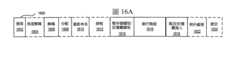
圖16A是示出依據本發明之實施例的示例性循序管線及示例性暫存器重新命名、亂序發出/執行管線二者的方塊圖;FIG. 16A is a block diagram showing both an exemplary sequential pipeline and an exemplary register renaming, out-of-order issue/execution pipeline according to an embodiment of the present invention;
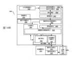
圖16B是示出依據本發明之實施例的將被包括在處理器中的循序架構核心之示例性實施例及示例性暫存器重新命名、亂序發出/執行架構核心二者的方塊圖;FIG. 16B is a block diagram showing both an exemplary embodiment of an in-order architecture core and an exemplary register renaming, out-of-order issue/execution architecture core to be included in a processor according to an embodiment of the present invention;
圖17A是依據本發明之實施例的單處理器核心、連同其至晶粒上互連網路1702的連接以及其之第2階(L2)快取1704的本地子集;FIG. 17A is a diagram of a single processor core, along with its connection to the on-die interconnect network 1702 and its local subset of the level 2 (L2)
圖17B是依據本發明之實施例的圖17A中的處理器核心之一部分的擴展視圖;FIG. 17B is an expanded view of a portion of the processor core in FIG. 17A according to an embodiment of the present invention;
圖18是依據本發明之實施例的處理器1800的方塊圖,其可具有多於一個的核心、可具有積體記憶體控制器、且可具有積體圖形;FIG. 18 is a block diagram of a
圖19示出依據本發明之一個實施例的系統的方塊圖;Figure 19 shows a block diagram of a system according to one embodiment of the present invention;
圖20是依據本發明之實施例的第一更具體的示例性系統的方塊圖;Figure 20 is a block diagram of a first more specific exemplary system according to an embodiment of the present invention;
圖21是依據本發明之實施例的第二更具體的示例性系統的方塊圖;FIG. 21 is a block diagram of a second more specific exemplary system according to an embodiment of the present invention;
圖22是依據本發明之實施例的SoC的方塊圖;以及FIG. 22 is a block diagram of a SoC according to an embodiment of the present invention; and
圖23是依據本發明之實施例的對比使用軟體指令轉換器將來源指令集中的二進制指令轉換為目標指令集中的二進制指令的方塊圖。FIG. 23 is a block diagram of using a software instruction converter to convert binary instructions in a source instruction set into binary instructions in a target instruction set according to an embodiment of the present invention.
在下面的說明中,闡述了許多具體的細節。然而,應理解的是,可在沒有這些具體細節的情況下實施本發明的實施例。在其他實例下,並未詳細地示出公知的電路、結構和技術,以免模糊對本說明書的理解。In the following description, many specific details are set forth. However, it should be understood that embodiments of the present invention may be implemented without these specific details. In other instances, well-known circuits, structures, and techniques are not shown in detail to avoid obscuring the understanding of this specification.
說明書中對「一個實施例」、「一實施例」、「一示例性實施例」等的提及表示所描述的實施例可包括特定的特徵、結構、或特性,但每個實施例可不必包括該特定的特徵、結構、或特性。而且,這樣的用語不一定指稱相同的實施例。此外,當結合一實施例描述特定的特徵、結構、或特性時,會認為結合其他實施例影響這種特徵、結構、或特性是落在本領域技術人員的知識範圍內,無論有無明確地說明。References to "one embodiment", "an embodiment", "an exemplary embodiment", etc. in the specification indicate that the described embodiment may include specific features, structures, or characteristics, but each embodiment may not necessarily include the specific features, structures, or characteristics. Moreover, such terms do not necessarily refer to the same embodiment. In addition, when a specific feature, structure, or characteristic is described in conjunction with an embodiment, it is considered that it is within the knowledge of a person skilled in the art to affect such feature, structure, or characteristic in conjunction with other embodiments, whether or not explicitly stated.
在處理大資料集時,透過將資料型態調整成盡可能的小,可增加記憶體和運算密度。若輸入項來自感測器資料,則預期會有8或16位元的整數資料作為輸入。類神經網路計算,其也可被編碼成匹配這種密集的格式,通常具有「小」數字作為輸入項。然而,累加器進行加總乘積,意味著累加器應容許兩倍的輸入項的位元數(乘法的性質)而且可能更多,以避免在計算中的任何點的溢位(overflow)或飽和(saturation)。When processing large datasets, memory and computational density can be increased by making the data types as small as possible. If the input comes from sensor data, 8 or 16-bit integer data is expected as input. Neural network computations, which can also be encoded to match this dense format, usually have "small" numbers as input. However, the accumulator sums the products, which means that the accumulator should allow twice the number of bits of the input (the nature of multiplication) and possibly more to avoid overflow or saturation at any point in the computation.
本文詳述的是,試圖在融合乘法累加(fused multiply accumulate,FMA)運算鏈中,保持輸入資料尺寸為小並且加總至較大的累加器的實施例。圖1示出依據實施例之使用不同大小的運算元的融合乘法累加指令的示例性執行。相對於儲存用於累加的全尺寸(full-size)緊縮資料元件的第三來源105(例如,單輸入、多資料(SIMD)或向量暫存器),第一來源101(例如,SIMD或向量暫存器)及第二來源103儲存「半尺寸(half-sized)」的緊縮資料元件。緊縮資料元件尺寸以此方式存在的任何一組值都是可支持的。Detailed herein is an embodiment of an attempt to keep input data sizes small and sum to a larger accumulator in a fused multiply accumulate (FMA) chain. FIG. 1 illustrates an exemplary execution of a fused multiply accumulate instruction using operands of different sizes according to an embodiment. A first source 101 (e.g., a SIMD or vector register) and a
如所示,將儲存在第一及第二來源101及103的相同位置的緊縮資料元件的值相乘。例如,A0*B0、A1*B1等等。將兩個這種「半尺寸」的緊縮資料元件的乘法結果加到來自第三來源105的對應的「全尺寸」的緊縮資料元件。例如,A0*B0+A1*B1+C0等等。As shown, the values of the packed data elements stored at the same position of the first and
將結果儲存在具有至少為「全尺寸」的緊縮資料元件尺寸的目的地107(例如,SIMD暫存器)中。在一些實施例中,第三來源105與目的地107是相同的。The result is stored in a destination 107 (e.g., a SIMD register) having a packed data element size of at least "full size". In some embodiments, the
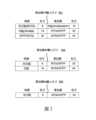
圖2示出依據實施例之2的乘冪大小的SIMD實現,其中累加器使用的輸入尺寸大於乘法器的輸入尺寸。注意,來源(至乘法器)及累加器值可以是帶正負號(signed)或者是不帶正負號(unsigned)的值。對於具有2X輸入尺寸的累加器(換句話說,累加器輸入值的尺寸是來源的緊縮資料元件尺寸的兩倍),表格201示出了不同的配置。對於位元組(byte)大小的來源,累加器使用字組(word)或者尺寸為16位元的半精度浮點數(half-precision floating-point,HPFP)值。對於字組大小的來源,累加器使用32位元整數或者尺寸為32位元的單精度浮點數(single-precision floating-point,SPFP)值。對於SPFP或32位元大小的來源,累加器使用64位元或者尺寸為64位元的雙精度浮點數(double-precision floating-point,DPFP)值。使用圖1作為範例,當來源1 101及來源2 103的緊縮資料元件尺寸為8位元時,則累加器將使用來自來源3 103的16位元大小的資料元件。當來源1 101及來源2 103的緊縮資料元件尺寸為16位元時,則累加器將使用來自來源3 103的32位元大小的資料元件。當來源1 101及來源2 103的緊縮資料元件尺寸為32位元時,則累加器將使用來自來源3 103的64位元大小的資料元件。FIG. 2 illustrates a SIMD implementation of multiplication size according to
對於具有4X輸入尺寸的累加器(換句話說,累加器輸入值的尺寸是來源的緊縮資料元件尺寸的四倍),表格203示出了不同的配置。對於位元組大小的來源,累加器使用32位元整數或者尺寸為32位元的單精度浮點數(SPFP)。對於字組大小的來源,累加器使用64位元整數或者尺寸為64位元的雙精度浮點數(DPFP)值。使用圖1作為範例,當來源1 101及來源2 103的緊縮資料元件尺寸為8位元時,則累加器將使用來自來源3 103的32位元大小的資料元件。當來源1 101及來源2 103的緊縮資料元件尺寸為16位元時,則累加器將使用來自來源3 103的64位元大小的資料元件。Table 203 shows different configurations for accumulators with 4X input size (in other words, the size of the accumulator input value is four times the size of the source's packed data element). For byte-sized sources, the accumulator uses 32-bit integers or single-precision floating point numbers (SPFP) with a size of 32 bits. For word-sized sources, the accumulator uses 64-bit integers or double-precision floating point (DPFP) values with a size of 64 bits. Using FIG. 1 as an example, when the packed data element size of
對於具有8X輸入尺寸的累加器(換句話說,累加器輸入值的尺寸是來源的緊縮資料元件尺寸的八倍),表格205示出了配置。對於位元組大小的來源,累加器使用64位元整數或者尺寸為64位元的雙精度浮點數(DPFP)值。使用圖1作為範例,當來源1 101及來源2 103的緊縮資料元件尺寸為8位元時,則累加器將使用來自來源3 103的64位元大小的資料元件。For an accumulator with an 8X input size (in other words, the size of the accumulator input value is eight times the size of the source's packed data element), Table 205 shows the configuration. For byte-sized sources, the accumulator uses 64-bit integers or double-precision floating point (DPFP) values that are 64 bits in size. Using Figure 1 as an example, when the packed data element size of
本文詳述的是用於融合乘法累加的指令及電路的實施例。在一些實施例中,融合乘法累加指令具有混合精度及/或使用水平縮減,如本文所述。Detailed herein are embodiments of instructions and circuitry for fused multiply-accumulate. In some embodiments, the fused multiply-accumulate instructions have mixed precision and/or use horizontal reduction, as described herein.
本文詳述的是指令的實施例,當該指令被執行時,針對目的地的每個緊縮資料元件位置,導致來自對應於第三來源的緊縮資料元件位置的第一及第二來源的M個N尺寸的緊縮資料元件相乘,並且將這些相乘的結果加到第三來源的緊縮資料元件位置的全尺寸的(相對於N尺寸的緊縮資料元件)緊縮資料元件,並且將相加結果儲存在對應於第三來源的緊縮資料元件位置的緊縮資料元件位置目的地中,其中M等於全尺寸的緊縮資料元件除以N。例如,當M等於2(例如,全尺寸的緊縮資料元件為16位元且N為8位元)時,將來自第一來源的連續緊縮資料元件乘以第二來源的個別的連續緊縮資料元件。Detailed herein is an embodiment of an instruction that, when executed, causes, for each packed data element location at a destination, M packed data elements of N size from a first and second source corresponding to a packed data element location of a third source to be multiplied, and the results of these multiplications to be added to the full-sized (relative to the N-sized packed data element) packed data element at the packed data element location of the third source, and the results of the addition to be stored in the packed data element location destination corresponding to the packed data element location of the third source, where M is equal to the full-sized packed data element divided by N. For example, when M is equal to 2 (e.g., the full-size packed data element is 16 bits and N is 8 bits), the continuous packed data element from the first source is multiplied by the respective continuous packed data element from the second source.
同樣的,本文詳述的是指令的實施例,當該指令被執行時,導致來自第一及第二來源的一對半尺寸的緊縮資料元件相乘,並且將這些相乘的結果加到第三來源的全尺寸的(相對於半尺寸的緊縮資料元件)緊縮資料元件,並且將結果儲存在目的地中。換句話說,在一些實施例中,針對第三來源的每個資料元件位置i,將來自第一來源的資料元件位置[2i]的資料與來自第二來源的資料元件位置[2i]的資料相乘以產生第一結果,將來自第一來源的資料元件位置[2i+1]的資料與來自第二來源的資料元件位置[2i+1]的資料相乘以產生第二結果,並且將該第一及第二結果加到來自第三來源的資料元件位置i的資料。在一些實施例中,在加法結束時執行飽和運算。在一些實施例中,在相乘之前將來自第一及/或第二來源的資料做正負號擴展。Likewise, detailed herein are embodiments of instructions that, when executed, cause a pair of half-sized packed data elements from a first and a second source to be multiplied, and the results of those multiplications to be added to full-sized (relative to half-sized packed data elements) packed data elements from a third source, and the results to be stored in a destination. In other words, in some embodiments, for each data element position i of the third source, data from data element position [2i] of the first source is multiplied with data from data element position [2i] of the second source to produce a first result, data from data element position [2i+1] of the first source is multiplied with data from data element position [2i+1] of the second source to produce a second result, and the first and second results are added to the data from data element position i of the third source. In some embodiments, a saturation operation is performed at the end of the addition. In some embodiments, the data from the first and/or second sources are sign-expanded before multiplication.
此外,本文詳述的是指令的實施例,當該指令被執行時導致來自第一及第二來源的四個(quartet)四分之一尺寸的緊縮資料元件相乘,並且將相乘的結果加到第三來源的全尺寸的(相對於四分之一尺寸的緊縮資料元件)緊縮資料元件,並且將結果儲存在目的地中。換句話說,在一些實施例中,針對第三來源的每個資料元件位置i,將來自第一來源的資料元件位置[4i]的資料與來自第二來源的資料元件位置[4i]的資料相乘以產生第一結果,將來自第一來源的資料元件位置[4i+1]的資料與來自第二來源的資料元件位置[4i+1]的資料相乘以產生第二結果,將來自第一來源的資料元件位置[4i+2]的資料與來自第二來源的資料元件位置[4i+2]的資料相乘以產生第三結果,將來自第一來源的資料元件位置[4i+3]的資料與來自第二來源的資料元件位置[4i+3]的資料相乘以產生第四結果,並且將該第一、第二、第三及第四結果加到來自第三來源的資料元件位置i的資料。在一些實施例中,在加法結束時執行飽和運算。在一些實施例中,在相乘之前將來自第一及/或第二來源的資料做正負號擴展。Additionally, described herein are embodiments of instructions that, when executed, result in multiplying four (quartet) quarter-sized packed data elements from a first and a second source, adding the result of the multiplication to a full-sized (relative to the quarter-sized packed data element) packed data element from a third source, and storing the result in a destination. In other words, in some embodiments, for each data element position i of the third source, data from data element position [4i] of the first source is multiplied with data from data element position [4i] of the second source to produce a first result, data from data element position [4i+1] of the first source is multiplied with data from data element position [4i+1] of the second source to produce a second result, data from data element position [4i+2] of the first source is multiplied with data from data element position [4i+2] of the second source to produce a third result, data from data element position [4i+3] of the first source is multiplied with data from data element position [4i+3] of the second source to produce a fourth result, and the first, second, third and fourth results are added to the data at data element position i of the third source. In some embodiments, a saturation operation is performed at the end of the addition. In some embodiments, data from the first and/or second source are sign-expanded prior to multiplication.
在一些整數版本的指令的實施例中,當加法結果的值太大時,使用飽和電路來保存運算元的正負號。特別是,飽和評估發生在介於多路加法(multi-way-add)和寫入至目的地之間的無限精度(infinite precision)結果。有些情況是,最大正數或最小負數不能被信任,因為它可能反映了計算超出容器空間。然而,這至少可以被檢查。當累加器是浮點且輸入項是整數時,則要回答的問題是如何以及何時進行整數乘積的轉換,使得從部分項到最後浮點累加不存在兩次捨入(double-rounding)。在一些實施例中,將乘積之和以及浮點累加器轉換成無限精度值(數百位元的定點數),執行相加,然後執行單次捨入到實際的累加器類型。In some implementations of the integer versions of the instructions, saturation circuitry is used to preserve the signs of the operands when the value of the addition result is too large. In particular, saturation evaluation occurs between the infinite precision result of a multi-way-add and the writing of the result to the destination. There are cases where the maximum positive or minimum negative value cannot be trusted because it may reflect a calculation that exceeded the container space. However, this can at least be checked. When the accumulator is floating point and the input terms are integers, the question to be answered is how and when to perform the conversion of the integer product so that there is no double-rounding from the partial terms to the final floating-point accumulation. In some embodiments, the sum of products and floating point accumulator are converted to infinite precision values (hundreds of bits of fixed point), the addition is performed, and then a single round is performed to the actual accumulator type.
在一些實施例中,當輸入項是浮點運算元時,捨入並且處理特殊值(無限大及非數值(NANs)),計算中錯誤的排序需要在定義中解決。在一些實施例中,模擬指定一運算順序,並保證該執行提供依該排序的錯誤。這種執行可能無法避免在計算過程中的多次捨入。單精度乘法可以完全地填入雙精度結果中,無論輸入值為何。然而,兩個這種運算的水平相加在沒有捨入的情況下可能無法填入雙精度浮點數(double),且總和在沒有額外捨入的情況下可能無法填入累加器。在一些實施例中,在水平求和期間執行捨入,並在累加期間執行一次捨入。In some embodiments, when the inputs are floating-point operands, rounding and handling of special values (infinites and non-numbers (NANs)), incorrect ordering of calculations needs to be addressed in the definition. In some embodiments, the simulation specifies an order of operations and guarantees that the implementation provides errors according to that ordering. Such an implementation may not be able to avoid multiple roundings during the calculation process. Single-precision multiplication can fill completely into the double-precision result, regardless of the input values. However, the horizontal addition of two such operations may not fit into a double without rounding, and the sum may not fit into the accumulator without additional rounding. In some embodiments, rounding is performed during horizontal summation and once during accumulation.
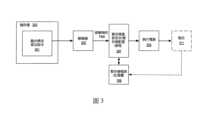
圖3示出用以處理諸如融合乘法累加指令之指令的硬體的實施例。如所示,儲存器303儲存待執行的融合乘法累加指令301,針對目的地的每個緊縮資料元件位置,導致來自對應於第三來源的緊縮資料元件位置的第一及第二來源的M個N尺寸的緊縮資料元件相乘,將這些相乘的結果加到第三來源的緊縮資料元件位置的全尺寸的(相對於N尺寸的緊縮資料元件)緊縮資料元件,並且將相加結果儲存在對應於第三來源的緊縮資料元件位置的緊縮資料元件位置目的地中,其中M等於全尺寸的緊縮資料元件除以N。FIG3 illustrates an embodiment of hardware for processing instructions such as fused multiply-accumulate instructions. As shown, register 303 stores a fused multiply-accumulate instruction 301 to be executed, causing, for each packed data element position of a destination, M packed data elements of size N from the first and second sources corresponding to the packed data element position of a third source to be multiplied, adding the results of these multiplications to the full-sized (relative to the packed data element of size N) packed data elements of the packed data element position of the third source, and storing the addition results in the packed data element position destination corresponding to the packed data element position of the third source, where M is equal to the full-sized packed data element divided by N.
指令301由解碼電路305接收。例如,解碼電路305從提取邏輯/電路接收此指令。該指令包括第一、第二和第三來源以及目的地的欄位。在一些實施例中,來源和目的地是暫存器。此外,在一些實施例中,第三來源和目的地是相同的。指令301的運算碼及/或前綴(prefix)包括位元組(byte)、字組(word)、雙字組(doubleword)、及四字組(quadword)之來源和目的地資料元件尺寸{B/W/D/Q}的指示,以及迭代次數。Instruction 301 is received by decode circuit 305. For example, decode circuit 305 receives this instruction from extraction logic/circuitry. The instruction includes fields for first, second, and third sources and destinations. In some embodiments, the sources and destinations are registers. Furthermore, in some embodiments, the third source and destination are the same. The operation code and/or prefix of instruction 301 includes an indication of the source and destination data element size {B/W/D/Q} of byte, word, doubleword, and quadword, and the number of iterations.
將於後面詳述至少一個指令格式的更詳細的實施例。解碼電路305將指令解碼成一或多個運算。在一些實施例中,此解碼包括產生將由執行電路(諸如執行電路309)執行的複數個微運算。解碼電路305也解碼指令前綴。More detailed embodiments of at least one instruction format will be described in detail below. Decoding circuit 305 decodes the instruction into one or more operations. In some embodiments, this decoding includes generating a plurality of micro-operations to be executed by an execution circuit (such as execution circuit 309). Decoding circuit 305 also decodes the instruction prefix.
在一些實施例中,暫存器重新命名、暫存器配置、及/或排程電路307提供以下一或多項功能:(1)將邏輯運算元值重新命名為實體運算元值(例如,在一些實施例中為暫存器別名表),(2)將狀態位元和旗標分配給經解碼的指令;以及(3)排程經解碼的指令用於在指令池之外的執行電路上執行(例如,在一些實施例中使用保留站(reservation station))。暫存器(暫存器檔案)及/或記憶體308將資料儲存為將由執行電路309運算的指令的運算元。示例性暫存器類型包括緊縮資料暫存器、通用暫存器和浮點暫存器。In some embodiments, register renaming, register allocation, and/or
執行電路309執行經解碼的指令。The
在一些實施例中,引退/寫回電路311在架構上將目的地暫存器提交到暫存器或記憶體中,並且引退指令。In some embodiments, the retire/
融合乘法累加指令之格式的一實施例為FMA[SOURCESIZE{B/W/D/Q}][DESTSIZE{B/W/D/Q}]DSTREG,SRC1,SRC2,SRC3。在一些實施例中,FMA[SOURCESIZE{B/W/D/Q}][DESTSIZE{B/W/D/Q}]是指令的運算碼及/或前綴。B/W/D/Q指示來源/目的地的資料元件尺寸為位元組、字組、雙字組、及四字組。DSTREG是緊縮資料目的地暫存器運算元的欄位。SRC1、SRC2、及SRC3是諸如緊縮資料暫存器及/或記憶體等來源的欄位。An embodiment of the format of the fused multiply-accumulate instruction is FMA[SOURCESIZE{B/W/D/Q}][DESTSIZE{B/W/D/Q}]DSTREG,SRC1,SRC2,SRC3. In some embodiments, FMA[SOURCESIZE{B/W/D/Q}][DESTSIZE{B/W/D/Q}] is the opcode and/or prefix of the instruction. B/W/D/Q indicates the source/destination data element size as byte, word, double word, and quad word. DSTREG is a field of the packed data destination register operand. SRC1, SRC2, and SRC3 are fields of sources such as packed data registers and/or memory.
融合乘法累加指令之格式的一實施例為FMA[SOURCESIZE{B/W/D/Q}][DESTSIZE{B/W/D/Q}]DSTREG/SRC3,SRC1,SRC2。在一些實施例中,FMA[SOURCESIZE{B/W/D/Q}][DESTSIZE{B/W/D/Q}]是指令的運算碼及/或前綴。B/W/D/Q指示來源/目的地的資料元件尺寸為位元組、字組、雙字組、及四字組。DSTREG/SRC3是緊縮資料目的地暫存器運算元及第三來源運算元的欄位。SRC1及SRC2是諸如緊縮資料暫存器及/或記憶體等來源的欄位。An embodiment of the format of the fused multiply-accumulate instruction is FMA[SOURCESIZE{B/W/D/Q}][DESTSIZE{B/W/D/Q}]DSTREG/SRC3,SRC1,SRC2. In some embodiments, FMA[SOURCESIZE{B/W/D/Q}][DESTSIZE{B/W/D/Q}] is the operand and/or prefix of the instruction. B/W/D/Q indicates the source/destination data element size as byte, word, double word, and quad word. DSTREG/SRC3 is the field of the packed data destination register operand and the third source operand. SRC1 and SRC2 are fields of sources such as packed data registers and/or memory.
在一些實施例中,融合乘法累加指令包括writemask(寫入遮罩)暫存器運算元(k)的欄位(例如,FMA[SOURCESIZE{B/W/D/Q}][DESTSIZE{B/W/D/Q}]{k}DSTREG/SRC3,SRC1,SRC2或FMA[SOURCESIZE{B/W/D/Q}][DESTSIZE{B/W/D/Q}]{k}DSTREG,SRC1,SRC2,SRC3)。寫入遮罩被用來有條件地控制每個元件的運算和更新結果。取決於實作,寫入遮罩使用合併(merging)或歸零(zeroing)遮蔽。以述詞(predicate)(writemask、寫入遮罩、或k暫存器)運算元編碼的指令使用該運算元來有條件地控制每個元件的運算操作並且將結果更新到目的地運算元。述詞運算元被稱為opmask(寫入遮罩)暫存器。opmask是一組尺寸為MAX_KL(64位元)的架構暫存器。應注意的是,從這組架構暫存器,只有k1到k7可被定址為述詞運算元。k0可被用作正規的來源或目的地,但不可被編碼為述詞運算元。亦應注意的是,述詞運算元可被用來針對具有記憶體運算元(來源或目的地)的一些指令啟用記憶體故障抑制。作為述詞運算元,opmask暫存器包含一個位元,用來管理對向量暫存器的每個資料元件的運算/更新。一般來說,opmask暫存器可支援具有下列元件尺寸的指令:單精度浮點數(float32)、整數雙字組(int32)、雙精度浮點數(float64)、整數四字組(int64)。opmask暫存器的長度MAX_KL足以處理多達64個元件,每個元件一個位元,亦即64位元。對於給定的向量長度,每個指令僅存取依照其資料類型所需的最低有效遮罩位元數。opmask暫存器以每元件的粒度影響指令。因此,在opmask暫存器的對應位元上斷定每個資料元件的任意數值或非數值運算以及至目的地運算元的中間結果的每元件更新。在大部分的實施例中,作為述詞運算元的opmask遵守下列屬性:(1)對於未設定對應的opmask位元的元件,不執行指令的運算(這意味著對於未遮蔽(masked-off)元件的運算不會引起例外(exception)或違規(violation),並且因此,由於未遮蔽運算,沒有例外旗標被更新);(2)若未設定對應的寫入遮罩位元,則不會以運算結果來更新目的地元件,而是,必須保存目的地元件值(合併遮蔽)或者必須將目的地元件值歸零(歸零遮蔽);(3)針對具有記憶體運算元的一些指令,對於具有遮罩位元為0的元件,抑制記憶體故障。應注意的是,此特性提供了一通用結構來實現控制流程斷定,因為遮罩實際上為向量暫存器目的地提供了合併行為。作為替代,遮罩可被用於歸零而非合併,因而,以0來更新被遮蔽掉的元件,而不是保留舊值。歸零行為被提供來在不需要舊值的隱含相依性時將其移除。In some embodiments, the fused multiply-accumulate instruction includes a writemask register field for operand (k) (e.g., FMA[SOURCESIZE{B/W/D/Q}][DESTSIZE{B/W/D/Q}]{k}DSTREG/SRC3,SRC1,SRC2 or FMA[SOURCESIZE{B/W/D/Q}][DESTSIZE{B/W/D/Q}]{k}DSTREG,SRC1,SRC2,SRC3). The writemask is used to conditionally control the operation and update results of each element. Depending on the implementation, the writemask uses merging or zeroing masking. Instructions encoded with a predicate (writemask, write mask, or k register) operand use the operand to conditionally control the operation of each element and update the result to the destination operand. The predicate operand is called the opmask (write mask) register. The opmask is a set of architectural registers of size MAX_KL (64 bits). It should be noted that from this set of architectural registers, only k1 to k7 can be addressed as predicate operands. k0 can be used as a regular source or destination, but cannot be encoded as a predicate operand. It should also be noted that the predicate operand can be used to enable memory fault suppression for some instructions with memory operands (source or destination). As a predicate operand, the opmask register contains one bit that manages operations/updates on each data element of the vector register. In general, the opmask register supports instructions with the following element sizes: single precision floating point (float32), integer double word (int32), double precision floating point (float64), integer quadword (int64). The length MAX_KL of the opmask register is sufficient to handle up to 64 elements, one bit per element, or 64 bits. For a given vector length, each instruction accesses only the least significant number of mask bits required for its data type. The opmask register affects instructions at a per-element granularity. Therefore, any numeric or non-numeric operation on each data element and any per-element update of the intermediate result to the destination operand are asserted on the corresponding bit of the opmask register. In most embodiments, opmask as a predicate operand observes the following properties: (1) for elements for which the corresponding opmask bit is not set, the instruction's operation is not performed (this means that the operation on an unmasked-off element will not cause an exception or violation, and therefore, no exception flags are updated due to the unmasked operation); (2) if the corresponding write mask bit is not set, the destination element is not updated with the operation result, but instead, the destination element value must be saved (merge mask) or the destination element value must be zeroed (zero mask); (3) for some instructions with memory operands, memory faults are suppressed for elements with mask bits set to 0. It should be noted that this feature provides a general construct to implement control flow assertions, since masks actually provide merge behavior for vector register destinations. Alternatively, masks can be used for zeroing rather than merging, thus updating the masked out elements with 0 rather than retaining the old value. Zeroing behavior is provided to remove implicit dependencies on old values when they are not needed.
在實施例中,指令的編碼包括縮放-索引-基底(scale-index-base)(SIB)類型的記憶體尋址運算元,其間接地識別記憶體中的多個索引目的地位置。在一個實施例中,SIB類型記憶體運算元可包括識別基址暫存器的編碼。基址暫存器的內容可表示記憶體中的基底位址,從該基底位址可計算記憶體中的特定目的地位置的位址。例如,基底位址可以是擴展向量指令之潛在目的地位置的方塊中的第一位置的位址。在一個實施例中,SIB類型的記憶體運算元可包括識別索引暫存器的編碼。索引暫存器的每個元件可指定一索引或偏移(offset)值,其可用來從基底位址計算在潛在目的地位置的方塊內的個別目的地位置的位址。在一個實施例中,SIB類型的記憶體運算元可包括指定縮放因子的編碼,當計算個別目的地位址時,該縮放因子被施加到每個索引值。例如,若在SIB類型的記憶體運算元中編碼縮放因子值為4,則從索引暫存器獲得的每個索引值可被乘以4,接著被加到基底位址來計算目的地位址。In an embodiment, the encoding of the instruction includes a scale-index-base (SIB) type memory addressing operator that indirectly identifies multiple indexed destination locations in memory. In one embodiment, the SIB type memory operator may include an encoding that identifies a base address register. The contents of the base address register may represent a base address in memory from which the address of a specific destination location in memory can be calculated. For example, the base address may be the address of the first position in a block of potential destination locations for an expand vector instruction. In one embodiment, the SIB type memory operator may include an encoding that identifies an index register. Each element of the index register may specify an index or offset value that may be used to calculate the address of a respective destination location within a block of potential destination locations from a base address. In one embodiment, a SIB-type memory operator may include an encoding that specifies a scaling factor that is applied to each index value when calculating the respective destination address. For example, if a scaling factor value of 4 is encoded in a SIB-type memory operator, each index value obtained from the index register may be multiplied by 4 and then added to the base address to calculate the destination address.
在一個實施例中,具有vm32{x,y,z}形式的SIB類型的記憶體運算元可識別使用SIB類型的記憶體尋址來指定的記憶體運算元的向量陣列。在此範例中,使用共同基底(common base)暫存器、常數縮放因子、以及包含每個單獨元件為32位元索引值之多個單獨元件的向量索引暫存器來指定記憶體位址的陣列。向量索引暫存器可以是XMM暫存器(vm32x)、YMM暫存器(vm32y)、或ZMM暫存器(vm32z)。在另一實施例中,具有vm64{x,y,z}形式的SIB類型的記憶體運算元可識別使用SIB類型的記憶體尋址來指定記憶體運算元的向量陣列。在此範例中,使用共同基底暫存器、常數縮放因子、以及包含每個單獨元件為64位元索引值之多個單獨元件的向量索引暫存器來指定記憶體位址的陣列。向量索引暫存器可以是XMM暫存器(vm64x)、YMM暫存器(vm64y)、或ZMM暫存器(vm64z)。In one embodiment, a memory operand with a SIB type of the form vm32{x,y,z} may identify a vector array of memory operands specified using SIB type memory addressing. In this example, a common base register, a constant scaling factor, and a vector index register containing multiple individual elements with each individual element being a 32-bit index value are used to specify the array of memory addresses. The vector index register may be an XMM register (vm32x), a YMM register (vm32y), or a ZMM register (vm32z). In another embodiment, a memory operand having a SIB type of the form vm64{x,y,z} may identify a vector array that uses SIB type memory addressing to specify the memory operand. In this example, a common base register, a constant scaling factor, and a vector index register containing multiple individual elements, each of which is a 64-bit index value, are used to specify the array of memory addresses. The vector index register may be an XMM register (vm64x), a YMM register (vm64y), or a ZMM register (vm64z).
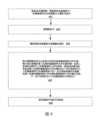
圖4示出由處理器執行以處理融合乘法累加指令的方法的實施例。FIG4 illustrates an embodiment of a method executed by a processor to process a fused multiply-accumulate instruction.
在401,提取指令。例如,提取融合乘法累加指令。融合乘法累加指令包括運算碼、以及緊縮資料來源運算元和緊縮資料目的地運算元的欄位,如上所詳述的。在一些實施例中,融合乘法累加指令包括寫入遮罩運算元。在一些實施例中,從指令快取提取指令。At 401, an instruction is retrieved. For example, a fused multiply-accumulate instruction is retrieved. The fused multiply-accumulate instruction includes an operand, and fields for a packed data source operand and a packed data destination operand, as described in detail above. In some embodiments, the fused multiply-accumulate instruction includes a write mask operand. In some embodiments, the instruction is retrieved from an instruction cache.
在403解碼該提取的指令。例如,由解碼電路解碼該提取的融合乘法累加指令,如此處所詳述的。The extracted instruction is decoded at 403. For example, the extracted fused multiply-accumulate instruction is decoded by a decode circuit, as described in detail herein.
在405擷取與經解碼的指令的來源運算元相關聯的資料值。At 405, the data value associated with the source operand of the decoded instruction is retrieved.
在407,由執行電路(硬體)執行經解碼的指令,如此處所詳述的。針對融合乘法累加指令,該執行將針對目的地的每個緊縮資料元件位置,導致來自對應於第三來源的緊縮資料元件位置的第一及第二來源的M個N尺寸的緊縮資料元件的相乘,將這些相乘的結果加到第三來源的緊縮資料元件位置的全尺寸的(相對於N尺寸的緊縮資料元件)緊縮資料元件,並且將相加結果儲存在對應於第三來源的緊縮資料元件位置的緊縮資料元件位置目的地中,其中M等於全尺寸的緊縮資料元件除以N。At 407, the decoded instruction is executed by execution circuitry (hardware) as described in detail herein. For a fused multiply-accumulate instruction, the execution will result in, for each packed data element location at the destination, a multiplication of M N-sized packed data elements from the first and second sources corresponding to the packed data element location of the third source, adding the results of these multiplications to the full-sized (relative to the N-sized packed data element) packed data element at the packed data element location of the third source, and storing the results of the addition in the packed data element location destination corresponding to the packed data element location of the third source, where M equals the full-sized packed data element divided by N.
在一些實施例中,在409提交(commit)或引退(retire)指令。In some embodiments, the instruction is committed or retired at 409.
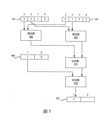
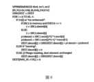
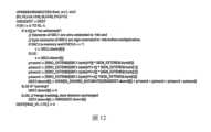
圖5示出融合乘法累加之執行的子集的實施例。特別是,這示出了目的地的一個緊縮資料元件位置的迭代的執行電路。在此實施例中,對帶正負號的來源進行融合乘法累加,其中累加器是輸入資料尺寸的2倍。圖6示出用於在硬體中執行此指令的虛擬碼的實施例。FIG5 shows an embodiment of a subset of the execution of a fused multiply-accumulate. In particular, this shows the execution circuit for an iteration of a packed data element location of the destination. In this embodiment, a fused multiply-accumulate is performed on signed sources, where the accumulator is twice the size of the input data. FIG6 shows an embodiment of the virtual code for executing this instruction in hardware.
第一帶正負號的來源(來源1 501)及第二帶正負號的來源(來源2 503)各具有四個緊縮資料元件。這些緊縮資料元件之各者儲存諸如浮點數資料的帶正負號的資料。第三帶正負號的來源509(來源3)具有兩個緊縮資料元件,其之各者儲存帶正負號的資料。第一及第二帶正負號的來源501及503的尺寸第三帶正負號的來源509的尺寸的一半。例如,第一及第二帶正負號的來源501及503可具有32位元的緊縮資料元件(例如,單精度浮點數),第三帶正負號的來源509可具有64位元的緊縮資料元件(例如,雙精度浮點數)。The first signed source (
在此圖示中,僅示出第一及第二帶正負號的來源501及503的兩個最高有效(most significant)緊縮資料元件位置和第三帶正負號的來源509的最高有效緊縮資料元件位置。當然,其他的緊縮資料元件位置也會被處理。In this illustration, only the two most significant compressed data component positions of the first and second signed
如所示,以成對的方式處理緊縮資料元件。例如,使用乘法器電路505將第一及第二帶正負號的來源501及503的最高有效緊縮資料元件位置的資料相乘,並且使用乘法器電路507將來自第一及第二帶正負號的來源501及503的第二最高有效緊縮資料元件位置的資料相乘。在一些實施例中,這些乘法器電路505及507被重複用於其他的緊縮資料元件位置。在其他實施例中,使用附加的乘法器電路,使得緊縮資料元件被平行處理。在一些情況下,平行執行是使用帶正負號的第三來源509的尺寸的通道完成的。使用加法電路511將每個相乘的結果相加。As shown, the packed data elements are processed in pairs. For example, data from the most significant packed data element positions of the first and second signed
乘法結果的相加結果被加到來自帶正負號的來源3 509的最高有效緊縮資料元件位置的資料(使用不同的加法器513或相同的加法器511)。The addition result of the multiplication result is added to the data from the most significant packed data element position from signed
最後,將第二加法的結果儲存到對應於帶正負號的第三來源509所使用的緊縮資料元件位置的緊縮資料元件位置中的帶正負號的目的地515。在一些實施例中,將寫入遮罩應用於此儲存器,使得若設定了對應的寫入遮罩(位元),則發生儲存,並且若未設定,則不發生儲存。Finally, the result of the second addition is stored to the signed
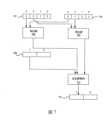
圖7示出融合乘法累加之執行的子集的實施例。特別是,這示出了目的地的一個緊縮資料元件位置的迭代的執行電路。在此實施例中,對帶正負號的來源進行融合乘法累加,其中累加器是輸入資料尺寸的2倍。圖8示出用於在硬體中執行此指令的虛擬碼的實施例。FIG7 shows an embodiment of a subset of the execution of a fused multiply-accumulate. In particular, this shows the execution circuit for an iteration of a packed data element location of the destination. In this embodiment, a fused multiply-accumulate is performed on signed sources, where the accumulator is twice the size of the input data.FIG8 shows an embodiment of the virtual code for executing this instruction in hardware.
第一帶正負號的來源(來源1 701)及第二帶正負號的來源(來源2 703)各具有四個緊縮資料元件。這些緊縮資料元件之各者儲存諸如整數資料的帶正負號的資料。第三帶正負號的來源709(來源3)具有兩個緊縮資料元件,其之各者儲存帶正負號的資料。第一及第二正負號的來源701及703的尺寸是第三帶正負號的來源709的尺寸的一半。例如,第一及第二正負號的來源701及703可具有32位元的緊縮資料元件(例如,單精度浮點數),第三帶正負號的來源709可具有64位元的緊縮資料元件(例如,雙精度浮點數)。The first signed source (
在此圖示中,僅示出第一及第二正負號的來源701及703的兩個最高有效緊縮資料元件位置和第三帶正負號的來源709的最高有效緊縮資料元件位置。當然,其他的緊縮資料元件位置也會被處理。In this illustration, only the two most significant compressed data element positions of the first and second signed
如所示,以成對的方式處理緊縮資料元件。例如,使用乘法器電路705將第一及第二正負號的來源701及703的最高有效緊縮資料元件位置的資料相乘,並且使用乘法器電路707將來自第一及第二正負號的來源701及703的第二最高有效緊縮資料元件位置的資料相乘。在一些實施例中,這些乘法器電路705及707被重複用於其他的緊縮資料元件位置。在其他實施例中,使用附加的乘法器電路,使得緊縮資料元件被平行處理。在一些情況下,平行執行是使用帶正負號的第三來源709的尺寸的通道完成的。使用加法/飽和電路711將每個相乘的結果加到帶正負號的第三來源709。As shown, the packed data elements are processed in pairs. For example, data from the most significant packed data element position of the first and second signed
加法/飽和(累加器)電路711會在加法造成值太大時保存運算元的正負號。特別是,飽和評估發生在多路加法(multi-way-add)和寫入到帶正負號的目的地715之間的無限精度的結果上。當累加器711是浮點而輸入項是整數時,將乘積之和以及浮點累加器輸入值轉換成無限精度值(數百位元的定點數),執行乘法結果和第三輸入的相加,並執行單次捨入到實際的累加器類型。Addition/saturation (accumulator)
將加法及飽和檢查的結果儲存到對應於帶正負號的第三來源709所使用的緊縮資料元件位置的緊縮資料元件位置中的帶正負號的目的地715。在一些實施例中,將寫入遮罩應用於此儲存器,使得若設定了對應的寫入遮罩(位元),則發生儲存,並且,若未設定,則不發生儲存。The result of the addition and saturation check is stored to a signed
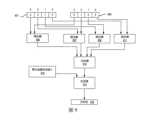
圖9示出融合乘法累加之執行的子集的實施例。特別是,這示出了目的地的一個緊縮資料元件位置的迭代的執行電路。在此實施例中,對帶正負號的來源以及不帶正負號的來源進行融合乘法累加,其中累加器是輸入資料尺寸的4倍。圖10示出用於在硬體中執行此指令的虛擬碼的實施例。Figure 9 shows an embodiment of a subset of the execution of a fused multiply-accumulate. In particular, this shows the execution circuit for an iteration of a packed data element location of the destination. In this embodiment, a fused multiply-accumulate is performed on signed sources as well as unsigned sources, where the accumulator is 4 times the size of the input data. Figure 10 shows an embodiment of the dummy code for executing this instruction in hardware.
第一帶正負號的來源(來源1 901)及第二不帶正負號的來源(來源2 903)各具有四個緊縮資料元件。這些緊縮資料元件之各者儲存諸如浮點數或整數資料的資料。第三帶正負號的來源(來源3 915)具有一緊縮資料元件,其儲存帶正負號的資料。第一及第二來源901及903的尺寸是第三帶正負號的來源915的尺寸的四分之一。例如,第一及第二來源901及903可具有16位元的緊縮資料元件(例如,字組),而第三帶正負號的來源915可具有64位元的緊縮資料元件(例如,雙精度浮點數或64位元整數)。The first signed source (
在此圖示中,示出第一及第二來源901及903的四個最高有效緊縮資料元件位置和第三帶正負號的來源915的最高有效緊縮資料元件位置。當然,如果有其他的緊縮資料元件位置,其他的緊縮資料元件位置也會被處理。In this diagram, the four most significant compressed data element positions of the first and
如所示,以四個一組的方式處理緊縮資料元件。例如,使用乘法器電路905將第一及第二來源901及903的最高有效緊縮資料元件位置的資料相乘、使用乘法器電路907將來自第一及第二來源901及903的第二最高有效緊縮資料元件位置的資料相乘、使用乘法器電路909將來自第一及第二來源901及903的第三最高有效緊縮資料元件位置的資料相乘、以及使用乘法器電路911將來自第一及第二來源901及903的最低有效緊縮資料元件位置的資料相乘。在一些實施例中,在相乘之前,將第一來源901的帶正負號的緊縮資料元件做正負號擴展(sign extended),以及將第二來源903的不帶正負號的緊縮資料元件以零擴展(zero extended)。As shown, the packed data elements are processed in groups of four. For example, data from the most significant packed data element positions of the first and
在一些實施例中,這些乘法器電路905-911被重複用於其他的緊縮資料元件位置。在其他實施例中,使用附加的乘法器電路,使得緊縮資料元件被平行處理。在一些情況下,平行執行是使用帶正負號的第三來源915的尺寸的通道完成的。使用加法電路912將每個相乘的結果相加。In some embodiments, these multiplier circuits 905-911 are repeated for other packed data element locations. In other embodiments, additional multiplier circuits are used so that packed data elements are processed in parallel. In some cases, parallel execution is accomplished using channels of the size of the
乘法結果的相加結果被加到來自帶正負號的來源3 915的最高有效緊縮資料元件位置的資料(使用不同的加法器913或相同的加法器912)。The addition result of the multiplication results is added to the data from the most significant packed data element position from signed
最後,將第二加法的結果儲存到對應於帶正負號的第三來源909所使用的緊縮資料元件位置的緊縮資料元件位置中的帶正負號的目的地919。在一些實施例中,將寫入遮罩應用於此儲存器,使得若設定了對應的寫入遮罩(位元),則發生儲存,並且,若未設定,則不發生儲存。Finally, the result of the second addition is stored to the signed destination 919 in a packed data element location corresponding to the packed data element location used by the signed
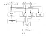
圖11示出融合乘法累加之執行的子集的實施例。特別是,這示出了目的地的一個緊縮資料元件位置的迭代的執行電路。在此實施例中,對帶正負號的來源以及不帶正負號的來源進行融合乘法累加,其中累加器是輸入資料尺寸的4倍。圖12示出用於在硬體中執行此指令的虛擬碼的實施例。FIG11 shows an embodiment of a subset of the execution of a fused multiply-accumulate. In particular, this shows the execution circuit for an iteration of a packed data element location of the destination. In this embodiment, a fused multiply-accumulate is performed on signed sources as well as unsigned sources, where the accumulator is 4 times the size of the input data. FIG12 shows an embodiment of the dummy code for executing this instruction in hardware.
第一帶正負號的來源(來源1 1101)及第二不帶正負號的來源(來源2 1103)各具有四個緊縮資料元件。這些緊縮資料元件之各者儲存諸如浮點數或整數資料的資料。第三帶正負號的來源(來源3 1115)具有一緊縮資料元件,其儲存帶正負號的資料。第一及第二來源1101及1103的尺寸是第三帶正負號的來源1115的尺寸的四分之一。例如,第一及第二來源1101及1103可具有16位元的緊縮資料元件(例如,字組),而第三帶正負號的來源1115可具有64位元的緊縮資料元件(例如,雙精度浮點數或64位元整數)。The first signed source (
在此圖示中,示出第一及第二來源1101及1103的四個最高有效緊縮資料元件位置以及第三帶正負號的來源1115的最高有效緊縮資料元件位置。當然,如果有其他的緊縮資料元件位置,其他的緊縮資料元件位置也會被處理。In this diagram, the four most significant compressed data element positions of the first and
如所示,以四個一組的方式處理緊縮資料元件。例如,使用乘法器電路1105將第一及第二來源1101及1103的最高有效緊縮資料元件位置的資料相乘、使用乘法器電路1107將來自第一及第二來源1101及1103的第二最高有效緊縮資料元件位置的資料相乘、使用乘法器電路1109將來自第一及第二來源1101及1103的第三最高有效緊縮資料元件位置的資料相乘、以及使用乘法器電路1111將來自第一及第二來源1101及1103的最低有效緊縮資料元件位置的資料相乘。在一些實施例中,在相乘之前,將第一來源1101的帶正負號的緊縮資料元件做正負號擴展,以及將第二來源1103的不帶正負號的緊縮資料元件以零擴展。As shown, the packed data elements are processed in groups of four. For example, data from the most significant packed data element positions of the first and
在一些實施例中,乘法器電路1105-1111被重複用於其他的緊縮資料元件位置。在其他實施例中,使用附加的乘法器電路,使得緊縮資料元件被平行處理。在一些情況下,平行執行是使用帶正負號的第三來源1115的尺寸的通道完成的。使用加法/飽和電路1113將每個相乘的結果加到帶正負號的第三來源1115。In some embodiments, multiplier circuits 1105-1111 are reused for other packed data element locations. In other embodiments, additional multiplier circuits are used so that packed data elements are processed in parallel. In some cases, parallel execution is accomplished using channels of the size of the signed
加法/飽和(累加器)電路1113會在加法造成值太大時保存運算元的正負號。特別是,飽和評估發生在多路加法和寫入到目的地1119之間的無限精度的結果上。當累加器1113是浮點而輸入項是整數時,將乘積之和以及浮點累加器輸入值轉換成無限精度值(數百位元的定點數),執行乘法結果和第三輸入的相加,並執行單次捨入到實際的累加器類型。Addition/saturation (accumulator)
將加法及飽和檢查的結果儲存到對應於帶正負號的第三來源1115所使用的緊縮資料元件位置的緊縮資料元件位置中的帶正負號的目的地1119。在一些實施例中,將寫入遮罩應用於此儲存器,使得若設定了對應的寫入遮罩(位元),則發生儲存,並且,若未設定,則不發生儲存。The result of the addition and saturation check is stored to a signed destination 1119 in a packed data element location corresponding to the packed data element location used by the signed
下面的附圖詳細描述實現上述實施例地示例性架構和系統。在一些實施例中,上面描述的一或多個硬體元件及/或指令被如下所述地仿真,或被實作為軟體模組。The following figures describe in detail exemplary architectures and systems for implementing the above embodiments. In some embodiments, one or more hardware components and/or instructions described above are simulated as described below, or implemented as software modules.
示例性實施例包括處理器,其包含解碼器,用以解碼單一指令,該單一指令具有運算碼、表示目的地運算元的目的地欄位、及第一、第二及第三緊縮資料來源運算元的欄位,其中第一及第二緊縮資料來源運算元的緊縮資料元件具有第一尺寸,其與第三緊縮資料運算元的緊縮資料元件的第二尺寸不同;暫存器檔案,具有複數個緊縮資料暫存器,其包括用於來源及目的地運算元的暫存器;以及執行電路,用以執行經解碼的單一指令來針對目的地運算元的每個緊縮資料元件位置,執行來自對應於第三緊縮資料來源的緊縮資料元件位置的第一及第二緊縮資料來源的M個N尺寸的緊縮資料元件的相乘,將這些相乘的結果加到第三緊縮資料來源的緊縮資料元件位置的全尺寸的緊縮資料元件,並且將相加結果儲存在對應於第三緊縮資料來源的緊縮資料元件位置的緊縮資料元件位置目的地中,其中M等於全尺寸的緊縮資料元件除以N。An exemplary embodiment includes a processor including a decoder for decoding a single instruction having an operand, a destination field representing a destination operand, and fields for first, second, and third packed data source operands, wherein packed data elements of the first and second packed data source operands have a first size that is different from a second size of packed data elements of the third packed data operand; a register file having a plurality of packed data registers including registers for source and destination operands; and an execution circuit for executing the operation. A single instruction decoded to perform, for each packed data element position of the destination operand, multiplications of M packed data elements of size N from the first and second packed data sources corresponding to the packed data element position of the third packed data source, add the results of these multiplications to the full-sized packed data element at the packed data element position of the third packed data source, and store the results of the additions in the packed data element position destination corresponding to the packed data element position of the third packed data source, where M is equal to the full-sized packed data element divided by N.
在一些實施例中,下列的一或多者適用:該指令定義該些緊縮資料元件的尺寸;在相乘之前,該執行電路以零擴展該第二來源的緊縮資料元件,以及將該第一來源的緊縮資料元件做正負號擴展;當該第一尺寸是該第二尺寸的一半時,對每個乘法執行第一相加,並且對該第一相加的結果和來自先前迭代的結果執行第二相加;當該第一尺寸是該第二尺寸的一半時,對該些乘法之各者和來自先前迭代的結果執行單次加法與飽和檢查;當該第一尺寸是該第二尺寸的四分之一時,對每個乘法執行第一相加,並且對該第一相加的結果和來自先前迭代的結果執行第二相加;及/或當該第一尺寸是該第二尺寸的四分之一時,對該些乘法之各者和來自先前迭代的結果執行單次加法與飽和檢查。In some embodiments, one or more of the following applies: the instruction defines the size of the packed data elements; the execution circuitry zero-extends the packed data elements of the second source and sign-extends the packed data elements of the first source before multiplication; when the first size is half the second size, a first addition is performed for each multiplication and a second addition is performed on the result of the first addition and the result from the previous iteration; when the first size is the When the first size is half the second size, a single addition and saturation check are performed on each of the multiplications and the result from the previous iteration; when the first size is one quarter the second size, a first addition is performed on each multiplication and a second addition is performed on the result of the first addition and the result from the previous iteration; and/or when the first size is one quarter the second size, a single addition and saturation check are performed on each of the multiplications and the result from the previous iteration.
示例性實施例包括一種解碼單一指令的方法,該單一指令具有運算碼、表示目的地運算元的目的地欄位、和第一、第二及第三緊縮資料來源運算元的欄位,其中第一及第二緊縮資料來源運算元的緊縮資料元件具有第一尺寸,其與第三緊縮資料運算元的緊縮資料元件的第二尺寸不同;暫存器檔案,具有複數個緊縮資料暫存器,其包括用於來源及目的地運算元的暫存器;以及執行經解碼的單一指令來針對目的地運算元的每個緊縮資料元件位置,執行來自對應於第三緊縮資料來源的緊縮資料元件位置的第一及第二緊縮資料來源的M個N尺寸的緊縮資料元件的相乘,將這些相乘的結果加到第三緊縮資料來源的緊縮資料元件位置的全尺寸的緊縮資料元件,並且將相加結果儲存在對應於第三緊縮資料來源的緊縮資料元件位置的緊縮資料元件位置目的地中,其中M等於全尺寸的緊縮資料元件除以N。Exemplary embodiments include a method of decoding a single instruction having an operand, a destination field representing a destination operand, and fields of first, second, and third packed data source operands, wherein packed data elements of the first and second packed data source operands have a first size that is different from a second size of packed data elements of the third packed data operand; a register file having a plurality of packed data registers including registers for source and destination operands; and executing the decoded single instruction to For each packed data element position of the destination operand, perform multiplication of M packed data elements of size N from the first and second packed data sources corresponding to the packed data element position of the third packed data source, add the results of these multiplications to the full-size packed data element of the packed data element position of the third packed data source, and store the addition results in the packed data element position destination corresponding to the packed data element position of the third packed data source, where M is equal to the full-size packed data element divided by N.
在一些實施例中,下列的一或多者適用:該指令定義該些緊縮資料元件的尺寸;在相乘之前,該執行電路以零擴展該第二來源的緊縮資料元件,以及將該第一來源的緊縮資料元件做正負號擴展;當該第一尺寸是該第二尺寸的一半時,對每個乘法執行第一相加,並且對該第一相加的結果和來自先前迭代的結果執行第二相加;當該第一尺寸是該第二尺寸的一半時,對該些乘法之各者和來自先前迭代的結果執行單次加法與飽和檢查;當該第一尺寸是該第二尺寸的四分之一時,對每個乘法執行第一相加,並且對該第一相加的結果和來自先前迭代的結果執行第二相加;及/或當該第一尺寸是該第二尺寸的四分之一時,對該些乘法之各者和來自先前迭代的結果執行單次加法與飽和檢查。In some embodiments, one or more of the following applies: the instruction defines the size of the packed data elements; the execution circuitry zero-extends the packed data elements of the second source and sign-extends the packed data elements of the first source before multiplication; when the first size is half the second size, a first addition is performed for each multiplication and a second addition is performed on the result of the first addition and the result from the previous iteration; when the first size is When the first size is half the second size, a single addition and saturation check are performed on each of the multiplications and the result from the previous iteration; when the first size is one quarter of the second size, a first addition is performed on each multiplication and a second addition is performed on the result of the first addition and the result from the previous iteration; and/or when the first size is one quarter of the second size, a single addition and saturation check are performed on each of the multiplications and the result from the previous iteration.
示例性實施例包括一種儲存指令的非暫態機器可讀取媒體,當執行指令時導致解碼單一指令的方法,該單一指令具有運算碼、表示目的地運算元的目的地欄位、和第一、第二及第三緊縮資料來源運算元的欄位,其中第一及第二緊縮資料來源運算元的緊縮資料元件具有第一尺寸,其與第三緊縮資料運算元的緊縮資料元件的第二尺寸不同;暫存器檔案,具有複數個緊縮資料暫存器,其包括用於來源及目的地運算元的暫存器;以及執行經解碼的單一指令來針對目的地運算元的每個緊縮資料元件位置,執行來自對應於第三緊縮資料來源的緊縮資料元件位置的第一及第二緊縮資料來源的M個N尺寸的緊縮資料元件的相乘,將這些相乘的結果加到第三緊縮資料來源的緊縮資料元件位置的全尺寸的緊縮資料元件,並且將相加結果儲存在對應於第三緊縮資料來源的緊縮資料元件位置的緊縮資料元件位置目的地中,其中M等於全尺寸的緊縮資料元件除以N。Exemplary embodiments include a non-transient machine-readable medium storing instructions, a method that when executed results in decoding a single instruction having an operand, a destination field representing a destination operand, and fields for first, second, and third packed data source operands, wherein the packed data elements of the first and second packed data source operands have a first size that is different from a second size of the packed data element of the third packed data operand; a register file having a plurality of packed data registers including registers for source and destination operands; and a register file having a plurality of packed data registers including registers for source and destination operands. and executing a decoded single instruction to perform, for each packed data element position of the destination operand, multiplications of M packed data elements of size N from the first and second packed data sources at packed data element positions corresponding to the third packed data source, adding the results of the multiplications to the full-size packed data elements at the packed data element positions of the third packed data source, and storing the addition results in the packed data element position destination corresponding to the packed data element position of the third packed data source, where M is equal to the full-size packed data element divided by N.
在一些實施例中,下列的一或多者適用:該指令定義該些緊縮資料元件的尺寸;在相乘之前,該執行電路以零擴展該第二來源的緊縮資料元件,以及將該第一來源的緊縮資料元件做正負號擴展;當該第一尺寸是該第二尺寸的一半時,對每個乘法執行第一相加,並且對該第一相加的結果和來自先前迭代的結果執行第二相加;當該第一尺寸是該第二尺寸的一半時,對該些乘法之各者和來自先前迭代的結果執行單次加法與飽和檢查;當該第一尺寸是該第二尺寸的四分之一時,對每個乘法執行第一相加,並且對該第一相加的結果和來自先前迭代的結果執行第二相加;及/或當該第一尺寸是該第二尺寸的四分之一時,對該些乘法之各者和來自先前迭代的結果執行單次加法與飽和檢查。In some embodiments, one or more of the following applies: the instruction defines the size of the packed data elements; the execution circuitry zero-extends the packed data elements of the second source and sign-extends the packed data elements of the first source before multiplication; when the first size is half the second size, a first addition is performed for each multiplication and a second addition is performed on the result of the first addition and the result from the previous iteration; when the first size is When the first size is half the second size, a single addition and saturation check are performed on each of the multiplications and the result from the previous iteration; when the first size is one quarter of the second size, a first addition is performed on each multiplication and a second addition is performed on the result of the first addition and the result from the previous iteration; and/or when the first size is one quarter of the second size, a single addition and saturation check are performed on each of the multiplications and the result from the previous iteration.
示例性實施例包括一種系統,包括記憶體及處理器,該處理器包含解碼器,用以解碼單一指令,該單一指令具有運算碼、表示目的地運算元的目的地欄位、和第一、第二及第三緊縮資料來源運算元的欄位,其中第一及第二緊縮資料來源運算元的緊縮資料元件具有第一尺寸,其與第三緊縮資料運算元的緊縮資料元件的第二尺寸不同;暫存器檔案,具有複數個緊縮資料暫存器,其包括用於來源及目的地運算元的暫存器;以及執行電路,用以執行經解碼的單一指令來針對目的地運算元的每個緊縮資料元件位置,執行來自對應於第三緊縮資料來源的緊縮資料元件位置的第一及第二緊縮資料來源的M個N尺寸的緊縮資料元件的相乘,將這些相乘的結果加到第三緊縮資料來源的緊縮資料元件位置的全尺寸的緊縮資料元件,並且將相加結果儲存在對應於第三緊縮資料來源的緊縮資料元件位置的緊縮資料元件位置目的地中,其中M等於全尺寸的緊縮資料元件除以N。An exemplary embodiment includes a system including a memory and a processor, the processor including a decoder for decoding a single instruction having an operand, a destination field representing a destination operand, and fields of first, second, and third packed data source operands, wherein packed data elements of the first and second packed data source operands have a first size that is different from a second size of packed data elements of the third packed data operand; a register file having a plurality of packed data registers including registers for source and destination operands; and an execution circuit , to execute a decoded single instruction to perform, for each packed data element position of the destination operand, multiplications of M packed data elements of size N from the first and second packed data sources at packed data element positions corresponding to the third packed data source, add the results of these multiplications to the full-size packed data element at the packed data element position of the third packed data source, and store the addition results in the packed data element position destination corresponding to the packed data element position of the third packed data source, where M is equal to the full-size packed data element divided by N.
在一些實施例中,下列的一或多者適用:該指令定義該些緊縮資料元件的尺寸;在相乘之前,該執行電路以零擴展該第二來源的緊縮資料元件,以及將該第一來源的緊縮資料元件做正負號擴展;當該第一尺寸是該第二尺寸的一半時,對每個乘法執行第一相加,並且對該第一相加的結果和來自先前迭代的結果執行第二相加;當該第一尺寸是該第二尺寸的一半時,對該些乘法之各者和來自先前迭代的結果執行單次加法與飽和檢查;當該第一尺寸是該第二尺寸的四分之一時,對每個乘法執行第一相加,並且對該第一相加的結果和來自先前迭代的結果執行第二相加;及/或當該第一尺寸是該第二尺寸的四分之一時,對該些乘法之各者和來自先前迭代的結果執行單次加法與飽和檢查。In some embodiments, one or more of the following applies: the instruction defines the size of the packed data elements; the execution circuitry zero-extends the packed data elements of the second source and sign-extends the packed data elements of the first source before multiplication; when the first size is half the second size, a first addition is performed for each multiplication and a second addition is performed on the result of the first addition and the result from the previous iteration; when the first size is When the first size is half the second size, a single addition and saturation check are performed on each of the multiplications and the result from the previous iteration; when the first size is one quarter of the second size, a first addition is performed on each multiplication and a second addition is performed on the result of the first addition and the result from the previous iteration; and/or when the first size is one quarter of the second size, a single addition and saturation check are performed on each of the multiplications and the result from the previous iteration.
上面詳細描述的指令的實施例可以體現在「通用向量友善指令格式(generic vector friendly instruction format)」中,其將於下文詳細描述。在其他實施例中,不使用這樣的格式,而是使用另一種指令格式,然而,寫入遮罩暫存器、各種資料轉換(重新排列(swizzle)、廣播等)、定址等等的以下描述通常可應用於上面的指令的實施例的說明。此外,下面將詳細說明示例性系統、架構、及管線。上面的指令的實施例可在這樣的系統、架構、及管線上執行,但不限於詳述的那些。The embodiments of the instructions described in detail above may be embodied in a "generic vector friendly instruction format", which will be described in detail below. In other embodiments, such a format is not used, but another instruction format is used, however, the following description of writing mask registers, various data conversions (swizzle, broadcast, etc.), addressing, etc., is generally applicable to the description of the embodiments of the above instructions. In addition, exemplary systems, architectures, and pipelines will be described in detail below. The embodiments of the above instructions may be executed on such systems, architectures, and pipelines, but are not limited to those described in detail.
指令集Instruction Set
指令集可包括一或多種指令格式。一種給定的指令格式可定義各種欄位(例如,位元數、位元的位置)來指定,其中有,待執行的運算(例如,運算碼)以及將對其執行運算的一或多個運算元及/或其他一或多個資料欄位(例如,遮罩)。一些指令格式透過指令範本(指令範本)(或子格式)的定義被進一步細分。例如,可將給定的指令格式的指令範本定義成具有該指令格式的欄位的不同子集(所包括的欄位通常是依照相同的順序,但至少有一些因為包含較少的欄位而具有不同的位元位置)及/或定義成具有以不同方式解譯的給定欄位。因此,使用給定的指令格式(並且,若有定義的話,以該指令格式的給定的一指令範本)來表示指令集架構(ISA)的每個指令,並且該指令包括用來指定運算及運算元的欄位。例如,示例性的ADD指令具有特定的運算碼和指令格式,該指令格式包括指定該運算碼的運算碼欄位和用以選擇運算元(來源1/目的地及來源2)的運算元欄位;並且在指令流中出現此ADD指令將在選擇特定運算元的運算元欄位中具有特定內容。已經釋出及/或公開一組SIMD擴充指令集,其被稱為進階向量擴充指令集(Advanced Vector Extensions)(AVX)(AVX1及AVX2)且使用向量擴充指令集(Vector Extensions)(VEX)編碼方案(例如,參見2014年9月的Intel® 64及IA-32架構軟體開發者手冊(Intel® 64 and IA-32 Architectures Software Developer’s Manual);以及參見2014年10月的Intel®進階向量擴充指令集編程參考(Advanced Vector Extensions Programming Reference))。An instruction set may include one or more instruction formats. A given instruction format may define various fields (e.g., bit numbers, bit positions) to specify, among other things, an operation to be performed (e.g., an operation code) and one or more operands and/or other one or more data fields (e.g., a mask) on which the operation is to be performed. Some instruction formats are further subdivided through the definition of instruction templates (instruction templates) (or subformats). For example, instruction templates of a given instruction format may be defined to have different subsets of the fields of the instruction format (the fields included are generally in the same order, but at least some have different bit positions due to the inclusion of fewer fields) and/or to have a given field interpreted in different ways. Thus, each instruction of an instruction set architecture (ISA) is represented using a given instruction format (and, if defined, a given instruction template of the instruction format), and includes fields for specifying an operation and operands. For example, an exemplary ADD instruction has a specific operation code and instruction format, the instruction format includes an operation code field for specifying the operation code and an operand field for selecting an operand (
示例性指令格式Example instruction format
本文所述之指令的實施例可以用不同的格式體現。此外,下面詳細描述示例性系統、架構、及管線。可在此種系統、架構、及管線上執行指令的實施例,但不限於詳述的那些。Embodiments of the instructions described herein may be embodied in different formats. In addition, exemplary systems, architectures, and pipelines are described in detail below. Embodiments of the instructions may be executed on such systems, architectures, and pipelines, but are not limited to those described in detail.
通用向量友善指令格式Generic Vector Friendly Instruction Format
向量友善指令格式是適於向量指令的指令格式(例如,有某些特定用於向量運算的欄位)。雖然描述了透過向量友善指令格式來支援向量及純量兩種運算的實施例,但替代的實施例僅使用向量運算的向量友善指令格式。A vector-friendly instruction format is an instruction format suitable for vector instructions (e.g., having certain fields specific to vector operations). Although embodiments are described that support both vector and scalar operations using a vector-friendly instruction format, alternative embodiments use the vector-friendly instruction format only for vector operations.
圖13A-13B是示出依據本發明之實施例的通用向量友善指令格式及其之指令範本的方塊圖。圖13A是示出依據本發明之實施例的通用向量友善指令格式及其之類別A指令範本的方塊圖;而圖13B是示出依據本發明之實施例的通用向量友善指令格式及其之類別B指令範本的方塊圖。具體地,針對通用向量友善指令格式1300定義了類別A及類別B指令範本,這兩種指令範本皆包括無記憶體存取1305指令範本及記憶體存取1320指令範本。在向量友善指令格式的情境中,該術語一般是指不受限於任何特定指令集的指令格式。Figures 13A-13B are block diagrams showing a general vector friendly instruction format and its instruction templates according to an embodiment of the present invention.Figure 13A is a block diagram showing a general vector friendly instruction format and its class A instruction template according to an embodiment of the present invention; andFigure 13B is a block diagram showing a general vector friendly instruction format and its class B instruction template according to an embodiment of the present invention. Specifically, class A and class B instruction templates are defined for the general vector friendly instruction format 1300, both of which include a memory-
雖然將說明在本發明的實施例中,向量友善指令格式支援下列:具有32位元(4位元組)或64位元(8位元組)資料元件寬度(或尺寸)的64位元組向量運算元長度(或尺寸)(因此,64位元組向量由16個雙字組大小的元件,或者,由8個四字組大小的元件組成);具有16位元(2位元組)或8位元(1位元組)資料元件寬度(或尺寸)的64位元組向量運算元長度(或尺寸);具有32位元(4位元組)、64位元(8位元組)、16位元(2位元組)、或8位元(1位元組)資料元件寬度(或尺寸)的32位元組向量運算元長度(或尺寸);以及具有32位元(4位元組)、64位元(8位元組)、16位元(2位元組)、或8位元(1位元組)資料元件寬度(或尺寸)的16位元組向量運算元長度(或尺寸);但是替代的實施例可支援具有更多、更少、或不同的資料元件寬度(例如,128位元(16位元組)資料元件寬度)的更多、更少及/或不同的向量運算元尺寸(例如,256位元組的向量運算元)。Although it will be described that in the embodiment of the present invention, the vector friendly instruction format supports the following: 64-byte vector operand length (or size) with 32-bit (4-byte) or 64-bit (8-byte) data element width (or size) (thus, a 64-byte vector is composed of 16 double-word-sized elements, or, alternatively, of 8 quad-word-sized elements); 64-byte vector operand length (or size) with 16-bit (2-byte) or 8-bit (1-byte) data element width (or size); 64-byte vector operand length (or size) with 32-bit (4-byte), 64-bit (8-byte), 16-bit (2-byte) data element width (or size); , or 8-bit (1-byte) data element width (or size); and 16-byte vector operand length (or size) with 32-bit (4-byte), 64-bit (8-byte), 16-bit (2-byte), or 8-bit (1-byte) data element width (or size); however, alternative embodiments may support more, fewer, and/or different vector operand sizes (e.g., 256-byte vector operands) with more, fewer, or different data element widths (e.g., 128-bit (16-byte) data element width).
圖13A中的類別A指令範本包括:(1)在無記憶體存取1305指令範本內,示出無記憶體存取、全捨入(full round)控制類型操作1310指令範本和無記憶體存取、資料轉換類型操作1315指令範本;以及(2)在記憶體存取1320指令範本內,示出記憶體存取、暫時1325指令範本和記憶體存取、非暫時1330指令範本。圖13B中的類別B指令範本包括:(1)在無記憶體存取1305指令範本中,示出無記憶體存取、寫入遮罩控制、部分捨入控制類型操作1312指令範本和無記憶體存取、寫入遮罩控制、vsize類型操作1317指令範本;以及(2)在記憶體存取1320指令範本中,示出記憶體存取、寫入遮罩控制1327指令範本。The class A instruction templates inFIG. 13A include: (1) within the no
通用向量友善指令格式1300包括下面依照圖13A-13B中所示的順序列出的欄位。The generic vector friendly instruction format 1300 includes the following fields listed in the order shown inFIGS. 13A-13B .
格式欄位1340-在此欄位中的特定值(指令格式識別符值)唯一地識別該向量友善指令格式,並且因而識別指令流中之該向量友善指令格式中的指令的出現。因此,此欄位是可選的,這是就僅有通用向量友善指令格式的指令集並不需要此欄位而言。Format field 1340 - The specific value in this field (the instruction format identifier value) uniquely identifies the vector friendly instruction format and, therefore, identifies occurrences of instructions in the vector friendly instruction format in an instruction stream. Therefore, this field is optional in the sense that instruction sets that have only the generic vector friendly instruction format do not require this field.
基底操作欄位1342-其內容區別不同的基底操作。Base operation field 1342 - different base operations with different contents.
暫存器索引欄位1344-其內容直接指定或透過位址產生來指定來源和目的地運算元的位置,無論來源和目的地運算元的位置是在暫存器中或者在記憶體中。這些包括足夠的位元數以便從PxQ(例如,32x512、16x128、32x1024、64x1024)暫存器檔案選擇N個暫存器。雖然在一個實施例中N可多達三個來源和一個目的地暫存器,但替代的實施例可支援更多或更少的來源和目的地暫存器(例如,可支援多達兩個來源,其中這些來源中的一個也用作目的地、可支援多達三個來源,其中這些來源中的一個也用作目的地、可支援多達兩個來源和一個目的地)。Register index fields 1344 - their contents specify, directly or through address generation, the locations of source and destination operands, either in registers or in memory. These include enough bits to select N registers from a PxQ (e.g., 32x512, 16x128, 32x1024, 64x1024) register file. While N may be up to three sources and one destination register in one embodiment, alternative embodiments may support more or fewer sources and destination registers (e.g., up to two sources may be supported, one of which may also be used as a destination, up to three sources may be supported, one of which may also be used as a destination, up to two sources and one destination may be supported).
修飾符欄位1346-其內容區別在指定記憶體存取的通用向量指令格式中的指令的出現和在不指定記憶體存取的通用向量指令格式中的指令的出現;也就是說,識別無記憶體存取1305指令範本和記憶體存取1320指令範本。記憶體存取操作讀取及/或寫入記憶體階層(在一些情況下,使用暫存器中的值來指定來源及/或目的地位址),而無記憶體存取操作則不這樣做(例如,來源及目的地是暫存器)。雖然在一個實施例中,此欄位亦在執行記憶體位址計算的三個不同的方式中選擇,但替代的實施例可支援更多、更少、或不同的執行記憶體位址計算的方式。Modifier field 1346 - its contents distinguish between occurrences of instructions in the generic vector instruction format that specify memory access and occurrences of instructions in the generic vector instruction format that do not specify memory access; that is, to identify the no
擴充操作欄位1350-其內容區別除了基底操作之外,要執行各種不同操作中的哪一個。此欄位是情境(context)特定的。在本發明的一個實施例中,此欄位被分成類別欄位1368、α欄位1352、及β欄位1354。擴充操作欄位1350允許在單一指令中,而不是在2、3、或4個指令中執行共同的操作組。Extended operation field 1350 - its content distinguishes which of various different operations are to be performed in addition to the base operation. This field is context specific. In one embodiment of the present invention, this field is divided into a
縮放(scale)欄位1360-其內容允許縮放索引欄位的內容以用於記憶體位址產生(例如,用於使用2scale *索引+基底的位址產生)。Scale field 1360 - its contents allow scaling of the contents of the index field for use in memory address generation (eg, for address generation using 2scale * index + base).
位移欄位1362A-其內容被用來作為記憶體位址產生的一部分(例如,用於使用2scale *索引+基底+位移的位址產生)。
位移因子欄位1362B(注意,在位移因子欄位1362B正上方並列位移欄位1362A表示使用這兩者中的其中一者)-其內容被用來作為位址產生的一部分;其指定將被記憶體存取的尺寸(N)縮放的位移因子-其中N是記憶體存取中的位元組的數目(例如,用於使用2scale *索引+基底+縮放位移的位址產生)。忽略冗餘的低階(low-order)位元,並且因此將位移因子欄位的內容乘以記憶體運算元總大小(N),以便產生在計算有效位址時要使用的最終位移。N的值是由處理器硬體在運行時依據完整運算碼欄位1374(於本文中稍後描述)及資料操作欄位1354C而決定的。位移欄位1362A和位移因子欄位1362B是可選的,這是就它們不用於無記憶體存取1305指令範本及/或不同的實施例可僅實施兩者中的一個或者兩個都不實施而言。
資料元件寬度欄位1364-其內容區別要使用多種資料元件寬度中的哪一種(在一些實施例中用於所有的指令;在其他實施例中僅用於其中一些指令)。此欄位是可選的,這是就若僅支援一種資料元件寬度及/或使用運算碼的某些態樣來支援資料元件寬度則不需要此欄位而言。Data element width field 1364 - its content identifies which of multiple data element widths to use (in some embodiments for all instructions; in other embodiments for only some of the instructions). This field is optional in that it is not required if only one data element width is supported and/or certain aspects of the opcode are used to support data element widths.
寫入遮罩欄位1370-其內容依據每資料元件位置,控制目的地向量運算元中的資料元件位置是否反映基底操作和擴充操作的結果。類別A指令範本支援合併寫入遮蔽,而類別B指令範本則支援合併及規零遮蔽遮蔽二者。當合併時,向量遮罩允許在執行任何操作(由基底操作和擴充操作指定)的期間,保護目的地中的任何一組元件免於更新;在另一個實施例中,保留對應的遮罩位元具有0的目的地的每個元件的舊值。相反的,當歸零時,向量遮罩允許在執行任何操作(由基底操作和擴充操作指定)的期間,將目的地中的任何一組元件歸零;在一個實施例中,當對應的遮罩位元具有0值時,將目的地的元件設定為0。此功能的一子集是能夠控制被執行的操作的向量長度(亦即,從第一個到最後一個被修改的元件的跨度);然而,被修改的元件不一定是連續的。因此,寫入遮罩欄位1370容許部分的向量操作,其包括載入、儲存、算數、邏輯等等。雖然描述了本發明的實施例,其中寫入遮罩欄位1370的內容選擇含有要被使用的寫入遮罩的多個寫入遮罩暫存器的其中一個(並且因此寫入遮罩欄位1370的內容間接地識別要被執行的遮蔽),但替代的實施例替代地或者額外地允許寫入遮罩欄位1370的內容直接指定要被執行的遮蔽。Write mask field 1370 - its contents control, on a per data element position basis, whether the data element positions in the destination vector operand reflect the results of the base and expand operations. Class A instruction templates support merge write masking, while class B instruction templates support both merge and zero masking. When merge, the vector mask allows any set of elements in the destination to be protected from updates during any operation (specified by the base and expand operations); in another embodiment, the old value of each element of the destination for which the corresponding mask bit has a 0 is preserved. Conversely, when zeroing, the vector mask allows any set of elements in the destination to be zeroed during any operation (specified by the base and expand operations); in one embodiment, the elements of the destination are set to 0 when the corresponding mask bit has a 0 value. A subset of this functionality is the ability to control the vector length of the operation being performed (i.e., the span from the first to the last element modified); however, the elements being modified are not necessarily contiguous. Thus, write
立即值欄位1372-其內容允許指定立即值。此欄位是可選的,這是就在不支援立即值的通用向量友善格式的實施中不存在此欄位以及在不使用立即值的指令中不存在此欄位而言。Immediate value field 1372 - its contents allow the specification of an immediate value. This field is optional in the sense that it is not present in implementations of the generic vector friendly format that do not support immediate values and in instructions that do not use immediate values.
類別欄位1368-其內容區別不同的指令類別。參考圖13A-B,此欄位的內容在類別A和類別B指令之間選擇。圖13A-B中,使用圓角方形來表示特定值存在於欄位中(例如,類別A 1368A和類別B 1368B分別用於圖13A-B中的類別欄位1368)。Class field 1368 - Its contents distinguish between different instruction classes. Referring toFigures 13A-B , the contents of this field select between Class A and Class B instructions. InFigures 13A-B , rounded squares are used to indicate that a particular value exists in a field (e.g.,
類別A的指令範本Command template for category A
在類別A的無記憶體存取1305指令範本的情況下,α欄位1352被解譯為RS欄位1352A,其內容區別要執行不同的擴充操作類型中的哪一種(例如,分別指定捨入1352A.1和資料轉換1352A.2用於無記憶體存取、捨入類型操作1310和無記憶體存取、資料轉換類型操作1315指令範本),而β欄位1354區別要執行所指定的類型的操作中的哪一個。在無記憶體存取1305指令範本中,縮放欄位1360、位移欄位1362A、及位移縮放欄位1362B不存在。In the case of the no
無記憶體存取指令範本-全捨入控制類型運算Non-memory access instruction template-full rounding control type operation
在無記憶體存取全捨入控制類型操作1310指令範本中,β欄位1354被解譯為捨入控制欄位1354A,其內容提供靜態捨入。雖然在本發明所述的實施例中,捨入控制欄位1354A包括抑制所有浮點數異常(suppress all floating point exceptions,SAE)欄位1356和捨入操作控制欄位1358,但替代實施例可支援可將這兩種概念編碼到相同的欄位中,或者僅具有這兩種概念/欄位的其中一種(例如,可僅具有捨入操作控制欄位1358)。In the non-memory access full rounding control type operation 1310 instruction template, the
SAE欄位1356-其內容區別是否要停用(disable)異常事件報告;當SAE欄位1356的內容指示啟動抑制時,一給定的指令不會報告任何種類的浮點數異常旗標並且不會喚起任何浮點數異常處理器(exception handler)。SAE field 1356 - its content determines whether to disable exception event reporting; when the content of
捨入操作控制欄位1358-其內容區別要執行捨入操作之群組中的哪一個(例如,捨進(Round-up)、捨去(Round-down)、往零的方向捨去(Round-towards-zero)及捨去至最接近數值(Round-to-nearest))。因此,捨入操作控制欄位1358允許依據每一指令改變捨入模式。在本發明之處理器包括用於指定捨入模式的控制暫存器的一個實施例中,捨入操作控制欄位1358的內容覆寫該暫存器值。Rounding operation control field 1358 - its contents identify which of a group of rounding operations is to be performed (e.g., round-up, round-down, round-towards-zero, and round-to-nearest). Thus, rounding operation control field 1358 allows the rounding mode to be changed on a per-instruction basis. In one embodiment of the processor of the present invention including a control register for specifying the rounding mode, the contents of rounding operation control field 1358 overwrite the register value.
無記憶體存取指令範本-資料轉換類型操作No memory access instruction template-data conversion type operation
在無記憶體存取資料轉換類型操作1315指令範本中,β欄位1354被解譯為資料轉換欄位1354B,其內容區別要執行多種資料轉換中的哪一種(例如,沒有資料轉換、重新排列、廣播)。In the no-memory-access data conversion type operation 1315 instruction template, the
在類別A的記憶體存取1320指令範本的情況下,α欄位1352被解譯為驅逐指示(eviction hint)欄位1352B,其內容區別要使用驅逐指示中的哪一個(在圖13A中,分別指定暫時(temporal)1352B.1及非暫時1352B.2用於記憶體存取、暫時1325指令範本和記憶體存取、非暫時1330指令範本),而β欄位1354被解譯為資料操作欄位1354C,其內容區別要執行多種資料處理操作(亦稱為基元(primitive))中的哪一種(例如,不處理;廣播;來源的向上轉換(up conversion);以及目的地的向下轉換(down conversion))。記憶體存取1320指令範本包括縮放欄位1360,以及可選的位移欄位1362A或位移縮放欄位1362B。In the case of the
向量記憶體指令執行自記憶體載入向量和儲存向量到記憶體,並且支援轉換。如同正規向量指令,向量記憶體指令以逐資料元件的方式自/向記憶體轉移資料,且實際轉移的元件由被選為寫入遮罩的向量遮罩的內容指示。Vector memory instructions perform vector loads from memory and vector stores to memory, and support transfers. Like regular vector instructions, vector memory instructions transfer data to and from memory on a data element by data element basis, with the actual elements transferred being indicated by the contents of the vector mask selected as the write mask.
記憶體存取指令範本-暫時Memory access command templates - temporary
暫時資料是可能足夠快地被再次使用而獲益於快取的資料。然而,這是提示(hint),且不同的處理器可能以不同的方式實施,包括完全地忽略該提示。Transient data is data that is likely to be used again soon enough to benefit from being cached. However, this is a hint, and different processors may implement it in different ways, including ignoring the hint entirely.
記憶體存取指令範本-非暫時Memory access command templates - non-temporary
非暫時資料是不可能足夠快地被再次使用而獲益於第一階快取中的快取,並且應被給予逐出優先權的資料。然而,這是提示,且不同的處理器可以不同的方式實施,包括完全地忽略提示。Non-transient data is data that is unlikely to be reused quickly enough to benefit from being cached in the first-level cache, and should be given priority for eviction. However, this is a hint, and different processors may implement it in different ways, including ignoring the hint entirely.
類別B的指令範本Command template for class B
在類別B的指令範本的情況下,α欄位1352被解譯為寫入遮罩控制(Z)欄位1352C,其內容區別被寫入遮罩欄位1370控制的寫入遮蔽是否應被合併或歸零。In the case of a class B instruction template,
在類別B的無記憶體存取1305指令範本的情況下,β欄位1354的一部分被解譯為RL欄位1357A,其內容區別要執行不同的擴充操作類型中的哪一種(例如,分別指定捨入1357A.1和向量長度(VSIZE)1357A.2用於無記憶體存取、寫入遮罩控制、部分捨入控制類型操作1312指令範本和無記憶體存取、寫入遮罩控制、VSIZE類型操作1317指令範本),而β欄位1354的其餘部分區別要執行所指定的類型的操作中的哪一個。在無記憶體存取1305指令範本中,縮放欄位1360、位移欄位1362A、及位移縮放欄位1362B不存在。In the case of a class B no
在無記憶體存取、寫入遮罩控制、部分捨入控制類型操作1312指令範本中,β欄位1354的其餘部分被解譯為捨入操作欄位1359A,並且停用異常事件報告(一給定的指令不會報告任何種類的浮點數異常旗標並且不會喚起任何浮點數異常處理器)。In the no memory access, write mask control, partial rounding control type operation 1312 instruction template, the remainder of the
捨入操作控制欄位1359A-就如同捨入操作控制欄位1358,其內容區別要執行捨入操作之群組中的哪一個(例如,捨進、捨去、往零的方向捨去及捨去至最接近數值)。因此,捨入操作控制欄位1359A允許依據每一指令改變捨入模式。在本發明之處理器包括用於指定捨入模式的控制暫存器的一個實施例中,捨入操作控制欄位1350的內容覆寫該暫存器值。Rounding
在無記憶體存取、寫入遮罩控制、VSIZE類型操作1317指令範本中,β欄位1354的其餘部分被解譯為向量長度欄位1359B,其內容區別要執行多個資料向量長度中的哪一個(例如,128、256、或512位元組)。In the no memory access, write mask control, VSIZE type operation 1317 instruction template, the remainder of the
在類別B的記憶體存取1320指令範本的情況下,β欄位1354的一部分被解譯為廣播欄位1357B,其內容區別是否要執行廣播類型資料處理操作,而β欄位1354的其餘部分被解譯為向量長度欄位1359B。記憶體存取1320指令範本包括縮放欄位1360、以及可選地位移欄位1362A或位移縮放欄位1362B。In the case of a class
關於通用向量友善指令格式1300,示出完整運算碼欄位1374,包括格式欄位1340、基底操作欄位1342、及資料元件寬度欄位1364。雖然示出一實施例,其中完整運算碼欄位1374包括所有的這些欄位,但完整運算碼欄位1374在不支援所有這些欄位的實施例中會包括少於這些欄位。完整運算碼欄位1374提供運算碼(opcode)。With respect to the general vector friendly instruction format 1300, a
擴充操作欄位1350、資料元件寬度欄位1364、及寫入遮罩欄位1370允許在通用向量友善指令格式中依據每一指令來指定這些特徵。The extend operation field 1350, data
寫入遮罩欄位和資料元件寬度欄位的組合建立了多種類型的指令,因為它們允許依據不同的資料元件寬度來施加遮罩。The combination of write mask fields and data element width fields creates several types of commands because they allow masks to be applied based on different data element widths.
在類別A和類別B內建立的各種指令範本在不同情況下是有益的。在本發明的一些實施例中,不同的處理器或處理器內的不同的核心可僅支援類別A、僅支援類別B、或支援兩種類別。例如,被設計用於一般用途計算的高效通用亂序(out-of-order)核心可僅支援類別B、被設計來主要用於圖形及/或科學(通量)計算的核心可僅支援類別A、以及被設計用於以上二者的核心可支援兩種類別(當然,具有來自兩種類別的範本及指令的某些混合、但非具有來自兩種類別的所有範本及指令的核心是在本發明的範圍內的)。此外,單一處理器可包括多個核心,其中所有的核心支援相同的類別或者其中不同的核心支援不同的類別。例如,在具有各別的圖形和通用核心的處理器中,被設計來主要用於圖形及/或科學計算的圖形核心之其中一者可僅支援類別A,而通用核心之其中一或多者可以是被設計用於一般用途計算之具有亂序執行和暫存器重新命名的高效通用核心,其僅支援類別B。不具有單獨圖形核心的另一處理器可包括一或多個通用循序或亂序核心,其支援類別A和類別B二者。當然,在本發明的不同實施例中,來自一個類別的特徵亦可在另一類別中被實施。以高階語言編寫的程式將被放入(例如,被及時編譯的或被靜態編譯的)各種不同的可執行形式中,包括:(1)只具有目標處理器支援執行的一或多種類別的指令的形式;或(2)具有使用所有類別的指令的不同組合編寫的替代常式,以及具有控制流程碼,該控制流程碼依據當前正在執行該碼的處理器所支援的指令來選擇要執行的常式的形式。The various instruction templates established within class A and class B are beneficial in different situations. In some embodiments of the invention, different processors or different cores within a processor may support only class A, only class B, or both classes. For example, an efficient general purpose out-of-order core designed for general purpose computing may support only class B, a core designed primarily for graphics and/or scientific (throughput) computing may support only class A, and a core designed for both may support both classes (of course, cores having some mix of templates and instructions from both classes, but not all templates and instructions from both classes, are within the scope of the invention). In addition, a single processor may include multiple cores, where all cores support the same class or where different cores support different classes. For example, in a processor with separate graphics and general-purpose cores, one of the graphics cores designed primarily for graphics and/or scientific computing may support only Class A, while one or more of the general-purpose cores may be a high-efficiency general-purpose core with out-of-order execution and register renaming designed for general-purpose computing that supports only Class B. Another processor without a separate graphics core may include one or more general-purpose in-order or out-of-order cores that support both Class A and Class B. Of course, in different embodiments of the invention, features from one class may also be implemented in the other class. Programs written in a high-level language are put into (e.g., just-in-time or statically compiled) a variety of different executable forms, including: (1) a form having only one or more classes of instructions supported by the target processor; or (2) a form having alternative routines written using different combinations of instructions of all classes, and having control flow code that selects the routine to be executed based on the instructions supported by the processor currently executing the code.
示例性特定向量友善指令格式Exemplary vector-friendly instruction format
圖14A是示出依據本發明之實施例的示例性特定向量友善指令格式的方塊圖。圖14A示出特定向量友善指令格式1400,其特定的意義在於其指定了欄位的位置、尺寸、解譯和順序,以及那些欄位之中的一些欄位的值。特定向量友善指令格式1400可被用來擴充x86指令集,因此一些欄位與現有的x86指令集和其擴充(例如,AVX)中所使用的那些欄位相似或者相同。此格式與現有的x86擴充指令集的前綴編碼欄位、實際運算碼位元組欄位、MOD R/M欄位、SIB欄位、位移欄位、及立即值欄位保持一致。示出圖14A的欄位映射到的圖13的欄位。Figure 14A is a block diagram showing an exemplary specific vector friendly instruction format according to an embodiment of the present invention.Figure 14A shows a specific vector
應理解的是,雖然為了說明的目的,在通用向量友善指令格式1300的上下文中參照特定向量友善指令格式1400說明本發明的實施例,但除了申請專利範圍所述之外,本發明不限於特定向量友善指令格式1400。例如,通用向量友善指令格式1300考慮到各種欄位的可能尺寸,但將特定向量友善指令格式1400顯示為具有特定尺寸的欄位。舉特定範例來說,雖然在特定向量友善指令格式1400中,資料元件寬度欄位1364被顯示為一位元的欄位,但本發明不侷限於此(亦即,通用向量友善指令格式1300考慮到其他尺寸的資料元件寬度欄位1364)。It should be understood that, although for illustrative purposes, embodiments of the present invention are described with reference to the specific vector
通用向量友善指令格式1300包括下面依照圖14A中所示的順序列出的欄位。The generic vector friendly instruction format 1300 includes the following fields listed in the order shown inFIG. 14A .
EVEX前綴(位元組0-3)1402-被以四位元組形式編碼。EVEX prefix (bytes 0-3) 1402 - encoded as four bytes.
格式欄位1340(EVEX位元組0,位元[7:0])-第一位元組(EVEX位元組0)是格式欄位1340,且其含有0x62(在本發明的一個實施例中用來區別向量友善指令格式的唯一值)。Format field 1340 (
第二至四位元組(EVEX位元1-3)包括提供特定能力的數個位元欄位。Bytes 2-4 (EVEX bits 1-3) contain several bit fields that provide specific capabilities.
REX欄位1405(EVEX位元1,位元[7-5])-由EVEX.R位元欄位(EVEX位元1,位元[7]-R)、EVEX.X位元欄位(EVEX位元組1,位元[6]-X)、及EVEX.B位元欄位(EVEX位元組1,位元[5]-B)組成。EVEX.R、EVEX.X、及EVEX.B位元欄位提供與相應的VEX位元欄位相同的功能,並且使用1的補數形式編碼該些位元欄位,即,將ZMM0編碼為1111B、將ZMM15編碼為0000B。如本領域之習知技術,指令的其他欄位編碼暫存器索引的三個較低位元(rrr、xxx、及bbb),使得可藉由加上EVEX.R、EVEX.X、及EVEX.B來形成Rrrr、Xxxx、及Bbbb。REX field 1405 (
REX’欄位1410-這是REX’欄位1410的第一部分,並且是被用來對擴充的32個暫存器集之較高的16個或較低的16個進行編碼的EVEX.R’位元欄位(EVEX位元組1,位元[4]-R’)。在本發明的一個實施例中,此位元連同如下所指示的其他位元一起被以位元反轉格式儲存,以與BOUND指令區別(在習知的x86 32位元模式中),該BOUND指令的實際運算碼位元組是62,但在MOD R/M欄位(於下文描述)中不接受11的值在MOD欄位中;本發明之替代的實施例不以反轉格式儲存此位元以及下文指示的其他位元。使用1的值來編碼較低的16個暫存器。換句話說,透過合併EVEX.R’、EVEX.R、以及來自其他欄位的其他RRR來形成R’Rrrr。REX' field 1410 - This is the first portion of the REX'
運算碼映射欄位1415(EVEX位元組1,位元[3:0]-mmmm)-其內容編碼隱含的前導運算碼位元組(0F、0F 38、或0F 3)。Operation code map field 1415 (
資料元件寬度欄位1364(EVEX位元組2,位元[7]-W)-由符號EVEX.W表示。EVEX.W被用來定義資料類型(32位元資料元件或者64位元資料元件)的粒度(尺寸)。Data element width field 1364 (
EVEX.vvvv 1420(EVEX位元組2,位元[6:3]-vvvv)-EVEX.vvvv的作用可包括下列:(1)EVEX.vvvv對以反轉(1的補數)形式指定的第一來源暫存器運算元進行編碼,並且對於具有2個或更多個來源運算元的指令是有效的;(2)EVEX.vvvv針對某些向量位移,對以1的補數形式指定的目的地暫存器運算元進行編碼;或(3)EVEX.vvvv不對任何運算元進行編碼,該欄位被保留並且應包含1111b。因此,EVEX.vvvv欄位1420對以反轉(1的補數)形式儲存的第一來源暫存器說明符的4個低階位元進行編碼。取決於指令,使用一額外的不同的EVEX位元欄位來將說明符尺寸擴充到32個暫存器。EVEX.vvvv 1420 (
EVEX.U 1368類別欄位(EVEX位元組2,位元[2]-U)-若EVEX.U=0,其指示類別A或EVEX.U0;若EVEX.U=1,其指示類別B或EVEX.U1。
前綴編碼欄位1425(EVEX位元組2,位元[1:0]-pp)-提供額外位元給基底操作欄位。除了對以EVEX前綴格式的傳統SSE指令提供支援之外,這也具有緊縮SIMD前綴的益處(而不需要一位元組來表示SIMD前綴,EVEX前綴僅需要2的位元)。在一個實施例中,為了支援使用以傳統格式和以EVEX前綴格式的SIMD前綴(66H、F2H、F3H)的傳統SSE指令,將這些傳統SIMD前綴編碼到SIMD前綴編碼欄位;並且於執行時先被擴充成傳統SIMD前綴,然後才被提供給解碼器的PLA(因此PLA可執行這些傳統指令的傳統及EVEX格式而無需修改)。雖然較新的指令可將EVEX前綴編碼欄位的內容直接用來作為運算碼擴充,但某些實施例為了一致性以類似的方式擴充,但允許這些傳統SIMD前綴指定不同的含義。替代的實施例可將PLA重新設計成支援2位元的SIMD前綴編碼,因此不需要擴充。Prefix encoding field 1425 (
α欄位1352(EVEX位元組3,位元[7]-EH;亦稱為EVEX.EH、EVEX.rs、EVEX.RL、EVEX.寫入遮罩控制、及EVEX.N;亦以α示出)-如先前所述,此欄位是上下文特定的。alpha field 1352 (
β欄位1354(EVEX位元組3,位元[6:4]-SSS,亦稱為EVEX.s2-0、EVEX.r2-0、EVEX.rr1、EVEX.LL0、EVEX.LLB;亦以βββ示出)-如先前所述,此欄位是上下文特定的。β field 1354 (
REX’欄位1410-這是REX’欄位的其餘部分,並且是可被用來對擴充的32個暫存器集之較高的16個或較低的16個進行編碼的EVEX.V’位元欄位(EVEX位元組3,位元[3]-V’)。此位元以反轉格式被儲存。使用1的值來對較低的16個暫存器進行編碼。換句話說,透過合併EVEX.V’、EVEX.vvvv來形成V’VVVV。REX’ field 1410 - This is the remainder of the REX’ field and is the EVEX.V’ bit field (
寫入遮罩欄位1370(EVEX位元組3,位元[2:0]-kkk)-其內容指定寫入遮罩暫存器中的暫存器的索引,如先前所述。在本發明的一個實施例中,特定值EVEX.kkk=000具有隱含沒有寫入遮罩被用於特定指令的特殊行為(這可以各種方式實現,包括使用固線連接到所有硬體的寫入遮罩或者旁路(bypass)遮罩硬體的硬體)。Write mask field 1370 (
實際運算碼欄位1430(位元組4)亦稱為運算碼位元組。部分的運算碼在此欄位中被指定。The actual operation code field 1430 (byte 4) is also called the operation code byte. Part of the operation code is specified in this field.
MOD R/M欄位1440(位元組5)包括MOD欄位1442、Reg欄位1444、及R/M欄位1446。如先前所述,MOD欄位1442的內容區別記憶體存取及無記憶體存取操作。Reg欄位1444的作用可被歸結為兩種情況:對目的地暫存器運算元或來源暫存器運算元進行編碼,或者被視為運算碼擴充且不被用來對任何指令運算元進行編碼。R/M欄位1446的作用可包括下列:對參考記憶體位址的指令運算元進行編碼,或者對目的地暫存器運算元或來源暫存器運算元進行編碼。MOD R/M field 1440 (byte 5) includes
縮放、索引、基底(SIB)位元組(位元組6)-如先前所述,縮放欄位1360的內容被用於記憶體位址產生。SIB.xxx 1454及SIB.bbb 1456-這些欄位的內容先前已關於暫存器索引Xxxx及Bbbb而被提及。Scale, Index, Base (SIB) Byte (Byte 6) - As previously described, the contents of the
位移欄位1362A(位元組7-10)-當MOD欄位1442包含10時,位元組7-10是位移欄位1362A,且其以與傳統32位元位移(disp32)相同的方式運作,並且在位元組粒度下運作。
位移因子欄位1362B(位元組7)-當MOD欄位1442包含01時,位元組7是位移因子欄位1362B。此欄位的位置與傳統x86指令集8位元位移(disp8)的位置相同,其在位元組粒度下運作。因為disp8是正負號擴展的,因此它只能定址在-128和127位元組偏移量之間;就64位元組快取線而言,disp8使用可被設定成僅四個實際有用的值-128、-64、0、及64的8個位元;由於通常需要更大的範圍,因此使用disp32;然而,disp32需要4個位元組。與disp8和disp32不同,位移因子欄位1362B是disp8的重新解譯;當使用位移因子欄位1362B時,透過將位移因子欄位的內容乘以記憶體運算元存取(N)的尺寸來確定實際的位移。這種類型的位移被稱為disp8*N。這減少了平均指令長度(單一位元組用於位移但具有更大的範圍)。這種壓縮的位移是基於有效位移是記憶體存取之粒度的倍數的假設,因此,位址偏移量的冗餘低階位元不需要被編碼。換句話說,位移因子欄位1362B替代傳統x86指令集8位元位移。因此,位移因子欄位1362B的編碼方式與x86指令集8位元位移的方式相同(所以在ModRM/SIB編碼規則中沒有改變),唯一的例外是disp8被超載至disp8*N。換句話說,編碼規則或編碼長度沒有改變,但只有透過硬體對位移值的解譯有改變(其需要透過記憶體運算元的尺寸來縮放位移,以獲得按位元組(byte-wise)方式的位址偏移)。立即值欄位1372如先前所述進行操作。
完整運算碼欄位Full operation code field
圖14B是示出依據本發明之一個實施例的構成完整運算碼欄位1374的特定向量友善指令格式1400的欄位的方塊圖。具體地,完整運算碼欄位1374包括格式欄位1340、基底運算欄位1342、及資料元件寬度(W)欄位1364。基底運算欄位1342包括前綴編碼欄位1425、運算碼映射欄位1415、及真實運算碼欄位1430。14B is a block diagram showing the fields of a specific vector
暫存器索引欄位Register index field
圖14C是示出依據本發明之一個實施例的構成暫存器索引欄位1344的特定向量友善指令格式1400的欄位的方塊圖。具體地,暫存器索引欄位1344包括REX欄位1405、REX’欄位1410、MODR/M.reg欄位1444、MODR/M.r/m欄位1446、VVVV欄位1420、xxx欄位1454、及bbb欄位1456。14C is a block diagram showing the fields of a specific vector
擴充運算欄位Expand operation fields
圖14D是示出依據本發明之一個實施例的構成擴充運算欄位1350的特定向量友善指令格式1400的欄位的方塊圖。當類別(U)欄位1368包含0時,其表示EVEX.U0(類別A 1368A);當類別(U)欄位1368包含1時,其表示EVEX.U1(類別B 1368B)。當U=0且MOD欄位1442包含11時(表示無記憶體存取操作),α欄位1352(EVEX位元組3,位元[7]-EH)被解譯為rs欄位1352A。當rs欄位1352A包含1(捨入1352A.1),β欄位1354(EVEX位元組3,位元[6:4]-SSS)被解譯為捨入控制欄位1354A。捨入控制欄位1354A包括一位元的SAE欄位1356和兩位元的捨入操作欄位1358。當rs欄位1352A包含0(資料轉換1352A.2),β欄位1354(EVEX位元組3,位元[6:4]-SSS)被解譯為三位元資料轉換欄位1354B。當U=0且MOD欄位1442包含00、01、或10(表示記憶體存取操作),α欄位1352(EVEX位元組3,位元[7]-EH)被解譯為驅逐指示(EH)欄位1352B且β欄位1354(EVEX位元組3,位元[6:4]-SSS)被解譯為三位元資料操作欄位1354C。14D is a block diagram showing the fields of the specific vector
當U=1,α欄位1352(EVEX位元組3,位元[7]-EH)被解譯為寫入遮罩控制(Z)欄位1352C。當U=1且MOD欄位1442包含11(表示無記憶體存取操作),β欄位1354的一部分(EVEX位元組3,位元[4]-S0)被解譯為RL欄位1357A;當其包含1(捨入1357A.1),β欄位1354的其餘部分(EVEX位元組3,位元[6-5]-S2-1)被解譯為捨入操作欄位1359A,而當RL欄位1357A包含0(VSIZE 1357.A2),β欄位1354的其餘部分(EVEX位元組3,位元[6-5]-S2-1)被解譯為向量長度欄位1359B(EVEX位元組3,位元[6-5]-L1-0)。當U=1且MOD欄位1442包含00、01、或10(表示記憶體存取操作),β欄位1354(EVEX位元組3,位元[6:4]-SSS)被解譯為向量長度欄位1359B(EVEX位元組3,位元[6-5]-L1-0)及廣播欄位1357B(EVEX位元組3,位元[4]-B)。When U=1, alpha field 1352 (
示例性暫存器架構Example register architecture
圖15是依據本發明之一個實施例的暫存器架構1500的方塊圖。在示出的實施例中,有32個向量暫存器1510,其為512位元寬;這些暫存器被稱為zmm0至zmm31。較低的16個zmm暫存器之較低階256位元覆蓋在暫存器ymm0-16上。較低的16個zmm暫存器之較低階128位元(ymm暫存器之較低階128位元)覆蓋在暫存器xmm0-15上。特定向量友善指令格式1400對這些覆蓋的暫存器檔案操作,如下面表格所示。FIG. 15 is a block diagram of a register architecture 1500 according to one embodiment of the present invention. In the illustrated embodiment, there are 32 vector registers 1510 that are 512 bits wide; these registers are referred to as zmm0 through zmm31. The lower order 256 bits of the lower 16 zmm registers overlay registers ymm0-16. The lower order 128 bits of the lower 16 zmm registers (the lower order 128 bits of the ymm registers) overlay registers xmm0-15. The specific vector

換句話說,向量長度欄位1359B在最大長度和一或更多個其他較短長度之間選擇,其中每一此種較短長度是先前長度的一半長度;且不具有向量長度欄位1359B的指令範本對最大向量長度操作。此外,在一個實施例中,特定向量友善指令格式1400的類別B指令範本對緊縮的或純量的單/雙精度浮點資料及緊縮的或純量的整數資料操作。純量操作是對zmm/ymm/xmm暫存器中的最低階資料元件位置執行的操作;取決於實施例,將較高階資料元件位置保持與在指令之前相同,或者歸零。In other words, the
寫入遮罩暫存器1515-在所示實施例中,有8個寫入遮罩暫存器(k0到k7),每個尺寸為64位元。在替代的實施例中,寫入遮罩暫存器1515的尺寸為16位元。如先前所述,在本發明的一個實施例中,向量遮罩暫存器k0不能被用作寫入遮罩;當正常指示k0的編碼被用於寫入遮罩時,其選擇0xFFFF的固線式寫入遮罩,有效停用該指令的寫入遮罩。Write Mask Registers 1515 - In the illustrated embodiment, there are 8 write mask registers (k0 through k7), each 64 bits in size. In an alternative embodiment, write mask register 1515 is 16 bits in size. As previously described, in one embodiment of the invention, vector mask register k0 cannot be used as a write mask; when the encoding that normally indicates k0 is used for a write mask, it selects a hard-wired write mask of 0xFFFF, effectively disabling the write mask for that instruction.
通用暫存器1525-在所示的實施例中,有16個64位元通用暫存器,其與現有的x86定址模式一起用來定址記憶體運算元。透過名稱RAX、RBX、RCX、RDX、RBP、RSI、RDI、RSP、及R8至R15引用這些暫存器。General registers 1525 - In the embodiment shown, there are 16 64-bit general registers that are used with existing x86 addressing modes to address memory operands. These registers are referenced by the names RAX, RBX, RCX, RDX, RBP, RSI, RDI, RSP, and R8 through R15.
純量浮點堆疊暫存器檔案(x87堆疊)1545,其上混疊有MMX緊縮整數平坦暫存器檔案1550-在所示的實施例中,x87堆疊是八元件堆疊,被用來使用x87指令集擴充對32/64/80位元浮點數資料執行純量浮點數操作;而MMX暫存器被用來對64位元緊縮整數資料執行操作,以及用來為在MMX和XMM暫存器之間執行的某些操作保存運算元。Pure floating point stack register file (x87 stack) 1545 with MMX packed integer
本發明的替代實施例可使用更寬或更窄的暫存器。此外,本發明的替代實施例可使用更多、更少、或不同的暫存器檔案及暫存器。Alternative embodiments of the present invention may use wider or narrower registers. In addition, alternative embodiments of the present invention may use more, fewer, or different register files and registers.
示例性核心架構、處理器、及電腦架構Exemplary Core Architectures, Processors, and Computer Architectures
處理器核心可以不同的方式實現、用於不同的目的、以及在不同的處理器中。例如,此種核心的實施方式可包括:(1)用於通用計算的通用循序核心;(2)用於通用計算的高效能通用亂序核心;(3)主要用於圖形及/或科學(通量)計算的專用核心。不同的處理器的實施方式可包括:(1)CPU,包括一或多個用於通用計算的通用循序核心及/或一或多個用於通用計算的通用亂序核心;及(2)共處理器,包括一或多個主要用於圖形及/或科學(通量)計算的專用核心。此種不同的處理器導致不同的電腦系統架構,其可包括:(1)在與CPU分離的晶片上的共處理器;(2)在與CPU相同封裝中的單獨晶粒上的共處理器;(3)在與CPU相同晶粒上的共處理器(在這種情況下,這種共處理器有時被稱為專用邏輯,諸如積體圖形及/或科學(通量)邏輯,或被稱為專用核心);及(4)系統單晶片,其可在相同晶粒上包括所述CPU(有時稱為應用核心或應用處理器)、上述共處理器、及額外的功能。接下來說明示例性核心架構,隨後說明示例性處理器和電腦架構。Processor cores may be implemented in different ways, for different purposes, and in different processors. For example, implementations of such cores may include: (1) a general purpose in-order core for general purpose computing; (2) a high performance general purpose out-of-order core for general purpose computing; (3) a specialized core primarily for graphics and/or scientific (throughput) computing. Different processor implementations may include: (1) a CPU including one or more general purpose in-order cores for general purpose computing and/or one or more general purpose out-of-order cores for general purpose computing; and (2) a co-processor including one or more specialized cores primarily for graphics and/or scientific (throughput) computing. Such different processors result in different computer system architectures, which may include: (1) a coprocessor on a separate chip from the CPU; (2) a coprocessor on a separate die in the same package as the CPU; (3) a coprocessor on the same die as the CPU (in which case such coprocessors are sometimes referred to as dedicated logic, such as integrated graphics and/or scientific (flux) logic, or as dedicated cores); and (4) a system-on-a-chip, which may include the CPU (sometimes referred to as an application core or application processor), the coprocessor described above, and additional functionality on the same die. An exemplary core architecture is described next, followed by an exemplary processor and computer architecture.
示例性核心架構Exemplary Core Architecture
循序及亂序核心方塊圖Sequential and random core block diagrams
圖16A是示出依據本發明之實施例的示例性循序管線(in-order pipeline)及示例性暫存器重新命名(register renaming)、亂序發出(out-of-order issue)/執行管線(execution pipeline)二者的方塊圖。圖16B是示出依據本發明之實施例的將被包括在處理器中的循序架構核心之示例性實施例及示例性暫存器重新命名、亂序發出/執行架構核心二者的方塊圖。圖16A-B中的實線框示出循序管線及循序核心,而虛線框的可選附加示出暫存器重新命名、亂序發出/執行管線及核心。假定循序態樣是亂序態樣的子集,將說明亂序態樣。FIG. 16A is a block diagram showing an exemplary in-order pipeline and an exemplary register renaming, out-of-order issue/execution pipeline according to an embodiment of the present invention.FIG. 16B is a block diagram showing an exemplary embodiment of an in-order architecture core to be included in a processor according to an embodiment of the present invention and an exemplary register renaming, out-of-order issue/execution architecture core. The solid-line boxes in FIG. 16A-B show the in-order pipeline and the in-order core, while the optional addition of the dashed-line boxes shows the register renaming, out-of-order issue/execution pipeline and core. The in-order aspect will be described assuming that the in-order aspect is a subset of the out-of-order aspect.
在圖16A中,處理器管線1600包括提取階段1602、長度解碼階段1604、解碼階段1606、分配階段1608、重新命名階段1610、排程(也被稱為配送(dispatch)或發出(issue))階段1612、暫存器讀取/記憶體讀取階段1614、執行階段1616、寫回/記憶體寫入階段1618、例外處理階段1622、以及提交階段1624。InFigure 16A , the
圖16B示出處理器核心1690,包括耦接至執行引擎單元1650的前端單元1630,並且執行引擎單元1650和前端單元1630皆耦接至記憶體單元1670。核心1690可以是精簡指令集計算(RISC)核心、複雜指令集計算(CISC)核心、極長指令字(VLIW)核心、或者是混和或替代的核心類型。作為另一種選擇,核心1690可以是專用核心,例如網路或通訊核心、壓縮引擎、共處理器核心、通用計算圖形處理單元(GPGPU)核心、圖形核心等等。16B shows a
前端單元1630包括分支預測單元1632,分支預測單元1632耦接至指令快取單元1634,指令快取單元1634耦接至指令轉譯旁看(lookaside)緩衝器(TLB)1636,指令轉譯旁看緩衝器(TLB)1636耦接至指令提取單元1638,指令提取單元1638耦接至解碼單元1640。解碼單元1640(或解碼器)可解碼指令,並產生作為輸出的一或多個微操作、微碼進入點、微指令、其他指令、或其他控制信號,其係解碼自原始指令、或反映原始指令、或導出自原始指令。可使用各種不同的機構來實現解碼單元1640。合適機構的範例包括,但不限於,查找表(look-up tables)、硬體實現、可編程邏輯陣列(PLA)、微碼唯讀記憶體(ROM)等等。在一個實施例中,核心1690包括微碼ROM或儲存用於某些巨集指令的微碼的其他媒體(例如,在解碼單元1640中或者在前端單元1630內)。解碼單元1640耦接至執行引擎單元1650中的重新命名/分配器單元1652。The
執行引擎單元1650包括耦接至引退單元1654的重新命名/分配器單元1652以及一或多個排程器單元1656的集合。排程器單元1656表示任何數量的不同排程器,包括保留站、中央指令窗等等。排程器單元1656耦接至實體暫存器檔案單元1658。實體暫存器檔案單元1658之各者表示一或多個實體暫存器檔案,不同的實體暫存器檔案儲存一或多種不同的資料類型,諸如純量整數、純量浮點數、緊縮整數、緊縮浮點數、向量整數、向量浮點數、狀態(例如,指令指標,其為下一個待執行的指令的位址)等等。在一個實施例中,實體暫存器檔案單元1658包含向量暫存器單元、寫入遮罩暫存器單元、及純量暫存器單元。這些暫存器單元可提供架構向量暫存器、向量遮罩暫存器、及通用暫存器。實體暫存器檔案單元1658被引退單元1654重疊,以說明暫存器重新命名及亂序執行可被執行的各種方式(例如,使用重新排序緩衝器及引退暫存器檔案;使用未來檔案、歷史緩衝器、及引退暫存器檔案;使用暫存器映射及暫存器池;等等)。引退單元1654和實體暫存器檔案單元1658耦接到執行叢集1660。執行叢集1660包括一或多個執行單元1662的集合以及一或多個記憶體存取單元1664的集合。執行單元1662可執行各種操作(例如,偏移、加法、減法、乘法)及各種資料類型(例如,純量浮點數、緊縮整數、緊縮浮點數、向量整數、向量浮點數)。雖然某些實施例可包括數個專用於特定功能或功能集的執行單元,但其他實施例可僅包括一個執行單元或多個全部執行所有功能的執行單元。排程器單元1656、實體暫存器檔案單元1658、及執行叢集1660被顯示為可能是複數個,因為某些實施例為某些資料/操作類型建立分別的管線(例如,純量整數管線、純量浮點數/緊縮整數/緊縮浮點數/向量整數/向量浮點數管線、及/或記憶體存取管線,其各具有它們自己的排程器單元、實體暫存器檔案單元、及/或執行叢集-並且在分別的記憶體存取管線的情況下,實施某些實施例,其中僅此管線的執行叢集具有記憶體存取單元1664)。亦應理解的是,在使用分別管線的情況下,這些管線中的一或多個可以是亂序發出/執行,而其他的是循序。Execution engine unit 1650 includes a rename/allocator unit 1652 coupled to a
記憶體存取單元1664的集合耦接到記憶體單元1670,該記憶體單元1670包括資料TLB單元1672,該資料TLB單元1672耦接到資料快取單元1674,該資料快取單元1674耦接到第2階(L2)快取單元1676。在一個示例性實施例中,記憶體存取單元1664可包括載入單元、儲存位址單元、及儲存資料單元,其各者耦接到記憶體單元1670中的資料TLB單元1672。指令快取單元1634進一步耦接到記憶體單元1670中的第2階(L2)快取單元1676。L2快取單元1676耦接到一或多個其他階的快取,並且最終耦接到主記憶體。The set of
作為範例,示例性暫存器重新命名、亂序發出/執行核心架構可如下實現管線1600:(1)指令提取1638執行提取和長度解碼階段1602和1604;(2)解碼單元1640執行解碼階段1606;(3)重新命名/分配器單元1652執行分配階段1608和重新命名階段1610;(4)排程器單元1656執行排程階段1612;(5)實體暫存器檔案單元1658和記憶體單元1670執行暫存器讀取/記憶體讀取階段1614;執行叢集1660執行執行階段1616;(6)記憶體單元1670和實體暫存器檔案單元1658執行寫回/記憶體寫入階段1618;(7)各種單元可涉及異常處理階段1622;及(8)引退單元1654和實體暫存器檔案單元1658執行提交階段1624。As an example, the exemplary register renaming, out-of-order issue/execution core architecture may implement pipeline 1600 as follows: (1) instruction fetch 1638 executes fetch and length decode stages 1602 and 1604; (2) decode unit 1640 executes decode stage 1606; (3) rename/allocator unit 1652 executes allocate stage 1608 and rename stage 1610; (4) scheduler unit 1656 executes schedule stage 1612; (5) entity cache 1638 executes fetch and length decode stages 1602 and 1604; (6) decode unit 1640 executes decode stage 1606; (7) rename/allocator unit 1652 executes allocate stage 1608 and rename stage 1610; (8) scheduler unit 1656 executes schedule stage 1612; (9) entity cache 1638 executes fetch and length decode stages 1602 and 1604; (10) entity cache 1638 executes fetch and length decode stages 1602 and 1604; (11) entity cache 1638 executes fetch and length decode stages 1602 and 1604; (12) decode unit 1640 executes decode stage 1606; (13) rename/allocator unit 1652 executes allocate stage 1608 and rename stage 1610; (14) scheduler unit 1656 executes schedule stage 1612; (15) entity cache 1638 executes The register file unit 1658 and the memory unit 1670 execute the register read/memory read phase 1614; the execution cluster 1660 executes the execution phase 1616; (6) the memory unit 1670 and the physical register file unit 1658 execute the write back/memory write phase 1618; (7) various units may be involved in the exception handling phase 1622; and (8) the retirement unit 1654 and the physical register file unit 1658 execute the commit phase 1624.
核心1690可支援一或多個指令集(例如,x86指令集(具有與較新版本一起加入的擴充);美國加州Sunnyvale的MIPS技術公司的MIPS指令集;美國加州Sunnyvale的ARM控股公司的ARM指令集(具有諸如NEON的可選附加擴充)),其包括本文所述的指令。在一個實施例中,核心1690包括用以支援緊縮資料指令集擴充(例如,AVX1、AVX2)的邏輯,藉此允許使用緊縮資料來執行許多多媒體應用所使用的操作。
應理解的是,核心可支援多執行緒(multithreading)(執行兩個或更多個平行組的操作或線程組),並且可以各種方式來如此執行,包括時間切割(time sliced)多執行緒、同時的多執行緒(其中單一實體核心提供邏輯核心給實體核心正同時多緒化的每個線程)、或其組合(例如,時間切割提取和解碼以及其後的同時多緒化,諸如在Intel®超線程(Hyperthreading)技術中)。It should be understood that a core may support multithreading (executing two or more parallel groups of operations or threads) and may do so in a variety of ways, including time sliced multithreading, simultaneous multithreading (where a single physical core provides a logical core to each thread that the physical core is simultaneously threading), or a combination thereof (e.g., time sliced fetch and decode followed by simultaneous threading, such as in Intel® Hyperthreading technology).
雖然暫存器重新命名是在亂序執行的情境下描述的,應理解的是,暫存器重新命名可被用在循序架構中。雖然處理器的所示實施例亦包括單獨的指令和資料快取單元1634/1674及共用L2快取單元1676,但替代的實施例可具有用於指令和資料二者的單一內部快取,例如第1階(L1)內部快取,或多階的內部快取。在一些實施例中,系統可包括內部快取與在核心及/或處理器外部的外部快取的組合。替代地,所有的快取可以在核心及/或處理器的外部。Although register renaming is described in the context of out-of-order execution, it should be understood that register renaming can be used in an in-order architecture. Although the illustrated embodiment of the processor also includes separate instruction and
具體的示例性循序核心架構Specific exemplary sequential core architecture
圖17A-B示出更具體的示例性循序核心架構的方塊圖,其核心將是晶片中若干邏輯方塊(包括具有相同類型及/或不同類型的其他核心)中的一個。取決於應用,該些邏輯方塊透過高頻寬的互連網路(例如,環形網路)與一些固定的功能邏輯、記憶體I/O介面及其他必要的I/O邏輯通訊。17A-B show a more specific block diagram of an exemplary sequential core architecture, where the core would be one of several logic blocks in a chip (including other cores of the same type and/or different types). Depending on the application, these logic blocks communicate with some fixed function logic, memory I/O interfaces, and other necessary I/O logic via a high-bandwidth interconnect network (e.g., a ring network).
圖17A是依據本發明之實施例的單處理器核心、連同其至晶粒上互連網路1702的連接以及其之第2階(L2)快取的本地子集1704。在一個實施例中,指令解碼器1700支援具有緊縮資料指令集擴充x86指令集。L1快取1706允許低潛時(low-latency)存取快取記憶體進入純量及向量單元。雖然在一個實施例中(為了簡化設計),純量單元1708及向量單元1710使用分別的暫存器集(分別為,純量暫存器1712及向量暫存器1714)且將它們之間的資料轉移寫入到記憶體,然後從第1階(L1)快取1706讀回,但本發明的替代實施例可使用不同的方式(例如,使用單一暫存器集或者包括允許資料在兩個暫存器檔案之間轉移而不需寫入及讀回的通訊路徑)。17A is a diagram of a single processor core, along with its connection to the on-die interconnect network 1702 and its local subset of the level 2 (L2)
L2快取的本地子集1704是全域L2快取的一部分,該全域L2快取被分成分別的本地子集,每個處理器核心有一個本地子集。各處理器核心具有直接存取路徑至其本身的L2快取的本地子集1704。由處理器核心所讀取的資料被儲存在其L2快取子集1704中且可被快速地存取,與其他處理器核心存取它們自己的本地L2快取子集平行。由處理核心寫入的資料被儲存在其本身的L2快取子集1704中,且若需要的話,從其他的子集清除。環形網路確保共用資料的一致性。環形網路是雙向的,以允許諸如處理器核心、L2快取、及其他邏輯區塊等的代理器在晶片內彼此通訊。各環形資料路徑在每個方向為1012位元寬。The local subset of
圖17B是依據本發明之實施例的圖17A中的處理器核心之一部分的擴展視圖。圖17B包括L1資料快取1706A、L1快取1706的一部分,以及關於向量單元1710和向量暫存器1714的更多細節。具體地,向量單元1710是16倍寬(16-wide)的向量處理單元(VPU)(參見16倍寬ALU 1728),其執行整數、單精度浮點數和雙精度浮點數指令之其中一或多者。VPU支持以重新排列單元1720來重新排列整數輸入、以數值轉換單元1722A-B進行數值轉換、以及以複製單元1724對記憶體輸入進行複製。寫入遮罩暫存器1726允許斷定結果向量寫入。FIG. 17B is an expanded view of a portion of the processor core of FIG. 17A according to an embodiment of the present invention.FIG. 17B includes L1 data cache 1706A, a portion of L1 cache 1706, and more details about
圖18是依據本發明之實施例的處理器1800的方塊圖,其可具有多於一個的核心、可具有積體記憶體控制器、且可具有積體圖形。圖18中的實線框示出具有單核心1802A、系統代理1810、一組一或多個匯流排控制器單元1816的處理器1800,而虛線框的可選附加示出具有多核心1802A-N、系統代理單元1810中的一組一或多個積體記憶體控制器單元1814、及專用邏輯1808的替代處理器1800。FIG18 is a block diagram of a
因此,處理器1800的不同實施方式可包括:(1)CPU,其中專用邏輯1808為積體圖形及/或科學(通量)邏輯(其可包括一或多個核心),且核心1802A-N為一或多個通用核心(例如,通用循序核心、通用亂序核心、兩者的組合);(2)共處理器,其中核心1802A-N為大量的主要用於圖形及/或科學(通量)的專用核心;以及(3)共處理器,其中核心1802A-N為大量的通用循序核心。因此,處理器1800可以是通用處理器、共處理器或專用處理器,例如,網路或通訊處理器、壓縮引擎、圖形處理器、GPGPU(通用圖形處理單元)、高通量多積體核心(MIC)共處理器(包括30或更多的核心)、嵌入式處理器等等。處理器可被實施在一或更多的晶片上。處理器1800可以是一或多個基板的一部分及/或可被實施在一或多個基板上,其使用例如BiCMOS、CMOS、或NMOS的多種製程技術的任一種。Thus, different implementations of
記憶體階層包括在核心內的一或多階快取、一組或一或多個共用快取單元1806、及耦接至該組積體記憶體控制器單元1814的外部記憶體(未示出)。該組共用快取單元1806可包括一或多個中階快取,諸如第2階(L2)、第3階(L3)、第4階(L4)、或其他階的快取、末階快取(LLC)、及/或其之組合。雖然在一個實施例中,基於環的互連單元1812互連積體圖形邏輯1808(積體圖形邏輯1808是專用邏輯的一範例,且在本文中亦被稱為專用邏輯)、該組共用快取單元1806、及系統代理單元1810/積體記憶體控制器單元1814,但替代的實施例可使用任何公知的技術來互連這些單元。在一個實施例中,維持一或多個快取單元1806與核心1802-A-N之間的一致性。The memory hierarchy includes one or more levels of cache within the core, a set or one or more shared cache units 1806, and external memory (not shown) coupled to the integrated
在一些實施例中,核心1802A-N之中的一或多個能夠進行多緒處理。系統代理1810包括協調及操作核心1802A-N的那些元件。系統代理單元1810可包括例如電源控制單元(PCU)及顯示單元。PCU可以是或者可包括調節核心1802A-N及積體圖形邏輯1808之電源狀態所需的邏輯和元件。顯示單元係用於驅動一或多個外部連接的顯示器。In some embodiments, one or more of the cores 1802A-N are capable of multithreading. The
核心1802A-N在架構指令集方面可以是同質的(homogenous)或異質的(heterogeneous);即,核心1802A-N中的兩個或更多個能夠執行相同的指令集,而其他的能夠執行僅該指令集的子集或者不同的指令集。The cores 1802A-N may be homogenous or heterogeneous in terms of their architectural instruction sets; that is, two or more of the cores 1802A-N may be capable of executing the same instruction set, while others may be capable of executing only a subset of that instruction set or a different instruction set.
示例性電腦架構Exemplary Computer Architecture
圖19-22是示例性電腦架構的方塊圖。針對膝上型電腦、桌上型電腦、手持式PC、個人數位助理、工程工作站、伺服器、網路裝置、網路集線器、交換器、嵌入式處理器、數位信號處理器(DSP)、圖形裝置、視訊遊戲裝置、機上盒、微控制器、行動電話、可攜式媒體播放器、手持裝置、及各種其他電子裝置之本領域中公知的其他系統設計和配置也是合適的。一般來說,如本文所述之能夠併入處理器及/或其他執行邏輯的各式各樣的系統或電子裝置通常是合適的。Figures 19-22 are block diagrams of exemplary computer architectures. Other system designs and configurations known in the art for laptops, desktop computers, handheld PCs, personal digital assistants, engineering workstations, servers, network devices, network hubs, switches, embedded processors, digital signal processors (DSPs), graphics devices, video game devices, set-top boxes, microcontrollers, mobile phones, portable media players, handheld devices, and various other electronic devices are also suitable. In general, a wide variety of systems or electronic devices capable of incorporating processors and/or other execution logic as described herein are generally suitable.
現在參考圖19,所示為依據本發明之一個實施例的系統1900的方塊圖。系統1900可包括一或多個處理器1910、1915,其耦接至控制器集線器1920。在一個實施例中,控制器集線器1920包括圖形記憶體控制器集線器(GMCH)1990及輸入/輸出集線器(IOH)1950(其可以在不同的晶片上);GMCH 1990包括記憶體和圖形控制器,記憶體1940及共處理器1945耦接至其;IOH 1950將輸入/輸出(I/O)裝置1960耦接至GMCH 1990。替代地,將記憶體和圖形控制器之其中一者或二者整合在處理器內(如本文所述),將記憶體1940及共處理器1945直接耦接到處理器1910,以及具有IOH 1950的在單晶片中的控制器集線器1920。Referring now toFIG. 19 , a block diagram of a
在圖19中以虛線表示附加處理器1915的可選性質。每個處理器1910、1915可包括本文所述之一或多個處理核心,並且可以是某版本的處理器1800。The optional nature of the
記憶體1940可以是,例如,動態隨機存取記憶體(DRAM)、相變記憶體(PCM)、或二者的組合。對至少一個實施例而言,控制器集線器1920經由諸如前側匯流排(FSB)之多點(multi-drop)匯流排、諸如快速路徑互連(QPI)之點對點介面、或者類似的連接1995,與處理器1910、1915通訊。The
在一個實施例中,共處理器1945是專用處理器,諸如,舉例來說,高通量的MIC處理器、網路通訊處理器、壓縮引擎、圖形處理器、GPGPU、嵌入式處理器等等。在一個實施例中,控制器集線器1920可包括積體圖形加速器。In one embodiment, the
就包括架構、微架構、熱力、電力消耗特性等的優點的度量範圍而言,實體資源1910、1915之間可存在各種的差異。There may be various differences between
在一個實施例中,處理器1910執行控制一般類型的資料處理運算的指令。嵌入在指令中的可以是共處理器指令。處理器1910將這些共處理器指令識別為應由附接的共處理器1945執行的類型。因此,處理器1910在共處理器匯流排或其他互連上,向共處理器1945發出這些共處理器指令(或表示共處理器指令的控制信號)。共處理器1945接受並執行接收到的共處理器指令。In one embodiment,
現在參考圖20,所示為依據本發明之實施例的第一更具體的示例性系統2000的方塊圖。如圖20中所示,多處理器系統2000是點對點互連系統,且包括經由點對點互連2050耦接的第一處理器2070及第二處理器2080。處理器2070及2080之各者可以是處理器1800的某版本。在本發明的一個實施例中,處理器2070及2080分別為處理器1910及1915,而共處理器2038為共處理器1945。在另一實施例中,處理器2070及2080分別為處理器1910及共處理器1945。Referring now toFIG. 20 , a block diagram of a first more specific
示出處理器2070及2080分別包括積體記憶體控制器(IMC)單元2072及2082。處理器2070還包括作為其匯流排控制器單元之一部分的點對點(P-P)介面2076及2078;類似地,第二處理器2080包括P-P介面2086及2088。處理器2070、2080可使用P-P介面電路2078、2088經由點對點(P-P)介面2050交換資訊。如圖20中所示,IMC2072及2082將處理器耦接至個別的記憶體,也就是記憶體2032及記憶體2034,其可為主記憶體之本地附接至該些個別處理器的的部分。
處理器2070、2080可分別透過各別的P-P介面2052、2054,使用點對點介面電路2076、2094、2086、2098與晶片組2090交換資訊。晶片組2090可選地可透過高效能介面2092與共處理器2038交換資訊。在一個實施例中,共處理器2038是專用處理器,諸如,舉例來說,高通量MIC處理器、網路或通訊處理器、壓縮引擎、圖形處理器、GPGPU、嵌入式處理器等等。
共用快取(未示出)可被包括在任一處理器中或在兩個處理器外部但仍經由P-P互連與該些處理器連接,使得若一處理器處於低電源模式時,任一處理器或兩個處理器的本地快取資訊可被儲存在共用快取中。A shared cache (not shown) may be included in either processor or external to both processors but still connected to the processors via the P-P interconnect so that if a processor is in a low power mode, local cache information of either or both processors may be stored in the shared cache.
晶片組2090可透過介面2096被耦接到第一匯流排2016。在一個實施例中,第一匯流排2016可以是週邊組件互連(PCI)匯流排,或是諸如快速週邊組件互連(PCI Express)匯流排或另一第三代I/O互連匯流排的匯流排,僅管本發明的範圍不限於此。
如圖20中所示,除了將第一匯流排2016耦接到第二匯流排2020的匯流排橋接器2018之外,各種I/O裝置2014可被耦接到第一匯流排2016。在一個實施例中,一或多個額外的處理器2015,諸如共處理器、高通量MIC處理器、GPGPU的加速器(例如,圖形加速器或數位信號處理(DSP)單元)、現場可編程閘陣列、或任何其他處理器等,被耦接到第一匯流排2016。在一個實施例中,第二匯流排2020可以是低接腳計數(low pin count,LPC)匯流排。在一個實施例中,各種裝置可被耦接到第二匯流排2020,包括,例如,鍵盤及/或滑鼠2022、通訊裝置2027及諸如磁碟機或其他大量儲存裝置的儲存單元2028,其可包括指令/碼及資料2030。此外,音訊I/O 2024可被耦接到第二匯流排2020。應注意的是,其他架構是可能的。舉例來說,取代圖20的點對點架構,系統可實現多點匯流排或其他此種架構。20 , in addition to the bus bridge 2018 coupling the
現在參考圖21,所示為依據本發明之實施例的第二更具體的示例性系統2100的方塊圖。圖20及21中的相似元件具有相似的參考標號,並且圖21中省略了圖20的某些方面,以免模糊了圖21的其他方面。Referring now toFIG. 21 , a block diagram of a second more specific
圖21示出處理器2070、2080可分別包括積體記憶體及I/O控制邏輯(“CL”)2072及2082。因此,CL 2072、2082包括積體記憶體控制器單元且包括I/O控制邏輯。圖21示出不僅記憶體2032、2034耦接到CL 2072、2082,還有I/O裝置2114耦接到控制邏輯2072、2082。傳統I/O裝置2115耦接到晶片組2090。FIG. 21 shows that the
現在參考圖22,所示為依據本發明之實施例的SoC 2200的方塊圖。圖18中的相似元件具有相似的參考標號。同樣的,虛線框是更先進的SoC上的可選特徵。在圖22中,互連單元2202被耦接至:應用處理器2210,其包括含有快取單元1804A-N的一組一或多個核心1802A-N、以及共用快取單元1806;系統代理單元1810;匯流排控制器單元1816;積體記憶體控制器單元1814;一組或一或多個共處理器2220,其可包括積體圖形邏輯、影像處理器、音訊處理器、及視訊處理器;靜態隨機存取記憶體(SRAM)單元2230;直接記憶體存取(DMA)單元2232;以及用於耦接到一或多個外部顯示器的顯示單元2240。在一個實施例中,一或多個共處理器2220包括專用處理器,例如網路或通訊處理器、壓縮引擎、GPGPU、高通量MIC處理器、嵌入式處理器等等。Referring now toFIG. 22 , a block diagram of a
本文所揭示之手段的實施例可以硬體、軟體、韌體、或這些實施方法的組合來實施。本發明的實施例可被實施為電腦程式或者在可編程的系統上執行的程式碼,可編程的系統包括至少一個處理器、儲存系統(包括揮發性及非揮發性記憶體及/或儲存元件)、至少一個輸入裝置、及至少一個輸出裝置。Embodiments of the means disclosed herein may be implemented in hardware, software, firmware, or a combination of these implementation methods. Embodiments of the present invention may be implemented as a computer program or program code executed on a programmable system, the programmable system including at least one processor, a storage system (including volatile and non-volatile memory and/or storage elements), at least one input device, and at least one output device.
程式碼,例如圖20中所示的碼2030,可被應用到輸入指令,以執行本文所述的功能並且產生輸出資訊。可以已知的方式將輸出資訊應用到一或多個輸出裝置。為了本申請的目的,處理系統包括具有例如:數位信號處理器(DSP)、微控制器、特殊應用積體電路(ASIC)、或微處理器等之處理器的任何系統。Program code, such as
程式碼可以高階程序或物件導向的程式語言實作,以與處理系統通訊。若有需要,程式碼亦可以組合語言或機器語言實作。事實上,本文所述之手段不侷限於任何特定的程式語言的範疇。在任何情況下,語言可以是經過編譯的或者經過解譯的語言。The program code may be implemented in a high-level procedural or object-oriented programming language to communicate with a processing system. If desired, the program code may also be implemented in an assembly language or a machine language. In fact, the approach described herein is not limited to the scope of any particular programming language. In any case, the language may be a compiled or interpreted language.
至少一個實施例的一或多個態樣可由儲存在機器可讀取媒體上的代表指令實作,其代表處理器內的各種邏輯,當由機器讀取指令時,致使機器製造邏輯以執行本文所述之技術。被稱為「IP核心」的此種代表可被儲存在有形的、機器可讀取的媒體上,並且被提供給各種客戶或製造廠,以載入到實際製造邏輯或處理器的製造機器。One or more aspects of at least one embodiment may be implemented by representative instructions stored on a machine-readable medium that represents various logic within a processor, which, when read by a machine, causes the machine to fabricate logic to perform the techniques described herein. Such representations, referred to as "IP cores," may be stored on tangible, machine-readable media and provided to various customers or manufacturers to be loaded into manufacturing machines that actually fabricate the logic or processor.
這種機器可讀取儲存媒體可包括,但不限於,由機器或裝置所製造或形成的物件的非暫態、有形的配置,包括儲存媒體,諸如硬碟、包括軟碟、光碟、唯讀光碟記憶體(CD-ROM)、可複寫光碟(CD-RW)、及磁性光碟之任何其他類型的碟片,半導體裝置諸如唯讀記憶體(ROM)、隨機存取記憶體(RAM)諸如動態隨機存取記憶體(DRAM)、靜態隨機存取記憶體(SRAM)、可抹除可編成唯讀記憶體(EPROM)、快閃記憶體、電可擦除可編成唯讀記憶體(EEPROM)、相變記憶體(PCM)、磁性或光學卡、或適合儲存電子指令的任何其他類型的媒體。Such machine-readable storage media may include, but are not limited to, non-transitory, tangible configurations of objects made or formed by a machine or device, including storage media such as hard disks, any other type of disk including floppy disks, optical disks, compact disk-read only memory (CD-ROM), compact disk-rewritable (CD-RW), and magneto-optical disks, semiconductor devices such as read-only memory (ROM), random access memory (RWD), and magnetic optical disks. Machine access memory (RAM) such as dynamic random access memory (DRAM), static random access memory (SRAM), erasable programmable read-only memory (EPROM), flash memory, electrically erasable programmable read-only memory (EEPROM), phase change memory (PCM), magnetic or optical cards, or any other type of media suitable for storing electronic instructions.
因此,本發明之實施例亦包括非暫態、有形的機器可讀取媒體,其包含指令或包含設計資料,諸如硬體描述語言(HDL),其定義本文所述之結構、電路、設備、處理器及/或系統特徵。此種實施例亦可被稱為程式產品。Therefore, embodiments of the present invention also include non-transitory, tangible, machine-readable media that contain instructions or contain design data, such as hardware description language (HDL), that define the structures, circuits, devices, processors, and/or system features described herein. Such embodiments may also be referred to as program products.
仿真(Emulation)(包括二進制轉譯、碼變形等等)Emulation (including binary translation, code deformation, etc.)
在一些情況中,指令轉換器可被用來將指令從來源指令集轉換成目標指令集。例如,指令轉換器可將指令轉譯(例如,使用靜態二進制轉譯、包括動態編譯的動態二進制轉譯)、變形(morph)、仿真、或者轉換成將由核心處理的一或多個其他指令。指令轉換器可以軟體、硬體、韌體、或其之組合來實作。指令轉換器可以在處理器上、處理器外、或者部分在處理器上且部分在處理器外。In some cases, an instruction converter may be used to convert instructions from a source instruction set to a target instruction set. For example, the instruction converter may translate (e.g., using static binary translation, dynamic binary translation including dynamic compilation), morph, emulate, or convert instructions into one or more other instructions to be processed by the core. The instruction converter may be implemented in software, hardware, firmware, or a combination thereof. The instruction converter may be on the processor, off the processor, or partly on the processor and partly off the processor.
圖23是依據本發明之實施例的對比使用軟體指令轉換器將來源指令集中的二進制指令轉換為目標指令集中的二進制指令的方塊圖。在示出的實施例中,指令轉換器是軟體指令轉換器,雖然指令轉換器可替代地以軟體、硬體、或其之各種組合實作。圖23顯示可使用x86編譯器2304來編譯高階語言2302的程式,以產生x86二進制碼2306,其可由具有至少一個x86指令集核心的處理器2316本機執行。具有至少一個x86指令集核心的處理器2316代表可實質上執行與具有至少一個x86指令集核心的Intel處理器相同的功能的任何處理器,上述執行係藉由相容地執行或者處理(1)Intel x86指令集核心的指令集的大部分、或(2)目標運行在具有至少一個x86指令集核心之Intel處理器上的應用程式或其他軟體的目標碼版本,以便達到與具有至少一個x86指令集核心之Intel處理器實質上相同的結果。x86編譯器2304代表可操作以產生可在具有或不具有額外的鏈接處理的情況下在具有至少一個x86指令集核心的處理器2316上執行的x86二進制碼2306(例如,目標碼)的編譯器。相似地,圖23顯示可使用替代的指令集編譯器2308來編譯高階語言2302的程式,以產生替代的指令集二進制碼2310,其可由不具有至少一個x86指令集核心的處理器2314(例如,具有執行美國加州Sunnyvale的美普思科技公司(MIPS Technologies)的MIPS指令集及/或執行美國加州Sunnyvale的安謀控股公司(ARM Holdings)的ARM指令集的核心的處理器)本機執行。使用指令轉換器2312來將x86二進制碼2306轉換成可由不具有x86指令集核心的處理器2314本機執行的碼。此經轉換的碼不太可能與替代的指令集二進制碼2310一樣,因為很難製作能夠如此操作的指令轉換器;然而,經轉換的碼將完成一般的運算並且由來自替代的指令集的指令構成。因此,指令轉換器2312代表經由仿真、模擬或任何其他處理來允許不具有x86指令集處理器或核心的處理器或其他電子裝置執行x86二進制碼2306的軟體、韌體、硬體、或其之組合。FIG. 23 is a block diagram of using a software instruction converter to convert binary instructions in a source instruction set into binary instructions in a target instruction set in accordance with an embodiment of the present invention. In the illustrated embodiment, the instruction converter is a software instruction converter, although the instruction converter may alternatively be implemented in software, hardware, or various combinations thereof.FIG. 23 shows that a program in a high-level language 2302 may be compiled using an x86 compiler 2304 to generate x86 binary code 2306 that may be natively executed by a
101:來源101: Source
103:來源103: Source
105:來源105: Source
107:目的地107: Destination
Claims (15)
Translated fromChineseApplications Claiming Priority (2)
| Application Number | Priority Date | Filing Date | Title |
|---|---|---|---|
| WOPCT/US16/57991 | 2016-10-20 | ||
| PCT/US2016/057991WO2018075052A1 (en) | 2016-10-20 | 2016-10-20 | Systems, apparatuses, and methods for fused multiply add |
Publications (2)
| Publication Number | Publication Date |
|---|---|
| TW202311986A TW202311986A (en) | 2023-03-16 |
| TWI841041Btrue TWI841041B (en) | 2024-05-01 |
Family
ID=62019029
Family Applications (4)
| Application Number | Title | Priority Date | Filing Date |
|---|---|---|---|
| TW110143839ATWI800118B (en) | 2016-10-20 | 2017-09-04 | Systems, apparatuses, and methods for fused multiply add |
| TW112108762ATWI860642B (en) | 2016-10-20 | 2017-09-04 | Systems, apparatuses, and methods for fused multiply add |
| TW111142640ATWI841041B (en) | 2016-10-20 | 2017-09-04 | Systems, apparatuses, and methods for fused multiply add |
| TW106130175ATWI761367B (en) | 2016-10-20 | 2017-09-04 | Systems, apparatuses, and methods for fused multiply add |
Family Applications Before (2)
| Application Number | Title | Priority Date | Filing Date |
|---|---|---|---|
| TW110143839ATWI800118B (en) | 2016-10-20 | 2017-09-04 | Systems, apparatuses, and methods for fused multiply add |
| TW112108762ATWI860642B (en) | 2016-10-20 | 2017-09-04 | Systems, apparatuses, and methods for fused multiply add |
Family Applications After (1)
| Application Number | Title | Priority Date | Filing Date |
|---|---|---|---|
| TW106130175ATWI761367B (en) | 2016-10-20 | 2017-09-04 | Systems, apparatuses, and methods for fused multiply add |
Country Status (5)
| Country | Link |
|---|---|
| US (8) | US11169802B2 (en) |
| EP (8) | EP4198718A1 (en) |
| CN (5) | CN119847604A (en) |
| TW (4) | TWI800118B (en) |
| WO (1) | WO2018075052A1 (en) |
Families Citing this family (17)
| Publication number | Priority date | Publication date | Assignee | Title |
|---|---|---|---|---|
| CN119847604A (en) | 2016-10-20 | 2025-04-18 | 英特尔公司 | Systems, devices, and methods for fused multiply-add |
| US10483981B2 (en)* | 2016-12-30 | 2019-11-19 | Microsoft Technology Licensing, Llc | Highspeed/low power symbol compare |
| DE112018002566T5 (en)* | 2017-05-19 | 2020-01-30 | Movidius Ltd. | METHODS, SYSTEMS AND DEVICES FOR IMPROVING THE FOLDING EFFICIENCY |
| US10534838B2 (en) | 2017-09-29 | 2020-01-14 | Intel Corporation | Bit matrix multiplication |
| US11256504B2 (en) | 2017-09-29 | 2022-02-22 | Intel Corporation | Apparatus and method for complex by complex conjugate multiplication |
| US10802826B2 (en)* | 2017-09-29 | 2020-10-13 | Intel Corporation | Apparatus and method for performing dual signed and unsigned multiplication of packed data elements |
| US10514924B2 (en) | 2017-09-29 | 2019-12-24 | Intel Corporation | Apparatus and method for performing dual signed and unsigned multiplication of packed data elements |
| US11409525B2 (en) | 2018-01-24 | 2022-08-09 | Intel Corporation | Apparatus and method for vector multiply and accumulate of packed words |
| US11366663B2 (en)* | 2018-11-09 | 2022-06-21 | Intel Corporation | Systems and methods for performing 16-bit floating-point vector dot product instructions |
| US11403097B2 (en) | 2019-06-26 | 2022-08-02 | Intel Corporation | Systems and methods to skip inconsequential matrix operations |
| US12189987B2 (en) | 2019-09-23 | 2025-01-07 | SK Hynix Inc. | Processing-in-memory (PIM) devices |
| US12081237B2 (en) | 2019-09-23 | 2024-09-03 | SK Hynix Inc. | Processing-in-memory (PIM) devices |
| KR20210034999A (en)* | 2019-09-23 | 2021-03-31 | 에스케이하이닉스 주식회사 | AIM device and method of multiplying/accumulation in the AIM device |
| CN112434256B (en)* | 2020-12-03 | 2022-09-13 | 海光信息技术股份有限公司 | Matrix Multipliers and Processors |
| US20230136291A1 (en)* | 2021-10-29 | 2023-05-04 | Intel Corporation | Zero extended 52-bit integer fused multiply add and subtract instructions |
| US20240004662A1 (en)* | 2022-07-02 | 2024-01-04 | Intel Corporation | Instructions and support for horizontal reductions |
| US12045612B2 (en) | 2022-09-12 | 2024-07-23 | International Business Machines Corporation | Special-purpose digital-compute hardware for efficient element-wise aggregation, scaling and offset |
Citations (2)
| Publication number | Priority date | Publication date | Assignee | Title |
|---|---|---|---|---|
| TW200901080A (en)* | 2007-04-13 | 2009-01-01 | Qualcomm Inc | Programmable graphics processing element |
| TW201506782A (en)* | 2013-06-28 | 2015-02-16 | Intel Corp | Processors, methods, systems, and instructions to transcode variable length code points of unicode characters |
Family Cites Families (44)
| Publication number | Priority date | Publication date | Assignee | Title |
|---|---|---|---|---|
| GB2289354B (en)* | 1994-05-03 | 1997-08-27 | Advanced Risc Mach Ltd | Multiple instruction set mapping |
| US5784305A (en)* | 1995-05-01 | 1998-07-21 | Nec Corporation | Multiply-adder unit |
| US5953241A (en) | 1995-08-16 | 1999-09-14 | Microunity Engeering Systems, Inc. | Multiplier array processing system with enhanced utilization at lower precision for group multiply and sum instruction |
| US7395298B2 (en)* | 1995-08-31 | 2008-07-01 | Intel Corporation | Method and apparatus for performing multiply-add operations on packed data |
| US6385634B1 (en)* | 1995-08-31 | 2002-05-07 | Intel Corporation | Method for performing multiply-add operations on packed data |
| US5862067A (en)* | 1995-12-29 | 1999-01-19 | Intel Corporation | Method and apparatus for providing high numerical accuracy with packed multiply-add or multiply-subtract operations |
| US5880984A (en) | 1997-01-13 | 1999-03-09 | International Business Machines Corporation | Method and apparatus for performing high-precision multiply-add calculations using independent multiply and add instruments |
| US6014684A (en) | 1997-03-24 | 2000-01-11 | Intel Corporation | Method and apparatus for performing N bit by 2*N-1 bit signed multiplication |
| US7430578B2 (en)* | 2001-10-29 | 2008-09-30 | Intel Corporation | Method and apparatus for performing multiply-add operations on packed byte data |
| US6944747B2 (en)* | 2002-12-09 | 2005-09-13 | Gemtech Systems, Llc | Apparatus and method for matrix data processing |
| FR2853425B1 (en) | 2003-04-07 | 2006-01-13 | Atmel Corp | EFFICIENT MULTIPLICATION SEQUENCE FOR OPERANDS HAVING LARGER WHOLE ENTIRE NUMBERS THAN MULTIPLIER EQUIPMENT |
| EP2290525A3 (en)* | 2003-05-09 | 2011-04-20 | Aspen Acquisition Corporation | Processor reduction unit for accumulation of multiple operands with or without saturation |
| US9465611B2 (en)* | 2003-10-02 | 2016-10-11 | Broadcom Corporation | Processor execution unit with configurable SIMD functional blocks for complex number operations |
| GB2409062C (en)* | 2003-12-09 | 2007-12-11 | Advanced Risc Mach Ltd | Aliasing data processing registers |
| JP4571903B2 (en)* | 2005-12-02 | 2010-10-27 | 富士通株式会社 | Arithmetic processing apparatus, information processing apparatus, and arithmetic processing method |
| US8122078B2 (en)* | 2006-10-06 | 2012-02-21 | Calos Fund, LLC | Processor with enhanced combined-arithmetic capability |
| TW200910779A (en) | 2007-08-31 | 2009-03-01 | Univ Nat Taipei Technology | Fast calculation method for characteristic value of software-based wireless decoder |
| US8316071B2 (en)* | 2009-05-27 | 2012-11-20 | Advanced Micro Devices, Inc. | Arithmetic processing unit that performs multiply and multiply-add operations with saturation and method therefor |
| US9104510B1 (en)* | 2009-07-21 | 2015-08-11 | Audience, Inc. | Multi-function floating point unit |
| US8458442B2 (en)* | 2009-08-26 | 2013-06-04 | International Business Machines Corporation | Method and structure of using SIMD vector architectures to implement matrix multiplication |
| US8990282B2 (en)* | 2009-09-21 | 2015-03-24 | Arm Limited | Apparatus and method for performing fused multiply add floating point operation |
| US9003170B2 (en)* | 2009-12-22 | 2015-04-07 | Intel Corporation | Bit range isolation instructions, methods, and apparatus |
| CN101751244B (en) | 2010-01-04 | 2013-05-08 | 清华大学 | Microprocessor |
| GB2478731B (en) | 2010-03-15 | 2013-08-21 | Advanced Risc Mach Ltd | Operand size control |
| CN104040484B (en)* | 2011-12-28 | 2018-06-19 | 英特尔公司 | Floating point scaling processor, method, system and instructions |
| EP2798457B1 (en)* | 2011-12-29 | 2019-03-06 | Intel Corporation | Dot product processors, methods, systems, and instructions |
| EP2798464B8 (en)* | 2011-12-30 | 2019-12-11 | Intel Corporation | Packed rotate processors, methods, systems, and instructions |
| US10095516B2 (en)* | 2012-06-29 | 2018-10-09 | Intel Corporation | Vector multiplication with accumulation in large register space |
| US9355068B2 (en)* | 2012-06-29 | 2016-05-31 | Intel Corporation | Vector multiplication with operand base system conversion and re-conversion |
| US9665368B2 (en)* | 2012-09-28 | 2017-05-30 | Intel Corporation | Systems, apparatuses, and methods for performing conflict detection and broadcasting contents of a register to data element positions of another register |
| US20140281418A1 (en)* | 2013-03-14 | 2014-09-18 | Shihjong J. Kuo | Multiple Data Element-To-Multiple Data Element Comparison Processors, Methods, Systems, and Instructions |
| US9395990B2 (en)* | 2013-06-28 | 2016-07-19 | Intel Corporation | Mode dependent partial width load to wider register processors, methods, and systems |
| US9417843B2 (en)* | 2013-08-20 | 2016-08-16 | Apple Inc. | Extended multiply |
| DE112014006508T5 (en)* | 2014-03-26 | 2017-01-05 | Intel Corporation | Processors, methods, systems, and instructions for floating-point addition with three source operands |
| US20150277904A1 (en)* | 2014-03-28 | 2015-10-01 | Roger Espasa | Method and apparatus for performing a plurality of multiplication operations |
| US9766888B2 (en)* | 2014-03-28 | 2017-09-19 | Intel Corporation | Processor instruction to store indexes of source data elements in positions representing a sorted order of the source data elements |
| US10001995B2 (en)* | 2015-06-02 | 2018-06-19 | Intel Corporation | Packed data alignment plus compute instructions, processors, methods, and systems |
| US11023231B2 (en)* | 2016-10-01 | 2021-06-01 | Intel Corporation | Systems and methods for executing a fused multiply-add instruction for complex numbers |
| US10146535B2 (en)* | 2016-10-20 | 2018-12-04 | Intel Corporatoin | Systems, apparatuses, and methods for chained fused multiply add |
| CN119847604A (en) | 2016-10-20 | 2025-04-18 | 英特尔公司 | Systems, devices, and methods for fused multiply-add |
| US10489063B2 (en)* | 2016-12-19 | 2019-11-26 | Intel Corporation | Memory-to-memory instructions to accelerate sparse-matrix by dense-vector and sparse-vector by dense-vector multiplication |
| EP4137940A1 (en)* | 2017-03-20 | 2023-02-22 | Intel Corporation | Systems, methods, and apparatuses for tile matrix multiplication and accumulation |
| US11768681B2 (en)* | 2018-01-24 | 2023-09-26 | Intel Corporation | Apparatus and method for vector multiply and accumulate of packed bytes |
| US11409525B2 (en)* | 2018-01-24 | 2022-08-09 | Intel Corporation | Apparatus and method for vector multiply and accumulate of packed words |
- 2016
- 2016-10-20CNCN202411917138.8Apatent/CN119847604A/enactivePending
- 2016-10-20USUS16/338,324patent/US11169802B2/enactiveActive
- 2016-10-20EPEP23156307.3Apatent/EP4198718A1/enactivePending
- 2016-10-20CNCN202111331383.7Apatent/CN113885833B/enactiveActive
- 2016-10-20CNCN201680089435.5Apatent/CN109716290B/enactiveActive
- 2016-10-20EPEP16919077.4Apatent/EP3529695B1/enactiveActive
- 2016-10-20EPEP21207379.5Apatent/EP3971709A1/enactivePending
- 2016-10-20EPEP21207389.4Apatent/EP3971710B1/enactiveActive
- 2016-10-20EPEP22203441.5Apatent/EP4148563B1/enactiveActive
- 2016-10-20EPEP24187271.2Apatent/EP4418136A3/enactivePending
- 2016-10-20EPEP21207395.1Apatent/EP3971711A1/enactivePending
- 2016-10-20EPEP21207387.8Apatent/EP3989062A1/enactivePending
- 2016-10-20CNCN202211329959.0Apatent/CN115480730A/enactivePending
- 2016-10-20WOPCT/US2016/057991patent/WO2018075052A1/ennot_activeCeased
- 2016-10-20CNCN202310172571.2Apatent/CN116009814A/enactivePending
- 2017
- 2017-09-04TWTW110143839Apatent/TWI800118B/enactive
- 2017-09-04TWTW112108762Apatent/TWI860642B/enactive
- 2017-09-04TWTW111142640Apatent/TWI841041B/enactive
- 2017-09-04TWTW106130175Apatent/TWI761367B/enactive
- 2021
- 2021-09-03USUS17/465,905patent/US11507369B2/enactiveActive
- 2021-09-07USUS17/468,258patent/US11526353B2/enactiveActive
- 2021-09-28USUS17/487,628patent/US11526354B2/enactiveActive
- 2021-09-28USUS17/487,611patent/US11544058B2/enactiveActive
- 2022
- 2022-10-13USUS17/964,964patent/US11782709B2/enactiveActive
- 2023
- 2023-08-28USUS18/456,699patent/US12124846B2/enactiveActive
- 2024
- 2024-09-16USUS18/886,639patent/US20250004763A1/enactivePending
Patent Citations (2)
| Publication number | Priority date | Publication date | Assignee | Title |
|---|---|---|---|---|
| TW200901080A (en)* | 2007-04-13 | 2009-01-01 | Qualcomm Inc | Programmable graphics processing element |
| TW201506782A (en)* | 2013-06-28 | 2015-02-16 | Intel Corp | Processors, methods, systems, and instructions to transcode variable length code points of unicode characters |
Non-Patent Citations (1)
| Title |
|---|
| 網路文獻 AMD Co. AMD64 Technology AMD Architecture Programmer's Manual Volume 1:Application Programming AMD Co. 2013/05/31 https://developer.amd.com/wordpress/media/2012/10/24592_APM_v11.pdf* |
Also Published As
Similar Documents
| Publication | Publication Date | Title |
|---|---|---|
| US12073214B2 (en) | Systems, apparatuses, and methods for chained fused multiply add | |
| TWI841041B (en) | Systems, apparatuses, and methods for fused multiply add | |
| CN112988230A (en) | Apparatus, method and system for instructions that multiply floating point values of approximately one | |
| US20210182056A1 (en) | Apparatuses, methods, and systems for instructions to multiply values of one | |
| CN112988231A (en) | Apparatus, method and system for instructions to multiply values of zeros |